US20110018084A1 - Encapsulant cavity integrated circuit package system and method of fabrication thereof - Google Patents
Encapsulant cavity integrated circuit package system and method of fabrication thereofDownload PDFInfo
- Publication number
- US20110018084A1 US20110018084A1US12/892,907US89290710AUS2011018084A1US 20110018084 A1US20110018084 A1US 20110018084A1US 89290710 AUS89290710 AUS 89290710AUS 2011018084 A1US2011018084 A1US 2011018084A1
- Authority
- US
- United States
- Prior art keywords
- integrated circuit
- interposer
- circuit package
- encapsulant
- encapsulant cavity
- Prior art date
- Legal status (The legal status is an assumption and is not a legal conclusion. Google has not performed a legal analysis and makes no representation as to the accuracy of the status listed.)
- Granted
Links
Images


Classifications
- H—ELECTRICITY
- H01—ELECTRIC ELEMENTS
- H01L—SEMICONDUCTOR DEVICES NOT COVERED BY CLASS H10
- H01L23/00—Details of semiconductor or other solid state devices
- H01L23/28—Encapsulations, e.g. encapsulating layers, coatings, e.g. for protection
- H01L23/31—Encapsulations, e.g. encapsulating layers, coatings, e.g. for protection characterised by the arrangement or shape
- H01L23/3107—Encapsulations, e.g. encapsulating layers, coatings, e.g. for protection characterised by the arrangement or shape the device being completely enclosed
- H01L23/3121—Encapsulations, e.g. encapsulating layers, coatings, e.g. for protection characterised by the arrangement or shape the device being completely enclosed a substrate forming part of the encapsulation
- H01L23/3128—Encapsulations, e.g. encapsulating layers, coatings, e.g. for protection characterised by the arrangement or shape the device being completely enclosed a substrate forming part of the encapsulation the substrate having spherical bumps for external connection
- H—ELECTRICITY
- H01—ELECTRIC ELEMENTS
- H01L—SEMICONDUCTOR DEVICES NOT COVERED BY CLASS H10
- H01L23/00—Details of semiconductor or other solid state devices
- H01L23/28—Encapsulations, e.g. encapsulating layers, coatings, e.g. for protection
- H01L23/31—Encapsulations, e.g. encapsulating layers, coatings, e.g. for protection characterised by the arrangement or shape
- H01L23/3107—Encapsulations, e.g. encapsulating layers, coatings, e.g. for protection characterised by the arrangement or shape the device being completely enclosed
- H01L23/3135—Double encapsulation or coating and encapsulation
- H—ELECTRICITY
- H01—ELECTRIC ELEMENTS
- H01L—SEMICONDUCTOR DEVICES NOT COVERED BY CLASS H10
- H01L25/00—Assemblies consisting of a plurality of semiconductor or other solid state devices
- H01L25/03—Assemblies consisting of a plurality of semiconductor or other solid state devices all the devices being of a type provided for in a single subclass of subclasses H10B, H10D, H10F, H10H, H10K or H10N, e.g. assemblies of rectifier diodes
- H01L25/04—Assemblies consisting of a plurality of semiconductor or other solid state devices all the devices being of a type provided for in a single subclass of subclasses H10B, H10D, H10F, H10H, H10K or H10N, e.g. assemblies of rectifier diodes the devices not having separate containers
- H01L25/065—Assemblies consisting of a plurality of semiconductor or other solid state devices all the devices being of a type provided for in a single subclass of subclasses H10B, H10D, H10F, H10H, H10K or H10N, e.g. assemblies of rectifier diodes the devices not having separate containers the devices being of a type provided for in group H10D89/00
- H01L25/0655—Assemblies consisting of a plurality of semiconductor or other solid state devices all the devices being of a type provided for in a single subclass of subclasses H10B, H10D, H10F, H10H, H10K or H10N, e.g. assemblies of rectifier diodes the devices not having separate containers the devices being of a type provided for in group H10D89/00 the devices being arranged next to each other
- H—ELECTRICITY
- H01—ELECTRIC ELEMENTS
- H01L—SEMICONDUCTOR DEVICES NOT COVERED BY CLASS H10
- H01L25/00—Assemblies consisting of a plurality of semiconductor or other solid state devices
- H01L25/03—Assemblies consisting of a plurality of semiconductor or other solid state devices all the devices being of a type provided for in a single subclass of subclasses H10B, H10D, H10F, H10H, H10K or H10N, e.g. assemblies of rectifier diodes
- H01L25/10—Assemblies consisting of a plurality of semiconductor or other solid state devices all the devices being of a type provided for in a single subclass of subclasses H10B, H10D, H10F, H10H, H10K or H10N, e.g. assemblies of rectifier diodes the devices having separate containers
- H01L25/105—Assemblies consisting of a plurality of semiconductor or other solid state devices all the devices being of a type provided for in a single subclass of subclasses H10B, H10D, H10F, H10H, H10K or H10N, e.g. assemblies of rectifier diodes the devices having separate containers the devices being integrated devices of class H10
- H—ELECTRICITY
- H01—ELECTRIC ELEMENTS
- H01L—SEMICONDUCTOR DEVICES NOT COVERED BY CLASS H10
- H01L25/00—Assemblies consisting of a plurality of semiconductor or other solid state devices
- H01L25/16—Assemblies consisting of a plurality of semiconductor or other solid state devices the devices being of types provided for in two or more different subclasses of H10B, H10D, H10F, H10H, H10K or H10N, e.g. forming hybrid circuits
- H—ELECTRICITY
- H01—ELECTRIC ELEMENTS
- H01L—SEMICONDUCTOR DEVICES NOT COVERED BY CLASS H10
- H01L25/00—Assemblies consisting of a plurality of semiconductor or other solid state devices
- H01L25/18—Assemblies consisting of a plurality of semiconductor or other solid state devices the devices being of the types provided for in two or more different main groups of the same subclass of H10B, H10D, H10F, H10H, H10K or H10N
- H—ELECTRICITY
- H01—ELECTRIC ELEMENTS
- H01L—SEMICONDUCTOR DEVICES NOT COVERED BY CLASS H10
- H01L21/00—Processes or apparatus adapted for the manufacture or treatment of semiconductor or solid state devices or of parts thereof
- H01L21/02—Manufacture or treatment of semiconductor devices or of parts thereof
- H01L21/04—Manufacture or treatment of semiconductor devices or of parts thereof the devices having potential barriers, e.g. a PN junction, depletion layer or carrier concentration layer
- H01L21/50—Assembly of semiconductor devices using processes or apparatus not provided for in a single one of the groups H01L21/18 - H01L21/326 or H10D48/04 - H10D48/07 e.g. sealing of a cap to a base of a container
- H01L21/56—Encapsulations, e.g. encapsulation layers, coatings
- H01L21/563—Encapsulation of active face of flip-chip device, e.g. underfilling or underencapsulation of flip-chip, encapsulation preform on chip or mounting substrate
- H—ELECTRICITY
- H01—ELECTRIC ELEMENTS
- H01L—SEMICONDUCTOR DEVICES NOT COVERED BY CLASS H10
- H01L2224/00—Indexing scheme for arrangements for connecting or disconnecting semiconductor or solid-state bodies and methods related thereto as covered by H01L24/00
- H01L2224/01—Means for bonding being attached to, or being formed on, the surface to be connected, e.g. chip-to-package, die-attach, "first-level" interconnects; Manufacturing methods related thereto
- H01L2224/10—Bump connectors; Manufacturing methods related thereto
- H01L2224/15—Structure, shape, material or disposition of the bump connectors after the connecting process
- H01L2224/16—Structure, shape, material or disposition of the bump connectors after the connecting process of an individual bump connector
- H01L2224/161—Disposition
- H01L2224/16151—Disposition the bump connector connecting between a semiconductor or solid-state body and an item not being a semiconductor or solid-state body, e.g. chip-to-substrate, chip-to-passive
- H01L2224/16221—Disposition the bump connector connecting between a semiconductor or solid-state body and an item not being a semiconductor or solid-state body, e.g. chip-to-substrate, chip-to-passive the body and the item being stacked
- H01L2224/16225—Disposition the bump connector connecting between a semiconductor or solid-state body and an item not being a semiconductor or solid-state body, e.g. chip-to-substrate, chip-to-passive the body and the item being stacked the item being non-metallic, e.g. insulating substrate with or without metallisation
- H—ELECTRICITY
- H01—ELECTRIC ELEMENTS
- H01L—SEMICONDUCTOR DEVICES NOT COVERED BY CLASS H10
- H01L2224/00—Indexing scheme for arrangements for connecting or disconnecting semiconductor or solid-state bodies and methods related thereto as covered by H01L24/00
- H01L2224/01—Means for bonding being attached to, or being formed on, the surface to be connected, e.g. chip-to-package, die-attach, "first-level" interconnects; Manufacturing methods related thereto
- H01L2224/26—Layer connectors, e.g. plate connectors, solder or adhesive layers; Manufacturing methods related thereto
- H01L2224/31—Structure, shape, material or disposition of the layer connectors after the connecting process
- H01L2224/32—Structure, shape, material or disposition of the layer connectors after the connecting process of an individual layer connector
- H01L2224/321—Disposition
- H01L2224/32151—Disposition the layer connector connecting between a semiconductor or solid-state body and an item not being a semiconductor or solid-state body, e.g. chip-to-substrate, chip-to-passive
- H01L2224/32221—Disposition the layer connector connecting between a semiconductor or solid-state body and an item not being a semiconductor or solid-state body, e.g. chip-to-substrate, chip-to-passive the body and the item being stacked
- H01L2224/32225—Disposition the layer connector connecting between a semiconductor or solid-state body and an item not being a semiconductor or solid-state body, e.g. chip-to-substrate, chip-to-passive the body and the item being stacked the item being non-metallic, e.g. insulating substrate with or without metallisation
- H—ELECTRICITY
- H01—ELECTRIC ELEMENTS
- H01L—SEMICONDUCTOR DEVICES NOT COVERED BY CLASS H10
- H01L2224/00—Indexing scheme for arrangements for connecting or disconnecting semiconductor or solid-state bodies and methods related thereto as covered by H01L24/00
- H01L2224/01—Means for bonding being attached to, or being formed on, the surface to be connected, e.g. chip-to-package, die-attach, "first-level" interconnects; Manufacturing methods related thereto
- H01L2224/26—Layer connectors, e.g. plate connectors, solder or adhesive layers; Manufacturing methods related thereto
- H01L2224/31—Structure, shape, material or disposition of the layer connectors after the connecting process
- H01L2224/32—Structure, shape, material or disposition of the layer connectors after the connecting process of an individual layer connector
- H01L2224/321—Disposition
- H01L2224/32151—Disposition the layer connector connecting between a semiconductor or solid-state body and an item not being a semiconductor or solid-state body, e.g. chip-to-substrate, chip-to-passive
- H01L2224/32221—Disposition the layer connector connecting between a semiconductor or solid-state body and an item not being a semiconductor or solid-state body, e.g. chip-to-substrate, chip-to-passive the body and the item being stacked
- H01L2224/32245—Disposition the layer connector connecting between a semiconductor or solid-state body and an item not being a semiconductor or solid-state body, e.g. chip-to-substrate, chip-to-passive the body and the item being stacked the item being metallic
- H—ELECTRICITY
- H01—ELECTRIC ELEMENTS
- H01L—SEMICONDUCTOR DEVICES NOT COVERED BY CLASS H10
- H01L2224/00—Indexing scheme for arrangements for connecting or disconnecting semiconductor or solid-state bodies and methods related thereto as covered by H01L24/00
- H01L2224/01—Means for bonding being attached to, or being formed on, the surface to be connected, e.g. chip-to-package, die-attach, "first-level" interconnects; Manufacturing methods related thereto
- H01L2224/42—Wire connectors; Manufacturing methods related thereto
- H01L2224/47—Structure, shape, material or disposition of the wire connectors after the connecting process
- H01L2224/48—Structure, shape, material or disposition of the wire connectors after the connecting process of an individual wire connector
- H01L2224/4805—Shape
- H01L2224/4809—Loop shape
- H01L2224/48091—Arched
- H—ELECTRICITY
- H01—ELECTRIC ELEMENTS
- H01L—SEMICONDUCTOR DEVICES NOT COVERED BY CLASS H10
- H01L2224/00—Indexing scheme for arrangements for connecting or disconnecting semiconductor or solid-state bodies and methods related thereto as covered by H01L24/00
- H01L2224/01—Means for bonding being attached to, or being formed on, the surface to be connected, e.g. chip-to-package, die-attach, "first-level" interconnects; Manufacturing methods related thereto
- H01L2224/42—Wire connectors; Manufacturing methods related thereto
- H01L2224/47—Structure, shape, material or disposition of the wire connectors after the connecting process
- H01L2224/48—Structure, shape, material or disposition of the wire connectors after the connecting process of an individual wire connector
- H01L2224/481—Disposition
- H01L2224/48151—Connecting between a semiconductor or solid-state body and an item not being a semiconductor or solid-state body, e.g. chip-to-substrate, chip-to-passive
- H01L2224/48221—Connecting between a semiconductor or solid-state body and an item not being a semiconductor or solid-state body, e.g. chip-to-substrate, chip-to-passive the body and the item being stacked
- H01L2224/48225—Connecting between a semiconductor or solid-state body and an item not being a semiconductor or solid-state body, e.g. chip-to-substrate, chip-to-passive the body and the item being stacked the item being non-metallic, e.g. insulating substrate with or without metallisation
- H01L2224/48227—Connecting between a semiconductor or solid-state body and an item not being a semiconductor or solid-state body, e.g. chip-to-substrate, chip-to-passive the body and the item being stacked the item being non-metallic, e.g. insulating substrate with or without metallisation connecting the wire to a bond pad of the item
- H—ELECTRICITY
- H01—ELECTRIC ELEMENTS
- H01L—SEMICONDUCTOR DEVICES NOT COVERED BY CLASS H10
- H01L2224/00—Indexing scheme for arrangements for connecting or disconnecting semiconductor or solid-state bodies and methods related thereto as covered by H01L24/00
- H01L2224/01—Means for bonding being attached to, or being formed on, the surface to be connected, e.g. chip-to-package, die-attach, "first-level" interconnects; Manufacturing methods related thereto
- H01L2224/42—Wire connectors; Manufacturing methods related thereto
- H01L2224/47—Structure, shape, material or disposition of the wire connectors after the connecting process
- H01L2224/48—Structure, shape, material or disposition of the wire connectors after the connecting process of an individual wire connector
- H01L2224/481—Disposition
- H01L2224/48151—Connecting between a semiconductor or solid-state body and an item not being a semiconductor or solid-state body, e.g. chip-to-substrate, chip-to-passive
- H01L2224/48221—Connecting between a semiconductor or solid-state body and an item not being a semiconductor or solid-state body, e.g. chip-to-substrate, chip-to-passive the body and the item being stacked
- H01L2224/48245—Connecting between a semiconductor or solid-state body and an item not being a semiconductor or solid-state body, e.g. chip-to-substrate, chip-to-passive the body and the item being stacked the item being metallic
- H01L2224/48247—Connecting between a semiconductor or solid-state body and an item not being a semiconductor or solid-state body, e.g. chip-to-substrate, chip-to-passive the body and the item being stacked the item being metallic connecting the wire to a bond pad of the item
- H—ELECTRICITY
- H01—ELECTRIC ELEMENTS
- H01L—SEMICONDUCTOR DEVICES NOT COVERED BY CLASS H10
- H01L2224/00—Indexing scheme for arrangements for connecting or disconnecting semiconductor or solid-state bodies and methods related thereto as covered by H01L24/00
- H01L2224/01—Means for bonding being attached to, or being formed on, the surface to be connected, e.g. chip-to-package, die-attach, "first-level" interconnects; Manufacturing methods related thereto
- H01L2224/42—Wire connectors; Manufacturing methods related thereto
- H01L2224/47—Structure, shape, material or disposition of the wire connectors after the connecting process
- H01L2224/48—Structure, shape, material or disposition of the wire connectors after the connecting process of an individual wire connector
- H01L2224/484—Connecting portions
- H01L2224/48463—Connecting portions the connecting portion on the bonding area of the semiconductor or solid-state body being a ball bond
- H01L2224/48465—Connecting portions the connecting portion on the bonding area of the semiconductor or solid-state body being a ball bond the other connecting portion not on the bonding area being a wedge bond, i.e. ball-to-wedge, regular stitch
- H—ELECTRICITY
- H01—ELECTRIC ELEMENTS
- H01L—SEMICONDUCTOR DEVICES NOT COVERED BY CLASS H10
- H01L2224/00—Indexing scheme for arrangements for connecting or disconnecting semiconductor or solid-state bodies and methods related thereto as covered by H01L24/00
- H01L2224/73—Means for bonding being of different types provided for in two or more of groups H01L2224/10, H01L2224/18, H01L2224/26, H01L2224/34, H01L2224/42, H01L2224/50, H01L2224/63, H01L2224/71
- H01L2224/732—Location after the connecting process
- H01L2224/73201—Location after the connecting process on the same surface
- H01L2224/73203—Bump and layer connectors
- H01L2224/73204—Bump and layer connectors the bump connector being embedded into the layer connector
- H—ELECTRICITY
- H01—ELECTRIC ELEMENTS
- H01L—SEMICONDUCTOR DEVICES NOT COVERED BY CLASS H10
- H01L2224/00—Indexing scheme for arrangements for connecting or disconnecting semiconductor or solid-state bodies and methods related thereto as covered by H01L24/00
- H01L2224/73—Means for bonding being of different types provided for in two or more of groups H01L2224/10, H01L2224/18, H01L2224/26, H01L2224/34, H01L2224/42, H01L2224/50, H01L2224/63, H01L2224/71
- H01L2224/732—Location after the connecting process
- H01L2224/73251—Location after the connecting process on different surfaces
- H01L2224/73265—Layer and wire connectors
- H—ELECTRICITY
- H01—ELECTRIC ELEMENTS
- H01L—SEMICONDUCTOR DEVICES NOT COVERED BY CLASS H10
- H01L2225/00—Details relating to assemblies covered by the group H01L25/00 but not provided for in its subgroups
- H01L2225/03—All the devices being of a type provided for in the same main group of the same subclass of class H10, e.g. assemblies of rectifier diodes
- H01L2225/04—All the devices being of a type provided for in the same main group of the same subclass of class H10, e.g. assemblies of rectifier diodes the devices not having separate containers
- H01L2225/065—All the devices being of a type provided for in the same main group of the same subclass of class H10
- H01L2225/06503—Stacked arrangements of devices
- H01L2225/0651—Wire or wire-like electrical connections from device to substrate
- H—ELECTRICITY
- H01—ELECTRIC ELEMENTS
- H01L—SEMICONDUCTOR DEVICES NOT COVERED BY CLASS H10
- H01L2225/00—Details relating to assemblies covered by the group H01L25/00 but not provided for in its subgroups
- H01L2225/03—All the devices being of a type provided for in the same main group of the same subclass of class H10, e.g. assemblies of rectifier diodes
- H01L2225/04—All the devices being of a type provided for in the same main group of the same subclass of class H10, e.g. assemblies of rectifier diodes the devices not having separate containers
- H01L2225/065—All the devices being of a type provided for in the same main group of the same subclass of class H10
- H01L2225/06503—Stacked arrangements of devices
- H01L2225/06575—Auxiliary carrier between devices, the carrier having no electrical connection structure
- H—ELECTRICITY
- H01—ELECTRIC ELEMENTS
- H01L—SEMICONDUCTOR DEVICES NOT COVERED BY CLASS H10
- H01L2225/00—Details relating to assemblies covered by the group H01L25/00 but not provided for in its subgroups
- H01L2225/03—All the devices being of a type provided for in the same main group of the same subclass of class H10, e.g. assemblies of rectifier diodes
- H01L2225/04—All the devices being of a type provided for in the same main group of the same subclass of class H10, e.g. assemblies of rectifier diodes the devices not having separate containers
- H01L2225/065—All the devices being of a type provided for in the same main group of the same subclass of class H10
- H01L2225/06503—Stacked arrangements of devices
- H01L2225/06582—Housing for the assembly, e.g. chip scale package [CSP]
- H—ELECTRICITY
- H01—ELECTRIC ELEMENTS
- H01L—SEMICONDUCTOR DEVICES NOT COVERED BY CLASS H10
- H01L2225/00—Details relating to assemblies covered by the group H01L25/00 but not provided for in its subgroups
- H01L2225/03—All the devices being of a type provided for in the same main group of the same subclass of class H10, e.g. assemblies of rectifier diodes
- H01L2225/10—All the devices being of a type provided for in the same main group of the same subclass of class H10, e.g. assemblies of rectifier diodes the devices having separate containers
- H01L2225/1005—All the devices being of a type provided for in the same main group of the same subclass of class H10, e.g. assemblies of rectifier diodes the devices having separate containers the devices being integrated devices of class H10
- H01L2225/1011—All the devices being of a type provided for in the same main group of the same subclass of class H10, e.g. assemblies of rectifier diodes the devices having separate containers the devices being integrated devices of class H10 the containers being in a stacked arrangement
- H01L2225/1017—All the devices being of a type provided for in the same main group of the same subclass of class H10, e.g. assemblies of rectifier diodes the devices having separate containers the devices being integrated devices of class H10 the containers being in a stacked arrangement the lowermost container comprising a device support
- H01L2225/1023—All the devices being of a type provided for in the same main group of the same subclass of class H10, e.g. assemblies of rectifier diodes the devices having separate containers the devices being integrated devices of class H10 the containers being in a stacked arrangement the lowermost container comprising a device support the support being an insulating substrate
- H—ELECTRICITY
- H01—ELECTRIC ELEMENTS
- H01L—SEMICONDUCTOR DEVICES NOT COVERED BY CLASS H10
- H01L2225/00—Details relating to assemblies covered by the group H01L25/00 but not provided for in its subgroups
- H01L2225/03—All the devices being of a type provided for in the same main group of the same subclass of class H10, e.g. assemblies of rectifier diodes
- H01L2225/10—All the devices being of a type provided for in the same main group of the same subclass of class H10, e.g. assemblies of rectifier diodes the devices having separate containers
- H01L2225/1005—All the devices being of a type provided for in the same main group of the same subclass of class H10, e.g. assemblies of rectifier diodes the devices having separate containers the devices being integrated devices of class H10
- H01L2225/1011—All the devices being of a type provided for in the same main group of the same subclass of class H10, e.g. assemblies of rectifier diodes the devices having separate containers the devices being integrated devices of class H10 the containers being in a stacked arrangement
- H01L2225/1041—Special adaptations for top connections of the lowermost container, e.g. redistribution layer, integral interposer
- H—ELECTRICITY
- H01—ELECTRIC ELEMENTS
- H01L—SEMICONDUCTOR DEVICES NOT COVERED BY CLASS H10
- H01L2225/00—Details relating to assemblies covered by the group H01L25/00 but not provided for in its subgroups
- H01L2225/03—All the devices being of a type provided for in the same main group of the same subclass of class H10, e.g. assemblies of rectifier diodes
- H01L2225/10—All the devices being of a type provided for in the same main group of the same subclass of class H10, e.g. assemblies of rectifier diodes the devices having separate containers
- H01L2225/1005—All the devices being of a type provided for in the same main group of the same subclass of class H10, e.g. assemblies of rectifier diodes the devices having separate containers the devices being integrated devices of class H10
- H01L2225/1011—All the devices being of a type provided for in the same main group of the same subclass of class H10, e.g. assemblies of rectifier diodes the devices having separate containers the devices being integrated devices of class H10 the containers being in a stacked arrangement
- H01L2225/1047—Details of electrical connections between containers
- H01L2225/1058—Bump or bump-like electrical connections, e.g. balls, pillars, posts
- H—ELECTRICITY
- H01—ELECTRIC ELEMENTS
- H01L—SEMICONDUCTOR DEVICES NOT COVERED BY CLASS H10
- H01L2225/00—Details relating to assemblies covered by the group H01L25/00 but not provided for in its subgroups
- H01L2225/03—All the devices being of a type provided for in the same main group of the same subclass of class H10, e.g. assemblies of rectifier diodes
- H01L2225/10—All the devices being of a type provided for in the same main group of the same subclass of class H10, e.g. assemblies of rectifier diodes the devices having separate containers
- H01L2225/1005—All the devices being of a type provided for in the same main group of the same subclass of class H10, e.g. assemblies of rectifier diodes the devices having separate containers the devices being integrated devices of class H10
- H01L2225/1011—All the devices being of a type provided for in the same main group of the same subclass of class H10, e.g. assemblies of rectifier diodes the devices having separate containers the devices being integrated devices of class H10 the containers being in a stacked arrangement
- H01L2225/1076—Shape of the containers
- H01L2225/1088—Arrangements to limit the height of the assembly
- H—ELECTRICITY
- H01—ELECTRIC ELEMENTS
- H01L—SEMICONDUCTOR DEVICES NOT COVERED BY CLASS H10
- H01L23/00—Details of semiconductor or other solid state devices
- H01L23/48—Arrangements for conducting electric current to or from the solid state body in operation, e.g. leads, terminal arrangements ; Selection of materials therefor
- H01L23/488—Arrangements for conducting electric current to or from the solid state body in operation, e.g. leads, terminal arrangements ; Selection of materials therefor consisting of soldered or bonded constructions
- H01L23/498—Leads, i.e. metallisations or lead-frames on insulating substrates, e.g. chip carriers
- H01L23/49811—Additional leads joined to the metallisation on the insulating substrate, e.g. pins, bumps, wires, flat leads
- H01L23/49816—Spherical bumps on the substrate for external connection, e.g. ball grid arrays [BGA]
- H—ELECTRICITY
- H01—ELECTRIC ELEMENTS
- H01L—SEMICONDUCTOR DEVICES NOT COVERED BY CLASS H10
- H01L23/00—Details of semiconductor or other solid state devices
- H01L23/48—Arrangements for conducting electric current to or from the solid state body in operation, e.g. leads, terminal arrangements ; Selection of materials therefor
- H01L23/488—Arrangements for conducting electric current to or from the solid state body in operation, e.g. leads, terminal arrangements ; Selection of materials therefor consisting of soldered or bonded constructions
- H01L23/498—Leads, i.e. metallisations or lead-frames on insulating substrates, e.g. chip carriers
- H01L23/49838—Geometry or layout
- H—ELECTRICITY
- H01—ELECTRIC ELEMENTS
- H01L—SEMICONDUCTOR DEVICES NOT COVERED BY CLASS H10
- H01L23/00—Details of semiconductor or other solid state devices
- H01L23/52—Arrangements for conducting electric current within the device in operation from one component to another, i.e. interconnections, e.g. wires, lead frames
- H01L23/538—Arrangements for conducting electric current within the device in operation from one component to another, i.e. interconnections, e.g. wires, lead frames the interconnection structure between a plurality of semiconductor chips being formed on, or in, insulating substrates
- H01L23/5385—Assembly of a plurality of insulating substrates
- H—ELECTRICITY
- H01—ELECTRIC ELEMENTS
- H01L—SEMICONDUCTOR DEVICES NOT COVERED BY CLASS H10
- H01L24/00—Arrangements for connecting or disconnecting semiconductor or solid-state bodies; Methods or apparatus related thereto
- H01L24/01—Means for bonding being attached to, or being formed on, the surface to be connected, e.g. chip-to-package, die-attach, "first-level" interconnects; Manufacturing methods related thereto
- H01L24/42—Wire connectors; Manufacturing methods related thereto
- H01L24/47—Structure, shape, material or disposition of the wire connectors after the connecting process
- H01L24/48—Structure, shape, material or disposition of the wire connectors after the connecting process of an individual wire connector
- H—ELECTRICITY
- H01—ELECTRIC ELEMENTS
- H01L—SEMICONDUCTOR DEVICES NOT COVERED BY CLASS H10
- H01L24/00—Arrangements for connecting or disconnecting semiconductor or solid-state bodies; Methods or apparatus related thereto
- H01L24/73—Means for bonding being of different types provided for in two or more of groups H01L24/10, H01L24/18, H01L24/26, H01L24/34, H01L24/42, H01L24/50, H01L24/63, H01L24/71
- H—ELECTRICITY
- H01—ELECTRIC ELEMENTS
- H01L—SEMICONDUCTOR DEVICES NOT COVERED BY CLASS H10
- H01L25/00—Assemblies consisting of a plurality of semiconductor or other solid state devices
- H01L25/03—Assemblies consisting of a plurality of semiconductor or other solid state devices all the devices being of a type provided for in a single subclass of subclasses H10B, H10D, H10F, H10H, H10K or H10N, e.g. assemblies of rectifier diodes
- H01L25/04—Assemblies consisting of a plurality of semiconductor or other solid state devices all the devices being of a type provided for in a single subclass of subclasses H10B, H10D, H10F, H10H, H10K or H10N, e.g. assemblies of rectifier diodes the devices not having separate containers
- H01L25/065—Assemblies consisting of a plurality of semiconductor or other solid state devices all the devices being of a type provided for in a single subclass of subclasses H10B, H10D, H10F, H10H, H10K or H10N, e.g. assemblies of rectifier diodes the devices not having separate containers the devices being of a type provided for in group H10D89/00
- H01L25/0657—Stacked arrangements of devices
- H—ELECTRICITY
- H01—ELECTRIC ELEMENTS
- H01L—SEMICONDUCTOR DEVICES NOT COVERED BY CLASS H10
- H01L2924/00—Indexing scheme for arrangements or methods for connecting or disconnecting semiconductor or solid-state bodies as covered by H01L24/00
- H01L2924/0001—Technical content checked by a classifier
- H01L2924/00011—Not relevant to the scope of the group, the symbol of which is combined with the symbol of this group
- H—ELECTRICITY
- H01—ELECTRIC ELEMENTS
- H01L—SEMICONDUCTOR DEVICES NOT COVERED BY CLASS H10
- H01L2924/00—Indexing scheme for arrangements or methods for connecting or disconnecting semiconductor or solid-state bodies as covered by H01L24/00
- H01L2924/0001—Technical content checked by a classifier
- H01L2924/00014—Technical content checked by a classifier the subject-matter covered by the group, the symbol of which is combined with the symbol of this group, being disclosed without further technical details
- H—ELECTRICITY
- H01—ELECTRIC ELEMENTS
- H01L—SEMICONDUCTOR DEVICES NOT COVERED BY CLASS H10
- H01L2924/00—Indexing scheme for arrangements or methods for connecting or disconnecting semiconductor or solid-state bodies as covered by H01L24/00
- H01L2924/01—Chemical elements
- H01L2924/01067—Holmium [Ho]
- H—ELECTRICITY
- H01—ELECTRIC ELEMENTS
- H01L—SEMICONDUCTOR DEVICES NOT COVERED BY CLASS H10
- H01L2924/00—Indexing scheme for arrangements or methods for connecting or disconnecting semiconductor or solid-state bodies as covered by H01L24/00
- H01L2924/10—Details of semiconductor or other solid state devices to be connected
- H01L2924/11—Device type
- H01L2924/14—Integrated circuits
- H—ELECTRICITY
- H01—ELECTRIC ELEMENTS
- H01L—SEMICONDUCTOR DEVICES NOT COVERED BY CLASS H10
- H01L2924/00—Indexing scheme for arrangements or methods for connecting or disconnecting semiconductor or solid-state bodies as covered by H01L24/00
- H01L2924/15—Details of package parts other than the semiconductor or other solid state devices to be connected
- H01L2924/151—Die mounting substrate
- H01L2924/153—Connection portion
- H01L2924/1531—Connection portion the connection portion being formed only on the surface of the substrate opposite to the die mounting surface
- H01L2924/15311—Connection portion the connection portion being formed only on the surface of the substrate opposite to the die mounting surface being a ball array, e.g. BGA
- H—ELECTRICITY
- H01—ELECTRIC ELEMENTS
- H01L—SEMICONDUCTOR DEVICES NOT COVERED BY CLASS H10
- H01L2924/00—Indexing scheme for arrangements or methods for connecting or disconnecting semiconductor or solid-state bodies as covered by H01L24/00
- H01L2924/15—Details of package parts other than the semiconductor or other solid state devices to be connected
- H01L2924/181—Encapsulation
- H01L2924/1815—Shape
- H—ELECTRICITY
- H01—ELECTRIC ELEMENTS
- H01L—SEMICONDUCTOR DEVICES NOT COVERED BY CLASS H10
- H01L2924/00—Indexing scheme for arrangements or methods for connecting or disconnecting semiconductor or solid-state bodies as covered by H01L24/00
- H01L2924/19—Details of hybrid assemblies other than the semiconductor or other solid state devices to be connected
- H01L2924/1901—Structure
- H01L2924/1904—Component type
- H01L2924/19041—Component type being a capacitor
- H—ELECTRICITY
- H01—ELECTRIC ELEMENTS
- H01L—SEMICONDUCTOR DEVICES NOT COVERED BY CLASS H10
- H01L2924/00—Indexing scheme for arrangements or methods for connecting or disconnecting semiconductor or solid-state bodies as covered by H01L24/00
- H01L2924/19—Details of hybrid assemblies other than the semiconductor or other solid state devices to be connected
- H01L2924/191—Disposition
- H01L2924/19101—Disposition of discrete passive components
- H01L2924/19105—Disposition of discrete passive components in a side-by-side arrangement on a common die mounting substrate
- H—ELECTRICITY
- H01—ELECTRIC ELEMENTS
- H01L—SEMICONDUCTOR DEVICES NOT COVERED BY CLASS H10
- H01L2924/00—Indexing scheme for arrangements or methods for connecting or disconnecting semiconductor or solid-state bodies as covered by H01L24/00
- H01L2924/19—Details of hybrid assemblies other than the semiconductor or other solid state devices to be connected
- H01L2924/191—Disposition
- H01L2924/19101—Disposition of discrete passive components
- H01L2924/19107—Disposition of discrete passive components off-chip wires
- H—ELECTRICITY
- H10—SEMICONDUCTOR DEVICES; ELECTRIC SOLID-STATE DEVICES NOT OTHERWISE PROVIDED FOR
- H10F—INORGANIC SEMICONDUCTOR DEVICES SENSITIVE TO INFRARED RADIATION, LIGHT, ELECTROMAGNETIC RADIATION OF SHORTER WAVELENGTH OR CORPUSCULAR RADIATION
- H10F77/00—Constructional details of devices covered by this subclass
- H10F77/50—Encapsulations or containers
Definitions
- the present inventionrelates generally to integrated circuit package systems, and more particularly to a system for an encapsulant cavity integrated circuit package system.
- Integrated circuitsare used in many portable electronic products, such as cell phones, portable computers, voice recorders, etc. as well as in many larger electronic systems, such as cars, planes, industrial control systems, etc. Across virtually all applications, there continues to be demand for reducing the size and increasing performance of the devices. The intense demand is no more visible than in portable electronics that have become so ubiquitous.
- Wafer manufacturingstrives to reduce transistor or capacitor feature size in order to increase circuit density and enhance functionality.
- Device geometries with sub-micron line widthsare so common that individual chips routinely contain millions of electronic devices.
- Reduced feature sizehas been quite successful in improving electronic systems, and continuous development is expected in the future.
- significant obstacles to further reduction in feature sizeare being encountered. These obstacles include defect density control, optical system resolution limits, and availability of processing material and equipment. Attention has therefore increasingly shifted to semiconductor packaging as a means to fulfill the relentless demands for enhanced system performance.
- Drawbacks of conventional designsinclude a relatively large footprint of the package on the mounting surface of motherboard.
- the footprintreflects what is typically the maximum dimension of the package, namely, the x-y dimension of the package.
- a large footprintis undesirable.
- manufacturershave been stacking two or more die within a single package. Unfortunately, sufficient overlap for electrical interconnect and large footprint top packages have plagued previous stacked package or package on package designs.
- the present inventionprovides a method for fabricating an encapsulant cavity integrated circuit package system including: forming a first integrated circuit package with an inverted bottom terminal having an encapsulant cavity and an interposer, and attaching a component on the interposer in the encapsulant cavity.
- the present inventionprovides an encapsulant cavity integrated circuit package system, including: a first integrated circuit package with an inverted bottom terminal having an encapsulant cavity and an interposer; and a component on the interposer in the encapsulant cavity.
- FIG. 1is a cross-sectional view of an encapsulant cavity integrated circuit package system in an embodiment of the present invention
- FIG. 2is a plan view of the second surface of the interposer of the encapsulant cavity integrated circuit package system
- FIG. 3is a cross-sectional view of the encapsulant cavity integrated circuit package system in a second package-mounting phase
- FIG. 4is a cross-sectional view of an encapsulant cavity integrated circuit package system in an alternative embodiment of the present invention.
- FIG. 5is a plan view of the second surface of the interposer of the encapsulant cavity integrated circuit package system
- FIG. 6is a cross-sectional view of an encapsulant cavity integrated circuit package system in another alternative embodiment of the present invention.
- FIG. 7is a plan view of the second surface of the interposer of the encapsulant cavity integrated circuit package system
- FIG. 8is a cross-sectional view of an encapsulant cavity integrated circuit package system in yet another alternative embodiment of the present invention.
- FIG. 9is a cross-sectional view of an encapsulant cavity integrated circuit package system in yet another alternative embodiment of the present invention.
- FIG. 10is a cross-sectional view of an encapsulant cavity integrated circuit package system in yet another alternative embodiment of the present invention.
- FIG. 11is a cross-sectional view of an encapsulant cavity integrated circuit package system in yet another alternative embodiment of the present invention.
- FIG. 12is a cross-sectional view of an encapsulant cavity integrated circuit package system in yet another alternative embodiment of the present invention.
- FIG. 13is a cross-sectional view of an encapsulant cavity integrated circuit package system in yet another alternative embodiment of the present invention.
- FIG. 14is a cross-sectional view of an encapsulant cavity integrated circuit package system in yet another alternative embodiment of the present invention.
- FIG. 15is a flow chart of a system for an encapsulant cavity integrated circuit package system.
- horizontalas used herein is defined as a plane parallel to the conventional plane or surface of the invention, regardless of its orientation.
- verticalrefers to a direction perpendicular to the horizontal as just defined. Terms, such as “on”, “above”, “below”, “bottom”, “top”, “side” (as in “sidewall”), “higher”, “lower”, “upper”, “over”, and “under”, are defined with respect to the horizontal plane.
- processingincludes deposition of material or photoresist, patterning, exposure, development, etching, cleaning, and/or removal of the material or photoresist as required in forming a described structure.
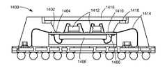
- the encapsulant cavity integrated circuit package system 100includes an encapsulant cavity 102 with an interposer 104 , such as an LGA interposer.
- a first surface 106 of the interposer 104is attached to a first integrated circuit 108 and a second surface 110 of the interposer 104 provides a surface for mounting a component such as a second integrated circuit package 112 as well as second electrical interconnects 114 .
- the encapsulant cavity 102 with the interposer 104provides an area efficient mounting region for the second integrated circuit package 112 .
- the second integrated circuit package 112may be tested prior to attachment providing increased yield and improved costs for the encapsulant cavity integrated circuit package system 100 .
- the first integrated circuit 108mounts and electrically connects to the first surface 106 of the interposer 104 . After mounting and electrical connection, the first integrated circuit 108 is encapsulated with a first encapsulant 116 to form a first integrated circuit package 118 .
- the first integrated circuit package 118is attached to a substrate 120 using a die-attach bond 122 , such as a thermally conductive adhesive or a film adhesive.
- a second encapsulant 124is formed over the substrate 120 that may have passive devices 126 and the second electrical interconnects 114 between the second surface 110 of the interposer 104 and the substrate 120 .
- the substrate 120includes contact pads 128 , vias 130 , and interconnect pads 132 . Terminal interconnects 134 , such as solder balls, are mounted to the interconnect pads 132 .
- the second encapsulant 124protects the passive devices 126 , the second interconnects 114 and the substrate 120 . Further, the second encapsulant 124 is formed with the encapsulant cavity 102 having the second surface 110 of the interposer 104 substantially exposed for attaching the second integrated circuit package 112 .
- An underfill 136may be applied under the second integrated circuit package 112 and to the encapsulant cavity 102 and the second surface 110 of the interposer 104 . The underfill 136 may provide protection and structural integrity to the interposer 104 and the second integrated circuit package 112 .
- the first integrated circuit package 118 with an inverted bottom terminalprovides an attachment surface on the interposer 104 .
- the interposer 104enables many types of the first integrated circuit package 118 , many functions of the second integrated circuit package 112 and mounting the second integrated circuit package 112 within planar dimensions of the first integrated circuit package 118 . It has been discovered that the first integrated circuit package 118 with the inverted bottom terminal allows the use of a smaller footprint for the second integrated circuit package 112 improving size and cost of the encapsulant cavity integrated circuit package system 100 .
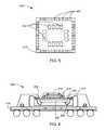
- the second surface 110 of the interposer 104includes terminal pads 202 and bond fingers 204 .
- the terminal pads 202provide electrical and mechanical mounting surfaces for the second integrated circuit package 112 .
- the bond fingers 204 of the interposer 104 and the substrate 120are electrically connected with the second electrical interconnects 114 .
- the terminal pads 202are electrically connected to the bond fingers 204 by electrical traces (not shown) completing an electrical connection between the second integrated circuit package 112 , the first integrated circuit 108 and the substrate 120 .
- the encapsulant cavity integrated circuit package system 100includes the encapsulant cavity 102 and the second surface 110 of the interposer 104 substantially exposed.
- the second surface 110 of the interposer 104includes the terminal pads 202 for mounting the second integrated circuit package 112 .
- the second integrated circuit package 112may be tested to ensure having a known good die (KGD) prior to attachment, such as surface mount, to the second surface 110 of the interposer 104 .
- the second integrated circuit package 112may be an area array package or a direct chip attach, surface mounted to the second surface 110 of the interposer 104 .
- the encapsulant cavity integrated circuit package system 400provides an encapsulant cavity 402 with an interposer 404 , such as an LGA interposer.
- an interposer 404such as an LGA interposer.
- a first surface 406 of the interposer 404is attached to a first integrated circuit 408 and a second surface 410 of the interposer 404 provides a surface for mounting a component such as a leaded package 412 as well as second electrical interconnects 414 .
- the first integrated circuit 408is mounted to a substrate 416 .
- the leaded package 412may be surface mounted to the second surface 410 of the interposer 404 .
- the second surface 410 of the interposer 404 of the encapsulant cavity integrated circuit package system 400includes terminal pads 502 and bond fingers 504 .
- the terminal pads 502provide electrical mounting surfaces, such as surface mount, for the second integrated circuit package 412 of FIG. 4 (not shown).
- the bond fingers 504 of the interposer 404 of FIG. 4 (not shown) and the substrate 416 of FIG. 4 (not shown)are electrically connected with the second electrical interconnects 414 of FIG. 4 (not shown).
- the terminal pads 502are electrically connected to the bond fingers 504 by electrical traces (not shown) completing an electrical connection between the second integrated circuit package 412 , the first integrated circuit 408 of FIG. 4 (not shown) and the substrate 416 .
- the encapsulant cavity integrated circuit package system 600provides an encapsulant cavity 602 with an interposer 604 , such as an LGA interposer.
- an interposer 604such as an LGA interposer.
- a first surface 606 of the interposer 604is attached to a first integrated circuit 608 and a second surface 610 of the interposer 604 provides a surface for mounting a component such as a leadless package 612 as well as second electrical interconnects 614 .
- the first integrated circuit 608is mounted to a substrate 616 .
- the leadless package 612may be surface mounted to the second surface 610 of the interposer 604 .
- the second surface 610 of the interposer 604includes terminal pads 702 and bond fingers 704 .
- the terminal pads 702provide electrical mounting surfaces, such as surface mount, for the second integrated circuit package 612 of FIG. 6 (not shown).
- the bond fingers 704 of the interposer 604 of FIG. 6 (not shown) and the substrate 616 of FIG. 6 (not shown)are electrically connected with the second electrical interconnects 614 of FIG. 6 (not shown).
- the terminal pads 702are electrically connected to the bond fingers 704 by electrical traces (not shown) completing an electrical connection between the second integrated circuit package 612 of FIG. 6 (not shown) and the substrate 616 .
- the encapsulant cavity integrated circuit package system 800includes an encapsulant cavity 802 with an interposer 804 , such as an LGA interposer.
- a first surface 806 of the interposer 804is attached to a first integrated circuit 808 and a second surface 810 of the interposer 804 provides a surface for mounting a component such as a second integrated circuit package 812 as well as second electrical interconnects 814 .
- the first integrated circuit 808mounts and electrically connects to the first surface 806 of the interposer 804 . After mounting and electrical connection, the first integrated circuit 808 is encapsulated with a first encapsulant 816 to form a first integrated circuit package 818 .
- a substrate 820includes a third integrated circuit package 822 .
- the first integrated circuit package 818is attached on the third integrated circuit package 822 using a die-attach bond 824 , such as a thermally conductive adhesive or a film adhesive.
- a second encapsulant 826is formed over the substrate 820 that may include passive devices 828 and the second electrical interconnects 814 between the second surface 810 of the interposer 804 and the substrate 820 .
- the substrate 820includes contact pads 830 , vias 832 , and interconnect pads 834 .
- Terminal interconnects 836such as solder balls, are mounted to the interconnect pads 834 .
- the second encapsulant 826protects the passive devices 828 , the second interconnects 814 and the substrate 820 . Further, the second encapsulant 826 is formed with the encapsulant cavity 802 having the second surface 810 of the interposer 804 substantially exposed for attaching the second integrated circuit package 812 .
- An underfill 838may be applied under the second integrated circuit package 812 and to the encapsulant cavity 802 and the second surface 810 of the interposer 804 . The underfill 838 may provide protection and structural integrity to the interposer 804 and the second integrated circuit package 812 .
- the encapsulant cavity integrated circuit package system 900includes an encapsulant cavity 902 with an interposer 904 , such as an LGA interposer.
- a first surface 906 of the interposer 904is attached to a first integrated circuit 908 and a second surface 910 of the interposer 904 provides a surface for mounting a component such as a second integrated circuit package 912 as well as second electrical interconnects 914 .
- the first integrated circuit 908mounts and electrically connects to the first surface 906 of the interposer 904 . After mounting and electrical connection, the first integrated circuit 908 is encapsulated with a first encapsulant 916 to form a first integrated circuit package 918 .
- a substrate 920includes a third integrated circuit 922 .
- the first integrated circuit package 918is attached to a spacer 924 on the third integrated circuit 922 .
- a second encapsulant 926is formed over the substrate 920 that may include passive devices 928 and the second electrical interconnects 914 between the second surface 910 of the interposer 904 and the substrate 920 .
- the substrate 920includes contact pads 930 , vias 932 , and interconnect pads 934 .
- Terminal interconnects 936such as solder balls, are mounted to the interconnect pads 934 .
- the second encapsulant 926protects the passive devices 928 , the second interconnects 914 and the substrate 920 . Further, the second encapsulant 926 is formed with the encapsulant cavity 902 having the second surface 910 of the interposer 904 substantially exposed for attaching the second integrated circuit package 912 .
- An underfill 938may be applied under the second integrated circuit package 912 and to the encapsulant cavity 902 and the second surface 910 of the interposer 904 . The underfill 938 may provide protection and structural integrity to the interposer 904 and the second integrated circuit package 912 .
- the encapsulant cavity integrated circuit package system 1000provides an encapsulant cavity 1002 with an interposer 1004 , such as an LGA interposer.
- an interposer 1004such as an LGA interposer.
- a first surface 1006 of the interposer 1004is attached to a first integrated circuit 1008 and a second surface 1010 of the interposer 1004 provides a surface for mounting components such as passive devices 1012 as well as second electrical interconnects 1014 .
- the passive devices 1012may be surface mounted to the second surface 1010 of the interposer 104 .
- the encapsulant cavity integrated circuit package system 1100provides an encapsulant cavity 1102 with an interposer 1104 , such as an LGA interposer.
- an interposer 1104such as an LGA interposer.
- a first surface 1106 of the interposer 1104is attached to a first integrated circuit 1108 and a second surface 1110 of the interposer 1104 provides a surface for mounting components such as system device packages 1112 as well as second electrical interconnects 1114 .
- the system device packages 1112may include surface-mount package technology, such as area array packages, leaded packages, or direct chip attach. Further, the system device packages 1112 may include passive device integration and surface mount to the second surface 1110 of the interposer 1104 .
- FIG. 12therein is shown a cross-sectional view of an encapsulant cavity integrated circuit package system 1200 in yet another alternative embodiment of the present invention.
- the encapsulant cavity integrated circuit package system 1200provides an encapsulant cavity 1202 with an interposer 1204 , such as an LGA interposer.
- an interposer 1204such as an LGA interposer.
- a first surface 1206 of the interposer 1204is attached to a first integrated circuit 1208 and a second surface 1210 of the interposer 1204 provides a surface for mounting components such as system devices 1212 as well as second electrical interconnects 1214 .
- the system devices 1212may include chip-scale package technology, such as chip on board, flip chip, or direct chip attach. Further, the system devices 1212 may include passive devices and surface mount to the second surface 1210 of the interposer 1204 . Third electrical interconnects 1216 may connect the system devices 1212 to the second surface 1210 of the interposer 1204 . A third encapsulant 1218 may be applied over the system devices 1212 .
- FIG. 13therein is shown a cross-sectional view of an encapsulant cavity integrated circuit package system 1300 in yet another alternative embodiment of the present invention.
- the encapsulant cavity integrated circuit package system 1300provides an encapsulant cavity 1302 with an interposer 1304 , such as an LGA interposer.
- an interposer 1304such as an LGA interposer.
- a first surface 1306 of the interposer 1304is attached to a first integrated circuit 1308 and a second surface 1310 of the interposer 1304 provides a surface for mounting components such as an optical sensor device 1312 as well as second electrical interconnects 1314 .
- the optical sensor device 1312may surface mount to the second surface 1310 of the interposer 1304 .
- the optical sensor device 1312is electrically connected to the second surface 1310 of the interposer 1304 and encapsulated with an optical lid 1316 , such as a transparent window, and a sealing dam 1318 .
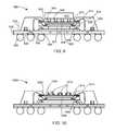
- FIG. 14therein is shown a cross-sectional view of an encapsulant cavity integrated circuit package system 1400 in yet another alternative embodiment of the present invention.
- the encapsulant cavity integrated circuit package system 1400provides an encapsulant cavity 1402 with an interposer 1404 , such as an LGA interposer.
- an interposer 1404such as an LGA interposer.
- a first surface 1406 of the interposer 1404is attached to a first integrated circuit 1408 and a second surface 1410 of the interposer 1404 provides a surface for mounting components such as an optical sensor device 1412 as well as second electrical interconnects 1414 .
- the optical sensor device 1412may surface mount to the second surface 1410 of the interposer 1404 .
- the optical sensor device 1412is electrically connected to the second surface 1410 of the interposer 1404 and encapsulated with an optical lid 1416 , such as a transparent window, using an adhesive, such as a lid sealant.
- the encapsulant cavity 1402is formed having a recess for the optical lid 1416 eliminating the need for the sealing dam 1318 of FIG. 13 (not shown).
- a lid sealant 1418such as an adhesive, is applied between the optical lid 1416 and the encapsulant cavity 1402 .
- FIG. 15is a flow chart of a system 1500 for the encapsulant cavity integrated circuit package system 100 .
- the system 1500includes forming a first integrated circuit package having an encapsulant cavity with an interposer in a block 1502 ; and attaching a component on the interposer in the encapsulant cavity in a block 1504 .
- a method to fabricate the encapsulant cavity integrated circuit package system 100is performed as follows:
- the present inventionallows the top package to be of a smaller size.
- the interposerprovides interconnection of a top package without the need for large dimensions to provide for overlapping the bottom integrated circuit. Enabling a smaller top package provides improved signal integrity as well as significant area and space savings.
- the interposerprovides a flexible interface for compatibility to several different or multiple package connections.
- the disclosed structureprovides for the integration of integrated circuits of many types, such as passive devices, integrated circuits, integrated circuits with integrated passives, or optical sensors.
- integrated circuitsof many types, such as passive devices, integrated circuits, integrated circuits with integrated passives, or optical sensors.
- the encapsulant cavity combined with the interposerprovides a compatible packaging system for several different component types.
- the disclosed structureprovides for a package on package (PoP).
- PoPpackage on package
- the encapsulant cavity and interposerare compatible with both components and other packages.
- Other packagesmay be mounted on the first integrated circuit package with the encapsulant cavity and the interposer.
- SiPsystem in package
- the encapsulant cavity integrated circuit package system method and apparatus of the present inventionfurnish important and heretofore unknown and unavailable solutions, capabilities, and functional aspects.
- the resulting processes and configurationsare straightforward, cost-effective, uncomplicated, highly versatile and effective, can be implemented by adapting known technologies, and are thus readily suited for efficient and economical manufacturing.
Landscapes
- Engineering & Computer Science (AREA)
- Microelectronics & Electronic Packaging (AREA)
- Power Engineering (AREA)
- Physics & Mathematics (AREA)
- Condensed Matter Physics & Semiconductors (AREA)
- General Physics & Mathematics (AREA)
- Computer Hardware Design (AREA)
- Structures Or Materials For Encapsulating Or Coating Semiconductor Devices Or Solid State Devices (AREA)
Abstract
Description
- This application is a continuation of co-pending U.S. patent application Ser. No. 12/057,299 filed Mar. 27, 2008, which is a continuation of U.S. patent application Ser. No. 11/306,628, filed Jan. 4, 2006, now U.S. Pat. No. 7,364,945 B2, which claims the benefit of U.S. Provisional Patent Application Ser. No. 60/667,277 filed Mar. 31, 2005, and the subject matter thereof is hereby incorporated herein by reference thereto.
- The present invention relates generally to integrated circuit package systems, and more particularly to a system for an encapsulant cavity integrated circuit package system.
- Integrated circuits are used in many portable electronic products, such as cell phones, portable computers, voice recorders, etc. as well as in many larger electronic systems, such as cars, planes, industrial control systems, etc. Across virtually all applications, there continues to be demand for reducing the size and increasing performance of the devices. The intense demand is no more visible than in portable electronics that have become so ubiquitous.
- Wafer manufacturing strives to reduce transistor or capacitor feature size in order to increase circuit density and enhance functionality. Device geometries with sub-micron line widths are so common that individual chips routinely contain millions of electronic devices. Reduced feature size has been quite successful in improving electronic systems, and continuous development is expected in the future. However, significant obstacles to further reduction in feature size are being encountered. These obstacles include defect density control, optical system resolution limits, and availability of processing material and equipment. Attention has therefore increasingly shifted to semiconductor packaging as a means to fulfill the relentless demands for enhanced system performance.
- Drawbacks of conventional designs include a relatively large footprint of the package on the mounting surface of motherboard. The footprint reflects what is typically the maximum dimension of the package, namely, the x-y dimension of the package. In applications where mounting space is at a premium, such as pagers, portable telephones, and personal computers, among others, a large footprint is undesirable. With the goal of increasing the amount of circuitry in a package, but without increasing the area of the package so that the package does not take up any more space on the circuit board, manufacturers have been stacking two or more die within a single package. Unfortunately, sufficient overlap for electrical interconnect and large footprint top packages have plagued previous stacked package or package on package designs.
- Thus a need still remains for an integrated circuit package system to provide reduced area and volume. In view of the increasing demand for density of integrated circuits and particularly portable electronic products, it is increasingly critical that answers be found to these problems.
- Solutions to these problems have been long sought but prior developments have not taught or suggested any solutions and, thus, solutions to these problems have long eluded those skilled in the art.
- The present invention provides a method for fabricating an encapsulant cavity integrated circuit package system including: forming a first integrated circuit package with an inverted bottom terminal having an encapsulant cavity and an interposer, and attaching a component on the interposer in the encapsulant cavity.
- The present invention provides an encapsulant cavity integrated circuit package system, including: a first integrated circuit package with an inverted bottom terminal having an encapsulant cavity and an interposer; and a component on the interposer in the encapsulant cavity.
- Certain embodiments of the invention have other aspects in addition to or in place of those mentioned or obvious from the above. The aspects will become apparent to those skilled in the art from a reading of the following detailed description when taken with reference to the accompanying drawings.
FIG. 1 is a cross-sectional view of an encapsulant cavity integrated circuit package system in an embodiment of the present invention;FIG. 2 is a plan view of the second surface of the interposer of the encapsulant cavity integrated circuit package system;FIG. 3 is a cross-sectional view of the encapsulant cavity integrated circuit package system in a second package-mounting phase;FIG. 4 is a cross-sectional view of an encapsulant cavity integrated circuit package system in an alternative embodiment of the present invention;FIG. 5 is a plan view of the second surface of the interposer of the encapsulant cavity integrated circuit package system;FIG. 6 is a cross-sectional view of an encapsulant cavity integrated circuit package system in another alternative embodiment of the present invention;FIG. 7 is a plan view of the second surface of the interposer of the encapsulant cavity integrated circuit package system;FIG. 8 is a cross-sectional view of an encapsulant cavity integrated circuit package system in yet another alternative embodiment of the present invention;FIG. 9 is a cross-sectional view of an encapsulant cavity integrated circuit package system in yet another alternative embodiment of the present invention;FIG. 10 is a cross-sectional view of an encapsulant cavity integrated circuit package system in yet another alternative embodiment of the present invention;FIG. 11 is a cross-sectional view of an encapsulant cavity integrated circuit package system in yet another alternative embodiment of the present invention;FIG. 12 is a cross-sectional view of an encapsulant cavity integrated circuit package system in yet another alternative embodiment of the present invention;FIG. 13 is a cross-sectional view of an encapsulant cavity integrated circuit package system in yet another alternative embodiment of the present invention;FIG. 14 is a cross-sectional view of an encapsulant cavity integrated circuit package system in yet another alternative embodiment of the present invention; andFIG. 15 is a flow chart of a system for an encapsulant cavity integrated circuit package system.- In the following description, numerous specific details are given to provide a thorough understanding of the invention. However, it will be apparent that the invention may be practiced without these specific details. In order to avoid obscuring the present invention, some well-known circuits, and process steps are not disclosed in detail.
- Likewise, the drawings showing embodiments of the apparatus/device are semi-diagrammatic and not to scale and, particularly, some of the dimensions are for the clarity of presentation and are shown greatly exaggerated in the drawing FIGs. Similarly, although the sectional views in the drawings for ease of description show the invention with surfaces as oriented downward, this arrangement in the FIGs. is arbitrary and is not intended to suggest that invention should necessarily be in a downward direction. Generally, the device can be operated in any orientation. The same numbers are used in all the drawing FIGs. to relate to the same elements.
- The term “horizontal” as used herein is defined as a plane parallel to the conventional plane or surface of the invention, regardless of its orientation. The term “vertical” refers to a direction perpendicular to the horizontal as just defined. Terms, such as “on”, “above”, “below”, “bottom”, “top”, “side” (as in “sidewall”), “higher”, “lower”, “upper”, “over”, and “under”, are defined with respect to the horizontal plane.
- The term “processing” as used herein includes deposition of material or photoresist, patterning, exposure, development, etching, cleaning, and/or removal of the material or photoresist as required in forming a described structure.
- Referring now to
FIG. 1 , therein is shown a cross-sectional view of an encapsulant cavity integratedcircuit package system 100 in an embodiment of the present invention. The encapsulant cavity integratedcircuit package system 100 includes anencapsulant cavity 102 with aninterposer 104, such as an LGA interposer. Afirst surface 106 of theinterposer 104 is attached to a first integratedcircuit 108 and asecond surface 110 of theinterposer 104 provides a surface for mounting a component such as a second integratedcircuit package 112 as well as secondelectrical interconnects 114. Theencapsulant cavity 102 with theinterposer 104 provides an area efficient mounting region for the second integratedcircuit package 112. The secondintegrated circuit package 112 may be tested prior to attachment providing increased yield and improved costs for the encapsulant cavity integratedcircuit package system 100. - The first
integrated circuit 108 mounts and electrically connects to thefirst surface 106 of theinterposer 104. After mounting and electrical connection, the firstintegrated circuit 108 is encapsulated with afirst encapsulant 116 to form a firstintegrated circuit package 118. The firstintegrated circuit package 118 is attached to asubstrate 120 using a die-attachbond 122, such as a thermally conductive adhesive or a film adhesive. Asecond encapsulant 124 is formed over thesubstrate 120 that may havepassive devices 126 and the secondelectrical interconnects 114 between thesecond surface 110 of theinterposer 104 and thesubstrate 120. Thesubstrate 120 includescontact pads 128, vias130, andinterconnect pads 132.Terminal interconnects 134, such as solder balls, are mounted to theinterconnect pads 132. - The
second encapsulant 124 protects thepassive devices 126, thesecond interconnects 114 and thesubstrate 120. Further, thesecond encapsulant 124 is formed with theencapsulant cavity 102 having thesecond surface 110 of theinterposer 104 substantially exposed for attaching the secondintegrated circuit package 112. Anunderfill 136 may be applied under the secondintegrated circuit package 112 and to theencapsulant cavity 102 and thesecond surface 110 of theinterposer 104. Theunderfill 136 may provide protection and structural integrity to theinterposer 104 and the secondintegrated circuit package 112. - The first
integrated circuit package 118 with an inverted bottom terminal, such as an LGA, Bottom Lead Package or QFN, provides an attachment surface on theinterposer 104. Theinterposer 104 enables many types of the firstintegrated circuit package 118, many functions of the secondintegrated circuit package 112 and mounting the secondintegrated circuit package 112 within planar dimensions of the firstintegrated circuit package 118. It has been discovered that the firstintegrated circuit package 118 with the inverted bottom terminal allows the use of a smaller footprint for the secondintegrated circuit package 112 improving size and cost of the encapsulant cavity integratedcircuit package system 100. - Referring now to
FIG. 2 , therein is shown a plan view of thesecond surface 110 of theinterposer 104 of the encapsulant cavity integratedcircuit package system 100. Thesecond surface 110 of theinterposer 104 includesterminal pads 202 andbond fingers 204. Theterminal pads 202 provide electrical and mechanical mounting surfaces for the secondintegrated circuit package 112. Thebond fingers 204 of theinterposer 104 and thesubstrate 120 are electrically connected with the secondelectrical interconnects 114. Theterminal pads 202 are electrically connected to thebond fingers 204 by electrical traces (not shown) completing an electrical connection between the secondintegrated circuit package 112, the firstintegrated circuit 108 and thesubstrate 120. - Referring now to
FIG. 3 , therein is shown a cross-sectional view of the encapsulant cavity integratedcircuit package system 100 in a second package-mounting phase. The encapsulant cavity integratedcircuit package system 100 includes theencapsulant cavity 102 and thesecond surface 110 of theinterposer 104 substantially exposed. Thesecond surface 110 of theinterposer 104 includes theterminal pads 202 for mounting the secondintegrated circuit package 112. The secondintegrated circuit package 112 may be tested to ensure having a known good die (KGD) prior to attachment, such as surface mount, to thesecond surface 110 of theinterposer 104. The secondintegrated circuit package 112 may be an area array package or a direct chip attach, surface mounted to thesecond surface 110 of theinterposer 104. - Referring now to
FIG. 4 , therein is shown a cross-sectional view of an encapsulant cavity integratedcircuit package system 400 in an alternative embodiment of the present invention. In a manner similar to the encapsulant cavity integratedcircuit package system 100 ofFIG. 1 , the encapsulant cavity integratedcircuit package system 400 provides anencapsulant cavity 402 with aninterposer 404, such as an LGA interposer. Similarly, afirst surface 406 of theinterposer 404 is attached to a firstintegrated circuit 408 and asecond surface 410 of theinterposer 404 provides a surface for mounting a component such as aleaded package 412 as well as secondelectrical interconnects 414. The firstintegrated circuit 408 is mounted to asubstrate 416. Theleaded package 412 may be surface mounted to thesecond surface 410 of theinterposer 404. - Referring now to
FIG. 5 , therein is shown a plan view of thesecond surface 410 of theinterposer 404 of the encapsulant cavity integratedcircuit package system 400. Thesecond surface 410 of theinterposer 404 includesterminal pads 502 andbond fingers 504. Theterminal pads 502 provide electrical mounting surfaces, such as surface mount, for the secondintegrated circuit package 412 ofFIG. 4 (not shown). Thebond fingers 504 of theinterposer 404 ofFIG. 4 (not shown) and thesubstrate 416 ofFIG. 4 (not shown) are electrically connected with the secondelectrical interconnects 414 ofFIG. 4 (not shown). Theterminal pads 502 are electrically connected to thebond fingers 504 by electrical traces (not shown) completing an electrical connection between the secondintegrated circuit package 412, the firstintegrated circuit 408 ofFIG. 4 (not shown) and thesubstrate 416. - Referring now to
FIG. 6 , therein is shown a cross-sectional view of an encapsulant cavity integratedcircuit package system 600 in another alternative embodiment of the present invention. In a manner similar to the encapsulant cavity integratedcircuit package system 100 ofFIG. 1 , the encapsulant cavity integratedcircuit package system 600 provides anencapsulant cavity 602 with aninterposer 604, such as an LGA interposer. Similarly, afirst surface 606 of theinterposer 604 is attached to a firstintegrated circuit 608 and asecond surface 610 of theinterposer 604 provides a surface for mounting a component such as aleadless package 612 as well as secondelectrical interconnects 614. The firstintegrated circuit 608 is mounted to asubstrate 616. Theleadless package 612 may be surface mounted to thesecond surface 610 of theinterposer 604. - Referring now to
FIG. 7 , therein is shown a plan view of thesecond surface 610 of theinterposer 604 of the encapsulant cavity integratedcircuit package system 600. Thesecond surface 610 of theinterposer 604 includesterminal pads 702 andbond fingers 704. Theterminal pads 702 provide electrical mounting surfaces, such as surface mount, for the secondintegrated circuit package 612 ofFIG. 6 (not shown). Thebond fingers 704 of theinterposer 604 ofFIG. 6 (not shown) and thesubstrate 616 ofFIG. 6 (not shown) are electrically connected with the secondelectrical interconnects 614 ofFIG. 6 (not shown). Theterminal pads 702 are electrically connected to thebond fingers 704 by electrical traces (not shown) completing an electrical connection between the secondintegrated circuit package 612 ofFIG. 6 (not shown) and thesubstrate 616. - Referring now to
FIG. 8 , therein is shown a cross-sectional view of an encapsulant cavity integratedcircuit package system 800 in yet another alternative embodiment of the present invention. The encapsulant cavity integratedcircuit package system 800 includes anencapsulant cavity 802 with aninterposer 804, such as an LGA interposer. Afirst surface 806 of theinterposer 804 is attached to a firstintegrated circuit 808 and asecond surface 810 of theinterposer 804 provides a surface for mounting a component such as a secondintegrated circuit package 812 as well as secondelectrical interconnects 814. - The first
integrated circuit 808 mounts and electrically connects to thefirst surface 806 of theinterposer 804. After mounting and electrical connection, the firstintegrated circuit 808 is encapsulated with afirst encapsulant 816 to form a firstintegrated circuit package 818. Asubstrate 820 includes a thirdintegrated circuit package 822. The firstintegrated circuit package 818 is attached on the thirdintegrated circuit package 822 using a die-attachbond 824, such as a thermally conductive adhesive or a film adhesive. - A
second encapsulant 826 is formed over thesubstrate 820 that may includepassive devices 828 and the secondelectrical interconnects 814 between thesecond surface 810 of theinterposer 804 and thesubstrate 820. Thesubstrate 820 includescontact pads 830, vias832, andinterconnect pads 834.Terminal interconnects 836, such as solder balls, are mounted to theinterconnect pads 834. - The
second encapsulant 826 protects thepassive devices 828, thesecond interconnects 814 and thesubstrate 820. Further, thesecond encapsulant 826 is formed with theencapsulant cavity 802 having thesecond surface 810 of theinterposer 804 substantially exposed for attaching the secondintegrated circuit package 812. Anunderfill 838 may be applied under the secondintegrated circuit package 812 and to theencapsulant cavity 802 and thesecond surface 810 of theinterposer 804. Theunderfill 838 may provide protection and structural integrity to theinterposer 804 and the secondintegrated circuit package 812. - Referring now to
FIG. 9 , therein is shown a cross-sectional view of an encapsulant cavity integratedcircuit package system 900 in yet another alternative embodiment of the present invention. The encapsulant cavity integratedcircuit package system 900 includes anencapsulant cavity 902 with aninterposer 904, such as an LGA interposer. Afirst surface 906 of theinterposer 904 is attached to a firstintegrated circuit 908 and asecond surface 910 of theinterposer 904 provides a surface for mounting a component such as a secondintegrated circuit package 912 as well as secondelectrical interconnects 914. - The first
integrated circuit 908 mounts and electrically connects to thefirst surface 906 of theinterposer 904. After mounting and electrical connection, the firstintegrated circuit 908 is encapsulated with afirst encapsulant 916 to form a firstintegrated circuit package 918. Asubstrate 920 includes a thirdintegrated circuit 922. The firstintegrated circuit package 918 is attached to aspacer 924 on the thirdintegrated circuit 922. - A
second encapsulant 926 is formed over thesubstrate 920 that may includepassive devices 928 and the secondelectrical interconnects 914 between thesecond surface 910 of theinterposer 904 and thesubstrate 920. Thesubstrate 920 includescontact pads 930, vias932, andinterconnect pads 934.Terminal interconnects 936, such as solder balls, are mounted to theinterconnect pads 934. - The
second encapsulant 926 protects thepassive devices 928, thesecond interconnects 914 and thesubstrate 920. Further, thesecond encapsulant 926 is formed with theencapsulant cavity 902 having thesecond surface 910 of theinterposer 904 substantially exposed for attaching the secondintegrated circuit package 912. Anunderfill 938 may be applied under the secondintegrated circuit package 912 and to theencapsulant cavity 902 and thesecond surface 910 of theinterposer 904. Theunderfill 938 may provide protection and structural integrity to theinterposer 904 and the secondintegrated circuit package 912. - Referring now to
FIG. 10 , therein is shown a cross-sectional view of an encapsulant cavity integratedcircuit package system 1000 in yet another alternative embodiment of the present invention. In a manner similar to the encapsulant cavity integratedcircuit package system 900 ofFIG. 9 , the encapsulant cavity integratedcircuit package system 1000 provides anencapsulant cavity 1002 with aninterposer 1004, such as an LGA interposer. Similarly, afirst surface 1006 of theinterposer 1004 is attached to a firstintegrated circuit 1008 and asecond surface 1010 of theinterposer 1004 provides a surface for mounting components such aspassive devices 1012 as well as secondelectrical interconnects 1014. Thepassive devices 1012 may be surface mounted to thesecond surface 1010 of theinterposer 104. - Referring now to
FIG. 11 , therein is shown a cross-sectional view of an encapsulant cavity integrated circuit package system1100 in yet another alternative embodiment of the present invention. In a manner similar to the encapsulant cavity integratedcircuit package system 100 ofFIG. 1 , the encapsulant cavity integrated circuit package system1100 provides anencapsulant cavity 1102 with aninterposer 1104, such as an LGA interposer. Similarly, afirst surface 1106 of theinterposer 1104 is attached to a firstintegrated circuit 1108 and asecond surface 1110 of theinterposer 1104 provides a surface for mounting components such assystem device packages 1112 as well as secondelectrical interconnects 1114. Thesystem device packages 1112 may include surface-mount package technology, such as area array packages, leaded packages, or direct chip attach. Further, thesystem device packages 1112 may include passive device integration and surface mount to thesecond surface 1110 of theinterposer 1104. - Referring now to
FIG. 12 , therein is shown a cross-sectional view of an encapsulant cavity integratedcircuit package system 1200 in yet another alternative embodiment of the present invention. In a manner similar to the encapsulant cavity integratedcircuit package system 100 ofFIG. 1 , the encapsulant cavity integratedcircuit package system 1200 provides anencapsulant cavity 1202 with aninterposer 1204, such as an LGA interposer. Similarly, afirst surface 1206 of theinterposer 1204 is attached to a firstintegrated circuit 1208 and asecond surface 1210 of theinterposer 1204 provides a surface for mounting components such assystem devices 1212 as well as secondelectrical interconnects 1214. Thesystem devices 1212 may include chip-scale package technology, such as chip on board, flip chip, or direct chip attach. Further, thesystem devices 1212 may include passive devices and surface mount to thesecond surface 1210 of theinterposer 1204. Thirdelectrical interconnects 1216 may connect thesystem devices 1212 to thesecond surface 1210 of theinterposer 1204. Athird encapsulant 1218 may be applied over thesystem devices 1212. - Referring now to
FIG. 13 , therein is shown a cross-sectional view of an encapsulant cavity integratedcircuit package system 1300 in yet another alternative embodiment of the present invention. In a manner similar to the encapsulant cavity integratedcircuit package system 100 ofFIG. 1 , the encapsulant cavity integratedcircuit package system 1300 provides anencapsulant cavity 1302 with aninterposer 1304, such as an LGA interposer. Similarly, afirst surface 1306 of theinterposer 1304 is attached to a firstintegrated circuit 1308 and asecond surface 1310 of theinterposer 1304 provides a surface for mounting components such as anoptical sensor device 1312 as well as secondelectrical interconnects 1314. - The
optical sensor device 1312 may surface mount to thesecond surface 1310 of theinterposer 1304. Theoptical sensor device 1312 is electrically connected to thesecond surface 1310 of theinterposer 1304 and encapsulated with anoptical lid 1316, such as a transparent window, and a sealingdam 1318. - Referring now to
FIG. 14 , therein is shown a cross-sectional view of an encapsulant cavity integratedcircuit package system 1400 in yet another alternative embodiment of the present invention. In a manner similar to the encapsulant cavity integratedcircuit package system 100 ofFIG. 1 , the encapsulant cavity integratedcircuit package system 1400 provides anencapsulant cavity 1402 with aninterposer 1404, such as an LGA interposer. Similarly, afirst surface 1406 of theinterposer 1404 is attached to a firstintegrated circuit 1408 and asecond surface 1410 of theinterposer 1404 provides a surface for mounting components such as anoptical sensor device 1412 as well as secondelectrical interconnects 1414. - The
optical sensor device 1412 may surface mount to thesecond surface 1410 of theinterposer 1404. Theoptical sensor device 1412 is electrically connected to thesecond surface 1410 of theinterposer 1404 and encapsulated with anoptical lid 1416, such as a transparent window, using an adhesive, such as a lid sealant. Theencapsulant cavity 1402 is formed having a recess for theoptical lid 1416 eliminating the need for the sealingdam 1318 ofFIG. 13 (not shown). Alid sealant 1418, such as an adhesive, is applied between theoptical lid 1416 and theencapsulant cavity 1402. - Referring now to
FIG. 15 is a flow chart of asystem 1500 for the encapsulant cavity integratedcircuit package system 100. Thesystem 1500 includes forming a first integrated circuit package having an encapsulant cavity with an interposer in ablock 1502; and attaching a component on the interposer in the encapsulant cavity in ablock 1504. - In greater detail, a method to fabricate the encapsulant cavity integrated
circuit package system 100, in an embodiment of the present invention, is performed as follows: - 1. Mounting the first
integrated circuit 108 on thefirst surface 106 of theinterposer 104. (FIG. 1 ) - 2. Molding the
first encapsulant 116 over the firstintegrated circuit 108 forming the firstintegrated circuit package 118. (FIG. 1 ) - 3. Mounting the first
integrated circuit package 118 over thesubstrate 120. (FIG. 1 ) - 4. Molding the
second encapsulant 124 over the firstintegrated circuit package 118 and thesubstrate 120 forming theencapsulant cavity 102 having thesecond surface 110 of theinterposer 104 substantially exposed. (FIG. 1 ) - 5. Mounting a component on the
second surface 110 of theinterposer 104 in theencapsulant cavity 102. (FIG. 1 )
- 1. Mounting the first
- It has been discovered that the present invention thus has numerous aspects.
- An aspect is that the present invention allows the top package to be of a smaller size. The interposer provides interconnection of a top package without the need for large dimensions to provide for overlapping the bottom integrated circuit. Enabling a smaller top package provides improved signal integrity as well as significant area and space savings.
- It has been discovered that the disclosed structure allows the top known good die to be attached in many forms, such as direct chip attach, chip on board, flip chip, area array packages, leaded packages, or leadless packages. The interposer provides a flexible interface for compatibility to several different or multiple package connections.
- It has also been discovered that the disclosed structure provides for the integration of integrated circuits of many types, such as passive devices, integrated circuits, integrated circuits with integrated passives, or optical sensors. The encapsulant cavity combined with the interposer provides a compatible packaging system for several different component types.
- Yet another discovery of the disclosed structure is that the disclosed structure provides for a package on package (PoP). The encapsulant cavity and interposer are compatible with both components and other packages. Other packages may be mounted on the first integrated circuit package with the encapsulant cavity and the interposer.
- Yet another discovery of the disclosed structure provides for a system in package (SiP). By providing for several attachment types and many device or component types, components of a system can be combined within the disclosed structure. The smaller size, flexibility and compatibility provide a broad range of system applications.
- These and other valuable aspects of the present invention consequently further the state of the technology to at least the next level.
- Thus, it has been discovered that the encapsulant cavity integrated circuit package system method and apparatus of the present invention furnish important and heretofore unknown and unavailable solutions, capabilities, and functional aspects. The resulting processes and configurations are straightforward, cost-effective, uncomplicated, highly versatile and effective, can be implemented by adapting known technologies, and are thus readily suited for efficient and economical manufacturing.
- While the invention has been described in conjunction with a specific best mode, it is to be understood that many alternatives, modifications, and variations will be apparent to those skilled in the art in light of the aforegoing description. Accordingly, it is intended to embrace all such alternatives, modifications, and variations, which fall within the scope of the included claims. All matters hithertofore set forth herein or shown in the accompanying drawings are to be interpreted in an illustrative and non-limiting sense.
Claims (16)
Priority Applications (2)
| Application Number | Priority Date | Filing Date | Title |
|---|---|---|---|
| US12/892,907US8021924B2 (en) | 2005-03-31 | 2010-09-28 | Encapsulant cavity integrated circuit package system and method of fabrication thereof |
| US13/235,755US8309397B2 (en) | 2005-03-31 | 2011-09-19 | Integrated circuit packaging system with a component in an encapsulant cavity and method of fabrication thereof |
Applications Claiming Priority (4)
| Application Number | Priority Date | Filing Date | Title |
|---|---|---|---|
| US66727705P | 2005-03-31 | 2005-03-31 | |
| US11/306,628US7364945B2 (en) | 2005-03-31 | 2006-01-04 | Method of mounting an integrated circuit package in an encapsulant cavity |
| US12/057,299US7855100B2 (en) | 2005-03-31 | 2008-03-27 | Integrated circuit package system with an encapsulant cavity and method of fabrication thereof |
| US12/892,907US8021924B2 (en) | 2005-03-31 | 2010-09-28 | Encapsulant cavity integrated circuit package system and method of fabrication thereof |
Related Parent Applications (1)
| Application Number | Title | Priority Date | Filing Date |
|---|---|---|---|
| US12/057,299ContinuationUS7855100B2 (en) | 2005-03-31 | 2008-03-27 | Integrated circuit package system with an encapsulant cavity and method of fabrication thereof |
Related Child Applications (1)
| Application Number | Title | Priority Date | Filing Date |
|---|---|---|---|
| US13/235,755ContinuationUS8309397B2 (en) | 2005-03-31 | 2011-09-19 | Integrated circuit packaging system with a component in an encapsulant cavity and method of fabrication thereof |
Publications (2)
| Publication Number | Publication Date |
|---|---|
| US20110018084A1true US20110018084A1 (en) | 2011-01-27 |
| US8021924B2 US8021924B2 (en) | 2011-09-20 |
Family
ID=37069370
Family Applications (4)
| Application Number | Title | Priority Date | Filing Date |
|---|---|---|---|
| US11/306,628Active2026-05-16US7364945B2 (en) | 2005-03-31 | 2006-01-04 | Method of mounting an integrated circuit package in an encapsulant cavity |
| US12/057,299Active2026-07-08US7855100B2 (en) | 2005-03-31 | 2008-03-27 | Integrated circuit package system with an encapsulant cavity and method of fabrication thereof |
| US12/892,907ActiveUS8021924B2 (en) | 2005-03-31 | 2010-09-28 | Encapsulant cavity integrated circuit package system and method of fabrication thereof |
| US13/235,755ActiveUS8309397B2 (en) | 2005-03-31 | 2011-09-19 | Integrated circuit packaging system with a component in an encapsulant cavity and method of fabrication thereof |
Family Applications Before (2)
| Application Number | Title | Priority Date | Filing Date |
|---|---|---|---|
| US11/306,628Active2026-05-16US7364945B2 (en) | 2005-03-31 | 2006-01-04 | Method of mounting an integrated circuit package in an encapsulant cavity |
| US12/057,299Active2026-07-08US7855100B2 (en) | 2005-03-31 | 2008-03-27 | Integrated circuit package system with an encapsulant cavity and method of fabrication thereof |
Family Applications After (1)
| Application Number | Title | Priority Date | Filing Date |
|---|---|---|---|
| US13/235,755ActiveUS8309397B2 (en) | 2005-03-31 | 2011-09-19 | Integrated circuit packaging system with a component in an encapsulant cavity and method of fabrication thereof |
Country Status (1)
| Country | Link |
|---|---|
| US (4) | US7364945B2 (en) |
Cited By (7)
| Publication number | Priority date | Publication date | Assignee | Title |
|---|---|---|---|---|
| US20090152547A1 (en)* | 2007-12-17 | 2009-06-18 | Dongsam Park | Integrated circuit packaging system with leadframe interposer and method of manufacture thereof |
| US8659167B1 (en) | 2012-08-29 | 2014-02-25 | Freescale Semiconductor, Inc. | Sensor packaging method and sensor packages |
| US8709868B2 (en) | 2012-08-23 | 2014-04-29 | Freescale Semiconductor, Inc. | Sensor packages and method of packaging dies of differing sizes |
| CN104229723A (en)* | 2013-06-20 | 2014-12-24 | 罗伯特·博世有限公司 | Component in the form of a wafer level package and method for manufacturing same |
| US8962389B2 (en) | 2013-05-30 | 2015-02-24 | Freescale Semiconductor, Inc. | Microelectronic packages including patterned die attach material and methods for the fabrication thereof |
| US9040355B2 (en) | 2012-07-11 | 2015-05-26 | Freescale Semiconductor, Inc. | Sensor package and method of forming same |
| US20150355219A1 (en)* | 2014-06-10 | 2015-12-10 | Samsung Electro-Mechanics Co., Ltd. | Multi-axis sensor |
Families Citing this family (128)
| Publication number | Priority date | Publication date | Assignee | Title |
|---|---|---|---|---|
| AU2003298595A1 (en)* | 2002-10-08 | 2004-05-04 | Chippac, Inc. | Semiconductor stacked multi-package module having inverted second package |
| JP2006041438A (en)* | 2004-07-30 | 2006-02-09 | Shinko Electric Ind Co Ltd | Semiconductor chip built-in substrate, and its manufacturing method |
| US7301242B2 (en)* | 2004-11-04 | 2007-11-27 | Tabula, Inc. | Programmable system in package |
| US8201124B1 (en) | 2005-03-15 | 2012-06-12 | Tabula, Inc. | System in package and method of creating system in package |
| US7364945B2 (en)* | 2005-03-31 | 2008-04-29 | Stats Chippac Ltd. | Method of mounting an integrated circuit package in an encapsulant cavity |
| SG130055A1 (en) | 2005-08-19 | 2007-03-20 | Micron Technology Inc | Microelectronic devices, stacked microelectronic devices, and methods for manufacturing microelectronic devices |
| US8796836B2 (en) | 2005-08-25 | 2014-08-05 | Micron Technology, Inc. | Land grid array semiconductor device packages |
| SG130066A1 (en)* | 2005-08-26 | 2007-03-20 | Micron Technology Inc | Microelectronic device packages, stacked microelectronic device packages, and methods for manufacturing microelectronic devices |
| US7768125B2 (en) | 2006-01-04 | 2010-08-03 | Stats Chippac Ltd. | Multi-chip package system |
| US7723146B2 (en)* | 2006-01-04 | 2010-05-25 | Stats Chippac Ltd. | Integrated circuit package system with image sensor system |
| US8012867B2 (en)* | 2006-01-31 | 2011-09-06 | Stats Chippac Ltd | Wafer level chip scale package system |
| US8704349B2 (en) | 2006-02-14 | 2014-04-22 | Stats Chippac Ltd. | Integrated circuit package system with exposed interconnects |
| US8120156B2 (en)* | 2006-02-17 | 2012-02-21 | Stats Chippac Ltd. | Integrated circuit package system with die on base package |
| TWI296147B (en)* | 2006-04-28 | 2008-04-21 | Advanced Semiconductor Eng | Semiconductor device package |
| US20070257348A1 (en)* | 2006-05-08 | 2007-11-08 | Advanced Semiconductor Engineering, Inc. | Multiple chip package module and method of fabricating the same |
| JP4910512B2 (en)* | 2006-06-30 | 2012-04-04 | 富士通セミコンダクター株式会社 | Semiconductor device and manufacturing method of semiconductor device |
| US8766186B2 (en)* | 2006-12-27 | 2014-07-01 | Analog Devices, Inc. | Control aperture for an IR sensor |
| TW200836315A (en)* | 2007-02-16 | 2008-09-01 | Richtek Techohnology Corp | Electronic package structure and method thereof |
| US8685792B2 (en)* | 2007-03-03 | 2014-04-01 | Stats Chippac Ltd. | Integrated circuit package system with interposer |
| TWI335070B (en)* | 2007-03-23 | 2010-12-21 | Advanced Semiconductor Eng | Semiconductor package and the method of making the same |
| US8409920B2 (en)* | 2007-04-23 | 2013-04-02 | Stats Chippac Ltd. | Integrated circuit package system for package stacking and method of manufacture therefor |
| US8445325B2 (en) | 2007-05-04 | 2013-05-21 | Stats Chippac, Ltd. | Package-in-package using through-hole via die on saw streets |
| US7723159B2 (en)* | 2007-05-04 | 2010-05-25 | Stats Chippac, Ltd. | Package-on-package using through-hole via die on saw streets |
| US7829998B2 (en) | 2007-05-04 | 2010-11-09 | Stats Chippac, Ltd. | Semiconductor wafer having through-hole vias on saw streets with backside redistribution layer |
| US7777354B2 (en)* | 2007-06-05 | 2010-08-17 | Stats Chippac Ltd. | Integrated circuit package system with leaded package |
| US7884457B2 (en)* | 2007-06-26 | 2011-02-08 | Stats Chippac Ltd. | Integrated circuit package system with dual side connection |
| KR20090025908A (en)* | 2007-09-07 | 2009-03-11 | 삼성전자주식회사 | Electronic device having stacked semiconductor package and method for forming same |
| TWI358797B (en)* | 2007-09-11 | 2012-02-21 | Advanced Semiconductor Eng | A wireless communication module with power amplifi |
| US7868471B2 (en)* | 2007-09-13 | 2011-01-11 | Stats Chippac Ltd. | Integrated circuit package-in-package system with leads |
| US8120150B2 (en)* | 2007-09-18 | 2012-02-21 | Stats Chippac Ltd. | Integrated circuit package system with dual connectivity |
| US9330945B2 (en)* | 2007-09-18 | 2016-05-03 | Stats Chippac Ltd. | Integrated circuit package system with multi-chip module |
| US8124451B2 (en)* | 2007-09-21 | 2012-02-28 | Stats Chippac Ltd. | Integrated circuit packaging system with interposer |
| US7667314B2 (en)* | 2007-09-30 | 2010-02-23 | Stats Chippac Ltd. | Integrated circuit package system with mold lock subassembly |
| US20090127715A1 (en)* | 2007-11-15 | 2009-05-21 | Shin Hangil | Mountable integrated circuit package system with protrusion |
| US7985628B2 (en)* | 2007-12-12 | 2011-07-26 | Stats Chippac Ltd. | Integrated circuit package system with interconnect lock |
| US8084849B2 (en)* | 2007-12-12 | 2011-12-27 | Stats Chippac Ltd. | Integrated circuit package system with offset stacking |
| US7781261B2 (en)* | 2007-12-12 | 2010-08-24 | Stats Chippac Ltd. | Integrated circuit package system with offset stacking and anti-flash structure |
| US8536692B2 (en)* | 2007-12-12 | 2013-09-17 | Stats Chippac Ltd. | Mountable integrated circuit package system with mountable integrated circuit die |
| US7709944B2 (en)* | 2007-12-18 | 2010-05-04 | Stats Chippac Ltd. | Integrated circuit package system with package integration |
| US7800212B2 (en)* | 2007-12-27 | 2010-09-21 | Stats Chippac Ltd. | Mountable integrated circuit package system with stacking interposer |
| US8247893B2 (en)* | 2007-12-27 | 2012-08-21 | Stats Chippac Ltd. | Mountable integrated circuit package system with intra-stack encapsulation |
| US8035210B2 (en)* | 2007-12-28 | 2011-10-11 | Stats Chippac Ltd. | Integrated circuit package system with interposer |
| JP2009170476A (en)* | 2008-01-11 | 2009-07-30 | Panasonic Corp | Semiconductor device and manufacturing method of semiconductor device |
| US8115304B1 (en)* | 2008-02-06 | 2012-02-14 | Xilinx, Inc. | Method of implementing a discrete element in an integrated circuit |
| US8258015B2 (en)* | 2008-02-22 | 2012-09-04 | Stats Chippac Ltd. | Integrated circuit package system with penetrable film adhesive |
| US9236319B2 (en)* | 2008-02-29 | 2016-01-12 | Stats Chippac Ltd. | Stacked integrated circuit package system |
| US7901987B2 (en)* | 2008-03-19 | 2011-03-08 | Stats Chippac Ltd. | Package-on-package system with internal stacking module interposer |
| US7919871B2 (en)* | 2008-03-21 | 2011-04-05 | Stats Chippac Ltd. | Integrated circuit package system for stackable devices |
| US7741154B2 (en)* | 2008-03-26 | 2010-06-22 | Stats Chippac Ltd. | Integrated circuit package system with stacking module |
| US7750454B2 (en)* | 2008-03-27 | 2010-07-06 | Stats Chippac Ltd. | Stacked integrated circuit package system |
| US8072079B2 (en) | 2008-03-27 | 2011-12-06 | Stats Chippac, Ltd. | Through hole vias at saw streets including protrusions or recesses for interconnection |
| US8283209B2 (en)* | 2008-06-10 | 2012-10-09 | Stats Chippac, Ltd. | Semiconductor device and method of forming PiP with inner known good die interconnected with conductive bumps |
| US8138590B2 (en)* | 2008-06-20 | 2012-03-20 | Stats Chippac Ltd. | Integrated circuit package system with wire-in-film encapsulation |
| US7968979B2 (en)* | 2008-06-25 | 2011-06-28 | Stats Chippac Ltd. | Integrated circuit package system with conformal shielding and method of manufacture thereof |
| TWI473553B (en)* | 2008-07-03 | 2015-02-11 | Advanced Semiconductor Eng | Chip package structure |
| US7960211B2 (en)* | 2008-07-23 | 2011-06-14 | Fairchild Semiconductor Corporation | Semiconductor system-in-package and method for making the same |
| US9293385B2 (en)* | 2008-07-30 | 2016-03-22 | Stats Chippac Ltd. | RDL patterning with package on package system |
| US8304869B2 (en)* | 2008-08-01 | 2012-11-06 | Stats Chippac Ltd. | Fan-in interposer on lead frame for an integrated circuit package on package system |
| US7750455B2 (en)* | 2008-08-08 | 2010-07-06 | Stats Chippac Ltd. | Triple tier package on package system |
| US8513801B2 (en)* | 2008-08-18 | 2013-08-20 | Stats Chippac Ltd. | Integrated circuit package system |
| JP5078808B2 (en)* | 2008-09-03 | 2012-11-21 | ラピスセミコンダクタ株式会社 | Manufacturing method of semiconductor device |
| US9559046B2 (en)* | 2008-09-12 | 2017-01-31 | STATS ChipPAC Pte. Ltd. | Semiconductor device and method of forming a fan-in package-on-package structure using through silicon vias |
| US9675443B2 (en) | 2009-09-10 | 2017-06-13 | Johnson & Johnson Vision Care, Inc. | Energized ophthalmic lens including stacked integrated components |
| US8803330B2 (en)* | 2008-09-27 | 2014-08-12 | Stats Chippac Ltd. | Integrated circuit package system with mounting structure |
| US8022539B2 (en)* | 2008-11-17 | 2011-09-20 | Stats Chippac Ltd. | Integrated circuit packaging system with increased connectivity and method of manufacture thereof |
| US8012797B2 (en)* | 2009-01-07 | 2011-09-06 | Advanced Semiconductor Engineering, Inc. | Method for forming stackable semiconductor device packages including openings with conductive bumps of specified geometries |
| TWI499024B (en)* | 2009-01-07 | 2015-09-01 | Advanced Semiconductor Eng | Package-on-package device, semiconductor package and method for manufacturing the same |
| US20100171206A1 (en)* | 2009-01-07 | 2010-07-08 | Chi-Chih Chu | Package-on-Package Device, Semiconductor Package, and Method for Manufacturing The Same |
| US9466561B2 (en) | 2009-08-06 | 2016-10-11 | Rambus Inc. | Packaged semiconductor device for high performance memory and logic |
| TWI469283B (en)* | 2009-08-31 | 2015-01-11 | Advanced Semiconductor Eng | Package structure and package process |
| US8164158B2 (en)* | 2009-09-11 | 2012-04-24 | Stats Chippac, Ltd. | Semiconductor device and method of forming integrated passive device |
| US8390110B2 (en)* | 2009-10-20 | 2013-03-05 | Stats Chippac Ltd. | Integrated circuit packaging system with cavity and method of manufacture thereof |
| US8237278B2 (en)* | 2009-11-16 | 2012-08-07 | International Business Machines Corporation | Configurable interposer |
| US8198131B2 (en)* | 2009-11-18 | 2012-06-12 | Advanced Semiconductor Engineering, Inc. | Stackable semiconductor device packages |
| JP5401292B2 (en)* | 2009-12-15 | 2014-01-29 | ルネサスエレクトロニクス株式会社 | Semiconductor device and communication method |
| TWI408785B (en)* | 2009-12-31 | 2013-09-11 | Advanced Semiconductor Eng | Semiconductor package |
| US8569894B2 (en) | 2010-01-13 | 2013-10-29 | Advanced Semiconductor Engineering, Inc. | Semiconductor package with single sided substrate design and manufacturing methods thereof |
| TWI419283B (en)* | 2010-02-10 | 2013-12-11 | Advanced Semiconductor Eng | Package structure |
| TWI411075B (en) | 2010-03-22 | 2013-10-01 | Advanced Semiconductor Eng | Semiconductor package and manufacturing method thereof |
| US8350381B2 (en)* | 2010-04-01 | 2013-01-08 | Infineon Technologies Ag | Device and method for manufacturing a device |
| US8624374B2 (en) | 2010-04-02 | 2014-01-07 | Advanced Semiconductor Engineering, Inc. | Semiconductor device packages with fan-out and with connecting elements for stacking and manufacturing methods thereof |
| US8278746B2 (en) | 2010-04-02 | 2012-10-02 | Advanced Semiconductor Engineering, Inc. | Semiconductor device packages including connecting elements |
| US8558392B2 (en)* | 2010-05-14 | 2013-10-15 | Stats Chippac, Ltd. | Semiconductor device and method of forming interconnect structure and mounting semiconductor die in recessed encapsulant |
| US8541872B2 (en) | 2010-06-02 | 2013-09-24 | Stats Chippac Ltd. | Integrated circuit package system with package stacking and method of manufacture thereof |
| US9121885B2 (en)* | 2010-08-16 | 2015-09-01 | Infineon Technologies Ag | Sensor package and method of manufacturing thereof |
| US8080445B1 (en)* | 2010-09-07 | 2011-12-20 | Stats Chippac, Ltd. | Semiconductor device and method of forming WLP with semiconductor die embedded within penetrable encapsulant between TSV interposers |
| US8832283B1 (en) | 2010-09-16 | 2014-09-09 | Google Inc. | Content provided DNS resolution validation and use |
| TWI451546B (en) | 2010-10-29 | 2014-09-01 | Advanced Semiconductor Eng | Stacked semiconductor package, semiconductor package thereof and method for making a semiconductor package |
| TWI445155B (en) | 2011-01-06 | 2014-07-11 | Advanced Semiconductor Eng | Stacked semiconductor package and method for making the same |
| DE102011004381A1 (en)* | 2011-02-18 | 2012-08-23 | Robert Bosch Gmbh | Mold module with sensor element |
| US9171792B2 (en) | 2011-02-28 | 2015-10-27 | Advanced Semiconductor Engineering, Inc. | Semiconductor device packages having a side-by-side device arrangement and stacking functionality |
| JP2012186393A (en)* | 2011-03-07 | 2012-09-27 | Fujitsu Ltd | Electronic device, portable electronic terminal, and method for manufacturing electronic device |
| US8535981B2 (en) | 2011-03-10 | 2013-09-17 | Stats Chippac Ltd. | Integrated circuit package-on-package system with underfilling structures and method of manufacture thereof |
| US9233513B2 (en) | 2011-03-18 | 2016-01-12 | Johnson & Johnson Vision Care, Inc. | Apparatus for manufacturing stacked integrated component media inserts for ophthalmic devices |
| US10451897B2 (en) | 2011-03-18 | 2019-10-22 | Johnson & Johnson Vision Care, Inc. | Components with multiple energization elements for biomedical devices |
| US9110310B2 (en)* | 2011-03-18 | 2015-08-18 | Johnson & Johnson Vision Care, Inc. | Multiple energization elements in stacked integrated component devices |
| US9698129B2 (en)* | 2011-03-18 | 2017-07-04 | Johnson & Johnson Vision Care, Inc. | Stacked integrated component devices with energization |
| US8633058B2 (en)* | 2011-03-21 | 2014-01-21 | Stats Chippac Ltd. | Integrated circuit packaging system with step mold and method of manufacture thereof |
| US9804418B2 (en) | 2011-03-21 | 2017-10-31 | Johnson & Johnson Vision Care, Inc. | Methods and apparatus for functional insert with power layer |
| US9324659B2 (en)* | 2011-08-01 | 2016-04-26 | Stats Chippac, Ltd. | Semiconductor device and method of forming POP with stacked semiconductor die and bumps formed directly on the lower die |
| US8857983B2 (en) | 2012-01-26 | 2014-10-14 | Johnson & Johnson Vision Care, Inc. | Ophthalmic lens assembly having an integrated antenna structure |
| US8686550B2 (en)* | 2012-02-13 | 2014-04-01 | Freescale Semiconductor, Inc. | Method and apparatus for high pressure sensor device |
| US9406579B2 (en)* | 2012-05-14 | 2016-08-02 | STATS ChipPAC Pte. Ltd. | Semiconductor device and method of controlling warpage in semiconductor package |
| US9385006B2 (en)* | 2012-06-21 | 2016-07-05 | STATS ChipPAC Pte. Ltd. | Semiconductor device and method of forming an embedded SOP fan-out package |
| US9040352B2 (en)* | 2012-06-28 | 2015-05-26 | Freescale Semiconductor, Inc. | Film-assist molded gel-fill cavity package with overflow reservoir |
| US9953907B2 (en)* | 2013-01-29 | 2018-04-24 | Taiwan Semiconductor Manufacturing Company, Ltd. | PoP device |
| US20150001706A1 (en)* | 2013-06-27 | 2015-01-01 | Kabirkumar Mirpuri | Systems and methods for avoiding protrusions in injection molded solder |
| JP2016529716A (en) | 2014-07-07 | 2016-09-23 | インテル アイピー コーポレーション | Package-on-package multilayer microelectronic structure |
| US9941547B2 (en) | 2014-08-21 | 2018-04-10 | Johnson & Johnson Vision Care, Inc. | Biomedical energization elements with polymer electrolytes and cavity structures |
| US9793536B2 (en) | 2014-08-21 | 2017-10-17 | Johnson & Johnson Vision Care, Inc. | Pellet form cathode for use in a biocompatible battery |
| US10627651B2 (en) | 2014-08-21 | 2020-04-21 | Johnson & Johnson Vision Care, Inc. | Methods and apparatus to form biocompatible energization primary elements for biomedical devices with electroless sealing layers |
| US9383593B2 (en) | 2014-08-21 | 2016-07-05 | Johnson & Johnson Vision Care, Inc. | Methods to form biocompatible energization elements for biomedical devices comprising laminates and placed separators |
| US10361405B2 (en) | 2014-08-21 | 2019-07-23 | Johnson & Johnson Vision Care, Inc. | Biomedical energization elements with polymer electrolytes |
| US9599842B2 (en) | 2014-08-21 | 2017-03-21 | Johnson & Johnson Vision Care, Inc. | Device and methods for sealing and encapsulation for biocompatible energization elements |
| US9715130B2 (en) | 2014-08-21 | 2017-07-25 | Johnson & Johnson Vision Care, Inc. | Methods and apparatus to form separators for biocompatible energization elements for biomedical devices |
| US10361404B2 (en) | 2014-08-21 | 2019-07-23 | Johnson & Johnson Vision Care, Inc. | Anodes for use in biocompatible energization elements |
| US10381687B2 (en) | 2014-08-21 | 2019-08-13 | Johnson & Johnson Vision Care, Inc. | Methods of forming biocompatible rechargable energization elements for biomedical devices |
| US9881850B2 (en) | 2015-09-18 | 2018-01-30 | Taiwan Semiconductor Manufacturing Company, Ltd. | Package structures and method of forming the same |
| US10345620B2 (en) | 2016-02-18 | 2019-07-09 | Johnson & Johnson Vision Care, Inc. | Methods and apparatus to form biocompatible energization elements incorporating fuel cells for biomedical devices |
| US10204893B2 (en) | 2016-05-19 | 2019-02-12 | Invensas Bonding Technologies, Inc. | Stacked dies and methods for forming bonded structures |
| US10741955B2 (en)* | 2016-09-29 | 2020-08-11 | Veoneer Us, Inc. | Sensor assembly and method for assembling a sensor connector assembly |
| CN109867257A (en) | 2017-12-04 | 2019-06-11 | 讯芯电子科技(中山)有限公司 | Chip package and manufacturing method thereof |
| JP2019153619A (en)* | 2018-02-28 | 2019-09-12 | 東芝メモリ株式会社 | Semiconductor device |
| US11276676B2 (en) | 2018-05-15 | 2022-03-15 | Invensas Bonding Technologies, Inc. | Stacked devices and methods of fabrication |
| US11462419B2 (en) | 2018-07-06 | 2022-10-04 | Invensas Bonding Technologies, Inc. | Microelectronic assemblies |
| US11158606B2 (en) | 2018-07-06 | 2021-10-26 | Invensas Bonding Technologies, Inc. | Molded direct bonded and interconnected stack |
| US11296053B2 (en) | 2019-06-26 | 2022-04-05 | Invensas Bonding Technologies, Inc. | Direct bonded stack structures for increased reliability and improved yield in microelectronics |
| US11631647B2 (en) | 2020-06-30 | 2023-04-18 | Adeia Semiconductor Bonding Technologies Inc. | Integrated device packages with integrated device die and dummy element |
Citations (95)
| Publication number | Priority date | Publication date | Assignee | Title |
|---|---|---|---|---|
| US4524121A (en)* | 1983-11-21 | 1985-06-18 | Rohm And Haas Company | Positive photoresists containing preformed polyglutarimide polymer |
| US4697203A (en)* | 1984-06-04 | 1987-09-29 | Mitsubishi Denki Kabushiki Kaisha | Semiconductor device and manufacturing method therefor |
| US4764804A (en)* | 1986-02-21 | 1988-08-16 | Hitachi, Ltd. | Semiconductor device and process for producing the same |
| US4894707A (en)* | 1987-02-12 | 1990-01-16 | Mitsubishi Denki Kabushiki Kaisha | Semiconductor device having a light transparent window and a method of producing same |
| US5186383A (en)* | 1991-10-02 | 1993-02-16 | Motorola, Inc. | Method for forming solder bump interconnections to a solder-plated circuit trace |
| US5214308A (en)* | 1990-01-23 | 1993-05-25 | Sumitomo Electric Industries, Ltd. | Substrate for packaging a semiconductor device |
| US5214307A (en)* | 1991-07-08 | 1993-05-25 | Micron Technology, Inc. | Lead frame for semiconductor devices having improved adhesive bond line control |
| US5222014A (en)* | 1992-03-02 | 1993-06-22 | Motorola, Inc. | Three-dimensional multi-chip pad array carrier |
| US5229960A (en)* | 1990-12-05 | 1993-07-20 | Matra Marconi Space France | Solid state memory modules and memory devices including such modules |
| US5269453A (en)* | 1992-04-02 | 1993-12-14 | Motorola, Inc. | Low temperature method for forming solder bump interconnections to a plated circuit trace |
| US5340771A (en)* | 1993-03-18 | 1994-08-23 | Lsi Logic Corporation | Techniques for providing high I/O count connections to semiconductor dies |
| US5373189A (en)* | 1992-08-13 | 1994-12-13 | Commissariate A L'energie Atomique | Three-dimensional multichip module |
| US5436203A (en)* | 1994-07-05 | 1995-07-25 | Motorola, Inc. | Shielded liquid encapsulated semiconductor device and method for making the same |
| US5444296A (en)* | 1993-11-22 | 1995-08-22 | Sun Microsystems, Inc. | Ball grid array packages for high speed applications |
| US5495398A (en)* | 1992-05-22 | 1996-02-27 | National Semiconductor Corporation | Stacked multi-chip modules and method of manufacturing |
| US5550711A (en)* | 1990-08-01 | 1996-08-27 | Staktek Corporation | Ultra high density integrated circuit packages |
| US5579207A (en)* | 1994-10-20 | 1996-11-26 | Hughes Electronics | Three-dimensional integrated circuit stacking |
| US5607227A (en)* | 1993-08-27 | 1997-03-04 | Sanyo Electric Co., Ltd. | Linear light source |
| US5650667A (en)* | 1995-10-30 | 1997-07-22 | National Semiconductor Corporation | Process of forming conductive bumps on the electrodes of semiconductor chips using lapping and the bumps thereby created |
| US5652185A (en)* | 1995-04-07 | 1997-07-29 | National Semiconductor Corporation | Maximized substrate design for grid array based assemblies |
| US5734199A (en)* | 1995-12-18 | 1998-03-31 | Matsushita Electric Industrial Co., Ltd. | Semiconductor device having improved test electrodes |
| US5744863A (en)* | 1994-07-11 | 1998-04-28 | International Business Machines Corporation | Chip carrier modules with heat sinks attached by flexible-epoxy |
| US5748452A (en)* | 1996-07-23 | 1998-05-05 | International Business Machines Corporation | Multi-electronic device package |
| US5760478A (en)* | 1996-08-20 | 1998-06-02 | International Business Machines Corporation | Clock skew minimization system and method for integrated circuits |
| US5824569A (en)* | 1992-07-15 | 1998-10-20 | Micron Technology, Inc. | Semiconductor device having ball-bonded pads |
| US5828128A (en)* | 1995-08-01 | 1998-10-27 | Fujitsu, Ltd. | Semiconductor device having a bump which is inspected from outside and a circuit board used with such a semiconductor device |
| US5844315A (en)* | 1996-03-26 | 1998-12-01 | Motorola Corporation | Low-profile microelectronic package |
| US5854507A (en)* | 1998-07-21 | 1998-12-29 | Hewlett-Packard Company | Multiple chip assembly |
| US5874781A (en)* | 1995-08-16 | 1999-02-23 | Micron Technology, Inc. | Angularly offset stacked die multichip device and method of manufacture |
| US5898219A (en)* | 1997-04-02 | 1999-04-27 | Intel Corporation | Custom corner attach heat sink design for a plastic ball grid array integrated circuit package |
| US5899705A (en)* | 1997-11-20 | 1999-05-04 | Akram; Salman | Stacked leads-over chip multi-chip module |
| US5903049A (en)* | 1997-10-29 | 1999-05-11 | Mitsubishi Denki Kabushiki Kaisha | Semiconductor module comprising semiconductor packages |
| US5973337A (en)* | 1997-08-25 | 1999-10-26 | Motorola, Inc. | Ball grid device with optically transmissive coating |
| US5977640A (en)* | 1998-06-26 | 1999-11-02 | International Business Machines Corporation | Highly integrated chip-on-chip packaging |
| US5977641A (en)* | 1997-05-14 | 1999-11-02 | Kabushiki Kaisha Toshiba | Semiconductor device and method for manufacturing the same |
| US5982633A (en)* | 1997-08-20 | 1999-11-09 | Compaq Computer Corporation | Opposed ball grid array mounting |
| US5994166A (en)* | 1997-03-10 | 1999-11-30 | Micron Technology, Inc. | Method of constructing stacked packages |
| US6025648A (en)* | 1997-04-17 | 2000-02-15 | Nec Corporation | Shock resistant semiconductor device and method for producing same |
| US6034875A (en)* | 1998-06-17 | 2000-03-07 | International Business Machines Corporation | Cooling structure for electronic components |
| USRE36613E (en)* | 1993-04-06 | 2000-03-14 | Micron Technology, Inc. | Multi-chip stacked devices |
| US6075289A (en)* | 1996-10-24 | 2000-06-13 | Tessera, Inc. | Thermally enhanced packaged semiconductor assemblies |
| US6083811A (en)* | 1996-02-07 | 2000-07-04 | Northrop Grumman Corporation | Method for producing thin dice from fragile materials |
| US6083775A (en)* | 1998-02-07 | 2000-07-04 | Siliconware Precision Industries Co., Ltd. | Method of encapsulating a chip |
| US6107164A (en)* | 1998-08-18 | 2000-08-22 | Oki Electric Industry Co., Ltd. | Using grooves as alignment marks when dicing an encapsulated semiconductor wafer |
| US6118176A (en)* | 1999-04-26 | 2000-09-12 | Advanced Semiconductor Engineering, Inc. | Stacked chip assembly utilizing a lead frame |
| US6121682A (en)* | 1998-12-26 | 2000-09-19 | Hyundai Electronics Industries Co., Ltd. | Multi-chip package |
| US6130448A (en)* | 1998-08-21 | 2000-10-10 | Gentex Corporation | Optical sensor package and method of making same |
| US6133626A (en)* | 1997-10-10 | 2000-10-17 | Gennum Corporation | Three dimensional packaging configuration for multi-chip module assembly |
| US6144507A (en)* | 1996-07-23 | 2000-11-07 | Seiko Epson Corporation | Method of mounting a sealed assembly on a mounting substrate and optical transducer |
| US6143588A (en)* | 1997-09-09 | 2000-11-07 | Amkor Technology, Inc. | Method of making an integrated circuit package employing a transparent encapsulant |
| US6157080A (en)* | 1997-11-06 | 2000-12-05 | Sharp Kabushiki Kaisha | Semiconductor device using a chip scale package |
| US6165815A (en)* | 1996-02-20 | 2000-12-26 | Micron Technology, Inc. | Method of fabrication of stacked semiconductor devices |
| US6201266B1 (en)* | 1999-07-01 | 2001-03-13 | Oki Electric Industry Co., Ltd. | Semiconductor device and method for manufacturing the same |
| US6201302B1 (en)* | 1998-12-31 | 2001-03-13 | Sampo Semiconductor Corporation | Semiconductor package having multi-dies |
| US6204562B1 (en)* | 1999-02-11 | 2001-03-20 | United Microelectronics Corp. | Wafer-level chip scale package |
| US6225699B1 (en)* | 1998-06-26 | 2001-05-01 | International Business Machines Corporation | Chip-on-chip interconnections of varied characteristics |
| US6238949B1 (en)* | 1999-06-18 | 2001-05-29 | National Semiconductor Corporation | Method and apparatus for forming a plastic chip on chip package module |
| US6242932B1 (en)* | 1999-02-19 | 2001-06-05 | Micron Technology, Inc. | Interposer for semiconductor components having contact balls |
| US6246123B1 (en)* | 1998-05-04 | 2001-06-12 | Motorola, Inc. | Transparent compound and applications for its use |
| US6265766B1 (en)* | 1995-12-19 | 2001-07-24 | Micron Technology, Inc. | Flip chip adaptor package for bare die |
| US6266197B1 (en)* | 1999-12-08 | 2001-07-24 | Amkor Technology, Inc. | Molded window array for image sensor packages |
| US6274930B1 (en)* | 1999-08-17 | 2001-08-14 | Micron Technology, Inc. | Multi-chip module with stacked dice |
| US6291263B1 (en)* | 2000-06-13 | 2001-09-18 | Siliconware Precision Industries Co., Ltd. | Method of fabricating an integrated circuit package having a core-hollowed encapsulation body |
| US6291884B1 (en)* | 1999-11-09 | 2001-09-18 | Amkor Technology, Inc. | Chip-size semiconductor packages |
| US6297131B1 (en)* | 1999-04-22 | 2001-10-02 | Fujitsu Limited | Semiconductor device manufacturing method for grinding and dicing a wafer from a back side of the wafer |
| US6316735B1 (en)* | 1996-11-08 | 2001-11-13 | Ricoh Company, Ltd. | Semiconductor chip mounting board and a semiconductor device using same board |
| US6316838B1 (en)* | 1999-10-29 | 2001-11-13 | Fujitsu Limited | Semiconductor device |
| US6333552B1 (en)* | 1998-08-07 | 2001-12-25 | Sharp Kabushiki Kaisha | Millimeter wave semiconductor device |
| US6340846B1 (en)* | 2000-12-06 | 2002-01-22 | Amkor Technology, Inc. | Making semiconductor packages with stacked dies and reinforced wire bonds |
| US20020024124A1 (en)* | 1997-03-10 | 2002-02-28 | Nobuaki Hashimoto | Electronic component and semiconductor device, method for manufacturing the same, circuit board have the same mounted thereon, and electronic equipment having the circuit board |
| US6353257B1 (en)* | 2000-05-19 | 2002-03-05 | Siliconware Precision Industries Co., Ltd. | Semiconductor package configuration based on lead frame having recessed and shouldered portions for flash prevention |
| US6358773B1 (en)* | 2000-12-27 | 2002-03-19 | Vincent Lin | Method of making substrate for use in forming image sensor package |
| US6369454B1 (en)* | 1998-12-31 | 2002-04-09 | Amkor Technology, Inc. | Semiconductor package and method for fabricating the same |
| US6372551B1 (en)* | 2000-05-12 | 2002-04-16 | Siliconware Precison Industries Co., Ltd. | Method of manufacturing an image-sensor integrated circuit package without resin flash on lead frame and with increased wire bondability |
| US6376904B1 (en)* | 1999-12-23 | 2002-04-23 | Rambus Inc. | Redistributed bond pads in stacked integrated circuit die package |
| US6379988B1 (en)* | 2000-05-16 | 2002-04-30 | Sandia Corporation | Pre-release plastic packaging of MEMS and IMEMS devices |
| US6384472B1 (en)* | 2000-03-24 | 2002-05-07 | Siliconware Precision Industries Co., Ltd | Leadless image sensor package structure and method for making the same |
| US6388313B1 (en)* | 2001-01-30 | 2002-05-14 | Siliconware Precision Industries Co., Ltd. | Multi-chip module |
| US6396116B1 (en)* | 2000-02-25 | 2002-05-28 | Agilent Technologies, Inc. | Integrated circuit packaging for optical sensor devices |
| US6400007B1 (en)* | 2001-04-16 | 2002-06-04 | Kingpak Technology Inc. | Stacked structure of semiconductor means and method for manufacturing the same |
| US6407381B1 (en)* | 2000-07-05 | 2002-06-18 | Amkor Technology, Inc. | Wafer scale image sensor package |
| US6407456B1 (en)* | 1996-02-20 | 2002-06-18 | Micron Technology, Inc. | Multi-chip device utilizing a flip chip and wire bond assembly |
| US6410861B1 (en)* | 1999-12-03 | 2002-06-25 | Motorola, Inc. | Low profile interconnect structure |
| US6414381B1 (en)* | 1999-03-15 | 2002-07-02 | Fujitsu Media Devices Limited | Interposer for separating stacked semiconductor chips mounted on a multi-layer printed circuit board |
| US6413798B2 (en)* | 1998-01-18 | 2002-07-02 | Kabushiki Kaisha Toshiba | Package having very thin semiconductor chip, multichip module assembled by the package, and method for manufacturing the same |
| US6420244B2 (en)* | 2000-02-21 | 2002-07-16 | Advanced Semiconductor Engineering, Inc. | Method of making wafer level chip scale package |
| US6420204B2 (en)* | 1999-06-03 | 2002-07-16 | Amkor Technology, Inc. | Method of making a plastic package for an optical integrated circuit device |
| US6424050B1 (en)* | 1999-09-22 | 2002-07-23 | Seiko Epson Corporation | Semiconductor device |
| US20020096755A1 (en)* | 2001-01-24 | 2002-07-25 | Yasuki Fukui | Semiconductor device |
| US20020100955A1 (en)* | 1999-02-22 | 2002-08-01 | Scott G. Potter | Method and apparatus for extending fatigue life of solder joints semiconductor device |
| US6441496B1 (en)* | 2000-11-22 | 2002-08-27 | Wen Chuan Chen | Structure of stacked integrated circuits |
| US6445064B1 (en)* | 2001-02-06 | 2002-09-03 | Mitsubishi Denki Kabushiki Kaisha | Semiconductor device |
| US20020130404A1 (en)* | 2001-03-19 | 2002-09-19 | Toshihiro Ushijima | Semiconductor module in which plural semiconductor chips are enclosed in one package |
| US20050023657A1 (en)* | 2003-04-18 | 2005-02-03 | Yu-Fang Tsai | Stacked chip-packaging structure |
| US7391105B2 (en)* | 2003-08-28 | 2008-06-24 | Samsung Electronics Co., Ltd. | Unit semiconductor chip and multi chip package with center bonding pads and methods for manufacturing the same |
Family Cites Families (162)
| Publication number | Priority date | Publication date | Assignee | Title |
|---|---|---|---|---|
| GB8927164D0 (en) | 1989-12-01 | 1990-01-31 | Inmos Ltd | Semiconductor chip packages |
| JP2531928B2 (en) | 1993-11-05 | 1996-09-04 | 株式会社東芝 | Semiconductor stack |
| US5998864A (en) | 1995-05-26 | 1999-12-07 | Formfactor, Inc. | Stacking semiconductor devices, particularly memory chips |
| US6881611B1 (en)* | 1996-07-12 | 2005-04-19 | Fujitsu Limited | Method and mold for manufacturing semiconductor device, semiconductor device and method for mounting the device |
| JP3834426B2 (en)* | 1997-09-02 | 2006-10-18 | 沖電気工業株式会社 | Semiconductor device |
| US6063647A (en) | 1997-12-08 | 2000-05-16 | 3M Innovative Properties Company | Method for making circuit elements for a z-axis interconnect |
| DE19755734A1 (en) | 1997-12-15 | 1999-06-24 | Siemens Ag | Method for producing a surface-mountable optoelectronic component |
| SG75958A1 (en) | 1998-06-01 | 2000-10-24 | Hitachi Ulsi Sys Co Ltd | Semiconductor device and a method of producing semiconductor device |
| US6451624B1 (en) | 1998-06-05 | 2002-09-17 | Micron Technology, Inc. | Stackable semiconductor package having conductive layer and insulating layers and method of fabrication |
| KR100339183B1 (en)* | 1998-07-13 | 2002-05-31 | 포만 제프리 엘 | Die attachment with reduced adhesive bleed-out |
| US6753922B1 (en)* | 1998-10-13 | 2004-06-22 | Intel Corporation | Image sensor mounted by mass reflow |
| US6242050B1 (en)* | 1998-11-24 | 2001-06-05 | General Electric Company | Method for producing a roughened bond coat using a slurry |
| JP2000228468A (en) | 1999-02-05 | 2000-08-15 | Mitsubishi Electric Corp | Semiconductor chip and semiconductor device |
| US6566745B1 (en)* | 1999-03-29 | 2003-05-20 | Imec Vzw | Image sensor ball grid array package and the fabrication thereof |
| US6890798B2 (en)* | 1999-06-08 | 2005-05-10 | Intel Corporation | Stacked chip packaging |
| WO2001006558A1 (en) | 1999-07-16 | 2001-01-25 | Matsushita Electric Industrial Co., Ltd. | Package of semiconductor device and method of manufacture thereof |
| US6424033B1 (en) | 1999-08-31 | 2002-07-23 | Micron Technology, Inc. | Chip package with grease heat sink and method of making |
| JP3062192B1 (en) | 1999-09-01 | 2000-07-10 | 松下電子工業株式会社 | Lead frame and method of manufacturing resin-encapsulated semiconductor device using the same |
| KR100533673B1 (en) | 1999-09-03 | 2005-12-05 | 세이코 엡슨 가부시키가이샤 | Semiconductor device, method of manufacture thereof, circuit board, and electronic device |
| JP2001156212A (en) | 1999-09-16 | 2001-06-08 | Nec Corp | Resin sealed semiconductor device and producing method therefor |
| US6274474B1 (en)* | 1999-10-25 | 2001-08-14 | International Business Machines Corporation | Method of forming BGA interconnections having mixed solder profiles |
| JP3485507B2 (en) | 1999-10-25 | 2004-01-13 | 沖電気工業株式会社 | Semiconductor device |
| US6627864B1 (en) | 1999-11-22 | 2003-09-30 | Amkor Technology, Inc. | Thin image sensor package |
| US6483101B1 (en) | 1999-12-08 | 2002-11-19 | Amkor Technology, Inc. | Molded image sensor package having lens holder |
| JP3423930B2 (en)* | 1999-12-27 | 2003-07-07 | 富士通株式会社 | Bump forming method, electronic component, and solder paste |
| US6512219B1 (en)* | 2000-01-25 | 2003-01-28 | Amkor Technology, Inc. | Fabrication method for integrally connected image sensor packages having a window support in contact with the window and active area |
| JP2001223326A (en) | 2000-02-09 | 2001-08-17 | Hitachi Ltd | Semiconductor device |
| KR100335717B1 (en)* | 2000-02-18 | 2002-05-08 | 윤종용 | High Density Memory Card |
| US6529027B1 (en)* | 2000-03-23 | 2003-03-04 | Micron Technology, Inc. | Interposer and methods for fabricating same |
| US6571466B1 (en) | 2000-03-27 | 2003-06-03 | Amkor Technology, Inc. | Flip chip image sensor package fabrication method |
| US6462421B1 (en) | 2000-04-10 | 2002-10-08 | Advanced Semicondcutor Engineering, Inc. | Multichip module |
| JP2001308262A (en)* | 2000-04-26 | 2001-11-02 | Mitsubishi Electric Corp | Resin-sealed BGA type semiconductor device |
| US6707140B1 (en)* | 2000-05-09 | 2004-03-16 | National Semiconductor Corporation | Arrayable, scaleable, and stackable molded package configuration |
| US6916683B2 (en) | 2000-05-11 | 2005-07-12 | Micron Technology, Inc. | Methods of fabricating a molded ball grid array |
| US6717245B1 (en)* | 2000-06-02 | 2004-04-06 | Micron Technology, Inc. | Chip scale packages performed by wafer level processing |
| TW445610B (en) | 2000-06-16 | 2001-07-11 | Siliconware Precision Industries Co Ltd | Stacked-die packaging structure |
| TW452873B (en) | 2000-06-21 | 2001-09-01 | Advanced Semiconductor Eng | Manufacturing method of wafer scale semiconductor package structure |
| US6503780B1 (en)* | 2000-07-05 | 2003-01-07 | Amkor Technology, Inc. | Wafer scale image sensor package fabrication method |
| TW459361B (en)* | 2000-07-17 | 2001-10-11 | Siliconware Precision Industries Co Ltd | Three-dimensional multiple stacked-die packaging structure |
| US6472758B1 (en) | 2000-07-20 | 2002-10-29 | Amkor Technology, Inc. | Semiconductor package including stacked semiconductor dies and bond wires |
| US6534419B1 (en)* | 2000-07-26 | 2003-03-18 | Advanced Interconnect Solutions | Method and apparatus for reducing IC die mass and thickness while improving strength characteristics |
| JP2002040095A (en)* | 2000-07-26 | 2002-02-06 | Nec Corp | Semiconductor device and mounting method thereof |
| US6607937B1 (en) | 2000-08-23 | 2003-08-19 | Micron Technology, Inc. | Stacked microelectronic dies and methods for stacking microelectronic dies |
| US6593648B2 (en) | 2000-08-31 | 2003-07-15 | Seiko Epson Corporation | Semiconductor device and method of making the same, circuit board and electronic equipment |
| JP4570809B2 (en) | 2000-09-04 | 2010-10-27 | 富士通セミコンダクター株式会社 | Multilayer semiconductor device and manufacturing method thereof |
| US6492726B1 (en) | 2000-09-22 | 2002-12-10 | Chartered Semiconductor Manufacturing Ltd. | Chip scale packaging with multi-layer flip chip arrangement and ball grid array interconnection |
| JP2002118201A (en) | 2000-10-05 | 2002-04-19 | Hitachi Ltd | Semiconductor device and method for manufacturing the same |
| JP4505983B2 (en)* | 2000-12-01 | 2010-07-21 | 日本電気株式会社 | Semiconductor device |
| JP3798620B2 (en) | 2000-12-04 | 2006-07-19 | 富士通株式会社 | Manufacturing method of semiconductor device |
| US6506681B2 (en)* | 2000-12-06 | 2003-01-14 | Micron Technology, Inc. | Thin flip—chip method |
| US6777819B2 (en) | 2000-12-20 | 2004-08-17 | Siliconware Precision Industries Co., Ltd. | Semiconductor package with flash-proof device |
| US6734539B2 (en)* | 2000-12-27 | 2004-05-11 | Lucent Technologies Inc. | Stacked module package |
| JP2002208656A (en)* | 2001-01-11 | 2002-07-26 | Mitsubishi Electric Corp | Semiconductor device |
| US6900549B2 (en) | 2001-01-17 | 2005-05-31 | Micron Technology, Inc. | Semiconductor assembly without adhesive fillets |
| US6674156B1 (en)* | 2001-02-09 | 2004-01-06 | National Semiconductor Corporation | Multiple row fine pitch leadless leadframe package with use of half-etch process |
| JP2002261232A (en) | 2001-03-01 | 2002-09-13 | Hitachi Ltd | Semiconductor device |
| JP4780844B2 (en) | 2001-03-05 | 2011-09-28 | Okiセミコンダクタ株式会社 | Semiconductor device |
| TW502408B (en)* | 2001-03-09 | 2002-09-11 | Advanced Semiconductor Eng | Chip with chamfer |
| SG108245A1 (en)* | 2001-03-30 | 2005-01-28 | Micron Technology Inc | Ball grid array interposer, packages and methods |
| DE10118231A1 (en)* | 2001-04-11 | 2002-10-17 | Heidenhain Gmbh Dr Johannes | Optoelectronic component arrangement comprises an optoelectronic component arranged on a support element, a closed dam on the support element and surrounding the optoelectronic component, and a casting composition arranged inside a dam |
| US6627980B2 (en) | 2001-04-12 | 2003-09-30 | Formfactor, Inc. | Stacked semiconductor device assembly with microelectronic spring contacts |
| US6528408B2 (en) | 2001-05-21 | 2003-03-04 | Micron Technology, Inc. | Method for bumped die and wire bonded board-on-chip package |
| KR100378285B1 (en) | 2001-06-15 | 2003-03-29 | Dongbu Electronics Co Ltd | Semiconductor package and fabricating method thereof |
| JP2002373969A (en) | 2001-06-15 | 2002-12-26 | Oki Electric Ind Co Ltd | Semiconductor device and method of manufacturing semiconductor device |
| US6900528B2 (en)* | 2001-06-21 | 2005-05-31 | Micron Technology, Inc. | Stacked mass storage flash memory package |
| KR100407472B1 (en)* | 2001-06-29 | 2003-11-28 | 삼성전자주식회사 | Chip-Stacked Package Device Having Upper Chip Provided With Corner Trenchs And Method For Manufacturing the Same |
| US6734552B2 (en)* | 2001-07-11 | 2004-05-11 | Asat Limited | Enhanced thermal dissipation integrated circuit package |
| DE10135393B4 (en)* | 2001-07-25 | 2004-02-05 | Infineon Technologies Ag | Electronic component, manufacturing method, and method for establishing an electrical connection between the component and a circuit board |
| US6451626B1 (en)* | 2001-07-27 | 2002-09-17 | Charles W.C. Lin | Three-dimensional stacked semiconductor package |
| KR100445073B1 (en)* | 2001-08-21 | 2004-08-21 | 삼성전자주식회사 | Dual die package |
| US20030038353A1 (en) | 2001-08-23 | 2003-02-27 | Derderian James M. | Assemblies including stacked semiconductor devices separated by discrete conductive elements therebetween, packages including the assemblies, and methods |
| US7176506B2 (en)* | 2001-08-28 | 2007-02-13 | Tessera, Inc. | High frequency chip packages with connecting elements |
| JP2003086733A (en) | 2001-09-11 | 2003-03-20 | Matsushita Electric Ind Co Ltd | Semiconductor device, method of manufacturing the same, and electronic equipment using the same |
| US6787916B2 (en) | 2001-09-13 | 2004-09-07 | Tru-Si Technologies, Inc. | Structures having a substrate with a cavity and having an integrated circuit bonded to a contact pad located in the cavity |
| US6847105B2 (en)* | 2001-09-21 | 2005-01-25 | Micron Technology, Inc. | Bumping technology in stacked die configurations |
| US6599779B2 (en) | 2001-09-24 | 2003-07-29 | St Assembly Test Service Ltd. | PBGA substrate for anchoring heat sink |
| WO2003032370A2 (en) | 2001-10-09 | 2003-04-17 | Tessera, Inc. | Stacked packages |
| US6555917B1 (en)* | 2001-10-09 | 2003-04-29 | Amkor Technology, Inc. | Semiconductor package having stacked semiconductor chips and method of making the same |
| JP2003124420A (en)* | 2001-10-16 | 2003-04-25 | Shinko Electric Ind Co Ltd | Lead frame and manufacturing method of semiconductor device using same |
| TW523887B (en) | 2001-11-15 | 2003-03-11 | Siliconware Precision Industries Co Ltd | Semiconductor packaged device and its manufacturing method |
| US6737750B1 (en)* | 2001-12-07 | 2004-05-18 | Amkor Technology, Inc. | Structures for improving heat dissipation in stacked semiconductor packages |
| JP4173346B2 (en) | 2001-12-14 | 2008-10-29 | 株式会社ルネサステクノロジ | Semiconductor device |
| US20030113952A1 (en)* | 2001-12-19 | 2003-06-19 | Mahesh Sambasivam | Underfill materials dispensed in a flip chip package by way of a through hole |
| TW523894B (en)* | 2001-12-24 | 2003-03-11 | Siliconware Precision Industries Co Ltd | Semiconductor device and its manufacturing method |
| US6891276B1 (en)* | 2002-01-09 | 2005-05-10 | Bridge Semiconductor Corporation | Semiconductor package device |
| US6774475B2 (en) | 2002-01-24 | 2004-08-10 | International Business Machines Corporation | Vertically stacked memory chips in FBGA packages |
| US7034388B2 (en)* | 2002-01-25 | 2006-04-25 | Advanced Semiconductor Engineering, Inc. | Stack type flip-chip package |
| US6784534B1 (en) | 2002-02-06 | 2004-08-31 | Amkor Technology, Inc. | Thin integrated circuit package having an optically transparent window |
| US6891239B2 (en)* | 2002-03-06 | 2005-05-10 | The Charles Stark Draper Laboratory, Inc. | Integrated sensor and electronics package |
| US6908784B1 (en)* | 2002-03-06 | 2005-06-21 | Micron Technology, Inc. | Method for fabricating encapsulated semiconductor components |
| US6613980B1 (en) | 2002-03-11 | 2003-09-02 | Agilent Technologies, Inc. | Environmental protection for an optical assembly and method therefor |
| JP2003273317A (en) | 2002-03-19 | 2003-09-26 | Nec Electronics Corp | Semiconductor device and its manufacturing method |
| JP3688249B2 (en) | 2002-04-05 | 2005-08-24 | Necエレクトロニクス株式会社 | Manufacturing method of semiconductor device |
| JP3550391B2 (en)* | 2002-05-15 | 2004-08-04 | 沖電気工業株式会社 | Semiconductor device and manufacturing method thereof |
| US6713366B2 (en)* | 2002-06-12 | 2004-03-30 | Intel Corporation | Method of thinning a wafer utilizing a laminated reinforcing layer over the device side |
| TW550770B (en)* | 2002-06-20 | 2003-09-01 | Advanced Semiconductor Eng | Optical integrated circuit element package and process for making the same |
| US6906415B2 (en)* | 2002-06-27 | 2005-06-14 | Micron Technology, Inc. | Semiconductor device assemblies and packages including multiple semiconductor devices and methods |
| JP4601892B2 (en)* | 2002-07-04 | 2010-12-22 | ラムバス・インコーポレーテッド | Semiconductor device and bump manufacturing method of semiconductor chip |
| JP3529050B2 (en)* | 2002-07-12 | 2004-05-24 | 沖電気工業株式会社 | Method for manufacturing semiconductor device |
| KR100442880B1 (en) | 2002-07-24 | 2004-08-02 | 삼성전자주식회사 | Stacked semiconductor module and manufacturing method thereof |
| US7132311B2 (en)* | 2002-07-26 | 2006-11-07 | Intel Corporation | Encapsulation of a stack of semiconductor dice |
| US7109574B2 (en) | 2002-07-26 | 2006-09-19 | Stmicroelectronics, Inc. | Integrated circuit package with exposed die surfaces and auxiliary attachment |
| US6885107B2 (en) | 2002-08-29 | 2005-04-26 | Micron Technology, Inc. | Flip-chip image sensor packages and methods of fabrication |
| US6649445B1 (en) | 2002-09-11 | 2003-11-18 | Motorola, Inc. | Wafer coating and singulation method |
| US7053476B2 (en)* | 2002-09-17 | 2006-05-30 | Chippac, Inc. | Semiconductor multi-package module having package stacked over die-down flip chip ball grid array package and having wire bond interconnect between stacked packages |
| US6838761B2 (en)* | 2002-09-17 | 2005-01-04 | Chippac, Inc. | Semiconductor multi-package module having wire bond interconnect between stacked packages and having electrical shield |
| US6972481B2 (en) | 2002-09-17 | 2005-12-06 | Chippac, Inc. | Semiconductor multi-package module including stacked-die package and having wire bond interconnect between stacked packages |
| US20040061213A1 (en)* | 2002-09-17 | 2004-04-01 | Chippac, Inc. | Semiconductor multi-package module having package stacked over die-up flip chip ball grid array package and having wire bond interconnect between stacked packages |
| WO2004027823A2 (en) | 2002-09-17 | 2004-04-01 | Chippac, Inc. | Semiconductor multi-package module having wire bond interconnection between stacked packages |
| US7064426B2 (en)* | 2002-09-17 | 2006-06-20 | Chippac, Inc. | Semiconductor multi-package module having wire bond interconnect between stacked packages |
| KR20040026530A (en)* | 2002-09-25 | 2004-03-31 | 삼성전자주식회사 | Semiconductor package and stack package using the same |
| US7034387B2 (en)* | 2003-04-04 | 2006-04-25 | Chippac, Inc. | Semiconductor multipackage module including processor and memory package assemblies |
| AU2003298595A1 (en)* | 2002-10-08 | 2004-05-04 | Chippac, Inc. | Semiconductor stacked multi-package module having inverted second package |
| JP2004134591A (en) | 2002-10-10 | 2004-04-30 | Renesas Technology Corp | Method for manufacturing semiconductor integrated circuit device |
| TW567601B (en) | 2002-10-18 | 2003-12-21 | Siliconware Precision Industries Co Ltd | Module device of stacked semiconductor package and method for fabricating the same |
| SG114585A1 (en) | 2002-11-22 | 2005-09-28 | Micron Technology Inc | Packaged microelectronic component assemblies |
| JP3689694B2 (en) | 2002-12-27 | 2005-08-31 | 松下電器産業株式会社 | Semiconductor device and manufacturing method thereof |
| TW586199B (en) | 2002-12-30 | 2004-05-01 | Advanced Semiconductor Eng | Flip-chip package |
| KR100621991B1 (en) | 2003-01-03 | 2006-09-13 | 삼성전자주식회사 | Chip Scale Stacking Package |
| US6861288B2 (en) | 2003-01-23 | 2005-03-01 | St Assembly Test Services, Ltd. | Stacked semiconductor packages and method for the fabrication thereof |
| US7388294B2 (en)* | 2003-01-27 | 2008-06-17 | Micron Technology, Inc. | Semiconductor components having stacked dice |
| US6815254B2 (en) | 2003-03-10 | 2004-11-09 | Freescale Semiconductor, Inc. | Semiconductor package with multiple sides having package contacts |
| TW576549U (en) | 2003-04-04 | 2004-02-11 | Advanced Semiconductor Eng | Multi-chip package combining wire-bonding and flip-chip configuration |
| TWI225292B (en) | 2003-04-23 | 2004-12-11 | Advanced Semiconductor Eng | Multi-chips stacked package |
| US6818980B1 (en) | 2003-05-07 | 2004-11-16 | Asat Ltd. | Stacked semiconductor package and method of manufacturing the same |
| US6853064B2 (en) | 2003-05-12 | 2005-02-08 | Micron Technology, Inc. | Semiconductor component having stacked, encapsulated dice |
| TWI299551B (en)* | 2003-06-25 | 2008-08-01 | Via Tech Inc | Quad flat no-lead type chip carrier |
| DE102004034166B4 (en) | 2003-07-17 | 2015-08-20 | Toyoda Gosei Co., Ltd. | Light-emitting device |
| DE102004036295A1 (en) | 2003-07-29 | 2005-03-03 | GELcore, LLC (n.d.Ges.d. Staates Delaware), Valley View | Fabrication of flip-chip light emitting diode device by fabricating light emitting diode devices on epitaxial wafer, dicing the epitaxial wafer, flip chip bonding the device die to mount, and reducing thickness of growth substrate |
| KR100529672B1 (en)* | 2003-10-02 | 2005-11-17 | 동부아남반도체 주식회사 | Back grinding method of image sensor |
| US7084500B2 (en) | 2003-10-29 | 2006-08-01 | Texas Instruments Incorporated | Semiconductor circuit with multiple contact sizes |
| US6930378B1 (en) | 2003-11-10 | 2005-08-16 | Amkor Technology, Inc. | Stacked semiconductor die assembly having at least one support |
| KR100564585B1 (en)* | 2003-11-13 | 2006-03-28 | 삼성전자주식회사 | Dual Stacked BA Packages and Multiple Stacked BA Packages |
| JP2005183923A (en) | 2003-11-28 | 2005-07-07 | Matsushita Electric Ind Co Ltd | Semiconductor device and manufacturing method thereof |
| DE10360708B4 (en) | 2003-12-19 | 2008-04-10 | Infineon Technologies Ag | Semiconductor module with a semiconductor stack, rewiring plate, and method of making the same |
| US20070145548A1 (en) | 2003-12-22 | 2007-06-28 | Amkor Technology, Inc. | Stack-type semiconductor package and manufacturing method thereof |
| US20060138631A1 (en)* | 2003-12-31 | 2006-06-29 | Advanced Semiconductor Engineering, Inc. | Multi-chip package structure |
| US7122906B2 (en) | 2004-01-29 | 2006-10-17 | Micron Technology, Inc. | Die-wafer package and method of fabricating same |
| US7420218B2 (en) | 2004-03-18 | 2008-09-02 | Matsushita Electric Industrial Co., Ltd. | Nitride based LED with a p-type injection region |
| US20060043556A1 (en)* | 2004-08-25 | 2006-03-02 | Chao-Yuan Su | Stacked packaging methods and structures |
| US20060073635A1 (en)* | 2004-09-28 | 2006-04-06 | Chao-Yuan Su | Three dimensional package type stacking for thinner package application |
| US20060065958A1 (en)* | 2004-09-29 | 2006-03-30 | Pei-Haw Tsao | Three dimensional package and packaging method for integrated circuits |
| KR100573302B1 (en) | 2004-10-07 | 2006-04-24 | 삼성전자주식회사 | Package Stack Using Wire Bonding and Manufacturing Method Thereof |
| TWI249796B (en) | 2004-11-08 | 2006-02-21 | Siliconware Precision Industries Co Ltd | Semiconductor device having flip chip package |
| KR100626618B1 (en)* | 2004-12-10 | 2006-09-25 | 삼성전자주식회사 | Semiconductor chip stack package and manufacturing method |
| US7271496B2 (en) | 2005-02-04 | 2007-09-18 | Stats Chippac Ltd. | Integrated circuit package-in-package system |
| US7445962B2 (en) | 2005-02-10 | 2008-11-04 | Stats Chippac Ltd. | Stacked integrated circuits package system with dense routability and high thermal conductivity |
| JP2008535273A (en)* | 2005-03-31 | 2008-08-28 | スタッツ・チップパック・リミテッド | Semiconductor stacked package assembly having substrate surfaces exposed on top and bottom surfaces |
| US7364945B2 (en)* | 2005-03-31 | 2008-04-29 | Stats Chippac Ltd. | Method of mounting an integrated circuit package in an encapsulant cavity |
| US7354800B2 (en)* | 2005-04-29 | 2008-04-08 | Stats Chippac Ltd. | Method of fabricating a stacked integrated circuit package system |
| US7763963B2 (en) | 2005-05-04 | 2010-07-27 | Stats Chippac Ltd. | Stacked package semiconductor module having packages stacked in a cavity in the module substrate |
| US7339278B2 (en) | 2005-09-29 | 2008-03-04 | United Test And Assembly Center Ltd. | Cavity chip package |
| US20070141751A1 (en)* | 2005-12-16 | 2007-06-21 | Mistry Addi B | Stackable molded packages and methods of making the same |
| US8058101B2 (en)* | 2005-12-23 | 2011-11-15 | Tessera, Inc. | Microelectronic packages and methods therefor |
| US7456088B2 (en) | 2006-01-04 | 2008-11-25 | Stats Chippac Ltd. | Integrated circuit package system including stacked die |
| US7723146B2 (en) | 2006-01-04 | 2010-05-25 | Stats Chippac Ltd. | Integrated circuit package system with image sensor system |
| US7768125B2 (en) | 2006-01-04 | 2010-08-03 | Stats Chippac Ltd. | Multi-chip package system |
| US7501697B2 (en) | 2006-03-17 | 2009-03-10 | Stats Chippac Ltd. | Integrated circuit package system |
| US7368319B2 (en) | 2006-03-17 | 2008-05-06 | Stats Chippac Ltd. | Stacked integrated circuit package-in-package system |
| US7288835B2 (en) | 2006-03-17 | 2007-10-30 | Stats Chippac Ltd. | Integrated circuit package-in-package system |
| KR100896179B1 (en) | 2007-01-05 | 2009-05-12 | 삼성전자주식회사 | Stack Package and Manufacturing Method |
| US7723159B2 (en)* | 2007-05-04 | 2010-05-25 | Stats Chippac, Ltd. | Package-on-package using through-hole via die on saw streets |
- 2006
- 2006-01-04USUS11/306,628patent/US7364945B2/enactiveActive
- 2008
- 2008-03-27USUS12/057,299patent/US7855100B2/enactiveActive
- 2010
- 2010-09-28USUS12/892,907patent/US8021924B2/enactiveActive
- 2011
- 2011-09-19USUS13/235,755patent/US8309397B2/enactiveActive
Patent Citations (99)
| Publication number | Priority date | Publication date | Assignee | Title |
|---|---|---|---|---|
| US4524121A (en)* | 1983-11-21 | 1985-06-18 | Rohm And Haas Company | Positive photoresists containing preformed polyglutarimide polymer |
| US4697203A (en)* | 1984-06-04 | 1987-09-29 | Mitsubishi Denki Kabushiki Kaisha | Semiconductor device and manufacturing method therefor |
| US4764804A (en)* | 1986-02-21 | 1988-08-16 | Hitachi, Ltd. | Semiconductor device and process for producing the same |
| US4894707A (en)* | 1987-02-12 | 1990-01-16 | Mitsubishi Denki Kabushiki Kaisha | Semiconductor device having a light transparent window and a method of producing same |
| US5214308A (en)* | 1990-01-23 | 1993-05-25 | Sumitomo Electric Industries, Ltd. | Substrate for packaging a semiconductor device |
| US5550711A (en)* | 1990-08-01 | 1996-08-27 | Staktek Corporation | Ultra high density integrated circuit packages |
| US5229960A (en)* | 1990-12-05 | 1993-07-20 | Matra Marconi Space France | Solid state memory modules and memory devices including such modules |
| US5214307A (en)* | 1991-07-08 | 1993-05-25 | Micron Technology, Inc. | Lead frame for semiconductor devices having improved adhesive bond line control |
| US5186383A (en)* | 1991-10-02 | 1993-02-16 | Motorola, Inc. | Method for forming solder bump interconnections to a solder-plated circuit trace |
| US5222014A (en)* | 1992-03-02 | 1993-06-22 | Motorola, Inc. | Three-dimensional multi-chip pad array carrier |
| US5269453A (en)* | 1992-04-02 | 1993-12-14 | Motorola, Inc. | Low temperature method for forming solder bump interconnections to a plated circuit trace |
| US5495398A (en)* | 1992-05-22 | 1996-02-27 | National Semiconductor Corporation | Stacked multi-chip modules and method of manufacturing |
| US5824569A (en)* | 1992-07-15 | 1998-10-20 | Micron Technology, Inc. | Semiconductor device having ball-bonded pads |
| US5373189A (en)* | 1992-08-13 | 1994-12-13 | Commissariate A L'energie Atomique | Three-dimensional multichip module |
| US5340771A (en)* | 1993-03-18 | 1994-08-23 | Lsi Logic Corporation | Techniques for providing high I/O count connections to semiconductor dies |
| USRE36613E (en)* | 1993-04-06 | 2000-03-14 | Micron Technology, Inc. | Multi-chip stacked devices |
| US5607227A (en)* | 1993-08-27 | 1997-03-04 | Sanyo Electric Co., Ltd. | Linear light source |
| US5444296A (en)* | 1993-11-22 | 1995-08-22 | Sun Microsystems, Inc. | Ball grid array packages for high speed applications |
| US5436203A (en)* | 1994-07-05 | 1995-07-25 | Motorola, Inc. | Shielded liquid encapsulated semiconductor device and method for making the same |
| US5744863A (en)* | 1994-07-11 | 1998-04-28 | International Business Machines Corporation | Chip carrier modules with heat sinks attached by flexible-epoxy |
| US5579207A (en)* | 1994-10-20 | 1996-11-26 | Hughes Electronics | Three-dimensional integrated circuit stacking |
| US5652185A (en)* | 1995-04-07 | 1997-07-29 | National Semiconductor Corporation | Maximized substrate design for grid array based assemblies |
| US5828128A (en)* | 1995-08-01 | 1998-10-27 | Fujitsu, Ltd. | Semiconductor device having a bump which is inspected from outside and a circuit board used with such a semiconductor device |
| US5874781A (en)* | 1995-08-16 | 1999-02-23 | Micron Technology, Inc. | Angularly offset stacked die multichip device and method of manufacture |
| US5650667A (en)* | 1995-10-30 | 1997-07-22 | National Semiconductor Corporation | Process of forming conductive bumps on the electrodes of semiconductor chips using lapping and the bumps thereby created |
| US5734199A (en)* | 1995-12-18 | 1998-03-31 | Matsushita Electric Industrial Co., Ltd. | Semiconductor device having improved test electrodes |
| US5811351A (en)* | 1995-12-18 | 1998-09-22 | Matsushita Electric Industrial Co., Ltd. | Semiconductor device and method of manufacturing the same |
| US6265766B1 (en)* | 1995-12-19 | 2001-07-24 | Micron Technology, Inc. | Flip chip adaptor package for bare die |
| US6083811A (en)* | 1996-02-07 | 2000-07-04 | Northrop Grumman Corporation | Method for producing thin dice from fragile materials |
| US6407456B1 (en)* | 1996-02-20 | 2002-06-18 | Micron Technology, Inc. | Multi-chip device utilizing a flip chip and wire bond assembly |
| US6165815A (en)* | 1996-02-20 | 2000-12-26 | Micron Technology, Inc. | Method of fabrication of stacked semiconductor devices |
| US5844315A (en)* | 1996-03-26 | 1998-12-01 | Motorola Corporation | Low-profile microelectronic package |
| US5963430A (en)* | 1996-07-23 | 1999-10-05 | International Business Machines Corporation | Multi-electronic device package comprising at least two substrates and at least four layers of electrically conductive circuitry |
| US5748452A (en)* | 1996-07-23 | 1998-05-05 | International Business Machines Corporation | Multi-electronic device package |
| US6101100A (en)* | 1996-07-23 | 2000-08-08 | International Business Machines Corporation | Multi-electronic device package |
| US6144507A (en)* | 1996-07-23 | 2000-11-07 | Seiko Epson Corporation | Method of mounting a sealed assembly on a mounting substrate and optical transducer |
| US5760478A (en)* | 1996-08-20 | 1998-06-02 | International Business Machines Corporation | Clock skew minimization system and method for integrated circuits |
| US6075289A (en)* | 1996-10-24 | 2000-06-13 | Tessera, Inc. | Thermally enhanced packaged semiconductor assemblies |
| US6316735B1 (en)* | 1996-11-08 | 2001-11-13 | Ricoh Company, Ltd. | Semiconductor chip mounting board and a semiconductor device using same board |
| US20020024124A1 (en)* | 1997-03-10 | 2002-02-28 | Nobuaki Hashimoto | Electronic component and semiconductor device, method for manufacturing the same, circuit board have the same mounted thereon, and electronic equipment having the circuit board |
| US5994166A (en)* | 1997-03-10 | 1999-11-30 | Micron Technology, Inc. | Method of constructing stacked packages |
| US5898219A (en)* | 1997-04-02 | 1999-04-27 | Intel Corporation | Custom corner attach heat sink design for a plastic ball grid array integrated circuit package |
| US6025648A (en)* | 1997-04-17 | 2000-02-15 | Nec Corporation | Shock resistant semiconductor device and method for producing same |
| US5977641A (en)* | 1997-05-14 | 1999-11-02 | Kabushiki Kaisha Toshiba | Semiconductor device and method for manufacturing the same |
| US5982633A (en)* | 1997-08-20 | 1999-11-09 | Compaq Computer Corporation | Opposed ball grid array mounting |
| US5973337A (en)* | 1997-08-25 | 1999-10-26 | Motorola, Inc. | Ball grid device with optically transmissive coating |
| US6143588A (en)* | 1997-09-09 | 2000-11-07 | Amkor Technology, Inc. | Method of making an integrated circuit package employing a transparent encapsulant |
| US6133626A (en)* | 1997-10-10 | 2000-10-17 | Gennum Corporation | Three dimensional packaging configuration for multi-chip module assembly |
| US5903049A (en)* | 1997-10-29 | 1999-05-11 | Mitsubishi Denki Kabushiki Kaisha | Semiconductor module comprising semiconductor packages |
| US6157080A (en)* | 1997-11-06 | 2000-12-05 | Sharp Kabushiki Kaisha | Semiconductor device using a chip scale package |
| US5899705A (en)* | 1997-11-20 | 1999-05-04 | Akram; Salman | Stacked leads-over chip multi-chip module |
| US6413798B2 (en)* | 1998-01-18 | 2002-07-02 | Kabushiki Kaisha Toshiba | Package having very thin semiconductor chip, multichip module assembled by the package, and method for manufacturing the same |
| US6083775A (en)* | 1998-02-07 | 2000-07-04 | Siliconware Precision Industries Co., Ltd. | Method of encapsulating a chip |
| US6246123B1 (en)* | 1998-05-04 | 2001-06-12 | Motorola, Inc. | Transparent compound and applications for its use |
| US6034875A (en)* | 1998-06-17 | 2000-03-07 | International Business Machines Corporation | Cooling structure for electronic components |
| US5977640A (en)* | 1998-06-26 | 1999-11-02 | International Business Machines Corporation | Highly integrated chip-on-chip packaging |
| US6294406B1 (en)* | 1998-06-26 | 2001-09-25 | International Business Machines Corporation | Highly integrated chip-on-chip packaging |
| US6225699B1 (en)* | 1998-06-26 | 2001-05-01 | International Business Machines Corporation | Chip-on-chip interconnections of varied characteristics |
| US5854507A (en)* | 1998-07-21 | 1998-12-29 | Hewlett-Packard Company | Multiple chip assembly |
| US6333552B1 (en)* | 1998-08-07 | 2001-12-25 | Sharp Kabushiki Kaisha | Millimeter wave semiconductor device |
| US6107164A (en)* | 1998-08-18 | 2000-08-22 | Oki Electric Industry Co., Ltd. | Using grooves as alignment marks when dicing an encapsulated semiconductor wafer |
| US6130448A (en)* | 1998-08-21 | 2000-10-10 | Gentex Corporation | Optical sensor package and method of making same |
| US6121682A (en)* | 1998-12-26 | 2000-09-19 | Hyundai Electronics Industries Co., Ltd. | Multi-chip package |
| US6201302B1 (en)* | 1998-12-31 | 2001-03-13 | Sampo Semiconductor Corporation | Semiconductor package having multi-dies |
| US6369454B1 (en)* | 1998-12-31 | 2002-04-09 | Amkor Technology, Inc. | Semiconductor package and method for fabricating the same |
| US6204562B1 (en)* | 1999-02-11 | 2001-03-20 | United Microelectronics Corp. | Wafer-level chip scale package |
| US6242932B1 (en)* | 1999-02-19 | 2001-06-05 | Micron Technology, Inc. | Interposer for semiconductor components having contact balls |
| US20020100955A1 (en)* | 1999-02-22 | 2002-08-01 | Scott G. Potter | Method and apparatus for extending fatigue life of solder joints semiconductor device |
| US6414381B1 (en)* | 1999-03-15 | 2002-07-02 | Fujitsu Media Devices Limited | Interposer for separating stacked semiconductor chips mounted on a multi-layer printed circuit board |
| US6297131B1 (en)* | 1999-04-22 | 2001-10-02 | Fujitsu Limited | Semiconductor device manufacturing method for grinding and dicing a wafer from a back side of the wafer |
| US6118176A (en)* | 1999-04-26 | 2000-09-12 | Advanced Semiconductor Engineering, Inc. | Stacked chip assembly utilizing a lead frame |
| US6420204B2 (en)* | 1999-06-03 | 2002-07-16 | Amkor Technology, Inc. | Method of making a plastic package for an optical integrated circuit device |
| US6238949B1 (en)* | 1999-06-18 | 2001-05-29 | National Semiconductor Corporation | Method and apparatus for forming a plastic chip on chip package module |
| US6201266B1 (en)* | 1999-07-01 | 2001-03-13 | Oki Electric Industry Co., Ltd. | Semiconductor device and method for manufacturing the same |
| US6274930B1 (en)* | 1999-08-17 | 2001-08-14 | Micron Technology, Inc. | Multi-chip module with stacked dice |
| US6424050B1 (en)* | 1999-09-22 | 2002-07-23 | Seiko Epson Corporation | Semiconductor device |
| US6316838B1 (en)* | 1999-10-29 | 2001-11-13 | Fujitsu Limited | Semiconductor device |
| US6291884B1 (en)* | 1999-11-09 | 2001-09-18 | Amkor Technology, Inc. | Chip-size semiconductor packages |
| US6410861B1 (en)* | 1999-12-03 | 2002-06-25 | Motorola, Inc. | Low profile interconnect structure |
| US6266197B1 (en)* | 1999-12-08 | 2001-07-24 | Amkor Technology, Inc. | Molded window array for image sensor packages |
| US6376904B1 (en)* | 1999-12-23 | 2002-04-23 | Rambus Inc. | Redistributed bond pads in stacked integrated circuit die package |
| US6420244B2 (en)* | 2000-02-21 | 2002-07-16 | Advanced Semiconductor Engineering, Inc. | Method of making wafer level chip scale package |
| US6396116B1 (en)* | 2000-02-25 | 2002-05-28 | Agilent Technologies, Inc. | Integrated circuit packaging for optical sensor devices |
| US6384472B1 (en)* | 2000-03-24 | 2002-05-07 | Siliconware Precision Industries Co., Ltd | Leadless image sensor package structure and method for making the same |
| US6372551B1 (en)* | 2000-05-12 | 2002-04-16 | Siliconware Precison Industries Co., Ltd. | Method of manufacturing an image-sensor integrated circuit package without resin flash on lead frame and with increased wire bondability |
| US6379988B1 (en)* | 2000-05-16 | 2002-04-30 | Sandia Corporation | Pre-release plastic packaging of MEMS and IMEMS devices |
| US6353257B1 (en)* | 2000-05-19 | 2002-03-05 | Siliconware Precision Industries Co., Ltd. | Semiconductor package configuration based on lead frame having recessed and shouldered portions for flash prevention |
| US6291263B1 (en)* | 2000-06-13 | 2001-09-18 | Siliconware Precision Industries Co., Ltd. | Method of fabricating an integrated circuit package having a core-hollowed encapsulation body |
| US6407381B1 (en)* | 2000-07-05 | 2002-06-18 | Amkor Technology, Inc. | Wafer scale image sensor package |
| US6441496B1 (en)* | 2000-11-22 | 2002-08-27 | Wen Chuan Chen | Structure of stacked integrated circuits |
| US6340846B1 (en)* | 2000-12-06 | 2002-01-22 | Amkor Technology, Inc. | Making semiconductor packages with stacked dies and reinforced wire bonds |
| US6358773B1 (en)* | 2000-12-27 | 2002-03-19 | Vincent Lin | Method of making substrate for use in forming image sensor package |
| US20020096755A1 (en)* | 2001-01-24 | 2002-07-25 | Yasuki Fukui | Semiconductor device |
| US6388313B1 (en)* | 2001-01-30 | 2002-05-14 | Siliconware Precision Industries Co., Ltd. | Multi-chip module |
| US6445064B1 (en)* | 2001-02-06 | 2002-09-03 | Mitsubishi Denki Kabushiki Kaisha | Semiconductor device |
| US20020130404A1 (en)* | 2001-03-19 | 2002-09-19 | Toshihiro Ushijima | Semiconductor module in which plural semiconductor chips are enclosed in one package |
| US6400007B1 (en)* | 2001-04-16 | 2002-06-04 | Kingpak Technology Inc. | Stacked structure of semiconductor means and method for manufacturing the same |
| US20050023657A1 (en)* | 2003-04-18 | 2005-02-03 | Yu-Fang Tsai | Stacked chip-packaging structure |
| US7391105B2 (en)* | 2003-08-28 | 2008-06-24 | Samsung Electronics Co., Ltd. | Unit semiconductor chip and multi chip package with center bonding pads and methods for manufacturing the same |
Cited By (9)
| Publication number | Priority date | Publication date | Assignee | Title |
|---|---|---|---|---|
| US20090152547A1 (en)* | 2007-12-17 | 2009-06-18 | Dongsam Park | Integrated circuit packaging system with leadframe interposer and method of manufacture thereof |
| US8110905B2 (en)* | 2007-12-17 | 2012-02-07 | Stats Chippac Ltd. | Integrated circuit packaging system with leadframe interposer and method of manufacture thereof |
| US9040355B2 (en) | 2012-07-11 | 2015-05-26 | Freescale Semiconductor, Inc. | Sensor package and method of forming same |
| US8709868B2 (en) | 2012-08-23 | 2014-04-29 | Freescale Semiconductor, Inc. | Sensor packages and method of packaging dies of differing sizes |
| US8659167B1 (en) | 2012-08-29 | 2014-02-25 | Freescale Semiconductor, Inc. | Sensor packaging method and sensor packages |
| US9165886B2 (en) | 2012-08-29 | 2015-10-20 | Freescale Semiconductor,Inc | Sensor packaging method and sensor packages |
| US8962389B2 (en) | 2013-05-30 | 2015-02-24 | Freescale Semiconductor, Inc. | Microelectronic packages including patterned die attach material and methods for the fabrication thereof |
| CN104229723A (en)* | 2013-06-20 | 2014-12-24 | 罗伯特·博世有限公司 | Component in the form of a wafer level package and method for manufacturing same |
| US20150355219A1 (en)* | 2014-06-10 | 2015-12-10 | Samsung Electro-Mechanics Co., Ltd. | Multi-axis sensor |
Also Published As
| Publication number | Publication date |
|---|---|
| US20120007217A1 (en) | 2012-01-12 |
| US20080179729A1 (en) | 2008-07-31 |
| US7855100B2 (en) | 2010-12-21 |
| US7364945B2 (en) | 2008-04-29 |
| US8021924B2 (en) | 2011-09-20 |
| US20060220256A1 (en) | 2006-10-05 |
| US8309397B2 (en) | 2012-11-13 |
Similar Documents
| Publication | Publication Date | Title |
|---|---|---|
| US8021924B2 (en) | Encapsulant cavity integrated circuit package system and method of fabrication thereof | |
| US7354800B2 (en) | Method of fabricating a stacked integrated circuit package system | |
| US8685792B2 (en) | Integrated circuit package system with interposer | |
| US8999754B2 (en) | Integrated circuit package with molded cavity | |
| US9236319B2 (en) | Stacked integrated circuit package system | |
| US7750454B2 (en) | Stacked integrated circuit package system | |
| US7659609B2 (en) | Integrated circuit package-in-package system with carrier interposer | |
| US20100133534A1 (en) | Integrated circuit packaging system with interposer and flip chip and method of manufacture thereof | |
| KR20100108306A (en) | Integreted circuit packaging system having dual sided connection and method of manufacturing thereof | |
| US7741726B2 (en) | Integrated circuit underfill package system | |
| US7911070B2 (en) | Integrated circuit packaging system having planar interconnect | |
| US7439620B2 (en) | Integrated circuit package-in-package system | |
| US7750451B2 (en) | Multi-chip package system with multiple substrates | |
| US9059074B2 (en) | Integrated circuit package system with planar interconnect | |
| US9748203B2 (en) | Integrated circuit packaging system with conductive pillars and method of manufacture thereof | |
| US20100123230A1 (en) | Integrated circuit packaging system having bumped lead and method of manufacture thereof | |
| US8476135B2 (en) | Integrated circuit packaging system with vertical interconnects and method of manufacture thereof | |
| US8513801B2 (en) | Integrated circuit package system | |
| US20140335655A1 (en) | Integrated circuit package system with mounting structure |
Legal Events
| Date | Code | Title | Description |
|---|---|---|---|
| STCF | Information on status: patent grant | Free format text:PATENTED CASE | |
| CC | Certificate of correction | ||
| FPAY | Fee payment | Year of fee payment:4 | |
| AS | Assignment | Owner name:CITICORP INTERNATIONAL LIMITED, AS COMMON SECURITY AGENT, HONG KONG Free format text:SECURITY INTEREST;ASSIGNORS:STATS CHIPPAC, INC.;STATS CHIPPAC LTD.;REEL/FRAME:036288/0748 Effective date:20150806 Owner name:CITICORP INTERNATIONAL LIMITED, AS COMMON SECURITY Free format text:SECURITY INTEREST;ASSIGNORS:STATS CHIPPAC, INC.;STATS CHIPPAC LTD.;REEL/FRAME:036288/0748 Effective date:20150806 | |
| AS | Assignment | Owner name:STATS CHIPPAC PTE. LTE., SINGAPORE Free format text:CHANGE OF NAME;ASSIGNOR:STATS CHIPPAC LTD.;REEL/FRAME:038378/0301 Effective date:20160329 | |
| MAFP | Maintenance fee payment | Free format text:PAYMENT OF MAINTENANCE FEE, 8TH YEAR, LARGE ENTITY (ORIGINAL EVENT CODE: M1552); ENTITY STATUS OF PATENT OWNER: LARGE ENTITY Year of fee payment:8 | |
| AS | Assignment | Owner name:STATS CHIPPAC PTE. LTD. FORMERLY KNOWN AS STATS CHIPPAC LTD., SINGAPORE Free format text:RELEASE BY SECURED PARTY;ASSIGNOR:CITICORP INTERNATIONAL LIMITED, AS COMMON SECURITY AGENT;REEL/FRAME:052907/0650 Effective date:20190503 Owner name:STATS CHIPPAC, INC., CALIFORNIA Free format text:RELEASE BY SECURED PARTY;ASSIGNOR:CITICORP INTERNATIONAL LIMITED, AS COMMON SECURITY AGENT;REEL/FRAME:052907/0650 Effective date:20190503 | |
| MAFP | Maintenance fee payment | Free format text:PAYMENT OF MAINTENANCE FEE, 12TH YEAR, LARGE ENTITY (ORIGINAL EVENT CODE: M1553); ENTITY STATUS OF PATENT OWNER: LARGE ENTITY Year of fee payment:12 | |
| AS | Assignment | Owner name:STATS CHIPPAC PTE. LTD., SINGAPORE Free format text:CORRECTIVE ASSIGNMENT TO CORRECT THE ASSIGNEE'S NAME PREVIOUSLY RECORDED AT REEL: 038378 FRAME: 0301. ASSIGNOR(S) HEREBY CONFIRMS THE CHANGE OF NAME;ASSIGNOR:STATS CHIPPAC LTD.;REEL/FRAME:064913/0352 Effective date:20160329 |