US20110018065A1 - Method for manufacturing semiconductor device and semiconductor device - Google Patents
Method for manufacturing semiconductor device and semiconductor deviceDownload PDFInfo
- Publication number
- US20110018065A1 US20110018065A1US12/918,398US91839809AUS2011018065A1US 20110018065 A1US20110018065 A1US 20110018065A1US 91839809 AUS91839809 AUS 91839809AUS 2011018065 A1US2011018065 A1US 2011018065A1
- Authority
- US
- United States
- Prior art keywords
- layer
- channel structure
- confinement
- surrounding
- growing
- Prior art date
- Legal status (The legal status is an assumption and is not a legal conclusion. Google has not performed a legal analysis and makes no representation as to the accuracy of the status listed.)
- Abandoned
Links
Images


Classifications
- H—ELECTRICITY
- H10—SEMICONDUCTOR DEVICES; ELECTRIC SOLID-STATE DEVICES NOT OTHERWISE PROVIDED FOR
- H10D—INORGANIC ELECTRIC SEMICONDUCTOR DEVICES
- H10D30/00—Field-effect transistors [FET]
- H10D30/60—Insulated-gate field-effect transistors [IGFET]
- H10D30/62—Fin field-effect transistors [FinFET]
- H10D30/6212—Fin field-effect transistors [FinFET] having fin-shaped semiconductor bodies having non-rectangular cross-sections
- H10D30/6213—Fin field-effect transistors [FinFET] having fin-shaped semiconductor bodies having non-rectangular cross-sections having rounded corners
- B—PERFORMING OPERATIONS; TRANSPORTING
- B82—NANOTECHNOLOGY
- B82Y—SPECIFIC USES OR APPLICATIONS OF NANOSTRUCTURES; MEASUREMENT OR ANALYSIS OF NANOSTRUCTURES; MANUFACTURE OR TREATMENT OF NANOSTRUCTURES
- B82Y10/00—Nanotechnology for information processing, storage or transmission, e.g. quantum computing or single electron logic
- H—ELECTRICITY
- H10—SEMICONDUCTOR DEVICES; ELECTRIC SOLID-STATE DEVICES NOT OTHERWISE PROVIDED FOR
- H10D—INORGANIC ELECTRIC SEMICONDUCTOR DEVICES
- H10D30/00—Field-effect transistors [FET]
- H10D30/01—Manufacture or treatment
- H10D30/021—Manufacture or treatment of FETs having insulated gates [IGFET]
- H10D30/024—Manufacture or treatment of FETs having insulated gates [IGFET] of fin field-effect transistors [FinFET]
- H—ELECTRICITY
- H10—SEMICONDUCTOR DEVICES; ELECTRIC SOLID-STATE DEVICES NOT OTHERWISE PROVIDED FOR
- H10D—INORGANIC ELECTRIC SEMICONDUCTOR DEVICES
- H10D30/00—Field-effect transistors [FET]
- H10D30/40—FETs having zero-dimensional [0D], one-dimensional [1D] or two-dimensional [2D] charge carrier gas channels
- H10D30/43—FETs having zero-dimensional [0D], one-dimensional [1D] or two-dimensional [2D] charge carrier gas channels having 1D charge carrier gas channels, e.g. quantum wire FETs or transistors having 1D quantum-confined channels
- H—ELECTRICITY
- H10—SEMICONDUCTOR DEVICES; ELECTRIC SOLID-STATE DEVICES NOT OTHERWISE PROVIDED FOR
- H10D—INORGANIC ELECTRIC SEMICONDUCTOR DEVICES
- H10D30/00—Field-effect transistors [FET]
- H10D30/60—Insulated-gate field-effect transistors [IGFET]
- H10D30/67—Thin-film transistors [TFT]
- H10D30/6729—Thin-film transistors [TFT] characterised by the electrodes
- H10D30/673—Thin-film transistors [TFT] characterised by the electrodes characterised by the shapes, relative sizes or dispositions of the gate electrodes
- H10D30/6735—Thin-film transistors [TFT] characterised by the electrodes characterised by the shapes, relative sizes or dispositions of the gate electrodes having gates fully surrounding the channels, e.g. gate-all-around
- H—ELECTRICITY
- H10—SEMICONDUCTOR DEVICES; ELECTRIC SOLID-STATE DEVICES NOT OTHERWISE PROVIDED FOR
- H10D—INORGANIC ELECTRIC SEMICONDUCTOR DEVICES
- H10D62/00—Semiconductor bodies, or regions thereof, of devices having potential barriers
- H10D62/10—Shapes, relative sizes or dispositions of the regions of the semiconductor bodies; Shapes of the semiconductor bodies
- H10D62/117—Shapes of semiconductor bodies
- H10D62/118—Nanostructure semiconductor bodies
- H10D62/119—Nanowire, nanosheet or nanotube semiconductor bodies
- H10D62/121—Nanowire, nanosheet or nanotube semiconductor bodies oriented parallel to substrates
- H—ELECTRICITY
- H10—SEMICONDUCTOR DEVICES; ELECTRIC SOLID-STATE DEVICES NOT OTHERWISE PROVIDED FOR
- H10D—INORGANIC ELECTRIC SEMICONDUCTOR DEVICES
- H10D62/00—Semiconductor bodies, or regions thereof, of devices having potential barriers
- H10D62/10—Shapes, relative sizes or dispositions of the regions of the semiconductor bodies; Shapes of the semiconductor bodies
- H10D62/117—Shapes of semiconductor bodies
- H10D62/118—Nanostructure semiconductor bodies
- H10D62/119—Nanowire, nanosheet or nanotube semiconductor bodies
- H10D62/123—Nanowire, nanosheet or nanotube semiconductor bodies comprising junctions
Definitions
- the present inventionrelates to a method for manufacturing a semiconductor device, and in particular a gate-all-around (GAA) FinFET device.
- GAAgate-all-around
- the present inventionfurther relates to a semiconductor device and in particular a GAA FinFET device.
- MOSFETbulk metal oxide semiconductor field effect transistor
- FinFET devicein which a thin fin-shaped channel is provided between a source and drain region on an insulating carrier such as an oxide wafer, with multiple gates controlling the channel conductivity. FinFET devices are considered to be promising due to their excellent intrinsic performance and their high compatibility with the conventional CMOS process, which means that these devices can be manufactured without the need for large investments in new manufacturing equipment.
- a natural extension of a FinFET deviceis represented by the gate-all-around (GAA) device, in which a gate structure envelopes the fin-shaped channel. This further improves control over short channel effects.
- GAAgate-all-around
- U.S. patent application No. 2008/0014689discloses a gate-all-around planar nanowire semiconductor device, in which the planar nanowires are formed between a source and a drain over an insulating layer of a semiconductor substrate, with a gate stack being grown all-around the planar nanowires. The gate stack is subsequently etched and patterned. During this process, the planar nanowires are severed between the gate and the source, and between the gate and the drain, leaving portions of the gate-all-around planar nanowires remain between the source and the drain and serve as the active region of the channel. The remaining gate-all-around planar nanowires are epitaxially regrown to reconnect to the source and the drain.
- This devicehas several drawbacks.
- the manufacturing processis relatively complex, and results in a semiconductor nanowire having a planar shape, rather than a cylindrical shape facilitating optimization of the quantization effects.
- the present inventionseeks to provide a method of manufacturing a semiconductor device having a cylindrically shaped channel with a surrounding gate.
- the present inventionfurther seeks to provide a semiconductor device having a cylindrically shaped channel with a surrounding gate.
- a method of manufacturing a semiconductor devicecomprising providing an insulating carrier; providing a channel structure between a source structure and a drain structure on said carrier; selectively removing a part of the channel structure, thereby forming a recess between the channel and the carrier; exposing the device to an annealing step such that the channel structure obtains a substantially cylindrical shape; forming a confinement layer surrounding the substantially cylindrical channel structure; growing an oxide layer surrounding the confinement layer; and forming a gate structure surrounding the oxide layer.
- the method of the present inventionallows for the formation of a cylindrical channel structure using conventional CMOS processing steps.
- the combined channel, source and drain structuresmay be a FinFET structure.
- the confinement layeri.e. layer having a larger band gap than the semiconductor layer of the quantum wire, ensures that charge carriers are confined in the cylindrical channel structure, thus creating a quantum wire.
- the methodfurther comprises growing a semiconducting layer surrounding the substantially cylindrical channel structure prior to forming the confinement layer, and wherein the confinement layer surrounds the substantially cylindrical channel structure and the semiconducting layer, the substantially cylindrical channel acting as a further confinement layer for the semiconducting layer.
- the semiconducting layermay be grown epitaxially.
- the channel structure formed on the insulating carrierhas a square cross section. This has the advantage over e.g. a conventional FinFET process that the channel structure may be more easily formed, thus reducing process complexity. Moreover, it has been found that the use of a channel structure having a square cross section yields a device having improved characteristics compared to devices formed in a conventional FinFET process.
- the above methodmay be used to form both nMOS and pMOS type devices, thus facilitating the manufacture of integrated circuits (ICs) comprising the inventive semiconductor devices through conventional CMOS processes.
- the channel structureis a silicon channel structure
- the step of forming a confinement layercomprises growing a silicon/germanium (SiGe) layer surrounding the substantially cylindrical channel structure; and growing the oxide layer surrounding the SiGe layer at a predefined temperature, said predefined temperature facilitating the migration of Ge atoms from the SiGe layer towards the substantially cylindrical channel structure, thereby converting the SiGe layer into the confinement layer.
- SiGesilicon/germanium
- the complementary n-type devicemay be achieved by an embodiment wherein the channel is a strained silicon channel structure, and wherein forming the confinement layer comprises epitaxially growing a SiGe layer.
- the channelis a strained silicon channel structure
- forming the confinement layercomprises epitaxially growing a SiGe layer.
- suitable group III-V materialsmay be used for the semiconductor quantum well of the n-type device.
- a p-type device having a quantum well sandwiched between two confinement structuresmay be achieved when the channel structure is a silicon channel structure, wherein growing a semiconducting layer comprises epitaxially growing a SiGe layer; and forming the confinement layer comprises epitaxially growing a silicon layer surrounding the SiGe layer.
- Such a devicehas a two-layer core structure, comprising an inner confinement silicon structure enveloped by a SiGe semiconductor quantum well.
- the corresponding n-type devicemay be formed when the channel structure is a SiGe channel structure, wherein growing a semiconducting layer comprises growing a strained silicon layer; and forming the confinement layer comprises epitaxially growing a SiGe layer surrounding the strained silicon layer.
- a semiconductor device on an insulating carriercomprising a source region, a drain region, and a channel structure between the source region and the drain region, the channel structure comprising a substantially cylindrical core structure comprising a semiconducting material; a confinement layer surrounding the core structure; an oxide layer surrounding the confinement layer; and a gate structure surrounding the oxide layer.
- a devicewhich is manufactured by the method of the present invention, has excellent conductive properties and a controllable short channel effects, and can be manufactured using conventional CMOS process techniques.
- the core structurecomprises a further confinement structure surrounded by a layer of the semiconducting material, thus achieving a quantum well sandwiched between two confinement structures.
- the semiconducting material of these semiconductor devicesmay be silicon/germanium and the confinement structure(s) may comprise silicon in case of p-type devices.
- the semiconducting materialmay be strained silicon and the confinement structure(s) may comprise silicon/germanium in case of n-type devices.
- the n-type devicesmay comprise a suitable group III-V material as semiconductor material.
- FIG. 1schematically depicts the principle of a quantum well device
- FIGS. 2A-Fschematically depict key steps of an embodiment of a method of manufacturing a semiconductor device in accordance with an embodiment of the present invention.
- FIG. 3schematically depicts a semiconductor device manufactured in accordance with an alternative embodiment of the present invention.
- FIG. 1schematically depicts the concept of a cylindrical quantum well.
- Such wellsare sometimes also referred to as quantum wires.
- an inner region IIe.g. a Ge cylindrical channel
- regions Ie.g. an inner and an outer silicon layer.
- the region IIis used as a charge transport layer, e.g. a holes transport layer.
- a quantum wellis formed in region II due to the difference in energy gaps between the valence band (VB) and the conduction band (CB) splitting for regions I and region II respectively.
- charge carrierse.g. holes
- regions Iact as confinement layers to confine the charge carriers to region II.
- a pMOS devicemay be obtained.
- An nMOS devicemay be achieved by sandwiching a strained Si layer between two SiGe layers.
- Alternatives to strained Siinclude suitable group III-V materials, or combinations thereof.
- a further advantageis that the lack of dopants in the channel and the large sub-band splitting obtained as a consequence of the two-dimensional quantum confinement allow for a substantial increase of the mean free path in the device.
- a mean free path larger than 500 nmhas been already experimentally demonstrated in the aforementioned publication by Jie Xiang at al. Even in case the transport of charge carriers through region II is collision dominated, the device performance is improved by the high charge carrier mobility at low and high field. Indeed, as a consequence of the large sub-band splitting, the inter-sub-band scattering is largely reduced. Therefore, few sub-bands participate effectively to the transport and hence high mobility is expected.
- Such a deviceis further characterized by a higher immunity to surface states with respect to planar equivalent such as disclosed in U.S. patent application No. 2008/0014689.
- the cylindrical nature of the transistor and the radial quantum confinementinduce a conducting channel in the centre of the cylinder, i.e. far away from the cylinder surface. This greatly reduces the occurrence of scattering events due to collisions with impurities at the surface, thus greatly improving the device mobility.
- the reduced diameter of the conducting channele.g. a SiGe channel
- the confinement layere.g. a Si cap layer
- FIGS. 2A-Fschematically depict a method of manufacturing such a device using CMOS compatible processing techniques.
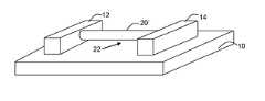
- a insulating carrier 10such as an oxide wafer is provided, onto which a silicon layer is formed and patterned into a source structure 12 , a drain structure 14 and a channel structure 20 wedged between the source structure 12 and the drain structure 14 .
- Source structure 12 , drain structure 14 and channel structure 20may be formed using a conventional FinFET process, with channel structure 20 being the ‘fin’ of the FinFET.
- the finpreferably has a square cross-section since this simplifies the etching process yielding the fin, and improves the quality of the patterned fin.
- a recess 22 formed between the Si channel structure 20 and the insulating carrier 10may be formed by any suitable etching step.
- the oxide carrier 10may be underetched.
- the channel structure 20may comprise a Si/SiGe stack, with the SiGe layer being selectively removed, e.g. by means of a wet etch.
- Such etching stepsare all well known, see for instance E. Saarniletho et al. in ‘Local buried oxide technology for HV transistors integrated in CMOS’, in the proceedings of 19th International Symposium on Power Semiconductor Devices and IC's, 2007. ISPSD '07, 27-31 May 2007, page(s) 81-84, and will therefore not be explained any further.
- the recessed channel structureis converted into a substantially cylindrical channel structure 20 ′.
- Thismay be achieved by any suitable process step, such as a hydrogen annealing step disclosed by Fu-Liang Yang et al., in VLSI, pp. 196-197 (2004), in which such an annealing step was successfully used to form wires having a substantially cylindrical shape.
- a semiconducting layer 30is grown over the substantially cylindrical channel structure 20 ′.
- the semiconducting layer 30may comprise a Si (1 ⁇ x) Ge x layer, preferably with 0 ⁇ x ⁇ 1.
- a relatively high Ge content in this layeris preferred to enhance the quantum well behavior of this layer.
- the Si (1 ⁇ x) Ge x layermay be formed by an epitaxial growth step.
- the epitaxial growing of such layersis well known to the skilled person, and will not be further explained for reasons of brevity only.
- the semiconducting layer 30should preferably not exceed a thickness of 10 nm in order to obtain pronounced quantum confinement effects in this layer.
- a confinement layer 40such as a silicon cap layer is grown around the semiconductor layer 30 .
- the confinement layermay be grown in any suitable way, e.g. by means of an epitaxial growth step.
- the thickness of this cap layershould be only a few nanometers thick, e.g. 2-3 nm, to allow the growth of a high quality oxide layer over this cap layer, and to avoid the formation of parasitic conductive channels.
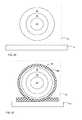
- the quantum well structureis completed by the formation of a conventional all-around gate stack including an oxide layer 50 and the gate layer 60 .
- the oxide layer 50may comprise any suitable material, e.g. a SiO 2 based oxide or a material having a dielectric constant in excess of five, i.e. a high-k dielectric.
- the gate layer 60may comprise any suitable material, e.g. polySi or a metal gate electrode.
- the semiconductor devicemay be completed in any suitable way. For instance, source and drain region formation may proceed in a manner similar to the manufacturing of conventional bulk MOSFETs.
- the cylindrical channel structure 20 ′comprising Si
- the semiconductor layer 30comprising Si (1 ⁇ x) Ge x
- the confinement layer 40comprising Si
- a pMOS-type quantum well deviceis achieved, wherein the cylindrical channel structure 20 ′ acts as a further confinement structure for the Si (1 ⁇ x) Ge x quantum well.
- the corresponding nMOS-type devicemay be formed by altering the above process as follows.
- a SiGe channel structure 20 ′may be formed, followed by growing a strained Si semiconductor layer 30 surrounding the SiGe channel structure 20 ′.
- the strained Si semiconductor layer 30may be covered by a SiGe confinement layer 40 , which may be grown epitaxially or in any other suitable way.
- FIG. 3shows an alternative embodiment of a semiconductor device of the present invention, wherein the inner confinement layer has been omitted.
- the semiconductor layer 30is the innermost structure of the quantum well semiconductor device according to this embodiment of the present invention.
- a pMOS-type device as shown in FIG. 3may be formed by amending the process steps in FIGS. 2A-F as follows. Following the deposition of the Si (1 ⁇ x) Ge x semiconductor layer 30 over the cylindrical Si channel structure 20 ′, the step of depositing the confinement layer 40 is omitted, and the method proceeds to growing the oxide layer 50 over the Si (1 ⁇ x) Ge x semiconductor layer 30 .
- the intermediate deviceis exposed to a thermal budget, which may be during or following the oxidation step, which forces the migration of the Ge atoms from the semiconductor layer 30 towards the substantially cylindrical Si channel structure 20 ′, thereby converting layer 20 ′ into a semiconductor layer 30 ′, and converting original semiconductor layer 30 into a confinement layer 40 .
- the semiconductor layer 30 ′typically will comprise a higher concentration of Ge atoms than the confinement layer 40 . It is emphasized that in this way, a semiconductor layer 30 ′ having high Ge concentrations can be achieved without introducing strain and defects in the semiconductor device.
- the corresponding nMOS-type devicemay be obtained by using the substantially cylindrical Si channel structure 20 ′ as the semiconductor layer, and the Si (1 ⁇ x) Ge x layer 30 as the confinement structure, in which case the deposition of the confinement layer 40 may be omitted from the process depicted in FIGS. 2A-F .
- the band gap misalignment in this deviceis given by the energy gap difference between the Si channel and the SiGe confinement layer.
- the aforementioned quantum well manufacturing processeshave the advantage that they can be implemented using CMOS compatible process steps, and that the process steps are all scalable, such that future submicron devices, e.g. devices having feature sizes well below the 22 nm technology feature sizes, may also be achieved using these processes.
Landscapes
- Engineering & Computer Science (AREA)
- Chemical & Material Sciences (AREA)
- Nanotechnology (AREA)
- Physics & Mathematics (AREA)
- Mathematical Physics (AREA)
- Theoretical Computer Science (AREA)
- Crystallography & Structural Chemistry (AREA)
- Thin Film Transistor (AREA)
- Insulated Gate Type Field-Effect Transistor (AREA)
Abstract
Description
- The present invention relates to a method for manufacturing a semiconductor device, and in particular a gate-all-around (GAA) FinFET device.
- The present invention further relates to a semiconductor device and in particular a GAA FinFET device.
- The continuous scaling of the dimensions of a conventional bulk metal oxide semiconductor field effect transistor (MOSFET) is becoming increasingly difficult due to the uncontrollable short channel effects. Such effects cause a large degradation in the transistor performance, in its switching efficiency as well as in its speed during commutations. For this reason, several alternative transistor designs are being investigated, such as the use of new materials such as high-k dielectric and metal gate materials in conventional transistor designs, and/or the development of alternative transistor architectures.
- A particular architecture that has attracted a lot of attention is the so-called FinFET device, in which a thin fin-shaped channel is provided between a source and drain region on an insulating carrier such as an oxide wafer, with multiple gates controlling the channel conductivity. FinFET devices are considered to be promising due to their excellent intrinsic performance and their high compatibility with the conventional CMOS process, which means that these devices can be manufactured without the need for large investments in new manufacturing equipment.
- One of the key features of FinFET devices is represented by a very high electrostatic integrity compared to conventional transistor architectures. This is due to the additional control over the carriers in the channel exerted by the multi-gate configuration. The presence of two or three gate thus provides a much better control of short channel effects, resulting in high performances and improved scalability compared to conventional transistor designs. A natural extension of a FinFET device is represented by the gate-all-around (GAA) device, in which a gate structure envelopes the fin-shaped channel. This further improves control over short channel effects. An example of such a device is disclosed in U.S. patent application No. U.S. 2007/0145431.
- The downscaling of transistor dimensions has further initiated interest in designing devices that exhibit quantization effects, such as transistors based on quantum wires. U.S. patent application No. 2008/0014689 discloses a gate-all-around planar nanowire semiconductor device, in which the planar nanowires are formed between a source and a drain over an insulating layer of a semiconductor substrate, with a gate stack being grown all-around the planar nanowires. The gate stack is subsequently etched and patterned. During this process, the planar nanowires are severed between the gate and the source, and between the gate and the drain, leaving portions of the gate-all-around planar nanowires remain between the source and the drain and serve as the active region of the channel. The remaining gate-all-around planar nanowires are epitaxially regrown to reconnect to the source and the drain.
- This device has several drawbacks. The manufacturing process is relatively complex, and results in a semiconductor nanowire having a planar shape, rather than a cylindrical shape facilitating optimization of the quantization effects.
- The present invention seeks to provide a method of manufacturing a semiconductor device having a cylindrically shaped channel with a surrounding gate.
- The present invention further seeks to provide a semiconductor device having a cylindrically shaped channel with a surrounding gate.
- According to a first aspect of the present invention, there is provided a method of manufacturing a semiconductor device, comprising providing an insulating carrier; providing a channel structure between a source structure and a drain structure on said carrier; selectively removing a part of the channel structure, thereby forming a recess between the channel and the carrier; exposing the device to an annealing step such that the channel structure obtains a substantially cylindrical shape; forming a confinement layer surrounding the substantially cylindrical channel structure; growing an oxide layer surrounding the confinement layer; and forming a gate structure surrounding the oxide layer.
- The method of the present invention allows for the formation of a cylindrical channel structure using conventional CMOS processing steps. For instance, the combined channel, source and drain structures may be a FinFET structure. The confinement layer, i.e. layer having a larger band gap than the semiconductor layer of the quantum wire, ensures that charge carriers are confined in the cylindrical channel structure, thus creating a quantum wire.
- In an embodiment, the method further comprises growing a semiconducting layer surrounding the substantially cylindrical channel structure prior to forming the confinement layer, and wherein the confinement layer surrounds the substantially cylindrical channel structure and the semiconducting layer, the substantially cylindrical channel acting as a further confinement layer for the semiconducting layer. This creates a quantum well structure in between an inner and an outer confinement structure. This further improves the efficiency of the quantum confinement, and thus aids in reducing the occurrence of charge carriers at the surface of the wire. The semiconducting layer may be grown epitaxially.
- The channel structure formed on the insulating carrier has a square cross section. This has the advantage over e.g. a conventional FinFET process that the channel structure may be more easily formed, thus reducing process complexity. Moreover, it has been found that the use of a channel structure having a square cross section yields a device having improved characteristics compared to devices formed in a conventional FinFET process.
- The above method may be used to form both nMOS and pMOS type devices, thus facilitating the manufacture of integrated circuits (ICs) comprising the inventive semiconductor devices through conventional CMOS processes.
- In an embodiment, the channel structure is a silicon channel structure, and the step of forming a confinement layer comprises growing a silicon/germanium (SiGe) layer surrounding the substantially cylindrical channel structure; and growing the oxide layer surrounding the SiGe layer at a predefined temperature, said predefined temperature facilitating the migration of Ge atoms from the SiGe layer towards the substantially cylindrical channel structure, thereby converting the SiGe layer into the confinement layer. This embodiment yields a p-type quantum well for transporting holes between the source and drain regions.
- The complementary n-type device may be achieved by an embodiment wherein the channel is a strained silicon channel structure, and wherein forming the confinement layer comprises epitaxially growing a SiGe layer. Instead of strained silicon, suitable group III-V materials may be used for the semiconductor quantum well of the n-type device.
- A p-type device having a quantum well sandwiched between two confinement structures may be achieved when the channel structure is a silicon channel structure, wherein growing a semiconducting layer comprises epitaxially growing a SiGe layer; and forming the confinement layer comprises epitaxially growing a silicon layer surrounding the SiGe layer. Such a device has a two-layer core structure, comprising an inner confinement silicon structure enveloped by a SiGe semiconductor quantum well.
- The corresponding n-type device may be formed when the channel structure is a SiGe channel structure, wherein growing a semiconducting layer comprises growing a strained silicon layer; and forming the confinement layer comprises epitaxially growing a SiGe layer surrounding the strained silicon layer.
- According to another aspect of the present invention, there is provided a semiconductor device on an insulating carrier, the device comprising a source region, a drain region, and a channel structure between the source region and the drain region, the channel structure comprising a substantially cylindrical core structure comprising a semiconducting material; a confinement layer surrounding the core structure; an oxide layer surrounding the confinement layer; and a gate structure surrounding the oxide layer. Such a device, which is manufactured by the method of the present invention, has excellent conductive properties and a controllable short channel effects, and can be manufactured using conventional CMOS process techniques.
- In an embodiment, the core structure comprises a further confinement structure surrounded by a layer of the semiconducting material, thus achieving a quantum well sandwiched between two confinement structures. The semiconducting material of these semiconductor devices may be silicon/germanium and the confinement structure(s) may comprise silicon in case of p-type devices. The semiconducting material may be strained silicon and the confinement structure(s) may comprise silicon/germanium in case of n-type devices. Alternatively, the n-type devices may comprise a suitable group III-V material as semiconductor material.
- Embodiments of the invention are described in more detail and by way of non-limiting examples with reference to the accompanying drawings, wherein
FIG. 1 schematically depicts the principle of a quantum well device;FIGS. 2A-F schematically depict key steps of an embodiment of a method of manufacturing a semiconductor device in accordance with an embodiment of the present invention; andFIG. 3 schematically depicts a semiconductor device manufactured in accordance with an alternative embodiment of the present invention.- It should be understood that the Figures are merely schematic and are not drawn to scale. It should also be understood that the same reference numerals are used throughout the Figures to indicate the same or similar parts.
FIG. 1 schematically depicts the concept of a cylindrical quantum well. Such wells are sometimes also referred to as quantum wires. In this particular case, an inner region II, e.g. a Ge cylindrical channel, is sandwiched between two regions I, e.g. an inner and an outer silicon layer. The region II is used as a charge transport layer, e.g. a holes transport layer. A quantum well is formed in region II due to the difference in energy gaps between the valence band (VB) and the conduction band (CB) splitting for regions I and region II respectively. As a result, charge carriers, e.g. holes, are confined inside the quantum well. In other words, regions I act as confinement layers to confine the charge carriers to region II. The large sub-band splitting observed in the quantum well, wherein the valence band level may be raised to above the Fermi level (EF), largely reduces intra-sub-band scattering events. Consequently, the carrier mobility and the current drive capability of the device is increased. In case of region II comprising Ge or SiGe and regions I comprising Si, a pMOS device may be obtained. An nMOS device may be achieved by sandwiching a strained Si layer between two SiGe layers. Alternatives to strained Si include suitable group III-V materials, or combinations thereof.- One of the advantages of such a cylindrical quantum well structure is the potential to achieve ballistic transport behavior. Such behavior has already been demonstrated for Ge/Si nanowires by Jie Xiang at al. in Nature, pp. 489-493 (2005). A drawback of this device is that its manufacturing cannot be achieved with conventional CMOS processes, but requires a highly experimental technology based on growing nanowires instead.
- A further advantage is that the lack of dopants in the channel and the large sub-band splitting obtained as a consequence of the two-dimensional quantum confinement allow for a substantial increase of the mean free path in the device. A mean free path larger than 500 nm has been already experimentally demonstrated in the aforementioned publication by Jie Xiang at al. Even in case the transport of charge carriers through region II is collision dominated, the device performance is improved by the high charge carrier mobility at low and high field. Indeed, as a consequence of the large sub-band splitting, the inter-sub-band scattering is largely reduced. Therefore, few sub-bands participate effectively to the transport and hence high mobility is expected.
- Such a device is further characterized by a higher immunity to surface states with respect to planar equivalent such as disclosed in U.S. patent application No. 2008/0014689. The cylindrical nature of the transistor and the radial quantum confinement induce a conducting channel in the centre of the cylinder, i.e. far away from the cylinder surface. This greatly reduces the occurrence of scattering events due to collisions with impurities at the surface, thus greatly improving the device mobility. The reduced diameter of the conducting channel, e.g. a SiGe channel, as well as of the confinement layer, e.g. a Si cap layer, allow for an increase in the Ge concentration in region II without introducing strain in the device.
FIGS. 2A-F schematically depict a method of manufacturing such a device using CMOS compatible processing techniques. InFIG. 2A , a insulatingcarrier 10 such as an oxide wafer is provided, onto which a silicon layer is formed and patterned into asource structure 12, adrain structure 14 and achannel structure 20 wedged between thesource structure 12 and thedrain structure 14.Source structure 12,drain structure 14 andchannel structure 20 may be formed using a conventional FinFET process, withchannel structure 20 being the ‘fin’ of the FinFET.- Many suitable CMOS compatible processes for manufacturing such a FinFET structure are well-known to the skilled person, and are therefore not further explained for reasons of brevity only. It is however emphasized that in contrast to the conventional FinFET manufacturing processes, the high aspect-ratio which characterizes conventional FinFET devices is not necessary for the semiconductor device of the present invention. In fact, the fin preferably has a square cross-section since this simplifies the etching process yielding the fin, and improves the quality of the patterned fin.
- In
FIG. 2B , arecess 22 formed between theSi channel structure 20 and the insulatingcarrier 10. Such arecess 22 may be formed by any suitable etching step. For instance, theoxide carrier 10 may be underetched. Alternatively, thechannel structure 20 may comprise a Si/SiGe stack, with the SiGe layer being selectively removed, e.g. by means of a wet etch. Such etching steps are all well known, see for instance E. Saarniletho et al. in ‘Local buried oxide technology for HV transistors integrated in CMOS’, in the proceedings of 19th International Symposium on Power Semiconductor Devices and IC's, 2007. ISPSD '07, 27-31 May 2007, page(s) 81-84, and will therefore not be explained any further. - In
FIG. 2C , the recessed channel structure is converted into a substantiallycylindrical channel structure 20′. This may be achieved by any suitable process step, such as a hydrogen annealing step disclosed by Fu-Liang Yang et al., in VLSI, pp. 196-197 (2004), in which such an annealing step was successfully used to form wires having a substantially cylindrical shape. - In
FIG. 2D , which depicts the cross section ofchannel structure 20′ as seen throughsource region 12, asemiconducting layer 30 is grown over the substantiallycylindrical channel structure 20′. For example, thesemiconducting layer 30 may comprise a Si(1−x)Gexlayer, preferably with 0<<x<1. A relatively high Ge content in this layer is preferred to enhance the quantum well behavior of this layer. Preferably, x is in the area of 0.3-0.4. It has been found that this range allows for the enhancement the band gap splitting between thesemiconducting layer 30 and the surrounding confinement layer(s) without introducing strain into the semiconductor device. It has been found that the cylindrical shape of this layer allows for a higher Ge content in this layer without introduction of strain than compared to prior art solutions in which planar SiGe layers are used, where the maximum fraction of Ge was typically limited to x=0.2. - The Si(1−x)Gexlayer may be formed by an epitaxial growth step. The epitaxial growing of such layers is well known to the skilled person, and will not be further explained for reasons of brevity only.
- The
semiconducting layer 30 should preferably not exceed a thickness of 10 nm in order to obtain pronounced quantum confinement effects in this layer. - In
FIG. 2E , aconfinement layer 40 such as a silicon cap layer is grown around thesemiconductor layer 30. The confinement layer may be grown in any suitable way, e.g. by means of an epitaxial growth step. Preferably, the thickness of this cap layer should be only a few nanometers thick, e.g. 2-3 nm, to allow the growth of a high quality oxide layer over this cap layer, and to avoid the formation of parasitic conductive channels. - In
FIG. 2F , the quantum well structure is completed by the formation of a conventional all-around gate stack including anoxide layer 50 and thegate layer 60. Theoxide layer 50 may comprise any suitable material, e.g. a SiO2based oxide or a material having a dielectric constant in excess of five, i.e. a high-k dielectric. Thegate layer 60 may comprise any suitable material, e.g. polySi or a metal gate electrode. The semiconductor device may be completed in any suitable way. For instance, source and drain region formation may proceed in a manner similar to the manufacturing of conventional bulk MOSFETs. - In case of the
cylindrical channel structure 20′ comprising Si, thesemiconductor layer 30 comprising Si(1−x)Gexand theconfinement layer 40 comprising Si, a pMOS-type quantum well device is achieved, wherein thecylindrical channel structure 20′ acts as a further confinement structure for the Si(1−x)Gexquantum well. - The corresponding nMOS-type device may be formed by altering the above process as follows. A
SiGe channel structure 20′ may be formed, followed by growing a strainedSi semiconductor layer 30 surrounding theSiGe channel structure 20′. The strainedSi semiconductor layer 30 may be covered by aSiGe confinement layer 40, which may be grown epitaxially or in any other suitable way. FIG. 3 shows an alternative embodiment of a semiconductor device of the present invention, wherein the inner confinement layer has been omitted. Hence, thesemiconductor layer 30 is the innermost structure of the quantum well semiconductor device according to this embodiment of the present invention.- A pMOS-type device as shown in
FIG. 3 may be formed by amending the process steps inFIGS. 2A-F as follows. Following the deposition of the Si(1−x)Gexsemiconductor layer30 over the cylindricalSi channel structure 20′, the step of depositing theconfinement layer 40 is omitted, and the method proceeds to growing theoxide layer 50 over the Si(1−x)Gexsemiconductor layer30. The intermediate device is exposed to a thermal budget, which may be during or following the oxidation step, which forces the migration of the Ge atoms from thesemiconductor layer 30 towards the substantially cylindricalSi channel structure 20′, thereby convertinglayer 20′ into asemiconductor layer 30′, and convertingoriginal semiconductor layer 30 into aconfinement layer 40. Thesemiconductor layer 30′ typically will comprise a higher concentration of Ge atoms than theconfinement layer 40. It is emphasized that in this way, asemiconductor layer 30′ having high Ge concentrations can be achieved without introducing strain and defects in the semiconductor device. - The corresponding nMOS-type device may be obtained by using the substantially cylindrical
Si channel structure 20′ as the semiconductor layer, and the Si(1−x)Gexlayer30 as the confinement structure, in which case the deposition of theconfinement layer 40 may be omitted from the process depicted inFIGS. 2A-F . For such an nMOS-type device, it is preferable to limit the Ge concentration in the Si(1−x)Gexlayer, e.g. x≦0.2, to ensure that a high quality gate stack may be formed over this layer. The band gap misalignment in this device is given by the energy gap difference between the Si channel and the SiGe confinement layer. The energy gap of pure Ge is roughly half of the energy gap of silicon and, as a crude approximation, the energy gap of a Si(1−x)Ge(x)layer may be obtained as a linear interpolation between the absolute band gap values for pure Si (i.e. x=1) and pure Ge (i.e. x=0) for the considered x mole fraction. It will be appreciated that to ensure that a sufficient band gap misalignment between the Sisemiconducting channel 30 and theSiGe confinement layer 40 remains, x should be substantially larger than 0, e.g. 0.1×0.2 for this embodiment. - The aforementioned quantum well manufacturing processes have the advantage that they can be implemented using CMOS compatible process steps, and that the process steps are all scalable, such that future submicron devices, e.g. devices having feature sizes well below the 22 nm technology feature sizes, may also be achieved using these processes.
- It should be noted that the above-mentioned embodiments illustrate rather than limit the invention, and that those skilled in the art will be able to design many alternative embodiments without departing from the scope of the appended claims. In the claims, any reference signs placed between parentheses shall not be construed as limiting the claim. The word “comprising” does not exclude the presence of elements or steps other than those listed in a claim. The word “a” or “an” preceding an element does not exclude the presence of a plurality of such elements. The invention can be implemented by means of hardware comprising several distinct elements. In the device claim enumerating several means, several of these means can be embodied by one and the same item of hardware. The mere fact that certain measures are recited in mutually different dependent claims does not indicate that a combination of these measures cannot be used to advantage.
Claims (14)
Applications Claiming Priority (3)
| Application Number | Priority Date | Filing Date | Title |
|---|---|---|---|
| EP08102004 | 2008-02-26 | ||
| EP08102004.2 | 2008-02-26 | ||
| PCT/IB2009/050641WO2009107031A1 (en) | 2008-02-26 | 2009-02-17 | Method for manufacturing semiconductor device and semiconductor device |
Publications (1)
| Publication Number | Publication Date |
|---|---|
| US20110018065A1true US20110018065A1 (en) | 2011-01-27 |
Family
ID=40766047
Family Applications (1)
| Application Number | Title | Priority Date | Filing Date |
|---|---|---|---|
| US12/918,398AbandonedUS20110018065A1 (en) | 2008-02-26 | 2009-02-17 | Method for manufacturing semiconductor device and semiconductor device |
Country Status (4)
| Country | Link |
|---|---|
| US (1) | US20110018065A1 (en) |
| EP (1) | EP2257974A1 (en) |
| CN (1) | CN101960570A (en) |
| WO (1) | WO2009107031A1 (en) |
Cited By (45)
| Publication number | Priority date | Publication date | Assignee | Title |
|---|---|---|---|---|
| US20110024794A1 (en)* | 2009-07-31 | 2011-02-03 | Taiwan Semiconductor Manufacturing Company, Ltd. | Fin structure for high mobility multiple-gate transistor |
| US20110049613A1 (en)* | 2009-09-01 | 2011-03-03 | Taiwan Semiconductor Manufacturing Company, Ltd. | Accumulation type finfet, circuits and fabrication method thereof |
| US20110068407A1 (en)* | 2009-09-24 | 2011-03-24 | Taiwan Semiconductor Manufacturing Company, Ltd. | Germanium FinFETs with Metal Gates and Stressors |
| US8264021B2 (en) | 2009-10-01 | 2012-09-11 | Taiwan Semiconductor Manufacturing Company, Ltd. | Finfets and methods for forming the same |
| US8298925B2 (en) | 2010-11-08 | 2012-10-30 | Taiwan Semiconductor Manufacturing Company, Ltd. | Mechanisms for forming ultra shallow junction |
| US8305790B2 (en) | 2009-03-16 | 2012-11-06 | Taiwan Semiconductor Manufacturing Company, Ltd. | Electrical anti-fuse and related applications |
| US8305829B2 (en) | 2009-02-23 | 2012-11-06 | Taiwan Semiconductor Manufacturing Company, Ltd. | Memory power gating circuit for controlling internal voltage of a memory array, system and method for controlling the same |
| US20130056795A1 (en)* | 2011-09-06 | 2013-03-07 | Taiwan Semiconductor Manufacturing Company, Ltd. | FinFET Design Controlling Channel Thickness |
| US8431453B2 (en) | 2011-03-31 | 2013-04-30 | Taiwan Semiconductor Manufacturing Company, Ltd. | Plasma doping to reduce dielectric loss during removal of dummy layers in a gate structure |
| US8440517B2 (en) | 2010-10-13 | 2013-05-14 | Taiwan Semiconductor Manufacturing Company, Ltd. | FinFET and method of fabricating the same |
| US8461015B2 (en) | 2009-07-08 | 2013-06-11 | Taiwan Semiconductor Manufacturing Company, Ltd. | STI structure and method of forming bottom void in same |
| US8472227B2 (en) | 2010-01-27 | 2013-06-25 | Taiwan Semiconductor Manufacturing Company, Ltd. | Integrated circuits and methods for forming the same |
| US8482073B2 (en) | 2010-03-25 | 2013-07-09 | Taiwan Semiconductor Manufacturing Company, Ltd. | Integrated circuit including FINFETs and methods for forming the same |
| US8497528B2 (en) | 2010-05-06 | 2013-07-30 | Taiwan Semiconductor Manufacturing Company, Ltd. | Method for fabricating a strained structure |
| US8592915B2 (en) | 2011-01-25 | 2013-11-26 | Taiwan Semiconductor Manufacturing Company, Ltd. | Doped oxide for shallow trench isolation (STI) |
| US8603924B2 (en) | 2010-10-19 | 2013-12-10 | Taiwan Semiconductor Manufacturing Company, Ltd. | Methods of forming gate dielectric material |
| US8623728B2 (en) | 2009-07-28 | 2014-01-07 | Taiwan Semiconductor Manufacturing Company, Ltd. | Method for forming high germanium concentration SiGe stressor |
| US8759943B2 (en) | 2010-10-08 | 2014-06-24 | Taiwan Semiconductor Manufacturing Company, Ltd. | Transistor having notched fin structure and method of making the same |
| US8769446B2 (en) | 2010-11-12 | 2014-07-01 | Taiwan Semiconductor Manufacturing Company, Ltd. | Method and device for increasing fin device density for unaligned fins |
| US8877602B2 (en) | 2011-01-25 | 2014-11-04 | Taiwan Semiconductor Manufacturing Company, Ltd. | Mechanisms of doping oxide for forming shallow trench isolation |
| US8912602B2 (en) | 2009-04-14 | 2014-12-16 | Taiwan Semiconductor Manufacturing Company, Ltd. | FinFETs and methods for forming the same |
| US8957482B2 (en) | 2009-03-31 | 2015-02-17 | Taiwan Semiconductor Manufacturing Company, Ltd. | Electrical fuse and related applications |
| US8980719B2 (en) | 2010-04-28 | 2015-03-17 | Taiwan Semiconductor Manufacturing Company, Ltd. | Methods for doping fin field-effect transistors |
| DE112011103810B4 (en)* | 2011-05-26 | 2015-05-13 | Peking University | Production process for surround-gate silicon nanowire transistor with air as a spacer |
| DE102013223263A1 (en) | 2013-11-14 | 2015-05-21 | Globalfoundries Inc. | Nanowire transistor component |
| US9040393B2 (en) | 2010-01-14 | 2015-05-26 | Taiwan Semiconductor Manufacturing Company, Ltd. | Method of forming semiconductor structure |
| US9048181B2 (en) | 2010-11-08 | 2015-06-02 | Taiwan Semiconductor Manufacturing Company, Ltd. | Mechanisms for forming ultra shallow junction |
| US20150187947A1 (en)* | 2013-04-26 | 2015-07-02 | Globalfoundries Inc. | Finfet with active region shaped structures and channel separation |
| JP2015122488A (en)* | 2013-12-20 | 2015-07-02 | アイメックImec | Transistor device manufacturing method and related devices |
| US9190505B2 (en) | 2012-12-28 | 2015-11-17 | Renesas Electronics Corporation | Field effect transistor with channel core modified for a backgate bias and method of fabrication |
| US20160104799A1 (en)* | 2014-10-10 | 2016-04-14 | Globalfoundries Inc. | Dual-strained nanowire and finfet devices with dielectric isolation |
| US9331146B2 (en) | 2014-06-11 | 2016-05-03 | International Business Machines Corporation | Silicon nanowire formation in replacement metal gate process |
| US20160260621A1 (en)* | 2009-09-28 | 2016-09-08 | Semiconductor Manufacturing International (Shanghai) Corporation | System and method for integrated circuits with cylindrical gate structures |
| US20160268172A1 (en)* | 2013-08-26 | 2016-09-15 | Taiwan Semiconductor Manufacturing Company, Ltd. | Integrate Circuit with Nanowires |
| US9484462B2 (en) | 2009-09-24 | 2016-11-01 | Taiwan Semiconductor Manufacturing Company, Ltd. | Fin structure of fin field effect transistor |
| DE112011106004B4 (en)* | 2011-12-23 | 2017-07-13 | Intel Corporation | Semiconductor structure and method of fabricating a CMOS nanowire semiconductor structure |
| US9735176B2 (en)* | 2015-12-30 | 2017-08-15 | International Business Machines Corporation | Stacked nanowires with multi-threshold voltage solution for PFETS |
| US10381479B2 (en) | 2017-07-28 | 2019-08-13 | International Business Machines Corporation | Interface charge reduction for SiGe surface |
| US10497719B2 (en) | 2017-11-16 | 2019-12-03 | Samsung Electronics Co., Ltd. | Method for selectively increasing silicon fin area for vertical field effect transistors |
| US10553718B2 (en)* | 2014-03-14 | 2020-02-04 | Taiwan Semiconductor Manufacturing Co., Ltd. | Semiconductor devices with core-shell structures |
| US10693008B2 (en)* | 2013-09-27 | 2020-06-23 | Intel Corporation | Cladding layer epitaxy via template engineering for heterogeneous integration on silicon |
| US10916544B2 (en)* | 2018-09-28 | 2021-02-09 | Sien (Qingdao) Integrated Circuits Co., Ltd | Gate-all-around quantum well complementary inverter and method of making the same |
| US11081592B2 (en)* | 2016-12-15 | 2021-08-03 | Taiwan Semiconductor Manufacturing Co., Ltd. | Semiconductor device and manufacturing method thereof |
| US20230178658A1 (en)* | 2021-12-02 | 2023-06-08 | Intel Corporation | Recessed inner gate spacers and partial replacement channel in non-planar transistors |
| US11799035B2 (en)* | 2019-04-12 | 2023-10-24 | The Research Foundation For The State University Of New York | Gate all-around field effect transistors including quantum-based features |
Families Citing this family (7)
| Publication number | Priority date | Publication date | Assignee | Title |
|---|---|---|---|---|
| US20110049473A1 (en)* | 2009-08-28 | 2011-03-03 | International Business Machines Corporation | Film Wrapped NFET Nanowire |
| US8680510B2 (en)* | 2010-06-28 | 2014-03-25 | International Business Machines Corporation | Method of forming compound semiconductor |
| CN103915316B (en)* | 2013-01-09 | 2018-07-27 | 中国科学院微电子研究所 | Stacked nanowire fabrication method |
| CN104253048B (en)* | 2013-06-28 | 2019-03-15 | 中国科学院微电子研究所 | Stacked nanowire fabrication method |
| US9917169B2 (en)* | 2014-07-02 | 2018-03-13 | Taiwan Semiconductor Manufacturing Company Limited | Semiconductor device and method of formation |
| US9425324B2 (en)* | 2014-09-30 | 2016-08-23 | Taiwan Semiconductor Manufacturing Company Limited | Semiconductor device and channel structure thereof |
| CN104392917B (en)* | 2014-11-17 | 2017-09-29 | 上海集成电路研发中心有限公司 | A kind of forming method of all-around-gate structure |
Citations (13)
| Publication number | Priority date | Publication date | Assignee | Title |
|---|---|---|---|---|
| US5146117A (en)* | 1991-04-01 | 1992-09-08 | Hughes Aircraft Company | Convertible multi-function microelectronic logic gate structure and method of fabricating the same |
| US20020149031A1 (en)* | 2001-04-12 | 2002-10-17 | Samsung Electronics Co., Ltd. | Semiconductor device having gate all around type transistor and method of forming the same |
| US20030089899A1 (en)* | 2000-08-22 | 2003-05-15 | Lieber Charles M. | Nanoscale wires and related devices |
| US20040166642A1 (en)* | 2003-02-20 | 2004-08-26 | Hao-Yu Chen | Semiconductor nano-rod devices |
| US20050017377A1 (en)* | 2003-07-21 | 2005-01-27 | International Business Machines Corporation | FET channel having a strained lattice structure along multiple surfaces |
| US20050064185A1 (en)* | 2003-08-04 | 2005-03-24 | Nanosys, Inc. | System and process for producing nanowire composites and electronic substrates therefrom |
| US20050227435A1 (en)* | 2004-04-12 | 2005-10-13 | Samsung Electronics Co., Ltd. | Non-volatile memory devices and method for forming the same |
| US20050275010A1 (en)* | 2004-06-10 | 2005-12-15 | Hung-Wei Chen | Semiconductor nano-wire devices and methods of fabrication |
| US20060052947A1 (en)* | 2004-05-17 | 2006-03-09 | Evelyn Hu | Biofabrication of transistors including field effect transistors |
| US20060216897A1 (en)* | 2005-03-24 | 2006-09-28 | Samsung Electronics Co., Ltd. | Semiconductor device having a round-shaped nano-wire transistor channel and method of manufacturing same |
| US20070029586A1 (en)* | 2005-08-08 | 2007-02-08 | Freescale Semiconductor, Inc. | Multi-channel transistor structure and method of making thereof |
| US20070145431A1 (en)* | 2005-12-24 | 2007-06-28 | Samsung Electronics Co., Ltd. | Fin-FET having GAA structure and methods of fabricating the same |
| US20080014689A1 (en)* | 2006-07-07 | 2008-01-17 | Texas Instruments Incorporated | Method for making planar nanowire surround gate mosfet |
Family Cites Families (1)
| Publication number | Priority date | Publication date | Assignee | Title |
|---|---|---|---|---|
| TW554388B (en)* | 2001-03-30 | 2003-09-21 | Univ California | Methods of fabricating nanostructures and nanowires and devices fabricated therefrom |
- 2009
- 2009-02-17USUS12/918,398patent/US20110018065A1/ennot_activeAbandoned
- 2009-02-17CNCN200980106290.5Apatent/CN101960570A/enactivePending
- 2009-02-17EPEP09714517Apatent/EP2257974A1/ennot_activeWithdrawn
- 2009-02-17WOPCT/IB2009/050641patent/WO2009107031A1/enactiveApplication Filing
Patent Citations (16)
| Publication number | Priority date | Publication date | Assignee | Title |
|---|---|---|---|---|
| US5146117A (en)* | 1991-04-01 | 1992-09-08 | Hughes Aircraft Company | Convertible multi-function microelectronic logic gate structure and method of fabricating the same |
| US7301199B2 (en)* | 2000-08-22 | 2007-11-27 | President And Fellows Of Harvard College | Nanoscale wires and related devices |
| US20030089899A1 (en)* | 2000-08-22 | 2003-05-15 | Lieber Charles M. | Nanoscale wires and related devices |
| US20020149031A1 (en)* | 2001-04-12 | 2002-10-17 | Samsung Electronics Co., Ltd. | Semiconductor device having gate all around type transistor and method of forming the same |
| US20040166642A1 (en)* | 2003-02-20 | 2004-08-26 | Hao-Yu Chen | Semiconductor nano-rod devices |
| US6855606B2 (en)* | 2003-02-20 | 2005-02-15 | Taiwan Semiconductor Manufacturing Company, Ltd. | Semiconductor nano-rod devices |
| US20050121706A1 (en)* | 2003-02-20 | 2005-06-09 | Hao-Yu Chen | Semiconductor nano-rod devices |
| US20050017377A1 (en)* | 2003-07-21 | 2005-01-27 | International Business Machines Corporation | FET channel having a strained lattice structure along multiple surfaces |
| US20050064185A1 (en)* | 2003-08-04 | 2005-03-24 | Nanosys, Inc. | System and process for producing nanowire composites and electronic substrates therefrom |
| US20050227435A1 (en)* | 2004-04-12 | 2005-10-13 | Samsung Electronics Co., Ltd. | Non-volatile memory devices and method for forming the same |
| US20060052947A1 (en)* | 2004-05-17 | 2006-03-09 | Evelyn Hu | Biofabrication of transistors including field effect transistors |
| US20050275010A1 (en)* | 2004-06-10 | 2005-12-15 | Hung-Wei Chen | Semiconductor nano-wire devices and methods of fabrication |
| US20060216897A1 (en)* | 2005-03-24 | 2006-09-28 | Samsung Electronics Co., Ltd. | Semiconductor device having a round-shaped nano-wire transistor channel and method of manufacturing same |
| US20070029586A1 (en)* | 2005-08-08 | 2007-02-08 | Freescale Semiconductor, Inc. | Multi-channel transistor structure and method of making thereof |
| US20070145431A1 (en)* | 2005-12-24 | 2007-06-28 | Samsung Electronics Co., Ltd. | Fin-FET having GAA structure and methods of fabricating the same |
| US20080014689A1 (en)* | 2006-07-07 | 2008-01-17 | Texas Instruments Incorporated | Method for making planar nanowire surround gate mosfet |
Non-Patent Citations (1)
| Title |
|---|
| American Heritage Dictionary definition of cylindrical.* |
Cited By (86)
| Publication number | Priority date | Publication date | Assignee | Title |
|---|---|---|---|---|
| US8305829B2 (en) | 2009-02-23 | 2012-11-06 | Taiwan Semiconductor Manufacturing Company, Ltd. | Memory power gating circuit for controlling internal voltage of a memory array, system and method for controlling the same |
| US8305790B2 (en) | 2009-03-16 | 2012-11-06 | Taiwan Semiconductor Manufacturing Company, Ltd. | Electrical anti-fuse and related applications |
| US8957482B2 (en) | 2009-03-31 | 2015-02-17 | Taiwan Semiconductor Manufacturing Company, Ltd. | Electrical fuse and related applications |
| US8912602B2 (en) | 2009-04-14 | 2014-12-16 | Taiwan Semiconductor Manufacturing Company, Ltd. | FinFETs and methods for forming the same |
| US8461015B2 (en) | 2009-07-08 | 2013-06-11 | Taiwan Semiconductor Manufacturing Company, Ltd. | STI structure and method of forming bottom void in same |
| US8623728B2 (en) | 2009-07-28 | 2014-01-07 | Taiwan Semiconductor Manufacturing Company, Ltd. | Method for forming high germanium concentration SiGe stressor |
| US9660082B2 (en) | 2009-07-28 | 2017-05-23 | Taiwan Semiconductor Manufacturing Company, Ltd. | Integrated circuit transistor structure with high germanium concentration SiGe stressor |
| US20110024794A1 (en)* | 2009-07-31 | 2011-02-03 | Taiwan Semiconductor Manufacturing Company, Ltd. | Fin structure for high mobility multiple-gate transistor |
| US8629478B2 (en)* | 2009-07-31 | 2014-01-14 | Taiwan Semiconductor Manufacturing Company, Ltd. | Fin structure for high mobility multiple-gate transistor |
| US8896055B2 (en) | 2009-09-01 | 2014-11-25 | Taiwan Semiconductor Manufacturing Company, Ltd. | Accumulation type FinFET, circuits and fabrication method thereof |
| US20110049613A1 (en)* | 2009-09-01 | 2011-03-03 | Taiwan Semiconductor Manufacturing Company, Ltd. | Accumulation type finfet, circuits and fabrication method thereof |
| US8264032B2 (en) | 2009-09-01 | 2012-09-11 | Taiwan Semiconductor Manufacturing Company, Ltd. | Accumulation type FinFET, circuits and fabrication method thereof |
| US9484462B2 (en) | 2009-09-24 | 2016-11-01 | Taiwan Semiconductor Manufacturing Company, Ltd. | Fin structure of fin field effect transistor |
| US10355108B2 (en) | 2009-09-24 | 2019-07-16 | Taiwan Semiconductor Manufacturing Company, Ltd. | Method of forming a fin field effect transistor comprising two etching steps to define a fin structure |
| US9245805B2 (en)* | 2009-09-24 | 2016-01-26 | Taiwan Semiconductor Manufacturing Company, Ltd. | Germanium FinFETs with metal gates and stressors |
| US11158725B2 (en) | 2009-09-24 | 2021-10-26 | Taiwan Semiconductor Manufacturing Company, Ltd. | Fin structure of fin field effect transistor |
| US9698060B2 (en) | 2009-09-24 | 2017-07-04 | Taiwan Semiconductor Manufacturing Company, Ltd. | Germanium FinFETs with metal gates and stressors |
| US20110068407A1 (en)* | 2009-09-24 | 2011-03-24 | Taiwan Semiconductor Manufacturing Company, Ltd. | Germanium FinFETs with Metal Gates and Stressors |
| US9673060B2 (en)* | 2009-09-28 | 2017-06-06 | Semiconductor Manufacturing International (Shanghai) Corporation | System and method for integrated circuits with cylindrical gate structures |
| US20160260621A1 (en)* | 2009-09-28 | 2016-09-08 | Semiconductor Manufacturing International (Shanghai) Corporation | System and method for integrated circuits with cylindrical gate structures |
| US8264021B2 (en) | 2009-10-01 | 2012-09-11 | Taiwan Semiconductor Manufacturing Company, Ltd. | Finfets and methods for forming the same |
| US9040393B2 (en) | 2010-01-14 | 2015-05-26 | Taiwan Semiconductor Manufacturing Company, Ltd. | Method of forming semiconductor structure |
| US9922827B2 (en) | 2010-01-14 | 2018-03-20 | Taiwan Semiconductor Manufacturing Company, Ltd. | Method of forming a semiconductor structure |
| US8472227B2 (en) | 2010-01-27 | 2013-06-25 | Taiwan Semiconductor Manufacturing Company, Ltd. | Integrated circuits and methods for forming the same |
| US8482073B2 (en) | 2010-03-25 | 2013-07-09 | Taiwan Semiconductor Manufacturing Company, Ltd. | Integrated circuit including FINFETs and methods for forming the same |
| US8980719B2 (en) | 2010-04-28 | 2015-03-17 | Taiwan Semiconductor Manufacturing Company, Ltd. | Methods for doping fin field-effect transistors |
| US9450097B2 (en) | 2010-04-28 | 2016-09-20 | Taiwan Semiconductor Manufacturing Company, Ltd. | Methods for doping Fin field-effect transistors and Fin field-effect transistor |
| US9209280B2 (en) | 2010-04-28 | 2015-12-08 | Taiwan Semiconductor Manufacturing Company, Ltd. | Methods for doping fin field-effect transistors |
| US8497528B2 (en) | 2010-05-06 | 2013-07-30 | Taiwan Semiconductor Manufacturing Company, Ltd. | Method for fabricating a strained structure |
| US11251303B2 (en) | 2010-05-06 | 2022-02-15 | Taiwan Semiconductor Manufacturing Company, Ltd. | Method for fabricating a strained structure and structure formed |
| US12356674B2 (en) | 2010-05-06 | 2025-07-08 | Taiwan Semiconductor Manufacturing Company, Ltd. | Method for fabricating a strained structure and structure formed |
| US9147594B2 (en) | 2010-05-06 | 2015-09-29 | Taiwan Semiconductor Manufacturing Company, Ltd. | Method for fabricating a strained structure |
| US11855210B2 (en) | 2010-05-06 | 2023-12-26 | Taiwan Semiconductor Manufacturing Company, Ltd. | Method for fabricating a strained structure and structure formed |
| US10998442B2 (en) | 2010-05-06 | 2021-05-04 | Taiwan Semiconductor Manufacturing Company, Ltd. | Method for fabricating a strained structure and structure formed |
| US10510887B2 (en) | 2010-05-06 | 2019-12-17 | Taiwan Semiconductor Manufacturing Company, Ltd. | Method for fabricating a strained structure and structure formed |
| US9564529B2 (en) | 2010-05-06 | 2017-02-07 | Taiwan Semiconductor Manufacturing Company, Ltd. | Method for fabricating a strained structure and structure formed |
| US8759943B2 (en) | 2010-10-08 | 2014-06-24 | Taiwan Semiconductor Manufacturing Company, Ltd. | Transistor having notched fin structure and method of making the same |
| US8440517B2 (en) | 2010-10-13 | 2013-05-14 | Taiwan Semiconductor Manufacturing Company, Ltd. | FinFET and method of fabricating the same |
| US9716091B2 (en) | 2010-10-13 | 2017-07-25 | Taiwan Semiconductor Manufacturing Company, Ltd. | Fin field effect transistor |
| US9209300B2 (en) | 2010-10-13 | 2015-12-08 | Taiwan Semiconductor Manufacturing Company, Ltd. | Fin field effect transistor |
| US8809940B2 (en) | 2010-10-13 | 2014-08-19 | Taiwan Semiconductor Manufacturing Company, Ltd. | Fin held effect transistor |
| US9893160B2 (en) | 2010-10-19 | 2018-02-13 | Taiwan Semiconductor Manufacturing Company, Ltd. | Methods of forming gate dielectric material |
| US8603924B2 (en) | 2010-10-19 | 2013-12-10 | Taiwan Semiconductor Manufacturing Company, Ltd. | Methods of forming gate dielectric material |
| US8735266B2 (en) | 2010-11-08 | 2014-05-27 | Taiwan Semiconductor Manufacturing Company, Ltd. | Mechanisms for forming ultra shallow junction |
| US8536658B2 (en) | 2010-11-08 | 2013-09-17 | Taiwan Semiconductor Manufacturing Company, Ltd. | Mechanisms for forming ultra shallow junction |
| US8298925B2 (en) | 2010-11-08 | 2012-10-30 | Taiwan Semiconductor Manufacturing Company, Ltd. | Mechanisms for forming ultra shallow junction |
| US9048181B2 (en) | 2010-11-08 | 2015-06-02 | Taiwan Semiconductor Manufacturing Company, Ltd. | Mechanisms for forming ultra shallow junction |
| US9026959B2 (en) | 2010-11-12 | 2015-05-05 | Taiwan Semiconductor Manufacturing Company, Ltd. | Method and device for increasing fin device density for unaligned fins |
| US8806397B2 (en) | 2010-11-12 | 2014-08-12 | Taiwan Semiconductor Manufacturing Company, Ltd. | Method and device for increasing fin device density for unaligned fins |
| US8769446B2 (en) | 2010-11-12 | 2014-07-01 | Taiwan Semiconductor Manufacturing Company, Ltd. | Method and device for increasing fin device density for unaligned fins |
| US8592915B2 (en) | 2011-01-25 | 2013-11-26 | Taiwan Semiconductor Manufacturing Company, Ltd. | Doped oxide for shallow trench isolation (STI) |
| US9184088B2 (en) | 2011-01-25 | 2015-11-10 | Taiwan Semiconductor Manufacturing Company, Ltd. | Method of making a shallow trench isolation (STI) structures |
| US8877602B2 (en) | 2011-01-25 | 2014-11-04 | Taiwan Semiconductor Manufacturing Company, Ltd. | Mechanisms of doping oxide for forming shallow trench isolation |
| US8431453B2 (en) | 2011-03-31 | 2013-04-30 | Taiwan Semiconductor Manufacturing Company, Ltd. | Plasma doping to reduce dielectric loss during removal of dummy layers in a gate structure |
| DE112011103810B4 (en)* | 2011-05-26 | 2015-05-13 | Peking University | Production process for surround-gate silicon nanowire transistor with air as a spacer |
| TWI496291B (en)* | 2011-09-06 | 2015-08-11 | Taiwan Semiconductor Mfg Co Ltd | Semiconductor component and method of forming same |
| US8890207B2 (en)* | 2011-09-06 | 2014-11-18 | Taiwan Semiconductor Manufacturing Company, Ltd. | FinFET design controlling channel thickness |
| US20130056795A1 (en)* | 2011-09-06 | 2013-03-07 | Taiwan Semiconductor Manufacturing Company, Ltd. | FinFET Design Controlling Channel Thickness |
| US9318322B2 (en)* | 2011-09-06 | 2016-04-19 | Taiwan Semiconductor Manufacturing Company, Ltd. | FinFET design controlling channel thickness |
| US20150079752A1 (en)* | 2011-09-06 | 2015-03-19 | Taiwan Semiconductor Manufacturing Company, Ltd. | FinFET Design Controlling Channel Thickness |
| US10074573B2 (en) | 2011-12-23 | 2018-09-11 | Intel Corporation | CMOS nanowire structure |
| DE112011106004B4 (en)* | 2011-12-23 | 2017-07-13 | Intel Corporation | Semiconductor structure and method of fabricating a CMOS nanowire semiconductor structure |
| US9190505B2 (en) | 2012-12-28 | 2015-11-17 | Renesas Electronics Corporation | Field effect transistor with channel core modified for a backgate bias and method of fabrication |
| US20150187947A1 (en)* | 2013-04-26 | 2015-07-02 | Globalfoundries Inc. | Finfet with active region shaped structures and channel separation |
| US9337340B2 (en)* | 2013-04-26 | 2016-05-10 | Globalfoundries Inc. | FinFET with active region shaped structures and channel separation |
| US9984938B2 (en)* | 2013-08-26 | 2018-05-29 | Taiwan Semiconductor Manufacturing Company, Ltd. | Integrate circuit with nanowires |
| US20160268172A1 (en)* | 2013-08-26 | 2016-09-15 | Taiwan Semiconductor Manufacturing Company, Ltd. | Integrate Circuit with Nanowires |
| US10693008B2 (en)* | 2013-09-27 | 2020-06-23 | Intel Corporation | Cladding layer epitaxy via template engineering for heterogeneous integration on silicon |
| DE102013223263A1 (en) | 2013-11-14 | 2015-05-21 | Globalfoundries Inc. | Nanowire transistor component |
| DE102013223263B4 (en) | 2013-11-14 | 2018-09-27 | Globalfoundries Inc. | Nanowire transistor device and method |
| US9484407B2 (en) | 2013-11-14 | 2016-11-01 | Globalfoundries Inc. | Methods of forming a nanowire transistor device |
| JP2015122488A (en)* | 2013-12-20 | 2015-07-02 | アイメックImec | Transistor device manufacturing method and related devices |
| US10553718B2 (en)* | 2014-03-14 | 2020-02-04 | Taiwan Semiconductor Manufacturing Co., Ltd. | Semiconductor devices with core-shell structures |
| US9331146B2 (en) | 2014-06-11 | 2016-05-03 | International Business Machines Corporation | Silicon nanowire formation in replacement metal gate process |
| US9431539B2 (en)* | 2014-10-10 | 2016-08-30 | Globalfoundries Inc. | Dual-strained nanowire and FinFET devices with dielectric isolation |
| US20160104799A1 (en)* | 2014-10-10 | 2016-04-14 | Globalfoundries Inc. | Dual-strained nanowire and finfet devices with dielectric isolation |
| US9735176B2 (en)* | 2015-12-30 | 2017-08-15 | International Business Machines Corporation | Stacked nanowires with multi-threshold voltage solution for PFETS |
| US11081592B2 (en)* | 2016-12-15 | 2021-08-03 | Taiwan Semiconductor Manufacturing Co., Ltd. | Semiconductor device and manufacturing method thereof |
| US11183599B2 (en) | 2016-12-15 | 2021-11-23 | Taiwan Semiconductor Manufacturing Co., Ltd. | Semiconductor device and manufacturing method thereof |
| US10971626B2 (en) | 2017-07-28 | 2021-04-06 | International Business Machines Corporation | Interface charge reduction for SiGe surface |
| US10381479B2 (en) | 2017-07-28 | 2019-08-13 | International Business Machines Corporation | Interface charge reduction for SiGe surface |
| US10644031B2 (en) | 2017-11-16 | 2020-05-05 | Samsung Electronics Co., Ltd. | Method for selectively increasing silicon fin area for vertical field effect transistors |
| US10497719B2 (en) | 2017-11-16 | 2019-12-03 | Samsung Electronics Co., Ltd. | Method for selectively increasing silicon fin area for vertical field effect transistors |
| US10916544B2 (en)* | 2018-09-28 | 2021-02-09 | Sien (Qingdao) Integrated Circuits Co., Ltd | Gate-all-around quantum well complementary inverter and method of making the same |
| US11799035B2 (en)* | 2019-04-12 | 2023-10-24 | The Research Foundation For The State University Of New York | Gate all-around field effect transistors including quantum-based features |
| US20230178658A1 (en)* | 2021-12-02 | 2023-06-08 | Intel Corporation | Recessed inner gate spacers and partial replacement channel in non-planar transistors |
Also Published As
| Publication number | Publication date |
|---|---|
| CN101960570A (en) | 2011-01-26 |
| WO2009107031A1 (en) | 2009-09-03 |
| EP2257974A1 (en) | 2010-12-08 |
Similar Documents
| Publication | Publication Date | Title |
|---|---|---|
| US20110018065A1 (en) | Method for manufacturing semiconductor device and semiconductor device | |
| US11908941B2 (en) | FinFET transistor | |
| CN101681924B (en) | Forming a non-planar transistor having a quantum well channel | |
| US8330229B2 (en) | Hybrid orientation inversion mode GAA CMOSFET | |
| US8264042B2 (en) | Hybrid orientation accumulation mode GAA CMOSFET | |
| US7151019B2 (en) | Method of manufacturing a semiconductor device with different lattice properties | |
| US20150295084A1 (en) | Crystalline multiple-nanosheet strained channel fets and methods of fabricating the same | |
| US9564514B2 (en) | Reducing direct source-to-drain tunneling in field effect transistors with low effective mass channels | |
| CN101719498B (en) | Composite material inversion mode all-around-gate CMOS field effect cylindrical transistor | |
| US8274119B2 (en) | Hybrid material accumulation mode GAA CMOSFET | |
| CN103262243A (en) | Nanowire field-effect device with multiple gates | |
| US20110248354A1 (en) | Hybrid material inversion mode gaa cmosfet | |
| TW201607039A (en) | Crystalline multi-nano sheet strain channel field effect transistor | |
| CN118946971A (en) | Monolithic complementary field effect transistor with carbon doped release layer | |
| JP2010129974A (en) | Complementary semiconductor device and method of manufacturing the same | |
| Liu et al. | Vertical heterojunction Ge0. 92Sn0. 08/Ge gate-all-around nanowire pMOSFETs with NiGeSn contact | |
| TWI628703B (en) | Ring gate III-V family quantum well transistor and tantalum junctionless crystal and manufacturing method thereof | |
| CN102916011A (en) | Double-strain CMOS (Complementary Metal Oxide Semiconductor) integrated device and preparation method thereof |
Legal Events
| Date | Code | Title | Description |
|---|---|---|---|
| AS | Assignment | Owner name:NXP B.V., NETHERLANDS Free format text:ASSIGNMENT OF ASSIGNORS INTEREST;ASSIGNORS:CURATOLA, GILBERTO;AGARWAL, PRABHAT;VAN DAL, MARK J. H.;AND OTHERS;SIGNING DATES FROM 20100527 TO 20100625;REEL/FRAME:024859/0847 | |
| STCB | Information on status: application discontinuation | Free format text:ABANDONED -- FAILURE TO RESPOND TO AN OFFICE ACTION | |
| AS | Assignment | Owner name:MORGAN STANLEY SENIOR FUNDING, INC., MARYLAND Free format text:SECURITY AGREEMENT SUPPLEMENT;ASSIGNOR:NXP B.V.;REEL/FRAME:038017/0058 Effective date:20160218 | |
| AS | Assignment | Owner name:NXP B.V., NETHERLANDS Free format text:PATENT RELEASE;ASSIGNORS:MORGAN STANLEY SENIOR FUNDING, INC.;MIZUHO BANK, LTD.;REEL/FRAME:038400/0637 Effective date:20160406 Owner name:NXP B.V., NETHERLANDS Free format text:CERTIFICATE RE. TERMINATION AND RELEASE OF SECURITY INTEREST IN PATENT RIGHTS;ASSIGNORS:MORGAN STANLEY SENIOR FUNDING, INC.;MIZUHO BANK, LTD.;REEL/FRAME:038401/0296 Effective date:20160406 | |
| AS | Assignment | Owner name:MORGAN STANLEY SENIOR FUNDING, INC., MARYLAND Free format text:CORRECTIVE ASSIGNMENT TO CORRECT THE REMOVE APPLICATION 12092129 PREVIOUSLY RECORDED ON REEL 038017 FRAME 0058. ASSIGNOR(S) HEREBY CONFIRMS THE SECURITY AGREEMENT SUPPLEMENT;ASSIGNOR:NXP B.V.;REEL/FRAME:039361/0212 Effective date:20160218 | |
| AS | Assignment | Owner name:NXP B.V., NETHERLANDS Free format text:PATENT RELEASE;ASSIGNOR:MORGAN STANLEY SENIOR FUNDING, INC.;REEL/FRAME:039707/0471 Effective date:20160805 | |
| AS | Assignment | Owner name:MORGAN STANLEY SENIOR FUNDING, INC., MARYLAND Free format text:CORRECTIVE ASSIGNMENT TO CORRECT THE REMOVE APPLICATION 12681366 PREVIOUSLY RECORDED ON REEL 039361 FRAME 0212. ASSIGNOR(S) HEREBY CONFIRMS THE SECURITY AGREEMENT SUPPLEMENT;ASSIGNOR:NXP B.V.;REEL/FRAME:042762/0145 Effective date:20160218 Owner name:MORGAN STANLEY SENIOR FUNDING, INC., MARYLAND Free format text:CORRECTIVE ASSIGNMENT TO CORRECT THE REMOVE APPLICATION 12681366 PREVIOUSLY RECORDED ON REEL 038017 FRAME 0058. ASSIGNOR(S) HEREBY CONFIRMS THE SECURITY AGREEMENT SUPPLEMENT;ASSIGNOR:NXP B.V.;REEL/FRAME:042985/0001 Effective date:20160218 | |
| AS | Assignment | Owner name:NXP B.V., NETHERLANDS Free format text:RELEASE BY SECURED PARTY;ASSIGNOR:MORGAN STANLEY SENIOR FUNDING, INC.;REEL/FRAME:050745/0001 Effective date:20190903 | |
| AS | Assignment | Owner name:MORGAN STANLEY SENIOR FUNDING, INC., MARYLAND Free format text:CORRECTIVE ASSIGNMENT TO CORRECT THE REMOVE APPLICATION 12298143 PREVIOUSLY RECORDED ON REEL 042762 FRAME 0145. ASSIGNOR(S) HEREBY CONFIRMS THE SECURITY AGREEMENT SUPPLEMENT;ASSIGNOR:NXP B.V.;REEL/FRAME:051145/0184 Effective date:20160218 Owner name:MORGAN STANLEY SENIOR FUNDING, INC., MARYLAND Free format text:CORRECTIVE ASSIGNMENT TO CORRECT THE REMOVE APPLICATION 12298143 PREVIOUSLY RECORDED ON REEL 039361 FRAME 0212. ASSIGNOR(S) HEREBY CONFIRMS THE SECURITY AGREEMENT SUPPLEMENT;ASSIGNOR:NXP B.V.;REEL/FRAME:051029/0387 Effective date:20160218 Owner name:MORGAN STANLEY SENIOR FUNDING, INC., MARYLAND Free format text:CORRECTIVE ASSIGNMENT TO CORRECT THE REMOVE APPLICATION 12298143 PREVIOUSLY RECORDED ON REEL 042985 FRAME 0001. ASSIGNOR(S) HEREBY CONFIRMS THE SECURITY AGREEMENT SUPPLEMENT;ASSIGNOR:NXP B.V.;REEL/FRAME:051029/0001 Effective date:20160218 Owner name:MORGAN STANLEY SENIOR FUNDING, INC., MARYLAND Free format text:CORRECTIVE ASSIGNMENT TO CORRECT THE REMOVE APPLICATION 12298143 PREVIOUSLY RECORDED ON REEL 038017 FRAME 0058. ASSIGNOR(S) HEREBY CONFIRMS THE SECURITY AGREEMENT SUPPLEMENT;ASSIGNOR:NXP B.V.;REEL/FRAME:051030/0001 Effective date:20160218 Owner name:MORGAN STANLEY SENIOR FUNDING, INC., MARYLAND Free format text:CORRECTIVE ASSIGNMENT TO CORRECT THE REMOVE APPLICATION12298143 PREVIOUSLY RECORDED ON REEL 039361 FRAME 0212. ASSIGNOR(S) HEREBY CONFIRMS THE SECURITY AGREEMENT SUPPLEMENT;ASSIGNOR:NXP B.V.;REEL/FRAME:051029/0387 Effective date:20160218 Owner name:MORGAN STANLEY SENIOR FUNDING, INC., MARYLAND Free format text:CORRECTIVE ASSIGNMENT TO CORRECT THE REMOVE APPLICATION12298143 PREVIOUSLY RECORDED ON REEL 042985 FRAME 0001. ASSIGNOR(S) HEREBY CONFIRMS THE SECURITY AGREEMENT SUPPLEMENT;ASSIGNOR:NXP B.V.;REEL/FRAME:051029/0001 Effective date:20160218 Owner name:MORGAN STANLEY SENIOR FUNDING, INC., MARYLAND Free format text:CORRECTIVE ASSIGNMENT TO CORRECT THE REMOVE APPLICATION12298143 PREVIOUSLY RECORDED ON REEL 042762 FRAME 0145. ASSIGNOR(S) HEREBY CONFIRMS THE SECURITY AGREEMENT SUPPLEMENT;ASSIGNOR:NXP B.V.;REEL/FRAME:051145/0184 Effective date:20160218 |