US20110013446A1 - Refresh circuitry for phase change memory - Google Patents
Refresh circuitry for phase change memoryDownload PDFInfo
- Publication number
- US20110013446A1 US20110013446A1US12/503,566US50356609AUS2011013446A1US 20110013446 A1US20110013446 A1US 20110013446A1US 50356609 AUS50356609 AUS 50356609AUS 2011013446 A1US2011013446 A1US 2011013446A1
- Authority
- US
- United States
- Prior art keywords
- memory
- array
- reference array
- memory cells
- phase change
- Prior art date
- Legal status (The legal status is an assumption and is not a legal conclusion. Google has not performed a legal analysis and makes no representation as to the accuracy of the status listed.)
- Granted
Links
Images


Classifications
- G—PHYSICS
- G11—INFORMATION STORAGE
- G11C—STATIC STORES
- G11C13/00—Digital stores characterised by the use of storage elements not covered by groups G11C11/00, G11C23/00, or G11C25/00
- G11C13/0002—Digital stores characterised by the use of storage elements not covered by groups G11C11/00, G11C23/00, or G11C25/00 using resistive RAM [RRAM] elements
- G11C13/0004—Digital stores characterised by the use of storage elements not covered by groups G11C11/00, G11C23/00, or G11C25/00 using resistive RAM [RRAM] elements comprising amorphous/crystalline phase transition cells
- G—PHYSICS
- G11—INFORMATION STORAGE
- G11C—STATIC STORES
- G11C11/00—Digital stores characterised by the use of particular electric or magnetic storage elements; Storage elements therefor
- G11C11/56—Digital stores characterised by the use of particular electric or magnetic storage elements; Storage elements therefor using storage elements with more than two stable states represented by steps, e.g. of voltage, current, phase, frequency
- G11C11/5678—Digital stores characterised by the use of particular electric or magnetic storage elements; Storage elements therefor using storage elements with more than two stable states represented by steps, e.g. of voltage, current, phase, frequency using amorphous/crystalline phase transition storage elements
- G—PHYSICS
- G11—INFORMATION STORAGE
- G11C—STATIC STORES
- G11C13/00—Digital stores characterised by the use of storage elements not covered by groups G11C11/00, G11C23/00, or G11C25/00
- G11C13/0002—Digital stores characterised by the use of storage elements not covered by groups G11C11/00, G11C23/00, or G11C25/00 using resistive RAM [RRAM] elements
- G11C13/0021—Auxiliary circuits
- G11C13/0033—Disturbance prevention or evaluation; Refreshing of disturbed memory data
- G—PHYSICS
- G11—INFORMATION STORAGE
- G11C—STATIC STORES
- G11C13/00—Digital stores characterised by the use of storage elements not covered by groups G11C11/00, G11C23/00, or G11C25/00
- G11C13/0002—Digital stores characterised by the use of storage elements not covered by groups G11C11/00, G11C23/00, or G11C25/00 using resistive RAM [RRAM] elements
- G11C13/0021—Auxiliary circuits
- G11C13/004—Reading or sensing circuits or methods
- G—PHYSICS
- G11—INFORMATION STORAGE
- G11C—STATIC STORES
- G11C16/00—Erasable programmable read-only memories
- G11C16/02—Erasable programmable read-only memories electrically programmable
- G11C16/06—Auxiliary circuits, e.g. for writing into memory
- G11C16/34—Determination of programming status, e.g. threshold voltage, overprogramming or underprogramming, retention
- G11C16/3418—Disturbance prevention or evaluation; Refreshing of disturbed memory data
- G11C16/3431—Circuits or methods to detect disturbed nonvolatile memory cells, e.g. which still read as programmed but with threshold less than the program verify threshold or read as erased but with threshold greater than the erase verify threshold, and to reverse the disturbance via a refreshing programming or erasing step
Definitions
- the present inventionrelates to high density memory devices based on phase change based memory materials, including chalcogenide based materials and on other programmable resistive materials, and methods for refreshing such devices.
- Phase change based memory materialslike chalcogenide based materials and similar materials, can be caused to change phase between amorphous and crystalline states by application of electrical current at levels suitable for implementation in integrated circuits.
- the generally amorphous stateis characterized by higher electrical resistivity than the generally crystalline state, which can be readily sensed to indicate data.
- the change from the amorphous to the crystalline stateis generally a lower current operation.
- the change from crystalline to amorphousis generally a higher current operation, which includes a short high current density pulse to melt or breakdown the crystalline structure, after which the phase change material cools quickly, quenching the phase change process and allowing at least a portion of the phase change material to stabilize in the amorphous state.
- phase change memory cells in the reset stateexperience a decrease in resistance over time to below a threshold value used to distinguish between the reset and set states, resulting in data retention problems and bit errors for those memory cells.
- a memory cell in which the active region has been reset to a generally amorphous statemay over time develop a distribution of crystalline regions in the active region. If these crystalline regions connect to form a low resistance path through the active region, when the memory cell is read a lower resistance state will be detected and result in a data error. See, Gleixner, “Phase Change Memory Reliability”, 22nd NVSMW, 2007.
- integrated circuits employing phase change based memory circuitstypically also include other types of memory circuits in order to fulfill the memory performance requirements for the various functions of the integrated circuit.
- These different types of memory circuitsare embedded at various locations in the integrated circuit, and typically include SRAM and DRAM memory circuits in order to provide high access speed memory for the integrated circuit.
- SRAM and DRAM memory circuitsin order to provide high access speed memory for the integrated circuit.
- integration of different types of memory circuits for the various memory applications in an integrated circuitcan be difficult and result in highly complex designs.
- Another approachis to apply stress to a dummy set of memory cells based on the number of read and write operations performed on a main array of memory cells, and detecting changes in the resistance of the dummy set to determine when to refresh the main array of memory cells. See, U.S. Patent Application No. 2006/0158948 entitled “Memory Device” by Fuji.
- phase change based memory devices and methods for operating such deviceswhich address the data retention issues discussed above and result in improved data storage performance.
- a memory device as described hereinincludes a reference array of phase change memory cells and a memory array of phase change memory cells, where a difference between a current data set stored in the reference array and an expected data set is used to determine when to refresh the memory array.
- the memory deviceincludes bias circuitry to establish low and high resistance states in the memory array and in the reference array.
- the high resistance state for the reference arrayis a “partial reset” state having a minimum resistance less than a minimum resistance of the high resistance state for the memory array.
- the devicefurther includes sense circuitry to read the reference array and to generate a refresh command signal if there is a difference between a current data set stored in the reference array and an expected data set, and control circuitry responsive to the refresh command signal to perform a refresh operation on the memory array.
- the data retention performance of the reference arrayis worse than that of the memory array and is used as an early predictor of bit errors in the memory array and the need to perform refresh operation.
- the reference arrayhas a small number of memory cells compared to that of the memory array.
- the reference arraymay have on the order of 100 memory cells, while the memory array may have millions or billions of memory cells.
- the detection of bit errors in the data in the reference arraycan be carried out much more quickly than detecting bit errors directly in the memory array. Additionally, the complexity of control and sensing circuitry needed to detect the bit errors is greatly simplified.
- the reference arrayalso provides a more relevant statistical predictor of possible bit errors in the memory array than can be achieved using a single reference cell.
- FIG. 1is an example distribution of the resistance for a number of memory cells each comprising a phase change memory element having one of two states.
- FIG. 2is a block diagram of a first embodiment of an integrated circuit including a memory array of phase change memory cells and a reference array of phase change memory cells as described herein.
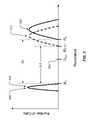
- FIG. 3is an example distribution of the resistance for a number of memory cells of the reference array and memory array, including partial reset for the reference array.
- FIG. 4illustrates an embodiment of sense circuitry for the integrated circuit which can be used to determine if the data set in the reference array is different from the expected data set, and if so to generate a refresh command signal which initiates the refresh operation process.
- FIG. 5is a embodiment of a process which can be executed by the controller using the circuitry of FIG. 4 to determine when to perform a refresh operation.
- FIG. 6is an example top view layout showing the relative sizes and locations of the reference array and memory array.
- FIG. 7illustrates a schematic diagram of an embodiment of a portion of respective memory cells in the memory array and the reference array.
- FIGS. 8A-8Eshow representative prior art memory cell configurations which may be implemented in the memory cells of the memory array and reference array.
- FIGS. 1 to 8 A- 8 EA detailed description of embodiments of the present invention is provided with reference to FIGS. 1 to 8 A- 8 E.
- FIG. 1is an example distribution of the resistance for a number of memory cells each comprising a phase change memory element having one of two states (storing a single bit of data).
- the phase change memory elements of the memory cellsare programmable to a high resistance reset (erased) state 102 and a lower resistance set (programmed) state 100 (storing a single bit of data), each corresponding to a non-overlapping resistance range.
- the change from the high resistance state 102 to the lower resistance state 100is generally a lower current operation in which current heats the phase change material above a transition temperature to cause transition from the amorphous to the crystalline phase.
- the change from the lower resistance state 100 to the higher resistance state 102is generally a higher current operation, which includes a short high current density pulse to melt or breakdown the crystalline structure, after which the phase change material cools quickly, quenching the phase change process and allowing at least a portion of the phase change material to stabilize in the amorphous phase.
- the difference between the highest resistance R 1 of the lower resistance state 100 and the lower resistance R 2 of the high resistance reset state 102defines a read margin 101 used to distinguish cells in the lower resistance state 100 from those in the high resistance state 102 .
- the data stored in a memory cellcan be determined by determining whether the memory cell has a resistance corresponding to the lower resistance state 100 or to the high resistance state 102 , for example by measuring whether the resistance of the memory cell is above or below a threshold resistance value R SA 103 within the read margin 101 .
- phase change memory cells in the reset state 102can experience an erratic “tailing bit” effect in which the resistance of the memory cell decreases over time to below the threshold resistance value R SA 103 , resulting in data retention problems and bit errors for those memory cells.
- the rate of reduction in resistancedepends upon a number of factors, including variations in structure across the array, manufacturing defects in the cells and environmental conditions to which the device is exposed.
- phase change based memory circuitsmust operate at high set and reset operational speeds and use less operational current. These high set and reset speeds and low operational current reduce the difference in resistance between the states 100 and 102 , which further increases the possibility of data retention problems and bit errors.
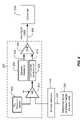
- FIG. 2is a block diagram of a first embodiment of an integrated circuit 210 including a memory array 212 of phase change memory cells and a reference array 250 of phase change memory cells.
- the memory cells of the arrays 212 , 250include an access device such as a diode or transistor, and a phase change memory element.
- the integrated circuit 210includes a controller 234 which controls the application of bias circuitry voltage & current sources 236 to establish low and high resistance states in the memory cells of the memory array 212 and in the memory cells of the reference array 250 .
- the high resistance state for the reference array 250is a “partial reset” state having a minimum resistance less than that of the high resistance state for the memory array 212 .
- bit errors in the reference array 250can be used as an early predictor of bit errors in the memory array 212 and the need to perform a refresh operation.
- a refresh operation of the memory cells of the memory array 212is performed upon determination of a difference between a current data set stored in the reference array 250 and an expected data set.
- the reference array 250has a small number of memory cells compared to that of the memory array 212 , and thus can be read much more quickly and easily.
- the reference array 212may have 100 or more memory cells, while the memory array 212 may have millions or billions of memory cells.
- the detection of bit errors in the data in the reference array 250can be carried out much more quickly than attempting to detect bit errors directly in the memory array 212 .
- the complexity of control and sensing circuitry needed to detect the bit errorsis greatly simplified.
- the memory cells in the reference array 250provides a more relevant statistical predictor of possible bit errors in the memory array 212 than can be achieved using a single reference cell.
- a word line decoder 214is coupled to and in electrical communication with a plurality of word lines 216 arranged along rows in the memory array 212 and reference array 250 .
- a bit line (column) decoderis in electrical communication with a plurality of bit lines 220 arranged along columns in the memory array 212 and reference array 250 . Addresses are supplied on bus 222 to word line decoder and drivers 214 and bit line decoder 218 .
- Sense circuitry and data-in structures in block 224including sense amplifier circuitry for the memory array 212 and reference array 250 , are coupled to bit line decoder 218 via data bus 226 .
- Datais supplied via a data-in line 228 from input/output ports on integrated circuit, to data-in structures in block 224 .
- Other circuitry 230may be included on integrated circuit 210 , such as a general purpose processor or special purpose application circuitry, or a combination of modules providing system-on-a-chip functionality supported by array 212 .
- Datais supplied via a data-out line 232 from the sense amplifiers in block 224 to input/output ports on integrated circuit 210 , or other data destinations internal or external to integrated circuit 210 .
- a controller 234controls the application of bias circuitry voltage & current sources 236 to apply bias arrangements such as read, program, erase, erase verify, program verify, and refresh to the memory cells of the memory array 212 and the reference array 250 .
- the characteristics of the signals sent from the controller 234determine the array 212 , 250 to be accessed as well as the operation to be performed.
- Controller 234may be implemented using special-purpose logic circuitry as known in the art.
- controller 234comprises a general-purpose processor, which may be implemented on the same integrated circuit to execute a computer program to control the operations of the device.
- controller 234implements a refresh mode to refresh the memory cells of the memory array 212 and reference array 250 in response to a refresh command from the reference array sense circuitry of block 224 , the refresh command indicating a difference between a current data set stored in the reference array and an expected data set.
- the memory array 212 and reference array 250can be arranged in different units of the same array to share bit lines and/or word lines, for example different banks, blocks, or sections of the same array.
- the memory array 212 and the reference arraycan be implemented in physically separate arrays.
- each of the memory cells in the arrays 212 , 250store data represented by the resistance of the corresponding memory element.
- the data valuemay be determined, for example, by comparison of voltage or current on a bit line for a selected memory cell to that of a suitable reference current or voltage by sense amplifiers in sense circuitry 224 .
- Reading or writing to a memory cell of arrays 212 , 250can be achieved by applying bias arrangements to provide appropriate voltages and/or current pulses to word lines and bit lines so that current flows through the selected memory cell.
- the level and duration of the pulses appliedis dependent upon the array 212 , 250 , and also the operation to be performed.
- the level and durations of the pulses appliedcan be determined empirically for each embodiment. The various modes of operation for the memory array 212 and reference array 250 are explained in more detail below.
- word line decoder 214facilitates providing a word line with a suitable voltage pulse to turn on the access transistor of the memory cell.
- Bit line decoder 218facilitates supplying a voltage pulse to a bit line of suitable amplitude and duration to induce a current to flow through the memory element, the current raising the temperature of the active region of the memory element above the transition temperature of the phase change material and also above the melting temperature to place the active region in a liquid state.
- the currentis then terminated, for example by terminating the voltages on the bit line and word line, resulting in a relatively quick quenching time as the active region cools, thereby setting the phase change material to a resistance within a resistive value associated with the memory array higher resistance reset state 302 as shown in FIG. 3 .
- word line decoder 214facilitates providing a word line with a suitable voltage pulse to turn on the access transistor of the memory cell.
- Bit line decoder 224facilitates supplying a voltage pulse to a bit line of suitable amplitude and duration to induce a current to flow through the memory element, the current sufficient to raise the temperature of the active region above the transition temperature and cause a transition of at least a portion of the active region from the amorphous phase into the crystalline phase, this transition lowering the resistance of the memory element and setting the resistance of the phase change material within a resistive value range associated with the memory array lower resistance set state 300 .
- the difference between the highest resistance R 1 of the memory array lower resistance set state 300 and the lower resistance R 2 of the memory array higher resistance reset state 302defines a memory array read margin 301 used to distinguish cells of the memory array 212 in the lower resistance set state 300 from those in the higher resistance reset state 302 .
- word line decoder 214facilitates providing a word line with a suitable voltage pulse to turn on the access transistor of the memory cell.
- Bit line decoder 218facilitates supplying a voltage pulse to a bit line of suitable amplitude and duration to induce a current to flow through the memory element that does not result in the memory element undergoing a change in resistive state. The current on the bit line and through the memory cell is dependent upon the resistance of the memory element and thus the data value stored.
- the data value stored in the memory cellmay be determined by detecting whether the resistance of the memory cell corresponds to the high resistance state 302 or low resistance state 300 , for example by comparison of a voltage or current on the corresponding bit line with a suitable voltage or current corresponding to R SA by sense amplifiers of sense circuitry 212 .
- control circuitry in controller 234executes a procedure described in more detail below.
- the reference array 250stores a predetermined data set consisting of the memory cells of the array 250 written to high and low resistance states 312 and 310 .
- the distribution 312 for the “partial reset” state 312 for the reference array 250has a minimum resistance R 2REF less than the minimum resistance R 2 of the distribution 302 for the reset, high resistance state for the memory array 212 .
- the write mode to store the predetermined data set in the reference array 250includes set and partial reset operations for the phase change memory cells.
- the predetermined data set stored in the reference array 250 in the illustrated embodimentis a checkerboard pattern of alternating high and low resistance states between adjacent memory cells in the reference array 250 .
- other techniquescan be used for the arrangement of high and low resistance states for the memory cells in the reference array 250 for the data set.
- word line decoder 214facilitates providing a word line with a suitable voltage pulse to turn on the access transistor of the memory cell.
- Bit line decoder 218facilitates supplying a voltage pulse to a bit line of suitable amplitude and duration to induce a current to flow through the memory element, the current raising the temperature of the active region of the memory element above the transition temperature of the phase change material and also above the melting temperature to place the active region in a liquid state.
- the currentis then terminated, for example by terminating the voltages on the bit line and word line, resulting in a relatively quick quenching time as the active region cools, thereby setting the phase change material to a resistance within a resistive value associated with the reference array higher resistance partial reset state 312 as shown in FIG. 3 .
- Resistances in the distribution 312 for the partial reset state for the memory cells in the reference array 250are achieved by causing the active region of the phase change memory elements of the memory cells of the reference array 250 to have a different mixture of crystalline and amorphous phase material, and/or a smaller active region size, than the phase change memory elements of the memory cells of the memory array 212 in the reset state.
- a first reset pulse adapted to achieve the full reset state represented by the distribution 302may be applied
- a second reset pulse adapted to achieve the partial reset state as represented by distribution 312may be applied, the first and second reset pulses having different values for at least one of pulse width, pulse height and shape of the trailing edge of the pulse.
- the second reset pulsemay have for example a smaller pulse width and/or a longer pulse tail to provide slower quenching time than that of the first reset pulse.
- the reset pulses having the same pulse shapesmay be applied to both the memory array 212 and reference array 250 , and the different distributions 302 and 312 for the reset and partial reset states may be achieved by differences in the cell structures of the arrays 212 , 250 , such as providing features in the cells to obtain different amounts of current density and thus resulting in differences in resistance.
- word line decoder 214facilitates providing a word line with a suitable voltage pulse to turn on the access transistor of the memory cell.
- Bit line decoder 224facilitates supplying a voltage pulse to a bit line of suitable amplitude and duration to induce a current to flow through the memory element, the current sufficient to raise the temperature of the active region above the transition temperature and cause a transition of at least a portion of the active region from the amorphous phase into the crystalline phase, this transition lowering the resistance of the memory element and setting the resistance of the phase change material within a resistive value range associated with the reference array lower resistance set state 310 .
- the reference array lower resistance set state 310 and the memory array lower resistance set state 300correspond tot he same resistive value range.
- the states 300 and 310may correspond to different resistive value ranges.
- the difference between the highest resistance R 1 of the reference array lower resistance set state 310 and the lower resistance R 2REF of the reference array higher resistance reset state 312defines a reference array read margin 315 used to distinguish cells of the reference array 250 in the lower resistance set state 310 from those in the higher resistance partial reset state 312 .
- a read mode of the reference array 250the resistance state of the memory cells are read, and bit errors due to changes in the resistance over time are used to determine when to perform a refresh operation on the memory array 212 .
- word line decoder 214facilitates providing a word line with a suitable voltage pulse to turn on the access transistor of the memory cell.
- Bit line decoder 218facilitates supplying a voltage pulse to a bit line of suitable amplitude and duration to induce a current to flow through the memory element that does not result in the memory element undergoing a change in resistive state. The current on the bit line and through the memory cell is dependent upon the resistance of the memory element and thus the data value stored.
- the data value stored in the memory cellmay be determined by detecting whether the resistance of the memory cell corresponds to the high resistance state 302 or low resistance state 300 , for example by comparison of a voltage or current on the corresponding bit line with a suitable voltage or current corresponding to R SA by sense amplifiers of sense circuitry 212 .
- FIG. 4illustrates an embodiment of sense circuitry 224 for the integrated circuit 210 , which can be used to determine if the data set in the reference array 250 is different from the expected predetermined data set, and if so to generate a refresh command signal to the controller 234 which initiates the refresh operation process of the memory array 212 and reference array 250 .
- the reference array 250is coupled by bit lines 220 through bit line decoder 218 to an input of sense amplifier 410 .
- An R SA reference source 420is coupled to the other input of the sense amplifier 410
- a sense enable signal SENis coupled to the sense amplifier 410 .
- the sense amplifier 410is responsive to the difference at its inputs to generate an output signal indicating the resistive state of the memory element and thus indicating the data value stored in the memory cell.
- the output signal of the sense amplifier 410is provided to checksum generator 430 .
- the checksum generator 430computes a checksum 435 using the data values of the data set read from the memory cells of the reference array 250 , and supplies the computed checksum 435 to comparator 440 .
- the checksum generator 430may be implemented using special-purpose logic circuitry as known in the art.
- the checksum generator 430comprises a general-purpose processor, which may be implemented on the same integrated circuit to execute a computer program to control the operations of the device.
- a combination of special-purpose logic circuitry and a general-purpose processormay be utilized for implementation of the checksum generator 430
- the circuitry 224also includes a register 400 storing a parameter 405 which represents the predetermined data set for the reference array, and provides this parameter 405 to the comparator 440 as part of the process described below.
- the parameter 405is the expected checksum 405 which corresponds to the predetermined data set.
- the comparator 440compares the computed checksum 435 and the expected checksum 405 , and generates a refresh command signal REFRESH CMD 450 if the computed checksum 435 and the expected checksum are different 405 .
- the controller 234is responsive to the refresh command signal REFRESH CMD 450 to then perform a refresh operation of the memory array 212 and the reference array 250 .
- FIG. 5is an embodiment of a process 500 which can be executed by the controller 234 using the circuitry 234 of FIG. 4 to determine when to perform a refresh operation of the memory array 212 and the reference array 250 .
- the process 500is executed upon receiving a refresh check command. Until the refresh check command is received, the process loops in blocks 510 and 520 .
- the controller 234Upon receiving the refresh check command (block 520 ), the controller 234 causes a read process of the data set stored in the reference array 250 using the sense amplifiers of block 410 , and causes the computation of the checksum 435 from the stored data set by the checksum generator 430 of the sense circuitry 224 (block 530 ).
- the computed checksum 435 and the expected checksum 405 stored in the register 400are compared by comparator 440 (block 540 ). If the expected checksum 405 and the computed checksum 435 match at block 540 , then the data stored in reference array 250 is determined to correspond to the predetermined data set and a refresh operation is not required. The process 500 loops back to block 510 to await another refresh check command.
- the controller 234is responsive to the REFRESH CMD 450 to cause a refresh operation to be performed on the memory array 212 and the reference array 250 .
- the controller 234causes the application of appropriate read bias arrangements to read the resistance of the memory cells, and if necessary causes the application of appropriate bias arrangements to refresh the resistance of the corresponding memory elements to offset any change in resistance that may have occurred between refresh cycles.
- bit errors in the reference array 250may also be used. For example, in embodiments in which the reference array 250 stores a checkerboard pattern, bit errors may be determined by detecting consecutive memory cells having the same resistance state using logic circuitry.
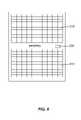
- FIG. 6is an example top view layout showing the relative sizes and locations of the reference array 250 and memory array 212 .
- the relative sizes and locations of the arrays 250 , 212may be different.
- FIG. 7illustrates a schematic diagram of an embodiment of a portion of respective memory cells of the memory array 212 and the reference array 250 .
- the memory array 212 and the reference array 250share the bit lines 220 .
- other configurationsmay be used, such as sharing the word lines 216 .
- the memory array 212includes memory cells 701 , 702 , 703 , 704 having respective memory elements 711 , 712 , 713 , 714 .
- the reference array 250includes memory cells 721 , 722 , 723 , 724 having respective memory elements 721 , 722 , 723 , 724 .
- the arrays 212 , 250include a plurality of word lines 216 including word lines 216 a , 216 b , 216 c , 216 d extending in parallel in a first direction, and a plurality of bit lines 220 including bit lines 220 a , 220 b extending in parallel in a second direction perpendicular to the first direction.
- Sources of each of the four access transistors illustrated in the memory array 212are connected in common to source line 796 a that terminates in a source line termination circuit 795 , such as a ground terminal.
- source line termination circuit 795such as a ground terminal.
- the sources of the access devicesare not electrically connects, but independently controllable.
- Sources of each of the four access transistors illustrated in the reference array 250are connected in common to source line 796 b that terminates in a source line termination circuit 795 .
- the source line termination circuit 795may include bias circuits such as voltage and current sources, and decoding circuits for applying bias arrangements other than ground to the source lines 796 in some embodiments.
- Reading or writing to the memory cells of the arrays 212 , 250can be achieved by applying appropriate bias arrangements discussed above.
- the memory cells of the arrays 212 , 250are distinguished by their address to determine the characteristics of the signals sent by the controller 234 to couple the bias circuitry to apply pulses to operate the memory cells of the arrays 212 , 250 .
- the active regions of the phase change memory elements of the memory cells of the reference array 250have a different mixture of crystalline and amorphous phase material, or a smaller active region, than phase change memory elements of the memory cells of the memory array 212 in the reset state 302 .
- a first reset pulsemay be applied, and in a reset operation of a memory cell in the reference array 250 a second reset pulse may be applied, the first and second reset pulses having different values for at least one of pulse width, pulse height, and shape of the trailing edge of the pulse.
- reset pulses having the same pulse shapesmay be applied to both the memory array 212 and reference array 250 , and the different distributions 302 and 312 for the reset and set states may be achieved by differences in the cell structures of the arrays 212 , 250 , such as providing features in the cells to obtain different amounts of current density and thus resulting in differences in resistance.
- the predetermined data set stored in the reference array 250 in the illustrated embodimentis a checkerboard pattern of alternating high and low resistance states between adjacent memory cells in the reference array 250 .
- the memory elements 731 , 734are programmed to the set state 310
- the memory elements 732 , 733are programmed to the partial reset state 312 .
- memory array 212 and reference array 250are not limited to the array configuration illustrated in FIG. 7 , and other array configurations can also be used including implementing different configurations for each of the arrays 212 and 250 .
- the memory array 212 and reference array 250include field effect transistor access devices.
- other access devicessuch as diodes or bipolar junction transistors may be used, including using different types of access devices for the two arrays 212 , 250 .
- the reference array 250 and the memory array 212are arranged at different locations within a single memory array to share common control circuitry and bias circuitry.
- the reference array 250 and the memory array 212may be arranged in separate arrays, and may also each have separate control circuitry and bias circuitry.
- the memory cells of the reference array 250 and the memory cells of the memory array 212have memory elements with the same physical configuration.
- the memory cells of the arrays 250 , 212may comprise various types of memory elements having different physical configurations.
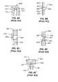
- FIGS. 8A-8Eshow representative prior art memory cell structures which may be implemented in the memory cells of the arrays 250 , 212 .
- FIG. 8Ais a simplified cross-sectional view illustrating a first configuration for memory element 820 coupled to first and second electrodes 812 , 814 .
- the first electrode 812may, for example, be coupled to a terminal of an access device such as a diode or transistor, while the second electrode 814 may be coupled to a bit line.
- a dielectric spacer 813 having a width 815separates the first and second electrodes 812 , 814 .
- the phase change material of memory element 920extends across the dielectric spacer 813 and contacts the first and second electrodes 812 , 814 , thereby defining an inter-electrode path between the first and second electrodes 812 , 814 having a path length defined by the width 815 of the dielectric spacer 813 .
- the active region 818 of the phase change material of the memory element 920heats up more quickly than the remainder of the memory element 920 .
- FIG. 8Bis a simplified cross-sectional view illustrating a second configuration for memory element 920 coupled to first and second electrodes 822 , 824 .
- the phase change material of the memory element 920has an active region 828 and contacts the first and second electrodes 822 , 824 at top and bottom surfaces 823 , 829 respectively.
- the memory element 920has a width 821 the same as that of the first and second electrodes 822 , 824 .
- FIG. 8Cis a simplified cross-sectional view illustrating a third configuration for memory element 920 coupled to first and second electrodes 832 , 834 , the phase change material of memory element 920 having an active region 838 .
- the first and second electrodes 832 , 834are separated by dielectric spacer 835 .
- the first and second electrodes 832 , 834 and the dielectric spacer 835have a sidewall surface 831 .
- the phase change material of memory element 920is on the sidewall surface 831 and extends across the dielectric spacer 835 to contact the first and second electrodes 832 , 834 .
- FIG. 8Dis a simplified cross-sectional view illustrating a fourth configuration for memory element 920 coupled to first and second electrodes 842 , 844 .
- the phase change material of memory element 920has an active region 848 and contacts the first and second electrodes 842 , 844 at top and bottom surfaces 843 , 849 respectively.
- the memory element 920has a width 841 less than that of the first and second electrodes 842 , 844 .
- FIG. 8Eis a simplified cross-sectional view illustrating a fifth configuration for memory element 920 coupled to first and second electrodes 854 , 852 .
- the first electrode 854has a width 851 less than width 853 of the second electrode 852 and memory element 920 . Because of the difference between width 851 and width 853 , in operation the current density in the phase change material of memory element 920 is largest in the region adjacent the first electrode 854 , resulting in the active region 858 having a “mushroom” shape as shown in the Figure.
- Embodiments of the memory cells described hereininclude phase change based memory materials, including chalcogenide based materials and other materials, for the programmable resistance memory elements.
- Chalcogensinclude any of the four elements oxygen (O), sulfur (S), selenium (Se), and tellurium (Te), forming part of group VIA of the periodic table.
- Chalcogenidescomprise compounds of a chalcogen with a more electropositive element or radical.
- Chalcogenide alloyscomprise combinations of chalcogenides with other materials such as transition metals.
- a chalcogenide alloyusually contains one or more elements from group IVA of the periodic table of elements, such as germanium (Ge) and tin (Sn).
- chalcogenide alloysinclude combinations including one or more of antimony (Sb), gallium (Ga), indium (In), and silver (Ag).
- Sbantimony
- Gagallium
- Inindium
- silversilver
- phase change based memory materialsinclude alloys of: Ga/Sb, In/Sb, In/Se, Sb/Te, Ge/Te, Ge/Sb/Te, In/Sb/Te, Ga/Se/Te, Sn/Sb/Te, In/Sb/Ge, Ag/In/Sb/Te, Ge/Sn/Sb/Te, Ge/Sb/Se/Te and Te/Ge/Sb/S.
- compositionscan be workable.
- the compositionscan be characterized as Te a Ge b Sb 100-(a+b) .
- One researcherhas described the most useful alloys as having an average concentration of Te in the deposited materials well below 70%, typically below about 60% and ranged in general from as low as about 23% up to about 58% Te and most preferably about 48% to 58% Te.
- Concentrations of Gewere above about 5% and ranged from a low of about 8% to about 30% average in the material, remaining generally below 50 %. Most preferably, concentrations of Ge ranged from about 8% to about 40%. The remainder of the principal constituent elements in this composition was Sb.
- a transition metalsuch as chromium (Cr), iron (Fe), nickel (Ni), niobium (Nb), palladium (Pd), platinum (Pt) and mixtures or alloys thereof may be combined with Ge/Sb/Te to form a phase change alloy that has programmable resistive properties.
- chromium (Cr)iron (Fe), nickel (Ni), niobium (Nb), palladium (Pd), platinum (Pt) and mixtures or alloys thereof
- Ge/Sb/Techromium
- Specific examples of memory materials that may be usefulare given in Ovshinsky '112 at columns 11-13, which examples are hereby incorporated by reference.
- Chalcogenides and other phase change materialsare doped with impurities in some embodiments to modify conductivity, transition temperature, melting temperature, and other properties of memory elements using the doped chalcogenides.
- Representative impurities used for doping chalcogenidesinclude nitrogen, silicon, oxygen, silicon dioxide, silicon nitride, copper, silver, gold, aluminum, aluminum oxide, tantalum, tantalum oxide, tantalum nitride, titanium and titanium oxide. See, e.g., U.S. Pat. No. 6,800,504, and U.S. Patent Application Publication No. U.S. 2005/0029502.
- Phase change alloysare capable of being switched between a first structural state in which the material is in a generally amorphous solid phase, and a second structural state in which the material is in a generally crystalline solid phase in its local order in the active channel region of the cell. These alloys are at least bistable.
- amorphousis used to refer to a relatively less ordered structure, more disordered than a single crystal, which has the detectable characteristics such as higher electrical resistivity than the crystalline phase.
- crystallineis used to refer to a relatively more ordered structure, more ordered than in an amorphous structure, which has detectable characteristics such as lower electrical resistivity than the amorphous phase.
- phase change materialsmay be electrically switched between different detectable states of local order across the spectrum between completely amorphous and completely crystalline states.
- Other material characteristics affected by the change between amorphous and crystalline phasesinclude atomic order, free electron density and activation energy.
- the materialmay be switched either into different solid phases or into mixtures of two or more solid phases, providing a gray scale between completely amorphous and completely crystalline states.
- the electrical properties in the materialmay vary accordingly.
- Phase change alloyscan be changed from one phase state to another by application of electrical pulses. It has been observed that a shorter, higher amplitude pulse tends to change the phase change material to a generally amorphous state. A longer, lower amplitude pulse tends to change the phase change material to a generally crystalline state. The energy in a shorter, higher amplitude pulse is high enough to allow for bonds of the crystalline structure to be broken and short enough to prevent the atoms from realigning into a crystalline state. Appropriate profiles for pulses can be determined, without undue experimentation, specifically adapted to a particular phase change alloy. In following sections of the disclosure, the phase change material is referred to as GST, and it will be understood that other types of phase change materials can be used. A material useful for implementation of a PCRAM described herein is Ge 2 Sb 2 Te 5 .
- RRAMresistance random access memory
- metal-oxidesincluding tungsten-oxide (WO x ), NiO, Nb 2 O 5 , CuO 2 , Ta 2 O 5 , Al 2 O 3 , CoO, Fe 2 O 3 , HfO 2 , TiO 2 , SrTiO 3 , (BaSr)TiO 3 .
- MRAMmagnetoresistance random access memory
- STTspin-torque-transfer
- Additional examplesinclude solid electrolyte materials used for programmable-metallization-cell (PMC) memory, or nano-ionic memory, such as silver-doped germanium sulfide electrolytes and copper-doped germanium sulfide electrolytes.
- PMCprogrammable-metallization-cell
- nano-ionic memorysuch as silver-doped germanium sulfide electrolytes and copper-doped germanium sulfide electrolytes.
- An exemplary method for forming chalcogenide materialuses PVD-sputtering or magnetron-sputtering method with source gas(es) of Ar, N2, and/or He, etc. at the pressure of 1 mTorr ⁇ 100 mTorr.
- the depositionis usually done at room temperature.
- a collimator with an aspect ratio of 1 ⁇ 15can be used to improve the fill-in performance.
- a DC bias of several tens of volts to several hundreds of voltsis also used.
- the combination of DC bias and the collimatercan be used simultaneously.
- a post-deposition annealing treatment in a vacuum or in an N2 ambientis optionally performed to improve the crystallize state of chalcogenide material.
- the annealing temperaturetypically ranges from 100° C. to 400° C. with an anneal time of less than 30 minutes.
Landscapes
- Chemical & Material Sciences (AREA)
- Crystallography & Structural Chemistry (AREA)
- Engineering & Computer Science (AREA)
- Computer Hardware Design (AREA)
- Semiconductor Memories (AREA)
Abstract
Description
- 1. Field of the Invention
- The present invention relates to high density memory devices based on phase change based memory materials, including chalcogenide based materials and on other programmable resistive materials, and methods for refreshing such devices.
- 2. Description of Related Art
- Phase change based memory materials, like chalcogenide based materials and similar materials, can be caused to change phase between amorphous and crystalline states by application of electrical current at levels suitable for implementation in integrated circuits. The generally amorphous state is characterized by higher electrical resistivity than the generally crystalline state, which can be readily sensed to indicate data. These properties have generated interest in using programmable resistive material to form nonvolatile circuits, which can be read and written with random access.
- The change from the amorphous to the crystalline state, referred to as set herein, is generally a lower current operation. The change from crystalline to amorphous, referred to as reset herein, is generally a higher current operation, which includes a short high current density pulse to melt or breakdown the crystalline structure, after which the phase change material cools quickly, quenching the phase change process and allowing at least a portion of the phase change material to stabilize in the amorphous state.
- It has been observed that some phase change memory cells in the reset state experience a decrease in resistance over time to below a threshold value used to distinguish between the reset and set states, resulting in data retention problems and bit errors for those memory cells. For example, a memory cell in which the active region has been reset to a generally amorphous state may over time develop a distribution of crystalline regions in the active region. If these crystalline regions connect to form a low resistance path through the active region, when the memory cell is read a lower resistance state will be detected and result in a data error. See, Gleixner, “Phase Change Memory Reliability”, 22nd NVSMW, 2007.
- One attempt at addressing the data retention problems caused by the decrease in resistance over time is to maintain a relatively large read margin between the set and reset states. However, a relatively large read margin typically requires a slow set operation and a high reset current in order to obtain the large difference in resistance between the set and reset states. The relatively slow set operation and high reset current limit the operational speed of the device, restricting the use of phase change based memory circuits as high speed memory.
- Thus, integrated circuits employing phase change based memory circuits typically also include other types of memory circuits in order to fulfill the memory performance requirements for the various functions of the integrated circuit. These different types of memory circuits are embedded at various locations in the integrated circuit, and typically include SRAM and DRAM memory circuits in order to provide high access speed memory for the integrated circuit. However, integration of different types of memory circuits for the various memory applications in an integrated circuit can be difficult and result in highly complex designs.
- It has also been proposed to address the data retention problems by periodically refreshing phase change memory cells to offset any change in resistance that may occur over time.
- One approach is to periodically read the resistance of each memory cell in the array to determine when to selectively perform a refresh operation on that particular memory cell. See, U.S. Patent Application Publication No. US 2008/0117704 entitled “Resistive Memory Including Selective Refresh Operation” by Happ et al, and U.S. Pat. No. 6,768,665 entitled “Refreshing Memory Cells of a Phase Change Material Memory Device” by Parkinson et al.
- Another approach is to perform a refresh operation when the phase change memory has been accessed a number of times larger than a predetermined number. See, U.S. Patent Application Publication No. US 2008/0170431 entitled “Driving Method and System for a Phase Change Memory” by Sheu et al.
- Another approach is to apply stress to a dummy set of memory cells based on the number of read and write operations performed on a main array of memory cells, and detecting changes in the resistance of the dummy set to determine when to refresh the main array of memory cells. See, U.S. Patent Application No. 2006/0158948 entitled “Memory Device” by Fuji.
- It is therefore desirable to provide phase change based memory devices and methods for operating such devices which address the data retention issues discussed above and result in improved data storage performance.
- A memory device as described herein includes a reference array of phase change memory cells and a memory array of phase change memory cells, where a difference between a current data set stored in the reference array and an expected data set is used to determine when to refresh the memory array.
- The memory device includes bias circuitry to establish low and high resistance states in the memory array and in the reference array. The high resistance state for the reference array is a “partial reset” state having a minimum resistance less than a minimum resistance of the high resistance state for the memory array.
- The device further includes sense circuitry to read the reference array and to generate a refresh command signal if there is a difference between a current data set stored in the reference array and an expected data set, and control circuitry responsive to the refresh command signal to perform a refresh operation on the memory array.
- As a result of the lower minimum resistance for the partial reset state for the reference array, the data retention performance of the reference array is worse than that of the memory array and is used as an early predictor of bit errors in the memory array and the need to perform refresh operation.
- The reference array has a small number of memory cells compared to that of the memory array. In one example, the reference array may have on the order of 100 memory cells, while the memory array may have millions or billions of memory cells.
- As a result of the relatively small number of memory cells in the reference array, the detection of bit errors in the data in the reference array can be carried out much more quickly than detecting bit errors directly in the memory array. Additionally, the complexity of control and sensing circuitry needed to detect the bit errors is greatly simplified.
- Since the probability of a bit error occurring in any particular memory cell is preferably small, the reference array also provides a more relevant statistical predictor of possible bit errors in the memory array than can be achieved using a single reference cell.
- Methods for operating memory devices comprising a memory array of phase change cells and a reference array of phase change cells are also disclosed herein.
- Other aspects and advantages of the present invention can be seen on review of the drawings, the detailed description, and the claims which follow.
FIG. 1 is an example distribution of the resistance for a number of memory cells each comprising a phase change memory element having one of two states.FIG. 2 is a block diagram of a first embodiment of an integrated circuit including a memory array of phase change memory cells and a reference array of phase change memory cells as described herein.FIG. 3 is an example distribution of the resistance for a number of memory cells of the reference array and memory array, including partial reset for the reference array.FIG. 4 illustrates an embodiment of sense circuitry for the integrated circuit which can be used to determine if the data set in the reference array is different from the expected data set, and if so to generate a refresh command signal which initiates the refresh operation process.FIG. 5 is a embodiment of a process which can be executed by the controller using the circuitry ofFIG. 4 to determine when to perform a refresh operation.FIG. 6 is an example top view layout showing the relative sizes and locations of the reference array and memory array.FIG. 7 illustrates a schematic diagram of an embodiment of a portion of respective memory cells in the memory array and the reference array.FIGS. 8A-8E show representative prior art memory cell configurations which may be implemented in the memory cells of the memory array and reference array.- A detailed description of embodiments of the present invention is provided with reference to FIGS.1 to8A-8E.
- In phase change memory, data is stored by causing transitions in an active region of the phase change material between amorphous and crystalline phases.
FIG. 1 is an example distribution of the resistance for a number of memory cells each comprising a phase change memory element having one of two states (storing a single bit of data). The phase change memory elements of the memory cells are programmable to a high resistance reset (erased)state 102 and a lower resistance set (programmed) state100 (storing a single bit of data), each corresponding to a non-overlapping resistance range. - The change from the
high resistance state 102 to thelower resistance state 100 is generally a lower current operation in which current heats the phase change material above a transition temperature to cause transition from the amorphous to the crystalline phase. The change from thelower resistance state 100 to thehigher resistance state 102 is generally a higher current operation, which includes a short high current density pulse to melt or breakdown the crystalline structure, after which the phase change material cools quickly, quenching the phase change process and allowing at least a portion of the phase change material to stabilize in the amorphous phase. - The difference between the highest resistance R1 of the
lower resistance state 100 and the lower resistance R2 of the highresistance reset state 102 defines aread margin 101 used to distinguish cells in thelower resistance state 100 from those in thehigh resistance state 102. The data stored in a memory cell can be determined by determining whether the memory cell has a resistance corresponding to thelower resistance state 100 or to thehigh resistance state 102, for example by measuring whether the resistance of the memory cell is above or below a thresholdresistance value R SA103 within theread margin 101. - In order to reliably distinguish between the
reset state 102 and theset state 100, it is important to maintain a relativelylarge read margin 101. However, it has been observed that some phase change memory cells in thereset state 102 can experience an erratic “tailing bit” effect in which the resistance of the memory cell decreases over time to below the thresholdresistance value R SA103, resulting in data retention problems and bit errors for those memory cells. The rate of reduction in resistance depends upon a number of factors, including variations in structure across the array, manufacturing defects in the cells and environmental conditions to which the device is exposed. - Furthermore, in order to meet high speed memory requirements such as those typically required of DRAM and SRAM, phase change based memory circuits must operate at high set and reset operational speeds and use less operational current. These high set and reset speeds and low operational current reduce the difference in resistance between the
states FIG. 2 is a block diagram of a first embodiment of anintegrated circuit 210 including amemory array 212 of phase change memory cells and areference array 250 of phase change memory cells. The memory cells of thearrays - As described in more detail below, the
integrated circuit 210 includes acontroller 234 which controls the application of bias circuitry voltage ¤t sources 236 to establish low and high resistance states in the memory cells of thememory array 212 and in the memory cells of thereference array 250. - The high resistance state for the
reference array 250 is a “partial reset” state having a minimum resistance less than that of the high resistance state for thememory array 212. As a result, over time the data retention performance of thereference array 250 is worse than that of thememory array 212, and bit errors in thereference array 250 can be used as an early predictor of bit errors in thememory array 212 and the need to perform a refresh operation. Thus, upon determination of a difference between a current data set stored in thereference array 250 and an expected data set, a refresh operation of the memory cells of thememory array 212 is performed. - The
reference array 250 has a small number of memory cells compared to that of thememory array 212, and thus can be read much more quickly and easily. In one example, thereference array 212 may have100 or more memory cells, while thememory array 212 may have millions or billions of memory cells. As a result of the relatively small number of memory cells in thereference array 212, the detection of bit errors in the data in thereference array 250 can be carried out much more quickly than attempting to detect bit errors directly in thememory array 212. Additionally, the complexity of control and sensing circuitry needed to detect the bit errors is greatly simplified. - Also, since the probability of a bit error occurring in any particular memory cell is preferably small, the memory cells in the
reference array 250 provides a more relevant statistical predictor of possible bit errors in thememory array 212 than can be achieved using a single reference cell. - A
word line decoder 214 is coupled to and in electrical communication with a plurality ofword lines 216 arranged along rows in thememory array 212 andreference array 250. A bit line (column) decoder is in electrical communication with a plurality ofbit lines 220 arranged along columns in thememory array 212 andreference array 250. Addresses are supplied onbus 222 to word line decoder anddrivers 214 andbit line decoder 218. Sense circuitry and data-in structures inblock 224, including sense amplifier circuitry for thememory array 212 andreference array 250, are coupled tobit line decoder 218 viadata bus 226. Data is supplied via a data-inline 228 from input/output ports on integrated circuit, to data-in structures inblock 224.Other circuitry 230 may be included onintegrated circuit 210, such as a general purpose processor or special purpose application circuitry, or a combination of modules providing system-on-a-chip functionality supported byarray 212. Data is supplied via a data-outline 232 from the sense amplifiers inblock 224 to input/output ports onintegrated circuit 210, or other data destinations internal or external tointegrated circuit 210. - A
controller 234, implemented in this example using a bias arrangement state machine, controls the application of bias circuitry voltage ¤t sources 236 to apply bias arrangements such as read, program, erase, erase verify, program verify, and refresh to the memory cells of thememory array 212 and thereference array 250. The characteristics of the signals sent from thecontroller 234 determine thearray Controller 234 may be implemented using special-purpose logic circuitry as known in the art. In alternative embodiments,controller 234 comprises a general-purpose processor, which may be implemented on the same integrated circuit to execute a computer program to control the operations of the device. In yet other embodiments, a combination of special-purpose logic circuitry and a general-purpose processor may be utilized for implementation ofcontroller 234. As described in more detail below, thecontroller 234 implements a refresh mode to refresh the memory cells of thememory array 212 andreference array 250 in response to a refresh command from the reference array sense circuitry ofblock 224, the refresh command indicating a difference between a current data set stored in the reference array and an expected data set. - The
memory array 212 andreference array 250 can be arranged in different units of the same array to share bit lines and/or word lines, for example different banks, blocks, or sections of the same array. Alternatively, thememory array 212 and the reference array can be implemented in physically separate arrays. - In operation each of the memory cells in the
arrays sense circuitry 224. - Reading or writing to a memory cell of
arrays array memory array 212 andreference array 250 are explained in more detail below. - In biasing arrangements for a reset (erase) operation for a memory cell in the
memory array 212,word line decoder 214 facilitates providing a word line with a suitable voltage pulse to turn on the access transistor of the memory cell.Bit line decoder 218 facilitates supplying a voltage pulse to a bit line of suitable amplitude and duration to induce a current to flow through the memory element, the current raising the temperature of the active region of the memory element above the transition temperature of the phase change material and also above the melting temperature to place the active region in a liquid state. The current is then terminated, for example by terminating the voltages on the bit line and word line, resulting in a relatively quick quenching time as the active region cools, thereby setting the phase change material to a resistance within a resistive value associated with the memory array higher resistance resetstate 302 as shown inFIG. 3 . - In biasing arrangements for a set (program) operation for a memory cell in the
memory array 212,word line decoder 214 facilitates providing a word line with a suitable voltage pulse to turn on the access transistor of the memory cell.Bit line decoder 224 facilitates supplying a voltage pulse to a bit line of suitable amplitude and duration to induce a current to flow through the memory element, the current sufficient to raise the temperature of the active region above the transition temperature and cause a transition of at least a portion of the active region from the amorphous phase into the crystalline phase, this transition lowering the resistance of the memory element and setting the resistance of the phase change material within a resistive value range associated with the memory array lower resistance setstate 300. - The difference between the highest resistance R1of the memory array lower resistance set
state 300 and the lower resistance R2of the memory array higher resistance resetstate 302 defines a memory array readmargin 301 used to distinguish cells of thememory array 212 in the lower resistance setstate 300 from those in the higher resistance resetstate 302. - In a read operation for a memory cell in the
memory array 212,word line decoder 214 facilitates providing a word line with a suitable voltage pulse to turn on the access transistor of the memory cell.Bit line decoder 218 facilitates supplying a voltage pulse to a bit line of suitable amplitude and duration to induce a current to flow through the memory element that does not result in the memory element undergoing a change in resistive state. The current on the bit line and through the memory cell is dependent upon the resistance of the memory element and thus the data value stored. Thus, the data value stored in the memory cell may be determined by detecting whether the resistance of the memory cell corresponds to thehigh resistance state 302 orlow resistance state 300, for example by comparison of a voltage or current on the corresponding bit line with a suitable voltage or current corresponding to RSAby sense amplifiers ofsense circuitry 212. - In a refresh mode of the
memory array 212, the control circuitry incontroller 234 executes a procedure described in more detail below. - The
reference array 250 stores a predetermined data set consisting of the memory cells of thearray 250 written to high and low resistance states312 and310. As can be seen inFIG. 3 , thedistribution 312 for the “partial reset”state 312 for thereference array 250 has a minimum resistance R2REFless than the minimum resistance R2of thedistribution 302 for the reset, high resistance state for thememory array 212. - As discussed below, changes over time in the data set stored in the
reference array 250 caused by bit errors in the memory cells of thereference array 250 are used to determine when to perform a refresh operation on both thememory array 212 andreference array 250. - The write mode to store the predetermined data set in the
reference array 250 includes set and partial reset operations for the phase change memory cells. The predetermined data set stored in thereference array 250 in the illustrated embodiment is a checkerboard pattern of alternating high and low resistance states between adjacent memory cells in thereference array 250. Alternatively, other techniques can be used for the arrangement of high and low resistance states for the memory cells in thereference array 250 for the data set. - In biasing arrangements for a partial reset operation for a memory cell in the
reference array 250,word line decoder 214 facilitates providing a word line with a suitable voltage pulse to turn on the access transistor of the memory cell.Bit line decoder 218 facilitates supplying a voltage pulse to a bit line of suitable amplitude and duration to induce a current to flow through the memory element, the current raising the temperature of the active region of the memory element above the transition temperature of the phase change material and also above the melting temperature to place the active region in a liquid state. The current is then terminated, for example by terminating the voltages on the bit line and word line, resulting in a relatively quick quenching time as the active region cools, thereby setting the phase change material to a resistance within a resistive value associated with the reference array higher resistancepartial reset state 312 as shown inFIG. 3 . - Resistances in the
distribution 312 for the partial reset state for the memory cells in thereference array 250 are achieved by causing the active region of the phase change memory elements of the memory cells of thereference array 250 to have a different mixture of crystalline and amorphous phase material, and/or a smaller active region size, than the phase change memory elements of the memory cells of thememory array 212 in the reset state. - For example, in a reset operation of a memory cell in the memory array212 a first reset pulse adapted to achieve the full reset state represented by the
distribution 302 may be applied, and in a reset operation of a memory cell in the reference array250 a second reset pulse adapted to achieve the partial reset state as represented bydistribution 312 may be applied, the first and second reset pulses having different values for at least one of pulse width, pulse height and shape of the trailing edge of the pulse. To achieve thedifferent distributions - Alternatively, the reset pulses having the same pulse shapes may be applied to both the
memory array 212 andreference array 250, and thedifferent distributions arrays - In biasing arrangements for a set (program) operation for a memory cell in the
reference array 250,word line decoder 214 facilitates providing a word line with a suitable voltage pulse to turn on the access transistor of the memory cell.Bit line decoder 224 facilitates supplying a voltage pulse to a bit line of suitable amplitude and duration to induce a current to flow through the memory element, the current sufficient to raise the temperature of the active region above the transition temperature and cause a transition of at least a portion of the active region from the amorphous phase into the crystalline phase, this transition lowering the resistance of the memory element and setting the resistance of the phase change material within a resistive value range associated with the reference array lower resistance setstate 310. - In the illustrated embodiment the reference array lower resistance set
state 310 and the memory array lower resistance setstate 300 correspond tot he same resistive value range. Alternatively, thestates - The difference between the highest resistance R1of the reference array lower resistance set
state 310 and the lower resistance R2REFof the reference array higher resistance resetstate 312 defines a reference array readmargin 315 used to distinguish cells of thereference array 250 in the lower resistance setstate 310 from those in the higher resistancepartial reset state 312. - In a read mode of the
reference array 250 the resistance state of the memory cells are read, and bit errors due to changes in the resistance over time are used to determine when to perform a refresh operation on thememory array 212. - In a read operation for a memory cell in the
reference array 250,word line decoder 214 facilitates providing a word line with a suitable voltage pulse to turn on the access transistor of the memory cell.Bit line decoder 218 facilitates supplying a voltage pulse to a bit line of suitable amplitude and duration to induce a current to flow through the memory element that does not result in the memory element undergoing a change in resistive state. The current on the bit line and through the memory cell is dependent upon the resistance of the memory element and thus the data value stored. Thus, the data value stored in the memory cell may be determined by detecting whether the resistance of the memory cell corresponds to thehigh resistance state 302 orlow resistance state 300, for example by comparison of a voltage or current on the corresponding bit line with a suitable voltage or current corresponding to RSAby sense amplifiers ofsense circuitry 212. FIG. 4 illustrates an embodiment ofsense circuitry 224 for theintegrated circuit 210, which can be used to determine if the data set in thereference array 250 is different from the expected predetermined data set, and if so to generate a refresh command signal to thecontroller 234 which initiates the refresh operation process of thememory array 212 andreference array 250.- In
FIG. 4 thereference array 250 is coupled bybit lines 220 throughbit line decoder 218 to an input ofsense amplifier 410. An RSAreference source420 is coupled to the other input of thesense amplifier 410, and a sense enable signal SEN is coupled to thesense amplifier 410. During a read operation of a memory cell of thereference array 250, thesense amplifier 410 is responsive to the difference at its inputs to generate an output signal indicating the resistive state of the memory element and thus indicating the data value stored in the memory cell. The output signal of thesense amplifier 410 is provided tochecksum generator 430. - During the read process of the
reference array 250, thechecksum generator 430 computes achecksum 435 using the data values of the data set read from the memory cells of thereference array 250, and supplies the computedchecksum 435 to comparator440. - The
checksum generator 430 may be implemented using special-purpose logic circuitry as known in the art. In alternative embodiments, thechecksum generator 430 comprises a general-purpose processor, which may be implemented on the same integrated circuit to execute a computer program to control the operations of the device. In yet other embodiments, a combination of special-purpose logic circuitry and a general-purpose processor may be utilized for implementation of thechecksum generator 430 - The
circuitry 224 also includes aregister 400 storing aparameter 405 which represents the predetermined data set for the reference array, and provides thisparameter 405 to the comparator440 as part of the process described below. In the illustrated embodiment theparameter 405 is the expectedchecksum 405 which corresponds to the predetermined data set. - The comparator440 compares the computed
checksum 435 and the expectedchecksum 405, and generates a refresh commandsignal REFRESH CMD 450 if the computedchecksum 435 and the expected checksum are different405. Thecontroller 234 is responsive to the refresh commandsignal REFRESH CMD 450 to then perform a refresh operation of thememory array 212 and thereference array 250. FIG. 5 is an embodiment of aprocess 500 which can be executed by thecontroller 234 using thecircuitry 234 ofFIG. 4 to determine when to perform a refresh operation of thememory array 212 and thereference array 250.- In
FIG. 5 , theprocess 500 is executed upon receiving a refresh check command. Until the refresh check command is received, the process loops inblocks - Upon receiving the refresh check command (block520), the
controller 234 causes a read process of the data set stored in thereference array 250 using the sense amplifiers ofblock 410, and causes the computation of thechecksum 435 from the stored data set by thechecksum generator 430 of the sense circuitry224 (block530). - Next, the computed
checksum 435 and the expectedchecksum 405 stored in theregister 400 are compared by comparator440 (block540). If the expectedchecksum 405 and the computedchecksum 435 match atblock 540, then the data stored inreference array 250 is determined to correspond to the predetermined data set and a refresh operation is not required. Theprocess 500 loops back to block510 to await another refresh check command. - It the expected
checksum 405 and the computedchecksum 435 do not match atblock 540, then thereference array 250 has bit errors and the comparator440 generates the refresh commandsignal REFRESH CMD 450. Theprocess 500 the continues to block550. - At
block 550, thecontroller 234 is responsive to theREFRESH CMD 450 to cause a refresh operation to be performed on thememory array 212 and thereference array 250. Thecontroller 234 causes the application of appropriate read bias arrangements to read the resistance of the memory cells, and if necessary causes the application of appropriate bias arrangements to refresh the resistance of the corresponding memory elements to offset any change in resistance that may have occurred between refresh cycles. - Alternative techniques for determining bit errors in the
reference array 250 may also be used. For example, in embodiments in which thereference array 250 stores a checkerboard pattern, bit errors may be determined by detecting consecutive memory cells having the same resistance state using logic circuitry. FIG. 6 is an example top view layout showing the relative sizes and locations of thereference array 250 andmemory array 212. Alternatively, the relative sizes and locations of thearrays FIG. 7 illustrates a schematic diagram of an embodiment of a portion of respective memory cells of thememory array 212 and thereference array 250. In the illustrated embodiment thememory array 212 and thereference array 250 share the bit lines220. Alternatively, other configurations may be used, such as sharing the word lines216.- The
memory array 212 includesmemory cells respective memory elements reference array 250 includesmemory cells respective memory elements - The
arrays word lines 216 includingword lines bit lines 220 includingbit lines - Sources of each of the four access transistors illustrated in the
memory array 212 are connected in common to sourceline 796athat terminates in a sourceline termination circuit 795, such as a ground terminal. In another embodiment the sources of the access devices are not electrically connects, but independently controllable. - Sources of each of the four access transistors illustrated in the
reference array 250 are connected in common to sourceline 796bthat terminates in a sourceline termination circuit 795. - The source
line termination circuit 795 may include bias circuits such as voltage and current sources, and decoding circuits for applying bias arrangements other than ground to the source lines796 in some embodiments. - Reading or writing to the memory cells of the
arrays arrays controller 234 to couple the bias circuitry to apply pulses to operate the memory cells of thearrays - To achieve the different high resistance states302 and312 for the
memory array 212 andreference array 250, the active regions of the phase change memory elements of the memory cells of thereference array 250 have a different mixture of crystalline and amorphous phase material, or a smaller active region, than phase change memory elements of the memory cells of thememory array 212 in thereset state 302. - For example, to achieve the different high resistance states302 and312 for the
memory array 212 andreference array 250, in a reset operation of a memory cell in the memory array212 a first reset pulse may be applied, and in a reset operation of a memory cell in the reference array250 a second reset pulse may be applied, the first and second reset pulses having different values for at least one of pulse width, pulse height, and shape of the trailing edge of the pulse. - Alternatively, reset pulses having the same pulse shapes may be applied to both the
memory array 212 andreference array 250, and thedifferent distributions arrays - The predetermined data set stored in the
reference array 250 in the illustrated embodiment is a checkerboard pattern of alternating high and low resistance states between adjacent memory cells in thereference array 250. Thus, in the illustrated embodiment thememory elements set state 310, and thememory elements partial reset state 312. - It will be understood that the
memory array 212 andreference array 250 are not limited to the array configuration illustrated inFIG. 7 , and other array configurations can also be used including implementing different configurations for each of thearrays - In the illustrated embodiment of
FIG. 7 , thememory array 212 andreference array 250 include field effect transistor access devices. Alternatively, other access devices such as diodes or bipolar junction transistors may be used, including using different types of access devices for the twoarrays - In the embodiments described above, the
reference array 250 and thememory array 212 are arranged at different locations within a single memory array to share common control circuitry and bias circuitry. Alternatively, thereference array 250 and thememory array 212 may be arranged in separate arrays, and may also each have separate control circuitry and bias circuitry. - In some embodiments the memory cells of the
reference array 250 and the memory cells of thememory array 212 have memory elements with the same physical configuration. Alternatively, the memory cells of thearrays FIGS. 8A-8E show representative prior art memory cell structures which may be implemented in the memory cells of thearrays FIG. 8A is a simplified cross-sectional view illustrating a first configuration for memory element820 coupled to first andsecond electrodes first electrode 812 may, for example, be coupled to a terminal of an access device such as a diode or transistor, while thesecond electrode 814 may be coupled to a bit line.- A
dielectric spacer 813 having awidth 815 separates the first andsecond electrodes memory element 920 extends across thedielectric spacer 813 and contacts the first andsecond electrodes second electrodes width 815 of thedielectric spacer 813. In operation, as current passes between the first andsecond electrodes memory element 920, theactive region 818 of the phase change material of thememory element 920 heats up more quickly than the remainder of thememory element 920. FIG. 8B is a simplified cross-sectional view illustrating a second configuration formemory element 920 coupled to first andsecond electrodes memory element 920 has anactive region 828 and contacts the first andsecond electrodes bottom surfaces memory element 920 has awidth 821 the same as that of the first andsecond electrodes FIG. 8C is a simplified cross-sectional view illustrating a third configuration formemory element 920 coupled to first andsecond electrodes memory element 920 having anactive region 838. The first andsecond electrodes dielectric spacer 835. The first andsecond electrodes dielectric spacer 835 have asidewall surface 831. The phase change material ofmemory element 920 is on thesidewall surface 831 and extends across thedielectric spacer 835 to contact the first andsecond electrodes FIG. 8D is a simplified cross-sectional view illustrating a fourth configuration formemory element 920 coupled to first andsecond electrodes memory element 920 has anactive region 848 and contacts the first andsecond electrodes bottom surfaces memory element 920 has awidth 841 less than that of the first andsecond electrodes FIG. 8E is a simplified cross-sectional view illustrating a fifth configuration formemory element 920 coupled to first andsecond electrodes first electrode 854 has awidth 851 less thanwidth 853 of thesecond electrode 852 andmemory element 920. Because of the difference betweenwidth 851 andwidth 853, in operation the current density in the phase change material ofmemory element 920 is largest in the region adjacent thefirst electrode 854, resulting in theactive region 858 having a “mushroom” shape as shown in the Figure.- Embodiments of the memory cells described herein include phase change based memory materials, including chalcogenide based materials and other materials, for the programmable resistance memory elements. Chalcogens include any of the four elements oxygen (O), sulfur (S), selenium (Se), and tellurium (Te), forming part of group VIA of the periodic table. Chalcogenides comprise compounds of a chalcogen with a more electropositive element or radical. Chalcogenide alloys comprise combinations of chalcogenides with other materials such as transition metals. A chalcogenide alloy usually contains one or more elements from group IVA of the periodic table of elements, such as germanium (Ge) and tin (Sn). Often, chalcogenide alloys include combinations including one or more of antimony (Sb), gallium (Ga), indium (In), and silver (Ag). Many phase change based memory materials have been described in technical literature, including alloys of: Ga/Sb, In/Sb, In/Se, Sb/Te, Ge/Te, Ge/Sb/Te, In/Sb/Te, Ga/Se/Te, Sn/Sb/Te, In/Sb/Ge, Ag/In/Sb/Te, Ge/Sn/Sb/Te, Ge/Sb/Se/Te and Te/Ge/Sb/S. In the family of Ge/Sb/Te alloys, a wide range of alloy compositions may be workable. The compositions can be characterized as TeaGebSb100-(a+b). One researcher has described the most useful alloys as having an average concentration of Te in the deposited materials well below 70%, typically below about 60% and ranged in general from as low as about 23% up to about 58% Te and most preferably about 48% to 58% Te. Concentrations of Ge were above about 5% and ranged from a low of about 8% to about 30% average in the material, remaining generally below50%. Most preferably, concentrations of Ge ranged from about 8% to about 40%. The remainder of the principal constituent elements in this composition was Sb. These percentages are atomic percentages that total 100% of the atoms of the constituent elements. (Ovshinsky U.S. Pat. No. 5,687,112 cols. 10-11.) Particular alloys evaluated by another researcher include Ge2Sb2Te5, GeSb2Te4and GeSb4Te7(Noboru Yamada, “Potential of Ge—Sb—Te Phase-Change Optical Disks for High-Data-Rate Recording”, SPIE v. 3109, pp. 28-37 (1997).) More generally, a transition metal such as chromium (Cr), iron (Fe), nickel (Ni), niobium (Nb), palladium (Pd), platinum (Pt) and mixtures or alloys thereof may be combined with Ge/Sb/Te to form a phase change alloy that has programmable resistive properties. Specific examples of memory materials that may be useful are given in Ovshinsky '112 at columns 11-13, which examples are hereby incorporated by reference.
- Chalcogenides and other phase change materials are doped with impurities in some embodiments to modify conductivity, transition temperature, melting temperature, and other properties of memory elements using the doped chalcogenides. Representative impurities used for doping chalcogenides include nitrogen, silicon, oxygen, silicon dioxide, silicon nitride, copper, silver, gold, aluminum, aluminum oxide, tantalum, tantalum oxide, tantalum nitride, titanium and titanium oxide. See, e.g., U.S. Pat. No. 6,800,504, and U.S. Patent Application Publication No. U.S. 2005/0029502.
- Phase change alloys are capable of being switched between a first structural state in which the material is in a generally amorphous solid phase, and a second structural state in which the material is in a generally crystalline solid phase in its local order in the active channel region of the cell. These alloys are at least bistable. The term amorphous is used to refer to a relatively less ordered structure, more disordered than a single crystal, which has the detectable characteristics such as higher electrical resistivity than the crystalline phase. The term crystalline is used to refer to a relatively more ordered structure, more ordered than in an amorphous structure, which has detectable characteristics such as lower electrical resistivity than the amorphous phase. Typically, phase change materials may be electrically switched between different detectable states of local order across the spectrum between completely amorphous and completely crystalline states. Other material characteristics affected by the change between amorphous and crystalline phases include atomic order, free electron density and activation energy. The material may be switched either into different solid phases or into mixtures of two or more solid phases, providing a gray scale between completely amorphous and completely crystalline states. The electrical properties in the material may vary accordingly.
- Phase change alloys can be changed from one phase state to another by application of electrical pulses. It has been observed that a shorter, higher amplitude pulse tends to change the phase change material to a generally amorphous state. A longer, lower amplitude pulse tends to change the phase change material to a generally crystalline state. The energy in a shorter, higher amplitude pulse is high enough to allow for bonds of the crystalline structure to be broken and short enough to prevent the atoms from realigning into a crystalline state. Appropriate profiles for pulses can be determined, without undue experimentation, specifically adapted to a particular phase change alloy. In following sections of the disclosure, the phase change material is referred to as GST, and it will be understood that other types of phase change materials can be used. A material useful for implementation of a PCRAM described herein is Ge2Sb2Te5.
- Other programmable resistive memory materials may be used in other embodiments of the invention, including other materials that use different crystal phase changes to determine resistance, or other memory materials that use an electrical pulse to change the resistance state. Examples include materials for use in resistance random access memory (RRAM) such as metal-oxides including tungsten-oxide (WOx), NiO, Nb2O5, CuO2, Ta2O5, Al2O3, CoO, Fe2O3, HfO2, TiO2, SrTiO3, (BaSr)TiO3. Additional examples include materials for use in magnetoresistance random access memory (MRAM) such as spin-torque-transfer (STT) MRAM, for example at least one of CoFeB, Fe, Co, Ni, Gd, Dy, CoFe, NiFe, MnAs, MnBi, MnSb, CrO2, MnOFe2O3, FeOFe2O5, NiOFe2O3, MgOFe2, EuO, and Y3Fe5O12. See, for example, US Publication No 2007/0176251 entitled “Magnetic Memory Device and Method of Fabricating the Same”, which is incorporated by reference herein. Additional examples include solid electrolyte materials used for programmable-metallization-cell (PMC) memory, or nano-ionic memory, such as silver-doped germanium sulfide electrolytes and copper-doped germanium sulfide electrolytes. See, for example, N. E. Gilbert et al., “A macro model of programmable metallization cell devices,” Solid-State Electronics 49 (2005) 1813-1819, which is incorporated by reference herein.
- An exemplary method for forming chalcogenide material uses PVD-sputtering or magnetron-sputtering method with source gas(es) of Ar, N2, and/or He, etc. at the pressure of 1 mTorr ˜100 mTorr. The deposition is usually done at room temperature. A collimator with an aspect ratio of 1˜15 can be used to improve the fill-in performance. To improve the fill-in performance, a DC bias of several tens of volts to several hundreds of volts is also used. On the other hand, the combination of DC bias and the collimater can be used simultaneously. An exemplary method for forming chalcogenide material using chemical vapor deposition (CVD) is disclosed in US Publication No 2006/0172067 entitled “Chemical Vapor Deposition of Chalcogenide Materials”, which is incorporated by reference herein. Another exemplary method for forming chalcogenide material using CVD is disclosed in Lee, et al., “Highly Scalable Phase Change Memory with CVD GeSbTe for Sub 50 nm Generation, 2007 Symposium on VLSI Technology Digest of Technical Papers, pp. 102-103.
- A post-deposition annealing treatment in a vacuum or in an N2 ambient is optionally performed to improve the crystallize state of chalcogenide material. The annealing temperature typically ranges from 100° C. to 400° C. with an anneal time of less than 30 minutes.
- While the present invention is disclosed by reference to the preferred embodiments and examples detailed above, it is to be understood that these examples are intended in an illustrative rather than in a limiting sense. It is contemplated that modifications and combinations will readily occur to those skilled in the art, which modifications and combinations will be within the spirit of the invention and the scope of the following claims.
Claims (20)
1. A memory device comprising:
a memory array of phase change memory cells;
a reference array of phase change memory cells;
bias circuitry to establish low and high resistance states in the memory array and in the reference array, the high resistance state for the reference array having a minimum resistance less than that of the high resistance state for the memory array;
sense circuitry to read the reference array and to generate a refresh command signal if there is a difference between a current data set stored in the reference array and an expected data set; and
control circuitry responsive to the refresh command signal to perform a refresh operation on the memory array.
2. The device ofclaim 1 , wherein the refresh operation includes a refresh operation on the reference array.
3. The device ofclaim 1 , further comprising memory adapted to store a first checksum corresponding to the expected data set, and wherein the sense circuitry includes logic to compute a second checksum using the current data set, and to compare the first and second checksums to generate the refresh command signal.
4. The device ofclaim 1 , wherein the expected data set stored in the reference array is a checkerboard pattern of alternating high and low resistance states among adjacent memory cells in the reference array.
5. The device ofclaim 1 , wherein memory cells in the reference array and memory cells in the memory array respectively comprise phase change memory elements having different physical configurations.
6. The device ofclaim 1 , wherein memory cells in the reference array and memory cells in the memory array respectively comprise phase change memory elements having the same physical configurations.
7. The device ofclaim 1 , wherein the bias circuitry is adapted to apply a first pulse to a memory cell in the reference array to establish the high resistance state of the reference array, and adapted to apply a second pulse to a memory cell in the memory array to establish the high resistance state of the memory array, the first and second pulses having different values for at least one of pulse width and pulse height.
8. The device ofclaim 1 , wherein the low resistance states of the reference array and the memory array correspond to the same resistance range.
9. The device ofclaim 1 , wherein memory cells in the reference array have a smaller active region than that of memory cells in the memory array.
10. The device ofclaim 1 , wherein the reference array includes100 or more memory cells.
11. A method for operating a memory device comprising a memory array of phase change memory cells and a reference array of phase change memory cells, the method comprising:
storing low and high resistance states in the memory array and in the reference array, the high resistance state for the reference array having a minimum resistance less than that of the high resistance state for the memory array;
reading the reference array;
determining a difference between a current data set stored in the reference array and an expected data set; and
upon determination of the difference, performing a refresh operation on the memory array.
12. The method ofclaim 11 , wherein said performing includes performing a refresh operation on the reference array.
13. The method ofclaim 11 , wherein said determining includes:
computing a checksum using the current data set; and
comparing the checksum and an expected checksum to determine a difference.
14. The method ofclaim 11 , wherein the expected data set stored in the reference array is a checkerboard pattern of alternating high and low resistance states among adjacent memory cells in the reference array.
15. The method ofclaim 11 , wherein memory cells in the reference array and memory cells in the memory array respectively comprise phase change memory elements having different physical configurations.
16. The method ofclaim 11 , wherein memory cells in the reference array and memory cells in the memory array respectively comprise phase change memory elements having the same physical configuration.
17. The method ofclaim 11 , wherein said storing includes:
applying a first pulse to a memory cell in the reference array to establish the high resistance state of the reference array; and
applying a second pulse to a memory cell in the memory array to establish the high resistance state of the memory array, the first and second pulses having different values for at least one of pulse width and pulse height.
18. The method ofclaim 11 , wherein the low resistance states of the reference array and the memory array correspond to the same resistance range.
19. The method ofclaim 11 , wherein memory cells in the reference array have a smaller active region than that of memory cells in the memory array.
20. The method ofclaim 11 , wherein the reference array includes100 or more memory cells.
Priority Applications (4)
| Application Number | Priority Date | Filing Date | Title |
|---|---|---|---|
| US12/503,566US7894254B2 (en) | 2009-07-15 | 2009-07-15 | Refresh circuitry for phase change memory |
| TW098132122ATWI423259B (en) | 2009-07-15 | 2009-09-23 | Refresh circuitry for phase change memory |
| CN2010101988123ACN101958146B (en) | 2009-07-15 | 2010-06-08 | A memory device and method of operating the same |
| US13/011,691US8228721B2 (en) | 2009-07-15 | 2011-01-21 | Refresh circuitry for phase change memory |
Applications Claiming Priority (1)
| Application Number | Priority Date | Filing Date | Title |
|---|---|---|---|
| US12/503,566US7894254B2 (en) | 2009-07-15 | 2009-07-15 | Refresh circuitry for phase change memory |
Related Child Applications (1)
| Application Number | Title | Priority Date | Filing Date |
|---|---|---|---|
| US13/011,691ContinuationUS8228721B2 (en) | 2009-07-15 | 2011-01-21 | Refresh circuitry for phase change memory |
Publications (2)
| Publication Number | Publication Date |
|---|---|
| US20110013446A1true US20110013446A1 (en) | 2011-01-20 |
| US7894254B2 US7894254B2 (en) | 2011-02-22 |
Family
ID=43465200
Family Applications (2)
| Application Number | Title | Priority Date | Filing Date |
|---|---|---|---|
| US12/503,566Active2029-08-18US7894254B2 (en) | 2009-07-15 | 2009-07-15 | Refresh circuitry for phase change memory |
| US13/011,691ActiveUS8228721B2 (en) | 2009-07-15 | 2011-01-21 | Refresh circuitry for phase change memory |
Family Applications After (1)
| Application Number | Title | Priority Date | Filing Date |
|---|---|---|---|
| US13/011,691ActiveUS8228721B2 (en) | 2009-07-15 | 2011-01-21 | Refresh circuitry for phase change memory |
Country Status (3)
| Country | Link |
|---|---|
| US (2) | US7894254B2 (en) |
| CN (1) | CN101958146B (en) |
| TW (1) | TWI423259B (en) |
Cited By (26)
| Publication number | Priority date | Publication date | Assignee | Title |
|---|---|---|---|---|
| CN102610263A (en)* | 2011-01-21 | 2012-07-25 | 旺宏电子股份有限公司 | Memory devices and methods of operating these memory devices |
| US8238149B2 (en) | 2009-06-25 | 2012-08-07 | Macronix International Co., Ltd. | Methods and apparatus for reducing defect bits in phase change memory |
| US8310864B2 (en) | 2010-06-15 | 2012-11-13 | Macronix International Co., Ltd. | Self-aligned bit line under word line memory array |
| US8363463B2 (en) | 2009-06-25 | 2013-01-29 | Macronix International Co., Ltd. | Phase change memory having one or more non-constant doping profiles |
| US8374019B2 (en) | 2011-01-05 | 2013-02-12 | Macronix International Co., Ltd. | Phase change memory with fast write characteristics |
| US8467238B2 (en) | 2010-11-15 | 2013-06-18 | Macronix International Co., Ltd. | Dynamic pulse operation for phase change memory |
| US8497705B2 (en) | 2010-11-09 | 2013-07-30 | Macronix International Co., Ltd. | Phase change device for interconnection of programmable logic device |
| US20130336047A1 (en)* | 2012-04-24 | 2013-12-19 | Being Advanced Memory Corporation | Cell Refresh in Phase Change Memory |
| US8634235B2 (en) | 2010-06-25 | 2014-01-21 | Macronix International Co., Ltd. | Phase change memory coding |
| US20140063931A1 (en)* | 2012-08-28 | 2014-03-06 | Being Advanced Memory Corporation | Multibit phase-change memory with multiple reference columns |
| US20140198556A1 (en)* | 2013-01-14 | 2014-07-17 | Samsung Electronics Co., Ltd. | Nonvolatile memory device using variable resistive element and memory system having the same |
| CN104036824A (en)* | 2013-03-06 | 2014-09-10 | 索尼公司 | Semiconductor Device And Information Reading Method |
| US20140254257A1 (en)* | 2013-03-11 | 2014-09-11 | Macronix International Co., Ltd. | Memory And Memory Managing Method |
| US8891293B2 (en) | 2011-06-23 | 2014-11-18 | Macronix International Co., Ltd. | High-endurance phase change memory devices and methods for operating the same |
| US8964442B2 (en) | 2013-01-14 | 2015-02-24 | Macronix International Co., Ltd. | Integrated circuit 3D phase change memory array and manufacturing method |
| US9001550B2 (en) | 2012-04-27 | 2015-04-07 | Macronix International Co., Ltd. | Blocking current leakage in a memory array |
| CN105023606A (en)* | 2015-08-14 | 2015-11-04 | 中国科学院上海微系统与信息技术研究所 | Phase change memory and data recovery method thereof |
| US9472274B1 (en)* | 2015-07-01 | 2016-10-18 | Macronix International Co., Ltd. | Refresh of nonvolatile memory cells and reference cells with resistance drift |
| TWI584281B (en)* | 2015-04-16 | 2017-05-21 | 旺宏電子股份有限公司 | Method for healing phase-change memory device and applications thereof |
| US9672906B2 (en) | 2015-06-19 | 2017-06-06 | Macronix International Co., Ltd. | Phase change memory with inter-granular switching |
| US9779810B2 (en) | 2015-09-11 | 2017-10-03 | Macronix International Co., Ltd. | Adjustable writing circuit |
| TWI633558B (en)* | 2017-09-15 | 2018-08-21 | 華邦電子股份有限公司 | Operating method of resistive memory storage apparatus |
| US20180330774A1 (en)* | 2017-05-09 | 2018-11-15 | Micron Technology, Inc. | Refresh in memory based on a set margin |
| US20190088315A1 (en)* | 2017-09-20 | 2019-03-21 | Sandisk Technologies Llc | Identifying non-volatile memory cells for data refresh |
| US10490272B2 (en) | 2017-09-15 | 2019-11-26 | Winbond Electronics Corp. | Operating method of resistive memory element |
| US20230067457A1 (en)* | 2021-09-01 | 2023-03-02 | Micron Technology, Inc. | Defect detection during erase operations |
Families Citing this family (31)
| Publication number | Priority date | Publication date | Assignee | Title |
|---|---|---|---|---|
| US10241752B2 (en) | 2011-09-30 | 2019-03-26 | Apple Inc. | Interface for a virtual digital assistant |
| US9431006B2 (en) | 2009-07-02 | 2016-08-30 | Apple Inc. | Methods and apparatuses for automatic speech recognition |
| US7894254B2 (en)* | 2009-07-15 | 2011-02-22 | Macronix International Co., Ltd. | Refresh circuitry for phase change memory |
| US8682667B2 (en) | 2010-02-25 | 2014-03-25 | Apple Inc. | User profiling for selecting user specific voice input processing information |
| KR101772019B1 (en)* | 2010-09-14 | 2017-08-28 | 삼성전자주식회사 | Resistive memory device and method of controlling refresh of the same |
| US9202548B2 (en)* | 2011-12-22 | 2015-12-01 | Intel Corporation | Efficient PCMS refresh mechanism |
| US8861736B2 (en)* | 2012-11-19 | 2014-10-14 | International Business Machines Corporation | Reliable physical unclonable function for device authentication |
| CN103928609B (en)* | 2013-01-14 | 2016-12-28 | 旺宏电子股份有限公司 | Three-dimensional phase change memory device and manufacturing method thereof |
| US8987914B2 (en) | 2013-02-07 | 2015-03-24 | Macronix International Co., Ltd. | Conductor structure and method |
| US8976600B2 (en) | 2013-03-11 | 2015-03-10 | Macronix International Co., Ltd. | Word line driver circuit for selecting and deselecting word lines |
| US8993429B2 (en) | 2013-03-12 | 2015-03-31 | Macronix International Co., Ltd. | Interlayer conductor structure and method |
| US9117526B2 (en) | 2013-07-08 | 2015-08-25 | Macronix International Co., Ltd. | Substrate connection of three dimensional NAND for improving erase performance |
| US9171616B2 (en)* | 2013-08-09 | 2015-10-27 | Macronix International Co., Ltd. | Memory with multiple levels of data retention |
| US9257175B2 (en)* | 2013-09-26 | 2016-02-09 | Intel Corporation | Refresh of data stored in a cross-point non-volatile memory |
| US8970040B1 (en) | 2013-09-26 | 2015-03-03 | Macronix International Co., Ltd. | Contact structure and forming method |
| US9070447B2 (en) | 2013-09-26 | 2015-06-30 | Macronix International Co., Ltd. | Contact structure and forming method |
| US9343322B2 (en) | 2014-01-17 | 2016-05-17 | Macronix International Co., Ltd. | Three dimensional stacking memory film structure |
| US9721964B2 (en) | 2014-06-05 | 2017-08-01 | Macronix International Co., Ltd. | Low dielectric constant insulating material in 3D memory |
| US9373393B2 (en)* | 2014-06-05 | 2016-06-21 | Integrated Silicon Solution, Inc. | Resistive memory device implementing selective memory cell refresh |
| US9589642B2 (en) | 2014-08-07 | 2017-03-07 | Macronix International Co., Ltd. | Level shifter and decoder for memory |
| US9379129B1 (en) | 2015-04-13 | 2016-06-28 | Macronix International Co., Ltd. | Assist gate structures for three-dimensional (3D) vertical gate array memory structure |
| US9952925B2 (en)* | 2016-01-06 | 2018-04-24 | Micron Technology, Inc. | Error code calculation on sensing circuitry |
| KR20170097811A (en)* | 2016-02-18 | 2017-08-29 | 에스케이하이닉스 주식회사 | Resistive Memory Apparatus and Voltage Generating Circuit |
| CN106251895A (en)* | 2016-08-15 | 2016-12-21 | 中国科学院微电子研究所 | Resistive state reading circuit of resistive random access memory and resistive random access memory |
| JP2018085155A (en)* | 2016-11-21 | 2018-05-31 | 東芝メモリ株式会社 | Magnetic memory |
| JP2018147544A (en)* | 2017-03-09 | 2018-09-20 | ソニーセミコンダクタソリューションズ株式会社 | Control circuit, semiconductor memory device, information processing device, and control method |
| US10445640B1 (en) | 2018-07-13 | 2019-10-15 | International Business Machines Corporation | Scalable refresh for asymmetric non-volatile memory-based neuromorphic circuits |
| DE102018213147A1 (en)* | 2018-08-07 | 2020-02-13 | Robert Bosch Gmbh | Refreshing data stored using memristors |
| KR102842434B1 (en)* | 2020-02-14 | 2025-08-06 | 삼성전자주식회사 | Memory device and operating method of the same |
| US11315634B1 (en) | 2020-10-20 | 2022-04-26 | International Business Machines Corporation | Device comprising tunable resistive elements |
| US11605426B2 (en)* | 2021-04-23 | 2023-03-14 | Applied Materials, Inc. | Retention drift correction in non-volatile memory arrays |
Citations (83)
| Publication number | Priority date | Publication date | Assignee | Title |
|---|---|---|---|---|
| US3271591A (en)* | 1963-09-20 | 1966-09-06 | Energy Conversion Devices Inc | Symmetrical current controlling device |
| US3530441A (en)* | 1969-01-15 | 1970-09-22 | Energy Conversion Devices Inc | Method and apparatus for storing and retrieving information |
| US3846767A (en)* | 1973-10-24 | 1974-11-05 | Energy Conversion Devices Inc | Method and means for resetting filament-forming memory semiconductor device |
| US4452592A (en)* | 1982-06-01 | 1984-06-05 | General Motors Corporation | Cyclic phase change coupling |
| US4599705A (en)* | 1979-12-13 | 1986-07-08 | Energy Conversion Devices, Inc. | Programmable cell for use in programmable electronic arrays |
| US4719594A (en)* | 1984-11-01 | 1988-01-12 | Energy Conversion Devices, Inc. | Grooved optical data storage device including a chalcogenide memory layer |
| US4769339A (en)* | 1983-12-26 | 1988-09-06 | Kabushiki Kaisha Toshiba | Method of manufacturing a field effect transistor device having a multilayer gate electrode |
| US4876220A (en)* | 1986-05-16 | 1989-10-24 | Actel Corporation | Method of making programmable low impedance interconnect diode element |
| US4959812A (en)* | 1987-12-28 | 1990-09-25 | Kabushiki Kaisha Toshiba | Electrically erasable programmable read-only memory with NAND cell structure |
| US5106775A (en)* | 1987-12-10 | 1992-04-21 | Hitachi, Ltd. | Process for manufacturing vertical dynamic random access memories |
| US5166758A (en)* | 1991-01-18 | 1992-11-24 | Energy Conversion Devices, Inc. | Electrically erasable phase change memory |
| US5166096A (en)* | 1991-10-29 | 1992-11-24 | International Business Machines Corporation | Process for fabricating self-aligned contact studs for semiconductor structures |
| US5177567A (en)* | 1991-07-19 | 1993-01-05 | Energy Conversion Devices, Inc. | Thin-film structure for chalcogenide electrical switching devices and process therefor |
| US5332923A (en)* | 1991-08-06 | 1994-07-26 | Nec Corporation | Semiconductor memory |
| US5391901A (en)* | 1992-10-30 | 1995-02-21 | Nec Corporation | Semiconductor memory with oblique folded bit-line arrangement |
| US5515488A (en)* | 1994-08-30 | 1996-05-07 | Xerox Corporation | Method and apparatus for concurrent graphical visualization of a database search and its search history |
| US5534712A (en)* | 1991-01-18 | 1996-07-09 | Energy Conversion Devices, Inc. | Electrically erasable memory elements characterized by reduced current and improved thermal stability |
| US5550396A (en)* | 1992-01-24 | 1996-08-27 | Mitsubishi Denki Kabushiki Kaisha | Vertical field effect transistor with a trench structure |
| US5687112A (en)* | 1996-04-19 | 1997-11-11 | Energy Conversion Devices, Inc. | Multibit single cell memory element having tapered contact |
| US5688713A (en)* | 1996-08-26 | 1997-11-18 | Vanguard International Semiconductor Corporation | Method of manufacturing a DRAM cell having a double-crown capacitor using polysilicon and nitride spacers |
| US5716883A (en)* | 1996-11-06 | 1998-02-10 | Vanguard International Semiconductor Corporation | Method of making increased surface area, storage node electrode, with narrow spaces between polysilicon columns |
| US5754472A (en)* | 1995-12-27 | 1998-05-19 | Hyundai Electronics Industries Co., Ltd. | Flash memory device having a program path the same as a read pre-condition path |
| US5768193A (en)* | 1996-06-17 | 1998-06-16 | Aplus Integrated Circuits, Inc. | Bit-refreshable method and circuit for refreshing a nonvolatile flash memory |
| US5789277A (en)* | 1996-07-22 | 1998-08-04 | Micron Technology, Inc. | Method of making chalogenide memory device |
| US5789758A (en)* | 1995-06-07 | 1998-08-04 | Micron Technology, Inc. | Chalcogenide memory cell with a plurality of chalcogenide electrodes |
| US5814527A (en)* | 1996-07-22 | 1998-09-29 | Micron Technology, Inc. | Method of making small pores defined by a disposable internal spacer for use in chalcogenide memories |
| US5831276A (en)* | 1995-06-07 | 1998-11-03 | Micron Technology, Inc. | Three-dimensional container diode for use with multi-state material in a non-volatile memory cell |
| US5837564A (en)* | 1995-11-01 | 1998-11-17 | Micron Technology, Inc. | Method for optimal crystallization to obtain high electrical performance from chalcogenides |
| US5869843A (en)* | 1995-06-07 | 1999-02-09 | Micron Technology, Inc. | Memory array having a multi-state element and method for forming such array or cells thereof |
| US5879955A (en)* | 1995-06-07 | 1999-03-09 | Micron Technology, Inc. | Method for fabricating an array of ultra-small pores for chalcogenide memory cells |
| US5902704A (en)* | 1997-07-02 | 1999-05-11 | Lsi Logic Corporation | Process for forming photoresist mask over integrated circuit structures with critical dimension control |
| US5933365A (en)* | 1997-06-19 | 1999-08-03 | Energy Conversion Devices, Inc. | Memory element with energy control mechanism |
| US5952671A (en)* | 1997-05-09 | 1999-09-14 | Micron Technology, Inc. | Small electrode for a chalcogenide switching device and method for fabricating same |
| US5958358A (en)* | 1992-07-08 | 1999-09-28 | Yeda Research And Development Co., Ltd. | Oriented polycrystalline thin films of transition metal chalcogenides |
| US5970336A (en)* | 1996-08-22 | 1999-10-19 | Micron Technology, Inc. | Method of making memory cell incorporating a chalcogenide element |
| US5985698A (en)* | 1996-07-22 | 1999-11-16 | Micron Technology, Inc. | Fabrication of three dimensional container diode for use with multi-state material in a non-volatile memory cell |
| US6011725A (en)* | 1997-08-01 | 2000-01-04 | Saifun Semiconductors, Ltd. | Two bit non-volatile electrically erasable and programmable semiconductor memory cell utilizing asymmetrical charge trapping |
| US6025220A (en)* | 1996-06-18 | 2000-02-15 | Micron Technology, Inc. | Method of forming a polysilicon diode and devices incorporating such diode |
| US6031287A (en)* | 1997-06-18 | 2000-02-29 | Micron Technology, Inc. | Contact structure and memory element incorporating the same |
| US6034882A (en)* | 1998-11-16 | 2000-03-07 | Matrix Semiconductor, Inc. | Vertically stacked field programmable nonvolatile memory and method of fabrication |
| US6046951A (en)* | 1998-01-23 | 2000-04-04 | Stmicroelectronics S.A. | Process for controlling the read circuit of a memory plane and corresponding memory device |
| US6066870A (en)* | 1996-07-16 | 2000-05-23 | Micron Technology, Inc. | Single digit line with cell contact interconnect |
| US6075719A (en)* | 1999-06-22 | 2000-06-13 | Energy Conversion Devices, Inc. | Method of programming phase-change memory element |
| US6077674A (en)* | 1999-10-27 | 2000-06-20 | Agilent Technologies Inc. | Method of producing oligonucleotide arrays with features of high purity |
| US6087269A (en)* | 1998-04-20 | 2000-07-11 | Advanced Micro Devices, Inc. | Method of making an interconnect using a tungsten hard mask |
| US6087674A (en)* | 1996-10-28 | 2000-07-11 | Energy Conversion Devices, Inc. | Memory element with memory material comprising phase-change material and dielectric material |
| US6114713A (en)* | 1997-01-28 | 2000-09-05 | Zahorik; Russell C. | Integrated circuit memory cell having a small active area and method of forming same |
| US6117720A (en)* | 1995-06-07 | 2000-09-12 | Micron Technology, Inc. | Method of making an integrated circuit electrode having a reduced contact area |
| US6147395A (en)* | 1996-10-02 | 2000-11-14 | Micron Technology, Inc. | Method for fabricating a small area of contact between electrodes |
| US6177317B1 (en)* | 1999-04-14 | 2001-01-23 | Macronix International Co., Ltd. | Method of making nonvolatile memory devices having reduced resistance diffusion regions |
| US6271090B1 (en)* | 2000-12-22 | 2001-08-07 | Macronix International Co., Ltd. | Method for manufacturing flash memory device with dual floating gates and two bits per cell |
| US6280684B1 (en)* | 1994-12-13 | 2001-08-28 | Ricoh Company, Ltd. | Sputtering target, method of producing the target, optical recording medium fabricated by using the sputtering target, and method of fabricating the optical recording medium |
| US6291137B1 (en)* | 1999-01-20 | 2001-09-18 | Advanced Micro Devices, Inc. | Sidewall formation for sidewall patterning of sub 100 nm structures |
| US6314014B1 (en)* | 1999-12-16 | 2001-11-06 | Ovonyx, Inc. | Programmable resistance memory arrays with reference cells |
| US6316348B1 (en)* | 1999-02-05 | 2001-11-13 | Taiwan Semiconductor Manufacturing Company | High selectivity Si-rich SiON etch-stop layer |
| US6320786B1 (en)* | 2000-12-22 | 2001-11-20 | Macronix International Co., Ltd. | Method of controlling multi-state NROM |
| US6326307B1 (en)* | 1999-11-15 | 2001-12-04 | Appllied Materials, Inc. | Plasma pretreatment of photoresist in an oxide etch process |
| US6337266B1 (en)* | 1996-07-22 | 2002-01-08 | Micron Technology, Inc. | Small electrode for chalcogenide memories |
| US6339544B1 (en)* | 2000-09-29 | 2002-01-15 | Intel Corporation | Method to enhance performance of thermal resistor device |
| US20020017701A1 (en)* | 1999-03-25 | 2002-02-14 | Patrick Klersy | Electrically programmable memory element with raised pore |
| US6351406B1 (en)* | 1998-11-16 | 2002-02-26 | Matrix Semiconductor, Inc. | Vertically stacked field programmable nonvolatile memory and method of fabrication |
| US6372651B1 (en)* | 1998-07-17 | 2002-04-16 | Advanced Micro Devices, Inc. | Method for trimming a photoresist pattern line for memory gate etching |
| US6380068B2 (en)* | 2000-01-05 | 2002-04-30 | Macronix International Co., Ltd. | Method for planarizing a flash memory device |
| US20020070457A1 (en)* | 2000-12-09 | 2002-06-13 | Samsung Electronics Co., Ltd. | Metal contact structure in semiconductor device and method for forming the same |
| US6420215B1 (en)* | 2000-04-28 | 2002-07-16 | Matrix Semiconductor, Inc. | Three-dimensional memory array and method of fabrication |
| US6420216B1 (en)* | 2000-03-14 | 2002-07-16 | International Business Machines Corporation | Fuse processing using dielectric planarization pillars |
| US6429064B1 (en)* | 2000-09-29 | 2002-08-06 | Intel Corporation | Reduced contact area of sidewall conductor |
| US6438056B2 (en)* | 1999-12-30 | 2002-08-20 | Robert Bosch Gmbh | Method and device for refreshing the memory content of a memory cell of a read-only memory |
| US6440837B1 (en)* | 2000-07-14 | 2002-08-27 | Micron Technology, Inc. | Method of forming a contact structure in a semiconductor device |
| US20020168852A1 (en)* | 2001-05-11 | 2002-11-14 | Harshfield Steven T. | PCRAM memory cell and method of making same |
| US6483736B2 (en)* | 1998-11-16 | 2002-11-19 | Matrix Semiconductor, Inc. | Vertically stacked field programmable nonvolatile memory and method of fabrication |
| US6487106B1 (en)* | 1999-01-12 | 2002-11-26 | Arizona Board Of Regents | Programmable microelectronic devices and method of forming and programming same |
| US6487114B2 (en)* | 2001-02-28 | 2002-11-26 | Macronix International Co., Ltd. | Method of reading two-bit memories of NROM cell |
| US6501111B1 (en)* | 2000-06-30 | 2002-12-31 | Intel Corporation | Three-dimensional (3D) programmable device |
| US20060034112A1 (en)* | 2003-09-19 | 2006-02-16 | Samsung Electronics Co., Ltd. | Data read circuit for use in a semiconductor memory and a method therefor |
| US7085154B2 (en)* | 2003-06-03 | 2006-08-01 | Samsung Electronics Co., Ltd. | Device and method for pulse width control in a phase change memory device |
| US7190607B2 (en)* | 2004-06-19 | 2007-03-13 | Samsung Electronics Co., Ltd. | Phase-change memory element driver circuits using measurement to control current and methods of controlling drive current of phase-change memory elements using measurement |
| US20070140029A1 (en)* | 2005-12-15 | 2007-06-21 | Hyun-Jo Kim | Resistive memory devices including selected reference memory cells |
| US7505330B2 (en)* | 2006-08-31 | 2009-03-17 | Micron Technology, Inc. | Phase-change random access memory employing read before write for resistance stabilization |
| US7539050B2 (en)* | 2006-11-22 | 2009-05-26 | Qimonda North America Corp. | Resistive memory including refresh operation |
| US7580277B2 (en)* | 2005-01-19 | 2009-08-25 | Elpida Memory, Inc. | Memory device including a programmable resistance element |
| US20090273968A1 (en)* | 2008-04-30 | 2009-11-05 | Lamorey Mark C | Method and apparatus for implementing self-referencing read operation for pcram devices |
| US7796424B2 (en)* | 2007-06-21 | 2010-09-14 | Qimonda North America Corp. | Memory device having drift compensated read operation and associated method |
Family Cites Families (263)
| Publication number | Priority date | Publication date | Assignee | Title |
|---|---|---|---|---|
| US6617192B1 (en) | 1997-10-01 | 2003-09-09 | Ovonyx, Inc. | Electrically programmable memory element with multi-regioned contact |
| US7023009B2 (en) | 1997-10-01 | 2006-04-04 | Ovonyx, Inc. | Electrically programmable memory element with improved contacts |
| US6969866B1 (en) | 1997-10-01 | 2005-11-29 | Ovonyx, Inc. | Electrically programmable memory element with improved contacts |
| US6141260A (en) | 1998-08-27 | 2000-10-31 | Micron Technology, Inc. | Single electron resistor memory device and method for use thereof |
| JP2000164830A (en) | 1998-11-27 | 2000-06-16 | Mitsubishi Electric Corp | Method for manufacturing semiconductor memory device |
| US6943365B2 (en) | 1999-03-25 | 2005-09-13 | Ovonyx, Inc. | Electrically programmable memory element with reduced area of contact and method for making same |
| US6750079B2 (en) | 1999-03-25 | 2004-06-15 | Ovonyx, Inc. | Method for making programmable resistance memory element |
| US6576546B2 (en) | 1999-12-22 | 2003-06-10 | Texas Instruments Incorporated | Method of enhancing adhesion of a conductive barrier layer to an underlying conductive plug and contact for ferroelectric applications |
| US6444557B1 (en) | 2000-03-14 | 2002-09-03 | International Business Machines Corporation | Method of forming a damascene structure using a sacrificial conductive layer |
| US6888750B2 (en) | 2000-04-28 | 2005-05-03 | Matrix Semiconductor, Inc. | Nonvolatile memory on SOI and compound semiconductor substrates and method of fabrication |
| US6563156B2 (en) | 2001-03-15 | 2003-05-13 | Micron Technology, Inc. | Memory elements and methods for making same |
| US6512263B1 (en) | 2000-09-22 | 2003-01-28 | Sandisk Corporation | Non-volatile memory cell array having discontinuous source and drain diffusions contacted by continuous bit line conductors and methods of forming |
| US6555860B2 (en) | 2000-09-29 | 2003-04-29 | Intel Corporation | Compositionally modified resistive electrode |
| US6567293B1 (en) | 2000-09-29 | 2003-05-20 | Ovonyx, Inc. | Single level metal memory cell using chalcogenide cladding |
| US6587378B2 (en) | 2000-12-13 | 2003-07-01 | Texas Instruments Incorporated | Apparatus and method for refreshing a flash memory unit |
| US6569705B2 (en) | 2000-12-21 | 2003-05-27 | Intel Corporation | Metal structure for a phase-change memory device |
| US6627530B2 (en) | 2000-12-22 | 2003-09-30 | Matrix Semiconductor, Inc. | Patterning three dimensional structures |
| US6534781B2 (en) | 2000-12-26 | 2003-03-18 | Ovonyx, Inc. | Phase-change memory bipolar array utilizing a single shallow trench isolation for creating an individual active area region for two memory array elements and one bipolar base contact |
| JP4056392B2 (en) | 2001-01-30 | 2008-03-05 | 株式会社ルネサステクノロジ | Semiconductor integrated circuit device |
| KR100400037B1 (en) | 2001-02-22 | 2003-09-29 | 삼성전자주식회사 | Semiconductor device with contact plug and method for manufacturing the same |
| US6596589B2 (en) | 2001-04-30 | 2003-07-22 | Vanguard International Semiconductor Corporation | Method of manufacturing a high coupling ratio stacked gate flash memory with an HSG-SI layer |
| US6730928B2 (en) | 2001-05-09 | 2004-05-04 | Science Applications International Corporation | Phase change switches and circuits coupling to electromagnetic waves containing phase change switches |
| US6514788B2 (en) | 2001-05-29 | 2003-02-04 | Bae Systems Information And Electronic Systems Integration Inc. | Method for manufacturing contacts for a Chalcogenide memory device |
| DE10128482A1 (en) | 2001-06-12 | 2003-01-02 | Infineon Technologies Ag | Production of a semiconductor memory comprises forming edge regions in an insulating region using a spacer element after forming the recess to expose the surface region of an access electrode arrangement |
| US6589714B2 (en) | 2001-06-26 | 2003-07-08 | Ovonyx, Inc. | Method for making programmable resistance memory element using silylated photoresist |
| US6774387B2 (en) | 2001-06-26 | 2004-08-10 | Ovonyx, Inc. | Programmable resistance memory element |
| US6613604B2 (en) | 2001-08-02 | 2003-09-02 | Ovonyx, Inc. | Method for making small pore for use in programmable resistance memory element |
| US6673700B2 (en) | 2001-06-30 | 2004-01-06 | Ovonyx, Inc. | Reduced area intersection between electrode and programming element |
| US6511867B2 (en) | 2001-06-30 | 2003-01-28 | Ovonyx, Inc. | Utilizing atomic layer deposition for programmable device |
| US6605527B2 (en) | 2001-06-30 | 2003-08-12 | Intel Corporation | Reduced area intersection between electrode and programming element |
| US6643165B2 (en) | 2001-07-25 | 2003-11-04 | Nantero, Inc. | Electromechanical memory having cell selection circuitry constructed with nanotube technology |
| US6737312B2 (en) | 2001-08-27 | 2004-05-18 | Micron Technology, Inc. | Method of fabricating dual PCRAM cells sharing a common electrode |
| US6709958B2 (en) | 2001-08-30 | 2004-03-23 | Micron Technology, Inc. | Integrated circuit device and fabrication using metal-doped chalcogenide materials |
| US6764894B2 (en) | 2001-08-31 | 2004-07-20 | Ovonyx, Inc. | Elevated pore phase-change memory |
| US6507061B1 (en) | 2001-08-31 | 2003-01-14 | Intel Corporation | Multiple layer phase-change memory |
| US6586761B2 (en) | 2001-09-07 | 2003-07-01 | Intel Corporation | Phase change material memory device |
| US6861267B2 (en) | 2001-09-17 | 2005-03-01 | Intel Corporation | Reducing shunts in memories with phase-change material |
| US7045383B2 (en) | 2001-09-19 | 2006-05-16 | BAE Systems Information and Ovonyx, Inc | Method for making tapered opening for programmable resistance memory element |
| US6800563B2 (en) | 2001-10-11 | 2004-10-05 | Ovonyx, Inc. | Forming tapered lower electrode phase-change memories |
| US6566700B2 (en) | 2001-10-11 | 2003-05-20 | Ovonyx, Inc. | Carbon-containing interfacial layer for phase-change memory |
| US6791859B2 (en) | 2001-11-20 | 2004-09-14 | Micron Technology, Inc. | Complementary bit PCRAM sense amplifier and method of operation |
| US6545903B1 (en) | 2001-12-17 | 2003-04-08 | Texas Instruments Incorporated | Self-aligned resistive plugs for forming memory cell with phase change material |
| US6512241B1 (en) | 2001-12-31 | 2003-01-28 | Intel Corporation | Phase change material memory device |
| US6867638B2 (en) | 2002-01-10 | 2005-03-15 | Silicon Storage Technology, Inc. | High voltage generation and regulation system for digital multilevel nonvolatile memory |
| JP3948292B2 (en) | 2002-02-01 | 2007-07-25 | 株式会社日立製作所 | Semiconductor memory device and manufacturing method thereof |
| US6972430B2 (en) | 2002-02-20 | 2005-12-06 | Stmicroelectronics S.R.L. | Sublithographic contact structure, phase change memory cell with optimized heater shape, and manufacturing method thereof |
| US7151273B2 (en) | 2002-02-20 | 2006-12-19 | Micron Technology, Inc. | Silver-selenide/chalcogenide glass stack for resistance variable memory |
| US7122281B2 (en) | 2002-02-26 | 2006-10-17 | Synopsys, Inc. | Critical dimension control using full phase and trim masks |
| JP3796457B2 (en) | 2002-02-28 | 2006-07-12 | 富士通株式会社 | Nonvolatile semiconductor memory device |
| AU2003233406A1 (en) | 2002-03-15 | 2003-09-29 | Axon Technologies Corporation | Programmable structure, an array including the structure, and methods of forming the same |
| US6579760B1 (en) | 2002-03-28 | 2003-06-17 | Macronix International Co., Ltd. | Self-aligned, programmable phase change memory |
| WO2003085740A1 (en) | 2002-04-09 | 2003-10-16 | Matsushita Electric Industrial Co., Ltd. | Non-volatile memory and manufacturing method thereof |
| US6864500B2 (en) | 2002-04-10 | 2005-03-08 | Micron Technology, Inc. | Programmable conductor memory cell structure |
| US6605821B1 (en) | 2002-05-10 | 2003-08-12 | Hewlett-Packard Development Company, L.P. | Phase change material electronic memory structure and method for forming |
| US6768665B2 (en) | 2002-08-05 | 2004-07-27 | Intel Corporation | Refreshing memory cells of a phase change material memory device |
| US6864503B2 (en) | 2002-08-09 | 2005-03-08 | Macronix International Co., Ltd. | Spacer chalcogenide memory method and device |
| US6850432B2 (en) | 2002-08-20 | 2005-02-01 | Macronix International Co., Ltd. | Laser programmable electrically readable phase-change memory method and device |
| JP4134637B2 (en)* | 2002-08-27 | 2008-08-20 | 株式会社日立製作所 | Semiconductor device |
| JP4094006B2 (en) | 2002-09-11 | 2008-06-04 | オヴォニクス,インコーポレイテッド | How to program phase change material memory |
| JP4190238B2 (en) | 2002-09-13 | 2008-12-03 | 株式会社ルネサステクノロジ | Nonvolatile semiconductor memory device |
| JP2006502578A (en) | 2002-10-11 | 2006-01-19 | コーニンクレッカ フィリップス エレクトロニクス エヌ ヴィ | Electronic device with phase change material |
| US6992932B2 (en) | 2002-10-29 | 2006-01-31 | Saifun Semiconductors Ltd | Method circuit and system for read error detection in a non-volatile memory array |
| US6940744B2 (en) | 2002-10-31 | 2005-09-06 | Unity Semiconductor Corporation | Adaptive programming technique for a re-writable conductive memory device |
| JP4928045B2 (en) | 2002-10-31 | 2012-05-09 | 大日本印刷株式会社 | Phase change type memory device and manufacturing method thereof |
| US6744088B1 (en) | 2002-12-13 | 2004-06-01 | Intel Corporation | Phase change memory device on a planar composite layer |
| US6791102B2 (en) | 2002-12-13 | 2004-09-14 | Intel Corporation | Phase change memory |
| US7314776B2 (en) | 2002-12-13 | 2008-01-01 | Ovonyx, Inc. | Method to manufacture a phase change memory |
| US7589343B2 (en) | 2002-12-13 | 2009-09-15 | Intel Corporation | Memory and access device and method therefor |
| US6815266B2 (en) | 2002-12-30 | 2004-11-09 | Bae Systems Information And Electronic Systems Integration, Inc. | Method for manufacturing sidewall contacts for a chalcogenide memory device |
| EP1439583B1 (en) | 2003-01-15 | 2013-04-10 | STMicroelectronics Srl | Sublithographic contact structure, in particular for a phase change memory cell, and fabrication process thereof |
| KR100476690B1 (en) | 2003-01-17 | 2005-03-18 | 삼성전자주식회사 | Semiconductor device and Method of manufacturing the same |
| US7277317B2 (en) | 2003-01-31 | 2007-10-02 | Nxp B.V. | MRAM architecture for low power consumption and high selectivity |
| US7115927B2 (en) | 2003-02-24 | 2006-10-03 | Samsung Electronics Co., Ltd. | Phase changeable memory devices |
| KR100486306B1 (en) | 2003-02-24 | 2005-04-29 | 삼성전자주식회사 | Phase-change memory device having self-heater structure |
| US7323734B2 (en) | 2003-02-25 | 2008-01-29 | Samsung Electronics Co., Ltd. | Phase changeable memory cells |
| US6936544B2 (en) | 2003-03-11 | 2005-08-30 | Taiwan Semiconductor Manufacturing Co., Ltd. | Method of removing metal etching residues following a metal etchback process to improve a CMP process |
| US7400522B2 (en) | 2003-03-18 | 2008-07-15 | Kabushiki Kaisha Toshiba | Resistance change memory device having a variable resistance element formed of a first and second composite compound for storing a cation |
| KR100546322B1 (en) | 2003-03-27 | 2006-01-26 | 삼성전자주식회사 | Phase change memory device and phase change memory device which can selectively operate as non-volatile memory and volatile memory |
| KR100504698B1 (en) | 2003-04-02 | 2005-08-02 | 삼성전자주식회사 | Phase change memory device and method for forming the same |
| JP4634014B2 (en) | 2003-05-22 | 2011-02-16 | 株式会社日立製作所 | Semiconductor memory device |
| KR100979710B1 (en) | 2003-05-23 | 2010-09-02 | 삼성전자주식회사 | Semiconductor memory device and manufacturing method |
| US20060006472A1 (en) | 2003-06-03 | 2006-01-12 | Hai Jiang | Phase change memory with extra-small resistors |
| US7067865B2 (en) | 2003-06-06 | 2006-06-27 | Macronix International Co., Ltd. | High density chalcogenide memory cells |
| US6838692B1 (en) | 2003-06-23 | 2005-01-04 | Macronix International Co., Ltd. | Chalcogenide memory device with multiple bits per cell |
| US20050018526A1 (en) | 2003-07-21 | 2005-01-27 | Heon Lee | Phase-change memory device and manufacturing method thereof |
| US7132350B2 (en) | 2003-07-21 | 2006-11-07 | Macronix International Co., Ltd. | Method for manufacturing a programmable eraseless memory |
| KR100615586B1 (en) | 2003-07-23 | 2006-08-25 | 삼성전자주식회사 | Phase change memory device having a local phase change region in a porous dielectric film and a method of manufacturing the same |
| US7893419B2 (en) | 2003-08-04 | 2011-02-22 | Intel Corporation | Processing phase change material to improve programming speed |
| DE102004039977B4 (en) | 2003-08-13 | 2008-09-11 | Samsung Electronics Co., Ltd., Suwon | Programming method and driver circuit for a phase change memory cell |
| US6815704B1 (en) | 2003-09-04 | 2004-11-09 | Silicon Storage Technology, Inc. | Phase change memory device employing thermally insulating voids |
| US6927410B2 (en) | 2003-09-04 | 2005-08-09 | Silicon Storage Technology, Inc. | Memory device with discrete layers of phase change memory material |
| KR100505709B1 (en) | 2003-09-08 | 2005-08-03 | 삼성전자주식회사 | Phase change memory device capable of conducting Initial Firing effectively and method thereof |
| US20050062087A1 (en) | 2003-09-19 | 2005-03-24 | Yi-Chou Chen | Chalcogenide phase-change non-volatile memory, memory device and method for fabricating the same |
| DE10345455A1 (en) | 2003-09-30 | 2005-05-04 | Infineon Technologies Ag | Method for producing a hard mask and hard mask arrangement |
| US6910907B2 (en) | 2003-11-18 | 2005-06-28 | Agere Systems Inc. | Contact for use in an integrated circuit and a method of manufacture therefor |
| US7485891B2 (en) | 2003-11-20 | 2009-02-03 | International Business Machines Corporation | Multi-bit phase change memory cell and multi-bit phase change memory including the same, method of forming a multi-bit phase change memory, and method of programming a multi-bit phase change memory |
| KR100558548B1 (en) | 2003-11-27 | 2006-03-10 | 삼성전자주식회사 | Light Driver Circuit and Light Current Application Method in Phase Change Memory Devices |
| US6937507B2 (en) | 2003-12-05 | 2005-08-30 | Silicon Storage Technology, Inc. | Memory device and method of operating same |
| US7928420B2 (en) | 2003-12-10 | 2011-04-19 | International Business Machines Corporation | Phase change tip storage cell |
| US7291556B2 (en) | 2003-12-12 | 2007-11-06 | Samsung Electronics Co., Ltd. | Method for forming small features in microelectronic devices using sacrificial layers |
| KR100569549B1 (en) | 2003-12-13 | 2006-04-10 | 주식회사 하이닉스반도체 | Phase change resistance cell and nonvolatile memory device using same |
| KR100564602B1 (en) | 2003-12-30 | 2006-03-29 | 삼성전자주식회사 | Set programming method and write driver circuit of phase change memory array |
| US7038230B2 (en) | 2004-01-06 | 2006-05-02 | Macronix Internation Co., Ltd. | Horizontal chalcogenide element defined by a pad for use in solid-state memories |
| JP4124743B2 (en) | 2004-01-21 | 2008-07-23 | 株式会社ルネサステクノロジ | Phase change memory |
| KR100564608B1 (en) | 2004-01-29 | 2006-03-28 | 삼성전자주식회사 | Phase change memory device |
| US6936840B2 (en) | 2004-01-30 | 2005-08-30 | International Business Machines Corporation | Phase-change memory cell and method of fabricating the phase-change memory cell |
| JP4418254B2 (en)* | 2004-02-24 | 2010-02-17 | 株式会社ルネサステクノロジ | Semiconductor integrated circuit |
| US7858980B2 (en) | 2004-03-01 | 2010-12-28 | Taiwan Semiconductor Manufacturing Co., Ltd. | Reduced active area in a phase change memory structure |
| KR100574975B1 (en) | 2004-03-05 | 2006-05-02 | 삼성전자주식회사 | Set programming method and write driver circuit of phase change memory array |
| JP4529493B2 (en) | 2004-03-12 | 2010-08-25 | 株式会社日立製作所 | Semiconductor device |
| KR100598100B1 (en) | 2004-03-19 | 2006-07-07 | 삼성전자주식회사 | Manufacturing method of phase change memory device |
| DE102004014487A1 (en) | 2004-03-24 | 2005-11-17 | Infineon Technologies Ag | Memory device with embedded in insulating material, active material |
| KR100532509B1 (en) | 2004-03-26 | 2005-11-30 | 삼성전자주식회사 | Trench capacitor using SiGe layer and method of fabricating the same |
| US7158411B2 (en) | 2004-04-01 | 2007-01-02 | Macronix International Co., Ltd. | Integrated code and data flash memory |
| US7482616B2 (en) | 2004-05-27 | 2009-01-27 | Samsung Electronics Co., Ltd. | Semiconductor devices having phase change memory cells, electronic systems employing the same and methods of fabricating the same |
| US6977181B1 (en) | 2004-06-17 | 2005-12-20 | Infincon Technologies Ag | MTJ stack with crystallization inhibiting layer |
| KR100668825B1 (en) | 2004-06-30 | 2007-01-16 | 주식회사 하이닉스반도체 | Phase change memory device and manufacturing method thereof |
| US7359231B2 (en) | 2004-06-30 | 2008-04-15 | Intel Corporation | Providing current for phase change memories |
| DE102004035830A1 (en) | 2004-07-23 | 2006-02-16 | Infineon Technologies Ag | Memory device with thermal insulation layers |
| KR100657897B1 (en) | 2004-08-21 | 2006-12-14 | 삼성전자주식회사 | Memory device including a voltage control layer |
| US7365385B2 (en) | 2004-08-30 | 2008-04-29 | Micron Technology, Inc. | DRAM layout with vertical FETs and method of formation |
| KR100610014B1 (en) | 2004-09-06 | 2006-08-09 | 삼성전자주식회사 | Liquid-Current Compensation Semiconductor Memory Device |
| US7023008B1 (en) | 2004-09-30 | 2006-04-04 | Infineon Technologies Ag | Resistive memory element |
| US7443062B2 (en) | 2004-09-30 | 2008-10-28 | Reliance Electric Technologies Llc | Motor rotor cooling with rotation heat pipes |
| TWI277207B (en) | 2004-10-08 | 2007-03-21 | Ind Tech Res Inst | Multilevel phase-change memory, operating method and manufacture method thereof |
| KR100626388B1 (en) | 2004-10-19 | 2006-09-20 | 삼성전자주식회사 | Phase change memory device and forming method thereof |
| JP2006127583A (en) | 2004-10-26 | 2006-05-18 | Elpida Memory Inc | Nonvolatile semiconductor memory device and phase change memory |
| DE102004052611A1 (en) | 2004-10-29 | 2006-05-04 | Infineon Technologies Ag | Method for producing an opening at least partially filled with a filling material, method for producing a memory cell and memory cell |
| US7364935B2 (en) | 2004-10-29 | 2008-04-29 | Macronix International Co., Ltd. | Common word line edge contact phase-change memory |
| US7238959B2 (en) | 2004-11-01 | 2007-07-03 | Silicon Storage Technology, Inc. | Phase change memory device employing thermally insulating voids and sloped trench, and a method of making same |
| US7608503B2 (en) | 2004-11-22 | 2009-10-27 | Macronix International Co., Ltd. | Side wall active pin memory and manufacturing method |
| US7202493B2 (en) | 2004-11-30 | 2007-04-10 | Macronix International Co., Inc. | Chalcogenide memory having a small active region |
| JP2006156886A (en) | 2004-12-01 | 2006-06-15 | Renesas Technology Corp | Semiconductor integrated circuit device and manufacturing method thereof |
| KR100827653B1 (en) | 2004-12-06 | 2008-05-07 | 삼성전자주식회사 | Phase change memory cells and manufacturing methods thereof |
| DE102004059428A1 (en) | 2004-12-09 | 2006-06-22 | Infineon Technologies Ag | Manufacturing method for a microelectronic electrode structure, in particular for a PCM memory element, and corresponding microelectronic electrode structure |
| US7220983B2 (en) | 2004-12-09 | 2007-05-22 | Macronix International Co., Ltd. | Self-aligned small contact phase-change memory method and device |
| TWI260764B (en) | 2004-12-10 | 2006-08-21 | Macronix Int Co Ltd | Non-volatile memory cell and operating method thereof |
| US20060131555A1 (en) | 2004-12-22 | 2006-06-22 | Micron Technology, Inc. | Resistance variable devices with controllable channels |
| US20060138467A1 (en) | 2004-12-29 | 2006-06-29 | Hsiang-Lan Lung | Method of forming a small contact in phase-change memory and a memory cell produced by the method |
| JP4646634B2 (en) | 2005-01-05 | 2011-03-09 | ルネサスエレクトロニクス株式会社 | Semiconductor device |
| US7419771B2 (en) | 2005-01-11 | 2008-09-02 | Taiwan Semiconductor Manufacturing Co., Ltd. | Method for forming a finely patterned resist |
| DE602005009793D1 (en) | 2005-01-21 | 2008-10-30 | St Microelectronics Srl | Phase change memory device and method for its production |
| US20060172067A1 (en) | 2005-01-28 | 2006-08-03 | Energy Conversion Devices, Inc | Chemical vapor deposition of chalcogenide materials |
| US20060169968A1 (en) | 2005-02-01 | 2006-08-03 | Thomas Happ | Pillar phase change memory cell |
| US7214958B2 (en) | 2005-02-10 | 2007-05-08 | Infineon Technologies Ag | Phase change memory cell with high read margin at low power operation |
| US7099180B1 (en) | 2005-02-15 | 2006-08-29 | Intel Corporation | Phase change memory bits reset through a series of pulses of increasing amplitude |
| US7229883B2 (en) | 2005-02-23 | 2007-06-12 | Taiwan Semiconductor Manufacturing Company, Ltd. | Phase change memory device and method of manufacture thereof |
| KR100668333B1 (en) | 2005-02-25 | 2007-01-12 | 삼성전자주식회사 | PRAM element and its manufacturing method |
| JP2006244561A (en) | 2005-03-01 | 2006-09-14 | Renesas Technology Corp | Semiconductor apparatus |
| US8036013B2 (en)* | 2005-03-30 | 2011-10-11 | Ovonyx, Inc. | Using higher current to read a triggered phase change memory |
| US7154774B2 (en) | 2005-03-30 | 2006-12-26 | Ovonyx, Inc. | Detecting switching of access elements of phase change memory cells |
| US7488967B2 (en) | 2005-04-06 | 2009-02-10 | International Business Machines Corporation | Structure for confining the switching current in phase memory (PCM) cells |
| US7166533B2 (en) | 2005-04-08 | 2007-01-23 | Infineon Technologies, Ag | Phase change memory cell defined by a pattern shrink material process |
| EP1710807B1 (en) | 2005-04-08 | 2008-11-26 | STMicroelectronics S.r.l. | Phase change memory cell with tubular heater and manufacturing method thereof |
| KR100675279B1 (en) | 2005-04-20 | 2007-01-26 | 삼성전자주식회사 | Phase Shift Memory Adopting Cell Diodes and Their Manufacturing Methods |
| JP2006302466A (en)* | 2005-04-25 | 2006-11-02 | Elpida Memory Inc | Semiconductor storage device |
| US7408240B2 (en) | 2005-05-02 | 2008-08-05 | Infineon Technologies Ag | Memory device |
| KR100682946B1 (en) | 2005-05-31 | 2007-02-15 | 삼성전자주식회사 | Phase change ram and its operation method |
| KR100668846B1 (en) | 2005-06-10 | 2007-01-16 | 주식회사 하이닉스반도체 | Manufacturing method of phase change memory device |
| US7388273B2 (en) | 2005-06-14 | 2008-06-17 | International Business Machines Corporation | Reprogrammable fuse structure and method |
| US7321130B2 (en) | 2005-06-17 | 2008-01-22 | Macronix International Co., Ltd. | Thin film fuse phase change RAM and manufacturing method |
| US7534647B2 (en) | 2005-06-17 | 2009-05-19 | Macronix International Co., Ltd. | Damascene phase change RAM and manufacturing method |
| US7514367B2 (en) | 2005-06-17 | 2009-04-07 | Macronix International Co., Ltd. | Method for manufacturing a narrow structure on an integrated circuit |
| US7598512B2 (en) | 2005-06-17 | 2009-10-06 | Macronix International Co., Ltd. | Thin film fuse phase change cell with thermal isolation layer and manufacturing method |
| US7514288B2 (en) | 2005-06-17 | 2009-04-07 | Macronix International Co., Ltd. | Manufacturing methods for thin film fuse phase change ram |
| US7696503B2 (en) | 2005-06-17 | 2010-04-13 | Macronix International Co., Ltd. | Multi-level memory cell having phase change element and asymmetrical thermal boundary |
| US7238994B2 (en) | 2005-06-17 | 2007-07-03 | Macronix International Co., Ltd. | Thin film plate phase change ram circuit and manufacturing method |
| US8237140B2 (en) | 2005-06-17 | 2012-08-07 | Macronix International Co., Ltd. | Self-aligned, embedded phase change RAM |
| US20060289847A1 (en) | 2005-06-28 | 2006-12-28 | Richard Dodge | Reducing the time to program a phase change memory to the set state |
| US20060289848A1 (en) | 2005-06-28 | 2006-12-28 | Dennison Charles H | Reducing oxidation of phase change memory electrodes |
| TWI290369B (en) | 2005-07-08 | 2007-11-21 | Ind Tech Res Inst | Phase change memory with adjustable resistance ratio and fabricating method thereof |
| US7233520B2 (en) | 2005-07-08 | 2007-06-19 | Micron Technology, Inc. | Process for erasing chalcogenide variable resistance memory bits |
| US7309630B2 (en) | 2005-07-08 | 2007-12-18 | Nanochip, Inc. | Method for forming patterned media for a high density data storage device |
| US7345907B2 (en) | 2005-07-11 | 2008-03-18 | Sandisk 3D Llc | Apparatus and method for reading an array of nonvolatile memory cells including switchable resistor memory elements |
| US20070037101A1 (en) | 2005-08-15 | 2007-02-15 | Fujitsu Limited | Manufacture method for micro structure |
| TWI273703B (en) | 2005-08-19 | 2007-02-11 | Ind Tech Res Inst | A manufacture method and structure for improving the characteristics of phase change memory |
| KR100655443B1 (en) | 2005-09-05 | 2006-12-08 | 삼성전자주식회사 | Phase change memory device and its operation method |
| US7516395B2 (en) | 2005-10-12 | 2009-04-07 | Nokia Corporation | Memory checking apparatus and method |
| US7615770B2 (en) | 2005-10-27 | 2009-11-10 | Infineon Technologies Ag | Integrated circuit having an insulated memory |
| US7417245B2 (en) | 2005-11-02 | 2008-08-26 | Infineon Technologies Ag | Phase change memory having multilayer thermal insulation |
| US7397060B2 (en) | 2005-11-14 | 2008-07-08 | Macronix International Co., Ltd. | Pipe shaped phase change memory |
| US20070111429A1 (en) | 2005-11-14 | 2007-05-17 | Macronix International Co., Ltd. | Method of manufacturing a pipe shaped phase change memory |
| US7450411B2 (en) | 2005-11-15 | 2008-11-11 | Macronix International Co., Ltd. | Phase change memory device and manufacturing method |
| US7394088B2 (en) | 2005-11-15 | 2008-07-01 | Macronix International Co., Ltd. | Thermally contained/insulated phase change memory device and method (combined) |
| US7635855B2 (en) | 2005-11-15 | 2009-12-22 | Macronix International Co., Ltd. | I-shaped phase change memory cell |
| US7786460B2 (en) | 2005-11-15 | 2010-08-31 | Macronix International Co., Ltd. | Phase change memory device and manufacturing method |
| US7414258B2 (en) | 2005-11-16 | 2008-08-19 | Macronix International Co., Ltd. | Spacer electrode small pin phase change memory RAM and manufacturing method |
| US7449710B2 (en) | 2005-11-21 | 2008-11-11 | Macronix International Co., Ltd. | Vacuum jacket for phase change memory element |
| US7479649B2 (en) | 2005-11-21 | 2009-01-20 | Macronix International Co., Ltd. | Vacuum jacketed electrode for phase change memory element |
| US7507986B2 (en) | 2005-11-21 | 2009-03-24 | Macronix International Co., Ltd. | Thermal isolation for an active-sidewall phase change memory cell |
| US7829876B2 (en) | 2005-11-21 | 2010-11-09 | Macronix International Co., Ltd. | Vacuum cell thermal isolation for a phase change memory device |
| US7599217B2 (en) | 2005-11-22 | 2009-10-06 | Macronix International Co., Ltd. | Memory cell device and manufacturing method |
| US7688619B2 (en) | 2005-11-28 | 2010-03-30 | Macronix International Co., Ltd. | Phase change memory cell and manufacturing method |
| US7459717B2 (en) | 2005-11-28 | 2008-12-02 | Macronix International Co., Ltd. | Phase change memory cell and manufacturing method |
| US7233054B1 (en) | 2005-11-29 | 2007-06-19 | Korea Institute Of Science And Technology | Phase change material and non-volatile memory device using the same |
| US7605079B2 (en) | 2005-12-05 | 2009-10-20 | Macronix International Co., Ltd. | Manufacturing method for phase change RAM with electrode layer process |
| US7642539B2 (en) | 2005-12-13 | 2010-01-05 | Macronix International Co., Ltd. | Thin film fuse phase change cell with thermal isolation pad and manufacturing method |
| ATE480873T1 (en) | 2005-12-20 | 2010-09-15 | Nxp Bv | VERTICAL PHASE CHANGE STORAGE CELL AND PROCESS FOR PRODUCTION THEREOF |
| US7531825B2 (en) | 2005-12-27 | 2009-05-12 | Macronix International Co., Ltd. | Method for forming self-aligned thermal isolation cell for a variable resistance memory array |
| US20070156949A1 (en) | 2005-12-30 | 2007-07-05 | Rudelic John C | Method and apparatus for single chip system boot |
| US8062833B2 (en) | 2005-12-30 | 2011-11-22 | Macronix International Co., Ltd. | Chalcogenide layer etching method |
| US7292466B2 (en) | 2006-01-03 | 2007-11-06 | Infineon Technologies Ag | Integrated circuit having a resistive memory |
| KR100763908B1 (en) | 2006-01-05 | 2007-10-05 | 삼성전자주식회사 | Phase change material, phase change memory including the same and a method of operating the same |
| US20070158632A1 (en) | 2006-01-09 | 2007-07-12 | Macronix International Co., Ltd. | Method for Fabricating a Pillar-Shaped Phase Change Memory Element |
| US7741636B2 (en) | 2006-01-09 | 2010-06-22 | Macronix International Co., Ltd. | Programmable resistive RAM and manufacturing method |
| US7560337B2 (en) | 2006-01-09 | 2009-07-14 | Macronix International Co., Ltd. | Programmable resistive RAM and manufacturing method |
| US7595218B2 (en) | 2006-01-09 | 2009-09-29 | Macronix International Co., Ltd. | Programmable resistive RAM and manufacturing method |
| US7825396B2 (en) | 2006-01-11 | 2010-11-02 | Macronix International Co., Ltd. | Self-align planerized bottom electrode phase change memory and manufacturing method |
| US7351648B2 (en) | 2006-01-19 | 2008-04-01 | International Business Machines Corporation | Methods for forming uniform lithographic features |
| US7432206B2 (en) | 2006-01-24 | 2008-10-07 | Macronix International Co., Ltd. | Self-aligned manufacturing method, and manufacturing method for thin film fuse phase change ram |
| US7558149B2 (en) | 2006-01-24 | 2009-07-07 | Macronix International Co., Ltd. | Method and apparatus to control sensing time for nonvolatile memory |
| US7456421B2 (en) | 2006-01-30 | 2008-11-25 | Macronix International Co., Ltd. | Vertical side wall active pin structures in a phase change memory and manufacturing methods |
| US7956358B2 (en) | 2006-02-07 | 2011-06-07 | Macronix International Co., Ltd. | I-shaped phase change memory cell with thermal isolation |
| US7426134B2 (en) | 2006-02-24 | 2008-09-16 | Infineon Technologies North America | Sense circuit for resistive memory |
| US7910907B2 (en) | 2006-03-15 | 2011-03-22 | Macronix International Co., Ltd. | Manufacturing method for pipe-shaped electrode phase change memory |
| US20070252127A1 (en) | 2006-03-30 | 2007-11-01 | Arnold John C | Phase change memory element with a peripheral connection to a thin film electrode and method of manufacture thereof |
| US20070235811A1 (en) | 2006-04-07 | 2007-10-11 | International Business Machines Corporation | Simultaneous conditioning of a plurality of memory cells through series resistors |
| US7928421B2 (en) | 2006-04-21 | 2011-04-19 | Macronix International Co., Ltd. | Phase change memory cell with vacuum spacer |
| US20070249090A1 (en) | 2006-04-24 | 2007-10-25 | Philipp Jan B | Phase-change memory cell adapted to prevent over-etching or under-etching |
| US7514705B2 (en) | 2006-04-25 | 2009-04-07 | International Business Machines Corporation | Phase change memory cell with limited switchable volume |
| US8129706B2 (en) | 2006-05-05 | 2012-03-06 | Macronix International Co., Ltd. | Structures and methods of a bistable resistive random access memory |
| US7608848B2 (en) | 2006-05-09 | 2009-10-27 | Macronix International Co., Ltd. | Bridge resistance random access memory device with a singular contact structure |
| US7286409B1 (en) | 2006-05-09 | 2007-10-23 | Macronix International Co., Ltd. | Method and apparatus to improve nonvolatile memory data retention |
| US20070267618A1 (en) | 2006-05-17 | 2007-11-22 | Shoaib Zaidi | Memory device |
| US7423300B2 (en) | 2006-05-24 | 2008-09-09 | Macronix International Co., Ltd. | Single-mask phase change memory element |
| US20070279975A1 (en)* | 2006-06-06 | 2007-12-06 | Hudgens Stephen J | Refreshing a phase change memory |
| US7696506B2 (en) | 2006-06-27 | 2010-04-13 | Macronix International Co., Ltd. | Memory cell with memory material insulation and manufacturing method |
| US7663909B2 (en) | 2006-07-10 | 2010-02-16 | Qimonda North America Corp. | Integrated circuit having a phase change memory cell including a narrow active region width |
| US7785920B2 (en) | 2006-07-12 | 2010-08-31 | Macronix International Co., Ltd. | Method for making a pillar-type phase change memory element |
| US7405964B2 (en) | 2006-07-27 | 2008-07-29 | Qimonda North America Corp. | Integrated circuit to identify read disturb condition in memory cell |
| US7542338B2 (en) | 2006-07-31 | 2009-06-02 | Sandisk 3D Llc | Method for reading a multi-level passive element memory cell array |
| US7684225B2 (en) | 2006-10-13 | 2010-03-23 | Ovonyx, Inc. | Sequential and video access for non-volatile memory arrays |
| US20080225489A1 (en) | 2006-10-23 | 2008-09-18 | Teledyne Licensing, Llc | Heat spreader with high heat flux and high thermal conductivity |
| US7863655B2 (en) | 2006-10-24 | 2011-01-04 | Macronix International Co., Ltd. | Phase change memory cells with dual access devices |
| US20080101110A1 (en) | 2006-10-25 | 2008-05-01 | Thomas Happ | Combined read/write circuit for memory |
| US7679980B2 (en) | 2006-11-21 | 2010-03-16 | Qimonda North America Corp. | Resistive memory including selective refresh operation |
| US20080137400A1 (en) | 2006-12-06 | 2008-06-12 | Macronix International Co., Ltd. | Phase Change Memory Cell with Thermal Barrier and Method for Fabricating the Same |
| US7682868B2 (en) | 2006-12-06 | 2010-03-23 | Macronix International Co., Ltd. | Method for making a keyhole opening during the manufacture of a memory cell |
| US7476587B2 (en) | 2006-12-06 | 2009-01-13 | Macronix International Co., Ltd. | Method for making a self-converged memory material element for memory cell |
| US7473576B2 (en) | 2006-12-06 | 2009-01-06 | Macronix International Co., Ltd. | Method for making a self-converged void and bottom electrode for memory cell |
| US20080165569A1 (en) | 2007-01-04 | 2008-07-10 | Chieh-Fang Chen | Resistance Limited Phase Change Memory Material |
| US7515461B2 (en) | 2007-01-05 | 2009-04-07 | Macronix International Co., Ltd. | Current compliant sensing architecture for multilevel phase change memory |
| US20080164453A1 (en) | 2007-01-07 | 2008-07-10 | Breitwisch Matthew J | Uniform critical dimension size pore for pcram application |
| US7440315B2 (en) | 2007-01-09 | 2008-10-21 | Macronix International Co., Ltd. | Method, apparatus and computer program product for stepped reset programming process on programmable resistive memory cell |
| TWI320180B (en) | 2007-01-12 | 2010-02-01 | A driving method and a driving system for writing the phase change memory | |
| US7456460B2 (en) | 2007-01-29 | 2008-11-25 | International Business Machines Corporation | Phase change memory element and method of making the same |
| US7535756B2 (en) | 2007-01-31 | 2009-05-19 | Macronix International Co., Ltd. | Method to tighten set distribution for PCRAM |
| US7701759B2 (en) | 2007-02-05 | 2010-04-20 | Macronix International Co., Ltd. | Memory cell device and programming methods |
| US7463512B2 (en) | 2007-02-08 | 2008-12-09 | Macronix International Co., Ltd. | Memory element with reduced-current phase change element |
| US8138028B2 (en) | 2007-02-12 | 2012-03-20 | Macronix International Co., Ltd | Method for manufacturing a phase change memory device with pillar bottom electrode |
| US8008643B2 (en) | 2007-02-21 | 2011-08-30 | Macronix International Co., Ltd. | Phase change memory cell with heater and method for fabricating the same |
| CN101266834B (en)* | 2007-03-15 | 2012-07-04 | 西格斯教育资本有限责任公司 | Writing drive method and system for phase change memory |
| US7569844B2 (en) | 2007-04-17 | 2009-08-04 | Macronix International Co., Ltd. | Memory cell sidewall contacting side electrode |
| US7483316B2 (en) | 2007-04-24 | 2009-01-27 | Macronix International Co., Ltd. | Method and apparatus for refreshing programmable resistive memory |
| US20080265234A1 (en) | 2007-04-30 | 2008-10-30 | Breitwisch Matthew J | Method of Forming Phase Change Memory Cell With Reduced Switchable Volume |
| US7906368B2 (en) | 2007-06-29 | 2011-03-15 | International Business Machines Corporation | Phase change memory with tapered heater |
| US7745807B2 (en) | 2007-07-11 | 2010-06-29 | International Business Machines Corporation | Current constricting phase change memory element structure |
| US7755935B2 (en) | 2007-07-26 | 2010-07-13 | International Business Machines Corporation | Block erase for phase change memory |
| US7961534B2 (en)* | 2007-09-10 | 2011-06-14 | Hynix Semiconductor Inc. | Semiconductor memory device for writing data to multiple cells simultaneously and refresh method thereof |
| US7642125B2 (en) | 2007-09-14 | 2010-01-05 | Macronix International Co., Ltd. | Phase change memory cell in via array with self-aligned, self-converged bottom electrode and method for manufacturing |
| US7868313B2 (en) | 2008-04-29 | 2011-01-11 | International Business Machines Corporation | Phase change memory device and method of manufacture |
| KR101442175B1 (en)* | 2008-05-23 | 2014-09-18 | 삼성전자주식회사 | Semiconductor memory device and arrangement methode of memory cell array thereof |
| US7894254B2 (en)* | 2009-07-15 | 2011-02-22 | Macronix International Co., Ltd. | Refresh circuitry for phase change memory |
- 2009
- 2009-07-15USUS12/503,566patent/US7894254B2/enactiveActive
- 2009-09-23TWTW098132122Apatent/TWI423259B/enactive
- 2010
- 2010-06-08CNCN2010101988123Apatent/CN101958146B/enactiveActive
- 2011
- 2011-01-21USUS13/011,691patent/US8228721B2/enactiveActive
Patent Citations (99)
| Publication number | Priority date | Publication date | Assignee | Title |
|---|---|---|---|---|
| US3271591A (en)* | 1963-09-20 | 1966-09-06 | Energy Conversion Devices Inc | Symmetrical current controlling device |
| US3530441A (en)* | 1969-01-15 | 1970-09-22 | Energy Conversion Devices Inc | Method and apparatus for storing and retrieving information |
| US3846767A (en)* | 1973-10-24 | 1974-11-05 | Energy Conversion Devices Inc | Method and means for resetting filament-forming memory semiconductor device |
| US4599705A (en)* | 1979-12-13 | 1986-07-08 | Energy Conversion Devices, Inc. | Programmable cell for use in programmable electronic arrays |
| US4452592A (en)* | 1982-06-01 | 1984-06-05 | General Motors Corporation | Cyclic phase change coupling |
| US4769339A (en)* | 1983-12-26 | 1988-09-06 | Kabushiki Kaisha Toshiba | Method of manufacturing a field effect transistor device having a multilayer gate electrode |
| US4719594A (en)* | 1984-11-01 | 1988-01-12 | Energy Conversion Devices, Inc. | Grooved optical data storage device including a chalcogenide memory layer |
| US4876220A (en)* | 1986-05-16 | 1989-10-24 | Actel Corporation | Method of making programmable low impedance interconnect diode element |
| US5106775A (en)* | 1987-12-10 | 1992-04-21 | Hitachi, Ltd. | Process for manufacturing vertical dynamic random access memories |
| US4959812A (en)* | 1987-12-28 | 1990-09-25 | Kabushiki Kaisha Toshiba | Electrically erasable programmable read-only memory with NAND cell structure |
| US5166758A (en)* | 1991-01-18 | 1992-11-24 | Energy Conversion Devices, Inc. | Electrically erasable phase change memory |
| US5534712A (en)* | 1991-01-18 | 1996-07-09 | Energy Conversion Devices, Inc. | Electrically erasable memory elements characterized by reduced current and improved thermal stability |
| US5177567A (en)* | 1991-07-19 | 1993-01-05 | Energy Conversion Devices, Inc. | Thin-film structure for chalcogenide electrical switching devices and process therefor |
| US5332923A (en)* | 1991-08-06 | 1994-07-26 | Nec Corporation | Semiconductor memory |
| US5166096A (en)* | 1991-10-29 | 1992-11-24 | International Business Machines Corporation | Process for fabricating self-aligned contact studs for semiconductor structures |
| US5550396A (en)* | 1992-01-24 | 1996-08-27 | Mitsubishi Denki Kabushiki Kaisha | Vertical field effect transistor with a trench structure |
| US5958358A (en)* | 1992-07-08 | 1999-09-28 | Yeda Research And Development Co., Ltd. | Oriented polycrystalline thin films of transition metal chalcogenides |
| US5391901A (en)* | 1992-10-30 | 1995-02-21 | Nec Corporation | Semiconductor memory with oblique folded bit-line arrangement |
| US5515488A (en)* | 1994-08-30 | 1996-05-07 | Xerox Corporation | Method and apparatus for concurrent graphical visualization of a database search and its search history |
| US6280684B1 (en)* | 1994-12-13 | 2001-08-28 | Ricoh Company, Ltd. | Sputtering target, method of producing the target, optical recording medium fabricated by using the sputtering target, and method of fabricating the optical recording medium |
| US6104038A (en)* | 1995-06-07 | 2000-08-15 | Micron Technology, Inc. | Method for fabricating an array of ultra-small pores for chalcogenide memory cells |
| US5879955A (en)* | 1995-06-07 | 1999-03-09 | Micron Technology, Inc. | Method for fabricating an array of ultra-small pores for chalcogenide memory cells |
| US6420725B1 (en)* | 1995-06-07 | 2002-07-16 | Micron Technology, Inc. | Method and apparatus for forming an integrated circuit electrode having a reduced contact area |
| US6117720A (en)* | 1995-06-07 | 2000-09-12 | Micron Technology, Inc. | Method of making an integrated circuit electrode having a reduced contact area |
| US5789758A (en)* | 1995-06-07 | 1998-08-04 | Micron Technology, Inc. | Chalcogenide memory cell with a plurality of chalcogenide electrodes |
| US6077729A (en)* | 1995-06-07 | 2000-06-20 | Micron Technology, Inc. | Memory array having a multi-state element and method for forming such array or cellis thereof |
| US5831276A (en)* | 1995-06-07 | 1998-11-03 | Micron Technology, Inc. | Three-dimensional container diode for use with multi-state material in a non-volatile memory cell |
| US5920788A (en)* | 1995-06-07 | 1999-07-06 | Micron Technology, Inc. | Chalcogenide memory cell with a plurality of chalcogenide electrodes |
| US5869843A (en)* | 1995-06-07 | 1999-02-09 | Micron Technology, Inc. | Memory array having a multi-state element and method for forming such array or cells thereof |
| US5837564A (en)* | 1995-11-01 | 1998-11-17 | Micron Technology, Inc. | Method for optimal crystallization to obtain high electrical performance from chalcogenides |
| US5754472A (en)* | 1995-12-27 | 1998-05-19 | Hyundai Electronics Industries Co., Ltd. | Flash memory device having a program path the same as a read pre-condition path |
| USRE37259E1 (en)* | 1996-04-19 | 2001-07-03 | Energy Conversion Devices, Inc. | Multibit single cell memory element having tapered contact |
| US5687112A (en)* | 1996-04-19 | 1997-11-11 | Energy Conversion Devices, Inc. | Multibit single cell memory element having tapered contact |
| US5768193A (en)* | 1996-06-17 | 1998-06-16 | Aplus Integrated Circuits, Inc. | Bit-refreshable method and circuit for refreshing a nonvolatile flash memory |
| US6025220A (en)* | 1996-06-18 | 2000-02-15 | Micron Technology, Inc. | Method of forming a polysilicon diode and devices incorporating such diode |
| US6066870A (en)* | 1996-07-16 | 2000-05-23 | Micron Technology, Inc. | Single digit line with cell contact interconnect |
| US5789277A (en)* | 1996-07-22 | 1998-08-04 | Micron Technology, Inc. | Method of making chalogenide memory device |
| US6111264A (en)* | 1996-07-22 | 2000-08-29 | Micron Technology, Inc. | Small pores defined by a disposable internal spacer for use in chalcogenide memories |
| US5985698A (en)* | 1996-07-22 | 1999-11-16 | Micron Technology, Inc. | Fabrication of three dimensional container diode for use with multi-state material in a non-volatile memory cell |
| US6337266B1 (en)* | 1996-07-22 | 2002-01-08 | Micron Technology, Inc. | Small electrode for chalcogenide memories |
| US5814527A (en)* | 1996-07-22 | 1998-09-29 | Micron Technology, Inc. | Method of making small pores defined by a disposable internal spacer for use in chalcogenide memories |
| US5970336A (en)* | 1996-08-22 | 1999-10-19 | Micron Technology, Inc. | Method of making memory cell incorporating a chalcogenide element |
| US6236059B1 (en)* | 1996-08-22 | 2001-05-22 | Micron Technology, Inc. | Memory cell incorporating a chalcogenide element and method of making same |
| US5998244A (en)* | 1996-08-22 | 1999-12-07 | Micron Technology, Inc. | Memory cell incorporating a chalcogenide element and method of making same |
| US6153890A (en)* | 1996-08-22 | 2000-11-28 | Micron Technology, Inc. | Memory cell incorporating a chalcogenide element |
| US5688713A (en)* | 1996-08-26 | 1997-11-18 | Vanguard International Semiconductor Corporation | Method of manufacturing a DRAM cell having a double-crown capacitor using polysilicon and nitride spacers |
| US6423621B2 (en)* | 1996-10-02 | 2002-07-23 | Micron Technology, Inc. | Controllable ovonic phase-change semiconductor memory device and methods of fabricating the same |
| US6147395A (en)* | 1996-10-02 | 2000-11-14 | Micron Technology, Inc. | Method for fabricating a small area of contact between electrodes |
| US6462353B1 (en)* | 1996-10-02 | 2002-10-08 | Micron Technology Inc. | Method for fabricating a small area of contact between electrodes |
| US6150253A (en)* | 1996-10-02 | 2000-11-21 | Micron Technology, Inc. | Controllable ovonic phase-change semiconductor memory device and methods of fabricating the same |
| US6287887B1 (en)* | 1996-10-02 | 2001-09-11 | Micron Technology, Inc. | Method for fabricating a small area of contact between electrodes |
| US6087674A (en)* | 1996-10-28 | 2000-07-11 | Energy Conversion Devices, Inc. | Memory element with memory material comprising phase-change material and dielectric material |
| US5716883A (en)* | 1996-11-06 | 1998-02-10 | Vanguard International Semiconductor Corporation | Method of making increased surface area, storage node electrode, with narrow spaces between polysilicon columns |
| US6114713A (en)* | 1997-01-28 | 2000-09-05 | Zahorik; Russell C. | Integrated circuit memory cell having a small active area and method of forming same |
| US6189582B1 (en)* | 1997-05-09 | 2001-02-20 | Micron Technology, Inc. | Small electrode for a chalcogenide switching device and method for fabricating same |
| US5952671A (en)* | 1997-05-09 | 1999-09-14 | Micron Technology, Inc. | Small electrode for a chalcogenide switching device and method for fabricating same |
| US6031287A (en)* | 1997-06-18 | 2000-02-29 | Micron Technology, Inc. | Contact structure and memory element incorporating the same |
| US5933365A (en)* | 1997-06-19 | 1999-08-03 | Energy Conversion Devices, Inc. | Memory element with energy control mechanism |
| US5902704A (en)* | 1997-07-02 | 1999-05-11 | Lsi Logic Corporation | Process for forming photoresist mask over integrated circuit structures with critical dimension control |
| US6011725A (en)* | 1997-08-01 | 2000-01-04 | Saifun Semiconductors, Ltd. | Two bit non-volatile electrically erasable and programmable semiconductor memory cell utilizing asymmetrical charge trapping |
| US6046951A (en)* | 1998-01-23 | 2000-04-04 | Stmicroelectronics S.A. | Process for controlling the read circuit of a memory plane and corresponding memory device |
| US6087269A (en)* | 1998-04-20 | 2000-07-11 | Advanced Micro Devices, Inc. | Method of making an interconnect using a tungsten hard mask |
| US6372651B1 (en)* | 1998-07-17 | 2002-04-16 | Advanced Micro Devices, Inc. | Method for trimming a photoresist pattern line for memory gate etching |
| US6483736B2 (en)* | 1998-11-16 | 2002-11-19 | Matrix Semiconductor, Inc. | Vertically stacked field programmable nonvolatile memory and method of fabrication |
| US6185122B1 (en)* | 1998-11-16 | 2001-02-06 | Matrix Semiconductor, Inc. | Vertically stacked field programmable nonvolatile memory and method of fabrication |
| US6034882A (en)* | 1998-11-16 | 2000-03-07 | Matrix Semiconductor, Inc. | Vertically stacked field programmable nonvolatile memory and method of fabrication |
| US6351406B1 (en)* | 1998-11-16 | 2002-02-26 | Matrix Semiconductor, Inc. | Vertically stacked field programmable nonvolatile memory and method of fabrication |
| US6487106B1 (en)* | 1999-01-12 | 2002-11-26 | Arizona Board Of Regents | Programmable microelectronic devices and method of forming and programming same |
| US6291137B1 (en)* | 1999-01-20 | 2001-09-18 | Advanced Micro Devices, Inc. | Sidewall formation for sidewall patterning of sub 100 nm structures |
| US6316348B1 (en)* | 1999-02-05 | 2001-11-13 | Taiwan Semiconductor Manufacturing Company | High selectivity Si-rich SiON etch-stop layer |
| US20020017701A1 (en)* | 1999-03-25 | 2002-02-14 | Patrick Klersy | Electrically programmable memory element with raised pore |
| US6177317B1 (en)* | 1999-04-14 | 2001-01-23 | Macronix International Co., Ltd. | Method of making nonvolatile memory devices having reduced resistance diffusion regions |
| US6075719A (en)* | 1999-06-22 | 2000-06-13 | Energy Conversion Devices, Inc. | Method of programming phase-change memory element |
| US6077674A (en)* | 1999-10-27 | 2000-06-20 | Agilent Technologies Inc. | Method of producing oligonucleotide arrays with features of high purity |
| US6326307B1 (en)* | 1999-11-15 | 2001-12-04 | Appllied Materials, Inc. | Plasma pretreatment of photoresist in an oxide etch process |
| US6314014B1 (en)* | 1999-12-16 | 2001-11-06 | Ovonyx, Inc. | Programmable resistance memory arrays with reference cells |
| US6438056B2 (en)* | 1999-12-30 | 2002-08-20 | Robert Bosch Gmbh | Method and device for refreshing the memory content of a memory cell of a read-only memory |
| US6380068B2 (en)* | 2000-01-05 | 2002-04-30 | Macronix International Co., Ltd. | Method for planarizing a flash memory device |
| US6420216B1 (en)* | 2000-03-14 | 2002-07-16 | International Business Machines Corporation | Fuse processing using dielectric planarization pillars |
| US6420215B1 (en)* | 2000-04-28 | 2002-07-16 | Matrix Semiconductor, Inc. | Three-dimensional memory array and method of fabrication |
| US6501111B1 (en)* | 2000-06-30 | 2002-12-31 | Intel Corporation | Three-dimensional (3D) programmable device |
| US6440837B1 (en)* | 2000-07-14 | 2002-08-27 | Micron Technology, Inc. | Method of forming a contact structure in a semiconductor device |
| US6339544B1 (en)* | 2000-09-29 | 2002-01-15 | Intel Corporation | Method to enhance performance of thermal resistor device |
| US6429064B1 (en)* | 2000-09-29 | 2002-08-06 | Intel Corporation | Reduced contact area of sidewall conductor |
| US20020070457A1 (en)* | 2000-12-09 | 2002-06-13 | Samsung Electronics Co., Ltd. | Metal contact structure in semiconductor device and method for forming the same |
| US6271090B1 (en)* | 2000-12-22 | 2001-08-07 | Macronix International Co., Ltd. | Method for manufacturing flash memory device with dual floating gates and two bits per cell |
| US6320786B1 (en)* | 2000-12-22 | 2001-11-20 | Macronix International Co., Ltd. | Method of controlling multi-state NROM |
| US6487114B2 (en)* | 2001-02-28 | 2002-11-26 | Macronix International Co., Ltd. | Method of reading two-bit memories of NROM cell |
| US20020168852A1 (en)* | 2001-05-11 | 2002-11-14 | Harshfield Steven T. | PCRAM memory cell and method of making same |
| US7085154B2 (en)* | 2003-06-03 | 2006-08-01 | Samsung Electronics Co., Ltd. | Device and method for pulse width control in a phase change memory device |
| US20060034112A1 (en)* | 2003-09-19 | 2006-02-16 | Samsung Electronics Co., Ltd. | Data read circuit for use in a semiconductor memory and a method therefor |
| US7190607B2 (en)* | 2004-06-19 | 2007-03-13 | Samsung Electronics Co., Ltd. | Phase-change memory element driver circuits using measurement to control current and methods of controlling drive current of phase-change memory elements using measurement |
| US7580277B2 (en)* | 2005-01-19 | 2009-08-25 | Elpida Memory, Inc. | Memory device including a programmable resistance element |
| US7751227B2 (en)* | 2005-01-19 | 2010-07-06 | Elpida Memory, Inc. | Memory device including a programmable resistance element |
| US20070140029A1 (en)* | 2005-12-15 | 2007-06-21 | Hyun-Jo Kim | Resistive memory devices including selected reference memory cells |
| US7505330B2 (en)* | 2006-08-31 | 2009-03-17 | Micron Technology, Inc. | Phase-change random access memory employing read before write for resistance stabilization |
| US7539050B2 (en)* | 2006-11-22 | 2009-05-26 | Qimonda North America Corp. | Resistive memory including refresh operation |
| US7796424B2 (en)* | 2007-06-21 | 2010-09-14 | Qimonda North America Corp. | Memory device having drift compensated read operation and associated method |
| US20090273968A1 (en)* | 2008-04-30 | 2009-11-05 | Lamorey Mark C | Method and apparatus for implementing self-referencing read operation for pcram devices |
Cited By (39)
| Publication number | Priority date | Publication date | Assignee | Title |
|---|---|---|---|---|
| US8238149B2 (en) | 2009-06-25 | 2012-08-07 | Macronix International Co., Ltd. | Methods and apparatus for reducing defect bits in phase change memory |
| US8363463B2 (en) | 2009-06-25 | 2013-01-29 | Macronix International Co., Ltd. | Phase change memory having one or more non-constant doping profiles |
| US8310864B2 (en) | 2010-06-15 | 2012-11-13 | Macronix International Co., Ltd. | Self-aligned bit line under word line memory array |
| US8634235B2 (en) | 2010-06-25 | 2014-01-21 | Macronix International Co., Ltd. | Phase change memory coding |
| US9336867B2 (en) | 2010-06-25 | 2016-05-10 | Macronix International Co., Ltd. | Phase change memory coding |
| US8497705B2 (en) | 2010-11-09 | 2013-07-30 | Macronix International Co., Ltd. | Phase change device for interconnection of programmable logic device |
| US8467238B2 (en) | 2010-11-15 | 2013-06-18 | Macronix International Co., Ltd. | Dynamic pulse operation for phase change memory |
| US8374019B2 (en) | 2011-01-05 | 2013-02-12 | Macronix International Co., Ltd. | Phase change memory with fast write characteristics |
| CN102610263A (en)* | 2011-01-21 | 2012-07-25 | 旺宏电子股份有限公司 | Memory devices and methods of operating these memory devices |
| TWI482156B (en)* | 2011-01-21 | 2015-04-21 | Macronix Int Co Ltd | Verification algorithm for metal-oxide resistive memory |
| US8891293B2 (en) | 2011-06-23 | 2014-11-18 | Macronix International Co., Ltd. | High-endurance phase change memory devices and methods for operating the same |
| US20130336047A1 (en)* | 2012-04-24 | 2013-12-19 | Being Advanced Memory Corporation | Cell Refresh in Phase Change Memory |
| US9001550B2 (en) | 2012-04-27 | 2015-04-07 | Macronix International Co., Ltd. | Blocking current leakage in a memory array |
| US20140063931A1 (en)* | 2012-08-28 | 2014-03-06 | Being Advanced Memory Corporation | Multibit phase-change memory with multiple reference columns |
| US20140146601A1 (en)* | 2012-08-28 | 2014-05-29 | Being Advanced Memory Corporation | Processors and systems with multiple reference columns in multibit phase-change memory |
| US20140063930A1 (en)* | 2012-08-28 | 2014-03-06 | Being Advanced Memory Corporation | Processors and Systems with Drift-Tolerant Phase-Change Memory Data Storage |
| US9224441B2 (en)* | 2013-01-14 | 2015-12-29 | Samsung Electronics Co., Ltd. | Nonvolatile memory device using variable resistive element and memory system having the same |
| US20140198556A1 (en)* | 2013-01-14 | 2014-07-17 | Samsung Electronics Co., Ltd. | Nonvolatile memory device using variable resistive element and memory system having the same |
| US8964442B2 (en) | 2013-01-14 | 2015-02-24 | Macronix International Co., Ltd. | Integrated circuit 3D phase change memory array and manufacturing method |
| CN104036824A (en)* | 2013-03-06 | 2014-09-10 | 索尼公司 | Semiconductor Device And Information Reading Method |
| US9558818B2 (en)* | 2013-03-11 | 2017-01-31 | Macronix International Co., Ltd. | Memory and memory managing method |
| US20140254257A1 (en)* | 2013-03-11 | 2014-09-11 | Macronix International Co., Ltd. | Memory And Memory Managing Method |
| TWI584281B (en)* | 2015-04-16 | 2017-05-21 | 旺宏電子股份有限公司 | Method for healing phase-change memory device and applications thereof |
| US9672906B2 (en) | 2015-06-19 | 2017-06-06 | Macronix International Co., Ltd. | Phase change memory with inter-granular switching |
| TWI623934B (en)* | 2015-07-01 | 2018-05-11 | 旺宏電子股份有限公司 | Refresh of nonvolatile memory cells and reference cells with resistance drift |
| US9472274B1 (en)* | 2015-07-01 | 2016-10-18 | Macronix International Co., Ltd. | Refresh of nonvolatile memory cells and reference cells with resistance drift |
| CN105023606A (en)* | 2015-08-14 | 2015-11-04 | 中国科学院上海微系统与信息技术研究所 | Phase change memory and data recovery method thereof |
| US9779810B2 (en) | 2015-09-11 | 2017-10-03 | Macronix International Co., Ltd. | Adjustable writing circuit |
| US20180330774A1 (en)* | 2017-05-09 | 2018-11-15 | Micron Technology, Inc. | Refresh in memory based on a set margin |
| US10147475B1 (en)* | 2017-05-09 | 2018-12-04 | Micron Technology, Inc. | Refresh in memory based on a set margin |
| US20180366177A1 (en)* | 2017-05-09 | 2018-12-20 | Micron Technology, Inc. | Refresh in memory |
| CN110770835A (en)* | 2017-05-09 | 2020-02-07 | 美光科技公司 | Refresh in memory based on set margin |
| US11158363B2 (en) | 2017-05-09 | 2021-10-26 | Micron Technology, Inc. | Refresh in memory based on monitor array threshold drift |
| TWI633558B (en)* | 2017-09-15 | 2018-08-21 | 華邦電子股份有限公司 | Operating method of resistive memory storage apparatus |
| US10490272B2 (en) | 2017-09-15 | 2019-11-26 | Winbond Electronics Corp. | Operating method of resistive memory element |
| US20190088315A1 (en)* | 2017-09-20 | 2019-03-21 | Sandisk Technologies Llc | Identifying non-volatile memory cells for data refresh |
| US10319437B2 (en)* | 2017-09-20 | 2019-06-11 | Sandisk Technologies Llc | Apparatus and method for identifying memory cells for data refresh based on monitor cell in a resistive memory device |
| US20230067457A1 (en)* | 2021-09-01 | 2023-03-02 | Micron Technology, Inc. | Defect detection during erase operations |
| US12094549B2 (en)* | 2021-09-01 | 2024-09-17 | Micron Technology, Inc. | Defect detection during erase operations |
Also Published As
| Publication number | Publication date |
|---|---|
| US7894254B2 (en) | 2011-02-22 |
| CN101958146B (en) | 2012-11-21 |
| US8228721B2 (en) | 2012-07-24 |
| CN101958146A (en) | 2011-01-26 |
| TW201103023A (en) | 2011-01-16 |
| US20110116309A1 (en) | 2011-05-19 |
| TWI423259B (en) | 2014-01-11 |
Similar Documents
| Publication | Publication Date | Title |
|---|---|---|
| US7894254B2 (en) | Refresh circuitry for phase change memory | |
| US8064248B2 (en) | 2T2R-1T1R mix mode phase change memory array | |
| US8238149B2 (en) | Methods and apparatus for reducing defect bits in phase change memory | |
| US8406033B2 (en) | Memory device and method for sensing and fixing margin cells | |
| US8374019B2 (en) | Phase change memory with fast write characteristics | |
| US7933139B2 (en) | One-transistor, one-resistor, one-capacitor phase change memory | |
| CN101236779B (en) | Storage device and programming method thereof | |
| US9171616B2 (en) | Memory with multiple levels of data retention | |
| US7701750B2 (en) | Phase change device having two or more substantial amorphous regions in high resistance state | |
| US8767450B2 (en) | Memory controllers to refresh memory sectors in response to writing signals and memory systems including the same | |
| US20100165711A1 (en) | Set algorithm for phase change memory cell | |
| US20090079009A1 (en) | Memory device, memory circuit and semiconductor integrated circuit having variable resistance | |
| US7719913B2 (en) | Sensing circuit for PCRAM applications | |
| US20090190409A1 (en) | Integrated Circuit, Cell Arrangement, Method for Operating an Integrated Circuit and for Operating a Cell Arrangement, Memory Module | |
| TW201913671A (en) | Integrated circuit having memory cells and method of writing a selected memory cell in a memory array | |
| US20100032642A1 (en) | Method of Manufacturing a Resistivity Changing Memory Cell, Resistivity Changing Memory Cell, Integrated Circuit, and Memory Module | |
| US11637145B2 (en) | Multi-component cell architectures for a memory device | |
| US8134857B2 (en) | Methods for high speed reading operation of phase change memory and device employing same | |
| US20170018307A1 (en) | Non-volatile memory with adjustable cell bit shape | |
| US8149610B2 (en) | Nonvolatile memory device | |
| WO2023099933A1 (en) | Memory device with data scrubbing capability and methods |
Legal Events
| Date | Code | Title | Description |
|---|---|---|---|
| AS | Assignment | Owner name:MACRONIX INTERNATIONAL CO., LTD., TAIWAN Free format text:ASSIGNMENT OF ASSIGNORS INTEREST;ASSIGNOR:LUNG, HSIANG LAN;REEL/FRAME:022959/0853 Effective date:20090714 | |
| STCF | Information on status: patent grant | Free format text:PATENTED CASE | |
| FPAY | Fee payment | Year of fee payment:4 | |
| MAFP | Maintenance fee payment | Free format text:PAYMENT OF MAINTENANCE FEE, 8TH YEAR, LARGE ENTITY (ORIGINAL EVENT CODE: M1552) Year of fee payment:8 | |
| MAFP | Maintenance fee payment | Free format text:PAYMENT OF MAINTENANCE FEE, 12TH YEAR, LARGE ENTITY (ORIGINAL EVENT CODE: M1553); ENTITY STATUS OF PATENT OWNER: LARGE ENTITY Year of fee payment:12 |