US20110003450A1 - Method for manufacturing semicondutor device with strained channel - Google Patents
Method for manufacturing semicondutor device with strained channelDownload PDFInfo
- Publication number
- US20110003450A1 US20110003450A1US12/646,207US64620709AUS2011003450A1US 20110003450 A1US20110003450 A1US 20110003450A1US 64620709 AUS64620709 AUS 64620709AUS 2011003450 A1US2011003450 A1US 2011003450A1
- Authority
- US
- United States
- Prior art keywords
- forming
- recess
- silicon substrate
- region
- dummy gate
- Prior art date
- Legal status (The legal status is an assumption and is not a legal conclusion. Google has not performed a legal analysis and makes no representation as to the accuracy of the status listed.)
- Abandoned
Links
- 238000000034methodMethods0.000titleclaimsabstractdescription76
- 238000004519manufacturing processMethods0.000titledescription7
- 125000006850spacer groupChemical group0.000claimsabstractdescription66
- 238000005530etchingMethods0.000claimsabstractdescription40
- XUIMIQQOPSSXEZ-UHFFFAOYSA-NSiliconChemical compound[Si]XUIMIQQOPSSXEZ-UHFFFAOYSA-N0.000claimsabstractdescription36
- 229910052710siliconInorganic materials0.000claimsabstractdescription36
- 239000010703siliconSubstances0.000claimsabstractdescription36
- 239000000758substrateSubstances0.000claimsabstractdescription33
- 239000004065semiconductorSubstances0.000claimsabstractdescription18
- 238000011065in-situ storageMethods0.000claimsdescription20
- 229910000577Silicon-germaniumInorganic materials0.000claimsdescription12
- HMDDXIMCDZRSNE-UHFFFAOYSA-N[C].[Si]Chemical compound[C].[Si]HMDDXIMCDZRSNE-UHFFFAOYSA-N0.000claimsdescription8
- LEVVHYCKPQWKOP-UHFFFAOYSA-N[Si].[Ge]Chemical compound[Si].[Ge]LEVVHYCKPQWKOP-UHFFFAOYSA-N0.000claimsdescription8
- 238000004140cleaningMethods0.000claimsdescription7
- 230000008021depositionEffects0.000claimsdescription7
- AXQKVSDUCKWEKE-UHFFFAOYSA-N[C].[Ge].[Si]Chemical compound[C].[Ge].[Si]AXQKVSDUCKWEKE-UHFFFAOYSA-N0.000claimsdescription4
- 239000010410layerSubstances0.000description60
- 239000010408filmSubstances0.000description45
- 230000000694effectsEffects0.000description18
- 238000000151depositionMethods0.000description12
- 238000005468ion implantationMethods0.000description7
- 238000000427thin-film depositionMethods0.000description7
- 229910052785arsenicInorganic materials0.000description5
- OKTJSMMVPCPJKN-UHFFFAOYSA-NCarbonChemical compound[C]OKTJSMMVPCPJKN-UHFFFAOYSA-N0.000description4
- 229910052799carbonInorganic materials0.000description4
- 238000010586diagramMethods0.000description4
- 239000007789gasSubstances0.000description4
- 229910052732germaniumInorganic materials0.000description4
- GNPVGFCGXDBREM-UHFFFAOYSA-Ngermanium atomChemical compound[Ge]GNPVGFCGXDBREM-UHFFFAOYSA-N0.000description4
- 239000012535impuritySubstances0.000description4
- 239000010409thin filmSubstances0.000description4
- ZOXJGFHDIHLPTG-UHFFFAOYSA-NBoronChemical compound[B]ZOXJGFHDIHLPTG-UHFFFAOYSA-N0.000description3
- OAICVXFJPJFONN-UHFFFAOYSA-NPhosphorusChemical compound[P]OAICVXFJPJFONN-UHFFFAOYSA-N0.000description3
- RQNWIZPPADIBDY-UHFFFAOYSA-Narsenic atomChemical compound[As]RQNWIZPPADIBDY-UHFFFAOYSA-N0.000description3
- 229910052796boronInorganic materials0.000description3
- 239000000969carrierSubstances0.000description3
- 238000005137deposition processMethods0.000description3
- 238000004518low pressure chemical vapour depositionMethods0.000description3
- 150000004767nitridesChemical class0.000description3
- 229910052698phosphorusInorganic materials0.000description3
- 239000011574phosphorusSubstances0.000description3
- KZBUYRJDOAKODT-UHFFFAOYSA-NChlorineChemical compoundClClKZBUYRJDOAKODT-UHFFFAOYSA-N0.000description2
- ZAMOUSCENKQFHK-UHFFFAOYSA-NChlorine atomChemical compound[Cl]ZAMOUSCENKQFHK-UHFFFAOYSA-N0.000description2
- 239000000460chlorineSubstances0.000description2
- 229910052801chlorineInorganic materials0.000description2
- 230000007547defectEffects0.000description2
- 238000005108dry cleaningMethods0.000description2
- IXCSERBJSXMMFS-UHFFFAOYSA-Nhcl hclChemical compoundCl.ClIXCSERBJSXMMFS-UHFFFAOYSA-N0.000description2
- 230000010354integrationEffects0.000description2
- 239000000463materialSubstances0.000description2
- 238000000623plasma-assisted chemical vapour depositionMethods0.000description2
- 229910021420polycrystalline siliconInorganic materials0.000description2
- 229920005591polysiliconPolymers0.000description2
- 238000001289rapid thermal chemical vapour depositionMethods0.000description2
- 229910021332silicideInorganic materials0.000description2
- FVBUAEGBCNSCDD-UHFFFAOYSA-Nsilicide(4-)Chemical compound[Si-4]FVBUAEGBCNSCDD-UHFFFAOYSA-N0.000description2
- 239000002356single layerSubstances0.000description2
- 229910021341titanium silicideInorganic materials0.000description2
- 238000000038ultrahigh vacuum chemical vapour depositionMethods0.000description2
- 229910017052cobaltInorganic materials0.000description1
- 239000010941cobaltSubstances0.000description1
- GUTLYIVDDKVIGB-UHFFFAOYSA-Ncobalt atomChemical compound[Co]GUTLYIVDDKVIGB-UHFFFAOYSA-N0.000description1
- 239000002019doping agentSubstances0.000description1
- 239000003344environmental pollutantSubstances0.000description1
- 229910021480group 4 elementInorganic materials0.000description1
- 238000002513implantationMethods0.000description1
- 238000012986modificationMethods0.000description1
- 230000004048modificationEffects0.000description1
- 238000001451molecular beam epitaxyMethods0.000description1
- PEUPIGGLJVUNEU-UHFFFAOYSA-Nnickel siliconChemical compound[Si].[Ni]PEUPIGGLJVUNEU-UHFFFAOYSA-N0.000description1
- 230000002093peripheral effectEffects0.000description1
- 231100000719pollutantToxicity0.000description1
Images


Classifications
- H—ELECTRICITY
- H10—SEMICONDUCTOR DEVICES; ELECTRIC SOLID-STATE DEVICES NOT OTHERWISE PROVIDED FOR
- H10D—INORGANIC ELECTRIC SEMICONDUCTOR DEVICES
- H10D64/00—Electrodes of devices having potential barriers
- H10D64/01—Manufacture or treatment
- H10D64/015—Manufacture or treatment removing at least parts of gate spacers, e.g. disposable spacers
- H—ELECTRICITY
- H10—SEMICONDUCTOR DEVICES; ELECTRIC SOLID-STATE DEVICES NOT OTHERWISE PROVIDED FOR
- H10D—INORGANIC ELECTRIC SEMICONDUCTOR DEVICES
- H10D12/00—Bipolar devices controlled by the field effect, e.g. insulated-gate bipolar transistors [IGBT]
- H10D12/01—Manufacture or treatment
- H10D12/031—Manufacture or treatment of IGBTs
- H10D12/032—Manufacture or treatment of IGBTs of vertical IGBTs
- H10D12/038—Manufacture or treatment of IGBTs of vertical IGBTs having a recessed gate, e.g. trench-gate IGBTs
- H—ELECTRICITY
- H10—SEMICONDUCTOR DEVICES; ELECTRIC SOLID-STATE DEVICES NOT OTHERWISE PROVIDED FOR
- H10D—INORGANIC ELECTRIC SEMICONDUCTOR DEVICES
- H10D30/00—Field-effect transistors [FET]
- H10D30/60—Insulated-gate field-effect transistors [IGFET]
- H—ELECTRICITY
- H10—SEMICONDUCTOR DEVICES; ELECTRIC SOLID-STATE DEVICES NOT OTHERWISE PROVIDED FOR
- H10D—INORGANIC ELECTRIC SEMICONDUCTOR DEVICES
- H10D30/00—Field-effect transistors [FET]
- H10D30/60—Insulated-gate field-effect transistors [IGFET]
- H10D30/791—Arrangements for exerting mechanical stress on the crystal lattice of the channel regions
- H10D30/797—Arrangements for exerting mechanical stress on the crystal lattice of the channel regions being in source or drain regions, e.g. SiGe source or drain
- H—ELECTRICITY
- H10—SEMICONDUCTOR DEVICES; ELECTRIC SOLID-STATE DEVICES NOT OTHERWISE PROVIDED FOR
- H10D—INORGANIC ELECTRIC SEMICONDUCTOR DEVICES
- H10D62/00—Semiconductor bodies, or regions thereof, of devices having potential barriers
- H10D62/01—Manufacture or treatment
- H10D62/021—Forming source or drain recesses by etching e.g. recessing by etching and then refilling
- H—ELECTRICITY
- H10—SEMICONDUCTOR DEVICES; ELECTRIC SOLID-STATE DEVICES NOT OTHERWISE PROVIDED FOR
- H10D—INORGANIC ELECTRIC SEMICONDUCTOR DEVICES
- H10D62/00—Semiconductor bodies, or regions thereof, of devices having potential barriers
- H10D62/80—Semiconductor bodies, or regions thereof, of devices having potential barriers characterised by the materials
- H10D62/82—Heterojunctions
- H10D62/822—Heterojunctions comprising only Group IV materials heterojunctions, e.g. Si/Ge heterojunctions
Definitions
- the present inventionrelates to a method for fabricating a semiconductor device, and more particularly, to a method for fabricating a semiconductor device having a strained channel.
- a gate insulating layer thickness and a channel length of a MOS deviceDue to the high-integration of a semiconductor device, a gate insulating layer thickness and a channel length of a MOS device have been continuously reduced. Such reduction of the gate insulating layer thickness and the channel length increases the mobility of electrons or holes. That is, the reduction of the gate insulating layer thickness and the channel length improves the speed and operation current of a device.
- the reduction of a channel lengthdisadvantageously causes short channel effect.
- the reduction of the gate insulating layer thicknessincreases gate leakage current.
- a large amount of impuritiesis doped in a channel. That is, the doped impurities disturb carrier movement. Accordingly, the doped impurities degrade the mobility of carriers although a channel length is reduced.
- the method for forming a strained channelrecesses a source/drain region around a gate side wall through etching and applies stress to a channel by selectively depositing an epitaxial thin film of group 4 elements having a lattice constant different from that of a silicon substrate.
- FIGS. 1A to 1Dare diagrams illustrating a method for manufacturing a semiconductor device having a strained channel according to the related art.
- a field oxide layer 12is formed over a silicon substrate 11 to isolate one device from another. Then, a gate pattern is formed over the field oxide layer 12 .
- the gate patternincludes a gate insulating layer 13 , a gate polysilicon layer 14 , a gate conductive layer 15 , and a gate hard mask layer 16 .
- gate spacers 17are formed on both sidewalls of the gate pattern, and a recess region 18 is formed by recessing a predetermined region of source/drain regions to a predetermined depth.
- an epitaxial film 19is formed over the recess region 18 through a selective epitaxial growth (SEG) process.
- the epitaxial film 19includes silicon-germanium (SiGe), silicon-carbon (SiC), or silicon-germanium-carbon (SiGeC) each having a lattice constant different from that of the silicon substrate 11 .
- a size of a channel strain formed by the epitaxial film 19increases in proportion to the increase of germanium concentration or carbon concentration, the increase of a lateral width of the gate spacer, and the increase of a recess depth.
- a junction depthbecomes significantly large. Accordingly, device characteristics may be degraded due to a short channel effect.
- a recess depthshould be deep for obtaining a strained channel effect, the short channel effect becomes worse in proportion to the recess depth. Accordingly, there is a limitation on the recess depth that may be utilized.
- an impurity doped epitaxial film 21 Ais formed by performing ion implantation (see arrow of FIG. 1C ) after depositing an un-doped epitaxial film 20 as shown in FIGS. 1C and 1D .
- an un-doped epitaxial filmis partially deposited and a stack is formed at a remaining part through In-Situ doping.
- the method of partially depositing un-doped epitaxial film and depositing In-Situ doped epitaxial film as deep as a junction depthslightly overcomes the short channel effect problem and junction leakage current problem.
- this methoddoes not entirely overcome the difficulty of controlling the doping profile because the facet is still created.
- the number of transistors at a peripheral circuitis abruptly increased according to an increase of the integration degree. Accordingly, a distance between a gate pattern and an adjacent field oxide 12 layer becomes close. Thus, the existence of a facet significantly contributes to the short channel effect problem. Therefore, this method also does not overcome the above problems.
- Embodiments of the present inventionare directed to providing a method for manufacturing a semiconductor device capable of suppressing short channel effect while maximizing strained channel effect.
- Embodiments of the present inventionare directed to providing a method for manufacturing a semiconductor device capable of preventing a facet from being generated around a field oxide layer when an epitaxial film is formed in a recess region for a strained channel.
- a method for forming a semiconductor deviceincluding forming a gate pattern over a silicon substrate, forming gate spacers over both sidewalls of the gate pattern, forming a dummy gate spacer over a sidewall of each one of the gate spacers, forming a recess region having inclined sidewalls extending in a direction to a channel region under the gate pattern by recess-etching the silicon substrate, filling the recess region with an epitaxial film that becomes a source region or a drain region through a selective epitaxial growth process, and removing the dummy gate spacer.
- a method for fabricating a semiconductor deviceincluding forming a gate pattern over a silicon substrate having a field oxide layer, forming gate spacers over both sidewalls of the gate pattern, forming a dummy gate spacer over a sidewall of each one of the gate spacers, forming a recess region having inclined sidewalls having a predetermined slope by recess-etching the silicon substrate between the dummy gate spacer and the field oxide layer, filling the recess region with an epitaxial film through a selective epitaxial growth process, wherein the epitaxial film becomes a source region and a drain region, and removing the dummy gate spacer.
- FIGS. 1A to 1Dare diagrams illustrating a method for fabricating a semiconductor device having a strained channel according to the related art.
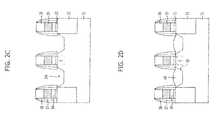
- FIGS. 2A to 2Eare diagrams illustrating a method for fabricating a semiconductor device having a strained channel in accordance with an embodiment of the present invention.
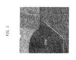
- FIG. 3is a picture showing an epitaxial film grown in accordance with an embodiment of the present invention.
- FIGS. 2A to 2Eare diagrams illustrating a method for fabricating a semiconductor device having a strained channel in accordance with an embodiment of the present invention.
- a field oxide layer 32is formed in a silicon substrate 31 to isolate one device from another.
- the field oxide layer 32may be formed using an STI process.
- the field oxide layer 32defines an active area.
- a gate pattern including a gate insulating layer 33 , a gate polysilicon layer 34 , a gate conductive layer 35 , and a gate hard mask layer 36is formed.
- a channel region Cis formed below the gate pattern.
- Gate spacers 37are formed on both sidewalls of the gate pattern.
- the gate spacers 37may be formed by depositing a spacer insulating layer and etching back the spacer insulating layer.
- the spacer insulating layer used for forming the gate spacers 37may be a single layer, such as a nitride layer or an oxide layer. Further, the spacer insulating layer may be a stacked layer including a nitride layer and an oxide layer.
- a dummy gate spacer 38is formed on a sidewall of each gate spacer 37 .
- the dummy gate spacers 38may be formed of material that can be removed by a following process.
- the dummy gate spacer 38may be formed of an oxide layer or a stacked layer including an oxide layer and a nitride layer.
- the dummy gate spacer 38is formed of an oxide layer.
- the dummy gate spacer 38may be formed by depositing an oxide layer and etching back the oxide layer.
- a width of the channel region Cbecomes smaller in proportion to a distance between dummy gate spacers 38 on the same gate pattern than in proportion to a distance between gate spacers 37 on the same gate pattern.
- the silicon substrate 31is placed in a thin film deposition apparatus for a selective epitaxial growth (SEG) process.
- SEGselective epitaxial growth
- the silicon substrate 31 under the dummy gate spacer 38is recessed at a predetermined depth by performing an isotropic etching using an etching gas in the thin film deposition apparatus.
- an In-Situ dry cleaning process and an In-Situ wet cleaning processmay be performed before the silicon substrate 31 is placed in the thin film deposition apparatus.
- both the In-Situ dry cleaning process and the In-Situ wet cleaning processmay be performed.
- Such In-Situ cleaning processesexpose a clean surface of a silicon substrate by removing a natural oxide layer and other surface pollutants.
- gas or solution having a proper selectivityis used during the In-Situ cleaning process.
- the In-Situ cleaning processis performed at a temperature ranging from a normal temperature to about 600° C.
- a recess region 39is formed to have a predetermined depth by performing isotropic etching.
- the recess region 39includes inclined sidewalls having a predetermined slope and a flat bottom surface. More specifically, the recess region 39 has an etching slope profile such that the inclined sidewall closest to the channel region C has a greater depth at points farther from the channel region C.
- An isotropic etching gassuch as hydrogen chloride HCl and chlorine Cl 2 may be used to isotropically etch the silicon substrate 31 thereby forming the recess 39 .
- the recess etchingmay be performed using a separate chamber under the condition that a following deposition process and a vacuum state are not disturbed. Further, the recess etching may be performed using an additional isotropic wet solution under the condition that a following deposition process and a vacuum state are not disturbed.
- the depth of the recess etchingmay be decided according to the amount of stress that may be applied to a channel necessary to obtain the desired device characteristics.
- the depth of the recess etchingis about 100 ⁇ to 1000 ⁇ .
- a lateral etching distance of recess etchingis controlled to be maximally recessed in consideration of a thickness of the gate spacer 37 , a channel length, and a height of the gate pattern.
- the recess etchingmay be controlled to form a recess region under the gate spacer 37 or the dummy gate spacer 38 . Further, the recess etching may be controlled, so that a side of the field oxide layer 32 is not exposed (i.e., the silicon substrate 31 continues to cover the side of the field oxide layer 32 ).
- an epitaxial film 40is formed in the recess region 39 by continuously performing a selective epitaxial growth process.
- the epitaxial film 40later becomes a source region and a drain region.
- the epitaxial film 40may be a single layer made of silicon-germanium (SiGe), a silicon carbon (SiC), or silicon-germanium-carbon (SiGeC).
- the epitaxial film 40may be a stacked layer formed of a silicon layer and a silicon-germanium layer, or a silicon-carbon layer and a silicon layer.
- a Boron doped epitaxial silicon-germanium layer(or a stacked layer of a silicon layer and a silicon-germanium layer) is used.
- the Boroncauses a compressive stress because the Boron includes a lattice constant higher than that of the silicon substrate thereby improving the mobility of the holes which act as carriers.
- phosphorus (P) or arsenic (AS) doped epitaxial silicon-carbon layer(or a stacked layer of a silicon layer and a silicon-carbon layer) is used.
- the epitaxial film 40may be formed using a Low Pressure CVD (LPCVD) apparatus, a Very Low Pressure CVD (VLPCVD) apparatus, a Plasma Enhanced-CVD (PE-CVD) apparatus, an Ultrahigh Vacuum CVD (UHVCVD) apparatus, a Rapid Thermal CVD (RTCVD) apparatus, an Atmosphere Pressure CVD (APCVD) apparatus, or a Molecular Beam Epitaxy (MBE) apparatus.
- LPCVDLow Pressure CVD
- VLPCVDVery Low Pressure CVD
- PE-CVDPlasma Enhanced-CVD
- UHVCVDUltrahigh Vacuum CVD
- RTCVDRapid Thermal CVD
- APCVDAtmosphere Pressure CVD
- MBEMolecular Beam Epitaxy
- the deposition temperature of the epitaxial film 40is in a range of about 400 to 800° C.
- a facetis not formed in the epitaxial film 40 if the epitaxial film 40 is grown by the selective epitaxial growth process as described above. Therefore, it is possible to control a dopant profile by using an In-Situ doping method or by performing a following ion implantation process without doping.
- the epitaxial film 40is formed to be higher than a lower part of the dummy gate spacer 38 . After forming the epitaxial film 40 , the dummy gate spacer 38 is removed. Accordingly, a surface area of the epitaxial film 40 is increased, so it is possible to reduce surface resistance.
- a size of a channel strain created by the epitaxial film 40increases in proportion to the increase of germanium concentration or carbon concentration, the increase of a bottom lateral depth of a gate space, and the increase of the recess depth.
- the germanium concentration or carbon concentrationis decided according to the device property. Preferably, the germanium concentration is about 5% to 50%, and the carbon concentration is about 0.1% to 10%.
- the epitaxial film 40is deposited at a predetermined thickness higher than a lower part of the dummy gate spacer 38 . Accordingly, the upper surface of the epitaxial film 40 becomes higher than the bottom surface of the gate spacer 37 after the dummy gate spacer 38 is removed.
- the thickness of the epitaxial film 40is decided according to a recess depth and the desired device characteristics. Preferably, the thickness of the epitaxial film 40 is in a range of about 100 ⁇ to about 2,000 ⁇ .
- the epitaxial film 40is doped through In-Situ doping.
- the epitaxial film 40may be doped through ion implantation in a subsequent process. Such an ion implantation process may be performed before or after removing the dummy gate spacer 38 .
- an interface defectis suppressed between the silicon substrate 31 and the epitaxial film 40 by continuously performing the recess etching and epitaxial film deposition. Further, the defect of the epitaxial film 40 is suppressed.
- a semiconductor device having a strained channelis completely manufactured by performing the following device manufacturing processes after removing the dummy gate spacer 38 .
- the dummy gate spacer 38may be removed right after depositing the epitaxial film 40 . Or, the dummy gate spacer 38 may be used to prevent additional ion implantation thereby reducing resistance and improving the short channel effect of the channel region C.
- silicidemay be formed by the following process.
- the surface resistance of the source region and the drain regioncan be reduced using titanium silicide (TiSi 2 ), cobalt silicide (CoSi2), and nickel silicide (NiSi).
- FIG. 3is a picture showing an epitaxial film grown in accordance with an embodiment of the present invention. As shown in FIG. 3 , an epitaxial film made of SiGe is formed without a facet being created around a field oxide layer. Further, the picture clearly shows a recess region leaving a predetermined amount of silicon substrate around the field oxide layer and having a predetermined slope.
- the In-Situ recess etchingis performed using an etching gate in a thin film deposition apparatus after forming the dummy gate spacer 38 made of a material that can be removed by a subsequent process. Accordingly, the short channel effect is suppressed by maximizing the strain channel effect while controlling a slope profile of the recess such that the recess becomes deeper at points further from the channel region. Further, the In-Situ recess etching prevents a facet from being generated around the field oxide layer and reduces the surface resistance due to an increase of the surface area of the epitaxial film 40 , which is exposed after removing the dummy gate spacer 38 . Therefore, a high quality epitaxial film 40 can be obtained by the In-Situ recess etching method according to the present embodiment.
- the removable dummy gate spacer 38is additionally formed after forming the gate spacers 37 . Then, the In-Situ isotropic recess etching is performed in a thin film deposition apparatus using an etching gas of hydrogen chloride HCl and chlorine Cl 2 . Accordingly, it is possible to suppress the short channel effect while maximizing channel strain effect by controlling an etching profile to form recesses 39 having inclined sides that slope towards each other as their depths increase.
- a facetis prevented from being formed by leaving a part of a silicon substrate 31 at a side of the field oxide layer 32 due to the recess etching. Moreover, the surface resistance can be reduced because the selective epitaxial thin film 40 surface exposed after removing the dummy gate spacer 38 increases compared with that of the related art.
- the recess regionis formed by the In-Situ recess etching in the thin film deposition apparatus before depositing the epitaxial film 40 .
- the recess regionis formed by the In-Situ recess etching in the thin film deposition apparatus before depositing the epitaxial film 40 .
- the present inventionrelates to a method for fabricating a semiconductor device, and more particularly, to a method for fabricating a semiconductor device having a strained channel.
- the method for manufacturing a semiconductor device having a strained channel according to the present inventioncan suppress short channel effect while maximizing strain effect by controlling an etching profile of a recess region using the dummy gate spacer 38 .
- a facetis prevented from being formed around the field oxide layer 32 by controlling the etching profile of the recess region 39 , and the surface resistance is reduced due to the increased surface area of the epitaxial film 40 , which is exposed after removing the dummy gate spacer 38 .
- the In-Situ recess etchingis performed in the thin film deposition apparatus before deposition, so the interface between the silicon substrate 31 and the epitaxial film 40 remains clean. Accordingly, a high quality epitaxial film 40 can be obtained, and it is possible to obtain a device with an improved junction leakage current property.
Landscapes
- Insulated Gate Type Field-Effect Transistor (AREA)
Abstract
Description
- The present application claims priority of Korean patent application number 10-2009-0060876, filed on Jul. 3, 2009, which is incorporated by reference in its entirety.
- The present invention relates to a method for fabricating a semiconductor device, and more particularly, to a method for fabricating a semiconductor device having a strained channel.
- Due to the high-integration of a semiconductor device, a gate insulating layer thickness and a channel length of a MOS device have been continuously reduced. Such reduction of the gate insulating layer thickness and the channel length increases the mobility of electrons or holes. That is, the reduction of the gate insulating layer thickness and the channel length improves the speed and operation current of a device.
- However, the reduction of a channel length disadvantageously causes short channel effect. Further, the reduction of the gate insulating layer thickness increases gate leakage current. In order to overcome the problem of the short channel effect, a large amount of impurities is doped in a channel. That is, the doped impurities disturb carrier movement. Accordingly, the doped impurities degrade the mobility of carriers although a channel length is reduced.
- In order to improve an operation speed and operation current of a device, many methods for increasing carrier mobility have been introduced. Particularly, a method for forming a strained channel has been receiving attention. The method for forming a strained channel according to the related art recesses a source/drain region around a gate side wall through etching and applies stress to a channel by selectively depositing an epitaxial thin film of group 4 elements having a lattice constant different from that of a silicon substrate.
- Hereinafter, a method for forming a strained channel by selectively filling the recessed source/drain region with epitaxial silicon-germanium (SiGe) or silicon-carbon (SiC) according to the related art will be described with reference to the accompanying drawings.
FIGS. 1A to 1D are diagrams illustrating a method for manufacturing a semiconductor device having a strained channel according to the related art.- As show in
FIG. 1A , afield oxide layer 12 is formed over asilicon substrate 11 to isolate one device from another. Then, a gate pattern is formed over thefield oxide layer 12. Here, the gate pattern includes agate insulating layer 13, agate polysilicon layer 14, a gateconductive layer 15, and a gatehard mask layer 16. - After forming the gate pattern,
gate spacers 17 are formed on both sidewalls of the gate pattern, and arecess region 18 is formed by recessing a predetermined region of source/drain regions to a predetermined depth. - As shown in
FIG. 1B , anepitaxial film 19 is formed over therecess region 18 through a selective epitaxial growth (SEG) process. Theepitaxial film 19 includes silicon-germanium (SiGe), silicon-carbon (SiC), or silicon-germanium-carbon (SiGeC) each having a lattice constant different from that of thesilicon substrate 11. - A size of a channel strain formed by the
epitaxial film 19 increases in proportion to the increase of germanium concentration or carbon concentration, the increase of a lateral width of the gate spacer, and the increase of a recess depth. - However, when a channel length becomes short due to the high integration of a device, or when a deep recess is formed and In-Situ doping is performed, a junction depth becomes significantly large. Accordingly, device characteristics may be degraded due to a short channel effect. In other words, although a recess depth should be deep for obtaining a strained channel effect, the short channel effect becomes worse in proportion to the recess depth. Accordingly, there is a limitation on the recess depth that may be utilized.
- In order to overcome such a short channel effect problem, an impurity doped
epitaxial film 21A is formed by performing ion implantation (see arrow ofFIG. 1C ) after depositing an un-dopedepitaxial film 20 as shown inFIGS. 1C and 1D . In another method (not shown in the accompanying drawings), an un-doped epitaxial film is partially deposited and a stack is formed at a remaining part through In-Situ doping. However, each of these methods have the following shortcomings. - In the method of performing ion implantation after depositing un-doped
epitaxial film 20, it is difficult to control an ion-implantation depth and profile due to a facet formed around afield oxide layer 12. That is, an inability to control the implantation depth forms a doping profile, as shown inFIG. 1D , because of the facet formed around thefield oxide layer 12 of the un-doped epitaxial film20 (shown inFIG. 1C ). Accordingly, the device characteristics are degraded due to the short channel effect and an increase of the junction leakage current. - The method of partially depositing un-doped epitaxial film and depositing In-Situ doped epitaxial film as deep as a junction depth slightly overcomes the short channel effect problem and junction leakage current problem. However, this method does not entirely overcome the difficulty of controlling the doping profile because the facet is still created. In the case of a DRAM for storing data, the number of transistors at a peripheral circuit is abruptly increased according to an increase of the integration degree. Accordingly, a distance between a gate pattern and an
adjacent field oxide 12 layer becomes close. Thus, the existence of a facet significantly contributes to the short channel effect problem. Therefore, this method also does not overcome the above problems. - Embodiments of the present invention are directed to providing a method for manufacturing a semiconductor device capable of suppressing short channel effect while maximizing strained channel effect.
- Embodiments of the present invention are directed to providing a method for manufacturing a semiconductor device capable of preventing a facet from being generated around a field oxide layer when an epitaxial film is formed in a recess region for a strained channel.
- In accordance with an aspect of the present invention, there is provided a method for forming a semiconductor device, including forming a gate pattern over a silicon substrate, forming gate spacers over both sidewalls of the gate pattern, forming a dummy gate spacer over a sidewall of each one of the gate spacers, forming a recess region having inclined sidewalls extending in a direction to a channel region under the gate pattern by recess-etching the silicon substrate, filling the recess region with an epitaxial film that becomes a source region or a drain region through a selective epitaxial growth process, and removing the dummy gate spacer.
- In accordance with a further aspect of the present invention, there is provided a method for fabricating a semiconductor device including forming a gate pattern over a silicon substrate having a field oxide layer, forming gate spacers over both sidewalls of the gate pattern, forming a dummy gate spacer over a sidewall of each one of the gate spacers, forming a recess region having inclined sidewalls having a predetermined slope by recess-etching the silicon substrate between the dummy gate spacer and the field oxide layer, filling the recess region with an epitaxial film through a selective epitaxial growth process, wherein the epitaxial film becomes a source region and a drain region, and removing the dummy gate spacer.
FIGS. 1A to 1D are diagrams illustrating a method for fabricating a semiconductor device having a strained channel according to the related art.FIGS. 2A to 2E are diagrams illustrating a method for fabricating a semiconductor device having a strained channel in accordance with an embodiment of the present invention.FIG. 3 is a picture showing an epitaxial film grown in accordance with an embodiment of the present invention.- Other objects and advantages of the present invention can be understood by the following description, and become apparent with reference to the embodiments of the present invention.
FIGS. 2A to 2E are diagrams illustrating a method for fabricating a semiconductor device having a strained channel in accordance with an embodiment of the present invention.- As shown in
FIG. 2A , afield oxide layer 32 is formed in asilicon substrate 31 to isolate one device from another. Thefield oxide layer 32 may be formed using an STI process. Thefield oxide layer 32 defines an active area. - A gate pattern including a
gate insulating layer 33, agate polysilicon layer 34, a gateconductive layer 35, and a gatehard mask layer 36 is formed. A channel region C is formed below the gate pattern. Gate spacers 37 are formed on both sidewalls of the gate pattern. The gate spacers37 may be formed by depositing a spacer insulating layer and etching back the spacer insulating layer.- The spacer insulating layer used for forming the
gate spacers 37 may be a single layer, such as a nitride layer or an oxide layer. Further, the spacer insulating layer may be a stacked layer including a nitride layer and an oxide layer. - As shown in
FIG. 2B , adummy gate spacer 38 is formed on a sidewall of eachgate spacer 37. Thedummy gate spacers 38 may be formed of material that can be removed by a following process. For example, thedummy gate spacer 38 may be formed of an oxide layer or a stacked layer including an oxide layer and a nitride layer. Although, preferably, thedummy gate spacer 38 is formed of an oxide layer. Thedummy gate spacer 38 may be formed by depositing an oxide layer and etching back the oxide layer. - If the
dummy gate spacers 38 are formed as shown inFIG. 2B , a width of the channel region C becomes smaller in proportion to a distance betweendummy gate spacers 38 on the same gate pattern than in proportion to a distance betweengate spacers 37 on the same gate pattern. - As shown in
FIG. 2C , thesilicon substrate 31 is placed in a thin film deposition apparatus for a selective epitaxial growth (SEG) process. - Then, the
silicon substrate 31 under thedummy gate spacer 38 is recessed at a predetermined depth by performing an isotropic etching using an etching gas in the thin film deposition apparatus. Before thesilicon substrate 31 is placed in the thin film deposition apparatus, one of an In-Situ dry cleaning process and an In-Situ wet cleaning process may be performed. Or, both the In-Situ dry cleaning process and the In-Situ wet cleaning process may be performed. Such In-Situ cleaning processes expose a clean surface of a silicon substrate by removing a natural oxide layer and other surface pollutants. In order to minimize the loss of thegate spacer 37 and thedummy gate spacer 38, gas or solution having a proper selectivity is used during the In-Situ cleaning process. The In-Situ cleaning process is performed at a temperature ranging from a normal temperature to about 600° C. - As described above, a
recess region 39 is formed to have a predetermined depth by performing isotropic etching. Therecess region 39 includes inclined sidewalls having a predetermined slope and a flat bottom surface. More specifically, therecess region 39 has an etching slope profile such that the inclined sidewall closest to the channel region C has a greater depth at points farther from the channel region C. - An isotropic etching gas, such as hydrogen chloride HCl and chlorine Cl2may be used to isotropically etch the
silicon substrate 31 thereby forming therecess 39. - The recess etching may be performed using a separate chamber under the condition that a following deposition process and a vacuum state are not disturbed. Further, the recess etching may be performed using an additional isotropic wet solution under the condition that a following deposition process and a vacuum state are not disturbed.
- The depth of the recess etching may be decided according to the amount of stress that may be applied to a channel necessary to obtain the desired device characteristics. Preferably, the depth of the recess etching is about 100 Å to 1000 Å.
- A lateral etching distance of recess etching is controlled to be maximally recessed in consideration of a thickness of the
gate spacer 37, a channel length, and a height of the gate pattern. - The recess etching may be controlled to form a recess region under the
gate spacer 37 or thedummy gate spacer 38. Further, the recess etching may be controlled, so that a side of thefield oxide layer 32 is not exposed (i.e., thesilicon substrate 31 continues to cover the side of the field oxide layer32). - After the recess etching, an
epitaxial film 40 is formed in therecess region 39 by continuously performing a selective epitaxial growth process. Theepitaxial film 40 later becomes a source region and a drain region. Theepitaxial film 40 may be a single layer made of silicon-germanium (SiGe), a silicon carbon (SiC), or silicon-germanium-carbon (SiGeC). Alternatively, theepitaxial film 40 may be a stacked layer formed of a silicon layer and a silicon-germanium layer, or a silicon-carbon layer and a silicon layer. In the case of a PMOS device, a Boron doped epitaxial silicon-germanium layer (or a stacked layer of a silicon layer and a silicon-germanium layer) is used. The Boron causes a compressive stress because the Boron includes a lattice constant higher than that of the silicon substrate thereby improving the mobility of the holes which act as carriers. In the case of an NMOS device, phosphorus (P) or arsenic (AS) doped epitaxial silicon-carbon layer (or a stacked layer of a silicon layer and a silicon-carbon layer) is used. Both the phosphorus (P) and the arsenic (AS) cause tensile stress because the phosphorus and the arsenic both have a lattice constant smaller than that of the silicon substrate thereby improving the mobility of the electrons which act as carriers. - The
epitaxial film 40 may be formed using a Low Pressure CVD (LPCVD) apparatus, a Very Low Pressure CVD (VLPCVD) apparatus, a Plasma Enhanced-CVD (PE-CVD) apparatus, an Ultrahigh Vacuum CVD (UHVCVD) apparatus, a Rapid Thermal CVD (RTCVD) apparatus, an Atmosphere Pressure CVD (APCVD) apparatus, or a Molecular Beam Epitaxy (MBE) apparatus. - The deposition temperature of the
epitaxial film 40 is in a range of about 400 to 800° C. - A facet is not formed in the
epitaxial film 40 if theepitaxial film 40 is grown by the selective epitaxial growth process as described above. Therefore, it is possible to control a dopant profile by using an In-Situ doping method or by performing a following ion implantation process without doping. - The
epitaxial film 40 is formed to be higher than a lower part of thedummy gate spacer 38. After forming theepitaxial film 40, thedummy gate spacer 38 is removed. Accordingly, a surface area of theepitaxial film 40 is increased, so it is possible to reduce surface resistance. - A size of a channel strain created by the
epitaxial film 40 increases in proportion to the increase of germanium concentration or carbon concentration, the increase of a bottom lateral depth of a gate space, and the increase of the recess depth. The germanium concentration or carbon concentration is decided according to the device property. Preferably, the germanium concentration is about 5% to 50%, and the carbon concentration is about 0.1% to 10%. - The
epitaxial film 40 is deposited at a predetermined thickness higher than a lower part of thedummy gate spacer 38. Accordingly, the upper surface of theepitaxial film 40 becomes higher than the bottom surface of thegate spacer 37 after thedummy gate spacer 38 is removed. The thickness of theepitaxial film 40 is decided according to a recess depth and the desired device characteristics. Preferably, the thickness of theepitaxial film 40 is in a range of about 100 Å to about 2,000 Å. - The
epitaxial film 40 is doped through In-Situ doping. Alternatively, theepitaxial film 40 may be doped through ion implantation in a subsequent process. Such an ion implantation process may be performed before or after removing thedummy gate spacer 38. - As shown in
FIGS. 2C and 2D , an interface defect is suppressed between thesilicon substrate 31 and theepitaxial film 40 by continuously performing the recess etching and epitaxial film deposition. Further, the defect of theepitaxial film 40 is suppressed. - As shown in
FIG. 2E , a semiconductor device having a strained channel is completely manufactured by performing the following device manufacturing processes after removing thedummy gate spacer 38. - The
dummy gate spacer 38 may be removed right after depositing theepitaxial film 40. Or, thedummy gate spacer 38 may be used to prevent additional ion implantation thereby reducing resistance and improving the short channel effect of the channel region C. - Further, silicide may be formed by the following process. The surface resistance of the source region and the drain region can be reduced using titanium silicide (TiSi2), cobalt silicide (CoSi2), and nickel silicide (NiSi).
FIG. 3 is a picture showing an epitaxial film grown in accordance with an embodiment of the present invention. As shown inFIG. 3 , an epitaxial film made of SiGe is formed without a facet being created around a field oxide layer. Further, the picture clearly shows a recess region leaving a predetermined amount of silicon substrate around the field oxide layer and having a predetermined slope.- As described above, the In-Situ recess etching is performed using an etching gate in a thin film deposition apparatus after forming the
dummy gate spacer 38 made of a material that can be removed by a subsequent process. Accordingly, the short channel effect is suppressed by maximizing the strain channel effect while controlling a slope profile of the recess such that the recess becomes deeper at points further from the channel region. Further, the In-Situ recess etching prevents a facet from being generated around the field oxide layer and reduces the surface resistance due to an increase of the surface area of theepitaxial film 40, which is exposed after removing thedummy gate spacer 38. Therefore, a highquality epitaxial film 40 can be obtained by the In-Situ recess etching method according to the present embodiment. - In the embodiments of the present invention, the removable
dummy gate spacer 38 is additionally formed after forming thegate spacers 37. Then, the In-Situ isotropic recess etching is performed in a thin film deposition apparatus using an etching gas of hydrogen chloride HCl and chlorine Cl2. Accordingly, it is possible to suppress the short channel effect while maximizing channel strain effect by controlling an etching profile to formrecesses 39 having inclined sides that slope towards each other as their depths increase. - Further, a facet is prevented from being formed by leaving a part of a
silicon substrate 31 at a side of thefield oxide layer 32 due to the recess etching. Moreover, the surface resistance can be reduced because the selective epitaxialthin film 40 surface exposed after removing thedummy gate spacer 38 increases compared with that of the related art. - Unlike the related art, the recess region is formed by the In-Situ recess etching in the thin film deposition apparatus before depositing the
epitaxial film 40. Thus, it is possible to sustain a clean interface between thesubstrate 31 and thethin film 40. Therefore, a high quality selective epitaxialthin film 40 can be obtained as well as an improved junction leakage current. - Further, it is possible to shorten a fabrication time by performing a recess etching process and a deposition process as one process.
- The present invention relates to a method for fabricating a semiconductor device, and more particularly, to a method for fabricating a semiconductor device having a strained channel. As described above, the method for manufacturing a semiconductor device having a strained channel according to the present invention can suppress short channel effect while maximizing strain effect by controlling an etching profile of a recess region using the
dummy gate spacer 38. - Further, a facet is prevented from being formed around the
field oxide layer 32 by controlling the etching profile of therecess region 39, and the surface resistance is reduced due to the increased surface area of theepitaxial film 40, which is exposed after removing thedummy gate spacer 38. - Moreover, unlike the related art, the In-Situ recess etching is performed in the thin film deposition apparatus before deposition, so the interface between the
silicon substrate 31 and theepitaxial film 40 remains clean. Accordingly, a highquality epitaxial film 40 can be obtained, and it is possible to obtain a device with an improved junction leakage current property. - While the present invention has been described with respect to the specific embodiments, it will be apparent to those skilled in the art that various changes and modifications may be made without departing from the spirit and scope of the invention as defined in the following claims.
Claims (16)
1. A method for forming a semiconductor device, comprising:
forming a gate pattern over a silicon substrate;
forming gate spacers over both sidewalls of the gate pattern;
forming a dummy gate spacer over a sidewall of each one of the gate spacers;
forming a recess region having inclined sidewalls extending in a direction to a channel region under the gate pattern by recess-etching the silicon substrate;
filling the recess region with an epitaxial film for a source region or a drain region through a selective epitaxial growth process; and
removing the dummy gate spacer.
2. The method ofclaim 1 , wherein each inclined sidewall of the recess region closest to the channel region under the gate pattern has a greater depth at points farther from the channel region.
3. The method ofclaim 1 , wherein the dummy gate spacer comprises an oxide layer.
4. The method ofclaim 1 , wherein the forming of the recess region is performed by an isotropic etching.
5. The method ofclaim 1 , wherein the forming of the recess region comprises performing In-Situ recess etching on the silicon substrate in a deposition apparatus used for the selective epitaxial growth process.
6. The method ofclaim 5 , wherein a cleaning process is performed before the silicon substrate is placed in the deposition apparatus used for the selective epitaxial growth process.
7. The method ofclaim 1 , wherein the epitaxial film is grown to have a thickness higher than an interface between the dummy gate spacer and the silicon substrate during the selective epitaxial growth process.
8. The method ofclaim 1 , wherein the epitaxial film is one selected from a group consisting of a silicon-germanium layer, a silicon carbon layer, and a silicon-germanium-carbon layer.
9. A method for fabricating a semiconductor device, comprising:
forming a gate pattern over a silicon substrate having a field oxide layer;
forming gate spacers over both sidewalls of the gate pattern;
forming a dummy gate spacer over a sidewall of each one of the gate spacers;
forming a recess region having inclined sidewalls having a predetermined slope by recess-etching the silicon substrate between the dummy gate spacer and the field oxide layer;
filling the recess region with an epitaxial film through a selective epitaxial growth process, wherein the epitaxial film becomes a source region and a drain region; and
removing the dummy gate spacer.
10. The method ofclaim 9 , wherein the inclined sidewall closest to a channel region under the gate pattern has a greater depth at points farther from the channel region.
11. The method ofclaim 9 , wherein the dummy gate spacer comprises an oxide layer.
12. The method ofclaim 9 , wherein the forming of the recess region is performed by an isotropic etching.
13. The method ofclaim 9 , wherein the forming of the recess region comprises performing In-Situ recess etching on the silicon substrate in a deposition apparatus used for the selective epitaxial growth process.
14. The method ofclaim 13 , wherein a cleaning process is performed before placing the silicon substrate in the deposition apparatus used for the selective epitaxial growth process.
15. The method ofclaim 9 , wherein the epitaxial film is grown to have a predetermined thickness higher than an interface between the dummy gate spacer and the silicon substrate during the selective epitaxial growth process.
16. The method ofclaim 9 , wherein the epitaxial film is one selected from a group consisting of a silicon-germanium layer, a silicon carbon layer, and a silicon-germanium-carbon layer.
Applications Claiming Priority (2)
| Application Number | Priority Date | Filing Date | Title |
|---|---|---|---|
| KR1020090060876AKR101050405B1 (en) | 2009-07-03 | 2009-07-03 | Method of manufacturing semiconductor device having strained channel |
| KR10-2009-0060876 | 2009-07-03 |
Publications (1)
| Publication Number | Publication Date |
|---|---|
| US20110003450A1true US20110003450A1 (en) | 2011-01-06 |
Family
ID=43412907
Family Applications (1)
| Application Number | Title | Priority Date | Filing Date |
|---|---|---|---|
| US12/646,207AbandonedUS20110003450A1 (en) | 2009-07-03 | 2009-12-23 | Method for manufacturing semicondutor device with strained channel |
Country Status (2)
| Country | Link |
|---|---|
| US (1) | US20110003450A1 (en) |
| KR (1) | KR101050405B1 (en) |
Cited By (288)
| Publication number | Priority date | Publication date | Assignee | Title |
|---|---|---|---|---|
| US20100289116A1 (en)* | 2009-05-12 | 2010-11-18 | Taiwan Semiconductor Manufacturing Company, Ltd. | Selective Epitaxial Growth of Semiconductor Materials with Reduced Defects |
| US20110316046A1 (en)* | 2010-06-29 | 2011-12-29 | Globalfoundries Inc. | Field Effect Transistor Device |
| US20120217583A1 (en)* | 2010-10-28 | 2012-08-30 | Huilong Zhu | Semiconductor device and method for forming the same |
| US20130119444A1 (en)* | 2011-11-15 | 2013-05-16 | Taiwan Semiconductor Manufacturing Company, Ltd. | Semiconductor device and method of manufacturing the same |
| WO2015027141A1 (en) | 2013-08-22 | 2015-02-26 | Texas Instruments Incorporated | Improved silicide formation by improved sige faceting |
| US20150179796A1 (en)* | 2013-12-19 | 2015-06-25 | Taiwan Semiconductor Manufacturing Co., Ltd. | Germanium Profile for Channel Strain |
| US9117910B2 (en) | 2013-06-25 | 2015-08-25 | Samsung Electronics Co., Ltd. | Semiconductor device and fabricating method thereof |
| KR20160011301A (en)* | 2014-07-21 | 2016-02-01 | 삼성전자주식회사 | Method of fabricating semiconductor devices |
| US20170194176A1 (en)* | 2015-12-30 | 2017-07-06 | Taiwan Semiconductor Manufacturing Co., Ltd. | Control wafer making device and method for measuring and monitoring control wafer |
| US9711505B2 (en) | 2015-07-28 | 2017-07-18 | Samsung Electronics Co., Ltd. | Semiconductor devices having dummy gate structure for controlling channel stress |
| US9911805B2 (en)* | 2013-03-15 | 2018-03-06 | Taiwan Semiconductor Manufacturing Co., Ltd. | Silicon recess etch and epitaxial deposit for shallow trench isolation (STI) |
| US10811516B2 (en)* | 2014-12-24 | 2020-10-20 | Taiwan Semiconductor Manufacturing Company, Ltd. | Structure and formation method of semiconductor device structure with gate stack |
| KR20210016091A (en)* | 2018-07-05 | 2021-02-10 | 어플라이드 머티어리얼스, 인코포레이티드 | Integrated CMOS Source Drain Formation Using Advanced Control |
| US11001925B2 (en) | 2016-12-19 | 2021-05-11 | Asm Ip Holding B.V. | Substrate processing apparatus |
| US11004977B2 (en) | 2017-07-19 | 2021-05-11 | Asm Ip Holding B.V. | Method for depositing a group IV semiconductor and related semiconductor device structures |
| US11018002B2 (en) | 2017-07-19 | 2021-05-25 | Asm Ip Holding B.V. | Method for selectively depositing a Group IV semiconductor and related semiconductor device structures |
| US11015245B2 (en) | 2014-03-19 | 2021-05-25 | Asm Ip Holding B.V. | Gas-phase reactor and system having exhaust plenum and components thereof |
| US11022879B2 (en) | 2017-11-24 | 2021-06-01 | Asm Ip Holding B.V. | Method of forming an enhanced unexposed photoresist layer |
| US11031242B2 (en) | 2018-11-07 | 2021-06-08 | Asm Ip Holding B.V. | Methods for depositing a boron doped silicon germanium film |
| USD922229S1 (en) | 2019-06-05 | 2021-06-15 | Asm Ip Holding B.V. | Device for controlling a temperature of a gas supply unit |
| US11049751B2 (en) | 2018-09-14 | 2021-06-29 | Asm Ip Holding B.V. | Cassette supply system to store and handle cassettes and processing apparatus equipped therewith |
| US11056344B2 (en) | 2017-08-30 | 2021-07-06 | Asm Ip Holding B.V. | Layer forming method |
| US11053591B2 (en) | 2018-08-06 | 2021-07-06 | Asm Ip Holding B.V. | Multi-port gas injection system and reactor system including same |
| US11069510B2 (en) | 2017-08-30 | 2021-07-20 | Asm Ip Holding B.V. | Substrate processing apparatus |
| US11081345B2 (en) | 2018-02-06 | 2021-08-03 | Asm Ip Holding B.V. | Method of post-deposition treatment for silicon oxide film |
| US11088002B2 (en) | 2018-03-29 | 2021-08-10 | Asm Ip Holding B.V. | Substrate rack and a substrate processing system and method |
| US11087997B2 (en) | 2018-10-31 | 2021-08-10 | Asm Ip Holding B.V. | Substrate processing apparatus for processing substrates |
| US11094546B2 (en) | 2017-10-05 | 2021-08-17 | Asm Ip Holding B.V. | Method for selectively depositing a metallic film on a substrate |
| US11094582B2 (en) | 2016-07-08 | 2021-08-17 | Asm Ip Holding B.V. | Selective deposition method to form air gaps |
| US11101370B2 (en) | 2016-05-02 | 2021-08-24 | Asm Ip Holding B.V. | Method of forming a germanium oxynitride film |
| US11107676B2 (en) | 2016-07-28 | 2021-08-31 | Asm Ip Holding B.V. | Method and apparatus for filling a gap |
| US11114294B2 (en) | 2019-03-08 | 2021-09-07 | Asm Ip Holding B.V. | Structure including SiOC layer and method of forming same |
| US11114283B2 (en) | 2018-03-16 | 2021-09-07 | Asm Ip Holding B.V. | Reactor, system including the reactor, and methods of manufacturing and using same |
| USD930782S1 (en) | 2019-08-22 | 2021-09-14 | Asm Ip Holding B.V. | Gas distributor |
| US11127589B2 (en) | 2019-02-01 | 2021-09-21 | Asm Ip Holding B.V. | Method of topology-selective film formation of silicon oxide |
| US11127617B2 (en) | 2017-11-27 | 2021-09-21 | Asm Ip Holding B.V. | Storage device for storing wafer cassettes for use with a batch furnace |
| USD931978S1 (en) | 2019-06-27 | 2021-09-28 | Asm Ip Holding B.V. | Showerhead vacuum transport |
| US11139191B2 (en) | 2017-08-09 | 2021-10-05 | Asm Ip Holding B.V. | Storage apparatus for storing cassettes for substrates and processing apparatus equipped therewith |
| US11139308B2 (en) | 2015-12-29 | 2021-10-05 | Asm Ip Holding B.V. | Atomic layer deposition of III-V compounds to form V-NAND devices |
| US11158513B2 (en) | 2018-12-13 | 2021-10-26 | Asm Ip Holding B.V. | Methods for forming a rhenium-containing film on a substrate by a cyclical deposition process and related semiconductor device structures |
| US11164955B2 (en) | 2017-07-18 | 2021-11-02 | Asm Ip Holding B.V. | Methods for forming a semiconductor device structure and related semiconductor device structures |
| USD935572S1 (en) | 2019-05-24 | 2021-11-09 | Asm Ip Holding B.V. | Gas channel plate |
| US11171025B2 (en) | 2019-01-22 | 2021-11-09 | Asm Ip Holding B.V. | Substrate processing device |
| US11168395B2 (en) | 2018-06-29 | 2021-11-09 | Asm Ip Holding B.V. | Temperature-controlled flange and reactor system including same |
| US11205585B2 (en) | 2016-07-28 | 2021-12-21 | Asm Ip Holding B.V. | Substrate processing apparatus and method of operating the same |
| US11217444B2 (en) | 2018-11-30 | 2022-01-04 | Asm Ip Holding B.V. | Method for forming an ultraviolet radiation responsive metal oxide-containing film |
| USD940837S1 (en) | 2019-08-22 | 2022-01-11 | Asm Ip Holding B.V. | Electrode |
| US11222772B2 (en) | 2016-12-14 | 2022-01-11 | Asm Ip Holding B.V. | Substrate processing apparatus |
| US11227782B2 (en) | 2019-07-31 | 2022-01-18 | Asm Ip Holding B.V. | Vertical batch furnace assembly |
| US11227789B2 (en) | 2019-02-20 | 2022-01-18 | Asm Ip Holding B.V. | Method and apparatus for filling a recess formed within a substrate surface |
| US11230766B2 (en) | 2018-03-29 | 2022-01-25 | Asm Ip Holding B.V. | Substrate processing apparatus and method |
| US11232963B2 (en) | 2018-10-03 | 2022-01-25 | Asm Ip Holding B.V. | Substrate processing apparatus and method |
| US11233133B2 (en) | 2015-10-21 | 2022-01-25 | Asm Ip Holding B.V. | NbMC layers |
| US11244825B2 (en) | 2018-11-16 | 2022-02-08 | Asm Ip Holding B.V. | Methods for depositing a transition metal chalcogenide film on a substrate by a cyclical deposition process |
| US11242598B2 (en) | 2015-06-26 | 2022-02-08 | Asm Ip Holding B.V. | Structures including metal carbide material, devices including the structures, and methods of forming same |
| US11251040B2 (en) | 2019-02-20 | 2022-02-15 | Asm Ip Holding B.V. | Cyclical deposition method including treatment step and apparatus for same |
| US11251068B2 (en) | 2018-10-19 | 2022-02-15 | Asm Ip Holding B.V. | Substrate processing apparatus and substrate processing method |
| US11251035B2 (en) | 2016-12-22 | 2022-02-15 | Asm Ip Holding B.V. | Method of forming a structure on a substrate |
| USD944946S1 (en) | 2019-06-14 | 2022-03-01 | Asm Ip Holding B.V. | Shower plate |
| US11270899B2 (en) | 2018-06-04 | 2022-03-08 | Asm Ip Holding B.V. | Wafer handling chamber with moisture reduction |
| US11274369B2 (en) | 2018-09-11 | 2022-03-15 | Asm Ip Holding B.V. | Thin film deposition method |
| US11282698B2 (en) | 2019-07-19 | 2022-03-22 | Asm Ip Holding B.V. | Method of forming topology-controlled amorphous carbon polymer film |
| US11286562B2 (en) | 2018-06-08 | 2022-03-29 | Asm Ip Holding B.V. | Gas-phase chemical reactor and method of using same |
| US11286558B2 (en) | 2019-08-23 | 2022-03-29 | Asm Ip Holding B.V. | Methods for depositing a molybdenum nitride film on a surface of a substrate by a cyclical deposition process and related semiconductor device structures including a molybdenum nitride film |
| US11289326B2 (en) | 2019-05-07 | 2022-03-29 | Asm Ip Holding B.V. | Method for reforming amorphous carbon polymer film |
| USD947913S1 (en) | 2019-05-17 | 2022-04-05 | Asm Ip Holding B.V. | Susceptor shaft |
| US11296189B2 (en) | 2018-06-21 | 2022-04-05 | Asm Ip Holding B.V. | Method for depositing a phosphorus doped silicon arsenide film and related semiconductor device structures |
| US11295980B2 (en) | 2017-08-30 | 2022-04-05 | Asm Ip Holding B.V. | Methods for depositing a molybdenum metal film over a dielectric surface of a substrate by a cyclical deposition process and related semiconductor device structures |
| USD948463S1 (en) | 2018-10-24 | 2022-04-12 | Asm Ip Holding B.V. | Susceptor for semiconductor substrate supporting apparatus |
| USD949319S1 (en) | 2019-08-22 | 2022-04-19 | Asm Ip Holding B.V. | Exhaust duct |
| US11306395B2 (en) | 2017-06-28 | 2022-04-19 | Asm Ip Holding B.V. | Methods for depositing a transition metal nitride film on a substrate by atomic layer deposition and related deposition apparatus |
| US11315794B2 (en) | 2019-10-21 | 2022-04-26 | Asm Ip Holding B.V. | Apparatus and methods for selectively etching films |
| US11339476B2 (en) | 2019-10-08 | 2022-05-24 | Asm Ip Holding B.V. | Substrate processing device having connection plates, substrate processing method |
| US11342216B2 (en) | 2019-02-20 | 2022-05-24 | Asm Ip Holding B.V. | Cyclical deposition method and apparatus for filling a recess formed within a substrate surface |
| US11345999B2 (en) | 2019-06-06 | 2022-05-31 | Asm Ip Holding B.V. | Method of using a gas-phase reactor system including analyzing exhausted gas |
| US11355338B2 (en) | 2019-05-10 | 2022-06-07 | Asm Ip Holding B.V. | Method of depositing material onto a surface and structure formed according to the method |
| US11361990B2 (en) | 2018-05-28 | 2022-06-14 | Asm Ip Holding B.V. | Substrate processing method and device manufactured by using the same |
| US11374112B2 (en) | 2017-07-19 | 2022-06-28 | Asm Ip Holding B.V. | Method for depositing a group IV semiconductor and related semiconductor device structures |
| US11378337B2 (en) | 2019-03-28 | 2022-07-05 | Asm Ip Holding B.V. | Door opener and substrate processing apparatus provided therewith |
| US11387120B2 (en) | 2017-09-28 | 2022-07-12 | Asm Ip Holding B.V. | Chemical dispensing apparatus and methods for dispensing a chemical to a reaction chamber |
| US11387106B2 (en) | 2018-02-14 | 2022-07-12 | Asm Ip Holding B.V. | Method for depositing a ruthenium-containing film on a substrate by a cyclical deposition process |
| US11390945B2 (en) | 2019-07-03 | 2022-07-19 | Asm Ip Holding B.V. | Temperature control assembly for substrate processing apparatus and method of using same |
| US11390946B2 (en) | 2019-01-17 | 2022-07-19 | Asm Ip Holding B.V. | Methods of forming a transition metal containing film on a substrate by a cyclical deposition process |
| US11393690B2 (en) | 2018-01-19 | 2022-07-19 | Asm Ip Holding B.V. | Deposition method |
| US11390950B2 (en) | 2017-01-10 | 2022-07-19 | Asm Ip Holding B.V. | Reactor system and method to reduce residue buildup during a film deposition process |
| US11396702B2 (en) | 2016-11-15 | 2022-07-26 | Asm Ip Holding B.V. | Gas supply unit and substrate processing apparatus including the gas supply unit |
| US11398382B2 (en) | 2018-03-27 | 2022-07-26 | Asm Ip Holding B.V. | Method of forming an electrode on a substrate and a semiconductor device structure including an electrode |
| US11401605B2 (en) | 2019-11-26 | 2022-08-02 | Asm Ip Holding B.V. | Substrate processing apparatus |
| US11410851B2 (en) | 2017-02-15 | 2022-08-09 | Asm Ip Holding B.V. | Methods for forming a metallic film on a substrate by cyclical deposition and related semiconductor device structures |
| US11414760B2 (en) | 2018-10-08 | 2022-08-16 | Asm Ip Holding B.V. | Substrate support unit, thin film deposition apparatus including the same, and substrate processing apparatus including the same |
| US11417545B2 (en) | 2017-08-08 | 2022-08-16 | Asm Ip Holding B.V. | Radiation shield |
| US11424119B2 (en) | 2019-03-08 | 2022-08-23 | Asm Ip Holding B.V. | Method for selective deposition of silicon nitride layer and structure including selectively-deposited silicon nitride layer |
| US11430640B2 (en) | 2019-07-30 | 2022-08-30 | Asm Ip Holding B.V. | Substrate processing apparatus |
| US11430674B2 (en) | 2018-08-22 | 2022-08-30 | Asm Ip Holding B.V. | Sensor array, apparatus for dispensing a vapor phase reactant to a reaction chamber and related methods |
| US11437241B2 (en) | 2020-04-08 | 2022-09-06 | Asm Ip Holding B.V. | Apparatus and methods for selectively etching silicon oxide films |
| US11443926B2 (en) | 2019-07-30 | 2022-09-13 | Asm Ip Holding B.V. | Substrate processing apparatus |
| US11447861B2 (en) | 2016-12-15 | 2022-09-20 | Asm Ip Holding B.V. | Sequential infiltration synthesis apparatus and a method of forming a patterned structure |
| US11447864B2 (en) | 2019-04-19 | 2022-09-20 | Asm Ip Holding B.V. | Layer forming method and apparatus |
| US11453943B2 (en) | 2016-05-25 | 2022-09-27 | Asm Ip Holding B.V. | Method for forming carbon-containing silicon/metal oxide or nitride film by ALD using silicon precursor and hydrocarbon precursor |
| USD965044S1 (en) | 2019-08-19 | 2022-09-27 | Asm Ip Holding B.V. | Susceptor shaft |
| USD965524S1 (en) | 2019-08-19 | 2022-10-04 | Asm Ip Holding B.V. | Susceptor support |
| US11469098B2 (en) | 2018-05-08 | 2022-10-11 | Asm Ip Holding B.V. | Methods for depositing an oxide film on a substrate by a cyclical deposition process and related device structures |
| US11476109B2 (en) | 2019-06-11 | 2022-10-18 | Asm Ip Holding B.V. | Method of forming an electronic structure using reforming gas, system for performing the method, and structure formed using the method |
| US11473195B2 (en) | 2018-03-01 | 2022-10-18 | Asm Ip Holding B.V. | Semiconductor processing apparatus and a method for processing a substrate |
| US11482418B2 (en) | 2018-02-20 | 2022-10-25 | Asm Ip Holding B.V. | Substrate processing method and apparatus |
| US11482412B2 (en) | 2018-01-19 | 2022-10-25 | Asm Ip Holding B.V. | Method for depositing a gap-fill layer by plasma-assisted deposition |
| US11482533B2 (en) | 2019-02-20 | 2022-10-25 | Asm Ip Holding B.V. | Apparatus and methods for plug fill deposition in 3-D NAND applications |
| US11488819B2 (en) | 2018-12-04 | 2022-11-01 | Asm Ip Holding B.V. | Method of cleaning substrate processing apparatus |
| US11488854B2 (en) | 2020-03-11 | 2022-11-01 | Asm Ip Holding B.V. | Substrate handling device with adjustable joints |
| US11495459B2 (en) | 2019-09-04 | 2022-11-08 | Asm Ip Holding B.V. | Methods for selective deposition using a sacrificial capping layer |
| US11492703B2 (en) | 2018-06-27 | 2022-11-08 | Asm Ip Holding B.V. | Cyclic deposition methods for forming metal-containing material and films and structures including the metal-containing material |
| US11501973B2 (en) | 2018-01-16 | 2022-11-15 | Asm Ip Holding B.V. | Method for depositing a material film on a substrate within a reaction chamber by a cyclical deposition process and related device structures |
| US11501956B2 (en) | 2012-10-12 | 2022-11-15 | Asm Ip Holding B.V. | Semiconductor reaction chamber showerhead |
| US11499222B2 (en) | 2018-06-27 | 2022-11-15 | Asm Ip Holding B.V. | Cyclic deposition methods for forming metal-containing material and films and structures including the metal-containing material |
| US11501968B2 (en) | 2019-11-15 | 2022-11-15 | Asm Ip Holding B.V. | Method for providing a semiconductor device with silicon filled gaps |
| US11499226B2 (en) | 2018-11-02 | 2022-11-15 | Asm Ip Holding B.V. | Substrate supporting unit and a substrate processing device including the same |
| US11515187B2 (en) | 2020-05-01 | 2022-11-29 | Asm Ip Holding B.V. | Fast FOUP swapping with a FOUP handler |
| US11515188B2 (en) | 2019-05-16 | 2022-11-29 | Asm Ip Holding B.V. | Wafer boat handling device, vertical batch furnace and method |
| US11521851B2 (en) | 2020-02-03 | 2022-12-06 | Asm Ip Holding B.V. | Method of forming structures including a vanadium or indium layer |
| US11527403B2 (en) | 2019-12-19 | 2022-12-13 | Asm Ip Holding B.V. | Methods for filling a gap feature on a substrate surface and related semiconductor structures |
| US11527400B2 (en) | 2019-08-23 | 2022-12-13 | Asm Ip Holding B.V. | Method for depositing silicon oxide film having improved quality by peald using bis(diethylamino)silane |
| US11532757B2 (en) | 2016-10-27 | 2022-12-20 | Asm Ip Holding B.V. | Deposition of charge trapping layers |
| US11530876B2 (en) | 2020-04-24 | 2022-12-20 | Asm Ip Holding B.V. | Vertical batch furnace assembly comprising a cooling gas supply |
| US11530483B2 (en) | 2018-06-21 | 2022-12-20 | Asm Ip Holding B.V. | Substrate processing system |
| US11551925B2 (en) | 2019-04-01 | 2023-01-10 | Asm Ip Holding B.V. | Method for manufacturing a semiconductor device |
| US11551912B2 (en) | 2020-01-20 | 2023-01-10 | Asm Ip Holding B.V. | Method of forming thin film and method of modifying surface of thin film |
| US11557474B2 (en) | 2019-07-29 | 2023-01-17 | Asm Ip Holding B.V. | Methods for selective deposition utilizing n-type dopants and/or alternative dopants to achieve high dopant incorporation |
| USD975665S1 (en) | 2019-05-17 | 2023-01-17 | Asm Ip Holding B.V. | Susceptor shaft |
| US11562901B2 (en) | 2019-09-25 | 2023-01-24 | Asm Ip Holding B.V. | Substrate processing method |
| US11572620B2 (en) | 2018-11-06 | 2023-02-07 | Asm Ip Holding B.V. | Methods for selectively depositing an amorphous silicon film on a substrate |
| US11581186B2 (en) | 2016-12-15 | 2023-02-14 | Asm Ip Holding B.V. | Sequential infiltration synthesis apparatus |
| US11587815B2 (en) | 2019-07-31 | 2023-02-21 | Asm Ip Holding B.V. | Vertical batch furnace assembly |
| US11587821B2 (en) | 2017-08-08 | 2023-02-21 | Asm Ip Holding B.V. | Substrate lift mechanism and reactor including same |
| US11587814B2 (en) | 2019-07-31 | 2023-02-21 | Asm Ip Holding B.V. | Vertical batch furnace assembly |
| US11594450B2 (en) | 2019-08-22 | 2023-02-28 | Asm Ip Holding B.V. | Method for forming a structure with a hole |
| US11594600B2 (en) | 2019-11-05 | 2023-02-28 | Asm Ip Holding B.V. | Structures with doped semiconductor layers and methods and systems for forming same |
| USD979506S1 (en) | 2019-08-22 | 2023-02-28 | Asm Ip Holding B.V. | Insulator |
| USD980814S1 (en) | 2021-05-11 | 2023-03-14 | Asm Ip Holding B.V. | Gas distributor for substrate processing apparatus |
| USD980813S1 (en) | 2021-05-11 | 2023-03-14 | Asm Ip Holding B.V. | Gas flow control plate for substrate processing apparatus |
| US11605528B2 (en) | 2019-07-09 | 2023-03-14 | Asm Ip Holding B.V. | Plasma device using coaxial waveguide, and substrate treatment method |
| US11610774B2 (en) | 2019-10-02 | 2023-03-21 | Asm Ip Holding B.V. | Methods for forming a topographically selective silicon oxide film by a cyclical plasma-enhanced deposition process |
| US11610775B2 (en) | 2016-07-28 | 2023-03-21 | Asm Ip Holding B.V. | Method and apparatus for filling a gap |
| US11615970B2 (en) | 2019-07-17 | 2023-03-28 | Asm Ip Holding B.V. | Radical assist ignition plasma system and method |
| USD981973S1 (en) | 2021-05-11 | 2023-03-28 | Asm Ip Holding B.V. | Reactor wall for substrate processing apparatus |
| US11626308B2 (en) | 2020-05-13 | 2023-04-11 | Asm Ip Holding B.V. | Laser alignment fixture for a reactor system |
| US11626316B2 (en) | 2019-11-20 | 2023-04-11 | Asm Ip Holding B.V. | Method of depositing carbon-containing material on a surface of a substrate, structure formed using the method, and system for forming the structure |
| US11629407B2 (en) | 2019-02-22 | 2023-04-18 | Asm Ip Holding B.V. | Substrate processing apparatus and method for processing substrates |
| US11629406B2 (en) | 2018-03-09 | 2023-04-18 | Asm Ip Holding B.V. | Semiconductor processing apparatus comprising one or more pyrometers for measuring a temperature of a substrate during transfer of the substrate |
| US11637014B2 (en) | 2019-10-17 | 2023-04-25 | Asm Ip Holding B.V. | Methods for selective deposition of doped semiconductor material |
| US11637011B2 (en) | 2019-10-16 | 2023-04-25 | Asm Ip Holding B.V. | Method of topology-selective film formation of silicon oxide |
| US11639548B2 (en) | 2019-08-21 | 2023-05-02 | Asm Ip Holding B.V. | Film-forming material mixed-gas forming device and film forming device |
| US11639811B2 (en) | 2017-11-27 | 2023-05-02 | Asm Ip Holding B.V. | Apparatus including a clean mini environment |
| US11646197B2 (en) | 2018-07-03 | 2023-05-09 | Asm Ip Holding B.V. | Method for depositing silicon-free carbon-containing film as gap-fill layer by pulse plasma-assisted deposition |
| US11646205B2 (en) | 2019-10-29 | 2023-05-09 | Asm Ip Holding B.V. | Methods of selectively forming n-type doped material on a surface, systems for selectively forming n-type doped material, and structures formed using same |
| US11646184B2 (en) | 2019-11-29 | 2023-05-09 | Asm Ip Holding B.V. | Substrate processing apparatus |
| US11646204B2 (en) | 2020-06-24 | 2023-05-09 | Asm Ip Holding B.V. | Method for forming a layer provided with silicon |
| US11643724B2 (en) | 2019-07-18 | 2023-05-09 | Asm Ip Holding B.V. | Method of forming structures using a neutral beam |
| US11644758B2 (en) | 2020-07-17 | 2023-05-09 | Asm Ip Holding B.V. | Structures and methods for use in photolithography |
| US11649546B2 (en) | 2016-07-08 | 2023-05-16 | Asm Ip Holding B.V. | Organic reactants for atomic layer deposition |
| US11658035B2 (en) | 2020-06-30 | 2023-05-23 | Asm Ip Holding B.V. | Substrate processing method |
| US11658030B2 (en) | 2017-03-29 | 2023-05-23 | Asm Ip Holding B.V. | Method for forming doped metal oxide films on a substrate by cyclical deposition and related semiconductor device structures |
| US11658029B2 (en) | 2018-12-14 | 2023-05-23 | Asm Ip Holding B.V. | Method of forming a device structure using selective deposition of gallium nitride and system for same |
| US11664245B2 (en) | 2019-07-16 | 2023-05-30 | Asm Ip Holding B.V. | Substrate processing device |
| US11664267B2 (en) | 2019-07-10 | 2023-05-30 | Asm Ip Holding B.V. | Substrate support assembly and substrate processing device including the same |
| US11664199B2 (en) | 2018-10-19 | 2023-05-30 | Asm Ip Holding B.V. | Substrate processing apparatus and substrate processing method |
| US11676812B2 (en) | 2016-02-19 | 2023-06-13 | Asm Ip Holding B.V. | Method for forming silicon nitride film selectively on top/bottom portions |
| US11674220B2 (en) | 2020-07-20 | 2023-06-13 | Asm Ip Holding B.V. | Method for depositing molybdenum layers using an underlayer |
| US11680839B2 (en) | 2019-08-05 | 2023-06-20 | Asm Ip Holding B.V. | Liquid level sensor for a chemical source vessel |
| USD990534S1 (en) | 2020-09-11 | 2023-06-27 | Asm Ip Holding B.V. | Weighted lift pin |
| USD990441S1 (en) | 2021-09-07 | 2023-06-27 | Asm Ip Holding B.V. | Gas flow control plate |
| US11688603B2 (en) | 2019-07-17 | 2023-06-27 | Asm Ip Holding B.V. | Methods of forming silicon germanium structures |
| US11685991B2 (en) | 2018-02-14 | 2023-06-27 | Asm Ip Holding B.V. | Method for depositing a ruthenium-containing film on a substrate by a cyclical deposition process |
| US11705333B2 (en) | 2020-05-21 | 2023-07-18 | Asm Ip Holding B.V. | Structures including multiple carbon layers and methods of forming and using same |
| US11718913B2 (en) | 2018-06-04 | 2023-08-08 | Asm Ip Holding B.V. | Gas distribution system and reactor system including same |
| US11725277B2 (en) | 2011-07-20 | 2023-08-15 | Asm Ip Holding B.V. | Pressure transmitter for a semiconductor processing environment |
| US11725280B2 (en) | 2020-08-26 | 2023-08-15 | Asm Ip Holding B.V. | Method for forming metal silicon oxide and metal silicon oxynitride layers |
| US11735422B2 (en) | 2019-10-10 | 2023-08-22 | Asm Ip Holding B.V. | Method of forming a photoresist underlayer and structure including same |
| US11742198B2 (en) | 2019-03-08 | 2023-08-29 | Asm Ip Holding B.V. | Structure including SiOCN layer and method of forming same |
| US11742189B2 (en) | 2015-03-12 | 2023-08-29 | Asm Ip Holding B.V. | Multi-zone reactor, system including the reactor, and method of using the same |
| US11769682B2 (en) | 2017-08-09 | 2023-09-26 | Asm Ip Holding B.V. | Storage apparatus for storing cassettes for substrates and processing apparatus equipped therewith |
| US11767589B2 (en) | 2020-05-29 | 2023-09-26 | Asm Ip Holding B.V. | Substrate processing device |
| US11776846B2 (en) | 2020-02-07 | 2023-10-03 | Asm Ip Holding B.V. | Methods for depositing gap filling fluids and related systems and devices |
| US11781243B2 (en) | 2020-02-17 | 2023-10-10 | Asm Ip Holding B.V. | Method for depositing low temperature phosphorous-doped silicon |
| US11781221B2 (en) | 2019-05-07 | 2023-10-10 | Asm Ip Holding B.V. | Chemical source vessel with dip tube |
| US11798999B2 (en) | 2018-11-16 | 2023-10-24 | Asm Ip Holding B.V. | Methods for forming a metal silicate film on a substrate in a reaction chamber and related semiconductor device structures |
| US11795545B2 (en) | 2014-10-07 | 2023-10-24 | Asm Ip Holding B.V. | Multiple temperature range susceptor, assembly, reactor and system including the susceptor, and methods of using the same |
| US11802338B2 (en) | 2017-07-26 | 2023-10-31 | Asm Ip Holding B.V. | Chemical treatment, deposition and/or infiltration apparatus and method for using the same |
| US11804388B2 (en) | 2018-09-11 | 2023-10-31 | Asm Ip Holding B.V. | Substrate processing apparatus and method |
| US11804364B2 (en) | 2020-05-19 | 2023-10-31 | Asm Ip Holding B.V. | Substrate processing apparatus |
| US11810788B2 (en) | 2016-11-01 | 2023-11-07 | Asm Ip Holding B.V. | Methods for forming a transition metal niobium nitride film on a substrate by atomic layer deposition and related semiconductor device structures |
| TWI821319B (en)* | 2018-07-05 | 2023-11-11 | 美商應用材料股份有限公司 | Integrated cmos source drain formation with advanced control |
| US11814747B2 (en) | 2019-04-24 | 2023-11-14 | Asm Ip Holding B.V. | Gas-phase reactor system-with a reaction chamber, a solid precursor source vessel, a gas distribution system, and a flange assembly |
| US11823866B2 (en) | 2020-04-02 | 2023-11-21 | Asm Ip Holding B.V. | Thin film forming method |
| US11823876B2 (en) | 2019-09-05 | 2023-11-21 | Asm Ip Holding B.V. | Substrate processing apparatus |
| US11821078B2 (en) | 2020-04-15 | 2023-11-21 | Asm Ip Holding B.V. | Method for forming precoat film and method for forming silicon-containing film |
| US11827981B2 (en) | 2020-10-14 | 2023-11-28 | Asm Ip Holding B.V. | Method of depositing material on stepped structure |
| US11830730B2 (en) | 2017-08-29 | 2023-11-28 | Asm Ip Holding B.V. | Layer forming method and apparatus |
| US11828707B2 (en) | 2020-02-04 | 2023-11-28 | Asm Ip Holding B.V. | Method and apparatus for transmittance measurements of large articles |
| US11830738B2 (en) | 2020-04-03 | 2023-11-28 | Asm Ip Holding B.V. | Method for forming barrier layer and method for manufacturing semiconductor device |
| US11840761B2 (en) | 2019-12-04 | 2023-12-12 | Asm Ip Holding B.V. | Substrate processing apparatus |
| US11848200B2 (en) | 2017-05-08 | 2023-12-19 | Asm Ip Holding B.V. | Methods for selectively forming a silicon nitride film on a substrate and related semiconductor device structures |
| US11876356B2 (en) | 2020-03-11 | 2024-01-16 | Asm Ip Holding B.V. | Lockout tagout assembly and system and method of using same |
| US11873557B2 (en) | 2020-10-22 | 2024-01-16 | Asm Ip Holding B.V. | Method of depositing vanadium metal |
| US11885013B2 (en) | 2019-12-17 | 2024-01-30 | Asm Ip Holding B.V. | Method of forming vanadium nitride layer and structure including the vanadium nitride layer |
| US11885023B2 (en) | 2018-10-01 | 2024-01-30 | Asm Ip Holding B.V. | Substrate retaining apparatus, system including the apparatus, and method of using same |
| US11885020B2 (en) | 2020-12-22 | 2024-01-30 | Asm Ip Holding B.V. | Transition metal deposition method |
| US11887857B2 (en) | 2020-04-24 | 2024-01-30 | Asm Ip Holding B.V. | Methods and systems for depositing a layer comprising vanadium, nitrogen, and a further element |
| USD1012873S1 (en) | 2020-09-24 | 2024-01-30 | Asm Ip Holding B.V. | Electrode for semiconductor processing apparatus |
| US11891696B2 (en) | 2020-11-30 | 2024-02-06 | Asm Ip Holding B.V. | Injector configured for arrangement within a reaction chamber of a substrate processing apparatus |
| US11898243B2 (en) | 2020-04-24 | 2024-02-13 | Asm Ip Holding B.V. | Method of forming vanadium nitride-containing layer |
| US11901179B2 (en) | 2020-10-28 | 2024-02-13 | Asm Ip Holding B.V. | Method and device for depositing silicon onto substrates |
| US11915929B2 (en) | 2019-11-26 | 2024-02-27 | Asm Ip Holding B.V. | Methods for selectively forming a target film on a substrate comprising a first dielectric surface and a second metallic surface |
| US11923181B2 (en) | 2019-11-29 | 2024-03-05 | Asm Ip Holding B.V. | Substrate processing apparatus for minimizing the effect of a filling gas during substrate processing |
| US11923190B2 (en) | 2018-07-03 | 2024-03-05 | Asm Ip Holding B.V. | Method for depositing silicon-free carbon-containing film as gap-fill layer by pulse plasma-assisted deposition |
| US11929251B2 (en) | 2019-12-02 | 2024-03-12 | Asm Ip Holding B.V. | Substrate processing apparatus having electrostatic chuck and substrate processing method |
| US11939673B2 (en) | 2018-02-23 | 2024-03-26 | Asm Ip Holding B.V. | Apparatus for detecting or monitoring for a chemical precursor in a high temperature environment |
| US11946137B2 (en) | 2020-12-16 | 2024-04-02 | Asm Ip Holding B.V. | Runout and wobble measurement fixtures |
| US11961741B2 (en) | 2020-03-12 | 2024-04-16 | Asm Ip Holding B.V. | Method for fabricating layer structure having target topological profile |
| US11959168B2 (en) | 2020-04-29 | 2024-04-16 | Asm Ip Holding B.V. | Solid source precursor vessel |
| US11967488B2 (en) | 2013-02-01 | 2024-04-23 | Asm Ip Holding B.V. | Method for treatment of deposition reactor |
| USD1023959S1 (en) | 2021-05-11 | 2024-04-23 | Asm Ip Holding B.V. | Electrode for substrate processing apparatus |
| US11976359B2 (en) | 2020-01-06 | 2024-05-07 | Asm Ip Holding B.V. | Gas supply assembly, components thereof, and reactor system including same |
| US11986868B2 (en) | 2020-02-28 | 2024-05-21 | Asm Ip Holding B.V. | System dedicated for parts cleaning |
| US11987881B2 (en) | 2020-05-22 | 2024-05-21 | Asm Ip Holding B.V. | Apparatus for depositing thin films using hydrogen peroxide |
| US11993847B2 (en) | 2020-01-08 | 2024-05-28 | Asm Ip Holding B.V. | Injector |
| US11996289B2 (en) | 2020-04-16 | 2024-05-28 | Asm Ip Holding B.V. | Methods of forming structures including silicon germanium and silicon layers, devices formed using the methods, and systems for performing the methods |
| US11996292B2 (en) | 2019-10-25 | 2024-05-28 | Asm Ip Holding B.V. | Methods for filling a gap feature on a substrate surface and related semiconductor structures |
| US11996309B2 (en) | 2019-05-16 | 2024-05-28 | Asm Ip Holding B.V. | Wafer boat handling device, vertical batch furnace and method |
| US12009224B2 (en) | 2020-09-29 | 2024-06-11 | Asm Ip Holding B.V. | Apparatus and method for etching metal nitrides |
| US12009241B2 (en) | 2019-10-14 | 2024-06-11 | Asm Ip Holding B.V. | Vertical batch furnace assembly with detector to detect cassette |
| US12006572B2 (en) | 2019-10-08 | 2024-06-11 | Asm Ip Holding B.V. | Reactor system including a gas distribution assembly for use with activated species and method of using same |
| US12020934B2 (en) | 2020-07-08 | 2024-06-25 | Asm Ip Holding B.V. | Substrate processing method |
| US12027365B2 (en) | 2020-11-24 | 2024-07-02 | Asm Ip Holding B.V. | Methods for filling a gap and related systems and devices |
| US12025484B2 (en) | 2018-05-08 | 2024-07-02 | Asm Ip Holding B.V. | Thin film forming method |
| US12033885B2 (en) | 2020-01-06 | 2024-07-09 | Asm Ip Holding B.V. | Channeled lift pin |
| US12040200B2 (en) | 2017-06-20 | 2024-07-16 | Asm Ip Holding B.V. | Semiconductor processing apparatus and methods for calibrating a semiconductor processing apparatus |
| US12040177B2 (en) | 2020-08-18 | 2024-07-16 | Asm Ip Holding B.V. | Methods for forming a laminate film by cyclical plasma-enhanced deposition processes |
| US12040184B2 (en) | 2017-10-30 | 2024-07-16 | Asm Ip Holding B.V. | Methods for forming a semiconductor structure and related semiconductor structures |
| US12040199B2 (en) | 2018-11-28 | 2024-07-16 | Asm Ip Holding B.V. | Substrate processing apparatus for processing substrates |
| US12051602B2 (en) | 2020-05-04 | 2024-07-30 | Asm Ip Holding B.V. | Substrate processing system for processing substrates with an electronics module located behind a door in a front wall of the substrate processing system |
| US12051567B2 (en) | 2020-10-07 | 2024-07-30 | Asm Ip Holding B.V. | Gas supply unit and substrate processing apparatus including gas supply unit |
| US12057314B2 (en) | 2020-05-15 | 2024-08-06 | Asm Ip Holding B.V. | Methods for silicon germanium uniformity control using multiple precursors |
| US12074022B2 (en) | 2020-08-27 | 2024-08-27 | Asm Ip Holding B.V. | Method and system for forming patterned structures using multiple patterning process |
| US12087586B2 (en) | 2020-04-15 | 2024-09-10 | Asm Ip Holding B.V. | Method of forming chromium nitride layer and structure including the chromium nitride layer |
| US12106944B2 (en) | 2020-06-02 | 2024-10-01 | Asm Ip Holding B.V. | Rotating substrate support |
| US12107005B2 (en) | 2020-10-06 | 2024-10-01 | Asm Ip Holding B.V. | Deposition method and an apparatus for depositing a silicon-containing material |
| US12112940B2 (en) | 2019-07-19 | 2024-10-08 | Asm Ip Holding B.V. | Method of forming topology-controlled amorphous carbon polymer film |
| US12125700B2 (en) | 2020-01-16 | 2024-10-22 | Asm Ip Holding B.V. | Method of forming high aspect ratio features |
| US12129545B2 (en) | 2020-12-22 | 2024-10-29 | Asm Ip Holding B.V. | Precursor capsule, a vessel and a method |
| US12131885B2 (en) | 2020-12-22 | 2024-10-29 | Asm Ip Holding B.V. | Plasma treatment device having matching box |
| US12148609B2 (en) | 2020-09-16 | 2024-11-19 | Asm Ip Holding B.V. | Silicon oxide deposition method |
| US12154824B2 (en) | 2020-08-14 | 2024-11-26 | Asm Ip Holding B.V. | Substrate processing method |
| US12159788B2 (en) | 2020-12-14 | 2024-12-03 | Asm Ip Holding B.V. | Method of forming structures for threshold voltage control |
| US12169361B2 (en) | 2019-07-30 | 2024-12-17 | Asm Ip Holding B.V. | Substrate processing apparatus and method |
| US12173404B2 (en) | 2020-03-17 | 2024-12-24 | Asm Ip Holding B.V. | Method of depositing epitaxial material, structure formed using the method, and system for performing the method |
| US12173402B2 (en) | 2018-02-15 | 2024-12-24 | Asm Ip Holding B.V. | Method of forming a transition metal containing film on a substrate by a cyclical deposition process, a method for supplying a transition metal halide compound to a reaction chamber, and related vapor deposition apparatus |
| US12195852B2 (en) | 2020-11-23 | 2025-01-14 | Asm Ip Holding B.V. | Substrate processing apparatus with an injector |
| US12209308B2 (en) | 2020-11-12 | 2025-01-28 | Asm Ip Holding B.V. | Reactor and related methods |
| US12211742B2 (en) | 2020-09-10 | 2025-01-28 | Asm Ip Holding B.V. | Methods for depositing gap filling fluid |
| US12218000B2 (en) | 2020-09-25 | 2025-02-04 | Asm Ip Holding B.V. | Semiconductor processing method |
| USD1060598S1 (en) | 2021-12-03 | 2025-02-04 | Asm Ip Holding B.V. | Split showerhead cover |
| US12217946B2 (en) | 2020-10-15 | 2025-02-04 | Asm Ip Holding B.V. | Method of manufacturing semiconductor device, and substrate treatment apparatus using ether-CAT |
| US12217954B2 (en) | 2020-08-25 | 2025-02-04 | Asm Ip Holding B.V. | Method of cleaning a surface |
| US12218269B2 (en) | 2020-02-13 | 2025-02-04 | Asm Ip Holding B.V. | Substrate processing apparatus including light receiving device and calibration method of light receiving device |
| US12221357B2 (en) | 2020-04-24 | 2025-02-11 | Asm Ip Holding B.V. | Methods and apparatus for stabilizing vanadium compounds |
| US12230531B2 (en) | 2018-04-09 | 2025-02-18 | Asm Ip Holding B.V. | Substrate supporting apparatus, substrate processing apparatus including the same, and substrate processing method |
| US12243742B2 (en) | 2020-04-21 | 2025-03-04 | Asm Ip Holding B.V. | Method for processing a substrate |
| US12241158B2 (en) | 2020-07-20 | 2025-03-04 | Asm Ip Holding B.V. | Method for forming structures including transition metal layers |
| US12243747B2 (en) | 2020-04-24 | 2025-03-04 | Asm Ip Holding B.V. | Methods of forming structures including vanadium boride and vanadium phosphide layers |
| US12243757B2 (en) | 2020-05-21 | 2025-03-04 | Asm Ip Holding B.V. | Flange and apparatus for processing substrates |
| US12240760B2 (en) | 2016-03-18 | 2025-03-04 | Asm Ip Holding B.V. | Aligned carbon nanotubes |
| US12247286B2 (en) | 2019-08-09 | 2025-03-11 | Asm Ip Holding B.V. | Heater assembly including cooling apparatus and method of using same |
| US12252785B2 (en) | 2019-06-10 | 2025-03-18 | Asm Ip Holding B.V. | Method for cleaning quartz epitaxial chambers |
| US12255053B2 (en) | 2020-12-10 | 2025-03-18 | Asm Ip Holding B.V. | Methods and systems for depositing a layer |
| US12266524B2 (en) | 2020-06-16 | 2025-04-01 | Asm Ip Holding B.V. | Method for depositing boron containing silicon germanium layers |
| US12272527B2 (en) | 2018-05-09 | 2025-04-08 | Asm Ip Holding B.V. | Apparatus for use with hydrogen radicals and method of using same |
| US12276023B2 (en) | 2017-08-04 | 2025-04-15 | Asm Ip Holding B.V. | Showerhead assembly for distributing a gas within a reaction chamber |
| US12278129B2 (en) | 2020-03-04 | 2025-04-15 | Asm Ip Holding B.V. | Alignment fixture for a reactor system |
| US12288710B2 (en) | 2020-12-18 | 2025-04-29 | Asm Ip Holding B.V. | Wafer processing apparatus with a rotatable table |
| US12322591B2 (en) | 2020-07-27 | 2025-06-03 | Asm Ip Holding B.V. | Thin film deposition process |
| US12378665B2 (en) | 2018-10-26 | 2025-08-05 | Asm Ip Holding B.V. | High temperature coatings for a preclean and etch apparatus and related methods |
| US12406846B2 (en) | 2020-05-26 | 2025-09-02 | Asm Ip Holding B.V. | Method for depositing boron and gallium containing silicon germanium layers |
| US12410515B2 (en) | 2020-01-29 | 2025-09-09 | Asm Ip Holding B.V. | Contaminant trap system for a reactor system |
| US12418096B2 (en) | 2020-09-14 | 2025-09-16 | Viasat, Inc. | Antenna array architecture with electrically conductive columns between substrates |
| US12431334B2 (en) | 2020-02-13 | 2025-09-30 | Asm Ip Holding B.V. | Gas distribution assembly |
| US12431354B2 (en) | 2020-07-01 | 2025-09-30 | Asm Ip Holding B.V. | Silicon nitride and silicon oxide deposition methods using fluorine inhibitor |
| US12428726B2 (en) | 2019-10-08 | 2025-09-30 | Asm Ip Holding B.V. | Gas injection system and reactor system including same |
| US12444599B2 (en) | 2021-12-08 | 2025-10-14 | Asm Ip Holding B.V. | Method for forming an ultraviolet radiation responsive metal oxide-containing film |
Families Citing this family (1)
| Publication number | Priority date | Publication date | Assignee | Title |
|---|---|---|---|---|
| US9324811B2 (en)* | 2012-09-26 | 2016-04-26 | Asm Ip Holding B.V. | Structures and devices including a tensile-stressed silicon arsenic layer and methods of forming same |
Citations (17)
| Publication number | Priority date | Publication date | Assignee | Title |
|---|---|---|---|---|
| US20050112817A1 (en)* | 2003-11-25 | 2005-05-26 | Taiwan Semiconductor Manufacturing Company, Ltd. | Semiconductor device having high drive current and method of manufacture thereof |
| US7449753B2 (en)* | 2006-04-10 | 2008-11-11 | Taiwan Semiconductor Manufacturing Company, Ltd. | Write margin improvement for SRAM cells with SiGe stressors |
| US7479432B2 (en)* | 2005-01-04 | 2009-01-20 | Intel Corporation | CMOS transistor junction regions formed by a CVD etching and deposition sequence |
| US7482211B2 (en)* | 2006-06-22 | 2009-01-27 | Taiwan Semiconductor Manufacturing Company, Ltd. | Junction leakage reduction in SiGe process by implantation |
| US7485524B2 (en)* | 2006-06-21 | 2009-02-03 | International Business Machines Corporation | MOSFETs comprising source/drain regions with slanted upper surfaces, and method for fabricating the same |
| US20090140351A1 (en)* | 2007-11-30 | 2009-06-04 | Hong-Nien Lin | MOS Devices Having Elevated Source/Drain Regions |
| US20090152590A1 (en)* | 2007-12-13 | 2009-06-18 | International Business Machines Corporation | Method and structure for semiconductor devices with silicon-germanium deposits |
| US7605407B2 (en)* | 2006-09-06 | 2009-10-20 | Taiwan Semiconductor Manufacturing Company, Ltd. | Composite stressors with variable element atomic concentrations in MOS devices |
| US7608515B2 (en)* | 2006-02-14 | 2009-10-27 | Taiwan Semiconductor Manufacturing Company, Ltd. | Diffusion layer for stressed semiconductor devices |
| US7678634B2 (en)* | 2008-01-28 | 2010-03-16 | International Business Machines Corporation | Local stress engineering for CMOS devices |
| US7754571B2 (en)* | 2006-11-03 | 2010-07-13 | Taiwan Semiconductor Manufacturing Co., Ltd. | Method for forming a strained channel in a semiconductor device |
| US7825477B2 (en)* | 2007-04-23 | 2010-11-02 | Taiwan Semiconductor Manufacturing Company, Ltd. | Semiconductor device with localized stressor |
| US20110031503A1 (en)* | 2009-08-10 | 2011-02-10 | International Business Machines Corporation | Device with stressed channel |
| US7928474B2 (en)* | 2007-08-15 | 2011-04-19 | Taiwan Semiconductor Manufacturing Company, Ltd., | Forming embedded dielectric layers adjacent to sidewalls of shallow trench isolation regions |
| US7989298B1 (en)* | 2010-01-25 | 2011-08-02 | International Business Machines Corporation | Transistor having V-shaped embedded stressor |
| US7989901B2 (en)* | 2007-04-27 | 2011-08-02 | Taiwan Semiconductor Manufacturing Company, Ltd. | MOS devices with improved source/drain regions with SiGe |
| US20110260251A1 (en)* | 2007-06-21 | 2011-10-27 | Taiwan Semiconductor Manufacturing Company, Ltd. | Semiconductor Device and Method of Fabricating Same |
Family Cites Families (4)
| Publication number | Priority date | Publication date | Assignee | Title |
|---|---|---|---|---|
| KR100746232B1 (en) | 2006-08-25 | 2007-08-03 | 삼성전자주식회사 | Morse transistor having strained channel and manufacturing method thereof |
| KR100942959B1 (en)* | 2007-05-07 | 2010-02-17 | 주식회사 하이닉스반도체 | Method of manufacturing semiconductor device |
| JP2009152394A (en) | 2007-12-20 | 2009-07-09 | Toshiba Corp | Semiconductor device and manufacturing method thereof |
| KR101197464B1 (en)* | 2007-12-26 | 2012-11-09 | 삼성전자주식회사 | Method of manufacturing a semiconductor device |
- 2009
- 2009-07-03KRKR1020090060876Apatent/KR101050405B1/ennot_activeExpired - Fee Related
- 2009-12-23USUS12/646,207patent/US20110003450A1/ennot_activeAbandoned
Patent Citations (22)
| Publication number | Priority date | Publication date | Assignee | Title |
|---|---|---|---|---|
| US20050112817A1 (en)* | 2003-11-25 | 2005-05-26 | Taiwan Semiconductor Manufacturing Company, Ltd. | Semiconductor device having high drive current and method of manufacture thereof |
| US7176522B2 (en)* | 2003-11-25 | 2007-02-13 | Taiwan Semiconductor Manufacturing Company, Ltd. | Semiconductor device having high drive current and method of manufacturing thereof |
| US20070128786A1 (en)* | 2003-11-25 | 2007-06-07 | Taiwan Semiconductor Manufacturing Company, Ltd. | Semiconductor device having high drive current and method of manufacture therefor |
| US7611938B2 (en)* | 2003-11-25 | 2009-11-03 | Taiwan Semiconductor Manufacturing Company, Ltd. | Semiconductor device having high drive current and method of manufacture therefor |
| US7479432B2 (en)* | 2005-01-04 | 2009-01-20 | Intel Corporation | CMOS transistor junction regions formed by a CVD etching and deposition sequence |
| US20090039390A1 (en)* | 2005-01-04 | 2009-02-12 | Anand Murthy | Cmos transistor junction regions formed by a cvd etching and deposition sequence |
| US7608515B2 (en)* | 2006-02-14 | 2009-10-27 | Taiwan Semiconductor Manufacturing Company, Ltd. | Diffusion layer for stressed semiconductor devices |
| US7449753B2 (en)* | 2006-04-10 | 2008-11-11 | Taiwan Semiconductor Manufacturing Company, Ltd. | Write margin improvement for SRAM cells with SiGe stressors |
| US7485524B2 (en)* | 2006-06-21 | 2009-02-03 | International Business Machines Corporation | MOSFETs comprising source/drain regions with slanted upper surfaces, and method for fabricating the same |
| US7482211B2 (en)* | 2006-06-22 | 2009-01-27 | Taiwan Semiconductor Manufacturing Company, Ltd. | Junction leakage reduction in SiGe process by implantation |
| US7605407B2 (en)* | 2006-09-06 | 2009-10-20 | Taiwan Semiconductor Manufacturing Company, Ltd. | Composite stressors with variable element atomic concentrations in MOS devices |
| US7754571B2 (en)* | 2006-11-03 | 2010-07-13 | Taiwan Semiconductor Manufacturing Co., Ltd. | Method for forming a strained channel in a semiconductor device |
| US7825477B2 (en)* | 2007-04-23 | 2010-11-02 | Taiwan Semiconductor Manufacturing Company, Ltd. | Semiconductor device with localized stressor |
| US7989901B2 (en)* | 2007-04-27 | 2011-08-02 | Taiwan Semiconductor Manufacturing Company, Ltd. | MOS devices with improved source/drain regions with SiGe |
| US20110256681A1 (en)* | 2007-04-27 | 2011-10-20 | Taiwan Semiconductor Manufacturing Company, Ltd. | MOS Devices with Improved Source/Drain Regions with SiGe |
| US20110260251A1 (en)* | 2007-06-21 | 2011-10-27 | Taiwan Semiconductor Manufacturing Company, Ltd. | Semiconductor Device and Method of Fabricating Same |
| US7928474B2 (en)* | 2007-08-15 | 2011-04-19 | Taiwan Semiconductor Manufacturing Company, Ltd., | Forming embedded dielectric layers adjacent to sidewalls of shallow trench isolation regions |
| US20090140351A1 (en)* | 2007-11-30 | 2009-06-04 | Hong-Nien Lin | MOS Devices Having Elevated Source/Drain Regions |
| US20090152590A1 (en)* | 2007-12-13 | 2009-06-18 | International Business Machines Corporation | Method and structure for semiconductor devices with silicon-germanium deposits |
| US7678634B2 (en)* | 2008-01-28 | 2010-03-16 | International Business Machines Corporation | Local stress engineering for CMOS devices |
| US20110031503A1 (en)* | 2009-08-10 | 2011-02-10 | International Business Machines Corporation | Device with stressed channel |
| US7989298B1 (en)* | 2010-01-25 | 2011-08-02 | International Business Machines Corporation | Transistor having V-shaped embedded stressor |
Cited By (369)
| Publication number | Priority date | Publication date | Assignee | Title |
|---|---|---|---|---|
| US9040382B2 (en) | 2009-05-12 | 2015-05-26 | Taiwan Semiconductor Manufacturing Company, Ltd. | Selective epitaxial growth of semiconductor materials with reduced defects |
| US8338884B2 (en)* | 2009-05-12 | 2012-12-25 | Taiwan Semiconductor Manufacturing Company, Ltd. | Selective epitaxial growth of semiconductor materials with reduced defects |
| US20100289116A1 (en)* | 2009-05-12 | 2010-11-18 | Taiwan Semiconductor Manufacturing Company, Ltd. | Selective Epitaxial Growth of Semiconductor Materials with Reduced Defects |
| US8796758B2 (en) | 2009-05-12 | 2014-08-05 | Taiwan Semiconductor Manufacturing Company, Ltd. | Selective epitaxial growth of semiconductor materials with reduced defects |
| US20110316046A1 (en)* | 2010-06-29 | 2011-12-29 | Globalfoundries Inc. | Field Effect Transistor Device |
| US8492234B2 (en)* | 2010-06-29 | 2013-07-23 | International Business Machines Corporation | Field effect transistor device |
| US8618617B2 (en) | 2010-06-29 | 2013-12-31 | International Business Machines Corporation | Field effect transistor device |
| US20120217583A1 (en)* | 2010-10-28 | 2012-08-30 | Huilong Zhu | Semiconductor device and method for forming the same |
| US11725277B2 (en) | 2011-07-20 | 2023-08-15 | Asm Ip Holding B.V. | Pressure transmitter for a semiconductor processing environment |
| US20130119444A1 (en)* | 2011-11-15 | 2013-05-16 | Taiwan Semiconductor Manufacturing Company, Ltd. | Semiconductor device and method of manufacturing the same |
| US9847225B2 (en)* | 2011-11-15 | 2017-12-19 | Taiwan Semiconductor Manufacturing Company, Ltd. | Semiconductor device and method of manufacturing the same |
| US11501956B2 (en) | 2012-10-12 | 2022-11-15 | Asm Ip Holding B.V. | Semiconductor reaction chamber showerhead |
| US11967488B2 (en) | 2013-02-01 | 2024-04-23 | Asm Ip Holding B.V. | Method for treatment of deposition reactor |
| US9911805B2 (en)* | 2013-03-15 | 2018-03-06 | Taiwan Semiconductor Manufacturing Co., Ltd. | Silicon recess etch and epitaxial deposit for shallow trench isolation (STI) |
| US9735059B2 (en) | 2013-06-25 | 2017-08-15 | Samsung Electronics Co., Ltd. | Method of fabricating semiconductor device including an etch barrier pattern |
| US9117910B2 (en) | 2013-06-25 | 2015-08-25 | Samsung Electronics Co., Ltd. | Semiconductor device and fabricating method thereof |
| US10840142B2 (en) | 2013-06-25 | 2020-11-17 | Samsung Electronics Co., Ltd. | Semiconductor device including a three-dimensional channel |
| US10128154B2 (en) | 2013-06-25 | 2018-11-13 | Samsung Electronics Co., Ltd. | Semiconductor device |
| US9202883B2 (en) | 2013-08-22 | 2015-12-01 | Texas Instruments Incorporated | Silicide formation due to improved SiGe faceting |
| US20150054084A1 (en)* | 2013-08-22 | 2015-02-26 | Texas Instruments Incorporated | SILICIDE FORMATION DUE TO IMPROVED SiGe FACETING |
| EP3036769A4 (en)* | 2013-08-22 | 2017-04-12 | Texas Instruments Incorporated | Improved silicide formation by improved sige faceting |
| US9093298B2 (en)* | 2013-08-22 | 2015-07-28 | Texas Instruments Incorporated | Silicide formation due to improved SiGe faceting |
| WO2015027141A1 (en) | 2013-08-22 | 2015-02-26 | Texas Instruments Incorporated | Improved silicide formation by improved sige faceting |
| CN105453264A (en)* | 2013-08-22 | 2016-03-30 | 德州仪器公司 | Improved silicide formation through improved SiGe faceting |
| JP2016532296A (en)* | 2013-08-22 | 2016-10-13 | 日本テキサス・インスツルメンツ株式会社 | Improved silicide formation with improved SiGe facets |
| US9406769B2 (en)* | 2013-08-22 | 2016-08-02 | Texas Instruments Incorporated | Silicide formation due to improved SiGe faceting |
| US20150179796A1 (en)* | 2013-12-19 | 2015-06-25 | Taiwan Semiconductor Manufacturing Co., Ltd. | Germanium Profile for Channel Strain |
| US9691898B2 (en)* | 2013-12-19 | 2017-06-27 | Taiwan Semiconductor Manufacturing Co., Ltd. | Germanium profile for channel strain |
| US11749752B2 (en) | 2013-12-19 | 2023-09-05 | Taiwan Semiconductor Manufacturing Company, Ltd. | Doping profile for strained source/drain region |
| US10861971B2 (en) | 2013-12-19 | 2020-12-08 | Taiwan Semiconductor Manufacturing Co., Ltd. | Doping profile for strained source/drain region |
| US11015245B2 (en) | 2014-03-19 | 2021-05-25 | Asm Ip Holding B.V. | Gas-phase reactor and system having exhaust plenum and components thereof |
| KR20160011301A (en)* | 2014-07-21 | 2016-02-01 | 삼성전자주식회사 | Method of fabricating semiconductor devices |
| US9502532B2 (en)* | 2014-07-21 | 2016-11-22 | Samsung Electronics Co., Ltd. | Methods of manufacturing semiconductor devices |
| KR102171023B1 (en) | 2014-07-21 | 2020-10-29 | 삼성전자주식회사 | Method of fabricating semiconductor devices |
| US11795545B2 (en) | 2014-10-07 | 2023-10-24 | Asm Ip Holding B.V. | Multiple temperature range susceptor, assembly, reactor and system including the susceptor, and methods of using the same |
| US11631748B2 (en) | 2014-12-24 | 2023-04-18 | Taiwan Semiconductor Manufacturing Co., Ltd. | Structure and formation method of semiconductor device structure with gate stack |
| US10811516B2 (en)* | 2014-12-24 | 2020-10-20 | Taiwan Semiconductor Manufacturing Company, Ltd. | Structure and formation method of semiconductor device structure with gate stack |
| US11742189B2 (en) | 2015-03-12 | 2023-08-29 | Asm Ip Holding B.V. | Multi-zone reactor, system including the reactor, and method of using the same |
| US11242598B2 (en) | 2015-06-26 | 2022-02-08 | Asm Ip Holding B.V. | Structures including metal carbide material, devices including the structures, and methods of forming same |
| US9711505B2 (en) | 2015-07-28 | 2017-07-18 | Samsung Electronics Co., Ltd. | Semiconductor devices having dummy gate structure for controlling channel stress |
| US11233133B2 (en) | 2015-10-21 | 2022-01-25 | Asm Ip Holding B.V. | NbMC layers |
| US11956977B2 (en) | 2015-12-29 | 2024-04-09 | Asm Ip Holding B.V. | Atomic layer deposition of III-V compounds to form V-NAND devices |
| US11139308B2 (en) | 2015-12-29 | 2021-10-05 | Asm Ip Holding B.V. | Atomic layer deposition of III-V compounds to form V-NAND devices |
| US20170194176A1 (en)* | 2015-12-30 | 2017-07-06 | Taiwan Semiconductor Manufacturing Co., Ltd. | Control wafer making device and method for measuring and monitoring control wafer |
| US10043691B2 (en) | 2015-12-30 | 2018-08-07 | Taiwan Semiconductor Manufacturing Co., Ltd. | Control wafer making device |
| US9881821B2 (en)* | 2015-12-30 | 2018-01-30 | Taiwan Semiconductor Manufacturing Co., Ltd. | Control wafer making device and method for measuring and monitoring control wafer |
| US11676812B2 (en) | 2016-02-19 | 2023-06-13 | Asm Ip Holding B.V. | Method for forming silicon nitride film selectively on top/bottom portions |
| US12240760B2 (en) | 2016-03-18 | 2025-03-04 | Asm Ip Holding B.V. | Aligned carbon nanotubes |
| US11101370B2 (en) | 2016-05-02 | 2021-08-24 | Asm Ip Holding B.V. | Method of forming a germanium oxynitride film |
| US11453943B2 (en) | 2016-05-25 | 2022-09-27 | Asm Ip Holding B.V. | Method for forming carbon-containing silicon/metal oxide or nitride film by ALD using silicon precursor and hydrocarbon precursor |
| US11649546B2 (en) | 2016-07-08 | 2023-05-16 | Asm Ip Holding B.V. | Organic reactants for atomic layer deposition |
| US11749562B2 (en) | 2016-07-08 | 2023-09-05 | Asm Ip Holding B.V. | Selective deposition method to form air gaps |
| US11094582B2 (en) | 2016-07-08 | 2021-08-17 | Asm Ip Holding B.V. | Selective deposition method to form air gaps |
| US11694892B2 (en) | 2016-07-28 | 2023-07-04 | Asm Ip Holding B.V. | Method and apparatus for filling a gap |
| US11107676B2 (en) | 2016-07-28 | 2021-08-31 | Asm Ip Holding B.V. | Method and apparatus for filling a gap |
| US11610775B2 (en) | 2016-07-28 | 2023-03-21 | Asm Ip Holding B.V. | Method and apparatus for filling a gap |
| US11205585B2 (en) | 2016-07-28 | 2021-12-21 | Asm Ip Holding B.V. | Substrate processing apparatus and method of operating the same |
| US11532757B2 (en) | 2016-10-27 | 2022-12-20 | Asm Ip Holding B.V. | Deposition of charge trapping layers |
| US11810788B2 (en) | 2016-11-01 | 2023-11-07 | Asm Ip Holding B.V. | Methods for forming a transition metal niobium nitride film on a substrate by atomic layer deposition and related semiconductor device structures |
| US11396702B2 (en) | 2016-11-15 | 2022-07-26 | Asm Ip Holding B.V. | Gas supply unit and substrate processing apparatus including the gas supply unit |
| US11222772B2 (en) | 2016-12-14 | 2022-01-11 | Asm Ip Holding B.V. | Substrate processing apparatus |
| US11851755B2 (en) | 2016-12-15 | 2023-12-26 | Asm Ip Holding B.V. | Sequential infiltration synthesis apparatus and a method of forming a patterned structure |
| US12000042B2 (en) | 2016-12-15 | 2024-06-04 | Asm Ip Holding B.V. | Sequential infiltration synthesis apparatus and a method of forming a patterned structure |
| US11970766B2 (en) | 2016-12-15 | 2024-04-30 | Asm Ip Holding B.V. | Sequential infiltration synthesis apparatus |
| US11581186B2 (en) | 2016-12-15 | 2023-02-14 | Asm Ip Holding B.V. | Sequential infiltration synthesis apparatus |
| US11447861B2 (en) | 2016-12-15 | 2022-09-20 | Asm Ip Holding B.V. | Sequential infiltration synthesis apparatus and a method of forming a patterned structure |
| US11001925B2 (en) | 2016-12-19 | 2021-05-11 | Asm Ip Holding B.V. | Substrate processing apparatus |
| US11251035B2 (en) | 2016-12-22 | 2022-02-15 | Asm Ip Holding B.V. | Method of forming a structure on a substrate |
| US12043899B2 (en) | 2017-01-10 | 2024-07-23 | Asm Ip Holding B.V. | Reactor system and method to reduce residue buildup during a film deposition process |
| US11390950B2 (en) | 2017-01-10 | 2022-07-19 | Asm Ip Holding B.V. | Reactor system and method to reduce residue buildup during a film deposition process |
| US11410851B2 (en) | 2017-02-15 | 2022-08-09 | Asm Ip Holding B.V. | Methods for forming a metallic film on a substrate by cyclical deposition and related semiconductor device structures |
| US12106965B2 (en) | 2017-02-15 | 2024-10-01 | Asm Ip Holding B.V. | Methods for forming a metallic film on a substrate by cyclical deposition and related semiconductor device structures |
| US11658030B2 (en) | 2017-03-29 | 2023-05-23 | Asm Ip Holding B.V. | Method for forming doped metal oxide films on a substrate by cyclical deposition and related semiconductor device structures |
| US11848200B2 (en) | 2017-05-08 | 2023-12-19 | Asm Ip Holding B.V. | Methods for selectively forming a silicon nitride film on a substrate and related semiconductor device structures |
| US12040200B2 (en) | 2017-06-20 | 2024-07-16 | Asm Ip Holding B.V. | Semiconductor processing apparatus and methods for calibrating a semiconductor processing apparatus |
| US11306395B2 (en) | 2017-06-28 | 2022-04-19 | Asm Ip Holding B.V. | Methods for depositing a transition metal nitride film on a substrate by atomic layer deposition and related deposition apparatus |
| US11976361B2 (en) | 2017-06-28 | 2024-05-07 | Asm Ip Holding B.V. | Methods for depositing a transition metal nitride film on a substrate by atomic layer deposition and related deposition apparatus |
| US11695054B2 (en) | 2017-07-18 | 2023-07-04 | Asm Ip Holding B.V. | Methods for forming a semiconductor device structure and related semiconductor device structures |
| US11164955B2 (en) | 2017-07-18 | 2021-11-02 | Asm Ip Holding B.V. | Methods for forming a semiconductor device structure and related semiconductor device structures |
| US11018002B2 (en) | 2017-07-19 | 2021-05-25 | Asm Ip Holding B.V. | Method for selectively depositing a Group IV semiconductor and related semiconductor device structures |
| US11374112B2 (en) | 2017-07-19 | 2022-06-28 | Asm Ip Holding B.V. | Method for depositing a group IV semiconductor and related semiconductor device structures |
| US11004977B2 (en) | 2017-07-19 | 2021-05-11 | Asm Ip Holding B.V. | Method for depositing a group IV semiconductor and related semiconductor device structures |
| US12363960B2 (en) | 2017-07-19 | 2025-07-15 | Asm Ip Holding B.V. | Method for depositing a Group IV semiconductor and related semiconductor device structures |
| US11802338B2 (en) | 2017-07-26 | 2023-10-31 | Asm Ip Holding B.V. | Chemical treatment, deposition and/or infiltration apparatus and method for using the same |
| US12276023B2 (en) | 2017-08-04 | 2025-04-15 | Asm Ip Holding B.V. | Showerhead assembly for distributing a gas within a reaction chamber |
| US11417545B2 (en) | 2017-08-08 | 2022-08-16 | Asm Ip Holding B.V. | Radiation shield |
| US11587821B2 (en) | 2017-08-08 | 2023-02-21 | Asm Ip Holding B.V. | Substrate lift mechanism and reactor including same |
| US11769682B2 (en) | 2017-08-09 | 2023-09-26 | Asm Ip Holding B.V. | Storage apparatus for storing cassettes for substrates and processing apparatus equipped therewith |
| US11139191B2 (en) | 2017-08-09 | 2021-10-05 | Asm Ip Holding B.V. | Storage apparatus for storing cassettes for substrates and processing apparatus equipped therewith |
| US11830730B2 (en) | 2017-08-29 | 2023-11-28 | Asm Ip Holding B.V. | Layer forming method and apparatus |
| US11056344B2 (en) | 2017-08-30 | 2021-07-06 | Asm Ip Holding B.V. | Layer forming method |
| US11295980B2 (en) | 2017-08-30 | 2022-04-05 | Asm Ip Holding B.V. | Methods for depositing a molybdenum metal film over a dielectric surface of a substrate by a cyclical deposition process and related semiconductor device structures |
| US11069510B2 (en) | 2017-08-30 | 2021-07-20 | Asm Ip Holding B.V. | Substrate processing apparatus |
| US11581220B2 (en) | 2017-08-30 | 2023-02-14 | Asm Ip Holding B.V. | Methods for depositing a molybdenum metal film over a dielectric surface of a substrate by a cyclical deposition process and related semiconductor device structures |
| US11387120B2 (en) | 2017-09-28 | 2022-07-12 | Asm Ip Holding B.V. | Chemical dispensing apparatus and methods for dispensing a chemical to a reaction chamber |
| US12033861B2 (en) | 2017-10-05 | 2024-07-09 | Asm Ip Holding B.V. | Method for selectively depositing a metallic film on a substrate |
| US11094546B2 (en) | 2017-10-05 | 2021-08-17 | Asm Ip Holding B.V. | Method for selectively depositing a metallic film on a substrate |
| US12040184B2 (en) | 2017-10-30 | 2024-07-16 | Asm Ip Holding B.V. | Methods for forming a semiconductor structure and related semiconductor structures |
| US11022879B2 (en) | 2017-11-24 | 2021-06-01 | Asm Ip Holding B.V. | Method of forming an enhanced unexposed photoresist layer |
| US11639811B2 (en) | 2017-11-27 | 2023-05-02 | Asm Ip Holding B.V. | Apparatus including a clean mini environment |
| US11127617B2 (en) | 2017-11-27 | 2021-09-21 | Asm Ip Holding B.V. | Storage device for storing wafer cassettes for use with a batch furnace |
| US11682572B2 (en) | 2017-11-27 | 2023-06-20 | Asm Ip Holdings B.V. | Storage device for storing wafer cassettes for use with a batch furnace |
| US11501973B2 (en) | 2018-01-16 | 2022-11-15 | Asm Ip Holding B.V. | Method for depositing a material film on a substrate within a reaction chamber by a cyclical deposition process and related device structures |
| US12119228B2 (en) | 2018-01-19 | 2024-10-15 | Asm Ip Holding B.V. | Deposition method |
| US11482412B2 (en) | 2018-01-19 | 2022-10-25 | Asm Ip Holding B.V. | Method for depositing a gap-fill layer by plasma-assisted deposition |
| US11972944B2 (en) | 2018-01-19 | 2024-04-30 | Asm Ip Holding B.V. | Method for depositing a gap-fill layer by plasma-assisted deposition |
| US11393690B2 (en) | 2018-01-19 | 2022-07-19 | Asm Ip Holding B.V. | Deposition method |
| US11735414B2 (en) | 2018-02-06 | 2023-08-22 | Asm Ip Holding B.V. | Method of post-deposition treatment for silicon oxide film |
| US11081345B2 (en) | 2018-02-06 | 2021-08-03 | Asm Ip Holding B.V. | Method of post-deposition treatment for silicon oxide film |
| US11685991B2 (en) | 2018-02-14 | 2023-06-27 | Asm Ip Holding B.V. | Method for depositing a ruthenium-containing film on a substrate by a cyclical deposition process |
| US11387106B2 (en) | 2018-02-14 | 2022-07-12 | Asm Ip Holding B.V. | Method for depositing a ruthenium-containing film on a substrate by a cyclical deposition process |
| US12173402B2 (en) | 2018-02-15 | 2024-12-24 | Asm Ip Holding B.V. | Method of forming a transition metal containing film on a substrate by a cyclical deposition process, a method for supplying a transition metal halide compound to a reaction chamber, and related vapor deposition apparatus |
| US11482418B2 (en) | 2018-02-20 | 2022-10-25 | Asm Ip Holding B.V. | Substrate processing method and apparatus |
| US11939673B2 (en) | 2018-02-23 | 2024-03-26 | Asm Ip Holding B.V. | Apparatus for detecting or monitoring for a chemical precursor in a high temperature environment |
| US11473195B2 (en) | 2018-03-01 | 2022-10-18 | Asm Ip Holding B.V. | Semiconductor processing apparatus and a method for processing a substrate |
| US11629406B2 (en) | 2018-03-09 | 2023-04-18 | Asm Ip Holding B.V. | Semiconductor processing apparatus comprising one or more pyrometers for measuring a temperature of a substrate during transfer of the substrate |
| US11114283B2 (en) | 2018-03-16 | 2021-09-07 | Asm Ip Holding B.V. | Reactor, system including the reactor, and methods of manufacturing and using same |
| US11398382B2 (en) | 2018-03-27 | 2022-07-26 | Asm Ip Holding B.V. | Method of forming an electrode on a substrate and a semiconductor device structure including an electrode |
| US12020938B2 (en) | 2018-03-27 | 2024-06-25 | Asm Ip Holding B.V. | Method of forming an electrode on a substrate and a semiconductor device structure including an electrode |
| US11088002B2 (en) | 2018-03-29 | 2021-08-10 | Asm Ip Holding B.V. | Substrate rack and a substrate processing system and method |
| US11230766B2 (en) | 2018-03-29 | 2022-01-25 | Asm Ip Holding B.V. | Substrate processing apparatus and method |
| US12230531B2 (en) | 2018-04-09 | 2025-02-18 | Asm Ip Holding B.V. | Substrate supporting apparatus, substrate processing apparatus including the same, and substrate processing method |
| US11469098B2 (en) | 2018-05-08 | 2022-10-11 | Asm Ip Holding B.V. | Methods for depositing an oxide film on a substrate by a cyclical deposition process and related device structures |
| US12025484B2 (en) | 2018-05-08 | 2024-07-02 | Asm Ip Holding B.V. | Thin film forming method |
| US12272527B2 (en) | 2018-05-09 | 2025-04-08 | Asm Ip Holding B.V. | Apparatus for use with hydrogen radicals and method of using same |
| US11908733B2 (en) | 2018-05-28 | 2024-02-20 | Asm Ip Holding B.V. | Substrate processing method and device manufactured by using the same |
| US11361990B2 (en) | 2018-05-28 | 2022-06-14 | Asm Ip Holding B.V. | Substrate processing method and device manufactured by using the same |
| US11837483B2 (en) | 2018-06-04 | 2023-12-05 | Asm Ip Holding B.V. | Wafer handling chamber with moisture reduction |
| US11270899B2 (en) | 2018-06-04 | 2022-03-08 | Asm Ip Holding B.V. | Wafer handling chamber with moisture reduction |
| US11718913B2 (en) | 2018-06-04 | 2023-08-08 | Asm Ip Holding B.V. | Gas distribution system and reactor system including same |
| US11286562B2 (en) | 2018-06-08 | 2022-03-29 | Asm Ip Holding B.V. | Gas-phase chemical reactor and method of using same |
| US11296189B2 (en) | 2018-06-21 | 2022-04-05 | Asm Ip Holding B.V. | Method for depositing a phosphorus doped silicon arsenide film and related semiconductor device structures |
| US11530483B2 (en) | 2018-06-21 | 2022-12-20 | Asm Ip Holding B.V. | Substrate processing system |
| US11492703B2 (en) | 2018-06-27 | 2022-11-08 | Asm Ip Holding B.V. | Cyclic deposition methods for forming metal-containing material and films and structures including the metal-containing material |
| US11952658B2 (en) | 2018-06-27 | 2024-04-09 | Asm Ip Holding B.V. | Cyclic deposition methods for forming metal-containing material and films and structures including the metal-containing material |
| US11814715B2 (en) | 2018-06-27 | 2023-11-14 | Asm Ip Holding B.V. | Cyclic deposition methods for forming metal-containing material and films and structures including the metal-containing material |
| US11499222B2 (en) | 2018-06-27 | 2022-11-15 | Asm Ip Holding B.V. | Cyclic deposition methods for forming metal-containing material and films and structures including the metal-containing material |
| US11168395B2 (en) | 2018-06-29 | 2021-11-09 | Asm Ip Holding B.V. | Temperature-controlled flange and reactor system including same |
| US11646197B2 (en) | 2018-07-03 | 2023-05-09 | Asm Ip Holding B.V. | Method for depositing silicon-free carbon-containing film as gap-fill layer by pulse plasma-assisted deposition |
| US11923190B2 (en) | 2018-07-03 | 2024-03-05 | Asm Ip Holding B.V. | Method for depositing silicon-free carbon-containing film as gap-fill layer by pulse plasma-assisted deposition |
| KR20220078718A (en)* | 2018-07-05 | 2022-06-10 | 어플라이드 머티어리얼스, 인코포레이티드 | Integrated cmos source drain formation with advanced control |
| CN112385046A (en)* | 2018-07-05 | 2021-02-19 | 应用材料公司 | Integrated CMOS source drain formation with advanced control |
| KR102495729B1 (en)* | 2018-07-05 | 2023-02-06 | 어플라이드 머티어리얼스, 인코포레이티드 | Integrated cmos source drain formation with advanced control |
| KR20210016091A (en)* | 2018-07-05 | 2021-02-10 | 어플라이드 머티어리얼스, 인코포레이티드 | Integrated CMOS Source Drain Formation Using Advanced Control |
| US11309404B2 (en)* | 2018-07-05 | 2022-04-19 | Applied Materials, Inc. | Integrated CMOS source drain formation with advanced control |
| TWI858954B (en)* | 2018-07-05 | 2024-10-11 | 美商應用材料股份有限公司 | Integrated cmos source drain formation with advanced control |
| TWI821319B (en)* | 2018-07-05 | 2023-11-11 | 美商應用材料股份有限公司 | Integrated cmos source drain formation with advanced control |
| KR102425907B1 (en)* | 2018-07-05 | 2022-07-27 | 어플라이드 머티어리얼스, 인코포레이티드 | Integrated CMOS Source Drain Formation with Advanced Control |
| US11053591B2 (en) | 2018-08-06 | 2021-07-06 | Asm Ip Holding B.V. | Multi-port gas injection system and reactor system including same |
| US11430674B2 (en) | 2018-08-22 | 2022-08-30 | Asm Ip Holding B.V. | Sensor array, apparatus for dispensing a vapor phase reactant to a reaction chamber and related methods |
| US11804388B2 (en) | 2018-09-11 | 2023-10-31 | Asm Ip Holding B.V. | Substrate processing apparatus and method |
| US11274369B2 (en) | 2018-09-11 | 2022-03-15 | Asm Ip Holding B.V. | Thin film deposition method |
| US11049751B2 (en) | 2018-09-14 | 2021-06-29 | Asm Ip Holding B.V. | Cassette supply system to store and handle cassettes and processing apparatus equipped therewith |
| US11885023B2 (en) | 2018-10-01 | 2024-01-30 | Asm Ip Holding B.V. | Substrate retaining apparatus, system including the apparatus, and method of using same |
| US11232963B2 (en) | 2018-10-03 | 2022-01-25 | Asm Ip Holding B.V. | Substrate processing apparatus and method |
| US11414760B2 (en) | 2018-10-08 | 2022-08-16 | Asm Ip Holding B.V. | Substrate support unit, thin film deposition apparatus including the same, and substrate processing apparatus including the same |
| US11664199B2 (en) | 2018-10-19 | 2023-05-30 | Asm Ip Holding B.V. | Substrate processing apparatus and substrate processing method |
| US11251068B2 (en) | 2018-10-19 | 2022-02-15 | Asm Ip Holding B.V. | Substrate processing apparatus and substrate processing method |
| USD948463S1 (en) | 2018-10-24 | 2022-04-12 | Asm Ip Holding B.V. | Susceptor for semiconductor substrate supporting apparatus |
| US12378665B2 (en) | 2018-10-26 | 2025-08-05 | Asm Ip Holding B.V. | High temperature coatings for a preclean and etch apparatus and related methods |
| US11735445B2 (en) | 2018-10-31 | 2023-08-22 | Asm Ip Holding B.V. | Substrate processing apparatus for processing substrates |
| US11087997B2 (en) | 2018-10-31 | 2021-08-10 | Asm Ip Holding B.V. | Substrate processing apparatus for processing substrates |
| US11499226B2 (en) | 2018-11-02 | 2022-11-15 | Asm Ip Holding B.V. | Substrate supporting unit and a substrate processing device including the same |
| US11866823B2 (en) | 2018-11-02 | 2024-01-09 | Asm Ip Holding B.V. | Substrate supporting unit and a substrate processing device including the same |
| US11572620B2 (en) | 2018-11-06 | 2023-02-07 | Asm Ip Holding B.V. | Methods for selectively depositing an amorphous silicon film on a substrate |
| US11031242B2 (en) | 2018-11-07 | 2021-06-08 | Asm Ip Holding B.V. | Methods for depositing a boron doped silicon germanium film |
| US11798999B2 (en) | 2018-11-16 | 2023-10-24 | Asm Ip Holding B.V. | Methods for forming a metal silicate film on a substrate in a reaction chamber and related semiconductor device structures |
| US11244825B2 (en) | 2018-11-16 | 2022-02-08 | Asm Ip Holding B.V. | Methods for depositing a transition metal chalcogenide film on a substrate by a cyclical deposition process |
| US12040199B2 (en) | 2018-11-28 | 2024-07-16 | Asm Ip Holding B.V. | Substrate processing apparatus for processing substrates |
| US11217444B2 (en) | 2018-11-30 | 2022-01-04 | Asm Ip Holding B.V. | Method for forming an ultraviolet radiation responsive metal oxide-containing film |
| US11488819B2 (en) | 2018-12-04 | 2022-11-01 | Asm Ip Holding B.V. | Method of cleaning substrate processing apparatus |
| US11158513B2 (en) | 2018-12-13 | 2021-10-26 | Asm Ip Holding B.V. | Methods for forming a rhenium-containing film on a substrate by a cyclical deposition process and related semiconductor device structures |
| US11769670B2 (en) | 2018-12-13 | 2023-09-26 | Asm Ip Holding B.V. | Methods for forming a rhenium-containing film on a substrate by a cyclical deposition process and related semiconductor device structures |
| US11658029B2 (en) | 2018-12-14 | 2023-05-23 | Asm Ip Holding B.V. | Method of forming a device structure using selective deposition of gallium nitride and system for same |
| US11390946B2 (en) | 2019-01-17 | 2022-07-19 | Asm Ip Holding B.V. | Methods of forming a transition metal containing film on a substrate by a cyclical deposition process |
| US11959171B2 (en) | 2019-01-17 | 2024-04-16 | Asm Ip Holding B.V. | Methods of forming a transition metal containing film on a substrate by a cyclical deposition process |
| US11171025B2 (en) | 2019-01-22 | 2021-11-09 | Asm Ip Holding B.V. | Substrate processing device |
| US11127589B2 (en) | 2019-02-01 | 2021-09-21 | Asm Ip Holding B.V. | Method of topology-selective film formation of silicon oxide |
| US11798834B2 (en) | 2019-02-20 | 2023-10-24 | Asm Ip Holding B.V. | Cyclical deposition method and apparatus for filling a recess formed within a substrate surface |
| US11342216B2 (en) | 2019-02-20 | 2022-05-24 | Asm Ip Holding B.V. | Cyclical deposition method and apparatus for filling a recess formed within a substrate surface |
| US11251040B2 (en) | 2019-02-20 | 2022-02-15 | Asm Ip Holding B.V. | Cyclical deposition method including treatment step and apparatus for same |
| US11227789B2 (en) | 2019-02-20 | 2022-01-18 | Asm Ip Holding B.V. | Method and apparatus for filling a recess formed within a substrate surface |
| US11615980B2 (en) | 2019-02-20 | 2023-03-28 | Asm Ip Holding B.V. | Method and apparatus for filling a recess formed within a substrate surface |
| US12176243B2 (en) | 2019-02-20 | 2024-12-24 | Asm Ip Holding B.V. | Method and apparatus for filling a recess formed within a substrate surface |
| US11482533B2 (en) | 2019-02-20 | 2022-10-25 | Asm Ip Holding B.V. | Apparatus and methods for plug fill deposition in 3-D NAND applications |
| US12410522B2 (en) | 2019-02-22 | 2025-09-09 | Asm Ip Holding B.V. | Substrate processing apparatus and method for processing substrates |
| US11629407B2 (en) | 2019-02-22 | 2023-04-18 | Asm Ip Holding B.V. | Substrate processing apparatus and method for processing substrates |
| US11901175B2 (en) | 2019-03-08 | 2024-02-13 | Asm Ip Holding B.V. | Method for selective deposition of silicon nitride layer and structure including selectively-deposited silicon nitride layer |
| US11424119B2 (en) | 2019-03-08 | 2022-08-23 | Asm Ip Holding B.V. | Method for selective deposition of silicon nitride layer and structure including selectively-deposited silicon nitride layer |
| US11114294B2 (en) | 2019-03-08 | 2021-09-07 | Asm Ip Holding B.V. | Structure including SiOC layer and method of forming same |
| US11742198B2 (en) | 2019-03-08 | 2023-08-29 | Asm Ip Holding B.V. | Structure including SiOCN layer and method of forming same |
| US11378337B2 (en) | 2019-03-28 | 2022-07-05 | Asm Ip Holding B.V. | Door opener and substrate processing apparatus provided therewith |
| US11551925B2 (en) | 2019-04-01 | 2023-01-10 | Asm Ip Holding B.V. | Method for manufacturing a semiconductor device |
| US11447864B2 (en) | 2019-04-19 | 2022-09-20 | Asm Ip Holding B.V. | Layer forming method and apparatus |
| US11814747B2 (en) | 2019-04-24 | 2023-11-14 | Asm Ip Holding B.V. | Gas-phase reactor system-with a reaction chamber, a solid precursor source vessel, a gas distribution system, and a flange assembly |
| US11781221B2 (en) | 2019-05-07 | 2023-10-10 | Asm Ip Holding B.V. | Chemical source vessel with dip tube |
| US11289326B2 (en) | 2019-05-07 | 2022-03-29 | Asm Ip Holding B.V. | Method for reforming amorphous carbon polymer film |
| US11355338B2 (en) | 2019-05-10 | 2022-06-07 | Asm Ip Holding B.V. | Method of depositing material onto a surface and structure formed according to the method |
| US11996309B2 (en) | 2019-05-16 | 2024-05-28 | Asm Ip Holding B.V. | Wafer boat handling device, vertical batch furnace and method |
| US11515188B2 (en) | 2019-05-16 | 2022-11-29 | Asm Ip Holding B.V. | Wafer boat handling device, vertical batch furnace and method |
| USD947913S1 (en) | 2019-05-17 | 2022-04-05 | Asm Ip Holding B.V. | Susceptor shaft |
| USD975665S1 (en) | 2019-05-17 | 2023-01-17 | Asm Ip Holding B.V. | Susceptor shaft |
| USD935572S1 (en) | 2019-05-24 | 2021-11-09 | Asm Ip Holding B.V. | Gas channel plate |
| USD922229S1 (en) | 2019-06-05 | 2021-06-15 | Asm Ip Holding B.V. | Device for controlling a temperature of a gas supply unit |
| US11345999B2 (en) | 2019-06-06 | 2022-05-31 | Asm Ip Holding B.V. | Method of using a gas-phase reactor system including analyzing exhausted gas |
| US11453946B2 (en) | 2019-06-06 | 2022-09-27 | Asm Ip Holding B.V. | Gas-phase reactor system including a gas detector |
| US12195855B2 (en) | 2019-06-06 | 2025-01-14 | Asm Ip Holding B.V. | Gas-phase reactor system including a gas detector |
| US12252785B2 (en) | 2019-06-10 | 2025-03-18 | Asm Ip Holding B.V. | Method for cleaning quartz epitaxial chambers |
| US11908684B2 (en) | 2019-06-11 | 2024-02-20 | Asm Ip Holding B.V. | Method of forming an electronic structure using reforming gas, system for performing the method, and structure formed using the method |
| US11476109B2 (en) | 2019-06-11 | 2022-10-18 | Asm Ip Holding B.V. | Method of forming an electronic structure using reforming gas, system for performing the method, and structure formed using the method |
| USD944946S1 (en) | 2019-06-14 | 2022-03-01 | Asm Ip Holding B.V. | Shower plate |
| USD931978S1 (en) | 2019-06-27 | 2021-09-28 | Asm Ip Holding B.V. | Showerhead vacuum transport |
| US11746414B2 (en) | 2019-07-03 | 2023-09-05 | Asm Ip Holding B.V. | Temperature control assembly for substrate processing apparatus and method of using same |
| US11390945B2 (en) | 2019-07-03 | 2022-07-19 | Asm Ip Holding B.V. | Temperature control assembly for substrate processing apparatus and method of using same |
| US11605528B2 (en) | 2019-07-09 | 2023-03-14 | Asm Ip Holding B.V. | Plasma device using coaxial waveguide, and substrate treatment method |
| US11664267B2 (en) | 2019-07-10 | 2023-05-30 | Asm Ip Holding B.V. | Substrate support assembly and substrate processing device including the same |
| US12107000B2 (en) | 2019-07-10 | 2024-10-01 | Asm Ip Holding B.V. | Substrate support assembly and substrate processing device including the same |
| US11996304B2 (en) | 2019-07-16 | 2024-05-28 | Asm Ip Holding B.V. | Substrate processing device |
| US11664245B2 (en) | 2019-07-16 | 2023-05-30 | Asm Ip Holding B.V. | Substrate processing device |
| US11688603B2 (en) | 2019-07-17 | 2023-06-27 | Asm Ip Holding B.V. | Methods of forming silicon germanium structures |
| US11615970B2 (en) | 2019-07-17 | 2023-03-28 | Asm Ip Holding B.V. | Radical assist ignition plasma system and method |
| US12129548B2 (en) | 2019-07-18 | 2024-10-29 | Asm Ip Holding B.V. | Method of forming structures using a neutral beam |
| US11643724B2 (en) | 2019-07-18 | 2023-05-09 | Asm Ip Holding B.V. | Method of forming structures using a neutral beam |
| US12112940B2 (en) | 2019-07-19 | 2024-10-08 | Asm Ip Holding B.V. | Method of forming topology-controlled amorphous carbon polymer film |
| US11282698B2 (en) | 2019-07-19 | 2022-03-22 | Asm Ip Holding B.V. | Method of forming topology-controlled amorphous carbon polymer film |
| US11557474B2 (en) | 2019-07-29 | 2023-01-17 | Asm Ip Holding B.V. | Methods for selective deposition utilizing n-type dopants and/or alternative dopants to achieve high dopant incorporation |
| US12169361B2 (en) | 2019-07-30 | 2024-12-17 | Asm Ip Holding B.V. | Substrate processing apparatus and method |
| US11430640B2 (en) | 2019-07-30 | 2022-08-30 | Asm Ip Holding B.V. | Substrate processing apparatus |
| US11443926B2 (en) | 2019-07-30 | 2022-09-13 | Asm Ip Holding B.V. | Substrate processing apparatus |
| US11227782B2 (en) | 2019-07-31 | 2022-01-18 | Asm Ip Holding B.V. | Vertical batch furnace assembly |
| US11587814B2 (en) | 2019-07-31 | 2023-02-21 | Asm Ip Holding B.V. | Vertical batch furnace assembly |
| US11587815B2 (en) | 2019-07-31 | 2023-02-21 | Asm Ip Holding B.V. | Vertical batch furnace assembly |
| US11876008B2 (en) | 2019-07-31 | 2024-01-16 | Asm Ip Holding B.V. | Vertical batch furnace assembly |
| US11680839B2 (en) | 2019-08-05 | 2023-06-20 | Asm Ip Holding B.V. | Liquid level sensor for a chemical source vessel |
| US12247286B2 (en) | 2019-08-09 | 2025-03-11 | Asm Ip Holding B.V. | Heater assembly including cooling apparatus and method of using same |
| USD965524S1 (en) | 2019-08-19 | 2022-10-04 | Asm Ip Holding B.V. | Susceptor support |
| USD965044S1 (en) | 2019-08-19 | 2022-09-27 | Asm Ip Holding B.V. | Susceptor shaft |
| US11639548B2 (en) | 2019-08-21 | 2023-05-02 | Asm Ip Holding B.V. | Film-forming material mixed-gas forming device and film forming device |
| US11594450B2 (en) | 2019-08-22 | 2023-02-28 | Asm Ip Holding B.V. | Method for forming a structure with a hole |
| US12040229B2 (en) | 2019-08-22 | 2024-07-16 | Asm Ip Holding B.V. | Method for forming a structure with a hole |
| USD949319S1 (en) | 2019-08-22 | 2022-04-19 | Asm Ip Holding B.V. | Exhaust duct |
| USD940837S1 (en) | 2019-08-22 | 2022-01-11 | Asm Ip Holding B.V. | Electrode |
| USD930782S1 (en) | 2019-08-22 | 2021-09-14 | Asm Ip Holding B.V. | Gas distributor |
| USD979506S1 (en) | 2019-08-22 | 2023-02-28 | Asm Ip Holding B.V. | Insulator |
| US12033849B2 (en) | 2019-08-23 | 2024-07-09 | Asm Ip Holding B.V. | Method for depositing silicon oxide film having improved quality by PEALD using bis(diethylamino)silane |
| US11527400B2 (en) | 2019-08-23 | 2022-12-13 | Asm Ip Holding B.V. | Method for depositing silicon oxide film having improved quality by peald using bis(diethylamino)silane |
| US11286558B2 (en) | 2019-08-23 | 2022-03-29 | Asm Ip Holding B.V. | Methods for depositing a molybdenum nitride film on a surface of a substrate by a cyclical deposition process and related semiconductor device structures including a molybdenum nitride film |
| US11898242B2 (en) | 2019-08-23 | 2024-02-13 | Asm Ip Holding B.V. | Methods for forming a polycrystalline molybdenum film over a surface of a substrate and related structures including a polycrystalline molybdenum film |
| US11827978B2 (en) | 2019-08-23 | 2023-11-28 | Asm Ip Holding B.V. | Methods for depositing a molybdenum nitride film on a surface of a substrate by a cyclical deposition process and related semiconductor device structures including a molybdenum nitride film |
| US11495459B2 (en) | 2019-09-04 | 2022-11-08 | Asm Ip Holding B.V. | Methods for selective deposition using a sacrificial capping layer |
| US11823876B2 (en) | 2019-09-05 | 2023-11-21 | Asm Ip Holding B.V. | Substrate processing apparatus |
| US11562901B2 (en) | 2019-09-25 | 2023-01-24 | Asm Ip Holding B.V. | Substrate processing method |
| US12230497B2 (en) | 2019-10-02 | 2025-02-18 | Asm Ip Holding B.V. | Methods for forming a topographically selective silicon oxide film by a cyclical plasma-enhanced deposition process |
| US11610774B2 (en) | 2019-10-02 | 2023-03-21 | Asm Ip Holding B.V. | Methods for forming a topographically selective silicon oxide film by a cyclical plasma-enhanced deposition process |
| US12006572B2 (en) | 2019-10-08 | 2024-06-11 | Asm Ip Holding B.V. | Reactor system including a gas distribution assembly for use with activated species and method of using same |
| US11339476B2 (en) | 2019-10-08 | 2022-05-24 | Asm Ip Holding B.V. | Substrate processing device having connection plates, substrate processing method |
| US12428726B2 (en) | 2019-10-08 | 2025-09-30 | Asm Ip Holding B.V. | Gas injection system and reactor system including same |
| US11735422B2 (en) | 2019-10-10 | 2023-08-22 | Asm Ip Holding B.V. | Method of forming a photoresist underlayer and structure including same |
| US12009241B2 (en) | 2019-10-14 | 2024-06-11 | Asm Ip Holding B.V. | Vertical batch furnace assembly with detector to detect cassette |
| US11637011B2 (en) | 2019-10-16 | 2023-04-25 | Asm Ip Holding B.V. | Method of topology-selective film formation of silicon oxide |
| US11637014B2 (en) | 2019-10-17 | 2023-04-25 | Asm Ip Holding B.V. | Methods for selective deposition of doped semiconductor material |
| US11315794B2 (en) | 2019-10-21 | 2022-04-26 | Asm Ip Holding B.V. | Apparatus and methods for selectively etching films |
| US11996292B2 (en) | 2019-10-25 | 2024-05-28 | Asm Ip Holding B.V. | Methods for filling a gap feature on a substrate surface and related semiconductor structures |
| US11646205B2 (en) | 2019-10-29 | 2023-05-09 | Asm Ip Holding B.V. | Methods of selectively forming n-type doped material on a surface, systems for selectively forming n-type doped material, and structures formed using same |
| US11594600B2 (en) | 2019-11-05 | 2023-02-28 | Asm Ip Holding B.V. | Structures with doped semiconductor layers and methods and systems for forming same |
| US12266695B2 (en) | 2019-11-05 | 2025-04-01 | Asm Ip Holding B.V. | Structures with doped semiconductor layers and methods and systems for forming same |
| US11501968B2 (en) | 2019-11-15 | 2022-11-15 | Asm Ip Holding B.V. | Method for providing a semiconductor device with silicon filled gaps |
| US11626316B2 (en) | 2019-11-20 | 2023-04-11 | Asm Ip Holding B.V. | Method of depositing carbon-containing material on a surface of a substrate, structure formed using the method, and system for forming the structure |
| US11401605B2 (en) | 2019-11-26 | 2022-08-02 | Asm Ip Holding B.V. | Substrate processing apparatus |
| US11915929B2 (en) | 2019-11-26 | 2024-02-27 | Asm Ip Holding B.V. | Methods for selectively forming a target film on a substrate comprising a first dielectric surface and a second metallic surface |
| US11646184B2 (en) | 2019-11-29 | 2023-05-09 | Asm Ip Holding B.V. | Substrate processing apparatus |
| US11923181B2 (en) | 2019-11-29 | 2024-03-05 | Asm Ip Holding B.V. | Substrate processing apparatus for minimizing the effect of a filling gas during substrate processing |
| US11929251B2 (en) | 2019-12-02 | 2024-03-12 | Asm Ip Holding B.V. | Substrate processing apparatus having electrostatic chuck and substrate processing method |
| US11840761B2 (en) | 2019-12-04 | 2023-12-12 | Asm Ip Holding B.V. | Substrate processing apparatus |
| US11885013B2 (en) | 2019-12-17 | 2024-01-30 | Asm Ip Holding B.V. | Method of forming vanadium nitride layer and structure including the vanadium nitride layer |
| US11527403B2 (en) | 2019-12-19 | 2022-12-13 | Asm Ip Holding B.V. | Methods for filling a gap feature on a substrate surface and related semiconductor structures |
| US12119220B2 (en) | 2019-12-19 | 2024-10-15 | Asm Ip Holding B.V. | Methods for filling a gap feature on a substrate surface and related semiconductor structures |
| US11976359B2 (en) | 2020-01-06 | 2024-05-07 | Asm Ip Holding B.V. | Gas supply assembly, components thereof, and reactor system including same |
| US12033885B2 (en) | 2020-01-06 | 2024-07-09 | Asm Ip Holding B.V. | Channeled lift pin |
| US11993847B2 (en) | 2020-01-08 | 2024-05-28 | Asm Ip Holding B.V. | Injector |
| US12125700B2 (en) | 2020-01-16 | 2024-10-22 | Asm Ip Holding B.V. | Method of forming high aspect ratio features |
| US11551912B2 (en) | 2020-01-20 | 2023-01-10 | Asm Ip Holding B.V. | Method of forming thin film and method of modifying surface of thin film |
| US12410515B2 (en) | 2020-01-29 | 2025-09-09 | Asm Ip Holding B.V. | Contaminant trap system for a reactor system |
| US11521851B2 (en) | 2020-02-03 | 2022-12-06 | Asm Ip Holding B.V. | Method of forming structures including a vanadium or indium layer |
| US11828707B2 (en) | 2020-02-04 | 2023-11-28 | Asm Ip Holding B.V. | Method and apparatus for transmittance measurements of large articles |
| US11776846B2 (en) | 2020-02-07 | 2023-10-03 | Asm Ip Holding B.V. | Methods for depositing gap filling fluids and related systems and devices |
| US12431334B2 (en) | 2020-02-13 | 2025-09-30 | Asm Ip Holding B.V. | Gas distribution assembly |
| US12218269B2 (en) | 2020-02-13 | 2025-02-04 | Asm Ip Holding B.V. | Substrate processing apparatus including light receiving device and calibration method of light receiving device |
| US11781243B2 (en) | 2020-02-17 | 2023-10-10 | Asm Ip Holding B.V. | Method for depositing low temperature phosphorous-doped silicon |
| US11986868B2 (en) | 2020-02-28 | 2024-05-21 | Asm Ip Holding B.V. | System dedicated for parts cleaning |
| US12278129B2 (en) | 2020-03-04 | 2025-04-15 | Asm Ip Holding B.V. | Alignment fixture for a reactor system |
| US11876356B2 (en) | 2020-03-11 | 2024-01-16 | Asm Ip Holding B.V. | Lockout tagout assembly and system and method of using same |
| US11837494B2 (en) | 2020-03-11 | 2023-12-05 | Asm Ip Holding B.V. | Substrate handling device with adjustable joints |
| US11488854B2 (en) | 2020-03-11 | 2022-11-01 | Asm Ip Holding B.V. | Substrate handling device with adjustable joints |
| US11961741B2 (en) | 2020-03-12 | 2024-04-16 | Asm Ip Holding B.V. | Method for fabricating layer structure having target topological profile |
| US12173404B2 (en) | 2020-03-17 | 2024-12-24 | Asm Ip Holding B.V. | Method of depositing epitaxial material, structure formed using the method, and system for performing the method |
| US11823866B2 (en) | 2020-04-02 | 2023-11-21 | Asm Ip Holding B.V. | Thin film forming method |
| US11830738B2 (en) | 2020-04-03 | 2023-11-28 | Asm Ip Holding B.V. | Method for forming barrier layer and method for manufacturing semiconductor device |
| US11437241B2 (en) | 2020-04-08 | 2022-09-06 | Asm Ip Holding B.V. | Apparatus and methods for selectively etching silicon oxide films |
| US11821078B2 (en) | 2020-04-15 | 2023-11-21 | Asm Ip Holding B.V. | Method for forming precoat film and method for forming silicon-containing film |
| US12087586B2 (en) | 2020-04-15 | 2024-09-10 | Asm Ip Holding B.V. | Method of forming chromium nitride layer and structure including the chromium nitride layer |
| US11996289B2 (en) | 2020-04-16 | 2024-05-28 | Asm Ip Holding B.V. | Methods of forming structures including silicon germanium and silicon layers, devices formed using the methods, and systems for performing the methods |
| US12243742B2 (en) | 2020-04-21 | 2025-03-04 | Asm Ip Holding B.V. | Method for processing a substrate |
| US12243747B2 (en) | 2020-04-24 | 2025-03-04 | Asm Ip Holding B.V. | Methods of forming structures including vanadium boride and vanadium phosphide layers |
| US11898243B2 (en) | 2020-04-24 | 2024-02-13 | Asm Ip Holding B.V. | Method of forming vanadium nitride-containing layer |
| US12221357B2 (en) | 2020-04-24 | 2025-02-11 | Asm Ip Holding B.V. | Methods and apparatus for stabilizing vanadium compounds |
| US11530876B2 (en) | 2020-04-24 | 2022-12-20 | Asm Ip Holding B.V. | Vertical batch furnace assembly comprising a cooling gas supply |
| US11887857B2 (en) | 2020-04-24 | 2024-01-30 | Asm Ip Holding B.V. | Methods and systems for depositing a layer comprising vanadium, nitrogen, and a further element |
| US12130084B2 (en) | 2020-04-24 | 2024-10-29 | Asm Ip Holding B.V. | Vertical batch furnace assembly comprising a cooling gas supply |
| US11959168B2 (en) | 2020-04-29 | 2024-04-16 | Asm Ip Holding B.V. | Solid source precursor vessel |
| US11798830B2 (en) | 2020-05-01 | 2023-10-24 | Asm Ip Holding B.V. | Fast FOUP swapping with a FOUP handler |
| US11515187B2 (en) | 2020-05-01 | 2022-11-29 | Asm Ip Holding B.V. | Fast FOUP swapping with a FOUP handler |
| US12051602B2 (en) | 2020-05-04 | 2024-07-30 | Asm Ip Holding B.V. | Substrate processing system for processing substrates with an electronics module located behind a door in a front wall of the substrate processing system |
| US11626308B2 (en) | 2020-05-13 | 2023-04-11 | Asm Ip Holding B.V. | Laser alignment fixture for a reactor system |
| US12057314B2 (en) | 2020-05-15 | 2024-08-06 | Asm Ip Holding B.V. | Methods for silicon germanium uniformity control using multiple precursors |
| US11804364B2 (en) | 2020-05-19 | 2023-10-31 | Asm Ip Holding B.V. | Substrate processing apparatus |
| US11705333B2 (en) | 2020-05-21 | 2023-07-18 | Asm Ip Holding B.V. | Structures including multiple carbon layers and methods of forming and using same |
| US12243757B2 (en) | 2020-05-21 | 2025-03-04 | Asm Ip Holding B.V. | Flange and apparatus for processing substrates |
| US11987881B2 (en) | 2020-05-22 | 2024-05-21 | Asm Ip Holding B.V. | Apparatus for depositing thin films using hydrogen peroxide |
| US12406846B2 (en) | 2020-05-26 | 2025-09-02 | Asm Ip Holding B.V. | Method for depositing boron and gallium containing silicon germanium layers |
| US11767589B2 (en) | 2020-05-29 | 2023-09-26 | Asm Ip Holding B.V. | Substrate processing device |
| US12106944B2 (en) | 2020-06-02 | 2024-10-01 | Asm Ip Holding B.V. | Rotating substrate support |
| US12266524B2 (en) | 2020-06-16 | 2025-04-01 | Asm Ip Holding B.V. | Method for depositing boron containing silicon germanium layers |
| US11646204B2 (en) | 2020-06-24 | 2023-05-09 | Asm Ip Holding B.V. | Method for forming a layer provided with silicon |
| US11658035B2 (en) | 2020-06-30 | 2023-05-23 | Asm Ip Holding B.V. | Substrate processing method |
| US12431354B2 (en) | 2020-07-01 | 2025-09-30 | Asm Ip Holding B.V. | Silicon nitride and silicon oxide deposition methods using fluorine inhibitor |
| US12020934B2 (en) | 2020-07-08 | 2024-06-25 | Asm Ip Holding B.V. | Substrate processing method |
| US12055863B2 (en) | 2020-07-17 | 2024-08-06 | Asm Ip Holding B.V. | Structures and methods for use in photolithography |
| US11644758B2 (en) | 2020-07-17 | 2023-05-09 | Asm Ip Holding B.V. | Structures and methods for use in photolithography |
| US12241158B2 (en) | 2020-07-20 | 2025-03-04 | Asm Ip Holding B.V. | Method for forming structures including transition metal layers |
| US11674220B2 (en) | 2020-07-20 | 2023-06-13 | Asm Ip Holding B.V. | Method for depositing molybdenum layers using an underlayer |
| US12322591B2 (en) | 2020-07-27 | 2025-06-03 | Asm Ip Holding B.V. | Thin film deposition process |
| US12154824B2 (en) | 2020-08-14 | 2024-11-26 | Asm Ip Holding B.V. | Substrate processing method |
| US12040177B2 (en) | 2020-08-18 | 2024-07-16 | Asm Ip Holding B.V. | Methods for forming a laminate film by cyclical plasma-enhanced deposition processes |
| US12217954B2 (en) | 2020-08-25 | 2025-02-04 | Asm Ip Holding B.V. | Method of cleaning a surface |
| US11725280B2 (en) | 2020-08-26 | 2023-08-15 | Asm Ip Holding B.V. | Method for forming metal silicon oxide and metal silicon oxynitride layers |
| US12074022B2 (en) | 2020-08-27 | 2024-08-27 | Asm Ip Holding B.V. | Method and system for forming patterned structures using multiple patterning process |
| US12211742B2 (en) | 2020-09-10 | 2025-01-28 | Asm Ip Holding B.V. | Methods for depositing gap filling fluid |
| USD990534S1 (en) | 2020-09-11 | 2023-06-27 | Asm Ip Holding B.V. | Weighted lift pin |
| US12418096B2 (en) | 2020-09-14 | 2025-09-16 | Viasat, Inc. | Antenna array architecture with electrically conductive columns between substrates |
| US12148609B2 (en) | 2020-09-16 | 2024-11-19 | Asm Ip Holding B.V. | Silicon oxide deposition method |
| USD1012873S1 (en) | 2020-09-24 | 2024-01-30 | Asm Ip Holding B.V. | Electrode for semiconductor processing apparatus |
| US12218000B2 (en) | 2020-09-25 | 2025-02-04 | Asm Ip Holding B.V. | Semiconductor processing method |
| US12009224B2 (en) | 2020-09-29 | 2024-06-11 | Asm Ip Holding B.V. | Apparatus and method for etching metal nitrides |
| US12107005B2 (en) | 2020-10-06 | 2024-10-01 | Asm Ip Holding B.V. | Deposition method and an apparatus for depositing a silicon-containing material |
| US12051567B2 (en) | 2020-10-07 | 2024-07-30 | Asm Ip Holding B.V. | Gas supply unit and substrate processing apparatus including gas supply unit |
| US11827981B2 (en) | 2020-10-14 | 2023-11-28 | Asm Ip Holding B.V. | Method of depositing material on stepped structure |
| US12217946B2 (en) | 2020-10-15 | 2025-02-04 | Asm Ip Holding B.V. | Method of manufacturing semiconductor device, and substrate treatment apparatus using ether-CAT |
| US11873557B2 (en) | 2020-10-22 | 2024-01-16 | Asm Ip Holding B.V. | Method of depositing vanadium metal |
| US11901179B2 (en) | 2020-10-28 | 2024-02-13 | Asm Ip Holding B.V. | Method and device for depositing silicon onto substrates |
| US12209308B2 (en) | 2020-11-12 | 2025-01-28 | Asm Ip Holding B.V. | Reactor and related methods |
| US12195852B2 (en) | 2020-11-23 | 2025-01-14 | Asm Ip Holding B.V. | Substrate processing apparatus with an injector |
| US12027365B2 (en) | 2020-11-24 | 2024-07-02 | Asm Ip Holding B.V. | Methods for filling a gap and related systems and devices |
| US11891696B2 (en) | 2020-11-30 | 2024-02-06 | Asm Ip Holding B.V. | Injector configured for arrangement within a reaction chamber of a substrate processing apparatus |
| US12255053B2 (en) | 2020-12-10 | 2025-03-18 | Asm Ip Holding B.V. | Methods and systems for depositing a layer |
| US12159788B2 (en) | 2020-12-14 | 2024-12-03 | Asm Ip Holding B.V. | Method of forming structures for threshold voltage control |
| US11946137B2 (en) | 2020-12-16 | 2024-04-02 | Asm Ip Holding B.V. | Runout and wobble measurement fixtures |
| US12288710B2 (en) | 2020-12-18 | 2025-04-29 | Asm Ip Holding B.V. | Wafer processing apparatus with a rotatable table |
| US11885020B2 (en) | 2020-12-22 | 2024-01-30 | Asm Ip Holding B.V. | Transition metal deposition method |
| US12129545B2 (en) | 2020-12-22 | 2024-10-29 | Asm Ip Holding B.V. | Precursor capsule, a vessel and a method |
| US12131885B2 (en) | 2020-12-22 | 2024-10-29 | Asm Ip Holding B.V. | Plasma treatment device having matching box |
| US12442082B2 (en) | 2021-05-04 | 2025-10-14 | Asm Ip Holding B.V. | Reactor system comprising a tuning circuit |
| USD981973S1 (en) | 2021-05-11 | 2023-03-28 | Asm Ip Holding B.V. | Reactor wall for substrate processing apparatus |
| USD1023959S1 (en) | 2021-05-11 | 2024-04-23 | Asm Ip Holding B.V. | Electrode for substrate processing apparatus |
| USD980814S1 (en) | 2021-05-11 | 2023-03-14 | Asm Ip Holding B.V. | Gas distributor for substrate processing apparatus |
| USD980813S1 (en) | 2021-05-11 | 2023-03-14 | Asm Ip Holding B.V. | Gas flow control plate for substrate processing apparatus |
| USD990441S1 (en) | 2021-09-07 | 2023-06-27 | Asm Ip Holding B.V. | Gas flow control plate |
| USD1060598S1 (en) | 2021-12-03 | 2025-02-04 | Asm Ip Holding B.V. | Split showerhead cover |
| US12444599B2 (en) | 2021-12-08 | 2025-10-14 | Asm Ip Holding B.V. | Method for forming an ultraviolet radiation responsive metal oxide-containing film |
Also Published As
| Publication number | Publication date |
|---|---|
| KR20110003217A (en) | 2011-01-11 |
| KR101050405B1 (en) | 2011-07-19 |
Similar Documents
| Publication | Publication Date | Title |
|---|---|---|
| US20110003450A1 (en) | Method for manufacturing semicondutor device with strained channel | |
| US11211477B2 (en) | FinFETs having epitaxial capping layer on fin and methods for forming the same | |
| US7736982B2 (en) | Method for forming a semiconductor device | |
| US7772071B2 (en) | Strained channel transistor and method of fabrication thereof | |
| US9070774B2 (en) | Process for fabricating silicon-on-nothing MOSFETs | |
| US9837415B2 (en) | FinFET structures having silicon germanium and silicon fins with suppressed dopant diffusion | |
| KR100621546B1 (en) | Most transistors with elevated source / drain structure and manufacturing method thereof | |
| US8803248B2 (en) | Semiconductor devices and methods of manufacturing the same | |
| US9287399B2 (en) | Faceted intrinsic epitaxial buffer layer for reducing short channel effects while maximizing channel stress levels | |
| US20190165175A1 (en) | P-Type Strained Channel | |
| US8841191B2 (en) | Semiconductor device and method of manufacturing same | |
| US7791146B2 (en) | Semiconductor device including field effect transistor and method of forming the same | |
| WO2017196482A1 (en) | Forming non-line-of-sight source drain extension in an nmos finfet using n-doped selective epitaxial growth | |
| US20100230721A1 (en) | Semiconductor device and manufacturing method of semiconductor device | |
| US20080017931A1 (en) | Metal-oxide-semiconductor transistor device, manufacturing method thereof, and method of improving drain current thereof | |
| US20090050965A1 (en) | Semiconductor device and method of fabricating the same | |
| KR100942965B1 (en) | Semiconductor device having strained channel and manufacturing method thereof | |
| JP2011009412A (en) | Semiconductor device, and method of fabricating the same | |
| US20170025509A1 (en) | Strained silicon germanium fin with controlled junction for finfet devices | |
| JP2007281038A (en) | Semiconductor device | |
| JP2008263114A (en) | Manufacturing method of semiconductor device, and semiconductor device | |
| JP2008171999A (en) | Semiconductor device and manufacturing method thereof | |
| JP2011199112A (en) | Semiconductor device, and method of manufacturing the same | |
| JP5076367B2 (en) | Semiconductor device and manufacturing method thereof | |
| US9412869B2 (en) | MOSFET with source side only stress |
Legal Events
| Date | Code | Title | Description |
|---|---|---|---|
| AS | Assignment | Owner name:HYNIX SEMICONDUCTOR, INC., KOREA, REPUBLIC OF Free format text:ASSIGNMENT OF ASSIGNORS INTEREST;ASSIGNORS:LEE, YOUNG-HO;AHN, TAE-HANG;BAEK, SEUNG-BEOM;AND OTHERS;REEL/FRAME:023696/0122 Effective date:20091223 | |
| STCB | Information on status: application discontinuation | Free format text:ABANDONED -- FAILURE TO RESPOND TO AN OFFICE ACTION |