US20110001232A1 - Flip-Chip Module and Method for the Production Thereof - Google Patents
Flip-Chip Module and Method for the Production ThereofDownload PDFInfo
- Publication number
- US20110001232A1 US20110001232A1US12/065,830US6583006AUS2011001232A1US 20110001232 A1US20110001232 A1US 20110001232A1US 6583006 AUS6583006 AUS 6583006AUS 2011001232 A1US2011001232 A1US 2011001232A1
- Authority
- US
- United States
- Prior art keywords
- flip
- semiconductor chip
- substrate
- spacer
- contact
- Prior art date
- Legal status (The legal status is an assumption and is not a legal conclusion. Google has not performed a legal analysis and makes no representation as to the accuracy of the status listed.)
- Granted
Links
- 238000000034methodMethods0.000titleclaimsabstractdescription29
- 238000004519manufacturing processMethods0.000titleabstractdescription8
- 239000004065semiconductorSubstances0.000claimsabstractdescription162
- 239000000758substrateSubstances0.000claimsabstractdescription138
- 125000006850spacer groupChemical group0.000claimsabstractdescription109
- 238000005476solderingMethods0.000claimsabstractdescription56
- 239000000463materialSubstances0.000claimsdescription44
- 239000002184metalSubstances0.000claimsdescription22
- 229910052751metalInorganic materials0.000claimsdescription22
- 229910000679solderInorganic materials0.000claimsdescription15
- RYGMFSIKBFXOCR-UHFFFAOYSA-NCopperChemical compound[Cu]RYGMFSIKBFXOCR-UHFFFAOYSA-N0.000claimsdescription11
- 229910052802copperInorganic materials0.000claimsdescription11
- 239000010949copperSubstances0.000claimsdescription11
- 239000004020conductorSubstances0.000claimsdescription10
- 239000004033plasticSubstances0.000claimsdescription5
- 229920003023plasticPolymers0.000claimsdescription5
- 229920002430Fibre-reinforced plasticPolymers0.000claimsdescription4
- 239000011151fibre-reinforced plasticSubstances0.000claimsdescription4
- 229910000851Alloy steelInorganic materials0.000claimsdescription3
- 229910010293ceramic materialInorganic materials0.000claimsdescription3
- PCHJSUWPFVWCPO-UHFFFAOYSA-NgoldChemical compound[Au]PCHJSUWPFVWCPO-UHFFFAOYSA-N0.000claimsdescription3
- 239000010931goldSubstances0.000claimsdescription3
- 229910052737goldInorganic materials0.000claimsdescription3
- 238000002844meltingMethods0.000claimsdescription3
- 230000008018meltingEffects0.000claimsdescription3
- 230000008646thermal stressEffects0.000abstractdescription10
- 230000035882stressEffects0.000description13
- 239000000853adhesiveSubstances0.000description9
- 230000001070adhesive effectEffects0.000description9
- 230000008569processEffects0.000description8
- 230000009467reductionEffects0.000description6
- 229910045601alloyInorganic materials0.000description4
- 239000000956alloySubstances0.000description4
- 230000002093peripheral effectEffects0.000description3
- 230000008901benefitEffects0.000description2
- 238000013461designMethods0.000description2
- 238000005516engineering processMethods0.000description2
- 238000003780insertionMethods0.000description2
- 230000037431insertionEffects0.000description2
- 238000002161passivationMethods0.000description2
- OKTJSMMVPCPJKN-UHFFFAOYSA-NCarbonChemical compound[C]OKTJSMMVPCPJKN-UHFFFAOYSA-N0.000description1
- 229910001374InvarInorganic materials0.000description1
- 229920000271Kevlar®Polymers0.000description1
- 238000004026adhesive bondingMethods0.000description1
- 229920003235aromatic polyamidePolymers0.000description1
- 230000005540biological transmissionEffects0.000description1
- 238000005219brazingMethods0.000description1
- 229910052799carbonInorganic materials0.000description1
- 239000000969carrierSubstances0.000description1
- 230000006835compressionEffects0.000description1
- 238000007906compressionMethods0.000description1
- 238000007796conventional methodMethods0.000description1
- 238000001816coolingMethods0.000description1
- 230000008878couplingEffects0.000description1
- 238000010168coupling processMethods0.000description1
- 238000005859coupling reactionMethods0.000description1
- 238000005336crackingMethods0.000description1
- 238000005520cutting processMethods0.000description1
- 230000001419dependent effectEffects0.000description1
- 238000011161developmentMethods0.000description1
- 230000018109developmental processEffects0.000description1
- 230000009977dual effectEffects0.000description1
- 239000000945fillerSubstances0.000description1
- 239000003365glass fiberSubstances0.000description1
- 229910000833kovarInorganic materials0.000description1
- 230000013011matingEffects0.000description1
- 238000005259measurementMethods0.000description1
- 239000000155meltSubstances0.000description1
- 239000002861polymer materialSubstances0.000description1
- 238000003825pressingMethods0.000description1
- 230000003014reinforcing effectEffects0.000description1
- 230000008439repair processEffects0.000description1
- 230000011664signalingEffects0.000description1
- 229910052710siliconInorganic materials0.000description1
- 239000010703siliconSubstances0.000description1
- 229920003002synthetic resinPolymers0.000description1
- 239000000057synthetic resinSubstances0.000description1
- 238000012360testing methodMethods0.000description1
- 229910001174tin-lead alloyInorganic materials0.000description1
- 238000012546transferMethods0.000description1
- 238000009736wettingMethods0.000description1
Images


Classifications
- H—ELECTRICITY
- H01—ELECTRIC ELEMENTS
- H01L—SEMICONDUCTOR DEVICES NOT COVERED BY CLASS H10
- H01L24/00—Arrangements for connecting or disconnecting semiconductor or solid-state bodies; Methods or apparatus related thereto
- H01L24/80—Methods for connecting semiconductor or other solid state bodies using means for bonding being attached to, or being formed on, the surface to be connected
- H01L24/81—Methods for connecting semiconductor or other solid state bodies using means for bonding being attached to, or being formed on, the surface to be connected using a bump connector
- H—ELECTRICITY
- H01—ELECTRIC ELEMENTS
- H01L—SEMICONDUCTOR DEVICES NOT COVERED BY CLASS H10
- H01L23/00—Details of semiconductor or other solid state devices
- H01L23/12—Mountings, e.g. non-detachable insulating substrates
- H01L23/13—Mountings, e.g. non-detachable insulating substrates characterised by the shape
- H—ELECTRICITY
- H01—ELECTRIC ELEMENTS
- H01L—SEMICONDUCTOR DEVICES NOT COVERED BY CLASS H10
- H01L23/00—Details of semiconductor or other solid state devices
- H01L23/48—Arrangements for conducting electric current to or from the solid state body in operation, e.g. leads, terminal arrangements ; Selection of materials therefor
- H01L23/488—Arrangements for conducting electric current to or from the solid state body in operation, e.g. leads, terminal arrangements ; Selection of materials therefor consisting of soldered or bonded constructions
- H01L23/498—Leads, i.e. metallisations or lead-frames on insulating substrates, e.g. chip carriers
- H—ELECTRICITY
- H01—ELECTRIC ELEMENTS
- H01L—SEMICONDUCTOR DEVICES NOT COVERED BY CLASS H10
- H01L24/00—Arrangements for connecting or disconnecting semiconductor or solid-state bodies; Methods or apparatus related thereto
- H01L24/01—Means for bonding being attached to, or being formed on, the surface to be connected, e.g. chip-to-package, die-attach, "first-level" interconnects; Manufacturing methods related thereto
- H01L24/10—Bump connectors ; Manufacturing methods related thereto
- H01L24/12—Structure, shape, material or disposition of the bump connectors prior to the connecting process
- H01L24/13—Structure, shape, material or disposition of the bump connectors prior to the connecting process of an individual bump connector
- H—ELECTRICITY
- H01—ELECTRIC ELEMENTS
- H01L—SEMICONDUCTOR DEVICES NOT COVERED BY CLASS H10
- H01L2224/00—Indexing scheme for arrangements for connecting or disconnecting semiconductor or solid-state bodies and methods related thereto as covered by H01L24/00
- H01L2224/01—Means for bonding being attached to, or being formed on, the surface to be connected, e.g. chip-to-package, die-attach, "first-level" interconnects; Manufacturing methods related thereto
- H01L2224/02—Bonding areas; Manufacturing methods related thereto
- H01L2224/04—Structure, shape, material or disposition of the bonding areas prior to the connecting process
- H01L2224/05—Structure, shape, material or disposition of the bonding areas prior to the connecting process of an individual bonding area
- H01L2224/0554—External layer
- H01L2224/05573—Single external layer
- H—ELECTRICITY
- H01—ELECTRIC ELEMENTS
- H01L—SEMICONDUCTOR DEVICES NOT COVERED BY CLASS H10
- H01L2224/00—Indexing scheme for arrangements for connecting or disconnecting semiconductor or solid-state bodies and methods related thereto as covered by H01L24/00
- H01L2224/01—Means for bonding being attached to, or being formed on, the surface to be connected, e.g. chip-to-package, die-attach, "first-level" interconnects; Manufacturing methods related thereto
- H01L2224/02—Bonding areas; Manufacturing methods related thereto
- H01L2224/04—Structure, shape, material or disposition of the bonding areas prior to the connecting process
- H01L2224/05—Structure, shape, material or disposition of the bonding areas prior to the connecting process of an individual bonding area
- H01L2224/0554—External layer
- H01L2224/05599—Material
- H01L2224/056—Material with a principal constituent of the material being a metal or a metalloid, e.g. boron [B], silicon [Si], germanium [Ge], arsenic [As], antimony [Sb], tellurium [Te] and polonium [Po], and alloys thereof
- H01L2224/05638—Material with a principal constituent of the material being a metal or a metalloid, e.g. boron [B], silicon [Si], germanium [Ge], arsenic [As], antimony [Sb], tellurium [Te] and polonium [Po], and alloys thereof the principal constituent melting at a temperature of greater than or equal to 950°C and less than 1550°C
- H01L2224/05644—Gold [Au] as principal constituent
- H—ELECTRICITY
- H01—ELECTRIC ELEMENTS
- H01L—SEMICONDUCTOR DEVICES NOT COVERED BY CLASS H10
- H01L2224/00—Indexing scheme for arrangements for connecting or disconnecting semiconductor or solid-state bodies and methods related thereto as covered by H01L24/00
- H01L2224/01—Means for bonding being attached to, or being formed on, the surface to be connected, e.g. chip-to-package, die-attach, "first-level" interconnects; Manufacturing methods related thereto
- H01L2224/02—Bonding areas; Manufacturing methods related thereto
- H01L2224/04—Structure, shape, material or disposition of the bonding areas prior to the connecting process
- H01L2224/05—Structure, shape, material or disposition of the bonding areas prior to the connecting process of an individual bonding area
- H01L2224/0554—External layer
- H01L2224/05599—Material
- H01L2224/056—Material with a principal constituent of the material being a metal or a metalloid, e.g. boron [B], silicon [Si], germanium [Ge], arsenic [As], antimony [Sb], tellurium [Te] and polonium [Po], and alloys thereof
- H01L2224/05638—Material with a principal constituent of the material being a metal or a metalloid, e.g. boron [B], silicon [Si], germanium [Ge], arsenic [As], antimony [Sb], tellurium [Te] and polonium [Po], and alloys thereof the principal constituent melting at a temperature of greater than or equal to 950°C and less than 1550°C
- H01L2224/05647—Copper [Cu] as principal constituent
- H—ELECTRICITY
- H01—ELECTRIC ELEMENTS
- H01L—SEMICONDUCTOR DEVICES NOT COVERED BY CLASS H10
- H01L2224/00—Indexing scheme for arrangements for connecting or disconnecting semiconductor or solid-state bodies and methods related thereto as covered by H01L24/00
- H01L2224/01—Means for bonding being attached to, or being formed on, the surface to be connected, e.g. chip-to-package, die-attach, "first-level" interconnects; Manufacturing methods related thereto
- H01L2224/10—Bump connectors; Manufacturing methods related thereto
- H01L2224/1012—Auxiliary members for bump connectors, e.g. spacers
- H01L2224/10122—Auxiliary members for bump connectors, e.g. spacers being formed on the semiconductor or solid-state body to be connected
- H01L2224/10135—Alignment aids
- H—ELECTRICITY
- H01—ELECTRIC ELEMENTS
- H01L—SEMICONDUCTOR DEVICES NOT COVERED BY CLASS H10
- H01L2224/00—Indexing scheme for arrangements for connecting or disconnecting semiconductor or solid-state bodies and methods related thereto as covered by H01L24/00
- H01L2224/01—Means for bonding being attached to, or being formed on, the surface to be connected, e.g. chip-to-package, die-attach, "first-level" interconnects; Manufacturing methods related thereto
- H01L2224/10—Bump connectors; Manufacturing methods related thereto
- H01L2224/12—Structure, shape, material or disposition of the bump connectors prior to the connecting process
- H01L2224/13—Structure, shape, material or disposition of the bump connectors prior to the connecting process of an individual bump connector
- H01L2224/13001—Core members of the bump connector
- H01L2224/13075—Plural core members
- H01L2224/1308—Plural core members being stacked
- H01L2224/13082—Two-layer arrangements
- H—ELECTRICITY
- H01—ELECTRIC ELEMENTS
- H01L—SEMICONDUCTOR DEVICES NOT COVERED BY CLASS H10
- H01L2224/00—Indexing scheme for arrangements for connecting or disconnecting semiconductor or solid-state bodies and methods related thereto as covered by H01L24/00
- H01L2224/01—Means for bonding being attached to, or being formed on, the surface to be connected, e.g. chip-to-package, die-attach, "first-level" interconnects; Manufacturing methods related thereto
- H01L2224/10—Bump connectors; Manufacturing methods related thereto
- H01L2224/12—Structure, shape, material or disposition of the bump connectors prior to the connecting process
- H01L2224/13—Structure, shape, material or disposition of the bump connectors prior to the connecting process of an individual bump connector
- H01L2224/13001—Core members of the bump connector
- H01L2224/13099—Material
- H01L2224/131—Material with a principal constituent of the material being a metal or a metalloid, e.g. boron [B], silicon [Si], germanium [Ge], arsenic [As], antimony [Sb], tellurium [Te] and polonium [Po], and alloys thereof
- H01L2224/13101—Material with a principal constituent of the material being a metal or a metalloid, e.g. boron [B], silicon [Si], germanium [Ge], arsenic [As], antimony [Sb], tellurium [Te] and polonium [Po], and alloys thereof the principal constituent melting at a temperature of less than 400°C
- H01L2224/13111—Tin [Sn] as principal constituent
- H—ELECTRICITY
- H01—ELECTRIC ELEMENTS
- H01L—SEMICONDUCTOR DEVICES NOT COVERED BY CLASS H10
- H01L2224/00—Indexing scheme for arrangements for connecting or disconnecting semiconductor or solid-state bodies and methods related thereto as covered by H01L24/00
- H01L2224/01—Means for bonding being attached to, or being formed on, the surface to be connected, e.g. chip-to-package, die-attach, "first-level" interconnects; Manufacturing methods related thereto
- H01L2224/10—Bump connectors; Manufacturing methods related thereto
- H01L2224/12—Structure, shape, material or disposition of the bump connectors prior to the connecting process
- H01L2224/13—Structure, shape, material or disposition of the bump connectors prior to the connecting process of an individual bump connector
- H01L2224/13001—Core members of the bump connector
- H01L2224/13099—Material
- H01L2224/131—Material with a principal constituent of the material being a metal or a metalloid, e.g. boron [B], silicon [Si], germanium [Ge], arsenic [As], antimony [Sb], tellurium [Te] and polonium [Po], and alloys thereof
- H01L2224/13138—Material with a principal constituent of the material being a metal or a metalloid, e.g. boron [B], silicon [Si], germanium [Ge], arsenic [As], antimony [Sb], tellurium [Te] and polonium [Po], and alloys thereof the principal constituent melting at a temperature of greater than or equal to 950°C and less than 1550°C
- H01L2224/13144—Gold [Au] as principal constituent
- H—ELECTRICITY
- H01—ELECTRIC ELEMENTS
- H01L—SEMICONDUCTOR DEVICES NOT COVERED BY CLASS H10
- H01L2224/00—Indexing scheme for arrangements for connecting or disconnecting semiconductor or solid-state bodies and methods related thereto as covered by H01L24/00
- H01L2224/01—Means for bonding being attached to, or being formed on, the surface to be connected, e.g. chip-to-package, die-attach, "first-level" interconnects; Manufacturing methods related thereto
- H01L2224/10—Bump connectors; Manufacturing methods related thereto
- H01L2224/12—Structure, shape, material or disposition of the bump connectors prior to the connecting process
- H01L2224/13—Structure, shape, material or disposition of the bump connectors prior to the connecting process of an individual bump connector
- H01L2224/13001—Core members of the bump connector
- H01L2224/13099—Material
- H01L2224/131—Material with a principal constituent of the material being a metal or a metalloid, e.g. boron [B], silicon [Si], germanium [Ge], arsenic [As], antimony [Sb], tellurium [Te] and polonium [Po], and alloys thereof
- H01L2224/13138—Material with a principal constituent of the material being a metal or a metalloid, e.g. boron [B], silicon [Si], germanium [Ge], arsenic [As], antimony [Sb], tellurium [Te] and polonium [Po], and alloys thereof the principal constituent melting at a temperature of greater than or equal to 950°C and less than 1550°C
- H01L2224/13147—Copper [Cu] as principal constituent
- H—ELECTRICITY
- H01—ELECTRIC ELEMENTS
- H01L—SEMICONDUCTOR DEVICES NOT COVERED BY CLASS H10
- H01L2224/00—Indexing scheme for arrangements for connecting or disconnecting semiconductor or solid-state bodies and methods related thereto as covered by H01L24/00
- H01L2224/01—Means for bonding being attached to, or being formed on, the surface to be connected, e.g. chip-to-package, die-attach, "first-level" interconnects; Manufacturing methods related thereto
- H01L2224/10—Bump connectors; Manufacturing methods related thereto
- H01L2224/15—Structure, shape, material or disposition of the bump connectors after the connecting process
- H01L2224/16—Structure, shape, material or disposition of the bump connectors after the connecting process of an individual bump connector
- H01L2224/161—Disposition
- H01L2224/16151—Disposition the bump connector connecting between a semiconductor or solid-state body and an item not being a semiconductor or solid-state body, e.g. chip-to-substrate, chip-to-passive
- H01L2224/16221—Disposition the bump connector connecting between a semiconductor or solid-state body and an item not being a semiconductor or solid-state body, e.g. chip-to-substrate, chip-to-passive the body and the item being stacked
- H01L2224/16225—Disposition the bump connector connecting between a semiconductor or solid-state body and an item not being a semiconductor or solid-state body, e.g. chip-to-substrate, chip-to-passive the body and the item being stacked the item being non-metallic, e.g. insulating substrate with or without metallisation
- H01L2224/16237—Disposition the bump connector connecting between a semiconductor or solid-state body and an item not being a semiconductor or solid-state body, e.g. chip-to-substrate, chip-to-passive the body and the item being stacked the item being non-metallic, e.g. insulating substrate with or without metallisation the bump connector connecting to a bonding area disposed in a recess of the surface of the item
- H—ELECTRICITY
- H01—ELECTRIC ELEMENTS
- H01L—SEMICONDUCTOR DEVICES NOT COVERED BY CLASS H10
- H01L2224/00—Indexing scheme for arrangements for connecting or disconnecting semiconductor or solid-state bodies and methods related thereto as covered by H01L24/00
- H01L2224/80—Methods for connecting semiconductor or other solid state bodies using means for bonding being attached to, or being formed on, the surface to be connected
- H01L2224/81—Methods for connecting semiconductor or other solid state bodies using means for bonding being attached to, or being formed on, the surface to be connected using a bump connector
- H01L2224/8112—Aligning
- H01L2224/81136—Aligning involving guiding structures, e.g. spacers or supporting members
- H01L2224/81138—Aligning involving guiding structures, e.g. spacers or supporting members the guiding structures being at least partially left in the finished device
- H01L2224/81139—Guiding structures on the body
- H—ELECTRICITY
- H01—ELECTRIC ELEMENTS
- H01L—SEMICONDUCTOR DEVICES NOT COVERED BY CLASS H10
- H01L2224/00—Indexing scheme for arrangements for connecting or disconnecting semiconductor or solid-state bodies and methods related thereto as covered by H01L24/00
- H01L2224/80—Methods for connecting semiconductor or other solid state bodies using means for bonding being attached to, or being formed on, the surface to be connected
- H01L2224/81—Methods for connecting semiconductor or other solid state bodies using means for bonding being attached to, or being formed on, the surface to be connected using a bump connector
- H01L2224/812—Applying energy for connecting
- H01L2224/81201—Compression bonding
- H01L2224/81203—Thermocompression bonding, e.g. diffusion bonding, pressure joining, thermocompression welding or solid-state welding
- H—ELECTRICITY
- H01—ELECTRIC ELEMENTS
- H01L—SEMICONDUCTOR DEVICES NOT COVERED BY CLASS H10
- H01L2224/00—Indexing scheme for arrangements for connecting or disconnecting semiconductor or solid-state bodies and methods related thereto as covered by H01L24/00
- H01L2224/80—Methods for connecting semiconductor or other solid state bodies using means for bonding being attached to, or being formed on, the surface to be connected
- H01L2224/81—Methods for connecting semiconductor or other solid state bodies using means for bonding being attached to, or being formed on, the surface to be connected using a bump connector
- H01L2224/812—Applying energy for connecting
- H01L2224/8121—Applying energy for connecting using a reflow oven
- H—ELECTRICITY
- H01—ELECTRIC ELEMENTS
- H01L—SEMICONDUCTOR DEVICES NOT COVERED BY CLASS H10
- H01L2224/00—Indexing scheme for arrangements for connecting or disconnecting semiconductor or solid-state bodies and methods related thereto as covered by H01L24/00
- H01L2224/80—Methods for connecting semiconductor or other solid state bodies using means for bonding being attached to, or being formed on, the surface to be connected
- H01L2224/81—Methods for connecting semiconductor or other solid state bodies using means for bonding being attached to, or being formed on, the surface to be connected using a bump connector
- H01L2224/818—Bonding techniques
- H01L2224/81801—Soldering or alloying
- H01L2224/81815—Reflow soldering
- H—ELECTRICITY
- H01—ELECTRIC ELEMENTS
- H01L—SEMICONDUCTOR DEVICES NOT COVERED BY CLASS H10
- H01L2924/00—Indexing scheme for arrangements or methods for connecting or disconnecting semiconductor or solid-state bodies as covered by H01L24/00
- H01L2924/0001—Technical content checked by a classifier
- H01L2924/00013—Fully indexed content
- H—ELECTRICITY
- H01—ELECTRIC ELEMENTS
- H01L—SEMICONDUCTOR DEVICES NOT COVERED BY CLASS H10
- H01L2924/00—Indexing scheme for arrangements or methods for connecting or disconnecting semiconductor or solid-state bodies as covered by H01L24/00
- H01L2924/01—Chemical elements
- H01L2924/01005—Boron [B]
- H—ELECTRICITY
- H01—ELECTRIC ELEMENTS
- H01L—SEMICONDUCTOR DEVICES NOT COVERED BY CLASS H10
- H01L2924/00—Indexing scheme for arrangements or methods for connecting or disconnecting semiconductor or solid-state bodies as covered by H01L24/00
- H01L2924/01—Chemical elements
- H01L2924/01006—Carbon [C]
- H—ELECTRICITY
- H01—ELECTRIC ELEMENTS
- H01L—SEMICONDUCTOR DEVICES NOT COVERED BY CLASS H10
- H01L2924/00—Indexing scheme for arrangements or methods for connecting or disconnecting semiconductor or solid-state bodies as covered by H01L24/00
- H01L2924/01—Chemical elements
- H01L2924/01015—Phosphorus [P]
- H—ELECTRICITY
- H01—ELECTRIC ELEMENTS
- H01L—SEMICONDUCTOR DEVICES NOT COVERED BY CLASS H10
- H01L2924/00—Indexing scheme for arrangements or methods for connecting or disconnecting semiconductor or solid-state bodies as covered by H01L24/00
- H01L2924/01—Chemical elements
- H01L2924/01019—Potassium [K]
- H—ELECTRICITY
- H01—ELECTRIC ELEMENTS
- H01L—SEMICONDUCTOR DEVICES NOT COVERED BY CLASS H10
- H01L2924/00—Indexing scheme for arrangements or methods for connecting or disconnecting semiconductor or solid-state bodies as covered by H01L24/00
- H01L2924/01—Chemical elements
- H01L2924/01029—Copper [Cu]
- H—ELECTRICITY
- H01—ELECTRIC ELEMENTS
- H01L—SEMICONDUCTOR DEVICES NOT COVERED BY CLASS H10
- H01L2924/00—Indexing scheme for arrangements or methods for connecting or disconnecting semiconductor or solid-state bodies as covered by H01L24/00
- H01L2924/01—Chemical elements
- H01L2924/01033—Arsenic [As]
- H—ELECTRICITY
- H01—ELECTRIC ELEMENTS
- H01L—SEMICONDUCTOR DEVICES NOT COVERED BY CLASS H10
- H01L2924/00—Indexing scheme for arrangements or methods for connecting or disconnecting semiconductor or solid-state bodies as covered by H01L24/00
- H01L2924/01—Chemical elements
- H01L2924/0105—Tin [Sn]
- H—ELECTRICITY
- H01—ELECTRIC ELEMENTS
- H01L—SEMICONDUCTOR DEVICES NOT COVERED BY CLASS H10
- H01L2924/00—Indexing scheme for arrangements or methods for connecting or disconnecting semiconductor or solid-state bodies as covered by H01L24/00
- H01L2924/01—Chemical elements
- H01L2924/01068—Erbium [Er]
- H—ELECTRICITY
- H01—ELECTRIC ELEMENTS
- H01L—SEMICONDUCTOR DEVICES NOT COVERED BY CLASS H10
- H01L2924/00—Indexing scheme for arrangements or methods for connecting or disconnecting semiconductor or solid-state bodies as covered by H01L24/00
- H01L2924/01—Chemical elements
- H01L2924/01079—Gold [Au]
- H—ELECTRICITY
- H01—ELECTRIC ELEMENTS
- H01L—SEMICONDUCTOR DEVICES NOT COVERED BY CLASS H10
- H01L2924/00—Indexing scheme for arrangements or methods for connecting or disconnecting semiconductor or solid-state bodies as covered by H01L24/00
- H01L2924/01—Chemical elements
- H01L2924/01082—Lead [Pb]
- H—ELECTRICITY
- H01—ELECTRIC ELEMENTS
- H01L—SEMICONDUCTOR DEVICES NOT COVERED BY CLASS H10
- H01L2924/00—Indexing scheme for arrangements or methods for connecting or disconnecting semiconductor or solid-state bodies as covered by H01L24/00
- H01L2924/013—Alloys
- H01L2924/014—Solder alloys
- H—ELECTRICITY
- H01—ELECTRIC ELEMENTS
- H01L—SEMICONDUCTOR DEVICES NOT COVERED BY CLASS H10
- H01L2924/00—Indexing scheme for arrangements or methods for connecting or disconnecting semiconductor or solid-state bodies as covered by H01L24/00
- H01L2924/06—Polymers
- H01L2924/078—Adhesive characteristics other than chemical
- H01L2924/07802—Adhesive characteristics other than chemical not being an ohmic electrical conductor
- H—ELECTRICITY
- H01—ELECTRIC ELEMENTS
- H01L—SEMICONDUCTOR DEVICES NOT COVERED BY CLASS H10
- H01L2924/00—Indexing scheme for arrangements or methods for connecting or disconnecting semiconductor or solid-state bodies as covered by H01L24/00
- H01L2924/30—Technical effects
- H01L2924/35—Mechanical effects
- H01L2924/351—Thermal stress
Definitions
- the inventionrelates to a flip-chip module and a method of producing such a flip-chip module, wherein the flip-chip module comprises a semiconductor chip, which is provided on one face with contact posts, and a substrate with contact points soldered to the free ends of the contact posts.
- Such a flip-chip moduleis known from U.S. Pat. No. 6,578,754 B1.
- the contact postsare comprised of one section containing substantially copper, and a shorter section made of the soldering material connected to the contact points of the substrate.
- the length of the copper sectionis at least 50 ⁇ m.
- These contact postsare intended for contacting contact points arranged in a regular grid with a grid spacing less than 100 ⁇ m and preferably in the range of 80 to 100 ⁇ m.
- the danger of a short-circuit between adjacent contact pointsis much less than with conventional flip-chip modules in which the connection between the substrate and the semiconductor chip is made solely by spherical contact elements of soldering material. It is therefore possible for contact points to be contacted reliably in a grid of less than 100 ⁇ m.
- This flip-chip modulealso has all the advantages of conventional flip-chip modules in respect of wire bonding.
- the path of the electrical circuit between the semiconductor chip and the substrate, and thus the signalling distance,is very short.
- the contact points of these DRAM chipsare arranged with a grid spacing of less than 100 ⁇ m, which is described in the specialist jargon as “fine pitch”. Such fine pitch can be contacted by the contact posts explained above, but conventional contacting methods for flip-chip modules are not suitable for this purpose. It should also be taken into account that for conductor paths within the chip, materials with low dielectricity (low-k passivation materials) are increasingly used. Such materials are mechanically weak, for which reason mechanical stress exerted on such a semiconductor chip leads to cracks and fractures in the passivation layer. Current semiconductor chips are therefore very sensitive to stress, which makes more difficult their use in connection with the flip-chip module described above.
- DE 697 148 T2shows a connection between a substrate of a flip-chip module and a circuit board, which is in the form of posts of soldering material.
- the resilience of the soldering material postscompensates for the considerably different thermal coefficients of expansion of the substrate and the circuit board.
- corner contact pinsit is possible to increase the contact pressure.
- the contact pinsare made of Kovar and are fixed to the circuit board by brazing.
- U.S. Pat. No. 6,376,915 B1Described in U.S. Pat. No. 6,376,915 B1 is a flip-chip module which has a circuit board and a semiconductor chip connected by means of so-called bumps, which both set the distance between the semiconductor chip and the circuit board, and also make an appropriate connection in each case.
- bumpswhich both set the distance between the semiconductor chip and the circuit board, and also make an appropriate connection in each case.
- a continuous wall sectionmade of the same material as the bumps. This wall section is moulded on at the same time as the bumps.
- EP 0 930 645 A2discloses a flip-chip module in which a chip is electrically connected to a circuit board by means of bumps made of metal. The physical connection is made by an adhesive bond of non-conductive adhesive, with which the area between the chip and the circuit board is filled.
- This adhesive materialhas a thermal coefficient of expansion which lies between the thermal coefficients of expansion of the chip and the circuit board made of plastic or its plastic holder.
- US 2002/0079577 A1discloses a flip-chip module with a circuit board and a chip, wherein both the chip and the circuit board are provided with soldered connections.
- the soldered connections in the peripheral areaare made of a soldering material with a higher melting temperature, so that only the soldered connections in the inner area melt during the soldering process, and the soldered connections in the peripheral area serve as spacers.
- US 2004/0232561 A1discloses a flip-chip module in which spacer elements are provided between the chip and the substrate, to ensure adequate height between the chip and the substrate.
- the spacer elementsare so designed that they increase the distance between the chip and the substrate during the soldering process.
- the electrical connections between the substrate and the chipare formed entirely of soldering material.
- the intermediate space between the substrate and the chipmay be filled out with filler material. This is intended to reduce concentrations of stress at the soldered connections.
- US 2003/0210531 A1describes a flip-chip module with a chip and a substrate which are connected by electrically conductive elements, with scope for the insertion of elastic elements in the centre of these electrical connecting elements.
- Around the chipis a collar, with a gap between the collar and the chip, so that the collar and the chip are not in contact.
- the collarhas a thermal coefficient of expansion and an elasticity similar to those of the chip.
- U.S. Pat. No. 6,046,910describes a flip-chip module in which a compressible preform of polymer material is fitted between a semiconductor chip and a substrate.
- the inventionis based on the problem of so developing a flip-chip module with the contact posts described above that fewer faults are caused by the strains within the flip-chip module.
- the inventionis also based on the problem of creating a method for the production of such a flip-chip module.
- the flip-chip module according to the inventioncomprises
- the spacerSince the spacer is connected to the substrate and/or the semiconductor chip, and the thermal coefficient of expansion of the spacer is closer to the thermal coefficient of expansion of the semiconductor chip than to the thermal coefficient of expansion of the substrate, then either the strains occur mainly between the substrate and the spacer, and not between the substrate and the semiconductor chip, or else the semiconductor chip is so strengthened by the connection to the spacer that it can resist the strains which occur.
- the spacerthus absorbs the strain of the substrate caused by the differing thermal coefficient of expansion.
- the spacerwhich has no electrical functional elements whatsoever, is of stable design, so that this strain is not transmitted to the sensitive semiconductor chip.
- connection at several points distributed over the contact surfacesmay also be realised through a large surface connection, e.g. a soldered connection or an adhesive bond, with the continuous connecting layer extending over the several distributed points.
- the substratewhich is usually made of a plastic or ceramic material provided with copper conductor paths, is stable enough to absorb these mechanical stresses continuously.
- the unit comprising the substrate and the spacerWith a connection between the substrate and the spacer, the unit comprising the substrate and the spacer is considerably more rigid than the substrate alone, so that the strains produce no bends in the substrate or considerably less than with the flip-chip technology used to date. Also the mechanical loading of the soldering points between the contact posts and the substrate is significantly lower than with the flip-chip modules known to date.
- the spaceris connected both to the substrate and to the semiconductor chip at least at several points distributed over their contact surfaces. Due to the physical connection between the semiconductor chip and the spacer, each having a similar thermal coefficient of expansion, the semiconductor chip holds its shape even during temperature variations occurring in the soldering process, and possible stresses are inhibited.
- the differences between the thermal coefficient of expansion of the spacer and the thermal coefficient of expansion of the semiconductor chipare preferably less than 40%, and in particular less than 20% or 10% of the difference between the thermal coefficient of expansion of the semiconductor chip and the thermal coefficient of expansion of the substrate.
- a spaceris first of all placed between the semiconductor chip and the substrate, after which the contact posts are soldered to the contact points of the substrate.
- the distance between the substrate and the semiconductor chipis set precisely. This distance should correspond to the average height of all contact posts including their soldering points.
- the inventors of the present inventionhave established that, in the method known to date, the problem is that the distance between the substrate and the semiconductor chip is either too short or too long. If the distance is too short, then the soldering material is pressed out from the space between the contact post and the corresponding contact point of the substrate, so that only a very thin connecting layer of soldering material remains between the contact post and the contact point. This thin connecting layer is however mechanically weak, so that it can break quickly under strain.
- a flip-chip module produced by the method according to the inventionis therefore better able to absorb thermal stresses, and the risk of damage to the flip-chip module is considerably reduced.
- the flip-chip module according to the invention described aboveis preferably produced by the method according to the invention, with the spacer coupled to the substrate.
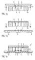
- FIGS. 1 a to 1 cthe stages of assembling a flip-chip module according to the invention, in a schematic cross-sectional view
- FIGS. 2 a to 2 cin each case a section through a flip-chip module according to the invention in the area of a soldering point, wherein during the soldering process different distances have been maintained between the respective substrate and the semiconductor chip
- FIGS. 3 a and 3 bin each case a schematic view from below of a semiconductor chip with contact posts and a spacer
- FIG. 4 aa plan view of a flip-chip module according to the invention
- FIG. 4 bthe flip-chip module of FIG. 4 a in a sectional view along line A-A
- FIGS. 5 a and 5 bin each case a section through a flip-chip module according to the invention in the area of a soldering point.
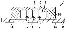
- a flip-chip module 1 according to the invention( FIG. 1 c ) comprises a semiconductor chip 2 with I/O contact points on one side face 3 .
- I/O contact pointsProvided at the I/O contact points are contact posts 4 , each standing upright on the side face 3 .
- the contact posts 4are made of two sections, namely a metal post 5 and a solder section 6 ( FIG. 1 a ).
- the metal post 5is made usually of copper and/or gold, is fitted directly on the semiconductor chip 2 , and is in electrical contact with a conductor path of the semiconductor chip 2 .
- the solder sections 6are located at the ends of the contact posts 4 furthest away from the semiconductor chip 2 , and provide mechanical and electrical connection with contact points 7 of a substrate 8 . So long as the contact posts 4 are not soldered to the contact points 7 of the substrate 8 , the solder sections 6 form free ends of the contact posts 4 ( FIG. 1 a , FIG. 1 b ).
- the contact posts of the present inventionthus comprise an elongated column of an electrically conductive material and a solder section, wherein the column is made of a material which does not melt at the melting temperature of the solder of the solder section.
- the length of the columnis at least 20 ⁇ m, preferably at least 50 ⁇ m, 100 ⁇ m or 200 ⁇ m.
- soldering material of the solder sections 6is for example a tin-lead alloy, or it may also be a lead-free soldering material.
- FIGS. 1 a to 1 chas a contact area 9 in which the contact posts 4 are located and which is formed in the centre of the semiconductor chip 2 .
- three contact postsare shown to simplify the illustration.
- semiconductor chips of a flip-chip module according to the inventionhave between 40 and 200 contact posts. It has been found that, with the flip-chip module according to the invention, semiconductor chips may have more than 100 or more than 200 or more than 500 up to several 1000 directly contactable contact posts on a substrate.
- the centre-to-centre distance between two adjacent contact posts 4is typically 20 ⁇ m to 200 ⁇ m.
- a spacer 10is fitted next to the contact posts 4 , aligned relative to the contact posts 4 and connected to the side face 3 of the semiconductor chip 2 .
- the connection between the spacer 10 and the semiconductor chip 2is made by adhesive bonding, with the spacer 10 being bonded to the semiconductor chip 2 as far as possible over its entire contact surface.
- a soldered connectionmay also be provided. It is not necessary to make the connection over the whole surface. It may also be expedient to connect the spacer 10 to the semiconductor chip 2 at individual points distributed over the contact surfaces.
- connectionwhether made flat or via several connection points, over a contact surface which is at least 10% of the area of the semiconductor chip 2 , and preferably at least 20%, 30%, 50%, 70%, 80% or 90% of the area of the semiconductor chip.
- the spacer 10When the spacer 10 is connected to the semiconductor chip 2 , the latter is still part of a wafer. After the spacer 10 has been connected to the wafer and semiconductor chip 2 respectively, the semiconductor chip is cut out of the wafer by a conventional cutting process (not shown).
- the unit thus obtained, comprising the semiconductor chip 2 and the spacer 10is arranged on the substrate 8 ( FIG. 1 b ) with the free ends of the contact posts 4 or the solder sections 6 on the contact points 7 of the substrate.
- the contact points 7are pretreated copper contacts capable of being soldered.
- the substrate 8 with the spacer element 10 and semiconductor chip 2 placed on topis put into a soldering furnace or a thermal compression facility, in which the whole unit is heated over a temperature profile to a soldering temperature of e.g. 230° C.
- a soldering temperaturee.g. 230° C.
- the soldering material of the solder sections 6is melted, wetting both the lower ends of the metal posts 5 of the semiconductor chip 2 and also the contact points 7 of the substrate 8 .
- On cooling down the soldering materialhardens, thereby providing permanent electrical and mechanical connection of the contact posts 4 of the semiconductor chip 2 with the contact points 7 of the substrate 8 ( FIG. 1 c ).
- the spacer 10is also connected physically to the substrate 8 by means of an adhesive bond or a soldered connection. It is however also possible for the connection between the spacer 10 and the substrate 8 to be made before soldering.
- the connection between the spacer 10 and the substrate 8is expediently made over the whole area of the contact surfaces of the spacer 10 with the substrate 8 .
- the spacer 10Due to the provision of the spacer 10 between the substrate 8 and the semiconductor chip 2 , a predetermined distance between the substrate 8 and the semiconductor chip 2 is maintained during the soldering process.
- the height and thickness respectively of the spaceris determined by means of a measurement of the height of the metal posts after the production process.
- the provision of the spacerimproves the quality of the soldered connection significantly, as explained below with the aid of FIGS. 2 a to 2 c , each of which shows a flip-chip module in the area of a contact post.
- soldered connections of the desired qualityare therefore obtained through the provision of the spacer 10 according to the invention between the substrate 8 and the semiconductor chip 2 .
- the spacer 10it is not necessary for the spacer 10 to be connected physically to the substrate and/or the semiconductor chip 2 , but such a physical connection is preferred, as explained in detail below.
- the spacer 10is made of a rigid material, e.g. fibre-reinforced plastic or a coated steel alloy (Invar®) with a low thermal coefficient of expansion.
- Suitable reinforcing fibres for the fibre-reinforced plasticare carbon fibres and aramid fibres (Kevlar®).
- the spacermay also be made of a semiconductor material such as e.g. silicon.
- the material of the spacerhas a thermal coefficient of expansion which differs less from the thermal coefficient of expansion of the semiconductor chip than from the thermal coefficient of expansion of the substrate. I.e. the thermal expansion of the spacer 10 corresponds more to the semiconductor chip 2 than to the substrate 8 .
- the spacer 10is physically coupled to the substrate 8 , then the thermal stresses between the substrate and the spacer 10 will be absorbed by the spacer 10 and not transmitted to the semiconductor chip 2 .
- the spacer 10has no electrical functional elements and is made of a rigid material, so that the thermal stresses lead to no or at any rate minimal distortions.
- the substrate 8is usually made of a plastic or ceramic material provided with copper conductor paths 12 , and is so stable that it can absorb these mechanical stresses continuously. Although thermal stresses continue to exist between the substrate and the spacer, they do not impair the continuous operation of the flip-chip module according to the invention.
- the unit comprised of the substrate 8 and the spacer 10also forms such a rigid body that no or at any rate only negligible bends are able to occur in the substrate.
- the spacer 10can absorb the thermal stresses generated, it is coupled physically to the substrate 8 .
- This couplingis effected preferably by a flat adhesive bond. In principle, however, it is sufficient for the spacer 10 and the substrate 8 to be connected to one another at several points distributed over their contact surfaces.
- the spacer 10is also possible for the spacer 10 to be coupled physically to the semiconductor chip 2 , with no physical connection between the substrate and the spacer.
- Such a design of the flip-chip module according to the inventionis expedient if it is required that the semiconductor chip 2 should be removable from the substrate 8 for repair work.
- the semiconductor chip 2 and the spacerform a rigid unit, which is much better able to withstand mechanical loads.
- semiconductor chipsare generally coated with a so-called low-k material, which has low strength, it is expedient to make the connection at the contact surface between the spacer and the semiconductor chip over an area corresponding to at least 30%, 50%, 70%, 80%, 90% or 95% of the area of the semiconductor chip.
- a low-k material of this kindis described for example in the INTERNATIONAL TECHNOLOGY ROADMAP FOR SEMICONDUCTORS—INTERCONNECT, 2005 edition, on pages 19 and 20.
- the spacer 10 and the semiconductor chip 2are also connected to one another, at least at several points distributed over their contact surfaces.
- the semiconductor chip 2holds its shape even during the temperature variations occurring in the course of the soldering process, and possible cracking is inhibited.
- the difference between the thermal coefficient of expansion of the spacer and the thermal coefficient of expansion of the semiconductor chipis preferably less than 40% and in particular less than 20% or 10% or 5% of the difference between the thermal coefficient of expansion of the semiconductor chip 2 and the thermal coefficient of expansion of the substrate 8 .
- the spacer 10 according to the inventionwhich is at least physically coupled to the substrate 8 , bends in the flip-chip module according to the invention such as occur in known flip-chip modules are reduced or even completely avoided. As a result, the risk of damage to the soldered connections between the contact posts 4 and the substrate 8 , or of damage to the semiconductor chip 2 is considerably reduced. By this means it is possible to connect electrically and mechanically to a substrate by means of contact posts even semiconductor chips which are sensitive to mechanical stresses, such as e.g. the latest generation of DRAM chips.
- the flip-chip module according to the inventionis suitable for semiconductor chips with up to a thousand contact posts.
- FIG. 3 aThe semiconductor chip 2 shown in FIGS. 1 a and 1 b is illustrated in FIG. 3 a in a view from below together with the spacer 10 . It can be seen that this spacer forms a frame around the contact area 9 in which the contact posts 4 are arranged. This frame is in one piece.
- FIG. 3 bshows an alternative embodiment in which the contact posts 4 are arranged around the edge of the semiconductor chip 2 and a rectangular spacer 10 is provided in the centre.
- FIG. 4 ashows a further embodiment of a flip-chip module 1 according to the invention in a view from above.
- FIG. 4 bshows a section along the line A-A of FIG. 4 a .
- This flip-chip module 1again has a semiconductor chip 2 , a spacer 10 , a substrate 8 and contact posts 4 which are mechanically and electrically connected to the appropriate contact points of the substrate 8 .
- This flip-chip moduleis distinguished by the fact that the spacer 10 protrudes to the side of the semiconductor chip 2 and has a continuous projection 13 oriented upwards, which then encompasses the side edges of the semiconductor chip 2 .
- the projection 13protrudes slightly at the surface of the semiconductor chip, so that the spacer 10 forms a basin in which the semiconductor chip 2 may be cast with a synthetic resin.
- the semiconductor chip 2is protected by the spacer 10 at the side.
- a coverwhich is either bonded directly on to the semiconductor chip 2 , or connected physically to the spacer 10 protruding from the side of the semiconductor chip 2 .
- the spacermay also protrude from the side of the semiconductor chip, without the spacer being formed with an upwards-oriented projection.
- FIG. 5 ashows a section through a flip-chip module according to the invention in the area of a soldering point, with a detail of the semiconductor chip 2 , a contact post 4 , a contact point 7 and a detail of the substrate 8 .
- the contact point 7is provided with a recess 15 to accommodate the lower end of the contact post 4 .
- the recessis a flat circular basin, with a diameter somewhat greater than the diameter of the contact post 4 .
- the contact posts 4 of a semiconductor chip 2are placed in the recesses 15 of the contact points 7 of a substrate 8 . This prevents the semiconductor chip 2 from slipping on the substrate 8 . It is therefore unnecessary, as was the case with conventional methods, to join the semiconductor chip 2 and the substrate 8 temporarily with a large drop of adhesive before soldering. Formerly this drop of adhesive had to extend from the bottom of the semiconductor chip 2 to the top of the substrate 8 and, due to the use of contact posts 4 , had a considerable extent.
- the recesses 15 of the contact points 7simplify the alignment of all contact posts 4 relative to the contact points 7 since, when all lower end sections of the contact posts 4 are located in the relevant recesses 15 , then the contact posts 4 are clearly aligned on the relevant contact point 7 .
- the material of the solder section 6flows into the recess 15 of the respective contact point 7 .
- the recess 15the area in which the material of the solder section 6 is distributed is limited, thus avoiding the risk of fault contacts due to soldering material connecting two contact points 7 with one another.
- the recess 15is formed only in the material of the contact point 7 .
- the recess 15may extend into the substrate 8 .
- the recess extending into the substrate 8is coated by the contact point 7 and forms a deep recess into which a part of the metal post 5 also extends.
- the bottom end section of the metal post 5is encompassed by the material of the solder section 6 , creating on the one hand the electrical connection to the contact point 7 and also a robust mechanical connection. Because of the large connecting surface and the three-dimensional support of the metal post 5 , a soldered connection of high mechanical strength is obtained between the substrate 8 and the semiconductor chip 2 .
- the length of the contact posts 4 relative to the height of the spacer 10is chosen so that an ideal soldered connection results, i.e. in the embodiment according to FIG. 5 a the length of the contact post 4 surrounding the metal post 5 and the solder section 6 does not exceed the height of the spacer 10 , while on the other hand in the embodiment according to FIG. 5 b the length of the contact post 4 is somewhat greater than the height of the spacer 10 .
- the flip-chip module according to the invention explained abovemay be placed on a circuit board as a unit, with the contact points on the circuit board being electrically connected.
- the substrates 8are described as “chip carriers”, having on the surface facing towards the semiconductor chip 2 a grid of contact points 7 in fine pitch and, on the side opposite the semiconductor chip 2 , contact points 14 in a coarser grid. Each contact point 14 is connected electrically to a contact point 7 .
- the contact points 14may be connected electrically and mechanically by conventional soldering methods to contact points provided in a corresponding grid on a circuit board.
- the substrate 8serves as a kind of transmission from a contact point grid in fine pitch to a much coarser contact point grid.
- the flip-chip modules according to the inventionmay also comprise several semiconductor chips, all mounted on a common substrate.
- the flip-chip modules according to the inventionare especially suitable for the production of SIMM modules (Single Inline Memory Modules) and/or DIMM modules (Dual Inline Memory Modules).
- SIMM modulesSingle Inline Memory Modules
- DIMM modulesDual Inline Memory Modules
- Such a flip-chip moduleis provided on the substrate with an edge connector by means of which, through insertion in a corresponding mating edge connector on a circuit board in a computer, it may be contacted by the latter.
- the inventionrelates to a flip-chip module with a semiconductor chip with contact posts, wherein the contact posts are connected electrically and mechanically to a substrate.
- a spacerProvided between the substrate and the semiconductor chip is a spacer, which is coupled mechanically at least to the substrate.
- the inventionalso relates to a method for the production of a flip-chip module, in which firstly a spacer is located between the semiconductor chip and the substrate, after which the contact posts are soldered to the contact points of the substrate. Through the provision of the spacer the distance between the semiconductor chip and the substrate is set precisely, thereby improving the quality of the soldering points.
Landscapes
- Engineering & Computer Science (AREA)
- Computer Hardware Design (AREA)
- Microelectronics & Electronic Packaging (AREA)
- Power Engineering (AREA)
- Physics & Mathematics (AREA)
- Condensed Matter Physics & Semiconductors (AREA)
- General Physics & Mathematics (AREA)
- Wire Bonding (AREA)
- Structures For Mounting Electric Components On Printed Circuit Boards (AREA)
Abstract
Description
- The invention relates to a flip-chip module and a method of producing such a flip-chip module, wherein the flip-chip module comprises a semiconductor chip, which is provided on one face with contact posts, and a substrate with contact points soldered to the free ends of the contact posts.
- Such a flip-chip module is known from U.S. Pat. No. 6,578,754 B1. The contact posts are comprised of one section containing substantially copper, and a shorter section made of the soldering material connected to the contact points of the substrate. The length of the copper section is at least 50 μm. These contact posts are intended for contacting contact points arranged in a regular grid with a grid spacing less than 100 μm and preferably in the range of 80 to 100 μm. Through the provision of defined contact posts, considerable benefits are obtained in comparison with conventional flip-chip modules. In particular, the danger of a short-circuit between adjacent contact points is much less than with conventional flip-chip modules in which the connection between the substrate and the semiconductor chip is made solely by spherical contact elements of soldering material. It is therefore possible for contact points to be contacted reliably in a grid of less than 100 μm.
- Reference is also made to U.S. Pat. No. 6,550,666 B2 and U.S. Pat. No. 6,592,019 B2, in which further embodiments of the flip-chip module with contact posts described above are disclosed.
- This flip-chip module also has all the advantages of conventional flip-chip modules in respect of wire bonding. In particular the path of the electrical circuit between the semiconductor chip and the substrate, and thus the signalling distance, is very short.
- As already described in U.S. Pat. No. 6,578,754 B1 and U.S. Pat. No. 6,592,019 B2, considerable shear stresses may arise between the substrate and the semiconductor chip, which may even lead to distortions in the semiconductor chip and also in the substrate (see e.g. FIG. 4a of U.S. Pat. No. 6,578,754 B1.
- Shear stresses within the flip-chip module are also explained in U.S. Pat. No. 6,592,019 B2. These shear stresses are caused by different thermal coefficients of expansion between the semiconductor chip and the substrate, since in soldering of the contact posts to the substrate, the entire module is placed in a soldering furnace and heated e.g. to around 230° C. At this temperature, the soldering material melts and bonds the contact posts to the relevant contact points of the substrate. The temperature is then reduced, with the soldering material setting at around 200° C. With further lowering of the temperature to room temperature, the substrate shrinks more than the semiconductor chip, leading to distortions in the flip-chip module.
- As a result, in the case of such flip-chip modules with a multiplicity of contact posts, owing to the stresses within the flip-chip module, the soldered connections between the contact posts and the substrate may break up or contact posts may break loose from the semiconductor chip, or the semiconductor chip may even be damaged. It is therefore not possible to provide large semiconductor chips, e.g. DRAM chips, in such a flip-chip module.
- There is however a considerable demand for contacting DRAM chips directly by means of a flip-chip module, without the roundabout route of an additional wiring level, since on the one hand due to the multiplicity of connections conventional contacting by wires is scarcely possible any longer, while on the other hand the desired data transfer rates are not possible with conventional wire bonding.
- The contact points of these DRAM chips are arranged with a grid spacing of less than 100 μm, which is described in the specialist jargon as “fine pitch”. Such fine pitch can be contacted by the contact posts explained above, but conventional contacting methods for flip-chip modules are not suitable for this purpose. It should also be taken into account that for conductor paths within the chip, materials with low dielectricity (low-k passivation materials) are increasingly used. Such materials are mechanically weak, for which reason mechanical stress exerted on such a semiconductor chip leads to cracks and fractures in the passivation layer. Current semiconductor chips are therefore very sensitive to stress, which makes more difficult their use in connection with the flip-chip module described above.
- DE 697 148 T2 shows a connection between a substrate of a flip-chip module and a circuit board, which is in the form of posts of soldering material. The resilience of the soldering material posts compensates for the considerably different thermal coefficients of expansion of the substrate and the circuit board. By using corner contact pins it is possible to increase the contact pressure. The contact pins are made of Kovar and are fixed to the circuit board by brazing.
- Described in U.S. Pat. No. 6,376,915 B1 is a flip-chip module which has a circuit board and a semiconductor chip connected by means of so-called bumps, which both set the distance between the semiconductor chip and the circuit board, and also make an appropriate connection in each case. In the peripheral zone between the circuit board and the semiconductor chip is a continuous wall section made of the same material as the bumps. This wall section is moulded on at the same time as the bumps.
EP 0 930 645 A2 discloses a flip-chip module in which a chip is electrically connected to a circuit board by means of bumps made of metal. The physical connection is made by an adhesive bond of non-conductive adhesive, with which the area between the chip and the circuit board is filled. This adhesive material has a thermal coefficient of expansion which lies between the thermal coefficients of expansion of the chip and the circuit board made of plastic or its plastic holder.- US 2002/0079577 A1 discloses a flip-chip module with a circuit board and a chip, wherein both the chip and the circuit board are provided with soldered connections. The soldered connections in the peripheral area are made of a soldering material with a higher melting temperature, so that only the soldered connections in the inner area melt during the soldering process, and the soldered connections in the peripheral area serve as spacers.
- US 2004/0232561 A1 discloses a flip-chip module in which spacer elements are provided between the chip and the substrate, to ensure adequate height between the chip and the substrate. The spacer elements are so designed that they increase the distance between the chip and the substrate during the soldering process. The electrical connections between the substrate and the chip are formed entirely of soldering material. The intermediate space between the substrate and the chip may be filled out with filler material. This is intended to reduce concentrations of stress at the soldered connections.
- Similar flip-chip modules are disclosed in
GB 2 062 963 A and U.S. Pat. No. 4,878,611. - US 2003/0210531 A1 describes a flip-chip module with a chip and a substrate which are connected by electrically conductive elements, with scope for the insertion of elastic elements in the centre of these electrical connecting elements. Around the chip is a collar, with a gap between the collar and the chip, so that the collar and the chip are not in contact. The collar has a thermal coefficient of expansion and an elasticity similar to those of the chip.
- U.S. Pat. No. 6,046,910 describes a flip-chip module in which a compressible preform of polymer material is fitted between a semiconductor chip and a substrate.
- Other flip-chip modules are disclosed by U.S. Pat. No. 4,647,959 and U.S. Pat. No. 5,834,848.
- The invention is based on the problem of so developing a flip-chip module with the contact posts described above that fewer faults are caused by the strains within the flip-chip module. The invention is also based on the problem of creating a method for the production of such a flip-chip module.
- The problem is solved by a flip-chip module with the features of
claim 1 and by a method with the features of claim16. Advantageous developments of the invention are set out in the respective dependent claims. - The flip-chip module according to the invention comprises
- a semiconductor chip having on one face contact posts arranged roughly at right-angles to this face,
- a substrate with contact points, each connected to a free end of one of the contact posts, wherein the substrate has a different thermal coefficient of expansion to that of the semiconductor chip, and
- a rigid spacer, located between the substrate and the semiconductor chip, and with a thermal coefficient of expansion varying less from the thermal coefficient of expansion of the semiconductor chip than from the thermal coefficient of expansion of the substrate, wherein the spacer is connected either to the substrate and/or to the semiconductor chip at least at several points distributed over its contact faces.
- Since the spacer is connected to the substrate and/or the semiconductor chip, and the thermal coefficient of expansion of the spacer is closer to the thermal coefficient of expansion of the semiconductor chip than to the thermal coefficient of expansion of the substrate, then either the strains occur mainly between the substrate and the spacer, and not between the substrate and the semiconductor chip, or else the semiconductor chip is so strengthened by the connection to the spacer that it can resist the strains which occur. The spacer thus absorbs the strain of the substrate caused by the differing thermal coefficient of expansion. The spacer, which has no electrical functional elements whatsoever, is of stable design, so that this strain is not transmitted to the sensitive semiconductor chip.
- The connection at several points distributed over the contact surfaces may also be realised through a large surface connection, e.g. a soldered connection or an adhesive bond, with the continuous connecting layer extending over the several distributed points.
- The substrate, which is usually made of a plastic or ceramic material provided with copper conductor paths, is stable enough to absorb these mechanical stresses continuously. With a connection between the substrate and the spacer, the unit comprising the substrate and the spacer is considerably more rigid than the substrate alone, so that the strains produce no bends in the substrate or considerably less than with the flip-chip technology used to date. Also the mechanical loading of the soldering points between the contact posts and the substrate is significantly lower than with the flip-chip modules known to date.
- Through the provision of the rigid spacers, the risk of damage to the soldering points between the contact posts and the substrate, and the risk of damage to the semiconductor chip, are significantly reduced.
- Preferably the spacer is connected both to the substrate and to the semiconductor chip at least at several points distributed over their contact surfaces. Due to the physical connection between the semiconductor chip and the spacer, each having a similar thermal coefficient of expansion, the semiconductor chip holds its shape even during temperature variations occurring in the soldering process, and possible stresses are inhibited.
- The differences between the thermal coefficient of expansion of the spacer and the thermal coefficient of expansion of the semiconductor chip are preferably less than 40%, and in particular less than 20% or 10% of the difference between the thermal coefficient of expansion of the semiconductor chip and the thermal coefficient of expansion of the substrate. The greater the agreement between the thermal coefficients of expansion of the semiconductor chip and the spacer, the lower are the forces acting on the semiconductor chip as a result of thermal stress.
- In the method according to the invention for the production of a flip-chip module, a spacer is first of all placed between the semiconductor chip and the substrate, after which the contact posts are soldered to the contact points of the substrate.
- In this way the distance between the substrate and the semiconductor chip is set precisely. This distance should correspond to the average height of all contact posts including their soldering points.
- The inventors of the present invention have established that, in the method known to date, the problem is that the distance between the substrate and the semiconductor chip is either too short or too long. If the distance is too short, then the soldering material is pressed out from the space between the contact post and the corresponding contact point of the substrate, so that only a very thin connecting layer of soldering material remains between the contact post and the contact point. This thin connecting layer is however mechanically weak, so that it can break quickly under strain.
- If the distance between the semiconductor chip and the substrate is too large, then there is a correspondingly large gap between the contact post and the contact point of the substrate. The soldering material is stretched over this gap, leading to reductions at the soldering point. Such reductions are again mechanically weak, and tend to break up under stress loading. This means that mechanically weak soldering points are created between the semiconductor chip and the substrate, both when distances are too large and also when they are too small. These weak points tend to break up under thermal stresses in the flip-chip module.
- Through the method according to the invention, the distance between the semiconductor chip and the substrate is maintained very precisely, thus considerably lowering the risk of creating physically weak soldering points. A flip-chip module produced by the method according to the invention is therefore better able to absorb thermal stresses, and the risk of damage to the flip-chip module is considerably reduced.
- The flip-chip module according to the invention described above is preferably produced by the method according to the invention, with the spacer coupled to the substrate.
- The invention is explained in detail below with the aid of the drawings, which show in.
FIGS. 1 ato1cthe stages of assembling a flip-chip module according to the invention, in a schematic cross-sectional viewFIGS. 2 ato2cin each case a section through a flip-chip module according to the invention in the area of a soldering point, wherein during the soldering process different distances have been maintained between the respective substrate and the semiconductor chipFIGS. 3 aand3bin each case a schematic view from below of a semiconductor chip with contact posts and a spacerFIG. 4 aa plan view of a flip-chip module according to the inventionFIG. 4 bthe flip-chip module ofFIG. 4 ain a sectional view along line A-AFIGS. 5 aand5bin each case a section through a flip-chip module according to the invention in the area of a soldering point.- A flip-
chip module 1 according to the invention (FIG. 1 c) comprises asemiconductor chip 2 with I/O contact points on oneside face 3. Provided at the I/O contact points arecontact posts 4, each standing upright on theside face 3. - These contact posts are produced in accordance with a method as described in U.S. Pat. No. 6,578,754 B1, U.S. Pat. No. 6,550,666 B2 and U.S. Pat. No. 6,592,019 B2 respectively. Reference is therefore made to the contents of these patents in full, and they are incorporated in the present application.
- The contact posts4 are made of two sections, namely a
metal post 5 and a solder section6 (FIG. 1 a). Themetal post 5 is made usually of copper and/or gold, is fitted directly on thesemiconductor chip 2, and is in electrical contact with a conductor path of thesemiconductor chip 2. Thesolder sections 6 are located at the ends of the contact posts4 furthest away from thesemiconductor chip 2, and provide mechanical and electrical connection withcontact points 7 of asubstrate 8. So long as the contact posts4 are not soldered to the contact points7 of thesubstrate 8, thesolder sections 6 form free ends of the contact posts4 (FIG. 1 a,FIG. 1 b). - The contact posts of the present invention thus comprise an elongated column of an electrically conductive material and a solder section, wherein the column is made of a material which does not melt at the melting temperature of the solder of the solder section. The length of the column is at least 20 μm, preferably at least 50 μm, 100 μm or 200 μm.
- The soldering material of the
solder sections 6 is for example a tin-lead alloy, or it may also be a lead-free soldering material. - The embodiment shown in
FIGS. 1 ato1chas acontact area 9 in which the contact posts4 are located and which is formed in the centre of thesemiconductor chip 2. InFIGS. 1 ato1cthree contact posts are shown to simplify the illustration. Typically, semiconductor chips of a flip-chip module according to the invention have between 40 and 200 contact posts. It has been found that, with the flip-chip module according to the invention, semiconductor chips may have more than 100 or more than 200 or more than 500 up to several1000 directly contactable contact posts on a substrate. The centre-to-centre distance between twoadjacent contact posts 4 is typically 20 μm to 200 μm. The contact posts may be arranged in one or more rows along a line running in the centre of the chip (=centre pinning) or in one or more rows along the edges of the semiconductor chip. - In the method shown in
FIGS. 1 ato1cfor producing a flip-chip module according to the invention, in a first step (FIG. 1 a) aspacer 10 is fitted next to the contact posts4, aligned relative to the contact posts4 and connected to theside face 3 of thesemiconductor chip 2. The connection between thespacer 10 and thesemiconductor chip 2 is made by adhesive bonding, with thespacer 10 being bonded to thesemiconductor chip 2 as far as possible over its entire contact surface. Instead of an adhesive bond, a soldered connection may also be provided. It is not necessary to make the connection over the whole surface. It may also be expedient to connect thespacer 10 to thesemiconductor chip 2 at individual points distributed over the contact surfaces. It is however expedient to provide the connection, whether made flat or via several connection points, over a contact surface which is at least 10% of the area of thesemiconductor chip 2, and preferably at least 20%, 30%, 50%, 70%, 80% or 90% of the area of the semiconductor chip. - When the
spacer 10 is connected to thesemiconductor chip 2, the latter is still part of a wafer. After thespacer 10 has been connected to the wafer andsemiconductor chip 2 respectively, the semiconductor chip is cut out of the wafer by a conventional cutting process (not shown). The unit thus obtained, comprising thesemiconductor chip 2 and thespacer 10, is arranged on the substrate8 (FIG. 1 b) with the free ends of the contact posts4 or thesolder sections 6 on the contact points7 of the substrate. - The contact points7 are pretreated copper contacts capable of being soldered. The
substrate 8 with thespacer element 10 andsemiconductor chip 2 placed on top is put into a soldering furnace or a thermal compression facility, in which the whole unit is heated over a temperature profile to a soldering temperature of e.g. 230° C. By this means the soldering material of thesolder sections 6 is melted, wetting both the lower ends of themetal posts 5 of thesemiconductor chip 2 and also the contact points7 of thesubstrate 8. On cooling down the soldering material hardens, thereby providing permanent electrical and mechanical connection of the contact posts4 of thesemiconductor chip 2 with the contact points7 of the substrate8 (FIG. 1 c). - Preferably, at the same time as the soldering, the
spacer 10 is also connected physically to thesubstrate 8 by means of an adhesive bond or a soldered connection. It is however also possible for the connection between thespacer 10 and thesubstrate 8 to be made before soldering. The connection between thespacer 10 and thesubstrate 8 is expediently made over the whole area of the contact surfaces of thespacer 10 with thesubstrate 8. - Due to the provision of the
spacer 10 between thesubstrate 8 and thesemiconductor chip 2, a predetermined distance between thesubstrate 8 and thesemiconductor chip 2 is maintained during the soldering process. The height and thickness respectively of the spacer is determined by means of a measurement of the height of the metal posts after the production process. The provision of the spacer improves the quality of the soldered connection significantly, as explained below with the aid ofFIGS. 2 ato2c, each of which shows a flip-chip module in the area of a contact post. - In
FIG. 2 athe distance between thesemiconductor chip 2 and thesubstrate 8 during the soldering process was too small. Because of this, a significant portion of the soldering material was pressed out of the area between the contact points7 and themetal post 5. Themetal post 5 acts like a punch, pressing the soldering material to the side. As a result, only a thin layer of soldering material remains between thecontact point 7 and themetal post 5. This thin layer is mechanically weak and may easily break up under the stresses described at the start. There is also the risk of soldering material escaping beyond thecontact point 7 and coming into contact with an adjacent copper track, leading to a short-circuit. - If on the other hand the distance between the
semiconductor chip 2 and thesubstrate 8 is too large (FIG. 2 c), then there is a correspondingly large gap between themetal post 5 and thecontact point 7 of thesubstrate 8. The soldering material is stretched over this gap, leading to areduction 11. This reduction is again mechanically weak, tending to break up under a mechanical load. An alloy forms between the soldering material and the copper of the contact post and the substrate respectively. This alloy is to begin with a good electrical conductor and, immediately after production of the flip-chip module it is not possible to determine by electrical tests that such an alloy is present here. However elements of the alloy, on application of an electrical current may separate preferably in the area of the reduction, so that the cross-section of the conductor path is further reduced or the electrical connections may even be broken. The material will also become brittle over time (Kirkendale voids). - If the distance between the
semiconductor chip 2 and thesubstrate 8 is set correctly, a mechanically stable soldered connection is made between thecontact post 4 and thecontact point 7 of the substrate8 (FIG. 2 b). Soldered connections of the desired quality are therefore obtained through the provision of thespacer 10 according to the invention between thesubstrate 8 and thesemiconductor chip 2. For this purpose it is not necessary for thespacer 10 to be connected physically to the substrate and/or thesemiconductor chip 2, but such a physical connection is preferred, as explained in detail below. - The
spacer 10 is made of a rigid material, e.g. fibre-reinforced plastic or a coated steel alloy (Invar®) with a low thermal coefficient of expansion. Suitable reinforcing fibres for the fibre-reinforced plastic are carbon fibres and aramid fibres (Kevlar®). The spacer may also be made of a semiconductor material such as e.g. silicon. - The material of the spacer has a thermal coefficient of expansion which differs less from the thermal coefficient of expansion of the semiconductor chip than from the thermal coefficient of expansion of the substrate. I.e. the thermal expansion of the
spacer 10 corresponds more to thesemiconductor chip 2 than to thesubstrate 8. - If the
spacer 10 is physically coupled to thesubstrate 8, then the thermal stresses between the substrate and thespacer 10 will be absorbed by thespacer 10 and not transmitted to thesemiconductor chip 2. Thespacer 10 has no electrical functional elements and is made of a rigid material, so that the thermal stresses lead to no or at any rate minimal distortions. Thesubstrate 8 is usually made of a plastic or ceramic material provided with copper conductor paths12, and is so stable that it can absorb these mechanical stresses continuously. Although thermal stresses continue to exist between the substrate and the spacer, they do not impair the continuous operation of the flip-chip module according to the invention. - The unit comprised of the
substrate 8 and thespacer 10 also forms such a rigid body that no or at any rate only negligible bends are able to occur in the substrate. - So that the
spacer 10 can absorb the thermal stresses generated, it is coupled physically to thesubstrate 8. This coupling is effected preferably by a flat adhesive bond. In principle, however, it is sufficient for thespacer 10 and thesubstrate 8 to be connected to one another at several points distributed over their contact surfaces. - It is also possible for the
spacer 10 to be coupled physically to thesemiconductor chip 2, with no physical connection between the substrate and the spacer. Such a design of the flip-chip module according to the invention is expedient if it is required that thesemiconductor chip 2 should be removable from thesubstrate 8 for repair work. In this case thesemiconductor chip 2 and the spacer form a rigid unit, which is much better able to withstand mechanical loads. - Since nowadays, outside the connection zone of the contact posts5, semiconductor chips are generally coated with a so-called low-k material, which has low strength, it is expedient to make the connection at the contact surface between the spacer and the semiconductor chip over an area corresponding to at least 30%, 50%, 70%, 80%, 90% or 95% of the area of the semiconductor chip. Through a connection of the spacer to the semiconductor chip over a wide area, high strength of this unit is ensured. A low-k material of this kind is described for example in the INTERNATIONAL TECHNOLOGY ROADMAP FOR SEMICONDUCTORS—INTERCONNECT, 2005 edition, on pages 19 and 20.
- Preferably the
spacer 10 and thesemiconductor chip 2 are also connected to one another, at least at several points distributed over their contact surfaces. Through the physical connection between thesemiconductor chip 2 and thespacer 10, each of which have a similar thermal coefficient of expansion, thesemiconductor chip 2 holds its shape even during the temperature variations occurring in the course of the soldering process, and possible cracking is inhibited. - The difference between the thermal coefficient of expansion of the spacer and the thermal coefficient of expansion of the semiconductor chip is preferably less than 40% and in particular less than 20% or 10% or 5% of the difference between the thermal coefficient of expansion of the
semiconductor chip 2 and the thermal coefficient of expansion of thesubstrate 8. The closer the agreement between the thermal coefficient of expansion of thesemiconductor chip 2 and that of thespacer 10, the lower the forces acting on thesemiconductor chip 2 due to thermal stresses. - This results in typical thermal coefficients of expansion for the spacer which are 10 to 100 times less than those of the substrate, which is for example an epoxy-glass fibre circuit board.
- With the
spacer 10 according to the invention, which is at least physically coupled to thesubstrate 8, bends in the flip-chip module according to the invention such as occur in known flip-chip modules are reduced or even completely avoided. As a result, the risk of damage to the soldered connections between the contact posts4 and thesubstrate 8, or of damage to thesemiconductor chip 2 is considerably reduced. By this means it is possible to connect electrically and mechanically to a substrate by means of contact posts even semiconductor chips which are sensitive to mechanical stresses, such as e.g. the latest generation of DRAM chips. The flip-chip module according to the invention is suitable for semiconductor chips with up to a thousand contact posts. - The
semiconductor chip 2 shown inFIGS. 1 aand1bis illustrated inFIG. 3 ain a view from below together with thespacer 10. It can be seen that this spacer forms a frame around thecontact area 9 in which the contact posts4 are arranged. This frame is in one piece. - Within the scope of the invention it is also possible to make the
spacer 10 of several separate parts, provided on thesemiconductor chip 2 with clearance from or also adjacent to one another.FIG. 3 bshows an alternative embodiment in which the contact posts4 are arranged around the edge of thesemiconductor chip 2 and arectangular spacer 10 is provided in the centre. FIG. 4 ashows a further embodiment of a flip-chip module 1 according to the invention in a view from above.FIG. 4 bshows a section along the line A-A ofFIG. 4 a. This flip-chip module 1 again has asemiconductor chip 2, aspacer 10, asubstrate 8 andcontact posts 4 which are mechanically and electrically connected to the appropriate contact points of thesubstrate 8. This flip-chip module is distinguished by the fact that thespacer 10 protrudes to the side of thesemiconductor chip 2 and has acontinuous projection 13 oriented upwards, which then encompasses the side edges of thesemiconductor chip 2. Preferably, theprojection 13 protrudes slightly at the surface of the semiconductor chip, so that thespacer 10 forms a basin in which thesemiconductor chip 2 may be cast with a synthetic resin. By this means, thesemiconductor chip 2 is protected by thespacer 10 at the side. Within the scope of the invention it is also possible to provide a cover, which is either bonded directly on to thesemiconductor chip 2, or connected physically to thespacer 10 protruding from the side of thesemiconductor chip 2.- In a further variant of the invention, the spacer may also protrude from the side of the semiconductor chip, without the spacer being formed with an upwards-oriented projection.
FIG. 5 ashows a section through a flip-chip module according to the invention in the area of a soldering point, with a detail of thesemiconductor chip 2, acontact post 4, acontact point 7 and a detail of thesubstrate 8.- The
contact point 7 is provided with arecess 15 to accommodate the lower end of thecontact post 4. Viewed from above, the recess is a flat circular basin, with a diameter somewhat greater than the diameter of thecontact post 4. - Before the soldering process, the contact posts4 of a
semiconductor chip 2 are placed in therecesses 15 of the contact points7 of asubstrate 8. This prevents thesemiconductor chip 2 from slipping on thesubstrate 8. It is therefore unnecessary, as was the case with conventional methods, to join thesemiconductor chip 2 and thesubstrate 8 temporarily with a large drop of adhesive before soldering. Formerly this drop of adhesive had to extend from the bottom of thesemiconductor chip 2 to the top of thesubstrate 8 and, due to the use ofcontact posts 4, had a considerable extent. Moreover therecesses 15 of the contact points7 simplify the alignment of allcontact posts 4 relative to the contact points7 since, when all lower end sections of the contact posts4 are located in therelevant recesses 15, then the contact posts4 are clearly aligned on therelevant contact point 7. - During soldering, the material of the
solder section 6 flows into therecess 15 of therespective contact point 7. Through the provision of therecess 15, the area in which the material of thesolder section 6 is distributed is limited, thus avoiding the risk of fault contacts due to soldering material connecting twocontact points 7 with one another. - In the embodiment according to
FIG. 5 a, therecess 15 is formed only in the material of thecontact point 7. According to a further embodiment (FIG. 5 b), therecess 15 may extend into thesubstrate 8. The recess extending into thesubstrate 8 is coated by thecontact point 7 and forms a deep recess into which a part of themetal post 5 also extends. The bottom end section of themetal post 5 is encompassed by the material of thesolder section 6, creating on the one hand the electrical connection to thecontact point 7 and also a robust mechanical connection. Because of the large connecting surface and the three-dimensional support of themetal post 5, a soldered connection of high mechanical strength is obtained between thesubstrate 8 and thesemiconductor chip 2. - In the embodiments of
FIGS. 5 aand5b, the length of the contact posts4 relative to the height of thespacer 10 is chosen so that an ideal soldered connection results, i.e. in the embodiment according toFIG. 5 athe length of thecontact post 4 surrounding themetal post 5 and thesolder section 6 does not exceed the height of thespacer 10, while on the other hand in the embodiment according toFIG. 5 bthe length of thecontact post 4 is somewhat greater than the height of thespacer 10. - The flip-chip module according to the invention explained above may be placed on a circuit board as a unit, with the contact points on the circuit board being electrically connected. When the flip-chip module is used in this way, the
substrates 8 are described as “chip carriers”, having on the surface facing towards the semiconductor chip2 a grid ofcontact points 7 in fine pitch and, on the side opposite thesemiconductor chip 2, contact points14 in a coarser grid. Eachcontact point 14 is connected electrically to acontact point 7. The contact points14 may be connected electrically and mechanically by conventional soldering methods to contact points provided in a corresponding grid on a circuit board. Here thesubstrate 8 serves as a kind of transmission from a contact point grid in fine pitch to a much coarser contact point grid. - The flip-chip modules according to the invention may also comprise several semiconductor chips, all mounted on a common substrate.
- The flip-chip modules according to the invention are especially suitable for the production of SIMM modules (Single Inline Memory Modules) and/or DIMM modules (Dual Inline Memory Modules). Such a flip-chip module is provided on the substrate with an edge connector by means of which, through insertion in a corresponding mating edge connector on a circuit board in a computer, it may be contacted by the latter.
- The invention may be summarised briefly as follows:
- The invention relates to a flip-chip module with a semiconductor chip with contact posts, wherein the contact posts are connected electrically and mechanically to a substrate. Provided between the substrate and the semiconductor chip is a spacer, which is coupled mechanically at least to the substrate. By this means, thermal stresses in the flip-chip module are absorbed by the spacer and kept away from the semiconductor chip.
- The invention also relates to a method for the production of a flip-chip module, in which firstly a spacer is located between the semiconductor chip and the substrate, after which the contact posts are soldered to the contact points of the substrate. Through the provision of the spacer the distance between the semiconductor chip and the substrate is set precisely, thereby improving the quality of the soldering points.
- 1 flip-chip module
- 2 semiconductor chip
- 3 side face
- 4 contact posts
- 5 metal post
- 6 solder section
- 7 contact point
- 8 substrate
- 9 contact area
- 10 spacer
- 11 reduction
- 12 copper conductor path
- 13 projection
- 14 contact point
- 15 recess
Claims (39)
Applications Claiming Priority (7)
| Application Number | Priority Date | Filing Date | Title |
|---|---|---|---|
| DE102005043910ADE102005043910A1 (en) | 2005-09-14 | 2005-09-14 | Flip-chip module comprises a semiconductor chip having contact columns on a surface, a substrate with contact sites joined to the free ends of the contact columns and a rigid spacer arranged between the substrate and chip |
| DE102005043910.1 | 2005-09-14 | ||
| DE102005043910 | 2005-09-14 | ||
| DE102005050150.8 | 2005-10-19 | ||
| DE102005050150 | 2005-10-19 | ||
| DE102005050150 | 2005-10-19 | ||
| PCT/EP2006/008921WO2007031298A1 (en) | 2005-09-14 | 2006-09-13 | Flip-chip module and method for the production thereof |
Publications (2)
| Publication Number | Publication Date |
|---|---|
| US20110001232A1true US20110001232A1 (en) | 2011-01-06 |
| US8026583B2 US8026583B2 (en) | 2011-09-27 |
Family
ID=37441004
Family Applications (1)
| Application Number | Title | Priority Date | Filing Date |
|---|---|---|---|
| US12/065,830Expired - Fee RelatedUS8026583B2 (en) | 2005-09-14 | 2006-09-13 | Flip-chip module and method for the production thereof |
Country Status (4)
| Country | Link |
|---|---|
| US (1) | US8026583B2 (en) |
| KR (1) | KR101247138B1 (en) |
| DE (1) | DE112006002428A5 (en) |
| WO (1) | WO2007031298A1 (en) |
Cited By (3)
| Publication number | Priority date | Publication date | Assignee | Title |
|---|---|---|---|---|
| CN113013136A (en)* | 2021-02-25 | 2021-06-22 | 日月光半导体制造股份有限公司 | Semiconductor package device and method of manufacturing the same |
| US11398423B2 (en)* | 2018-03-29 | 2022-07-26 | Siemens Aktiengesellschaft | Semiconductor assembly and method of producing the semiconductor assembly |
| EP4270479A4 (en)* | 2021-01-28 | 2024-07-10 | Huawei Technologies Co., Ltd. | INTERCONNECTION ARRANGEMENT, PLATE LEVEL ARCHITECTURE AND COMPUTER DEVICE |
Families Citing this family (2)
| Publication number | Priority date | Publication date | Assignee | Title |
|---|---|---|---|---|
| DE102006006561B4 (en) | 2006-02-13 | 2009-03-05 | Htc Beteiligungs Gmbh | Flip-chip module and method for exchanging a semiconductor chip of a flip-chip module |
| US9761542B1 (en) | 2016-09-07 | 2017-09-12 | International Business Machines Corporation | Liquid metal flip chip devices |
Citations (45)
| Publication number | Priority date | Publication date | Assignee | Title |
|---|---|---|---|---|
| US4647959A (en)* | 1985-05-20 | 1987-03-03 | Tektronix, Inc. | Integrated circuit package, and method of forming an integrated circuit package |
| US4878611A (en)* | 1986-05-30 | 1989-11-07 | American Telephone And Telegraph Company, At&T Bell Laboratories | Process for controlling solder joint geometry when surface mounting a leadless integrated circuit package on a substrate |
| US5219117A (en)* | 1991-11-01 | 1993-06-15 | Motorola, Inc. | Method of transferring solder balls onto a semiconductor device |
| US5379191A (en)* | 1991-02-26 | 1995-01-03 | Microelectronics And Computer Technology Corporation | Compact adapter package providing peripheral to area translation for an integrated circuit chip |
| US5478778A (en)* | 1991-08-30 | 1995-12-26 | Nec Corporation | Method of manufacturing a compact optical semiconductor module capable of being readily assembled with a high precision |
| US5556293A (en)* | 1994-06-10 | 1996-09-17 | Pfaff; Wayne K. | Mounting apparatus for ball grid array device |
| US5684677A (en)* | 1993-06-24 | 1997-11-04 | Kabushiki Kaisha Toshiba | Electronic circuit device |
| US5818107A (en)* | 1997-01-17 | 1998-10-06 | International Business Machines Corporation | Chip stacking by edge metallization |
| US5834848A (en)* | 1996-12-03 | 1998-11-10 | Kabushiki Kaisha Toshiba | Electronic device and semiconductor package |
| US5872051A (en)* | 1995-08-02 | 1999-02-16 | International Business Machines Corporation | Process for transferring material to semiconductor chip conductive pads using a transfer substrate |
| US5951305A (en)* | 1998-07-09 | 1999-09-14 | Tessera, Inc. | Lidless socket and method of making same |
| US6046910A (en)* | 1998-03-18 | 2000-04-04 | Motorola, Inc. | Microelectronic assembly having slidable contacts and method for manufacturing the assembly |
| US6140144A (en)* | 1996-08-08 | 2000-10-31 | Integrated Sensing Systems, Inc. | Method for packaging microsensors |
| US6159770A (en)* | 1995-11-08 | 2000-12-12 | Fujitsu Limited | Method and apparatus for fabricating semiconductor device |
| US6326241B1 (en)* | 1997-12-29 | 2001-12-04 | Visteon Global Technologies, Inc. | Solderless flip-chip assembly and method and material for same |
| US6329711B1 (en)* | 1995-11-08 | 2001-12-11 | Fujitsu Limited | Semiconductor device and mounting structure |
| US6376915B1 (en)* | 1999-02-26 | 2002-04-23 | Rohm Co., Ltd | Semiconductor device and semiconductor chip |
| US6395991B1 (en)* | 1996-07-29 | 2002-05-28 | International Business Machines Corporation | Column grid array substrate attachment with heat sink stress relief |
| US20020079577A1 (en)* | 1999-12-03 | 2002-06-27 | Ho Tony H. | Advanced electronic package |
| US6428328B2 (en)* | 1998-01-09 | 2002-08-06 | Tessera, Inc. | Method of making a connection to a microelectronic element |
| US6454159B1 (en)* | 1999-08-18 | 2002-09-24 | International Business Machines Corporation | Method for forming electrical connecting structure |
| US20020180029A1 (en)* | 2001-04-25 | 2002-12-05 | Hideki Higashitani | Semiconductor device with intermediate connector |
| US20030017654A1 (en)* | 2001-07-19 | 2003-01-23 | Naofumi Iwamoto | Semiconductor chip having a supporting member, tape substrate, semiconductor package having the semiconductor chip and the tape substrate, and the method of manufacturing the same |
| US6550666B2 (en)* | 2001-08-21 | 2003-04-22 | Advanpack Solutions Pte Ltd | Method for forming a flip chip on leadframe semiconductor package |
| US6578754B1 (en)* | 2000-04-27 | 2003-06-17 | Advanpack Solutions Pte. Ltd. | Pillar connections for semiconductor chips and method of manufacture |
| US6592019B2 (en)* | 2000-04-27 | 2003-07-15 | Advanpack Solutions Pte. Ltd | Pillar connections for semiconductor chips and method of manufacture |
| US20030170921A1 (en)* | 2000-06-08 | 2003-09-11 | Salman Akram | Methods for forming semiconductor devices so as to stabilize the same when positioned face-down over test substrates |
| US6624512B2 (en)* | 2001-12-18 | 2003-09-23 | Mitsubishi Denki Kabushiki Kaisha | Semiconductor integrated circuit device and printed wired board for mounting the same |
| US20030210531A1 (en)* | 2001-03-22 | 2003-11-13 | Alcoe David J. | Method of forming an apparatus to reduce thermal fatigue stress on flip chip solder connections |
| US6649444B2 (en)* | 2000-06-08 | 2003-11-18 | Micron Technology, Inc. | Stereolithographic method and apparatus for fabricating spacers for semiconductor devices and resulting structures |
| US6677677B2 (en)* | 2001-09-25 | 2004-01-13 | Mitsubishi Denki Kabushiki Kaisha | Semiconductor device |
| US6710455B2 (en)* | 2001-08-30 | 2004-03-23 | Infineon Technologies Ag | Electronic component with at least two stacked semiconductor chips and method for fabricating the electronic component |
| US20040130034A1 (en)* | 2001-06-13 | 2004-07-08 | Advanpack Solutions Pte Ltd. | Method for forming a wafer level chip scale package |
| US20040189143A1 (en)* | 2003-03-13 | 2004-09-30 | Olympus Corporation | Electrostatic driving device and manufacturing method of the same |
| US20040232561A1 (en)* | 2003-05-22 | 2004-11-25 | Texas Instruments Incorporated | System and method to increase die stand-off height |
| US6906425B2 (en)* | 2002-03-05 | 2005-06-14 | Resolution Performance Products Llc | Attachment of surface mount devices to printed circuit boards using a thermoplastic adhesive |
| US6917525B2 (en)* | 2001-11-27 | 2005-07-12 | Nanonexus, Inc. | Construction structures and manufacturing processes for probe card assemblies and packages having wafer level springs |
| US6959489B2 (en)* | 2000-09-29 | 2005-11-01 | Tessera, Inc. | Methods of making microelectronic packages |
| US6969635B2 (en)* | 2000-12-07 | 2005-11-29 | Reflectivity, Inc. | Methods for depositing, releasing and packaging micro-electromechanical devices on wafer substrates |
| US7161237B2 (en)* | 2002-03-04 | 2007-01-09 | Micron Technology, Inc. | Flip chip packaging using recessed interposer terminals |
| US7192796B2 (en)* | 2003-07-03 | 2007-03-20 | Tessera Technologies Hungary Kft. | Methods and apparatus for packaging integrated circuit devices |
| US7253516B2 (en)* | 2003-10-10 | 2007-08-07 | Nxp B.V. | Electronic device and carrier substrate for same |
| US7311531B2 (en)* | 2003-03-26 | 2007-12-25 | Jsr Corporation | Anisotropic conductive connector, conductive paste composition, probe member, wafer inspection device and wafer inspection method |
| US20090224851A1 (en)* | 2005-06-07 | 2009-09-10 | Epcos Ag | Electrical component and production method |
| US7667323B2 (en)* | 2004-11-12 | 2010-02-23 | Analog Devices, Inc. | Spaced, bumped component structure |
Family Cites Families (3)
| Publication number | Priority date | Publication date | Assignee | Title |
|---|---|---|---|---|
| JPS5678356U (en) | 1979-11-12 | 1981-06-25 | ||
| JP4577980B2 (en)* | 2000-12-13 | 2010-11-10 | 京セラ株式会社 | Mounting board |
| JP3782753B2 (en)* | 2001-04-25 | 2006-06-07 | 松下電器産業株式会社 | Semiconductor device manufacturing method and semiconductor device |
- 2006
- 2006-09-13DEDE112006002428Tpatent/DE112006002428A5/ennot_activeWithdrawn
- 2006-09-13USUS12/065,830patent/US8026583B2/ennot_activeExpired - Fee Related
- 2006-09-13KRKR1020087008808Apatent/KR101247138B1/ennot_activeExpired - Fee Related
- 2006-09-13WOPCT/EP2006/008921patent/WO2007031298A1/enactiveApplication Filing
Patent Citations (48)
| Publication number | Priority date | Publication date | Assignee | Title |
|---|---|---|---|---|
| US4647959A (en)* | 1985-05-20 | 1987-03-03 | Tektronix, Inc. | Integrated circuit package, and method of forming an integrated circuit package |
| US4878611A (en)* | 1986-05-30 | 1989-11-07 | American Telephone And Telegraph Company, At&T Bell Laboratories | Process for controlling solder joint geometry when surface mounting a leadless integrated circuit package on a substrate |
| US5379191A (en)* | 1991-02-26 | 1995-01-03 | Microelectronics And Computer Technology Corporation | Compact adapter package providing peripheral to area translation for an integrated circuit chip |
| US5478778A (en)* | 1991-08-30 | 1995-12-26 | Nec Corporation | Method of manufacturing a compact optical semiconductor module capable of being readily assembled with a high precision |
| US5219117A (en)* | 1991-11-01 | 1993-06-15 | Motorola, Inc. | Method of transferring solder balls onto a semiconductor device |
| US5684677A (en)* | 1993-06-24 | 1997-11-04 | Kabushiki Kaisha Toshiba | Electronic circuit device |
| US5556293A (en)* | 1994-06-10 | 1996-09-17 | Pfaff; Wayne K. | Mounting apparatus for ball grid array device |
| US5872051A (en)* | 1995-08-02 | 1999-02-16 | International Business Machines Corporation | Process for transferring material to semiconductor chip conductive pads using a transfer substrate |
| US6329711B1 (en)* | 1995-11-08 | 2001-12-11 | Fujitsu Limited | Semiconductor device and mounting structure |
| US6159770A (en)* | 1995-11-08 | 2000-12-12 | Fujitsu Limited | Method and apparatus for fabricating semiconductor device |
| US6395991B1 (en)* | 1996-07-29 | 2002-05-28 | International Business Machines Corporation | Column grid array substrate attachment with heat sink stress relief |
| US6140144A (en)* | 1996-08-08 | 2000-10-31 | Integrated Sensing Systems, Inc. | Method for packaging microsensors |
| US5834848A (en)* | 1996-12-03 | 1998-11-10 | Kabushiki Kaisha Toshiba | Electronic device and semiconductor package |
| US5818107A (en)* | 1997-01-17 | 1998-10-06 | International Business Machines Corporation | Chip stacking by edge metallization |
| US6326241B1 (en)* | 1997-12-29 | 2001-12-04 | Visteon Global Technologies, Inc. | Solderless flip-chip assembly and method and material for same |
| US6428328B2 (en)* | 1998-01-09 | 2002-08-06 | Tessera, Inc. | Method of making a connection to a microelectronic element |
| US6046910A (en)* | 1998-03-18 | 2000-04-04 | Motorola, Inc. | Microelectronic assembly having slidable contacts and method for manufacturing the assembly |
| US5951305A (en)* | 1998-07-09 | 1999-09-14 | Tessera, Inc. | Lidless socket and method of making same |
| US6376915B1 (en)* | 1999-02-26 | 2002-04-23 | Rohm Co., Ltd | Semiconductor device and semiconductor chip |
| US6454159B1 (en)* | 1999-08-18 | 2002-09-24 | International Business Machines Corporation | Method for forming electrical connecting structure |
| US20020079577A1 (en)* | 1999-12-03 | 2002-06-27 | Ho Tony H. | Advanced electronic package |
| US6578754B1 (en)* | 2000-04-27 | 2003-06-17 | Advanpack Solutions Pte. Ltd. | Pillar connections for semiconductor chips and method of manufacture |
| US6592019B2 (en)* | 2000-04-27 | 2003-07-15 | Advanpack Solutions Pte. Ltd | Pillar connections for semiconductor chips and method of manufacture |
| US6649444B2 (en)* | 2000-06-08 | 2003-11-18 | Micron Technology, Inc. | Stereolithographic method and apparatus for fabricating spacers for semiconductor devices and resulting structures |
| US7041513B2 (en)* | 2000-06-08 | 2006-05-09 | Micron Technology, Inc. | Methods for forming semiconductor devices so as to stabilize the same when positioned face-down over test substrates |
| US20030170921A1 (en)* | 2000-06-08 | 2003-09-11 | Salman Akram | Methods for forming semiconductor devices so as to stabilize the same when positioned face-down over test substrates |
| US6959489B2 (en)* | 2000-09-29 | 2005-11-01 | Tessera, Inc. | Methods of making microelectronic packages |
| US6969635B2 (en)* | 2000-12-07 | 2005-11-29 | Reflectivity, Inc. | Methods for depositing, releasing and packaging micro-electromechanical devices on wafer substrates |
| US20030210531A1 (en)* | 2001-03-22 | 2003-11-13 | Alcoe David J. | Method of forming an apparatus to reduce thermal fatigue stress on flip chip solder connections |
| US7247508B2 (en)* | 2001-04-25 | 2007-07-24 | Matsushita Electric Industrial Co., Ltd. | Semiconductor device with intermediate connector |
| US20020180029A1 (en)* | 2001-04-25 | 2002-12-05 | Hideki Higashitani | Semiconductor device with intermediate connector |
| US20040130034A1 (en)* | 2001-06-13 | 2004-07-08 | Advanpack Solutions Pte Ltd. | Method for forming a wafer level chip scale package |
| US20030017654A1 (en)* | 2001-07-19 | 2003-01-23 | Naofumi Iwamoto | Semiconductor chip having a supporting member, tape substrate, semiconductor package having the semiconductor chip and the tape substrate, and the method of manufacturing the same |
| US6683369B2 (en)* | 2001-07-19 | 2004-01-27 | Oki Electric Industry Co., Ltd. | Semiconductor chip having a supporting member, tape substrate, semiconductor package having the semiconductor chip and the tape substrate |
| US6550666B2 (en)* | 2001-08-21 | 2003-04-22 | Advanpack Solutions Pte Ltd | Method for forming a flip chip on leadframe semiconductor package |
| US6710455B2 (en)* | 2001-08-30 | 2004-03-23 | Infineon Technologies Ag | Electronic component with at least two stacked semiconductor chips and method for fabricating the electronic component |
| US6677677B2 (en)* | 2001-09-25 | 2004-01-13 | Mitsubishi Denki Kabushiki Kaisha | Semiconductor device |
| US6917525B2 (en)* | 2001-11-27 | 2005-07-12 | Nanonexus, Inc. | Construction structures and manufacturing processes for probe card assemblies and packages having wafer level springs |
| US6624512B2 (en)* | 2001-12-18 | 2003-09-23 | Mitsubishi Denki Kabushiki Kaisha | Semiconductor integrated circuit device and printed wired board for mounting the same |
| US7161237B2 (en)* | 2002-03-04 | 2007-01-09 | Micron Technology, Inc. | Flip chip packaging using recessed interposer terminals |
| US6906425B2 (en)* | 2002-03-05 | 2005-06-14 | Resolution Performance Products Llc | Attachment of surface mount devices to printed circuit boards using a thermoplastic adhesive |
| US20040189143A1 (en)* | 2003-03-13 | 2004-09-30 | Olympus Corporation | Electrostatic driving device and manufacturing method of the same |
| US7311531B2 (en)* | 2003-03-26 | 2007-12-25 | Jsr Corporation | Anisotropic conductive connector, conductive paste composition, probe member, wafer inspection device and wafer inspection method |
| US20040232561A1 (en)* | 2003-05-22 | 2004-11-25 | Texas Instruments Incorporated | System and method to increase die stand-off height |
| US7192796B2 (en)* | 2003-07-03 | 2007-03-20 | Tessera Technologies Hungary Kft. | Methods and apparatus for packaging integrated circuit devices |
| US7253516B2 (en)* | 2003-10-10 | 2007-08-07 | Nxp B.V. | Electronic device and carrier substrate for same |
| US7667323B2 (en)* | 2004-11-12 | 2010-02-23 | Analog Devices, Inc. | Spaced, bumped component structure |
| US20090224851A1 (en)* | 2005-06-07 | 2009-09-10 | Epcos Ag | Electrical component and production method |
Cited By (4)
| Publication number | Priority date | Publication date | Assignee | Title |
|---|---|---|---|---|
| US11398423B2 (en)* | 2018-03-29 | 2022-07-26 | Siemens Aktiengesellschaft | Semiconductor assembly and method of producing the semiconductor assembly |
| EP4270479A4 (en)* | 2021-01-28 | 2024-07-10 | Huawei Technologies Co., Ltd. | INTERCONNECTION ARRANGEMENT, PLATE LEVEL ARCHITECTURE AND COMPUTER DEVICE |
| US12418985B2 (en) | 2021-01-28 | 2025-09-16 | Huawei Technologies Co., Ltd. | Connection assembly, board-level architecture, and computing device |
| CN113013136A (en)* | 2021-02-25 | 2021-06-22 | 日月光半导体制造股份有限公司 | Semiconductor package device and method of manufacturing the same |
Also Published As
| Publication number | Publication date |
|---|---|
| WO2007031298A8 (en) | 2007-09-20 |
| KR20080056726A (en) | 2008-06-23 |
| DE112006002428A5 (en) | 2008-12-11 |
| KR101247138B1 (en) | 2013-03-29 |
| US8026583B2 (en) | 2011-09-27 |
| WO2007031298A1 (en) | 2007-03-22 |
Similar Documents
| Publication | Publication Date | Title |
|---|---|---|
| US6458623B1 (en) | Conductive adhesive interconnection with insulating polymer carrier | |
| USRE43607E1 (en) | Method and apparatus for evaluating a known good die using both wire bond and flip-chip interconnects | |
| KR100272154B1 (en) | Semiconductor device and manufacturing method thereof | |
| JP2533511B2 (en) | Electronic component connection structure and manufacturing method thereof | |
| JP5212118B2 (en) | Semiconductor device and manufacturing method thereof | |
| US20030052156A1 (en) | Hollow solder structure having improved reliability and method of manufacturing same | |
| KR101376264B1 (en) | Stacked package and method for manufacturing the package | |
| CN101026139A (en) | Semiconductor integrated circuit device | |
| KR20080030897A (en) | Semiconductor devices, semiconductor packages, and manufacturing methods thereof | |
| US8026583B2 (en) | Flip-chip module and method for the production thereof | |
| US6272741B1 (en) | Hybrid solder ball and pin grid array circuit board interconnect system and method | |
| US20150235965A1 (en) | Semiconductor device manufacturing method | |
| JP4768384B2 (en) | Optical transmission line holding member and optical module | |
| US7042088B2 (en) | Package structure with two solder arrays | |
| US6400034B1 (en) | Semiconductor device | |
| US6893890B2 (en) | Method of producing a light-emitting diode | |
| CN100472770C (en) | Area array package with solder balls not electrically connected | |
| US8143715B2 (en) | Semiconductor package transformer | |
| US20150200176A1 (en) | Semiconductor device and method for producing same | |
| US20020079124A1 (en) | Stress relieving tape bonding interconnect | |
| US6803647B2 (en) | Mounting structure of semiconductor device and mounting method thereof | |
| JP3168987B2 (en) | Mounting structure of surface mount type semiconductor device | |
| JPH08139226A (en) | Semiconductor circuit device and method for mounting its circuit | |
| US20030114028A1 (en) | Solder-bearing lead | |
| US20150262957A1 (en) | Semiconductor package |
Legal Events
| Date | Code | Title | Description |
|---|---|---|---|
| AS | Assignment | Owner name:HTC BETEILIGUNGS GMBH, GERMANY Free format text:ASSIGNMENT OF ASSIGNORS INTEREST;ASSIGNOR:WEISSBACH, ERNST-A.;REEL/FRAME:021987/0761 Effective date:20081204 | |
| AS | Assignment | Owner name:HTC BETEILIGUNGS GMBH, GERMANY Free format text:ASSIGNMENT OF ASSIGNORS INTEREST;ASSIGNOR:ERTL, JUERGEN;REEL/FRAME:025340/0008 Effective date:20070131 | |
| STCF | Information on status: patent grant | Free format text:PATENTED CASE | |
| FEPP | Fee payment procedure | Free format text:PAT HOLDER NO LONGER CLAIMS SMALL ENTITY STATUS, ENTITY STATUS SET TO UNDISCOUNTED (ORIGINAL EVENT CODE: STOL); ENTITY STATUS OF PATENT OWNER: LARGE ENTITY | |
| FPAY | Fee payment | Year of fee payment:4 | |
| AS | Assignment | Owner name:RPX CORPORATION, CALIFORNIA Free format text:ASSIGNMENT OF ASSIGNORS INTEREST;ASSIGNOR:HTC BETEILIGUNGS GMBH;REEL/FRAME:035279/0362 Effective date:20150326 | |
| AS | Assignment | Owner name:JPMORGAN CHASE BANK, N.A., AS COLLATERAL AGENT, IL Free format text:SECURITY AGREEMENT;ASSIGNORS:RPX CORPORATION;RPX CLEARINGHOUSE LLC;REEL/FRAME:038041/0001 Effective date:20160226 | |
| AS | Assignment | Owner name:RPX CLEARINGHOUSE LLC, CALIFORNIA Free format text:RELEASE (REEL 038041 / FRAME 0001);ASSIGNOR:JPMORGAN CHASE BANK, N.A.;REEL/FRAME:044970/0030 Effective date:20171222 Owner name:RPX CORPORATION, CALIFORNIA Free format text:RELEASE (REEL 038041 / FRAME 0001);ASSIGNOR:JPMORGAN CHASE BANK, N.A.;REEL/FRAME:044970/0030 Effective date:20171222 | |
| AS | Assignment | Owner name:JEFFERIES FINANCE LLC, NEW YORK Free format text:SECURITY INTEREST;ASSIGNOR:RPX CORPORATION;REEL/FRAME:046486/0433 Effective date:20180619 | |
| FEPP | Fee payment procedure | Free format text:MAINTENANCE FEE REMINDER MAILED (ORIGINAL EVENT CODE: REM.); ENTITY STATUS OF PATENT OWNER: LARGE ENTITY | |
| LAPS | Lapse for failure to pay maintenance fees | Free format text:PATENT EXPIRED FOR FAILURE TO PAY MAINTENANCE FEES (ORIGINAL EVENT CODE: EXP.); ENTITY STATUS OF PATENT OWNER: LARGE ENTITY | |
| STCH | Information on status: patent discontinuation | Free format text:PATENT EXPIRED DUE TO NONPAYMENT OF MAINTENANCE FEES UNDER 37 CFR 1.362 | |
| FP | Lapsed due to failure to pay maintenance fee | Effective date:20190927 | |
| AS | Assignment | Owner name:RPX CORPORATION, CALIFORNIA Free format text:RELEASE BY SECURED PARTY;ASSIGNOR:JEFFERIES FINANCE LLC;REEL/FRAME:054486/0422 Effective date:20201023 |