US20110001116A1 - Back to back resistive random access memory cells - Google Patents
Back to back resistive random access memory cellsDownload PDFInfo
- Publication number
- US20110001116A1 US20110001116A1US12/829,305US82930510AUS2011001116A1US 20110001116 A1US20110001116 A1US 20110001116A1US 82930510 AUS82930510 AUS 82930510AUS 2011001116 A1US2011001116 A1US 2011001116A1
- Authority
- US
- United States
- Prior art keywords
- layer
- rram
- devices
- metal
- formed over
- Prior art date
- Legal status (The legal status is an assumption and is not a legal conclusion. Google has not performed a legal analysis and makes no representation as to the accuracy of the status listed.)
- Granted
Links
- 229910052751metalInorganic materials0.000claimsabstractdescription118
- 239000002184metalSubstances0.000claimsabstractdescription118
- 230000004888barrier functionEffects0.000claimsabstractdescription72
- 239000004065semiconductorSubstances0.000claimsabstractdescription6
- 239000000758substrateSubstances0.000claimsabstractdescription6
- 229910021420polycrystalline siliconInorganic materials0.000claimsdescription12
- 229920005591polysiliconPolymers0.000claimsdescription12
- 239000010410layerSubstances0.000abstractdescription199
- 239000011229interlayerSubstances0.000abstractdescription14
- 238000005498polishingMethods0.000abstractdescription3
- 239000010949copperSubstances0.000description71
- RYGMFSIKBFXOCR-UHFFFAOYSA-NCopperChemical compound[Cu]RYGMFSIKBFXOCR-UHFFFAOYSA-N0.000description68
- 229910052802copperInorganic materials0.000description51
- 230000015654memoryEffects0.000description41
- 239000000872bufferSubstances0.000description40
- 239000000463materialSubstances0.000description36
- 238000010586diagramMethods0.000description29
- 150000002500ionsChemical class0.000description23
- 238000000034methodMethods0.000description22
- 238000009792diffusion processMethods0.000description20
- 238000005516engineering processMethods0.000description16
- 239000007784solid electrolyteSubstances0.000description15
- 230000008569processEffects0.000description14
- ATJFFYVFTNAWJD-UHFFFAOYSA-NTinChemical compound[Sn]ATJFFYVFTNAWJD-UHFFFAOYSA-N0.000description11
- 229910052718tinInorganic materials0.000description11
- 238000001465metallisationMethods0.000description10
- 230000008901benefitEffects0.000description8
- 150000004770chalcogenidesChemical class0.000description7
- 239000011521glassSubstances0.000description7
- 230000014759maintenance of locationEffects0.000description7
- 230000000295complement effectEffects0.000description6
- 238000013461designMethods0.000description6
- 230000006870functionEffects0.000description6
- 230000003068static effectEffects0.000description6
- 229910052721tungstenInorganic materials0.000description6
- 238000000151depositionMethods0.000description5
- 238000004519manufacturing processMethods0.000description5
- 238000003860storageMethods0.000description5
- WFKWXMTUELFFGS-UHFFFAOYSA-NtungstenChemical compound[W]WFKWXMTUELFFGS-UHFFFAOYSA-N0.000description5
- 239000010937tungstenSubstances0.000description5
- 230000008859changeEffects0.000description4
- 239000004020conductorSubstances0.000description4
- 239000004744fabricSubstances0.000description4
- 238000007667floatingMethods0.000description4
- 230000003071parasitic effectEffects0.000description4
- VYPSYNLAJGMNEJ-UHFFFAOYSA-NSilicium dioxideChemical groupO=[Si]=OVYPSYNLAJGMNEJ-UHFFFAOYSA-N0.000description3
- 230000008878couplingEffects0.000description3
- 238000010168coupling processMethods0.000description3
- 238000005859coupling reactionMethods0.000description3
- 239000003989dielectric materialSubstances0.000description3
- 230000000670limiting effectEffects0.000description3
- 239000011295pitchSubstances0.000description3
- 230000002441reversible effectEffects0.000description3
- PXHVJJICTQNCMI-UHFFFAOYSA-NNickelChemical compound[Ni]PXHVJJICTQNCMI-UHFFFAOYSA-N0.000description2
- 230000009286beneficial effectEffects0.000description2
- 238000011109contaminationMethods0.000description2
- 230000008021depositionEffects0.000description2
- 238000011161developmentMethods0.000description2
- 239000000945fillerSubstances0.000description2
- 239000000047productSubstances0.000description2
- 230000005855radiationEffects0.000description2
- 229910052709silverInorganic materials0.000description2
- 230000007704transitionEffects0.000description2
- 102100031102C-C motif chemokine 4Human genes0.000description1
- 101100054773Caenorhabditis elegans act-2 geneProteins0.000description1
- QPLDLSVMHZLSFG-UHFFFAOYSA-NCopper oxideChemical compound[Cu]=OQPLDLSVMHZLSFG-UHFFFAOYSA-N0.000description1
- 239000005751Copper oxideSubstances0.000description1
- 102100026816DNA-dependent metalloprotease SPRTNHuman genes0.000description1
- 101710175461DNA-dependent metalloprotease SPRTNProteins0.000description1
- 229910005900GeTeInorganic materials0.000description1
- XUIMIQQOPSSXEZ-UHFFFAOYSA-NSiliconChemical compound[Si]XUIMIQQOPSSXEZ-UHFFFAOYSA-N0.000description1
- BQCADISMDOOEFD-UHFFFAOYSA-NSilverChemical compound[Ag]BQCADISMDOOEFD-UHFFFAOYSA-N0.000description1
- 229910004166TaNInorganic materials0.000description1
- 229910021417amorphous siliconInorganic materials0.000description1
- 238000013459approachMethods0.000description1
- 238000003491arrayMethods0.000description1
- 230000003139buffering effectEffects0.000description1
- 230000015556catabolic processEffects0.000description1
- 229910052681coesiteInorganic materials0.000description1
- 239000000356contaminantSubstances0.000description1
- 229910000431copper oxideInorganic materials0.000description1
- 229910052906cristobaliteInorganic materials0.000description1
- 230000007547defectEffects0.000description1
- 230000009977dual effectEffects0.000description1
- 239000002355dual-layerSubstances0.000description1
- 230000000694effectsEffects0.000description1
- 230000005684electric fieldEffects0.000description1
- 238000005530etchingMethods0.000description1
- 230000004927fusionEffects0.000description1
- 230000006872improvementEffects0.000description1
- 230000002427irreversible effectEffects0.000description1
- 230000000873masking effectEffects0.000description1
- 239000011159matrix materialSubstances0.000description1
- 230000007246mechanismEffects0.000description1
- 229910044991metal oxideInorganic materials0.000description1
- 150000004706metal oxidesChemical class0.000description1
- 150000002739metalsChemical class0.000description1
- 238000012986modificationMethods0.000description1
- 230000004048modificationEffects0.000description1
- 229910052759nickelInorganic materials0.000description1
- 239000012811non-conductive materialSubstances0.000description1
- 230000036961partial effectEffects0.000description1
- 238000012545processingMethods0.000description1
- 238000009877renderingMethods0.000description1
- 230000000284resting effectEffects0.000description1
- 239000000565sealantSubstances0.000description1
- 238000000926separation methodMethods0.000description1
- 229910052710siliconInorganic materials0.000description1
- 239000010703siliconSubstances0.000description1
- 239000000377silicon dioxideSubstances0.000description1
- 235000012239silicon dioxideNutrition0.000description1
- 229910052814silicon oxideInorganic materials0.000description1
- 239000004332silverSubstances0.000description1
- 229910052682stishoviteInorganic materials0.000description1
- 239000013589supplementSubstances0.000description1
- 230000001360synchronised effectEffects0.000description1
- 229910052715tantalumInorganic materials0.000description1
- PBCFLUZVCVVTBY-UHFFFAOYSA-Ntantalum pentoxideInorganic materialsO=[Ta](=O)O[Ta](=O)=OPBCFLUZVCVVTBY-UHFFFAOYSA-N0.000description1
- 238000012360testing methodMethods0.000description1
- 229910052719titaniumInorganic materials0.000description1
- 238000012546transferMethods0.000description1
- 229910052905tridymiteInorganic materials0.000description1
Images


Classifications
- H—ELECTRICITY
- H03—ELECTRONIC CIRCUITRY
- H03K—PULSE TECHNIQUE
- H03K19/00—Logic circuits, i.e. having at least two inputs acting on one output; Inverting circuits
- H03K19/02—Logic circuits, i.e. having at least two inputs acting on one output; Inverting circuits using specified components
- H03K19/173—Logic circuits, i.e. having at least two inputs acting on one output; Inverting circuits using specified components using elementary logic circuits as components
- H03K19/177—Logic circuits, i.e. having at least two inputs acting on one output; Inverting circuits using specified components using elementary logic circuits as components arranged in matrix form
- H03K19/17748—Structural details of configuration resources
- H03K19/1776—Structural details of configuration resources for memories
- G—PHYSICS
- G11—INFORMATION STORAGE
- G11C—STATIC STORES
- G11C13/00—Digital stores characterised by the use of storage elements not covered by groups G11C11/00, G11C23/00, or G11C25/00
- G11C13/0002—Digital stores characterised by the use of storage elements not covered by groups G11C11/00, G11C23/00, or G11C25/00 using resistive RAM [RRAM] elements
- G11C13/0009—RRAM elements whose operation depends upon chemical change
- G11C13/0011—RRAM elements whose operation depends upon chemical change comprising conductive bridging RAM [CBRAM] or programming metallization cells [PMCs]
- H—ELECTRICITY
- H03—ELECTRONIC CIRCUITRY
- H03K—PULSE TECHNIQUE
- H03K19/00—Logic circuits, i.e. having at least two inputs acting on one output; Inverting circuits
- H03K19/02—Logic circuits, i.e. having at least two inputs acting on one output; Inverting circuits using specified components
- H03K19/173—Logic circuits, i.e. having at least two inputs acting on one output; Inverting circuits using specified components using elementary logic circuits as components
- H03K19/177—Logic circuits, i.e. having at least two inputs acting on one output; Inverting circuits using specified components using elementary logic circuits as components arranged in matrix form
- H03K19/17724—Structural details of logic blocks
- H—ELECTRICITY
- H10—SEMICONDUCTOR DEVICES; ELECTRIC SOLID-STATE DEVICES NOT OTHERWISE PROVIDED FOR
- H10B—ELECTRONIC MEMORY DEVICES
- H10B63/00—Resistance change memory devices, e.g. resistive RAM [ReRAM] devices
- H10B63/30—Resistance change memory devices, e.g. resistive RAM [ReRAM] devices comprising selection components having three or more electrodes, e.g. transistors
- H—ELECTRICITY
- H10—SEMICONDUCTOR DEVICES; ELECTRIC SOLID-STATE DEVICES NOT OTHERWISE PROVIDED FOR
- H10B—ELECTRONIC MEMORY DEVICES
- H10B63/00—Resistance change memory devices, e.g. resistive RAM [ReRAM] devices
- H10B63/80—Arrangements comprising multiple bistable or multi-stable switching components of the same type on a plane parallel to the substrate, e.g. cross-point arrays
- H—ELECTRICITY
- H10—SEMICONDUCTOR DEVICES; ELECTRIC SOLID-STATE DEVICES NOT OTHERWISE PROVIDED FOR
- H10N—ELECTRIC SOLID-STATE DEVICES NOT OTHERWISE PROVIDED FOR
- H10N70/00—Solid-state devices having no potential barriers, and specially adapted for rectifying, amplifying, oscillating or switching
- H10N70/011—Manufacture or treatment of multistable switching devices
- H10N70/021—Formation of switching materials, e.g. deposition of layers
- H10N70/023—Formation of switching materials, e.g. deposition of layers by chemical vapor deposition, e.g. MOCVD, ALD
- H—ELECTRICITY
- H10—SEMICONDUCTOR DEVICES; ELECTRIC SOLID-STATE DEVICES NOT OTHERWISE PROVIDED FOR
- H10N—ELECTRIC SOLID-STATE DEVICES NOT OTHERWISE PROVIDED FOR
- H10N70/00—Solid-state devices having no potential barriers, and specially adapted for rectifying, amplifying, oscillating or switching
- H10N70/011—Manufacture or treatment of multistable switching devices
- H10N70/021—Formation of switching materials, e.g. deposition of layers
- H10N70/026—Formation of switching materials, e.g. deposition of layers by physical vapor deposition, e.g. sputtering
- H—ELECTRICITY
- H10—SEMICONDUCTOR DEVICES; ELECTRIC SOLID-STATE DEVICES NOT OTHERWISE PROVIDED FOR
- H10N—ELECTRIC SOLID-STATE DEVICES NOT OTHERWISE PROVIDED FOR
- H10N70/00—Solid-state devices having no potential barriers, and specially adapted for rectifying, amplifying, oscillating or switching
- H10N70/011—Manufacture or treatment of multistable switching devices
- H10N70/061—Shaping switching materials
- H10N70/063—Shaping switching materials by etching of pre-deposited switching material layers, e.g. lithography
- H—ELECTRICITY
- H10—SEMICONDUCTOR DEVICES; ELECTRIC SOLID-STATE DEVICES NOT OTHERWISE PROVIDED FOR
- H10N—ELECTRIC SOLID-STATE DEVICES NOT OTHERWISE PROVIDED FOR
- H10N70/00—Solid-state devices having no potential barriers, and specially adapted for rectifying, amplifying, oscillating or switching
- H10N70/20—Multistable switching devices, e.g. memristors
- H10N70/24—Multistable switching devices, e.g. memristors based on migration or redistribution of ionic species, e.g. anions, vacancies
- H10N70/245—Multistable switching devices, e.g. memristors based on migration or redistribution of ionic species, e.g. anions, vacancies the species being metal cations, e.g. programmable metallization cells
- H—ELECTRICITY
- H10—SEMICONDUCTOR DEVICES; ELECTRIC SOLID-STATE DEVICES NOT OTHERWISE PROVIDED FOR
- H10N—ELECTRIC SOLID-STATE DEVICES NOT OTHERWISE PROVIDED FOR
- H10N70/00—Solid-state devices having no potential barriers, and specially adapted for rectifying, amplifying, oscillating or switching
- H10N70/801—Constructional details of multistable switching devices
- H10N70/821—Device geometry
- H10N70/826—Device geometry adapted for essentially vertical current flow, e.g. sandwich or pillar type devices
- H—ELECTRICITY
- H10—SEMICONDUCTOR DEVICES; ELECTRIC SOLID-STATE DEVICES NOT OTHERWISE PROVIDED FOR
- H10N—ELECTRIC SOLID-STATE DEVICES NOT OTHERWISE PROVIDED FOR
- H10N70/00—Solid-state devices having no potential barriers, and specially adapted for rectifying, amplifying, oscillating or switching
- H10N70/801—Constructional details of multistable switching devices
- H10N70/841—Electrodes
- H10N70/8416—Electrodes adapted for supplying ionic species
- H—ELECTRICITY
- H10—SEMICONDUCTOR DEVICES; ELECTRIC SOLID-STATE DEVICES NOT OTHERWISE PROVIDED FOR
- H10N—ELECTRIC SOLID-STATE DEVICES NOT OTHERWISE PROVIDED FOR
- H10N70/00—Solid-state devices having no potential barriers, and specially adapted for rectifying, amplifying, oscillating or switching
- H10N70/801—Constructional details of multistable switching devices
- H10N70/881—Switching materials
- H10N70/882—Compounds of sulfur, selenium or tellurium, e.g. chalcogenides
- H10N70/8822—Sulfides, e.g. CuS
- H—ELECTRICITY
- H10—SEMICONDUCTOR DEVICES; ELECTRIC SOLID-STATE DEVICES NOT OTHERWISE PROVIDED FOR
- H10N—ELECTRIC SOLID-STATE DEVICES NOT OTHERWISE PROVIDED FOR
- H10N70/00—Solid-state devices having no potential barriers, and specially adapted for rectifying, amplifying, oscillating or switching
- H10N70/801—Constructional details of multistable switching devices
- H10N70/881—Switching materials
- H10N70/884—Switching materials based on at least one element of group IIIA, IVA or VA, e.g. elemental or compound semiconductors
- H10N70/8845—Carbon or carbides
- H—ELECTRICITY
- H10—SEMICONDUCTOR DEVICES; ELECTRIC SOLID-STATE DEVICES NOT OTHERWISE PROVIDED FOR
- H10N—ELECTRIC SOLID-STATE DEVICES NOT OTHERWISE PROVIDED FOR
- H10N70/00—Solid-state devices having no potential barriers, and specially adapted for rectifying, amplifying, oscillating or switching
- H10N70/20—Multistable switching devices, e.g. memristors
- H10N70/24—Multistable switching devices, e.g. memristors based on migration or redistribution of ionic species, e.g. anions, vacancies
- Y—GENERAL TAGGING OF NEW TECHNOLOGICAL DEVELOPMENTS; GENERAL TAGGING OF CROSS-SECTIONAL TECHNOLOGIES SPANNING OVER SEVERAL SECTIONS OF THE IPC; TECHNICAL SUBJECTS COVERED BY FORMER USPC CROSS-REFERENCE ART COLLECTIONS [XRACs] AND DIGESTS
- Y10—TECHNICAL SUBJECTS COVERED BY FORMER USPC
- Y10S—TECHNICAL SUBJECTS COVERED BY FORMER USPC CROSS-REFERENCE ART COLLECTIONS [XRACs] AND DIGESTS
- Y10S438/00—Semiconductor device manufacturing: process
- Y10S438/90—Bulk effect device making
Definitions
- SRAM cellsconsume significant static power, and lose their state when powered off.
- SRAM cellsneed to be loaded at power-up, the configuration data is difficult to keep secure.
- non-volatile memory deviceto store the configuration data for programmable logic devices avoids these two problems.
- Many types of non-volatile memory devicesare known. See for example Burr, et al., IBM J. Res. & Dev. Vol. 52 No. 4/5, 2008, “A Novel Resistance Memory with High Scalability and Nanosecond Switching”, IEDM 2007.
- Various non-volatile memory devicesare known, and some of them are more suitable than others for use as configuration memory for programmable logic devices.
- Antifusesare two-terminal, one-time-programmable memory devices. A sufficiently high current in either direction will irreversibly change the device from a high resistance state to a low resistance state. In the initial high resistance state, antifuses can tolerate normal logic voltages across them in either direction without risk of being programmed and without undue leakage currents. In the low-resistance state, antifuses can tolerate logic signal currents flowing through them in either direction. Because of these properties, antifuses may be used directly in the signal paths of routing networks as a programmable switch.
- Antifusehave been employed in FPGA integrated circuits, such as the Act1, Act2, MX, SX, and AX families manufactured and marketed by Actel Corporation of Mountain View, Calif., and FPGA integrated circuits manufactured and marketed by QuickLogic of Sunnyvale, Calif.
- the dielectriccontains amorphous silicon and the state of the dielectric is altered by a phase change. There may also be a dielectric breakdown that occurs during programming. These are generally irreversible phenomena. Also, the critical dielectric is generally surrounded by inert barrier metal layers intended to keep contaminants out of the dielectric.
- Floating gate transistorscan be turned on and off by storing or removing charge from their floating gate. They are reprogrammable. Because flash devices have a high off resistance and a low on resistance, they can be used in the signal path as a programmable switch in programmable logic devices.
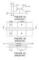
- One way to implement such a programmable switchis to employ a “switch-sense cell” as shown in FIGS. 1A through 1C . This cell is used in the ProASIC, APA, and PA3 families of FPGA integrated circuits manufactured and marketed by Actel Corporation.
- a small sense transistor device and a larger switch transistor deviceshare a single floating gate. The sense device is used to program and read a configuration bit. Both transistors are connected to a control gate associated with a word line. The source and drain of the sense device are connected to bit lines for programming and erasing the cell.
- the switch deviceis inserted in a signal path of the programmable routing.
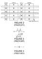
- FIG. 2A general scheme for layout of an FPGA using a switch-sense cell is shown in FIG. 2 .
- Many of the switchesdrive logic inputs. Flash devices must be separated from CMOS logic by a minimum separation.
- An area-efficient layoutwill thus intersperse horizontal bands of logic with horizontal bands of switches, with many rows of switches bunched together in one band. Grouping the rows of switches into fewer bands will reduce area wasted by switch-logic spacing, but tends to lengthen the connecting wires.
- Flash devicescan also be used indirectly, controlling the gate of an NMOS pass device that serves as the switch.
- One way to do thisis the push-pull arrangement, shown in FIG. 3 .
- the switchis controlled by turning on one or the other of the flash devices.
- One flash devicepushes the gate of the switch to ground, shutting the switch off.
- the other devicepulls the gate of the switch to a voltage level sufficient to turn it on.
- the off resistance of the flash devicesmust be high so that static current is kept low. But the push-pull cell does not require as low an on resistance as does the switch-sense cell.
- U.S. Pat. No. 7,430,137describes this and other related push-pull and cross-coupled cells whereby flash devices control NMOS pass gates or complementary NMOS/PMOS pass gates.
- flash devicescan be used either directly or indirectly to make programmable routing switches for FPGAs and other programmable logic devices, they do have a number of limitations. The need to separate flash devices from logic is noted above. In addition, about 12 extra masks are required to manufacture flash devices as compared to ordinary CMOS devices. They also require high voltages ( ⁇ 18V in current technology) to program and erase. They occupy space on the silicon substrate. Flash devices are radiation tolerant to some extent, but are not completely immune to the effects of radiation. Integrating flash technology into a CMOS process may alter the performance of the ordinary CMOS transistors, and requires re-optimizing the integrated process.
- SONOS devicesare similar to flash devices. They require fewer masks to manufacture, and have lower but still significant programming voltages (currently around 8V). SONOS devices are not suitable for use in the signal path of a programmable logic device due to their high on-state resistance and the fact that their state can be altered (or “disturbed”) if the current passing through them gets too high. However SONOS devices can be used to form a push-pull cell, as described in, for example, U.S. Pat. No. 6,144,580.
- PCMphase change memory
- Magnetic RAM (MRAM) devicesare two-terminal memory devices that may be programmed or erased by applying a magnetic field generated by passing current through an adjacent addressing line. Examples of MRAM devices are those manufactured by EverSpin Technologies, Inc. of Chandler, Ariz. MRAM devices have a very low off-to-on resistance ratio of about 1.3.
- Resistive RAMis a general name for two-terminal reprogrammable devices that can be set to either a low or high resistance state. These devices are based on reversible physical phenomena.
- RRAMgenerally consists of a dielectric layer disposed between two electrodes. Some types of RRAM conduct by forming a distinct filament in a limited area of the dielectric. Other types of RRAM conduct by changing the properties of the dielectric throughout its area. Although many types of RRAM devices have been proposed over the years, as yet none of them has been proven to be reliable and manufacturable in practice.
- Bipolar resistive RAM devicesare two-terminal reprogrammable devices that exhibit hysteresis. They enter a low-resistance “on” state when voltage (and current) exceeding a certain threshold is applied in one direction and enter a high-resistance “off” state when voltage exceeding a certain threshold is applied in the opposite direction.
- FIG. 4shows a generic representation of a bipolar RRAM device. The device would turn on when V2 ⁇ V1 exceeds a positive threshold, such as 2 volts.
- bipolar RRAMOne important category of bipolar RRAM are the “solid electrolyte” devices, also known as “conductive-bridging RAM” (CBRAM) and “programmable metallization cells” (PMC).
- CBRAMconductive-bridging RAM
- PMCprogrammable metallization cells
- the memory dielectricis a chalcogenide or glass material. Rather than isolating the dielectric between inert electrodes, one of the electrodes serves as a source of mobile ions that are intended to migrate into the dielectric material.
- the ionsare typically Ag or Cu.
- the ionscan form a conductive filament from one electrode to another through the intervening dielectric material.
- Such deviceshave been described in the literature. For example, see Qimonda, “Conductive Bridging Memory Development from Single Cells to 2 Mbit Memory Arrays”, 8th Non-Volatile Memory Technology Symposium, Nov.
- CBRAMConductive bridging RAM
- bipolar RRAM devicesinclude the “memristor” developed at Hewlett Packard Labs, described in Nature 453, 80-83 (1 May 2008); the “conductive metal oxide” (CMOx) memory cell developed at Unity Semiconductor, described in “Scalable Non-Volatile Cross-Point Memory based on Dual-Layer Oxide Memory Elements”, Rene Meyer, 9th Annual Non-Volatile Memory Technology Symposium, Nov. 11-14, 2008, Pacific Grove, Calif.; ZnCdS reprogrammable “anti-fuses” for FPGAs, described in United States Published Patent Publication 2008/0211540.
- CMOxconductive metal oxide
- Unity Semiconductordescribed in “Scalable Non-Volatile Cross-Point Memory based on Dual-Layer Oxide Memory Elements”, Rene Meyer, 9th Annual Non-Volatile Memory Technology Symposium, Nov. 11-14, 2008, Pacific Grove, Calif.
- ZnCdS reprogrammable “anti-fuses” for FPGAsdescribed in United States Published Patent Publication 2008/0211540.
- off-state resistanceTo make a programmable logic device such as an FPGA with acceptable static power, the off resistance must be high (preferably greater than 100 Gohm in current technology). If the device is used directly as a switch, devices that remain off may have the ordinary logic voltage (currently 1.0 to 1.2V) across them and must be reliably able to withstand that voltage. If the device is used in a push-pull cell, the off device will also have a DC voltage of this magnitude or greater across it. For use directly as a switch, the on-state resistance needs to be less than a few Kohm. The requirements for a push-pull cell are not as stringent.
- the enduranceshould be at least 1000 cycles, preferably 100K cycles or more.
- the magnitude and direction of voltage and current the device can tolerate without risk of disturbing its stateis also an important characteristic.
- the retention timeis also important. Retention time should be at least 10 years, across a stated range of temperature or other operating conditions.
- resistive RAMOther forms of resistive RAM are known which are unipolar, i.e. the program and erase voltages are applied in the same direction but are of different magnitude. Examples include devices described in: “Erase Mechanism for Copper Oxide Resistive Switching Memory Cells with Nickel Electrode”, Int'l Electron Devices Meeting, 2006, pp. 1-4; “Highly Scalable Non-volatile Resistive Memory using Simple Binary Oxide Driven by Asymmetric Uni-polar Voltage Pulses”, IEDM 2004.
- FIG. 5illustrates this problem in an RRAM device formed using a copper metal technology.
- Copper conductor 10is surrounded by Cu barrier layer 12 and is formed in inter-metal dielectric layer 14 .
- a SiN etch stop layer 16is planar with the top surface of the copper metal layer 10 .
- Layers 18 and 20are formed above the surface of copper conductor 10 and SiN layer 16 .
- Layers 18 and 20are the memory cell dielectric and its electrode and can be formed in either order.
- FIG. 5shows a somewhat exaggerated view of how the seam 22 , a gap that is sometimes left as metal fills the space of the via, causes bends in the layers 18 and 20 disposed above the metal.
- the bendsmake the layers deviate from an ideal flat shape.
- the site of the bendcan become the thinnest point of the layer as indicated by arrows 24 and 26 in layers 18 and 20 . Since the electric field across a layer is strongest at its thinnest point, the electrical properties of the memory cell become less predictable as a result of the thinned out layers caused by the unpredictable filling of the seam 22 .
- Prior Art FPGA architecturesinclude SRAM FPGA Architectures.
- the SRAM cellconsists of two inverters in a ring and two addressing devices.
- One output of the SRAM cell, or both complementary outputs,may be used to drive the gates of pass devices serving as programmable routing switches.
- the output of the SRAM cellmay be buffered before driving the pass device gates.
- the supply voltage of the SRAMsmay be above that used in the logic so that the NMOS pass device can pass a full rail signal and the level restoration pull-up device can be omitted.
- Recent SRAM-based FPGA architectureshave organized the programmable routing so that each routing track is driven by a single buffer and the buffer is driven by a multiplexer that selects one of the possible alternative input signals. See Lemieux, Int'l Conf. Field Programmable Tech., 2004, FIGS. 4 (right hand side) and 7 .
- the Xilinx Spartan 3N FPGAincludes a non-volatile memory chip in the same package as an SRAM FPGA chip.
- the XP2 FPGAs from Lattice Semiconductorprovide non-volatile flash memory blocks adjacent to an SRAM FPGA on the same chip.
- the bulk NVMmay be made available for read or read/write operations by the user's logic as well.
- Flash FPGA Architectureis typified by the architecture of the flash-based FPGAs from Actel Corporation.
- certain flash FPGAssuch as Actel's Fusion products, also provide a large block of bulk NVM storage that may be accessed by the user's logic.
- NVM blocksare large in size and limited in number (typically only one). This limits the ways the NVM storage can be applied in user designs, e.g. by limiting the bandwidth or number of ports of the NVM storage.
- U.S. Pat. No. 7,402,847discloses examples of solid electrolyte RRAM devices and ways they can be used to make a crossbar interconnect suitable for FPGA routing.
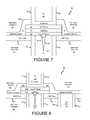
- this referencediscloses a back-to-back arrangement of two RRAM devices to form a programmable switch, as shown in FIGS. 7-10 .
- the back-to-back arrangementhelps reduce the chance of disturbing the state of off switches during normal operation since the voltage threshold necessary to program the switch to a conducting state is roughly doubled.
- an additional tristate driver( 1106 or 1108 ) is needed for every routing track ( 204 or 206 ) carrying signals that are connected by the programmable switch ( 1102 ). This takes extra area. In typical FPGA architectures many if not most tracks are driven by the outputs of logic cells or routing buffers. If the tristate driver used for programming a track is turned on it might fight with the logic or routing buffer output that normally drives the same track. Of course, some means could be provided to override or disconnect the normal output, but this generally costs area and delay.
- routing architectureis a partial crossbar matrix with programmable switches at the locations where vertical and horizontal tracks cross. There is no provision for tracks that are not linear in either a horizontal or vertical direction. This limits the performance and routability of the architecture.
- routing tracksmay be on the order of 100 to 1000 um long, and have a capacitance of 0.2 fF per um.
- the on-resistance of a programmable switchcan be on the order of 10 2 to 10 6 ohms.
- the RC time constantis thus 2 nsec to 0.2 msec. This is comparable to or much larger than a typical clock period at which it is desired to operate the circuit, say 2 nsec.
- significant voltagesmay occur across a programmed switch, which may cause its resistance to increase (read disturb of on-switches).
- the common anodeis on the upper layer of metal. This is inefficient for layout, since the common terminal of the two devices comprising the switch will need to be connected to an addressing transistor through a contact on the lowest layer of metal.
- U.S. Pat. No. 7,511,532describes a push-pull cell using solid-electrolyte RRAM devices in a back-to-back arrangement (see FIG. 23A ). Because of the back-to-back arrangement and the particular polarity chosen, pullup devices that are turned off are subject to DC stress during operation that would tend to turn them on.
- United States Patent Publication 2007/0165446discloses a way to use phase change or solid electrolyte RRAM cells to make SEU hardened SRAM cells.
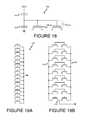
- FIG. 1Ais a circuit diagram showing a prior art switch-sense cell employed to implement a programmable switch.
- FIGS. 1B and 1Care, respectively, top and cross sectional views of the prior art switch-sense cell of FIG. 1A .
- FIG. 2is a layout diagram showing a general scheme for layout of a prior art programmable logic device using a switch-sense cell such as the one of FIG. 1 .
- FIG. 3is a diagram showing the use of prior art flash devices to control the gate of an NMOS pass device that serves as a switch.
- FIG. 4is a diagram showing a generic representation of a prior art bipolar RRAM device.
- FIG. 5is a diagram illustrating how a gap that is sometimes left as metal fills the space of a via, causes bends in the layers disposed above the metal and deleteriously affecting prior-art RRAM devices.
- FIG. 6is a cross-sectional diagram illustrating a resistive RAM device according to one aspect of the present invention.
- FIG. 7is a cross-sectional diagram illustrating a resistive RAM device according to another aspect of the present invention.
- FIG. 8is a cross-sectional diagram illustrating a resistive RAM device according to another aspect of the present invention.
- FIG. 9is a cross-sectional diagram illustrating a resistive RAM device according to another aspect of the present invention.
- FIG. 10is a cross-sectional diagram illustrating a resistive RAM device according to another aspect of the present invention.
- FIG. 11is a cross-sectional diagram illustrating a resistive RAM device according to another aspect of the present invention.
- FIG. 12is a cross-sectional diagram illustrating a resistive RAM device according to another aspect of the present invention.
- FIG. 13is a diagram of an illustrative multiplexer according to the present invention.
- FIG. 14is a cross sectional diagram of a back-to-back RRAM switch.
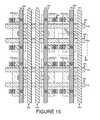
- FIG. 15is a layout diagram illustrating a simple, regular layout scheme for multiplexers according to the present invention.
- FIG. 16is a layout diagram showing a first portion of a more dense layout for a multiplexer.
- FIG. 17is a layout diagram showing a second portion of the multiplexer layout of FIG. 16 .
- FIG. 18is a schematic diagram shows a push-pull RRAM cell in accordance with one aspect of the present invention.
- FIGS. 19A and 19Bare diagrams showing alternative ways of forming multiplexers.
- FIG. 20is a diagram that illustrates a front-to-back push-pull cell according to the present invention.
- FIG. 21is a cross sectional view of one alternative push-pull cell layout according to the present invention.
- FIG. 22is a cross sectional view of another alternative push-pull cell layout according to the present invention.
- FIG. 23is a cross sectional view of a first additional alternative structure for the front-to-back cell according to the present invention.
- FIG. 24is a cross sectional view of a second additional alternative structure for the front-to-back cell according to the present invention.
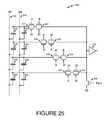
- FIG. 25is a schematic diagram showing front-to-back push-pull pairs of bipolar RRAM devices used to configure a look-up table (LUT) without the usual addressing devices.
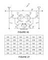
- FIG. 26is a schematic diagram of an illustrative nonvolatile memory constructed around a resistive random access memory cell according to one aspect of the present invention.
- FIG. 27shows a possible arrangement of RAM blocks, NVM blocks and logic tiles to form an FPGA core according to the present invention.
- RRAM devices according to the present inventionare disclosed.
- the RRAM devices according to the present inventionare more manufacturable and are more reliable than prior-art RRAM devices.
- FIG. 6a cross-sectional diagram shows the structure of an illustrative RRAM device 30 according to the present invention presenting one way to reduce the seam problem illustrated in FIG. 5 .
- the RRAM device 30 illustrated in FIG. 6can be incorporated into a process using tungsten-filled vias.
- RRAM device 30is formed over a tungsten via 32 .
- Tungsten via 32is surrounded by a barrier layer 34 and is formed in inter-metal dielectric layer 36 .
- a CMP stop layer 38is formed over the top of the inter-metal dielectric layer 36 and is used in the process employed to planarize the top of tungsten plug 32 as is known in the art. SiN or SiC are commonly employed as CMP stop layers.
- CMP stop layers described with reference to FIG. 6may not be required and are optional. Their use or non-use will depend on the CMP technology used by the manufacturer. Some CMP processes may be able to have a timed polish step and do not need the CMP stop layer. This is preferred because it makes the process of depositing the dielectric layers simpler. In addition, the removal of SiN which has a dielectric constant of 7 and replaced with silicon oxide which has a dielectric constant of 4 is preferred and will reduce the coupling capacitance of the metal layers, thus improving the speed performance of the product.
- barrier metal layer(s) 40may be formed from a material such as Ta, TaN, Ti or TiN, W or other suitable material.
- a dielectric layer 42is formed above barrier metal layer 40 .
- the dielectric layer 42may be formed from GeS or other chalcogenides, glasses, etc., known to serve a similar function in a solid electrolyte RRAM device.
- a top electrode or ion source 44is formed over the dielectric layer 42 and is formed from a material such as Ag, since Cu may be difficult to plasma etch.
- the stack of layers 40 , 42 , and 44is etched to form an aligned stack.
- a dielectric barrier layer 46 formed from a material such as SiN or SiCis formed over the defined stack.
- a via 50is formed in the dielectric barrier layer 46 to expose the upper surface of ion source layer 44 .
- a barrier metal layer 48is then formed over the dielectric barrier layer and makes contact with ion source layer 44 in via 50 .
- the top metal 52may be formed from a material such as Al, Cu or other metal used for interconnect layers in integrated circuits.
- FIG. 7a cross-sectional diagram shows the structure of another illustrative RRAM device 60 according to the present invention presenting a way to reduce the seam problem illustrated in FIG. 5 .
- FIG. 7shows an illustrative embodiment of a structure for a copper metallization process.
- RRAM device 60is formed over a copper via 62 .
- Copper via 62is surrounded by a Cu barrier layer 64 and is formed in inter-metal dielectric layer 66 .
- a CMP stop layer 68is formed over the top of the inter-metal dielectric layer 36 and is used in the process employed to planarize the top of copper plug 62 as is known in the art.
- SiN or SiCare commonly employed as CMP stop layers.
- one or two layers 70 of a barrier metalare formed above the via 62 and extend beyond the edges of the via and over the CMP stop layer 68 .
- the barrier metal layer(s) 70may be formed from a material such as Ta, TaN, Ti or TiN, W or other suitable material.
- a dielectric layer 72is formed above barrier metal layer 70 .
- the dielectric layer 72may be formed from GeS or other chalcogenides, glasses, etc., known to serve a similar function in a solid electrolyte RRAM device.
- a top electrode or ion source 74is formed over the dielectric layer 72 and is formed from a material such as Ag, since Cu may be difficult to plasma etch.
- the stack of layers 70 , 72 , and 74is etched to form an aligned stack.
- a dielectric barrier layer 76 formed from a material such as SiN or SiCis formed over the defined stack.
- Another inter-layer dielectric layer 78is then formed over dielectric barrier layer 76 .
- a viais formed in the inter-layer dielectric layer 78 and dielectric barrier layer 76 to expose the upper surface of ion source layer 74 .
- a top copper metallization layer including copper 80 surrounded by Cu barrier layer 82is then formed in the inter-layer dielectric layer 78 and makes contact with ion source layer 74 in the via.
- an additional barrier metal layermay optionally be added above the ion source layer 74 to protect the ion source material from being etched during subsequent processing.
- FIG. 8a cross-sectional view shows an idealized rendering of a preferred embodiment of such a structure.
- RRAM device 90 of FIG. 8is formed over a copper wire 92 .
- Copper wire 92is surrounded by a Cu barrier layer 94 and is formed in inter-metal dielectric layer 96 .
- Another copper wire 98is shown having been formed in inter-metal dielectric layer 96 and is surrounded by a Cu barrier layer 100 .
- the Cu barrier materialmay be Ta, TaN, Ti or TiN.
- the copper wire 92serves as the ion source.
- a CMP stop layer 102is formed over the top of the inter-metal dielectric layer 96 and is used in the process employed to planarize the top of copper wires 92 and 98 as is known in the art. SiN or SiC are commonly employed as CMP stop layers.
- a dielectric layer 104is formed above the copper wire 92 and extend past its edges over CMP stop layer 102 .
- the dielectric layer 104may be formed from GeS or other chalcogenides, glasses, etc., known to serve a similar function in a solid electrolyte RRAM device.
- At least one barrier metal layer 106is formed above dielectric layer 104 .
- the barrier metal layer(s) 106may be formed from a material such as Ta, TaN, Ti or TiN, W or other suitable material.
- the stack of layers 104 , and 106is etched to form an aligned stack.
- a dielectric barrier layer 108 formed from a material such as SiN or SiCis formed over the defined stack.
- Another inter-layer dielectric layer 110is formed over the dielectric barrier layer 108 .
- a viais formed in the inter-layer dielectric layer 110 and the dielectric barrier layer 108 to expose the upper surface of barrier metal layer 106 .
- a top copper metallization layer including copper 112 surrounded by Cu barrier layer 114is then formed in the via and makes contact with barrier metal layer 106 at the bottom of the via.
- FIG. 9a cross sectional view shows another embodiment of an RRAM cell 120 having a copper-filled via instead of a wire below the memory cell.
- the memory cell 120is similar to memory cell 90 of FIG. 8 except for the narrower width of the copper via as compared to the width of the copper wire 92 of FIG. 8 .
- RRAM device 120 of FIG. 9is formed over a copper via 122 .
- Copper via 122is surrounded by a Cu barrier layer 124 and is formed in inter-metal dielectric layer 126 .
- the Cu barrier materialmay be Ta, TaN, Ti or TiN.
- the copper via 122serves as the ion source.
- An optional CMP stop layer 128is formed over the top of the inter-metal dielectric layer 126 and is used in the process employed to planarize the top of copper via 122 as is known in the art. SiN or SiC are commonly employed as CMP stop layers.
- a dielectric layer 130is formed above the copper via 122 and extend past its edges over CMP stop layer 128 .
- the dielectric layer 130may be formed from GeS or other chalcogenides, glasses, etc., known to serve a similar function in a solid electrolyte RRAM device.
- a barrier metal layer 132is formed above dielectric layer 130 .
- the barrier metal layer 132may be formed from a material such as Ta, TaN, Ti or TiN, W or other suitable material.
- the stack of layers 130 and 132is etched to form an aligned stack.
- a dielectric barrier layer 134 formed from a material such as SiN or SiCis formed over the defined stack.
- Another inter-layer dielectric layer 136is formed over the dielectric barrier layer 134 .
- a viais formed in the inter-layer dielectric layer 136 and the dielectric barrier layer 134 to expose the upper surface of the barrier metal layer 132 .
- a top copper metallization layer including copper 138 surrounded by Cu barrier layer 140is then formed in the via and makes contact with the top of barrier metal layer 132 at the bottom of the via.
- the present inventionhas several advantageous features.
- several embodiments of the inventionuse copper wires or vias that are already present for interconnect metallization as the ion source in a solid electrolyte cell.
- the ion sourceis at the bottom of the device rather than the top as in some of the prior-art implementations. This may be advantageous for layout of certain switch cells, where it may be desirable for the common electrode to be at the bottom of the structure.
- the structures disclosed in FIGS. 8 and 9do not specifically address the seam problem. There are other embodiments of the present invention that address the seam problem with these types of structures.
- FIG. 10shows a raised plug structure for RRAM and shows the impact of the seam on the layers above for the structure using the underlying Cu Via material as the ion source.
- RRAM device 150 of FIG. 10is formed over a raised copper via 152 .
- Copper via 152is surrounded by a Cu barrier layer 154 , is formed in inter-metal dielectric layer 156 , and extends beyond the top surface of CMP stop layer 158 .
- the Cu barrier layer 154may be Ta, TaN, Ti or TiN.
- the corners of barrier layer 154are rounded (e.g., by CMP) to allow for increased thickness of the dielectric at point 172 .
- the raised copper via 152serves as the ion source.
- a CMP stop layer 158is formed over the top of the inter-metal dielectric layer 156 and is used in the process employed to raise the top of copper via 152 as is known in the art. SiN or SiC are commonly employed as CMP stop layers.
- a dielectric layer 160is formed above the raised copper via 152 and extends past its edges over CMP stop layer 158 .
- the dielectric layer 160may be formed from GeS or other chalcogenides, glasses, etc., known to serve a similar function in a solid electrolyte RRAM device.
- a barrier metal layer 162is formed above dielectric layer 160 .
- the barrier metal layer 162may be formed from a material such as Ta, TaN, Ti or TiN, W or other suitable material.
- Another inter-layer dielectric layer 164is formed over the dielectric barrier metal layer 162 .
- a viais formed in the inter-layer dielectric layer 164 to expose the upper surface of the raised copper via 152 .
- a top copper metallization layer including copper 166 surrounded by Cu barrier layer 168is then formed in the via and makes contact with the top of barrier metal layer 162 at the bottom of the via.
- the thinnest point of the layers over the copper via plug in the embodiment of FIG. 10is no longer at the seam 170 . Instead, the thinnest point is now at the circumference of the plug as shown at arrows 172 , where it can be more easily controlled during manufacturing. This technique is especially effective for those types of RRAM in which a filament is formed in the on state.
- the structure shown in FIG. 10results from adding one CMP step to the standard copper metallization process.
- This additional stepis a CMP dielectric polishing step which reduces the thickness of the CMP stop layer 158 , leaving the copper via raised relative to the top of the CMP stop layer 158 , and rounding the top corners of the copper via 152 .
- SiNis the preferred material for CMP stop layer 158
- SiC or the inter-layer dielectric materialmay also be used.
- the raised plugmay be used in combination with the other structures described previously. For instance, even if there is a barrier metal layer between the raised plug and the dielectric, the raised plug will still shift the thinnest point of the dielectric to the circumference of the plug, as shown in FIG. 11 .
- a raised copper via plug structure for an RRAM Devicewhere the via is not used as the ion source.
- a full stack structure RRAM device 180is formed over a raised copper via 182 .
- Copper via 182is surrounded by a Cu barrier layer 184 , is formed in inter-metal dielectric layer 186 , and extends beyond the top surface of CMP stop layer 188 .
- the Cu barrier layer 184may be Ta, TaN, Ti or TiN.
- the raised copper via 182does not serve as the ion source in this embodiment.
- the CMP stop layer 188is formed over the top of the inter-metal dielectric layer 186 and is used in the process employed to raise the top of copper via 182 above its upper surface as is known in the art. SiN or SiC are commonly employed as CMP stop layers.
- a barrier metal layer 190is formed above the raised copper via 152 and extend past its edges over CMP stop layer 158 .
- the barrier metal layer 160may be formed from a material such as Ta, TaN, Ti or TiN, W or other suitable material.
- a dielectric layer 192is formed above barrier metal layer 190 .
- the dielectric layer 192may be formed from GeS or other chalcogenides, glasses, etc., known to serve a similar function in a solid electrolyte RRAM device.
- An ion source layer 194is formed over the dielectric layer 192 and is formed from a material such as Ag.
- Another inter-layer dielectric layer 196is formed over the ion source layer 194 .
- a viais formed in the inter-layer dielectric layer 196 to expose the upper surface of the ion source layer 194 .
- a top copper metallization layer including copper 198 surrounded by Cu barrier layer 200is then formed in the via and makes contact with the top of barrier metal layer 196 at the bottom of the via.
- layers 190 - 194may be extended as shown in FIG. 11 , in one or more directions, or may be “cut” as shown in FIG. 9 on one or more sides.
- the thinnest point of the layers over the copper via plug in the embodiment of FIG. 11is no longer at the seam 202 . Instead, the thinnest point is now at the circumference of the plug as shown at arrows 204 , where it can be more easily controlled during manufacturing. This technique is also especially effective for those types of RRAM in which a filament is formed in the on state.
- FIG. 12shows a portion of the embodiment illustrated in FIG. 11 .
- This filler techniquecould be applied to all the FIG. 6-11 structures.
- FH Structures from the embodiment of FIG. 11 that are also shown in FIG. 12are designated by the same reference numerals used in FIG. 11 to designate those structures.
- the issue of the seam in the copper viacan be further improved further by adding a fill material 206 in the seam 202 .
- the fill material 206can be either a conductive or non-conductive material as long as it seals the seam from contamination escaping and the fill material 206 itself does not contaminate the RRAM dielectric.
- Non-conductive fill materialcan be used since after most of it is removed in the final CMP step the filler will no longer cover the outer portion of the via.
- Suitable fill materialsmay include SiO2 or SiN, barrier metals such as Ti, Ta, W, TiN, TaN, or other materials, even Cu.
- the preferred deposition methodis CVD due to its superior step coverage, although PVD could be used as well.
- the depositionshould occur just before the final CMP step used to raise the via plug 182 as described with reference to the embodiments of FIGS. 10 and 11 .
- the final CMP stepwould then remove the sealant fill material from the top and corners of the metal line or via 182 while leaving it remaining in the seam to smooth out the metal line or via and thereby improve the control and yield of the RRAM cell.
- the critical dielectric and adjacent layersare preferably not deposited in a via hole, as was the case in some prior art RRAM structures such as FIGS. 1, 2 and 4 of U.S. Pat. No. 6,865,117. Depositing the materials in a via hole results in irregularities at the corners of the hole, as well as other problems. Instead the critical layers are formed by CVD (or PVD) deposition and etching.
- the critical layersextend horizontally past the edges of the metal conductor (tungsten or copper via or wire) below. This is preferred to provide a higher yield structure with less chance of contamination or defects.
- the RRAM devices disclosed hereinmay be particularly suitable for incorporating into switch cells for use as configuration memory or in other circuits such as multiplexers in programmable logic devices such as FPGAs.
- switch cellsmay also be useful with other types of NVM devices.
- RRAM switch cellIn order to create a programmable logic device such as an FPGA using an RRAM device structure, it is necessary to find a suitable way to use the structure to make a programmable switch.
- the configuration of a RRAM switch cellwill depend somewhat on the characteristics of the RRAM device employed, as described below.
- RRAM devicesthat have high off resistance, have on resistance on the order of 10 K ⁇ or below, are not disturbed by logic signal currents in the on state, and have a sufficiently high threshold voltage to avoid disturb of the off state
- two RRAM devicescan be employed in a back-to-back configuration similar to the configuration disclosed in U.S. Pat. No. 7,402,847.
- thisrequires that the limitations (mentioned above) of the prior art scheme are overcome as disclosed herein.
- an architecture for multiplexer cellsmay be implemented using back-to-back RRAM devices in accordance with the present invention.
- FIG. 13an illustrative embodiment of a multiplexer 210 formed using back-to-back RRAM according to the present invention is shown. While the particular example of FIG. 13 shows a three-input multiplexer, persons of ordinary skill in the art will appreciate that multiplexers having an arbitrary number of inputs can be fabricated using the principles of the present invention.
- Multiplexer 210has its inputs connected to routing tracks driven by buffers 212 , 214 , and 216 .
- the output of multiplexer 210drives buffer 218 .
- Buffer 218in turn drives another routing track.
- the routing track T 1 driven by buffer 212is coupled to a first back-to-back RRAM configuration including RRAM devices 220 and 222 .
- the input of buffer 218is coupled to the first back-to-back RRAM configuration.
- the drain of an address transistor 224is coupled between the common terminals of the RRAM devices 220 and 222 .
- Address transistor 224is located in column x and row y.
- the gate of address transistor 224is coupled to a row y address line RAy.
- the source of address transistor 224is connected to a column x address line CAx indicated at reference numeral 226 .
- the routing track T 2 driven by buffer 214is coupled to a second back-to-back RRAM configuration including RRAM devices 228 and 230 .
- the input of buffer 218is also coupled to the second back-to-back RRAM configuration.
- the drain of an address transistor 232is coupled between the common terminals of the RRAM devices 228 and 230 .
- the gate of address transistor 232is coupled to another row address line.
- the source of address transistor 232is coupled to the column x address line CAx at reference numeral 226 .
- the routing track T 3 driven by buffer 216is coupled to a third back-to-back RRAM configuration including RRAM devices 234 and 236 .
- the input of buffer 218is also coupled to the third back-to-back RRAM configuration.
- the drain of an address transistor 238is coupled between the common terminals of the RRAM devices 234 and 236 .
- the gate of address transistor 238is coupled to another row address line.
- the source of address transistor 238is coupled to the column x address line CAx at reference numeral 226 .
- each buffer 212 , 214 , 216 , and 218is provided with a single programming transistor, indicated at reference numerals 240 , 242 , 244 , and 246 , respectively.
- the gate of each programming transistoris tied to a program-enable signal PE and the source of each programming transistor is tied to a programming level signal PL.
- PE and PLmay be global signals; it is not necessary to have separate signals to address individual buffers or even subsets of buffers, which results in a further area savings.
- Each of the buffers 212 , 214 , 216 , and 218themselves can be used to force their output to the same state as PL, so the programming transistors are only needed on half rather than all of the nets in contact with the programmable switches, saving area and complexity.
- the common terminal of the two memory devices ( 220 and 222 , 228 and 230 , and 234 and 236 ) comprising each switchis preferentially (and in contrast to the prior art) the terminal connected to the lower layer of metal, as shown in FIG. 14 .
- the RRAM deviceswould preferably be between metal 1 and metal 2, rather than the upper layers of metal as in the prior art. This leaves the upper layers free for long-distance routing despite the heavy connectivity between the RRAM devices and the addressing transistors, provided at each common terminal.
- Diffusion 252forms the source of the transistor, coupled to column address line CAx at reference numeral 254 and diffusion 256 forms its drain. Its gate 258 is coupled to the row-address line RAy at reference numeral 260 .
- Contact 262connects diffusion 256 to a portion of first metal layer 264 .
- 266couples the first metal layer 264 to terminal 268 of the first RRAM device.
- the second terminal 270 of the first RRAM deviceis formed from a portion of a second metal layer.
- 272couples the first metal layer 264 to terminal 274 of the second RRAM device.
- the second terminal 276 of the first RRAM deviceis also formed from a portion of a second metal layer.
- the first terminals 268 and 274 of the RRAM devicesare commonly connected to the segment 264 of the first metal line.
- the parasitic capacitance of the multiplexer output (Mout)must be kept as small as possible. Immediately buffering this signal before it drives other routing tracks helps achieve this goal. But this is not sufficient.
- the switches comprising the multiplexer and the buffermust be laid out very close together. With a good layout in 65 nm technology, the capacitance of Mout would probably be dominated by the input (gate) capacitance of the buffer, which typically is only a few fF. Each routing buffer can then fan out through a routing track to various switches in other multiplexers.
- routing tracksi.e. electrical nodes driven by a buffer or logic cell output
- all routing tracksi.e. electrical nodes driven by a buffer or logic cell output
- FIGS. 13 and 14are arranged in an array of rows and columns.
- the gates of all addressing transistors for switches in row yare connected to a row address line RAy.
- the sources of all addressing transistors for switches in column xare connected to a column address line CAx.
- FIG. 13shows all switches in the multiplexer as being in the same column, that this is not necessarily the case.
- Such skilled personswill also appreciate that the roles of row and column lines may be swapped.
- switch x,ymay be programmed as follows. PE is raised. RAy is raised. PL is set to either logic 0 or 1 and CAx is driven to an appropriate voltage to apply the necessary forward or reverse bias to switch x,y to put it in the on or off state as desired. CAx′ for all x′ ⁇ x is set to the same voltage as PL to avoid biasing unselected switches.
- programmable logic devicessuch as FPGAs contain logic cells such as look-up-tables or flip-flops as well as routing buffers. Additional circuitry analogous to the programming devices must be provided to ensure that logic cell inputs and outputs in contact with programmable switches are also driven to PL during programming. Persons skilled in the art will understand how to configure such additional circuitry according to the needs of any particular integrated circuit architecture.
- CMOS pass gatecomposed of a parallel p and n device may be used, instead of the single NMOS transistor as shown in FIGS. 13 and 14 .
- PLmay be fixed at logic 0 or fixed at logic 1.
- the routing bufferscan be equipped with power switches or the buffers can be powered from a common switched supply. If the power supply (V DD ) of the buffer is switched, and it is desired to force the buffer outputs to ground for programming, a small pulldown device gated by PE can be added to pull the buffer output to ground. To enter programming mode, the power supply is turned off by lowering it to ground, then the pulldowns are activated to force the buffer outputs to 0. This technique is also applicable to logic cell outputs as well as all routing buffer outputs.
- a few variationsare possible for controlling the common terminals of the programmable switches. Although a single addressing transistor has been employed to drive the common terminals of the programmable switches, it may be necessary to use two transistors depending on the voltages required. For instance, a complementary pair of NMOS and PMOS transistors forming a CMOS pass gate may be used. In addition, a two-transistor capacitive boosting scheme, similar to the addressing devices in Actel antifuse FPGAs, may also be employed. The RA/CA and PE/PL addressing schemes may also be used to observe and/or control the circuitry in the FPGA for testing or debugging purposes.
- asynchronous FPGAIf used with a synchronous FPGA, the back-to-back pairs of devices that are in an off state are subject to static stress since there may be logic 0 and logic 1 on opposite ends of the switch for an unlimited period during operation.
- Using asynchronous FPGA logicmay be advantageous in that signals transition for short periods of time then return to a common resting state. This tends to reduce the static stress, at the cost of additional transitions.
- the row-address lines 280are run horizontally.
- One or more rows of switchesare interspersed with rows of buffers and logic, so the logic does not interrupt the row-address lines and the row-address lines can run continuously across the array in polysilicon.
- the column address linesare shown running vertically at reference numerals 282 and are located in the metal 1 layer.
- a single switch cellis shown inside dashed lines 284 .
- the buffer driven by a multiplexer output such as Moutis preferentially placed just above or below the corresponding switches. This way the Mout node is very compact, keeping its capacitance limited.
- Two of the adjacent Mout lines shown at reference numerals 286 running vertically in the metal 2 layermay be connected to reach even more switches without unduly lengthening the Mout line. Although the Mout lines 286 have been shown as continuous, they can be broken where necessary to form two or more smaller muxes.
- the pads of metal 2 provided for connecting the multiplexer inputscan easily be shared if adjacent multiplexers have common input signals.
- the routing tracks supplying inputs to the multiplexerswould be routed on upper layers of metal, or metal 2 or metal 1 where it is still available.
- One of the RRAM devicesis identified at reference numeral 288 .
- the common terminal of the two memory devices comprising a switch(reference numerals 268 and 274 ) is preferably connected to metal 1 (at reference numeral 264 ), it is easy to connect it to the corresponding addressing transistor. This is shown at reference numeral 288 , where one of the horizontal fingers of the metal 1 layer passes under the metal 2 layer 286 used as Mout.
- FIG. 16illustrates how metal 1, metal 2 and the switches are arranged to implement a 4-input by 2-output crossbar.
- the column address lines 290run vertically in metal 1.
- the inputs 292 and outputs 294run horizontally in metal 2.
- the outputsare available above and below the row of switches (one switch shown at reference numeral 296 ), so the corresponding routing buffer can be placed nearby.
- All metal 1 and metal 2 tracksrun vertically and horizontally, respectively, which makes the layout efficient and manufacturable. If a full crossbar is not desired, the metal 2 lines can be broken to suit, with incoming signals delivered from higher layers of metal.
- FIG. 17includes the location of the RRAM devices, the polysilicon layers and the metal 1 layer.
- FIG. 17shows how the addressing transistor devices can be laid out beneath the pattern of metal depicted in FIG. 16 .
- the polysilicon layersdefine the transistors where they pass over the diffusion layers in the substrate.
- the back-to-back RRAM cell of the present inventionprovides several advantages over the prior art. It reduces or eliminates read disturb of on switches by limiting maximum capacitance driven through any RRAM device. It replaces the separate tristate driver on each routing track required in the prior art with a single programming transistor, saving area. It avoids fighting between logic or routing buffer outputs and the tristate drivers used for programming in the prior art.
- the layoutis optimized for density and to keep capacitance on Mout small.
- the common terminal of the two devices comprising a switchis connected to the lower rather than the upper layer of metal for improved layout density.
- Prior-art RRAM memoriesusually run the word lines in metal for good write speed. According to the present invention, the word (row-address) lines run continuously in poly for improved layout density.
- a push-pull RRAM cellis disclosed.
- a push-pull cellcan be used where the RRAM devices control an NMOS pass device.
- a basic push-pull RRAM cell, and some variations on itare described, as well as an additional push-pull cell specific to bipolar RRAM. The variations disclosed can be used independently or in combination.
- FIG. 18a schematic diagram shows an illustrative push-pull RRAM cell 300 in accordance with one aspect of the present invention.
- the RRAM devices 302 and 304control one or more NMOS pass transistors 306 and 308 whose sources and drains are connected to routing tracks as known in the art (not shown) and which serve as programmable switches for the programmable logic device.
- the FPGA or other programmable logic deviceis properly programmed, either one or the other but not both of the RRAM devices 302 and 304 is set to conduct.
- RRAM device 302is coupled to ground and, when turned on, pushes the gates of the pass devices to ground to shut them off
- the RRAM device 304is coupled to a positive configuration memory voltage Vcm and, when turned on, pulls the gates of the pass devices up to the configuration memory voltage Vcm to turn them on. Whichever RRAM device is turned is off must not be disturbed by a DC stress from Vcm disposed across it. Whichever of RRAM devices 302 or 304 is turned on must not be disturbed by the currents due to the parasitic coupling capacitance (shown at reference numeral 310 ) as the logic signals on the sources and drains of the NMOS devices rise and fall. Techniques to adhere to these requirements are disclosed below.
- Vcmcan be set somewhat higher than the V DD of the logic; this ensues the pass devices can pass the full level of V DD .
- Vcmcan be the same as V DD , and a level restoring device can be provided on the output side of the pass devices.
- a complementary PMOS pass devicecan be placed in parallel with the NMOS pass device to form a pass gate. The gate of the PMOS device must be produced by inverting the signal on the gate of the NMOS device, or by another push-pull pair programmed into the complementary state of the first pair.
- FIGS. 19A and 19Bshow a 16:1 multiplexer 320 implemented in a one level manner
- FIG. 19Bshows a pair of 8:1 multiplexers 322 and 324 followed by a 2:1 multiplexer 326 .
- the gates of corresponding pass devices in the 8:1 multiplexersare joined, and so can be controlled by the a single push-pull circuit.
- NMOS or PMOS series transistorscan be added to the path to limit the voltage across the RRAM devices.
- An appropriate bias levelmust be provided on the gate of the series transistors during normal operation and during programming and erasing. This idea is described more fully in co-pending patent application Ser. No. 12/828,606, filed on the same day as the present application and incorporated herein by reference, which also discusses its application to other forms of NVM such as SONOS.
- FIG. 18did not specify the polarity of the RRAM devices. But if the RRAM device is bipolar, the RRAM devices can be connected in a front-to-back manner to avoid disturb of the off device.
- FIG. 20a diagram illustrates a front-to-back push-pull cell 330 according to the present invention in more detail.
- Push-pull cell 330includes RRAM devices 332 and 334 coupled between potentials VP and VN at reference numerals 336 and 338 respectively.
- Programming transistor 340is coupled between potential VS and the common terminal G of RRAM deices 332 and 334 .
- the gate of programming transistor 340is coupled to a word line W.
- Push-pull cell 330is shown driving the gates of two switch transistors 342 and 344 , although persons skilled in the art will appreciate that different numbers of switch transistors could be employed depending on circuit needs.
- FIG. 21shows a “back-to-back” arrangement (with the polarity of the pulldown device reversed relative to FIG. 20 ). This uses only two metal pitches, and so would be preferred if read disturb of the off device is not an issue.
- diffusion 352serves as the source of programming transistor 340 ( FIG. 20 ) and is coupled to the potential VS.
- Diffusion 354serves as the drain of the programming transistor.
- Polysilicon line 256serves as the gate of the programming transistor and as a word line.
- Diffusion 358serves as the source of one of the switch transistors of FIG. 20 .
- Diffusion 360serves as the drain of the switch transistor.
- Polysilicon line 362serves as the gate of the switch transistor.
- Contact 364connects the drain of the programming transistor to a segment 366 of a metal-1 line.
- Contact 368connects the gate 362 of the switch transistor to metal-1 line segment 366 .
- Contact 370connects metal-1 line segment 366 to the anode of RRAM device 372 .
- Contact 374connects the cathode of RRAM device 372 to metal-2 line segment 376 .
- Via 378connects metal-1 line segment 366 to the anode of RRAM device 380 .
- Via 382connects the cathode of RRAM device 380 to metal-2 line segment 384 .
- diffusion 392serves as the source of programming transistor 340 ( FIG. 20 ) and is coupled to the potential VS.
- Diffusion 394serves as the drain of the programming transistor.
- Polysilicon line 396serves as the gate of the programming transistor and as a word line.
- Diffusion 398serves as the source of one of the switch transistors of FIG. 20 .
- Diffusion 400serves as the drain of the switch transistor.
- Polysilicon line 402serves as the gate of the switch transistor.
- Contact 404connects the drain of the programming transistor to segment 406 of metal-1 line 406 .
- Contact 408connects the gate 402 of the switch transistor to metal-1 line segment 406 .
- Contact 410connects metal-1 line segment 406 to the anode of RRAM device 412 .
- Contact 414connects the cathode of RRAM device 412 to metal-2 line segment 416 , which is coupled to VP.
- Contacts 418 and 420connect metal-1 line segment 406 to the cathode of RRAM device 422 through metal-2 line segment 424 .
- Contact 426connects the anode of RRAM device 422 to metal-1 line segment 428 , which is coupled to VN.
- FIG. 22shows a “front-to-back” arrangement of RRAM devices 412 and 422 , reflecting the polarities shown in the schematic diagram of FIG. 20 .
- the embodiment shown in FIG. 22takes slightly more area, but, because the RRAM devices 412 and 422 are arranged in a “front-to-back” configuration, avoids disturbing whichever device is off during normal operation.
- Wis set high, VS is set to 0V, VP is set to 2V, and VN is set to 0V.
- Wis set high, VS is set to 2V, VP is set to 2V, and VN is set to 0V.
- Wis a word line controlling a row of switch cells.
- VSis global and VP and VN are dual bit lines controlling a column of switch cells.
- Wis set high (selected) or low (unselected)
- VSis set to 2V
- VPis set to 0V (selected) or 2V (unselected)
- VNis set to 0V (selected) or 2V (unselected). If the selected pulldown is already erased, the selected VN might be raised above 0V as long as it does not become so high as to disturb erased devices in the selected column.
- Wis set high (selected) or low (unselected)
- VSis set to 0V
- VPis set to 2V (selected) or 0V (unselected)
- VNis set to 2V (selected) or 0V (unselected). If the selected pullup is already erased, the selected VP might be lowered below 2V as long as it does not become so low as to disturb erased devices in the selected column.
- VSis the bit line and VP and VN are global signals.
- Wis set high (selected) or low (unselected)
- VSis set to 2V (selected) or 0V (unselected)
- VPis set to 0V
- VNis set to 0V. If the selected pulldown is already erased, VN might be raised above 0V as long as it does not become so high as to disturb erased devices.
- Wis set high (selected) or low (unselected)
- VSis set to 0V (selected) or 2V (unselected)
- VPis set to 2V
- VNis set to 2V. If the selected pullup is already erased, VP might be lowered below 2V as long as it does not become so high as to disturb erased devices.
- Table 1summarizes the programming/erasing tasks and the applied voltages under both alternative connection schemes. Note that selective erasing may be done without programming. However in the second alternative this requires some care to avoid inadvertently disturbing unselected programmed devices (see starred entries), such as precharging the bit lines to 1V or some other suitable voltage between 0 and 2V. Each entry in the table has three symbols specifying the state of VP, G (the gate of the relevant switches), and VN, respectively.
- the front-to-back cell of the present inventionhas several advantages. It allows front-to-back arrangement of bipolar RRAM devices to take advantage of their asymmetrical nature to avoid disturb. It permits applying voltages as shown in Table 1, especially for the programming task. It allows for two particular schemes for assigning VS, VP and VN to global or bit lines.
- a pair of RRAM devicesmay control multiple switches (pass devices).
- RRAM memoriesusually run the word lines in metal for good write speed.
- the word (W) linesmay be run continuously in poly for improved layout density.
- FIG. 23shows two additional alternative structures for the front-to-back cell in a side view. These are intended to eliminate the area penalty imposed by the front-to-back topology.
- the structure shown in FIG. 23uses distinct masking to create RRAM devices of both polarities between metal 1 and metal 2.
- the structure in FIG. 24places RRAM devices in the same orientation between metal 1 and metal 2, and between metal 2 and metal 3.
- the push-pull cell 440 of FIG. 23shows a “front-to-back” arrangement that uses only two metal pitches.
- diffusion 442serves as the source of the programming transistor and is coupled to the potential VS.
- Diffusion 444serves as the drain of the programming transistor.
- Polysilicon line 446serves as the gate of the programming transistor and as a word line.
- Diffusion 448serves as the source of one of the switch transistors.
- Diffusion 450serves as the drain of the switch transistor.
- Polysilicon line 452serves as the gate of the switch transistor.
- Contact 454connects the drain of the programming transistor to a segment 456 of a metal-1 line.
- Contact 458connects the gate 452 of the switch transistor to metal-1 line segment 456 .
- Contact 460connects metal-1 line segment 456 to the anode of RRAM device 462 .
- Contact 464connects the cathode of RRAM device 462 to metal-2 line segment 466 .
- Contact 468connects metal-1 line segment 456 to the cathode of RRAM device 470 .
- Contact 472connects the anode of RRAM device 470 to metal-2 line segment 474 .
- diffusion 482serves as the source of the programming transistor and is coupled to the potential VS.
- Diffusion 484serves as the drain of the programming transistor.
- Polysilicon line 486serves as the gate of the programming transistor and as a word line.
- Diffusion 488serves as the source of one of the switch transistors of FIG. 20 .
- Diffusion 490serves as the drain of the switch transistor.
- Polysilicon line 492serves as the gate of the switch transistor.
- Via 494connects the drain of the programming transistor to a segment 496 of a metal-1 line. Via 498 connects the gate 492 of the switch transistor to metal-1 line segment 496 . Via 500 connects metal-1 line segment 496 to a segment 502 of a metal-2 line. A contact 504 connects segment 502 of the metal-2 line to the anode of RRAM device 506 . Via 508 connects the cathode of RRAM device 506 to a segment 510 of a metal-3 line.
- Via 514connects metal-2 line segment 504 to the cathode of RRAM device 516 .
- Via 518connects the anode of RRAM device 516 to metal-1 line segment 520 .
- FIG. 25a schematic diagram shows a variation of the front-to-back RRAM arrangement, specifically how front-to-back push-pull pairs of bipolar RRAM devices may be used to configure a look-up table (LUT) without the usual addressing devices. Instead, the multiplexer comprising the look-up table is used to address the RRAM devices.
- VPis set to V DD (normal logic power supply) and VN to ground (normal logic ground).
- LUT 520includes pairs of series connected pass gates.
- a first pair of pass gatesincludes pass gates 522 and 524 .
- a second pair of pass gatesincludes pass gates 526 and 528 .
- a third pair of pass gatesincludes pass gates 530 and 532 .
- a fourth pair of pass gatesincludes pass gates 534 and 536 .
- the pass gatesare all coupled to the input of output buffer 538 .
- the connections of the LUT terms A, A!, B, and B! terms to the gates of the n-channel and p-channel devices in the pass gatesis shown in FIG. 24 .
- the input to the first pair of pass gates 522 and 524is connected to a first RRAM device 540 coupled to VP line 542 and to a second RRAM device 544 coupled to VOP line 546 .
- the common node of the RRAM devices 540 and 544are oriented front-to-back.
- the input to the second pair of pass gates 526 and 528is connected to a first RRAM device 548 coupled to VP line 542 and to a second RRAM device 550 coupled to VP line 546 .
- the common node of the RRAM devices 548 and 550are oriented front-to-back.
- the input to the third pair of pass gates 530 and 532is connected to a first RRAM device 552 coupled to VP line 542 and to a second RRAM device 554 coupled to VP line 546 .
- the common node of the RRAM devices 552 and 554are oriented front-to-back.
- the input to the fourth pair of pass gates 534 and 536is connected to a first RRAM device 556 coupled to VP line 542 and to a second RRAM device 558 coupled to VP line 546 .
- the common node of the RRAM devices 556 and 558are oriented front-to-back.
- a programming transistor 560has its drain connected to the common connection of the pass gates at the input of the output buffer 536 .
- the source of the programming transistor 536is connected to the potential VS. Its gate is connected to a PGM signal.
- the RRAM devices in FIG. 25may be programmed as described in TABLE 1, except that instead of selecting a row using the word line W we select a row by setting A and B to the corresponding pair of values. For example, to select RRAM devices 540 and 544 we would set A and B high.
- the programming enable signal Pgmmust be set high to turn on device 560 . Care must be taken that the voltage on VS does not exceed values that are safe for the pass gates and the input of buffer 538 .
- a flexible programming methodmay be advantageously employed.
- Certain types of RRAM cellssuch as solid electrolyte, have a tradeoff between endurance and retention. If programmed strongly (with a larger voltage or current to achieve a lower on resistance or higher off resistance), they will have long retention times. However they cannot be programmed strongly very many times. Conversely, if programmed weakly, they will have shorter retention times, but still be able to be programmed many more times.
- Weak and strong programming levelscan vary depending on the materials used. In this case with a Silver electrode and GeS dielectric weak programming is typically less than 10 uA with a pulse in the microsecond or longer range of tine. The filament will be more robust with a programming pulse of greater than 100 uA in the microsecond or longer range of time.
- NVMnon-volatile memory
- the bit cell of the NVM blockswill be substantially smaller than an SRAM bit cell, so that the NVM blocks may offer more area-efficient storage, e.g. for coefficients for a DSP engine or program storage for embedded soft or hard processors.
- a simple implementationwould allow the NVM blocks to be written only when the FPGA is programmed.
- a more complex implementationwould allow the NVM blocks to be written by the user's design during normal operation, enabling the NVM blocks to be used in addition for purposes such as storing adapted coefficients, error logging or storing state prior to power-down.
- Non-volatile memory blocksare generally single-ported. However for use in an FPGA fabric it may be beneficial to make them able to support two independent read ports (e.g. for program storage) or an independent read and write port.
- RRAMwithin an FPGA contemplated by the present invention is to provide one bit of RRAM storage in association with each flip-flop or other state-holding element in the FPGA fabric. If it is necessary to power down the FPGA (e.g. to enter a low-power standby mode) the state may be saved into the RRAM bits and then read back to reinitialize the flip-flop upon power-up. The transfer of data from the flip-flops to and from the RRAM bits may take place either fully or partly (e.g., by rows) in parallel to save time.
- RRAMcan be programmed with low voltage and relatively simple row and column drivers, it is better suited to these purposes than other NVM technologies with larger overhead, such as flash. Because the NVM blocks will be relatively small in bit capacity compared to prior art NVM blocks (perhaps comparable in capacity to the SRAM blocks commonly embedded in FPGA fabrics), it may be beneficial to take steps to further reduce the area of overhead circuitry such as charge pumps, row/column drivers and sense amps even at the expense of slightly increasing the RRAM bit cell area. For instance, using two devices per bit may allow a larger programming window and thus simpler overhead circuitry.
- a micro RAM cellcan be fabricated using the RRAM cell of the present invention.
- RAM cell 570may be used with a familiar volatile memory including a cross-coupled structure including a first p-channel transistor 572 in series with a first n-channel transistor 574 between V DD and ground. The gates of the first p-channel transistor 572 and the first n-channel transistor 574 are connected together.
- a second p-channel transistor 576is connected in series with a second n-channel transistor 578 between V DD and ground. The gates of the second p-channel transistor 576 and the second n-channel transistor 578 are connected together.
- the common drain connections of the first p-channel transistor 572 and the first n-channel transistor 574form a first sense node and are connected to the commonly connected gates of the second p-channel transistor 576 and the second n-channel transistor 578 .
- the common drain connections of the second p-channel transistor 576 and the second n-channel transistor 578form a second sense node and are connected to the commonly connected gates of the first p-channel transistor 572 and the first n-channel transistor 574 .
- the first sense nodeis connected to a first bit line 580 through a transistor 582 .
- the gate of the transistor 582is connected to a word line 584 .
- the second sense nodeis connected to a second complementary bit line 586 through a transistor 588 .
- the gate of the transistor 588is connected to the word line 584 .
- a RRAM cell according to the present inventionis formed from a pair of RRAM devices 590 and 592 and is coupled to the cross-coupled structure just described.
- the common node of the RRAM devices 590 and 592is coupled to a potential such as V DD /2.
- the RRAM device 590is coupled to the first sense node through a transistor 594 .
- the gate of the transistor 594is connected to a SAVE/WRITEBACK line 596 .
- the RRAM device 592is coupled to the second sense node through a transistor 598 .
- the gate of the transistor 598is connected to the SAVE/WRITEBACK line 596 .
- the programming voltageis about 1 ⁇ 2 volt and in save condition the common node of RRAM devices 590 and 592 is raised to 1 ⁇ 2 V DD causing opposite states to be written into RRAM devices 590 and 592 .
- the tilesare preferably arranged in rows of a single type so that they can be pitch matched. There may be one or more rows of each type of memory. The rows of RAM, NVM, and logic may occur in any order.
- the tilesare all shown as having the same width and height, but this is not necessarily the case. The height of each tile (RAM, NVM and logic) may all be different.
- the widthsare preferably multiples of some common unit width. The programmable routing could be integrated into the tiles, or run between and/or over or through them.
- small complimentary NVM bitscan be associated with small/individual volatile memory/logic as the save state and read back operation are complimentary and therefore do not require complicated write and sense operations.
- the memory bit showncan act as a sense amplifier for the associated NVM bit.
- One advantage of such an arrangementis that the state can be saved in nanoseconds by a single pulse on the save line and when powering up the logic the Save line is asserted first such that the differential impedance of the RRAM will set the logic bit to the correct state.
- the simplicity of the complimentary bitcan be applied to other NVM technologies.
Landscapes
- Engineering & Computer Science (AREA)
- Physics & Mathematics (AREA)
- Mathematical Physics (AREA)
- Manufacturing & Machinery (AREA)
- Computer Hardware Design (AREA)
- Computing Systems (AREA)
- General Engineering & Computer Science (AREA)
- Semiconductor Memories (AREA)
- Non-Volatile Memory (AREA)
Abstract
Description
- This application claims the benefit of U.S. Provisional Application Ser. No. 61/222,708, filed on Jul. 2, 2009, the entirety of which is incorporated by reference herein.
- The majority of commercial programmable logic devices such as FPGAs use one-bit SRAM cells to store their configuration data. However SRAM cells consume significant static power, and lose their state when powered off. In addition, because SRAM cells need to be loaded at power-up, the configuration data is difficult to keep secure.
- Using a non-volatile memory device to store the configuration data for programmable logic devices avoids these two problems. Many types of non-volatile memory devices are known. See for example Burr, et al., IBM J. Res. & Dev. Vol. 52 No. 4/5, 2008, “A Novel Resistance Memory with High Scalability and Nanosecond Switching”, IEDM 2007. Various non-volatile memory devices are known, and some of them are more suitable than others for use as configuration memory for programmable logic devices.
- Antifuses are two-terminal, one-time-programmable memory devices. A sufficiently high current in either direction will irreversibly change the device from a high resistance state to a low resistance state. In the initial high resistance state, antifuses can tolerate normal logic voltages across them in either direction without risk of being programmed and without undue leakage currents. In the low-resistance state, antifuses can tolerate logic signal currents flowing through them in either direction. Because of these properties, antifuses may be used directly in the signal paths of routing networks as a programmable switch. Antifuse have been employed in FPGA integrated circuits, such as the Act1, Act2, MX, SX, and AX families manufactured and marketed by Actel Corporation of Mountain View, Calif., and FPGA integrated circuits manufactured and marketed by QuickLogic of Sunnyvale, Calif.
- In state-of-the-art, practical antifuse structures, the dielectric contains amorphous silicon and the state of the dielectric is altered by a phase change. There may also be a dielectric breakdown that occurs during programming. These are generally irreversible phenomena. Also, the critical dielectric is generally surrounded by inert barrier metal layers intended to keep contaminants out of the dielectric.
- Floating gate transistors can be turned on and off by storing or removing charge from their floating gate. They are reprogrammable. Because flash devices have a high off resistance and a low on resistance, they can be used in the signal path as a programmable switch in programmable logic devices. One way to implement such a programmable switch is to employ a “switch-sense cell” as shown in
FIGS. 1A through 1C . This cell is used in the ProASIC, APA, and PA3 families of FPGA integrated circuits manufactured and marketed by Actel Corporation. A small sense transistor device and a larger switch transistor device share a single floating gate. The sense device is used to program and read a configuration bit. Both transistors are connected to a control gate associated with a word line. The source and drain of the sense device are connected to bit lines for programming and erasing the cell. The switch device is inserted in a signal path of the programmable routing. - A general scheme for layout of an FPGA using a switch-sense cell is shown in
FIG. 2 . Many of the switches drive logic inputs. Flash devices must be separated from CMOS logic by a minimum separation. An area-efficient layout will thus intersperse horizontal bands of logic with horizontal bands of switches, with many rows of switches bunched together in one band. Grouping the rows of switches into fewer bands will reduce area wasted by switch-logic spacing, but tends to lengthen the connecting wires. - Flash devices can also be used indirectly, controlling the gate of an NMOS pass device that serves as the switch. One way to do this is the push-pull arrangement, shown in
FIG. 3 . The switch is controlled by turning on one or the other of the flash devices. One flash device pushes the gate of the switch to ground, shutting the switch off. The other device pulls the gate of the switch to a voltage level sufficient to turn it on. The off resistance of the flash devices must be high so that static current is kept low. But the push-pull cell does not require as low an on resistance as does the switch-sense cell. U.S. Pat. No. 7,430,137 describes this and other related push-pull and cross-coupled cells whereby flash devices control NMOS pass gates or complementary NMOS/PMOS pass gates. - Although flash devices can be used either directly or indirectly to make programmable routing switches for FPGAs and other programmable logic devices, they do have a number of limitations. The need to separate flash devices from logic is noted above. In addition, about 12 extra masks are required to manufacture flash devices as compared to ordinary CMOS devices. They also require high voltages (˜18V in current technology) to program and erase. They occupy space on the silicon substrate. Flash devices are radiation tolerant to some extent, but are not completely immune to the effects of radiation. Integrating flash technology into a CMOS process may alter the performance of the ordinary CMOS transistors, and requires re-optimizing the integrated process.
- SONOS devices are similar to flash devices. They require fewer masks to manufacture, and have lower but still significant programming voltages (currently around 8V). SONOS devices are not suitable for use in the signal path of a programmable logic device due to their high on-state resistance and the fact that their state can be altered (or “disturbed”) if the current passing through them gets too high. However SONOS devices can be used to form a push-pull cell, as described in, for example, U.S. Pat. No. 6,144,580.
- U.S. Pat. No. 7,511,532 describes ways to use phase change memory (PCM) for configuration memory. PCM has several drawbacks. PCM devices can tolerate only small voltages (similar to or less than normal logic levels) across them when they are in an off state, and cannot tolerate these voltages for very long. The on-resistance of PCM devices is three orders of magnitude smaller than their off resistance. If read continuously in a simple push-pull cell, PCM devices will consume excessive static power.
- Magnetic RAM (MRAM) devices are two-terminal memory devices that may be programmed or erased by applying a magnetic field generated by passing current through an adjacent addressing line. Examples of MRAM devices are those manufactured by EverSpin Technologies, Inc. of Chandler, Ariz. MRAM devices have a very low off-to-on resistance ratio of about 1.3.
- Resistive RAM (RRAM) is a general name for two-terminal reprogrammable devices that can be set to either a low or high resistance state. These devices are based on reversible physical phenomena.
- RRAM generally consists of a dielectric layer disposed between two electrodes. Some types of RRAM conduct by forming a distinct filament in a limited area of the dielectric. Other types of RRAM conduct by changing the properties of the dielectric throughout its area. Although many types of RRAM devices have been proposed over the years, as yet none of them has been proven to be reliable and manufacturable in practice.
- Bipolar resistive RAM devices are two-terminal reprogrammable devices that exhibit hysteresis. They enter a low-resistance “on” state when voltage (and current) exceeding a certain threshold is applied in one direction and enter a high-resistance “off” state when voltage exceeding a certain threshold is applied in the opposite direction.
FIG. 4 shows a generic representation of a bipolar RRAM device. The device would turn on when V2−V1 exceeds a positive threshold, such as 2 volts. - One important category of bipolar RRAM are the “solid electrolyte” devices, also known as “conductive-bridging RAM” (CBRAM) and “programmable metallization cells” (PMC). In these devices the memory dielectric is a chalcogenide or glass material. Rather than isolating the dielectric between inert electrodes, one of the electrodes serves as a source of mobile ions that are intended to migrate into the dielectric material. The ions are typically Ag or Cu. The ions can form a conductive filament from one electrode to another through the intervening dielectric material. Such devices have been described in the literature. For example, see Qimonda, “Conductive Bridging Memory Development from Single Cells to 2 Mbit Memory Arrays”, 8th Non-Volatile Memory Technology Symposium, Nov. 10-13, 2007; “A Novel Resistance Memory with High Scalability and Nanosecond Switching”, IEDM 2007; “Improvement of CBRAM Resistance Window by Scaling Down Electrode Size in Pure-GeTe Film”, IEEE Electron Device Letters, VOL. 30, No. 2, February 2009; M. Kund, et al “Conductive bridging RAM (CBRAM): an emerging non-volatile memory technology scalable to sub 20 nm”, IEDM p. 754, 2005; T. Sakamoto et al, “A Ta2O5 solid-electrolyte switch with improved reliability, Symp. VLSI Tech., p. 38, 2007; U.S. Pat. Nos. 6,348,365, 6,709,887, 6,864,500, and 6,955,940.
- Other known types of bipolar RRAM devices include the “memristor” developed at Hewlett Packard Labs, described in Nature 453, 80-83 (1 May 2008); the “conductive metal oxide” (CMOx) memory cell developed at Unity Semiconductor, described in “Scalable Non-Volatile Cross-Point Memory based on Dual-Layer Oxide Memory Elements”, Rene Meyer, 9th Annual Non-Volatile Memory Technology Symposium, Nov. 11-14, 2008, Pacific Grove, Calif.; ZnCdS reprogrammable “anti-fuses” for FPGAs, described in United States Published Patent Publication 2008/0211540.
- Important parameters of these devices include off-state resistance and on-state resistance. To make a programmable logic device such as an FPGA with acceptable static power, the off resistance must be high (preferably greater than 100 Gohm in current technology). If the device is used directly as a switch, devices that remain off may have the ordinary logic voltage (currently 1.0 to 1.2V) across them and must be reliably able to withstand that voltage. If the device is used in a push-pull cell, the off device will also have a DC voltage of this magnitude or greater across it. For use directly as a switch, the on-state resistance needs to be less than a few Kohm. The requirements for a push-pull cell are not as stringent.
- There are several other important parameters for such devices. They include the direction and magnitude of the program and erase voltages or currents, and the number of program/erase cycles that can be executed, called the endurance. The endurance should be at least 1000 cycles, preferably 100K cycles or more. The magnitude and direction of voltage and current the device can tolerate without risk of disturbing its state is also an important characteristic. For use directly as a switch, the device must be able to tolerate typical logic voltage and swing currents. The length of time the device will reliably hold its state, called the retention time is also important. Retention time should be at least 10 years, across a stated range of temperature or other operating conditions.
- Other forms of resistive RAM are known which are unipolar, i.e. the program and erase voltages are applied in the same direction but are of different magnitude. Examples include devices described in: “Erase Mechanism for Copper Oxide Resistive Switching Memory Cells with Nickel Electrode”, Int'l Electron Devices Meeting, 2006, pp. 1-4; “Highly Scalable Non-volatile Resistive Memory using Simple Binary Oxide Driven by Asymmetric Uni-polar Voltage Pulses”, IEDM 2004.
- The above-described prior-art RRAM structures suffer from yield issues when critical layers comprising the memory cell are disposed above a via. Some of these are due to the “seam” that often occurs in the top and center of the metal filling the via.
FIG. 5 illustrates this problem in an RRAM device formed using a copper metal technology.Copper conductor 10 is surrounded byCu barrier layer 12 and is formed in inter-metaldielectric layer 14. A SiNetch stop layer 16 is planar with the top surface of thecopper metal layer 10.Layers 18 and20 are formed above the surface ofcopper conductor 10 andSiN layer 16.Layers 18 and20 are the memory cell dielectric and its electrode and can be formed in either order. FIG. 5 shows a somewhat exaggerated view of how theseam 22, a gap that is sometimes left as metal fills the space of the via, causes bends in thelayers 18 and20 disposed above the metal. The bends make the layers deviate from an ideal flat shape. The site of the bend can become the thinnest point of the layer as indicated byarrows layers 18 and20. Since the electric field across a layer is strongest at its thinnest point, the electrical properties of the memory cell become less predictable as a result of the thinned out layers caused by the unpredictable filling of theseam 22. An example of a prior art structure subject to this problem is shown inFIG. 3 of “A Novel Resistance Memory with High Scalability and Nanosecond Switching”, IEDM 2007, in which the seam is clearly visible.- Prior Art FPGA architectures include SRAM FPGA Architectures. The SRAM cell consists of two inverters in a ring and two addressing devices. One output of the SRAM cell, or both complementary outputs, may be used to drive the gates of pass devices serving as programmable routing switches. In some cases, the output of the SRAM cell may be buffered before driving the pass device gates. The supply voltage of the SRAMs may be above that used in the logic so that the NMOS pass device can pass a full rail signal and the level restoration pull-up device can be omitted.
- Recent SRAM-based FPGA architectures have organized the programmable routing so that each routing track is driven by a single buffer and the buffer is driven by a multiplexer that selects one of the possible alternative input signals. See Lemieux, Int'l Conf. Field Programmable Tech., 2004,
FIGS. 4 (right hand side) and7. - An routing architecture suitable for use with antifuses is described in U.S. Pat. Nos. 4,758,745 and 4,873,459 and others assigned to Actel Corporation. U.S. Pat. No. 5,537,056 shows two antifuses with a common terminal connected to an addressing device in
FIG. 3 . - Certain manufacturers of SRAM FPGAs have tried to obtain some of the benefits of non-volatile configuration memory by providing a bulk non-volatile memory alongside a conventional SRAM FGPA. For instance, the Xilinx Spartan 3N FPGA includes a non-volatile memory chip in the same package as an SRAM FPGA chip. The XP2 FPGAs from Lattice Semiconductor provide non-volatile flash memory blocks adjacent to an SRAM FPGA on the same chip. In some cases the bulk NVM may be made available for read or read/write operations by the user's logic as well.
- Flash FPGA Architecture is typified by the architecture of the flash-based FPGAs from Actel Corporation. In addition to using flash to configure the logic and routing of the FPGA fabric, certain flash FPGAs, such as Actel's Fusion products, also provide a large block of bulk NVM storage that may be accessed by the user's logic.
- Unfortunately, flash technology requires a large amount of overhead circuitry, such as complex row and column drivers, programming control logic, and charge pumps to generate the high voltages required for programming and erase operations. For this reason, the NVM blocks are large in size and limited in number (typically only one). This limits the ways the NVM storage can be applied in user designs, e.g. by limiting the bandwidth or number of ports of the NVM storage.
- U.S. Pat. No. 7,402,847 discloses examples of solid electrolyte RRAM devices and ways they can be used to make a crossbar interconnect suitable for FPGA routing. In particular, this reference discloses a back-to-back arrangement of two RRAM devices to form a programmable switch, as shown in
FIGS. 7-10 . The back-to-back arrangement helps reduce the chance of disturbing the state of off switches during normal operation since the voltage threshold necessary to program the switch to a conducting state is roughly doubled. - However the approach described has several drawbacks. First, an additional tristate driver (1106 or1108) is needed for every routing track (204 or206) carrying signals that are connected by the programmable switch (1102). This takes extra area. In typical FPGA architectures many if not most tracks are driven by the outputs of logic cells or routing buffers. If the tristate driver used for programming a track is turned on it might fight with the logic or routing buffer output that normally drives the same track. Of course, some means could be provided to override or disconnect the normal output, but this generally costs area and delay.
- Further, no scheme for addressing the routing track drivers or common terminals of the programmable switches (see
FIGS. 7 and 9 ) is disclosed. In addition, the routing architecture is a partial crossbar matrix with programmable switches at the locations where vertical and horizontal tracks cross. There is no provision for tracks that are not linear in either a horizontal or vertical direction. This limits the performance and routability of the architecture. - In a crossbar architecture, at least some of the programmable switches must drive fairly substantial capacitances. For example, at 65 nm technology, routing tracks may be on the order of 100 to 1000 um long, and have a capacitance of 0.2 fF per um. The on-resistance of a programmable switch can be on the order of 102to 106ohms. The RC time constant is thus 2 nsec to 0.2 msec. This is comparable to or much larger than a typical clock period at which it is desired to operate the circuit, say 2 nsec. As a result significant voltages may occur across a programmed switch, which may cause its resistance to increase (read disturb of on-switches).
- As shown in FIG. 8 of U.S. Pat. No. 7,402,847, the common anode is on the upper layer of metal. This is inefficient for layout, since the common terminal of the two devices comprising the switch will need to be connected to an addressing transistor through a contact on the lowest layer of metal.
- U.S. Pat. No. 7,511,532 describes a push-pull cell using solid-electrolyte RRAM devices in a back-to-back arrangement (see
FIG. 23A ). Because of the back-to-back arrangement and the particular polarity chosen, pullup devices that are turned off are subject to DC stress during operation that would tend to turn them on. - United States Patent Publication 2007/0165446 discloses a way to use phase change or solid electrolyte RRAM cells to make SEU hardened SRAM cells.
FIG. 1A is a circuit diagram showing a prior art switch-sense cell employed to implement a programmable switch.FIGS. 1B and 1C are, respectively, top and cross sectional views of the prior art switch-sense cell ofFIG. 1A .FIG. 2 is a layout diagram showing a general scheme for layout of a prior art programmable logic device using a switch-sense cell such as the one ofFIG. 1 .FIG. 3 is a diagram showing the use of prior art flash devices to control the gate of an NMOS pass device that serves as a switch.FIG. 4 is a diagram showing a generic representation of a prior art bipolar RRAM device.FIG. 5 is a diagram illustrating how a gap that is sometimes left as metal fills the space of a via, causes bends in the layers disposed above the metal and deleteriously affecting prior-art RRAM devices.FIG. 6 is a cross-sectional diagram illustrating a resistive RAM device according to one aspect of the present invention.FIG. 7 is a cross-sectional diagram illustrating a resistive RAM device according to another aspect of the present invention.FIG. 8 is a cross-sectional diagram illustrating a resistive RAM device according to another aspect of the present invention.FIG. 9 is a cross-sectional diagram illustrating a resistive RAM device according to another aspect of the present invention.FIG. 10 is a cross-sectional diagram illustrating a resistive RAM device according to another aspect of the present invention.FIG. 11 is a cross-sectional diagram illustrating a resistive RAM device according to another aspect of the present invention.FIG. 12 is a cross-sectional diagram illustrating a resistive RAM device according to another aspect of the present invention.FIG. 13 is a diagram of an illustrative multiplexer according to the present invention.FIG. 14 is a cross sectional diagram of a back-to-back RRAM switch.FIG. 15 is a layout diagram illustrating a simple, regular layout scheme for multiplexers according to the present invention.FIG. 16 is a layout diagram showing a first portion of a more dense layout for a multiplexer.FIG. 17 is a layout diagram showing a second portion of the multiplexer layout ofFIG. 16 .FIG. 18 is a schematic diagram shows a push-pull RRAM cell in accordance with one aspect of the present invention.FIGS. 19A and 19B are diagrams showing alternative ways of forming multiplexers.FIG. 20 is a diagram that illustrates a front-to-back push-pull cell according to the present invention.FIG. 21 is a cross sectional view of one alternative push-pull cell layout according to the present invention.FIG. 22 is a cross sectional view of another alternative push-pull cell layout according to the present invention.FIG. 23 is a cross sectional view of a first additional alternative structure for the front-to-back cell according to the present invention.FIG. 24 is a cross sectional view of a second additional alternative structure for the front-to-back cell according to the present invention.FIG. 25 is a schematic diagram showing front-to-back push-pull pairs of bipolar RRAM devices used to configure a look-up table (LUT) without the usual addressing devices.FIG. 26 is a schematic diagram of an illustrative nonvolatile memory constructed around a resistive random access memory cell according to one aspect of the present invention.FIG. 27 shows a possible arrangement of RAM blocks, NVM blocks and logic tiles to form an FPGA core according to the present invention.- Persons of ordinary skill in the art will realize that the following description of the present invention is illustrative only and not in any way limiting. Other embodiments of the invention will readily suggest themselves to such skilled persons.
- According to an aspect of the present invention, area-efficient solid electrolyte RRAM device structures are disclosed. The RRAM devices according to the present invention are more manufacturable and are more reliable than prior-art RRAM devices.
- Referring now to
FIG. 6 , a cross-sectional diagram shows the structure of anillustrative RRAM device 30 according to the present invention presenting one way to reduce the seam problem illustrated inFIG. 5 . TheRRAM device 30 illustrated inFIG. 6 can be incorporated into a process using tungsten-filled vias. RRAM device 30 is formed over a tungsten via32. Tungsten via32 is surrounded by abarrier layer 34 and is formed in inter-metaldielectric layer 36. ACMP stop layer 38 is formed over the top of the inter-metaldielectric layer 36 and is used in the process employed to planarize the top oftungsten plug 32 as is known in the art. SiN or SiC are commonly employed as CMP stop layers.- Persons of ordinary skill in the art will appreciate that the CMP stop layers described with reference to
FIG. 6 , as well as all of the other embodiments disclosed herein may not be required and are optional. Their use or non-use will depend on the CMP technology used by the manufacturer. Some CMP processes may be able to have a timed polish step and do not need the CMP stop layer. This is preferred because it makes the process of depositing the dielectric layers simpler. In addition, the removal of SiN which has a dielectric constant of 7 and replaced with silicon oxide which has a dielectric constant of 4 is preferred and will reduce the coupling capacitance of the metal layers, thus improving the speed performance of the product. - According to the aspect of the present invention illustrated in
FIG. 6 , one or twolayers 40 of a barrier metal are formed above the via32. The barrier metal layer(s)40 may be formed from a material such as Ta, TaN, Ti or TiN, W or other suitable material. - A
dielectric layer 42 is formed abovebarrier metal layer 40. Thedielectric layer 42 may be formed from GeS or other chalcogenides, glasses, etc., known to serve a similar function in a solid electrolyte RRAM device. A top electrode orion source 44 is formed over thedielectric layer 42 and is formed from a material such as Ag, since Cu may be difficult to plasma etch. - The stack of
layers dielectric barrier layer 46 formed from a material such as SiN or SiC is formed over the defined stack. A via50 is formed in thedielectric barrier layer 46 to expose the upper surface ofion source layer 44. Abarrier metal layer 48 is then formed over the dielectric barrier layer and makes contact withion source layer 44 in via50. Thetop metal 52 may be formed from a material such as Al, Cu or other metal used for interconnect layers in integrated circuits. - Referring now to
FIG. 7 , a cross-sectional diagram shows the structure of anotherillustrative RRAM device 60 according to the present invention presenting a way to reduce the seam problem illustrated inFIG. 5 .FIG. 7 shows an illustrative embodiment of a structure for a copper metallization process. RRAM device 60 is formed over a copper via62. Copper via62 is surrounded by aCu barrier layer 64 and is formed in inter-metaldielectric layer 66. ACMP stop layer 68 is formed over the top of the inter-metaldielectric layer 36 and is used in the process employed to planarize the top ofcopper plug 62 as is known in the art. SiN or SiC are commonly employed as CMP stop layers. According to this aspect of the present invention, one or twolayers 70 of a barrier metal are formed above the via62 and extend beyond the edges of the via and over theCMP stop layer 68. The barrier metal layer(s)70 may be formed from a material such as Ta, TaN, Ti or TiN, W or other suitable material.- A
dielectric layer 72 is formed abovebarrier metal layer 70. Thedielectric layer 72 may be formed from GeS or other chalcogenides, glasses, etc., known to serve a similar function in a solid electrolyte RRAM device. A top electrode orion source 74 is formed over thedielectric layer 72 and is formed from a material such as Ag, since Cu may be difficult to plasma etch. - The stack of
layers dielectric barrier layer 76 formed from a material such as SiN or SiC is formed over the defined stack. Anotherinter-layer dielectric layer 78 is then formed overdielectric barrier layer 76. A via is formed in theinter-layer dielectric layer 78 anddielectric barrier layer 76 to expose the upper surface ofion source layer 74. A top copper metallizationlayer including copper 80 surrounded byCu barrier layer 82 is then formed in theinter-layer dielectric layer 78 and makes contact withion source layer 74 in the via. Persons of ordinary skill in the art will appreciate that an additional barrier metal layer (not shown) may optionally be added above theion source layer 74 to protect the ion source material from being etched during subsequent processing. - In a copper metallization process it becomes possible to use the copper wires or vias as the ion source in a solid electrolyte RRAM device. Referring now to
FIG. 8 , a cross-sectional view shows an idealized rendering of a preferred embodiment of such a structure. RRAM device 90 ofFIG. 8 is formed over acopper wire 92.Copper wire 92 is surrounded by aCu barrier layer 94 and is formed in inter-metaldielectric layer 96. Anothercopper wire 98 is shown having been formed in inter-metaldielectric layer 96 and is surrounded by aCu barrier layer 100. The Cu barrier material may be Ta, TaN, Ti or TiN. Thecopper wire 92 serves as the ion source. ACMP stop layer 102 is formed over the top of the inter-metaldielectric layer 96 and is used in the process employed to planarize the top ofcopper wires dielectric layer 104 is formed above thecopper wire 92 and extend past its edges overCMP stop layer 102. Thedielectric layer 104 may be formed from GeS or other chalcogenides, glasses, etc., known to serve a similar function in a solid electrolyte RRAM device.- At least one
barrier metal layer 106 is formed abovedielectric layer 104. The barrier metal layer(s)106 may be formed from a material such as Ta, TaN, Ti or TiN, W or other suitable material. - The stack of
layers dielectric barrier layer 108 formed from a material such as SiN or SiC is formed over the defined stack. Anotherinter-layer dielectric layer 110 is formed over thedielectric barrier layer 108. A via is formed in theinter-layer dielectric layer 110 and thedielectric barrier layer 108 to expose the upper surface ofbarrier metal layer 106. A top copper metallizationlayer including copper 112 surrounded byCu barrier layer 114 is then formed in the via and makes contact withbarrier metal layer 106 at the bottom of the via. - Referring now to
FIG. 9 , a cross sectional view shows another embodiment of anRRAM cell 120 having a copper-filled via instead of a wire below the memory cell. Thememory cell 120 is similar tomemory cell 90 ofFIG. 8 except for the narrower width of the copper via as compared to the width of thecopper wire 92 ofFIG. 8 . RRAM device 120 ofFIG. 9 is formed over a copper via122. Copper via122 is surrounded by aCu barrier layer 124 and is formed in inter-metaldielectric layer 126. The Cu barrier material may be Ta, TaN, Ti or TiN. The copper via122 serves as the ion source. An optionalCMP stop layer 128 is formed over the top of the inter-metaldielectric layer 126 and is used in the process employed to planarize the top of copper via122 as is known in the art. SiN or SiC are commonly employed as CMP stop layers. According to this aspect of the present invention, adielectric layer 130 is formed above the copper via122 and extend past its edges overCMP stop layer 128. Thedielectric layer 130 may be formed from GeS or other chalcogenides, glasses, etc., known to serve a similar function in a solid electrolyte RRAM device.- A
barrier metal layer 132 is formed abovedielectric layer 130. Thebarrier metal layer 132 may be formed from a material such as Ta, TaN, Ti or TiN, W or other suitable material. - The stack of
layers dielectric barrier layer 134 formed from a material such as SiN or SiC is formed over the defined stack. Anotherinter-layer dielectric layer 136 is formed over thedielectric barrier layer 134. A via is formed in theinter-layer dielectric layer 136 and thedielectric barrier layer 134 to expose the upper surface of thebarrier metal layer 132. A top copper metallizationlayer including copper 138 surrounded byCu barrier layer 140 is then formed in the via and makes contact with the top ofbarrier metal layer 132 at the bottom of the via. - The present invention has several advantageous features. First, several embodiments of the invention use copper wires or vias that are already present for interconnect metallization as the ion source in a solid electrolyte cell. The ion source is at the bottom of the device rather than the top as in some of the prior-art implementations. This may be advantageous for layout of certain switch cells, where it may be desirable for the common electrode to be at the bottom of the structure. By themselves, the structures disclosed in
FIGS. 8 and 9 do not specifically address the seam problem. There are other embodiments of the present invention that address the seam problem with these types of structures. - Referring now to
FIG. 10 , aRRAM device 150 with a raised plug is disclosed.FIG. 10 shows a raised plug structure for RRAM and shows the impact of the seam on the layers above for the structure using the underlying Cu Via material as the ion source. RRAM device 150 ofFIG. 10 is formed over a raised copper via152. Copper via152 is surrounded by aCu barrier layer 154, is formed in inter-metaldielectric layer 156, and extends beyond the top surface ofCMP stop layer 158. TheCu barrier layer 154 may be Ta, TaN, Ti or TiN. The corners ofbarrier layer 154 are rounded (e.g., by CMP) to allow for increased thickness of the dielectric at point172. The raised copper via152 serves as the ion source. ACMP stop layer 158 is formed over the top of the inter-metaldielectric layer 156 and is used in the process employed to raise the top of copper via152 as is known in the art. SiN or SiC are commonly employed as CMP stop layers.- According to this aspect of the present invention, a
dielectric layer 160 is formed above the raised copper via152 and extends past its edges overCMP stop layer 158. Thedielectric layer 160 may be formed from GeS or other chalcogenides, glasses, etc., known to serve a similar function in a solid electrolyte RRAM device. - A
barrier metal layer 162 is formed abovedielectric layer 160. Thebarrier metal layer 162 may be formed from a material such as Ta, TaN, Ti or TiN, W or other suitable material. - Another
inter-layer dielectric layer 164 is formed over the dielectricbarrier metal layer 162. A via is formed in theinter-layer dielectric layer 164 to expose the upper surface of the raised copper via152. A top copper metallizationlayer including copper 166 surrounded byCu barrier layer 168 is then formed in the via and makes contact with the top ofbarrier metal layer 162 at the bottom of the via. - In contrast to prior art structures such as the one shown in
FIG. 5 , the thinnest point of the layers over the copper via plug in the embodiment ofFIG. 10 , especially thedielectric layer 160 is no longer at theseam 170. Instead, the thinnest point is now at the circumference of the plug as shown at arrows172, where it can be more easily controlled during manufacturing. This technique is especially effective for those types of RRAM in which a filament is formed in the on state. - The structure shown in
FIG. 10 results from adding one CMP step to the standard copper metallization process. This additional step is a CMP dielectric polishing step which reduces the thickness of theCMP stop layer 158, leaving the copper via raised relative to the top of theCMP stop layer 158, and rounding the top corners of the copper via152. While SiN is the preferred material forCMP stop layer 158, SiC or the inter-layer dielectric material may also be used. - The raised plug may be used in combination with the other structures described previously. For instance, even if there is a barrier metal layer between the raised plug and the dielectric, the raised plug will still shift the thinnest point of the dielectric to the circumference of the plug, as shown in
FIG. 11 . - According to another aspect of the present invention, a raised copper via plug structure for an RRAM Device is shown where the via is not used as the ion source. Referring now to
FIG. 11 , a full stackstructure RRAM device 180 is formed over a raised copper via182. Copper via182 is surrounded by aCu barrier layer 184, is formed in inter-metaldielectric layer 186, and extends beyond the top surface ofCMP stop layer 188. TheCu barrier layer 184 may be Ta, TaN, Ti or TiN. The raised copper via182 does not serve as the ion source in this embodiment. TheCMP stop layer 188 is formed over the top of the inter-metaldielectric layer 186 and is used in the process employed to raise the top of copper via182 above its upper surface as is known in the art. SiN or SiC are commonly employed as CMP stop layers. - According to this aspect of the present invention, a
barrier metal layer 190 is formed above the raised copper via152 and extend past its edges overCMP stop layer 158. Thebarrier metal layer 160 may be formed from a material such as Ta, TaN, Ti or TiN, W or other suitable material. - A
dielectric layer 192 is formed abovebarrier metal layer 190. Thedielectric layer 192 may be formed from GeS or other chalcogenides, glasses, etc., known to serve a similar function in a solid electrolyte RRAM device. Anion source layer 194 is formed over thedielectric layer 192 and is formed from a material such as Ag. - Another
inter-layer dielectric layer 196 is formed over theion source layer 194. A via is formed in theinter-layer dielectric layer 196 to expose the upper surface of theion source layer 194. A top copper metallizationlayer including copper 198 surrounded byCu barrier layer 200 is then formed in the via and makes contact with the top ofbarrier metal layer 196 at the bottom of the via. It is to be understood that layers190-194 may be extended as shown inFIG. 11 , in one or more directions, or may be “cut” as shown inFIG. 9 on one or more sides. - As in the embodiment of
FIG. 10 , and in contrast to prior art structures such as the one shown inFIG. 5 , the thinnest point of the layers over the copper via plug in the embodiment ofFIG. 11 is no longer at theseam 202. Instead, the thinnest point is now at the circumference of the plug as shown atarrows 204, where it can be more easily controlled during manufacturing. This technique is also especially effective for those types of RRAM in which a filament is formed in the on state. - Referring now to
FIG. 12 , according to another aspect of the present invention, the issue of the seam in the copper via (or even a metal interconnect line) can be further improved.FIG. 12 shows a portion of the embodiment illustrated inFIG. 11 . This filler technique could be applied to all theFIG. 6-11 structures. FH Structures from the embodiment ofFIG. 11 that are also shown inFIG. 12 are designated by the same reference numerals used inFIG. 11 to designate those structures. - As shown in
FIG. 12 , the issue of the seam in the copper via (or even a metal interconnect line) can be further improved further by adding afill material 206 in theseam 202. Note thatFIG. 12 shows the situation after the fill material is applied, but before the excess is removed in the final CMP step. Thefill material 206 can be either a conductive or non-conductive material as long as it seals the seam from contamination escaping and thefill material 206 itself does not contaminate the RRAM dielectric. Non-conductive fill material can be used since after most of it is removed in the final CMP step the filler will no longer cover the outer portion of the via. Suitable fill materials may include SiO2 or SiN, barrier metals such as Ti, Ta, W, TiN, TaN, or other materials, even Cu. The preferred deposition method is CVD due to its superior step coverage, although PVD could be used as well. The deposition should occur just before the final CMP step used to raise the viaplug 182 as described with reference to the embodiments ofFIGS. 10 and 11 . The final CMP step would then remove the sealant fill material from the top and corners of the metal line or via182 while leaving it remaining in the seam to smooth out the metal line or via and thereby improve the control and yield of the RRAM cell. - In all of the embodiments disclosed above, it is presently preferred to deposit the dielectric using CVD techniques for repeatability, but persons of ordinary skill in the art will appreciate that PVD techniques may be acceptable as well. The critical dielectric and adjacent layers are preferably not deposited in a via hole, as was the case in some prior art RRAM structures such as FIGS. 1, 2 and 4 of U.S. Pat. No. 6,865,117. Depositing the materials in a via hole results in irregularities at the corners of the hole, as well as other problems. Instead the critical layers are formed by CVD (or PVD) deposition and etching.
- Also, as shown in the various drawing figures illustrating the invention, the critical layers extend horizontally past the edges of the metal conductor (tungsten or copper via or wire) below. This is preferred to provide a higher yield structure with less chance of contamination or defects.
- According to another aspect of the present invention, the RRAM devices disclosed herein may be particularly suitable for incorporating into switch cells for use as configuration memory or in other circuits such as multiplexers in programmable logic devices such as FPGAs. Persons of ordinary skill in the art will appreciate that some of the switch cells may also be useful with other types of NVM devices.
- In order to create a programmable logic device such as an FPGA using an RRAM device structure, it is necessary to find a suitable way to use the structure to make a programmable switch. The configuration of a RRAM switch cell will depend somewhat on the characteristics of the RRAM device employed, as described below.
- For RRAM devices that have high off resistance, have on resistance on the order of 10 KΩ or below, are not disturbed by logic signal currents in the on state, and have a sufficiently high threshold voltage to avoid disturb of the off state, two RRAM devices can be employed in a back-to-back configuration similar to the configuration disclosed in U.S. Pat. No. 7,402,847. However this requires that the limitations (mentioned above) of the prior art scheme are overcome as disclosed herein.
- According to one aspect of the present invention, an architecture for multiplexer cells may be implemented using back-to-back RRAM devices in accordance with the present invention. Referring now to
FIG. 13 , an illustrative embodiment of amultiplexer 210 formed using back-to-back RRAM according to the present invention is shown. While the particular example ofFIG. 13 shows a three-input multiplexer, persons of ordinary skill in the art will appreciate that multiplexers having an arbitrary number of inputs can be fabricated using the principles of the present invention. Multiplexer 210 has its inputs connected to routing tracks driven bybuffers multiplexer 210 drivesbuffer 218.Buffer 218 in turn drives another routing track. The routing track T1 driven bybuffer 212 is coupled to a first back-to-back RRAM configuration includingRRAM devices buffer 218 is coupled to the first back-to-back RRAM configuration. The drain of anaddress transistor 224 is coupled between the common terminals of theRRAM devices Address transistor 224 is located in column x and row y. The gate ofaddress transistor 224 is coupled to a row y address line RAy. The source ofaddress transistor 224 is connected to a column x address line CAx indicated atreference numeral 226.- Similarly, the routing track T2 driven by
buffer 214 is coupled to a second back-to-back RRAM configuration includingRRAM devices buffer 218 is also coupled to the second back-to-back RRAM configuration. The drain of anaddress transistor 232 is coupled between the common terminals of theRRAM devices address transistor 232 is coupled to another row address line. The source ofaddress transistor 232 is coupled to the column x address line CAx atreference numeral 226. The routing track T3 driven bybuffer 216 is coupled to a third back-to-back RRAM configuration includingRRAM devices buffer 218 is also coupled to the third back-to-back RRAM configuration. The drain of anaddress transistor 238 is coupled between the common terminals of theRRAM devices address transistor 238 is coupled to another row address line. The source ofaddress transistor 238 is coupled to the column x address line CAx atreference numeral 226. - The input of each
buffer reference numerals buffers - The common terminal of the two memory devices (220 and222,228 and230, and234 and236) comprising each switch is preferentially (and in contrast to the prior art) the terminal connected to the lower layer of metal, as shown in
FIG. 14 . This facilitates connection of the common node to the addressing transistor. Also, the RRAM devices would preferably be betweenmetal 1 andmetal 2, rather than the upper layers of metal as in the prior art. This leaves the upper layers free for long-distance routing despite the heavy connectivity between the RRAM devices and the addressing transistors, provided at each common terminal. - Referring now to
FIG. 14 , a cross sectional diagram of a back-to-back RRAM switch 250 is disclosed.Diffusion 252 forms the source of the transistor, coupled to column address line CAx atreference numeral 254 anddiffusion 256 forms its drain. Itsgate 258 is coupled to the row-address line RAy atreference numeral 260. Contact262 connectsdiffusion 256 to a portion offirst metal layer 264.266 couples thefirst metal layer 264 toterminal 268 of the first RRAM device. Thesecond terminal 270 of the first RRAM device is formed from a portion of a second metal layer.272 couples thefirst metal layer 264 toterminal 274 of the second RRAM device. Thesecond terminal 276 of the first RRAM device is also formed from a portion of a second metal layer. Thefirst terminals segment 264 of the first metal line. - In order to avoid read disturb of the RRAM devices that are in the on state, the parasitic capacitance of the multiplexer output (Mout) must be kept as small as possible. Immediately buffering this signal before it drives other routing tracks helps achieve this goal. But this is not sufficient. The switches comprising the multiplexer and the buffer must be laid out very close together. With a good layout in 65 nm technology, the capacitance of Mout would probably be dominated by the input (gate) capacitance of the buffer, which typically is only a few fF. Each routing buffer can then fan out through a routing track to various switches in other multiplexers.
- It is not required that all routing tracks (i.e. electrical nodes driven by a buffer or logic cell output) be linear in a horizontal or vertical direction. In fact, it is preferable that some of them be diagonal or tree-like to improve routability while minimizing parasitic capacitance.
- The programmable switches shown in
FIGS. 13 and 14 are arranged in an array of rows and columns. The gates of all addressing transistors for switches in row y are connected to a row address line RAy. The sources of all addressing transistors for switches in column x are connected to a column address line CAx. Persons of ordinary skill in the art will appreciate that, whileFIG. 13 shows all switches in the multiplexer as being in the same column, that this is not necessarily the case. Such skilled persons will also appreciate that the roles of row and column lines may be swapped. - In a multiplexer such as the one depicted in
FIG. 13 , switch x,y may be programmed as follows. PE is raised. RAy is raised. PL is set to eitherlogic 0 or 1 and CAx is driven to an appropriate voltage to apply the necessary forward or reverse bias to switch x,y to put it in the on or off state as desired. CAx′ for all x′≠x is set to the same voltage as PL to avoid biasing unselected switches. - Of course programmable logic devices such as FPGAs contain logic cells such as look-up-tables or flip-flops as well as routing buffers. Additional circuitry analogous to the programming devices must be provided to ensure that logic cell inputs and outputs in contact with programmable switches are also driven to PL during programming. Persons skilled in the art will understand how to configure such additional circuitry according to the needs of any particular integrated circuit architecture.
- A few variations are possible for controlling the voltage at the buffer inputs and outputs. In the above discussion, it has been assumed that PE can be raised high enough to pass
logic 1 from PL to Mout. If this is a problem, a CMOS pass gate composed of a parallel p and n device may be used, instead of the single NMOS transistor as shown inFIGS. 13 and 14 . In addition, depending on other aspects of the technology and circuit design, it may be possible to drive the CA lines to high enough and low enough voltages that it is not necessary to dynamically control PL. That is PL may be fixed at logic 0 or fixed atlogic 1. - If a routing track is driven by an inverting routing buffer other ways are needed to force it to the desired state PL. For example, the routing buffers can be equipped with power switches or the buffers can be powered from a common switched supply. If the power supply (VDD) of the buffer is switched, and it is desired to force the buffer outputs to ground for programming, a small pulldown device gated by PE can be added to pull the buffer output to ground. To enter programming mode, the power supply is turned off by lowering it to ground, then the pulldowns are activated to force the buffer outputs to 0. This technique is also applicable to logic cell outputs as well as all routing buffer outputs.
- A few variations are possible for controlling the common terminals of the programmable switches. Although a single addressing transistor has been employed to drive the common terminals of the programmable switches, it may be necessary to use two transistors depending on the voltages required. For instance, a complementary pair of NMOS and PMOS transistors forming a CMOS pass gate may be used. In addition, a two-transistor capacitive boosting scheme, similar to the addressing devices in Actel antifuse FPGAs, may also be employed. The RA/CA and PE/PL addressing schemes may also be used to observe and/or control the circuitry in the FPGA for testing or debugging purposes.
- If used with a synchronous FPGA, the back-to-back pairs of devices that are in an off state are subject to static stress since there may be logic 0 and
logic 1 on opposite ends of the switch for an unlimited period during operation. Using asynchronous FPGA logic may be advantageous in that signals transition for short periods of time then return to a common resting state. This tends to reduce the static stress, at the cost of additional transitions. - As mentioned above, it is important to minimize the parasitic capacitance on Mout. This requires careful consideration of the layout of the RRAMs, addressing devices, and buffers. Referring now to
FIG. 15 , a general, regular layout scheme for the multiplexers is shown. The row-address lines 280 are run horizontally. One or more rows of switches are interspersed with rows of buffers and logic, so the logic does not interrupt the row-address lines and the row-address lines can run continuously across the array in polysilicon. The column address lines are shown running vertically atreference numerals 282 and are located in themetal 1 layer. A single switch cell is shown inside dashedlines 284. The buffer driven by a multiplexer output such as Mout is preferentially placed just above or below the corresponding switches. This way the Mout node is very compact, keeping its capacitance limited. Two of the adjacent Mout lines shown atreference numerals 286 running vertically in themetal 2 layer may be connected to reach even more switches without unduly lengthening the Mout line. Although theMout lines 286 have been shown as continuous, they can be broken where necessary to form two or more smaller muxes. The pads ofmetal 2 provided for connecting the multiplexer inputs can easily be shared if adjacent multiplexers have common input signals. The routing tracks supplying inputs to the multiplexers would be routed on upper layers of metal, ormetal 2 ormetal 1 where it is still available. One of the RRAM devices is identified atreference numeral 288. - As is most easily seen from an examination of
FIG. 14 , because the common terminal of the two memory devices comprising a switch (reference numerals 268 and274) is preferably connected to metal 1 (at reference numeral264), it is easy to connect it to the corresponding addressing transistor. This is shown atreference numeral 288, where one of the horizontal fingers of themetal 1 layer passes under themetal 2layer 286 used as Mout. - Referring now to
FIGS. 16 and 17 , even denser layout schemes are shown.FIG. 16 illustrates howmetal 1,metal 2 and the switches are arranged to implement a 4-input by 2-output crossbar. Thecolumn address lines 290 run vertically inmetal 1. Theinputs 292 andoutputs 294 run horizontally inmetal 2. The outputs are available above and below the row of switches (one switch shown at reference numeral296), so the corresponding routing buffer can be placed nearby. Allmetal 1 andmetal 2 tracks run vertically and horizontally, respectively, which makes the layout efficient and manufacturable. If a full crossbar is not desired, themetal 2 lines can be broken to suit, with incoming signals delivered from higher layers of metal. FIG. 17 includes the location of the RRAM devices, the polysilicon layers and themetal 1 layer.FIG. 17 shows how the addressing transistor devices can be laid out beneath the pattern of metal depicted inFIG. 16 . The polysilicon layers define the transistors where they pass over the diffusion layers in the substrate.- The back-to-back RRAM cell of the present invention provides several advantages over the prior art. It reduces or eliminates read disturb of on switches by limiting maximum capacitance driven through any RRAM device. It replaces the separate tristate driver on each routing track required in the prior art with a single programming transistor, saving area. It avoids fighting between logic or routing buffer outputs and the tristate drivers used for programming in the prior art.
- In addition, it halves number of programming devices required, by reusing routing buffers to bias half of the signals in contact with the switches. It eliminates the need to address subsets of routing tracks for programming rather than all of them at once. This can reduce programming time. The layout is optimized for density and to keep capacitance on Mout small. The common terminal of the two devices comprising a switch is connected to the lower rather than the upper layer of metal for improved layout density. Prior-art RRAM memories usually run the word lines in metal for good write speed. According to the present invention, the word (row-address) lines run continuously in poly for improved layout density.
- According to another aspect of the present invention, a push-pull RRAM cell is disclosed. For RRAM devices that have a high off resistance but would be disturbed by logic signal voltages or currents, a push-pull cell can be used where the RRAM devices control an NMOS pass device. A basic push-pull RRAM cell, and some variations on it are described, as well as an additional push-pull cell specific to bipolar RRAM. The variations disclosed can be used independently or in combination.
- Referring now to
FIG. 18 , a schematic diagram shows an illustrative push-pullRRAM cell 300 in accordance with one aspect of the present invention. TheRRAM devices 302 and304 control one or moreNMOS pass transistors RRAM devices 302 and304 is set to conduct. - One RRAM device302 is coupled to ground and, when turned on, pushes the gates of the pass devices to ground to shut them off The
RRAM device 304 is coupled to a positive configuration memory voltage Vcm and, when turned on, pulls the gates of the pass devices up to the configuration memory voltage Vcm to turn them on. Whichever RRAM device is turned is off must not be disturbed by a DC stress from Vcm disposed across it. Whichever ofRRAM devices 302 or304 is turned on must not be disturbed by the currents due to the parasitic coupling capacitance (shown at reference numeral310) as the logic signals on the sources and drains of the NMOS devices rise and fall. Techniques to adhere to these requirements are disclosed below. - As has been the practice with SRAM cells controlling pass devices in FPGAs, several alternatives are available to ensure that
logic 1 signals are properly passed through the pass devices. The potential Vcm can be set somewhat higher than the VDDof the logic; this ensues the pass devices can pass the full level of VDD. Or Vcm can be the same as VDD, and a level restoring device can be provided on the output side of the pass devices. Alternately, a complementary PMOS pass device can be placed in parallel with the NMOS pass device to form a pass gate. The gate of the PMOS device must be produced by inverting the signal on the gate of the NMOS device, or by another push-pull pair programmed into the complementary state of the first pair. - In some cases, it may be preferable to have multiple pass devices controlled by the same push-pull pair of NVM devices, reducing the area required for the NVM devices. This is especially effective for controlling the pass transistors in all but the last level of a multi-level multiplexer structure. This is illustrated in
FIGS. 19A and 19B . For example,FIG. 19A shows a 16:1multiplexer 320 implemented in a one level manner, andFIG. 19B shows a pair of 8:1multiplexers multiplexer 326. In the two-level scheme ofFIG. 19B , the gates of corresponding pass devices in the 8:1 multiplexers are joined, and so can be controlled by the a single push-pull circuit. However, persons of ordinary skill in the art will appreciate that, as the number of pass devices controlled by the same push-pull circuit increases, the risk of disturbing the NVM devices due to capacitive coupling increases. So a limit on the number of pass devices per push-pull circuit may need to be imposed. - For RRAM devices whose off state would be disturbed by a DC voltage of Vcm, one or more NMOS or PMOS series transistors can be added to the path to limit the voltage across the RRAM devices. An appropriate bias level must be provided on the gate of the series transistors during normal operation and during programming and erasing. This idea is described more fully in co-pending patent application Ser. No. 12/828,606, filed on the same day as the present application and incorporated herein by reference, which also discusses its application to other forms of NVM such as SONOS.
- In seeking to reduce leakage in a push-pull cell, it may also be worth considering that in certain FPGA architectures, the majority (perhaps 90%) of the configuration cells will be programmed so that the pass devices are turned off. This is true, for example, of architectures based on multiplexers. In this case, it is more important to minimize leakage through the pullup RRAM device than through a pulldown RRAM device.
- This can be taken advantage of when choosing polarity for a back-to-back push-pull cell, i.e. whether the back-to-back pull up and pull down devices should be connected with a common anode or common cathode. Prior art RRAM push-pull schemes connected the cathodes, which tends to promote leakage through the pullup device. Connecting the anodes (the terminal which must be positive to program the device to a low resistance state) reduces the total leakage when most cells are programmed to turn the pass devices off, and the common terminal is at a low voltage.
FIG. 18 did not specify the polarity of the RRAM devices. But if the RRAM device is bipolar, the RRAM devices can be connected in a front-to-back manner to avoid disturb of the off device. Referring now toFIG. 20 , a diagram illustrates a front-to-back push-pull cell 330 according to the present invention in more detail.- Push-
pull cell 330 includesRRAM devices 332 and334 coupled between potentials VP and VN atreference numerals Programming transistor 340 is coupled between potential VS and the common terminal G of RRAM deices332 and334. The gate ofprogramming transistor 340 is coupled to a word line W. Push-pull cell 330 is shown driving the gates of twoswitch transistors - During normal operation: W=0, VP=Vcm, VN=0V. To turn on the switch, the pullup device332 is programmed and the
pulldown device 334 is erased so that the gates ofswitch transistors pulldown device 334 is programmed and the pullup device is erased so that the gates ofswitch transistors devices 332 and334 is off sees voltage stress only in the reverse direction. This avoids disturbing the state of the off device. - Referring now to
FIGS. 21 and 22 , cross sectional views of two alternative cell layouts are shown.FIG. 21 shows a “back-to-back” arrangement (with the polarity of the pulldown device reversed relative toFIG. 20 ). This uses only two metal pitches, and so would be preferred if read disturb of the off device is not an issue. In theFIG. 21 embodiment,diffusion 352 serves as the source of programming transistor340 (FIG. 20 ) and is coupled to the potential VS.Diffusion 354 serves as the drain of the programming transistor.Polysilicon line 256 serves as the gate of the programming transistor and as a word line.Diffusion 358 serves as the source of one of the switch transistors ofFIG. 20 .Diffusion 360 serves as the drain of the switch transistor.Polysilicon line 362 serves as the gate of the switch transistor. - Contact364 connects the drain of the programming transistor to a
segment 366 of a metal-1 line. Contact368 connects thegate 362 of the switch transistor to metal-1line segment 366. Contact370 connects metal-1line segment 366 to the anode ofRRAM device 372. Contact374 connects the cathode ofRRAM device 372 to metal-2line segment 376. - Via378 connects metal-1
line segment 366 to the anode ofRRAM device 380. Via382 connects the cathode ofRRAM device 380 to metal-2line segment 384. - In the push-
pull cell 390 of theFIG. 22 embodiment, diffusion392 serves as the source of programming transistor340 (FIG. 20 ) and is coupled to the potential VS.Diffusion 394 serves as the drain of the programming transistor.Polysilicon line 396 serves as the gate of the programming transistor and as a word line.Diffusion 398 serves as the source of one of the switch transistors ofFIG. 20 .Diffusion 400 serves as the drain of the switch transistor.Polysilicon line 402 serves as the gate of the switch transistor. - Contact404 connects the drain of the programming transistor to
segment 406 of metal-1line 406. Contact408 connects thegate 402 of the switch transistor to metal-1line segment 406. Contact410 connects metal-1line segment 406 to the anode ofRRAM device 412. Contact414 connects the cathode ofRRAM device 412 to metal-2line segment 416, which is coupled to VP. Contacts line segment 406 to the cathode ofRRAM device 422 through metal-2line segment 424. Contact426 connects the anode ofRRAM device 422 to metal-1line segment 428, which is coupled to VN.- Persons of ordinary skill in the art will appreciate that
FIG. 22 shows a “front-to-back” arrangement ofRRAM devices FIG. 20 . The embodiment shown inFIG. 22 takes slightly more area, but, because theRRAM devices - The above discussion has assumed that disturbing the off device is the greater danger. However it is possible that for some RRAM technologies disturbing the on device is a greater danger. In this case the polarities of both devices may be reversed to avoid disturbing whichever device is on, instead of whichever device is off.
- If it is assumed that the threshold to program or erase an RRAM is about 2V, then to globally erase all pullup devices without disturbing the pulldowns, W is set high, VS is set to 0V, VP is set to 2V, and VN is set to 0V. To globally erase all pulldown devices without disturbing the pullups, W is set high, VS is set to 2V, VP is set to 2V, and VN is set to 0V
- In all cases, W is a word line controlling a row of switch cells. However there are two possibilities for how to connect VP, VN and VS. According to a first alternative, VS is global and VP and VN are dual bit lines controlling a column of switch cells. To program a pullup device and erase (or maintain the erased state of) the corresponding pulldown device, W is set high (selected) or low (unselected), VS is set to 2V, VP is set to 0V (selected) or 2V (unselected), and VN is set to 0V (selected) or 2V (unselected). If the selected pulldown is already erased, the selected VN might be raised above 0V as long as it does not become so high as to disturb erased devices in the selected column.
- To program a pulldown device and erase (or maintain the erased state of) the corresponding pullup device, W is set high (selected) or low (unselected), VS is set to 0V, VP is set to 2V (selected) or 0V (unselected), and VN is set to 2V (selected) or 0V (unselected). If the selected pullup is already erased, the selected VP might be lowered below 2V as long as it does not become so low as to disturb erased devices in the selected column.
- This alternative has the disadvantage of requiring two bit lines per column, which complicates the layout. According to a second alternative, VS is the bit line and VP and VN are global signals. To program a pullup device and erase (or maintain the erased state of) the corresponding pulldown device, W is set high (selected) or low (unselected), VS is set to 2V (selected) or 0V (unselected), VP is set to 0V, and VN is set to 0V. If the selected pulldown is already erased, VN might be raised above 0V as long as it does not become so high as to disturb erased devices.
- To program a pulldown device and erase (or maintain the erased state of) the corresponding pullup device, W is set high (selected) or low (unselected), VS is set to 0V (selected) or 2V (unselected), VP is set to 2V, and VN is set to 2V. If the selected pullup is already erased, VP might be lowered below 2V as long as it does not become so high as to disturb erased devices.
- Table 1 summarizes the programming/erasing tasks and the applied voltages under both alternative connection schemes. Note that selective erasing may be done without programming. However in the second alternative this requires some care to avoid inadvertently disturbing unselected programmed devices (see starred entries), such as precharging the bit lines to 1V or some other suitable voltage between 0 and 2V. Each entry in the table has three symbols specifying the state of VP, G (the gate of the relevant switches), and VN, respectively.
TABLE 1 Alt: VS Global Alt: VP, VN Global Select Unselect Select Unselect Task VP, G, VP, G, VP, G, VP, G, Program Erase Row/col VN VN VN VN pullup pulldown select 020 222 020 000 unselect 0x0 2x2 0x0 0x0 pulldown pullup select 202 000 202 222 unselect 2x2 0x0 2x2 2x2 pullup select 200 000 200 210* unselect 2x0 0x0 2x0 2x0 pulldown select 220 222 220 210* unselect 2x0 2x2 2x0 2x0 All select 200 200 pullups unselect 2x0 2x0 In row All select 220 220 pulldowns unselect 2x0 2x0 in row Legend: 2 = 2 V 1 = Connected to floating bit line, which has been precharged to 1 V (or about ½ the programming voltage) 0 = 0 V x = Driven only by pullup or pulldown devices, addressing device turned off - The front-to-back cell of the present invention has several advantages. It allows front-to-back arrangement of bipolar RRAM devices to take advantage of their asymmetrical nature to avoid disturb. It permits applying voltages as shown in Table 1, especially for the programming task. It allows for two particular schemes for assigning VS, VP and VN to global or bit lines. A pair of RRAM devices may control multiple switches (pass devices). RRAM memories usually run the word lines in metal for good write speed. Here, the word (W) lines may be run continuously in poly for improved layout density.
- Referring now to
FIGS. 23 and 24 ,FIG. 23 shows two additional alternative structures for the front-to-back cell in a side view. These are intended to eliminate the area penalty imposed by the front-to-back topology. The structure shown inFIG. 23 uses distinct masking to create RRAM devices of both polarities betweenmetal 1 andmetal 2. The structure inFIG. 24 places RRAM devices in the same orientation betweenmetal 1 andmetal 2, and betweenmetal 2 and metal 3. - The push-
pull cell 440 ofFIG. 23 shows a “front-to-back” arrangement that uses only two metal pitches. In theFIG. 23 embodiment,diffusion 442 serves as the source of the programming transistor and is coupled to the potential VS.Diffusion 444 serves as the drain of the programming transistor.Polysilicon line 446 serves as the gate of the programming transistor and as a word line.Diffusion 448 serves as the source of one of the switch transistors.Diffusion 450 serves as the drain of the switch transistor.Polysilicon line 452 serves as the gate of the switch transistor. - Contact454 connects the drain of the programming transistor to a
segment 456 of a metal-1 line. Contact458 connects thegate 452 of the switch transistor to metal-1line segment 456. Contact460 connects metal-1line segment 456 to the anode ofRRAM device 462. Contact464 connects the cathode ofRRAM device 462 to metal-2line segment 466. - Contact468 connects metal-1
line segment 456 to the cathode ofRRAM device 470. Contact472 connects the anode ofRRAM device 470 to metal-2line segment 474. - In the push-
pull cell 480 of theFIG. 23 embodiment,diffusion 482 serves as the source of the programming transistor and is coupled to the potential VS.Diffusion 484 serves as the drain of the programming transistor. Polysilicon line486 serves as the gate of the programming transistor and as a word line.Diffusion 488 serves as the source of one of the switch transistors ofFIG. 20 .Diffusion 490 serves as the drain of the switch transistor.Polysilicon line 492 serves as the gate of the switch transistor. - Via494 connects the drain of the programming transistor to a
segment 496 of a metal-1 line. Via498 connects thegate 492 of the switch transistor to metal-1line segment 496. Via500 connects metal-1line segment 496 to asegment 502 of a metal-2 line. Acontact 504 connectssegment 502 of the metal-2 line to the anode ofRRAM device 506. Via508 connects the cathode ofRRAM device 506 to asegment 510 of a metal-3 line. - Via514 connects metal-2
line segment 504 to the cathode ofRRAM device 516. Via518 connects the anode ofRRAM device 516 to metal-1line segment 520. - Referring now to
FIG. 25 , a schematic diagram shows a variation of the front-to-back RRAM arrangement, specifically how front-to-back push-pull pairs of bipolar RRAM devices may be used to configure a look-up table (LUT) without the usual addressing devices. Instead, the multiplexer comprising the look-up table is used to address the RRAM devices. During operation of the FPGA, VP is set to VDD(normal logic power supply) and VN to ground (normal logic ground). - More specifically,
LUT 520 includes pairs of series connected pass gates. A first pair of pass gates includespass gates pass gates pass gates pass gates output buffer 538. The connections of the LUT terms A, A!, B, and B! terms to the gates of the n-channel and p-channel devices in the pass gates is shown inFIG. 24 . - The input to the first pair of
pass gates first RRAM device 540 coupled toVP line 542 and to asecond RRAM device 544 coupled toVOP line 546. The common node of theRRAM devices - Similarly, the input to the second pair of
pass gates first RRAM device 548 coupled toVP line 542 and to asecond RRAM device 550 coupled toVP line 546. The common node of theRRAM devices pass gates first RRAM device 552 coupled toVP line 542 and to asecond RRAM device 554 coupled toVP line 546. The common node of theRRAM devices pass gates first RRAM device 556 coupled toVP line 542 and to asecond RRAM device 558 coupled toVP line 546. The common node of theRRAM devices - A
programming transistor 560 has its drain connected to the common connection of the pass gates at the input of theoutput buffer 536. The source of theprogramming transistor 536 is connected to the potential VS. Its gate is connected to a PGM signal. The RRAM devices inFIG. 25 may be programmed as described in TABLE 1, except that instead of selecting a row using the word line W we select a row by setting A and B to the corresponding pair of values. For example, to selectRRAM devices device 560. Care must be taken that the voltage on VS does not exceed values that are safe for the pass gates and the input ofbuffer 538. - According to another aspect of the present invention, a flexible programming method may be advantageously employed. Certain types of RRAM cells, such as solid electrolyte, have a tradeoff between endurance and retention. If programmed strongly (with a larger voltage or current to achieve a lower on resistance or higher off resistance), they will have long retention times. However they cannot be programmed strongly very many times. Conversely, if programmed weakly, they will have shorter retention times, but still be able to be programmed many more times.
- When RRAM is used in FPGAs, this tradeoff can be advantageously employed as follows. During development of a design, the user may need to program many prototype designs, yet retention is not a concern. So weak programming is best. Then once the design is finalized and ready for production, the FPGA can be programmed strongly to achieve longer retention time.
- Weak and strong programming levels can vary depending on the materials used. In this case with a Silver electrode and GeS dielectric weak programming is typically less than 10 uA with a pulse in the microsecond or longer range of tine. The filament will be more robust with a programming pulse of greater than 100 uA in the microsecond or longer range of time.
- The availability of RRAM enables the addition of useful new features to an RRAM FPGA. FPGA users can benefit from incorporating non-volatile memory (NVM) blocks into the FPGA as a supplement to the customary SRAM memory blocks. The bit cell of the NVM blocks will be substantially smaller than an SRAM bit cell, so that the NVM blocks may offer more area-efficient storage, e.g. for coefficients for a DSP engine or program storage for embedded soft or hard processors. A simple implementation would allow the NVM blocks to be written only when the FPGA is programmed. A more complex implementation would allow the NVM blocks to be written by the user's design during normal operation, enabling the NVM blocks to be used in addition for purposes such as storing adapted coefficients, error logging or storing state prior to power-down.
- Non-volatile memory blocks are generally single-ported. However for use in an FPGA fabric it may be beneficial to make them able to support two independent read ports (e.g. for program storage) or an independent read and write port.
- Another use of RRAM within an FPGA contemplated by the present invention is to provide one bit of RRAM storage in association with each flip-flop or other state-holding element in the FPGA fabric. If it is necessary to power down the FPGA (e.g. to enter a low-power standby mode) the state may be saved into the RRAM bits and then read back to reinitialize the flip-flop upon power-up. The transfer of data from the flip-flops to and from the RRAM bits may take place either fully or partly (e.g., by rows) in parallel to save time.
- Because RRAM can be programmed with low voltage and relatively simple row and column drivers, it is better suited to these purposes than other NVM technologies with larger overhead, such as flash. Because the NVM blocks will be relatively small in bit capacity compared to prior art NVM blocks (perhaps comparable in capacity to the SRAM blocks commonly embedded in FPGA fabrics), it may be beneficial to take steps to further reduce the area of overhead circuitry such as charge pumps, row/column drivers and sense amps even at the expense of slightly increasing the RRAM bit cell area. For instance, using two devices per bit may allow a larger programming window and thus simpler overhead circuitry.
- Small blocks of RRAM memory bits which can be associated with SRAMs, Latches, and Registers where in the volatile logic state will be lost if the part is powered down. Normally these might be whole conventional memory blocks in which the part takes many micro to milliseconds to save the state of the logic due to the need for complicated series of addresses/writes/verifys for each logic bit or group of logic bits.
- According to another aspect of the present invention, a micro RAM cell can be fabricated using the RRAM cell of the present invention. Referring now to
FIG. 26 ,RAM cell 570 may be used with a familiar volatile memory including a cross-coupled structure including a first p-channel transistor 572 in series with a first n-channel transistor 574 between VDDand ground. The gates of the first p-channel transistor 572 and the first n-channel transistor 574 are connected together. A second p-channel transistor576 is connected in series with a second n-channel transistor 578 between VDDand ground. The gates of the second p-channel transistor576 and the second n-channel transistor 578 are connected together. The common drain connections of the first p-channel transistor 572 and the first n-channel transistor 574 form a first sense node and are connected to the commonly connected gates of the second p-channel transistor576 and the second n-channel transistor 578. The common drain connections of the second p-channel transistor576 and the second n-channel transistor 578 form a second sense node and are connected to the commonly connected gates of the first p-channel transistor 572 and the first n-channel transistor 574. - The first sense node is connected to a
first bit line 580 through atransistor 582. The gate of thetransistor 582 is connected to aword line 584. The second sense node is connected to a secondcomplementary bit line 586 through atransistor 588. The gate of thetransistor 588 is connected to theword line 584. - A RRAM cell according to the present invention is formed from a pair of
RRAM devices RRAM devices RRAM device 590 is coupled to the first sense node through atransistor 594. The gate of thetransistor 594 is connected to a SAVE/WRITEBACK line596. TheRRAM device 592 is coupled to the second sense node through atransistor 598. The gate of thetransistor 598 is connected to the SAVE/WRITEBACK line596. The programming voltage is about ½ volt and in save condition the common node ofRRAM devices RRAM devices - Referring now to
FIG. 27 , a possible arrangement of RAM blocks, NVM blocks and logic tiles to form an FPGA core is shown. The tiles are preferably arranged in rows of a single type so that they can be pitch matched. There may be one or more rows of each type of memory. The rows of RAM, NVM, and logic may occur in any order. The tiles are all shown as having the same width and height, but this is not necessarily the case. The height of each tile (RAM, NVM and logic) may all be different. The widths are preferably multiples of some common unit width. The programmable routing could be integrated into the tiles, or run between and/or over or through them. - As shown in
FIG. 26 , small complimentary NVM bits can be associated with small/individual volatile memory/logic as the save state and read back operation are complimentary and therefore do not require complicated write and sense operations. In fact the memory bit shown can act as a sense amplifier for the associated NVM bit. One advantage of such an arrangement is that the state can be saved in nanoseconds by a single pulse on the save line and when powering up the logic the Save line is asserted first such that the differential impedance of the RRAM will set the logic bit to the correct state. Persons of ordinary skill in the art can recognize that the simplicity of the complimentary bit can be applied to other NVM technologies. - While embodiments and applications of this invention have been shown and described, it would be apparent to those skilled in the art that many more modifications than mentioned above are possible without departing from the inventive concepts herein. The invention, therefore, is not to be restricted except in the spirit of the appended claims.
Claims (1)
Priority Applications (1)
| Application Number | Priority Date | Filing Date | Title |
|---|---|---|---|
| US12/829,305US8269204B2 (en) | 2009-07-02 | 2010-07-01 | Back to back resistive random access memory cells |
Applications Claiming Priority (2)
| Application Number | Priority Date | Filing Date | Title |
|---|---|---|---|
| US22270809P | 2009-07-02 | 2009-07-02 | |
| US12/829,305US8269204B2 (en) | 2009-07-02 | 2010-07-01 | Back to back resistive random access memory cells |
Publications (2)
| Publication Number | Publication Date |
|---|---|
| US20110001116A1true US20110001116A1 (en) | 2011-01-06 |
| US8269204B2 US8269204B2 (en) | 2012-09-18 |
Family
ID=43412131
Family Applications (10)
| Application Number | Title | Priority Date | Filing Date |
|---|---|---|---|
| US12/829,305Active2030-11-04US8269204B2 (en) | 2009-07-02 | 2010-07-01 | Back to back resistive random access memory cells |
| US12/829,311Active2031-02-15US8415650B2 (en) | 2009-07-02 | 2010-07-01 | Front to back resistive random access memory cells |
| US12/828,606Active2030-12-23US8320178B2 (en) | 2009-07-02 | 2010-07-01 | Push-pull programmable logic device cell |
| US12/829,300Active2030-10-04US8269203B2 (en) | 2009-07-02 | 2010-07-01 | Resistive RAM devices for programmable logic devices |
| US13/840,815ActiveUS8723151B2 (en) | 2009-07-02 | 2013-03-15 | Front to back resistive random access memory cells |
| US14/274,417ActiveUS8981328B2 (en) | 2009-07-02 | 2014-05-09 | Back to back resistive random access memory cells |
| US14/621,139ActiveUS9147836B2 (en) | 2009-07-02 | 2015-02-12 | Layouts for resistive RAM cells |
| US14/835,928Active2031-03-10US9991894B2 (en) | 2009-07-02 | 2015-08-26 | Resistive random access memory cells |
| US15/956,692ActiveUS10256822B2 (en) | 2009-07-02 | 2018-04-18 | Front to back resistive random access memory cells |
| US16/261,545Active2030-07-12US10855286B2 (en) | 2009-07-02 | 2019-01-29 | Front to back resistive random-access memory cells |
Family Applications After (9)
| Application Number | Title | Priority Date | Filing Date |
|---|---|---|---|
| US12/829,311Active2031-02-15US8415650B2 (en) | 2009-07-02 | 2010-07-01 | Front to back resistive random access memory cells |
| US12/828,606Active2030-12-23US8320178B2 (en) | 2009-07-02 | 2010-07-01 | Push-pull programmable logic device cell |
| US12/829,300Active2030-10-04US8269203B2 (en) | 2009-07-02 | 2010-07-01 | Resistive RAM devices for programmable logic devices |
| US13/840,815ActiveUS8723151B2 (en) | 2009-07-02 | 2013-03-15 | Front to back resistive random access memory cells |
| US14/274,417ActiveUS8981328B2 (en) | 2009-07-02 | 2014-05-09 | Back to back resistive random access memory cells |
| US14/621,139ActiveUS9147836B2 (en) | 2009-07-02 | 2015-02-12 | Layouts for resistive RAM cells |
| US14/835,928Active2031-03-10US9991894B2 (en) | 2009-07-02 | 2015-08-26 | Resistive random access memory cells |
| US15/956,692ActiveUS10256822B2 (en) | 2009-07-02 | 2018-04-18 | Front to back resistive random access memory cells |
| US16/261,545Active2030-07-12US10855286B2 (en) | 2009-07-02 | 2019-01-29 | Front to back resistive random-access memory cells |
Country Status (1)
| Country | Link |
|---|---|
| US (10) | US8269204B2 (en) |
Cited By (20)
| Publication number | Priority date | Publication date | Assignee | Title |
|---|---|---|---|---|
| US20090050886A1 (en)* | 2007-08-09 | 2009-02-26 | Lee Sun-Jung | Test device, SRAM test device, semiconductor integrated circuit device and methods of fabricating the same |
| US20100157688A1 (en)* | 2008-12-23 | 2010-06-24 | Actel Corporation | Push-pull memory cell configured for simultaneous programming of n-channel and p-channel non-volatile transistors |
| US20100208520A1 (en)* | 2009-02-13 | 2010-08-19 | Actel Corporation | Array and control method for flash based fpga cell |
| US20110002167A1 (en)* | 2009-07-02 | 2011-01-06 | Actel Corporation | Push-pull programmable logic device cell |
| US20110024821A1 (en)* | 2008-12-12 | 2011-02-03 | Actel Corporation | Push-pull fpga cell |
| US20110180775A1 (en)* | 2010-01-25 | 2011-07-28 | Macronix International Co., Ltd. | Programmable metallization cell with ion buffer layer |
| WO2012094126A1 (en)* | 2011-01-07 | 2012-07-12 | Anue Systems, Inc. | Systems and methods for precise event timing measurements |
| WO2013028376A3 (en)* | 2011-08-24 | 2013-07-11 | Rambus Inc. | Resistive ram device having improved switching characteristics |
| US8533518B2 (en) | 2011-01-07 | 2013-09-10 | Anue Systems, Inc. | Systems and methods for precise timing measurements using high-speed deserializers |
| US8788867B2 (en) | 2011-01-07 | 2014-07-22 | Anue Systems, Inc. | Systems and methods for playback of detected timing events |
| US8850259B2 (en) | 2011-01-07 | 2014-09-30 | Anue Systems, Inc. | Systems and methods for precise generation of phase variation in digital signals |
| WO2015134118A1 (en)* | 2014-03-07 | 2015-09-11 | Applied Materials, Inc. | Methods for forming passivation protection for an interconnection structure |
| US20170179382A1 (en)* | 2015-12-17 | 2017-06-22 | Microsemi SoC Corporation | Low leakage resistive random access memory cells and processes for fabricating same |
| US20180166135A1 (en)* | 2016-12-09 | 2018-06-14 | Microsemi Soc Corp. | Resistive Random Access Memory Cell |
| US10128852B2 (en) | 2015-12-17 | 2018-11-13 | Microsemi SoC Corporation | Low leakage ReRAM FPGA configuration cell |
| US10147485B2 (en) | 2016-09-29 | 2018-12-04 | Microsemi Soc Corp. | Circuits and methods for preventing over-programming of ReRAM-based memory cells |
| US10522224B2 (en) | 2017-08-11 | 2019-12-31 | Microsemi Soc Corp. | Circuitry and methods for programming resistive random access memory devices |
| US20220367806A1 (en)* | 2018-03-29 | 2022-11-17 | Taiwan Semiconductor Manufacturing Company Ltd. | Semiconductor device and method for manufacturing the same |
| US11538991B2 (en)* | 2012-05-21 | 2022-12-27 | Micron Technology, Inc. | Methods of forming a memory cell comprising a metal chalcogenide material |
| US12178147B2 (en) | 2018-03-29 | 2024-12-24 | Taiwan Semiconductor Manufacturing Company Ltd. | Semiconductor device and method for manufacturing the same |
Families Citing this family (141)
| Publication number | Priority date | Publication date | Assignee | Title |
|---|---|---|---|---|
| US10403361B2 (en)* | 2007-11-29 | 2019-09-03 | Zeno Semiconductor, Inc. | Memory cells, memory cell arrays, methods of using and methods of making |
| KR20110008553A (en)* | 2009-07-20 | 2011-01-27 | 삼성전자주식회사 | Semiconductor memory device and manufacturing method thereof |
| JP5032611B2 (en)* | 2010-02-19 | 2012-09-26 | 株式会社東芝 | Semiconductor integrated circuit |
| JP5728919B2 (en)* | 2010-12-09 | 2015-06-03 | ソニー株式会社 | Storage element and storage device |
| FR2972838B1 (en)* | 2011-03-18 | 2013-04-12 | Soitec Silicon On Insulator | SEMICONDUCTOR MEMORY HAVING DECAL READING AMPLIFIERS ASSOCIATED WITH A LOCAL COLUMN DECODER |
| US8957458B2 (en) | 2011-03-24 | 2015-02-17 | Zeno Semiconductor, Inc. | Asymmetric semiconductor memory device having electrically floating body transistor |
| WO2013046217A2 (en)* | 2011-06-13 | 2013-04-04 | Indian Institute Of Technology Bombay | Selector device for bipolar rram |
| US9059705B1 (en) | 2011-06-30 | 2015-06-16 | Crossbar, Inc. | Resistive random accessed memory device for FPGA configuration |
| JP2013016530A (en) | 2011-06-30 | 2013-01-24 | Sony Corp | Memory element, method for manufacturing the same, and memory device |
| US8754671B2 (en)* | 2011-07-29 | 2014-06-17 | Crossbar, Inc. | Field programmable gate array utilizing two-terminal non-volatile memory |
| CN103828238A (en) | 2011-07-29 | 2014-05-28 | 科洛斯巴股份有限公司 | Field programmable gate array utilizing two-terminal non-volatile memory |
| US10056907B1 (en) | 2011-07-29 | 2018-08-21 | Crossbar, Inc. | Field programmable gate array utilizing two-terminal non-volatile memory |
| US9729155B2 (en) | 2011-07-29 | 2017-08-08 | Crossbar, Inc. | Field programmable gate array utilizing two-terminal non-volatile memory |
| US8536561B2 (en)* | 2011-10-17 | 2013-09-17 | Micron Technology, Inc. | Memory cells and memory cell arrays |
| US9117515B2 (en) | 2012-01-18 | 2015-08-25 | Macronix International Co., Ltd. | Programmable metallization cell with two dielectric layers |
| US9111634B2 (en)* | 2012-07-13 | 2015-08-18 | Freescale Semiconductor, Inc. | Methods and structures for multiport memory devices |
| TWI469325B (en) | 2012-07-31 | 2015-01-11 | Ind Tech Res Inst | Logic gate |
| US11068620B2 (en) | 2012-11-09 | 2021-07-20 | Crossbar, Inc. | Secure circuit integrated with memory layer |
| US9437266B2 (en)* | 2012-11-13 | 2016-09-06 | Macronix International Co., Ltd. | Unipolar programmable metallization cell |
| CN103839958B (en)* | 2012-11-27 | 2016-06-15 | 旺宏电子股份有限公司 | Memory device, integrated circuit and method for manufacturing memory device |
| US9431604B2 (en)* | 2012-12-14 | 2016-08-30 | Taiwan Semiconductor Manufacturing Company, Ltd. | Resistive random access memory (RRAM) and method of making |
| US9331277B2 (en) | 2013-01-21 | 2016-05-03 | Taiwan Semiconductor Manufacturing Company, Ltd. | One transistor and one resistive random access memory (RRAM) structure with spacer |
| US9287278B2 (en)* | 2013-03-01 | 2016-03-15 | Microsemi SoC Corporation | Non-volatile push-pull non-volatile memory cell having reduced operation disturb and process for manufacturing same |
| US9343147B2 (en)* | 2013-03-08 | 2016-05-17 | Microship Technology Incorporated | Resistive random access memory (ReRAM) and conductive bridging random access memory (CBRAM) cross coupled fuse and read method and system |
| CN103310841B (en)* | 2013-05-22 | 2016-03-30 | 复旦大学 | Non-volatile FPGA programmed point circuit |
| US9106232B2 (en) | 2013-09-25 | 2015-08-11 | Microsemi SoC Corporation | SONOS FPGA architecture having fast data erase and disable feature |
| US9685958B2 (en)* | 2013-11-14 | 2017-06-20 | Case Western Reserve University | Defense against counterfeiting using antifuses |
| US9911495B2 (en)* | 2014-01-31 | 2018-03-06 | Hewlett Packard Enterprise Development Lp | Memory cell having resistive and capacitive storage elements |
| CN105474322B (en) | 2014-03-18 | 2018-05-11 | 华为技术有限公司 | Operating method, device and the equipment of resistance-variable storing device logical operation array |
| US10319908B2 (en)* | 2014-05-01 | 2019-06-11 | Crossbar, Inc. | Integrative resistive memory in backend metal layers |
| US9444464B1 (en) | 2015-03-12 | 2016-09-13 | Microsemi SoC Corporation | Compact ReRAM based FPGA |
| US10468590B2 (en) | 2015-04-21 | 2019-11-05 | Spin Memory, Inc. | High annealing temperature perpendicular magnetic anisotropy structure for magnetic random access memory |
| US9728712B2 (en) | 2015-04-21 | 2017-08-08 | Spin Transfer Technologies, Inc. | Spin transfer torque structure for MRAM devices having a spin current injection capping layer |
| US9853206B2 (en) | 2015-06-16 | 2017-12-26 | Spin Transfer Technologies, Inc. | Precessional spin current structure for MRAM |
| US9773974B2 (en) | 2015-07-30 | 2017-09-26 | Spin Transfer Technologies, Inc. | Polishing stop layer(s) for processing arrays of semiconductor elements |
| US10163479B2 (en) | 2015-08-14 | 2018-12-25 | Spin Transfer Technologies, Inc. | Method and apparatus for bipolar memory write-verify |
| TWI625874B (en)* | 2015-11-05 | 2018-06-01 | 華邦電子股份有限公司 | Conductive-bridging random access memory |
| US9741926B1 (en) | 2016-01-28 | 2017-08-22 | Spin Transfer Technologies, Inc. | Memory cell having magnetic tunnel junction and thermal stability enhancement layer |
| US10840431B2 (en)* | 2016-03-31 | 2020-11-17 | Intel Corporation | Multilayer selector device with low holding voltage |
| WO2017171821A1 (en)* | 2016-03-31 | 2017-10-05 | Intel Corporation | Programmable metallization cell with alloy layer |
| US10062845B1 (en)* | 2016-05-13 | 2018-08-28 | Crossbar, Inc. | Flatness of memory cell surfaces |
| KR20170130245A (en)* | 2016-05-18 | 2017-11-28 | 에스케이하이닉스 주식회사 | switching device, resistive random access memory, method of fabricating switching device and resistive random access memory |
| US10522754B2 (en) | 2016-06-15 | 2019-12-31 | Crossbar, Inc. | Liner layer for dielectric block layer |
| US10749110B1 (en) | 2016-07-15 | 2020-08-18 | Crossbar, Inc. | Memory stack liner comprising dielectric block layer material |
| WO2018057022A1 (en)* | 2016-09-25 | 2018-03-29 | Intel Corporation | Barriers for metal filament memory devices |
| US10437491B2 (en) | 2016-09-27 | 2019-10-08 | Spin Memory, Inc. | Method of processing incomplete memory operations in a memory device during a power up sequence and a power down sequence using a dynamic redundancy register |
| US10460781B2 (en) | 2016-09-27 | 2019-10-29 | Spin Memory, Inc. | Memory device with a dual Y-multiplexer structure for performing two simultaneous operations on the same row of a memory bank |
| US10446210B2 (en) | 2016-09-27 | 2019-10-15 | Spin Memory, Inc. | Memory instruction pipeline with a pre-read stage for a write operation for reducing power consumption in a memory device that uses dynamic redundancy registers |
| US10818331B2 (en) | 2016-09-27 | 2020-10-27 | Spin Memory, Inc. | Multi-chip module for MRAM devices with levels of dynamic redundancy registers |
| US10437723B2 (en) | 2016-09-27 | 2019-10-08 | Spin Memory, Inc. | Method of flushing the contents of a dynamic redundancy register to a secure storage area during a power down in a memory device |
| US10366774B2 (en) | 2016-09-27 | 2019-07-30 | Spin Memory, Inc. | Device with dynamic redundancy registers |
| US10546625B2 (en) | 2016-09-27 | 2020-01-28 | Spin Memory, Inc. | Method of optimizing write voltage based on error buffer occupancy |
| US10360964B2 (en) | 2016-09-27 | 2019-07-23 | Spin Memory, Inc. | Method of writing contents in memory during a power up sequence using a dynamic redundancy register in a memory device |
| US9990993B2 (en) | 2016-09-29 | 2018-06-05 | Microsemi SoC Corporation | Three-transistor resistive random access memory cells |
| US9704573B1 (en) | 2016-09-30 | 2017-07-11 | Microsemi SoC Corporation | Three-transistor resistive random access memory cells |
| US10665777B2 (en) | 2017-02-28 | 2020-05-26 | Spin Memory, Inc. | Precessional spin current structure with non-magnetic insertion layer for MRAM |
| US10672976B2 (en) | 2017-02-28 | 2020-06-02 | Spin Memory, Inc. | Precessional spin current structure with high in-plane magnetization for MRAM |
| US10348306B2 (en) | 2017-03-09 | 2019-07-09 | University Of Utah Research Foundation | Resistive random access memory based multiplexers and field programmable gate arrays |
| US10096362B1 (en) | 2017-03-24 | 2018-10-09 | Crossbar, Inc. | Switching block configuration bit comprising a non-volatile memory cell |
| US10032978B1 (en) | 2017-06-27 | 2018-07-24 | Spin Transfer Technologies, Inc. | MRAM with reduced stray magnetic fields |
| DE102018107724B4 (en) | 2017-08-30 | 2021-08-12 | Taiwan Semiconductor Manufacturing Co. Ltd. | Multi-filament RRAM memory cell |
| US10504963B2 (en)* | 2017-08-30 | 2019-12-10 | Taiwan Semiconductor Manufacturing Co., Ltd. | RRAM memory cell with multiple filaments |
| US10529439B2 (en) | 2017-10-24 | 2020-01-07 | Spin Memory, Inc. | On-the-fly bit failure detection and bit redundancy remapping techniques to correct for fixed bit defects |
| US10489245B2 (en) | 2017-10-24 | 2019-11-26 | Spin Memory, Inc. | Forcing stuck bits, waterfall bits, shunt bits and low TMR bits to short during testing and using on-the-fly bit failure detection and bit redundancy remapping techniques to correct them |
| US10656994B2 (en) | 2017-10-24 | 2020-05-19 | Spin Memory, Inc. | Over-voltage write operation of tunnel magnet-resistance (“TMR”) memory device and correcting failure bits therefrom by using on-the-fly bit failure detection and bit redundancy remapping techniques |
| US10481976B2 (en) | 2017-10-24 | 2019-11-19 | Spin Memory, Inc. | Forcing bits as bad to widen the window between the distributions of acceptable high and low resistive bits thereby lowering the margin and increasing the speed of the sense amplifiers |
| US10276794B1 (en)* | 2017-10-31 | 2019-04-30 | Taiwan Semiconductor Manufacturing Co., Ltd. | Memory device and fabrication method thereof |
| KR20190055660A (en)* | 2017-11-15 | 2019-05-23 | 에스케이하이닉스 주식회사 | cross-point array device and method of fabricating the same |
| US10360962B1 (en) | 2017-12-28 | 2019-07-23 | Spin Memory, Inc. | Memory array with individually trimmable sense amplifiers |
| US10424726B2 (en) | 2017-12-28 | 2019-09-24 | Spin Memory, Inc. | Process for improving photoresist pillar adhesion during MRAM fabrication |
| US10891997B2 (en) | 2017-12-28 | 2021-01-12 | Spin Memory, Inc. | Memory array with horizontal source line and a virtual source line |
| US10811594B2 (en) | 2017-12-28 | 2020-10-20 | Spin Memory, Inc. | Process for hard mask development for MRAM pillar formation using photolithography |
| US10395712B2 (en) | 2017-12-28 | 2019-08-27 | Spin Memory, Inc. | Memory array with horizontal source line and sacrificial bitline per virtual source |
| US10395711B2 (en) | 2017-12-28 | 2019-08-27 | Spin Memory, Inc. | Perpendicular source and bit lines for an MRAM array |
| US10199083B1 (en) | 2017-12-29 | 2019-02-05 | Spin Transfer Technologies, Inc. | Three-terminal MRAM with ac write-assist for low read disturb |
| US10840436B2 (en) | 2017-12-29 | 2020-11-17 | Spin Memory, Inc. | Perpendicular magnetic anisotropy interface tunnel junction devices and methods of manufacture |
| US10424723B2 (en) | 2017-12-29 | 2019-09-24 | Spin Memory, Inc. | Magnetic tunnel junction devices including an optimization layer |
| US10367139B2 (en) | 2017-12-29 | 2019-07-30 | Spin Memory, Inc. | Methods of manufacturing magnetic tunnel junction devices |
| US10236047B1 (en) | 2017-12-29 | 2019-03-19 | Spin Memory, Inc. | Shared oscillator (STNO) for MRAM array write-assist in orthogonal STT-MRAM |
| US10270027B1 (en) | 2017-12-29 | 2019-04-23 | Spin Memory, Inc. | Self-generating AC current assist in orthogonal STT-MRAM |
| US10546624B2 (en) | 2017-12-29 | 2020-01-28 | Spin Memory, Inc. | Multi-port random access memory |
| US10840439B2 (en) | 2017-12-29 | 2020-11-17 | Spin Memory, Inc. | Magnetic tunnel junction (MTJ) fabrication methods and systems |
| US10886330B2 (en) | 2017-12-29 | 2021-01-05 | Spin Memory, Inc. | Memory device having overlapping magnetic tunnel junctions in compliance with a reference pitch |
| US10784439B2 (en) | 2017-12-29 | 2020-09-22 | Spin Memory, Inc. | Precessional spin current magnetic tunnel junction devices and methods of manufacture |
| US10236048B1 (en) | 2017-12-29 | 2019-03-19 | Spin Memory, Inc. | AC current write-assist in orthogonal STT-MRAM |
| US10360961B1 (en) | 2017-12-29 | 2019-07-23 | Spin Memory, Inc. | AC current pre-charge write-assist in orthogonal STT-MRAM |
| US10141499B1 (en) | 2017-12-30 | 2018-11-27 | Spin Transfer Technologies, Inc. | Perpendicular magnetic tunnel junction device with offset precessional spin current layer |
| US10236439B1 (en) | 2017-12-30 | 2019-03-19 | Spin Memory, Inc. | Switching and stability control for perpendicular magnetic tunnel junction device |
| US10255962B1 (en) | 2017-12-30 | 2019-04-09 | Spin Memory, Inc. | Microwave write-assist in orthogonal STT-MRAM |
| US10229724B1 (en) | 2017-12-30 | 2019-03-12 | Spin Memory, Inc. | Microwave write-assist in series-interconnected orthogonal STT-MRAM devices |
| US10339993B1 (en) | 2017-12-30 | 2019-07-02 | Spin Memory, Inc. | Perpendicular magnetic tunnel junction device with skyrmionic assist layers for free layer switching |
| US10319900B1 (en) | 2017-12-30 | 2019-06-11 | Spin Memory, Inc. | Perpendicular magnetic tunnel junction device with precessional spin current layer having a modulated moment density |
| US10468588B2 (en) | 2018-01-05 | 2019-11-05 | Spin Memory, Inc. | Perpendicular magnetic tunnel junction device with skyrmionic enhancement layers for the precessional spin current magnetic layer |
| US10438996B2 (en) | 2018-01-08 | 2019-10-08 | Spin Memory, Inc. | Methods of fabricating magnetic tunnel junctions integrated with selectors |
| US10438995B2 (en) | 2018-01-08 | 2019-10-08 | Spin Memory, Inc. | Devices including magnetic tunnel junctions integrated with selectors |
| US20190228825A1 (en) | 2018-01-24 | 2019-07-25 | Microsemi Soc Corp. | Vertical resistor based sram cells |
| US10714180B2 (en) | 2018-02-01 | 2020-07-14 | Microsemi Soc Corp. | Hybrid configuration memory cell |
| US10446744B2 (en) | 2018-03-08 | 2019-10-15 | Spin Memory, Inc. | Magnetic tunnel junction wafer adaptor used in magnetic annealing furnace and method of using the same |
| US10784437B2 (en) | 2018-03-23 | 2020-09-22 | Spin Memory, Inc. | Three-dimensional arrays with MTJ devices including a free magnetic trench layer and a planar reference magnetic layer |
| US20190296220A1 (en) | 2018-03-23 | 2019-09-26 | Spin Transfer Technologies, Inc. | Magnetic Tunnel Junction Devices Including an Annular Free Magnetic Layer and a Planar Reference Magnetic Layer |
| US11107978B2 (en) | 2018-03-23 | 2021-08-31 | Spin Memory, Inc. | Methods of manufacturing three-dimensional arrays with MTJ devices including a free magnetic trench layer and a planar reference magnetic layer |
| US11107974B2 (en) | 2018-03-23 | 2021-08-31 | Spin Memory, Inc. | Magnetic tunnel junction devices including a free magnetic trench layer and a planar reference magnetic layer |
| US10411185B1 (en) | 2018-05-30 | 2019-09-10 | Spin Memory, Inc. | Process for creating a high density magnetic tunnel junction array test platform |
| US10686014B2 (en) | 2018-06-26 | 2020-06-16 | International Business Machines Corporation | Semiconductor memory device having a vertical active region |
| US10559338B2 (en) | 2018-07-06 | 2020-02-11 | Spin Memory, Inc. | Multi-bit cell read-out techniques |
| US10600478B2 (en) | 2018-07-06 | 2020-03-24 | Spin Memory, Inc. | Multi-bit cell read-out techniques for MRAM cells with mixed pinned magnetization orientations |
| US10593396B2 (en) | 2018-07-06 | 2020-03-17 | Spin Memory, Inc. | Multi-bit cell read-out techniques for MRAM cells with mixed pinned magnetization orientations |
| US10692569B2 (en) | 2018-07-06 | 2020-06-23 | Spin Memory, Inc. | Read-out techniques for multi-bit cells |
| US10475997B1 (en) | 2018-07-17 | 2019-11-12 | International Business Machines Corporation | Forming resistive memory crossbar array employing selective barrier layer growth |
| US10650875B2 (en) | 2018-08-21 | 2020-05-12 | Spin Memory, Inc. | System for a wide temperature range nonvolatile memory |
| US10930343B2 (en) | 2018-08-21 | 2021-02-23 | Hewlett Packard Enterprise Development Lp | Symmetric bipolar switching in memristors for artificial intelligence hardware |
| US10699761B2 (en) | 2018-09-18 | 2020-06-30 | Spin Memory, Inc. | Word line decoder memory architecture |
| US10971680B2 (en) | 2018-10-01 | 2021-04-06 | Spin Memory, Inc. | Multi terminal device stack formation methods |
| US11621293B2 (en) | 2018-10-01 | 2023-04-04 | Integrated Silicon Solution, (Cayman) Inc. | Multi terminal device stack systems and methods |
| US11030372B2 (en)* | 2018-10-31 | 2021-06-08 | Taiwan Semiconductor Manufacturing Company Ltd. | Method for generating layout diagram including cell having pin patterns and semiconductor device based on same |
| US10580827B1 (en) | 2018-11-16 | 2020-03-03 | Spin Memory, Inc. | Adjustable stabilizer/polarizer method for MRAM with enhanced stability and efficient switching |
| US11107979B2 (en) | 2018-12-28 | 2021-08-31 | Spin Memory, Inc. | Patterned silicide structures and methods of manufacture |
| CN111627801B (en)* | 2019-02-28 | 2023-08-01 | 中芯国际集成电路制造(北京)有限公司 | Method for forming semiconductor structure |
| US11031078B2 (en) | 2019-03-08 | 2021-06-08 | Microsemi Soc Corp. | SEU stabilized memory cells |
| CN110069857B (en)* | 2019-04-23 | 2023-04-18 | 杭州电子科技大学 | Memristor based on negative resistance control |
| US11075338B2 (en) | 2019-05-24 | 2021-07-27 | International Business Machines Corporation | Resistive memory cell structure |
| US12298927B2 (en) | 2019-06-27 | 2025-05-13 | Microchip Technology Incorporated | Selectable input buffers of general purpose inputs and microcontrollers having the same |
| US11069855B2 (en)* | 2019-07-01 | 2021-07-20 | Intel Corporation | Dielectric barrier at non-volatile memory tile edge |
| US10819318B1 (en) | 2019-09-23 | 2020-10-27 | Microchip Technology Inc. | Single event upset immune flip-flop utilizing a small-area highly resistive element |
| US11094883B2 (en) | 2019-10-31 | 2021-08-17 | International Business Machines Corporation | Structure and method to fabricate resistive memory with vertical pre-determined filament |
| US11004509B1 (en) | 2019-11-08 | 2021-05-11 | Globalfoundries U.S. Inc. | Circuit structure and memory circuit with resistive memory elements, and related methods |
| US11302605B2 (en)* | 2020-03-23 | 2022-04-12 | Macronix International Co., Ltd. | Semiconductor structure comprising via element and manufacturing method for the same |
| DE112021003375T5 (en) | 2020-06-24 | 2023-04-06 | Microchip Technology Incorporated | DETECTING TRANSISTOR-TRANSISTOR-LOGIC (TTL) LEVELS ON AN INPUT CIRCUIT WITH IMPROVED QUICK CURRENT IMMUNITY |
| US11538524B2 (en) | 2020-07-15 | 2022-12-27 | Weebit Nano Ltd. | Silicon over insulator two-transistor two-resistor in-series resistive memory cell |
| US11659720B2 (en) | 2020-07-15 | 2023-05-23 | Weebit Nano Ltd. | Silicon over insulator two-transistor one-resistor in-series resistive memory cell |
| US11742005B2 (en) | 2021-03-08 | 2023-08-29 | Microchip Technology Incorporated | Selectively cross-coupled inverters, and related devices, systems, and methods |
| TWI740787B (en)* | 2021-03-09 | 2021-09-21 | 華邦電子股份有限公司 | Semiconductor structure and method of forming the same |
| US11671099B2 (en) | 2021-05-21 | 2023-06-06 | Microchip Technology Inc. | Logic cell for programmable gate array |
| US11882772B2 (en) | 2021-08-30 | 2024-01-23 | International Business Machines Corporation | Conductive-bridging semiconductor memory device formed by selective deposition |
| US11756620B2 (en) | 2021-09-01 | 2023-09-12 | Macronix International Co., Ltd. | Content-addressable memory and analog content-addressable memory device |
| US12225835B2 (en) | 2021-09-24 | 2025-02-11 | International Business Machines Corporation | Resistive switching device having a protective electrode ring |
| US12223322B2 (en) | 2021-10-07 | 2025-02-11 | Microchip Technology Inc. | Embedded processor supporting fixed-function kernels |
| US12402329B2 (en)* | 2021-11-03 | 2025-08-26 | International Business Machines Corporation | Top via containing random-access memory cross-bar array |
| US11990171B2 (en) | 2022-02-15 | 2024-05-21 | Globalfoundries U.S. Inc. | Threshold voltage-programmable field effect transistor-based memory cells and look-up table implemented using the memory cells |
| CN117042466A (en) | 2022-04-28 | 2023-11-10 | 联华电子股份有限公司 | Resistive memory structure and manufacturing method thereof |
| KR102826897B1 (en)* | 2022-11-22 | 2025-07-01 | 에스케이키파운드리 주식회사 | Non-Volatile Semiconductor Memory Device and Method of Manufacturing The Same |
Citations (74)
| Publication number | Priority date | Publication date | Assignee | Title |
|---|---|---|---|---|
| US4758745A (en)* | 1986-09-19 | 1988-07-19 | Actel Corporation | User programmable integrated circuit interconnect architecture and test method |
| US4904338A (en)* | 1988-09-23 | 1990-02-27 | Arizona Board Of Regents | Carbon enhanced vapor etching |
| US5229963A (en)* | 1988-09-21 | 1993-07-20 | Kabushiki Kaisha Toshiba | Semiconductor nonvolatile memory device for controlling the potentials on bit lines |
| US5314772A (en)* | 1990-10-09 | 1994-05-24 | Arizona Board Of Regents | High resolution, multi-layer resist for microlithography and method therefor |
| US5463583A (en)* | 1989-06-30 | 1995-10-31 | Fujitsu Limited | Non-volatile semiconductor memory device |
| US5500532A (en)* | 1994-08-18 | 1996-03-19 | Arizona Board Of Regents | Personal electronic dosimeter |
| US5537056A (en)* | 1994-09-30 | 1996-07-16 | Actel Corporation | Antifuse-based FPGA architecture without high-voltage isolation transistors |
| US5542690A (en)* | 1993-04-01 | 1996-08-06 | Forth Research, Inc. | Wheelchair for controlled environments |
| US5557137A (en)* | 1992-09-23 | 1996-09-17 | Massachusetts Institute Of Technology | Voltage programmable link having reduced capacitance |
| US5576568A (en)* | 1995-01-18 | 1996-11-19 | Actel Corporation | Single-transistor electrically-alterable switch employing fowler nordheim tunneling for program and erase |
| US5587603A (en)* | 1995-01-06 | 1996-12-24 | Actel Corporation | Two-transistor zero-power electrically-alterable non-volatile latch |
| US5625211A (en)* | 1995-01-12 | 1997-04-29 | Actel Corporation | Two-transistor electrically-alterable switch employing hot electron injection and fowler nordheim tunneling |
| US5682389A (en)* | 1992-03-26 | 1997-10-28 | Nec Corporation | Non-volatile memory device having built-in test pattern generator used in a diagnostic operation on control signal lines for data propagation path |
| US5729162A (en)* | 1994-03-31 | 1998-03-17 | Sgs-Thomson Microelectronics S.A. | Integrated circuit memory with column voltage holding circuit |
| US5761115A (en)* | 1996-05-30 | 1998-06-02 | Axon Technologies Corporation | Programmable metallization cell structure and method of making same |
| US5812252A (en)* | 1995-01-31 | 1998-09-22 | Arete Associates | Fingerprint--Acquisition apparatus for access control; personal weapon and other systems controlled thereby |
| US5812452A (en)* | 1997-06-30 | 1998-09-22 | Winbond Memory Laboratory | Electrically byte-selectable and byte-alterable memory arrays |
| US6100560A (en)* | 1999-03-26 | 2000-08-08 | Cypress Semiconductor Corp. | Nonvolatile cell |
| US6137725A (en)* | 1996-03-29 | 2000-10-24 | Sgs-Thomson Microelectronics S.R.L. | Row decoding circuit for a semiconductor non-volatile electrically programmable memory and corresponding method |
| US6144580A (en)* | 1998-12-11 | 2000-11-07 | Cypress Semiconductor Corp. | Non-volatile inverter latch |
| US6222774B1 (en)* | 1998-09-08 | 2001-04-24 | Kabushiki Kaisha Toshiba | Data-erasable non-volatile semiconductor memory device |
| US6324102B1 (en)* | 2000-12-14 | 2001-11-27 | Actel Corporation | Radiation tolerant flash FPGA |
| US6326651B1 (en)* | 1999-03-08 | 2001-12-04 | Matsushita Electric Industrial Co., Ltd. | Field-programmable gate array with ferroelectric thin film |
| US6348365B1 (en)* | 2001-03-02 | 2002-02-19 | Micron Technology, Inc. | PCRAM cell manufacturing |
| US6356478B1 (en)* | 2000-12-21 | 2002-03-12 | Actel Corporation | Flash based control for field programmable gate array |
| US6388324B2 (en)* | 1998-08-31 | 2002-05-14 | Arizona Board Of Regents | Self-repairing interconnections for electrical circuits |
| US6418049B1 (en)* | 1997-12-04 | 2002-07-09 | Arizona Board Of Regents | Programmable sub-surface aggregating metallization structure and method of making same |
| US6437365B1 (en)* | 1995-06-02 | 2002-08-20 | Actel Corporation | Raised tungsten plug antifuse and fabrication processes |
| US6469364B1 (en)* | 1998-08-31 | 2002-10-22 | Arizona Board Of Regents | Programmable interconnection system for electrical circuits |
| US6487106B1 (en)* | 1999-01-12 | 2002-11-26 | Arizona Board Of Regents | Programmable microelectronic devices and method of forming and programming same |
| US20030107105A1 (en)* | 1999-08-31 | 2003-06-12 | Kozicki Michael N. | Programmable chip-to-substrate interconnect structure and device and method of forming same |
| US6635914B2 (en)* | 2000-09-08 | 2003-10-21 | Axon Technologies Corp. | Microelectronic programmable device and methods of forming and programming the same |
| US6709887B2 (en)* | 2001-03-01 | 2004-03-23 | Micron Technology, Inc. | Method of forming a chalcogenide comprising device |
| US20040124407A1 (en)* | 2000-02-11 | 2004-07-01 | Kozicki Michael N. | Scalable programmable structure, an array including the structure, and methods of forming the same |
| US6825489B2 (en)* | 2001-04-06 | 2004-11-30 | Axon Technologies Corporation | Microelectronic device, structure, and system, including a memory structure having a variable programmable property and method of forming the same |
| US6864500B2 (en)* | 2002-04-10 | 2005-03-08 | Micron Technology, Inc. | Programmable conductor memory cell structure |
| US6865117B2 (en)* | 2000-02-11 | 2005-03-08 | Axon Technologies Corporation | Programming circuit for a programmable microelectronic device, system including the circuit, and method of forming the same |
| US6891769B2 (en)* | 2003-07-17 | 2005-05-10 | Actel Corporation | Flash/dynamic random access memory field programmable gate array |
| US20050141431A1 (en)* | 2003-08-06 | 2005-06-30 | Caveney Jack E. | Network managed device installation and provisioning technique |
| US6914802B2 (en)* | 2000-02-11 | 2005-07-05 | Axon Technologies Corporation | Microelectronic photonic structure and device and method of forming the same |
| US6927411B2 (en)* | 2000-02-11 | 2005-08-09 | Axon Technologies Corporation | Programmable structure, an array including the structure, and methods of forming the same |
| US20050225413A1 (en)* | 2001-10-26 | 2005-10-13 | Kozicki Michael N | Microelectromechanical structures, devices including the structures, and methods of forming and tuning same |
| US6955940B2 (en)* | 2001-08-29 | 2005-10-18 | Micron Technology, Inc. | Method of forming chalcogenide comprising devices |
| US6970383B1 (en)* | 2003-06-10 | 2005-11-29 | Actel Corporation | Methods of redundancy in a floating trap memory element based field programmable gate array |
| US6985378B2 (en)* | 1998-12-04 | 2006-01-10 | Axon Technologies Corporation | Programmable microelectronic device, structure, and system and method of forming the same |
| US7006376B2 (en)* | 2001-10-26 | 2006-02-28 | Axon Technologies Corporation | Tunable cantilever apparatus and method for making same |
| US20060086989A1 (en)* | 2004-10-25 | 2006-04-27 | Taiwan Semiconductor Manufacturing Co. | Semiconductor devices with reduced impact from alien particles |
| US7120053B2 (en)* | 1997-02-26 | 2006-10-10 | Kabushiki Kaisha Toshiba | Semiconductor intergrated circuit device with a main cell array and a fuse cell array whose word lines and bit lines are extended in the same directions |
| US20060238185A1 (en)* | 2005-04-08 | 2006-10-26 | Kozicki Michael N | Probe storage device, system including the device, and methods of forming and using same |
| US20060291364A1 (en)* | 2005-04-25 | 2006-12-28 | Kozicki Michael N | Solid electrolyte probe storage device, system including the device, and methods of forming and using same |
| US7180104B2 (en)* | 2003-09-03 | 2007-02-20 | Axon Technologies Corporation | Micromechanical structure, device including the structure, and methods of forming and using same |
| US20070045728A1 (en)* | 2005-08-24 | 2007-03-01 | Samsung Electronics Co., Ltd. | Non-volatile semiconductor memory device having ion conductive layer and methods of fabricating and operating the same |
| US7187610B1 (en)* | 2003-07-17 | 2007-03-06 | Actel Corporation | Flash/dynamic random access memory field programmable gate array |
| US7245535B2 (en)* | 2005-09-21 | 2007-07-17 | Actel Corporation | Non-volatile programmable memory cell for programmable logic array |
| US20070165532A1 (en)* | 2006-01-17 | 2007-07-19 | Cisco Technology, Inc. | Techniques for detecting loop-free paths that cross routing information boundaries |
| US20070165446A1 (en)* | 2005-11-03 | 2007-07-19 | Cswitch Corp., A California Corporation | SEU hardened latches and memory cells using progrmmable resistance devices |
| US7294875B2 (en)* | 2002-06-07 | 2007-11-13 | Axon Technologies Corporation | Nanoscale programmable structures and methods of forming and using same |
| US7301821B1 (en)* | 2005-10-13 | 2007-11-27 | Actel Corporation | Volatile data storage in a non-volatile memory cell array |
| US20080101117A1 (en)* | 2006-11-01 | 2008-05-01 | Gumbo Logic, Inc. | Trap-charge non-volatile switch connector for programmable logic |
| US7368789B1 (en)* | 2005-06-13 | 2008-05-06 | Actel Corporation | Non-volatile programmable memory cell and array for programmable logic array |
| US7372065B2 (en)* | 2000-02-11 | 2008-05-13 | Axon Technologies Corporation | Programmable metallization cell structures including an oxide electrolyte, devices including the structure and method of forming same |
| US7385219B2 (en)* | 2000-02-11 | 2008-06-10 | A{umlaut over (x)}on Technologies Corporation | Optimized solid electrolyte for programmable metallization cell devices and structures |
| US7402847B2 (en)* | 2005-04-13 | 2008-07-22 | Axon Technologies Corporation | Programmable logic circuit and method of using same |
| US20080211540A1 (en)* | 2007-02-28 | 2008-09-04 | Shinobu Fujita | Programmable anti-fuse based on, e.g., zncds memory devices for fpga and other applications |
| US7430137B2 (en)* | 2004-09-09 | 2008-09-30 | Actel Corporation | Non-volatile memory cells in a field programmable gate array |
| US7511532B2 (en)* | 2005-11-03 | 2009-03-31 | Cswitch Corp. | Reconfigurable logic structures |
| US7519000B2 (en)* | 2002-01-30 | 2009-04-14 | Panduit Corp. | Systems and methods for managing a network |
| US7675766B2 (en)* | 2000-02-11 | 2010-03-09 | Axon Technologies Corporation | Microelectric programmable device and methods of forming and programming the same |
| US7692972B1 (en)* | 2008-07-22 | 2010-04-06 | Actel Corporation | Split gate memory cell for programmable circuit device |
| US20100092656A1 (en)* | 2008-10-10 | 2010-04-15 | Axon Technologies Corporation | Printable ionic structure and method of formation |
| US7728322B2 (en)* | 2000-02-11 | 2010-06-01 | Axon Technologies Corporation | Programmable metallization cell structures including an oxide electrolyte, devices including the structure and method of forming same |
| US20100149873A1 (en)* | 2008-12-12 | 2010-06-17 | Actel Corporation | Push-pull fpga cell |
| US20100157688A1 (en)* | 2008-12-23 | 2010-06-24 | Actel Corporation | Push-pull memory cell configured for simultaneous programming of n-channel and p-channel non-volatile transistors |
| US20100208520A1 (en)* | 2009-02-13 | 2010-08-19 | Actel Corporation | Array and control method for flash based fpga cell |
Family Cites Families (63)
| Publication number | Priority date | Publication date | Assignee | Title |
|---|---|---|---|---|
| KR950000141B1 (en) | 1990-04-03 | 1995-01-10 | 미쓰비시 뎅끼 가부시끼가이샤 | Semiconductor device & manufacturing method thereof |
| US5552627A (en) | 1990-04-12 | 1996-09-03 | Actel Corporation | Electrically programmable antifuse incorporating dielectric and amorphous silicon interlayers |
| US5986322A (en) | 1995-06-06 | 1999-11-16 | Mccollum; John L. | Reduced leakage antifuse structure |
| US5707897A (en) | 1996-05-16 | 1998-01-13 | Taiwan Semiconductor Manufacturing Company Ltd. | Non-volatile-memory cell for electrically programmable read only memory having a trench-like coupling capacitors |
| DE69732293D1 (en) | 1997-08-27 | 2005-02-24 | St Microelectronics Srl | A method of manufacturing a native MOS P-channel transistor with nonvolatile memory method |
| US6313539B1 (en)* | 1997-12-24 | 2001-11-06 | Sharp Kabushiki Kaisha | Semiconductor memory device and production method of the same |
| US6768687B2 (en) | 2000-12-15 | 2004-07-27 | Sony Corporation | Memory array |
| KR100437470B1 (en) | 2001-01-31 | 2004-06-23 | 삼성전자주식회사 | Semiconductor device having a flash memory cell and fabrication method thereof |
| US6709875B2 (en)* | 2001-08-08 | 2004-03-23 | Agilent Technologies, Inc. | Contamination control for embedded ferroelectric device fabrication processes |
| JP3914750B2 (en)* | 2001-11-20 | 2007-05-16 | 日本電子株式会社 | Charged particle beam device with aberration correction device |
| US7232717B1 (en) | 2002-05-28 | 2007-06-19 | O2Ic, Inc. | Method of manufacturing non-volatile DRAM |
| KR100829556B1 (en)* | 2002-05-29 | 2008-05-14 | 삼성전자주식회사 | Magnetoresistive ram and manufacturing method thereof |
| JP4104133B2 (en) | 2002-05-31 | 2008-06-18 | スパンション エルエルシー | Nonvolatile semiconductor memory device and manufacturing method thereof |
| US6847073B2 (en)* | 2002-11-07 | 2005-01-25 | Kabushiki Kaisha Toshiba | Semiconductor device using ferroelectric film in cell capacitor, and method for fabricating the same |
| JP3857658B2 (en)* | 2003-03-04 | 2006-12-13 | 株式会社東芝 | Magnetic random access memory |
| US6768678B1 (en)* | 2003-03-14 | 2004-07-27 | Ememory Technology Inc. | Data sensing method used in a memory cell circuit |
| US7499315B2 (en) | 2003-06-11 | 2009-03-03 | Ovonyx, Inc. | Programmable matrix array with chalcogenide material |
| US6849891B1 (en)* | 2003-12-08 | 2005-02-01 | Sharp Laboratories Of America, Inc. | RRAM memory cell electrodes |
| KR100539247B1 (en) | 2004-02-04 | 2005-12-27 | 삼성전자주식회사 | Split gate type non-volatile semiconductor memory device and method of fabricating the same |
| US20060171200A1 (en) | 2004-02-06 | 2006-08-03 | Unity Semiconductor Corporation | Memory using mixed valence conductive oxides |
| US7126837B1 (en)* | 2004-03-26 | 2006-10-24 | Netlogic Microsystems, Inc. | Interlocking memory/logic cell layout and method of manufacture |
| DE102004026003B3 (en) | 2004-05-27 | 2006-01-19 | Infineon Technologies Ag | Resistive memory cell arrangement |
| US20060028895A1 (en) | 2004-08-09 | 2006-02-09 | Carl Taussig | Silver island anti-fuse |
| DE102004041330B3 (en) | 2004-08-26 | 2006-03-16 | Infineon Technologies Ag | Memory circuit with a memory element having memory element resistance |
| JP2006073846A (en) | 2004-09-03 | 2006-03-16 | Yamaha Corp | Insulated gate field effect transistor manufacturing method |
| KR100598049B1 (en) | 2004-10-28 | 2006-07-07 | 삼성전자주식회사 | Semiconductor device including multi-bit nonvolatile memory cell and manufacturing method thereof |
| US7313775B2 (en)* | 2005-04-06 | 2007-12-25 | Lsi Corporation | Integrated circuit with relocatable processor hardmac |
| US7531868B2 (en) | 2005-09-21 | 2009-05-12 | Citizen Holdings Co., Ltd. | Non-volatile semiconductor memory device |
| TWI287868B (en) | 2005-11-17 | 2007-10-01 | Ememory Technology Inc | Single-poly non-volatile memory device |
| TWI311796B (en) | 2005-11-17 | 2009-07-01 | Ememory Technology Inc | Semiconductor device and manufacturing method thereof |
| KR100735750B1 (en) | 2005-12-15 | 2007-07-06 | 삼성전자주식회사 | Semiconductor devices having reference cell blocks and sense amplifier units for generating a plurality of uniform reference data and systems for adopting the same |
| KR100843141B1 (en) | 2006-05-19 | 2008-07-02 | 삼성전자주식회사 | Non-volatile memory integrated circuit device and manufacturing method thereof |
| KR100795363B1 (en)* | 2006-11-24 | 2008-01-17 | 삼성전자주식회사 | A conductive wiring of a semiconductor device, a method of forming the same, and a flash memory device having the same |
| US20080137400A1 (en)* | 2006-12-06 | 2008-06-12 | Macronix International Co., Ltd. | Phase Change Memory Cell with Thermal Barrier and Method for Fabricating the Same |
| JP2008182083A (en)* | 2007-01-25 | 2008-08-07 | Toshiba Corp | Semiconductor memory device and manufacturing method thereof |
| DE102008032067A1 (en)* | 2007-07-12 | 2009-01-15 | Samsung Electronics Co., Ltd., Suwon | Method for forming phase change memories with lower electrodes |
| US8338812B2 (en)* | 2008-01-16 | 2012-12-25 | Micron Technology, Inc. | Vertical spacer electrodes for variable-resistance material memories and vertical spacer variable-resistance material memory cells |
| US20090184359A1 (en) | 2008-01-22 | 2009-07-23 | Yue-Song He | Split-gate non-volatile memory devices having nitride tunneling layers |
| US9128821B2 (en)* | 2008-10-10 | 2015-09-08 | Seagate Technology Llc | Data updating in non-volatile memory |
| US7966581B2 (en)* | 2008-10-16 | 2011-06-21 | Seagate Technology Llc | Generic non-volatile service layer |
| US20100169886A1 (en)* | 2008-12-31 | 2010-07-01 | Seakr Engineering, Incorporated | Distributed memory synchronized processing architecture |
| JP5242467B2 (en)* | 2009-03-19 | 2013-07-24 | 株式会社東芝 | Nonvolatile memory and reconfigurable circuit |
| US8269204B2 (en) | 2009-07-02 | 2012-09-18 | Actel Corporation | Back to back resistive random access memory cells |
| JP5032611B2 (en) | 2010-02-19 | 2012-09-26 | 株式会社東芝 | Semiconductor integrated circuit |
| US8351241B2 (en) | 2010-06-24 | 2013-01-08 | The Regents Of The University Of Michigan | Rectification element and method for resistive switching for non volatile memory device |
| US8241944B2 (en) | 2010-07-02 | 2012-08-14 | Micron Technology, Inc. | Resistive RAM devices and methods |
| US8569172B1 (en) | 2012-08-14 | 2013-10-29 | Crossbar, Inc. | Noble metal/non-noble metal electrode for RRAM applications |
| US20120223381A1 (en) | 2011-03-03 | 2012-09-06 | Lu Hau-Yan | Non-volatile memory structure and method for manufacturing the same |
| JP2012243359A (en) | 2011-05-20 | 2012-12-10 | Sony Corp | Resistance change type memory device and operation method thereof |
| JP2014067476A (en) | 2012-09-10 | 2014-04-17 | Toshiba Corp | Magnetoresistive memory device |
| US8847187B2 (en) | 2012-12-03 | 2014-09-30 | Intermolecular, Inc. | Method of forming anneal-resistant embedded resistor for non-volatile memory application |
| US20140175531A1 (en) | 2012-12-20 | 2014-06-26 | United Microelectronics Corp. | Non-volatile memory structure and manufacturing method thereof |
| US9287278B2 (en) | 2013-03-01 | 2016-03-15 | Microsemi SoC Corporation | Non-volatile push-pull non-volatile memory cell having reduced operation disturb and process for manufacturing same |
| US9153624B2 (en) | 2013-03-14 | 2015-10-06 | Crossbar, Inc. | Scaling of filament based RRAM |
| JP2015060891A (en) | 2013-09-17 | 2015-03-30 | 株式会社東芝 | Memory device |
| US10176868B2 (en) | 2013-12-20 | 2019-01-08 | Micron Technology, Inc. | Memory systems and memory programming methods |
| US9378812B2 (en) | 2014-04-30 | 2016-06-28 | Freescale Semiconductor, Inc. | Non-volatile memory using bi-directional resistive elements |
| US9418761B2 (en) | 2014-12-12 | 2016-08-16 | Intel Corporation | Apparatus for boosting source-line voltage to reduce leakage in resistive memories |
| US9437298B1 (en) | 2015-03-25 | 2016-09-06 | Intel Corporation | Self-storing and self-restoring non-volatile static random access memory |
| US20170345496A1 (en) | 2016-05-25 | 2017-11-30 | Intel Corporation | Asymmetrical write driver for resistive memory |
| US9704573B1 (en) | 2016-09-30 | 2017-07-11 | Microsemi SoC Corporation | Three-transistor resistive random access memory cells |
| WO2018106450A1 (en) | 2016-12-09 | 2018-06-14 | Microsemi Soc Corp. | Resistive random access memory cell |
| US10522224B2 (en) | 2017-08-11 | 2019-12-31 | Microsemi Soc Corp. | Circuitry and methods for programming resistive random access memory devices |
- 2010
- 2010-07-01USUS12/829,305patent/US8269204B2/enactiveActive
- 2010-07-01USUS12/829,311patent/US8415650B2/enactiveActive
- 2010-07-01USUS12/828,606patent/US8320178B2/enactiveActive
- 2010-07-01USUS12/829,300patent/US8269203B2/enactiveActive
- 2013
- 2013-03-15USUS13/840,815patent/US8723151B2/enactiveActive
- 2014
- 2014-05-09USUS14/274,417patent/US8981328B2/enactiveActive
- 2015
- 2015-02-12USUS14/621,139patent/US9147836B2/enactiveActive
- 2015-08-26USUS14/835,928patent/US9991894B2/enactiveActive
- 2018
- 2018-04-18USUS15/956,692patent/US10256822B2/enactiveActive
- 2019
- 2019-01-29USUS16/261,545patent/US10855286B2/enactiveActive
Patent Citations (101)
| Publication number | Priority date | Publication date | Assignee | Title |
|---|---|---|---|---|
| US4758745A (en)* | 1986-09-19 | 1988-07-19 | Actel Corporation | User programmable integrated circuit interconnect architecture and test method |
| US4873459A (en)* | 1986-09-19 | 1989-10-10 | Actel Corporation | Programmable interconnect architecture |
| US4758745B1 (en)* | 1986-09-19 | 1994-11-15 | Actel Corp | User programmable integrated circuit interconnect architecture and test method |
| US4873459B1 (en)* | 1986-09-19 | 1995-01-10 | Actel Corp | Programmable interconnect architecture |
| US5229963A (en)* | 1988-09-21 | 1993-07-20 | Kabushiki Kaisha Toshiba | Semiconductor nonvolatile memory device for controlling the potentials on bit lines |
| US4904338A (en)* | 1988-09-23 | 1990-02-27 | Arizona Board Of Regents | Carbon enhanced vapor etching |
| US5463583A (en)* | 1989-06-30 | 1995-10-31 | Fujitsu Limited | Non-volatile semiconductor memory device |
| US5314772A (en)* | 1990-10-09 | 1994-05-24 | Arizona Board Of Regents | High resolution, multi-layer resist for microlithography and method therefor |
| US5682389A (en)* | 1992-03-26 | 1997-10-28 | Nec Corporation | Non-volatile memory device having built-in test pattern generator used in a diagnostic operation on control signal lines for data propagation path |
| US5557137A (en)* | 1992-09-23 | 1996-09-17 | Massachusetts Institute Of Technology | Voltage programmable link having reduced capacitance |
| US5542690A (en)* | 1993-04-01 | 1996-08-06 | Forth Research, Inc. | Wheelchair for controlled environments |
| US5729162A (en)* | 1994-03-31 | 1998-03-17 | Sgs-Thomson Microelectronics S.A. | Integrated circuit memory with column voltage holding circuit |
| US5500532A (en)* | 1994-08-18 | 1996-03-19 | Arizona Board Of Regents | Personal electronic dosimeter |
| US5537056A (en)* | 1994-09-30 | 1996-07-16 | Actel Corporation | Antifuse-based FPGA architecture without high-voltage isolation transistors |
| US5587603A (en)* | 1995-01-06 | 1996-12-24 | Actel Corporation | Two-transistor zero-power electrically-alterable non-volatile latch |
| US5625211A (en)* | 1995-01-12 | 1997-04-29 | Actel Corporation | Two-transistor electrically-alterable switch employing hot electron injection and fowler nordheim tunneling |
| US5576568A (en)* | 1995-01-18 | 1996-11-19 | Actel Corporation | Single-transistor electrically-alterable switch employing fowler nordheim tunneling for program and erase |
| US5812252A (en)* | 1995-01-31 | 1998-09-22 | Arete Associates | Fingerprint--Acquisition apparatus for access control; personal weapon and other systems controlled thereby |
| US6437365B1 (en)* | 1995-06-02 | 2002-08-20 | Actel Corporation | Raised tungsten plug antifuse and fabrication processes |
| US6137725A (en)* | 1996-03-29 | 2000-10-24 | Sgs-Thomson Microelectronics S.R.L. | Row decoding circuit for a semiconductor non-volatile electrically programmable memory and corresponding method |
| US5896312A (en)* | 1996-05-30 | 1999-04-20 | Axon Technologies Corporation | Programmable metallization cell structure and method of making same |
| US6084796A (en)* | 1996-05-30 | 2000-07-04 | Axon Technologies Corporation | Programmable metallization cell structure and method of making same |
| US5761115A (en)* | 1996-05-30 | 1998-06-02 | Axon Technologies Corporation | Programmable metallization cell structure and method of making same |
| US5914893A (en)* | 1996-05-30 | 1999-06-22 | Axon Technologies Corporation | Programmable metallization cell structure and method of making same |
| US7120053B2 (en)* | 1997-02-26 | 2006-10-10 | Kabushiki Kaisha Toshiba | Semiconductor intergrated circuit device with a main cell array and a fuse cell array whose word lines and bit lines are extended in the same directions |
| US5812452A (en)* | 1997-06-30 | 1998-09-22 | Winbond Memory Laboratory | Electrically byte-selectable and byte-alterable memory arrays |
| US6798692B2 (en)* | 1997-12-04 | 2004-09-28 | Axon Technologies Corporation | Programmable sub-surface aggregating metallization structure and method of making same |
| US6418049B1 (en)* | 1997-12-04 | 2002-07-09 | Arizona Board Of Regents | Programmable sub-surface aggregating metallization structure and method of making same |
| US7142450B2 (en)* | 1997-12-04 | 2006-11-28 | Arizona Board Of Regents | Programmable sub-surface aggregating metallization structure and method of making same |
| US6388324B2 (en)* | 1998-08-31 | 2002-05-14 | Arizona Board Of Regents | Self-repairing interconnections for electrical circuits |
| US6469364B1 (en)* | 1998-08-31 | 2002-10-22 | Arizona Board Of Regents | Programmable interconnection system for electrical circuits |
| US6222774B1 (en)* | 1998-09-08 | 2001-04-24 | Kabushiki Kaisha Toshiba | Data-erasable non-volatile semiconductor memory device |
| US7145794B2 (en)* | 1998-12-04 | 2006-12-05 | Arizona Board Of Regents | Programmable microelectronic devices and methods of forming and programming same |
| US7405967B2 (en)* | 1998-12-04 | 2008-07-29 | Axon Technologies Corporation | Microelectronic programmable device and methods of forming and programming the same |
| US6998312B2 (en)* | 1998-12-04 | 2006-02-14 | Axon Technologies Corporation | Microelectronic programmable device and methods of forming and programming the same |
| US6985378B2 (en)* | 1998-12-04 | 2006-01-10 | Axon Technologies Corporation | Programmable microelectronic device, structure, and system and method of forming the same |
| US6940745B2 (en)* | 1998-12-04 | 2005-09-06 | Arizona Board Of Regents | Programmable microelectronic devices and methods of forming and programming same |
| US6144580A (en)* | 1998-12-11 | 2000-11-07 | Cypress Semiconductor Corp. | Non-volatile inverter latch |
| US6487106B1 (en)* | 1999-01-12 | 2002-11-26 | Arizona Board Of Regents | Programmable microelectronic devices and method of forming and programming same |
| US6326651B1 (en)* | 1999-03-08 | 2001-12-04 | Matsushita Electric Industrial Co., Ltd. | Field-programmable gate array with ferroelectric thin film |
| US6100560A (en)* | 1999-03-26 | 2000-08-08 | Cypress Semiconductor Corp. | Nonvolatile cell |
| US20030107105A1 (en)* | 1999-08-31 | 2003-06-12 | Kozicki Michael N. | Programmable chip-to-substrate interconnect structure and device and method of forming same |
| US7675766B2 (en)* | 2000-02-11 | 2010-03-09 | Axon Technologies Corporation | Microelectric programmable device and methods of forming and programming the same |
| US20090283740A1 (en)* | 2000-02-11 | 2009-11-19 | Axon Technologies Corporation | Optimized solid electrolyte for programmable metallization cell devices and structures |
| US7728322B2 (en)* | 2000-02-11 | 2010-06-01 | Axon Technologies Corporation | Programmable metallization cell structures including an oxide electrolyte, devices including the structure and method of forming same |
| US7169635B2 (en)* | 2000-02-11 | 2007-01-30 | Axon Technologies Corporation | Programmable structure, an array including the structure, and methods of forming the same |
| US6914802B2 (en)* | 2000-02-11 | 2005-07-05 | Axon Technologies Corporation | Microelectronic photonic structure and device and method of forming the same |
| US6927411B2 (en)* | 2000-02-11 | 2005-08-09 | Axon Technologies Corporation | Programmable structure, an array including the structure, and methods of forming the same |
| US7372065B2 (en)* | 2000-02-11 | 2008-05-13 | Axon Technologies Corporation | Programmable metallization cell structures including an oxide electrolyte, devices including the structure and method of forming same |
| US7385219B2 (en)* | 2000-02-11 | 2008-06-10 | A{umlaut over (x)}on Technologies Corporation | Optimized solid electrolyte for programmable metallization cell devices and structures |
| US7101728B2 (en)* | 2000-02-11 | 2006-09-05 | Axon Technologies Corporation | Programmable structure including an oxide electrolyte and method of forming programmable structure |
| US6865117B2 (en)* | 2000-02-11 | 2005-03-08 | Axon Technologies Corporation | Programming circuit for a programmable microelectronic device, system including the circuit, and method of forming the same |
| US20040124407A1 (en)* | 2000-02-11 | 2004-07-01 | Kozicki Michael N. | Scalable programmable structure, an array including the structure, and methods of forming the same |
| US7560722B2 (en)* | 2000-02-11 | 2009-07-14 | Axon Technologies Corporation | Optimized solid electrolyte for programmable metallization cell devices and structures |
| US20100135071A1 (en)* | 2000-07-27 | 2010-06-03 | Axon Technologies Corporation | Microelectronic programmable device and methods of forming and programming the same |
| US6635914B2 (en)* | 2000-09-08 | 2003-10-21 | Axon Technologies Corp. | Microelectronic programmable device and methods of forming and programming the same |
| US6324102B1 (en)* | 2000-12-14 | 2001-11-27 | Actel Corporation | Radiation tolerant flash FPGA |
| US6356478B1 (en)* | 2000-12-21 | 2002-03-12 | Actel Corporation | Flash based control for field programmable gate array |
| US6709887B2 (en)* | 2001-03-01 | 2004-03-23 | Micron Technology, Inc. | Method of forming a chalcogenide comprising device |
| US6348365B1 (en)* | 2001-03-02 | 2002-02-19 | Micron Technology, Inc. | PCRAM cell manufacturing |
| US6825489B2 (en)* | 2001-04-06 | 2004-11-30 | Axon Technologies Corporation | Microelectronic device, structure, and system, including a memory structure having a variable programmable property and method of forming the same |
| US6955940B2 (en)* | 2001-08-29 | 2005-10-18 | Micron Technology, Inc. | Method of forming chalcogenide comprising devices |
| US20050225413A1 (en)* | 2001-10-26 | 2005-10-13 | Kozicki Michael N | Microelectromechanical structures, devices including the structures, and methods of forming and tuning same |
| US7763158B2 (en)* | 2001-10-26 | 2010-07-27 | Axon Technologies Corporation | Method for making a tunable cantilever device |
| US7227169B2 (en)* | 2001-10-26 | 2007-06-05 | Arizona Board Of Regents | Programmable surface control devices and method of making same |
| US7006376B2 (en)* | 2001-10-26 | 2006-02-28 | Axon Technologies Corporation | Tunable cantilever apparatus and method for making same |
| US7519000B2 (en)* | 2002-01-30 | 2009-04-14 | Panduit Corp. | Systems and methods for managing a network |
| US20090198812A1 (en)* | 2002-01-30 | 2009-08-06 | Panduit Corp. | Systems and methods for managing a network |
| US7288781B2 (en)* | 2002-03-15 | 2007-10-30 | Axon Technologies Corporation | Programmable structure, an array including the structure, and methods of forming the same |
| US6864500B2 (en)* | 2002-04-10 | 2005-03-08 | Micron Technology, Inc. | Programmable conductor memory cell structure |
| US7294875B2 (en)* | 2002-06-07 | 2007-11-13 | Axon Technologies Corporation | Nanoscale programmable structures and methods of forming and using same |
| US6970383B1 (en)* | 2003-06-10 | 2005-11-29 | Actel Corporation | Methods of redundancy in a floating trap memory element based field programmable gate array |
| US7120079B2 (en)* | 2003-07-17 | 2006-10-10 | Actel Corporation | Flash/dynamic random access memory field programmable gate array |
| US6891769B2 (en)* | 2003-07-17 | 2005-05-10 | Actel Corporation | Flash/dynamic random access memory field programmable gate array |
| US7187610B1 (en)* | 2003-07-17 | 2007-03-06 | Actel Corporation | Flash/dynamic random access memory field programmable gate array |
| US7499360B2 (en)* | 2003-07-17 | 2009-03-03 | Actel Corporation | Flash/dynamic random access memory field programmable gate array |
| US20080279028A1 (en)* | 2003-07-17 | 2008-11-13 | Actel Corporation | Flash/dynamic random access memory field programmable gate array |
| US20050141431A1 (en)* | 2003-08-06 | 2005-06-30 | Caveney Jack E. | Network managed device installation and provisioning technique |
| US20080113560A1 (en)* | 2003-08-06 | 2008-05-15 | Panduit Corp. | Network Managed Device Installation and Provisioning Technique |
| US7180104B2 (en)* | 2003-09-03 | 2007-02-20 | Axon Technologies Corporation | Micromechanical structure, device including the structure, and methods of forming and using same |
| US7430137B2 (en)* | 2004-09-09 | 2008-09-30 | Actel Corporation | Non-volatile memory cells in a field programmable gate array |
| US20060086989A1 (en)* | 2004-10-25 | 2006-04-27 | Taiwan Semiconductor Manufacturing Co. | Semiconductor devices with reduced impact from alien particles |
| US20060238185A1 (en)* | 2005-04-08 | 2006-10-26 | Kozicki Michael N | Probe storage device, system including the device, and methods of forming and using same |
| US7402847B2 (en)* | 2005-04-13 | 2008-07-22 | Axon Technologies Corporation | Programmable logic circuit and method of using same |
| US20060291364A1 (en)* | 2005-04-25 | 2006-12-28 | Kozicki Michael N | Solid electrolyte probe storage device, system including the device, and methods of forming and using same |
| US7368789B1 (en)* | 2005-06-13 | 2008-05-06 | Actel Corporation | Non-volatile programmable memory cell and array for programmable logic array |
| US20070045728A1 (en)* | 2005-08-24 | 2007-03-01 | Samsung Electronics Co., Ltd. | Non-volatile semiconductor memory device having ion conductive layer and methods of fabricating and operating the same |
| US7245535B2 (en)* | 2005-09-21 | 2007-07-17 | Actel Corporation | Non-volatile programmable memory cell for programmable logic array |
| US7301821B1 (en)* | 2005-10-13 | 2007-11-27 | Actel Corporation | Volatile data storage in a non-volatile memory cell array |
| US20070165446A1 (en)* | 2005-11-03 | 2007-07-19 | Cswitch Corp., A California Corporation | SEU hardened latches and memory cells using progrmmable resistance devices |
| US7511532B2 (en)* | 2005-11-03 | 2009-03-31 | Cswitch Corp. | Reconfigurable logic structures |
| US20070165532A1 (en)* | 2006-01-17 | 2007-07-19 | Cisco Technology, Inc. | Techniques for detecting loop-free paths that cross routing information boundaries |
| US20080101117A1 (en)* | 2006-11-01 | 2008-05-01 | Gumbo Logic, Inc. | Trap-charge non-volatile switch connector for programmable logic |
| US20080211540A1 (en)* | 2007-02-28 | 2008-09-04 | Shinobu Fujita | Programmable anti-fuse based on, e.g., zncds memory devices for fpga and other applications |
| US7692972B1 (en)* | 2008-07-22 | 2010-04-06 | Actel Corporation | Split gate memory cell for programmable circuit device |
| US20100092656A1 (en)* | 2008-10-10 | 2010-04-15 | Axon Technologies Corporation | Printable ionic structure and method of formation |
| US20100149873A1 (en)* | 2008-12-12 | 2010-06-17 | Actel Corporation | Push-pull fpga cell |
| US7839681B2 (en)* | 2008-12-12 | 2010-11-23 | Actel Corporation | Push-pull FPGA cell |
| US20110024821A1 (en)* | 2008-12-12 | 2011-02-03 | Actel Corporation | Push-pull fpga cell |
| US20100157688A1 (en)* | 2008-12-23 | 2010-06-24 | Actel Corporation | Push-pull memory cell configured for simultaneous programming of n-channel and p-channel non-volatile transistors |
| US20100208520A1 (en)* | 2009-02-13 | 2010-08-19 | Actel Corporation | Array and control method for flash based fpga cell |
Cited By (36)
| Publication number | Priority date | Publication date | Assignee | Title |
|---|---|---|---|---|
| US20090050886A1 (en)* | 2007-08-09 | 2009-02-26 | Lee Sun-Jung | Test device, SRAM test device, semiconductor integrated circuit device and methods of fabricating the same |
| US8217393B2 (en)* | 2007-08-09 | 2012-07-10 | Samsung Electronics Co., Ltd. | Test device, SRAM test device, semiconductor integrated circuit device and methods of fabricating the same |
| US20110024821A1 (en)* | 2008-12-12 | 2011-02-03 | Actel Corporation | Push-pull fpga cell |
| US20100157688A1 (en)* | 2008-12-23 | 2010-06-24 | Actel Corporation | Push-pull memory cell configured for simultaneous programming of n-channel and p-channel non-volatile transistors |
| US7929345B2 (en) | 2008-12-23 | 2011-04-19 | Actel Corporation | Push-pull memory cell configured for simultaneous programming of n-channel and p-channel non-volatile transistors |
| US8120955B2 (en) | 2009-02-13 | 2012-02-21 | Actel Corporation | Array and control method for flash based FPGA cell |
| US20100208520A1 (en)* | 2009-02-13 | 2010-08-19 | Actel Corporation | Array and control method for flash based fpga cell |
| US8269204B2 (en) | 2009-07-02 | 2012-09-18 | Actel Corporation | Back to back resistive random access memory cells |
| US10855286B2 (en) | 2009-07-02 | 2020-12-01 | Microsemi Soc Corp. | Front to back resistive random-access memory cells |
| US8269203B2 (en) | 2009-07-02 | 2012-09-18 | Actel Corporation | Resistive RAM devices for programmable logic devices |
| US20110002167A1 (en)* | 2009-07-02 | 2011-01-06 | Actel Corporation | Push-pull programmable logic device cell |
| US8320178B2 (en) | 2009-07-02 | 2012-11-27 | Actel Corporation | Push-pull programmable logic device cell |
| US8415650B2 (en) | 2009-07-02 | 2013-04-09 | Actel Corporation | Front to back resistive random access memory cells |
| US10256822B2 (en) | 2009-07-02 | 2019-04-09 | Microsemi Soc Corp. | Front to back resistive random access memory cells |
| US8134139B2 (en)* | 2010-01-25 | 2012-03-13 | Macronix International Co., Ltd. | Programmable metallization cell with ion buffer layer |
| US20110180775A1 (en)* | 2010-01-25 | 2011-07-28 | Macronix International Co., Ltd. | Programmable metallization cell with ion buffer layer |
| US8788867B2 (en) | 2011-01-07 | 2014-07-22 | Anue Systems, Inc. | Systems and methods for playback of detected timing events |
| US8533518B2 (en) | 2011-01-07 | 2013-09-10 | Anue Systems, Inc. | Systems and methods for precise timing measurements using high-speed deserializers |
| US8850259B2 (en) | 2011-01-07 | 2014-09-30 | Anue Systems, Inc. | Systems and methods for precise generation of phase variation in digital signals |
| US8683254B2 (en) | 2011-01-07 | 2014-03-25 | Anue Systems, Inc. | Systems and methods for precise event timing measurements |
| WO2012094126A1 (en)* | 2011-01-07 | 2012-07-12 | Anue Systems, Inc. | Systems and methods for precise event timing measurements |
| WO2013028376A3 (en)* | 2011-08-24 | 2013-07-11 | Rambus Inc. | Resistive ram device having improved switching characteristics |
| US11538991B2 (en)* | 2012-05-21 | 2022-12-27 | Micron Technology, Inc. | Methods of forming a memory cell comprising a metal chalcogenide material |
| WO2015134118A1 (en)* | 2014-03-07 | 2015-09-11 | Applied Materials, Inc. | Methods for forming passivation protection for an interconnection structure |
| US20170179382A1 (en)* | 2015-12-17 | 2017-06-22 | Microsemi SoC Corporation | Low leakage resistive random access memory cells and processes for fabricating same |
| US10270451B2 (en) | 2015-12-17 | 2019-04-23 | Microsemi SoC Corporation | Low leakage ReRAM FPGA configuration cell |
| US10128852B2 (en) | 2015-12-17 | 2018-11-13 | Microsemi SoC Corporation | Low leakage ReRAM FPGA configuration cell |
| US10147485B2 (en) | 2016-09-29 | 2018-12-04 | Microsemi Soc Corp. | Circuits and methods for preventing over-programming of ReRAM-based memory cells |
| CN110036484A (en)* | 2016-12-09 | 2019-07-19 | 美高森美SoC公司 | Resistive random access memory cell |
| US10546633B2 (en)* | 2016-12-09 | 2020-01-28 | Microsemi Soc Corp. | Resistive random access memory cell |
| US20180166135A1 (en)* | 2016-12-09 | 2018-06-14 | Microsemi Soc Corp. | Resistive Random Access Memory Cell |
| US10522224B2 (en) | 2017-08-11 | 2019-12-31 | Microsemi Soc Corp. | Circuitry and methods for programming resistive random access memory devices |
| US10650890B2 (en) | 2017-08-11 | 2020-05-12 | Microsemi Soc Corp. | Circuitry and methods for programming resistive random access memory devices |
| US20220367806A1 (en)* | 2018-03-29 | 2022-11-17 | Taiwan Semiconductor Manufacturing Company Ltd. | Semiconductor device and method for manufacturing the same |
| US11991937B2 (en)* | 2018-03-29 | 2024-05-21 | Taiwan Semiconductor Manufacturing Company Ltd. | Semiconductor device and method for manufacturing the same |
| US12178147B2 (en) | 2018-03-29 | 2024-12-24 | Taiwan Semiconductor Manufacturing Company Ltd. | Semiconductor device and method for manufacturing the same |
Also Published As
| Publication number | Publication date |
|---|---|
| US8320178B2 (en) | 2012-11-27 |
| US10855286B2 (en) | 2020-12-01 |
| US20180241398A1 (en) | 2018-08-23 |
| US8723151B2 (en) | 2014-05-13 |
| US9147836B2 (en) | 2015-09-29 |
| US20140246644A1 (en) | 2014-09-04 |
| US10256822B2 (en) | 2019-04-09 |
| US20110002167A1 (en) | 2011-01-06 |
| US20110001115A1 (en) | 2011-01-06 |
| US20110001108A1 (en) | 2011-01-06 |
| US20150155483A1 (en) | 2015-06-04 |
| US20130221316A1 (en) | 2013-08-29 |
| US9991894B2 (en) | 2018-06-05 |
| US20200013952A1 (en) | 2020-01-09 |
| US8269204B2 (en) | 2012-09-18 |
| US8415650B2 (en) | 2013-04-09 |
| US8269203B2 (en) | 2012-09-18 |
| US8981328B2 (en) | 2015-03-17 |
| US20150365090A1 (en) | 2015-12-17 |
Similar Documents
| Publication | Publication Date | Title |
|---|---|---|
| US10855286B2 (en) | Front to back resistive random-access memory cells | |
| KR101036034B1 (en) | Semiconductor devices | |
| US9269425B2 (en) | Low forming voltage non-volatile storage device | |
| US8084768B2 (en) | Semiconductor device | |
| JP4781431B2 (en) | Nonvolatile semiconductor memory device and writing method thereof | |
| CN102467962B (en) | Phase Change Device for Interconnection of Programmable Logic Devices | |
| US20100072042A1 (en) | Memory elements and cross point switches and arrays of same using nonvolatile nanotube blocks | |
| CN110036484B (en) | Resistive random access memory cell | |
| US12250829B2 (en) | Memory device, and integrated circuit device | |
| CN109949847B (en) | Integrated circuit and method of operation | |
| CN108369817B (en) | Resistive cross point memory array | |
| EP3267502B1 (en) | Memory cell with parallel resistive memory elements | |
| US12239034B2 (en) | Resistive random access memory device having needle-like-shaped top electrode region and method for fabricating the same | |
| US9029829B1 (en) | Resistive switching memories | |
| CN110140172A (en) | RRAM process integration scheme and cell structure for reducing mask operation times | |
| US10431306B2 (en) | Reconfigurable semiconductor integrated circuit | |
| US8860095B2 (en) | Interconnect wiring switches and integrated circuits including the same | |
| RU2643650C1 (en) | Logical matrix based on memristor switchboard | |
| JP6753104B2 (en) | Complementary switch unit programming method and semiconductor device | |
| Yasuda et al. | Nonvolatile configuration memory cell for low power field programmable gate array | |
| CN119170077A (en) | Memory circuit including electronic unit and control circuit |
Legal Events
| Date | Code | Title | Description |
|---|---|---|---|
| AS | Assignment | Owner name:ACTEL CORPORATION, CALIFORNIA Free format text:ASSIGNMENT OF ASSIGNORS INTEREST;ASSIGNORS:GREENE, JONATHAN;HAWLEY, FRANK W.;MCCOLLUM, JOHN;SIGNING DATES FROM 20100816 TO 20100823;REEL/FRAME:024885/0076 | |
| STCF | Information on status: patent grant | Free format text:PATENTED CASE | |
| AS | Assignment | Owner name:BANK OF AMERICA, N.A., AS COLLATERAL AGENT, NORTH Free format text:SECURITY AGREEMENT;ASSIGNORS:MICROSEMI CORPORATION;MICROSEMI CORP.-ANALOG MIXED SIGNAL GROUP;MICROSEMI SEMICONDUCTOR (U.S.) INC.;AND OTHERS;REEL/FRAME:035477/0057 Effective date:20150421 | |
| AS | Assignment | Owner name:MICROSEMI SOC CORP., CALIFORNIA Free format text:CHANGE OF NAME;ASSIGNOR:ACTEL CORPORATION;REEL/FRAME:037393/0572 Effective date:20120823 | |
| AS | Assignment | Owner name:MICROSEMI COMMUNICATIONS, INC. (F/K/A VITESSE SEMI Free format text:RELEASE BY SECURED PARTY;ASSIGNOR:BANK OF AMERICA, N.A.;REEL/FRAME:037558/0711 Effective date:20160115 Owner name:MICROSEMI CORPORATION, CALIFORNIA Free format text:RELEASE BY SECURED PARTY;ASSIGNOR:BANK OF AMERICA, N.A.;REEL/FRAME:037558/0711 Effective date:20160115 Owner name:MICROSEMI CORP.-MEMORY AND STORAGE SOLUTIONS (F/K/ Free format text:RELEASE BY SECURED PARTY;ASSIGNOR:BANK OF AMERICA, N.A.;REEL/FRAME:037558/0711 Effective date:20160115 Owner name:MICROSEMI FREQUENCY AND TIME CORPORATION, A DELAWA Free format text:RELEASE BY SECURED PARTY;ASSIGNOR:BANK OF AMERICA, N.A.;REEL/FRAME:037558/0711 Effective date:20160115 Owner name:MICROSEMI SOC CORP., A CALIFORNIA CORPORATION, CAL Free format text:RELEASE BY SECURED PARTY;ASSIGNOR:BANK OF AMERICA, N.A.;REEL/FRAME:037558/0711 Effective date:20160115 Owner name:MICROSEMI CORP.-ANALOG MIXED SIGNAL GROUP, A DELAW Free format text:RELEASE BY SECURED PARTY;ASSIGNOR:BANK OF AMERICA, N.A.;REEL/FRAME:037558/0711 Effective date:20160115 Owner name:MICROSEMI SEMICONDUCTOR (U.S.) INC., A DELAWARE CO Free format text:RELEASE BY SECURED PARTY;ASSIGNOR:BANK OF AMERICA, N.A.;REEL/FRAME:037558/0711 Effective date:20160115 | |
| AS | Assignment | Owner name:MORGAN STANLEY SENIOR FUNDING, INC., NEW YORK Free format text:PATENT SECURITY AGREEMENT;ASSIGNORS:MICROSEMI CORPORATION;MICROSEMI SEMICONDUCTOR (U.S.) INC. (F/K/A LEGERITY, INC., ZARLINK SEMICONDUCTOR (V.N.) INC., CENTELLAX, INC., AND ZARLINK SEMICONDUCTOR (U.S.) INC.);MICROSEMI FREQUENCY AND TIME CORPORATION (F/K/A SYMMETRICON, INC.);AND OTHERS;REEL/FRAME:037691/0697 Effective date:20160115 | |
| FPAY | Fee payment | Year of fee payment:4 | |
| AS | Assignment | Owner name:MICROSEMI CORP. - POWER PRODUCTS GROUP, CALIFORNIA Free format text:RELEASE BY SECURED PARTY;ASSIGNOR:MORGAN STANLEY SENIOR FUNDING, INC.;REEL/FRAME:046251/0391 Effective date:20180529 Owner name:MICROSEMI COMMUNICATIONS, INC., CALIFORNIA Free format text:RELEASE BY SECURED PARTY;ASSIGNOR:MORGAN STANLEY SENIOR FUNDING, INC.;REEL/FRAME:046251/0391 Effective date:20180529 Owner name:MICROSEMI SOC CORP., CALIFORNIA Free format text:RELEASE BY SECURED PARTY;ASSIGNOR:MORGAN STANLEY SENIOR FUNDING, INC.;REEL/FRAME:046251/0391 Effective date:20180529 Owner name:MICROSEMI SEMICONDUCTOR (U.S.), INC., CALIFORNIA Free format text:RELEASE BY SECURED PARTY;ASSIGNOR:MORGAN STANLEY SENIOR FUNDING, INC.;REEL/FRAME:046251/0391 Effective date:20180529 Owner name:MICROSEMI CORPORATION, CALIFORNIA Free format text:RELEASE BY SECURED PARTY;ASSIGNOR:MORGAN STANLEY SENIOR FUNDING, INC.;REEL/FRAME:046251/0391 Effective date:20180529 Owner name:MICROSEMI CORP. - RF INTEGRATED SOLUTIONS, CALIFOR Free format text:RELEASE BY SECURED PARTY;ASSIGNOR:MORGAN STANLEY SENIOR FUNDING, INC.;REEL/FRAME:046251/0391 Effective date:20180529 Owner name:MICROSEMI FREQUENCY AND TIME CORPORATION, CALIFORN Free format text:RELEASE BY SECURED PARTY;ASSIGNOR:MORGAN STANLEY SENIOR FUNDING, INC.;REEL/FRAME:046251/0391 Effective date:20180529 | |
| MAFP | Maintenance fee payment | Free format text:PAYMENT OF MAINTENANCE FEE, 8TH YEAR, LARGE ENTITY (ORIGINAL EVENT CODE: M1552); ENTITY STATUS OF PATENT OWNER: LARGE ENTITY Year of fee payment:8 | |
| MAFP | Maintenance fee payment | Free format text:PAYMENT OF MAINTENANCE FEE, 12TH YEAR, LARGE ENTITY (ORIGINAL EVENT CODE: M1553); ENTITY STATUS OF PATENT OWNER: LARGE ENTITY Year of fee payment:12 |