US20100327461A1 - Electrical interconnect for die stacked in zig-zag configuration - Google Patents
Electrical interconnect for die stacked in zig-zag configurationDownload PDFInfo
- Publication number
- US20100327461A1 US20100327461A1US12/821,454US82145410AUS2010327461A1US 20100327461 A1US20100327461 A1US 20100327461A1US 82145410 AUS82145410 AUS 82145410AUS 2010327461 A1US2010327461 A1US 2010327461A1
- Authority
- US
- United States
- Prior art keywords
- die
- electrically conductive
- conductive material
- tier
- support
- Prior art date
- Legal status (The legal status is an assumption and is not a legal conclusion. Google has not performed a legal analysis and makes no representation as to the accuracy of the status listed.)
- Granted
Links
Images


Classifications
- H—ELECTRICITY
- H01—ELECTRIC ELEMENTS
- H01L—SEMICONDUCTOR DEVICES NOT COVERED BY CLASS H10
- H01L25/00—Assemblies consisting of a plurality of semiconductor or other solid state devices
- H01L25/03—Assemblies consisting of a plurality of semiconductor or other solid state devices all the devices being of a type provided for in a single subclass of subclasses H10B, H10D, H10F, H10H, H10K or H10N, e.g. assemblies of rectifier diodes
- H01L25/04—Assemblies consisting of a plurality of semiconductor or other solid state devices all the devices being of a type provided for in a single subclass of subclasses H10B, H10D, H10F, H10H, H10K or H10N, e.g. assemblies of rectifier diodes the devices not having separate containers
- H01L25/065—Assemblies consisting of a plurality of semiconductor or other solid state devices all the devices being of a type provided for in a single subclass of subclasses H10B, H10D, H10F, H10H, H10K or H10N, e.g. assemblies of rectifier diodes the devices not having separate containers the devices being of a type provided for in group H10D89/00
- H01L25/0657—Stacked arrangements of devices
- H—ELECTRICITY
- H01—ELECTRIC ELEMENTS
- H01L—SEMICONDUCTOR DEVICES NOT COVERED BY CLASS H10
- H01L24/00—Arrangements for connecting or disconnecting semiconductor or solid-state bodies; Methods or apparatus related thereto
- H01L24/01—Means for bonding being attached to, or being formed on, the surface to be connected, e.g. chip-to-package, die-attach, "first-level" interconnects; Manufacturing methods related thereto
- H01L24/18—High density interconnect [HDI] connectors; Manufacturing methods related thereto
- H01L24/23—Structure, shape, material or disposition of the high density interconnect connectors after the connecting process
- H01L24/24—Structure, shape, material or disposition of the high density interconnect connectors after the connecting process of an individual high density interconnect connector
- H—ELECTRICITY
- H01—ELECTRIC ELEMENTS
- H01L—SEMICONDUCTOR DEVICES NOT COVERED BY CLASS H10
- H01L24/00—Arrangements for connecting or disconnecting semiconductor or solid-state bodies; Methods or apparatus related thereto
- H01L24/80—Methods for connecting semiconductor or other solid state bodies using means for bonding being attached to, or being formed on, the surface to be connected
- H01L24/82—Methods for connecting semiconductor or other solid state bodies using means for bonding being attached to, or being formed on, the surface to be connected by forming build-up interconnects at chip-level, e.g. for high density interconnects [HDI]
- H—ELECTRICITY
- H01—ELECTRIC ELEMENTS
- H01L—SEMICONDUCTOR DEVICES NOT COVERED BY CLASS H10
- H01L25/00—Assemblies consisting of a plurality of semiconductor or other solid state devices
- H01L25/50—Multistep manufacturing processes of assemblies consisting of devices, the devices being individual devices of subclass H10D or integrated devices of class H10
- H—ELECTRICITY
- H01—ELECTRIC ELEMENTS
- H01L—SEMICONDUCTOR DEVICES NOT COVERED BY CLASS H10
- H01L2224/00—Indexing scheme for arrangements for connecting or disconnecting semiconductor or solid-state bodies and methods related thereto as covered by H01L24/00
- H01L2224/01—Means for bonding being attached to, or being formed on, the surface to be connected, e.g. chip-to-package, die-attach, "first-level" interconnects; Manufacturing methods related thereto
- H01L2224/18—High density interconnect [HDI] connectors; Manufacturing methods related thereto
- H01L2224/23—Structure, shape, material or disposition of the high density interconnect connectors after the connecting process
- H01L2224/24—Structure, shape, material or disposition of the high density interconnect connectors after the connecting process of an individual high density interconnect connector
- H01L2224/241—Disposition
- H01L2224/24135—Connecting between different semiconductor or solid-state bodies, i.e. chip-to-chip
- H01L2224/24145—Connecting between different semiconductor or solid-state bodies, i.e. chip-to-chip the bodies being stacked
- H—ELECTRICITY
- H01—ELECTRIC ELEMENTS
- H01L—SEMICONDUCTOR DEVICES NOT COVERED BY CLASS H10
- H01L2224/00—Indexing scheme for arrangements for connecting or disconnecting semiconductor or solid-state bodies and methods related thereto as covered by H01L24/00
- H01L2224/01—Means for bonding being attached to, or being formed on, the surface to be connected, e.g. chip-to-package, die-attach, "first-level" interconnects; Manufacturing methods related thereto
- H01L2224/18—High density interconnect [HDI] connectors; Manufacturing methods related thereto
- H01L2224/23—Structure, shape, material or disposition of the high density interconnect connectors after the connecting process
- H01L2224/24—Structure, shape, material or disposition of the high density interconnect connectors after the connecting process of an individual high density interconnect connector
- H01L2224/241—Disposition
- H01L2224/24151—Connecting between a semiconductor or solid-state body and an item not being a semiconductor or solid-state body, e.g. chip-to-substrate, chip-to-passive
- H01L2224/24221—Connecting between a semiconductor or solid-state body and an item not being a semiconductor or solid-state body, e.g. chip-to-substrate, chip-to-passive the body and the item being stacked
- H01L2224/24225—Connecting between a semiconductor or solid-state body and an item not being a semiconductor or solid-state body, e.g. chip-to-substrate, chip-to-passive the body and the item being stacked the item being non-metallic, e.g. insulating substrate with or without metallisation
- H01L2224/24226—Connecting between a semiconductor or solid-state body and an item not being a semiconductor or solid-state body, e.g. chip-to-substrate, chip-to-passive the body and the item being stacked the item being non-metallic, e.g. insulating substrate with or without metallisation the HDI interconnect connecting to the same level of the item at which the semiconductor or solid-state body is mounted, e.g. the item being planar
- H—ELECTRICITY
- H01—ELECTRIC ELEMENTS
- H01L—SEMICONDUCTOR DEVICES NOT COVERED BY CLASS H10
- H01L2224/00—Indexing scheme for arrangements for connecting or disconnecting semiconductor or solid-state bodies and methods related thereto as covered by H01L24/00
- H01L2224/01—Means for bonding being attached to, or being formed on, the surface to be connected, e.g. chip-to-package, die-attach, "first-level" interconnects; Manufacturing methods related thereto
- H01L2224/26—Layer connectors, e.g. plate connectors, solder or adhesive layers; Manufacturing methods related thereto
- H01L2224/31—Structure, shape, material or disposition of the layer connectors after the connecting process
- H01L2224/32—Structure, shape, material or disposition of the layer connectors after the connecting process of an individual layer connector
- H01L2224/321—Disposition
- H01L2224/32135—Disposition the layer connector connecting between different semiconductor or solid-state bodies, i.e. chip-to-chip
- H01L2224/32145—Disposition the layer connector connecting between different semiconductor or solid-state bodies, i.e. chip-to-chip the bodies being stacked
- H—ELECTRICITY
- H01—ELECTRIC ELEMENTS
- H01L—SEMICONDUCTOR DEVICES NOT COVERED BY CLASS H10
- H01L2224/00—Indexing scheme for arrangements for connecting or disconnecting semiconductor or solid-state bodies and methods related thereto as covered by H01L24/00
- H01L2224/01—Means for bonding being attached to, or being formed on, the surface to be connected, e.g. chip-to-package, die-attach, "first-level" interconnects; Manufacturing methods related thereto
- H01L2224/26—Layer connectors, e.g. plate connectors, solder or adhesive layers; Manufacturing methods related thereto
- H01L2224/31—Structure, shape, material or disposition of the layer connectors after the connecting process
- H01L2224/32—Structure, shape, material or disposition of the layer connectors after the connecting process of an individual layer connector
- H01L2224/321—Disposition
- H01L2224/32151—Disposition the layer connector connecting between a semiconductor or solid-state body and an item not being a semiconductor or solid-state body, e.g. chip-to-substrate, chip-to-passive
- H01L2224/32221—Disposition the layer connector connecting between a semiconductor or solid-state body and an item not being a semiconductor or solid-state body, e.g. chip-to-substrate, chip-to-passive the body and the item being stacked
- H01L2224/32225—Disposition the layer connector connecting between a semiconductor or solid-state body and an item not being a semiconductor or solid-state body, e.g. chip-to-substrate, chip-to-passive the body and the item being stacked the item being non-metallic, e.g. insulating substrate with or without metallisation
- H—ELECTRICITY
- H01—ELECTRIC ELEMENTS
- H01L—SEMICONDUCTOR DEVICES NOT COVERED BY CLASS H10
- H01L2224/00—Indexing scheme for arrangements for connecting or disconnecting semiconductor or solid-state bodies and methods related thereto as covered by H01L24/00
- H01L2224/74—Apparatus for manufacturing arrangements for connecting or disconnecting semiconductor or solid-state bodies and for methods related thereto
- H01L2224/76—Apparatus for connecting with build-up interconnects
- H01L2224/7615—Means for depositing
- H01L2224/76151—Means for direct writing
- H01L2224/76155—Jetting means, e.g. ink jet
- H—ELECTRICITY
- H01—ELECTRIC ELEMENTS
- H01L—SEMICONDUCTOR DEVICES NOT COVERED BY CLASS H10
- H01L2224/00—Indexing scheme for arrangements for connecting or disconnecting semiconductor or solid-state bodies and methods related thereto as covered by H01L24/00
- H01L2224/80—Methods for connecting semiconductor or other solid state bodies using means for bonding being attached to, or being formed on, the surface to be connected
- H01L2224/82—Methods for connecting semiconductor or other solid state bodies using means for bonding being attached to, or being formed on, the surface to be connected by forming build-up interconnects at chip-level, e.g. for high density interconnects [HDI]
- H01L2224/821—Forming a build-up interconnect
- H01L2224/82101—Forming a build-up interconnect by additive methods, e.g. direct writing
- H01L2224/82102—Forming a build-up interconnect by additive methods, e.g. direct writing using jetting, e.g. ink jet
- H—ELECTRICITY
- H01—ELECTRIC ELEMENTS
- H01L—SEMICONDUCTOR DEVICES NOT COVERED BY CLASS H10
- H01L2224/00—Indexing scheme for arrangements for connecting or disconnecting semiconductor or solid-state bodies and methods related thereto as covered by H01L24/00
- H01L2224/91—Methods for connecting semiconductor or solid state bodies including different methods provided for in two or more of groups H01L2224/80 - H01L2224/90
- H01L2224/92—Specific sequence of method steps
- H01L2224/922—Connecting different surfaces of the semiconductor or solid-state body with connectors of different types
- H01L2224/9222—Sequential connecting processes
- H01L2224/92242—Sequential connecting processes the first connecting process involving a layer connector
- H01L2224/92244—Sequential connecting processes the first connecting process involving a layer connector the second connecting process involving a build-up interconnect
- H—ELECTRICITY
- H01—ELECTRIC ELEMENTS
- H01L—SEMICONDUCTOR DEVICES NOT COVERED BY CLASS H10
- H01L2225/00—Details relating to assemblies covered by the group H01L25/00 but not provided for in its subgroups
- H01L2225/03—All the devices being of a type provided for in the same main group of the same subclass of class H10, e.g. assemblies of rectifier diodes
- H01L2225/04—All the devices being of a type provided for in the same main group of the same subclass of class H10, e.g. assemblies of rectifier diodes the devices not having separate containers
- H01L2225/065—All the devices being of a type provided for in the same main group of the same subclass of class H10
- H01L2225/06503—Stacked arrangements of devices
- H01L2225/06551—Conductive connections on the side of the device
- H—ELECTRICITY
- H01—ELECTRIC ELEMENTS
- H01L—SEMICONDUCTOR DEVICES NOT COVERED BY CLASS H10
- H01L2225/00—Details relating to assemblies covered by the group H01L25/00 but not provided for in its subgroups
- H01L2225/03—All the devices being of a type provided for in the same main group of the same subclass of class H10, e.g. assemblies of rectifier diodes
- H01L2225/04—All the devices being of a type provided for in the same main group of the same subclass of class H10, e.g. assemblies of rectifier diodes the devices not having separate containers
- H01L2225/065—All the devices being of a type provided for in the same main group of the same subclass of class H10
- H01L2225/06503—Stacked arrangements of devices
- H01L2225/06555—Geometry of the stack, e.g. form of the devices, geometry to facilitate stacking
- H01L2225/06562—Geometry of the stack, e.g. form of the devices, geometry to facilitate stacking at least one device in the stack being rotated or offset
- H—ELECTRICITY
- H01—ELECTRIC ELEMENTS
- H01L—SEMICONDUCTOR DEVICES NOT COVERED BY CLASS H10
- H01L2924/00—Indexing scheme for arrangements or methods for connecting or disconnecting semiconductor or solid-state bodies as covered by H01L24/00
- H01L2924/01—Chemical elements
- H01L2924/01005—Boron [B]
- H—ELECTRICITY
- H01—ELECTRIC ELEMENTS
- H01L—SEMICONDUCTOR DEVICES NOT COVERED BY CLASS H10
- H01L2924/00—Indexing scheme for arrangements or methods for connecting or disconnecting semiconductor or solid-state bodies as covered by H01L24/00
- H01L2924/01—Chemical elements
- H01L2924/01006—Carbon [C]
- H—ELECTRICITY
- H01—ELECTRIC ELEMENTS
- H01L—SEMICONDUCTOR DEVICES NOT COVERED BY CLASS H10
- H01L2924/00—Indexing scheme for arrangements or methods for connecting or disconnecting semiconductor or solid-state bodies as covered by H01L24/00
- H01L2924/01—Chemical elements
- H01L2924/01013—Aluminum [Al]
- H—ELECTRICITY
- H01—ELECTRIC ELEMENTS
- H01L—SEMICONDUCTOR DEVICES NOT COVERED BY CLASS H10
- H01L2924/00—Indexing scheme for arrangements or methods for connecting or disconnecting semiconductor or solid-state bodies as covered by H01L24/00
- H01L2924/01—Chemical elements
- H01L2924/01027—Cobalt [Co]
- H—ELECTRICITY
- H01—ELECTRIC ELEMENTS
- H01L—SEMICONDUCTOR DEVICES NOT COVERED BY CLASS H10
- H01L2924/00—Indexing scheme for arrangements or methods for connecting or disconnecting semiconductor or solid-state bodies as covered by H01L24/00
- H01L2924/01—Chemical elements
- H01L2924/01029—Copper [Cu]
- H—ELECTRICITY
- H01—ELECTRIC ELEMENTS
- H01L—SEMICONDUCTOR DEVICES NOT COVERED BY CLASS H10
- H01L2924/00—Indexing scheme for arrangements or methods for connecting or disconnecting semiconductor or solid-state bodies as covered by H01L24/00
- H01L2924/01—Chemical elements
- H01L2924/01033—Arsenic [As]
- H—ELECTRICITY
- H01—ELECTRIC ELEMENTS
- H01L—SEMICONDUCTOR DEVICES NOT COVERED BY CLASS H10
- H01L2924/00—Indexing scheme for arrangements or methods for connecting or disconnecting semiconductor or solid-state bodies as covered by H01L24/00
- H01L2924/01—Chemical elements
- H01L2924/01047—Silver [Ag]
- H—ELECTRICITY
- H01—ELECTRIC ELEMENTS
- H01L—SEMICONDUCTOR DEVICES NOT COVERED BY CLASS H10
- H01L2924/00—Indexing scheme for arrangements or methods for connecting or disconnecting semiconductor or solid-state bodies as covered by H01L24/00
- H01L2924/10—Details of semiconductor or other solid state devices to be connected
- H01L2924/11—Device type
- H01L2924/14—Integrated circuits
Definitions
- This inventionrelates to electrical interconnection of integrated circuit chips and, particularly, to electrical interconnection of stacked die.
- a typical semiconductor diehas a front (“active”) side, in which the integrated circuitry is formed, a back side, and sidewalls. The sidewalls meet the front side at front edges and the back side at back edges.
- Semiconductor dietypically are provided with interconnect pads (die pads) located at the front side for electrical interconnection of the circuitry on the die with other circuitry in the device in which the die is deployed.
- the die padsconsist of an electrically conductive metal or metallization, such as copper or aluminum.
- Some die as providedhave die pads on the front side along one or more of the die margins, and these may be referred to as peripheral pad die.
- Other die as providedhave die pads arranged in one or two rows on the front side near the center of the die, and these may be referred to as center pad die.
- Some diehave pads arranged in an area array. However the die pads may be arranged in the die as provided, the die may be “rerouted” to provide a suitable arrangement of interconnect pads at or near one or more of the margins of the die.
- a number of approacheshave been proposed for increasing the density of active semiconductor circuitry in integrated circuit chip packages, while minimizing package size (package footprint, package thickness).
- package sizepackage footprint, package thickness.
- two or more semiconductor die, of the same or different functionalityare stacked one over another and mounted on a package substrate.
- the electrically conductive interconnect materialis an electrically conductive polymer, such as a curable conductive epoxy, for example.
- electrically conductive polymersuch as a curable conductive epoxy, for example.
- Larger stacked die assembliesmay be made by constructing offset stacked die units in a modular design, and then stacking the units. One such modular unit may be inverted and mounted over another, with the interconnect ends of the respective modular units aligned and connected; the resulting two-tiered assembly presents a zig-zag configuration.
- interconnect formed by pulse dispensedescribes methods for electrical interconnection of die in a stack, and of stacked die with a substrate, by depositing an electrical interconnect material in situ in a series of pulses to form an electrically continuous interconnection.
- the interconnect materialmay be a curable material, and may be deposited in an uncured or partially cured state; and the material may be partially or additionally cured at an intermediate stage following dispense, and may be fully cured when dispense has been completed.
- Suitable interconnect materialsinclude polymers filled with conductive material in particle form such as, for example, metal-filled polymers, including, for example metal filled epoxy, metal filled thermosetting polymers, metal filled thermoplastic polymers, or electrically conductive inks.
- the inventionfeatures a die (or of a stack of die) mounted over and elevated above a support, and electrically connected to circuitry in the support. Pillars of electrically conductive material are formed on a set of bond pads at a mount side of the support, and the elevated die (or at least one die in the elevated stack of die) is electrically connected to the support, by traces of an electrically conductive material contacting interconnect pads on the die to the pillars, and through the pillars to the support.
- a lower die, or a lower stack of die, or a semiconductor packageis situated between the support and the elevated die; and in some embodiments the lower die or stack of die, or package, is electrically connected to the support.
- the lower stack of dieis a lower tiered offset stacked die assembly, and die in the first tier are electrically interconnected die-to-die, and the lower tier is electrically connected to a support, by traces of an electrically conductive material contacting interconnect pads on the die and a set of bond pads on the support.
- the elevated stack of dieis a tiered offset stacked die assembly, in which the interconnect edges of the tier of die face in a first direction, and the interconnect die pads are aligned with the pillars.
- the inventionfeatures tiered offset stacked die assemblies in a zig-zag configuration, in which the interconnect edges of a first (lower) tier face in a first direction, and the interconnect edges of a second (upper) tier, stacked over the first tier, face in a second direction, different from the first direction.
- the second tier interconnect edge directionmay be opposite to or orthogonal to the first tier interconnect edge direction.
- Die in the first tierare electrically interconnected die-to-die, and the tier is electrically connected to a support, by traces of an electrically conductive material contacting interconnect pads on the die and a first set of bond pads on the support.
- Pillars of a electrically conductive materialare formed on a second set of bond pads, and die in the second tier are electrically interconnected die-to-die, and the tier is electrically connected to the support, by traces of an electrically conductive material contacting interconnect pads on the die to the pillars, and through the pillars to the substrate.
- the electrically conductive materialincludes particles of a metal in a polymer matrix.
- Suitable materialsinclude materials that can be deposited in a flowable form and thereafter hardened or allowed to harden to form the conductor.
- the interconnect materialmay be a curable material, and may be deposited in an uncured or partially cured state; and the material may be partially or additionally cured at an intermediate stage following deposition, and may be fully cured when deposition has been completed.
- Suitable interconnect materialsinclude polymers filled with conductive material in particle form such as, for example, metal-filled polymers, including, for example metal filled epoxy, metal filled thermosetting polymers, metal filled thermoplastic polymers; and electrically conductive inks.
- the interconnect materialmay be deposited by any technique suitable for the particular material.
- the materialmay be dispensed using a nozzle or needle, or sprayed as an aerosol, or screen printed, or jet printed; the material may be continuously dispensed or dispensed in pulses, as for example dropwise through a jet or nozzle.
- the inventionfeatures a method for electrically connecting a die (or of a stack of die), mounted over and elevated above a support, to circuitry in the support, by: forming pillars of electrically conductive material on a set of bond pads at a mount side of the support, and forming traces of an electrically conductive material, each trace in contact with an interconnect die pad on the elevated die (or on at least one die in the elevated stack of die) and with a pillar.
- the tracesspan a gap between the pillars and the interconnect die pads.
- forming the pillarsincludes depositing a curable electrically conductive pillar material on a bond pad and curing the deposited pillar material.
- forming the tracesincludes depositing a curable electrically conductive trace material in contact with a pillar and curing the deposited trace material.
- the pillar and traceare formed in a continuous operation.
- the inventionfeatures a method for making a tiered offset stacked die assembly in a zig-zag configuration, by: stacking or mounting a first (lower) tier on a support, arranged so that the interconnect edges of the first (lower) tier face in a first direction and so that interconnect pads on at least a lowermost die in the first tier are aligned with a first set of bond pads on the support; electrically interconnecting die in the first tier die-to-die, and electrically connecting the tier to the support, by forming first tier traces of an electrically conductive material each in contact with at least one interconnect pad on the die and with one of said first set of bond pads; stacking or mounting a second (upper) tier over the first tier, arranged so that the interconnect edges of the second (upper) tier face in a second direction; forming pillars of electrically conductive material on a second set of bond pads on the support; and forming second tier traces of an electrically conductive material
- forming the first tier tracesincludes depositing a curable electrically conductive trace material in contact with a die pad on at least one lower tier die and with one of a first set of bond pads, and curing the deposited trace material.
- forming the second tier tracesincludes forming the traces across a gap between the pillars and the interconnect die pads.
- forming the pillarsincludes depositing a curable electrically conductive pillar material on a bond pad and curing the deposited pillar material.
- forming the second tier tracesincludes depositing a curable electrically conductive trace material in contact with a die pad on at least one upper tier die and with a pillar, and curing the deposited trace material.
- the pillars, the first tier traces, and the second tier tracesmay be formed of the same or of different materials. In embodiments in which the pillars and the second tier traces are formed of the same material, the pillar and trace may be formed separately, or may be formed in a continuous operation.
- the method for making a tiered offset stacked die assemblyincludes, following stacking or mounting the first tier and prior to forming first tier traces, coating the assembly with a conformal dielectric coating and forming openings in at least selected die pads and bond pads to be contacted with the first tier traces. In some embodiments the method for making a tiered offset stacked die assembly includes, following stacking or mounting the second tier and prior to forming the pillars, coating the assembly with a conformal dielectric coating and forming openings in at least selected second tier die pads and bond pads to be contacted with the pillars.
- FIGS. 1A and 1Bare diagrammatic sketches showing an offset die stack mounted on a support, in plan view ( FIG. 1A ) and in a sectional view ( FIG. 1B ).
- FIG. 1Cis a diagrammatic sketch in a sectional view showing an offset die stack mounted on a support, as in FIG. 1B , in which the die are electrically interconnected die-to-die and the die stack electrically connected to the support.
- FIGS. 2A and 2Bare diagrammatic sketches in sectional view showing two stacked die units mounted one over another in a zig-zag configuration.
- FIG. 3Ais a diagrammatic sketch showing a free standing droplet of curable interconnect material
- FIG. 3Bis a diagrammatic sketch showing a stage in a process for forming electrical interconnects between a die and a support.
- FIGS. 4A , 4 B and 4 Care diagrammatic sketches in sectional view showing a tiered offset stacked die assembly in a zig-zag configuration, mounted on and electrically connected to a support.
- FIGS. 5A , 5 B and 5 C; 6 A, 6 B and 6 C; 7 A, 7 B and 7 C; 8 A, 8 B and 8 C; and 9 A, 9 B and 9 Care diagrammatic sketches in sectional view showing stages in a process for constructing a tiered offset stacked die assembly in a zig-zag configuration, mounted on and electrically connected to a support, as in FIGS. 4A , 4 B and 4 C.
- FIGS. 4B , 5 B, 6 B, 7 B, 8 B and 9 Bare part-sectional views as indicated at B in FIGS. 4A , 5 A, 6 A, 7 A, 8 A, 9 A, respectively; and
- FIGS. 4C , 5 C, 6 C, 7 C, 8 C and 9 Care part-sectional views as indicated at C in FIGS. 4A , 5 A, 6 A, 7 A, 8 A, 9 A, respectively.
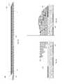
- FIG. 10Ais an elevational view of part of a tiered offset stacked die assembly mounted on a support, showing electrical connection of the lower tier to the support.
- FIG. 10Bis a plan view of part of a lower tier of a tiered offset stacked die assembly mounted on a support, showing electrical connection of the lower tier to the support.
- FIG. 11Ais an elevational view of part of a tiered offset stacked die assembly mounted on a support, showing electrical connection of the upper tier to the support.
- FIG. 11Bis a plan view of part of a tiered offset stacked die assembly mounted on a support, showing electrical connection of the upper tier to the support.
- FIG. 12Ais an elevational view of part of a tiered offset stacked die assembly mounted on a support, showing a stage in a process for forming electrical connection of the upper tier to the support.
- FIG. 12Bis a plan view of part of a tiered offset stacked die assembly mounted on a support as in FIG. 12A , showing an electrical connection of the upper tier to the support.
- FIG. 12Cis a plan view of part of a tiered offset stacked die assembly mounted on a support as in FIG. 12A , showing a stage in a process for forming electrical connection of the upper tier to the support.
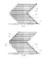
- FIG. 1Ashows in a plan view an arrangement of offset stacked die 10 mounted on a support, each die having interconnect pads arranged in one margin adjacent a front die edge; and FIG. 1B shows the stack mounted on the support in a sectional view as indicated at 1 B- 1 B in FIG. 1A .
- the stackincludes seven die 141 , 142 , 143 , 144 , 145 , 146 , 147 , each mounted with the active side of the die facing away from the support 17 .
- interconnect pads 148are in this example situated in a row 142 alongside a front die edge 149 .
- the die 147 in this exampleis covered on all surfaces (back surface, front surface, sidewalls) by an electrically insulative conformal coating 144 , provided with openings 145 exposing interconnect pads 148 .
- Successive coated die in the stackmay, as in these examples, rest directly one upon another, such that the coating on the back side of an upper die can contact the coating on the front side of the underlying die.
- the conformal coatingmay cover fewer than all the die surfaces, or it may cover only parts of one or more die surfaces; generally, the electrically insulative conformal coating may be formed at least over surfaces or features that require electrical insulation from other features or surfaces that they may contact in the completed assembly.
- a die attach filmmay be laminated onto the back side of one or more of the die.
- each diehas interconnect pads situated in a margin along one front die edge (an “interconnect” edge), and succeeding die in the stack are arranged so that their respective interconnect edges face toward the same face of the stack. Successive die in the stack are displaced (offset) in a direction orthogonal to the die edge along which the pads are situated, and in the example shown here the offset leaves the pads in each underlying die fully exposed.
- This configurationpresents as a stairstep die stack, and electrical interconnections are made over the steps.
- the stackis mounted on a support 17 (for example, a package substrate) having a row 173 of bond sites 172 exposed at a die mount surface 171 .
- the bond sitesare connected to (or constitute a part of) electrical circuitry (not shown in the FIGs.) in the support.
- the die stackis affixed to the die mount surface 171 of the substrate, and arranged so that the front sidewall of the first (lowermost) die 141 is aligned along the row 173 of bond sites 172 .
- the front sidewall of the lowermost dieoverlaps the bond sites to a small extent; in other examples, the front sidewall of the lowermost die may be set back from the row of bond sites, or may overlap the bond sites to a greater extent.
- the coated back side of the first diemay, as in these examples, directly contact the support surface 171 and may serve to affix the stack to the support.
- a die attach filmmay be laminated onto the back side of the first die to serve to affix the stack to the support.
- the dieare electrically interconnected (die-to-die) in the stack, and the stack is electrically connected to the support, by traces 174 of an interconnect material disposed in contact with die pads, e.g. 148 , and bond pads 172 , as shown in FIG. 1C .
- the interconnect materialmay be an electrically conductive polymer, such as a polymer matrix containing particles of an electrically conductive material.
- the materialmay be a curable material, such as a curable polymer, for example, such as electrically conductive epoxy (for example, a silver filled epoxy); and the interconnection may be made by forming traces of the uncured material in a prescribed pattern and thereafter curing the material to secure the electrical contacts with the die pads and the bond sites, and to ensure the mechanical integrity of the traces between them.
- the materialmay be an electrically conductive ink, which may include electrically conductive particles in a carrier, and which may or may not include a polymer matrix.
- larger stacked die assembliesmay be made by constructing offset stacked die units in a modular design, and then stacking the units.
- One such modular unitmay be inverted and mounted over another, with the interconnect ends of the respective modular units aligned and connected; the resulting two-tiered assembly presents a zig-zag configuration, as illustrated for example in FIGS. 2A , 2 B.
- a first offset die stackconstitutes a first modular unit (a first tier) 210 , which may be mounted onto and electrically connected to bond pads 272 on a support 217 ; and a second similar modular unit (a second tier) 212 may be inverted and mounted over the first tier 210 , with the ends of the interconnects 214 , 224 of the respective modular units aligned and connected.
- a resulting assemblyis shown by way of example in FIG. 2A .
- a spacermay be provided (not shown in FIG. 2A ) between the first and second tiers.
- FIG. 2Bshows a configuration in which a second tier is mounted over a first tier, but is not inverted.
- An interposerincluding at least one dielectric layer 216 (such as glass, for example) and at least one patterned conductive layer 244 is situated between the modular units, to provide rerouting from the ends of the interconnects 214 on one edge of the first tier 210 to the ends of the interconnects 224 on the (oppositely situated) edge of the second tier 220 .
- Rheological propertiessuch as viscosity, or thixotropy, for example
- a portion of a deposit massmay remain in contact with the deposition tool for a time following completion of a dispense pulse, and the tool may be moved before separation is complete.
- a conductive polymer material having higher viscosity and thixotropy in the uncured statecan be shaped during deposition by moving the deposition tool immediately following a dispense pulse, to draw a “tail” of material in a selected direction to form an interconnect having a selected shape.
- the shape of the deposited massmay be determined to some degree by the direction and rate of movement of the tool as well as the rheologic properties of the material.
- the offset die stacks in the examples shown in FIGS. 1A , 1 B, 1 C, 2 A and 2 Bare shown as having seven die. Offset stacks having other number of die are contemplated and, typically, an even number of die (for example, four die or eight die per offset stack) may be more usual.
- a droplet 304is shown attached to an electrical contact 328 on a support 320 (such as a pad on a die, or a bond pad on a substrate).
- a support 320such as a pad on a die, or a bond pad on a substrate.
- the tool tip(not shown in the FIG.) was directed toward the contact 328 , and a mass of material was dispensed onto the contact. Then, while the mass of material was still in contact with the tool tip, the tool was moved perpendicularly away from the target to draw a “tail” of material upward.
- the droplet mass separated from the tool tip, and the resulting droplet 304has a generally conical shape.
- Materials suitable for forming shaped dropletsinclude electrically conductive epoxies (metal-filled epoxies) having, in the uncured state, a viscosity about 30,000 cps or greater and/or a thixotropic index about 6.5 or greater.
- electrically conductive epoxiesmetal-filled epoxies
- a viscosityabout 30,000 cps or greater
- a thixotropic indexabout 6.5 or greater.
- the viscosity and/or thixotropymust not be too high, or else the material may be unworkable, or it may not make good contact with the interconnect terminals.
- die stackshaving a number of die mounted over one another and separated by spacers; or by a staggered arrangement of die (that is, where the space between the die to be connected approximates (or somewhat exceeds) the thickness of an interposed offset die; or in die stacks having elongated stacked die each oriented 90° to the die below, as described in U.S. application Ser. No. 12/124,077, referenced above and incorporated by reference herein.
- an offset stack of die 341 , 342 , 343 , 344is shown mounted on a substrate 317 having an electrical connection site (such as a bond pad) 372 in the stack mount side. All the die in this example have peripheral pads, e.g., 348 , arranged in an interconnect margin along an edge of the die. Each die in the stack is displaced with respect to the die beneath, to expose at least a portion of the area of the pads (exposing the entirety of the pads in the example shown).
- a first interconnect droplet 314is shown connecting the die pad 348 on the first die 341 to the bond pad 372 in the substrate 317 .
- the toolwas directed toward the first target bond pad 372 , and a mass of material was dispensed onto the bond pad. Then, while the mass of material was still in contact with the tool tip, the tool was moved, first upwardly and laterally away from the first target and then downwardly and laterally toward the die pad 348 (as indicated by the broken arrow) to draw a “tail” of material in an arc toward the second pad.
- Second and subsequent dropletscan be similarly formed to connect pads on the successive die, forming a die-to-die interconnection.
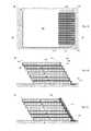
- FIGS. 4A , 4 B and 4 CA tiered offset stacked die assembly in a zig-zag configuration, mounted on and electrically connected to a support according to an embodiment of the invention is shown in FIGS. 4A , 4 B and 4 C.
- a stacked die assembly 428including two tiers each having four offset stacked die, is mounted on a support (such as a package substrate) 447 .
- the lower tierincludes die 441 , 442 , 443 , 444 ; and the upper tier includes die 445 , 446 , 447 , 448 .
- each dieis laminated with a die attach film (respectively, 431 , 432 , 433 , 434 , 435 , 436 , 437 , 438 ).
- Interconnect die padse.g., 548 ; 648
- Traces 404 of an interconnect materialare formed over the interconnect face of the first tier, contacting interconnect die pads (e.g., 548 ) to make die-to-die interconnection, and contacting bond pads 472 in a first row on the support to make tier-to-support electrical connection.
- Pedestals 502 of an interconnect materialare formed in contact with bond pads 474 in a second row on the support; and traces 504 of an interconnect material are formed over the interconnect face of the second tier, contacting interconnect die pads (e.g., 648 ) to make die-to-die interconnection, and contacting pedestals 502 to make tier-to-support electrical connection.
- interconnect die padse.g., 648
- the substrate 477includes lands 476 at a surface opposite the stack mount surface, for second-level electrical connection (for example as a land grid array or a ball grid array or a tab array) of the assembly to underlying circuitry in a device (not shown in these FIGs.) in which the assembly is deployed for use.
- the bond pads 472 , 474 and the lands 476are connected to (or constitute parts of) patterned conductive layers, separated by one or more dielectric layers, in the substrate, and the patterned conductive layers in the substrate are connected by vias through the dielectric layer or layers.
- a description of such a processfollows.
- semiconductor circuitry for an array of dieis formed in an active side (front side) of a semiconductor wafer.
- the waferis thinned, typically by backgrinding, and a die attach film is mounted onto the back side of the thinned wafer.
- the dieare singulated by cutting (for example, by sawing) along the saw streets between the die in the array.
- the singulated dieare stacked, using a tool such as a pick-and-place tool, in the offset arrangement.
- a first offset stack of diein this example, four die constituting a first tier 420 is mounted onto a stack mount surface of the substrate 477 .
- the first tieris situated so that the die attach sidewall of the lowermost die 441 is aligned with (adjacent to, or partially overlapping) the bond pads 472 in the first bond pad row on the substrate.
- the assemblyis coated with a dielectric coating 544 .
- the material of the dielectric coatingmay be any of a variety of materials, and may be formed using any of a variety of techniques as appropriate for the particular material.
- Suitable materialsinclude organic polymers, and particularly suitable materials include parylenes, which are formed by in situ polymerization of precursor molecules in vapor form.
- the coatingcovers all surfaces that are exposed to the material during the coating process, including areas where electrical connection is to be made. Accordingly, openings are formed over selected areas, for example by selective laser ablation. For example, openings 545 are formed through the coating to expose interconnect die pads (e.g., 548 ) and to expose bond pads (e.g., 472 ) in the first row on the substrate.
- a resulting constructis shown in FIG. 5A , and in partial views, enlarged, in FIGS. 5B , 5 C.
- Interconnection of the die in the first tier 420 and connection of the first tier to the substrateis thereafter made by forming traces 404 of an electrically conductive material in contact with interconnect die pads and with the bond pads 472 .
- a resulting constructis shown in FIG. 6A , and in partial views, enlarged, in FIGS. 6B , 6 C.
- the dielectric coatingserves to insulate features that may be contacted by the electrically conductive traces, but to which electrical contact is not desired, such as the die margins along which the die pads are situated, and the adjacent die edges and sidewalls.
- the electrically conductive materialincludes materials that can be deposited in a flowable form and thereafter hardened or allowed to harden to form the conductor.
- the electrically conductive materialmay be a curable material, and may be deposited in an uncured or partially cured state; and the material may be partially or additionally cured at an intermediate stage following deposition, and may be fully cured when deposition has been completed.
- Suitable electrically conductive materialsinclude polymers filled with a conductive material in particle form such as, for example, metal-filled polymers, including, for example metal filled epoxy, metal filled thermosetting polymers, metal filled thermoplastic polymers, and electrically conductive inks.
- the interconnect materialmay be deposited by any technique suitable for the particular material.
- the materialmay be dispensed using a nozzle or needle, or sprayed as an aerosol, or screen printed, or jet printed; the material may be continuously dispensed or dispensed in pulses, as for example dropwise through a jet or nozzle. Following dispense, the material is cured to complete the interconnection.
- a second offset stack of die(four die in this example) constituting a second tier 422 is mounted onto the upper surface of the first tier 420 .
- the second tieris situated in this example so that the die attach sidewall of the lowermost die 445 overhangs the first tier, and is vertically aligned in relation to the bond pads 474 in the second bond pad row on the substrate.
- the resulting assemblyis thereafter coated with a second dielectric coating 644 .
- the material of the second dielectric coatingmay be any of a variety of materials, and may be formed using any of a variety of techniques as appropriate for the particular material.
- the second coating materialmay be the same as, or different from, the first coating material.
- Suitable materialsinclude organic polymers, and particularly suitable materials include parylenes, which are formed by in situ polymerization of precursor molecules in vapor form.
- the coatingcovers all surfaces that are exposed to the material during the coating process, including areas where electrical connection is to be made. Accordingly, openings are formed over selected areas, for example by selective laser ablation. For example, openings 645 are formed through the coating to expose interconnect die pads (e.g., 648 ) and to expose bond pads (e.g., 474 ) in the second row on the substrate.
- a resulting constructis shown in FIG. 7A , and in partial views, enlarged, in FIGS. 7B , 7 C.
- the electrically conductive materialincludes materials that can be deposited in a flowable form and thereafter hardened or allowed to harden to form the conductor.
- the electrically conductive materialmay be a curable material, and may be deposited in an uncured or partially cured state; and the material may be partially or additionally cured at an intermediate stage following deposition, and may be fully cured when deposition has been completed.
- Suitable electrically conductive materialsinclude polymers filled with a conductive material in particle form such as, for example, metal-filled polymers, including, for example metal filled epoxy, metal filled thermosetting polymers, metal filled thermoplastic polymers, and electrically conductive inks.
- Suitable materialsare selected as having rheological properties suitable to maintain the pedestal height and general shape as dispensed and prior to final cure.
- the pedestalshave a generally conical shape, having a height in a range about 190-310 um, and a base diameter in a range about 160-180 um, for example. Pedestals having greater height-to-diameter proportions may be made, depending upon the properties of the materials.
- An epoxy “bleed” surrounding the base, as illustrated at 512 in FIG. 8Bmay result during the deposition and cure process; in some embodiments this may not be a desirable feature.
- suitable materials for the conductive pedestalsinclude the electrically conductive pastes marketed as the “800, 700, 500, 400, 200 series inks” by Ormet Circuits, Inc. These include 5-15 wt % of an epoxy resin mixture, and up to 5 wt % of butyl carbitol; with the remainder including various proportions of particles of Cu, Bi, Sn and Ag.
- suitable materials for the conductive pedestalsinclude materials marketed as “die attach adhesives” by Lord Corporation, such as the “Thermoset MD-141”. These include about 10 wt % of a phenolic novolac resin, about 5 wt % of a glycol ether compound, about 10 wt % of an epoxy resin, and about 80 wt % of silver.
- the interconnect material for the pedestalsmay be deposited by any technique suitable for the particular material and pedestal shape.
- the materialmay be dispensed using a nozzle or needle or screen printed, or jet printed; the material may be continuously dispensed or dispensed in pulses, as for example dropwise through a jet or nozzle. Following dispense the material of the pedestals is cured to complete the mechanical integrity of the pedestals.
- interconnection of the die in the second tier 422 and connection of the second tier to the substrateis made by forming traces 504 of an electrically conductive material in contact with interconnect die pads and with the pedestals 502 .
- a resulting constructis shown in FIG. 9A , and in partial views, enlarged, in FIGS. 9B , 9 C.
- the dielectric coatingserves to insulate features that may be contacted by the electrically conductive traces, but to which electrical contact is not desired, such as the die margins along which the die pads are situated, and the adjacent die edges and sidewalls.
- the electrically conductive materialincludes materials that can be deposited in a flowable form and thereafter hardened or allowed to harden to form the conductor.
- the electrically conductive materialmay be a curable material, and may be deposited in an uncured or partially cured state; and the material may be partially or additionally cured at an intermediate stage following deposition, and may be fully cured when deposition has been completed.
- Suitable electrically conductive materialsinclude polymers filled with a conductive material in particle form such as, for example, metal-filled polymers, including, for example metal filled epoxy, metal filled thermosetting polymers, metal filled thermoplastic polymers, and electrically conductive inks. Suitable materials are selected as having rheological properties suitable to maintain its shape spanning the gap between the sidewall of the die 445 and the tip of the pedestal, following dispense and prior to final cure.
- the interconnect materialmay be deposited by any technique suitable for the particular material.
- the materialmay be dispensed using a nozzle or needle, or sprayed as an aerosol, or screen printed, or jet printed; the material may be continuously dispensed or dispensed in pulses, as for example dropwise through a jet or nozzle.
- FIGS. 10A and 10Bare partial views showing the conductive traces 404 making die-to-die interconnection of the die in the first tier 420 , and connection of the first tier 420 to the bond pads 472 on the substrate.
- FIGS. 11A and 11Bare partial views showing the conductive traces 504 making die-to-die interconnection of the die in the second tier 422 , and connection of the second tier 422 to the pedestals 502 on the substrate.
- FIGS. 12A , 12 B, 12 Care partial views showing stages in the formation of the conductive traces 504 making die-to-die interconnection of the die in the second tier 422 , and connection of the first tier 422 to the pedestals 502 on the bond pads 474 on the substrate.
- the drawingsshow assemblies in which a tiered die stack (the upper offset die stack in these examples) is elevated over the support; and the pillars are deployed for electrical connection of an elevated offset die stack to bond pads on the support. In other contemplated embodiments the pillars are deployed for electrical connection of an elevated die or die stack (offset or not) to bond pads on the support.
- the drawingsshow assemblies in which a lower offset die stack is situated between the upper stack and the support. Particularly, in the illustrated examples a lower offset die stack is mounted onto the support, and the upper stack is mounted on the lower stack, so that the elevation of the upper stack is imposed by the height of the lower stack over the substrate surface (or the height of the lower stack). In other contemplated embodiments the upper stack may be mounted over some feature other than a lower stack, such as, for example, a lower die or a lower non-offset die stack, or a package.
- the illustrated zig-zag tiered die stack assemblieshave two tiers (lower and upper), and each tier is shown as having four die. Assemblies having more than two tiers are contemplated, and tiers having other numbers of die are contemplated. For example, one or more additional tiers may be stacked over the second tier. And, for example, one or more of the tiers may have more or fewer than four die and, in some embodiments, one or more tiers may have eight die, for example.
- the die in the upper and lower tiersare shown as having the same length. This circumstance may prevail where, for example, all the die are of the same type or have the same functionality.
- Each of the tiered stacksmay, for example, include memory die of the same type.
- Other die typesare contemplated. For example, die having different functionalities may be included within a tier; or, for example, the die in one tier may have the same functionality, while the die in another tier may have one or more different functionalities. Consequently, in some contemplated embodiments the die may not be the same size; or the die in one tier may be the same size, while die in another tier may have different dimensions.
- the interconnect edge of the lowermost die in the upper tieris shown in the examples as extending outward beyond the underlying edge of the lower feature (that is, beyond the underlying die edge of the uppermost die in the lower tier in the examples shown).
- the interconnect edge of the upper stackmay be vertically aligned with, or may lie inwardly from, the underlying edge of the lower feature.
- the dielectric coatingis shown as being removed from interconnect pads on all the die in the stacks. This allows contact of all the pads to a subsequently-formed trace. It may be desirable to form electrical connection with only selected ones of the pads. As illustrated and discussed in U.S. application Ser. No. 12/124,077, referenced above and incorporated by reference herein, openings may be formed over selected ones of the pads in any die, or selected corresponding pads on successive die in the stack, leaving the remaining pads covered by the dielectric coating and unavailable for electrical connection. And, for example the coating is described as being formed in phases, with each phase following construction of each of the tiers. In some contemplated embodiments the coating is applied in a single phase following formation of two (or more). This may be particularly desirable where an upper tier is situated over a lower tier such that the interconnect die pads in the lower tier are readily available for removal (as for example, by laser ablation).
- each pillar and corresponding tracemay be formed in a continuous operation, by suitable control of the dispense and of the dispense tool.
Landscapes
- Engineering & Computer Science (AREA)
- Microelectronics & Electronic Packaging (AREA)
- Power Engineering (AREA)
- Computer Hardware Design (AREA)
- Physics & Mathematics (AREA)
- Condensed Matter Physics & Semiconductors (AREA)
- General Physics & Mathematics (AREA)
- Manufacturing & Machinery (AREA)
- Encapsulation Of And Coatings For Semiconductor Or Solid State Devices (AREA)
- Combinations Of Printed Boards (AREA)
- Wire Bonding (AREA)
- Lead Frames For Integrated Circuits (AREA)
Abstract
Description
- This application claims priority from R. Co et al. U.S. Provisional Application No. 61/220,986, titled “Electrical interconnect for die stacked in zig-zag configuration”, which was filed Jun. 26, 2009, and which is hereby incorporated by reference herein.
- This invention relates to electrical interconnection of integrated circuit chips and, particularly, to electrical interconnection of stacked die.
- A typical semiconductor die has a front (“active”) side, in which the integrated circuitry is formed, a back side, and sidewalls. The sidewalls meet the front side at front edges and the back side at back edges. Semiconductor die typically are provided with interconnect pads (die pads) located at the front side for electrical interconnection of the circuitry on the die with other circuitry in the device in which the die is deployed. Typically, the die pads consist of an electrically conductive metal or metallization, such as copper or aluminum.
- Some die as provided have die pads on the front side along one or more of the die margins, and these may be referred to as peripheral pad die. Other die as provided have die pads arranged in one or two rows on the front side near the center of the die, and these may be referred to as center pad die. Some die have pads arranged in an area array. However the die pads may be arranged in the die as provided, the die may be “rerouted” to provide a suitable arrangement of interconnect pads at or near one or more of the margins of the die.
- A number of approaches have been proposed for increasing the density of active semiconductor circuitry in integrated circuit chip packages, while minimizing package size (package footprint, package thickness). In one approach to making a high density package having a smaller footprint, two or more semiconductor die, of the same or different functionality, are stacked one over another and mounted on a package substrate.
- S. McElrea et al. U.S. application Ser. No. 12/124,077, filed May 20, 2008, titled “Electrically interconnected stacked die assemblies” describes stacked die configurations in which interconnect pads on the die are electrically connected by traces of an electrically conductive interconnect material. In some configurations adjacent die in the stack are provided with interconnect pads arranged at the front side along a die margin, and the edge at the margin of an overlying die is offset in relation to the margin of the die beneath it. The offset reveals at least a fraction of the area of the interconnect pads on the lower die, so that the pads on the lower die are available for electrical connection with pads on a die situated above. The electrically conductive interconnect material is an electrically conductive polymer, such as a curable conductive epoxy, for example. Larger stacked die assemblies may be made by constructing offset stacked die units in a modular design, and then stacking the units. One such modular unit may be inverted and mounted over another, with the interconnect ends of the respective modular units aligned and connected; the resulting two-tiered assembly presents a zig-zag configuration.
- T. Caskey et al. U.S. application Ser. No. 12/124,097, filed May 20, 2008, titled “Electrical interconnect formed by pulse dispense” describes methods for electrical interconnection of die in a stack, and of stacked die with a substrate, by depositing an electrical interconnect material in situ in a series of pulses to form an electrically continuous interconnection. The interconnect material may be a curable material, and may be deposited in an uncured or partially cured state; and the material may be partially or additionally cured at an intermediate stage following dispense, and may be fully cured when dispense has been completed. Suitable interconnect materials include polymers filled with conductive material in particle form such as, for example, metal-filled polymers, including, for example metal filled epoxy, metal filled thermosetting polymers, metal filled thermoplastic polymers, or electrically conductive inks.
- In a general aspect the invention features a die (or of a stack of die) mounted over and elevated above a support, and electrically connected to circuitry in the support. Pillars of electrically conductive material are formed on a set of bond pads at a mount side of the support, and the elevated die (or at least one die in the elevated stack of die) is electrically connected to the support, by traces of an electrically conductive material contacting interconnect pads on the die to the pillars, and through the pillars to the support.
- In some embodiments a lower die, or a lower stack of die, or a semiconductor package, is situated between the support and the elevated die; and in some embodiments the lower die or stack of die, or package, is electrically connected to the support. In some embodiments the lower stack of die is a lower tiered offset stacked die assembly, and die in the first tier are electrically interconnected die-to-die, and the lower tier is electrically connected to a support, by traces of an electrically conductive material contacting interconnect pads on the die and a set of bond pads on the support.
- In some embodiments the elevated stack of die is a tiered offset stacked die assembly, in which the interconnect edges of the tier of die face in a first direction, and the interconnect die pads are aligned with the pillars.
- In various embodiments the invention features tiered offset stacked die assemblies in a zig-zag configuration, in which the interconnect edges of a first (lower) tier face in a first direction, and the interconnect edges of a second (upper) tier, stacked over the first tier, face in a second direction, different from the first direction. The second tier interconnect edge direction may be opposite to or orthogonal to the first tier interconnect edge direction. Die in the first tier are electrically interconnected die-to-die, and the tier is electrically connected to a support, by traces of an electrically conductive material contacting interconnect pads on the die and a first set of bond pads on the support. Pillars of a electrically conductive material are formed on a second set of bond pads, and die in the second tier are electrically interconnected die-to-die, and the tier is electrically connected to the support, by traces of an electrically conductive material contacting interconnect pads on the die to the pillars, and through the pillars to the substrate.
- The electrically conductive material includes particles of a metal in a polymer matrix. Suitable materials include materials that can be deposited in a flowable form and thereafter hardened or allowed to harden to form the conductor. The interconnect material may be a curable material, and may be deposited in an uncured or partially cured state; and the material may be partially or additionally cured at an intermediate stage following deposition, and may be fully cured when deposition has been completed. Suitable interconnect materials include polymers filled with conductive material in particle form such as, for example, metal-filled polymers, including, for example metal filled epoxy, metal filled thermosetting polymers, metal filled thermoplastic polymers; and electrically conductive inks.
- The interconnect material may be deposited by any technique suitable for the particular material. In some embodiments the material may be dispensed using a nozzle or needle, or sprayed as an aerosol, or screen printed, or jet printed; the material may be continuously dispensed or dispensed in pulses, as for example dropwise through a jet or nozzle.
- In another general aspect the invention features a method for electrically connecting a die (or of a stack of die), mounted over and elevated above a support, to circuitry in the support, by: forming pillars of electrically conductive material on a set of bond pads at a mount side of the support, and forming traces of an electrically conductive material, each trace in contact with an interconnect die pad on the elevated die (or on at least one die in the elevated stack of die) and with a pillar. In some embodiments the traces span a gap between the pillars and the interconnect die pads. In some embodiments forming the pillars includes depositing a curable electrically conductive pillar material on a bond pad and curing the deposited pillar material. In some embodiments forming the traces includes depositing a curable electrically conductive trace material in contact with a pillar and curing the deposited trace material. In some embodiments the pillar and trace are formed in a continuous operation.
- In another general aspect the invention features a method for making a tiered offset stacked die assembly in a zig-zag configuration, by: stacking or mounting a first (lower) tier on a support, arranged so that the interconnect edges of the first (lower) tier face in a first direction and so that interconnect pads on at least a lowermost die in the first tier are aligned with a first set of bond pads on the support; electrically interconnecting die in the first tier die-to-die, and electrically connecting the tier to the support, by forming first tier traces of an electrically conductive material each in contact with at least one interconnect pad on the die and with one of said first set of bond pads; stacking or mounting a second (upper) tier over the first tier, arranged so that the interconnect edges of the second (upper) tier face in a second direction; forming pillars of electrically conductive material on a second set of bond pads on the support; and forming second tier traces of an electrically conductive material, each trace in contact with an interconnect die pad on at least one die in the second (upper) tier and with a pillar. In some embodiments forming the first tier traces includes depositing a curable electrically conductive trace material in contact with a die pad on at least one lower tier die and with one of a first set of bond pads, and curing the deposited trace material. In some embodiments forming the second tier traces includes forming the traces across a gap between the pillars and the interconnect die pads. In some embodiments forming the pillars includes depositing a curable electrically conductive pillar material on a bond pad and curing the deposited pillar material. In some embodiments forming the second tier traces includes depositing a curable electrically conductive trace material in contact with a die pad on at least one upper tier die and with a pillar, and curing the deposited trace material. The pillars, the first tier traces, and the second tier traces may be formed of the same or of different materials. In embodiments in which the pillars and the second tier traces are formed of the same material, the pillar and trace may be formed separately, or may be formed in a continuous operation.
- In some embodiments the method for making a tiered offset stacked die assembly includes, following stacking or mounting the first tier and prior to forming first tier traces, coating the assembly with a conformal dielectric coating and forming openings in at least selected die pads and bond pads to be contacted with the first tier traces. In some embodiments the method for making a tiered offset stacked die assembly includes, following stacking or mounting the second tier and prior to forming the pillars, coating the assembly with a conformal dielectric coating and forming openings in at least selected second tier die pads and bond pads to be contacted with the pillars.
FIGS. 1A and 1B are diagrammatic sketches showing an offset die stack mounted on a support, in plan view (FIG. 1A ) and in a sectional view (FIG. 1B ).FIG. 1C is a diagrammatic sketch in a sectional view showing an offset die stack mounted on a support, as inFIG. 1B , in which the die are electrically interconnected die-to-die and the die stack electrically connected to the support.FIGS. 2A and 2B are diagrammatic sketches in sectional view showing two stacked die units mounted one over another in a zig-zag configuration.FIG. 3A is a diagrammatic sketch showing a free standing droplet of curable interconnect material, andFIG. 3B is a diagrammatic sketch showing a stage in a process for forming electrical interconnects between a die and a support.FIGS. 4A ,4B and4C are diagrammatic sketches in sectional view showing a tiered offset stacked die assembly in a zig-zag configuration, mounted on and electrically connected to a support.FIGS. 5A ,5B and5C;6A,6B and6C;7A,7B and7C;8A,8B and8C; and9A,9B and9C are diagrammatic sketches in sectional view showing stages in a process for constructing a tiered offset stacked die assembly in a zig-zag configuration, mounted on and electrically connected to a support, as inFIGS. 4A ,4B and4C.FIGS. 4B ,5B,6B,7B,8B and9B are part-sectional views as indicated at B inFIGS. 4A ,5A,6A,7A,8A,9A, respectively; andFIGS. 4C ,5C,6C,7C,8C and9C are part-sectional views as indicated at C inFIGS. 4A ,5A,6A,7A,8A,9A, respectively.FIG. 10A is an elevational view of part of a tiered offset stacked die assembly mounted on a support, showing electrical connection of the lower tier to the support.FIG. 10B is a plan view of part of a lower tier of a tiered offset stacked die assembly mounted on a support, showing electrical connection of the lower tier to the support.FIG. 11A is an elevational view of part of a tiered offset stacked die assembly mounted on a support, showing electrical connection of the upper tier to the support.FIG. 11B is a plan view of part of a tiered offset stacked die assembly mounted on a support, showing electrical connection of the upper tier to the support.FIG. 12A is an elevational view of part of a tiered offset stacked die assembly mounted on a support, showing a stage in a process for forming electrical connection of the upper tier to the support.FIG. 12B is a plan view of part of a tiered offset stacked die assembly mounted on a support as inFIG. 12A , showing an electrical connection of the upper tier to the support.FIG. 12C is a plan view of part of a tiered offset stacked die assembly mounted on a support as inFIG. 12A , showing a stage in a process for forming electrical connection of the upper tier to the support.- The invention will now be described in further detail by reference to the drawings, which illustrate alternative embodiments of the invention. The drawings are diagrammatic, showing features of the invention and their relation to other features and structures, and are not made to scale. For improved clarity of presentation, in the FIGs. illustrating embodiments of the invention, elements corresponding to elements shown in other drawings are not all particularly renumbered, although they are all readily identifiable in all the FIGs. Also for clarity of presentation certain features are not shown in the FIGs., where not necessary for an understanding of the invention. At some points in the description, terms of relative positions such as “above”, “below”, “upper”, “lower”, “top”, “bottom” and the like may be used, with reference to the orientation of the views in the drawings; such terms are not intended to limit the orientation of the device in use.
FIG. 1A shows in a plan view an arrangement of offsetstacked die 10 mounted on a support, each die having interconnect pads arranged in one margin adjacent a front die edge; andFIG. 1B shows the stack mounted on the support in a sectional view as indicated at1B-1B inFIG. 1A . In this example the stack includes sevendie support 17. Referring to the uppermost die147 in the stack, for example,interconnect pads 148 are in this example situated in arow 142 alongside afront die edge 149. Thedie 147 in this example is covered on all surfaces (back surface, front surface, sidewalls) by an electrically insulativeconformal coating 144, provided withopenings 145 exposinginterconnect pads 148. Successive coated die in the stack may, as in these examples, rest directly one upon another, such that the coating on the back side of an upper die can contact the coating on the front side of the underlying die. In other examples, the conformal coating may cover fewer than all the die surfaces, or it may cover only parts of one or more die surfaces; generally, the electrically insulative conformal coating may be formed at least over surfaces or features that require electrical insulation from other features or surfaces that they may contact in the completed assembly. Optionally, or additionally, a die attach film may be laminated onto the back side of one or more of the die.- In the example shown in
FIGS. 1A and 1B each die has interconnect pads situated in a margin along one front die edge (an “interconnect” edge), and succeeding die in the stack are arranged so that their respective interconnect edges face toward the same face of the stack. Successive die in the stack are displaced (offset) in a direction orthogonal to the die edge along which the pads are situated, and in the example shown here the offset leaves the pads in each underlying die fully exposed. This configuration presents as a stairstep die stack, and electrical interconnections are made over the steps. - The stack is mounted on a support17 (for example, a package substrate) having a
row 173 ofbond sites 172 exposed at adie mount surface 171. The bond sites are connected to (or constitute a part of) electrical circuitry (not shown in the FIGs.) in the support. The die stack is affixed to thedie mount surface 171 of the substrate, and arranged so that the front sidewall of the first (lowermost) die141 is aligned along therow 173 ofbond sites 172. In the example illustrated here, the front sidewall of the lowermost die overlaps the bond sites to a small extent; in other examples, the front sidewall of the lowermost die may be set back from the row of bond sites, or may overlap the bond sites to a greater extent. The coated back side of the first die may, as in these examples, directly contact thesupport surface 171 and may serve to affix the stack to the support. Optionally, a die attach film may be laminated onto the back side of the first die to serve to affix the stack to the support. - The die are electrically interconnected (die-to-die) in the stack, and the stack is electrically connected to the support, by
traces 174 of an interconnect material disposed in contact with die pads, e.g.148, andbond pads 172, as shown inFIG. 1C . The interconnect material may be an electrically conductive polymer, such as a polymer matrix containing particles of an electrically conductive material. The material may be a curable material, such as a curable polymer, for example, such as electrically conductive epoxy (for example, a silver filled epoxy); and the interconnection may be made by forming traces of the uncured material in a prescribed pattern and thereafter curing the material to secure the electrical contacts with the die pads and the bond sites, and to ensure the mechanical integrity of the traces between them. The material may be an electrically conductive ink, which may include electrically conductive particles in a carrier, and which may or may not include a polymer matrix. - As described in U.S. application Ser. No. 12/124,077, larger stacked die assemblies may be made by constructing offset stacked die units in a modular design, and then stacking the units. One such modular unit may be inverted and mounted over another, with the interconnect ends of the respective modular units aligned and connected; the resulting two-tiered assembly presents a zig-zag configuration, as illustrated for example in
FIGS. 2A ,2B. A first offset die stack constitutes a first modular unit (a first tier)210, which may be mounted onto and electrically connected to bondpads 272 on asupport 217; and a second similar modular unit (a second tier)212 may be inverted and mounted over thefirst tier 210, with the ends of theinterconnects FIG. 2A . A spacer may be provided (not shown inFIG. 2A ) between the first and second tiers. As may be appreciated, where the first and second modular units are identical, when the second unit is inverted the respective rows of pads at the interconnect ends are antiparallel; that is, a first interconnect on the first unit is now aligned with a last interconnect on the second die. In such configurations, rerouting circuitry may be required, to connect the appropriate respective features on the die. Rerouting circuitry may be provided at the active side of the top die of the first unit; or, where a spacer is included, the spacer may constitute an interposer (not shown inFIG. 2A ), including one or more dielectric layers and one or more conductive rerouting layers.FIG. 2B shows a configuration in which a second tier is mounted over a first tier, but is not inverted. Here the ends of theinterconnects 224 of thesecond tier 220 are near the opposite edge of the top die in thefirst tier 210. An interposer, including at least one dielectric layer216 (such as glass, for example) and at least one patternedconductive layer 244 is situated between the modular units, to provide rerouting from the ends of theinterconnects 214 on one edge of thefirst tier 210 to the ends of theinterconnects 224 on the (oppositely situated) edge of thesecond tier 220. - Rheological properties (such as viscosity, or thixotropy, for example) of particular interconnect materials may be exploited to provide deposits having controlled shapes. Particularly, for some materials a portion of a deposit mass may remain in contact with the deposition tool for a time following completion of a dispense pulse, and the tool may be moved before separation is complete. A conductive polymer material having higher viscosity and thixotropy in the uncured state can be shaped during deposition by moving the deposition tool immediately following a dispense pulse, to draw a “tail” of material in a selected direction to form an interconnect having a selected shape. As a result, the shape of the deposited mass may be determined to some degree by the direction and rate of movement of the tool as well as the rheologic properties of the material.
- As noted above, the offset die stacks in the examples shown in
FIGS. 1A ,1B,1C,2A and2B are shown as having seven die. Offset stacks having other number of die are contemplated and, typically, an even number of die (for example, four die or eight die per offset stack) may be more usual. - Referring to
FIG. 3A , for example, adroplet 304 is shown attached to anelectrical contact 328 on a support320 (such as a pad on a die, or a bond pad on a substrate). In the example shown, during formation of the droplet, the tool tip (not shown in the FIG.) was directed toward thecontact 328, and a mass of material was dispensed onto the contact. Then, while the mass of material was still in contact with the tool tip, the tool was moved perpendicularly away from the target to draw a “tail” of material upward. Eventually the droplet mass separated from the tool tip, and the resultingdroplet 304 has a generally conical shape. Materials suitable for forming shaped droplets include electrically conductive epoxies (metal-filled epoxies) having, in the uncured state, a viscosity about 30,000 cps or greater and/or a thixotropic index about 6.5 or greater. As will be appreciated, the viscosity and/or thixotropy must not be too high, or else the material may be unworkable, or it may not make good contact with the interconnect terminals. - U.S. application Ser. No. 12/124,097, referenced above and incorporated by reference herein, describes forming a series of such roughly conical free standing droplets one over another adjacent a die stack face, providing a column of material contacting the interconnect terminals. Such a columnar configuration may be particularly useful where there is a significant space between vertically adjacent die, so that the interconnect trace must vertically traverse the space without lateral support. This may be presented in die stacks having a number of die mounted over one another and separated by spacers; or by a staggered arrangement of die (that is, where the space between the die to be connected approximates (or somewhat exceeds) the thickness of an interposed offset die; or in die stacks having elongated stacked die each oriented 90° to the die below, as described in U.S. application Ser. No. 12/124,077, referenced above and incorporated by reference herein.
- As further described in U.S. application Ser. No. 12/124,097, the tool can be moved in other directions than vertically away from the target, and various useful droplet shapes can result. Referring for example to
FIG. 3B , an offset stack ofdie substrate 317 having an electrical connection site (such as a bond pad)372 in the stack mount side. All the die in this example have peripheral pads, e.g.,348, arranged in an interconnect margin along an edge of the die. Each die in the stack is displaced with respect to the die beneath, to expose at least a portion of the area of the pads (exposing the entirety of the pads in the example shown). Afirst interconnect droplet 314 is shown connecting thedie pad 348 on thefirst die 341 to thebond pad 372 in thesubstrate 317. To form the droplet, the tool was directed toward the firsttarget bond pad 372, and a mass of material was dispensed onto the bond pad. Then, while the mass of material was still in contact with the tool tip, the tool was moved, first upwardly and laterally away from the first target and then downwardly and laterally toward the die pad348 (as indicated by the broken arrow) to draw a “tail” of material in an arc toward the second pad. Second and subsequent droplets can be similarly formed to connect pads on the successive die, forming a die-to-die interconnection. - A tiered offset stacked die assembly in a zig-zag configuration, mounted on and electrically connected to a support according to an embodiment of the invention is shown in
FIGS. 4A ,4B and4C. In this example astacked die assembly 428, including two tiers each having four offset stacked die, is mounted on a support (such as a package substrate)447. In this example the lower tier includes die441,442,443,444; and the upper tier includes die445,446,447,448. The backside of each die is laminated with a die attach film (respectively,431,432,433,434,435,436,437,438). Interconnect die pads (e.g.,548;648) are arranged in a die margin near an interconnect edge of each die.Traces 404 of an interconnect material are formed over the interconnect face of the first tier, contacting interconnect die pads (e.g.,548) to make die-to-die interconnection, and contactingbond pads 472 in a first row on the support to make tier-to-support electrical connection.Pedestals 502 of an interconnect material are formed in contact withbond pads 474 in a second row on the support; and traces504 of an interconnect material are formed over the interconnect face of the second tier, contacting interconnect die pads (e.g.,648) to make die-to-die interconnection, and contactingpedestals 502 to make tier-to-support electrical connection. - The
substrate 477 includeslands 476 at a surface opposite the stack mount surface, for second-level electrical connection (for example as a land grid array or a ball grid array or a tab array) of the assembly to underlying circuitry in a device (not shown in these FIGs.) in which the assembly is deployed for use. Thebond pads lands 476 are connected to (or constitute parts of) patterned conductive layers, separated by one or more dielectric layers, in the substrate, and the patterned conductive layers in the substrate are connected by vias through the dielectric layer or layers. - Stages in an example of a process for constructing a tiered offset stacked die assembly in a zig-zag configuration, mounted on and electrically connected to a support as shown in4A,4B and4C, are shown in
FIGS. 5A ,5B and5C;6A,6B and6C;7A,7B and7C;8A,8B and8C; and9A,9B and9C. A description of such a process follows. - Conventionally semiconductor circuitry for an array of die is formed in an active side (front side) of a semiconductor wafer. The wafer is thinned, typically by backgrinding, and a die attach film is mounted onto the back side of the thinned wafer. Then the die are singulated by cutting (for example, by sawing) along the saw streets between the die in the array.
- The singulated die are stacked, using a tool such as a pick-and-place tool, in the offset arrangement. In the example illustrated here, a first offset stack of die (in this example, four die) constituting a
first tier 420 is mounted onto a stack mount surface of thesubstrate 477. The first tier is situated so that the die attach sidewall of thelowermost die 441 is aligned with (adjacent to, or partially overlapping) thebond pads 472 in the first bond pad row on the substrate. Thereafter the assembly is coated with adielectric coating 544. The material of the dielectric coating may be any of a variety of materials, and may be formed using any of a variety of techniques as appropriate for the particular material. Suitable materials include organic polymers, and particularly suitable materials include parylenes, which are formed by in situ polymerization of precursor molecules in vapor form. The coating covers all surfaces that are exposed to the material during the coating process, including areas where electrical connection is to be made. Accordingly, openings are formed over selected areas, for example by selective laser ablation. For example,openings 545 are formed through the coating to expose interconnect die pads (e.g.,548) and to expose bond pads (e.g.,472) in the first row on the substrate. A resulting construct is shown inFIG. 5A , and in partial views, enlarged, inFIGS. 5B ,5C. - Interconnection of the die in the
first tier 420 and connection of the first tier to the substrate is thereafter made by formingtraces 404 of an electrically conductive material in contact with interconnect die pads and with thebond pads 472. A resulting construct is shown inFIG. 6A , and in partial views, enlarged, inFIGS. 6B ,6C. The dielectric coating serves to insulate features that may be contacted by the electrically conductive traces, but to which electrical contact is not desired, such as the die margins along which the die pads are situated, and the adjacent die edges and sidewalls. As noted above, the electrically conductive material includes materials that can be deposited in a flowable form and thereafter hardened or allowed to harden to form the conductor. The electrically conductive material may be a curable material, and may be deposited in an uncured or partially cured state; and the material may be partially or additionally cured at an intermediate stage following deposition, and may be fully cured when deposition has been completed. Suitable electrically conductive materials include polymers filled with a conductive material in particle form such as, for example, metal-filled polymers, including, for example metal filled epoxy, metal filled thermosetting polymers, metal filled thermoplastic polymers, and electrically conductive inks. - The interconnect material may be deposited by any technique suitable for the particular material. In some embodiments the material may be dispensed using a nozzle or needle, or sprayed as an aerosol, or screen printed, or jet printed; the material may be continuously dispensed or dispensed in pulses, as for example dropwise through a jet or nozzle. Following dispense, the material is cured to complete the interconnection.
- Thereafter a second offset stack of die (four die in this example) constituting a
second tier 422 is mounted onto the upper surface of thefirst tier 420. The second tier is situated in this example so that the die attach sidewall of the lowermost die445 overhangs the first tier, and is vertically aligned in relation to thebond pads 474 in the second bond pad row on the substrate. The resulting assembly is thereafter coated with a seconddielectric coating 644. The material of the second dielectric coating may be any of a variety of materials, and may be formed using any of a variety of techniques as appropriate for the particular material. The second coating material may be the same as, or different from, the first coating material. Suitable materials include organic polymers, and particularly suitable materials include parylenes, which are formed by in situ polymerization of precursor molecules in vapor form. The coating covers all surfaces that are exposed to the material during the coating process, including areas where electrical connection is to be made. Accordingly, openings are formed over selected areas, for example by selective laser ablation. For example,openings 645 are formed through the coating to expose interconnect die pads (e.g.,648) and to expose bond pads (e.g.,474) in the second row on the substrate. A resulting construct is shown inFIG. 7A , and in partial views, enlarged, inFIGS. 7B ,7C. - Thereafter pedestals502 of conductive material are formed in contact with the
bond pads 474 in the second row on the substrate. A resulting construct is shown inFIG. 8A , and in partial views, enlarged, inFIGS. 8B ,8C. As noted above, the electrically conductive material includes materials that can be deposited in a flowable form and thereafter hardened or allowed to harden to form the conductor. The electrically conductive material may be a curable material, and may be deposited in an uncured or partially cured state; and the material may be partially or additionally cured at an intermediate stage following deposition, and may be fully cured when deposition has been completed. Suitable electrically conductive materials include polymers filled with a conductive material in particle form such as, for example, metal-filled polymers, including, for example metal filled epoxy, metal filled thermosetting polymers, metal filled thermoplastic polymers, and electrically conductive inks. Suitable materials are selected as having rheological properties suitable to maintain the pedestal height and general shape as dispensed and prior to final cure. In particular embodiments the pedestals have a generally conical shape, having a height in a range about 190-310 um, and a base diameter in a range about 160-180 um, for example. Pedestals having greater height-to-diameter proportions may be made, depending upon the properties of the materials. An epoxy “bleed” surrounding the base, as illustrated at512 inFIG. 8B , may result during the deposition and cure process; in some embodiments this may not be a desirable feature. - Particular examples of suitable materials for the conductive pedestals include the electrically conductive pastes marketed as the “800, 700, 500, 400, 200 series inks” by Ormet Circuits, Inc. These include 5-15 wt % of an epoxy resin mixture, and up to 5 wt % of butyl carbitol; with the remainder including various proportions of particles of Cu, Bi, Sn and Ag.
- Other particular examples of suitable materials for the conductive pedestals include materials marketed as “die attach adhesives” by Lord Corporation, such as the “Thermoset MD-141”. These include about 10 wt % of a phenolic novolac resin, about 5 wt % of a glycol ether compound, about 10 wt % of an epoxy resin, and about 80 wt % of silver.
- The interconnect material for the pedestals may be deposited by any technique suitable for the particular material and pedestal shape. In some embodiments the material may be dispensed using a nozzle or needle or screen printed, or jet printed; the material may be continuously dispensed or dispensed in pulses, as for example dropwise through a jet or nozzle. Following dispense the material of the pedestals is cured to complete the mechanical integrity of the pedestals.
- Thereafter interconnection of the die in the
second tier 422 and connection of the second tier to the substrate (by way of the pedestals502) is made by formingtraces 504 of an electrically conductive material in contact with interconnect die pads and with thepedestals 502. A resulting construct is shown inFIG. 9A , and in partial views, enlarged, inFIGS. 9B ,9C. The dielectric coating serves to insulate features that may be contacted by the electrically conductive traces, but to which electrical contact is not desired, such as the die margins along which the die pads are situated, and the adjacent die edges and sidewalls. As noted above, the electrically conductive material includes materials that can be deposited in a flowable form and thereafter hardened or allowed to harden to form the conductor. The electrically conductive material may be a curable material, and may be deposited in an uncured or partially cured state; and the material may be partially or additionally cured at an intermediate stage following deposition, and may be fully cured when deposition has been completed. Suitable electrically conductive materials include polymers filled with a conductive material in particle form such as, for example, metal-filled polymers, including, for example metal filled epoxy, metal filled thermosetting polymers, metal filled thermoplastic polymers, and electrically conductive inks. Suitable materials are selected as having rheological properties suitable to maintain its shape spanning the gap between the sidewall of thedie 445 and the tip of the pedestal, following dispense and prior to final cure. - The interconnect material may be deposited by any technique suitable for the particular material. In some embodiments the material may be dispensed using a nozzle or needle, or sprayed as an aerosol, or screen printed, or jet printed; the material may be continuously dispensed or dispensed in pulses, as for example dropwise through a jet or nozzle.
FIGS. 10A and 10B are partial views showing theconductive traces 404 making die-to-die interconnection of the die in thefirst tier 420, and connection of thefirst tier 420 to thebond pads 472 on the substrate.FIGS. 11A and 11B are partial views showing theconductive traces 504 making die-to-die interconnection of the die in thesecond tier 422, and connection of thesecond tier 422 to thepedestals 502 on the substrate.FIGS. 12A ,12B,12C, are partial views showing stages in the formation of theconductive traces 504 making die-to-die interconnection of the die in thesecond tier 422, and connection of thefirst tier 422 to thepedestals 502 on thebond pads 474 on the substrate.- Other embodiments are within the scope of the invention.
- For example, the drawings show assemblies in which a tiered die stack (the upper offset die stack in these examples) is elevated over the support; and the pillars are deployed for electrical connection of an elevated offset die stack to bond pads on the support. In other contemplated embodiments the pillars are deployed for electrical connection of an elevated die or die stack (offset or not) to bond pads on the support. And, for example, the drawings show assemblies in which a lower offset die stack is situated between the upper stack and the support. Particularly, in the illustrated examples a lower offset die stack is mounted onto the support, and the upper stack is mounted on the lower stack, so that the elevation of the upper stack is imposed by the height of the lower stack over the substrate surface (or the height of the lower stack). In other contemplated embodiments the upper stack may be mounted over some feature other than a lower stack, such as, for example, a lower die or a lower non-offset die stack, or a package.
- Also, for example, the illustrated zig-zag tiered die stack assemblies have two tiers (lower and upper), and each tier is shown as having four die. Assemblies having more than two tiers are contemplated, and tiers having other numbers of die are contemplated. For example, one or more additional tiers may be stacked over the second tier. And, for example, one or more of the tiers may have more or fewer than four die and, in some embodiments, one or more tiers may have eight die, for example.
- Also, for example, the die in the upper and lower tiers are shown as having the same length. This circumstance may prevail where, for example, all the die are of the same type or have the same functionality. Each of the tiered stacks may, for example, include memory die of the same type. Other die types are contemplated. For example, die having different functionalities may be included within a tier; or, for example, the die in one tier may have the same functionality, while the die in another tier may have one or more different functionalities. Consequently, in some contemplated embodiments the die may not be the same size; or the die in one tier may be the same size, while die in another tier may have different dimensions.
- Also, for example, the interconnect edge of the lowermost die in the upper tier is shown in the examples as extending outward beyond the underlying edge of the lower feature (that is, beyond the underlying die edge of the uppermost die in the lower tier in the examples shown). In other contemplated embodiments the interconnect edge of the upper stack may be vertically aligned with, or may lie inwardly from, the underlying edge of the lower feature.
- Also, for example, in the illustrated examples the dielectric coating is shown as being removed from interconnect pads on all the die in the stacks. This allows contact of all the pads to a subsequently-formed trace. It may be desirable to form electrical connection with only selected ones of the pads. As illustrated and discussed in U.S. application Ser. No. 12/124,077, referenced above and incorporated by reference herein, openings may be formed over selected ones of the pads in any die, or selected corresponding pads on successive die in the stack, leaving the remaining pads covered by the dielectric coating and unavailable for electrical connection. And, for example the coating is described as being formed in phases, with each phase following construction of each of the tiers. In some contemplated embodiments the coating is applied in a single phase following formation of two (or more). This may be particularly desirable where an upper tier is situated over a lower tier such that the interconnect die pads in the lower tier are readily available for removal (as for example, by laser ablation).
- Also, for example, in the illustrated examples formation of the pillars and formation of the trace connecting the elevated (upper) die or the elevated (upper) die stack to the pillars are described as being carried out in two dispense operations. In some embodiments each pillar and corresponding trace may be formed in a continuous operation, by suitable control of the dispense and of the dispense tool.
Claims (48)
Priority Applications (6)
| Application Number | Priority Date | Filing Date | Title |
|---|---|---|---|
| KR1020127002117AKR101715426B1 (en) | 2009-06-26 | 2010-06-23 | Electrical interconnect for die stacked in zig-zag configuration |
| US12/821,454US8680687B2 (en) | 2009-06-26 | 2010-06-23 | Electrical interconnect for die stacked in zig-zag configuration |
| TW099120462ATWI570879B (en) | 2009-06-26 | 2010-06-23 | Semiconductor assembly and die stack assembly |
| JP2012517680AJP5963671B2 (en) | 2009-06-26 | 2010-06-23 | Electrical interconnection for stacked dies in zigzag configuration |
| CN201080035256.6ACN102473697B (en) | 2009-06-26 | 2010-06-23 | The electrical interconnection of the stacked die of tortuous configuration |
| PCT/US2010/039639WO2010151578A2 (en) | 2009-06-26 | 2010-06-23 | Electrical interconnect for die stacked in zig-zag configuration |
Applications Claiming Priority (2)
| Application Number | Priority Date | Filing Date | Title |
|---|---|---|---|
| US22098609P | 2009-06-26 | 2009-06-26 | |
| US12/821,454US8680687B2 (en) | 2009-06-26 | 2010-06-23 | Electrical interconnect for die stacked in zig-zag configuration |
Publications (2)
| Publication Number | Publication Date |
|---|---|
| US20100327461A1true US20100327461A1 (en) | 2010-12-30 |
| US8680687B2 US8680687B2 (en) | 2014-03-25 |
Family
ID=43379798
Family Applications (1)
| Application Number | Title | Priority Date | Filing Date |
|---|---|---|---|
| US12/821,454Active2030-12-03US8680687B2 (en) | 2009-06-26 | 2010-06-23 | Electrical interconnect for die stacked in zig-zag configuration |
Country Status (6)
| Country | Link |
|---|---|
| US (1) | US8680687B2 (en) |
| JP (1) | JP5963671B2 (en) |
| KR (1) | KR101715426B1 (en) |
| CN (1) | CN102473697B (en) |
| TW (1) | TWI570879B (en) |
| WO (1) | WO2010151578A2 (en) |
Cited By (72)
| Publication number | Priority date | Publication date | Assignee | Title |
|---|---|---|---|---|
| US20110062581A1 (en)* | 2009-09-17 | 2011-03-17 | Hynix Semiconductor Inc. | Semiconductor package |
| US20130005086A1 (en)* | 2010-01-08 | 2013-01-03 | Renesas Electronics Corporation | Method of manufactruing semiconductor device |
| US20130099392A1 (en)* | 2008-03-12 | 2013-04-25 | Vertical Circuits, Inc. | Support mounted electrically interconnected die assembly |
| US20130114235A1 (en)* | 2011-11-04 | 2013-05-09 | Invensas Corporation | Emi shield |
| US20130234330A1 (en)* | 2012-03-08 | 2013-09-12 | Infineon Technologies Ag | Semiconductor Packages and Methods of Formation Thereof |
| US8587088B2 (en) | 2011-02-17 | 2013-11-19 | Apple Inc. | Side-mounted controller and methods for making the same |
| US8829677B2 (en) | 2010-10-14 | 2014-09-09 | Invensas Corporation | Semiconductor die having fine pitch electrical interconnects |
| US20140252640A1 (en)* | 2013-03-05 | 2014-09-11 | Samsung Electronics Co., Ltd. | Semiconductor package having a multi-channel and a related electronic system |
| US8981574B2 (en) | 2012-12-20 | 2015-03-17 | Samsung Electronics Co., Ltd. | Semiconductor package |
| US9153517B2 (en) | 2008-05-20 | 2015-10-06 | Invensas Corporation | Electrical connector between die pad and z-interconnect for stacked die assemblies |
| US9240393B2 (en) | 2013-08-30 | 2016-01-19 | Sandisk Information Technology (Shanghai) Co., Ltd. | High yield semiconductor device |
| US9252116B2 (en) | 2007-09-10 | 2016-02-02 | Invensas Corporation | Semiconductor die mount by conformal die coating |
| US9490230B2 (en) | 2009-10-27 | 2016-11-08 | Invensas Corporation | Selective die electrical insulation by additive process |
| US9490195B1 (en) | 2015-07-17 | 2016-11-08 | Invensas Corporation | Wafer-level flipped die stacks with leadframes or metal foil interconnects |
| US9508691B1 (en) | 2015-12-16 | 2016-11-29 | Invensas Corporation | Flipped die stacks with multiple rows of leadframe interconnects |
| US9595511B1 (en) | 2016-05-12 | 2017-03-14 | Invensas Corporation | Microelectronic packages and assemblies with improved flyby signaling operation |
| US9728524B1 (en) | 2016-06-30 | 2017-08-08 | Invensas Corporation | Enhanced density assembly having microelectronic packages mounted at substantial angle to board |
| US9825002B2 (en) | 2015-07-17 | 2017-11-21 | Invensas Corporation | Flipped die stack |
| US9871019B2 (en) | 2015-07-17 | 2018-01-16 | Invensas Corporation | Flipped die stack assemblies with leadframe interconnects |
| US10195690B2 (en) | 2011-09-21 | 2019-02-05 | Align Technology, Inc. | Laser cutting |
| US10262972B2 (en)* | 2017-05-25 | 2019-04-16 | SK Hynix Inc. | Semiconductor packages including stacked chips |
| US10390913B2 (en) | 2018-01-26 | 2019-08-27 | Align Technology, Inc. | Diagnostic intraoral scanning |
| US10470847B2 (en) | 2016-06-17 | 2019-11-12 | Align Technology, Inc. | Intraoral appliances with sensing |
| US10504386B2 (en) | 2015-01-27 | 2019-12-10 | Align Technology, Inc. | Training method and system for oral-cavity-imaging-and-modeling equipment |
| US10509838B2 (en) | 2016-07-27 | 2019-12-17 | Align Technology, Inc. | Methods and apparatuses for forming a three-dimensional volumetric model of a subject's teeth |
| US10517482B2 (en) | 2017-07-27 | 2019-12-31 | Align Technology, Inc. | Optical coherence tomography for orthodontic aligners |
| US10524881B2 (en) | 2010-04-30 | 2020-01-07 | Align Technology, Inc. | Patterned dental positioning appliance |
| US10537405B2 (en) | 2014-11-13 | 2020-01-21 | Align Technology, Inc. | Dental appliance with cavity for an unerupted or erupting tooth |
| US10548700B2 (en) | 2016-12-16 | 2020-02-04 | Align Technology, Inc. | Dental appliance etch template |
| US10566310B2 (en) | 2016-04-11 | 2020-02-18 | Invensas Corporation | Microelectronic packages having stacked die and wire bond interconnects |
| US10595966B2 (en) | 2016-11-04 | 2020-03-24 | Align Technology, Inc. | Methods and apparatuses for dental images |
| US10613515B2 (en) | 2017-03-31 | 2020-04-07 | Align Technology, Inc. | Orthodontic appliances including at least partially un-erupted teeth and method of forming them |
| US10610332B2 (en) | 2012-05-22 | 2020-04-07 | Align Technology, Inc. | Adjustment of tooth position in a virtual dental model |
| US10639134B2 (en) | 2017-06-26 | 2020-05-05 | Align Technology, Inc. | Biosensor performance indicator for intraoral appliances |
| US10779718B2 (en) | 2017-02-13 | 2020-09-22 | Align Technology, Inc. | Cheek retractor and mobile device holder |
| US10813720B2 (en) | 2017-10-05 | 2020-10-27 | Align Technology, Inc. | Interproximal reduction templates |
| US10885521B2 (en) | 2017-07-17 | 2021-01-05 | Align Technology, Inc. | Method and apparatuses for interactive ordering of dental aligners |
| US10893918B2 (en) | 2012-03-01 | 2021-01-19 | Align Technology, Inc. | Determining a dental treatment difficulty |
| US10919209B2 (en) | 2009-08-13 | 2021-02-16 | Align Technology, Inc. | Method of forming a dental appliance |
| US10980613B2 (en) | 2017-12-29 | 2021-04-20 | Align Technology, Inc. | Augmented reality enhancements for dental practitioners |
| US10993783B2 (en) | 2016-12-02 | 2021-05-04 | Align Technology, Inc. | Methods and apparatuses for customizing a rapid palatal expander |
| US11026831B2 (en) | 2016-12-02 | 2021-06-08 | Align Technology, Inc. | Dental appliance features for speech enhancement |
| US11045283B2 (en) | 2017-06-09 | 2021-06-29 | Align Technology, Inc. | Palatal expander with skeletal anchorage devices |
| US11096763B2 (en) | 2017-11-01 | 2021-08-24 | Align Technology, Inc. | Automatic treatment planning |
| US11103330B2 (en) | 2015-12-09 | 2021-08-31 | Align Technology, Inc. | Dental attachment placement structure |
| US11116605B2 (en) | 2017-08-15 | 2021-09-14 | Align Technology, Inc. | Buccal corridor assessment and computation |
| US11123156B2 (en) | 2017-08-17 | 2021-09-21 | Align Technology, Inc. | Dental appliance compliance monitoring |
| US11219506B2 (en) | 2017-11-30 | 2022-01-11 | Align Technology, Inc. | Sensors for monitoring oral appliances |
| US11273011B2 (en) | 2016-12-02 | 2022-03-15 | Align Technology, Inc. | Palatal expanders and methods of expanding a palate |
| CN114220744A (en)* | 2021-11-24 | 2022-03-22 | 长江存储科技有限责任公司 | Chip packaging method and structure |
| US11376101B2 (en) | 2016-12-02 | 2022-07-05 | Align Technology, Inc. | Force control, stop mechanism, regulating structure of removable arch adjustment appliance |
| US11419702B2 (en) | 2017-07-21 | 2022-08-23 | Align Technology, Inc. | Palatal contour anchorage |
| US11426259B2 (en) | 2012-02-02 | 2022-08-30 | Align Technology, Inc. | Identifying forces on a tooth |
| US11432908B2 (en) | 2017-12-15 | 2022-09-06 | Align Technology, Inc. | Closed loop adaptive orthodontic treatment methods and apparatuses |
| US11534974B2 (en) | 2017-11-17 | 2022-12-27 | Align Technology, Inc. | Customized fabrication of orthodontic retainers based on patient anatomy |
| US11534268B2 (en) | 2017-10-27 | 2022-12-27 | Align Technology, Inc. | Alternative bite adjustment structures |
| US11554000B2 (en) | 2015-11-12 | 2023-01-17 | Align Technology, Inc. | Dental attachment formation structure |
| WO2023287482A1 (en)* | 2021-07-12 | 2023-01-19 | Micron Technology, Inc. | Stacked die modules for semiconductor device assemblies and methods of manufacturing stacked die modules |
| US11564777B2 (en) | 2018-04-11 | 2023-01-31 | Align Technology, Inc. | Releasable palatal expanders |
| US11576752B2 (en) | 2017-10-31 | 2023-02-14 | Align Technology, Inc. | Dental appliance having selective occlusal loading and controlled intercuspation |
| US11596502B2 (en) | 2015-12-09 | 2023-03-07 | Align Technology, Inc. | Dental attachment placement structure |
| US11612455B2 (en) | 2016-06-17 | 2023-03-28 | Align Technology, Inc. | Orthodontic appliance performance monitor |
| US11612454B2 (en) | 2010-04-30 | 2023-03-28 | Align Technology, Inc. | Individualized orthodontic treatment index |
| US11633268B2 (en) | 2017-07-27 | 2023-04-25 | Align Technology, Inc. | Tooth shading, transparency and glazing |
| US11638629B2 (en) | 2014-09-19 | 2023-05-02 | Align Technology, Inc. | Arch expanding appliance |
| US11744677B2 (en) | 2014-09-19 | 2023-09-05 | Align Technology, Inc. | Arch adjustment appliance |
| US11931222B2 (en) | 2015-11-12 | 2024-03-19 | Align Technology, Inc. | Dental attachment formation structures |
| US11937991B2 (en) | 2018-03-27 | 2024-03-26 | Align Technology, Inc. | Dental attachment placement structure |
| US11996181B2 (en) | 2017-06-16 | 2024-05-28 | Align Technology, Inc. | Automatic detection of tooth type and eruption status |
| US12090020B2 (en) | 2017-03-27 | 2024-09-17 | Align Technology, Inc. | Apparatuses and methods assisting in dental therapies |
| US12171575B2 (en) | 2017-10-04 | 2024-12-24 | Align Technology, Inc. | Intraoral systems and methods for sampling soft-tissue |
| US12274597B2 (en) | 2017-08-11 | 2025-04-15 | Align Technology, Inc. | Dental attachment template tray systems |
Families Citing this family (5)
| Publication number | Priority date | Publication date | Assignee | Title |
|---|---|---|---|---|
| US9230942B2 (en) | 2013-02-26 | 2016-01-05 | Sandisk Information Technology (Shanghai) Co., Ltd. | Semiconductor device including alternating stepped semiconductor die stacks |
| US10147705B2 (en)* | 2017-02-21 | 2018-12-04 | Micron Technology, Inc. | Stacked semiconductor die assemblies with die substrate extensions |
| CN108878398B (en)* | 2017-05-16 | 2020-07-21 | 晟碟半导体(上海)有限公司 | Semiconductor device including conductive bump interconnect |
| US11024604B2 (en)* | 2019-08-10 | 2021-06-01 | Amkor Technology Singapore Holding Pte. Ltd. | Semiconductor devices and methods of manufacturing semiconductor devices |
| KR20220067572A (en) | 2020-11-16 | 2022-05-25 | 삼성전자주식회사 | Memory package and storage device including the same |
Citations (93)
| Publication number | Priority date | Publication date | Assignee | Title |
|---|---|---|---|---|
| US4323914A (en)* | 1979-02-01 | 1982-04-06 | International Business Machines Corporation | Heat transfer structure for integrated circuit package |
| US4336551A (en)* | 1977-05-30 | 1982-06-22 | Hitachi, Ltd. | Thick-film printed circuit board and method for producing the same |
| US4363076A (en)* | 1980-12-29 | 1982-12-07 | Honeywell Information Systems Inc. | Integrated circuit package |
| US4500905A (en)* | 1981-09-30 | 1985-02-19 | Tokyo Shibaura Denki Kabushiki Kaisha | Stacked semiconductor device with sloping sides |
| US4784972A (en)* | 1984-08-18 | 1988-11-15 | Matsushita Electric Industrial Co. Ltd. | Method of joining beam leads with projections to device electrodes |
| US5107325A (en)* | 1989-04-17 | 1992-04-21 | Seiko Epson Corporation | Structure and method of packaging a semiconductor device |
| US5138438A (en)* | 1987-06-24 | 1992-08-11 | Akita Electronics Co. Ltd. | Lead connections means for stacked tab packaged IC chips |
| US5200362A (en)* | 1989-09-06 | 1993-04-06 | Motorola, Inc. | Method of attaching conductive traces to an encapsulated semiconductor die using a removable transfer film |
| US5218234A (en)* | 1991-12-23 | 1993-06-08 | Motorola, Inc. | Semiconductor device with controlled spread polymeric underfill |
| US5311401A (en)* | 1991-07-09 | 1994-05-10 | Hughes Aircraft Company | Stacked chip assembly and manufacturing method therefor |
| US5331591A (en)* | 1993-02-01 | 1994-07-19 | At&T Bell Laboratories | Electronic module including a programmable memory |
| US5434745A (en)* | 1994-07-26 | 1995-07-18 | White Microelectronics Div. Of Bowmar Instrument Corp. | Stacked silicon die carrier assembly |
| US5466634A (en)* | 1994-12-20 | 1995-11-14 | International Business Machines Corporation | Electronic modules with interconnected surface metallization layers and fabrication methods therefore |
| US5538758A (en)* | 1995-10-27 | 1996-07-23 | Specialty Coating Systems, Inc. | Method and apparatus for the deposition of parylene AF4 onto semiconductor wafers |
| US5571754A (en)* | 1995-07-26 | 1996-11-05 | International Business Machines Corporation | Method of fabrication of endcap chip with conductive, monolithic L-connect for multichip stack |
| US5616953A (en)* | 1994-09-01 | 1997-04-01 | Micron Technology, Inc. | Lead frame surface finish enhancement |
| US5691248A (en)* | 1995-07-26 | 1997-11-25 | International Business Machines Corporation | Methods for precise definition of integrated circuit chip edges |
| US5698895A (en)* | 1994-06-23 | 1997-12-16 | Cubic Memory, Inc. | Silicon segment programming method and apparatus |
| US5721151A (en)* | 1995-06-07 | 1998-02-24 | Lsi Logic Corporation | Method of fabricating a gate array integrated circuit including interconnectable macro-arrays |
| US5731631A (en)* | 1996-02-01 | 1998-03-24 | Mitsubishi Denki Kabushiki Kaisha | Semiconductor device with tape automated bonding element |
| US5737191A (en)* | 1995-04-07 | 1998-04-07 | Shinko Electric Industries Co., Ltd. | Structure and process for mounting semiconductor chip |
| US5870351A (en)* | 1994-10-21 | 1999-02-09 | The Board Of Trustees Of The Leland Stanford Junior University | Broadband microfabriated ultrasonic transducer and method of fabrication |
| US5879965A (en)* | 1997-06-19 | 1999-03-09 | Micron Technology, Inc. | Plastic lead frames for semiconductor devices, packages including same, and methods of fabrication |
| US5891761A (en)* | 1994-06-23 | 1999-04-06 | Cubic Memory, Inc. | Method for forming vertical interconnect process for silicon segments with thermally conductive epoxy preform |
| US5910687A (en)* | 1997-01-24 | 1999-06-08 | Chipscale, Inc. | Wafer fabrication of die-bottom contacts for electronic devices |
| US5946545A (en)* | 1994-03-30 | 1999-08-31 | Internatinal Business Machines Corporation | Semiconductor stack structures and fabrication/sparing methods utilizing programmable spare circuit |
| US5965947A (en)* | 1996-08-20 | 1999-10-12 | Samsung Electronics Co., Ltd. | Structure of a semiconductor package including chips bonded to die bonding pad with conductive adhesive and chips bonded with non-conductive adhesive containing insulating beads |
| US6030854A (en)* | 1996-03-29 | 2000-02-29 | Intel Corporation | Method for producing a multilayer interconnection structure |
| US6034438A (en)* | 1996-10-18 | 2000-03-07 | The Regents Of The University Of California | L-connect routing of die surface pads to the die edge for stacking in a 3D array |
| US6087716A (en)* | 1997-02-03 | 2000-07-11 | Nec Corporation | Semiconductor device package having a connection substrate with turned back leads and method thereof |
| US6107164A (en)* | 1998-08-18 | 2000-08-22 | Oki Electric Industry Co., Ltd. | Using grooves as alignment marks when dicing an encapsulated semiconductor wafer |
| US6175158B1 (en)* | 1998-09-08 | 2001-01-16 | Lucent Technologies Inc. | Interposer for recessed flip-chip package |
| US6228686B1 (en)* | 1995-09-18 | 2001-05-08 | Tessera, Inc. | Method of fabricating a microelectronic assembly using sheets with gaps to define lead regions |
| US6255726B1 (en)* | 1994-06-23 | 2001-07-03 | Cubic Memory, Inc. | Vertical interconnect process for silicon segments with dielectric isolation |
| US6262476B1 (en)* | 1998-07-27 | 2001-07-17 | Siemens Aktiengesellschaft | Composite member composed of at least two integrated circuits and method for the manufacture of a composite member composed of at least two integrated circuits |
| US6271598B1 (en)* | 1997-07-29 | 2001-08-07 | Cubic Memory, Inc. | Conductive epoxy flip-chip on chip |
| US20010012725A1 (en)* | 1999-12-28 | 2001-08-09 | Ryu Maeda | System for testing bare IC chips and a socket for such chips |
| US6297657B1 (en)* | 1999-01-11 | 2001-10-02 | Wentworth Laboratories, Inc. | Temperature compensated vertical pin probing device |
| US6303977B1 (en)* | 1998-12-03 | 2001-10-16 | Texas Instruments Incorporated | Fully hermetic semiconductor chip, including sealed edge sides |
| US20010031548A1 (en)* | 1997-10-20 | 2001-10-18 | Peter Elenius | Method for forming chip scale package |
| US6315856B1 (en)* | 1998-03-19 | 2001-11-13 | Kabushiki Kaisha Toshiba | Method of mounting electronic component |
| US6326689B1 (en)* | 1999-07-26 | 2001-12-04 | Stmicroelectronics, Inc. | Backside contact for touchchip |
| US6338980B1 (en)* | 1999-08-13 | 2002-01-15 | Citizen Watch Co., Ltd. | Method for manufacturing chip-scale package and manufacturing IC chip |
| US6351030B2 (en)* | 1997-09-29 | 2002-02-26 | International Business Machines Corporation | Electronic package utilizing protective coating |
| US20020045290A1 (en)* | 1996-02-20 | 2002-04-18 | Michael B. Ball | Flip chip and conventional stack |
| US20020096349A1 (en)* | 2001-01-24 | 2002-07-25 | Harry Hedler | Electronic component with a semiconductor chip and method of producing the electronic component |
| US20020127775A1 (en)* | 1999-12-23 | 2002-09-12 | Rambus Inc. | Redistributed bond pads in stacked integrated circuit die package |
| US6472746B2 (en)* | 2000-08-02 | 2002-10-29 | Fujitsu Limited | Semiconductor device having bonding wires serving as external connection terminals |
| US6476467B2 (en)* | 1997-01-31 | 2002-11-05 | Hitachi, Ltd. | Semiconductor device and process for producing the same |
| US20020168798A1 (en)* | 1996-10-31 | 2002-11-14 | Glenn Thomas P. | Method of making near chip size integrated circuit package |
| US20020180010A1 (en)* | 1996-11-21 | 2002-12-05 | Kunihiro Tsubosaki | Semiconductor device and manufacturing method thereof |
| US20020185725A1 (en)* | 1998-08-21 | 2002-12-12 | Moden Walter L. | Low profile multi-IC chip package connector |
| US20020187260A1 (en)* | 2001-05-30 | 2002-12-12 | Sheppard Norman F. | Conformal coated microchip reservoir devices |
| US20030038353A1 (en)* | 2001-08-23 | 2003-02-27 | Derderian James M. | Assemblies including stacked semiconductor devices separated by discrete conductive elements therebetween, packages including the assemblies, and methods |
| US20030038356A1 (en)* | 2001-08-24 | 2003-02-27 | Derderian James M | Semiconductor devices including stacking spacers thereon, assemblies including the semiconductor devices, and methods |
| US20030038357A1 (en)* | 2001-08-24 | 2003-02-27 | Derderian James M. | Spacer for semiconductor devices, semiconductor devices and assemblies including the spacer, and methods |
| US20030060034A1 (en)* | 1999-04-02 | 2003-03-27 | Imec Vzw, A Research Center In The Country Of Belgium | Method of transferring ultra-thin substrates and application of the method to the manufacture of a multi-layer thin film device |
| US20030071338A1 (en)* | 2001-10-16 | 2003-04-17 | Jeung Boon Suan | Apparatus and method for leadless packaging of semiconductor devices |
| US20030096454A1 (en)* | 2001-11-16 | 2003-05-22 | Poo Chia Yong | Stackable semiconductor package and wafer level fabrication method |
| US6569709B2 (en)* | 2001-10-15 | 2003-05-27 | Micron Technology, Inc. | Assemblies including stacked semiconductor devices separated a distance defined by adhesive material interposed therebetween, packages including the assemblies, and methods |
| US20030099085A1 (en)* | 2001-11-26 | 2003-05-29 | Delaware Capital Formation, Inc. | Surface flashover resistant capacitors and method for producing same |
| USD475981S1 (en)* | 2002-03-29 | 2003-06-17 | Mitsubishi Denki Kabushiki Kaisha | Integrated circuits substrate |
| US6580165B1 (en)* | 2000-11-16 | 2003-06-17 | Fairchild Semiconductor Corporation | Flip chip with solder pre-plated leadframe including locating holes |
| US20030122243A1 (en)* | 2001-12-31 | 2003-07-03 | Jin-Yuan Lee | Integrated chip package structure using organic substrate and method of manufacturing the same |
| US6593648B2 (en)* | 2000-08-31 | 2003-07-15 | Seiko Epson Corporation | Semiconductor device and method of making the same, circuit board and electronic equipment |
| US6607941B2 (en)* | 2002-01-11 | 2003-08-19 | National Semiconductor Corporation | Process and structure improvements to shellcase style packaging technology |
| US6607938B2 (en)* | 2001-07-19 | 2003-08-19 | Samsung Electronics Co., Ltd. | Wafer level stack chip package and method for manufacturing same |
| US6621172B2 (en)* | 1999-09-03 | 2003-09-16 | Seiko Epson Corporation | Semiconductor device and method of fabricating the same, circuit board, and electronic equipment |
| US6621155B1 (en)* | 1999-12-23 | 2003-09-16 | Rambus Inc. | Integrated circuit device having stacked dies and impedance balanced transmission lines |
| US20030209772A1 (en)* | 2002-05-13 | 2003-11-13 | National Semiconductor Corporation | Electrical die contact structure and fabrication method |
| US6656827B1 (en)* | 2002-10-17 | 2003-12-02 | Taiwan Semiconductor Manufacturing Co., Ltd. | Electrical performance enhanced wafer level chip scale package with ground |
| US6667543B1 (en)* | 2002-10-29 | 2003-12-23 | Motorola, Inc. | Optical sensor package |
| US6670701B2 (en)* | 2001-02-01 | 2003-12-30 | Mitsubishi Denki Kabushiki Kaisha | Semiconductor module and electronic component |
| US6674159B1 (en)* | 2000-05-16 | 2004-01-06 | Sandia National Laboratories | Bi-level microelectronic device package with an integral window |
| US6706971B2 (en)* | 2001-01-26 | 2004-03-16 | Irvine Sensors Corporation | Stackable microcircuit layer formed from a plastic encapsulated microcircuit |
| US6722213B2 (en)* | 2000-02-06 | 2004-04-20 | Minitubes Gmbh | Temperature-adjusted sampler for fluids |
| US6737743B2 (en)* | 2001-07-10 | 2004-05-18 | Kabushiki Kaisha Toshiba | Memory chip and semiconductor device using the memory chip and manufacturing method of those |
| US6750547B2 (en)* | 2001-12-26 | 2004-06-15 | Micron Technology, Inc. | Multi-substrate microelectronic packages and methods for manufacture |
| US20040113283A1 (en)* | 2002-03-06 | 2004-06-17 | Farnworth Warren M. | Method for fabricating encapsulated semiconductor components by etching |
| US6756252B2 (en)* | 2002-07-17 | 2004-06-29 | Texas Instrument Incorporated | Multilayer laser trim interconnect method |
| US20040142509A1 (en)* | 2002-09-24 | 2004-07-22 | Seiko Epson Corporation | Semiconductor device and method of manufacturing the same, circuit board, and electronic instrument |
| US20040150095A1 (en)* | 2003-01-30 | 2004-08-05 | Endicott Interconnect Technologies, Inc. | Stacked chip electronic package having laminate carrier and method of making same |
| US20040195667A1 (en)* | 2003-04-04 | 2004-10-07 | Chippac, Inc | Semiconductor multipackage module including processor and memory package assemblies |
| US6802446B2 (en)* | 2002-02-01 | 2004-10-12 | Delphi Technologies, Inc. | Conductive adhesive material with metallurgically-bonded conductive particles |
| US20040212083A1 (en)* | 2000-09-21 | 2004-10-28 | Jicheng Yang | Method to prevent die attach adhesive contamination in stacked chips |
| US20040217446A1 (en)* | 2003-01-02 | 2004-11-04 | Headley William R. | Method and apparatus for preparing a plurality of dice in wafers |
| US20040238933A1 (en)* | 2003-05-27 | 2004-12-02 | Shou-Lung Chen | Stacked package for electronic elements and packaging method thereof |
| US20040251520A1 (en)* | 2003-06-10 | 2004-12-16 | Sanyo Electric Co., Ltd. | Method for manufacturing semiconductor device |
| US20040262035A1 (en)* | 2003-06-30 | 2004-12-30 | Bing-Hong Ko | Electronic component mounting structure |
| US6844623B1 (en)* | 2000-05-16 | 2005-01-18 | Sandia Corporation | Temporary coatings for protection of microelectronic devices during packaging |
| US20070158807A1 (en)* | 2005-12-29 | 2007-07-12 | Daoqiang Lu | Edge interconnects for die stacking |
| US20080303131A1 (en)* | 2007-06-11 | 2008-12-11 | Vertical Circuits, Inc. | Electrically interconnected stacked die assemblies |
| US20090065948A1 (en)* | 2007-09-06 | 2009-03-12 | Micron Technology, Inc. | Package structure for multiple die stack |
Family Cites Families (103)
| Publication number | Priority date | Publication date | Assignee | Title |
|---|---|---|---|---|
| FR2704690B1 (en) | 1993-04-27 | 1995-06-23 | Thomson Csf | Method for encapsulating semiconductor wafers, device obtained by this process and application to the interconnection of wafers in three dimensions. |
| US7073254B2 (en) | 1993-11-16 | 2006-07-11 | Formfactor, Inc. | Method for mounting a plurality of spring contact elements |
| US6784023B2 (en) | 1996-05-20 | 2004-08-31 | Micron Technology, Inc. | Method of fabrication of stacked semiconductor devices |
| EP1029360A4 (en) | 1997-08-21 | 2006-04-12 | Vertical Circuits Inc | VERTICAL INTERMEDIATE CONNECTION METHOD FOR SILICON SEGMENTS WITH DIELECTRIC INSULATION |
| US6138349A (en) | 1997-12-18 | 2000-10-31 | Vlt Corporation | Protective coating for an electronic device |
| US6084297A (en)* | 1998-09-03 | 2000-07-04 | Micron Technology, Inc. | Cavity ball grid array apparatus |
| JP3879351B2 (en) | 2000-01-27 | 2007-02-14 | セイコーエプソン株式会社 | Manufacturing method of semiconductor chip |
| JP2001223323A (en) | 2000-02-10 | 2001-08-17 | Mitsubishi Electric Corp | Semiconductor device |
| ES2420279T3 (en) | 2000-03-02 | 2013-08-23 | Microchips, Inc. | Microfabricated devices and methods for storage and selective exposure of chemicals |
| US6956283B1 (en) | 2000-05-16 | 2005-10-18 | Peterson Kenneth A | Encapsulants for protecting MEMS devices during post-packaging release etch |
| US6717245B1 (en)* | 2000-06-02 | 2004-04-06 | Micron Technology, Inc. | Chip scale packages performed by wafer level processing |
| US6525413B1 (en)* | 2000-07-12 | 2003-02-25 | Micron Technology, Inc. | Die to die connection method and assemblies and packages including dice so connected |
| JP3405456B2 (en) | 2000-09-11 | 2003-05-12 | 沖電気工業株式会社 | Semiconductor device, method of manufacturing semiconductor device, stack type semiconductor device, and method of manufacturing stack type semiconductor device |
| US6910268B2 (en) | 2001-03-27 | 2005-06-28 | Formfactor, Inc. | Method for fabricating an IC interconnect system including an in-street integrated circuit wafer via |
| US7115986B2 (en) | 2001-05-02 | 2006-10-03 | Micron Technology, Inc. | Flexible ball grid array chip scale packages |
| US6900528B2 (en) | 2001-06-21 | 2005-05-31 | Micron Technology, Inc. | Stacked mass storage flash memory package |
| US20030006493A1 (en) | 2001-07-04 | 2003-01-09 | Matsushita Electric Industrial Co., Ltd. | Semiconductor device and manufacturing method thereof |
| JP2003142518A (en) | 2001-11-02 | 2003-05-16 | Nec Electronics Corp | Device and method for manufacturing semiconductor, semiconductor device, and electronic device |
| JP2003163324A (en) | 2001-11-27 | 2003-06-06 | Nec Corp | Unit semiconductor device and manufacturing method thereof, and three-dimensional laminated semiconductor device |
| US7190060B1 (en) | 2002-01-09 | 2007-03-13 | Bridge Semiconductor Corporation | Three-dimensional stacked semiconductor package device with bent and flat leads and method of making same |
| KR100486832B1 (en) | 2002-02-06 | 2005-05-03 | 삼성전자주식회사 | Semiconductor Chip, Chip Stack Package And Manufacturing Method |
| US20040036170A1 (en)* | 2002-08-20 | 2004-02-26 | Lee Teck Kheng | Double bumping of flexible substrate for first and second level interconnects |
| TWI227550B (en) | 2002-10-30 | 2005-02-01 | Sanyo Electric Co | Semiconductor device manufacturing method |
| US7268005B2 (en) | 2002-10-30 | 2007-09-11 | Finisar Corporation | Apparatus and method for stacking laser bars for uniform facet coating |
| JP2004153130A (en) | 2002-10-31 | 2004-05-27 | Olympus Corp | Semiconductor device and its manufacturing method |
| JP2004158536A (en) | 2002-11-05 | 2004-06-03 | Fujitsu Ltd | Semiconductor device and method of manufacturing semiconductor device |
| JP4381675B2 (en) | 2002-11-21 | 2009-12-09 | 富士通株式会社 | Semiconductor device and method for manufacturing the same |
| JP2004214548A (en) | 2003-01-08 | 2004-07-29 | Mitsubishi Electric Corp | Component built-in board type module, board on which it is mounted, method of manufacturing component built-in board type module, and method of manufacturing board mounted with component built-in board type module |
| KR101186919B1 (en) | 2003-02-06 | 2012-10-02 | 가부시키가이샤 한도오따이 에네루기 켄큐쇼 | Method for manufacturing display device |
| KR100499289B1 (en) | 2003-02-07 | 2005-07-04 | 삼성전자주식회사 | Semiconductor package having pattern lead and method for manufacturing thereof |
| JP3772984B2 (en) | 2003-03-13 | 2006-05-10 | セイコーエプソン株式会社 | Electronic device and manufacturing method thereof, circuit board, and electronic apparatus |
| JP2004281538A (en) | 2003-03-13 | 2004-10-07 | Seiko Epson Corp | Electronic device and its manufacturing method, circuit board, and electronic equipment |
| WO2004109771A2 (en) | 2003-06-03 | 2004-12-16 | Casio Computer Co., Ltd. | Stackable semiconductor device and method of manufacturing the same |
| US6972480B2 (en) | 2003-06-16 | 2005-12-06 | Shellcase Ltd. | Methods and apparatus for packaging integrated circuit devices |
| CN100587962C (en) | 2003-07-03 | 2010-02-03 | 泰塞拉技术匈牙利公司 | Method and apparatus for packaging integrated circuit devices |
| JP3718205B2 (en) | 2003-07-04 | 2005-11-24 | 松下電器産業株式会社 | Chip stacked semiconductor device and manufacturing method thereof |
| KR20050009036A (en) | 2003-07-15 | 2005-01-24 | 삼성전자주식회사 | Stack package and manufacturing method thereof |
| SG120123A1 (en) | 2003-09-30 | 2006-03-28 | Micron Technology Inc | Castellated chip-scale packages and methods for fabricating the same |
| US20050067694A1 (en) | 2003-09-30 | 2005-03-31 | Pon Florence R. | Spacerless die stacking |
| US7064010B2 (en) | 2003-10-20 | 2006-06-20 | Micron Technology, Inc. | Methods of coating and singulating wafers |
| US7064069B2 (en) | 2003-10-21 | 2006-06-20 | Micron Technology, Inc. | Substrate thinning including planarization |
| JP2005197491A (en)* | 2004-01-08 | 2005-07-21 | Matsushita Electric Ind Co Ltd | Semiconductor device |
| JP4198072B2 (en) | 2004-01-23 | 2008-12-17 | シャープ株式会社 | Semiconductor device, module for optical device, and method for manufacturing semiconductor device |
| DE102004008135A1 (en) | 2004-02-18 | 2005-09-22 | Infineon Technologies Ag | Semiconductor device with a stack of semiconductor chips and method for producing the same |
| JP3811160B2 (en) | 2004-03-09 | 2006-08-16 | 株式会社東芝 | Semiconductor device |
| KR100890073B1 (en) | 2004-03-23 | 2009-03-24 | 텍사스 인스트루먼츠 인코포레이티드 | Vertically Stacked Semiconductor Devices and Manufacturing Method Thereof |
| US7095105B2 (en) | 2004-03-23 | 2006-08-22 | Texas Instruments Incorporated | Vertically stacked semiconductor device |
| US7245021B2 (en) | 2004-04-13 | 2007-07-17 | Vertical Circuits, Inc. | Micropede stacked die component assembly |
| US7215018B2 (en) | 2004-04-13 | 2007-05-08 | Vertical Circuits, Inc. | Stacked die BGA or LGA component assembly |
| US7239020B2 (en) | 2004-05-06 | 2007-07-03 | Avago Technologies Wireless Ip (Singapore) Pte. Ltd. | Multi-mode integrated circuit structure |
| US20050251031A1 (en) | 2004-05-06 | 2005-11-10 | Scimed Life Systems, Inc. | Apparatus and construction for intravascular device |
| TWI236110B (en) | 2004-06-25 | 2005-07-11 | Advanced Semiconductor Eng | Flip chip on leadframe package and method for manufacturing the same |
| JP2006019493A (en) | 2004-07-01 | 2006-01-19 | Disco Abrasive Syst Ltd | Wafer dividing method |
| DE102004039906A1 (en) | 2004-08-18 | 2005-08-18 | Infineon Technologies Ag | Electronic component with a number of integrated members, is formed by producing members with a surface that contains a circuit, and connecting components using bond wires |
| CN100539135C (en) | 2004-09-08 | 2009-09-09 | 松下电器产业株式会社 | Three-dimensional circuit device, the e-machine that uses it and manufacture method thereof |
| TWI288448B (en) | 2004-09-10 | 2007-10-11 | Toshiba Corp | Semiconductor device and method of manufacturing the same |
| US7566634B2 (en) | 2004-09-24 | 2009-07-28 | Interuniversitair Microelektronica Centrum (Imec) | Method for chip singulation |
| US8324725B2 (en) | 2004-09-27 | 2012-12-04 | Formfactor, Inc. | Stacked die module |
| DE102004052921A1 (en) | 2004-10-29 | 2006-05-11 | Infineon Technologies Ag | Process for the production of semiconductor devices with external contacts |
| JP2006140294A (en) | 2004-11-11 | 2006-06-01 | Fujitsu Ltd | Semiconductor substrate, semiconductor device manufacturing method, and semiconductor device testing method |
| KR100626618B1 (en) | 2004-12-10 | 2006-09-25 | 삼성전자주식회사 | Semiconductor chip stack package and manufacturing method |
| US20060138626A1 (en) | 2004-12-29 | 2006-06-29 | Tessera, Inc. | Microelectronic packages using a ceramic substrate having a window and a conductive surface region |
| US7326592B2 (en) | 2005-04-04 | 2008-02-05 | Infineon Technologies Ag | Stacked die package |
| US7371676B2 (en) | 2005-04-08 | 2008-05-13 | Micron Technology, Inc. | Method for fabricating semiconductor components with through wire interconnects |
| US7208345B2 (en) | 2005-05-11 | 2007-04-24 | Infineon Technologies Ag | Method of manufacturing a semiconductor device comprising stacked chips and a corresponding semiconductor device |
| US20060267173A1 (en) | 2005-05-26 | 2006-11-30 | Sandisk Corporation | Integrated circuit package having stacked integrated circuits and method therefor |
| US7351657B2 (en) | 2005-06-10 | 2008-04-01 | Honeywell International Inc. | Method and apparatus for applying external coating to grid array packages for increased reliability and performance |
| JP2006351793A (en) | 2005-06-15 | 2006-12-28 | Fujitsu Ltd | Semiconductor device |
| US7196262B2 (en) | 2005-06-20 | 2007-03-27 | Solyndra, Inc. | Bifacial elongated solar cell devices |
| KR100629498B1 (en) | 2005-07-15 | 2006-09-28 | 삼성전자주식회사 | Micro-Packages, Multi-Stack Micro-Packages, and Methods for Making the Same |
| JP2007035911A (en)* | 2005-07-27 | 2007-02-08 | Seiko Epson Corp | Bonding pad manufacturing method, bonding pad, electronic device manufacturing method, and electronic device |
| US7452743B2 (en) | 2005-09-01 | 2008-11-18 | Aptina Imaging Corporation | Microelectronic imaging units and methods of manufacturing microelectronic imaging units at the wafer level |
| JP2007073803A (en)* | 2005-09-08 | 2007-03-22 | Toshiba Corp | Semiconductor device and manufacturing method thereof |
| JP2007134486A (en) | 2005-11-10 | 2007-05-31 | Toshiba Corp | Multilayer semiconductor device and manufacturing method thereof |
| US7981726B2 (en) | 2005-12-12 | 2011-07-19 | Intel Corporation | Copper plating connection for multi-die stack in substrate package |
| US7408243B2 (en) | 2005-12-14 | 2008-08-05 | Honeywell International Inc. | High temperature package flip-chip bonding to ceramic |
| US20070158799A1 (en) | 2005-12-29 | 2007-07-12 | Chin-Tien Chiu | Interconnected IC packages with vertical SMT pads |
| TWI284971B (en) | 2006-01-26 | 2007-08-01 | Siliconware Precision Industries Co Ltd | Multichip stack structure |
| SG135074A1 (en) | 2006-02-28 | 2007-09-28 | Micron Technology Inc | Microelectronic devices, stacked microelectronic devices, and methods for manufacturing such devices |
| US8710675B2 (en) | 2006-02-21 | 2014-04-29 | Stats Chippac Ltd. | Integrated circuit package system with bonding lands |
| US7429521B2 (en) | 2006-03-30 | 2008-09-30 | Intel Corporation | Capillary underfill of stacked wafers |
| US7732912B2 (en) | 2006-08-11 | 2010-06-08 | Tessera, Inc. | Semiconductor chip packages and assemblies with chip carrier units |
| US7888185B2 (en) | 2006-08-17 | 2011-02-15 | Micron Technology, Inc. | Semiconductor device assemblies and systems including at least one conductive pathway extending around a side of at least one semiconductor device |
| JP2008071953A (en) | 2006-09-14 | 2008-03-27 | Nec Electronics Corp | Semiconductor device |
| US8513789B2 (en) | 2006-10-10 | 2013-08-20 | Tessera, Inc. | Edge connect wafer level stacking with leads extending along edges |
| US7901989B2 (en) | 2006-10-10 | 2011-03-08 | Tessera, Inc. | Reconstituted wafer level stacking |
| US7829438B2 (en) | 2006-10-10 | 2010-11-09 | Tessera, Inc. | Edge connect wafer level stacking |
| KR100813624B1 (en) | 2006-10-25 | 2008-03-17 | 삼성전자주식회사 | Semiconductor package and manufacturing method |
| US8154881B2 (en) | 2006-11-13 | 2012-04-10 | Telecommunication Systems, Inc. | Radiation-shielded semiconductor assembly |
| US8242607B2 (en)* | 2006-12-20 | 2012-08-14 | Stats Chippac Ltd. | Integrated circuit package system with offset stacked die and method of manufacture thereof |
| US7952195B2 (en) | 2006-12-28 | 2011-05-31 | Tessera, Inc. | Stacked packages with bridging traces |
| US20080173792A1 (en) | 2007-01-23 | 2008-07-24 | Advanced Chip Engineering Technology Inc. | Image sensor module and the method of the same |
| WO2008094749A1 (en) | 2007-01-29 | 2008-08-07 | Digital Angel Corporation | Micron-scale implatable transponder |
| US20080203566A1 (en) | 2007-02-27 | 2008-08-28 | Chao-Yuan Su | Stress buffer layer for packaging process |
| US7638869B2 (en) | 2007-03-28 | 2009-12-29 | Qimonda Ag | Semiconductor device |
| KR100914977B1 (en) | 2007-06-18 | 2009-09-02 | 주식회사 하이닉스반도체 | Method for fabricating stack package |
| JP5049684B2 (en)* | 2007-07-20 | 2012-10-17 | 新光電気工業株式会社 | Multilayer semiconductor device and manufacturing method thereof |
| JP5572089B2 (en) | 2007-07-27 | 2014-08-13 | テッセラ,インコーポレイテッド | Reconfigured wafer stack packaging with pad extension after application |
| US8551815B2 (en) | 2007-08-03 | 2013-10-08 | Tessera, Inc. | Stack packages using reconstituted wafers |
| US20090068790A1 (en)* | 2007-09-07 | 2009-03-12 | Vertical Circuits, Inc. | Electrical Interconnect Formed by Pulsed Dispense |
| WO2009052150A1 (en) | 2007-10-18 | 2009-04-23 | Vertical Circuits, Inc. | Chip scale stacked die package |
| CN101999167B (en) | 2008-03-12 | 2013-07-17 | 伊文萨思公司 | Support mounted electrically interconnected die assembly |
| JP5639052B2 (en) | 2008-06-16 | 2014-12-10 | テッセラ,インコーポレイテッド | Edge stacking at wafer level |
- 2010
- 2010-06-23WOPCT/US2010/039639patent/WO2010151578A2/enactiveApplication Filing
- 2010-06-23CNCN201080035256.6Apatent/CN102473697B/ennot_activeExpired - Fee Related
- 2010-06-23USUS12/821,454patent/US8680687B2/enactiveActive
- 2010-06-23KRKR1020127002117Apatent/KR101715426B1/ennot_activeExpired - Fee Related
- 2010-06-23JPJP2012517680Apatent/JP5963671B2/ennot_activeExpired - Fee Related
- 2010-06-23TWTW099120462Apatent/TWI570879B/ennot_activeIP Right Cessation
Patent Citations (99)
| Publication number | Priority date | Publication date | Assignee | Title |
|---|---|---|---|---|
| US4336551A (en)* | 1977-05-30 | 1982-06-22 | Hitachi, Ltd. | Thick-film printed circuit board and method for producing the same |
| US4323914A (en)* | 1979-02-01 | 1982-04-06 | International Business Machines Corporation | Heat transfer structure for integrated circuit package |
| US4363076A (en)* | 1980-12-29 | 1982-12-07 | Honeywell Information Systems Inc. | Integrated circuit package |
| US4500905A (en)* | 1981-09-30 | 1985-02-19 | Tokyo Shibaura Denki Kabushiki Kaisha | Stacked semiconductor device with sloping sides |
| US4784972A (en)* | 1984-08-18 | 1988-11-15 | Matsushita Electric Industrial Co. Ltd. | Method of joining beam leads with projections to device electrodes |
| US5138438A (en)* | 1987-06-24 | 1992-08-11 | Akita Electronics Co. Ltd. | Lead connections means for stacked tab packaged IC chips |
| US5107325A (en)* | 1989-04-17 | 1992-04-21 | Seiko Epson Corporation | Structure and method of packaging a semiconductor device |
| US5200362A (en)* | 1989-09-06 | 1993-04-06 | Motorola, Inc. | Method of attaching conductive traces to an encapsulated semiconductor die using a removable transfer film |
| US5311401A (en)* | 1991-07-09 | 1994-05-10 | Hughes Aircraft Company | Stacked chip assembly and manufacturing method therefor |
| US5218234A (en)* | 1991-12-23 | 1993-06-08 | Motorola, Inc. | Semiconductor device with controlled spread polymeric underfill |
| US5331591A (en)* | 1993-02-01 | 1994-07-19 | At&T Bell Laboratories | Electronic module including a programmable memory |
| US5946545A (en)* | 1994-03-30 | 1999-08-31 | Internatinal Business Machines Corporation | Semiconductor stack structures and fabrication/sparing methods utilizing programmable spare circuit |
| US6255726B1 (en)* | 1994-06-23 | 2001-07-03 | Cubic Memory, Inc. | Vertical interconnect process for silicon segments with dielectric isolation |
| US5698895A (en)* | 1994-06-23 | 1997-12-16 | Cubic Memory, Inc. | Silicon segment programming method and apparatus |
| US5891761A (en)* | 1994-06-23 | 1999-04-06 | Cubic Memory, Inc. | Method for forming vertical interconnect process for silicon segments with thermally conductive epoxy preform |
| US5434745A (en)* | 1994-07-26 | 1995-07-18 | White Microelectronics Div. Of Bowmar Instrument Corp. | Stacked silicon die carrier assembly |
| US5616953A (en)* | 1994-09-01 | 1997-04-01 | Micron Technology, Inc. | Lead frame surface finish enhancement |
| US5870351A (en)* | 1994-10-21 | 1999-02-09 | The Board Of Trustees Of The Leland Stanford Junior University | Broadband microfabriated ultrasonic transducer and method of fabrication |
| US5466634A (en)* | 1994-12-20 | 1995-11-14 | International Business Machines Corporation | Electronic modules with interconnected surface metallization layers and fabrication methods therefore |
| US5737191A (en)* | 1995-04-07 | 1998-04-07 | Shinko Electric Industries Co., Ltd. | Structure and process for mounting semiconductor chip |
| US5721151A (en)* | 1995-06-07 | 1998-02-24 | Lsi Logic Corporation | Method of fabricating a gate array integrated circuit including interconnectable macro-arrays |
| US5691248A (en)* | 1995-07-26 | 1997-11-25 | International Business Machines Corporation | Methods for precise definition of integrated circuit chip edges |
| US5571754A (en)* | 1995-07-26 | 1996-11-05 | International Business Machines Corporation | Method of fabrication of endcap chip with conductive, monolithic L-connect for multichip stack |
| US6228686B1 (en)* | 1995-09-18 | 2001-05-08 | Tessera, Inc. | Method of fabricating a microelectronic assembly using sheets with gaps to define lead regions |
| US5538758A (en)* | 1995-10-27 | 1996-07-23 | Specialty Coating Systems, Inc. | Method and apparatus for the deposition of parylene AF4 onto semiconductor wafers |
| US5731631A (en)* | 1996-02-01 | 1998-03-24 | Mitsubishi Denki Kabushiki Kaisha | Semiconductor device with tape automated bonding element |
| US20020045290A1 (en)* | 1996-02-20 | 2002-04-18 | Michael B. Ball | Flip chip and conventional stack |
| US6030854A (en)* | 1996-03-29 | 2000-02-29 | Intel Corporation | Method for producing a multilayer interconnection structure |
| US5965947A (en)* | 1996-08-20 | 1999-10-12 | Samsung Electronics Co., Ltd. | Structure of a semiconductor package including chips bonded to die bonding pad with conductive adhesive and chips bonded with non-conductive adhesive containing insulating beads |
| US6034438A (en)* | 1996-10-18 | 2000-03-07 | The Regents Of The University Of California | L-connect routing of die surface pads to the die edge for stacking in a 3D array |
| US20020168798A1 (en)* | 1996-10-31 | 2002-11-14 | Glenn Thomas P. | Method of making near chip size integrated circuit package |
| US20020180010A1 (en)* | 1996-11-21 | 2002-12-05 | Kunihiro Tsubosaki | Semiconductor device and manufacturing method thereof |
| US5910687A (en)* | 1997-01-24 | 1999-06-08 | Chipscale, Inc. | Wafer fabrication of die-bottom contacts for electronic devices |
| US6476467B2 (en)* | 1997-01-31 | 2002-11-05 | Hitachi, Ltd. | Semiconductor device and process for producing the same |
| US6087716A (en)* | 1997-02-03 | 2000-07-11 | Nec Corporation | Semiconductor device package having a connection substrate with turned back leads and method thereof |
| US5879965A (en)* | 1997-06-19 | 1999-03-09 | Micron Technology, Inc. | Plastic lead frames for semiconductor devices, packages including same, and methods of fabrication |
| US6271598B1 (en)* | 1997-07-29 | 2001-08-07 | Cubic Memory, Inc. | Conductive epoxy flip-chip on chip |
| US6351030B2 (en)* | 1997-09-29 | 2002-02-26 | International Business Machines Corporation | Electronic package utilizing protective coating |
| US20010031548A1 (en)* | 1997-10-20 | 2001-10-18 | Peter Elenius | Method for forming chip scale package |
| US6315856B1 (en)* | 1998-03-19 | 2001-11-13 | Kabushiki Kaisha Toshiba | Method of mounting electronic component |
| US6262476B1 (en)* | 1998-07-27 | 2001-07-17 | Siemens Aktiengesellschaft | Composite member composed of at least two integrated circuits and method for the manufacture of a composite member composed of at least two integrated circuits |
| US6107164A (en)* | 1998-08-18 | 2000-08-22 | Oki Electric Industry Co., Ltd. | Using grooves as alignment marks when dicing an encapsulated semiconductor wafer |
| US6686655B2 (en)* | 1998-08-21 | 2004-02-03 | Micron Technology, Inc. | Low profile multi-IC chip package connector |
| US20020185725A1 (en)* | 1998-08-21 | 2002-12-12 | Moden Walter L. | Low profile multi-IC chip package connector |
| US6175158B1 (en)* | 1998-09-08 | 2001-01-16 | Lucent Technologies Inc. | Interposer for recessed flip-chip package |
| US6303977B1 (en)* | 1998-12-03 | 2001-10-16 | Texas Instruments Incorporated | Fully hermetic semiconductor chip, including sealed edge sides |
| US6297657B1 (en)* | 1999-01-11 | 2001-10-02 | Wentworth Laboratories, Inc. | Temperature compensated vertical pin probing device |
| US20030060034A1 (en)* | 1999-04-02 | 2003-03-27 | Imec Vzw, A Research Center In The Country Of Belgium | Method of transferring ultra-thin substrates and application of the method to the manufacture of a multi-layer thin film device |
| US6730997B2 (en)* | 1999-04-02 | 2004-05-04 | Imec Vzw | Method of transferring ultra-thin substrates and application of the method to the manufacture of a multi-layered thin film device |
| US6326689B1 (en)* | 1999-07-26 | 2001-12-04 | Stmicroelectronics, Inc. | Backside contact for touchchip |
| US6338980B1 (en)* | 1999-08-13 | 2002-01-15 | Citizen Watch Co., Ltd. | Method for manufacturing chip-scale package and manufacturing IC chip |
| US6621172B2 (en)* | 1999-09-03 | 2003-09-16 | Seiko Epson Corporation | Semiconductor device and method of fabricating the same, circuit board, and electronic equipment |
| US6621155B1 (en)* | 1999-12-23 | 2003-09-16 | Rambus Inc. | Integrated circuit device having stacked dies and impedance balanced transmission lines |
| US20020127775A1 (en)* | 1999-12-23 | 2002-09-12 | Rambus Inc. | Redistributed bond pads in stacked integrated circuit die package |
| US20010012725A1 (en)* | 1999-12-28 | 2001-08-09 | Ryu Maeda | System for testing bare IC chips and a socket for such chips |
| US6722213B2 (en)* | 2000-02-06 | 2004-04-20 | Minitubes Gmbh | Temperature-adjusted sampler for fluids |
| US6674159B1 (en)* | 2000-05-16 | 2004-01-06 | Sandia National Laboratories | Bi-level microelectronic device package with an integral window |
| US6844623B1 (en)* | 2000-05-16 | 2005-01-18 | Sandia Corporation | Temporary coatings for protection of microelectronic devices during packaging |
| US6472746B2 (en)* | 2000-08-02 | 2002-10-29 | Fujitsu Limited | Semiconductor device having bonding wires serving as external connection terminals |
| US6593648B2 (en)* | 2000-08-31 | 2003-07-15 | Seiko Epson Corporation | Semiconductor device and method of making the same, circuit board and electronic equipment |
| US20040212083A1 (en)* | 2000-09-21 | 2004-10-28 | Jicheng Yang | Method to prevent die attach adhesive contamination in stacked chips |
| US6580165B1 (en)* | 2000-11-16 | 2003-06-17 | Fairchild Semiconductor Corporation | Flip chip with solder pre-plated leadframe including locating holes |
| US20020096349A1 (en)* | 2001-01-24 | 2002-07-25 | Harry Hedler | Electronic component with a semiconductor chip and method of producing the electronic component |
| US6706971B2 (en)* | 2001-01-26 | 2004-03-16 | Irvine Sensors Corporation | Stackable microcircuit layer formed from a plastic encapsulated microcircuit |
| US6670701B2 (en)* | 2001-02-01 | 2003-12-30 | Mitsubishi Denki Kabushiki Kaisha | Semiconductor module and electronic component |
| US20020187260A1 (en)* | 2001-05-30 | 2002-12-12 | Sheppard Norman F. | Conformal coated microchip reservoir devices |
| US6737743B2 (en)* | 2001-07-10 | 2004-05-18 | Kabushiki Kaisha Toshiba | Memory chip and semiconductor device using the memory chip and manufacturing method of those |
| US6607938B2 (en)* | 2001-07-19 | 2003-08-19 | Samsung Electronics Co., Ltd. | Wafer level stack chip package and method for manufacturing same |
| US20030038353A1 (en)* | 2001-08-23 | 2003-02-27 | Derderian James M. | Assemblies including stacked semiconductor devices separated by discrete conductive elements therebetween, packages including the assemblies, and methods |
| US20030038357A1 (en)* | 2001-08-24 | 2003-02-27 | Derderian James M. | Spacer for semiconductor devices, semiconductor devices and assemblies including the spacer, and methods |
| US20030038356A1 (en)* | 2001-08-24 | 2003-02-27 | Derderian James M | Semiconductor devices including stacking spacers thereon, assemblies including the semiconductor devices, and methods |
| US6569709B2 (en)* | 2001-10-15 | 2003-05-27 | Micron Technology, Inc. | Assemblies including stacked semiconductor devices separated a distance defined by adhesive material interposed therebetween, packages including the assemblies, and methods |
| US6747348B2 (en)* | 2001-10-16 | 2004-06-08 | Micron Technology, Inc. | Apparatus and method for leadless packaging of semiconductor devices |
| US20030071338A1 (en)* | 2001-10-16 | 2003-04-17 | Jeung Boon Suan | Apparatus and method for leadless packaging of semiconductor devices |
| US20030071341A1 (en)* | 2001-10-16 | 2003-04-17 | Jeung Boon Suan | Apparatus and method for leadless packaging of semiconductor devices |
| US20030080403A1 (en)* | 2001-10-16 | 2003-05-01 | Jeung Boon Suan | Apparatus and method for leadless packaging of semiconductor devices |
| US20030096454A1 (en)* | 2001-11-16 | 2003-05-22 | Poo Chia Yong | Stackable semiconductor package and wafer level fabrication method |
| US6582992B2 (en)* | 2001-11-16 | 2003-06-24 | Micron Technology, Inc. | Stackable semiconductor package and wafer level fabrication method |
| US20030099085A1 (en)* | 2001-11-26 | 2003-05-29 | Delaware Capital Formation, Inc. | Surface flashover resistant capacitors and method for producing same |
| US6750547B2 (en)* | 2001-12-26 | 2004-06-15 | Micron Technology, Inc. | Multi-substrate microelectronic packages and methods for manufacture |
| US20030122243A1 (en)* | 2001-12-31 | 2003-07-03 | Jin-Yuan Lee | Integrated chip package structure using organic substrate and method of manufacturing the same |
| US6607941B2 (en)* | 2002-01-11 | 2003-08-19 | National Semiconductor Corporation | Process and structure improvements to shellcase style packaging technology |
| US6802446B2 (en)* | 2002-02-01 | 2004-10-12 | Delphi Technologies, Inc. | Conductive adhesive material with metallurgically-bonded conductive particles |
| US20040113283A1 (en)* | 2002-03-06 | 2004-06-17 | Farnworth Warren M. | Method for fabricating encapsulated semiconductor components by etching |
| USD475981S1 (en)* | 2002-03-29 | 2003-06-17 | Mitsubishi Denki Kabushiki Kaisha | Integrated circuits substrate |
| US20030209772A1 (en)* | 2002-05-13 | 2003-11-13 | National Semiconductor Corporation | Electrical die contact structure and fabrication method |
| US6756252B2 (en)* | 2002-07-17 | 2004-06-29 | Texas Instrument Incorporated | Multilayer laser trim interconnect method |
| US20040142509A1 (en)* | 2002-09-24 | 2004-07-22 | Seiko Epson Corporation | Semiconductor device and method of manufacturing the same, circuit board, and electronic instrument |
| US6656827B1 (en)* | 2002-10-17 | 2003-12-02 | Taiwan Semiconductor Manufacturing Co., Ltd. | Electrical performance enhanced wafer level chip scale package with ground |
| US6667543B1 (en)* | 2002-10-29 | 2003-12-23 | Motorola, Inc. | Optical sensor package |
| US20040217446A1 (en)* | 2003-01-02 | 2004-11-04 | Headley William R. | Method and apparatus for preparing a plurality of dice in wafers |
| US20040150095A1 (en)* | 2003-01-30 | 2004-08-05 | Endicott Interconnect Technologies, Inc. | Stacked chip electronic package having laminate carrier and method of making same |
| US20040195667A1 (en)* | 2003-04-04 | 2004-10-07 | Chippac, Inc | Semiconductor multipackage module including processor and memory package assemblies |
| US20040238933A1 (en)* | 2003-05-27 | 2004-12-02 | Shou-Lung Chen | Stacked package for electronic elements and packaging method thereof |
| US20040251520A1 (en)* | 2003-06-10 | 2004-12-16 | Sanyo Electric Co., Ltd. | Method for manufacturing semiconductor device |
| US20040262035A1 (en)* | 2003-06-30 | 2004-12-30 | Bing-Hong Ko | Electronic component mounting structure |
| US20070158807A1 (en)* | 2005-12-29 | 2007-07-12 | Daoqiang Lu | Edge interconnects for die stacking |
| US20080303131A1 (en)* | 2007-06-11 | 2008-12-11 | Vertical Circuits, Inc. | Electrically interconnected stacked die assemblies |
| US20090065948A1 (en)* | 2007-09-06 | 2009-03-12 | Micron Technology, Inc. | Package structure for multiple die stack |
Cited By (91)
| Publication number | Priority date | Publication date | Assignee | Title |
|---|---|---|---|---|
| US9824999B2 (en) | 2007-09-10 | 2017-11-21 | Invensas Corporation | Semiconductor die mount by conformal die coating |
| US9252116B2 (en) | 2007-09-10 | 2016-02-02 | Invensas Corporation | Semiconductor die mount by conformal die coating |
| US9305862B2 (en)* | 2008-03-12 | 2016-04-05 | Invensas Corporation | Support mounted electrically interconnected die assembly |
| US20130099392A1 (en)* | 2008-03-12 | 2013-04-25 | Vertical Circuits, Inc. | Support mounted electrically interconnected die assembly |
| US9508689B2 (en) | 2008-05-20 | 2016-11-29 | Invensas Corporation | Electrical connector between die pad and z-interconnect for stacked die assemblies |
| US9153517B2 (en) | 2008-05-20 | 2015-10-06 | Invensas Corporation | Electrical connector between die pad and z-interconnect for stacked die assemblies |
| US10919209B2 (en) | 2009-08-13 | 2021-02-16 | Align Technology, Inc. | Method of forming a dental appliance |
| US20110062581A1 (en)* | 2009-09-17 | 2011-03-17 | Hynix Semiconductor Inc. | Semiconductor package |
| US8390114B2 (en)* | 2009-09-17 | 2013-03-05 | SK Hynix Inc. | Semiconductor package |
| US9490230B2 (en) | 2009-10-27 | 2016-11-08 | Invensas Corporation | Selective die electrical insulation by additive process |
| US20130005086A1 (en)* | 2010-01-08 | 2013-01-03 | Renesas Electronics Corporation | Method of manufactruing semiconductor device |
| US8796074B2 (en)* | 2010-01-08 | 2014-08-05 | Renesas Electronics Corporation | Method of manufacturing semiconductor device |
| US11612454B2 (en) | 2010-04-30 | 2023-03-28 | Align Technology, Inc. | Individualized orthodontic treatment index |
| US10524881B2 (en) | 2010-04-30 | 2020-01-07 | Align Technology, Inc. | Patterned dental positioning appliance |
| US8829677B2 (en) | 2010-10-14 | 2014-09-09 | Invensas Corporation | Semiconductor die having fine pitch electrical interconnects |
| US8587088B2 (en) | 2011-02-17 | 2013-11-19 | Apple Inc. | Side-mounted controller and methods for making the same |
| US10773337B2 (en) | 2011-09-21 | 2020-09-15 | Align Technology, Inc. | Laser cutting |
| US10828719B2 (en)* | 2011-09-21 | 2020-11-10 | Align Technology, Inc. | Laser cutting |
| US11534861B2 (en) | 2011-09-21 | 2022-12-27 | Align Technology, Inc. | Laser cutting |
| US10421152B2 (en)* | 2011-09-21 | 2019-09-24 | Align Technology, Inc. | Laser cutting |
| US20190240771A1 (en)* | 2011-09-21 | 2019-08-08 | Align Technology, Inc. | Laser cutting |
| US10195690B2 (en) | 2011-09-21 | 2019-02-05 | Align Technology, Inc. | Laser cutting |
| US9196588B2 (en)* | 2011-11-04 | 2015-11-24 | Invensas Corporation | EMI shield |
| US20130114235A1 (en)* | 2011-11-04 | 2013-05-09 | Invensas Corporation | Emi shield |
| US11426259B2 (en) | 2012-02-02 | 2022-08-30 | Align Technology, Inc. | Identifying forces on a tooth |
| US10893918B2 (en) | 2012-03-01 | 2021-01-19 | Align Technology, Inc. | Determining a dental treatment difficulty |
| US20130234330A1 (en)* | 2012-03-08 | 2013-09-12 | Infineon Technologies Ag | Semiconductor Packages and Methods of Formation Thereof |
| US10610332B2 (en) | 2012-05-22 | 2020-04-07 | Align Technology, Inc. | Adjustment of tooth position in a virtual dental model |
| US8981574B2 (en) | 2012-12-20 | 2015-03-17 | Samsung Electronics Co., Ltd. | Semiconductor package |
| US9633973B2 (en) | 2012-12-20 | 2017-04-25 | Samsung Electronics Co., Ltd. | Semiconductor package |
| US20140252640A1 (en)* | 2013-03-05 | 2014-09-11 | Samsung Electronics Co., Ltd. | Semiconductor package having a multi-channel and a related electronic system |
| US9240393B2 (en) | 2013-08-30 | 2016-01-19 | Sandisk Information Technology (Shanghai) Co., Ltd. | High yield semiconductor device |
| US11638629B2 (en) | 2014-09-19 | 2023-05-02 | Align Technology, Inc. | Arch expanding appliance |
| US11744677B2 (en) | 2014-09-19 | 2023-09-05 | Align Technology, Inc. | Arch adjustment appliance |
| US10537405B2 (en) | 2014-11-13 | 2020-01-21 | Align Technology, Inc. | Dental appliance with cavity for an unerupted or erupting tooth |
| US10504386B2 (en) | 2015-01-27 | 2019-12-10 | Align Technology, Inc. | Training method and system for oral-cavity-imaging-and-modeling equipment |
| US9490195B1 (en) | 2015-07-17 | 2016-11-08 | Invensas Corporation | Wafer-level flipped die stacks with leadframes or metal foil interconnects |
| US9825002B2 (en) | 2015-07-17 | 2017-11-21 | Invensas Corporation | Flipped die stack |
| US9871019B2 (en) | 2015-07-17 | 2018-01-16 | Invensas Corporation | Flipped die stack assemblies with leadframe interconnects |
| US9666513B2 (en) | 2015-07-17 | 2017-05-30 | Invensas Corporation | Wafer-level flipped die stacks with leadframes or metal foil interconnects |
| US11554000B2 (en) | 2015-11-12 | 2023-01-17 | Align Technology, Inc. | Dental attachment formation structure |
| US11931222B2 (en) | 2015-11-12 | 2024-03-19 | Align Technology, Inc. | Dental attachment formation structures |
| US11103330B2 (en) | 2015-12-09 | 2021-08-31 | Align Technology, Inc. | Dental attachment placement structure |
| US11596502B2 (en) | 2015-12-09 | 2023-03-07 | Align Technology, Inc. | Dental attachment placement structure |
| US9508691B1 (en) | 2015-12-16 | 2016-11-29 | Invensas Corporation | Flipped die stacks with multiple rows of leadframe interconnects |
| US9859257B2 (en) | 2015-12-16 | 2018-01-02 | Invensas Corporation | Flipped die stacks with multiple rows of leadframe interconnects |
| US10566310B2 (en) | 2016-04-11 | 2020-02-18 | Invensas Corporation | Microelectronic packages having stacked die and wire bond interconnects |
| US9595511B1 (en) | 2016-05-12 | 2017-03-14 | Invensas Corporation | Microelectronic packages and assemblies with improved flyby signaling operation |
| US11612455B2 (en) | 2016-06-17 | 2023-03-28 | Align Technology, Inc. | Orthodontic appliance performance monitor |
| US10470847B2 (en) | 2016-06-17 | 2019-11-12 | Align Technology, Inc. | Intraoral appliances with sensing |
| US9728524B1 (en) | 2016-06-30 | 2017-08-08 | Invensas Corporation | Enhanced density assembly having microelectronic packages mounted at substantial angle to board |
| US10606911B2 (en) | 2016-07-27 | 2020-03-31 | Align Technology, Inc. | Intraoral scanner with dental diagnostics capabilities |
| US10509838B2 (en) | 2016-07-27 | 2019-12-17 | Align Technology, Inc. | Methods and apparatuses for forming a three-dimensional volumetric model of a subject's teeth |
| US10585958B2 (en) | 2016-07-27 | 2020-03-10 | Align Technology, Inc. | Intraoral scanner with dental diagnostics capabilities |
| US10595966B2 (en) | 2016-11-04 | 2020-03-24 | Align Technology, Inc. | Methods and apparatuses for dental images |
| US11273011B2 (en) | 2016-12-02 | 2022-03-15 | Align Technology, Inc. | Palatal expanders and methods of expanding a palate |
| US10993783B2 (en) | 2016-12-02 | 2021-05-04 | Align Technology, Inc. | Methods and apparatuses for customizing a rapid palatal expander |
| US11026831B2 (en) | 2016-12-02 | 2021-06-08 | Align Technology, Inc. | Dental appliance features for speech enhancement |
| US11376101B2 (en) | 2016-12-02 | 2022-07-05 | Align Technology, Inc. | Force control, stop mechanism, regulating structure of removable arch adjustment appliance |
| US10548700B2 (en) | 2016-12-16 | 2020-02-04 | Align Technology, Inc. | Dental appliance etch template |
| US10779718B2 (en) | 2017-02-13 | 2020-09-22 | Align Technology, Inc. | Cheek retractor and mobile device holder |
| US12090020B2 (en) | 2017-03-27 | 2024-09-17 | Align Technology, Inc. | Apparatuses and methods assisting in dental therapies |
| US10613515B2 (en) | 2017-03-31 | 2020-04-07 | Align Technology, Inc. | Orthodontic appliances including at least partially un-erupted teeth and method of forming them |
| US10262972B2 (en)* | 2017-05-25 | 2019-04-16 | SK Hynix Inc. | Semiconductor packages including stacked chips |
| US11045283B2 (en) | 2017-06-09 | 2021-06-29 | Align Technology, Inc. | Palatal expander with skeletal anchorage devices |
| US11996181B2 (en) | 2017-06-16 | 2024-05-28 | Align Technology, Inc. | Automatic detection of tooth type and eruption status |
| US10639134B2 (en) | 2017-06-26 | 2020-05-05 | Align Technology, Inc. | Biosensor performance indicator for intraoral appliances |
| US10885521B2 (en) | 2017-07-17 | 2021-01-05 | Align Technology, Inc. | Method and apparatuses for interactive ordering of dental aligners |
| US11419702B2 (en) | 2017-07-21 | 2022-08-23 | Align Technology, Inc. | Palatal contour anchorage |
| US11633268B2 (en) | 2017-07-27 | 2023-04-25 | Align Technology, Inc. | Tooth shading, transparency and glazing |
| US10517482B2 (en) | 2017-07-27 | 2019-12-31 | Align Technology, Inc. | Optical coherence tomography for orthodontic aligners |
| US12274597B2 (en) | 2017-08-11 | 2025-04-15 | Align Technology, Inc. | Dental attachment template tray systems |
| US11116605B2 (en) | 2017-08-15 | 2021-09-14 | Align Technology, Inc. | Buccal corridor assessment and computation |
| US11123156B2 (en) | 2017-08-17 | 2021-09-21 | Align Technology, Inc. | Dental appliance compliance monitoring |
| US12171575B2 (en) | 2017-10-04 | 2024-12-24 | Align Technology, Inc. | Intraoral systems and methods for sampling soft-tissue |
| US10813720B2 (en) | 2017-10-05 | 2020-10-27 | Align Technology, Inc. | Interproximal reduction templates |
| US11534268B2 (en) | 2017-10-27 | 2022-12-27 | Align Technology, Inc. | Alternative bite adjustment structures |
| US11576752B2 (en) | 2017-10-31 | 2023-02-14 | Align Technology, Inc. | Dental appliance having selective occlusal loading and controlled intercuspation |
| US11096763B2 (en) | 2017-11-01 | 2021-08-24 | Align Technology, Inc. | Automatic treatment planning |
| US11534974B2 (en) | 2017-11-17 | 2022-12-27 | Align Technology, Inc. | Customized fabrication of orthodontic retainers based on patient anatomy |
| US11219506B2 (en) | 2017-11-30 | 2022-01-11 | Align Technology, Inc. | Sensors for monitoring oral appliances |
| US11432908B2 (en) | 2017-12-15 | 2022-09-06 | Align Technology, Inc. | Closed loop adaptive orthodontic treatment methods and apparatuses |
| US10980613B2 (en) | 2017-12-29 | 2021-04-20 | Align Technology, Inc. | Augmented reality enhancements for dental practitioners |
| US10813727B2 (en) | 2018-01-26 | 2020-10-27 | Align Technology, Inc. | Diagnostic intraoral tracking |
| US10390913B2 (en) | 2018-01-26 | 2019-08-27 | Align Technology, Inc. | Diagnostic intraoral scanning |
| US11013581B2 (en) | 2018-01-26 | 2021-05-25 | Align Technology, Inc. | Diagnostic intraoral methods and apparatuses |
| US11937991B2 (en) | 2018-03-27 | 2024-03-26 | Align Technology, Inc. | Dental attachment placement structure |
| US11564777B2 (en) | 2018-04-11 | 2023-01-31 | Align Technology, Inc. | Releasable palatal expanders |
| US11942430B2 (en) | 2021-07-12 | 2024-03-26 | Micron Technology, Inc. | Stacked die modules for semiconductor device assemblies and methods of manufacturing stacked die modules |
| WO2023287482A1 (en)* | 2021-07-12 | 2023-01-19 | Micron Technology, Inc. | Stacked die modules for semiconductor device assemblies and methods of manufacturing stacked die modules |
| CN114220744A (en)* | 2021-11-24 | 2022-03-22 | 长江存储科技有限责任公司 | Chip packaging method and structure |
Also Published As
| Publication number | Publication date |
|---|---|
| WO2010151578A3 (en) | 2011-03-31 |
| JP2012531750A (en) | 2012-12-10 |
| KR101715426B1 (en) | 2017-03-10 |
| CN102473697A (en) | 2012-05-23 |
| KR20120055541A (en) | 2012-05-31 |
| WO2010151578A2 (en) | 2010-12-29 |
| US8680687B2 (en) | 2014-03-25 |
| CN102473697B (en) | 2016-08-10 |
| TW201119007A (en) | 2011-06-01 |
| JP5963671B2 (en) | 2016-08-03 |
| TWI570879B (en) | 2017-02-11 |
Similar Documents
| Publication | Publication Date | Title |
|---|---|---|
| US8680687B2 (en) | Electrical interconnect for die stacked in zig-zag configuration | |
| US9490230B2 (en) | Selective die electrical insulation by additive process | |
| US8723332B2 (en) | Electrically interconnected stacked die assemblies | |
| US9508689B2 (en) | Electrical connector between die pad and z-interconnect for stacked die assemblies | |
| US9824999B2 (en) | Semiconductor die mount by conformal die coating | |
| KR101566573B1 (en) | Semiconductor die interconnect formed by aerosol application of electrically conductive material | |
| US9257415B2 (en) | Stacked microelectronic packages having sidewall conductors and methods for the fabrication thereof | |
| US20090102038A1 (en) | Chip scale stacked die package | |
| US9036363B2 (en) | Devices and stacked microelectronic packages with parallel conductors and intra-conductor isolator structures and methods of their fabrication | |
| US9025340B2 (en) | Devices and stacked microelectronic packages with in-trench package surface conductors and methods of their fabrication |
Legal Events
| Date | Code | Title | Description |
|---|---|---|---|
| AS | Assignment | Owner name:VERTICAL CIRCUITS, INC., CALIFORNIA Free format text:ASSIGNMENT OF ASSIGNORS INTEREST;ASSIGNORS:CO, REYNALDO;VILLAVICENCIO, GRANT;LEAL, JEFFREY S.;AND OTHERS;SIGNING DATES FROM 20100810 TO 20100817;REEL/FRAME:024880/0723 | |
| AS | Assignment | Owner name:VERTICAL CIRCUITS (ASSIGNMENT FOR THE BENEFIT OF C Free format text:ASSIGNMENT OF ASSIGNORS INTEREST;ASSIGNOR:VERTICAL CIRCUITS, INC.;REEL/FRAME:029186/0755 Effective date:20121023 | |
| AS | Assignment | Owner name:INVENSAS CORPORATION, CALIFORNIA Free format text:ASSIGNMENT OF ASSIGNORS INTEREST;ASSIGNOR:VERTICAL CIRCUITS (ASSIGNMENT FOR THE BENEFIT OF CREDITORS), LLC;REEL/FRAME:029458/0905 Effective date:20121109 | |
| STCF | Information on status: patent grant | Free format text:PATENTED CASE | |
| AS | Assignment | Owner name:ROYAL BANK OF CANADA, AS COLLATERAL AGENT, CANADA Free format text:SECURITY INTEREST;ASSIGNORS:INVENSAS CORPORATION;TESSERA, INC.;TESSERA ADVANCED TECHNOLOGIES, INC.;AND OTHERS;REEL/FRAME:040797/0001 Effective date:20161201 | |
| MAFP | Maintenance fee payment | Free format text:PAYMENT OF MAINTENANCE FEE, 4TH YEAR, LARGE ENTITY (ORIGINAL EVENT CODE: M1551) Year of fee payment:4 | |
| AS | Assignment | Owner name:BANK OF AMERICA, N.A., NORTH CAROLINA Free format text:SECURITY INTEREST;ASSIGNORS:ROVI SOLUTIONS CORPORATION;ROVI TECHNOLOGIES CORPORATION;ROVI GUIDES, INC.;AND OTHERS;REEL/FRAME:053468/0001 Effective date:20200601 | |
| AS | Assignment | Owner name:FOTONATION CORPORATION (F/K/A DIGITALOPTICS CORPORATION AND F/K/A DIGITALOPTICS CORPORATION MEMS), CALIFORNIA Free format text:RELEASE BY SECURED PARTY;ASSIGNOR:ROYAL BANK OF CANADA;REEL/FRAME:052920/0001 Effective date:20200601 Owner name:PHORUS, INC., CALIFORNIA Free format text:RELEASE BY SECURED PARTY;ASSIGNOR:ROYAL BANK OF CANADA;REEL/FRAME:052920/0001 Effective date:20200601 Owner name:DTS LLC, CALIFORNIA Free format text:RELEASE BY SECURED PARTY;ASSIGNOR:ROYAL BANK OF CANADA;REEL/FRAME:052920/0001 Effective date:20200601 Owner name:TESSERA, INC., CALIFORNIA Free format text:RELEASE BY SECURED PARTY;ASSIGNOR:ROYAL BANK OF CANADA;REEL/FRAME:052920/0001 Effective date:20200601 Owner name:INVENSAS CORPORATION, CALIFORNIA Free format text:RELEASE BY SECURED PARTY;ASSIGNOR:ROYAL BANK OF CANADA;REEL/FRAME:052920/0001 Effective date:20200601 Owner name:INVENSAS BONDING TECHNOLOGIES, INC. (F/K/A ZIPTRONIX, INC.), CALIFORNIA Free format text:RELEASE BY SECURED PARTY;ASSIGNOR:ROYAL BANK OF CANADA;REEL/FRAME:052920/0001 Effective date:20200601 Owner name:DTS, INC., CALIFORNIA Free format text:RELEASE BY SECURED PARTY;ASSIGNOR:ROYAL BANK OF CANADA;REEL/FRAME:052920/0001 Effective date:20200601 Owner name:TESSERA ADVANCED TECHNOLOGIES, INC, CALIFORNIA Free format text:RELEASE BY SECURED PARTY;ASSIGNOR:ROYAL BANK OF CANADA;REEL/FRAME:052920/0001 Effective date:20200601 Owner name:IBIQUITY DIGITAL CORPORATION, MARYLAND Free format text:RELEASE BY SECURED PARTY;ASSIGNOR:ROYAL BANK OF CANADA;REEL/FRAME:052920/0001 Effective date:20200601 | |
| MAFP | Maintenance fee payment | Free format text:PAYMENT OF MAINTENANCE FEE, 8TH YEAR, LARGE ENTITY (ORIGINAL EVENT CODE: M1552); ENTITY STATUS OF PATENT OWNER: LARGE ENTITY Year of fee payment:8 |