US20100322604A1 - Precursor delivery system - Google Patents
Precursor delivery systemDownload PDFInfo
- Publication number
- US20100322604A1 US20100322604A1US12/763,037US76303710AUS2010322604A1US 20100322604 A1US20100322604 A1US 20100322604A1US 76303710 AUS76303710 AUS 76303710AUS 2010322604 A1US2010322604 A1US 2010322604A1
- Authority
- US
- United States
- Prior art keywords
- vessel
- lid
- source vessel
- precursor
- precursor source
- Prior art date
- Legal status (The legal status is an assumption and is not a legal conclusion. Google has not performed a legal analysis and makes no representation as to the accuracy of the status listed.)
- Granted
Links
Images


Classifications
- C—CHEMISTRY; METALLURGY
- C23—COATING METALLIC MATERIAL; COATING MATERIAL WITH METALLIC MATERIAL; CHEMICAL SURFACE TREATMENT; DIFFUSION TREATMENT OF METALLIC MATERIAL; COATING BY VACUUM EVAPORATION, BY SPUTTERING, BY ION IMPLANTATION OR BY CHEMICAL VAPOUR DEPOSITION, IN GENERAL; INHIBITING CORROSION OF METALLIC MATERIAL OR INCRUSTATION IN GENERAL
- C23C—COATING METALLIC MATERIAL; COATING MATERIAL WITH METALLIC MATERIAL; SURFACE TREATMENT OF METALLIC MATERIAL BY DIFFUSION INTO THE SURFACE, BY CHEMICAL CONVERSION OR SUBSTITUTION; COATING BY VACUUM EVAPORATION, BY SPUTTERING, BY ION IMPLANTATION OR BY CHEMICAL VAPOUR DEPOSITION, IN GENERAL
- C23C16/00—Chemical coating by decomposition of gaseous compounds, without leaving reaction products of surface material in the coating, i.e. chemical vapour deposition [CVD] processes
- C23C16/44—Chemical coating by decomposition of gaseous compounds, without leaving reaction products of surface material in the coating, i.e. chemical vapour deposition [CVD] processes characterised by the method of coating
- C23C16/448—Chemical coating by decomposition of gaseous compounds, without leaving reaction products of surface material in the coating, i.e. chemical vapour deposition [CVD] processes characterised by the method of coating characterised by the method used for generating reactive gas streams, e.g. by evaporation or sublimation of precursor materials
- C23C16/4481—Chemical coating by decomposition of gaseous compounds, without leaving reaction products of surface material in the coating, i.e. chemical vapour deposition [CVD] processes characterised by the method of coating characterised by the method used for generating reactive gas streams, e.g. by evaporation or sublimation of precursor materials by evaporation using carrier gas in contact with the source material
Definitions
- the present applicationrelates generally to semiconductor processing equipment and specifically to apparatus for delivering reactant gases to processing chambers.
- Chemical vapor depositionis a known process in the semiconductor industry for forming thin films of materials on substrates such as silicon wafers.
- reactant gasesalso referred to herein as “precursor gases”
- precursor gasesare delivered to one or more substrates in a reaction chamber.
- the reaction chamberincludes only a single substrate supported on a substrate holder (such as a susceptor), with the substrate and substrate holder being maintained at a desired process temperature.
- the reactant gasesreact with one another to form thin films on the substrate, with the growth rate being controlled either by the temperature or the amounts of reactant gases.
- the reactant gasesare stored in gaseous form in a reactant source vessel.
- the reactant vaporsare often gaseous at ambient (i.e., normal) pressures and temperatures. Examples of such gases include nitrogen, oxygen, hydrogen, and ammonia.
- the vapors of source chemicals(“precursors”) that are liquid or solid (e.g., hafnium chloride) at ambient pressure and temperature are used. These source chemicals may have to be heated to produce sufficient amounts of vapor for the reaction process.
- solid source precursorsthe vapor pressure at room temperature is so low that they have to be heated to produce a sufficient amount of reactant vapor and/or maintained at very low pressures.
- Vapor phase reactants from such naturally solid or liquid substancesare useful for chemical reactions in a variety of other industries.
- Atomic layer depositionis another known process for forming thin films on substrates.
- ALDuses a solid and/or liquid source chemical as described above.
- ALDis a type of vapor deposition wherein a film is built up through self-saturating reactions performed in cycles. The thickness of the film is determined by the number of cycles performed.
- gaseous precursorsare supplied, alternatingly and repeatedly, to the substrate or wafer to form a thin film of material on the wafer.
- One reactantadsorbs in a self-limiting process on the wafer.
- a different, subsequently pulsed reactantreacts with the adsorbed material to form a single molecular layer of the desired material.
- Decompositionmay occur through reaction with an appropriately selected reagent, such as in a ligand exchange or a gettering reaction.
- an appropriately selected reagentsuch as in a ligand exchange or a gettering reaction.
- a typical ALD reactionno more than a molecular monolayer forms per cycle. Thicker films are produced through repeated growth cycles until the target thickness is achieved.
- a typical solid or liquid source precursor delivery systemincludes a solid or liquid source precursor vessel and a heating means (e.g., radiant heat lamps, resistive heaters, etc.).
- the vesselincludes the solid (e.g., in powder form) or liquid source precursor.
- the heating meansheats up the vessel to increase the vapor pressure of precursor gas in the vessel.
- the vesselhas an inlet and an outlet for the flow of an inert carrier gas (e.g., N 2 ) through the vessel.
- the carrier gassweeps precursor vapor along with it through the vessel outlet and ultimately to a substrate reaction chamber.
- the vesseltypically includes isolation valves for fluidly isolating the contents of the vessel from the vessel exterior. Ordinarily, one isolation valve is provided upstream of the vessel inlet, and another isolation valve is provided downstream of the vessel outlet.
- Precursor source vesselsare normally supplied with tubes extending from the inlet and outlet, isolation valves on the tubes, and fittings on the valves, the fittings being configured to connect to the gas flow lines of the remaining substrate processing apparatus. It is often desirable to provide a number of additional heaters for heating the various valves and gas flow lines between the precursor source vessel and the reaction chamber, to prevent the precursor gas from condensing and depositing on such components. Accordingly, the gas-conveying components between the source vessel and the reaction chamber are sometimes referred to as a “hot zone” in which the temperature is maintained above the vaporization/condensation temperature of the precursor.
- a precursor source vesselin an aspect of the present invention, includes a lid having an inlet port, an outlet port, and a burp port.
- the precursor source vesselfurther includes a base removably attached to the lid.
- the baseincludes a recessed region formed therein.
- a precursor source vesselin another aspect of the present invention, includes a base having a recessed region formed therein. The recessed region is configured to receive a precursor material.
- the precursor source vesselalso includes a lid removably attached to the base. The lid has an inlet port, an outlet port, and a burp port. A burp valve is operatively attached to the lid. The burp valve is operatively connected to the burp port.
- a precursor source vesselin yet another aspect of the present invention, includes a base having a bottom surface, a contact surface, a side surface extending between the contact and bottom surfaces, and an inner surface extending from the contact surface to define a recessed region within the base.
- the precursor source vesselalso includes a lid removably attached to the base. The lid includes an inlet port, an outlet port, and a burp port.
- a precursor source vesselin still another aspect of the present invention, includes a lid having a first port, a second port, and a third port.
- the precursor source vesselalso includes a base removably attached to the lid.
- the baseincludes a recessed region formed therein.
- an apparatus for connecting a chemical reactant source vessel to a gas interface assembly of a vapor phase reactor for vapor processing of substratescomprises a vessel, a gas interface assembly of a vapor phase reactor, and a connection assembly for connecting the vessel to the gas interface assembly.
- the vesselhas a chamber adapted to contain a solid or liquid chemical reactant.
- the vesselincludes an inlet and an outlet in fluid communication with the chamber.
- the gas interface assemblyhas a gas inlet adapted to connect to the outlet of the vessel chamber.
- the connection assemblycomprises a track component and a lift assembly.
- the track componentincludes one or more elongated tracks adapted to movably engage one or more track engagement members of the vessel.
- the lift assemblyis configured to move the track component vertically between a lowered position and a raised position.
- the vessel's one or more track engagement membersengage the one or more tracks of the track component, and when the lift assembly moves the track component to its raised position, the vessel's outlet becomes positioned to substantially directly fluidly communicate with the gas inlet of the gas interface assembly.
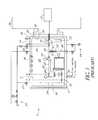
- FIG. 1is a schematic illustration of a conventional precursor source assembly and a reactor chamber assembly.
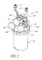
- FIG. 2is a perspective view of a conventional solid precursor source vessel.
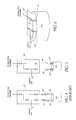
- FIG. 3is an illustration of both ideal and less than ideal source chemical concentrations in reactant gas pulses for atomic layer deposition.
- FIG. 4is a schematic illustration of a conventional precursor source vessel and gas panel.
- FIG. 5is a schematic illustration of a precursor source vessel with surface-mounted valves and a gas panel.
- FIG. 6is a schematic illustration of a precursor source vessel with surface-mounted valves and a gas panel in close thermal contact with the vessel.
- FIG. 7is a perspective view of an embodiment of a precursor source vessel, a gas interface assembly for fluidly communicating with the vessel, and a quick-connection assembly for connecting and disconnecting the vessel to the gas interface assembly.
- FIG. 8is an exploded perspective view of the vessel of FIG. 7 .
- FIG. 9is a rear perspective sectional view of the vessel of FIG. 7 .
- FIG. 10is a rear sectional view of the vessel of FIG. 7 .
- FIG. 11Ais an exploded view of another embodiment of a precursor source vessel.
- FIG. 11Bis a top perspective view of a lid for the precursor source vessel shown in FIG. 11A .
- FIG. 11Cis a bottom perspective view of the lid shown in FIG. 11B .
- FIG. 11Dis a top perspective view of an embodiment of a base for the precursor source vessel shown in FIG. 11A .
- FIG. 11Eis a top plan view of the base shown in FIG. 11D .
- FIG. 11Fis a cross-sectional view of the base shown in FIG. 11E taken along line A-A.
- FIG. 11Gis a cross-sectional view of the base shown in FIG. 11E taken along line B-B.
- FIG. 11His a cross-sectional view of another embodiment of a base for the precursor source vessel shown in FIG. 11A .
- FIG. 11Iis a top plan view of yet another embodiment of a base for the precursor source vessel shown in FIG. 11A .
- FIG. 11Jis an exploded perspective view of another embodiment of a source vessel.
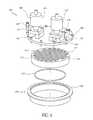
- FIG. 12is an exploded perspective view of an embodiment of a serpentine insert comprising a stack of trays.
- FIG. 13is a perspective view of an upper stacking tray of the serpentine insert of FIG. 12 .
- FIG. 14is a top view of the upper stacking tray of FIG. 13 .
- FIG. 15is a perspective view of a lower stacking tray of the serpentine insert of FIG. 12 .
- FIG. 16is a top view of the lower stacking tray of FIG. 15 .
- FIG. 17is a sectional view of a filter mounted on a lid of a precursor source vessel.
- FIG. 18is an embodiment of a filter material that can be used for the filter of FIG. 17 .
- FIG. 19is a schematic illustration of a gas delivery system for flowing carrier and reactant gases through a precursor source vessel and a vapor phase reaction chamber.
- FIGS. 20 and 21are front perspective views of the vessel and gas interface assembly of FIG. 7 , shown connected.
- FIG. 22is a top front perspective view of the precursor source vessel and gas interface assembly of FIG. 7 , with an alternative embodiment of a quick-connection assembly.
- FIG. 23is a top front perspective view of the vessel and gas interface assembly of FIG. 22 , shown connected.
- FIG. 24is a bottom front perspective view of the vessel and gas interface assembly of FIG. 22 , shown separated.
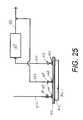
- FIG. 25is a schematic illustration of a gas delivery system for flowing carrier and reactant gases through a precursor source vessel and a reaction chamber.
- FIG. 26is a perspective view of a precursor source vessel with a vent valve.
- FIG. 27is a perspective view of the vessel of FIG. 26 connected to the gas interface assembly of FIGS. 22-24 .
- FIG. 28is a sectional view of the vessel of FIG. 26 , with the addition of a dedicated heating device for the vessel.
- the present application for letters patentdiscloses improved precursor source vessels, apparatuses and methods for loading and connecting the vessels to a reactor, and interfaces for using the vessels with vapor processing reactors.
- the disclosed embodimentsprovide excellent access to reactant vapor, reduced contamination of the reactor's gas delivery system, and improved serviceability (e.g., replacement or recharging) of the precursor source vessel.
- FIG. 1schematically illustrates a conventional precursor delivery system 6 for feeding a gas phase reactant generated from a solid or liquid precursor source vessel 10 into a gas phase reaction chamber 12 .
- Skilled artisanswill understand that the precursor delivery systems of the present invention may incorporate many of the aspects of the gas delivery system 6 of FIG. 1 . Accordingly, the conventional delivery system 6 is now described in order to better understand the invention.
- the solid or liquid source vessel 10contains a solid or liquid source precursor (not shown).
- a solid source precursoris a source chemical that is solid under standard conditions (i.e., room temperature and atmospheric pressure).
- a liquid source precursoris a source chemical that is liquid under standard conditions.
- the precursoris vaporized within the source vessel 10 , which may be maintained at or above a vaporizing temperature.
- the vaporized reactantis then fed into the reaction chamber 12 .
- the reactant source vessel 10 and the reaction chamber 12can be located in a reactant source cabinet 16 and a reaction chamber vessel 18 , respectively, which are preferably individually evacuated and/or thermally controlled. This can be achieved by providing these components with separate cooling and heating devices, insulation, and/or isolation valves and associated piping, as known in the art.
- the illustrated gas delivery system 6is particularly suited for delivering vapor phase reactants to be used in a vapor phase reaction chamber.
- the vapor phase reactantscan be used for deposition (e.g., CVD) or Atomic Layer Deposition (ALD).
- the reactant source vessel 10 and the reaction chamber 12are adapted to be in selective fluid communication with each other through a first conduit 20 so as to feed the gas phase reactant from the reactant source vessel 10 to the reaction chamber 12 (such as an ALD reaction chamber).
- the first conduit 20includes one or more isolation valves 22 a , 22 b , which may be used for separating the gas spaces of the reactant source vessel 10 and the reaction chamber 12 during evacuation and/or maintenance of either or both of the reactant source vessel 10 and the reaction chamber vessel 18 .
- Inactive or inert gasis preferably used as a carrier gas for the vaporized precursor.
- the inert gase.g., nitrogen or argon
- the reactant source vessel 10includes at least one inlet for connection to the second conduit 24 and at least one outlet for withdrawing gas from the vessel 10 .
- the outlet of the vessel 10is connected to the first conduit 20 .
- the vessel 10can be operated at a pressure in excess of the pressure of the reaction chamber 12 .
- the second conduit 24includes at least one isolation valve 26 , which can be used for fluidly isolating the interior of the vessel 10 during maintenance or replacement of the vessel.
- a control valve 27is preferably positioned in the second conduit 24 outside of the reactant source cabinet 16 .
- the precursor vaporcan be drawn to the reaction chamber 12 by applying a vacuum to the reactant source vessel 10 , without using a carrier gas. This is sometimes referred to as “vapor draw.”
- the precursor vaporcan be drawn out of the vessel 10 by an external gas flow that creates a lower pressure outside of the vessel, as in a Venturi effect.
- the precursor vaporcan be drawn by flowing a carrier gas toward the reaction chamber 12 along a path downstream of the vessel 10 . Under some conditions, this can create a pressure differential between the vessel 10 and the flow path of the carrier gas. This pressure differential causes the precursor vapor to flow toward the reaction chamber 12 .
- the gas delivery system 6includes a purifier 28 through which the vaporized reactant is conducted.
- the purifier 28may comprise one or more of a wide variety of purifying devices, such as mechanical filters, ceramic molecular sieves, and electrostatic filters capable of separating dispersed solids or particles or molecules of a minimum molecular size from the reactant gas flow. It is also known to provide an additional purifier in the vessel 10 .
- U.S. Published Patent Application No. US 2005/0000428A1discloses a vessel comprising a glass crucible enclosed within a steel container, the crucible containing the reactant source and having a lid with a filter. The lid is separate from a vessel lid that attaches to the steel container.
- the reactant source vessel 10is positioned within the reactant source cabinet 16 .
- the interior space 30 of the cabinet 16can be kept at a reduced pressure (e.g., 1 mTorr to 10 Torr, and often about 500 mTorr) to promote radiant heating of the components within the cabinet 16 and to thermally isolate such components from each other to facilitate uniform temperature fields.
- the cabinetis not evacuated and includes convection-enhancing devices (e.g., fans, cross-flows, etc.).
- the illustrated cabinet 16includes one or more heating devices 32 , such as radiation heaters.
- reflector sheets 34can be provided, which may be configured to surround the components within the cabinet 16 to reflect the radiant heat generated by the heating devices 32 to the components positioned within the cabinet 16 .
- Reflector sheets 34can be provided on the inner walls 40 of the cabinet 16 , as well as on the cabinet's ceiling 7 and floor 9 .
- a substantial length of the first conduit 20is contained within the reactant source cabinet 16 .
- the first conduit 20will inherently receive some heat to prevent condensation of reactant vapors.
- the reactant source cabinet 16can include a cooling jacket 36 formed between an outer wall 38 and an inner wall 40 of the cabinet.
- the cooling jacket 36can contain water or another coolant.
- the jacket 36allows the outer surface 38 of the cabinet 16 to be maintained at or near ambient temperatures.
- an inactive gas barrierin the first conduit 20 .
- Thisis also sometimes referred to as “inert gas valving” or a “diffusion barrier” in a portion of the first conduit 20 to prevent flow of reactant from the reactant source vessel 10 to the reaction chamber 12 by forming a gas phase barrier by flowing gas in the opposite direction to the normal reactant flow in the first conduit 20 .
- the gas barriercan be formed by feeding inactive gas into the first conduit 20 via a third conduit 50 connected to the conduit 20 at a connection point 52 .
- the third conduit 50can be connected to an inert gas source 54 that supplies the second conduit 24 .
- inactive gasis preferably fed into the first conduit 20 through the third conduit 50 .
- This gascan be withdrawn via a fourth conduit 58 , which is connected to the first conduit 20 at a second connection point 60 located upstream of the first connection point 52 (i.e., closer to the reactant source vessel 10 ).
- the fourth conduit 58can be in communication with an evacuation source 64 (such as a vacuum pump).
- a restriction 61 and valves 56 , 63 , and 70can also be provided. Further details of the gas delivery system 6 are illustrated and described in U.S. Published Patent Application No. US 2005/0000428A1.
- Some systemsutilize these additional heaters to bias the intervening components to a temperature above that of the source vessel.
- Such temperature biasinghelps to prevent precursor condensation in the intervening components during cool-down. Since the source vessel typically has a higher thermal mass than the intervening gas-conveying components, these components are at risk of cooling down to the condensation temperature faster than the source vessel. This can lead to an undesirable condition in which the source vessel is still producing precursor vapor that can flow to the cooler intervening components and deposit thereon.
- the temperature biasingcan overcome this problem.
- the need for additional heatersincreases the total size and operating cost of the apparatus.
- conventional solid source delivery systemstypically employ filters (such as the purifier 28 of FIG. 1 ) between the source vessel outlet and the substrate reaction chamber, in order to prevent solid precursor particles (e.g., powder entrained in the carrier gas flow) from entering the reaction chamber.
- filtersalso add to the total size of the apparatus and can require additional heaters to prevent condensation therein.
- filtersare typically downstream of the source vessel outlet, which involves a risk that precursor particles may deposit on gas-conveying components downstream of the vessel outlet, such as within gas conduits or within the vessel outlet valve itself. These particles can damage components such as valves, which can compromise their ability to completely seal.
- FIG. 2shows a typical precursor source vessel 31 comprising a container body 33 and a lid 35 .
- the lid 35includes inlet tubes 43 a , 43 b and outlet tubes 45 a , 45 b extending upward therefrom.
- An isolation valve 37is interposed between the inlet tubes 43 a , 43 b
- an isolation valve 39is interposed between the outlet tubes 45 a , 45 b .
- Another isolation valve 41is interposed between gas lines connecting the tubes 43 a and 45 a .
- the inlet tubes 43 a , 43 b and outlet tubes 45 a , 45 bprovide for the flow of an inert carrier gas through the container body 33 .
- the tubes 43 a , 45 atypically include fittings 47 configured to connect to other gas flow lines of the reactant gas delivery system.
- the tubes 43 a , 45 atypically include fittings 47 configured to connect to other gas flow lines of the reactant gas delivery system.
- Dead legstend to occur when the gas flow path from the precursor source vessel is longer and more complex.
- Conventional inlet and outlet isolation valves for the source vesselcan produce dead legs.
- dead legsincrease the risk of unwanted precursor deposition on the gas-conveying components of the delivery system.
- Such unwanted precursor depositioncan occur due to cold spots associated with the dead volumes, wherein the precursor solidifies at temperatures below the sublimation/melting temperature.
- Such unwanted precursor depositioncan also occur due to hot spots associated with the dead volumes, wherein the precursor decomposes at high temperatures. For this reason, it is generally desirable to reduce and minimize stagnation of the reactant gas flow. It is also generally desirable to reduce the surface area to be temperature-controlled, in order to lessen the chance of producing hot or cold spots.
- the minimum pulse timeis the pulse time necessary for an injected reactant to saturate the surface of a substrate being processed.
- the minimum purge timeis the time necessary to purge excess reactant from the substrate reaction chamber and gas delivery system between reactant pulses.
- Substrate throughput(the rate at which substrates can be processed) is increased when the minimum pulse time and minimum purge time are decreased. Accordingly, it is desirable to reduce the amount and volume of dead legs in order to increase throughput.
- the pulse shaperefers to the shape of a curve of the reactant's chemical concentration in the reactant/carrier mixture, for a reactant gas pulse.
- FIG. 3shows an example of an ideal reactant concentration curve 80 , as well as a curve 82 that is less than ideal. Both curves include reactant gas pulses 84 separated by time periods 86 of substantially zero reactant concentration.
- the ideal curve 80resembles a rectilinear wave, such as a square wave.
- a substantially rectilinear waveis preferred because it is highly desirable for each reactant gas pulse to deliver the reactant species to all of the available reaction sites on the substrate surface (saturation) in the least amount of time, in order to optimize substrate throughput.
- a rectilinear pulse shapeas in the curve 80 , optimizes throughput because the duration of each pulse has a high concentration of the reactant, which in turn reduces the pulse duration necessary to deliver sufficient reactant species to the substrate surface. Also, the reduced dispersion of a rectilinear pulse shape reduces the amount of “pulse overlap” between successive pulses of different precursors, which reduces the potential for unwanted CVD growth modes.
- the pulse concentration of each pulse 84 of the non-ideal curve 82takes longer to reach its maximum level, which increases the pulse duration necessary to fully saturate the substrate surface.
- the frequency of the curve 80is less than that of the curve 82 .
- Precursor source vesselsare typically supplied with a head pressure of gas in the vessel.
- a source vessel filled with precursor powderis often shipped with helium or other inert gas at a pressure slightly higher (e.g., 5 psi) than ambient pressure.
- Heliumis typically used to enable an “out-bound” helium leak test using a helium leak detector to ensure vessel integrity just prior to shipment. This helium is often left or replaced with N 2 or other inert gas so that if a small leak is present, the gas leaks outward from the vessel, preventing atmospheric contamination of the precursor within the vessel.
- the vessel's internal gasis vented out through the vessel's outlet isolation valve, through the reactant gas delivery system, and ultimately through the reactor's exhaust/scrubber.
- the vessel's internal gasis vented out through the substrate reaction chamber.
- Other systemsemploy a gas line in parallel with the reaction chamber (i.e., extending from a point just upstream of the reaction chamber to a point just downstream of the reaction chamber), such that the vessel's internal gas can be directed to the exhaust/scrubber without flowing through the reaction chamber. In either case, current vessel designs involve a risk of particle generation when the vessel is relieved of the head pressure.
- precursor powderbecoming entrained within the vent flow (i.e., the venting out of the internal pressurized gas of the vessel), which can contaminate and possibly damage downstream components of the gas delivery system, including the vessel outlet itself.
- precursor materiale.g., powder
- precursor materialcan become entrained within the carrier gas flowing through the precursor source vessel, which involves a risk of unwanted deposition of the precursor within the gas delivery system.
- precursor delivery systemssubstantially overcome these problems by employing an improved precursor source vessel and apparatus for quickly connecting and disconnecting the vessel from the rest of the delivery system.
- FIGS. 4-6illustrate three different gas panel arrangements.
- a gas paneltypically includes one or more valves that are downstream of a precursor source vessel, and can also include one or more valves upstream of the vessel.
- FIG. 4illustrates a conventional arrangement in which a source chemical is contained within a source vessel 10 .
- a gas panel 90includes a plurality of valves operable to deliver carrier gas from a carrier gas source (not shown) through the vessel 10 and into a reaction chamber (not shown).
- An inlet valve 91is connected upstream of the vessel 10 by tubing 93
- an outlet valve 92is connected downstream of the vessel 10 by tubing 94 .
- the inlet valve 91 , the outlet valve 92 , and the valves and tubing of the gas panel 90are typically not in close thermal contact with the vessel 10 .
- FIG. 5illustrates an arrangement that is somewhat improved relative to that of FIG. 4 .
- a precursor source vessel 100has a surface-mounted inlet valve 108 and a surface-mounted outlet valve 110 .
- the valves 108 and 110are separated from a conventional gas panel 90 by tubing 95 and 96 .
- the valves 108 and 110are in close thermal contact with the vessel 100 , but the valves and tubing of the gas panel 90 are not.
- FIG. 6illustrates an arrangement that is improved relative to that of FIG. 5 .
- the source vessel 100has a generally flat upper surface with a surface-mounted inlet valve 108 and a surface-mounted outlet valve 110 .
- a gas panel 97is arranged such that the valves and tubing of the gas panel are positioned along a plane that is generally parallel to the generally flat surface of the vessel 100 .
- the distance between the plane of the gas panel valves and tubing and the generally flat surface of the vessel 100is preferably no more than about 10.0 cm, more preferably no more than about 7.5 cm, and even more preferably no more than about 5.3 cm.
- FIG. 7shows an embodiment of an improved solid or liquid precursor source vessel 100 and a quick-connection assembly 102 .
- the source vessel 100includes a container body 104 and a lid 106 .
- the lid 106includes surface-mounted isolation valves 108 and 110 , described in more detail below.
- FIGS. 8-10show the source vessel 100 of FIG. 7 in greater detail.
- FIG. 8is an exploded view
- FIGS. 9 and 10are rear cross-sectional views, of the source vessel 100 .
- the illustrated vessel 100includes the container body 104 , a serpentine pathway insert 112 within the body 104 , and the lid component 106 .
- the illustrated assemblyis fastened together by fastening elements 124 , such as screws or nut and bolt combinations.
- the fastening elements 124are adapted to extend into aligned holes within a flange 126 of the body 104 . Skilled artisans will appreciate that the assembly can be fastened together by a variety of alternative methods.
- the serpentine pathway insert 112preferably defines a tortuous or serpentine pathway 111 through which a carrier gas must travel as it flows through the vessel 100 .
- the serpentine pathway 112preferably contains the precursor source, such as a powder or liquid.
- the serpentine pathway 111is significantly longer than the carrier gas flow pathway within conventional precursor source vessels.
- the valves 108 and 110 (described below) and the valve 210 (described below with reference to FIGS. 26-28 )are subjected to a less severe environment, thereby increasing their reliability.
- a spring 114is preferably provided to bias the serpentine insert 112 against the lid 106 , to prevent the escape of reactant gas through the interface between the insert 112 and the lid 106 .
- the spring 114tends to reduce the risk of the gas bypassing some or all of the serpentine path.
- Suitable springs 114include flat wire compression springs, such as the Spirawave® wave springs sold by Smalley Steel Ring Company of Lake Zurich, Ill.
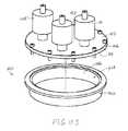
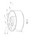
- FIG. 11Ashows another embodiment of an improved solid or liquid precursor source vessel 400 that includes a container base 402 , a seal 404 , and a lid 406 .
- the lid 406includes a plurality of integrated gas valves, or surface-mounted valves, described in more detail below.
- FIGS. 11B-11Cillustrate an exemplary embodiment of the lid 406 .
- FIGS. 11D-11Gshow an embodiment of the base 402 of the source vessel 400 .
- FIGS. 11H-11Ishow other embodiments of the base 402 of the source vessel 400 .
- the base 402is formed of a solid member that includes a recessed region 408 that is machined directly into the solid base 402 .
- a seal 404is disposed therebetween prior to the lid 406 being secured to the base 402 to ensure the contents within the source vessel 400 are secured therewithin.
- the base 402 and the lid 406are formed of the same material such that both members have substantially the same thermal conductivity and the same coefficient of thermal expansion therebetween.
- the base 402is formed of a material different than the material used to form the lid 406 .
- the base 402 and the lid 406are formed of stainless steel.
- the base 402 and/or lid 406may be formed of high nickel alloys, aluminum, or titanium. It should be understood by one of ordinary skill in the art that the base 402 and the lid 406 can be formed of any other material sufficient to allow sufficient thermal heat transfer to vaporize the precursor disposed within the source vessel 400 while being inert, or not reacting with the precursor or contents within the source vessel 400 .
- a seal 404is disposed between the base 402 and the lid 406 of the source vessel 400 , as shown in FIG. 11A .
- the seal 404is an o-ring that is disposed within a groove 410 formed in the base 402 .
- the seal 404can be formed as a metal gasket or a v-seal that is configured to be disposed between the base 402 and the lid 406 .
- the seal 404can be formed of any shape, size, or configuration sufficient to provide a seal when the lid 406 is attached to the base 402 and to ensure that the contents within the source vessel 400 are secured therewithin.
- the seal 404is formed of an elastomer, but it should be understood by one of ordinary skill in the art that the seal 404 may be formed of any other material sufficient to provide a seal, such as, but not limited to, polymer or metal.
- the lid 406is formed as a single member having an upper surface 412 , a lower surface 414 , and a side surface 413 extending between the upper and lower surfaces 412 , 414 .
- the upper and lower surfaces 412 , 414are substantially planar surfaces. It should be understood by one skilled in the art that the planar upper and lower surfaces 412 , 414 may further include indentations, grooves, apertures, or inset portions formed therein.
- the upper and lower surfaces 412 , 414are substantially parallel to each other, thereby providing the lid 406 with a consistent thickness T 1 across the entire lid 406 .
- the upper surface 412may include high-tolerance areas 416 that are machined so as to provide a substantially smooth area relative to the rest of the upper surface 412 .
- These high-tolerance areas 416allow the valve assemblies 418 to be mounted flush with the upper surface 412 of the lid 406 to ensure as much direct thermal contact between the valve assemblies 418 and the lid 406 . With more surface area contact between these components, the heat transfer between these components can be maximized, thereby reducing the need for separate heaters or heating jackets to provide heat to the valve assemblies 418 which prevents condensation of vaporized precursor therewithin.
- the lid 406includes an inlet port 420 , an outlet port 422 , and a burp port 424 .
- the inlet port 420is configured to allow a carrier gas, or an inert gas, to be introduced into the source vessel 400 therethrough.
- the outlet port 422is configured to allow gases to exit the source vessel 400 therethrough.
- the burp port 424may comprise any port, such as a conventional inlet/outlet port, that may be configured to relieve head pressure within the source vessel 400 after either the initial fill and installation of the source vessel 400 or after subsequent re-fills and installations of the source vessel 400 . The release of head pressure through the burp port 424 is done prior to the source vessel 400 providing vaporized precursor material to the reaction chamber 162 ( FIG.
- an interface component 426is operatively attached to the upper surface 412 of the lid 406 at each of the ports 420 , 422 , 424 .
- Each interface component 426is configured to be connected to a valve assembly 418 . It should be understood by one of ordinary skill in the art that each valve assembly 418 and an interface component 426 may be operatively connected to the upper surface 412 of the lid 406 in any manner.
- one of the valve assemblies 418includes a vent valve, or burp valve 428 that is operatively connected to the upper surface 412 of the lid 406 .
- the burp valve 428can be a pneumatic valve or any other valve that regulates the flow of gases into and out of the source vessel 400 .
- the burp valve 428remains closed except when opened for release of gases to relieve the head pressure within the source vessel 400 prior to use of the source vessel 400 in a semiconductor processing system.
- an inert gasis introduced into the source vessel 400 so as to create a head pressure within the source vessel 400 .
- This head pressureis used to allow a leak check to be performed once the source vessel 400 is filled (or refilled), as explained above.
- the gases within the source vessel 400 that create the head pressureneed to be removed and replaced with the inert carrier gas that will be used to carry the vaporized precursor during processing.
- the head pressurewas relieved from source vessels commonly known in the art by exhausting the gases creating the initial head pressure through an outlet port which is the same outlet port through which vaporized precursor material exits during processing of a substrate.
- a filter adjacent to the outlet portwould often become clogged by precursor particles that accompanied the gases during an initial “burp” process or release.
- the precursor particleswere stopped by the outlet filter, some particles are able to bypass the filter—or particles caught by the filter would subsequently become dislodged—and enter into the tubing that leads to the reaction chamber.
- These errant precursor particlescan cause non-uniform deposition within the reaction chamber or clog the gas lines between the source vessel and the reaction chamber.
- the errant particlesmay also cause particle entrainment on the semiconductor substrate being processed, thereby resulting in a reduction of the number of devices, chips, or circuits that the substrate can produce.
- the burp port 424 and corresponding burp valve 428 of the present inventionallow the head pressure to be relieved during a “burp” process in which the gases and particles exiting the burp port 424 are first filtered by a burp filter 430 before being diverted through a burp gas line 432 that is connected directly to the exhaust line 466 ( FIG. 25 ), thereby bypassing the reaction chamber 162 so as to prevent any unwanted particles from interfering with processing within the reaction chamber 162 .
- a filtration apparatus 434is operatively connected to the bottom surface 414 of the lid 406 .
- a filtration apparatus 434is configured to filter the carrier gas being introduced through the lid 406 into the source vessel 400 as well as the gases exiting the source vessel 400 through the burp port 424 and the outlet port 422 .
- a filtration apparatus 434is attached to the underside of the lid 406 adjacent to the inlet port 420 , the outlet port 422 , and the burp port 424 .
- the filtration apparatuses 434are attached directly to the lid 406 to allow a sufficient amount of heat transfer from the lid 406 to prevent condensation of precursor material within each filtration apparatus 434 .
- Each filtration apparatus 434preferably has a low-profile, because a low-profile filtration apparatus provides good thermal uniformity across the filter pack media ( FIG. 17 ).
- the base 402includes a body 436 and a flange 438 that is integrally connected to the body 436 and extends therefrom.
- the body 436 and the flange 438are formed from a single piece of material.
- a groove 410is formed into the body 436 , wherein the groove 410 is configured to receive the seal 404 .
- the flange 438is configured to extend radially outward from the upper portion of the body 436 .
- the base 402is defined by an upper, contact surface 440 , a bottom surface 442 , a side surface 444 , and an inner surface 446 that defines and forms the recessed region 408 .
- the contact surface 440is a substantially planar surface that forms the entire upper surface of the base 402 .
- the contact surface 440is configured to directly contact the lower surface 414 of the lid 406 .
- the base 402is a solid piece of material or metal into which the recessed region 408 is machined, or removed, as illustrated in FIGS. 11D-11G .
- the base 402is formed as a one-piece casting in which the recessed region 408 is formed into the base 402 during the casting or forging process.
- the recessed region 408is configured to receive a solid or liquid precursor therewithin.
- the recessed region 408is formed as an elongated, tortuous pathway extending from the contact surface 440 of the base 402 .
- the inner surface 446extends from the contact surface 440 into the thickness of the body 436 .
- the depth that the recessed region 408 is formed into the body 436may vary. It should be understood by one of ordinary skill in the art that the shape, depth, and width of the recessed region 408 may vary so long as the recessed region 408 allows for an extended flow path between the inlet and outlet ports 420 , 422 in order to increase the residence time of gases with the precursor material disposed within the recessed region 408 .
- the recessed region 408includes an inlet recessed pad 448 , an outlet recessed pad 450 , a burp recessed pad 452 , and a channel 454 that fluidly connects the recessed pads 448 , 450 , 452 .
- the recessed pads 448 , 450 , 452are generally triangular-shaped recessed regions extending downwardly from the contact surface 440 of the base 402 .
- the shape of the recessed pads 448 , 450 , 452are substantially the same shape and size of the portion of the corresponding filtration apparatus 434 that extends from the lower surface 414 of the lid 406 into the base 402 such that a portion of each filtration apparatus 434 is received within a corresponding recessed pad 448 , 450 , 452 .
- the recessed pads 448 , 450 , 452extend downwardly from the contact surface 440 to a predefined depth. In an embodiment, the depth of all of the recessed pads 448 , 450 , 452 is the same. In another embodiment, the depth of at least one of the recessed pads 448 , 450 , 452 is different than the depth of the others.
- each of the recessed pads 448 , 450 , 452When the base 402 is filled with precursor, the volume within each of the recessed pads 448 , 450 , 452 is not filled with precursor.
- a carrier gasis introduced into the base 402 through the filtration apparatus 434 adjacent to the inlet port 420 of the lid 406 , the carrier gas contacts and is distributed within the inlet recessed pad 448 before traveling throughout the remainder of the recessed region 408 . Because there is preferably no precursor located within any of the recessed pads 448 , 450 , 452 , the introduction of a carrier gas into the inlet recessed pad 448 prevents the carrier gas from directly contacting the precursor and potentially stifling up the precursor or causing particles of the precursor to be intermixed with the carrier gas.
- Each of the recessed pads 448 , 450 , 452 of the recessed region 408is fluidly connected by way of the channel 454 formed into the body 436 .
- the channel 454 of the recessed region 408extends from the contact surface 440 , wherein the channel 454 is a continuous pathway along which gases can travel between the inlet recessed pad 448 and the outlet recessed pad 450 .
- the recessed region 408does not include recessed pads such that the channel 454 extends the entire distance between the filtration apparatus 434 adjacent to the inlet port 420 and the filtration apparatus 434 adjacent to the outlet and burp ports 422 , 424 .
- the channel 454is formed into the body 436 such that the channel 454 has a depth that is greater than the depth of the recessed pads 448 , 450 , 452 .
- the depth of the channel 454is constant along the entire length of the channel 454 between the inlet recessed pad 448 and the outlet recessed pad 450 . In another embodiment, the depth of the channel 454 varies along the length of the channel 454 between the inlet recessed pad 448 and the outlet recessed pad 450 .
- the precursor materialis preferably disposed only within the channel 454 of the recessed region 408 formed in the body 436 .
- the channel 454should be filled to a depth that is below the bottom surface of the recessed pads 448 , 450 , 452 to prevent any of the precursor material from being disposed within the recessed pads 448 , 450 , 452 .
- the bottom surface of the outlet recessed pad 450is located above the upper surface of the precursor material such that any precursor material particles remain within the channel 454 .
- the channel 454extends between the inlet recessed pad 448 and the outlet recessed pad 450 and has a serpentine shape.
- the channel 454forms a tortuous pathway between the inlet and outlet ports 420 , 422 along which a carrier gas can travel.
- the channel 454 between the inlet and outlet recessed pads 448 , 450is non-linear between the inlet and outlet ports 420 , 422 .
- the channel 454includes a plurality of linear sections 456 . Further, at least two adjacent linear sections 456 are substantially parallel to each other.
- the channel 454has a width.
- the channel 454has a constant width along the entire length thereof. In another embodiment, the width of the channel 454 varies along the length thereof.
- the serpentine shape of the channel 454maximizes the amount of time and distance that the carrier gas introduced into the source vessel 400 is in contact with precursor material disposed within the recessed region 408 .
- the channel 454extends between, and is in fluid communication with, the inlet recessed pad 448 and the outlet recessed pad 450 , as illustrated in FIG. 11H .
- the channel 454includes a plurality of arced sections 458 .
- the channel 454includes at least two arced sections 458 that are substantially concentric with respect to each other.
- the channel 454includes a plurality of arced sections 458 but no linear sections 456 .
- the channel 454is a completely random, tortuous pathway extending between the inlet recessed pad 448 and the outlet recessed pad 450 or between the inlet and outlet ports 420 , 422 .
- FIG. 11Hillustrates an embodiment of a base 402 that further includes a heating assembly 460 disposed within the base 402 .
- the heating assembly 460is integrated into the walls of the base 402 between the side and bottom surfaces 444 , 442 and the inner surface 446 .
- the heating assembly 460is configured to provide direct heat to the base 402 so as to vaporize the precursor material 464 disposed therewithin.
- the heating assembly 460may be a wire heater integrally formed within the base, or any other type of heating mechanism sufficient to provide direct heat to the base 402 while being integrated therewithin.
- the heating assembly 460may also be a resistive element embedded in the base 402 .
- the heating assembly 460may be a thin foil heating element embedded within the base 402 . It should be understood by one of ordinary skill in the art that the heating assembly 460 may include any heating means that provides direct heating to the body 436 of the base 402 so as to provide a sufficient amount of heat to vaporize the precursor material 464 .
- a recessed region 408is formed into the base 402 to provide a generally hollow volume within the base 402 to receive a precursor material, as shown in FIG. 11J .
- the embodiment illustrated in FIG. 11Jdoes not include a channel or tortuous pathway similar to the embodiments above, the recessed region 408 provides for an extended, non-linear pathway within the base 402 between the inlet and outlet ports 420 , 422 .
- the lid 406When the source vessel 400 is assembled, the lid 406 is removably attached to the base 402 with the seal 404 disposed therebetween. When the lid 406 is attached to the base 402 , an interior volume 468 is defined between the inner surface 446 that forms the recessed region 408 in the base 402 and the lower surface 414 of the lid 406 .
- the lid 406includes a plurality of apertures 462 formed through the entire thickness T 1 thereof, as shown in FIG. 11B .
- the apertures 462 formed through the lid 406are located adjacent to the outer edge of the lid 406 .
- the base 402also includes a plurality of apertures 462 formed through the entire thickness of the flange 438 , as shown in FIG. 11D .
- the lid 406is aligned with the base 402 such that each of the filtration apparatuses 434 attached to the lid 406 are received within a corresponding recessed pad 448 , 450 , 452 of the base 402 .
- the seal 404is disposed within the groove 410 formed in the base 402 .
- the apertures 462 formed in the lid 406likewise are aligned with the apertures 462 formed in the base 402 .
- a connecting member(not shown) is inserted through each pair of corresponding apertures 462 in the base 402 and lid 406 such that the lid 406 is removably sealed to the base 402 .
- any type of connecting membercan be used to removably attach the lid 406 to the base 402 , including, but not limited to, screws, bolts, or clamps.
- the lower surface 414 of the lid 406is in abutting contact with the contact surface 440 of the base 402 .
- the contact between the lid 406 and the contact surface 440 of the base 402provides for direct heat transfer between the lid 406 and the portions of the body 436 immediately adjacent to the recessed region 408 so as to transfer heat through the base 402 to the precursor material disposed within the interior volume 468 .
- the lower surface 414 of the lid 406 and the contact surface 440 of the base 402are both substantially planar such that when these surfaces 414 , 440 are in contact with each other, the abutting relationship between the lid 406 and the base 402 provides a seal between adjacent portions of the channel 454 ( FIGS. 11E and 11I ) so that carrier gas and vaporized precursor material does not bypass the portions of the channel 454 by passing between the lid 406 and the base 402 .
- a carrier gasin introduced into the source vessel 400 through the inlet port 420 in the lid 406 .
- a precursor material 464is disposed within the source vessel 400 , and the source vessel 400 is heated, thereby vaporizing the precursor material.
- the carrier gasthen passes through the filtration apparatus 434 located adjacent to the inlet port 420 and then into the interior volume 468 of the base 402 defined by the inner surface 446 forming the recessed region 408 and the lower surface 414 of the lid 406 .
- the carrier gasenters the inlet recessed pad 448 and then disperses through the channel 454 .
- the carrier gasAs the carrier gas travels through the interior volume 468 , the carrier gas mixes with the vaporized precursor material 464 ( FIG. 11H ) to form a gas mixture that is saturated with the vaporized precursor material.
- the longer the residence time in which the carrier gas remains within the interior volume 468the more saturated with vaporized precursor material the carrier gas becomes. It should be understood by one of ordinary skill in the art that there is a limit to the saturation level of the carrier gas by the vaporized precursor material, and the length of the pathway within the interior volume 468 between the inlet and outlet ports 420 , 422 is optimized to maximize the amount of saturation of the carrier gas.
- This gas mixtureeventually exits the interior volume 468 by passing through the filtration apparatus 434 operatively connected to the lid 406 and located adjacent to the outlet port 422 . After passing through the filtration apparatus 434 , the gas mixture exits the source vessel 400 through the outlet port 422 and into the outlet gas line 470 ( FIG. 25 ) that is in fluid communication with a reaction chamber 162 .
- burp processIn a burp process, the gas or gases within the interior volume 468 of the source vessel 400 creating a head pressure therewithin that are added after the initial fill or refill of the source vessel 400 are removed.
- the burp valve 428is opened to allow the gases within the source vessel 400 to exit the interior volume 468 through the burp port 424 .
- the head pressure gasespass through the burp filter 430 operatively connected to the lid 406 adjacent to the burp port 424 .
- the head pressure gasexits the source vessel 400 through the burp port 424 and into a burp gas line 432 that bypasses the reaction chamber 162 and is fluidly and operatively connected to an exhaust line 466 through which effluent from the reaction chamber 162 flows.
- a carrier gasis introduced through the filtration apparatus 434 attached to the lid 406 located adjacent to the inlet port 420 and then into the interior volume 468 of the base 402 to fill the recessed region 408 with the carrier gas to a pre-determined operating pressure.
- the serpentine insert 112comprises a plurality of stacked trays that collectively define a serpentine gas flow path.
- FIG. 12shows a plurality of stacked trays 230 , 240 that are configured to be removably inserted into a container body 104 ( FIGS. 7-10 ) and that collectively define a spiral gas flow path that comprises at least a portion of the tortuous path of the vessel 100 .
- the heights of the trays 230 , 240are enhanced for ease of illustration. It should be understood that the trays can be made vertically thinner so that the vessel 100 has a diameter significantly greater than its overall height.
- four traysare stacked: three upper trays 230 and one lower tray 240 .
- the number of trayscan vary based on parameters such as the sublimation rate, carrier flow, etc.
- each upper tray 230includes a solid divider 231 , preventing gas flow therethrough and extending the full height of the tray 230 , and a partial divider 232 that allows gas flow therethrough.
- the partial dividerincludes a screen 233 configured to retain large precursor particulates while allowing free gas flow therethrough.
- the screen 233extends across the top portion of the partial divider 232 , while a solid panel completes the height of the partial divider 232 .
- An annular rim 234also extends the height of the upper tray 230 .
- the solid divider 231 and the partial divider 232together define a main compartment 235 for holding solid source material (not shown) and an outer channel compartment 236 that is open at the lower surface of the tray 230 .
- the illustrated upper tray 230has a central core 237 that includes a central channel 238 to accommodate a gas inlet pipe that delivers carrier gas to the bottom tray 240 .
- the illustrated upper tray 230also has a plurality of pegs 239 on an upper surface thereof and a corresponding plurality of holes (not shown) on a bottom surface thereof for receiving the pegs of another tray therebelow.
- the holes on the lower surface of the central core 237are desirably rotationally offset relative to the pegs 239 on the upper surface, serving to properly align the plurality of trays upon one another to define the winding flow path.
- the corners in the main compartment to which the flow is exposedare rounded to minimize flow stagnation from sharply angled corners.
- the lowest tray 240comprises a solid divider 241 , preventing gas flow therethrough and extending the full height of the tray 240 , and a partial divider 242 that allows gas flow thereover.
- the partial divider 242simply provides an opening to the central channel 238 in the middle of the overlying upper tray 230 , as will be better understood in view of the description of FIG. 12 .
- An annular rim 244also extends the height of the lower tray 240 .
- the rim 244 , the solid divider 241 and the partial divider 242together define a main compartment 245 for holding solid source material (not shown) and an outer channel compartment 246 .
- the solid source materialonly fills the main compartment 245 up to and even with channel compartment 246 . In alternate embodiments, the solid source material fills the between one third and two thirds of the height of the main compartment.
- the illustrated lower tray 240also has a central core 247 into which the channel compartment 246 protrudes, a plurality of pegs 249 on an upper surface thereof and a corresponding plurality of holes (not shown) on a bottom surface thereof for receiving pegs that protrude upwardly from a floor of the container body 104 ( FIGS. 7-10 ).
- the stack of trays 230 , 240is assembled as shown in the exploded view of FIG. 12 .
- the main compartments 235 , 245 for each of the upper trays 230 and the lower tray 240are loaded with a precursor source chemical, preferably in the form of powder.
- the lower tray 240 and plurality of upper trays 230are stacked upon one another and loaded into the external container body 104 .
- the trays 230 , 240are aligned by the pegs 239 , 249 and corresponding holes such that gas flows into each tray, preferably at least flowing a lap of within 200°-355° around the main compartment and then up into the channel compartment 236 of the overlying upper tray 230 .
- the container lid 106FIGS.
- FIG. 12shows the central pipe 215 but not the lid 106 .
- the central pipe 215is configured to deliver carrier gas conveyed into an inlet of the vessel 100 .
- a spring or other biasing device(not shown) is often placed below 240 to bias all the trays together, preventing leaks from the central core to a different level.
- inert gasis preferably delivered to the stack of trays 230 , 240 , and experiences a long and winding flow route horizontally, preferably through an arc of about 200°-350° of the main compartment in each tray 230 , 240 before vertically exiting that tray.
- inert carrier gasis provided through a central inlet 215 that extends down through the aligned central channels 238 of the upper trays 230 to open into the channel compartment 246 of the lower tray 240 .
- the inert gaswinds through the precursor source chemical in the main compartment 245 until encountering an opening in the lower surface of the overlying upper tray 230 .
- This openingallows the carrier gas, and the vaporized precursor it carries with it, to pass into the channel compartment 236 of the overlying upper tray 230 , from which the gas passes through the screen 233 ( FIG. 13 ) and into the main compartment 235 .
- the gaswinds through solid precursor in that main compartment 235 , preferably through an arc of about 200°-350° before encountering an opening in the lower surface of the overlying upper tray 230 , etc.
- the gasis allowed to exit the vessel 100 , preferably through a surface-mounted outlet valve 110 (described below) at the lid vessel 106 .
- the flow pathcan be reversed if desired. In other words, the inert carrier gas can begin in a top tray and flow downward through the stack of trays.
- the vessel lid 106includes an inlet valve 108 and an outlet valve 110 .
- the inlet valve 108has an inlet end that receives carrier gas via a conduit 121 .
- the conduit 121has a fitting 122 adapted for connection to a fitting 131 ( FIG. 7 ) of a gas line 133 of a gas interface assembly 180 (described below).
- the inlet valve 108also has an outlet end that is preferably in fluid communication with a first portion 117 (such as an end portion) of the serpentine path 111 of the insert 112 .
- the outlet valve 110has an inlet end that is preferably in fluid communication with a second portion 119 (such as an end portion) of the serpentine path 111 , and an outlet end in fluid communication with a suitable gas outlet of the lid 106 , such as an orifice 128 .
- carrier gasflows into the conduit 121 and through the inlet valve 108 , serpentine path 111 , and outlet valve 110 before exiting from the orifice 128 .
- results that may be achieved by this embodimentinclude mounting the isolation valves onto the surface of the lid 106 , and causing the carrier gas to flow along a tortuous or serpentine path while it is exposed to the precursor source.
- Skilled artisanswill appreciate that the vessel 100 can be configured differently.
- conventional solid or liquid precursor source vesselsinclude discrete tubes that extend from the vessel body or lid, with the valves being attached inline with such tubes.
- the conventional vessel 31 of FIG. 2includes discrete tubes 43 b and 45 b extending upward from the lid 35 , with the valves 37 and 39 being attached to such tubes.
- the valves 37 and 39 of the vessel 37are not directly attached to or in contact with the lid 35 .
- the reactant gas from the vessel 31flows out of the outlet tube 45 b and then into the outlet valve 39 , which may involve a flow path with stagnant or dead gas volumes.
- the isolation valves 37 , 39 , and 41 of the conventional vessel 31are significantly thermally isolated from the vessel lid 35 and body 33 .
- valvesare very difficult to effectively heat with three-dimensional geometry, regardless of the presence or absence of dead volumes or “dead legs.”
- the valveshave a smaller thermal mass than the lid 35 and body 33 and therefore tend to heat up and cool down faster. That is why, in conventional systems, additional heaters (such as line heaters, cartridge heaters, directed heat lamps, etc.) are often used specifically to provide heat to the valves and associated tubing during system cool-down, to prevent such components from cooling down faster than the vessel 31 (which can create an unwanted condition in which reactant vapors flow into such components and deposit thereon).
- Another problem with the conventional valves and tubingis that they can heat up faster than the vessel 31 . For some precursors, this can create a condition in which the valves and tubing become warmer than the decomposition temperature of the precursor, causing the precursor to decompose and deposit thereon.
- the isolation valves 108 and 110( FIGS. 7-10 ) of the source vessel 100 are preferably mounted directly to the surface of the lid 106 of the vessel 100 .
- Such surface mount technologymay be referred to as an integrated gas system.
- the surface-mounted valves 108 and 110can reduce the volume of dead legs (stagnant reactant gas flow) in the gas delivery system by eliminating tubing between the valves and the vessel 100 , which simplifies and shortens the travel path of the reactant gas.
- the valves and tubingare much more amenable to heating due to the compressed geometry and improved thermal contact, which lessens temperature gradients.
- valve porting blocks 118 and 120respectively, which preferably include valve seats and adjustable flow restrictors (e.g., diaphragms) for selectively controlling gas flow through the valve seats.
- valves 108 and 110isolate the vessel 100 by restricting all gas flow through the valve seats.
- the porting blocks 118 , 120can be formed integrally with the vessel lid 106 or can be separately formed and mounted thereon. In either case, the porting blocks 118 , 120 preferably have a relatively high degree of thermal contact with the vessel lid 106 . This causes the temperatures of the valves 108 and 110 to remain close to that of the lid 106 and container body 104 during temperature changes of the vessel 100 .
- This surface-mounted valve configurationcan reduce the total number of heaters required to prevent condensation of vaporized precursor gas.
- vaporized precursorcan freely flow to the valves 108 and 110 . Since the valves 108 , 110 closely track the temperature of the vessel 100 during temperature ramping, the valves are also likely to be above the vaporization temperature, thus reducing the need for additional heaters to prevent condensation of the precursor in the valves.
- the shortened gas flow pathsare also better suited for controlled heating.
- the surface-mounted valves 108 and 110also have a much smaller packaging space requirement.
- the valving of the porting blocks 118 , 120can be integrally formed within the lid 406 of the source vessel 400 , thereby allowing the inlet and outlet valves 108 , 110 as well as a burp valve 428 to be attached directly to the lid 406 such that the inlet, burp, and outlet valves 108 , 428 , 110 are mounted flush with the upper surface 412 of the lid 406 , as illustrated in FIG. 11J . Mounting the valves directly and flush with the upper surface 412 of the lid 406 increases the heat transfer therebetween as well as further reduce the distance the inert gas and vaporized precursor mixture must travel from the interior volume 468 of the base 402 to the reaction chamber 162 ( FIG. 25 ).
- Each of the valves 108 and 110preferably comprises a valve porting block including gas flow passages that can be restricted or opened by the valve.
- the porting block 118 of valve 108preferably includes an internal gas flow passage extending from the conduit 121 through one side 123 of the porting block 118 to a region 113 .
- the region 113preferably includes an internal apparatus (not shown) for restricting the flow of the gas, such as a valve seat and a movable restrictor or diaphragm.
- the movable internal restrictor or diaphragmcan be moved by turning a knob (e.g., the larger cylindrical upper portion 181 of the valve 108 ) either manually or in an automated fashion.
- Another internal gas flow passagepreferably extends from the region 113 through an opposite side 125 of the block 118 to an inlet passage that extends through the lid 106 into the vessel 100 .
- the inlet passagecan extend into the tortuous path 111 defined by the serpentine insert 112 .
- the valve 110 and vent valve 210(described below with reference to FIGS. 26-28 ) can be configured similarly to valve 108 .
- the valves 108 and 110are pneumatic valves. It is particularly preferred to form the valve porting blocks 118 and 120 integrally with the vessel lid 106 . This eliminates the need for separate seals therebetween.
- valves 108 , 110 , and 210are formed without porting blocks, such as porting blocks 118 , 120 , and are preferably formed integrally with a portion of the vessel 100 , such as the vessel lid 106 .
- the precursor source vesselincludes a filtration apparatus for filtering the gas flow through the vessel, to prevent particulate matter (e.g., the source chemical's powder) from escaping the vessel.
- the filtration apparatuscan be provided in a lid of the vessel, preferably underneath a surface-mounted valve 108 , 110 , and/or 210 ( FIGS. 26-28 ).
- the filtration apparatuscomprises a separate filter for each inlet and outlet of the vessel.
- FIG. 17is a sectional view of one embodiment of a filtration apparatus 130 , which can be installed in the body or lid (e.g., lid 106 of FIG. 8 ) of a reactant source vessel.
- the illustrated apparatus 130is a filter formed of a flange 132 , a filter media 134 , and a fastener element 136 .
- the filter 130is sized and shaped to fit closely into a recess 138 of the vessel's lid (e.g., lid 106 of FIG. 8 ).
- the perimeter of the flange 132can be circular, rectangular, or other shapes, and the shape preferably conforms tightly to the perimeter of the recess 138 .
- the filter material 134is configured to restrict the passage of gas-entrained particles greater than a certain size through an opening defined by an annular inner wall 140 of the flange 132 .
- the material 134preferably blocks the entire opening defined by the wall 140 .
- the material 134can comprise any of a variety of different materials, and in one embodiment is a high flow sintered nickel fiber media.
- the filter mediais manufactured from other metals (e.g., stainless steel), ceramics (e.g., alumina), quartz, or other materials typically incorporated in gas or liquid filters.
- the material 134is preferably welded or adhered to the annular wall 140 .
- the filter 130comprises a surface-mount sandwich filter, such as those sold by TEM Products of Santa Clara, Calif.
- the fastener element 136comprises a spring snap ring that biases the flange 132 against a wall 146 of the lid 106 .
- the ring 136preferably fits closely within an annular recess 142 in the perimeter of the recess 138 .
- the snap ring 136can comprise, for example, a flat wire compression spring, such as the Spirawave® wave springs sold by Smalley Steel Ring Company of Lake Zurich, Ill. Additional and different types of fastener elements can be provided to fasten the filter 130 to the lid 106 .
- the fastener element 136prevents the flow of carrier gas and reactant vapor through the interface between the flange 132 and the lid 106 , such that all of the gas must flow through the filter material 134 .
- a sub-recess 147can be provided to define a plenum 148 on an outlet side of the filter 130 , which can improve the quality of the filtered gas flow.
- the illustrated filter 130is easily replaceable, simply by removing the snap ring 136 from the annular recess 142 , removing the filter 130 from the recess 138 , inserting a new filter 130 , and reinserting the snap ring 136 into the annular recess 142 .
- the filter recess 138is preferably located closely to one of the isolation valves of the precursor source vessel. In the embodiment of FIG. 17 , the recess 138 is directly below the valve porting block 120 of the outlet isolation valve 110 ( FIG. 1 ) of the source vessel 100 . Skilled artisans will understand that individual filters 130 may be provided in association with each isolation valve of the vessel, including the inlet valve 108 and the vent valve 210 ( FIGS. 26-28 ). A passage 145 extends from the plenum 148 to a passage 144 of the valve porting block 120 . In the illustrated embodiment, the porting block 120 is formed separately from the vessel lid 106 , and a seal is preferably provided therebetween. In another embodiment, the block 120 is formed integrally with the lid 106 and the passages 144 and 145 are formed in the same drilling operation.
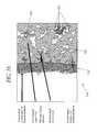
- FIG. 18is a magnified sectional view a surface portion of a filter material 134 in accordance with one embodiment.
- the filter material 134includes a large particle filtration layer 150 and a small particle filtration layer 152 .
- the large particle filtration layer 150preferably filters relatively larger particles, and the small particle filtration layer 152 preferably filters relatively smaller particles.
- the large particle filtration layer 150includes a plurality of voids 151 .
- the large particle filtration layer 150is about 20-60% void, and more preferably 30-50% void.
- the large particle filtration layer 150is about 42% void.
- the large particle filtration layer 150can comprise, for example, a stainless steel material.
- the large particle filtration layer 150preferably comprises a majority of the filter material 134 . Due to the voids 151 , the filter material 134 produces a relatively low pressure drop.
- One or more support tubes 154can be provided for enhanced structural rigidity of the large particle filtration layer 150 .
- the small particle filtration layer 152can have a pore size of 0.05-0.2 microns, and more preferably about 0.10 microns.
- the small particle filtration layer 152can have a thickness of about 5-20 microns, and more preferably about 10 microns.
- the small particle filtration layer 152may comprise, for example, a coating of Zirconia.
- Each side of the large particle filtration layer 150can be coated with a small particle filtration layer 152 .
- a suitable filter materialis one that is similar to an AccuSep filter sold by Pall Corporation.
- FIG. 19is a schematic illustration of a gas delivery system 160 that can be used to flow carrier and reactant gases through the precursor source vessel 100 and a vapor phase reaction chamber 162 .
- the delivery system 160includes the vessel 100 , a carrier gas source 164 , a downstream purifier or filter 166 , and several additional valves, as described herein.
- the isolation valves 108 , 110are preferably surface-mounted on the vessel 100 as described above.
- the carrier gas source 164is operable to deliver an inert carrier gas to a connection point 168 .
- a valve 170is interposed between the connection point 168 and the vessel inlet valve 108 .
- a valve 172is interposed between the connection point 168 and a connection point 174 .
- a valve 176is interposed between the connection point 174 and the vessel outlet valve 110 .
- the purifier 166 and an additional valve 178are interposed between the connection point 174 and the reaction chamber 162 .
- the vessel 100can have appropriate control and alarm interfaces, displays, panels, or the like.
- valves 170 , 108 , 110 , 176 , and 178are opened and the valve 172 is closed.
- the valves 172 and 178are opened, and preferably all of the valves 170 , 108 , 110 , and 176 are closed.
- the valve 178can be used to isolate the reaction chamber 162 from the gas delivery system 160 , e.g. for maintenance and repair.
- a precursor gas delivery system(such as that shown in FIG. 19 ) can be embodied in a gas interface assembly 180 that facilitates control of the flow of carrier gas and reactant vapor through the vessel 100 and an associated vapor phase reaction chamber.
- the illustrated gas interface assembly 180includes a plurality of valves 182 (which can perform substantially the same functions as the valves 170 , 172 , 176 , and 178 of FIG. 19 ), a downstream purifier or filter 184 , and a heater plate 186 .
- the valves 182can include valve porting blocks 188 similar in principle and operation to the valve porting blocks 118 and 120 .
- a gas line 133extends from one of the valves 182 that receives carrier gas from a carrier gas source 164 .
- the valve 182 from which the gas line 133 extendscan perform substantially the function of valve 170 of FIG. 19 .
- FIG. 7does not show the gas line extending into such a valve from the carrier gas source, but it will be understood to be provided.
- the gas line 133includes a fitting 131 that connects to the carrier gas inlet fitting 122 of the vessel 100 when the vessel and the gas interface assembly 180 are connected.
- An outlet 135 of the gas interface assembly 180delivers gas to a reaction chamber 162 .
- the source vessel's carrier gas inletcould be configured to be similar to the outlet orifice 128 .
- the heater plate 186heats up the valves 182 and the vessel 100 , preferably to a temperature above the vaporization temperature of the precursor.
- the heater plate 186can be heated by a variety of different types of heaters, such as cartridge heaters or line heaters.
- the heater platecan be formed of a variety of materials, such as aluminum, stainless steel, titanium, or various nickel alloys.
- Thermofoil-type heaterscan also be used to heat the heater plate 186 and valve porting blocks 188 .
- the use of a thermofoil-type heatercan allow variable watt density or more than one temperature control zone. Incorporation of variable watt density or multiple temperature control zones on the heater plate 186 can make it possible to induce a temperature gradient along the flow path of the gas. This can provide a gradual heating of the reactant vapor as it moves downstream, so that condensation is avoided.
- Suitable thermofoil heatersare sold by Minco of Minneapolis, Minn. Additional heaters (including line heaters, cartridge heaters, radiant heat lamps, and thermofoil-type heaters) can also be provided to heat the vessel lid 106 and container body 104 .
- a dedicated heatercan be provided to heat the vessel 100 .
- a dedicated heating device 220is provided beneath a lower surface of the vessel's container body 104 .
- precursor vaporcan also be drawn from the vessel 100 by the “vapor draw” and external gas flow methods.
- a vacuumis applied to the vessel 100 to draw out the vapor.
- the vacuumcan be applied downstream of the reaction chamber 162 , with the valves 110 , 176 , and 178 open and the valves 108 , 170 , and 172 closed.
- the vacuumcan be applied, for example, by using a vacuum pump.
- the precursor vaporcan be drawn from the vessel 100 by flowing the carrier gas from the source 164 to the reaction chamber 162 , with the valves 110 , 172 , 176 , and 178 open and the valves 108 and 170 closed. Under certain conditions, this can create a pressure differential between the vessel 100 and the flow path of the carrier gas, which causes the precursor vapor to flow toward the reaction chamber.
- the quick-connection assembly 102preferably facilitates quicker and easier loading, aligning, and connection of the precursor source vessel 100 to the gas interface assembly 180 .
- the quick-connection assembly 102is ergonomically friendly and facilitates replacement, recharging, and serviceability of the vessel 100 .
- a variety of different types of quick-connection assembliescan be provided, keeping in mind these goals, and skilled artisans will understand that the illustrated assembly 102 is merely one embodiment.
- the quick-connection assembly 102can be incorporated into the vacuum enclosure where the source vessel 100 and supporting control hardware are packaged.
- the illustrated quick-connection assembly 102includes a base 190 , a pedestal 192 extending upward from an edge of the base 190 , a track component 194 , and a lift assembly 196 .
- the base 190can preferably be secured to a lower inner surface of the gas delivery system 6 ( FIG. 1 ), such as on the floor 9 of the reactant source cabinet 16 .
- the pedestal 192is connected to and supports the gas interface assembly 180 at a position above the base 190 .
- the track component 194includes a platform 198 and two roller tracks 200 on opposite sides of the platform 198 .
- a pair of roller assemblies 202 having aligned rollers 204is preferably secured to opposite sides of the vessel 100 .
- the rollers 204are sized and configured to roll within the tracks 200 of the track component 194 , so that the vessel 100 can be easily and quickly positioned on the platform 198 .
- the outlet of the outlet valve 110is preferably vertically aligned with an inlet of one of the valves 182 of the gas interface assembly 180 .
- the lift assembly 196is configured to move the platform 198 vertically between lowered (shown in FIG. 7 ) and raised positions (shown in FIGS. 20-21 ).
- the outlet of the outlet valve 110preferably communicates, either directly or indirectly, with an inlet of one of the valves 182 .
- a minimal degree of manual adjustmentmay be required to suitably seal the interface between the outlet of the outlet valve 110 and the inlet of the valve 182 .
- the outlet of the outlet valve 110is an orifice 128 in the valve porting block 120 . In this manner, the quick-connection assembly 102 enables quick connection of the precursor source vessel 100 and the gas interface assembly 180 .
- the illustrated lift assembly 196comprises a lift handle 195 that can manually actuate scissor legs 197 to vertically move the platform 198 .
- the handle 195 and legs 197can operate in a manner that is similar to some existing auto jacks.
- the lift assembly 196lifts the platform 198 to its raised position when the handle 195 is rotated approximately 180°.
- other types of lift devicescan alternatively be provided.
- the quick-connection assembly 102makes it easier to exchange a depleted vessel 100 with a new vessel.
- the assembly 102simplifies vessel removal and installation, it is also easier to perform routine maintenance on the vessel 100 .
- the weight of the vessel 100is such that it can be easily managed by a single technician.
- FIGS. 22-24show an alternative embodiment of a quick-connection assembly 102 .
- the illustrated assembly 102includes the platform 198 and pedestal 192 .
- the platform 198includes tracks 200 adapted to receive tongues 206 attached on opposite sides of the vessel 100 .
- One or more lift devices 208are provided to raise the platform 198 .
- the lift devices 208comprise bolts underneath the platform 198 .
- the boltscan be turned to cause the platform 198 to rise to the connection position associated with the vessel 100 .
- a guide apparatus(not shown) can be provided to maintain the vertical alignment of the platform 198 .
- precursor source vesselsare typically supplied with a head pressure of inert gas (e.g., helium) in the vessel.
- inert gase.g., helium
- a head pressure of inert gase.g., helium
- solid precursor particlesbecome aerosolized and entrained in the inert gas outflow. This can contaminate the gas delivery system because such gas is typically vented out through the vessel's outlet isolation valve, the reactant gas delivery system, and ultimately the reactor's exhaust/scrubber. Later, during substrate processing, the contaminated portions of the gas panel that are common to the precursor delivery path and the vent path can cause processing defects during ALD on the substrate.
- FIG. 26shows an example of a precursor source vessel 100 that includes a vent valve 210 .
- the vent valve 210is positioned intermediate the inlet isolation valve 108 and the outlet isolation valve 110 .
- the vent valve 210includes a valve porting block 212 , which can be substantially similar to the valve porting blocks 118 and 120 .
- FIG. 27shows the vessel 100 of FIG. 26 connected to the gas interface assembly of FIGS. 22-24 , as described above.
- FIG. 28is a sectional view of an embodiment of the vessel 100 of FIG. 26 .
- the vessel 100includes a container body 104 , a serpentine insert 112 , a spring 114 , and a vessel lid 106 .
- the vessel lid 106includes the surface-mounted isolation valves 108 and 110 , as well as the preferably surface-mounted isolation valve 210 .
- the valves 108 , 210 , and 110include valve porting blocks 118 , 212 , and 120 , respectively.
- FIG. 28also shows internal gas passages 214 of the valve porting blocks.
- the valve porting block 120includes a gas outlet 128 that supplies the precursor vapor and carrier gas to the gas interface assembly 180 .
- a filteris preferably associated with each of the valves 108 , 210 , and 110 .
- the vessel lid 106includes a filter 130 (e.g., as shown in FIG. 17 and described above) associated with each valve. It will be appreciated that a variety of different types of filters can be used. The filters prevent precursor particles from exiting the vessel 100 .
Landscapes
- Chemical & Material Sciences (AREA)
- General Chemical & Material Sciences (AREA)
- Chemical Kinetics & Catalysis (AREA)
- Engineering & Computer Science (AREA)
- Materials Engineering (AREA)
- Mechanical Engineering (AREA)
- Metallurgy (AREA)
- Organic Chemistry (AREA)
- Chemical Vapour Deposition (AREA)
Abstract
Description
- The present application claims priority to U.S. Provisional Patent Application No. 60/850,886, filed Oct. 10, 2006 and claims priority to and is a continuation-in-part of application Ser. No. 11/870,374, filed Oct. 10, 2007.
- The present application relates generally to semiconductor processing equipment and specifically to apparatus for delivering reactant gases to processing chambers.
- Chemical vapor deposition (CVD) is a known process in the semiconductor industry for forming thin films of materials on substrates such as silicon wafers. In CVD, reactant gases (also referred to herein as “precursor gases”) of different reactants are delivered to one or more substrates in a reaction chamber. In many cases, the reaction chamber includes only a single substrate supported on a substrate holder (such as a susceptor), with the substrate and substrate holder being maintained at a desired process temperature. The reactant gases react with one another to form thin films on the substrate, with the growth rate being controlled either by the temperature or the amounts of reactant gases.
- In some applications, the reactant gases are stored in gaseous form in a reactant source vessel. In such applications, the reactant vapors are often gaseous at ambient (i.e., normal) pressures and temperatures. Examples of such gases include nitrogen, oxygen, hydrogen, and ammonia. However, in some cases, the vapors of source chemicals (“precursors”) that are liquid or solid (e.g., hafnium chloride) at ambient pressure and temperature are used. These source chemicals may have to be heated to produce sufficient amounts of vapor for the reaction process. For some solid substances (referred to herein as “solid source precursors”), the vapor pressure at room temperature is so low that they have to be heated to produce a sufficient amount of reactant vapor and/or maintained at very low pressures. Once vaporized, it is important that the vapor phase reactant is kept at or above the vaporizing temperature through the processing system so as to prevent undesirable condensation in the valves, filters, conduits, and other components associated with delivering the vapor phase reactants to the reaction chamber. Vapor phase reactants from such naturally solid or liquid substances are useful for chemical reactions in a variety of other industries.
- Atomic layer deposition (ALD) is another known process for forming thin films on substrates. In many applications, ALD uses a solid and/or liquid source chemical as described above. ALD is a type of vapor deposition wherein a film is built up through self-saturating reactions performed in cycles. The thickness of the film is determined by the number of cycles performed. In an ALD process, gaseous precursors are supplied, alternatingly and repeatedly, to the substrate or wafer to form a thin film of material on the wafer. One reactant adsorbs in a self-limiting process on the wafer. A different, subsequently pulsed reactant reacts with the adsorbed material to form a single molecular layer of the desired material. Decomposition may occur through reaction with an appropriately selected reagent, such as in a ligand exchange or a gettering reaction. In a typical ALD reaction, no more than a molecular monolayer forms per cycle. Thicker films are produced through repeated growth cycles until the target thickness is achieved.
- A typical solid or liquid source precursor delivery system includes a solid or liquid source precursor vessel and a heating means (e.g., radiant heat lamps, resistive heaters, etc.). The vessel includes the solid (e.g., in powder form) or liquid source precursor. The heating means heats up the vessel to increase the vapor pressure of precursor gas in the vessel. The vessel has an inlet and an outlet for the flow of an inert carrier gas (e.g., N2) through the vessel. The carrier gas sweeps precursor vapor along with it through the vessel outlet and ultimately to a substrate reaction chamber. The vessel typically includes isolation valves for fluidly isolating the contents of the vessel from the vessel exterior. Ordinarily, one isolation valve is provided upstream of the vessel inlet, and another isolation valve is provided downstream of the vessel outlet. Precursor source vessels are normally supplied with tubes extending from the inlet and outlet, isolation valves on the tubes, and fittings on the valves, the fittings being configured to connect to the gas flow lines of the remaining substrate processing apparatus. It is often desirable to provide a number of additional heaters for heating the various valves and gas flow lines between the precursor source vessel and the reaction chamber, to prevent the precursor gas from condensing and depositing on such components. Accordingly, the gas-conveying components between the source vessel and the reaction chamber are sometimes referred to as a “hot zone” in which the temperature is maintained above the vaporization/condensation temperature of the precursor.
- It is known to provide a serpentine or tortuous flow path for the flow of carrier gas while it is exposed to a solid or liquid precursor source. For example, U.S. Pat. Nos. 4,883,362; 7,122,085; and 7,156,380 each disclose such a serpentine path.
- In an aspect of the present invention, a precursor source vessel is provided. The precursor source vessel includes a lid having an inlet port, an outlet port, and a burp port. The precursor source vessel further includes a base removably attached to the lid. The base includes a recessed region formed therein.
- In another aspect of the present invention, a precursor source vessel is provided. The precursor source vessel includes a base having a recessed region formed therein. The recessed region is configured to receive a precursor material. The precursor source vessel also includes a lid removably attached to the base. The lid has an inlet port, an outlet port, and a burp port. A burp valve is operatively attached to the lid. The burp valve is operatively connected to the burp port.
- In yet another aspect of the present invention, a precursor source vessel is provided. The precursor source vessel includes a base having a bottom surface, a contact surface, a side surface extending between the contact and bottom surfaces, and an inner surface extending from the contact surface to define a recessed region within the base. The precursor source vessel also includes a lid removably attached to the base. The lid includes an inlet port, an outlet port, and a burp port.
- In still another aspect of the present invention, a precursor source vessel is provided. The precursor source vessel includes a lid having a first port, a second port, and a third port. The precursor source vessel also includes a base removably attached to the lid. The base includes a recessed region formed therein.
- In still another aspect, an apparatus for connecting a chemical reactant source vessel to a gas interface assembly of a vapor phase reactor for vapor processing of substrates is provided. The apparatus comprises a vessel, a gas interface assembly of a vapor phase reactor, and a connection assembly for connecting the vessel to the gas interface assembly. The vessel has a chamber adapted to contain a solid or liquid chemical reactant. The vessel includes an inlet and an outlet in fluid communication with the chamber. The gas interface assembly has a gas inlet adapted to connect to the outlet of the vessel chamber. The connection assembly comprises a track component and a lift assembly. The track component includes one or more elongated tracks adapted to movably engage one or more track engagement members of the vessel. The lift assembly is configured to move the track component vertically between a lowered position and a raised position. When the vessel's one or more track engagement members engage the one or more tracks of the track component, and when the lift assembly moves the track component to its raised position, the vessel's outlet becomes positioned to substantially directly fluidly communicate with the gas inlet of the gas interface assembly.
- For purposes of summarizing the invention and the advantages achieved over the prior art, certain objects and advantages of the invention have been described herein above. Of course, it is to be understood that not necessarily all such objects or advantages may be achieved in accordance with any particular embodiment of the invention. Thus, for example, those skilled in the art will recognize that the invention may be embodied or carried out in a manner that achieves or optimizes one advantage or group of advantages as taught herein without necessarily achieving other objects or advantages as may be taught or suggested herein.
- All of these embodiments are intended to be within the scope of the invention herein disclosed. These and other embodiments of the present invention will become readily apparent to those skilled in the art from the following detailed description of the preferred embodiments having reference to the attached figures, the invention not being limited to any particular preferred embodiment(s) disclosed.
- These and other aspects of the invention will be readily apparent to the skilled artisan in view of the description below, the appended claims, and from the drawings, which are intended to illustrate and not to limit the invention, and wherein:
FIG. 1 is a schematic illustration of a conventional precursor source assembly and a reactor chamber assembly.FIG. 2 is a perspective view of a conventional solid precursor source vessel.FIG. 3 is an illustration of both ideal and less than ideal source chemical concentrations in reactant gas pulses for atomic layer deposition.FIG. 4 is a schematic illustration of a conventional precursor source vessel and gas panel.FIG. 5 is a schematic illustration of a precursor source vessel with surface-mounted valves and a gas panel.FIG. 6 is a schematic illustration of a precursor source vessel with surface-mounted valves and a gas panel in close thermal contact with the vessel.FIG. 7 is a perspective view of an embodiment of a precursor source vessel, a gas interface assembly for fluidly communicating with the vessel, and a quick-connection assembly for connecting and disconnecting the vessel to the gas interface assembly.FIG. 8 is an exploded perspective view of the vessel ofFIG. 7 .FIG. 9 is a rear perspective sectional view of the vessel ofFIG. 7 .FIG. 10 is a rear sectional view of the vessel ofFIG. 7 .FIG. 11A is an exploded view of another embodiment of a precursor source vessel.FIG. 11B is a top perspective view of a lid for the precursor source vessel shown inFIG. 11A .FIG. 11C is a bottom perspective view of the lid shown inFIG. 11B .FIG. 11D is a top perspective view of an embodiment of a base for the precursor source vessel shown inFIG. 11A .FIG. 11E is a top plan view of the base shown inFIG. 11D .FIG. 11F is a cross-sectional view of the base shown inFIG. 11E taken along line A-A.FIG. 11G is a cross-sectional view of the base shown inFIG. 11E taken along line B-B.FIG. 11H is a cross-sectional view of another embodiment of a base for the precursor source vessel shown inFIG. 11A .FIG. 11I is a top plan view of yet another embodiment of a base for the precursor source vessel shown inFIG. 11A .FIG. 11J is an exploded perspective view of another embodiment of a source vessel.FIG. 12 is an exploded perspective view of an embodiment of a serpentine insert comprising a stack of trays.FIG. 13 is a perspective view of an upper stacking tray of the serpentine insert ofFIG. 12 .FIG. 14 is a top view of the upper stacking tray ofFIG. 13 .FIG. 15 is a perspective view of a lower stacking tray of the serpentine insert ofFIG. 12 .FIG. 16 is a top view of the lower stacking tray ofFIG. 15 .FIG. 17 is a sectional view of a filter mounted on a lid of a precursor source vessel.FIG. 18 is an embodiment of a filter material that can be used for the filter ofFIG. 17 .FIG. 19 is a schematic illustration of a gas delivery system for flowing carrier and reactant gases through a precursor source vessel and a vapor phase reaction chamber.FIGS. 20 and 21 are front perspective views of the vessel and gas interface assembly ofFIG. 7 , shown connected.FIG. 22 is a top front perspective view of the precursor source vessel and gas interface assembly ofFIG. 7 , with an alternative embodiment of a quick-connection assembly.FIG. 23 is a top front perspective view of the vessel and gas interface assembly ofFIG. 22 , shown connected.FIG. 24 is a bottom front perspective view of the vessel and gas interface assembly ofFIG. 22 , shown separated.FIG. 25 is a schematic illustration of a gas delivery system for flowing carrier and reactant gases through a precursor source vessel and a reaction chamber.FIG. 26 is a perspective view of a precursor source vessel with a vent valve.FIG. 27 is a perspective view of the vessel ofFIG. 26 connected to the gas interface assembly ofFIGS. 22-24 .FIG. 28 is a sectional view of the vessel ofFIG. 26 , with the addition of a dedicated heating device for the vessel.- The present application for letters patent discloses improved precursor source vessels, apparatuses and methods for loading and connecting the vessels to a reactor, and interfaces for using the vessels with vapor processing reactors. The disclosed embodiments provide excellent access to reactant vapor, reduced contamination of the reactor's gas delivery system, and improved serviceability (e.g., replacement or recharging) of the precursor source vessel.
- The following detailed description of the preferred embodiments and methods details certain specific embodiments to assist in understanding the claims. However, one may practice the present invention in a multitude of different embodiments and methods, as defined and covered by the claims.
FIG. 1 schematically illustrates a conventionalprecursor delivery system 6 for feeding a gas phase reactant generated from a solid or liquidprecursor source vessel 10 into a gasphase reaction chamber 12. Skilled artisans will understand that the precursor delivery systems of the present invention may incorporate many of the aspects of thegas delivery system 6 ofFIG. 1 . Accordingly, theconventional delivery system 6 is now described in order to better understand the invention.- With reference to
FIG. 1 , the solid orliquid source vessel 10 contains a solid or liquid source precursor (not shown). A solid source precursor is a source chemical that is solid under standard conditions (i.e., room temperature and atmospheric pressure). Similarly, a liquid source precursor is a source chemical that is liquid under standard conditions. The precursor is vaporized within thesource vessel 10, which may be maintained at or above a vaporizing temperature. The vaporized reactant is then fed into thereaction chamber 12. Thereactant source vessel 10 and thereaction chamber 12 can be located in areactant source cabinet 16 and areaction chamber vessel 18, respectively, which are preferably individually evacuated and/or thermally controlled. This can be achieved by providing these components with separate cooling and heating devices, insulation, and/or isolation valves and associated piping, as known in the art. - The illustrated
gas delivery system 6 is particularly suited for delivering vapor phase reactants to be used in a vapor phase reaction chamber. The vapor phase reactants can be used for deposition (e.g., CVD) or Atomic Layer Deposition (ALD). - As seen in
FIG. 1 , thereactant source vessel 10 and thereaction chamber 12 are adapted to be in selective fluid communication with each other through afirst conduit 20 so as to feed the gas phase reactant from thereactant source vessel 10 to the reaction chamber12 (such as an ALD reaction chamber). Thefirst conduit 20 includes one ormore isolation valves 22a,22b, which may be used for separating the gas spaces of thereactant source vessel 10 and thereaction chamber 12 during evacuation and/or maintenance of either or both of thereactant source vessel 10 and thereaction chamber vessel 18. - Inactive or inert gas is preferably used as a carrier gas for the vaporized precursor. The inert gas (e.g., nitrogen or argon) may be fed into the
precursor source vessel 10 through asecond conduit 24. Thereactant source vessel 10 includes at least one inlet for connection to thesecond conduit 24 and at least one outlet for withdrawing gas from thevessel 10. The outlet of thevessel 10 is connected to thefirst conduit 20. Thevessel 10 can be operated at a pressure in excess of the pressure of thereaction chamber 12. Accordingly, thesecond conduit 24 includes at least oneisolation valve 26, which can be used for fluidly isolating the interior of thevessel 10 during maintenance or replacement of the vessel. Acontrol valve 27 is preferably positioned in thesecond conduit 24 outside of thereactant source cabinet 16. - In another variation (which can be employed in embodiments of the present invention), the precursor vapor can be drawn to the
reaction chamber 12 by applying a vacuum to thereactant source vessel 10, without using a carrier gas. This is sometimes referred to as “vapor draw.” - In yet another variation (which can also be employed in embodiments of the present invention), the precursor vapor can be drawn out of the
vessel 10 by an external gas flow that creates a lower pressure outside of the vessel, as in a Venturi effect. For example, the precursor vapor can be drawn by flowing a carrier gas toward thereaction chamber 12 along a path downstream of thevessel 10. Under some conditions, this can create a pressure differential between thevessel 10 and the flow path of the carrier gas. This pressure differential causes the precursor vapor to flow toward thereaction chamber 12. - In order to remove dispersed solid particles when a solid source precursor is used, the
gas delivery system 6 includes apurifier 28 through which the vaporized reactant is conducted. Thepurifier 28 may comprise one or more of a wide variety of purifying devices, such as mechanical filters, ceramic molecular sieves, and electrostatic filters capable of separating dispersed solids or particles or molecules of a minimum molecular size from the reactant gas flow. It is also known to provide an additional purifier in thevessel 10. In particular, U.S. Published Patent Application No. US 2005/0000428A1 discloses a vessel comprising a glass crucible enclosed within a steel container, the crucible containing the reactant source and having a lid with a filter. The lid is separate from a vessel lid that attaches to the steel container. - With continued reference to
FIG. 1 , thereactant source vessel 10 is positioned within thereactant source cabinet 16. Theinterior space 30 of thecabinet 16 can be kept at a reduced pressure (e.g., 1 mTorr to 10 Torr, and often about 500 mTorr) to promote radiant heating of the components within thecabinet 16 and to thermally isolate such components from each other to facilitate uniform temperature fields. In other variations, the cabinet is not evacuated and includes convection-enhancing devices (e.g., fans, cross-flows, etc.). The illustratedcabinet 16 includes one ormore heating devices 32, such as radiation heaters. Also,reflector sheets 34 can be provided, which may be configured to surround the components within thecabinet 16 to reflect the radiant heat generated by theheating devices 32 to the components positioned within thecabinet 16.Reflector sheets 34 can be provided on theinner walls 40 of thecabinet 16, as well as on the cabinet's ceiling7 andfloor 9. In the illustrated apparatus, a substantial length of thefirst conduit 20 is contained within thereactant source cabinet 16. Thus thefirst conduit 20 will inherently receive some heat to prevent condensation of reactant vapors. - The
reactant source cabinet 16 can include a coolingjacket 36 formed between anouter wall 38 and aninner wall 40 of the cabinet. The coolingjacket 36 can contain water or another coolant. Thejacket 36 allows theouter surface 38 of thecabinet 16 to be maintained at or near ambient temperatures. - In order to prevent or reduce gas flow from the
reactant source vessel 10 between the alternating pulses of an ALD process, it is possible to form an inactive gas barrier in thefirst conduit 20. This is also sometimes referred to as “inert gas valving” or a “diffusion barrier” in a portion of thefirst conduit 20 to prevent flow of reactant from thereactant source vessel 10 to thereaction chamber 12 by forming a gas phase barrier by flowing gas in the opposite direction to the normal reactant flow in thefirst conduit 20. The gas barrier can be formed by feeding inactive gas into thefirst conduit 20 via athird conduit 50 connected to theconduit 20 at aconnection point 52. Thethird conduit 50 can be connected to aninert gas source 54 that supplies thesecond conduit 24. During the time intervals between the feeding of vapor-phase pulses from thereactant source vessel 10, inactive gas is preferably fed into thefirst conduit 20 through thethird conduit 50. This gas can be withdrawn via afourth conduit 58, which is connected to thefirst conduit 20 at asecond connection point 60 located upstream of the first connection point52 (i.e., closer to the reactant source vessel10). In this manner, an inert gas flow of an opposite direction to the normal reactant gas flow is achieved (between reactant pulses) in thefirst conduit 20 between the first and second connection points52,60. Thefourth conduit 58 can be in communication with an evacuation source64 (such as a vacuum pump). Arestriction 61 andvalves gas delivery system 6 are illustrated and described in U.S. Published Patent Application No. US 2005/0000428A1. - Existing solid or liquid precursor source delivery systems, such as the
system 6 shown inFIG. 1 , have a number of drawbacks and limitations. One drawback is that it is sometimes necessary to provide a large number of additional heaters to heat up the gas lines and valves between the precursor source vessel (such as the vessel10) and the reaction chamber (such as the reaction chamber12). In particular, it is normally desirable to maintain all of these intervening gas-conveying components (e.g., thevalves purifier 28, conduit20) at a temperature above the condensation temperature of the precursor, to prevent the precursor vapor from depositing on such components. Typically, these intervening components are heated separately by line heaters, cartridge heaters, heat lamps, and the like. Some systems (e.g., U.S. Published Patent Application No. 2005/0000428A1) utilize these additional heaters to bias the intervening components to a temperature above that of the source vessel. Such temperature biasing helps to prevent precursor condensation in the intervening components during cool-down. Since the source vessel typically has a higher thermal mass than the intervening gas-conveying components, these components are at risk of cooling down to the condensation temperature faster than the source vessel. This can lead to an undesirable condition in which the source vessel is still producing precursor vapor that can flow to the cooler intervening components and deposit thereon. The temperature biasing can overcome this problem. However, the need for additional heaters increases the total size and operating cost of the apparatus. - Further, conventional solid source delivery systems typically employ filters (such as the
purifier 28 ofFIG. 1 ) between the source vessel outlet and the substrate reaction chamber, in order to prevent solid precursor particles (e.g., powder entrained in the carrier gas flow) from entering the reaction chamber. Such filters also add to the total size of the apparatus and can require additional heaters to prevent condensation therein. Also, such filters are typically downstream of the source vessel outlet, which involves a risk that precursor particles may deposit on gas-conveying components downstream of the vessel outlet, such as within gas conduits or within the vessel outlet valve itself. These particles can damage components such as valves, which can compromise their ability to completely seal. - Another drawback of conventional solid or liquid source delivery systems is that it is often difficult to recharge or replace the precursor source vessel.
FIG. 2 shows a typicalprecursor source vessel 31 comprising acontainer body 33 and alid 35. Thelid 35 includesinlet tubes 43a,43bandoutlet tubes isolation valve 37 is interposed between theinlet tubes 43a,43b, and anisolation valve 39 is interposed between theoutlet tubes isolation valve 41 is interposed between gas lines connecting thetubes 43aand45a. Theinlet tubes 43a,43bandoutlet tubes container body 33. Thetubes 43a,45atypically includefittings 47 configured to connect to other gas flow lines of the reactant gas delivery system. When the solid or liquid source precursor is depleted and in need of replacement, it is customary to replace theentire source vessel 31 with a new one that has a full load of the source chemical. Replacing thesource vessel 31 requires shutting off theisolation valves fittings 47 from the remaining substrate processing apparatus, physically removing thevessel 31, placing anew vessel 31 in the appropriate location, and connecting thefittings 47 of thenew vessel 31 to the remaining substrate processing apparatus. Often, this process also involves disassembling various thermocouples, line heaters, clamps, and the like. These processes can be somewhat laborious. - Another drawback of conventional solid or liquid source delivery systems is that the gas delivery system can produce areas of stagnant flow (also referred to as “dead legs”). Dead legs tend to occur when the gas flow path from the precursor source vessel is longer and more complex. Conventional inlet and outlet isolation valves for the source vessel (as described above) can produce dead legs. In general, dead legs increase the risk of unwanted precursor deposition on the gas-conveying components of the delivery system. Such unwanted precursor deposition can occur due to cold spots associated with the dead volumes, wherein the precursor solidifies at temperatures below the sublimation/melting temperature. Such unwanted precursor deposition can also occur due to hot spots associated with the dead volumes, wherein the precursor decomposes at high temperatures. For this reason, it is generally desirable to reduce and minimize stagnation of the reactant gas flow. It is also generally desirable to reduce the surface area to be temperature-controlled, in order to lessen the chance of producing hot or cold spots.
- Another reason to minimize the amount and volume of dead legs is to reduce the total volume of the gas delivery system interposed between the precursor source vessel and the substrate reaction chamber. As the total volume of the gas delivery system increases, often times the minimum pulse time and minimum purge time associated with ALD processing increase as well. The minimum pulse time is the pulse time necessary for an injected reactant to saturate the surface of a substrate being processed. The minimum purge time is the time necessary to purge excess reactant from the substrate reaction chamber and gas delivery system between reactant pulses. Substrate throughput (the rate at which substrates can be processed) is increased when the minimum pulse time and minimum purge time are decreased. Accordingly, it is desirable to reduce the amount and volume of dead legs in order to increase throughput.
- Another benefit of reducing the total volume of the gas delivery system is to improve the “pulse shape” of the reactant gas pulses. The pulse shape refers to the shape of a curve of the reactant's chemical concentration in the reactant/carrier mixture, for a reactant gas pulse.
FIG. 3 shows an example of an idealreactant concentration curve 80, as well as acurve 82 that is less than ideal. Both curves includereactant gas pulses 84 separated bytime periods 86 of substantially zero reactant concentration. Theideal curve 80 resembles a rectilinear wave, such as a square wave. A substantially rectilinear wave is preferred because it is highly desirable for each reactant gas pulse to deliver the reactant species to all of the available reaction sites on the substrate surface (saturation) in the least amount of time, in order to optimize substrate throughput. A rectilinear pulse shape, as in thecurve 80, optimizes throughput because the duration of each pulse has a high concentration of the reactant, which in turn reduces the pulse duration necessary to deliver sufficient reactant species to the substrate surface. Also, the reduced dispersion of a rectilinear pulse shape reduces the amount of “pulse overlap” between successive pulses of different precursors, which reduces the potential for unwanted CVD growth modes. In contrast, the pulse concentration of eachpulse 84 of thenon-ideal curve 82 takes longer to reach its maximum level, which increases the pulse duration necessary to fully saturate the substrate surface. Thus, the frequency of thecurve 80 is less than that of thecurve 82. As the total volume of the gas delivery system increases, the pulse shape deteriorates. Accordingly, it is desirable to improve the pulse shape (i.e., make it more like a square wave) by minimizing dead legs. - Another drawback of conventional solid source delivery systems is the risk of contamination involved in venting the precursor source vessel prior to processing. Precursor source vessels are typically supplied with a head pressure of gas in the vessel. For example, a source vessel filled with precursor powder is often shipped with helium or other inert gas at a pressure slightly higher (e.g., 5 psi) than ambient pressure. Helium is typically used to enable an “out-bound” helium leak test using a helium leak detector to ensure vessel integrity just prior to shipment. This helium is often left or replaced with N2or other inert gas so that if a small leak is present, the gas leaks outward from the vessel, preventing atmospheric contamination of the precursor within the vessel. Before the vessel is used in substrate processing, the head pressure of internal gas is ordinarily removed. Typically, the vessel's internal gas is vented out through the vessel's outlet isolation valve, through the reactant gas delivery system, and ultimately through the reactor's exhaust/scrubber. In some systems, the vessel's internal gas is vented out through the substrate reaction chamber. Other systems employ a gas line in parallel with the reaction chamber (i.e., extending from a point just upstream of the reaction chamber to a point just downstream of the reaction chamber), such that the vessel's internal gas can be directed to the exhaust/scrubber without flowing through the reaction chamber. In either case, current vessel designs involve a risk of particle generation when the vessel is relieved of the head pressure. This can result in precursor powder becoming entrained within the vent flow (i.e., the venting out of the internal pressurized gas of the vessel), which can contaminate and possibly damage downstream components of the gas delivery system, including the vessel outlet itself. Even during normal processing, precursor material (e.g., powder) can become entrained within the carrier gas flowing through the precursor source vessel, which involves a risk of unwanted deposition of the precursor within the gas delivery system.
- The presently disclosed embodiments of precursor delivery systems substantially overcome these problems by employing an improved precursor source vessel and apparatus for quickly connecting and disconnecting the vessel from the rest of the delivery system. These aspects are now described.
- Gas Panel in Close Thermal Contact with Source Vessel
FIGS. 4-6 illustrate three different gas panel arrangements. A gas panel typically includes one or more valves that are downstream of a precursor source vessel, and can also include one or more valves upstream of the vessel.FIG. 4 illustrates a conventional arrangement in which a source chemical is contained within asource vessel 10. Agas panel 90 includes a plurality of valves operable to deliver carrier gas from a carrier gas source (not shown) through thevessel 10 and into a reaction chamber (not shown). An inlet valve91 is connected upstream of thevessel 10 bytubing 93, and anoutlet valve 92 is connected downstream of thevessel 10 bytubing 94. In this conventional arrangement, the inlet valve91, theoutlet valve 92, and the valves and tubing of thegas panel 90 are typically not in close thermal contact with thevessel 10.FIG. 5 illustrates an arrangement that is somewhat improved relative to that ofFIG. 4 . In the arrangement ofFIG. 5 , aprecursor source vessel 100 has a surface-mountedinlet valve 108 and a surface-mountedoutlet valve 110. Thevalves conventional gas panel 90 bytubing valves vessel 100, but the valves and tubing of thegas panel 90 are not.FIG. 6 illustrates an arrangement that is improved relative to that ofFIG. 5 . In the arrangement ofFIG. 6 , thesource vessel 100 has a generally flat upper surface with a surface-mountedinlet valve 108 and a surface-mountedoutlet valve 110. Also, agas panel 97 is arranged such that the valves and tubing of the gas panel are positioned along a plane that is generally parallel to the generally flat surface of thevessel 100. In order to increase thermal contact between thevessel 100 and the gas panel valves and tubing, the distance between the plane of the gas panel valves and tubing and the generally flat surface of thevessel 100 is preferably no more than about 10.0 cm, more preferably no more than about 7.5 cm, and even more preferably no more than about 5.3 cm.- Source Vessel with Surface Mounted Valves and Serpentine Pathway
FIG. 7 shows an embodiment of an improved solid or liquidprecursor source vessel 100 and a quick-connection assembly 102. Thesource vessel 100 includes acontainer body 104 and alid 106. Thelid 106 includes surface-mountedisolation valves FIGS. 8-10 show thesource vessel 100 ofFIG. 7 in greater detail.FIG. 8 is an exploded view, andFIGS. 9 and 10 are rear cross-sectional views, of thesource vessel 100. The illustratedvessel 100 includes thecontainer body 104, aserpentine pathway insert 112 within thebody 104, and thelid component 106. The illustrated assembly is fastened together by fasteningelements 124, such as screws or nut and bolt combinations. Thefastening elements 124 are adapted to extend into aligned holes within aflange 126 of thebody 104. Skilled artisans will appreciate that the assembly can be fastened together by a variety of alternative methods.- The
serpentine pathway insert 112 preferably defines a tortuous orserpentine pathway 111 through which a carrier gas must travel as it flows through thevessel 100. Theserpentine pathway 112 preferably contains the precursor source, such as a powder or liquid. Theserpentine pathway 111 is significantly longer than the carrier gas flow pathway within conventional precursor source vessels. Thevalves 108 and110 (described below) and the valve210 (described below with reference toFIGS. 26-28 ) are subjected to a less severe environment, thereby increasing their reliability. - A
spring 114 is preferably provided to bias theserpentine insert 112 against thelid 106, to prevent the escape of reactant gas through the interface between theinsert 112 and thelid 106. In other words, thespring 114 tends to reduce the risk of the gas bypassing some or all of the serpentine path.Suitable springs 114 include flat wire compression springs, such as the Spirawave® wave springs sold by Smalley Steel Ring Company of Lake Zurich, Ill. FIG. 11A shows another embodiment of an improved solid or liquidprecursor source vessel 400 that includes acontainer base 402, aseal 404, and alid 406. Thelid 406 includes a plurality of integrated gas valves, or surface-mounted valves, described in more detail below.FIGS. 11B-11C illustrate an exemplary embodiment of thelid 406.FIGS. 11D-11G show an embodiment of thebase 402 of thesource vessel 400.FIGS. 11H-11I show other embodiments of thebase 402 of thesource vessel 400.- As shown in
FIG. 11A , thebase 402 is formed of a solid member that includes a recessedregion 408 that is machined directly into thesolid base 402. When thelid 406 is removably attached to thebase 402, aseal 404 is disposed therebetween prior to thelid 406 being secured to the base402 to ensure the contents within thesource vessel 400 are secured therewithin. In an embodiment, thebase 402 and thelid 406 are formed of the same material such that both members have substantially the same thermal conductivity and the same coefficient of thermal expansion therebetween. In another embodiment, thebase 402 is formed of a material different than the material used to form thelid 406. In an embodiment, thebase 402 and thelid 406 are formed of stainless steel. In other embodiments, thebase 402 and/orlid 406 may be formed of high nickel alloys, aluminum, or titanium. It should be understood by one of ordinary skill in the art that thebase 402 and thelid 406 can be formed of any other material sufficient to allow sufficient thermal heat transfer to vaporize the precursor disposed within thesource vessel 400 while being inert, or not reacting with the precursor or contents within thesource vessel 400. - A
seal 404 is disposed between the base402 and thelid 406 of thesource vessel 400, as shown inFIG. 11A . In an embodiment, theseal 404 is an o-ring that is disposed within agroove 410 formed in thebase 402. In another embodiment, theseal 404 can be formed as a metal gasket or a v-seal that is configured to be disposed between the base402 and thelid 406. It should be understood by one of ordinary skill in the art that theseal 404 can be formed of any shape, size, or configuration sufficient to provide a seal when thelid 406 is attached to thebase 402 and to ensure that the contents within thesource vessel 400 are secured therewithin. In an embodiment, theseal 404 is formed of an elastomer, but it should be understood by one of ordinary skill in the art that theseal 404 may be formed of any other material sufficient to provide a seal, such as, but not limited to, polymer or metal. - As illustrated in
FIGS. 11A-11C , an embodiment of alid 406 of asource vessel 400 is shown. Thelid 406 is formed as a single member having anupper surface 412, alower surface 414, and aside surface 413 extending between the upper andlower surfaces lower surfaces lower surfaces lower surfaces lid 406 with a consistent thickness T1across theentire lid 406. As shown inFIG. 11B , theupper surface 412 may include high-tolerance areas 416 that are machined so as to provide a substantially smooth area relative to the rest of theupper surface 412. These high-tolerance areas 416 allow thevalve assemblies 418 to be mounted flush with theupper surface 412 of thelid 406 to ensure as much direct thermal contact between thevalve assemblies 418 and thelid 406. With more surface area contact between these components, the heat transfer between these components can be maximized, thereby reducing the need for separate heaters or heating jackets to provide heat to thevalve assemblies 418 which prevents condensation of vaporized precursor therewithin. - As shown in
FIG. 11B , thelid 406 includes aninlet port 420, anoutlet port 422, and aburp port 424. Theinlet port 420 is configured to allow a carrier gas, or an inert gas, to be introduced into thesource vessel 400 therethrough. Theoutlet port 422 is configured to allow gases to exit thesource vessel 400 therethrough. Theburp port 424 may comprise any port, such as a conventional inlet/outlet port, that may be configured to relieve head pressure within thesource vessel 400 after either the initial fill and installation of thesource vessel 400 or after subsequent re-fills and installations of thesource vessel 400. The release of head pressure through theburp port 424 is done prior to thesource vessel 400 providing vaporized precursor material to the reaction chamber162 (FIG. 25 ) for semiconductor substrate processing. In an embodiment, aninterface component 426 is operatively attached to theupper surface 412 of thelid 406 at each of theports interface component 426 is configured to be connected to avalve assembly 418. It should be understood by one of ordinary skill in the art that eachvalve assembly 418 and aninterface component 426 may be operatively connected to theupper surface 412 of thelid 406 in any manner. - As illustrated in
FIGS. 11A and 11C , one of thevalve assemblies 418 includes a vent valve, orburp valve 428 that is operatively connected to theupper surface 412 of thelid 406. Theburp valve 428 can be a pneumatic valve or any other valve that regulates the flow of gases into and out of thesource vessel 400. In an embodiment, theburp valve 428 remains closed except when opened for release of gases to relieve the head pressure within thesource vessel 400 prior to use of thesource vessel 400 in a semiconductor processing system. During manufacture and initial filling of thesource vessel 400 with precursor, or after thesource vessel 400 is refilled with precursor, an inert gas is introduced into thesource vessel 400 so as to create a head pressure within thesource vessel 400. This head pressure is used to allow a leak check to be performed once thesource vessel 400 is filled (or refilled), as explained above. When thesource vessel 400 is being installed, the gases within thesource vessel 400 that create the head pressure need to be removed and replaced with the inert carrier gas that will be used to carry the vaporized precursor during processing. Historically, the head pressure was relieved from source vessels commonly known in the art by exhausting the gases creating the initial head pressure through an outlet port which is the same outlet port through which vaporized precursor material exits during processing of a substrate. However, a filter adjacent to the outlet port would often become clogged by precursor particles that accompanied the gases during an initial “burp” process or release. Although some of the precursor particles were stopped by the outlet filter, some particles are able to bypass the filter—or particles caught by the filter would subsequently become dislodged—and enter into the tubing that leads to the reaction chamber. These errant precursor particles can cause non-uniform deposition within the reaction chamber or clog the gas lines between the source vessel and the reaction chamber. The errant particles may also cause particle entrainment on the semiconductor substrate being processed, thereby resulting in a reduction of the number of devices, chips, or circuits that the substrate can produce. Theburp port 424 andcorresponding burp valve 428 of the present invention allow the head pressure to be relieved during a “burp” process in which the gases and particles exiting theburp port 424 are first filtered by aburp filter 430 before being diverted through aburp gas line 432 that is connected directly to the exhaust line466 (FIG. 25 ), thereby bypassing thereaction chamber 162 so as to prevent any unwanted particles from interfering with processing within thereaction chamber 162. - As shown in
FIG. 11C , afiltration apparatus 434 is operatively connected to thebottom surface 414 of thelid 406. Afiltration apparatus 434, as shown in greater detail inFIG. 18 and described below, is configured to filter the carrier gas being introduced through thelid 406 into thesource vessel 400 as well as the gases exiting thesource vessel 400 through theburp port 424 and theoutlet port 422. In the illustrated embodiment, afiltration apparatus 434 is attached to the underside of thelid 406 adjacent to theinlet port 420, theoutlet port 422, and theburp port 424. Thefiltration apparatuses 434 are attached directly to thelid 406 to allow a sufficient amount of heat transfer from thelid 406 to prevent condensation of precursor material within eachfiltration apparatus 434. Eachfiltration apparatus 434 preferably has a low-profile, because a low-profile filtration apparatus provides good thermal uniformity across the filter pack media (FIG. 17 ). - An embodiment of a
base 402 is shown inFIGS. 11E-11G . Thebase 402 includes abody 436 and aflange 438 that is integrally connected to thebody 436 and extends therefrom. In an embodiment, thebody 436 and theflange 438 are formed from a single piece of material. As explained above, agroove 410 is formed into thebody 436, wherein thegroove 410 is configured to receive theseal 404. Theflange 438 is configured to extend radially outward from the upper portion of thebody 436. Thebase 402 is defined by an upper,contact surface 440, abottom surface 442, aside surface 444, and aninner surface 446 that defines and forms the recessedregion 408. Thecontact surface 440 is a substantially planar surface that forms the entire upper surface of thebase 402. Thecontact surface 440 is configured to directly contact thelower surface 414 of thelid 406. - In an embodiment, the
base 402 is a solid piece of material or metal into which the recessedregion 408 is machined, or removed, as illustrated inFIGS. 11D-11G . In another embodiment, thebase 402 is formed as a one-piece casting in which the recessedregion 408 is formed into the base402 during the casting or forging process. The recessedregion 408 is configured to receive a solid or liquid precursor therewithin. In the embodiments shown inFIGS. 11D-11I , the recessedregion 408 is formed as an elongated, tortuous pathway extending from thecontact surface 440 of thebase 402. Theinner surface 446 extends from thecontact surface 440 into the thickness of thebody 436. The depth that the recessedregion 408 is formed into thebody 436 may vary. It should be understood by one of ordinary skill in the art that the shape, depth, and width of the recessedregion 408 may vary so long as the recessedregion 408 allows for an extended flow path between the inlet andoutlet ports region 408. - In an embodiment, as shown in
FIGS. 11E-11G , the recessedregion 408 includes an inlet recessedpad 448, an outlet recessedpad 450, a burp recessedpad 452, and achannel 454 that fluidly connects the recessedpads pads contact surface 440 of thebase 402. The shape of the recessedpads corresponding filtration apparatus 434 that extends from thelower surface 414 of thelid 406 into the base402 such that a portion of eachfiltration apparatus 434 is received within a corresponding recessedpad pads contact surface 440 to a predefined depth. In an embodiment, the depth of all of the recessedpads pads base 402 is filled with precursor, the volume within each of the recessedpads filtration apparatus 434 adjacent to theinlet port 420 of thelid 406, the carrier gas contacts and is distributed within the inlet recessedpad 448 before traveling throughout the remainder of the recessedregion 408. Because there is preferably no precursor located within any of the recessedpads pad 448 prevents the carrier gas from directly contacting the precursor and potentially stifling up the precursor or causing particles of the precursor to be intermixed with the carrier gas. Each of the recessedpads region 408 is fluidly connected by way of thechannel 454 formed into thebody 436. - As illustrated in
FIGS. 11F-11G , thechannel 454 of the recessedregion 408 extends from thecontact surface 440, wherein thechannel 454 is a continuous pathway along which gases can travel between the inlet recessedpad 448 and the outlet recessedpad 450. In another embodiment, the recessedregion 408 does not include recessed pads such that thechannel 454 extends the entire distance between thefiltration apparatus 434 adjacent to theinlet port 420 and thefiltration apparatus 434 adjacent to the outlet and burpports channel 454 is formed into thebody 436 such that thechannel 454 has a depth that is greater than the depth of the recessedpads channel 454 is constant along the entire length of thechannel 454 between the inlet recessedpad 448 and the outlet recessedpad 450. In another embodiment, the depth of thechannel 454 varies along the length of thechannel 454 between the inlet recessedpad 448 and the outlet recessedpad 450. - When the
source vessel 400 is filled with liquid or solid precursor material (not shown), the precursor material is preferably disposed only within thechannel 454 of the recessedregion 408 formed in thebody 436. Thechannel 454 should be filled to a depth that is below the bottom surface of the recessedpads pads pad 450 is located above the upper surface of the precursor material such that any precursor material particles remain within thechannel 454. - In the embodiment of the base402 shown in
FIG. 11E , thechannel 454 extends between the inlet recessedpad 448 and the outlet recessedpad 450 and has a serpentine shape. Thechannel 454 forms a tortuous pathway between the inlet andoutlet ports channel 454 between the inlet and outlet recessedpads outlet ports FIGS. 11E-11G , thechannel 454 includes a plurality oflinear sections 456. Further, at least two adjacentlinear sections 456 are substantially parallel to each other. Thechannel 454 has a width. In an embodiment, thechannel 454 has a constant width along the entire length thereof. In another embodiment, the width of thechannel 454 varies along the length thereof. The serpentine shape of thechannel 454 maximizes the amount of time and distance that the carrier gas introduced into thesource vessel 400 is in contact with precursor material disposed within the recessedregion 408. - In another embodiment of a
base 402 of asource vessel 400, thechannel 454 extends between, and is in fluid communication with, the inlet recessedpad 448 and the outlet recessedpad 450, as illustrated inFIG. 11H . Thechannel 454 includes a plurality of arcedsections 458. In an embodiment, thechannel 454 includes at least twoarced sections 458 that are substantially concentric with respect to each other. In another embodiment, thechannel 454 includes a plurality of arcedsections 458 but nolinear sections 456. In another embodiment of a base402 (not shown), thechannel 454 is a completely random, tortuous pathway extending between the inlet recessedpad 448 and the outlet recessedpad 450 or between the inlet andoutlet ports FIG. 11H illustrates an embodiment of a base402 that further includes aheating assembly 460 disposed within thebase 402. In an embodiment, theheating assembly 460 is integrated into the walls of the base402 between the side andbottom surfaces inner surface 446. Theheating assembly 460 is configured to provide direct heat to the base402 so as to vaporize theprecursor material 464 disposed therewithin. In an embodiment, theheating assembly 460 may be a wire heater integrally formed within the base, or any other type of heating mechanism sufficient to provide direct heat to the base402 while being integrated therewithin. In another embodiment, theheating assembly 460 may also be a resistive element embedded in thebase 402. In yet another embodiment, theheating assembly 460 may be a thin foil heating element embedded within thebase 402. It should be understood by one of ordinary skill in the art that theheating assembly 460 may include any heating means that provides direct heating to thebody 436 of the base402 so as to provide a sufficient amount of heat to vaporize theprecursor material 464.- In another embodiment of a
base 402 of asource vessel 400, a recessedregion 408 is formed into the base402 to provide a generally hollow volume within thebase 402 to receive a precursor material, as shown inFIG. 11J . Although the embodiment illustrated inFIG. 11J does not include a channel or tortuous pathway similar to the embodiments above, the recessedregion 408 provides for an extended, non-linear pathway within thebase 402 between the inlet andoutlet ports - When the
source vessel 400 is assembled, thelid 406 is removably attached to the base402 with theseal 404 disposed therebetween. When thelid 406 is attached to thebase 402, aninterior volume 468 is defined between theinner surface 446 that forms the recessedregion 408 in thebase 402 and thelower surface 414 of thelid 406. Thelid 406 includes a plurality ofapertures 462 formed through the entire thickness T1thereof, as shown inFIG. 11B . Theapertures 462 formed through thelid 406 are located adjacent to the outer edge of thelid 406. The base402 also includes a plurality ofapertures 462 formed through the entire thickness of theflange 438, as shown inFIG. 11D . Thelid 406 is aligned with the base402 such that each of thefiltration apparatuses 434 attached to thelid 406 are received within a corresponding recessedpad base 402. Theseal 404 is disposed within thegroove 410 formed in thebase 402. When thelid 406 andbase 402 are aligned, theapertures 462 formed in thelid 406 likewise are aligned with theapertures 462 formed in thebase 402. A connecting member (not shown) is inserted through each pair ofcorresponding apertures 462 in thebase 402 andlid 406 such that thelid 406 is removably sealed to thebase 402. It should be understood by one of ordinary skill in the art that any type of connecting member can be used to removably attach thelid 406 to thebase 402, including, but not limited to, screws, bolts, or clamps. When completely assembled, thelower surface 414 of thelid 406 is in abutting contact with thecontact surface 440 of thebase 402. The contact between thelid 406 and thecontact surface 440 of thebase 402 provides for direct heat transfer between thelid 406 and the portions of thebody 436 immediately adjacent to the recessedregion 408 so as to transfer heat through the base402 to the precursor material disposed within theinterior volume 468. It should be understood by one skilled in the art that thelower surface 414 of thelid 406 and thecontact surface 440 of the base402 are both substantially planar such that when thesesurfaces lid 406 and thebase 402 provides a seal between adjacent portions of the channel454 (FIGS. 11E and 11I ) so that carrier gas and vaporized precursor material does not bypass the portions of thechannel 454 by passing between thelid 406 and thebase 402. - In an operation for processing a semiconductor substrate in the reaction chamber162 (
FIG. 25 ), a carrier gas in introduced into thesource vessel 400 through theinlet port 420 in thelid 406. Aprecursor material 464 is disposed within thesource vessel 400, and thesource vessel 400 is heated, thereby vaporizing the precursor material. The carrier gas then passes through thefiltration apparatus 434 located adjacent to theinlet port 420 and then into theinterior volume 468 of the base402 defined by theinner surface 446 forming the recessedregion 408 and thelower surface 414 of thelid 406. When entering theinterior volume 468, the carrier gas enters the inlet recessedpad 448 and then disperses through thechannel 454. As the carrier gas travels through theinterior volume 468, the carrier gas mixes with the vaporized precursor material464 (FIG. 11H ) to form a gas mixture that is saturated with the vaporized precursor material. The longer the residence time in which the carrier gas remains within theinterior volume 468, the more saturated with vaporized precursor material the carrier gas becomes. It should be understood by one of ordinary skill in the art that there is a limit to the saturation level of the carrier gas by the vaporized precursor material, and the length of the pathway within theinterior volume 468 between the inlet andoutlet ports interior volume 468 by passing through thefiltration apparatus 434 operatively connected to thelid 406 and located adjacent to theoutlet port 422. After passing through thefiltration apparatus 434, the gas mixture exits thesource vessel 400 through theoutlet port 422 and into the outlet gas line470 (FIG. 25 ) that is in fluid communication with areaction chamber 162. - In a burp process, the gas or gases within the
interior volume 468 of thesource vessel 400 creating a head pressure therewithin that are added after the initial fill or refill of thesource vessel 400 are removed. In the burp process, as shown in the schematic drawing ofFIG. 25 , theburp valve 428 is opened to allow the gases within thesource vessel 400 to exit theinterior volume 468 through theburp port 424. The head pressure gases pass through theburp filter 430 operatively connected to thelid 406 adjacent to theburp port 424. After passing through theburp filter 430, the head pressure gas exits thesource vessel 400 through theburp port 424 and into aburp gas line 432 that bypasses thereaction chamber 162 and is fluidly and operatively connected to anexhaust line 466 through which effluent from thereaction chamber 162 flows. Once the gases that created the initial head pressure exit thesource vessel 400 such that the pressure within thesource vessel 400 is equalized, a carrier gas is introduced through thefiltration apparatus 434 attached to thelid 406 located adjacent to theinlet port 420 and then into theinterior volume 468 of the base402 to fill the recessedregion 408 with the carrier gas to a pre-determined operating pressure. - In another alternative embodiment, illustrated in
FIGS. 12-16 , theserpentine insert 112 comprises a plurality of stacked trays that collectively define a serpentine gas flow path. For example,FIG. 12 shows a plurality of stackedtrays FIGS. 7-10 ) and that collectively define a spiral gas flow path that comprises at least a portion of the tortuous path of thevessel 100. InFIGS. 12-16 , the heights of thetrays vessel 100 has a diameter significantly greater than its overall height. - In the illustrated embodiment, four trays are stacked: three
upper trays 230 and onelower tray 240. The number of trays can vary based on parameters such as the sublimation rate, carrier flow, etc. - Referring to
FIGS. 13 and 14 , eachupper tray 230 includes asolid divider 231, preventing gas flow therethrough and extending the full height of thetray 230, and apartial divider 232 that allows gas flow therethrough. Preferably, the partial divider includes ascreen 233 configured to retain large precursor particulates while allowing free gas flow therethrough. In the illustrated embodiment, thescreen 233 extends across the top portion of thepartial divider 232, while a solid panel completes the height of thepartial divider 232. Anannular rim 234 also extends the height of theupper tray 230. Thesolid divider 231 and thepartial divider 232 together define amain compartment 235 for holding solid source material (not shown) and anouter channel compartment 236 that is open at the lower surface of thetray 230. The illustratedupper tray 230 has acentral core 237 that includes acentral channel 238 to accommodate a gas inlet pipe that delivers carrier gas to thebottom tray 240. The illustratedupper tray 230 also has a plurality ofpegs 239 on an upper surface thereof and a corresponding plurality of holes (not shown) on a bottom surface thereof for receiving the pegs of another tray therebelow. As will be better understood in view of the operation, described hereinbelow, the holes on the lower surface of thecentral core 237 are desirably rotationally offset relative to thepegs 239 on the upper surface, serving to properly align the plurality of trays upon one another to define the winding flow path. In certain preferred embodiments, the corners in the main compartment to which the flow is exposed are rounded to minimize flow stagnation from sharply angled corners. - Referring to
FIGS. 15 and 16 , thelowest tray 240 comprises asolid divider 241, preventing gas flow therethrough and extending the full height of thetray 240, and apartial divider 242 that allows gas flow thereover. Preferably, thepartial divider 242 simply provides an opening to thecentral channel 238 in the middle of the overlyingupper tray 230, as will be better understood in view of the description ofFIG. 12 . Anannular rim 244 also extends the height of thelower tray 240. Therim 244, thesolid divider 241 and thepartial divider 242 together define amain compartment 245 for holding solid source material (not shown) and anouter channel compartment 246. In preferred embodiments, the solid source material only fills themain compartment 245 up to and even withchannel compartment 246. In alternate embodiments, the solid source material fills the between one third and two thirds of the height of the main compartment. The illustratedlower tray 240 also has acentral core 247 into which thechannel compartment 246 protrudes, a plurality ofpegs 249 on an upper surface thereof and a corresponding plurality of holes (not shown) on a bottom surface thereof for receiving pegs that protrude upwardly from a floor of the container body104 (FIGS. 7-10 ). - The stack of
trays FIG. 12 . Themain compartments upper trays 230 and thelower tray 240 are loaded with a precursor source chemical, preferably in the form of powder. Thelower tray 240 and plurality ofupper trays 230 are stacked upon one another and loaded into theexternal container body 104. Thetrays pegs channel compartment 236 of the overlyingupper tray 230. The container lid106 (FIGS. 7 and 8 ) is then closed and sealed over thecontainer body 104, and acentral pipe 215 extending from the lid extends down through thecentral channels 238 of theupper trays 230 to open into thechannel compartment 246 of thelower tray 240.FIG. 12 shows thecentral pipe 215 but not thelid 106. Thecentral pipe 215 is configured to deliver carrier gas conveyed into an inlet of thevessel 100. In certain preferred embodiments, a spring or other biasing device (not shown) is often placed below240 to bias all the trays together, preventing leaks from the central core to a different level. - In operation, inert gas is preferably delivered to the stack of
trays tray central inlet 215 that extends down through the alignedcentral channels 238 of theupper trays 230 to open into thechannel compartment 246 of thelower tray 240. The inert gas winds through the precursor source chemical in themain compartment 245 until encountering an opening in the lower surface of the overlyingupper tray 230. This opening allows the carrier gas, and the vaporized precursor it carries with it, to pass into thechannel compartment 236 of the overlyingupper tray 230, from which the gas passes through the screen233 (FIG. 13 ) and into themain compartment 235. The gas winds through solid precursor in thatmain compartment 235, preferably through an arc of about 200°-350° before encountering an opening in the lower surface of the overlyingupper tray 230, etc. At the uppermostupper tray 230, the gas is allowed to exit thevessel 100, preferably through a surface-mounted outlet valve110 (described below) at thelid vessel 106. It will be understood, of course, that the flow path can be reversed if desired. In other words, the inert carrier gas can begin in a top tray and flow downward through the stack of trays. - Referring again to
FIGS. 8-10 , in the illustrated embodiment thevessel lid 106 includes aninlet valve 108 and anoutlet valve 110. Theinlet valve 108 has an inlet end that receives carrier gas via aconduit 121. Theconduit 121 has a fitting122 adapted for connection to a fitting131 (FIG. 7 ) of agas line 133 of a gas interface assembly180 (described below). Theinlet valve 108 also has an outlet end that is preferably in fluid communication with a first portion117 (such as an end portion) of theserpentine path 111 of theinsert 112. Theoutlet valve 110 has an inlet end that is preferably in fluid communication with a second portion119 (such as an end portion) of theserpentine path 111, and an outlet end in fluid communication with a suitable gas outlet of thelid 106, such as anorifice 128. In use, carrier gas flows into theconduit 121 and through theinlet valve 108,serpentine path 111, andoutlet valve 110 before exiting from theorifice 128. Thus, results that may be achieved by this embodiment include mounting the isolation valves onto the surface of thelid 106, and causing the carrier gas to flow along a tortuous or serpentine path while it is exposed to the precursor source. Skilled artisans will appreciate that thevessel 100 can be configured differently. - As explained above, conventional solid or liquid precursor source vessels include discrete tubes that extend from the vessel body or lid, with the valves being attached inline with such tubes. For example, the
conventional vessel 31 ofFIG. 2 includesdiscrete tubes lid 35, with thevalves valves vessel 37 are not directly attached to or in contact with thelid 35. As a result, the reactant gas from thevessel 31 flows out of theoutlet tube 45band then into theoutlet valve 39, which may involve a flow path with stagnant or dead gas volumes. In addition, theisolation valves conventional vessel 31 are significantly thermally isolated from thevessel lid 35 andbody 33. Both the tubing and the valves are very difficult to effectively heat with three-dimensional geometry, regardless of the presence or absence of dead volumes or “dead legs.” The valves have a smaller thermal mass than thelid 35 andbody 33 and therefore tend to heat up and cool down faster. That is why, in conventional systems, additional heaters (such as line heaters, cartridge heaters, directed heat lamps, etc.) are often used specifically to provide heat to the valves and associated tubing during system cool-down, to prevent such components from cooling down faster than the vessel31 (which can create an unwanted condition in which reactant vapors flow into such components and deposit thereon). Another problem with the conventional valves and tubing is that they can heat up faster than thevessel 31. For some precursors, this can create a condition in which the valves and tubing become warmer than the decomposition temperature of the precursor, causing the precursor to decompose and deposit thereon. - In contrast, the
isolation valves 108 and110 (FIGS. 7-10 ) of thesource vessel 100 are preferably mounted directly to the surface of thelid 106 of thevessel 100. Such surface mount technology may be referred to as an integrated gas system. In comparison to conventional precursor source vessels (e.g.,FIG. 2 ), the surface-mountedvalves vessel 100, which simplifies and shortens the travel path of the reactant gas. The valves and tubing are much more amenable to heating due to the compressed geometry and improved thermal contact, which lessens temperature gradients. The illustrated surface-mountedvalves Such valves vessel 100 by restricting all gas flow through the valve seats. The porting blocks118,120 can be formed integrally with thevessel lid 106 or can be separately formed and mounted thereon. In either case, the porting blocks118,120 preferably have a relatively high degree of thermal contact with thevessel lid 106. This causes the temperatures of thevalves lid 106 andcontainer body 104 during temperature changes of thevessel 100. This surface-mounted valve configuration can reduce the total number of heaters required to prevent condensation of vaporized precursor gas. When thevessel 100 is above the vaporization temperature of the precursor source chemical, vaporized precursor can freely flow to thevalves valves vessel 100 during temperature ramping, the valves are also likely to be above the vaporization temperature, thus reducing the need for additional heaters to prevent condensation of the precursor in the valves. The shortened gas flow paths are also better suited for controlled heating. The surface-mountedvalves - In another embodiment, the valving of the porting blocks118,120 (
FIG. 8 ) can be integrally formed within thelid 406 of thesource vessel 400, thereby allowing the inlet andoutlet valves burp valve 428 to be attached directly to thelid 406 such that the inlet, burp, andoutlet valves upper surface 412 of thelid 406, as illustrated inFIG. 11J . Mounting the valves directly and flush with theupper surface 412 of thelid 406 increases the heat transfer therebetween as well as further reduce the distance the inert gas and vaporized precursor mixture must travel from theinterior volume 468 of the base402 to the reaction chamber162 (FIG. 25 ). - Each of the
valves FIGS. 9 and 10 , the portingblock 118 ofvalve 108 preferably includes an internal gas flow passage extending from theconduit 121 through oneside 123 of theporting block 118 to aregion 113. Theregion 113 preferably includes an internal apparatus (not shown) for restricting the flow of the gas, such as a valve seat and a movable restrictor or diaphragm. In one embodiment, the movable internal restrictor or diaphragm can be moved by turning a knob (e.g., the larger cylindricalupper portion 181 of the valve108) either manually or in an automated fashion. Another internal gas flow passage preferably extends from theregion 113 through anopposite side 125 of theblock 118 to an inlet passage that extends through thelid 106 into thevessel 100. For example, the inlet passage can extend into thetortuous path 111 defined by theserpentine insert 112. Thevalve 110 and vent valve210 (described below with reference toFIGS. 26-28 ) can be configured similarly tovalve 108. In one embodiment, thevalves vessel lid 106. This eliminates the need for separate seals therebetween. - In another embodiment, the
valves FIGS. 26-28 ) are formed without porting blocks, such as porting blocks118,120, and are preferably formed integrally with a portion of thevessel 100, such as thevessel lid 106. - Preferably, the precursor source vessel includes a filtration apparatus for filtering the gas flow through the vessel, to prevent particulate matter (e.g., the source chemical's powder) from escaping the vessel. The filtration apparatus can be provided in a lid of the vessel, preferably underneath a surface-mounted
valve FIGS. 26-28 ). Preferably, the filtration apparatus comprises a separate filter for each inlet and outlet of the vessel. FIG. 17 is a sectional view of one embodiment of afiltration apparatus 130, which can be installed in the body or lid (e.g.,lid 106 ofFIG. 8 ) of a reactant source vessel. Theillustrated apparatus 130 is a filter formed of aflange 132, afilter media 134, and afastener element 136. In this embodiment, thefilter 130 is sized and shaped to fit closely into arecess 138 of the vessel's lid (e.g.,lid 106 ofFIG. 8 ). The perimeter of theflange 132 can be circular, rectangular, or other shapes, and the shape preferably conforms tightly to the perimeter of therecess 138. Thefilter material 134 is configured to restrict the passage of gas-entrained particles greater than a certain size through an opening defined by an annularinner wall 140 of theflange 132. Thematerial 134 preferably blocks the entire opening defined by thewall 140. Thematerial 134 can comprise any of a variety of different materials, and in one embodiment is a high flow sintered nickel fiber media. In other embodiments, the filter media is manufactured from other metals (e.g., stainless steel), ceramics (e.g., alumina), quartz, or other materials typically incorporated in gas or liquid filters. Thematerial 134 is preferably welded or adhered to theannular wall 140. In one embodiment, thefilter 130 comprises a surface-mount sandwich filter, such as those sold by TEM Products of Santa Clara, Calif.- In the illustrated embodiment, the
fastener element 136 comprises a spring snap ring that biases theflange 132 against awall 146 of thelid 106. Thering 136 preferably fits closely within anannular recess 142 in the perimeter of therecess 138. Thesnap ring 136 can comprise, for example, a flat wire compression spring, such as the Spirawave® wave springs sold by Smalley Steel Ring Company of Lake Zurich, Ill. Additional and different types of fastener elements can be provided to fasten thefilter 130 to thelid 106. Preferably, thefastener element 136 prevents the flow of carrier gas and reactant vapor through the interface between theflange 132 and thelid 106, such that all of the gas must flow through thefilter material 134. A sub-recess147 can be provided to define aplenum 148 on an outlet side of thefilter 130, which can improve the quality of the filtered gas flow. The illustratedfilter 130 is easily replaceable, simply by removing thesnap ring 136 from theannular recess 142, removing thefilter 130 from therecess 138, inserting anew filter 130, and reinserting thesnap ring 136 into theannular recess 142. - The
filter recess 138 is preferably located closely to one of the isolation valves of the precursor source vessel. In the embodiment ofFIG. 17 , therecess 138 is directly below thevalve porting block 120 of the outlet isolation valve110 (FIG. 1 ) of thesource vessel 100. Skilled artisans will understand thatindividual filters 130 may be provided in association with each isolation valve of the vessel, including theinlet valve 108 and the vent valve210 (FIGS. 26-28 ). Apassage 145 extends from theplenum 148 to apassage 144 of thevalve porting block 120. In the illustrated embodiment, the portingblock 120 is formed separately from thevessel lid 106, and a seal is preferably provided therebetween. In another embodiment, theblock 120 is formed integrally with thelid 106 and thepassages FIG. 18 is a magnified sectional view a surface portion of afilter material 134 in accordance with one embodiment. In this embodiment, thefilter material 134 includes a largeparticle filtration layer 150 and a smallparticle filtration layer 152. The largeparticle filtration layer 150 preferably filters relatively larger particles, and the smallparticle filtration layer 152 preferably filters relatively smaller particles. The largeparticle filtration layer 150 includes a plurality ofvoids 151. In one embodiment, the largeparticle filtration layer 150 is about 20-60% void, and more preferably 30-50% void. In one embodiment, the largeparticle filtration layer 150 is about 42% void. The largeparticle filtration layer 150 can comprise, for example, a stainless steel material. The largeparticle filtration layer 150 preferably comprises a majority of thefilter material 134. Due to thevoids 151, thefilter material 134 produces a relatively low pressure drop. One ormore support tubes 154 can be provided for enhanced structural rigidity of the largeparticle filtration layer 150. The smallparticle filtration layer 152 can have a pore size of 0.05-0.2 microns, and more preferably about 0.10 microns. The smallparticle filtration layer 152 can have a thickness of about 5-20 microns, and more preferably about 10 microns. The smallparticle filtration layer 152 may comprise, for example, a coating of Zirconia. Each side of the largeparticle filtration layer 150 can be coated with a smallparticle filtration layer 152. A suitable filter material is one that is similar to an AccuSep filter sold by Pall Corporation.FIG. 19 is a schematic illustration of a gas delivery system160 that can be used to flow carrier and reactant gases through theprecursor source vessel 100 and a vaporphase reaction chamber 162. The delivery system160 includes thevessel 100, acarrier gas source 164, a downstream purifier orfilter 166, and several additional valves, as described herein. Theisolation valves vessel 100 as described above. Thecarrier gas source 164 is operable to deliver an inert carrier gas to aconnection point 168. Avalve 170 is interposed between theconnection point 168 and thevessel inlet valve 108. A valve172 is interposed between theconnection point 168 and aconnection point 174. Avalve 176 is interposed between theconnection point 174 and thevessel outlet valve 110. Thepurifier 166 and anadditional valve 178 are interposed between theconnection point 174 and thereaction chamber 162. As illustrated, thevessel 100 can have appropriate control and alarm interfaces, displays, panels, or the like.- When it is desirable to flow the carrier gas through the
vessel 100 and to thereaction chamber 162, thevalves vessel 100 on its way to thereaction chamber 162, thevalves 172 and178 are opened, and preferably all of thevalves valve 178 can be used to isolate thereaction chamber 162 from the gas delivery system160, e.g. for maintenance and repair. - With reference again to
FIG. 7 , a precursor gas delivery system (such as that shown inFIG. 19 ) can be embodied in agas interface assembly 180 that facilitates control of the flow of carrier gas and reactant vapor through thevessel 100 and an associated vapor phase reaction chamber. The illustratedgas interface assembly 180 includes a plurality of valves182 (which can perform substantially the same functions as thevalves FIG. 19 ), a downstream purifier orfilter 184, and aheater plate 186. Thevalves 182 can include valve porting blocks188 similar in principle and operation to the valve porting blocks118 and120. - With reference to
FIGS. 7 and 19 , agas line 133 extends from one of thevalves 182 that receives carrier gas from acarrier gas source 164. For example, thevalve 182 from which thegas line 133 extends can perform substantially the function ofvalve 170 ofFIG. 19 .FIG. 7 does not show the gas line extending into such a valve from the carrier gas source, but it will be understood to be provided. Thegas line 133 includes a fitting131 that connects to the carrier gas inlet fitting122 of thevessel 100 when the vessel and thegas interface assembly 180 are connected. Anoutlet 135 of thegas interface assembly 180 delivers gas to areaction chamber 162. It will be understood that the source vessel's carrier gas inlet could be configured to be similar to theoutlet orifice 128. - With continued reference to
FIG. 7 , theheater plate 186 heats up thevalves 182 and thevessel 100, preferably to a temperature above the vaporization temperature of the precursor. The high level of thermal contact between the various valves, valve porting blocks, and gas conduits of the preferred embodiment, as well as the proximity of theheater plate 186 to these components, reduces the total heat required to prevent condensation of the precursor in the gas-conveying components downstream of thevessel 100. Theheater plate 186 can be heated by a variety of different types of heaters, such as cartridge heaters or line heaters. The heater plate can be formed of a variety of materials, such as aluminum, stainless steel, titanium, or various nickel alloys. Thermofoil-type heaters can also be used to heat theheater plate 186 and valve porting blocks188. The use of a thermofoil-type heater can allow variable watt density or more than one temperature control zone. Incorporation of variable watt density or multiple temperature control zones on theheater plate 186 can make it possible to induce a temperature gradient along the flow path of the gas. This can provide a gradual heating of the reactant vapor as it moves downstream, so that condensation is avoided. Suitable thermofoil heaters are sold by Minco of Minneapolis, Minn. Additional heaters (including line heaters, cartridge heaters, radiant heat lamps, and thermofoil-type heaters) can also be provided to heat thevessel lid 106 andcontainer body 104. - In certain embodiments, a dedicated heater can be provided to heat the
vessel 100. In one particular embodiment, shown inFIG. 18 (described in further detail below), adedicated heating device 220 is provided beneath a lower surface of the vessel'scontainer body 104. - As mentioned above, precursor vapor can also be drawn from the
vessel 100 by the “vapor draw” and external gas flow methods. In the vapor draw method, a vacuum is applied to thevessel 100 to draw out the vapor. For example, the vacuum can be applied downstream of thereaction chamber 162, with thevalves valves vessel 100 by flowing the carrier gas from thesource 164 to thereaction chamber 162, with thevalves valves vessel 100 and the flow path of the carrier gas, which causes the precursor vapor to flow toward the reaction chamber. - With continued reference to
FIG. 7 , the quick-connection assembly 102 preferably facilitates quicker and easier loading, aligning, and connection of theprecursor source vessel 100 to thegas interface assembly 180. The quick-connection assembly 102 is ergonomically friendly and facilitates replacement, recharging, and serviceability of thevessel 100. A variety of different types of quick-connection assemblies can be provided, keeping in mind these goals, and skilled artisans will understand that the illustratedassembly 102 is merely one embodiment. The quick-connection assembly 102 can be incorporated into the vacuum enclosure where thesource vessel 100 and supporting control hardware are packaged. - With reference to
FIGS. 7 ,20, and21, the illustrated quick-connection assembly 102 includes abase 190, apedestal 192 extending upward from an edge of thebase 190, atrack component 194, and alift assembly 196. The base190 can preferably be secured to a lower inner surface of the gas delivery system6 (FIG. 1 ), such as on thefloor 9 of thereactant source cabinet 16. Preferably, thepedestal 192 is connected to and supports thegas interface assembly 180 at a position above thebase 190. Thetrack component 194 includes aplatform 198 and tworoller tracks 200 on opposite sides of theplatform 198. A pair ofroller assemblies 202 having alignedrollers 204 is preferably secured to opposite sides of thevessel 100. In this embodiment, therollers 204 are sized and configured to roll within thetracks 200 of thetrack component 194, so that thevessel 100 can be easily and quickly positioned on theplatform 198. - When the
vessel 100 is loaded onto theplatform 198 with theroller assemblies 202 engaged with thetracks 200, the outlet of theoutlet valve 110 is preferably vertically aligned with an inlet of one of thevalves 182 of thegas interface assembly 180. Thelift assembly 196 is configured to move theplatform 198 vertically between lowered (shown inFIG. 7 ) and raised positions (shown inFIGS. 20-21 ). When thevessel 100 is loaded onto theplatform 198 and the platform is moved to its raised position, the outlet of theoutlet valve 110 preferably communicates, either directly or indirectly, with an inlet of one of thevalves 182. A minimal degree of manual adjustment may be required to suitably seal the interface between the outlet of theoutlet valve 110 and the inlet of thevalve 182. In the illustrated embodiment, the outlet of theoutlet valve 110 is anorifice 128 in thevalve porting block 120. In this manner, the quick-connection assembly 102 enables quick connection of theprecursor source vessel 100 and thegas interface assembly 180. - As shown in
FIG. 20 , the illustratedlift assembly 196 comprises alift handle 195 that can manually actuatescissor legs 197 to vertically move theplatform 198. For example, thehandle 195 andlegs 197 can operate in a manner that is similar to some existing auto jacks. In one embodiment, thelift assembly 196 lifts theplatform 198 to its raised position when thehandle 195 is rotated approximately 180°. However, it will be appreciated that other types of lift devices can alternatively be provided. - The quick-
connection assembly 102 makes it easier to exchange a depletedvessel 100 with a new vessel. In addition, since theassembly 102 simplifies vessel removal and installation, it is also easier to perform routine maintenance on thevessel 100. Preferably, the weight of thevessel 100 is such that it can be easily managed by a single technician. FIGS. 22-24 show an alternative embodiment of a quick-connection assembly 102. The illustratedassembly 102 includes theplatform 198 andpedestal 192. Theplatform 198 includestracks 200 adapted to receivetongues 206 attached on opposite sides of thevessel 100. One ormore lift devices 208 are provided to raise theplatform 198. In the illustrated embodiment, thelift devices 208 comprise bolts underneath theplatform 198. The bolts can be turned to cause theplatform 198 to rise to the connection position associated with thevessel 100. A guide apparatus (not shown) can be provided to maintain the vertical alignment of theplatform 198.- As mentioned above, precursor source vessels are typically supplied with a head pressure of inert gas (e.g., helium) in the vessel. During venting, or “burping,” of this head pressure down to typical process pressures, solid precursor particles become aerosolized and entrained in the inert gas outflow. This can contaminate the gas delivery system because such gas is typically vented out through the vessel's outlet isolation valve, the reactant gas delivery system, and ultimately the reactor's exhaust/scrubber. Later, during substrate processing, the contaminated portions of the gas panel that are common to the precursor delivery path and the vent path can cause processing defects during ALD on the substrate.
FIG. 26 shows an example of aprecursor source vessel 100 that includes avent valve 210. In this embodiment, thevent valve 210 is positioned intermediate theinlet isolation valve 108 and theoutlet isolation valve 110. However, skilled artisans will appreciate that other arrangements are possible. Preferably, thevent valve 210 includes avalve porting block 212, which can be substantially similar to the valve porting blocks118 and120.FIG. 27 shows thevessel 100 ofFIG. 26 connected to the gas interface assembly ofFIGS. 22-24 , as described above.FIG. 28 is a sectional view of an embodiment of thevessel 100 ofFIG. 26 . As noted above, thevessel 100 includes acontainer body 104, aserpentine insert 112, aspring 114, and avessel lid 106. Thevessel lid 106 includes the surface-mountedisolation valves isolation valve 210. Preferably, thevalves FIG. 28 also showsinternal gas passages 214 of the valve porting blocks. As noted above, thevalve porting block 120 includes agas outlet 128 that supplies the precursor vapor and carrier gas to thegas interface assembly 180.- A filter is preferably associated with each of the
valves vessel lid 106 includes a filter130 (e.g., as shown inFIG. 17 and described above) associated with each valve. It will be appreciated that a variety of different types of filters can be used. The filters prevent precursor particles from exiting thevessel 100. - While preferred embodiments of the present invention have been described, it should be understood that the present invention is not so limited and modifications may be made without departing from the present invention. The scope of the present invention is defined by the appended claims, and all devices, process, and methods that come within the meaning of the claims, either literally or by equivalence, are intended to be embraced therein.
Claims (25)
1. A precursor source vessel comprising:
a lid having an inlet port, an outlet port, and a burp port; and
a base removably attached to said lid, said base having a recessed region formed therein.
2. The precursor source vessel ofclaim 1 , wherein said recessed region includes an inlet recessed pad, an outlet recessed pad, a burp recessed pad, and a channel fluidly connecting each of said pads.
3. The precursor source vessel ofclaim 2 , wherein said channel includes a plurality of linear sections.
4. The precursor source vessel ofclaim 3 , wherein at least two of said linear sections are adjacent and substantially parallel.
5. The precursor source vessel ofclaim 2 , wherein said channel includes a plurality of arced sections.
6. The precursor source vessel ofclaim 5 , wherein at least two of said arced sections are adjacent and substantially concentric.
7. The precursor source vessel ofclaim 1 further comprising a valve assembly operatively connected to each of said ports.
8. The precursor source vessel ofclaim 7 , wherein each of said valve assemblies is directly connected to said lid.
9. The precursor source vessel ofclaim 1 further comprising a valve operatively connected to each of said ports, wherein each of said valves is mounted flush with an upper surface of said lid.
10. The precursor source vessel ofclaim 1 , wherein said recessed region includes a channel fluidly connecting said inlet port, said outlet port, and said burp port.
11. The precursor source vessel ofclaim 10 , wherein said channel is a tortuous pathway.
12. A precursor source vessel comprising:
a base having a recessed region formed therein, said recessed region configured to receive a precursor material;
a lid removably attached to said base, said lid having an inlet port, an outlet port, and a burp port; and
a burp valve operatively attached to said lid, and wherein said burp valve is operatively connected to said burp port.
13. The precursor source vessel ofclaim 12 further comprising a burp filter mounted flush with an upper surface of said lid adjacent to said burp port.
14. The precursor source vessel ofclaim 12 , wherein said burp port is directly fluidly connected to a burp gas line that bypasses a reaction chamber.
15. A precursor source vessel comprising:
a base having a bottom surface, a contact surface, a side surface extending between said contact and bottom surfaces, and an inner surface extending from said contact surface to define a recessed region within said base;
a lid removably attached to said base, said lid having an inlet port, an outlet port, and a burp port.
16. The precursor source vessel ofclaim 15 , wherein said lid includes an upper surface, a lower surface, and a side surface extending between said upper and lower surfaces, and wherein said lower surface of said lid is in an abutting relationship with said contact surface of said base when said lid is attached to said base.
17. The precursor source vessel ofclaim 16 further comprising an interior volume defined between said inner surface of said base and said lower surface of said lid.
18. The precursor source vessel ofclaim 15 , wherein said recessed region provides a fluid pathway between said inlet port and said outlet port.
19. The precursor source vessel ofclaim 18 wherein said recessed region includes at least an inlet recessed pad, an outlet recessed pad, and a channel fluidly connecting said inlet and outlet recessed pads.
20. The precursor source vessel ofclaim 19 , wherein said channel includes a plurality of linear sections.
21. The precursor source vessel ofclaim 20 , wherein at least two of said linear sections are adjacent and substantially parallel.
22. The precursor source vessel ofclaim 19 , wherein said channel includes a plurality of arced sections.
23. The precursor source vessel ofclaim 22 , wherein at least two of said arced sections are adjacent and substantially concentric.
24. The precursor source vessel ofclaim 15 further comprising a heating assembly disposed within said base.
25. A precursor source vessel comprising:
a lid having a first port, a second port, and a third port; and
a base removably attached to said lid, said base having a recessed region formed therein.
Priority Applications (4)
| Application Number | Priority Date | Filing Date | Title |
|---|---|---|---|
| US12/763,037US8986456B2 (en) | 2006-10-10 | 2010-04-19 | Precursor delivery system |
| TW100113130ATWI557261B (en) | 2010-04-19 | 2011-04-15 | Precursor delivery system |
| KR1020110036449AKR101943099B1 (en) | 2010-04-19 | 2011-04-19 | Precursor delivery system |
| CN201110155056.0ACN102234790B (en) | 2010-04-19 | 2011-04-19 | Precursor delivery system |
Applications Claiming Priority (3)
| Application Number | Priority Date | Filing Date | Title |
|---|---|---|---|
| US85088606P | 2006-10-10 | 2006-10-10 | |
| US11/870,374US8137462B2 (en) | 2006-10-10 | 2007-10-10 | Precursor delivery system |
| US12/763,037US8986456B2 (en) | 2006-10-10 | 2010-04-19 | Precursor delivery system |
Related Parent Applications (1)
| Application Number | Title | Priority Date | Filing Date |
|---|---|---|---|
| US11/870,374Continuation-In-PartUS8137462B2 (en) | 2006-10-10 | 2007-10-10 | Precursor delivery system |
Publications (2)
| Publication Number | Publication Date |
|---|---|
| US20100322604A1true US20100322604A1 (en) | 2010-12-23 |
| US8986456B2 US8986456B2 (en) | 2015-03-24 |
Family
ID=43354477
Family Applications (1)
| Application Number | Title | Priority Date | Filing Date |
|---|---|---|---|
| US12/763,037Active2030-03-21US8986456B2 (en) | 2006-10-10 | 2010-04-19 | Precursor delivery system |
Country Status (1)
| Country | Link |
|---|---|
| US (1) | US8986456B2 (en) |
Cited By (426)
| Publication number | Priority date | Publication date | Assignee | Title |
|---|---|---|---|---|
| US20080085226A1 (en)* | 2006-10-10 | 2008-04-10 | Asm America, Inc. | Precursor delivery system |
| US20110249960A1 (en)* | 2011-01-28 | 2011-10-13 | Poole Ventura, Inc. | Heat Source Door For A Thermal Diffusion Chamber |
| WO2013181521A2 (en) | 2012-05-31 | 2013-12-05 | Advanced Technology Materials, Inc. | Source reagent-based delivery of fluid with high material flux for batch deposition |
| US8728832B2 (en) | 2012-05-07 | 2014-05-20 | Asm Ip Holdings B.V. | Semiconductor device dielectric interface layer |
| US8802201B2 (en) | 2009-08-14 | 2014-08-12 | Asm America, Inc. | Systems and methods for thin-film deposition of metal oxides using excited nitrogen-oxygen species |
| US20140295083A1 (en)* | 2013-03-29 | 2014-10-02 | Tokyo Electron Limited | Film forming apparatus, gas supply device and film forming method |
| US8877655B2 (en) | 2010-05-07 | 2014-11-04 | Asm America, Inc. | Systems and methods for thin-film deposition of metal oxides using excited nitrogen-oxygen species |
| US8883270B2 (en) | 2009-08-14 | 2014-11-11 | Asm America, Inc. | Systems and methods for thin-film deposition of metal oxides using excited nitrogen—oxygen species |
| US8894870B2 (en) | 2013-02-01 | 2014-11-25 | Asm Ip Holding B.V. | Multi-step method and apparatus for etching compounds containing a metal |
| US8933375B2 (en) | 2012-06-27 | 2015-01-13 | Asm Ip Holding B.V. | Susceptor heater and method of heating a substrate |
| US8946830B2 (en) | 2012-04-04 | 2015-02-03 | Asm Ip Holdings B.V. | Metal oxide protective layer for a semiconductor device |
| US8986456B2 (en)* | 2006-10-10 | 2015-03-24 | Asm America, Inc. | Precursor delivery system |
| US8993054B2 (en) | 2013-07-12 | 2015-03-31 | Asm Ip Holding B.V. | Method and system to reduce outgassing in a reaction chamber |
| US9005539B2 (en) | 2011-11-23 | 2015-04-14 | Asm Ip Holding B.V. | Chamber sealing member |
| US9017481B1 (en) | 2011-10-28 | 2015-04-28 | Asm America, Inc. | Process feed management for semiconductor substrate processing |
| US9018111B2 (en) | 2013-07-22 | 2015-04-28 | Asm Ip Holding B.V. | Semiconductor reaction chamber with plasma capabilities |
| US9021985B2 (en) | 2012-09-12 | 2015-05-05 | Asm Ip Holdings B.V. | Process gas management for an inductively-coupled plasma deposition reactor |
| US9029253B2 (en) | 2012-05-02 | 2015-05-12 | Asm Ip Holding B.V. | Phase-stabilized thin films, structures and devices including the thin films, and methods of forming same |
| US9096931B2 (en) | 2011-10-27 | 2015-08-04 | Asm America, Inc | Deposition valve assembly and method of heating the same |
| US9117866B2 (en) | 2012-07-31 | 2015-08-25 | Asm Ip Holding B.V. | Apparatus and method for calculating a wafer position in a processing chamber under process conditions |
| US9167625B2 (en) | 2011-11-23 | 2015-10-20 | Asm Ip Holding B.V. | Radiation shielding for a substrate holder |
| US9169975B2 (en) | 2012-08-28 | 2015-10-27 | Asm Ip Holding B.V. | Systems and methods for mass flow controller verification |
| US9202727B2 (en) | 2012-03-02 | 2015-12-01 | ASM IP Holding | Susceptor heater shim |
| US9240412B2 (en) | 2013-09-27 | 2016-01-19 | Asm Ip Holding B.V. | Semiconductor structure and device and methods of forming same using selective epitaxial process |
| WO2016025367A1 (en)* | 2014-08-11 | 2016-02-18 | Veeco Instruments Inc. | Enhanced enclosures for acoustical gas concentration sensing and flow control |
| US9324811B2 (en) | 2012-09-26 | 2016-04-26 | Asm Ip Holding B.V. | Structures and devices including a tensile-stressed silicon arsenic layer and methods of forming same |
| US9341296B2 (en) | 2011-10-27 | 2016-05-17 | Asm America, Inc. | Heater jacket for a fluid line |
| US20160146203A1 (en)* | 2014-11-25 | 2016-05-26 | Genia Technologies, Inc. | Two-way pump selectable valve and bypass waste channel |
| US20160146458A1 (en)* | 2013-07-17 | 2016-05-26 | Edwards Limited | A head assembly for a radiant burner |
| KR20160072054A (en)* | 2014-12-12 | 2016-06-22 | 에이에스엠 아이피 홀딩 비.브이. | Method for depositing metal-containing film using particle-reduction step |
| US9396934B2 (en) | 2013-08-14 | 2016-07-19 | Asm Ip Holding B.V. | Methods of forming films including germanium tin and structures and devices including the films |
| US9394608B2 (en) | 2009-04-06 | 2016-07-19 | Asm America, Inc. | Semiconductor processing reactor and components thereof |
| US9404587B2 (en) | 2014-04-24 | 2016-08-02 | ASM IP Holding B.V | Lockout tagout for semiconductor vacuum valve |
| US9447498B2 (en) | 2014-03-18 | 2016-09-20 | Asm Ip Holding B.V. | Method for performing uniform processing in gas system-sharing multiple reaction chambers |
| US9455138B1 (en) | 2015-11-10 | 2016-09-27 | Asm Ip Holding B.V. | Method for forming dielectric film in trenches by PEALD using H-containing gas |
| US9469898B2 (en) | 2002-07-23 | 2016-10-18 | Entegris, Inc. | Method and apparatus to help promote contact of gas with vaporized material |
| US9478415B2 (en) | 2015-02-13 | 2016-10-25 | Asm Ip Holding B.V. | Method for forming film having low resistance and shallow junction depth |
| US9484191B2 (en) | 2013-03-08 | 2016-11-01 | Asm Ip Holding B.V. | Pulsed remote plasma method and system |
| US9543180B2 (en) | 2014-08-01 | 2017-01-10 | Asm Ip Holding B.V. | Apparatus and method for transporting wafers between wafer carrier and process tool under vacuum |
| US9558931B2 (en) | 2012-07-27 | 2017-01-31 | Asm Ip Holding B.V. | System and method for gas-phase sulfur passivation of a semiconductor surface |
| US9556516B2 (en) | 2013-10-09 | 2017-01-31 | ASM IP Holding B.V | Method for forming Ti-containing film by PEALD using TDMAT or TDEAT |
| US9589770B2 (en) | 2013-03-08 | 2017-03-07 | Asm Ip Holding B.V. | Method and systems for in-situ formation of intermediate reactive species |
| US9605343B2 (en) | 2013-11-13 | 2017-03-28 | Asm Ip Holding B.V. | Method for forming conformal carbon films, structures conformal carbon film, and system of forming same |
| US9607837B1 (en) | 2015-12-21 | 2017-03-28 | Asm Ip Holding B.V. | Method for forming silicon oxide cap layer for solid state diffusion process |
| US9627221B1 (en) | 2015-12-28 | 2017-04-18 | Asm Ip Holding B.V. | Continuous process incorporating atomic layer etching |
| US9640416B2 (en) | 2012-12-26 | 2017-05-02 | Asm Ip Holding B.V. | Single-and dual-chamber module-attachable wafer-handling chamber |
| US9647114B2 (en) | 2015-08-14 | 2017-05-09 | Asm Ip Holding B.V. | Methods of forming highly p-type doped germanium tin films and structures and devices including the films |
| US9657845B2 (en) | 2014-10-07 | 2017-05-23 | Asm Ip Holding B.V. | Variable conductance gas distribution apparatus and method |
| US9659799B2 (en) | 2012-08-28 | 2017-05-23 | Asm Ip Holding B.V. | Systems and methods for dynamic semiconductor process scheduling |
| US20170159166A1 (en)* | 2015-07-23 | 2017-06-08 | Boe Technology Group Co., Ltd. | Crucible Device |
| US9711345B2 (en) | 2015-08-25 | 2017-07-18 | Asm Ip Holding B.V. | Method for forming aluminum nitride-based film by PEALD |
| US9735024B2 (en) | 2015-12-28 | 2017-08-15 | Asm Ip Holding B.V. | Method of atomic layer etching using functional group-containing fluorocarbon |
| US9754779B1 (en) | 2016-02-19 | 2017-09-05 | Asm Ip Holding B.V. | Method for forming silicon nitride film selectively on sidewalls or flat surfaces of trenches |
| US9793135B1 (en) | 2016-07-14 | 2017-10-17 | ASM IP Holding B.V | Method of cyclic dry etching using etchant film |
| US9793148B2 (en) | 2011-06-22 | 2017-10-17 | Asm Japan K.K. | Method for positioning wafers in multiple wafer transport |
| US9793115B2 (en) | 2013-08-14 | 2017-10-17 | Asm Ip Holding B.V. | Structures and devices including germanium-tin films and methods of forming same |
| US9812320B1 (en) | 2016-07-28 | 2017-11-07 | Asm Ip Holding B.V. | Method and apparatus for filling a gap |
| US9859151B1 (en) | 2016-07-08 | 2018-01-02 | Asm Ip Holding B.V. | Selective film deposition method to form air gaps |
| US9887082B1 (en) | 2016-07-28 | 2018-02-06 | Asm Ip Holding B.V. | Method and apparatus for filling a gap |
| US9891521B2 (en) | 2014-11-19 | 2018-02-13 | Asm Ip Holding B.V. | Method for depositing thin film |
| US9890456B2 (en) | 2014-08-21 | 2018-02-13 | Asm Ip Holding B.V. | Method and system for in situ formation of gas-phase compounds |
| US9899405B2 (en) | 2014-12-22 | 2018-02-20 | Asm Ip Holding B.V. | Semiconductor device and manufacturing method thereof |
| US9899291B2 (en) | 2015-07-13 | 2018-02-20 | Asm Ip Holding B.V. | Method for protecting layer by forming hydrocarbon-based extremely thin film |
| US9905420B2 (en) | 2015-12-01 | 2018-02-27 | Asm Ip Holding B.V. | Methods of forming silicon germanium tin films and structures and devices including the films |
| US9909214B2 (en) | 2015-10-15 | 2018-03-06 | Asm Ip Holding B.V. | Method for depositing dielectric film in trenches by PEALD |
| US9916980B1 (en) | 2016-12-15 | 2018-03-13 | Asm Ip Holding B.V. | Method of forming a structure on a substrate |
| US9960072B2 (en) | 2015-09-29 | 2018-05-01 | Asm Ip Holding B.V. | Variable adjustment for precise matching of multiple chamber cavity housings |
| US20180174826A1 (en)* | 2016-12-15 | 2018-06-21 | Asm Ip Holding B.V. | Sequential infiltration synthesis apparatus |
| US10032628B2 (en) | 2016-05-02 | 2018-07-24 | Asm Ip Holding B.V. | Source/drain performance through conformal solid state doping |
| US10043661B2 (en) | 2015-07-13 | 2018-08-07 | Asm Ip Holding B.V. | Method for protecting layer by forming hydrocarbon-based extremely thin film |
| US10083836B2 (en) | 2015-07-24 | 2018-09-25 | Asm Ip Holding B.V. | Formation of boron-doped titanium metal films with high work function |
| US10087522B2 (en) | 2016-04-21 | 2018-10-02 | Asm Ip Holding B.V. | Deposition of metal borides |
| US10090316B2 (en) | 2016-09-01 | 2018-10-02 | Asm Ip Holding B.V. | 3D stacked multilayer semiconductor memory using doped select transistor channel |
| US10087525B2 (en) | 2015-08-04 | 2018-10-02 | Asm Ip Holding B.V. | Variable gap hard stop design |
| US10103040B1 (en) | 2017-03-31 | 2018-10-16 | Asm Ip Holding B.V. | Apparatus and method for manufacturing a semiconductor device |
| USD830981S1 (en) | 2017-04-07 | 2018-10-16 | Asm Ip Holding B.V. | Susceptor for semiconductor substrate processing apparatus |
| US10134757B2 (en) | 2016-11-07 | 2018-11-20 | Asm Ip Holding B.V. | Method of processing a substrate and a device manufactured by using the method |
| US10167557B2 (en) | 2014-03-18 | 2019-01-01 | Asm Ip Holding B.V. | Gas distribution system, reactor including the system, and methods of using the same |
| US10177025B2 (en) | 2016-07-28 | 2019-01-08 | Asm Ip Holding B.V. | Method and apparatus for filling a gap |
| US10179947B2 (en) | 2013-11-26 | 2019-01-15 | Asm Ip Holding B.V. | Method for forming conformal nitrided, oxidized, or carbonized dielectric film by atomic layer deposition |
| US10190213B2 (en) | 2016-04-21 | 2019-01-29 | Asm Ip Holding B.V. | Deposition of metal borides |
| US10211308B2 (en) | 2015-10-21 | 2019-02-19 | Asm Ip Holding B.V. | NbMC layers |
| US10229833B2 (en) | 2016-11-01 | 2019-03-12 | Asm Ip Holding B.V. | Methods for forming a transition metal nitride film on a substrate by atomic layer deposition and related semiconductor device structures |
| US10236177B1 (en) | 2017-08-22 | 2019-03-19 | ASM IP Holding B.V.. | Methods for depositing a doped germanium tin semiconductor and related semiconductor device structures |
| US10249524B2 (en) | 2017-08-09 | 2019-04-02 | Asm Ip Holding B.V. | Cassette holder assembly for a substrate cassette and holding member for use in such assembly |
| US10249577B2 (en) | 2016-05-17 | 2019-04-02 | Asm Ip Holding B.V. | Method of forming metal interconnection and method of fabricating semiconductor apparatus using the method |
| US10262859B2 (en) | 2016-03-24 | 2019-04-16 | Asm Ip Holding B.V. | Process for forming a film on a substrate using multi-port injection assemblies |
| US10269558B2 (en) | 2016-12-22 | 2019-04-23 | Asm Ip Holding B.V. | Method of forming a structure on a substrate |
| US10276355B2 (en) | 2015-03-12 | 2019-04-30 | Asm Ip Holding B.V. | Multi-zone reactor, system including the reactor, and method of using the same |
| US10283353B2 (en) | 2017-03-29 | 2019-05-07 | Asm Ip Holding B.V. | Method of reforming insulating film deposited on substrate with recess pattern |
| US10290508B1 (en) | 2017-12-05 | 2019-05-14 | Asm Ip Holding B.V. | Method for forming vertical spacers for spacer-defined patterning |
| US10312055B2 (en) | 2017-07-26 | 2019-06-04 | Asm Ip Holding B.V. | Method of depositing film by PEALD using negative bias |
| US10319588B2 (en) | 2017-10-10 | 2019-06-11 | Asm Ip Holding B.V. | Method for depositing a metal chalcogenide on a substrate by cyclical deposition |
| US10322384B2 (en) | 2015-11-09 | 2019-06-18 | Asm Ip Holding B.V. | Counter flow mixer for process chamber |
| US10340135B2 (en) | 2016-11-28 | 2019-07-02 | Asm Ip Holding B.V. | Method of topologically restricted plasma-enhanced cyclic deposition of silicon or metal nitride |
| US10343920B2 (en) | 2016-03-18 | 2019-07-09 | Asm Ip Holding B.V. | Aligned carbon nanotubes |
| US10367080B2 (en) | 2016-05-02 | 2019-07-30 | Asm Ip Holding B.V. | Method of forming a germanium oxynitride film |
| US10364496B2 (en) | 2011-06-27 | 2019-07-30 | Asm Ip Holding B.V. | Dual section module having shared and unshared mass flow controllers |
| US10381226B2 (en) | 2016-07-27 | 2019-08-13 | Asm Ip Holding B.V. | Method of processing substrate |
| US10378106B2 (en) | 2008-11-14 | 2019-08-13 | Asm Ip Holding B.V. | Method of forming insulation film by modified PEALD |
| US10381219B1 (en) | 2018-10-25 | 2019-08-13 | Asm Ip Holding B.V. | Methods for forming a silicon nitride film |
| US10388509B2 (en) | 2016-06-28 | 2019-08-20 | Asm Ip Holding B.V. | Formation of epitaxial layers via dislocation filtering |
| US10388513B1 (en) | 2018-07-03 | 2019-08-20 | Asm Ip Holding B.V. | Method for depositing silicon-free carbon-containing film as gap-fill layer by pulse plasma-assisted deposition |
| US10395919B2 (en) | 2016-07-28 | 2019-08-27 | Asm Ip Holding B.V. | Method and apparatus for filling a gap |
| US10403504B2 (en) | 2017-10-05 | 2019-09-03 | Asm Ip Holding B.V. | Method for selectively depositing a metallic film on a substrate |
| US10410943B2 (en) | 2016-10-13 | 2019-09-10 | Asm Ip Holding B.V. | Method for passivating a surface of a semiconductor and related systems |
| US10435790B2 (en) | 2016-11-01 | 2019-10-08 | Asm Ip Holding B.V. | Method of subatmospheric plasma-enhanced ALD using capacitively coupled electrodes with narrow gap |
| US10446393B2 (en) | 2017-05-08 | 2019-10-15 | Asm Ip Holding B.V. | Methods for forming silicon-containing epitaxial layers and related semiconductor device structures |
| US10458018B2 (en) | 2015-06-26 | 2019-10-29 | Asm Ip Holding B.V. | Structures including metal carbide material, devices including the structures, and methods of forming same |
| US10468251B2 (en) | 2016-02-19 | 2019-11-05 | Asm Ip Holding B.V. | Method for forming spacers using silicon nitride film for spacer-defined multiple patterning |
| US10468262B2 (en) | 2017-02-15 | 2019-11-05 | Asm Ip Holding B.V. | Methods for forming a metallic film on a substrate by a cyclical deposition and related semiconductor device structures |
| US10483099B1 (en) | 2018-07-26 | 2019-11-19 | Asm Ip Holding B.V. | Method for forming thermally stable organosilicon polymer film |
| US10504742B2 (en) | 2017-05-31 | 2019-12-10 | Asm Ip Holding B.V. | Method of atomic layer etching using hydrogen plasma |
| US10501866B2 (en) | 2016-03-09 | 2019-12-10 | Asm Ip Holding B.V. | Gas distribution apparatus for improved film uniformity in an epitaxial system |
| US10510536B2 (en) | 2018-03-29 | 2019-12-17 | Asm Ip Holding B.V. | Method of depositing a co-doped polysilicon film on a surface of a substrate within a reaction chamber |
| US10529542B2 (en) | 2015-03-11 | 2020-01-07 | Asm Ip Holdings B.V. | Cross-flow reactor and method |
| US10529554B2 (en) | 2016-02-19 | 2020-01-07 | Asm Ip Holding B.V. | Method for forming silicon nitride film selectively on sidewalls or flat surfaces of trenches |
| US10529563B2 (en) | 2017-03-29 | 2020-01-07 | Asm Ip Holdings B.V. | Method for forming doped metal oxide films on a substrate by cyclical deposition and related semiconductor device structures |
| US10535516B2 (en) | 2018-02-01 | 2020-01-14 | Asm Ip Holdings B.V. | Method for depositing a semiconductor structure on a surface of a substrate and related semiconductor structures |
| US10541333B2 (en) | 2017-07-19 | 2020-01-21 | Asm Ip Holding B.V. | Method for depositing a group IV semiconductor and related semiconductor device structures |
| US10559458B1 (en) | 2018-11-26 | 2020-02-11 | Asm Ip Holding B.V. | Method of forming oxynitride film |
| US20200056283A1 (en)* | 2018-08-16 | 2020-02-20 | Asm Ip Holding Bv | Solid source sublimator |
| US10590535B2 (en) | 2017-07-26 | 2020-03-17 | Asm Ip Holdings B.V. | Chemical treatment, deposition and/or infiltration apparatus and method for using the same |
| US10600673B2 (en) | 2015-07-07 | 2020-03-24 | Asm Ip Holding B.V. | Magnetic susceptor to baseplate seal |
| US10605530B2 (en) | 2017-07-26 | 2020-03-31 | Asm Ip Holding B.V. | Assembly of a liner and a flange for a vertical furnace as well as the liner and the vertical furnace |
| US10607895B2 (en) | 2017-09-18 | 2020-03-31 | Asm Ip Holdings B.V. | Method for forming a semiconductor device structure comprising a gate fill metal |
| US10612137B2 (en) | 2016-07-08 | 2020-04-07 | Asm Ip Holdings B.V. | Organic reactants for atomic layer deposition |
| USD880437S1 (en) | 2018-02-01 | 2020-04-07 | Asm Ip Holding B.V. | Gas supply plate for semiconductor manufacturing apparatus |
| US10612136B2 (en) | 2018-06-29 | 2020-04-07 | ASM IP Holding, B.V. | Temperature-controlled flange and reactor system including same |
| US10643904B2 (en) | 2016-11-01 | 2020-05-05 | Asm Ip Holdings B.V. | Methods for forming a semiconductor device and related semiconductor device structures |
| US10643826B2 (en) | 2016-10-26 | 2020-05-05 | Asm Ip Holdings B.V. | Methods for thermally calibrating reaction chambers |
| US10658205B2 (en) | 2017-09-28 | 2020-05-19 | Asm Ip Holdings B.V. | Chemical dispensing apparatus and methods for dispensing a chemical to a reaction chamber |
| US10655221B2 (en) | 2017-02-09 | 2020-05-19 | Asm Ip Holding B.V. | Method for depositing oxide film by thermal ALD and PEALD |
| US10658181B2 (en) | 2018-02-20 | 2020-05-19 | Asm Ip Holding B.V. | Method of spacer-defined direct patterning in semiconductor fabrication |
| US10683571B2 (en) | 2014-02-25 | 2020-06-16 | Asm Ip Holding B.V. | Gas supply manifold and method of supplying gases to chamber using same |
| US10685834B2 (en) | 2017-07-05 | 2020-06-16 | Asm Ip Holdings B.V. | Methods for forming a silicon germanium tin layer and related semiconductor device structures |
| US10692741B2 (en) | 2017-08-08 | 2020-06-23 | Asm Ip Holdings B.V. | Radiation shield |
| US10707106B2 (en) | 2011-06-06 | 2020-07-07 | Asm Ip Holding B.V. | High-throughput semiconductor-processing apparatus equipped with multiple dual-chamber modules |
| US10714315B2 (en) | 2012-10-12 | 2020-07-14 | Asm Ip Holdings B.V. | Semiconductor reaction chamber showerhead |
| US10714335B2 (en) | 2017-04-25 | 2020-07-14 | Asm Ip Holding B.V. | Method of depositing thin film and method of manufacturing semiconductor device |
| US10714350B2 (en) | 2016-11-01 | 2020-07-14 | ASM IP Holdings, B.V. | Methods for forming a transition metal niobium nitride film on a substrate by atomic layer deposition and related semiconductor device structures |
| US10714385B2 (en) | 2016-07-19 | 2020-07-14 | Asm Ip Holding B.V. | Selective deposition of tungsten |
| US10731249B2 (en) | 2018-02-15 | 2020-08-04 | Asm Ip Holding B.V. | Method of forming a transition metal containing film on a substrate by a cyclical deposition process, a method for supplying a transition metal halide compound to a reaction chamber, and related vapor deposition apparatus |
| US10734497B2 (en) | 2017-07-18 | 2020-08-04 | Asm Ip Holding B.V. | Methods for forming a semiconductor device structure and related semiconductor device structures |
| US10734244B2 (en) | 2017-11-16 | 2020-08-04 | Asm Ip Holding B.V. | Method of processing a substrate and a device manufactured by the same |
| US10755922B2 (en) | 2018-07-03 | 2020-08-25 | Asm Ip Holding B.V. | Method for depositing silicon-free carbon-containing film as gap-fill layer by pulse plasma-assisted deposition |
| US10767789B2 (en) | 2018-07-16 | 2020-09-08 | Asm Ip Holding B.V. | Diaphragm valves, valve components, and methods for forming valve components |
| US10770336B2 (en) | 2017-08-08 | 2020-09-08 | Asm Ip Holding B.V. | Substrate lift mechanism and reactor including same |
| US10770286B2 (en) | 2017-05-08 | 2020-09-08 | Asm Ip Holdings B.V. | Methods for selectively forming a silicon nitride film on a substrate and related semiconductor device structures |
| US10797133B2 (en) | 2018-06-21 | 2020-10-06 | Asm Ip Holding B.V. | Method for depositing a phosphorus doped silicon arsenide film and related semiconductor device structures |
| US10811256B2 (en) | 2018-10-16 | 2020-10-20 | Asm Ip Holding B.V. | Method for etching a carbon-containing feature |
| US10818758B2 (en) | 2018-11-16 | 2020-10-27 | Asm Ip Holding B.V. | Methods for forming a metal silicate film on a substrate in a reaction chamber and related semiconductor device structures |
| USD900036S1 (en) | 2017-08-24 | 2020-10-27 | Asm Ip Holding B.V. | Heater electrical connector and adapter |
| WO2020216995A1 (en)* | 2019-04-25 | 2020-10-29 | Beneq Oy | Precursor supply cabinet |
| US10829852B2 (en) | 2018-08-16 | 2020-11-10 | Asm Ip Holding B.V. | Gas distribution device for a wafer processing apparatus |
| US20200362454A1 (en)* | 2019-05-14 | 2020-11-19 | L'Air Liquide, Société Anonyme pour l'Etude et l'Exploitation des Procédés Georges Claude | Cabinet for solid material container |
| US10847365B2 (en) | 2018-10-11 | 2020-11-24 | Asm Ip Holding B.V. | Method of forming conformal silicon carbide film by cyclic CVD |
| US10847371B2 (en) | 2018-03-27 | 2020-11-24 | Asm Ip Holding B.V. | Method of forming an electrode on a substrate and a semiconductor device structure including an electrode |
| US10844484B2 (en) | 2017-09-22 | 2020-11-24 | Asm Ip Holding B.V. | Apparatus for dispensing a vapor phase reactant to a reaction chamber and related methods |
| US10847366B2 (en) | 2018-11-16 | 2020-11-24 | Asm Ip Holding B.V. | Methods for depositing a transition metal chalcogenide film on a substrate by a cyclical deposition process |
| USD903477S1 (en) | 2018-01-24 | 2020-12-01 | Asm Ip Holdings B.V. | Metal clamp |
| US10854498B2 (en) | 2011-07-15 | 2020-12-01 | Asm Ip Holding B.V. | Wafer-supporting device and method for producing same |
| US10858737B2 (en) | 2014-07-28 | 2020-12-08 | Asm Ip Holding B.V. | Showerhead assembly and components thereof |
| US10867788B2 (en) | 2016-12-28 | 2020-12-15 | Asm Ip Holding B.V. | Method of forming a structure on a substrate |
| US10865475B2 (en) | 2016-04-21 | 2020-12-15 | Asm Ip Holding B.V. | Deposition of metal borides and silicides |
| US10867786B2 (en) | 2018-03-30 | 2020-12-15 | Asm Ip Holding B.V. | Substrate processing method |
| US10872771B2 (en) | 2018-01-16 | 2020-12-22 | Asm Ip Holding B. V. | Method for depositing a material film on a substrate within a reaction chamber by a cyclical deposition process and related device structures |
| US10876205B2 (en) | 2016-09-30 | 2020-12-29 | Asm Ip Holding B.V. | Reactant vaporizer and related systems and methods |
| CN112144114A (en)* | 2020-09-08 | 2020-12-29 | 巩义市泛锐熠辉复合材料有限公司 | A precursor source gas delivery device |
| US10883175B2 (en) | 2018-08-09 | 2021-01-05 | Asm Ip Holding B.V. | Vertical furnace for processing substrates and a liner for use therein |
| US10886123B2 (en) | 2017-06-02 | 2021-01-05 | Asm Ip Holding B.V. | Methods for forming low temperature semiconductor layers and related semiconductor device structures |
| US10892156B2 (en) | 2017-05-08 | 2021-01-12 | Asm Ip Holding B.V. | Methods for forming a silicon nitride film on a substrate and related semiconductor device structures |
| US10895010B2 (en) | 2006-08-31 | 2021-01-19 | Entegris, Inc. | Solid precursor-based delivery of fluid utilizing controlled solids morphology |
| US10896820B2 (en) | 2018-02-14 | 2021-01-19 | Asm Ip Holding B.V. | Method for depositing a ruthenium-containing film on a substrate by a cyclical deposition process |
| US10910262B2 (en) | 2017-11-16 | 2021-02-02 | Asm Ip Holding B.V. | Method of selectively depositing a capping layer structure on a semiconductor device structure |
| US10914004B2 (en) | 2018-06-29 | 2021-02-09 | Asm Ip Holding B.V. | Thin-film deposition method and manufacturing method of semiconductor device |
| US10923344B2 (en) | 2017-10-30 | 2021-02-16 | Asm Ip Holding B.V. | Methods for forming a semiconductor structure and related semiconductor structures |
| US10928731B2 (en) | 2017-09-21 | 2021-02-23 | Asm Ip Holding B.V. | Method of sequential infiltration synthesis treatment of infiltrateable material and structures and devices formed using same |
| US10934619B2 (en) | 2016-11-15 | 2021-03-02 | Asm Ip Holding B.V. | Gas supply unit and substrate processing apparatus including the gas supply unit |
| US10941490B2 (en) | 2014-10-07 | 2021-03-09 | Asm Ip Holding B.V. | Multiple temperature range susceptor, assembly, reactor and system including the susceptor, and methods of using the same |
| US10975470B2 (en) | 2018-02-23 | 2021-04-13 | Asm Ip Holding B.V. | Apparatus for detecting or monitoring for a chemical precursor in a high temperature environment |
| US11001925B2 (en) | 2016-12-19 | 2021-05-11 | Asm Ip Holding B.V. | Substrate processing apparatus |
| US11018047B2 (en) | 2018-01-25 | 2021-05-25 | Asm Ip Holding B.V. | Hybrid lift pin |
| US11018002B2 (en) | 2017-07-19 | 2021-05-25 | Asm Ip Holding B.V. | Method for selectively depositing a Group IV semiconductor and related semiconductor device structures |
| US11015245B2 (en) | 2014-03-19 | 2021-05-25 | Asm Ip Holding B.V. | Gas-phase reactor and system having exhaust plenum and components thereof |
| US11022879B2 (en) | 2017-11-24 | 2021-06-01 | Asm Ip Holding B.V. | Method of forming an enhanced unexposed photoresist layer |
| US11024523B2 (en) | 2018-09-11 | 2021-06-01 | Asm Ip Holding B.V. | Substrate processing apparatus and method |
| US11031242B2 (en) | 2018-11-07 | 2021-06-08 | Asm Ip Holding B.V. | Methods for depositing a boron doped silicon germanium film |
| USD922229S1 (en) | 2019-06-05 | 2021-06-15 | Asm Ip Holding B.V. | Device for controlling a temperature of a gas supply unit |
| US11049751B2 (en) | 2018-09-14 | 2021-06-29 | Asm Ip Holding B.V. | Cassette supply system to store and handle cassettes and processing apparatus equipped therewith |
| US11056344B2 (en) | 2017-08-30 | 2021-07-06 | Asm Ip Holding B.V. | Layer forming method |
| US11053591B2 (en) | 2018-08-06 | 2021-07-06 | Asm Ip Holding B.V. | Multi-port gas injection system and reactor system including same |
| US11056567B2 (en) | 2018-05-11 | 2021-07-06 | Asm Ip Holding B.V. | Method of forming a doped metal carbide film on a substrate and related semiconductor device structures |
| US11069510B2 (en) | 2017-08-30 | 2021-07-20 | Asm Ip Holding B.V. | Substrate processing apparatus |
| US11081345B2 (en) | 2018-02-06 | 2021-08-03 | Asm Ip Holding B.V. | Method of post-deposition treatment for silicon oxide film |
| US11088002B2 (en) | 2018-03-29 | 2021-08-10 | Asm Ip Holding B.V. | Substrate rack and a substrate processing system and method |
| US11087997B2 (en) | 2018-10-31 | 2021-08-10 | Asm Ip Holding B.V. | Substrate processing apparatus for processing substrates |
| US11114283B2 (en) | 2018-03-16 | 2021-09-07 | Asm Ip Holding B.V. | Reactor, system including the reactor, and methods of manufacturing and using same |
| US11114294B2 (en) | 2019-03-08 | 2021-09-07 | Asm Ip Holding B.V. | Structure including SiOC layer and method of forming same |
| TWI738827B (en)* | 2016-09-30 | 2021-09-11 | 荷蘭商Asm Ip控股公司 | Solid source chemical vaporizers, multiple chamber deposition modules, and methods for delivering vaporized precursor |
| USD930782S1 (en) | 2019-08-22 | 2021-09-14 | Asm Ip Holding B.V. | Gas distributor |
| US11127589B2 (en) | 2019-02-01 | 2021-09-21 | Asm Ip Holding B.V. | Method of topology-selective film formation of silicon oxide |
| US11127617B2 (en) | 2017-11-27 | 2021-09-21 | Asm Ip Holding B.V. | Storage device for storing wafer cassettes for use with a batch furnace |
| USD931978S1 (en) | 2019-06-27 | 2021-09-28 | Asm Ip Holding B.V. | Showerhead vacuum transport |
| US11139308B2 (en) | 2015-12-29 | 2021-10-05 | Asm Ip Holding B.V. | Atomic layer deposition of III-V compounds to form V-NAND devices |
| US11139191B2 (en) | 2017-08-09 | 2021-10-05 | Asm Ip Holding B.V. | Storage apparatus for storing cassettes for substrates and processing apparatus equipped therewith |
| US11158513B2 (en) | 2018-12-13 | 2021-10-26 | Asm Ip Holding B.V. | Methods for forming a rhenium-containing film on a substrate by a cyclical deposition process and related semiconductor device structures |
| CN113564563A (en)* | 2021-07-20 | 2021-10-29 | 江苏微导纳米科技股份有限公司 | Evaporation device and vacuum coating equipment |
| USD935572S1 (en) | 2019-05-24 | 2021-11-09 | Asm Ip Holding B.V. | Gas channel plate |
| US11171025B2 (en) | 2019-01-22 | 2021-11-09 | Asm Ip Holding B.V. | Substrate processing device |
| US11205585B2 (en) | 2016-07-28 | 2021-12-21 | Asm Ip Holding B.V. | Substrate processing apparatus and method of operating the same |
| US11217444B2 (en) | 2018-11-30 | 2022-01-04 | Asm Ip Holding B.V. | Method for forming an ultraviolet radiation responsive metal oxide-containing film |
| USD940837S1 (en) | 2019-08-22 | 2022-01-11 | Asm Ip Holding B.V. | Electrode |
| US11222772B2 (en) | 2016-12-14 | 2022-01-11 | Asm Ip Holding B.V. | Substrate processing apparatus |
| US11227782B2 (en) | 2019-07-31 | 2022-01-18 | Asm Ip Holding B.V. | Vertical batch furnace assembly |
| US11227789B2 (en) | 2019-02-20 | 2022-01-18 | Asm Ip Holding B.V. | Method and apparatus for filling a recess formed within a substrate surface |
| US11232963B2 (en) | 2018-10-03 | 2022-01-25 | Asm Ip Holding B.V. | Substrate processing apparatus and method |
| US11230766B2 (en) | 2018-03-29 | 2022-01-25 | Asm Ip Holding B.V. | Substrate processing apparatus and method |
| US11251040B2 (en) | 2019-02-20 | 2022-02-15 | Asm Ip Holding B.V. | Cyclical deposition method including treatment step and apparatus for same |
| US11251068B2 (en) | 2018-10-19 | 2022-02-15 | Asm Ip Holding B.V. | Substrate processing apparatus and substrate processing method |
| USD944946S1 (en) | 2019-06-14 | 2022-03-01 | Asm Ip Holding B.V. | Shower plate |
| US11270899B2 (en) | 2018-06-04 | 2022-03-08 | Asm Ip Holding B.V. | Wafer handling chamber with moisture reduction |
| US11274369B2 (en) | 2018-09-11 | 2022-03-15 | Asm Ip Holding B.V. | Thin film deposition method |
| US11282698B2 (en) | 2019-07-19 | 2022-03-22 | Asm Ip Holding B.V. | Method of forming topology-controlled amorphous carbon polymer film |
| US11286558B2 (en) | 2019-08-23 | 2022-03-29 | Asm Ip Holding B.V. | Methods for depositing a molybdenum nitride film on a surface of a substrate by a cyclical deposition process and related semiconductor device structures including a molybdenum nitride film |
| US11286562B2 (en) | 2018-06-08 | 2022-03-29 | Asm Ip Holding B.V. | Gas-phase chemical reactor and method of using same |
| US11289326B2 (en) | 2019-05-07 | 2022-03-29 | Asm Ip Holding B.V. | Method for reforming amorphous carbon polymer film |
| USD947913S1 (en) | 2019-05-17 | 2022-04-05 | Asm Ip Holding B.V. | Susceptor shaft |
| US11295980B2 (en) | 2017-08-30 | 2022-04-05 | Asm Ip Holding B.V. | Methods for depositing a molybdenum metal film over a dielectric surface of a substrate by a cyclical deposition process and related semiconductor device structures |
| CN114341400A (en)* | 2019-06-28 | 2022-04-12 | Beneq有限公司 | Precursor source arrangement and atomic layer deposition apparatus |
| USD948463S1 (en) | 2018-10-24 | 2022-04-12 | Asm Ip Holding B.V. | Susceptor for semiconductor substrate supporting apparatus |
| US11306395B2 (en) | 2017-06-28 | 2022-04-19 | Asm Ip Holding B.V. | Methods for depositing a transition metal nitride film on a substrate by atomic layer deposition and related deposition apparatus |
| USD949319S1 (en) | 2019-08-22 | 2022-04-19 | Asm Ip Holding B.V. | Exhaust duct |
| US11315794B2 (en) | 2019-10-21 | 2022-04-26 | Asm Ip Holding B.V. | Apparatus and methods for selectively etching films |
| US11339476B2 (en) | 2019-10-08 | 2022-05-24 | Asm Ip Holding B.V. | Substrate processing device having connection plates, substrate processing method |
| US11342216B2 (en) | 2019-02-20 | 2022-05-24 | Asm Ip Holding B.V. | Cyclical deposition method and apparatus for filling a recess formed within a substrate surface |
| US11345999B2 (en) | 2019-06-06 | 2022-05-31 | Asm Ip Holding B.V. | Method of using a gas-phase reactor system including analyzing exhausted gas |
| US11355338B2 (en) | 2019-05-10 | 2022-06-07 | Asm Ip Holding B.V. | Method of depositing material onto a surface and structure formed according to the method |
| US11361990B2 (en) | 2018-05-28 | 2022-06-14 | Asm Ip Holding B.V. | Substrate processing method and device manufactured by using the same |
| US11374112B2 (en) | 2017-07-19 | 2022-06-28 | Asm Ip Holding B.V. | Method for depositing a group IV semiconductor and related semiconductor device structures |
| US11378337B2 (en) | 2019-03-28 | 2022-07-05 | Asm Ip Holding B.V. | Door opener and substrate processing apparatus provided therewith |
| US11390945B2 (en) | 2019-07-03 | 2022-07-19 | Asm Ip Holding B.V. | Temperature control assembly for substrate processing apparatus and method of using same |
| US11390950B2 (en) | 2017-01-10 | 2022-07-19 | Asm Ip Holding B.V. | Reactor system and method to reduce residue buildup during a film deposition process |
| US11393690B2 (en) | 2018-01-19 | 2022-07-19 | Asm Ip Holding B.V. | Deposition method |
| US11390946B2 (en) | 2019-01-17 | 2022-07-19 | Asm Ip Holding B.V. | Methods of forming a transition metal containing film on a substrate by a cyclical deposition process |
| US11401605B2 (en) | 2019-11-26 | 2022-08-02 | Asm Ip Holding B.V. | Substrate processing apparatus |
| US11414760B2 (en) | 2018-10-08 | 2022-08-16 | Asm Ip Holding B.V. | Substrate support unit, thin film deposition apparatus including the same, and substrate processing apparatus including the same |
| US11424119B2 (en) | 2019-03-08 | 2022-08-23 | Asm Ip Holding B.V. | Method for selective deposition of silicon nitride layer and structure including selectively-deposited silicon nitride layer |
| US11430674B2 (en) | 2018-08-22 | 2022-08-30 | Asm Ip Holding B.V. | Sensor array, apparatus for dispensing a vapor phase reactant to a reaction chamber and related methods |
| US11430640B2 (en) | 2019-07-30 | 2022-08-30 | Asm Ip Holding B.V. | Substrate processing apparatus |
| US11437241B2 (en) | 2020-04-08 | 2022-09-06 | Asm Ip Holding B.V. | Apparatus and methods for selectively etching silicon oxide films |
| US11443926B2 (en) | 2019-07-30 | 2022-09-13 | Asm Ip Holding B.V. | Substrate processing apparatus |
| US11447861B2 (en) | 2016-12-15 | 2022-09-20 | Asm Ip Holding B.V. | Sequential infiltration synthesis apparatus and a method of forming a patterned structure |
| US11447864B2 (en) | 2019-04-19 | 2022-09-20 | Asm Ip Holding B.V. | Layer forming method and apparatus |
| USD965044S1 (en) | 2019-08-19 | 2022-09-27 | Asm Ip Holding B.V. | Susceptor shaft |
| US11453943B2 (en) | 2016-05-25 | 2022-09-27 | Asm Ip Holding B.V. | Method for forming carbon-containing silicon/metal oxide or nitride film by ALD using silicon precursor and hydrocarbon precursor |
| USD965524S1 (en) | 2019-08-19 | 2022-10-04 | Asm Ip Holding B.V. | Susceptor support |
| US11469098B2 (en) | 2018-05-08 | 2022-10-11 | Asm Ip Holding B.V. | Methods for depositing an oxide film on a substrate by a cyclical deposition process and related device structures |
| US11476109B2 (en) | 2019-06-11 | 2022-10-18 | Asm Ip Holding B.V. | Method of forming an electronic structure using reforming gas, system for performing the method, and structure formed using the method |
| US11473195B2 (en) | 2018-03-01 | 2022-10-18 | Asm Ip Holding B.V. | Semiconductor processing apparatus and a method for processing a substrate |
| US11482533B2 (en) | 2019-02-20 | 2022-10-25 | Asm Ip Holding B.V. | Apparatus and methods for plug fill deposition in 3-D NAND applications |
| US11482418B2 (en) | 2018-02-20 | 2022-10-25 | Asm Ip Holding B.V. | Substrate processing method and apparatus |
| US11482412B2 (en) | 2018-01-19 | 2022-10-25 | Asm Ip Holding B.V. | Method for depositing a gap-fill layer by plasma-assisted deposition |
| US11488854B2 (en) | 2020-03-11 | 2022-11-01 | Asm Ip Holding B.V. | Substrate handling device with adjustable joints |
| US11488819B2 (en) | 2018-12-04 | 2022-11-01 | Asm Ip Holding B.V. | Method of cleaning substrate processing apparatus |
| US11495459B2 (en) | 2019-09-04 | 2022-11-08 | Asm Ip Holding B.V. | Methods for selective deposition using a sacrificial capping layer |
| US11492703B2 (en) | 2018-06-27 | 2022-11-08 | Asm Ip Holding B.V. | Cyclic deposition methods for forming metal-containing material and films and structures including the metal-containing material |
| US11499226B2 (en) | 2018-11-02 | 2022-11-15 | Asm Ip Holding B.V. | Substrate supporting unit and a substrate processing device including the same |
| US11501968B2 (en) | 2019-11-15 | 2022-11-15 | Asm Ip Holding B.V. | Method for providing a semiconductor device with silicon filled gaps |
| US11499222B2 (en) | 2018-06-27 | 2022-11-15 | Asm Ip Holding B.V. | Cyclic deposition methods for forming metal-containing material and films and structures including the metal-containing material |
| US11515188B2 (en) | 2019-05-16 | 2022-11-29 | Asm Ip Holding B.V. | Wafer boat handling device, vertical batch furnace and method |
| US11515187B2 (en) | 2020-05-01 | 2022-11-29 | Asm Ip Holding B.V. | Fast FOUP swapping with a FOUP handler |
| US11521851B2 (en) | 2020-02-03 | 2022-12-06 | Asm Ip Holding B.V. | Method of forming structures including a vanadium or indium layer |
| US11527403B2 (en) | 2019-12-19 | 2022-12-13 | Asm Ip Holding B.V. | Methods for filling a gap feature on a substrate surface and related semiconductor structures |
| US11527400B2 (en) | 2019-08-23 | 2022-12-13 | Asm Ip Holding B.V. | Method for depositing silicon oxide film having improved quality by peald using bis(diethylamino)silane |
| US11530876B2 (en) | 2020-04-24 | 2022-12-20 | Asm Ip Holding B.V. | Vertical batch furnace assembly comprising a cooling gas supply |
| US11530483B2 (en) | 2018-06-21 | 2022-12-20 | Asm Ip Holding B.V. | Substrate processing system |
| US11532757B2 (en) | 2016-10-27 | 2022-12-20 | Asm Ip Holding B.V. | Deposition of charge trapping layers |
| US20220403512A1 (en)* | 2021-06-22 | 2022-12-22 | Applied Materials, Inc. | Bottom Fed Sublimation Bed for High Saturation Efficiency in Semiconductor Applications |
| US11551925B2 (en) | 2019-04-01 | 2023-01-10 | Asm Ip Holding B.V. | Method for manufacturing a semiconductor device |
| US11551912B2 (en) | 2020-01-20 | 2023-01-10 | Asm Ip Holding B.V. | Method of forming thin film and method of modifying surface of thin film |
| US11557474B2 (en) | 2019-07-29 | 2023-01-17 | Asm Ip Holding B.V. | Methods for selective deposition utilizing n-type dopants and/or alternative dopants to achieve high dopant incorporation |
| USD975665S1 (en) | 2019-05-17 | 2023-01-17 | Asm Ip Holding B.V. | Susceptor shaft |
| US11562901B2 (en) | 2019-09-25 | 2023-01-24 | Asm Ip Holding B.V. | Substrate processing method |
| US11572620B2 (en) | 2018-11-06 | 2023-02-07 | Asm Ip Holding B.V. | Methods for selectively depositing an amorphous silicon film on a substrate |
| US11587815B2 (en) | 2019-07-31 | 2023-02-21 | Asm Ip Holding B.V. | Vertical batch furnace assembly |
| US11587814B2 (en) | 2019-07-31 | 2023-02-21 | Asm Ip Holding B.V. | Vertical batch furnace assembly |
| USD979506S1 (en) | 2019-08-22 | 2023-02-28 | Asm Ip Holding B.V. | Insulator |
| US11594450B2 (en) | 2019-08-22 | 2023-02-28 | Asm Ip Holding B.V. | Method for forming a structure with a hole |
| US11594600B2 (en) | 2019-11-05 | 2023-02-28 | Asm Ip Holding B.V. | Structures with doped semiconductor layers and methods and systems for forming same |
| USD980814S1 (en) | 2021-05-11 | 2023-03-14 | Asm Ip Holding B.V. | Gas distributor for substrate processing apparatus |
| US11605528B2 (en) | 2019-07-09 | 2023-03-14 | Asm Ip Holding B.V. | Plasma device using coaxial waveguide, and substrate treatment method |
| USD980813S1 (en) | 2021-05-11 | 2023-03-14 | Asm Ip Holding B.V. | Gas flow control plate for substrate processing apparatus |
| US11610774B2 (en) | 2019-10-02 | 2023-03-21 | Asm Ip Holding B.V. | Methods for forming a topographically selective silicon oxide film by a cyclical plasma-enhanced deposition process |
| US11615970B2 (en) | 2019-07-17 | 2023-03-28 | Asm Ip Holding B.V. | Radical assist ignition plasma system and method |
| USD981973S1 (en) | 2021-05-11 | 2023-03-28 | Asm Ip Holding B.V. | Reactor wall for substrate processing apparatus |
| US11626308B2 (en) | 2020-05-13 | 2023-04-11 | Asm Ip Holding B.V. | Laser alignment fixture for a reactor system |
| US11626316B2 (en) | 2019-11-20 | 2023-04-11 | Asm Ip Holding B.V. | Method of depositing carbon-containing material on a surface of a substrate, structure formed using the method, and system for forming the structure |
| US11624113B2 (en) | 2019-09-13 | 2023-04-11 | Asm Ip Holding B.V. | Heating zone separation for reactant evaporation system |
| US11629407B2 (en) | 2019-02-22 | 2023-04-18 | Asm Ip Holding B.V. | Substrate processing apparatus and method for processing substrates |
| US11629406B2 (en) | 2018-03-09 | 2023-04-18 | Asm Ip Holding B.V. | Semiconductor processing apparatus comprising one or more pyrometers for measuring a temperature of a substrate during transfer of the substrate |
| US11637014B2 (en) | 2019-10-17 | 2023-04-25 | Asm Ip Holding B.V. | Methods for selective deposition of doped semiconductor material |
| US11637011B2 (en) | 2019-10-16 | 2023-04-25 | Asm Ip Holding B.V. | Method of topology-selective film formation of silicon oxide |
| US11639548B2 (en) | 2019-08-21 | 2023-05-02 | Asm Ip Holding B.V. | Film-forming material mixed-gas forming device and film forming device |
| US11639811B2 (en) | 2017-11-27 | 2023-05-02 | Asm Ip Holding B.V. | Apparatus including a clean mini environment |
| US11646205B2 (en) | 2019-10-29 | 2023-05-09 | Asm Ip Holding B.V. | Methods of selectively forming n-type doped material on a surface, systems for selectively forming n-type doped material, and structures formed using same |
| US11646184B2 (en) | 2019-11-29 | 2023-05-09 | Asm Ip Holding B.V. | Substrate processing apparatus |
| US11646204B2 (en) | 2020-06-24 | 2023-05-09 | Asm Ip Holding B.V. | Method for forming a layer provided with silicon |
| US11644758B2 (en) | 2020-07-17 | 2023-05-09 | Asm Ip Holding B.V. | Structures and methods for use in photolithography |
| US11643724B2 (en) | 2019-07-18 | 2023-05-09 | Asm Ip Holding B.V. | Method of forming structures using a neutral beam |
| US11658029B2 (en) | 2018-12-14 | 2023-05-23 | Asm Ip Holding B.V. | Method of forming a device structure using selective deposition of gallium nitride and system for same |
| US11658035B2 (en) | 2020-06-30 | 2023-05-23 | Asm Ip Holding B.V. | Substrate processing method |
| US11664267B2 (en) | 2019-07-10 | 2023-05-30 | Asm Ip Holding B.V. | Substrate support assembly and substrate processing device including the same |
| US11664199B2 (en) | 2018-10-19 | 2023-05-30 | Asm Ip Holding B.V. | Substrate processing apparatus and substrate processing method |
| US11664245B2 (en) | 2019-07-16 | 2023-05-30 | Asm Ip Holding B.V. | Substrate processing device |
| US11674220B2 (en) | 2020-07-20 | 2023-06-13 | Asm Ip Holding B.V. | Method for depositing molybdenum layers using an underlayer |
| US11680839B2 (en) | 2019-08-05 | 2023-06-20 | Asm Ip Holding B.V. | Liquid level sensor for a chemical source vessel |
| US11685991B2 (en) | 2018-02-14 | 2023-06-27 | Asm Ip Holding B.V. | Method for depositing a ruthenium-containing film on a substrate by a cyclical deposition process |
| US11688603B2 (en) | 2019-07-17 | 2023-06-27 | Asm Ip Holding B.V. | Methods of forming silicon germanium structures |
| USD990441S1 (en) | 2021-09-07 | 2023-06-27 | Asm Ip Holding B.V. | Gas flow control plate |
| USD990534S1 (en) | 2020-09-11 | 2023-06-27 | Asm Ip Holding B.V. | Weighted lift pin |
| US11705333B2 (en) | 2020-05-21 | 2023-07-18 | Asm Ip Holding B.V. | Structures including multiple carbon layers and methods of forming and using same |
| US11718913B2 (en) | 2018-06-04 | 2023-08-08 | Asm Ip Holding B.V. | Gas distribution system and reactor system including same |
| US11725277B2 (en) | 2011-07-20 | 2023-08-15 | Asm Ip Holding B.V. | Pressure transmitter for a semiconductor processing environment |
| US11725280B2 (en) | 2020-08-26 | 2023-08-15 | Asm Ip Holding B.V. | Method for forming metal silicon oxide and metal silicon oxynitride layers |
| US11735422B2 (en) | 2019-10-10 | 2023-08-22 | Asm Ip Holding B.V. | Method of forming a photoresist underlayer and structure including same |
| US11742198B2 (en) | 2019-03-08 | 2023-08-29 | Asm Ip Holding B.V. | Structure including SiOCN layer and method of forming same |
| US11769682B2 (en) | 2017-08-09 | 2023-09-26 | Asm Ip Holding B.V. | Storage apparatus for storing cassettes for substrates and processing apparatus equipped therewith |
| US11767589B2 (en) | 2020-05-29 | 2023-09-26 | Asm Ip Holding B.V. | Substrate processing device |
| US11776846B2 (en) | 2020-02-07 | 2023-10-03 | Asm Ip Holding B.V. | Methods for depositing gap filling fluids and related systems and devices |
| US11781243B2 (en) | 2020-02-17 | 2023-10-10 | Asm Ip Holding B.V. | Method for depositing low temperature phosphorous-doped silicon |
| US11781221B2 (en) | 2019-05-07 | 2023-10-10 | Asm Ip Holding B.V. | Chemical source vessel with dip tube |
| US11804364B2 (en) | 2020-05-19 | 2023-10-31 | Asm Ip Holding B.V. | Substrate processing apparatus |
| US11814747B2 (en) | 2019-04-24 | 2023-11-14 | Asm Ip Holding B.V. | Gas-phase reactor system-with a reaction chamber, a solid precursor source vessel, a gas distribution system, and a flange assembly |
| US11821078B2 (en) | 2020-04-15 | 2023-11-21 | Asm Ip Holding B.V. | Method for forming precoat film and method for forming silicon-containing film |
| US11823866B2 (en) | 2020-04-02 | 2023-11-21 | Asm Ip Holding B.V. | Thin film forming method |
| US11823876B2 (en) | 2019-09-05 | 2023-11-21 | Asm Ip Holding B.V. | Substrate processing apparatus |
| US11830730B2 (en) | 2017-08-29 | 2023-11-28 | Asm Ip Holding B.V. | Layer forming method and apparatus |
| US11830738B2 (en) | 2020-04-03 | 2023-11-28 | Asm Ip Holding B.V. | Method for forming barrier layer and method for manufacturing semiconductor device |
| US11828707B2 (en) | 2020-02-04 | 2023-11-28 | Asm Ip Holding B.V. | Method and apparatus for transmittance measurements of large articles |
| US11827981B2 (en) | 2020-10-14 | 2023-11-28 | Asm Ip Holding B.V. | Method of depositing material on stepped structure |
| US11840761B2 (en) | 2019-12-04 | 2023-12-12 | Asm Ip Holding B.V. | Substrate processing apparatus |
| US11873557B2 (en) | 2020-10-22 | 2024-01-16 | Asm Ip Holding B.V. | Method of depositing vanadium metal |
| US11876356B2 (en) | 2020-03-11 | 2024-01-16 | Asm Ip Holding B.V. | Lockout tagout assembly and system and method of using same |
| US11887857B2 (en) | 2020-04-24 | 2024-01-30 | Asm Ip Holding B.V. | Methods and systems for depositing a layer comprising vanadium, nitrogen, and a further element |
| US11885023B2 (en) | 2018-10-01 | 2024-01-30 | Asm Ip Holding B.V. | Substrate retaining apparatus, system including the apparatus, and method of using same |
| USD1012873S1 (en) | 2020-09-24 | 2024-01-30 | Asm Ip Holding B.V. | Electrode for semiconductor processing apparatus |
| US11885020B2 (en) | 2020-12-22 | 2024-01-30 | Asm Ip Holding B.V. | Transition metal deposition method |
| US11885013B2 (en) | 2019-12-17 | 2024-01-30 | Asm Ip Holding B.V. | Method of forming vanadium nitride layer and structure including the vanadium nitride layer |
| US11891696B2 (en) | 2020-11-30 | 2024-02-06 | Asm Ip Holding B.V. | Injector configured for arrangement within a reaction chamber of a substrate processing apparatus |
| US11901179B2 (en) | 2020-10-28 | 2024-02-13 | Asm Ip Holding B.V. | Method and device for depositing silicon onto substrates |
| US11898243B2 (en) | 2020-04-24 | 2024-02-13 | Asm Ip Holding B.V. | Method of forming vanadium nitride-containing layer |
| US11915929B2 (en) | 2019-11-26 | 2024-02-27 | Asm Ip Holding B.V. | Methods for selectively forming a target film on a substrate comprising a first dielectric surface and a second metallic surface |
| US11923181B2 (en) | 2019-11-29 | 2024-03-05 | Asm Ip Holding B.V. | Substrate processing apparatus for minimizing the effect of a filling gas during substrate processing |
| US11929251B2 (en) | 2019-12-02 | 2024-03-12 | Asm Ip Holding B.V. | Substrate processing apparatus having electrostatic chuck and substrate processing method |
| US11946137B2 (en) | 2020-12-16 | 2024-04-02 | Asm Ip Holding B.V. | Runout and wobble measurement fixtures |
| US11959168B2 (en) | 2020-04-29 | 2024-04-16 | Asm Ip Holding B.V. | Solid source precursor vessel |
| US11961741B2 (en) | 2020-03-12 | 2024-04-16 | Asm Ip Holding B.V. | Method for fabricating layer structure having target topological profile |
| USD1023959S1 (en) | 2021-05-11 | 2024-04-23 | Asm Ip Holding B.V. | Electrode for substrate processing apparatus |
| US11967488B2 (en) | 2013-02-01 | 2024-04-23 | Asm Ip Holding B.V. | Method for treatment of deposition reactor |
| US11976359B2 (en) | 2020-01-06 | 2024-05-07 | Asm Ip Holding B.V. | Gas supply assembly, components thereof, and reactor system including same |
| US11986868B2 (en) | 2020-02-28 | 2024-05-21 | Asm Ip Holding B.V. | System dedicated for parts cleaning |
| US11987881B2 (en) | 2020-05-22 | 2024-05-21 | Asm Ip Holding B.V. | Apparatus for depositing thin films using hydrogen peroxide |
| US11996309B2 (en) | 2019-05-16 | 2024-05-28 | Asm Ip Holding B.V. | Wafer boat handling device, vertical batch furnace and method |
| US11996292B2 (en) | 2019-10-25 | 2024-05-28 | Asm Ip Holding B.V. | Methods for filling a gap feature on a substrate surface and related semiconductor structures |
| US11993847B2 (en) | 2020-01-08 | 2024-05-28 | Asm Ip Holding B.V. | Injector |
| US11993843B2 (en) | 2017-08-31 | 2024-05-28 | Asm Ip Holding B.V. | Substrate processing apparatus |
| US11996289B2 (en) | 2020-04-16 | 2024-05-28 | Asm Ip Holding B.V. | Methods of forming structures including silicon germanium and silicon layers, devices formed using the methods, and systems for performing the methods |
| US12009241B2 (en) | 2019-10-14 | 2024-06-11 | Asm Ip Holding B.V. | Vertical batch furnace assembly with detector to detect cassette |
| US12006572B2 (en) | 2019-10-08 | 2024-06-11 | Asm Ip Holding B.V. | Reactor system including a gas distribution assembly for use with activated species and method of using same |
| US12009224B2 (en) | 2020-09-29 | 2024-06-11 | Asm Ip Holding B.V. | Apparatus and method for etching metal nitrides |
| US12020934B2 (en) | 2020-07-08 | 2024-06-25 | Asm Ip Holding B.V. | Substrate processing method |
| US12025484B2 (en) | 2018-05-08 | 2024-07-02 | Asm Ip Holding B.V. | Thin film forming method |
| US12027365B2 (en) | 2020-11-24 | 2024-07-02 | Asm Ip Holding B.V. | Methods for filling a gap and related systems and devices |
| US12033885B2 (en) | 2020-01-06 | 2024-07-09 | Asm Ip Holding B.V. | Channeled lift pin |
| US12040199B2 (en) | 2018-11-28 | 2024-07-16 | Asm Ip Holding B.V. | Substrate processing apparatus for processing substrates |
| US12040200B2 (en) | 2017-06-20 | 2024-07-16 | Asm Ip Holding B.V. | Semiconductor processing apparatus and methods for calibrating a semiconductor processing apparatus |
| US12040177B2 (en) | 2020-08-18 | 2024-07-16 | Asm Ip Holding B.V. | Methods for forming a laminate film by cyclical plasma-enhanced deposition processes |
| US12051567B2 (en) | 2020-10-07 | 2024-07-30 | Asm Ip Holding B.V. | Gas supply unit and substrate processing apparatus including gas supply unit |
| US12051602B2 (en) | 2020-05-04 | 2024-07-30 | Asm Ip Holding B.V. | Substrate processing system for processing substrates with an electronics module located behind a door in a front wall of the substrate processing system |
| US12057314B2 (en) | 2020-05-15 | 2024-08-06 | Asm Ip Holding B.V. | Methods for silicon germanium uniformity control using multiple precursors |
| US12074022B2 (en) | 2020-08-27 | 2024-08-27 | Asm Ip Holding B.V. | Method and system for forming patterned structures using multiple patterning process |
| US12087586B2 (en) | 2020-04-15 | 2024-09-10 | Asm Ip Holding B.V. | Method of forming chromium nitride layer and structure including the chromium nitride layer |
| US12107005B2 (en) | 2020-10-06 | 2024-10-01 | Asm Ip Holding B.V. | Deposition method and an apparatus for depositing a silicon-containing material |
| US12106944B2 (en) | 2020-06-02 | 2024-10-01 | Asm Ip Holding B.V. | Rotating substrate support |
| US12112940B2 (en) | 2019-07-19 | 2024-10-08 | Asm Ip Holding B.V. | Method of forming topology-controlled amorphous carbon polymer film |
| US12125700B2 (en) | 2020-01-16 | 2024-10-22 | Asm Ip Holding B.V. | Method of forming high aspect ratio features |
| US12129545B2 (en) | 2020-12-22 | 2024-10-29 | Asm Ip Holding B.V. | Precursor capsule, a vessel and a method |
| US12131885B2 (en) | 2020-12-22 | 2024-10-29 | Asm Ip Holding B.V. | Plasma treatment device having matching box |
| US12148609B2 (en) | 2020-09-16 | 2024-11-19 | Asm Ip Holding B.V. | Silicon oxide deposition method |
| US12154824B2 (en) | 2020-08-14 | 2024-11-26 | Asm Ip Holding B.V. | Substrate processing method |
| US12159788B2 (en) | 2020-12-14 | 2024-12-03 | Asm Ip Holding B.V. | Method of forming structures for threshold voltage control |
| US12169361B2 (en) | 2019-07-30 | 2024-12-17 | Asm Ip Holding B.V. | Substrate processing apparatus and method |
| US12173404B2 (en) | 2020-03-17 | 2024-12-24 | Asm Ip Holding B.V. | Method of depositing epitaxial material, structure formed using the method, and system for performing the method |
| US12195852B2 (en) | 2020-11-23 | 2025-01-14 | Asm Ip Holding B.V. | Substrate processing apparatus with an injector |
| US12209308B2 (en) | 2020-11-12 | 2025-01-28 | Asm Ip Holding B.V. | Reactor and related methods |
| US12211742B2 (en) | 2020-09-10 | 2025-01-28 | Asm Ip Holding B.V. | Methods for depositing gap filling fluid |
| USD1060598S1 (en) | 2021-12-03 | 2025-02-04 | Asm Ip Holding B.V. | Split showerhead cover |
| US12218000B2 (en) | 2020-09-25 | 2025-02-04 | Asm Ip Holding B.V. | Semiconductor processing method |
| US12218269B2 (en) | 2020-02-13 | 2025-02-04 | Asm Ip Holding B.V. | Substrate processing apparatus including light receiving device and calibration method of light receiving device |
| US12217954B2 (en) | 2020-08-25 | 2025-02-04 | Asm Ip Holding B.V. | Method of cleaning a surface |
| US12217946B2 (en) | 2020-10-15 | 2025-02-04 | Asm Ip Holding B.V. | Method of manufacturing semiconductor device, and substrate treatment apparatus using ether-CAT |
| US12221357B2 (en) | 2020-04-24 | 2025-02-11 | Asm Ip Holding B.V. | Methods and apparatus for stabilizing vanadium compounds |
| US12230531B2 (en) | 2018-04-09 | 2025-02-18 | Asm Ip Holding B.V. | Substrate supporting apparatus, substrate processing apparatus including the same, and substrate processing method |
| US12241158B2 (en) | 2020-07-20 | 2025-03-04 | Asm Ip Holding B.V. | Method for forming structures including transition metal layers |
| US12243747B2 (en) | 2020-04-24 | 2025-03-04 | Asm Ip Holding B.V. | Methods of forming structures including vanadium boride and vanadium phosphide layers |
| US12243742B2 (en) | 2020-04-21 | 2025-03-04 | Asm Ip Holding B.V. | Method for processing a substrate |
| US12243757B2 (en) | 2020-05-21 | 2025-03-04 | Asm Ip Holding B.V. | Flange and apparatus for processing substrates |
| US12247286B2 (en) | 2019-08-09 | 2025-03-11 | Asm Ip Holding B.V. | Heater assembly including cooling apparatus and method of using same |
| US12255053B2 (en) | 2020-12-10 | 2025-03-18 | Asm Ip Holding B.V. | Methods and systems for depositing a layer |
| US12252785B2 (en) | 2019-06-10 | 2025-03-18 | Asm Ip Holding B.V. | Method for cleaning quartz epitaxial chambers |
| WO2025034504A3 (en)* | 2023-08-04 | 2025-03-27 | Ultra Clean Holdings, Inc. | Sublimation or evaporation source for chemical vapour deposition |
| US12266524B2 (en) | 2020-06-16 | 2025-04-01 | Asm Ip Holding B.V. | Method for depositing boron containing silicon germanium layers |
| WO2025072099A1 (en)* | 2023-09-25 | 2025-04-03 | Lam Research Corporation | Reconfigurable advanced modular precursor delivery system (ampds) |
| US12272527B2 (en) | 2018-05-09 | 2025-04-08 | Asm Ip Holding B.V. | Apparatus for use with hydrogen radicals and method of using same |
| US12278129B2 (en) | 2020-03-04 | 2025-04-15 | Asm Ip Holding B.V. | Alignment fixture for a reactor system |
| US12276023B2 (en) | 2017-08-04 | 2025-04-15 | Asm Ip Holding B.V. | Showerhead assembly for distributing a gas within a reaction chamber |
| US12288710B2 (en) | 2020-12-18 | 2025-04-29 | Asm Ip Holding B.V. | Wafer processing apparatus with a rotatable table |
| US12322591B2 (en) | 2020-07-27 | 2025-06-03 | Asm Ip Holding B.V. | Thin film deposition process |
| US12378665B2 (en) | 2018-10-26 | 2025-08-05 | Asm Ip Holding B.V. | High temperature coatings for a preclean and etch apparatus and related methods |
| US12406846B2 (en) | 2020-05-26 | 2025-09-02 | Asm Ip Holding B.V. | Method for depositing boron and gallium containing silicon germanium layers |
| US12410515B2 (en) | 2020-01-29 | 2025-09-09 | Asm Ip Holding B.V. | Contaminant trap system for a reactor system |
| US12428726B2 (en) | 2019-10-08 | 2025-09-30 | Asm Ip Holding B.V. | Gas injection system and reactor system including same |
| US12431354B2 (en) | 2020-07-01 | 2025-09-30 | Asm Ip Holding B.V. | Silicon nitride and silicon oxide deposition methods using fluorine inhibitor |
| US12431334B2 (en) | 2020-02-13 | 2025-09-30 | Asm Ip Holding B.V. | Gas distribution assembly |
| US12442082B2 (en) | 2021-05-04 | 2025-10-14 | Asm Ip Holding B.V. | Reactor system comprising a tuning circuit |
Families Citing this family (7)
| Publication number | Priority date | Publication date | Assignee | Title |
|---|---|---|---|---|
| US9267742B2 (en)* | 2010-01-27 | 2016-02-23 | Applied Materials, Inc. | Apparatus for controlling the temperature uniformity of a substrate |
| JP1560719S (en)* | 2015-12-01 | 2016-10-11 | ||
| EP3610052A4 (en)* | 2017-04-10 | 2020-12-09 | Versum Materials US, LLC | AEROSOL-FREE VESSEL FOR BUBBLING CHEMICAL PRECURSORS IN A SEPARATION PROCESS |
| FI129734B (en)* | 2019-04-25 | 2022-08-15 | Beneq Oy | Precursor supply chamber |
| US11661653B2 (en) | 2019-12-18 | 2023-05-30 | L'air Liquide, Societe Anonyme Pour L'etude Et L'exploitation Des Procedes Georges Claude | Vapor delivery systems for solid and liquid materials |
| US12319999B2 (en) | 2020-11-09 | 2025-06-03 | Applied Materials, Inc. | Refillable large volume solid precursor sublimation vessel |
| US11578406B2 (en) | 2020-12-08 | 2023-02-14 | Applied Materials, Inc. | Ampoule for a semiconductor manufacturing precursor |
Citations (101)
| Publication number | Priority date | Publication date | Assignee | Title |
|---|---|---|---|---|
| US2745640A (en)* | 1953-09-24 | 1956-05-15 | American Viscose Corp | Heat exchanging apparatus |
| US2990045A (en)* | 1959-09-18 | 1961-06-27 | Lipe Rollway Corp | Thermally responsive transmission for automobile fan |
| US3862297A (en)* | 1969-12-24 | 1975-01-21 | Laporte Industries Ltd | Manufacture of pigmentary titanium dioxide |
| US3887790A (en)* | 1974-10-07 | 1975-06-03 | Vernon H Ferguson | Wrap-around electric resistance heater |
| US4194536A (en)* | 1976-12-09 | 1980-03-25 | Eaton Corporation | Composite tubing product |
| US4436674A (en)* | 1981-07-30 | 1984-03-13 | J.C. Schumacher Co. | Vapor mass flow control system |
| US4570328A (en)* | 1983-03-07 | 1986-02-18 | Motorola, Inc. | Method of producing titanium nitride MOS device gate electrode |
| US4653541A (en)* | 1985-06-26 | 1987-03-31 | Parker Hannifin Corporation | Dual wall safety tube |
| US4722298A (en)* | 1986-05-19 | 1988-02-02 | Machine Technology, Inc. | Modular processing apparatus for processing semiconductor wafers |
| US4735259A (en)* | 1984-02-21 | 1988-04-05 | Hewlett-Packard Company | Heated transfer line for capillary tubing |
| US4753192A (en)* | 1987-01-08 | 1988-06-28 | Btu Engineering Corporation | Movable core fast cool-down furnace |
| US4821674A (en)* | 1987-03-31 | 1989-04-18 | Deboer Wiebe B | Rotatable substrate supporting mechanism with temperature sensing device for use in chemical vapor deposition equipment |
| US4991614A (en)* | 1987-06-25 | 1991-02-12 | Kvaerner Engineering A/S | Method and a plant for transport of hydrocarbons over a long distance from an offshore source of hydrocarbons |
| US5199603A (en)* | 1991-11-26 | 1993-04-06 | Prescott Norman F | Delivery system for organometallic compounds |
| US5221556A (en)* | 1987-06-24 | 1993-06-22 | Epsilon Technology, Inc. | Gas injectors for reaction chambers in CVD systems |
| US5380367A (en)* | 1992-12-04 | 1995-01-10 | Cselt - Centro Studi E Laboratori Telecomunicazioni S.P.A. | Vapour generator for chemical vapour deposition systems |
| US5632919A (en)* | 1996-01-25 | 1997-05-27 | T.G.M., Inc. | Temperature controlled insulation system |
| US5730801A (en)* | 1994-08-23 | 1998-03-24 | Applied Materials, Inc. | Compartnetalized substrate processing chamber |
| US5732744A (en)* | 1996-03-08 | 1998-03-31 | Control Systems, Inc. | Method and apparatus for aligning and supporting semiconductor process gas delivery and regulation components |
| US5736314A (en)* | 1995-11-16 | 1998-04-07 | Microfab Technologies, Inc. | Inline thermo-cycler |
| US5836483A (en)* | 1997-02-05 | 1998-11-17 | Aerotech Dental Systems, Inc. | Self-regulating fluid dispensing cap with safety pressure relief valve for dental/medical unit fluid bottles |
| US6015465A (en)* | 1998-04-08 | 2000-01-18 | Applied Materials, Inc. | Temperature control system for semiconductor process chamber |
| US6060691A (en)* | 1997-04-21 | 2000-05-09 | Fujikin Incorporated | Device for heating fluid controller |
| US6174878B1 (en)* | 1999-08-31 | 2001-01-16 | Alcon Laboratories, Inc. | Topical use of kappa opioid agonists to treat otic pain |
| US6367410B1 (en)* | 1996-12-16 | 2002-04-09 | Applied Materials, Inc. | Closed-loop dome thermal control apparatus for a semiconductor wafer processing system |
| US20030019580A1 (en)* | 2000-03-30 | 2003-01-30 | Strang Eric J. | Method of and apparatus for tunable gas injection in a plasma processing system |
| US20030042419A1 (en)* | 1999-12-21 | 2003-03-06 | Hirohumi Katsumata | Method and apparatus for detecting a wafer's posture on a susceptor |
| US20030066826A1 (en)* | 2001-10-05 | 2003-04-10 | Samsung Electronics Co., Ltd. | Apparatus for processing a substrate including a heating apparatus |
| US20030075925A1 (en)* | 2001-07-03 | 2003-04-24 | Sven Lindfors | Source chemical container assembly |
| US6569239B2 (en)* | 1998-07-29 | 2003-05-27 | Shin-Etsu Handotai Co., Ltd. | Silicon epitaxial wafer and production method therefor |
| US20030111963A1 (en)* | 2001-12-14 | 2003-06-19 | Tolmachev Yuri Nikolaevich | Inductively coupled plasma system |
| US20030232138A1 (en)* | 2002-06-17 | 2003-12-18 | Marko Tuominen | System for controlling the sublimation of reactants |
| US20040013577A1 (en)* | 2002-07-17 | 2004-01-22 | Seshadri Ganguli | Method and apparatus for providing gas to a processing chamber |
| US6682973B1 (en)* | 2002-05-16 | 2004-01-27 | Advanced Micro Devices, Inc. | Formation of well-controlled thin SiO, SiN, SiON layer for multilayer high-K dielectric applications |
| US6710364B2 (en)* | 1999-09-24 | 2004-03-23 | Texas Instruments Incorporated | Semiconductor wafer edge marking |
| US20050008799A1 (en)* | 2003-07-08 | 2005-01-13 | Shizuo Tomiyasu | Solid organometallic compound-filled container and filling method thereof |
| US6847014B1 (en)* | 2001-04-30 | 2005-01-25 | Lam Research Corporation | Method and apparatus for controlling the spatial temperature distribution across the surface of a workpiece support |
| US20050019026A1 (en)* | 2003-07-23 | 2005-01-27 | Luping Wang | Delivery systems for efficient vaporization of precursor source material |
| US20050020071A1 (en)* | 2001-07-31 | 2005-01-27 | Jun Sonobe | Method and apparatus for cleaning and method and apparatus for etching |
| US20050054228A1 (en)* | 2003-05-01 | 2005-03-10 | March David Martin | Mid-line connector and method for pipe-in-pipe electrical heating |
| US20050066893A1 (en)* | 2003-09-29 | 2005-03-31 | Soininen Pekka T. | Safe liquid source containers |
| US20050072357A1 (en)* | 2002-07-30 | 2005-04-07 | Shero Eric J. | Sublimation bed employing carrier gas guidance structures |
| US6884066B2 (en)* | 2002-09-10 | 2005-04-26 | Fsi International, Inc. | Thermal process station with heated lid |
| US20050092249A1 (en)* | 2001-08-15 | 2005-05-05 | Olli Kilpela | Atomic layer deposition reactor |
| US20050100669A1 (en)* | 2003-11-12 | 2005-05-12 | Veeco Instruments, Inc. | Method and apparatus for fabricating a conformal thin film on a substrate |
| US20050173003A1 (en)* | 2002-07-19 | 2005-08-11 | Mykrolis Corporation | Liquid flow controller and precision dispense apparatus and system |
| US20060110934A1 (en)* | 2004-11-08 | 2006-05-25 | Yusuke Fukuchi | Method and apparatus for forming insulating film |
| US20070022954A1 (en)* | 2003-09-03 | 2007-02-01 | Tokyo Electron Limited | Gas treatment device and heat readiting method |
| US20070042117A1 (en)* | 2005-08-17 | 2007-02-22 | Applied Materials, Inc. | Method and apparatus to control semiconductor film deposition characteristics |
| US20070054405A1 (en)* | 2003-10-23 | 2007-03-08 | Ortho-Clinical Diagnostics, Inc. | Patient sample classification based upon low angle light scattering |
| US7195693B2 (en)* | 2002-06-05 | 2007-03-27 | Advanced Thermal Sciences | Lateral temperature equalizing system for large area surfaces during processing |
| US20070077355A1 (en)* | 2005-09-30 | 2007-04-05 | Applied Materials, Inc. | Film formation apparatus and methods including temperature and emissivity/pattern compensation |
| US7204877B2 (en)* | 2004-04-14 | 2007-04-17 | Lg Chem, Ltd. | Anti-reflective coating composition and coating film with excellent stain resistance |
| US20070166457A1 (en)* | 2003-03-07 | 2007-07-19 | Hisayoshi Yamoto | Vaporizer, film forming apparatus including the same, method of vaporization and method of forming film |
| US20070175397A1 (en)* | 2006-01-27 | 2007-08-02 | Shizuo Tomiyasu | Method for packing solid organometallic compound and packed container |
| US20080006208A1 (en)* | 2006-07-05 | 2008-01-10 | Sumitomo Electric Industries, Ltd. | Metal organic chemical vapor deposition equipment |
| US20080029790A1 (en)* | 2006-08-03 | 2008-02-07 | Micron Technology, Inc. | ALD of silicon films on germanium |
| US7329947B2 (en)* | 2003-11-07 | 2008-02-12 | Sumitomo Mitsubishi Silicon Corporation | Heat treatment jig for semiconductor substrate |
| US20080085226A1 (en)* | 2006-10-10 | 2008-04-10 | Asm America, Inc. | Precursor delivery system |
| US7357138B2 (en)* | 2002-07-18 | 2008-04-15 | Air Products And Chemicals, Inc. | Method for etching high dielectric constant materials and for cleaning deposition chambers for high dielectric constant materials |
| US20080149031A1 (en)* | 2006-03-30 | 2008-06-26 | Applied Materials, Inc. | Ampoule with a thermally conductive coating |
| US20090020072A1 (en)* | 2007-07-20 | 2009-01-22 | Tokyo Electron Limited | Chemical solution vaporizing tank and chemical solution treating system |
| US20090061644A1 (en)* | 2007-09-05 | 2009-03-05 | Chiang Tony P | Vapor based combinatorial processing |
| US20090085156A1 (en)* | 2007-09-28 | 2009-04-02 | Gilbert Dewey | Metal surface treatments for uniformly growing dielectric layers |
| US20090107404A1 (en)* | 2004-07-30 | 2009-04-30 | Katten Muchin Rosenman Llp | Epitaxial reactor with susceptor controlled positioning |
| US20090136668A1 (en)* | 2002-07-23 | 2009-05-28 | Advanced Technology Materials, Inc. | Method and apparatus to help promote contact of gas with vaporized material |
| US20090211525A1 (en)* | 2008-02-22 | 2009-08-27 | Demetrius Sarigiannis | Multiple ampoule delivery systems |
| US20100025796A1 (en)* | 2008-08-04 | 2010-02-04 | Amir Massoud Dabiran | Microchannel plate photocathode |
| US20100055312A1 (en)* | 2008-09-04 | 2010-03-04 | Tokyo Electron Limited | Film deposition apparatus, substrate processing apparatus, film deposition method, and computer-readable storage medium |
| US20100124610A1 (en)* | 2008-11-19 | 2010-05-20 | Tokyo Electron Limited | Substrate position detection apparatus, substrate position detection method, film deposition apparatus, film deposition method, and a computer readable storage medium |
| US7723648B2 (en)* | 2006-09-25 | 2010-05-25 | Tokyo Electron Limited | Temperature controlled substrate holder with non-uniform insulation layer for a substrate processing system |
| US20100255198A1 (en)* | 2006-08-31 | 2010-10-07 | Advanced Technology Materials, Inc. | Solid precursor-based delivery of fluid utilizing controlled solids morphology |
| US20110000619A1 (en)* | 2008-02-29 | 2011-01-06 | Allied Techfinders Co., Ltd | Rotational antenna and semiconductor device including the same |
| US7884918B2 (en)* | 2008-06-09 | 2011-02-08 | Canon Kabushiki Kaisha | Exposure apparatus and method of manufacturing device |
| US20110061810A1 (en)* | 2009-09-11 | 2011-03-17 | Applied Materials, Inc. | Apparatus and Methods for Cyclical Oxidation and Etching |
| US20110070380A1 (en)* | 2009-08-14 | 2011-03-24 | Eric Shero | Systems and methods for thin-film deposition of metal oxides using excited nitrogen-oxygen species |
| US20110097901A1 (en)* | 2009-10-26 | 2011-04-28 | Applied Materials, Inc. | Dual mode inductively coupled plasma reactor with adjustable phase coil assembly |
| US20110108194A1 (en)* | 2009-11-10 | 2011-05-12 | Hitachi High-Technologies Corporation | Plasma processing apparatus |
| US20120098107A1 (en)* | 2009-08-14 | 2012-04-26 | Petri Raisanen | Systems and methods for thin-film deposition of metal oxides using excited nitrogen-oxygen species |
| US20120160172A1 (en)* | 2010-12-28 | 2012-06-28 | Tokyo Electron Limited | Raw material supplying device and film forming apparatus |
| US20120240858A1 (en)* | 2011-03-22 | 2012-09-27 | Kitz Sct Corporation | Substrate processing apparatus and solid raw material replenishing method |
| US8293016B2 (en)* | 2008-10-07 | 2012-10-23 | Applied Materials, Inc. | Apparatus for efficient removal of halogen residues from etched substrates |
| US20120304935A1 (en)* | 2011-05-31 | 2012-12-06 | Oosterlaken Theodorus G M | Bubbler assembly and method for vapor flow control |
| US20130023129A1 (en)* | 2011-07-20 | 2013-01-24 | Asm America, Inc. | Pressure transmitter for a semiconductor processing environment |
| US8367528B2 (en)* | 2009-11-17 | 2013-02-05 | Asm America, Inc. | Cyclical epitaxial deposition and etch |
| US20130104988A1 (en)* | 2011-10-27 | 2013-05-02 | Asm America, Inc. | Heater jacket for a fluid line |
| US20130104992A1 (en)* | 2011-10-27 | 2013-05-02 | Asm America, Inc. | Deposition valve assembly and method of heating the same |
| US20130126515A1 (en)* | 2011-11-23 | 2013-05-23 | Asm Ip Holding B.V. | Radiation shielding for a substrate holder |
| US20130129577A1 (en)* | 2011-11-23 | 2013-05-23 | ASM Holding B.V. | Chamber sealing member |
| US20140000843A1 (en)* | 2012-06-27 | 2014-01-02 | Asm Ip Holding B.V. | Susceptor heater and method of heating a substrate |
| US20140027884A1 (en)* | 2012-07-27 | 2014-01-30 | Asm Ip Holding B.V. | System and method for gas-phase sulfur passivation of a semiconductor surface |
| US20140036274A1 (en)* | 2012-07-31 | 2014-02-06 | Asm Ip Holding B.V. | Apparatus and method for calculating a wafer position in a processing chamber under process conditions |
| US20140067110A1 (en)* | 2012-08-28 | 2014-03-06 | Asm Ip Holding B.V. | Systems and methods for dynamic semiconductor process scheduling |
| US20140060147A1 (en)* | 2012-08-28 | 2014-03-06 | Asm Ip Holding B.V. | Systems and methods for mass flow controller verification |
| US20140073143A1 (en)* | 2012-09-12 | 2014-03-13 | Asm Ip Holdings B.V. | Process Gas Management for an Inductively-Coupled Plasma Deposition Reactor |
| US20140084341A1 (en)* | 2012-09-26 | 2014-03-27 | Asm Ip Holding B.V. | Structures and devices including a tensile-stressed silicon arsenic layer and methods of forming same |
| US8683943B2 (en)* | 2009-05-01 | 2014-04-01 | Tokyo Electron Limited | Plasma process apparatus and plasma process method |
| US20140103145A1 (en)* | 2012-10-12 | 2014-04-17 | Asm Ip Holding B.V. | Semiconductor reaction chamber showerhead |
| US8711338B2 (en)* | 2009-10-16 | 2014-04-29 | Msp Corporation | Apparatus for counting particles in a gas |
| US20140120487A1 (en)* | 2012-10-31 | 2014-05-01 | Tokyo Electron Limited | Heat treatment apparatus |
| US8726837B2 (en)* | 2008-06-23 | 2014-05-20 | Applied Materials, Inc. | Semiconductor process chamber vision and monitoring system |
Family Cites Families (196)
| Publication number | Priority date | Publication date | Assignee | Title |
|---|---|---|---|---|
| US4393013A (en) | 1970-05-20 | 1983-07-12 | J. C. Schumacher Company | Vapor mass flow control system |
| US3833492A (en) | 1971-09-22 | 1974-09-03 | Pollution Control Ind Inc | Method of producing ozone |
| US3862397A (en) | 1972-03-24 | 1975-01-21 | Applied Materials Tech | Cool wall radiantly heated reactor |
| US3854443A (en) | 1973-12-19 | 1974-12-17 | Intel Corp | Gas reactor for depositing thin films |
| SE393967B (en) | 1974-11-29 | 1977-05-31 | Sateko Oy | PROCEDURE AND PERFORMANCE OF LAYING BETWEEN THE STORAGE IN A LABOR PACKAGE |
| US4176630A (en) | 1977-06-01 | 1979-12-04 | Dynair Limited | Automatic control valves |
| US4389973A (en) | 1980-03-18 | 1983-06-28 | Oy Lohja Ab | Apparatus for performing growth of compound thin films |
| US4789294A (en) | 1985-08-30 | 1988-12-06 | Canon Kabushiki Kaisha | Wafer handling apparatus and method |
| US4827430A (en) | 1987-05-11 | 1989-05-02 | Baxter International Inc. | Flow measurement system |
| US5062386A (en) | 1987-07-27 | 1991-11-05 | Epitaxy Systems, Inc. | Induction heated pancake epitaxial reactor |
| US5119760A (en) | 1988-12-27 | 1992-06-09 | Symetrix Corporation | Methods and apparatus for material deposition |
| US5167716A (en) | 1990-09-28 | 1992-12-01 | Gasonics, Inc. | Method and apparatus for batch processing a semiconductor wafer |
| JP3323530B2 (en) | 1991-04-04 | 2002-09-09 | 株式会社日立製作所 | Method for manufacturing semiconductor device |
| US5243195A (en) | 1991-04-25 | 1993-09-07 | Nikon Corporation | Projection exposure apparatus having an off-axis alignment system and method of alignment therefor |
| US5326427A (en) | 1992-09-11 | 1994-07-05 | Lsi Logic Corporation | Method of selectively etching titanium-containing materials on a semiconductor wafer using remote plasma generation |
| US6122036A (en) | 1993-10-21 | 2000-09-19 | Nikon Corporation | Projection exposure apparatus and method |
| JPH07283149A (en) | 1994-04-04 | 1995-10-27 | Nissin Electric Co Ltd | Thin film vapor growth device |
| FI97730C (en) | 1994-11-28 | 1997-02-10 | Mikrokemia Oy | Apparatus for making thin films |
| JP3360098B2 (en) | 1995-04-20 | 2002-12-24 | 東京エレクトロン株式会社 | Shower head structure of processing equipment |
| JPH08335558A (en) | 1995-06-08 | 1996-12-17 | Nissin Electric Co Ltd | Thin film vapor phase deposition apparatus |
| NO953217L (en) | 1995-08-16 | 1997-02-17 | Aker Eng As | Method and arrangement of pipe bundles |
| US5796074A (en) | 1995-11-28 | 1998-08-18 | Applied Materials, Inc. | Wafer heater assembly |
| US5993916A (en) | 1996-07-12 | 1999-11-30 | Applied Materials, Inc. | Method for substrate processing with improved throughput and yield |
| US6312525B1 (en) | 1997-07-11 | 2001-11-06 | Applied Materials, Inc. | Modular architecture for semiconductor wafer fabrication equipment |
| US6083321A (en) | 1997-07-11 | 2000-07-04 | Applied Materials, Inc. | Fluid delivery system and method |
| US6099596A (en) | 1997-07-23 | 2000-08-08 | Applied Materials, Inc. | Wafer out-of-pocket detection tool |
| US6013553A (en) | 1997-07-24 | 2000-01-11 | Texas Instruments Incorporated | Zirconium and/or hafnium oxynitride gate dielectric |
| KR100385946B1 (en) | 1999-12-08 | 2003-06-02 | 삼성전자주식회사 | Method for forming a metal layer by an atomic layer deposition and a semiconductor device with the metal layer as a barrier metal layer, an upper electrode, or a lower electrode of capacitor |
| US6287965B1 (en) | 1997-07-28 | 2001-09-11 | Samsung Electronics Co, Ltd. | Method of forming metal layer using atomic layer deposition and semiconductor device having the metal layer as barrier metal layer or upper or lower electrode of capacitor |
| US6161500A (en) | 1997-09-30 | 2000-12-19 | Tokyo Electron Limited | Apparatus and method for preventing the premature mixture of reactant gases in CVD and PECVD reactions |
| US6125789A (en) | 1998-01-30 | 2000-10-03 | Applied Materials, Inc. | Increasing the sensitivity of an in-situ particle monitor |
| US6302964B1 (en) | 1998-06-16 | 2001-10-16 | Applied Materials, Inc. | One-piece dual gas faceplate for a showerhead in a semiconductor wafer processing system |
| US6086677A (en) | 1998-06-16 | 2000-07-11 | Applied Materials, Inc. | Dual gas faceplate for a showerhead in a semiconductor wafer processing system |
| US6148761A (en) | 1998-06-16 | 2000-11-21 | Applied Materials, Inc. | Dual channel gas distribution plate |
| US6454860B2 (en) | 1998-10-27 | 2002-09-24 | Applied Materials, Inc. | Deposition reactor having vaporizing, mixing and cleaning capabilities |
| KR100331544B1 (en) | 1999-01-18 | 2002-04-06 | 윤종용 | Method for introducing gases into a reactor chamber and a shower head used therein |
| IT1308606B1 (en) | 1999-02-12 | 2002-01-08 | Lpe Spa | DEVICE FOR HANDLING SUBSTRATES BY MEANS OF A SELF-LEVELING DEPRESSION SYSTEM IN INDUCTION EPISTAXIAL REACTORS WITH SUCCESSOR |
| US6326597B1 (en) | 1999-04-15 | 2001-12-04 | Applied Materials, Inc. | Temperature control system for process chamber |
| US6410459B2 (en) | 1999-09-02 | 2002-06-25 | Micron Technology, Inc. | Wafer planarization using a uniform layer of material and method and apparatus for forming uniform layer of material used in semiconductor processing |
| US6511539B1 (en) | 1999-09-08 | 2003-01-28 | Asm America, Inc. | Apparatus and method for growth of a thin film |
| US6355153B1 (en) | 1999-09-17 | 2002-03-12 | Nutool, Inc. | Chip interconnect and packaging deposition methods and structures |
| KR100369324B1 (en) | 1999-12-02 | 2003-01-24 | 한국전자통신연구원 | Method for fabricating planar type micro cavity |
| KR100767762B1 (en) | 2000-01-18 | 2007-10-17 | 에이에스엠 저펜 가부시기가이샤 | A CVD semiconductor-processing device provided with a remote plasma source for self cleaning |
| US6407435B1 (en) | 2000-02-11 | 2002-06-18 | Sharp Laboratories Of America, Inc. | Multilayer dielectric stack and method |
| US6598559B1 (en) | 2000-03-24 | 2003-07-29 | Applied Materials, Inc. | Temperature controlled chamber |
| JP2001342570A (en) | 2000-03-30 | 2001-12-14 | Hitachi Kokusai Electric Inc | Semiconductor device manufacturing method and semiconductor manufacturing apparatus |
| KR100367662B1 (en) | 2000-05-02 | 2003-01-10 | 주식회사 셈테크놀러지 | Hyperthermal Neutral Particle Beam Source and Neutral Particle Beam Processing Apparatus Employing the Same |
| US6863019B2 (en) | 2000-06-13 | 2005-03-08 | Applied Materials, Inc. | Semiconductor device fabrication chamber cleaning method and apparatus with recirculation of cleaning gas |
| KR100467366B1 (en) | 2000-06-30 | 2005-01-24 | 주식회사 하이닉스반도체 | A method for forming zirconium oxide film using atomic layer deposition |
| US6874480B1 (en) | 2000-07-03 | 2005-04-05 | Combustion Dynamics Corp. | Flow meter |
| AU2001288225A1 (en) | 2000-07-24 | 2002-02-05 | The University Of Maryland College Park | Spatially programmable microelectronics process equipment using segmented gas injection showerhead with exhaust gas recirculation |
| US6660660B2 (en) | 2000-10-10 | 2003-12-09 | Asm International, Nv. | Methods for making a dielectric stack in an integrated circuit |
| US7204887B2 (en) | 2000-10-16 | 2007-04-17 | Nippon Steel Corporation | Wafer holding, wafer support member, wafer boat and heat treatment furnace |
| US6824665B2 (en) | 2000-10-25 | 2004-11-30 | Shipley Company, L.L.C. | Seed layer deposition |
| JP2002158178A (en) | 2000-11-21 | 2002-05-31 | Hitachi Kokusai Electric Inc | Substrate processing apparatus and semiconductor device manufacturing method |
| US20020064592A1 (en) | 2000-11-29 | 2002-05-30 | Madhav Datta | Electroless method of seed layer depostion, repair, and fabrication of Cu interconnects |
| KR100886997B1 (en) | 2000-12-05 | 2009-03-04 | 도쿄엘렉트론가부시키가이샤 | Treatment Method and Processing Apparatus |
| US7172497B2 (en) | 2001-01-05 | 2007-02-06 | Asm Nutool, Inc. | Fabrication of semiconductor interconnect structures |
| US20020108670A1 (en) | 2001-02-12 | 2002-08-15 | Baker John Eric | High purity chemical container with external level sensor and removable dip tube |
| JP4487135B2 (en) | 2001-03-05 | 2010-06-23 | 東京エレクトロン株式会社 | Fluid control device |
| US6482331B2 (en) | 2001-04-18 | 2002-11-19 | Taiwan Semiconductor Manufacturing Co., Ltd. | Method for preventing contamination in a plasma process chamber |
| JP2002343790A (en) | 2001-05-21 | 2002-11-29 | Nec Corp | Vapor-phase deposition method of metallic compound thin film and method for manufacturing semiconductor device |
| US6420279B1 (en) | 2001-06-28 | 2002-07-16 | Sharp Laboratories Of America, Inc. | Methods of using atomic layer deposition to deposit a high dielectric constant material on a substrate |
| US6960537B2 (en) | 2001-10-02 | 2005-11-01 | Asm America, Inc. | Incorporation of nitrogen into high k dielectric film |
| US6720259B2 (en) | 2001-10-02 | 2004-04-13 | Genus, Inc. | Passivation method for improved uniformity and repeatability for atomic layer deposition and chemical vapor deposition |
| JP4615859B2 (en) | 2001-10-26 | 2011-01-19 | アプライド マテリアルズ インコーポレイテッド | Gas delivery device for atomic layer deposition |
| US20030141820A1 (en) | 2002-01-30 | 2003-07-31 | Applied Materials, Inc. | Method and apparatus for substrate processing |
| US6734090B2 (en) | 2002-02-20 | 2004-05-11 | International Business Machines Corporation | Method of making an edge seal for a semiconductor device |
| US6594550B1 (en) | 2002-03-29 | 2003-07-15 | Asm America, Inc. | Method and system for using a buffer to track robotic movement |
| US7045430B2 (en) | 2002-05-02 | 2006-05-16 | Micron Technology Inc. | Atomic layer-deposited LaAlO3 films for gate dielectrics |
| US7135421B2 (en) | 2002-06-05 | 2006-11-14 | Micron Technology, Inc. | Atomic layer-deposited hafnium aluminum oxide |
| JP2004014952A (en) | 2002-06-10 | 2004-01-15 | Tokyo Electron Ltd | Processing system and processing method |
| US7067439B2 (en) | 2002-06-14 | 2006-06-27 | Applied Materials, Inc. | ALD metal oxide deposition process using direct oxidation |
| US6858547B2 (en) | 2002-06-14 | 2005-02-22 | Applied Materials, Inc. | System and method for forming a gate dielectric |
| TW200408015A (en) | 2002-08-18 | 2004-05-16 | Asml Us Inc | Atomic layer deposition of high K metal silicates |
| TW200408323A (en) | 2002-08-18 | 2004-05-16 | Asml Us Inc | Atomic layer deposition of high k metal oxides |
| JP2004091848A (en) | 2002-08-30 | 2004-03-25 | Tokyo Electron Ltd | Gaseous raw material supply system for thin film forming apparatus and thin film forming apparatus |
| US20040144980A1 (en) | 2003-01-27 | 2004-07-29 | Ahn Kie Y. | Atomic layer deposition of metal oxynitride layers as gate dielectrics and semiconductor device structures utilizing metal oxynitride layers |
| US7129165B2 (en) | 2003-02-04 | 2006-10-31 | Asm Nutool, Inc. | Method and structure to improve reliability of copper interconnects |
| KR100800639B1 (en) | 2003-02-06 | 2008-02-01 | 동경 엘렉트론 주식회사 | Plasma processing method, semiconductor substrate and plasma processing apparatus |
| US7091453B2 (en) | 2003-02-27 | 2006-08-15 | Dainippon Screen Mfg. Co., Ltd. | Heat treatment apparatus by means of light irradiation |
| US6930059B2 (en) | 2003-02-27 | 2005-08-16 | Sharp Laboratories Of America, Inc. | Method for depositing a nanolaminate film by atomic layer deposition |
| US20040168627A1 (en) | 2003-02-27 | 2004-09-02 | Sharp Laboratories Of America, Inc. | Atomic layer deposition of oxide film |
| US7192892B2 (en) | 2003-03-04 | 2007-03-20 | Micron Technology, Inc. | Atomic layer deposited dielectric layers |
| US20040198069A1 (en) | 2003-04-04 | 2004-10-07 | Applied Materials, Inc. | Method for hafnium nitride deposition |
| US7037376B2 (en) | 2003-04-11 | 2006-05-02 | Applied Materials Inc. | Backflush chamber clean |
| US7601223B2 (en) | 2003-04-29 | 2009-10-13 | Asm International N.V. | Showerhead assembly and ALD methods |
| EP1623454A2 (en) | 2003-05-09 | 2006-02-08 | ASM America, Inc. | Reactor surface passivation through chemical deactivation |
| US7192824B2 (en) | 2003-06-24 | 2007-03-20 | Micron Technology, Inc. | Lanthanide oxide / hafnium oxide dielectric layers |
| KR20050001793A (en) | 2003-06-26 | 2005-01-07 | 삼성전자주식회사 | In-situ analysis method for atomic layer deposition process |
| JP4298421B2 (en) | 2003-07-23 | 2009-07-22 | エスペック株式会社 | Thermal plate and test equipment |
| JP2005072405A (en) | 2003-08-27 | 2005-03-17 | Sony Corp | Thin film forming method and semiconductor device manufacturing method |
| US7414281B1 (en) | 2003-09-09 | 2008-08-19 | Spansion Llc | Flash memory with high-K dielectric material between substrate and gate |
| KR100551138B1 (en) | 2003-09-09 | 2006-02-10 | 어댑티브프라즈마테크놀로지 주식회사 | Adaptive Plasma Source for Uniform Plasma Generation |
| CN1823404B (en) | 2003-09-19 | 2012-08-29 | 株式会社日立国际电气 | Semiconductor device manufacturing method and substrate processing apparatus |
| US7205247B2 (en) | 2003-09-30 | 2007-04-17 | Aviza Technology, Inc. | Atomic layer deposition of hafnium-based high-k dielectric |
| US6875677B1 (en) | 2003-09-30 | 2005-04-05 | Sharp Laboratories Of America, Inc. | Method to control the interfacial layer for deposition of high dielectric constant films |
| JP2007511902A (en) | 2003-10-29 | 2007-05-10 | エーエスエム アメリカ インコーポレイテッド | Reactor for thin film growth |
| KR100550641B1 (en) | 2003-11-22 | 2006-02-09 | 주식회사 하이닉스반도체 | Dielectric layer alloyed hafnium oxide and aluminium oxide and method for fabricating the same |
| US7071051B1 (en) | 2004-01-20 | 2006-07-04 | Advanced Micro Devices, Inc. | Method for forming a thin, high quality buffer layer in a field effect transistor and related structure |
| DE102004005385A1 (en) | 2004-02-03 | 2005-10-20 | Infineon Technologies Ag | Use of dissolved hafnium alkoxides or zirconium alkoxides as precursors for hafnium oxide and hafnium oxynitride layers or zirconium oxide and zirconium oxynitride layers |
| US20050214458A1 (en) | 2004-03-01 | 2005-09-29 | Meiere Scott H | Low zirconium hafnium halide compositions |
| US20060062910A1 (en) | 2004-03-01 | 2006-03-23 | Meiere Scott H | Low zirconium, hafnium-containing compositions, processes for the preparation thereof and methods of use thereof |
| US20050214457A1 (en) | 2004-03-29 | 2005-09-29 | Applied Materials, Inc. | Deposition of low dielectric constant films by N2O addition |
| CN1292092C (en) | 2004-04-01 | 2006-12-27 | 南昌大学 | Bilayer inlet gas spray nozzle in use for metal-organic chemical vapor deposition device |
| US20050252449A1 (en) | 2004-05-12 | 2005-11-17 | Nguyen Son T | Control of gas flow and delivery to suppress the formation of particles in an MOCVD/ALD system |
| US20060019033A1 (en) | 2004-05-21 | 2006-01-26 | Applied Materials, Inc. | Plasma treatment of hafnium-containing materials |
| US7651583B2 (en) | 2004-06-04 | 2010-01-26 | Tokyo Electron Limited | Processing system and method for treating a substrate |
| US7132360B2 (en) | 2004-06-10 | 2006-11-07 | Freescale Semiconductor, Inc. | Method for treating a semiconductor surface to form a metal-containing layer |
| JP4534619B2 (en) | 2004-06-21 | 2010-09-01 | 株式会社Sumco | Heat treatment jig for semiconductor silicon substrate |
| KR100578819B1 (en) | 2004-07-15 | 2006-05-11 | 삼성전자주식회사 | Atomic layer deposition method, method of manufacturing gate structure using same and method of manufacturing capacitor |
| ITMI20041677A1 (en) | 2004-08-30 | 2004-11-30 | E T C Epitaxial Technology Ct | CLEANING PROCESS AND OPERATIONAL PROCESS FOR A CVD REACTOR. |
| US8158488B2 (en) | 2004-08-31 | 2012-04-17 | Micron Technology, Inc. | Method of increasing deposition rate of silicon dioxide on a catalyst |
| US20060060930A1 (en) | 2004-09-17 | 2006-03-23 | Metz Matthew V | Atomic layer deposition of high dielectric constant gate dielectrics |
| US20060257563A1 (en) | 2004-10-13 | 2006-11-16 | Seok-Joo Doh | Method of fabricating silicon-doped metal oxide layer using atomic layer deposition technique |
| US7780440B2 (en) | 2004-10-19 | 2010-08-24 | Canon Anelva Corporation | Substrate supporting/transferring tray |
| TWI588872B (en) | 2004-11-18 | 2017-06-21 | 尼康股份有限公司 | Position measurement method, position control method, measurement method, loading method, exposure method and exposure apparatus, and device manufacturing method |
| ATE543925T1 (en) | 2004-11-24 | 2012-02-15 | Oerlikon Solar Ag | VACUUM TREATMENT CHAMBER FOR VERY LARGE SUBSTRATES |
| US20060113675A1 (en) | 2004-12-01 | 2006-06-01 | Chung-Liang Chang | Barrier material and process for Cu interconnect |
| US7235501B2 (en) | 2004-12-13 | 2007-06-26 | Micron Technology, Inc. | Lanthanum hafnium oxide dielectrics |
| US7396732B2 (en) | 2004-12-17 | 2008-07-08 | Interuniversitair Microelektronica Centrum Vzw (Imec) | Formation of deep trench airgaps and related applications |
| JP2006186271A (en) | 2004-12-28 | 2006-07-13 | Sharp Corp | Vapor phase growth apparatus and method of manufacturing film-formed substrate |
| US7560395B2 (en) | 2005-01-05 | 2009-07-14 | Micron Technology, Inc. | Atomic layer deposited hafnium tantalum oxide dielectrics |
| US7226172B2 (en) | 2005-01-12 | 2007-06-05 | Colorlink, Inc. | Illumination attenuation system |
| US8211230B2 (en) | 2005-01-18 | 2012-07-03 | Asm America, Inc. | Reaction system for growing a thin film |
| US7422636B2 (en) | 2005-03-25 | 2008-09-09 | Tokyo Electron Limited | Plasma enhanced atomic layer deposition system having reduced contamination |
| US20060226117A1 (en) | 2005-03-29 | 2006-10-12 | Bertram Ronald T | Phase change based heating element system and method |
| JP4694878B2 (en) | 2005-04-20 | 2011-06-08 | Okiセミコンダクタ株式会社 | Semiconductor manufacturing apparatus and semiconductor device manufacturing method |
| US20070155138A1 (en) | 2005-05-24 | 2007-07-05 | Pierre Tomasini | Apparatus and method for depositing silicon germanium films |
| JP4813480B2 (en) | 2005-06-13 | 2011-11-09 | 株式会社日立国際電気 | Semiconductor device manufacturing method, substrate processing method, and substrate processing apparatus |
| JP4753173B2 (en) | 2005-06-17 | 2011-08-24 | 株式会社フジキン | Fluid control device |
| US7575990B2 (en) | 2005-07-01 | 2009-08-18 | Macronix International Co., Ltd. | Method of forming self-aligned contacts and local interconnects |
| TWI313486B (en) | 2005-07-28 | 2009-08-11 | Nuflare Technology Inc | Position measurement apparatus and method and writing apparatus and method |
| US20070028842A1 (en) | 2005-08-02 | 2007-02-08 | Makoto Inagawa | Vacuum chamber bottom |
| US20070037412A1 (en) | 2005-08-05 | 2007-02-15 | Tokyo Electron Limited | In-situ atomic layer deposition |
| US7402534B2 (en) | 2005-08-26 | 2008-07-22 | Applied Materials, Inc. | Pretreatment processes within a batch ALD reactor |
| US7393736B2 (en) | 2005-08-29 | 2008-07-01 | Micron Technology, Inc. | Atomic layer deposition of Zrx Hfy Sn1-x-y O2 films as high k gate dielectrics |
| US20070065578A1 (en) | 2005-09-21 | 2007-03-22 | Applied Materials, Inc. | Treatment processes for a batch ALD reactor |
| JP2007088113A (en) | 2005-09-21 | 2007-04-05 | Sony Corp | Manufacturing method of semiconductor device |
| JP4940635B2 (en) | 2005-11-14 | 2012-05-30 | 東京エレクトロン株式会社 | Heating device, heat treatment device and storage medium |
| GB2432363B (en) | 2005-11-16 | 2010-06-23 | Epichem Ltd | Hafnocene and zirconocene precursors, and use thereof in atomic layer deposition |
| US20070116873A1 (en) | 2005-11-18 | 2007-05-24 | Tokyo Electron Limited | Apparatus for thermal and plasma enhanced vapor deposition and method of operating |
| JP4666496B2 (en) | 2005-12-07 | 2011-04-06 | 大日本スクリーン製造株式会社 | Substrate heat treatment equipment |
| US7592251B2 (en) | 2005-12-08 | 2009-09-22 | Micron Technology, Inc. | Hafnium tantalum titanium oxide films |
| KR101296911B1 (en) | 2005-12-28 | 2013-08-14 | 엘지디스플레이 주식회사 | Apparatus For Fabricating Flat Panel Display, Detector Static Electricity Quantity Thereof And Method For Detecting |
| TWI284390B (en) | 2006-01-10 | 2007-07-21 | Ind Tech Res Inst | Manufacturing method of charge store device |
| US8088248B2 (en) | 2006-01-11 | 2012-01-03 | Lam Research Corporation | Gas switching section including valves having different flow coefficients for gas distribution system |
| US7740705B2 (en) | 2006-03-08 | 2010-06-22 | Tokyo Electron Limited | Exhaust apparatus configured to reduce particle contamination in a deposition system |
| US7794546B2 (en) | 2006-03-08 | 2010-09-14 | Tokyo Electron Limited | Sealing device and method for a processing system |
| JP2007266464A (en) | 2006-03-29 | 2007-10-11 | Hitachi Ltd | Manufacturing method of semiconductor integrated circuit device |
| US7410852B2 (en) | 2006-04-21 | 2008-08-12 | International Business Machines Corporation | Opto-thermal annealing methods for forming metal gate and fully silicided gate field effect transistors |
| US7537804B2 (en) | 2006-04-28 | 2009-05-26 | Micron Technology, Inc. | ALD methods in which two or more different precursors are utilized with one or more reactants to form materials over substrates |
| US8278176B2 (en) | 2006-06-07 | 2012-10-02 | Asm America, Inc. | Selective epitaxial formation of semiconductor films |
| KR100799735B1 (en) | 2006-07-10 | 2008-02-01 | 삼성전자주식회사 | Metal oxide formation method and apparatus for performing the same |
| KR100791334B1 (en) | 2006-07-26 | 2008-01-07 | 삼성전자주식회사 | Metal oxide film formation method using atomic layer deposition |
| KR100753020B1 (en) | 2006-08-30 | 2007-08-30 | 한국화학연구원 | Fabrication method of nano laminate for nonvolatile floating gate memory device using atomic layer deposition |
| US7605030B2 (en) | 2006-08-31 | 2009-10-20 | Micron Technology, Inc. | Hafnium tantalum oxynitride high-k dielectric and metal gates |
| US20080057659A1 (en) | 2006-08-31 | 2008-03-06 | Micron Technology, Inc. | Hafnium aluminium oxynitride high-K dielectric and metal gates |
| US7976898B2 (en) | 2006-09-20 | 2011-07-12 | Asm Genitech Korea Ltd. | Atomic layer deposition apparatus |
| US8986456B2 (en)* | 2006-10-10 | 2015-03-24 | Asm America, Inc. | Precursor delivery system |
| US7976634B2 (en) | 2006-11-21 | 2011-07-12 | Applied Materials, Inc. | Independent radiant gas preheating for precursor disassociation control and gas reaction kinetics in low temperature CVD systems |
| DE102007002962B3 (en) | 2007-01-19 | 2008-07-31 | Qimonda Ag | Method for producing a dielectric layer and for producing a capacitor |
| US7833353B2 (en) | 2007-01-24 | 2010-11-16 | Asm Japan K.K. | Liquid material vaporization apparatus for semiconductor processing apparatus |
| US20080216077A1 (en) | 2007-03-02 | 2008-09-04 | Applied Materials, Inc. | Software sequencer for integrated substrate processing system |
| US7833913B2 (en) | 2007-03-20 | 2010-11-16 | Tokyo Electron Limited | Method of forming crystallographically stabilized doped hafnium zirconium based films |
| JP5103056B2 (en) | 2007-05-15 | 2012-12-19 | ルネサスエレクトロニクス株式会社 | Manufacturing method of semiconductor device |
| CN100590804C (en) | 2007-06-22 | 2010-02-17 | 中芯国际集成电路制造(上海)有限公司 | Atomic layer deposition method and formed semiconductor device |
| US20090000550A1 (en) | 2007-06-29 | 2009-01-01 | Applied Materials, Inc. | Manifold assembly |
| US20090095221A1 (en) | 2007-10-16 | 2009-04-16 | Alexander Tam | Multi-gas concentric injection showerhead |
| US8252114B2 (en) | 2008-03-28 | 2012-08-28 | Tokyo Electron Limited | Gas distribution system and method for distributing process gas in a processing system |
| US7659158B2 (en) | 2008-03-31 | 2010-02-09 | Applied Materials, Inc. | Atomic layer deposition processes for non-volatile memory devices |
| WO2009129391A2 (en) | 2008-04-17 | 2009-10-22 | Applied Materials, Inc. | Low temperature thin film transistor process, device property, and device stability improvement |
| KR20100015213A (en) | 2008-08-04 | 2010-02-12 | 삼성전기주식회사 | Showerhead and chemical vapor deposition apparatus having the same |
| US20100130017A1 (en) | 2008-11-21 | 2010-05-27 | Axcelis Technologies, Inc. | Front end of line plasma mediated ashing processes and apparatus |
| US8216380B2 (en) | 2009-01-08 | 2012-07-10 | Asm America, Inc. | Gap maintenance for opening to process chamber |
| WO2010090948A1 (en) | 2009-02-04 | 2010-08-12 | Mattson Technology, Inc. | Electrostatic chuck system and process for radially tuning the temperature profile across the surface of a substrate |
| US8287648B2 (en) | 2009-02-09 | 2012-10-16 | Asm America, Inc. | Method and apparatus for minimizing contamination in semiconductor processing chamber |
| JP5221421B2 (en) | 2009-03-10 | 2013-06-26 | 東京エレクトロン株式会社 | Shower head and plasma processing apparatus |
| US9394608B2 (en) | 2009-04-06 | 2016-07-19 | Asm America, Inc. | Semiconductor processing reactor and components thereof |
| SG10201401671SA (en) | 2009-04-21 | 2014-07-30 | Applied Materials Inc | Cvd apparatus for improved film thickness non-uniformity and particle performance |
| US8071452B2 (en) | 2009-04-27 | 2011-12-06 | Asm America, Inc. | Atomic layer deposition of hafnium lanthanum oxides |
| US8071451B2 (en) | 2009-07-29 | 2011-12-06 | Axcelis Technologies, Inc. | Method of doping semiconductors |
| US8877655B2 (en) | 2010-05-07 | 2014-11-04 | Asm America, Inc. | Systems and methods for thin-film deposition of metal oxides using excited nitrogen-oxygen species |
| US8709551B2 (en) | 2010-03-25 | 2014-04-29 | Novellus Systems, Inc. | Smooth silicon-containing films |
| US20110256734A1 (en) | 2010-04-15 | 2011-10-20 | Hausmann Dennis M | Silicon nitride films and methods |
| US9443753B2 (en) | 2010-07-30 | 2016-09-13 | Applied Materials, Inc. | Apparatus for controlling the flow of a gas in a process chamber |
| KR20130086620A (en) | 2010-11-05 | 2013-08-02 | 시너스 테크놀리지, 인코포레이티드 | Radical reactor with multiple plasma chambers |
| US8900402B2 (en) | 2011-05-10 | 2014-12-02 | Lam Research Corporation | Semiconductor processing system having multiple decoupled plasma sources |
| US8809170B2 (en) | 2011-05-19 | 2014-08-19 | Asm America Inc. | High throughput cyclical epitaxial deposition and etch process |
| US9202727B2 (en) | 2012-03-02 | 2015-12-01 | ASM IP Holding | Susceptor heater shim |
| US8946830B2 (en) | 2012-04-04 | 2015-02-03 | Asm Ip Holdings B.V. | Metal oxide protective layer for a semiconductor device |
| TWI622664B (en) | 2012-05-02 | 2018-05-01 | Asm智慧財產控股公司 | Phase stable film, structure and device comprising the same, and method of forming same |
| US8728832B2 (en) | 2012-05-07 | 2014-05-20 | Asm Ip Holdings B.V. | Semiconductor device dielectric interface layer |
| US8894870B2 (en) | 2013-02-01 | 2014-11-25 | Asm Ip Holding B.V. | Multi-step method and apparatus for etching compounds containing a metal |
| US9484191B2 (en) | 2013-03-08 | 2016-11-01 | Asm Ip Holding B.V. | Pulsed remote plasma method and system |
| US9589770B2 (en) | 2013-03-08 | 2017-03-07 | Asm Ip Holding B.V. | Method and systems for in-situ formation of intermediate reactive species |
- 2010
- 2010-04-19USUS12/763,037patent/US8986456B2/enactiveActive
Patent Citations (118)
| Publication number | Priority date | Publication date | Assignee | Title |
|---|---|---|---|---|
| US2745640A (en)* | 1953-09-24 | 1956-05-15 | American Viscose Corp | Heat exchanging apparatus |
| US2990045A (en)* | 1959-09-18 | 1961-06-27 | Lipe Rollway Corp | Thermally responsive transmission for automobile fan |
| US3862297A (en)* | 1969-12-24 | 1975-01-21 | Laporte Industries Ltd | Manufacture of pigmentary titanium dioxide |
| US3887790A (en)* | 1974-10-07 | 1975-06-03 | Vernon H Ferguson | Wrap-around electric resistance heater |
| US4194536A (en)* | 1976-12-09 | 1980-03-25 | Eaton Corporation | Composite tubing product |
| US4436674A (en)* | 1981-07-30 | 1984-03-13 | J.C. Schumacher Co. | Vapor mass flow control system |
| US4570328A (en)* | 1983-03-07 | 1986-02-18 | Motorola, Inc. | Method of producing titanium nitride MOS device gate electrode |
| US4735259A (en)* | 1984-02-21 | 1988-04-05 | Hewlett-Packard Company | Heated transfer line for capillary tubing |
| US4653541A (en)* | 1985-06-26 | 1987-03-31 | Parker Hannifin Corporation | Dual wall safety tube |
| US4722298A (en)* | 1986-05-19 | 1988-02-02 | Machine Technology, Inc. | Modular processing apparatus for processing semiconductor wafers |
| US4753192A (en)* | 1987-01-08 | 1988-06-28 | Btu Engineering Corporation | Movable core fast cool-down furnace |
| US4821674A (en)* | 1987-03-31 | 1989-04-18 | Deboer Wiebe B | Rotatable substrate supporting mechanism with temperature sensing device for use in chemical vapor deposition equipment |
| US5221556A (en)* | 1987-06-24 | 1993-06-22 | Epsilon Technology, Inc. | Gas injectors for reaction chambers in CVD systems |
| US4991614A (en)* | 1987-06-25 | 1991-02-12 | Kvaerner Engineering A/S | Method and a plant for transport of hydrocarbons over a long distance from an offshore source of hydrocarbons |
| US5199603A (en)* | 1991-11-26 | 1993-04-06 | Prescott Norman F | Delivery system for organometallic compounds |
| US5380367A (en)* | 1992-12-04 | 1995-01-10 | Cselt - Centro Studi E Laboratori Telecomunicazioni S.P.A. | Vapour generator for chemical vapour deposition systems |
| US5730801A (en)* | 1994-08-23 | 1998-03-24 | Applied Materials, Inc. | Compartnetalized substrate processing chamber |
| US5736314A (en)* | 1995-11-16 | 1998-04-07 | Microfab Technologies, Inc. | Inline thermo-cycler |
| US5632919A (en)* | 1996-01-25 | 1997-05-27 | T.G.M., Inc. | Temperature controlled insulation system |
| US5732744A (en)* | 1996-03-08 | 1998-03-31 | Control Systems, Inc. | Method and apparatus for aligning and supporting semiconductor process gas delivery and regulation components |
| US6367410B1 (en)* | 1996-12-16 | 2002-04-09 | Applied Materials, Inc. | Closed-loop dome thermal control apparatus for a semiconductor wafer processing system |
| US5836483A (en)* | 1997-02-05 | 1998-11-17 | Aerotech Dental Systems, Inc. | Self-regulating fluid dispensing cap with safety pressure relief valve for dental/medical unit fluid bottles |
| US6060691A (en)* | 1997-04-21 | 2000-05-09 | Fujikin Incorporated | Device for heating fluid controller |
| US6015465A (en)* | 1998-04-08 | 2000-01-18 | Applied Materials, Inc. | Temperature control system for semiconductor process chamber |
| US6569239B2 (en)* | 1998-07-29 | 2003-05-27 | Shin-Etsu Handotai Co., Ltd. | Silicon epitaxial wafer and production method therefor |
| US6174878B1 (en)* | 1999-08-31 | 2001-01-16 | Alcon Laboratories, Inc. | Topical use of kappa opioid agonists to treat otic pain |
| US6710364B2 (en)* | 1999-09-24 | 2004-03-23 | Texas Instruments Incorporated | Semiconductor wafer edge marking |
| US20030042419A1 (en)* | 1999-12-21 | 2003-03-06 | Hirohumi Katsumata | Method and apparatus for detecting a wafer's posture on a susceptor |
| US20030019580A1 (en)* | 2000-03-30 | 2003-01-30 | Strang Eric J. | Method of and apparatus for tunable gas injection in a plasma processing system |
| US6847014B1 (en)* | 2001-04-30 | 2005-01-25 | Lam Research Corporation | Method and apparatus for controlling the spatial temperature distribution across the surface of a workpiece support |
| US6889864B2 (en)* | 2001-07-03 | 2005-05-10 | Asm International, Nv | Source chemical container assembly |
| US20030075925A1 (en)* | 2001-07-03 | 2003-04-24 | Sven Lindfors | Source chemical container assembly |
| US20050020071A1 (en)* | 2001-07-31 | 2005-01-27 | Jun Sonobe | Method and apparatus for cleaning and method and apparatus for etching |
| US20050092249A1 (en)* | 2001-08-15 | 2005-05-05 | Olli Kilpela | Atomic layer deposition reactor |
| US20030066826A1 (en)* | 2001-10-05 | 2003-04-10 | Samsung Electronics Co., Ltd. | Apparatus for processing a substrate including a heating apparatus |
| US20030111963A1 (en)* | 2001-12-14 | 2003-06-19 | Tolmachev Yuri Nikolaevich | Inductively coupled plasma system |
| US6682973B1 (en)* | 2002-05-16 | 2004-01-27 | Advanced Micro Devices, Inc. | Formation of well-controlled thin SiO, SiN, SiON layer for multilayer high-K dielectric applications |
| US7195693B2 (en)* | 2002-06-05 | 2007-03-27 | Advanced Thermal Sciences | Lateral temperature equalizing system for large area surfaces during processing |
| US8309173B2 (en)* | 2002-06-17 | 2012-11-13 | Asm International N.V. | System for controlling the sublimation of reactants |
| US20060024439A2 (en)* | 2002-06-17 | 2006-02-02 | Asm International N.V. | System for controlling the sublimation of reactants |
| US7601225B2 (en)* | 2002-06-17 | 2009-10-13 | Asm International N.V. | System for controlling the sublimation of reactants |
| US20030232138A1 (en)* | 2002-06-17 | 2003-12-18 | Marko Tuominen | System for controlling the sublimation of reactants |
| US7851019B2 (en)* | 2002-06-17 | 2010-12-14 | Asm International N.V. | Method for controlling the sublimation of reactants |
| US20040013577A1 (en)* | 2002-07-17 | 2004-01-22 | Seshadri Ganguli | Method and apparatus for providing gas to a processing chamber |
| US7357138B2 (en)* | 2002-07-18 | 2008-04-15 | Air Products And Chemicals, Inc. | Method for etching high dielectric constant materials and for cleaning deposition chambers for high dielectric constant materials |
| US20120090704A1 (en)* | 2002-07-19 | 2012-04-19 | Entegris, Inc. | Liquid Flow Controller And Precision Dispense Apparatus And System |
| US8082946B2 (en)* | 2002-07-19 | 2011-12-27 | Entegris, Inc. | Liquid flow controller and precision dispense apparatus and system |
| US20050173003A1 (en)* | 2002-07-19 | 2005-08-11 | Mykrolis Corporation | Liquid flow controller and precision dispense apparatus and system |
| US8444120B2 (en)* | 2002-07-23 | 2013-05-21 | Advanced Technology Materials, Inc. | Method and apparatus to help promote contact of gas with vaporized material |
| US20090136668A1 (en)* | 2002-07-23 | 2009-05-28 | Advanced Technology Materials, Inc. | Method and apparatus to help promote contact of gas with vaporized material |
| US7122085B2 (en)* | 2002-07-30 | 2006-10-17 | Asm America, Inc. | Sublimation bed employing carrier gas guidance structures |
| US20050072357A1 (en)* | 2002-07-30 | 2005-04-07 | Shero Eric J. | Sublimation bed employing carrier gas guidance structures |
| US6884066B2 (en)* | 2002-09-10 | 2005-04-26 | Fsi International, Inc. | Thermal process station with heated lid |
| US20070166457A1 (en)* | 2003-03-07 | 2007-07-19 | Hisayoshi Yamoto | Vaporizer, film forming apparatus including the same, method of vaporization and method of forming film |
| US20050054228A1 (en)* | 2003-05-01 | 2005-03-10 | March David Martin | Mid-line connector and method for pipe-in-pipe electrical heating |
| US8092604B2 (en)* | 2003-07-08 | 2012-01-10 | Tosoh Finechem Corporation | Solid organometallic compound-filled container and filling method thereof |
| US20050008799A1 (en)* | 2003-07-08 | 2005-01-13 | Shizuo Tomiyasu | Solid organometallic compound-filled container and filling method thereof |
| US20090283041A1 (en)* | 2003-07-08 | 2009-11-19 | Shizuo Tomiyasu | Solid organometallic compound-filled container and filling method thereof |
| US7547363B2 (en)* | 2003-07-08 | 2009-06-16 | Tosoh Finechem Corporation | Solid organometallic compound-filled container and filling method thereof |
| US20050019026A1 (en)* | 2003-07-23 | 2005-01-27 | Luping Wang | Delivery systems for efficient vaporization of precursor source material |
| US6909839B2 (en)* | 2003-07-23 | 2005-06-21 | Advanced Technology Materials, Inc. | Delivery systems for efficient vaporization of precursor source material |
| US20070022954A1 (en)* | 2003-09-03 | 2007-02-01 | Tokyo Electron Limited | Gas treatment device and heat readiting method |
| US20050066893A1 (en)* | 2003-09-29 | 2005-03-31 | Soininen Pekka T. | Safe liquid source containers |
| US20070054405A1 (en)* | 2003-10-23 | 2007-03-08 | Ortho-Clinical Diagnostics, Inc. | Patient sample classification based upon low angle light scattering |
| US7329947B2 (en)* | 2003-11-07 | 2008-02-12 | Sumitomo Mitsubishi Silicon Corporation | Heat treatment jig for semiconductor substrate |
| US20050100669A1 (en)* | 2003-11-12 | 2005-05-12 | Veeco Instruments, Inc. | Method and apparatus for fabricating a conformal thin film on a substrate |
| US7204877B2 (en)* | 2004-04-14 | 2007-04-17 | Lg Chem, Ltd. | Anti-reflective coating composition and coating film with excellent stain resistance |
| US20090107404A1 (en)* | 2004-07-30 | 2009-04-30 | Katten Muchin Rosenman Llp | Epitaxial reactor with susceptor controlled positioning |
| US20060110934A1 (en)* | 2004-11-08 | 2006-05-25 | Yusuke Fukuchi | Method and apparatus for forming insulating film |
| US20070042117A1 (en)* | 2005-08-17 | 2007-02-22 | Applied Materials, Inc. | Method and apparatus to control semiconductor film deposition characteristics |
| US20070077355A1 (en)* | 2005-09-30 | 2007-04-05 | Applied Materials, Inc. | Film formation apparatus and methods including temperature and emissivity/pattern compensation |
| US20070175397A1 (en)* | 2006-01-27 | 2007-08-02 | Shizuo Tomiyasu | Method for packing solid organometallic compound and packed container |
| US20080149031A1 (en)* | 2006-03-30 | 2008-06-26 | Applied Materials, Inc. | Ampoule with a thermally conductive coating |
| US20080006208A1 (en)* | 2006-07-05 | 2008-01-10 | Sumitomo Electric Industries, Ltd. | Metal organic chemical vapor deposition equipment |
| US20080029790A1 (en)* | 2006-08-03 | 2008-02-07 | Micron Technology, Inc. | ALD of silicon films on germanium |
| US8821640B2 (en)* | 2006-08-31 | 2014-09-02 | Advanced Technology Materials, Inc. | Solid precursor-based delivery of fluid utilizing controlled solids morphology |
| US20100255198A1 (en)* | 2006-08-31 | 2010-10-07 | Advanced Technology Materials, Inc. | Solid precursor-based delivery of fluid utilizing controlled solids morphology |
| US7723648B2 (en)* | 2006-09-25 | 2010-05-25 | Tokyo Electron Limited | Temperature controlled substrate holder with non-uniform insulation layer for a substrate processing system |
| USD614153S1 (en)* | 2006-10-10 | 2010-04-20 | Asm America, Inc. | Reactant source vessel |
| US20120156108A1 (en)* | 2006-10-10 | 2012-06-21 | Asm America, Inc. | Precursor delivery system |
| US8137462B2 (en)* | 2006-10-10 | 2012-03-20 | Asm America, Inc. | Precursor delivery system |
| US20080085226A1 (en)* | 2006-10-10 | 2008-04-10 | Asm America, Inc. | Precursor delivery system |
| US20090020072A1 (en)* | 2007-07-20 | 2009-01-22 | Tokyo Electron Limited | Chemical solution vaporizing tank and chemical solution treating system |
| US20090061644A1 (en)* | 2007-09-05 | 2009-03-05 | Chiang Tony P | Vapor based combinatorial processing |
| US20090085156A1 (en)* | 2007-09-28 | 2009-04-02 | Gilbert Dewey | Metal surface treatments for uniformly growing dielectric layers |
| US20090211525A1 (en)* | 2008-02-22 | 2009-08-27 | Demetrius Sarigiannis | Multiple ampoule delivery systems |
| US20110000619A1 (en)* | 2008-02-29 | 2011-01-06 | Allied Techfinders Co., Ltd | Rotational antenna and semiconductor device including the same |
| US7884918B2 (en)* | 2008-06-09 | 2011-02-08 | Canon Kabushiki Kaisha | Exposure apparatus and method of manufacturing device |
| US8726837B2 (en)* | 2008-06-23 | 2014-05-20 | Applied Materials, Inc. | Semiconductor process chamber vision and monitoring system |
| US20100025796A1 (en)* | 2008-08-04 | 2010-02-04 | Amir Massoud Dabiran | Microchannel plate photocathode |
| US20100055312A1 (en)* | 2008-09-04 | 2010-03-04 | Tokyo Electron Limited | Film deposition apparatus, substrate processing apparatus, film deposition method, and computer-readable storage medium |
| US8293016B2 (en)* | 2008-10-07 | 2012-10-23 | Applied Materials, Inc. | Apparatus for efficient removal of halogen residues from etched substrates |
| US20100124610A1 (en)* | 2008-11-19 | 2010-05-20 | Tokyo Electron Limited | Substrate position detection apparatus, substrate position detection method, film deposition apparatus, film deposition method, and a computer readable storage medium |
| US8683943B2 (en)* | 2009-05-01 | 2014-04-01 | Tokyo Electron Limited | Plasma process apparatus and plasma process method |
| US20120098107A1 (en)* | 2009-08-14 | 2012-04-26 | Petri Raisanen | Systems and methods for thin-film deposition of metal oxides using excited nitrogen-oxygen species |
| US20110070380A1 (en)* | 2009-08-14 | 2011-03-24 | Eric Shero | Systems and methods for thin-film deposition of metal oxides using excited nitrogen-oxygen species |
| US20110061810A1 (en)* | 2009-09-11 | 2011-03-17 | Applied Materials, Inc. | Apparatus and Methods for Cyclical Oxidation and Etching |
| US8711338B2 (en)* | 2009-10-16 | 2014-04-29 | Msp Corporation | Apparatus for counting particles in a gas |
| US20110097901A1 (en)* | 2009-10-26 | 2011-04-28 | Applied Materials, Inc. | Dual mode inductively coupled plasma reactor with adjustable phase coil assembly |
| US20110108194A1 (en)* | 2009-11-10 | 2011-05-12 | Hitachi High-Technologies Corporation | Plasma processing apparatus |
| US8367528B2 (en)* | 2009-11-17 | 2013-02-05 | Asm America, Inc. | Cyclical epitaxial deposition and etch |
| US20120160172A1 (en)* | 2010-12-28 | 2012-06-28 | Tokyo Electron Limited | Raw material supplying device and film forming apparatus |
| US20120240858A1 (en)* | 2011-03-22 | 2012-09-27 | Kitz Sct Corporation | Substrate processing apparatus and solid raw material replenishing method |
| US20120304935A1 (en)* | 2011-05-31 | 2012-12-06 | Oosterlaken Theodorus G M | Bubbler assembly and method for vapor flow control |
| US20130023129A1 (en)* | 2011-07-20 | 2013-01-24 | Asm America, Inc. | Pressure transmitter for a semiconductor processing environment |
| US20130104988A1 (en)* | 2011-10-27 | 2013-05-02 | Asm America, Inc. | Heater jacket for a fluid line |
| US20130104992A1 (en)* | 2011-10-27 | 2013-05-02 | Asm America, Inc. | Deposition valve assembly and method of heating the same |
| US20130126515A1 (en)* | 2011-11-23 | 2013-05-23 | Asm Ip Holding B.V. | Radiation shielding for a substrate holder |
| US20130129577A1 (en)* | 2011-11-23 | 2013-05-23 | ASM Holding B.V. | Chamber sealing member |
| US20140000843A1 (en)* | 2012-06-27 | 2014-01-02 | Asm Ip Holding B.V. | Susceptor heater and method of heating a substrate |
| US20140027884A1 (en)* | 2012-07-27 | 2014-01-30 | Asm Ip Holding B.V. | System and method for gas-phase sulfur passivation of a semiconductor surface |
| US20140036274A1 (en)* | 2012-07-31 | 2014-02-06 | Asm Ip Holding B.V. | Apparatus and method for calculating a wafer position in a processing chamber under process conditions |
| US20140060147A1 (en)* | 2012-08-28 | 2014-03-06 | Asm Ip Holding B.V. | Systems and methods for mass flow controller verification |
| US20140067110A1 (en)* | 2012-08-28 | 2014-03-06 | Asm Ip Holding B.V. | Systems and methods for dynamic semiconductor process scheduling |
| US20140073143A1 (en)* | 2012-09-12 | 2014-03-13 | Asm Ip Holdings B.V. | Process Gas Management for an Inductively-Coupled Plasma Deposition Reactor |
| US20140084341A1 (en)* | 2012-09-26 | 2014-03-27 | Asm Ip Holding B.V. | Structures and devices including a tensile-stressed silicon arsenic layer and methods of forming same |
| US20140103145A1 (en)* | 2012-10-12 | 2014-04-17 | Asm Ip Holding B.V. | Semiconductor reaction chamber showerhead |
| US20140120487A1 (en)* | 2012-10-31 | 2014-05-01 | Tokyo Electron Limited | Heat treatment apparatus |
Cited By (584)
| Publication number | Priority date | Publication date | Assignee | Title |
|---|---|---|---|---|
| US9469898B2 (en) | 2002-07-23 | 2016-10-18 | Entegris, Inc. | Method and apparatus to help promote contact of gas with vaporized material |
| US10465286B2 (en) | 2002-07-23 | 2019-11-05 | Entegris, Inc. | Method and apparatus to help promote contact of gas with vaporized material |
| US10895010B2 (en) | 2006-08-31 | 2021-01-19 | Entegris, Inc. | Solid precursor-based delivery of fluid utilizing controlled solids morphology |
| US8986456B2 (en)* | 2006-10-10 | 2015-03-24 | Asm America, Inc. | Precursor delivery system |
| US8137462B2 (en)* | 2006-10-10 | 2012-03-20 | Asm America, Inc. | Precursor delivery system |
| US9593416B2 (en) | 2006-10-10 | 2017-03-14 | Asm America, Inc. | Precursor delivery system |
| US20080085226A1 (en)* | 2006-10-10 | 2008-04-10 | Asm America, Inc. | Precursor delivery system |
| US10378106B2 (en) | 2008-11-14 | 2019-08-13 | Asm Ip Holding B.V. | Method of forming insulation film by modified PEALD |
| US10480072B2 (en) | 2009-04-06 | 2019-11-19 | Asm Ip Holding B.V. | Semiconductor processing reactor and components thereof |
| US9394608B2 (en) | 2009-04-06 | 2016-07-19 | Asm America, Inc. | Semiconductor processing reactor and components thereof |
| US10844486B2 (en) | 2009-04-06 | 2020-11-24 | Asm Ip Holding B.V. | Semiconductor processing reactor and components thereof |
| US8883270B2 (en) | 2009-08-14 | 2014-11-11 | Asm America, Inc. | Systems and methods for thin-film deposition of metal oxides using excited nitrogen—oxygen species |
| US10804098B2 (en) | 2009-08-14 | 2020-10-13 | Asm Ip Holding B.V. | Systems and methods for thin-film deposition of metal oxides using excited nitrogen-oxygen species |
| US8802201B2 (en) | 2009-08-14 | 2014-08-12 | Asm America, Inc. | Systems and methods for thin-film deposition of metal oxides using excited nitrogen-oxygen species |
| US8877655B2 (en) | 2010-05-07 | 2014-11-04 | Asm America, Inc. | Systems and methods for thin-film deposition of metal oxides using excited nitrogen-oxygen species |
| US20110249960A1 (en)* | 2011-01-28 | 2011-10-13 | Poole Ventura, Inc. | Heat Source Door For A Thermal Diffusion Chamber |
| US10707106B2 (en) | 2011-06-06 | 2020-07-07 | Asm Ip Holding B.V. | High-throughput semiconductor-processing apparatus equipped with multiple dual-chamber modules |
| US9793148B2 (en) | 2011-06-22 | 2017-10-17 | Asm Japan K.K. | Method for positioning wafers in multiple wafer transport |
| US10364496B2 (en) | 2011-06-27 | 2019-07-30 | Asm Ip Holding B.V. | Dual section module having shared and unshared mass flow controllers |
| US10854498B2 (en) | 2011-07-15 | 2020-12-01 | Asm Ip Holding B.V. | Wafer-supporting device and method for producing same |
| US11725277B2 (en) | 2011-07-20 | 2023-08-15 | Asm Ip Holding B.V. | Pressure transmitter for a semiconductor processing environment |
| US9096931B2 (en) | 2011-10-27 | 2015-08-04 | Asm America, Inc | Deposition valve assembly and method of heating the same |
| US9341296B2 (en) | 2011-10-27 | 2016-05-17 | Asm America, Inc. | Heater jacket for a fluid line |
| US10832903B2 (en) | 2011-10-28 | 2020-11-10 | Asm Ip Holding B.V. | Process feed management for semiconductor substrate processing |
| US9017481B1 (en) | 2011-10-28 | 2015-04-28 | Asm America, Inc. | Process feed management for semiconductor substrate processing |
| US9892908B2 (en) | 2011-10-28 | 2018-02-13 | Asm America, Inc. | Process feed management for semiconductor substrate processing |
| US9167625B2 (en) | 2011-11-23 | 2015-10-20 | Asm Ip Holding B.V. | Radiation shielding for a substrate holder |
| US9005539B2 (en) | 2011-11-23 | 2015-04-14 | Asm Ip Holding B.V. | Chamber sealing member |
| US9340874B2 (en) | 2011-11-23 | 2016-05-17 | Asm Ip Holding B.V. | Chamber sealing member |
| US9202727B2 (en) | 2012-03-02 | 2015-12-01 | ASM IP Holding | Susceptor heater shim |
| US8946830B2 (en) | 2012-04-04 | 2015-02-03 | Asm Ip Holdings B.V. | Metal oxide protective layer for a semiconductor device |
| US9384987B2 (en) | 2012-04-04 | 2016-07-05 | Asm Ip Holding B.V. | Metal oxide protective layer for a semiconductor device |
| US9029253B2 (en) | 2012-05-02 | 2015-05-12 | Asm Ip Holding B.V. | Phase-stabilized thin films, structures and devices including the thin films, and methods of forming same |
| US9177784B2 (en) | 2012-05-07 | 2015-11-03 | Asm Ip Holdings B.V. | Semiconductor device dielectric interface layer |
| US8728832B2 (en) | 2012-05-07 | 2014-05-20 | Asm Ip Holdings B.V. | Semiconductor device dielectric interface layer |
| US10385452B2 (en) | 2012-05-31 | 2019-08-20 | Entegris, Inc. | Source reagent-based delivery of fluid with high material flux for batch deposition |
| EP2855730A4 (en)* | 2012-05-31 | 2016-01-27 | Entegris Inc | FLUID SUPPLY BASED ON SOURCE REAGENT WITH HIGH MATERIAL FLOW FOR DISCONTINUOUS DEPOSITION |
| WO2013181521A2 (en) | 2012-05-31 | 2013-12-05 | Advanced Technology Materials, Inc. | Source reagent-based delivery of fluid with high material flux for batch deposition |
| US9299595B2 (en) | 2012-06-27 | 2016-03-29 | Asm Ip Holding B.V. | Susceptor heater and method of heating a substrate |
| US8933375B2 (en) | 2012-06-27 | 2015-01-13 | Asm Ip Holding B.V. | Susceptor heater and method of heating a substrate |
| US9558931B2 (en) | 2012-07-27 | 2017-01-31 | Asm Ip Holding B.V. | System and method for gas-phase sulfur passivation of a semiconductor surface |
| US9117866B2 (en) | 2012-07-31 | 2015-08-25 | Asm Ip Holding B.V. | Apparatus and method for calculating a wafer position in a processing chamber under process conditions |
| US9169975B2 (en) | 2012-08-28 | 2015-10-27 | Asm Ip Holding B.V. | Systems and methods for mass flow controller verification |
| US9659799B2 (en) | 2012-08-28 | 2017-05-23 | Asm Ip Holding B.V. | Systems and methods for dynamic semiconductor process scheduling |
| US10566223B2 (en) | 2012-08-28 | 2020-02-18 | Asm Ip Holdings B.V. | Systems and methods for dynamic semiconductor process scheduling |
| US9021985B2 (en) | 2012-09-12 | 2015-05-05 | Asm Ip Holdings B.V. | Process gas management for an inductively-coupled plasma deposition reactor |
| US10023960B2 (en) | 2012-09-12 | 2018-07-17 | Asm Ip Holdings B.V. | Process gas management for an inductively-coupled plasma deposition reactor |
| US9605342B2 (en) | 2012-09-12 | 2017-03-28 | Asm Ip Holding B.V. | Process gas management for an inductively-coupled plasma deposition reactor |
| US9324811B2 (en) | 2012-09-26 | 2016-04-26 | Asm Ip Holding B.V. | Structures and devices including a tensile-stressed silicon arsenic layer and methods of forming same |
| US10714315B2 (en) | 2012-10-12 | 2020-07-14 | Asm Ip Holdings B.V. | Semiconductor reaction chamber showerhead |
| US11501956B2 (en) | 2012-10-12 | 2022-11-15 | Asm Ip Holding B.V. | Semiconductor reaction chamber showerhead |
| US9640416B2 (en) | 2012-12-26 | 2017-05-02 | Asm Ip Holding B.V. | Single-and dual-chamber module-attachable wafer-handling chamber |
| US9228259B2 (en) | 2013-02-01 | 2016-01-05 | Asm Ip Holding B.V. | Method for treatment of deposition reactor |
| US11967488B2 (en) | 2013-02-01 | 2024-04-23 | Asm Ip Holding B.V. | Method for treatment of deposition reactor |
| US8894870B2 (en) | 2013-02-01 | 2014-11-25 | Asm Ip Holding B.V. | Multi-step method and apparatus for etching compounds containing a metal |
| US9484191B2 (en) | 2013-03-08 | 2016-11-01 | Asm Ip Holding B.V. | Pulsed remote plasma method and system |
| US9589770B2 (en) | 2013-03-08 | 2017-03-07 | Asm Ip Holding B.V. | Method and systems for in-situ formation of intermediate reactive species |
| US10366864B2 (en) | 2013-03-08 | 2019-07-30 | Asm Ip Holding B.V. | Method and system for in-situ formation of intermediate reactive species |
| US10340125B2 (en) | 2013-03-08 | 2019-07-02 | Asm Ip Holding B.V. | Pulsed remote plasma method and system |
| US9644266B2 (en)* | 2013-03-29 | 2017-05-09 | Tokyo Electron Limited | Film forming apparatus, gas supply device and film forming method |
| US20140295083A1 (en)* | 2013-03-29 | 2014-10-02 | Tokyo Electron Limited | Film forming apparatus, gas supply device and film forming method |
| US8993054B2 (en) | 2013-07-12 | 2015-03-31 | Asm Ip Holding B.V. | Method and system to reduce outgassing in a reaction chamber |
| US9790595B2 (en) | 2013-07-12 | 2017-10-17 | Asm Ip Holding B.V. | Method and system to reduce outgassing in a reaction chamber |
| US20160146458A1 (en)* | 2013-07-17 | 2016-05-26 | Edwards Limited | A head assembly for a radiant burner |
| US11162676B2 (en)* | 2013-07-17 | 2021-11-02 | Edwards Limited | Head assembly for a radiant burner |
| US9412564B2 (en) | 2013-07-22 | 2016-08-09 | Asm Ip Holding B.V. | Semiconductor reaction chamber with plasma capabilities |
| US9018111B2 (en) | 2013-07-22 | 2015-04-28 | Asm Ip Holding B.V. | Semiconductor reaction chamber with plasma capabilities |
| US9396934B2 (en) | 2013-08-14 | 2016-07-19 | Asm Ip Holding B.V. | Methods of forming films including germanium tin and structures and devices including the films |
| US9793115B2 (en) | 2013-08-14 | 2017-10-17 | Asm Ip Holding B.V. | Structures and devices including germanium-tin films and methods of forming same |
| US10361201B2 (en) | 2013-09-27 | 2019-07-23 | Asm Ip Holding B.V. | Semiconductor structure and device formed using selective epitaxial process |
| US9240412B2 (en) | 2013-09-27 | 2016-01-19 | Asm Ip Holding B.V. | Semiconductor structure and device and methods of forming same using selective epitaxial process |
| US9556516B2 (en) | 2013-10-09 | 2017-01-31 | ASM IP Holding B.V | Method for forming Ti-containing film by PEALD using TDMAT or TDEAT |
| US9605343B2 (en) | 2013-11-13 | 2017-03-28 | Asm Ip Holding B.V. | Method for forming conformal carbon films, structures conformal carbon film, and system of forming same |
| US10179947B2 (en) | 2013-11-26 | 2019-01-15 | Asm Ip Holding B.V. | Method for forming conformal nitrided, oxidized, or carbonized dielectric film by atomic layer deposition |
| US10683571B2 (en) | 2014-02-25 | 2020-06-16 | Asm Ip Holding B.V. | Gas supply manifold and method of supplying gases to chamber using same |
| US9447498B2 (en) | 2014-03-18 | 2016-09-20 | Asm Ip Holding B.V. | Method for performing uniform processing in gas system-sharing multiple reaction chambers |
| US10604847B2 (en) | 2014-03-18 | 2020-03-31 | Asm Ip Holding B.V. | Gas distribution system, reactor including the system, and methods of using the same |
| US10167557B2 (en) | 2014-03-18 | 2019-01-01 | Asm Ip Holding B.V. | Gas distribution system, reactor including the system, and methods of using the same |
| US11015245B2 (en) | 2014-03-19 | 2021-05-25 | Asm Ip Holding B.V. | Gas-phase reactor and system having exhaust plenum and components thereof |
| US9404587B2 (en) | 2014-04-24 | 2016-08-02 | ASM IP Holding B.V | Lockout tagout for semiconductor vacuum valve |
| US10858737B2 (en) | 2014-07-28 | 2020-12-08 | Asm Ip Holding B.V. | Showerhead assembly and components thereof |
| US9543180B2 (en) | 2014-08-01 | 2017-01-10 | Asm Ip Holding B.V. | Apparatus and method for transporting wafers between wafer carrier and process tool under vacuum |
| CN106796200A (en)* | 2014-08-11 | 2017-05-31 | 威科仪器有限公司 | For sound wave gas concentration sensing and the enhanced case of flow control |
| US10099185B2 (en) | 2014-08-11 | 2018-10-16 | Veeco Instruments Inc. | Enhanced enclosures for acoustical gas concentration sensing and flow control |
| WO2016025367A1 (en)* | 2014-08-11 | 2016-02-18 | Veeco Instruments Inc. | Enhanced enclosures for acoustical gas concentration sensing and flow control |
| US10787741B2 (en) | 2014-08-21 | 2020-09-29 | Asm Ip Holding B.V. | Method and system for in situ formation of gas-phase compounds |
| US9890456B2 (en) | 2014-08-21 | 2018-02-13 | Asm Ip Holding B.V. | Method and system for in situ formation of gas-phase compounds |
| US11795545B2 (en) | 2014-10-07 | 2023-10-24 | Asm Ip Holding B.V. | Multiple temperature range susceptor, assembly, reactor and system including the susceptor, and methods of using the same |
| US9657845B2 (en) | 2014-10-07 | 2017-05-23 | Asm Ip Holding B.V. | Variable conductance gas distribution apparatus and method |
| US10561975B2 (en) | 2014-10-07 | 2020-02-18 | Asm Ip Holdings B.V. | Variable conductance gas distribution apparatus and method |
| US10941490B2 (en) | 2014-10-07 | 2021-03-09 | Asm Ip Holding B.V. | Multiple temperature range susceptor, assembly, reactor and system including the susceptor, and methods of using the same |
| US9891521B2 (en) | 2014-11-19 | 2018-02-13 | Asm Ip Holding B.V. | Method for depositing thin film |
| US20160146203A1 (en)* | 2014-11-25 | 2016-05-26 | Genia Technologies, Inc. | Two-way pump selectable valve and bypass waste channel |
| US9885352B2 (en) | 2014-11-25 | 2018-02-06 | Genia Technologies, Inc. | Selectable valve of a delivery system |
| US10837440B2 (en) | 2014-11-25 | 2020-11-17 | Roche Sequencing Solutions, Inc. | Two-way pump selectable valve and bypass waste channel |
| US9970437B2 (en)* | 2014-11-25 | 2018-05-15 | Genia Technologies, Inc. | Two-way pump selectable valve and bypass waste channel |
| KR102541097B1 (en)* | 2014-12-12 | 2023-06-07 | 에이에스엠 아이피 홀딩 비.브이. | Method for depositing metal-containing film using particle-reduction step |
| KR20160072054A (en)* | 2014-12-12 | 2016-06-22 | 에이에스엠 아이피 홀딩 비.브이. | Method for depositing metal-containing film using particle-reduction step |
| US10438965B2 (en) | 2014-12-22 | 2019-10-08 | Asm Ip Holding B.V. | Semiconductor device and manufacturing method thereof |
| US9899405B2 (en) | 2014-12-22 | 2018-02-20 | Asm Ip Holding B.V. | Semiconductor device and manufacturing method thereof |
| US9478415B2 (en) | 2015-02-13 | 2016-10-25 | Asm Ip Holding B.V. | Method for forming film having low resistance and shallow junction depth |
| US10529542B2 (en) | 2015-03-11 | 2020-01-07 | Asm Ip Holdings B.V. | Cross-flow reactor and method |
| US10276355B2 (en) | 2015-03-12 | 2019-04-30 | Asm Ip Holding B.V. | Multi-zone reactor, system including the reactor, and method of using the same |
| US11742189B2 (en) | 2015-03-12 | 2023-08-29 | Asm Ip Holding B.V. | Multi-zone reactor, system including the reactor, and method of using the same |
| US11242598B2 (en) | 2015-06-26 | 2022-02-08 | Asm Ip Holding B.V. | Structures including metal carbide material, devices including the structures, and methods of forming same |
| US10458018B2 (en) | 2015-06-26 | 2019-10-29 | Asm Ip Holding B.V. | Structures including metal carbide material, devices including the structures, and methods of forming same |
| US10600673B2 (en) | 2015-07-07 | 2020-03-24 | Asm Ip Holding B.V. | Magnetic susceptor to baseplate seal |
| US10043661B2 (en) | 2015-07-13 | 2018-08-07 | Asm Ip Holding B.V. | Method for protecting layer by forming hydrocarbon-based extremely thin film |
| US9899291B2 (en) | 2015-07-13 | 2018-02-20 | Asm Ip Holding B.V. | Method for protecting layer by forming hydrocarbon-based extremely thin film |
| US10011898B2 (en)* | 2015-07-23 | 2018-07-03 | Boe Technology Group Co., Ltd. | Crucible device |
| US20170159166A1 (en)* | 2015-07-23 | 2017-06-08 | Boe Technology Group Co., Ltd. | Crucible Device |
| US10083836B2 (en) | 2015-07-24 | 2018-09-25 | Asm Ip Holding B.V. | Formation of boron-doped titanium metal films with high work function |
| US10087525B2 (en) | 2015-08-04 | 2018-10-02 | Asm Ip Holding B.V. | Variable gap hard stop design |
| US9647114B2 (en) | 2015-08-14 | 2017-05-09 | Asm Ip Holding B.V. | Methods of forming highly p-type doped germanium tin films and structures and devices including the films |
| US9711345B2 (en) | 2015-08-25 | 2017-07-18 | Asm Ip Holding B.V. | Method for forming aluminum nitride-based film by PEALD |
| US10312129B2 (en) | 2015-09-29 | 2019-06-04 | Asm Ip Holding B.V. | Variable adjustment for precise matching of multiple chamber cavity housings |
| US9960072B2 (en) | 2015-09-29 | 2018-05-01 | Asm Ip Holding B.V. | Variable adjustment for precise matching of multiple chamber cavity housings |
| US9909214B2 (en) | 2015-10-15 | 2018-03-06 | Asm Ip Holding B.V. | Method for depositing dielectric film in trenches by PEALD |
| US11233133B2 (en) | 2015-10-21 | 2022-01-25 | Asm Ip Holding B.V. | NbMC layers |
| US10211308B2 (en) | 2015-10-21 | 2019-02-19 | Asm Ip Holding B.V. | NbMC layers |
| US10322384B2 (en) | 2015-11-09 | 2019-06-18 | Asm Ip Holding B.V. | Counter flow mixer for process chamber |
| US9455138B1 (en) | 2015-11-10 | 2016-09-27 | Asm Ip Holding B.V. | Method for forming dielectric film in trenches by PEALD using H-containing gas |
| US9905420B2 (en) | 2015-12-01 | 2018-02-27 | Asm Ip Holding B.V. | Methods of forming silicon germanium tin films and structures and devices including the films |
| US9607837B1 (en) | 2015-12-21 | 2017-03-28 | Asm Ip Holding B.V. | Method for forming silicon oxide cap layer for solid state diffusion process |
| US9735024B2 (en) | 2015-12-28 | 2017-08-15 | Asm Ip Holding B.V. | Method of atomic layer etching using functional group-containing fluorocarbon |
| US9627221B1 (en) | 2015-12-28 | 2017-04-18 | Asm Ip Holding B.V. | Continuous process incorporating atomic layer etching |
| US11139308B2 (en) | 2015-12-29 | 2021-10-05 | Asm Ip Holding B.V. | Atomic layer deposition of III-V compounds to form V-NAND devices |
| US11956977B2 (en) | 2015-12-29 | 2024-04-09 | Asm Ip Holding B.V. | Atomic layer deposition of III-V compounds to form V-NAND devices |
| US10720322B2 (en) | 2016-02-19 | 2020-07-21 | Asm Ip Holding B.V. | Method for forming silicon nitride film selectively on top surface |
| US9754779B1 (en) | 2016-02-19 | 2017-09-05 | Asm Ip Holding B.V. | Method for forming silicon nitride film selectively on sidewalls or flat surfaces of trenches |
| US10468251B2 (en) | 2016-02-19 | 2019-11-05 | Asm Ip Holding B.V. | Method for forming spacers using silicon nitride film for spacer-defined multiple patterning |
| US11676812B2 (en) | 2016-02-19 | 2023-06-13 | Asm Ip Holding B.V. | Method for forming silicon nitride film selectively on top/bottom portions |
| US10529554B2 (en) | 2016-02-19 | 2020-01-07 | Asm Ip Holding B.V. | Method for forming silicon nitride film selectively on sidewalls or flat surfaces of trenches |
| US10501866B2 (en) | 2016-03-09 | 2019-12-10 | Asm Ip Holding B.V. | Gas distribution apparatus for improved film uniformity in an epitaxial system |
| US10343920B2 (en) | 2016-03-18 | 2019-07-09 | Asm Ip Holding B.V. | Aligned carbon nanotubes |
| US12240760B2 (en) | 2016-03-18 | 2025-03-04 | Asm Ip Holding B.V. | Aligned carbon nanotubes |
| US10262859B2 (en) | 2016-03-24 | 2019-04-16 | Asm Ip Holding B.V. | Process for forming a film on a substrate using multi-port injection assemblies |
| US10087522B2 (en) | 2016-04-21 | 2018-10-02 | Asm Ip Holding B.V. | Deposition of metal borides |
| US10190213B2 (en) | 2016-04-21 | 2019-01-29 | Asm Ip Holding B.V. | Deposition of metal borides |
| US10851456B2 (en) | 2016-04-21 | 2020-12-01 | Asm Ip Holding B.V. | Deposition of metal borides |
| US10865475B2 (en) | 2016-04-21 | 2020-12-15 | Asm Ip Holding B.V. | Deposition of metal borides and silicides |
| US10367080B2 (en) | 2016-05-02 | 2019-07-30 | Asm Ip Holding B.V. | Method of forming a germanium oxynitride film |
| US10032628B2 (en) | 2016-05-02 | 2018-07-24 | Asm Ip Holding B.V. | Source/drain performance through conformal solid state doping |
| US10665452B2 (en) | 2016-05-02 | 2020-05-26 | Asm Ip Holdings B.V. | Source/drain performance through conformal solid state doping |
| US11101370B2 (en) | 2016-05-02 | 2021-08-24 | Asm Ip Holding B.V. | Method of forming a germanium oxynitride film |
| US10249577B2 (en) | 2016-05-17 | 2019-04-02 | Asm Ip Holding B.V. | Method of forming metal interconnection and method of fabricating semiconductor apparatus using the method |
| US11453943B2 (en) | 2016-05-25 | 2022-09-27 | Asm Ip Holding B.V. | Method for forming carbon-containing silicon/metal oxide or nitride film by ALD using silicon precursor and hydrocarbon precursor |
| US10388509B2 (en) | 2016-06-28 | 2019-08-20 | Asm Ip Holding B.V. | Formation of epitaxial layers via dislocation filtering |
| US10541173B2 (en) | 2016-07-08 | 2020-01-21 | Asm Ip Holding B.V. | Selective deposition method to form air gaps |
| US9859151B1 (en) | 2016-07-08 | 2018-01-02 | Asm Ip Holding B.V. | Selective film deposition method to form air gaps |
| US10612137B2 (en) | 2016-07-08 | 2020-04-07 | Asm Ip Holdings B.V. | Organic reactants for atomic layer deposition |
| US11094582B2 (en) | 2016-07-08 | 2021-08-17 | Asm Ip Holding B.V. | Selective deposition method to form air gaps |
| US11649546B2 (en) | 2016-07-08 | 2023-05-16 | Asm Ip Holding B.V. | Organic reactants for atomic layer deposition |
| US11749562B2 (en) | 2016-07-08 | 2023-09-05 | Asm Ip Holding B.V. | Selective deposition method to form air gaps |
| US9793135B1 (en) | 2016-07-14 | 2017-10-17 | ASM IP Holding B.V | Method of cyclic dry etching using etchant film |
| US10714385B2 (en) | 2016-07-19 | 2020-07-14 | Asm Ip Holding B.V. | Selective deposition of tungsten |
| US10381226B2 (en) | 2016-07-27 | 2019-08-13 | Asm Ip Holding B.V. | Method of processing substrate |
| US11610775B2 (en) | 2016-07-28 | 2023-03-21 | Asm Ip Holding B.V. | Method and apparatus for filling a gap |
| US11205585B2 (en) | 2016-07-28 | 2021-12-21 | Asm Ip Holding B.V. | Substrate processing apparatus and method of operating the same |
| US10177025B2 (en) | 2016-07-28 | 2019-01-08 | Asm Ip Holding B.V. | Method and apparatus for filling a gap |
| US11694892B2 (en) | 2016-07-28 | 2023-07-04 | Asm Ip Holding B.V. | Method and apparatus for filling a gap |
| US11107676B2 (en) | 2016-07-28 | 2021-08-31 | Asm Ip Holding B.V. | Method and apparatus for filling a gap |
| US10741385B2 (en) | 2016-07-28 | 2020-08-11 | Asm Ip Holding B.V. | Method and apparatus for filling a gap |
| US10395919B2 (en) | 2016-07-28 | 2019-08-27 | Asm Ip Holding B.V. | Method and apparatus for filling a gap |
| US9887082B1 (en) | 2016-07-28 | 2018-02-06 | Asm Ip Holding B.V. | Method and apparatus for filling a gap |
| US9812320B1 (en) | 2016-07-28 | 2017-11-07 | Asm Ip Holding B.V. | Method and apparatus for filling a gap |
| US10090316B2 (en) | 2016-09-01 | 2018-10-02 | Asm Ip Holding B.V. | 3D stacked multilayer semiconductor memory using doped select transistor channel |
| US10876205B2 (en) | 2016-09-30 | 2020-12-29 | Asm Ip Holding B.V. | Reactant vaporizer and related systems and methods |
| TWI796280B (en)* | 2016-09-30 | 2023-03-11 | 荷蘭商Asm Ip控股公司 | Solid source chemical vaporizers and multiple chamber deposition module |
| US11377732B2 (en) | 2016-09-30 | 2022-07-05 | Asm Ip Holding B.V. | Reactant vaporizer and related systems and methods |
| US11926894B2 (en) | 2016-09-30 | 2024-03-12 | Asm Ip Holding B.V. | Reactant vaporizer and related systems and methods |
| US20240209501A1 (en)* | 2016-09-30 | 2024-06-27 | Asm Ip Holding B.V. | Reactant vaporizer and related systems and methods |
| TWI785728B (en)* | 2016-09-30 | 2022-12-01 | 荷蘭商Asm Ip控股公司 | Solid source chemical vaporizers and methods for delivering vaporized precursor in multiple chamber deposition module |
| TWI738827B (en)* | 2016-09-30 | 2021-09-11 | 荷蘭商Asm Ip控股公司 | Solid source chemical vaporizers, multiple chamber deposition modules, and methods for delivering vaporized precursor |
| US10410943B2 (en) | 2016-10-13 | 2019-09-10 | Asm Ip Holding B.V. | Method for passivating a surface of a semiconductor and related systems |
| US10943771B2 (en) | 2016-10-26 | 2021-03-09 | Asm Ip Holding B.V. | Methods for thermally calibrating reaction chambers |
| US10643826B2 (en) | 2016-10-26 | 2020-05-05 | Asm Ip Holdings B.V. | Methods for thermally calibrating reaction chambers |
| US11532757B2 (en) | 2016-10-27 | 2022-12-20 | Asm Ip Holding B.V. | Deposition of charge trapping layers |
| US10435790B2 (en) | 2016-11-01 | 2019-10-08 | Asm Ip Holding B.V. | Method of subatmospheric plasma-enhanced ALD using capacitively coupled electrodes with narrow gap |
| US10720331B2 (en) | 2016-11-01 | 2020-07-21 | ASM IP Holdings, B.V. | Methods for forming a transition metal nitride film on a substrate by atomic layer deposition and related semiconductor device structures |
| US10229833B2 (en) | 2016-11-01 | 2019-03-12 | Asm Ip Holding B.V. | Methods for forming a transition metal nitride film on a substrate by atomic layer deposition and related semiconductor device structures |
| US10643904B2 (en) | 2016-11-01 | 2020-05-05 | Asm Ip Holdings B.V. | Methods for forming a semiconductor device and related semiconductor device structures |
| US11810788B2 (en) | 2016-11-01 | 2023-11-07 | Asm Ip Holding B.V. | Methods for forming a transition metal niobium nitride film on a substrate by atomic layer deposition and related semiconductor device structures |
| US10714350B2 (en) | 2016-11-01 | 2020-07-14 | ASM IP Holdings, B.V. | Methods for forming a transition metal niobium nitride film on a substrate by atomic layer deposition and related semiconductor device structures |
| US10644025B2 (en) | 2016-11-07 | 2020-05-05 | Asm Ip Holding B.V. | Method of processing a substrate and a device manufactured by using the method |
| US10134757B2 (en) | 2016-11-07 | 2018-11-20 | Asm Ip Holding B.V. | Method of processing a substrate and a device manufactured by using the method |
| US10622375B2 (en) | 2016-11-07 | 2020-04-14 | Asm Ip Holding B.V. | Method of processing a substrate and a device manufactured by using the method |
| US10934619B2 (en) | 2016-11-15 | 2021-03-02 | Asm Ip Holding B.V. | Gas supply unit and substrate processing apparatus including the gas supply unit |
| US11396702B2 (en) | 2016-11-15 | 2022-07-26 | Asm Ip Holding B.V. | Gas supply unit and substrate processing apparatus including the gas supply unit |
| US10340135B2 (en) | 2016-11-28 | 2019-07-02 | Asm Ip Holding B.V. | Method of topologically restricted plasma-enhanced cyclic deposition of silicon or metal nitride |
| US11222772B2 (en) | 2016-12-14 | 2022-01-11 | Asm Ip Holding B.V. | Substrate processing apparatus |
| US12000042B2 (en) | 2016-12-15 | 2024-06-04 | Asm Ip Holding B.V. | Sequential infiltration synthesis apparatus and a method of forming a patterned structure |
| US11851755B2 (en) | 2016-12-15 | 2023-12-26 | Asm Ip Holding B.V. | Sequential infiltration synthesis apparatus and a method of forming a patterned structure |
| US11581186B2 (en)* | 2016-12-15 | 2023-02-14 | Asm Ip Holding B.V. | Sequential infiltration synthesis apparatus |
| US11970766B2 (en) | 2016-12-15 | 2024-04-30 | Asm Ip Holding B.V. | Sequential infiltration synthesis apparatus |
| US11447861B2 (en) | 2016-12-15 | 2022-09-20 | Asm Ip Holding B.V. | Sequential infiltration synthesis apparatus and a method of forming a patterned structure |
| US9916980B1 (en) | 2016-12-15 | 2018-03-13 | Asm Ip Holding B.V. | Method of forming a structure on a substrate |
| US20180174826A1 (en)* | 2016-12-15 | 2018-06-21 | Asm Ip Holding B.V. | Sequential infiltration synthesis apparatus |
| US11001925B2 (en) | 2016-12-19 | 2021-05-11 | Asm Ip Holding B.V. | Substrate processing apparatus |
| US11251035B2 (en) | 2016-12-22 | 2022-02-15 | Asm Ip Holding B.V. | Method of forming a structure on a substrate |
| US10784102B2 (en) | 2016-12-22 | 2020-09-22 | Asm Ip Holding B.V. | Method of forming a structure on a substrate |
| US10269558B2 (en) | 2016-12-22 | 2019-04-23 | Asm Ip Holding B.V. | Method of forming a structure on a substrate |
| US10867788B2 (en) | 2016-12-28 | 2020-12-15 | Asm Ip Holding B.V. | Method of forming a structure on a substrate |
| US11390950B2 (en) | 2017-01-10 | 2022-07-19 | Asm Ip Holding B.V. | Reactor system and method to reduce residue buildup during a film deposition process |
| US12043899B2 (en) | 2017-01-10 | 2024-07-23 | Asm Ip Holding B.V. | Reactor system and method to reduce residue buildup during a film deposition process |
| US10655221B2 (en) | 2017-02-09 | 2020-05-19 | Asm Ip Holding B.V. | Method for depositing oxide film by thermal ALD and PEALD |
| US10468262B2 (en) | 2017-02-15 | 2019-11-05 | Asm Ip Holding B.V. | Methods for forming a metallic film on a substrate by a cyclical deposition and related semiconductor device structures |
| US11410851B2 (en) | 2017-02-15 | 2022-08-09 | Asm Ip Holding B.V. | Methods for forming a metallic film on a substrate by cyclical deposition and related semiconductor device structures |
| US12106965B2 (en) | 2017-02-15 | 2024-10-01 | Asm Ip Holding B.V. | Methods for forming a metallic film on a substrate by cyclical deposition and related semiconductor device structures |
| US10468261B2 (en) | 2017-02-15 | 2019-11-05 | Asm Ip Holding B.V. | Methods for forming a metallic film on a substrate by cyclical deposition and related semiconductor device structures |
| US11658030B2 (en) | 2017-03-29 | 2023-05-23 | Asm Ip Holding B.V. | Method for forming doped metal oxide films on a substrate by cyclical deposition and related semiconductor device structures |
| US10529563B2 (en) | 2017-03-29 | 2020-01-07 | Asm Ip Holdings B.V. | Method for forming doped metal oxide films on a substrate by cyclical deposition and related semiconductor device structures |
| US10283353B2 (en) | 2017-03-29 | 2019-05-07 | Asm Ip Holding B.V. | Method of reforming insulating film deposited on substrate with recess pattern |
| US10103040B1 (en) | 2017-03-31 | 2018-10-16 | Asm Ip Holding B.V. | Apparatus and method for manufacturing a semiconductor device |
| USD830981S1 (en) | 2017-04-07 | 2018-10-16 | Asm Ip Holding B.V. | Susceptor for semiconductor substrate processing apparatus |
| US10950432B2 (en) | 2017-04-25 | 2021-03-16 | Asm Ip Holding B.V. | Method of depositing thin film and method of manufacturing semiconductor device |
| US10714335B2 (en) | 2017-04-25 | 2020-07-14 | Asm Ip Holding B.V. | Method of depositing thin film and method of manufacturing semiconductor device |
| US10770286B2 (en) | 2017-05-08 | 2020-09-08 | Asm Ip Holdings B.V. | Methods for selectively forming a silicon nitride film on a substrate and related semiconductor device structures |
| US10892156B2 (en) | 2017-05-08 | 2021-01-12 | Asm Ip Holding B.V. | Methods for forming a silicon nitride film on a substrate and related semiconductor device structures |
| US11848200B2 (en) | 2017-05-08 | 2023-12-19 | Asm Ip Holding B.V. | Methods for selectively forming a silicon nitride film on a substrate and related semiconductor device structures |
| US10446393B2 (en) | 2017-05-08 | 2019-10-15 | Asm Ip Holding B.V. | Methods for forming silicon-containing epitaxial layers and related semiconductor device structures |
| US10504742B2 (en) | 2017-05-31 | 2019-12-10 | Asm Ip Holding B.V. | Method of atomic layer etching using hydrogen plasma |
| US10886123B2 (en) | 2017-06-02 | 2021-01-05 | Asm Ip Holding B.V. | Methods for forming low temperature semiconductor layers and related semiconductor device structures |
| US12040200B2 (en) | 2017-06-20 | 2024-07-16 | Asm Ip Holding B.V. | Semiconductor processing apparatus and methods for calibrating a semiconductor processing apparatus |
| US11306395B2 (en) | 2017-06-28 | 2022-04-19 | Asm Ip Holding B.V. | Methods for depositing a transition metal nitride film on a substrate by atomic layer deposition and related deposition apparatus |
| US11976361B2 (en) | 2017-06-28 | 2024-05-07 | Asm Ip Holding B.V. | Methods for depositing a transition metal nitride film on a substrate by atomic layer deposition and related deposition apparatus |
| US10685834B2 (en) | 2017-07-05 | 2020-06-16 | Asm Ip Holdings B.V. | Methods for forming a silicon germanium tin layer and related semiconductor device structures |
| US11695054B2 (en) | 2017-07-18 | 2023-07-04 | Asm Ip Holding B.V. | Methods for forming a semiconductor device structure and related semiconductor device structures |
| US11164955B2 (en) | 2017-07-18 | 2021-11-02 | Asm Ip Holding B.V. | Methods for forming a semiconductor device structure and related semiconductor device structures |
| US10734497B2 (en) | 2017-07-18 | 2020-08-04 | Asm Ip Holding B.V. | Methods for forming a semiconductor device structure and related semiconductor device structures |
| US11018002B2 (en) | 2017-07-19 | 2021-05-25 | Asm Ip Holding B.V. | Method for selectively depositing a Group IV semiconductor and related semiconductor device structures |
| US12363960B2 (en) | 2017-07-19 | 2025-07-15 | Asm Ip Holding B.V. | Method for depositing a Group IV semiconductor and related semiconductor device structures |
| US11374112B2 (en) | 2017-07-19 | 2022-06-28 | Asm Ip Holding B.V. | Method for depositing a group IV semiconductor and related semiconductor device structures |
| US11004977B2 (en) | 2017-07-19 | 2021-05-11 | Asm Ip Holding B.V. | Method for depositing a group IV semiconductor and related semiconductor device structures |
| US10541333B2 (en) | 2017-07-19 | 2020-01-21 | Asm Ip Holding B.V. | Method for depositing a group IV semiconductor and related semiconductor device structures |
| US11802338B2 (en) | 2017-07-26 | 2023-10-31 | Asm Ip Holding B.V. | Chemical treatment, deposition and/or infiltration apparatus and method for using the same |
| US10590535B2 (en) | 2017-07-26 | 2020-03-17 | Asm Ip Holdings B.V. | Chemical treatment, deposition and/or infiltration apparatus and method for using the same |
| US10312055B2 (en) | 2017-07-26 | 2019-06-04 | Asm Ip Holding B.V. | Method of depositing film by PEALD using negative bias |
| US10605530B2 (en) | 2017-07-26 | 2020-03-31 | Asm Ip Holding B.V. | Assembly of a liner and a flange for a vertical furnace as well as the liner and the vertical furnace |
| US12276023B2 (en) | 2017-08-04 | 2025-04-15 | Asm Ip Holding B.V. | Showerhead assembly for distributing a gas within a reaction chamber |
| US10770336B2 (en) | 2017-08-08 | 2020-09-08 | Asm Ip Holding B.V. | Substrate lift mechanism and reactor including same |
| US11587821B2 (en) | 2017-08-08 | 2023-02-21 | Asm Ip Holding B.V. | Substrate lift mechanism and reactor including same |
| US11417545B2 (en) | 2017-08-08 | 2022-08-16 | Asm Ip Holding B.V. | Radiation shield |
| US10692741B2 (en) | 2017-08-08 | 2020-06-23 | Asm Ip Holdings B.V. | Radiation shield |
| US10249524B2 (en) | 2017-08-09 | 2019-04-02 | Asm Ip Holding B.V. | Cassette holder assembly for a substrate cassette and holding member for use in such assembly |
| US11769682B2 (en) | 2017-08-09 | 2023-09-26 | Asm Ip Holding B.V. | Storage apparatus for storing cassettes for substrates and processing apparatus equipped therewith |
| US10672636B2 (en) | 2017-08-09 | 2020-06-02 | Asm Ip Holding B.V. | Cassette holder assembly for a substrate cassette and holding member for use in such assembly |
| US11139191B2 (en) | 2017-08-09 | 2021-10-05 | Asm Ip Holding B.V. | Storage apparatus for storing cassettes for substrates and processing apparatus equipped therewith |
| US10236177B1 (en) | 2017-08-22 | 2019-03-19 | ASM IP Holding B.V.. | Methods for depositing a doped germanium tin semiconductor and related semiconductor device structures |
| USD900036S1 (en) | 2017-08-24 | 2020-10-27 | Asm Ip Holding B.V. | Heater electrical connector and adapter |
| US11830730B2 (en) | 2017-08-29 | 2023-11-28 | Asm Ip Holding B.V. | Layer forming method and apparatus |
| US11069510B2 (en) | 2017-08-30 | 2021-07-20 | Asm Ip Holding B.V. | Substrate processing apparatus |
| US11295980B2 (en) | 2017-08-30 | 2022-04-05 | Asm Ip Holding B.V. | Methods for depositing a molybdenum metal film over a dielectric surface of a substrate by a cyclical deposition process and related semiconductor device structures |
| US11581220B2 (en) | 2017-08-30 | 2023-02-14 | Asm Ip Holding B.V. | Methods for depositing a molybdenum metal film over a dielectric surface of a substrate by a cyclical deposition process and related semiconductor device structures |
| US11056344B2 (en) | 2017-08-30 | 2021-07-06 | Asm Ip Holding B.V. | Layer forming method |
| US11993843B2 (en) | 2017-08-31 | 2024-05-28 | Asm Ip Holding B.V. | Substrate processing apparatus |
| US10607895B2 (en) | 2017-09-18 | 2020-03-31 | Asm Ip Holdings B.V. | Method for forming a semiconductor device structure comprising a gate fill metal |
| US10928731B2 (en) | 2017-09-21 | 2021-02-23 | Asm Ip Holding B.V. | Method of sequential infiltration synthesis treatment of infiltrateable material and structures and devices formed using same |
| US10844484B2 (en) | 2017-09-22 | 2020-11-24 | Asm Ip Holding B.V. | Apparatus for dispensing a vapor phase reactant to a reaction chamber and related methods |
| US10658205B2 (en) | 2017-09-28 | 2020-05-19 | Asm Ip Holdings B.V. | Chemical dispensing apparatus and methods for dispensing a chemical to a reaction chamber |
| US11387120B2 (en) | 2017-09-28 | 2022-07-12 | Asm Ip Holding B.V. | Chemical dispensing apparatus and methods for dispensing a chemical to a reaction chamber |
| US12033861B2 (en) | 2017-10-05 | 2024-07-09 | Asm Ip Holding B.V. | Method for selectively depositing a metallic film on a substrate |
| US11094546B2 (en) | 2017-10-05 | 2021-08-17 | Asm Ip Holding B.V. | Method for selectively depositing a metallic film on a substrate |
| US10403504B2 (en) | 2017-10-05 | 2019-09-03 | Asm Ip Holding B.V. | Method for selectively depositing a metallic film on a substrate |
| US10319588B2 (en) | 2017-10-10 | 2019-06-11 | Asm Ip Holding B.V. | Method for depositing a metal chalcogenide on a substrate by cyclical deposition |
| US10734223B2 (en) | 2017-10-10 | 2020-08-04 | Asm Ip Holding B.V. | Method for depositing a metal chalcogenide on a substrate by cyclical deposition |
| US12040184B2 (en) | 2017-10-30 | 2024-07-16 | Asm Ip Holding B.V. | Methods for forming a semiconductor structure and related semiconductor structures |
| US10923344B2 (en) | 2017-10-30 | 2021-02-16 | Asm Ip Holding B.V. | Methods for forming a semiconductor structure and related semiconductor structures |
| US10910262B2 (en) | 2017-11-16 | 2021-02-02 | Asm Ip Holding B.V. | Method of selectively depositing a capping layer structure on a semiconductor device structure |
| US10734244B2 (en) | 2017-11-16 | 2020-08-04 | Asm Ip Holding B.V. | Method of processing a substrate and a device manufactured by the same |
| US11022879B2 (en) | 2017-11-24 | 2021-06-01 | Asm Ip Holding B.V. | Method of forming an enhanced unexposed photoresist layer |
| US11682572B2 (en) | 2017-11-27 | 2023-06-20 | Asm Ip Holdings B.V. | Storage device for storing wafer cassettes for use with a batch furnace |
| US11127617B2 (en) | 2017-11-27 | 2021-09-21 | Asm Ip Holding B.V. | Storage device for storing wafer cassettes for use with a batch furnace |
| US11639811B2 (en) | 2017-11-27 | 2023-05-02 | Asm Ip Holding B.V. | Apparatus including a clean mini environment |
| US10290508B1 (en) | 2017-12-05 | 2019-05-14 | Asm Ip Holding B.V. | Method for forming vertical spacers for spacer-defined patterning |
| US11501973B2 (en) | 2018-01-16 | 2022-11-15 | Asm Ip Holding B.V. | Method for depositing a material film on a substrate within a reaction chamber by a cyclical deposition process and related device structures |
| US10872771B2 (en) | 2018-01-16 | 2020-12-22 | Asm Ip Holding B. V. | Method for depositing a material film on a substrate within a reaction chamber by a cyclical deposition process and related device structures |
| US11972944B2 (en) | 2018-01-19 | 2024-04-30 | Asm Ip Holding B.V. | Method for depositing a gap-fill layer by plasma-assisted deposition |
| US11393690B2 (en) | 2018-01-19 | 2022-07-19 | Asm Ip Holding B.V. | Deposition method |
| US11482412B2 (en) | 2018-01-19 | 2022-10-25 | Asm Ip Holding B.V. | Method for depositing a gap-fill layer by plasma-assisted deposition |
| US12119228B2 (en) | 2018-01-19 | 2024-10-15 | Asm Ip Holding B.V. | Deposition method |
| USD903477S1 (en) | 2018-01-24 | 2020-12-01 | Asm Ip Holdings B.V. | Metal clamp |
| US11018047B2 (en) | 2018-01-25 | 2021-05-25 | Asm Ip Holding B.V. | Hybrid lift pin |
| US10535516B2 (en) | 2018-02-01 | 2020-01-14 | Asm Ip Holdings B.V. | Method for depositing a semiconductor structure on a surface of a substrate and related semiconductor structures |
| USD913980S1 (en) | 2018-02-01 | 2021-03-23 | Asm Ip Holding B.V. | Gas supply plate for semiconductor manufacturing apparatus |
| USD880437S1 (en) | 2018-02-01 | 2020-04-07 | Asm Ip Holding B.V. | Gas supply plate for semiconductor manufacturing apparatus |
| US11081345B2 (en) | 2018-02-06 | 2021-08-03 | Asm Ip Holding B.V. | Method of post-deposition treatment for silicon oxide film |
| US11735414B2 (en) | 2018-02-06 | 2023-08-22 | Asm Ip Holding B.V. | Method of post-deposition treatment for silicon oxide film |
| US11387106B2 (en) | 2018-02-14 | 2022-07-12 | Asm Ip Holding B.V. | Method for depositing a ruthenium-containing film on a substrate by a cyclical deposition process |
| US11685991B2 (en) | 2018-02-14 | 2023-06-27 | Asm Ip Holding B.V. | Method for depositing a ruthenium-containing film on a substrate by a cyclical deposition process |
| US10896820B2 (en) | 2018-02-14 | 2021-01-19 | Asm Ip Holding B.V. | Method for depositing a ruthenium-containing film on a substrate by a cyclical deposition process |
| US12173402B2 (en) | 2018-02-15 | 2024-12-24 | Asm Ip Holding B.V. | Method of forming a transition metal containing film on a substrate by a cyclical deposition process, a method for supplying a transition metal halide compound to a reaction chamber, and related vapor deposition apparatus |
| US10731249B2 (en) | 2018-02-15 | 2020-08-04 | Asm Ip Holding B.V. | Method of forming a transition metal containing film on a substrate by a cyclical deposition process, a method for supplying a transition metal halide compound to a reaction chamber, and related vapor deposition apparatus |
| US10658181B2 (en) | 2018-02-20 | 2020-05-19 | Asm Ip Holding B.V. | Method of spacer-defined direct patterning in semiconductor fabrication |
| US11482418B2 (en) | 2018-02-20 | 2022-10-25 | Asm Ip Holding B.V. | Substrate processing method and apparatus |
| US10975470B2 (en) | 2018-02-23 | 2021-04-13 | Asm Ip Holding B.V. | Apparatus for detecting or monitoring for a chemical precursor in a high temperature environment |
| US11939673B2 (en) | 2018-02-23 | 2024-03-26 | Asm Ip Holding B.V. | Apparatus for detecting or monitoring for a chemical precursor in a high temperature environment |
| US11473195B2 (en) | 2018-03-01 | 2022-10-18 | Asm Ip Holding B.V. | Semiconductor processing apparatus and a method for processing a substrate |
| US11629406B2 (en) | 2018-03-09 | 2023-04-18 | Asm Ip Holding B.V. | Semiconductor processing apparatus comprising one or more pyrometers for measuring a temperature of a substrate during transfer of the substrate |
| US11114283B2 (en) | 2018-03-16 | 2021-09-07 | Asm Ip Holding B.V. | Reactor, system including the reactor, and methods of manufacturing and using same |
| US12020938B2 (en) | 2018-03-27 | 2024-06-25 | Asm Ip Holding B.V. | Method of forming an electrode on a substrate and a semiconductor device structure including an electrode |
| US11398382B2 (en) | 2018-03-27 | 2022-07-26 | Asm Ip Holding B.V. | Method of forming an electrode on a substrate and a semiconductor device structure including an electrode |
| US10847371B2 (en) | 2018-03-27 | 2020-11-24 | Asm Ip Holding B.V. | Method of forming an electrode on a substrate and a semiconductor device structure including an electrode |
| US11230766B2 (en) | 2018-03-29 | 2022-01-25 | Asm Ip Holding B.V. | Substrate processing apparatus and method |
| US11088002B2 (en) | 2018-03-29 | 2021-08-10 | Asm Ip Holding B.V. | Substrate rack and a substrate processing system and method |
| US10510536B2 (en) | 2018-03-29 | 2019-12-17 | Asm Ip Holding B.V. | Method of depositing a co-doped polysilicon film on a surface of a substrate within a reaction chamber |
| US10867786B2 (en) | 2018-03-30 | 2020-12-15 | Asm Ip Holding B.V. | Substrate processing method |
| US12230531B2 (en) | 2018-04-09 | 2025-02-18 | Asm Ip Holding B.V. | Substrate supporting apparatus, substrate processing apparatus including the same, and substrate processing method |
| US11469098B2 (en) | 2018-05-08 | 2022-10-11 | Asm Ip Holding B.V. | Methods for depositing an oxide film on a substrate by a cyclical deposition process and related device structures |
| US12025484B2 (en) | 2018-05-08 | 2024-07-02 | Asm Ip Holding B.V. | Thin film forming method |
| US12272527B2 (en) | 2018-05-09 | 2025-04-08 | Asm Ip Holding B.V. | Apparatus for use with hydrogen radicals and method of using same |
| US11056567B2 (en) | 2018-05-11 | 2021-07-06 | Asm Ip Holding B.V. | Method of forming a doped metal carbide film on a substrate and related semiconductor device structures |
| US11361990B2 (en) | 2018-05-28 | 2022-06-14 | Asm Ip Holding B.V. | Substrate processing method and device manufactured by using the same |
| US11908733B2 (en) | 2018-05-28 | 2024-02-20 | Asm Ip Holding B.V. | Substrate processing method and device manufactured by using the same |
| US11270899B2 (en) | 2018-06-04 | 2022-03-08 | Asm Ip Holding B.V. | Wafer handling chamber with moisture reduction |
| US11718913B2 (en) | 2018-06-04 | 2023-08-08 | Asm Ip Holding B.V. | Gas distribution system and reactor system including same |
| US11837483B2 (en) | 2018-06-04 | 2023-12-05 | Asm Ip Holding B.V. | Wafer handling chamber with moisture reduction |
| US11286562B2 (en) | 2018-06-08 | 2022-03-29 | Asm Ip Holding B.V. | Gas-phase chemical reactor and method of using same |
| US11296189B2 (en) | 2018-06-21 | 2022-04-05 | Asm Ip Holding B.V. | Method for depositing a phosphorus doped silicon arsenide film and related semiconductor device structures |
| US11530483B2 (en) | 2018-06-21 | 2022-12-20 | Asm Ip Holding B.V. | Substrate processing system |
| US10797133B2 (en) | 2018-06-21 | 2020-10-06 | Asm Ip Holding B.V. | Method for depositing a phosphorus doped silicon arsenide film and related semiconductor device structures |
| US11814715B2 (en) | 2018-06-27 | 2023-11-14 | Asm Ip Holding B.V. | Cyclic deposition methods for forming metal-containing material and films and structures including the metal-containing material |
| US11499222B2 (en) | 2018-06-27 | 2022-11-15 | Asm Ip Holding B.V. | Cyclic deposition methods for forming metal-containing material and films and structures including the metal-containing material |
| US11492703B2 (en) | 2018-06-27 | 2022-11-08 | Asm Ip Holding B.V. | Cyclic deposition methods for forming metal-containing material and films and structures including the metal-containing material |
| US11952658B2 (en) | 2018-06-27 | 2024-04-09 | Asm Ip Holding B.V. | Cyclic deposition methods for forming metal-containing material and films and structures including the metal-containing material |
| US10914004B2 (en) | 2018-06-29 | 2021-02-09 | Asm Ip Holding B.V. | Thin-film deposition method and manufacturing method of semiconductor device |
| US11168395B2 (en) | 2018-06-29 | 2021-11-09 | Asm Ip Holding B.V. | Temperature-controlled flange and reactor system including same |
| US10612136B2 (en) | 2018-06-29 | 2020-04-07 | ASM IP Holding, B.V. | Temperature-controlled flange and reactor system including same |
| US10388513B1 (en) | 2018-07-03 | 2019-08-20 | Asm Ip Holding B.V. | Method for depositing silicon-free carbon-containing film as gap-fill layer by pulse plasma-assisted deposition |
| US10755922B2 (en) | 2018-07-03 | 2020-08-25 | Asm Ip Holding B.V. | Method for depositing silicon-free carbon-containing film as gap-fill layer by pulse plasma-assisted deposition |
| US11646197B2 (en) | 2018-07-03 | 2023-05-09 | Asm Ip Holding B.V. | Method for depositing silicon-free carbon-containing film as gap-fill layer by pulse plasma-assisted deposition |
| US11923190B2 (en) | 2018-07-03 | 2024-03-05 | Asm Ip Holding B.V. | Method for depositing silicon-free carbon-containing film as gap-fill layer by pulse plasma-assisted deposition |
| US10755923B2 (en) | 2018-07-03 | 2020-08-25 | Asm Ip Holding B.V. | Method for depositing silicon-free carbon-containing film as gap-fill layer by pulse plasma-assisted deposition |
| US10767789B2 (en) | 2018-07-16 | 2020-09-08 | Asm Ip Holding B.V. | Diaphragm valves, valve components, and methods for forming valve components |
| US10483099B1 (en) | 2018-07-26 | 2019-11-19 | Asm Ip Holding B.V. | Method for forming thermally stable organosilicon polymer film |
| US11053591B2 (en) | 2018-08-06 | 2021-07-06 | Asm Ip Holding B.V. | Multi-port gas injection system and reactor system including same |
| US10883175B2 (en) | 2018-08-09 | 2021-01-05 | Asm Ip Holding B.V. | Vertical furnace for processing substrates and a liner for use therein |
| US11773486B2 (en)* | 2018-08-16 | 2023-10-03 | Asm Ip Holding B.V. | Solid source sublimator |
| US20200056283A1 (en)* | 2018-08-16 | 2020-02-20 | Asm Ip Holding Bv | Solid source sublimator |
| CN110835749A (en)* | 2018-08-16 | 2020-02-25 | Asm Ip 控股有限公司 | Solid source sublimator |
| US10829852B2 (en) | 2018-08-16 | 2020-11-10 | Asm Ip Holding B.V. | Gas distribution device for a wafer processing apparatus |
| US20230183861A1 (en)* | 2018-08-16 | 2023-06-15 | Asm Ip Holding B.V. | Solid source sublimator |
| US11634812B2 (en)* | 2018-08-16 | 2023-04-25 | Asm Ip Holding B.V. | Solid source sublimator |
| CN110835749B (en)* | 2018-08-16 | 2024-01-12 | Asm Ip 控股有限公司 | solid source sublimator |
| US11430674B2 (en) | 2018-08-22 | 2022-08-30 | Asm Ip Holding B.V. | Sensor array, apparatus for dispensing a vapor phase reactant to a reaction chamber and related methods |
| US11024523B2 (en) | 2018-09-11 | 2021-06-01 | Asm Ip Holding B.V. | Substrate processing apparatus and method |
| US11804388B2 (en) | 2018-09-11 | 2023-10-31 | Asm Ip Holding B.V. | Substrate processing apparatus and method |
| US11274369B2 (en) | 2018-09-11 | 2022-03-15 | Asm Ip Holding B.V. | Thin film deposition method |
| US11049751B2 (en) | 2018-09-14 | 2021-06-29 | Asm Ip Holding B.V. | Cassette supply system to store and handle cassettes and processing apparatus equipped therewith |
| US11885023B2 (en) | 2018-10-01 | 2024-01-30 | Asm Ip Holding B.V. | Substrate retaining apparatus, system including the apparatus, and method of using same |
| US11232963B2 (en) | 2018-10-03 | 2022-01-25 | Asm Ip Holding B.V. | Substrate processing apparatus and method |
| US11414760B2 (en) | 2018-10-08 | 2022-08-16 | Asm Ip Holding B.V. | Substrate support unit, thin film deposition apparatus including the same, and substrate processing apparatus including the same |
| US10847365B2 (en) | 2018-10-11 | 2020-11-24 | Asm Ip Holding B.V. | Method of forming conformal silicon carbide film by cyclic CVD |
| US10811256B2 (en) | 2018-10-16 | 2020-10-20 | Asm Ip Holding B.V. | Method for etching a carbon-containing feature |
| US11251068B2 (en) | 2018-10-19 | 2022-02-15 | Asm Ip Holding B.V. | Substrate processing apparatus and substrate processing method |
| US11664199B2 (en) | 2018-10-19 | 2023-05-30 | Asm Ip Holding B.V. | Substrate processing apparatus and substrate processing method |
| USD948463S1 (en) | 2018-10-24 | 2022-04-12 | Asm Ip Holding B.V. | Susceptor for semiconductor substrate supporting apparatus |
| US10381219B1 (en) | 2018-10-25 | 2019-08-13 | Asm Ip Holding B.V. | Methods for forming a silicon nitride film |
| US12378665B2 (en) | 2018-10-26 | 2025-08-05 | Asm Ip Holding B.V. | High temperature coatings for a preclean and etch apparatus and related methods |
| US11087997B2 (en) | 2018-10-31 | 2021-08-10 | Asm Ip Holding B.V. | Substrate processing apparatus for processing substrates |
| US11735445B2 (en) | 2018-10-31 | 2023-08-22 | Asm Ip Holding B.V. | Substrate processing apparatus for processing substrates |
| US11499226B2 (en) | 2018-11-02 | 2022-11-15 | Asm Ip Holding B.V. | Substrate supporting unit and a substrate processing device including the same |
| US11866823B2 (en) | 2018-11-02 | 2024-01-09 | Asm Ip Holding B.V. | Substrate supporting unit and a substrate processing device including the same |
| US11572620B2 (en) | 2018-11-06 | 2023-02-07 | Asm Ip Holding B.V. | Methods for selectively depositing an amorphous silicon film on a substrate |
| US11031242B2 (en) | 2018-11-07 | 2021-06-08 | Asm Ip Holding B.V. | Methods for depositing a boron doped silicon germanium film |
| US11798999B2 (en) | 2018-11-16 | 2023-10-24 | Asm Ip Holding B.V. | Methods for forming a metal silicate film on a substrate in a reaction chamber and related semiconductor device structures |
| US10818758B2 (en) | 2018-11-16 | 2020-10-27 | Asm Ip Holding B.V. | Methods for forming a metal silicate film on a substrate in a reaction chamber and related semiconductor device structures |
| US10847366B2 (en) | 2018-11-16 | 2020-11-24 | Asm Ip Holding B.V. | Methods for depositing a transition metal chalcogenide film on a substrate by a cyclical deposition process |
| US11244825B2 (en) | 2018-11-16 | 2022-02-08 | Asm Ip Holding B.V. | Methods for depositing a transition metal chalcogenide film on a substrate by a cyclical deposition process |
| US11411088B2 (en) | 2018-11-16 | 2022-08-09 | Asm Ip Holding B.V. | Methods for forming a metal silicate film on a substrate in a reaction chamber and related semiconductor device structures |
| US10559458B1 (en) | 2018-11-26 | 2020-02-11 | Asm Ip Holding B.V. | Method of forming oxynitride film |
| US12040199B2 (en) | 2018-11-28 | 2024-07-16 | Asm Ip Holding B.V. | Substrate processing apparatus for processing substrates |
| US11217444B2 (en) | 2018-11-30 | 2022-01-04 | Asm Ip Holding B.V. | Method for forming an ultraviolet radiation responsive metal oxide-containing film |
| US11488819B2 (en) | 2018-12-04 | 2022-11-01 | Asm Ip Holding B.V. | Method of cleaning substrate processing apparatus |
| US11158513B2 (en) | 2018-12-13 | 2021-10-26 | Asm Ip Holding B.V. | Methods for forming a rhenium-containing film on a substrate by a cyclical deposition process and related semiconductor device structures |
| US11769670B2 (en) | 2018-12-13 | 2023-09-26 | Asm Ip Holding B.V. | Methods for forming a rhenium-containing film on a substrate by a cyclical deposition process and related semiconductor device structures |
| US11658029B2 (en) | 2018-12-14 | 2023-05-23 | Asm Ip Holding B.V. | Method of forming a device structure using selective deposition of gallium nitride and system for same |
| US11959171B2 (en) | 2019-01-17 | 2024-04-16 | Asm Ip Holding B.V. | Methods of forming a transition metal containing film on a substrate by a cyclical deposition process |
| US11390946B2 (en) | 2019-01-17 | 2022-07-19 | Asm Ip Holding B.V. | Methods of forming a transition metal containing film on a substrate by a cyclical deposition process |
| US11171025B2 (en) | 2019-01-22 | 2021-11-09 | Asm Ip Holding B.V. | Substrate processing device |
| US11127589B2 (en) | 2019-02-01 | 2021-09-21 | Asm Ip Holding B.V. | Method of topology-selective film formation of silicon oxide |
| US11798834B2 (en) | 2019-02-20 | 2023-10-24 | Asm Ip Holding B.V. | Cyclical deposition method and apparatus for filling a recess formed within a substrate surface |
| US11251040B2 (en) | 2019-02-20 | 2022-02-15 | Asm Ip Holding B.V. | Cyclical deposition method including treatment step and apparatus for same |
| US11482533B2 (en) | 2019-02-20 | 2022-10-25 | Asm Ip Holding B.V. | Apparatus and methods for plug fill deposition in 3-D NAND applications |
| US11227789B2 (en) | 2019-02-20 | 2022-01-18 | Asm Ip Holding B.V. | Method and apparatus for filling a recess formed within a substrate surface |
| US11342216B2 (en) | 2019-02-20 | 2022-05-24 | Asm Ip Holding B.V. | Cyclical deposition method and apparatus for filling a recess formed within a substrate surface |
| US11615980B2 (en) | 2019-02-20 | 2023-03-28 | Asm Ip Holding B.V. | Method and apparatus for filling a recess formed within a substrate surface |
| US12176243B2 (en) | 2019-02-20 | 2024-12-24 | Asm Ip Holding B.V. | Method and apparatus for filling a recess formed within a substrate surface |
| US11629407B2 (en) | 2019-02-22 | 2023-04-18 | Asm Ip Holding B.V. | Substrate processing apparatus and method for processing substrates |
| US12410522B2 (en) | 2019-02-22 | 2025-09-09 | Asm Ip Holding B.V. | Substrate processing apparatus and method for processing substrates |
| US11114294B2 (en) | 2019-03-08 | 2021-09-07 | Asm Ip Holding B.V. | Structure including SiOC layer and method of forming same |
| US11901175B2 (en) | 2019-03-08 | 2024-02-13 | Asm Ip Holding B.V. | Method for selective deposition of silicon nitride layer and structure including selectively-deposited silicon nitride layer |
| US11424119B2 (en) | 2019-03-08 | 2022-08-23 | Asm Ip Holding B.V. | Method for selective deposition of silicon nitride layer and structure including selectively-deposited silicon nitride layer |
| US11742198B2 (en) | 2019-03-08 | 2023-08-29 | Asm Ip Holding B.V. | Structure including SiOCN layer and method of forming same |
| US11378337B2 (en) | 2019-03-28 | 2022-07-05 | Asm Ip Holding B.V. | Door opener and substrate processing apparatus provided therewith |
| US11551925B2 (en) | 2019-04-01 | 2023-01-10 | Asm Ip Holding B.V. | Method for manufacturing a semiconductor device |
| US11447864B2 (en) | 2019-04-19 | 2022-09-20 | Asm Ip Holding B.V. | Layer forming method and apparatus |
| US11814747B2 (en) | 2019-04-24 | 2023-11-14 | Asm Ip Holding B.V. | Gas-phase reactor system-with a reaction chamber, a solid precursor source vessel, a gas distribution system, and a flange assembly |
| WO2020216995A1 (en)* | 2019-04-25 | 2020-10-29 | Beneq Oy | Precursor supply cabinet |
| CN114072538A (en)* | 2019-04-25 | 2022-02-18 | Beneq有限公司 | Precursor supply cabinet |
| US11549702B2 (en) | 2019-04-25 | 2023-01-10 | Beneq Oy | Precursor supply cabinet |
| US11289326B2 (en) | 2019-05-07 | 2022-03-29 | Asm Ip Holding B.V. | Method for reforming amorphous carbon polymer film |
| US11781221B2 (en) | 2019-05-07 | 2023-10-10 | Asm Ip Holding B.V. | Chemical source vessel with dip tube |
| US11355338B2 (en) | 2019-05-10 | 2022-06-07 | Asm Ip Holding B.V. | Method of depositing material onto a surface and structure formed according to the method |
| US20200362454A1 (en)* | 2019-05-14 | 2020-11-19 | L'Air Liquide, Société Anonyme pour l'Etude et l'Exploitation des Procédés Georges Claude | Cabinet for solid material container |
| US11773483B2 (en)* | 2019-05-14 | 2023-10-03 | L'air Liquide, Societe Anonyme Pour L'etude Et L'exploitation Des Procedes Georges Claude | Cabinet for solid material container |
| US11515188B2 (en) | 2019-05-16 | 2022-11-29 | Asm Ip Holding B.V. | Wafer boat handling device, vertical batch furnace and method |
| US11996309B2 (en) | 2019-05-16 | 2024-05-28 | Asm Ip Holding B.V. | Wafer boat handling device, vertical batch furnace and method |
| USD947913S1 (en) | 2019-05-17 | 2022-04-05 | Asm Ip Holding B.V. | Susceptor shaft |
| USD975665S1 (en) | 2019-05-17 | 2023-01-17 | Asm Ip Holding B.V. | Susceptor shaft |
| USD935572S1 (en) | 2019-05-24 | 2021-11-09 | Asm Ip Holding B.V. | Gas channel plate |
| USD922229S1 (en) | 2019-06-05 | 2021-06-15 | Asm Ip Holding B.V. | Device for controlling a temperature of a gas supply unit |
| US11453946B2 (en) | 2019-06-06 | 2022-09-27 | Asm Ip Holding B.V. | Gas-phase reactor system including a gas detector |
| US11345999B2 (en) | 2019-06-06 | 2022-05-31 | Asm Ip Holding B.V. | Method of using a gas-phase reactor system including analyzing exhausted gas |
| US12195855B2 (en) | 2019-06-06 | 2025-01-14 | Asm Ip Holding B.V. | Gas-phase reactor system including a gas detector |
| US12252785B2 (en) | 2019-06-10 | 2025-03-18 | Asm Ip Holding B.V. | Method for cleaning quartz epitaxial chambers |
| US11908684B2 (en) | 2019-06-11 | 2024-02-20 | Asm Ip Holding B.V. | Method of forming an electronic structure using reforming gas, system for performing the method, and structure formed using the method |
| US11476109B2 (en) | 2019-06-11 | 2022-10-18 | Asm Ip Holding B.V. | Method of forming an electronic structure using reforming gas, system for performing the method, and structure formed using the method |
| USD944946S1 (en) | 2019-06-14 | 2022-03-01 | Asm Ip Holding B.V. | Shower plate |
| USD931978S1 (en) | 2019-06-27 | 2021-09-28 | Asm Ip Holding B.V. | Showerhead vacuum transport |
| CN114341400A (en)* | 2019-06-28 | 2022-04-12 | Beneq有限公司 | Precursor source arrangement and atomic layer deposition apparatus |
| US11390945B2 (en) | 2019-07-03 | 2022-07-19 | Asm Ip Holding B.V. | Temperature control assembly for substrate processing apparatus and method of using same |
| US11746414B2 (en) | 2019-07-03 | 2023-09-05 | Asm Ip Holding B.V. | Temperature control assembly for substrate processing apparatus and method of using same |
| US11605528B2 (en) | 2019-07-09 | 2023-03-14 | Asm Ip Holding B.V. | Plasma device using coaxial waveguide, and substrate treatment method |
| US11664267B2 (en) | 2019-07-10 | 2023-05-30 | Asm Ip Holding B.V. | Substrate support assembly and substrate processing device including the same |
| US12107000B2 (en) | 2019-07-10 | 2024-10-01 | Asm Ip Holding B.V. | Substrate support assembly and substrate processing device including the same |
| US11664245B2 (en) | 2019-07-16 | 2023-05-30 | Asm Ip Holding B.V. | Substrate processing device |
| US11996304B2 (en) | 2019-07-16 | 2024-05-28 | Asm Ip Holding B.V. | Substrate processing device |
| US11688603B2 (en) | 2019-07-17 | 2023-06-27 | Asm Ip Holding B.V. | Methods of forming silicon germanium structures |
| US11615970B2 (en) | 2019-07-17 | 2023-03-28 | Asm Ip Holding B.V. | Radical assist ignition plasma system and method |
| US11643724B2 (en) | 2019-07-18 | 2023-05-09 | Asm Ip Holding B.V. | Method of forming structures using a neutral beam |
| US12129548B2 (en) | 2019-07-18 | 2024-10-29 | Asm Ip Holding B.V. | Method of forming structures using a neutral beam |
| US11282698B2 (en) | 2019-07-19 | 2022-03-22 | Asm Ip Holding B.V. | Method of forming topology-controlled amorphous carbon polymer film |
| US12112940B2 (en) | 2019-07-19 | 2024-10-08 | Asm Ip Holding B.V. | Method of forming topology-controlled amorphous carbon polymer film |
| US11557474B2 (en) | 2019-07-29 | 2023-01-17 | Asm Ip Holding B.V. | Methods for selective deposition utilizing n-type dopants and/or alternative dopants to achieve high dopant incorporation |
| US12169361B2 (en) | 2019-07-30 | 2024-12-17 | Asm Ip Holding B.V. | Substrate processing apparatus and method |
| US11430640B2 (en) | 2019-07-30 | 2022-08-30 | Asm Ip Holding B.V. | Substrate processing apparatus |
| US11443926B2 (en) | 2019-07-30 | 2022-09-13 | Asm Ip Holding B.V. | Substrate processing apparatus |
| US11227782B2 (en) | 2019-07-31 | 2022-01-18 | Asm Ip Holding B.V. | Vertical batch furnace assembly |
| US11876008B2 (en) | 2019-07-31 | 2024-01-16 | Asm Ip Holding B.V. | Vertical batch furnace assembly |
| US11587815B2 (en) | 2019-07-31 | 2023-02-21 | Asm Ip Holding B.V. | Vertical batch furnace assembly |
| US11587814B2 (en) | 2019-07-31 | 2023-02-21 | Asm Ip Holding B.V. | Vertical batch furnace assembly |
| US11680839B2 (en) | 2019-08-05 | 2023-06-20 | Asm Ip Holding B.V. | Liquid level sensor for a chemical source vessel |
| US12247286B2 (en) | 2019-08-09 | 2025-03-11 | Asm Ip Holding B.V. | Heater assembly including cooling apparatus and method of using same |
| USD965044S1 (en) | 2019-08-19 | 2022-09-27 | Asm Ip Holding B.V. | Susceptor shaft |
| USD965524S1 (en) | 2019-08-19 | 2022-10-04 | Asm Ip Holding B.V. | Susceptor support |
| US11639548B2 (en) | 2019-08-21 | 2023-05-02 | Asm Ip Holding B.V. | Film-forming material mixed-gas forming device and film forming device |
| USD940837S1 (en) | 2019-08-22 | 2022-01-11 | Asm Ip Holding B.V. | Electrode |
| USD949319S1 (en) | 2019-08-22 | 2022-04-19 | Asm Ip Holding B.V. | Exhaust duct |
| USD979506S1 (en) | 2019-08-22 | 2023-02-28 | Asm Ip Holding B.V. | Insulator |
| US11594450B2 (en) | 2019-08-22 | 2023-02-28 | Asm Ip Holding B.V. | Method for forming a structure with a hole |
| USD930782S1 (en) | 2019-08-22 | 2021-09-14 | Asm Ip Holding B.V. | Gas distributor |
| US12040229B2 (en) | 2019-08-22 | 2024-07-16 | Asm Ip Holding B.V. | Method for forming a structure with a hole |
| US11827978B2 (en) | 2019-08-23 | 2023-11-28 | Asm Ip Holding B.V. | Methods for depositing a molybdenum nitride film on a surface of a substrate by a cyclical deposition process and related semiconductor device structures including a molybdenum nitride film |
| US11286558B2 (en) | 2019-08-23 | 2022-03-29 | Asm Ip Holding B.V. | Methods for depositing a molybdenum nitride film on a surface of a substrate by a cyclical deposition process and related semiconductor device structures including a molybdenum nitride film |
| US11527400B2 (en) | 2019-08-23 | 2022-12-13 | Asm Ip Holding B.V. | Method for depositing silicon oxide film having improved quality by peald using bis(diethylamino)silane |
| US12033849B2 (en) | 2019-08-23 | 2024-07-09 | Asm Ip Holding B.V. | Method for depositing silicon oxide film having improved quality by PEALD using bis(diethylamino)silane |
| US11898242B2 (en) | 2019-08-23 | 2024-02-13 | Asm Ip Holding B.V. | Methods for forming a polycrystalline molybdenum film over a surface of a substrate and related structures including a polycrystalline molybdenum film |
| US11495459B2 (en) | 2019-09-04 | 2022-11-08 | Asm Ip Holding B.V. | Methods for selective deposition using a sacrificial capping layer |
| US11823876B2 (en) | 2019-09-05 | 2023-11-21 | Asm Ip Holding B.V. | Substrate processing apparatus |
| US11624113B2 (en) | 2019-09-13 | 2023-04-11 | Asm Ip Holding B.V. | Heating zone separation for reactant evaporation system |
| US11562901B2 (en) | 2019-09-25 | 2023-01-24 | Asm Ip Holding B.V. | Substrate processing method |
| US12230497B2 (en) | 2019-10-02 | 2025-02-18 | Asm Ip Holding B.V. | Methods for forming a topographically selective silicon oxide film by a cyclical plasma-enhanced deposition process |
| US11610774B2 (en) | 2019-10-02 | 2023-03-21 | Asm Ip Holding B.V. | Methods for forming a topographically selective silicon oxide film by a cyclical plasma-enhanced deposition process |
| US12006572B2 (en) | 2019-10-08 | 2024-06-11 | Asm Ip Holding B.V. | Reactor system including a gas distribution assembly for use with activated species and method of using same |
| US12428726B2 (en) | 2019-10-08 | 2025-09-30 | Asm Ip Holding B.V. | Gas injection system and reactor system including same |
| US11339476B2 (en) | 2019-10-08 | 2022-05-24 | Asm Ip Holding B.V. | Substrate processing device having connection plates, substrate processing method |
| US11735422B2 (en) | 2019-10-10 | 2023-08-22 | Asm Ip Holding B.V. | Method of forming a photoresist underlayer and structure including same |
| US12009241B2 (en) | 2019-10-14 | 2024-06-11 | Asm Ip Holding B.V. | Vertical batch furnace assembly with detector to detect cassette |
| US11637011B2 (en) | 2019-10-16 | 2023-04-25 | Asm Ip Holding B.V. | Method of topology-selective film formation of silicon oxide |
| US11637014B2 (en) | 2019-10-17 | 2023-04-25 | Asm Ip Holding B.V. | Methods for selective deposition of doped semiconductor material |
| US11315794B2 (en) | 2019-10-21 | 2022-04-26 | Asm Ip Holding B.V. | Apparatus and methods for selectively etching films |
| US11996292B2 (en) | 2019-10-25 | 2024-05-28 | Asm Ip Holding B.V. | Methods for filling a gap feature on a substrate surface and related semiconductor structures |
| US11646205B2 (en) | 2019-10-29 | 2023-05-09 | Asm Ip Holding B.V. | Methods of selectively forming n-type doped material on a surface, systems for selectively forming n-type doped material, and structures formed using same |
| US12266695B2 (en) | 2019-11-05 | 2025-04-01 | Asm Ip Holding B.V. | Structures with doped semiconductor layers and methods and systems for forming same |
| US11594600B2 (en) | 2019-11-05 | 2023-02-28 | Asm Ip Holding B.V. | Structures with doped semiconductor layers and methods and systems for forming same |
| US11501968B2 (en) | 2019-11-15 | 2022-11-15 | Asm Ip Holding B.V. | Method for providing a semiconductor device with silicon filled gaps |
| US11626316B2 (en) | 2019-11-20 | 2023-04-11 | Asm Ip Holding B.V. | Method of depositing carbon-containing material on a surface of a substrate, structure formed using the method, and system for forming the structure |
| US11915929B2 (en) | 2019-11-26 | 2024-02-27 | Asm Ip Holding B.V. | Methods for selectively forming a target film on a substrate comprising a first dielectric surface and a second metallic surface |
| US11401605B2 (en) | 2019-11-26 | 2022-08-02 | Asm Ip Holding B.V. | Substrate processing apparatus |
| US11646184B2 (en) | 2019-11-29 | 2023-05-09 | Asm Ip Holding B.V. | Substrate processing apparatus |
| US11923181B2 (en) | 2019-11-29 | 2024-03-05 | Asm Ip Holding B.V. | Substrate processing apparatus for minimizing the effect of a filling gas during substrate processing |
| US11929251B2 (en) | 2019-12-02 | 2024-03-12 | Asm Ip Holding B.V. | Substrate processing apparatus having electrostatic chuck and substrate processing method |
| US11840761B2 (en) | 2019-12-04 | 2023-12-12 | Asm Ip Holding B.V. | Substrate processing apparatus |
| US11885013B2 (en) | 2019-12-17 | 2024-01-30 | Asm Ip Holding B.V. | Method of forming vanadium nitride layer and structure including the vanadium nitride layer |
| US12119220B2 (en) | 2019-12-19 | 2024-10-15 | Asm Ip Holding B.V. | Methods for filling a gap feature on a substrate surface and related semiconductor structures |
| US11527403B2 (en) | 2019-12-19 | 2022-12-13 | Asm Ip Holding B.V. | Methods for filling a gap feature on a substrate surface and related semiconductor structures |
| US11976359B2 (en) | 2020-01-06 | 2024-05-07 | Asm Ip Holding B.V. | Gas supply assembly, components thereof, and reactor system including same |
| US12033885B2 (en) | 2020-01-06 | 2024-07-09 | Asm Ip Holding B.V. | Channeled lift pin |
| US11993847B2 (en) | 2020-01-08 | 2024-05-28 | Asm Ip Holding B.V. | Injector |
| US12125700B2 (en) | 2020-01-16 | 2024-10-22 | Asm Ip Holding B.V. | Method of forming high aspect ratio features |
| US11551912B2 (en) | 2020-01-20 | 2023-01-10 | Asm Ip Holding B.V. | Method of forming thin film and method of modifying surface of thin film |
| US12410515B2 (en) | 2020-01-29 | 2025-09-09 | Asm Ip Holding B.V. | Contaminant trap system for a reactor system |
| US11521851B2 (en) | 2020-02-03 | 2022-12-06 | Asm Ip Holding B.V. | Method of forming structures including a vanadium or indium layer |
| US11828707B2 (en) | 2020-02-04 | 2023-11-28 | Asm Ip Holding B.V. | Method and apparatus for transmittance measurements of large articles |
| US11776846B2 (en) | 2020-02-07 | 2023-10-03 | Asm Ip Holding B.V. | Methods for depositing gap filling fluids and related systems and devices |
| US12431334B2 (en) | 2020-02-13 | 2025-09-30 | Asm Ip Holding B.V. | Gas distribution assembly |
| US12218269B2 (en) | 2020-02-13 | 2025-02-04 | Asm Ip Holding B.V. | Substrate processing apparatus including light receiving device and calibration method of light receiving device |
| US11781243B2 (en) | 2020-02-17 | 2023-10-10 | Asm Ip Holding B.V. | Method for depositing low temperature phosphorous-doped silicon |
| US11986868B2 (en) | 2020-02-28 | 2024-05-21 | Asm Ip Holding B.V. | System dedicated for parts cleaning |
| US12278129B2 (en) | 2020-03-04 | 2025-04-15 | Asm Ip Holding B.V. | Alignment fixture for a reactor system |
| US11488854B2 (en) | 2020-03-11 | 2022-11-01 | Asm Ip Holding B.V. | Substrate handling device with adjustable joints |
| US11837494B2 (en) | 2020-03-11 | 2023-12-05 | Asm Ip Holding B.V. | Substrate handling device with adjustable joints |
| US11876356B2 (en) | 2020-03-11 | 2024-01-16 | Asm Ip Holding B.V. | Lockout tagout assembly and system and method of using same |
| US11961741B2 (en) | 2020-03-12 | 2024-04-16 | Asm Ip Holding B.V. | Method for fabricating layer structure having target topological profile |
| US12173404B2 (en) | 2020-03-17 | 2024-12-24 | Asm Ip Holding B.V. | Method of depositing epitaxial material, structure formed using the method, and system for performing the method |
| US11823866B2 (en) | 2020-04-02 | 2023-11-21 | Asm Ip Holding B.V. | Thin film forming method |
| US11830738B2 (en) | 2020-04-03 | 2023-11-28 | Asm Ip Holding B.V. | Method for forming barrier layer and method for manufacturing semiconductor device |
| US11437241B2 (en) | 2020-04-08 | 2022-09-06 | Asm Ip Holding B.V. | Apparatus and methods for selectively etching silicon oxide films |
| US11821078B2 (en) | 2020-04-15 | 2023-11-21 | Asm Ip Holding B.V. | Method for forming precoat film and method for forming silicon-containing film |
| US12087586B2 (en) | 2020-04-15 | 2024-09-10 | Asm Ip Holding B.V. | Method of forming chromium nitride layer and structure including the chromium nitride layer |
| US11996289B2 (en) | 2020-04-16 | 2024-05-28 | Asm Ip Holding B.V. | Methods of forming structures including silicon germanium and silicon layers, devices formed using the methods, and systems for performing the methods |
| US12243742B2 (en) | 2020-04-21 | 2025-03-04 | Asm Ip Holding B.V. | Method for processing a substrate |
| US11530876B2 (en) | 2020-04-24 | 2022-12-20 | Asm Ip Holding B.V. | Vertical batch furnace assembly comprising a cooling gas supply |
| US12243747B2 (en) | 2020-04-24 | 2025-03-04 | Asm Ip Holding B.V. | Methods of forming structures including vanadium boride and vanadium phosphide layers |
| US11898243B2 (en) | 2020-04-24 | 2024-02-13 | Asm Ip Holding B.V. | Method of forming vanadium nitride-containing layer |
| US11887857B2 (en) | 2020-04-24 | 2024-01-30 | Asm Ip Holding B.V. | Methods and systems for depositing a layer comprising vanadium, nitrogen, and a further element |
| US12130084B2 (en) | 2020-04-24 | 2024-10-29 | Asm Ip Holding B.V. | Vertical batch furnace assembly comprising a cooling gas supply |
| US12221357B2 (en) | 2020-04-24 | 2025-02-11 | Asm Ip Holding B.V. | Methods and apparatus for stabilizing vanadium compounds |
| US11959168B2 (en) | 2020-04-29 | 2024-04-16 | Asm Ip Holding B.V. | Solid source precursor vessel |
| US11798830B2 (en) | 2020-05-01 | 2023-10-24 | Asm Ip Holding B.V. | Fast FOUP swapping with a FOUP handler |
| US11515187B2 (en) | 2020-05-01 | 2022-11-29 | Asm Ip Holding B.V. | Fast FOUP swapping with a FOUP handler |
| US12051602B2 (en) | 2020-05-04 | 2024-07-30 | Asm Ip Holding B.V. | Substrate processing system for processing substrates with an electronics module located behind a door in a front wall of the substrate processing system |
| US11626308B2 (en) | 2020-05-13 | 2023-04-11 | Asm Ip Holding B.V. | Laser alignment fixture for a reactor system |
| US12057314B2 (en) | 2020-05-15 | 2024-08-06 | Asm Ip Holding B.V. | Methods for silicon germanium uniformity control using multiple precursors |
| US11804364B2 (en) | 2020-05-19 | 2023-10-31 | Asm Ip Holding B.V. | Substrate processing apparatus |
| US11705333B2 (en) | 2020-05-21 | 2023-07-18 | Asm Ip Holding B.V. | Structures including multiple carbon layers and methods of forming and using same |
| US12243757B2 (en) | 2020-05-21 | 2025-03-04 | Asm Ip Holding B.V. | Flange and apparatus for processing substrates |
| US11987881B2 (en) | 2020-05-22 | 2024-05-21 | Asm Ip Holding B.V. | Apparatus for depositing thin films using hydrogen peroxide |
| US12406846B2 (en) | 2020-05-26 | 2025-09-02 | Asm Ip Holding B.V. | Method for depositing boron and gallium containing silicon germanium layers |
| US11767589B2 (en) | 2020-05-29 | 2023-09-26 | Asm Ip Holding B.V. | Substrate processing device |
| US12106944B2 (en) | 2020-06-02 | 2024-10-01 | Asm Ip Holding B.V. | Rotating substrate support |
| US12266524B2 (en) | 2020-06-16 | 2025-04-01 | Asm Ip Holding B.V. | Method for depositing boron containing silicon germanium layers |
| US11646204B2 (en) | 2020-06-24 | 2023-05-09 | Asm Ip Holding B.V. | Method for forming a layer provided with silicon |
| US11658035B2 (en) | 2020-06-30 | 2023-05-23 | Asm Ip Holding B.V. | Substrate processing method |
| US12431354B2 (en) | 2020-07-01 | 2025-09-30 | Asm Ip Holding B.V. | Silicon nitride and silicon oxide deposition methods using fluorine inhibitor |
| US12020934B2 (en) | 2020-07-08 | 2024-06-25 | Asm Ip Holding B.V. | Substrate processing method |
| US11644758B2 (en) | 2020-07-17 | 2023-05-09 | Asm Ip Holding B.V. | Structures and methods for use in photolithography |
| US12055863B2 (en) | 2020-07-17 | 2024-08-06 | Asm Ip Holding B.V. | Structures and methods for use in photolithography |
| US11674220B2 (en) | 2020-07-20 | 2023-06-13 | Asm Ip Holding B.V. | Method for depositing molybdenum layers using an underlayer |
| US12241158B2 (en) | 2020-07-20 | 2025-03-04 | Asm Ip Holding B.V. | Method for forming structures including transition metal layers |
| US12322591B2 (en) | 2020-07-27 | 2025-06-03 | Asm Ip Holding B.V. | Thin film deposition process |
| US12154824B2 (en) | 2020-08-14 | 2024-11-26 | Asm Ip Holding B.V. | Substrate processing method |
| US12040177B2 (en) | 2020-08-18 | 2024-07-16 | Asm Ip Holding B.V. | Methods for forming a laminate film by cyclical plasma-enhanced deposition processes |
| US12217954B2 (en) | 2020-08-25 | 2025-02-04 | Asm Ip Holding B.V. | Method of cleaning a surface |
| US11725280B2 (en) | 2020-08-26 | 2023-08-15 | Asm Ip Holding B.V. | Method for forming metal silicon oxide and metal silicon oxynitride layers |
| US12074022B2 (en) | 2020-08-27 | 2024-08-27 | Asm Ip Holding B.V. | Method and system for forming patterned structures using multiple patterning process |
| CN112144114A (en)* | 2020-09-08 | 2020-12-29 | 巩义市泛锐熠辉复合材料有限公司 | A precursor source gas delivery device |
| US12211742B2 (en) | 2020-09-10 | 2025-01-28 | Asm Ip Holding B.V. | Methods for depositing gap filling fluid |
| USD990534S1 (en) | 2020-09-11 | 2023-06-27 | Asm Ip Holding B.V. | Weighted lift pin |
| US12148609B2 (en) | 2020-09-16 | 2024-11-19 | Asm Ip Holding B.V. | Silicon oxide deposition method |
| USD1012873S1 (en) | 2020-09-24 | 2024-01-30 | Asm Ip Holding B.V. | Electrode for semiconductor processing apparatus |
| US12218000B2 (en) | 2020-09-25 | 2025-02-04 | Asm Ip Holding B.V. | Semiconductor processing method |
| US12009224B2 (en) | 2020-09-29 | 2024-06-11 | Asm Ip Holding B.V. | Apparatus and method for etching metal nitrides |
| US12107005B2 (en) | 2020-10-06 | 2024-10-01 | Asm Ip Holding B.V. | Deposition method and an apparatus for depositing a silicon-containing material |
| US12051567B2 (en) | 2020-10-07 | 2024-07-30 | Asm Ip Holding B.V. | Gas supply unit and substrate processing apparatus including gas supply unit |
| US11827981B2 (en) | 2020-10-14 | 2023-11-28 | Asm Ip Holding B.V. | Method of depositing material on stepped structure |
| US12217946B2 (en) | 2020-10-15 | 2025-02-04 | Asm Ip Holding B.V. | Method of manufacturing semiconductor device, and substrate treatment apparatus using ether-CAT |
| US11873557B2 (en) | 2020-10-22 | 2024-01-16 | Asm Ip Holding B.V. | Method of depositing vanadium metal |
| US11901179B2 (en) | 2020-10-28 | 2024-02-13 | Asm Ip Holding B.V. | Method and device for depositing silicon onto substrates |
| US12209308B2 (en) | 2020-11-12 | 2025-01-28 | Asm Ip Holding B.V. | Reactor and related methods |
| US12195852B2 (en) | 2020-11-23 | 2025-01-14 | Asm Ip Holding B.V. | Substrate processing apparatus with an injector |
| US12027365B2 (en) | 2020-11-24 | 2024-07-02 | Asm Ip Holding B.V. | Methods for filling a gap and related systems and devices |
| US11891696B2 (en) | 2020-11-30 | 2024-02-06 | Asm Ip Holding B.V. | Injector configured for arrangement within a reaction chamber of a substrate processing apparatus |
| US12255053B2 (en) | 2020-12-10 | 2025-03-18 | Asm Ip Holding B.V. | Methods and systems for depositing a layer |
| US12159788B2 (en) | 2020-12-14 | 2024-12-03 | Asm Ip Holding B.V. | Method of forming structures for threshold voltage control |
| US11946137B2 (en) | 2020-12-16 | 2024-04-02 | Asm Ip Holding B.V. | Runout and wobble measurement fixtures |
| US12288710B2 (en) | 2020-12-18 | 2025-04-29 | Asm Ip Holding B.V. | Wafer processing apparatus with a rotatable table |
| US11885020B2 (en) | 2020-12-22 | 2024-01-30 | Asm Ip Holding B.V. | Transition metal deposition method |
| US12129545B2 (en) | 2020-12-22 | 2024-10-29 | Asm Ip Holding B.V. | Precursor capsule, a vessel and a method |
| US12131885B2 (en) | 2020-12-22 | 2024-10-29 | Asm Ip Holding B.V. | Plasma treatment device having matching box |
| US12442082B2 (en) | 2021-05-04 | 2025-10-14 | Asm Ip Holding B.V. | Reactor system comprising a tuning circuit |
| USD1023959S1 (en) | 2021-05-11 | 2024-04-23 | Asm Ip Holding B.V. | Electrode for substrate processing apparatus |
| USD980814S1 (en) | 2021-05-11 | 2023-03-14 | Asm Ip Holding B.V. | Gas distributor for substrate processing apparatus |
| USD981973S1 (en) | 2021-05-11 | 2023-03-28 | Asm Ip Holding B.V. | Reactor wall for substrate processing apparatus |
| USD980813S1 (en) | 2021-05-11 | 2023-03-14 | Asm Ip Holding B.V. | Gas flow control plate for substrate processing apparatus |
| US20220403512A1 (en)* | 2021-06-22 | 2022-12-22 | Applied Materials, Inc. | Bottom Fed Sublimation Bed for High Saturation Efficiency in Semiconductor Applications |
| US12054825B2 (en)* | 2021-06-22 | 2024-08-06 | Applied Materials, Inc. | Bottom fed sublimation bed for high saturation efficiency in semiconductor applications |
| CN113564563A (en)* | 2021-07-20 | 2021-10-29 | 江苏微导纳米科技股份有限公司 | Evaporation device and vacuum coating equipment |
| USD990441S1 (en) | 2021-09-07 | 2023-06-27 | Asm Ip Holding B.V. | Gas flow control plate |
| USD1060598S1 (en) | 2021-12-03 | 2025-02-04 | Asm Ip Holding B.V. | Split showerhead cover |
| US12444599B2 (en) | 2021-12-08 | 2025-10-14 | Asm Ip Holding B.V. | Method for forming an ultraviolet radiation responsive metal oxide-containing film |
| WO2025034504A3 (en)* | 2023-08-04 | 2025-03-27 | Ultra Clean Holdings, Inc. | Sublimation or evaporation source for chemical vapour deposition |
| WO2025072099A1 (en)* | 2023-09-25 | 2025-04-03 | Lam Research Corporation | Reconfigurable advanced modular precursor delivery system (ampds) |
Also Published As
| Publication number | Publication date |
|---|---|
| US8986456B2 (en) | 2015-03-24 |
Similar Documents
| Publication | Publication Date | Title |
|---|---|---|
| US8986456B2 (en) | Precursor delivery system | |
| US9593416B2 (en) | Precursor delivery system | |
| US11377732B2 (en) | Reactant vaporizer and related systems and methods | |
| US20240209501A1 (en) | Reactant vaporizer and related systems and methods | |
| EP2247769B1 (en) | Solid precursor sublimator | |
| KR101943099B1 (en) | Precursor delivery system | |
| US20050000428A1 (en) | Method and apparatus for vaporizing and delivering reactant | |
| KR20180074632A (en) | Vessel and method for delivery of precursor materials | |
| US7584942B2 (en) | Ampoules for producing a reaction gas and systems for depositing materials onto microfeature workpieces in reaction chambers | |
| US11624113B2 (en) | Heating zone separation for reactant evaporation system | |
| US20210071301A1 (en) | Fill vessels and connectors for chemical sublimators |
Legal Events
| Date | Code | Title | Description |
|---|---|---|---|
| AS | Assignment | Owner name:ASM AMERICA, INC., ARIZONA Free format text:ASSIGNMENT OF ASSIGNORS INTEREST;ASSIGNORS:FONDURULIA, KYLE;SHERO, ERIC;VERGHESE, MOHITH E.;AND OTHERS;SIGNING DATES FROM 20100427 TO 20100506;REEL/FRAME:024938/0357 | |
| STCF | Information on status: patent grant | Free format text:PATENTED CASE | |
| MAFP | Maintenance fee payment | Free format text:PAYMENT OF MAINTENANCE FEE, 4TH YEAR, LARGE ENTITY (ORIGINAL EVENT CODE: M1551); ENTITY STATUS OF PATENT OWNER: LARGE ENTITY Year of fee payment:4 | |
| AS | Assignment | Owner name:ASM IP HOLDING B.V., NETHERLANDS Free format text:ASSIGNMENT OF ASSIGNORS INTEREST;ASSIGNOR:ASM AMERICA, INC.;REEL/FRAME:055146/0536 Effective date:20201215 | |
| MAFP | Maintenance fee payment | Free format text:PAYMENT OF MAINTENANCE FEE, 8TH YEAR, LARGE ENTITY (ORIGINAL EVENT CODE: M1552); ENTITY STATUS OF PATENT OWNER: LARGE ENTITY Year of fee payment:8 |