US20100311237A1 - Formation of a tantalum-nitride layer - Google Patents
Formation of a tantalum-nitride layerDownload PDFInfo
- Publication number
- US20100311237A1 US20100311237A1US12/846,253US84625310AUS2010311237A1US 20100311237 A1US20100311237 A1US 20100311237A1US 84625310 AUS84625310 AUS 84625310AUS 2010311237 A1US2010311237 A1US 2010311237A1
- Authority
- US
- United States
- Prior art keywords
- tantalum
- nitrogen
- layer
- substrate
- containing compound
- Prior art date
- Legal status (The legal status is an assumption and is not a legal conclusion. Google has not performed a legal analysis and makes no representation as to the accuracy of the status listed.)
- Granted
Links
Images


Classifications
- C—CHEMISTRY; METALLURGY
- C23—COATING METALLIC MATERIAL; COATING MATERIAL WITH METALLIC MATERIAL; CHEMICAL SURFACE TREATMENT; DIFFUSION TREATMENT OF METALLIC MATERIAL; COATING BY VACUUM EVAPORATION, BY SPUTTERING, BY ION IMPLANTATION OR BY CHEMICAL VAPOUR DEPOSITION, IN GENERAL; INHIBITING CORROSION OF METALLIC MATERIAL OR INCRUSTATION IN GENERAL
- C23C—COATING METALLIC MATERIAL; COATING MATERIAL WITH METALLIC MATERIAL; SURFACE TREATMENT OF METALLIC MATERIAL BY DIFFUSION INTO THE SURFACE, BY CHEMICAL CONVERSION OR SUBSTITUTION; COATING BY VACUUM EVAPORATION, BY SPUTTERING, BY ION IMPLANTATION OR BY CHEMICAL VAPOUR DEPOSITION, IN GENERAL
- C23C16/00—Chemical coating by decomposition of gaseous compounds, without leaving reaction products of surface material in the coating, i.e. chemical vapour deposition [CVD] processes
- C23C16/44—Chemical coating by decomposition of gaseous compounds, without leaving reaction products of surface material in the coating, i.e. chemical vapour deposition [CVD] processes characterised by the method of coating
- C23C16/455—Chemical coating by decomposition of gaseous compounds, without leaving reaction products of surface material in the coating, i.e. chemical vapour deposition [CVD] processes characterised by the method of coating characterised by the method used for introducing gases into reaction chamber or for modifying gas flows in reaction chamber
- C23C16/45523—Pulsed gas flow or change of composition over time
- C23C16/45525—Atomic layer deposition [ALD]
- C23C16/45553—Atomic layer deposition [ALD] characterized by the use of precursors specially adapted for ALD
- C—CHEMISTRY; METALLURGY
- C23—COATING METALLIC MATERIAL; COATING MATERIAL WITH METALLIC MATERIAL; CHEMICAL SURFACE TREATMENT; DIFFUSION TREATMENT OF METALLIC MATERIAL; COATING BY VACUUM EVAPORATION, BY SPUTTERING, BY ION IMPLANTATION OR BY CHEMICAL VAPOUR DEPOSITION, IN GENERAL; INHIBITING CORROSION OF METALLIC MATERIAL OR INCRUSTATION IN GENERAL
- C23C—COATING METALLIC MATERIAL; COATING MATERIAL WITH METALLIC MATERIAL; SURFACE TREATMENT OF METALLIC MATERIAL BY DIFFUSION INTO THE SURFACE, BY CHEMICAL CONVERSION OR SUBSTITUTION; COATING BY VACUUM EVAPORATION, BY SPUTTERING, BY ION IMPLANTATION OR BY CHEMICAL VAPOUR DEPOSITION, IN GENERAL
- C23C16/00—Chemical coating by decomposition of gaseous compounds, without leaving reaction products of surface material in the coating, i.e. chemical vapour deposition [CVD] processes
- C23C16/22—Chemical coating by decomposition of gaseous compounds, without leaving reaction products of surface material in the coating, i.e. chemical vapour deposition [CVD] processes characterised by the deposition of inorganic material, other than metallic material
- C23C16/30—Deposition of compounds, mixtures or solid solutions, e.g. borides, carbides, nitrides
- C23C16/34—Nitrides
- C—CHEMISTRY; METALLURGY
- C23—COATING METALLIC MATERIAL; COATING MATERIAL WITH METALLIC MATERIAL; CHEMICAL SURFACE TREATMENT; DIFFUSION TREATMENT OF METALLIC MATERIAL; COATING BY VACUUM EVAPORATION, BY SPUTTERING, BY ION IMPLANTATION OR BY CHEMICAL VAPOUR DEPOSITION, IN GENERAL; INHIBITING CORROSION OF METALLIC MATERIAL OR INCRUSTATION IN GENERAL
- C23C—COATING METALLIC MATERIAL; COATING MATERIAL WITH METALLIC MATERIAL; SURFACE TREATMENT OF METALLIC MATERIAL BY DIFFUSION INTO THE SURFACE, BY CHEMICAL CONVERSION OR SUBSTITUTION; COATING BY VACUUM EVAPORATION, BY SPUTTERING, BY ION IMPLANTATION OR BY CHEMICAL VAPOUR DEPOSITION, IN GENERAL
- C23C16/00—Chemical coating by decomposition of gaseous compounds, without leaving reaction products of surface material in the coating, i.e. chemical vapour deposition [CVD] processes
- C23C16/44—Chemical coating by decomposition of gaseous compounds, without leaving reaction products of surface material in the coating, i.e. chemical vapour deposition [CVD] processes characterised by the method of coating
- C23C16/455—Chemical coating by decomposition of gaseous compounds, without leaving reaction products of surface material in the coating, i.e. chemical vapour deposition [CVD] processes characterised by the method of coating characterised by the method used for introducing gases into reaction chamber or for modifying gas flows in reaction chamber
- C23C16/45523—Pulsed gas flow or change of composition over time
- C23C16/45525—Atomic layer deposition [ALD]
- C23C16/45527—Atomic layer deposition [ALD] characterized by the ALD cycle, e.g. different flows or temperatures during half-reactions, unusual pulsing sequence, use of precursor mixtures or auxiliary reactants or activations
- C23C16/45536—Use of plasma, radiation or electromagnetic fields
- C23C16/4554—Plasma being used non-continuously in between ALD reactions
- C—CHEMISTRY; METALLURGY
- C23—COATING METALLIC MATERIAL; COATING MATERIAL WITH METALLIC MATERIAL; CHEMICAL SURFACE TREATMENT; DIFFUSION TREATMENT OF METALLIC MATERIAL; COATING BY VACUUM EVAPORATION, BY SPUTTERING, BY ION IMPLANTATION OR BY CHEMICAL VAPOUR DEPOSITION, IN GENERAL; INHIBITING CORROSION OF METALLIC MATERIAL OR INCRUSTATION IN GENERAL
- C23C—COATING METALLIC MATERIAL; COATING MATERIAL WITH METALLIC MATERIAL; SURFACE TREATMENT OF METALLIC MATERIAL BY DIFFUSION INTO THE SURFACE, BY CHEMICAL CONVERSION OR SUBSTITUTION; COATING BY VACUUM EVAPORATION, BY SPUTTERING, BY ION IMPLANTATION OR BY CHEMICAL VAPOUR DEPOSITION, IN GENERAL
- C23C16/00—Chemical coating by decomposition of gaseous compounds, without leaving reaction products of surface material in the coating, i.e. chemical vapour deposition [CVD] processes
- C23C16/56—After-treatment
- H—ELECTRICITY
- H01—ELECTRIC ELEMENTS
- H01L—SEMICONDUCTOR DEVICES NOT COVERED BY CLASS H10
- H01L21/00—Processes or apparatus adapted for the manufacture or treatment of semiconductor or solid state devices or of parts thereof
- H01L21/02—Manufacture or treatment of semiconductor devices or of parts thereof
- H01L21/04—Manufacture or treatment of semiconductor devices or of parts thereof the devices having potential barriers, e.g. a PN junction, depletion layer or carrier concentration layer
- H01L21/18—Manufacture or treatment of semiconductor devices or of parts thereof the devices having potential barriers, e.g. a PN junction, depletion layer or carrier concentration layer the devices having semiconductor bodies comprising elements of Group IV of the Periodic Table or AIIIBV compounds with or without impurities, e.g. doping materials
- H01L21/28—Manufacture of electrodes on semiconductor bodies using processes or apparatus not provided for in groups H01L21/20 - H01L21/268
- H01L21/283—Deposition of conductive or insulating materials for electrodes conducting electric current
- H01L21/285—Deposition of conductive or insulating materials for electrodes conducting electric current from a gas or vapour, e.g. condensation
- H01L21/28506—Deposition of conductive or insulating materials for electrodes conducting electric current from a gas or vapour, e.g. condensation of conductive layers
- H01L21/28512—Deposition of conductive or insulating materials for electrodes conducting electric current from a gas or vapour, e.g. condensation of conductive layers on semiconductor bodies comprising elements of Group IV of the Periodic Table
- H01L21/28556—Deposition of conductive or insulating materials for electrodes conducting electric current from a gas or vapour, e.g. condensation of conductive layers on semiconductor bodies comprising elements of Group IV of the Periodic Table by chemical means, e.g. CVD, LPCVD, PECVD, laser CVD
- H01L21/28562—Selective deposition
- H—ELECTRICITY
- H01—ELECTRIC ELEMENTS
- H01L—SEMICONDUCTOR DEVICES NOT COVERED BY CLASS H10
- H01L21/00—Processes or apparatus adapted for the manufacture or treatment of semiconductor or solid state devices or of parts thereof
- H01L21/02—Manufacture or treatment of semiconductor devices or of parts thereof
- H01L21/04—Manufacture or treatment of semiconductor devices or of parts thereof the devices having potential barriers, e.g. a PN junction, depletion layer or carrier concentration layer
- H01L21/18—Manufacture or treatment of semiconductor devices or of parts thereof the devices having potential barriers, e.g. a PN junction, depletion layer or carrier concentration layer the devices having semiconductor bodies comprising elements of Group IV of the Periodic Table or AIIIBV compounds with or without impurities, e.g. doping materials
- H01L21/28—Manufacture of electrodes on semiconductor bodies using processes or apparatus not provided for in groups H01L21/20 - H01L21/268
- H01L21/283—Deposition of conductive or insulating materials for electrodes conducting electric current
- H01L21/285—Deposition of conductive or insulating materials for electrodes conducting electric current from a gas or vapour, e.g. condensation
- H01L21/28506—Deposition of conductive or insulating materials for electrodes conducting electric current from a gas or vapour, e.g. condensation of conductive layers
- H01L21/28512—Deposition of conductive or insulating materials for electrodes conducting electric current from a gas or vapour, e.g. condensation of conductive layers on semiconductor bodies comprising elements of Group IV of the Periodic Table
- H01L21/28568—Deposition of conductive or insulating materials for electrodes conducting electric current from a gas or vapour, e.g. condensation of conductive layers on semiconductor bodies comprising elements of Group IV of the Periodic Table the conductive layers comprising transition metals
- H—ELECTRICITY
- H01—ELECTRIC ELEMENTS
- H01L—SEMICONDUCTOR DEVICES NOT COVERED BY CLASS H10
- H01L21/00—Processes or apparatus adapted for the manufacture or treatment of semiconductor or solid state devices or of parts thereof
- H01L21/70—Manufacture or treatment of devices consisting of a plurality of solid state components formed in or on a common substrate or of parts thereof; Manufacture of integrated circuit devices or of parts thereof
- H01L21/71—Manufacture of specific parts of devices defined in group H01L21/70
- H01L21/768—Applying interconnections to be used for carrying current between separate components within a device comprising conductors and dielectrics
- H01L21/76838—Applying interconnections to be used for carrying current between separate components within a device comprising conductors and dielectrics characterised by the formation and the after-treatment of the conductors
- H01L21/76841—Barrier, adhesion or liner layers
- H01L21/76843—Barrier, adhesion or liner layers formed in openings in a dielectric
- H01L21/76844—Bottomless liners
- H—ELECTRICITY
- H01—ELECTRIC ELEMENTS
- H01L—SEMICONDUCTOR DEVICES NOT COVERED BY CLASS H10
- H01L21/00—Processes or apparatus adapted for the manufacture or treatment of semiconductor or solid state devices or of parts thereof
- H01L21/70—Manufacture or treatment of devices consisting of a plurality of solid state components formed in or on a common substrate or of parts thereof; Manufacture of integrated circuit devices or of parts thereof
- H01L21/71—Manufacture of specific parts of devices defined in group H01L21/70
- H01L21/768—Applying interconnections to be used for carrying current between separate components within a device comprising conductors and dielectrics
- H01L21/76838—Applying interconnections to be used for carrying current between separate components within a device comprising conductors and dielectrics characterised by the formation and the after-treatment of the conductors
- H01L21/76841—Barrier, adhesion or liner layers
- H01L21/76853—Barrier, adhesion or liner layers characterized by particular after-treatment steps
- H01L21/76861—Post-treatment or after-treatment not introducing additional chemical elements into the layer
- H01L21/76862—Bombardment with particles, e.g. treatment in noble gas plasmas; UV irradiation
Definitions
- the present inventionrelates to formation of one or more barrier layers and, more particularly, to one or more barrier layers formed using chemisorption techniques.
- barrier layersare often used to inhibit diffusion of one or more materials in metal layers, as well as other impurities from intermediate dielectric layers, into elements underlying such barrier layers, such as transistor gates, capacitor dielectrics, transistor wells, transistor channels, electrical barrier regions, interconnects, among other known elements of integrated circuits.
- barrier layermay limit to prevent migration of unwanted materials into such elements, its introduction creates an interface at least in part between itself and one or more metal layers.
- microscopic reaction at an interface between metal and barrier layerscan cause degradation of integrated circuits, including but not limited to increased electrical resistance of such metal layers.
- barrier layershave become a component for improving reliability of interconnect metallization schemes, it is desirable to mitigate “side effects” caused by introduction of such barrier layers.
- refractory metalssuch as, for example, nitrides, borides, and carbides are targets as diffusion barriers because of their chemical inertness and low resistivities (e.g., sheet resistivities typically less than about 200 ⁇ -cm).
- boridessuch as, including but not limited to titanium diboride (TiB 2 ), have been used as a barrier material owing to their low sheet resistivities (e.g., resistivities less than about 150 ⁇ -cm).
- Boride barrier layersare conventionally formed using chemical vapor deposition (CVD) techniques. For example, titanium tetrachloride (TiCl 4 ) may be reacted with diborane (B 2 H 6 ) to form titanium diboride (TiB 2 ) using CVD.
- CVDchemical vapor deposition
- TiCl 4titanium tetrachloride
- B 2 H 6diborane
- TiB 2titanium diboride
- Cl-based chemistrieswhen Cl-based chemistries are used to form boride barrier layers, reliability problems can occur.
- boride layers formed using CVD chlorine-based chemistriestypically have a relatively high chlorine (Cl) content, namely, chlorine content greater than about 3 percent.
- a high chlorine contentis undesirable because migrating chlorine from a boride barrier layer into adjacent interconnection layer may increase contact resistance of such interconnection layer and potentially change one or more characteristics of integrated circuits made therewith.
- barrier layersfor integrated circuit fabrication with little to no side effects owing to their introduction.
- Particularly desirablewould be a barrier layer useful for interconnect structures.
- An aspect of the present inventionis film deposition for integrated circuit fabrication. More particularly, at least one element from a first precursor and at least one element from a second precursor is chemisorbed on a surface. The at least one element from the first precursor and the at least one element from the second precursor are chemisorbed to provide a tantalum-nitride film. This sequence may be repeated to increase tantalum-nitride layer thickness. This type of deposition process is sometimes called atomic layer deposition (ALD). Such a tantalum-nitride layer may be used as a barrier layer.
- ALDatomic layer deposition
- Another aspectis forming the tantalum-nitride layer using in part annealing of at least one tantalum-nitride sublayer. This annealing may be done with a plasma.
- the plasma source gasmay be used to provide a plasma, which may be sequentially reacted or co-reacted with a tantalum containing precursor.
- a method of film deposition for integrated circuit fabricationincludes forming a tantalum nitride layer by sequentially chemisorbing a tantalum precursor and a nitrogen precursor on a substrate disposed in a process chamber. A nitrogen concentration of the tantalum nitride layer is reduced by exposing the substrate to a plasma annealing process. A metal-containing layer is subsequently deposited on the tantalum nitride layer.
- a method of film deposition for integrated circuit fabricationincludes forming a tantalum nitride layer with a first nitrogen concentration on a substrate by an atomic layer deposition process. An upper portion of the tantalum nitride layer is exposed to a plasma annealing process to form a tantalum-containing layer with a second nitrogen concentration. A metal-containing layer is then deposited on the tantalum-containing layer.
- a method of film deposition for integrated circuit fabricationincludes forming a tantalum-containing layer with a sheet resistance of about 1,200 ⁇ -cm or less by a plasma annealing process on a tantalum nitride layer deposited by an atomic layer deposition process on a substrate.
- a method of forming a material on a substrateincludes forming a tantalum nitride layer on a substrate disposed in a plasma process chamber by sequentially exposing the substrate to a tantalum precursor and a nitrogen precursor, followed by reducing a nitrogen concentration of the tantalum nitride layer by exposing the substrate to a plasma annealing process.
- a metal-containing layeris then deposited on the tantalum nitride layer by a deposition process.
- FIGS. 1 and 4depict schematic illustrations of exemplary portions of process systems in accordance with one or more integrated circuit fabrication aspects of the present invention
- FIGS. 2 a - 2 cdepict cross-sectional views of a substrate structure at different stages of integrated circuit fabrication
- FIGS. 3 a - 3 cdepict cross-sectional views of a substrate at different stages of chemisorption to form a barrier layer
- FIG. 5depicts a cross-sectional view of a substrate structure at different stages of integrated circuit fabrication incorporating one or more tantalum-nitride barrier sublayers post plasma anneal.
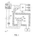
- FIG. 1depicts a schematic illustration of a wafer processing system 10 that can be used to form one or more tantalum-nitride barrier layers in accordance with aspects of the present invention described herein.
- System 10comprises process chamber 100 , gas panel 130 , control unit 110 , along with other hardware components such as power supply 106 and vacuum pump 102 .
- process chamber 100For purposes of clarity, salient features of process chamber 100 are briefly described below.
- Process chamber 100generally houses a support pedestal 150 , which is used to support a substrate such as a semiconductor wafer 190 within process chamber 100 .
- semiconductor wafer 190can be heated to some desired temperature or within some desired temperature range prior to layer formation using heater 170 .
- wafer support pedestal 150is heated by an embedded heating element 170 .
- pedestal 150may be resistively heated by applying an electric current from an AC power supply 106 to heating element 170 .
- Wafer 190is, in turn, heated by pedestal 150 , and may be maintained within a desired process temperature range of, for example, about 20 degrees Celsius to about 500 degrees Celsius.
- Temperature sensor 172such as a thermocouple, may be embedded in wafer support pedestal 150 to monitor the pedestal temperature of 150 in a conventional manner. For example, measured temperature may be used in a feedback loop to control electric current applied to heating element 170 from power supply 106 , such that wafer temperature can be maintained or controlled at a desired temperature or within a desired temperature range suitable for a process application. Pedestal 150 may optionally be heated using radiant heat (not shown).
- Vacuum pump 102is used to evacuate process gases from process chamber 100 and to help maintain a desired pressure or desired pressure within a pressure range inside chamber 100 .
- Orifice 120 through a wall of chamber 100is used to introduce process gases into process chamber 100 . Sizing of orifice 120 conventionally depends on the size of process chamber 100 .
- Orifice 120is coupled to gas panel 130 in part by valve 125 .
- Gas panel 130is configured to receive and then provide a resultant process gas from two or more gas sources 135 , 136 to process chamber 100 through orifice 120 and valve 125 .
- Gas sources 135 , 136may store precursors in a liquid phase at room temperature, which are later heated when in gas panel 130 to convert them to a vapor-gas phase for introduction into chamber 100 .
- Gas panel 130is further configured to receive and then provide a purge gas from purge gas source 138 to process chamber 100 through orifice 120 and valve 125 .
- Control unit 110such as a programmed personal computer, work station computer, and the like, is configured to control flow of various process gases through gas panel 130 as well as valve 125 during different stages of a wafer process sequence.
- control unit 110comprises central processing unit (CPU) 112 , support circuitry 114 , and memory 116 containing associated control software 113 .
- control unit 110may be configured to be responsible for automated control of other activities used in wafer processing—such as wafer transport, temperature control, chamber evacuation, among other activities, some of which are described elsewhere herein.
- Control unit 110may be one of any form of general purpose computer processor that can be used in an industrial setting for controlling various chambers and sub-processors.
- CPU 112may use any suitable memory 116 , such as random access memory, read only memory, floppy disk drive, hard disk, or any other form of digital storage, local or remote.
- Various support circuitsmay be coupled to CPU 112 for supporting system 10 .
- Software routines 113 as requiredmay be stored in memory 116 or executed by a second computer processor that is remotely located (not shown). Bi-directional communications between control unit 110 and various other components of wafer processing system 10 are handled through numerous signal cables collectively referred to as signal buses 118 , some of which are illustrated in FIG. 1 .
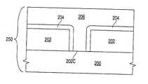
- FIGS. 2 a - 2 cillustrate exemplary embodiment portions of tantalum-nitride layer formation for integrated circuit fabrication of an interconnect structure in accordance with one or more aspects of the present invention.
- substrate 200refers to any workpiece upon which film processing is performed, and substrate structure 250 is used to denote substrate 200 as well as other material layers formed on substrate 200 .
- substrate 200may be a silicon semiconductor wafer, or other material layer, which has been formed on wafer 190 (shown in FIG. 1 ).
- FIG. 2 ashows a cross-sectional view of a substrate structure 250 , having a dielectric layer 202 thereon.
- Dielectric layer 202may be an oxide, a silicon oxide, carbon-silicon-oxide, a fluoro-silicon, a porous dielectric, or other suitable dielectric formed and patterned to provide contact hole or via 202 H extending to an exposed surface portion 202 T of substrate 200 . More particularly, it will be understood by those with skill in the art that the present invention may be used in a dual damascene process flow.
- FIG. 2 billustratively shows tantalum-nitride layer 204 formed on substrate structure 250 .
- Tantalum-nitride layer 204is formed by chemisorbing monolayers of a tantalum containing compound and a nitrogen containing compound on substrate structure 250 .
- a portion of layer 204may be removed by etching in a well-known manner to expose a portion 202 C of substrate 200 .
- Portion 202 Cmay be part of a transistor gate stack, a capacitor plate, a node, a conductor, or like conductive element.
- contact layer 206may be formed thereon, for example, to form an interconnect structure.
- Contact layer 206may be selected from a group of aluminum (Al), copper (Cu), tungsten (W), and combinations thereof.
- Contact layer 206may be formed, for example, using chemical vapor deposition (CVD), physical vapor deposition (PVD), electroplating, or a combination thereof.
- CVDchemical vapor deposition
- PVDphysical vapor deposition
- electroplatingor a combination thereof.
- an aluminum (Al) layermay be deposited from a reaction of a gas mixture containing dimethyl aluminum hydride (DMAH) and hydrogen (H 2 ) or argon (Ar) or other DMAH containing mixtures
- a CVD copper layermay be deposited from a gas mixture containing Cu(hfac) 2 (copper (II) hexafluoro acetylacetonate), Cu(fod) 2 (copper (II) heptafluoro dimethyl octanediene), Cu(hfac) TMVS (copper (I) hexafluoro acetylacetonate trimethylvinylsilane) or combinations thereof,
- layer 206may be a refractory metal compound including but not limited to titanium (Ti), tungsten (W), tantalum (Ta), zirconium (Zr), hafnium (Hf), molybdenum (Mo), niobium (Nb), vanadium (V), and chromium (Cr), among others.
- a refractory metalis combined with reactive species, such as for example chlorine (Cl) or fluorine (F), and is provided with another gas to form a refractory metal compound.
- TiCl 4titanium tetrachloride
- WF 6tantalum pentachloride
- ZrCl 4zirconium tetrachloride
- HfCl 4hafnium tetrachloride
- MoCl 5molybdenum pentachloride
- layer 206is shown as formed on layer 204 , it should be understood that layer 204 may be used in combination with one or more other barrier layers formed by CVD or PVD. Accordingly, layer 204 need not be in direct contact with layer 206 , but an intervening layer may exist between layer 206 and layer 204 .
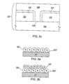
- Monolayersare chemisorbed by sequentially providing a tantalum containing compound and a nitrogen containing compound to a process chamber. Monolayers of a tantalum containing compound and a nitrogen containing compound are alternately chemisorbed on a substrate 300 as illustratively shown in FIGS. 3 a - 3 c.
- FIG. 3 adepicts a cross-sectional view of an exemplary portion of substrate 300 in a stage of integrated circuit fabrication, and more particularly at a stage of barrier layer formation.
- Tantalum layer 305is formed by chemisorbing a tantalum-containing compound on surface portion 300 T of substrate 300 by introducing a pulse of a tantalum containing gas 135 (shown in FIG. 1 ) into process chamber 100 (shown in FIG. 1 ).
- Tantalum containing gas 135(shown in FIG. 1 ) may be a tantalum based organometallic precursor or a derivative thereof.
- Such precursorsinclude but are not limited to pentakis(ethylmethylamino) tantalum (PEMAT; Ta(N(Et)Me) 5 ), pentakis(diethylamino) tantalum (PDEAT; Ta(NEt 2 ) 5 ), pentakis(dimethylamino) tantalum (PDMAT; Ta(NMe 2 ) 5 ) or a derivative thereof.
- Other tantalum containing precursorsinclude TBTDET ( t BuNTa(NEt 2 ) 3 or C 16 H 39 N 4 Ta), tantalum halides (e.g., TaX 5 , where X is F, B or C) or a derivative thereof.
- Wafer 190is maintained approximately below a thermal decomposition temperature of a selected tantalum precursor or a derivative thereof to be used and maintained at a pressure of approximately less than 100 Torr. Additionally, wafer 190 may be heated by heating element 170 .
- An exemplary temperature range for precursors identified hereinis approximately 20 to 400 degrees Celsius. For example, approximately 150 to 300 degrees Celsius may be used for PEMAT.
- temperatures below a thermal decomposition temperaturemay be used, it should be understood that other temperatures, namely those above a thermal decomposition temperature, may be used.
- An example temperature ranges above a thermal decomposition temperatureis approximately 400 to 600 degrees Celsius. Accordingly, some thermal decomposition may occur; however, the main, more than 50 percent, deposition activity is by chemisorption. More generally, wafer surface temperature needs to be high enough to induce significant chemisorption of precursors instead of physisorption, but low enough to prevent significant decomposition of precursors.
- the primary growth modewill be ALD. Accordingly, such a film will tend to have ALD properties.
- this tantalum-containing precursorcombines tantalum atoms with one or more reactive species.
- these reactive speciesform byproducts that are transported from process chamber 100 by vacuum system 102 while leaving tantalum deposited on surface portion 300 T.
- a precursormay be in an intermediate state when on a surface of wafer 190 .
- each layermay contain more than simply elements of tantalum (Ta) or nitrogen (N); rather, the existence of more complex molecules having carbon (C), hydrogen (H), and/or oxygen ( 0 ) is probable.
- a surfacemay saturate after exposure to a precursor forming a layer having more or less than a monolayer of either tantalum (Ta) or nitrogen (N).
- Tatantalum
- Nnitrogen
- This composition or structurewill depend on available free energy on a surface of wafer 190 , as well as atoms or molecules involved. Once all available sites are occupied by tantalum atoms, further chemisorption of tantalum is blocked, and thus the reaction is self-limiting.
- a tantalum containing compoundis chemisorbed onto substrate 300 .
- excess tantalum containing compoundis removed from process chamber 10 by vacuum system 102 (shown in FIG. 1 ). Additionally, a pulse of purge gas 138 (shown in FIG. 1 ) may be supplied to process chamber 10 to facilitate removal of excess tantalum containing compound.
- suitable purge gasesinclude but are not limited to helium (He), nitrogen (N 2 ), argon (Ar), and hydrogen (H 2 ), among others, and combinations thereof that may be used.
- a pulse of ammonia gas (NH 3 ) 136is introduced into process chamber 100 .
- Process chamber 100 and wafer 190may be maintained at approximately the same temperature and pressure range as used for formation of layer 305 .
- a layer 307 of nitrogenis illustratively shown as chemisorbed on tantalum layer 305 at least in part in response to introduction of ammonia gas 136 . While not wishing to be bound by theory, it is believed that nitrogen layer 307 is formed in a similar self-limiting manner as was tantalum layer 305 .
- Each tantalum layer 305 and nitrogen layer 307 in any combination and in direct contact with one anotherform a sublayer 309 , whether or not either or both or neither is a monolayer.
- N containing precursors gasesmay be used including but not limited to N x H y for x and y integers (e.g., N 2 H 4 ), N 2 plasma source, NH 2 N(CH 3 ) 2 , among others.
- Tantalum-nitride layer 204may, for example, have a thickness in a range of approximately 0.0002 microns (2 Angstrom) to about 0.05 microns (500 Angstrom), though a thickness of approximately 0.001 microns (10 Angstrom) to about 0.005 microns (50 Angstrom) may be a sufficient barrier.
- a tantalum-nitride layer 204may be used as a thin film insulator or dielectric, or may be used as a protective layer for example to prevent corrosion owing to layer 204 being relatively inert or non-reactive.
- layer 204may be used to coat any of a variety of geometries.
- tantalum-nitride layer 204 formationis depicted as starting with chemisorption of a tantalum containing compound on substrate 300 followed by chemisorption of a nitrogen containing compound.
- chemisorptionmay begin with a layer of a nitrogen containing compound on substrate 300 followed by a layer of a tantalum containing compound.
- Pulse time for each pulse of a tantalum containing compound, a nitrogen containing compound, and a purge gasis variable and depends on volume capacity of a deposition chamber 100 employed as well as vacuum system 102 coupled thereto. Similarly, time between each pulse is also variable and depends on volume capacity of process chamber 100 as well as vacuum system 102 coupled thereto. However, in general, wafer 190 surface must be saturated by the end of a pulse time, where pulse time is defined as time a surface is exposed to a precursor.
- precursor gasesshould not mix at or near the wafer surface to prevent co-reaction (a co-reactive embodiment is disclosed elsewhere herein), and thus at least one gas purge or pump evacuation between precursor pulses should be used to prevent mixing.
- a pulse time of less than about 1 second for a tantalum containing compound and a pulse time of less than about 1 second for a nitrogen containing compoundis typically sufficient to chemisorb alternating monolayers that comprise tantalum-nitride layer 204 on substrate 300 .
- a pulse time of less than about 1 second for purge gas 138is typically sufficient to remove reaction byproducts as well as any residual materials remaining in process chamber 100 .
- Sequential deposition as describedadvantageously provides good step coverage and conformality, due to using a chemisorption mechanism for forming tantalum-nitride layer 204 .
- each of uniformity and step coverageis approximately 100 percent.
- precision controlled thickness of tantalum-nitride layer 204may be achieved down to a single layer of atoms.
- deposition areais largely independent of the amount of precursor gas remaining in a reaction chamber once a layer has been formed.
- cycleit is meant a sequence of pulse gases, including precursor and purge gases, and optionally one or more pump evacuations. Also, by using ALD, gas-phase reactions between precursors are minimized to reduce generation of unwanted particles.
- pulses of gases 135 and 136are both applied to chamber 100 at the same time.
- gases 135 and 136namely, tantalum and nitrogen containing compounds
- An exampleis PEMAT and NH 3 , though other tantalum-organic and nitrogen precursors may be used. Step coverage and conformality is good at approximately 95 to 100 percent for each.
- deposition rateis approximately 0.001 to 0.1 microns per second. Because a co-reaction is used, purging between sequential pulses of alternating precursors is avoided, as is done in ALD.
- Wafer surface temperatureis maintained high enough to sustain reaction between two precursors. This temperature may be below chemisorption temperature of one or both precursors. Accordingly, temperature should be high enough for sufficient diffusion of molecules or atoms.
- Wafer surface temperatureis maintained low enough to avoid significant decomposition of precursors. However, more decomposition of precursors may be acceptable for co-reaction than for sequentially reacting precursors in an ALD process.
- wafer 190 surface diffusion rate of molecules or atomsshould be greater than precursors' reaction rate which should be greater precursors' decomposition rate.
- substrate structure 250may be plasma annealed.
- FIG. 4there is illustratively shown a schematic diagram of an exemplary portion of a process system 10 P in accordance with an aspect of the present invention.
- Process system 10 Pis similar to process system 10 , except for additions of one or more RF power supplies 410 and 412 , showerhead 400 , gas source 405 , and matching network(s) 411 .
- a separate plasma process systemmay be used; however, by using a CVD/PVD process system 10 P, less handling of substrate structure 250 is involved, as layer 204 may be formed and annealed in a same chamber 100 .
- showerhead 400 and wafer support pedestal 150provide in part spaced apart electrodes. An electric field may be generated between these electrodes to ignite a process gas introduced into chamber 100 to provide a plasma 415 .
- argonis introduced into chamber 100 from gas source 405 to provide an argon plasma.
- gas source 405may be omitted for gas source 138 .
- pedestal 150is coupled to a source of radio frequency (RF) power source 412 through a matching network 411 , which in turn may be coupled to control unit 110 .
- RF power source 410may be coupled to showerhead 400 and matching network 411 , which in turn may be coupled to control unit 110 .
- matching network 411may comprise different circuits for RF power sources 410 and 412 , and both RF power sources 410 and 412 may be coupled to showerhead 400 and pedestal 150 , respectively.
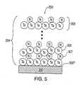
- substrate structure 250 having one or more iterations or tantalum-nitride sublayers 309is located in process chamber 401 .
- Argon (Ar) gas from gas source 405is introduced into chamber 401 to plasma anneal substrate structure 250 .
- plasma annealingreduces nitrogen content of one or more sublayers 309 by sputtering off nitrogen, which in turn reduces resistivity.
- plasma annealingis believed to make tantalum-nitride layer 204 more tantalum-rich as compared to a non-plasma annealed tantalum-nitride layer 204 .
- a 1:1 Ta:N filmmay be annealed to a 2:1 Ta:N film.
- Tantalum-nitride films having a sheet resistance of approximately equal to or less than 1200 microohms-cm for 0.004 micron (40 Angstrom) filmsmay be achieved.
- non-chemically reactive gaseswith respect to layer 204 may be used for physically displacing nitrogen from layer 204 , including but not limited to neon (Ne), xenon (Xe), helium (He), and hydrogen (H 2 ).
- Neneon
- Xexenon
- Hehelium
- H 2hydrogen
- a plasma-gas that does not chemically react with a tantalum-nitride filmit is desirable to have a plasma-gas atom or molecule with an atomic-mass closer to N than to Ta in order to have preferential sputtering of the N.
- a chemically reactive processmay be used where a gas is selected which preferentially reacts for removal of N while leaving Ta.
- Plasma annealingmay be done after formation of each nitrogen layer 307 , or may be done after formation of a plurality of layers 307 . With respect to the latter, plasma annealing may take place after approximately every 0.003 to 0.005 microns (30 to 50 Angstroms) of layer 204 or after formation of approximately every 7 to 10 sublayers 309 . However, plasma annealing may be done after formation of a sublayer 309 , which is approximately 0.0001 to 0.0004 microns (1 to 4 Angstroms).
- Plasma annealing with argonmay be done with a wafer temperature in a range of approximately 20 to 450 degrees Celsius and a chamber pressure of approximately 0.1 to 50 Torr with a flow rate of argon in a range of approximately 10 to 2,000 standard cubic centimeters per minute (sccm) with a plasma treatment time approximately equal to or greater than one second.
- a tantalum-nitride filmshould be annealed at a temperature, which does not melt, sublime, or decompose such a tantalum-nitride film.
Landscapes
- Chemical & Material Sciences (AREA)
- Engineering & Computer Science (AREA)
- Physics & Mathematics (AREA)
- Chemical Kinetics & Catalysis (AREA)
- General Chemical & Material Sciences (AREA)
- General Physics & Mathematics (AREA)
- Metallurgy (AREA)
- Computer Hardware Design (AREA)
- Microelectronics & Electronic Packaging (AREA)
- Power Engineering (AREA)
- Condensed Matter Physics & Semiconductors (AREA)
- Organic Chemistry (AREA)
- Materials Engineering (AREA)
- Mechanical Engineering (AREA)
- Manufacturing & Machinery (AREA)
- Plasma & Fusion (AREA)
- Crystallography & Structural Chemistry (AREA)
- Inorganic Chemistry (AREA)
- Electromagnetism (AREA)
- Chemical Vapour Deposition (AREA)
- Internal Circuitry In Semiconductor Integrated Circuit Devices (AREA)
- Electrodes Of Semiconductors (AREA)
Abstract
Description
- This application is a continuation of U.S. Ser. No. 11/240,189, filed Sep. 30, 2005, which is a continuation of U.S. Ser. No. 11/088,072, filed Mar. 23, 2005, now U.S. Pat. No. 7,094,680, which is a continuation of co-pending U.S. Ser. No. 09/776,329, filed Feb. 2, 2001, now U.S. Pat. No. 6,951,804, all of which are hereby incorporated by reference in their entireties.
- 1. Field of the Invention
- The present invention relates to formation of one or more barrier layers and, more particularly, to one or more barrier layers formed using chemisorption techniques.
- 2. Description of the Related Art
- In manufacturing integrated circuits, one or more barrier layers are often used to inhibit diffusion of one or more materials in metal layers, as well as other impurities from intermediate dielectric layers, into elements underlying such barrier layers, such as transistor gates, capacitor dielectrics, transistor wells, transistor channels, electrical barrier regions, interconnects, among other known elements of integrated circuits.
- Though a barrier layer may limit to prevent migration of unwanted materials into such elements, its introduction creates an interface at least in part between itself and one or more metal layers. For sub half-micron (0.5 μm) semiconductor devices, microscopic reaction at an interface between metal and barrier layers can cause degradation of integrated circuits, including but not limited to increased electrical resistance of such metal layers. Accordingly, though barrier layers have become a component for improving reliability of interconnect metallization schemes, it is desirable to mitigate “side effects” caused by introduction of such barrier layers.
- Compounds of refractory metals such as, for example, nitrides, borides, and carbides are targets as diffusion barriers because of their chemical inertness and low resistivities (e.g., sheet resistivities typically less than about 200 μΩ-cm). In particular, borides such as, including but not limited to titanium diboride (TiB2), have been used as a barrier material owing to their low sheet resistivities (e.g., resistivities less than about 150 μΩ-cm).
- Boride barrier layers are conventionally formed using chemical vapor deposition (CVD) techniques. For example, titanium tetrachloride (TiCl4) may be reacted with diborane (B2H6) to form titanium diboride (TiB2) using CVD. However, when Cl-based chemistries are used to form boride barrier layers, reliability problems can occur. In particular, boride layers formed using CVD chlorine-based chemistries typically have a relatively high chlorine (Cl) content, namely, chlorine content greater than about 3 percent. A high chlorine content is undesirable because migrating chlorine from a boride barrier layer into adjacent interconnection layer may increase contact resistance of such interconnection layer and potentially change one or more characteristics of integrated circuits made therewith.
- Therefore, a need exists for barrier layers for integrated circuit fabrication with little to no side effects owing to their introduction. Particularly desirable would be a barrier layer useful for interconnect structures.
- An aspect of the present invention is film deposition for integrated circuit fabrication. More particularly, at least one element from a first precursor and at least one element from a second precursor is chemisorbed on a surface. The at least one element from the first precursor and the at least one element from the second precursor are chemisorbed to provide a tantalum-nitride film. This sequence may be repeated to increase tantalum-nitride layer thickness. This type of deposition process is sometimes called atomic layer deposition (ALD). Such a tantalum-nitride layer may be used as a barrier layer.
- Another aspect is forming the tantalum-nitride layer using in part annealing of at least one tantalum-nitride sublayer. This annealing may be done with a plasma.
- Another aspect is using a plasma source gas as a nitrogen precursor. The plasma source gas may be used to provide a plasma, which may be sequentially reacted or co-reacted with a tantalum containing precursor.
- In another aspect, a method of film deposition for integrated circuit fabrication includes forming a tantalum nitride layer by sequentially chemisorbing a tantalum precursor and a nitrogen precursor on a substrate disposed in a process chamber. A nitrogen concentration of the tantalum nitride layer is reduced by exposing the substrate to a plasma annealing process. A metal-containing layer is subsequently deposited on the tantalum nitride layer.
- In another aspect, a method of film deposition for integrated circuit fabrication includes forming a tantalum nitride layer with a first nitrogen concentration on a substrate by an atomic layer deposition process. An upper portion of the tantalum nitride layer is exposed to a plasma annealing process to form a tantalum-containing layer with a second nitrogen concentration. A metal-containing layer is then deposited on the tantalum-containing layer.
- In another aspect, a method of film deposition for integrated circuit fabrication includes forming a tantalum-containing layer with a sheet resistance of about 1,200 μΩ-cm or less by a plasma annealing process on a tantalum nitride layer deposited by an atomic layer deposition process on a substrate.
- In yet another aspect, a method of forming a material on a substrate is disclosed. In one embodiment, the method includes forming a tantalum nitride layer on a substrate disposed in a plasma process chamber by sequentially exposing the substrate to a tantalum precursor and a nitrogen precursor, followed by reducing a nitrogen concentration of the tantalum nitride layer by exposing the substrate to a plasma annealing process. A metal-containing layer is then deposited on the tantalum nitride layer by a deposition process.
- These and other aspects of the present invention will be more apparent from the following description.
- So that the manner in which the above recited features of the present invention can be understood in detail, a more particular description of the invention, briefly summarized above, may be had by reference to embodiments, some of which are illustrated in the appended drawings. It is to be noted, however, that the appended drawings illustrate only typical embodiments of this invention and are therefore not to be considered limiting of its scope, for the invention may admit to other equally effective embodiments.
FIGS. 1 and 4 depict schematic illustrations of exemplary portions of process systems in accordance with one or more integrated circuit fabrication aspects of the present invention;FIGS. 2 a-2cdepict cross-sectional views of a substrate structure at different stages of integrated circuit fabrication;FIGS. 3 a-3cdepict cross-sectional views of a substrate at different stages of chemisorption to form a barrier layer; andFIG. 5 depicts a cross-sectional view of a substrate structure at different stages of integrated circuit fabrication incorporating one or more tantalum-nitride barrier sublayers post plasma anneal.FIG. 1 depicts a schematic illustration of awafer processing system 10 that can be used to form one or more tantalum-nitride barrier layers in accordance with aspects of the present invention described herein.System 10 comprisesprocess chamber 100,gas panel 130,control unit 110, along with other hardware components such aspower supply 106 andvacuum pump 102. For purposes of clarity, salient features ofprocess chamber 100 are briefly described below.Process chamber 100 generally houses asupport pedestal 150, which is used to support a substrate such as a semiconductor wafer190 withinprocess chamber 100. Depending on process requirements,semiconductor wafer 190 can be heated to some desired temperature or within some desired temperature range prior to layerformation using heater 170.- In
chamber 100,wafer support pedestal 150 is heated by an embeddedheating element 170. For example,pedestal 150 may be resistively heated by applying an electric current from anAC power supply 106 toheating element 170. Wafer190 is, in turn, heated bypedestal 150, and may be maintained within a desired process temperature range of, for example, about 20 degrees Celsius to about 500 degrees Celsius. Temperature sensor 172, such as a thermocouple, may be embedded inwafer support pedestal 150 to monitor the pedestal temperature of150 in a conventional manner. For example, measured temperature may be used in a feedback loop to control electric current applied toheating element 170 frompower supply 106, such that wafer temperature can be maintained or controlled at a desired temperature or within a desired temperature range suitable for a process application.Pedestal 150 may optionally be heated using radiant heat (not shown).Vacuum pump 102 is used to evacuate process gases fromprocess chamber 100 and to help maintain a desired pressure or desired pressure within a pressure range insidechamber 100.Orifice 120 through a wall ofchamber 100 is used to introduce process gases intoprocess chamber 100. Sizing oforifice 120 conventionally depends on the size ofprocess chamber 100.Orifice 120 is coupled togas panel 130 in part byvalve 125.Gas panel 130 is configured to receive and then provide a resultant process gas from two ormore gas sources chamber 100 throughorifice 120 andvalve 125.Gas sources gas panel 130 to convert them to a vapor-gas phase for introduction intochamber 100.Gas panel 130 is further configured to receive and then provide a purge gas frompurge gas source 138 to processchamber 100 throughorifice 120 andvalve 125.Control unit 110, such as a programmed personal computer, work station computer, and the like, is configured to control flow of various process gases throughgas panel 130 as well asvalve 125 during different stages of a wafer process sequence. Illustratively,control unit 110 comprises central processing unit (CPU)112,support circuitry 114, andmemory 116 containing associatedcontrol software 113. In addition to control of process gases throughgas panel 130,control unit 110 may be configured to be responsible for automated control of other activities used in wafer processing—such as wafer transport, temperature control, chamber evacuation, among other activities, some of which are described elsewhere herein.Control unit 110 may be one of any form of general purpose computer processor that can be used in an industrial setting for controlling various chambers and sub-processors.CPU 112 may use anysuitable memory 116, such as random access memory, read only memory, floppy disk drive, hard disk, or any other form of digital storage, local or remote. Various support circuits may be coupled toCPU 112 for supportingsystem 10.Software routines 113 as required may be stored inmemory 116 or executed by a second computer processor that is remotely located (not shown). Bi-directional communications betweencontrol unit 110 and various other components ofwafer processing system 10 are handled through numerous signal cables collectively referred to assignal buses 118, some of which are illustrated inFIG. 1 .FIGS. 2 a-2cillustrate exemplary embodiment portions of tantalum-nitride layer formation for integrated circuit fabrication of an interconnect structure in accordance with one or more aspects of the present invention. For purposes of clarity,substrate 200 refers to any workpiece upon which film processing is performed, andsubstrate structure 250 is used to denotesubstrate 200 as well as other material layers formed onsubstrate 200. Depending on processing stage,substrate 200 may be a silicon semiconductor wafer, or other material layer, which has been formed on wafer190 (shown inFIG. 1 ).FIG. 2 a, for example, shows a cross-sectional view of asubstrate structure 250, having adielectric layer 202 thereon.Dielectric layer 202 may be an oxide, a silicon oxide, carbon-silicon-oxide, a fluoro-silicon, a porous dielectric, or other suitable dielectric formed and patterned to provide contact hole or via202H extending to an exposedsurface portion 202T ofsubstrate 200. More particularly, it will be understood by those with skill in the art that the present invention may be used in a dual damascene process flow.FIG. 2 billustratively shows tantalum-nitride layer 204 formed onsubstrate structure 250. Tantalum-nitride layer 204 is formed by chemisorbing monolayers of a tantalum containing compound and a nitrogen containing compound onsubstrate structure 250.- Referring to
FIG. 2 c, after the formation of tantalum-nitride layer 204, a portion oflayer 204 may be removed by etching in a well-known manner to expose aportion 202C ofsubstrate 200.Portion 202C may be part of a transistor gate stack, a capacitor plate, a node, a conductor, or like conductive element. Next,contact layer 206 may be formed thereon, for example, to form an interconnect structure.Contact layer 206 may be selected from a group of aluminum (Al), copper (Cu), tungsten (W), and combinations thereof. Contact layer 206 may be formed, for example, using chemical vapor deposition (CVD), physical vapor deposition (PVD), electroplating, or a combination thereof. For example, an aluminum (Al) layer may be deposited from a reaction of a gas mixture containing dimethyl aluminum hydride (DMAH) and hydrogen (H2) or argon (Ar) or other DMAH containing mixtures, a CVD copper layer may be deposited from a gas mixture containing Cu(hfac)2(copper (II) hexafluoro acetylacetonate), Cu(fod)2(copper (II) heptafluoro dimethyl octanediene), Cu(hfac) TMVS (copper (I) hexafluoro acetylacetonate trimethylvinylsilane) or combinations thereof, and a CVD tungsten layer may be deposited from a gas mixture containing tungsten hexafluoride (WF6). A PVD layer is deposited from a copper target, an aluminum target, or a tungsten target.- Moreover,
layer 206 may be a refractory metal compound including but not limited to titanium (Ti), tungsten (W), tantalum (Ta), zirconium (Zr), hafnium (Hf), molybdenum (Mo), niobium (Nb), vanadium (V), and chromium (Cr), among others. Conventionally, a refractory metal is combined with reactive species, such as for example chlorine (Cl) or fluorine (F), and is provided with another gas to form a refractory metal compound. For example, titanium tetrachloride (TiCl4), tungsten hexafluoride (WF6), tantalum pentachloride (TaCl5), zirconium tetrachloride (ZrCl4), hafnium tetrachloride (HfCl4), molybdenum pentachloride (MoCl5), niobium pentachloride (NbCl5), vanadium pentachloride (VCl5), or chromium tetrachloride (CrCl4) may be used as a refractory metal-containing compound gas. - Though
layer 206 is shown as formed onlayer 204, it should be understood thatlayer 204 may be used in combination with one or more other barrier layers formed by CVD or PVD. Accordingly,layer 204 need not be in direct contact withlayer 206, but an intervening layer may exist betweenlayer 206 andlayer 204. - Monolayers are chemisorbed by sequentially providing a tantalum containing compound and a nitrogen containing compound to a process chamber. Monolayers of a tantalum containing compound and a nitrogen containing compound are alternately chemisorbed on a
substrate 300 as illustratively shown inFIGS. 3 a-3c. FIG. 3 adepicts a cross-sectional view of an exemplary portion ofsubstrate 300 in a stage of integrated circuit fabrication, and more particularly at a stage of barrier layer formation.Tantalum layer 305 is formed by chemisorbing a tantalum-containing compound onsurface portion 300T ofsubstrate 300 by introducing a pulse of a tantalum containing gas135 (shown inFIG. 1 ) into process chamber100 (shown inFIG. 1 ). Tantalum containing gas135 (shown inFIG. 1 ) may be a tantalum based organometallic precursor or a derivative thereof. Examples of such precursors include but are not limited to pentakis(ethylmethylamino) tantalum (PEMAT; Ta(N(Et)Me)5), pentakis(diethylamino) tantalum (PDEAT; Ta(NEt2)5), pentakis(dimethylamino) tantalum (PDMAT; Ta(NMe2)5) or a derivative thereof. Other tantalum containing precursors include TBTDET (tBuNTa(NEt2)3or C16H39N4Ta), tantalum halides (e.g., TaX5, where X is F, B or C) or a derivative thereof.Wafer 190 is maintained approximately below a thermal decomposition temperature of a selected tantalum precursor or a derivative thereof to be used and maintained at a pressure of approximately less than 100 Torr. Additionally,wafer 190 may be heated byheating element 170. An exemplary temperature range for precursors identified herein is approximately 20 to 400 degrees Celsius. For example, approximately 150 to 300 degrees Celsius may be used for PEMAT.- Though temperatures below a thermal decomposition temperature may be used, it should be understood that other temperatures, namely those above a thermal decomposition temperature, may be used. An example temperature ranges above a thermal decomposition temperature is approximately 400 to 600 degrees Celsius. Accordingly, some thermal decomposition may occur; however, the main, more than 50 percent, deposition activity is by chemisorption. More generally, wafer surface temperature needs to be high enough to induce significant chemisorption of precursors instead of physisorption, but low enough to prevent significant decomposition of precursors. If the amount of decomposition during each precursor deposition is significantly less than a layer, then the primary growth mode will be ALD. Accordingly, such a film will tend to have ALD properties. However, it is possible if a precursor significantly decomposes, but an intermediate reactant is obtained preventing further precursor decomposition after a layer of intermediate reactant is deposited, then an ALD growth mode may still be obtained.
- While not wishing to be bound by theory, it is believed that this tantalum-containing precursor combines tantalum atoms with one or more reactive species. During
tantalum layer 305 formation, these reactive species form byproducts that are transported fromprocess chamber 100 byvacuum system 102 while leaving tantalum deposited onsurface portion 300T. However, composition and structure of precursors on a surface during atomic-layer deposition (ALD) is not precisely known. A precursor may be in an intermediate state when on a surface ofwafer 190. For example, each layer may contain more than simply elements of tantalum (Ta) or nitrogen (N); rather, the existence of more complex molecules having carbon (C), hydrogen (H), and/or oxygen (0) is probable. Additionally, a surface may saturate after exposure to a precursor forming a layer having more or less than a monolayer of either tantalum (Ta) or nitrogen (N). This composition or structure will depend on available free energy on a surface ofwafer 190, as well as atoms or molecules involved. Once all available sites are occupied by tantalum atoms, further chemisorption of tantalum is blocked, and thus the reaction is self-limiting. - After
layer 305 of a tantalum containing compound is chemisorbed ontosubstrate 300, excess tantalum containing compound is removed fromprocess chamber 10 by vacuum system102 (shown inFIG. 1 ). Additionally, a pulse of purge gas138 (shown inFIG. 1 ) may be supplied to processchamber 10 to facilitate removal of excess tantalum containing compound. Examples of suitable purge gases include but are not limited to helium (He), nitrogen (N2), argon (Ar), and hydrogen (H2), among others, and combinations thereof that may be used. - With continuing reference to
FIGS. 3 a-cand renewed reference toFIG. 1 , afterprocess chamber 100 has been purged, a pulse of ammonia gas (NH3)136 is introduced intoprocess chamber 100.Process chamber 100 andwafer 190 may be maintained at approximately the same temperature and pressure range as used for formation oflayer 305. - In
FIG. 3 b, alayer 307 of nitrogen is illustratively shown as chemisorbed ontantalum layer 305 at least in part in response to introduction ofammonia gas 136. While not wishing to be bound by theory, it is believed thatnitrogen layer 307 is formed in a similar self-limiting manner as wastantalum layer 305. Eachtantalum layer 305 andnitrogen layer 307 in any combination and in direct contact with one another form asublayer 309, whether or not either or both or neither is a monolayer. Though ammonia gas is used, other N containing precursors gases may be used including but not limited to NxHyfor x and y integers (e.g., N2H4), N2plasma source, NH2N(CH3)2, among others. - After an ammonia gas compound is chemisorbed onto
tantalum layer 305 onsubstrate 300 to formnitrogen monolayer 307, excess ammonia gas compound is removed fromprocess chamber 10 byvacuum system 102, and additionally, a pulse ofpurge gas 138 may be supplied to processchamber 10 to facilitate this removal. - Thereafter, as shown in
FIG. 3 c, tantalum and nitrogen layer deposition in an alternating sequence may be repeated with interspersed purges until a desiredlayer 204 thickness is achieved. Tantalum-nitride layer 204 may, for example, have a thickness in a range of approximately 0.0002 microns (2 Angstrom) to about 0.05 microns (500 Angstrom), though a thickness of approximately 0.001 microns (10 Angstrom) to about 0.005 microns (50 Angstrom) may be a sufficient barrier. Moreover, a tantalum-nitride layer 204 may be used as a thin film insulator or dielectric, or may be used as a protective layer for example to prevent corrosion owing tolayer 204 being relatively inert or non-reactive. Advantageously,layer 204 may be used to coat any of a variety of geometries. - In
FIGS. 3 a-3c,tantalum-nitride layer 204 formation is depicted as starting with chemisorption of a tantalum containing compound onsubstrate 300 followed by chemisorption of a nitrogen containing compound. Alternatively, chemisorption may begin with a layer of a nitrogen containing compound onsubstrate 300 followed by a layer of a tantalum containing compound. - Pulse time for each pulse of a tantalum containing compound, a nitrogen containing compound, and a purge gas is variable and depends on volume capacity of a
deposition chamber 100 employed as well asvacuum system 102 coupled thereto. Similarly, time between each pulse is also variable and depends on volume capacity ofprocess chamber 100 as well asvacuum system 102 coupled thereto. However, in general,wafer 190 surface must be saturated by the end of a pulse time, where pulse time is defined as time a surface is exposed to a precursor. There is some variability here, for example (1) a lower chamber pressure of a precursor will require a longer pulse time; (2) a lower precursor gas flow rate will require a longer time for chamber pressure to rise and stabilize requiring a longer pulse time; and (3) a large-volume chamber will take longer to fill, longer for chamber pressure to stabilize thus requiring a longer pulse time. In general, precursor gases should not mix at or near the wafer surface to prevent co-reaction (a co-reactive embodiment is disclosed elsewhere herein), and thus at least one gas purge or pump evacuation between precursor pulses should be used to prevent mixing. - Generally, a pulse time of less than about 1 second for a tantalum containing compound and a pulse time of less than about 1 second for a nitrogen containing compound is typically sufficient to chemisorb alternating monolayers that comprise tantalum-
nitride layer 204 onsubstrate 300. A pulse time of less than about 1 second forpurge gas 138 is typically sufficient to remove reaction byproducts as well as any residual materials remaining inprocess chamber 100. - Sequential deposition as described advantageously provides good step coverage and conformality, due to using a chemisorption mechanism for forming tantalum-
nitride layer 204. With complete or near complete saturation after each exposure ofwafer 190 to a precursor, each of uniformity and step coverage is approximately 100 percent. Because atomic layer deposition is used, precision controlled thickness of tantalum-nitride layer 204 may be achieved down to a single layer of atoms. Furthermore, in ALD processes, since it is believed that only about one atomic layer may be absorbed on a topographic surface per “cycle,” deposition area is largely independent of the amount of precursor gas remaining in a reaction chamber once a layer has been formed. By “cycle,” it is meant a sequence of pulse gases, including precursor and purge gases, and optionally one or more pump evacuations. Also, by using ALD, gas-phase reactions between precursors are minimized to reduce generation of unwanted particles. - Though it has been described to alternate tantalum and nitrogen containing precursors and purging in between as applied in a sequential manner, another embodiment is to supply tantalum and nitrogen containing precursors simultaneously. Thus, pulses of
gases chamber 100 at the same time. An example is PEMAT and NH3, though other tantalum-organic and nitrogen precursors may be used. Step coverage and conformality is good at approximately 95 to 100 percent for each. Moreover, deposition rate is approximately 0.001 to 0.1 microns per second. Because a co-reaction is used, purging between sequential pulses of alternating precursors is avoided, as is done in ALD. - Wafer surface temperature is maintained high enough to sustain reaction between two precursors. This temperature may be below chemisorption temperature of one or both precursors. Accordingly, temperature should be high enough for sufficient diffusion of molecules or atoms.
- Wafer surface temperature is maintained low enough to avoid significant decomposition of precursors. However, more decomposition of precursors may be acceptable for co-reaction than for sequentially reacting precursors in an ALD process. In general,
wafer 190 surface diffusion rate of molecules or atoms should be greater than precursors' reaction rate which should be greater precursors' decomposition rate. - For all other details, the above-mentioned description for sequentially applied precursors applies to co-reaction processing.
- After forming one or more combinations of
layers substrate structure 250 may be plasma annealed. Referring toFIG. 4 , there is illustratively shown a schematic diagram of an exemplary portion of aprocess system 10P in accordance with an aspect of the present invention.Process system 10P is similar toprocess system 10, except for additions of one or moreRF power supplies showerhead 400,gas source 405, and matching network(s)411. Notably, a separate plasma process system may be used; however, by using a CVD/PVD process system 10P, less handling ofsubstrate structure 250 is involved, aslayer 204 may be formed and annealed in asame chamber 100. Showerhead 400 andwafer support pedestal 150 provide in part spaced apart electrodes. An electric field may be generated between these electrodes to ignite a process gas introduced intochamber 100 to provide aplasma 415. In this embodiment, argon is introduced intochamber 100 fromgas source 405 to provide an argon plasma. However, if argon is used as a purge gas,gas source 405 may be omitted forgas source 138.- Conventionally,
pedestal 150 is coupled to a source of radio frequency (RF)power source 412 through amatching network 411, which in turn may be coupled to controlunit 110. Alternatively,RF power source 410 may be coupled toshowerhead 400 andmatching network 411, which in turn may be coupled to controlunit 110. Moreover,matching network 411 may comprise different circuits forRF power sources RF power sources showerhead 400 andpedestal 150, respectively. - With continuing reference to
FIG. 4 and renewed reference toFIG. 3 c,substrate structure 250 having one or more iterations or tantalum-nitride sublayers 309 is located in process chamber401. Argon (Ar) gas fromgas source 405 is introduced into chamber401 to plasmaanneal substrate structure 250. While not wishing to be bound by theory, it is believed that plasma annealing reduces nitrogen content of one ormore sublayers 309 by sputtering off nitrogen, which in turn reduces resistivity. In other words, plasma annealing is believed to make tantalum-nitride layer 204 more tantalum-rich as compared to a non-plasma annealed tantalum-nitride layer 204. For example, a 1:1 Ta:N film may be annealed to a 2:1 Ta:N film. Tantalum-nitride films having a sheet resistance of approximately equal to or less than 1200 microohms-cm for 0.004 micron (40 Angstrom) films may be achieved. - It will be appreciated that other non-chemically reactive gases with respect to
layer 204 may be used for physically displacing nitrogen fromlayer 204, including but not limited to neon (Ne), xenon (Xe), helium (He), and hydrogen (H2). Generally, for a plasma-gas that does not chemically react with a tantalum-nitride film, it is desirable to have a plasma-gas atom or molecule with an atomic-mass closer to N than to Ta in order to have preferential sputtering of the N. However, a chemically reactive process may be used where a gas is selected which preferentially reacts for removal of N while leaving Ta. - Referring to
FIG. 5 , there is illustratively shown a cross sectional view oflayer 204 after plasma annealing in accordance with a portion of an exemplary embodiment of the present invention. Plasma annealing may be done after formation of eachnitrogen layer 307, or may be done after formation of a plurality oflayers 307. With respect to the latter, plasma annealing may take place after approximately every 0.003 to 0.005 microns (30 to 50 Angstroms) oflayer 204 or after formation of approximately every 7 to 10sublayers 309. However, plasma annealing may be done after formation of asublayer 309, which is approximately 0.0001 to 0.0004 microns (1 to 4 Angstroms). - Plasma annealing with argon may be done with a wafer temperature in a range of approximately 20 to 450 degrees Celsius and a chamber pressure of approximately 0.1 to 50 Torr with a flow rate of argon in a range of approximately 10 to 2,000 standard cubic centimeters per minute (sccm) with a plasma treatment time approximately equal to or greater than one second. Generally, a tantalum-nitride film should be annealed at a temperature, which does not melt, sublime, or decompose such a tantalum-nitride film.
- The specific process conditions disclosed in the above description are meant for illustrative purposes only. Other combinations of process parameters such as precursor and inert gases, flow ranges, pressure ranges and temperature ranges may be used in forming a tantalum-nitride layer in accordance with one or more aspects of the present invention.
- Although several preferred embodiments, which incorporate the teachings of the present invention, have been shown and described in detail, those skilled in the art can readily devise many other varied embodiments that still incorporate these teachings. By way of example and not limitation, it will be apparent to those skilled in the art that the above-described formation is directed at atomic layer CVD (ALCVD); however, low temperature CVD may be used as described with respect to co-reacting precursors. Accordingly, layers305 and307 need not be monolayers. Moreover, it will be appreciated that the above described embodiments of the present invention will be particularly useful in forming one or more barrier layers for interconnects on semiconductor devices having a wide range of applications.
- While the foregoing is directed to embodiments of the present invention, other and further embodiments of the invention may be devised without departing from the basic scope thereof, and the scope thereof is determined by the claims that follow.
Claims (20)
1. A method of forming a tantalum nitride film, comprising:
simultaneously pulsing tantalum and nitrogen containing precursors in a processing; and
forming a tantalum nitride layer on the substrate in the processing chamber.
2. The method ofclaim 1 , further comprising:
reducing a nitrogen concentration of the tantalum nitride layer by exposing the substrate to a plasma annealing process in the process chamber.
3. The method ofclaim 2 , wherein the plasma annealing process is performed with a plasma source material chemically non-reactive to the tantalum-nitride layer and having an atomic mass closer to nitrogen than tantalum.
4. The method ofclaim 2 , wherein the plasma annealing process is performed with plasma source material selected from argon (Ar), xenon (Xe), helium (He), neon (Ne), hydrogen (H2), nitrogen (N2), and combinations thereof.
5. The method ofclaim 1 , wherein simultaneously pulsing further comprises:
purging the processing chamber with a purge gas between pulses of the tantalum and nitrogen containing precursors.
6. The method ofclaim 5 , wherein the purge gas is selected from the group of helium (He), neon (Ne), argon (Ar), hydrogen (H2), nitrogen (N2), and combinations thereof.
7. The method ofclaim 2 , wherein the plasma generated in the plasma annealing process is ignited by a radio frequency field.
8. The method ofclaim 1 , further comprising:
depositing a metal-containing layer on the tantalum nitride layer.
9. The method ofclaim 8 , wherein the metal-containing layer comprises a metal selected from the group consisting of aluminum, copper, tungsten, tantalum and alloys thereof.
10. The method ofclaim 1 , wherein the tantalum nitride layer has a thickness within a range from about 10 Å and about 50 Å.
11. The method ofclaim 1 , wherein the nitrogen precursor contains a compound selected from the group consisting of nitrogen, ammonia, hydrazine, plasmas thereof, derivatives thereof and combinations thereof.
12. The method ofclaim 1 , wherein the tantalum based organo-metallic precursor is selected from pentaethylmethylamino-tantalum (PEMAT), pentadiethylamino-tantalum(PDEAT), pentadimethylamino-tantalum (PDMAT) and derivatives thereof.
13. The method ofclaim 1 , wherein the tantalum based organo-metallic precursor is selected from Ta(NMe2)5, Ta(NEt2)5, TBTDET and tantalum halides.
14. A method of forming a tantalum nitride film, comprising:
(a) chemisorbing tantalum from a tantalum containing precursor to form a layer of tantalum containing compound on the substrate, wherein the substrate is maintained around a thermal decomposition temperature of the tantalum containing gas for chemisorbing of the layer of tantalum containing compound;
(b) pulsing a purge gas to the substrate with a pulse time of less than about 1 second;
(c) chemisorbing nitrogen from a nitrogen containing precursor to a layer of nitrogen containing compound on the layer of tantalum containing compound;
(d) pulsing the purge gas to the substrate with a pulse time of less than about 1 second; and
repeating steps of (a)-(d) until a desired thickness of the layers of tantalum containing compound and nitrogen containing compound is reached.
15. The method ofclaim 14 , wherein chemisorbing tantalum from the tantalum containing precursor and chemisorbing nitrogen from the nitrogen containing precursor forms multiple tantalum nitride sublayers on the substrate.
16. The method ofclaim 14 , further comprising:
plasma annealing the layers of tantalum containing compound and nitrogen containing compound to remove nitrogen therefrom.
17. The method ofclaim 16 , wherein the plasma annealing is performed with a plasma source material chemically non-reactive to the tantalum-nitride sublayers, the plasma source material having an atomic mass closer to nitrogen than tantalum.
18. The method ofclaim 17 , wherein the plasma annealing is performed with plasma source material selected from argon (Ar), xenon (Xe), helium (He), hydrogen (H2), nitrogen (N2), neon (Ne), and combinations thereof.
19. The method ofclaim 14 , wherein the substrate is maintained above the thermal decomposition temperature of the tantalum containing gas for chemisorbing of the layer of tantalum containing compound.
20. The method ofclaim 14 , wherein the substrate is maintained below the thermal decomposition temperature of the tantalum containing gas for chemisorbing of the layer of tantalum containing compound.
Priority Applications (2)
| Application Number | Priority Date | Filing Date | Title |
|---|---|---|---|
| US12/846,253US8114789B2 (en) | 2001-02-02 | 2010-07-29 | Formation of a tantalum-nitride layer |
| US13/396,311US9012334B2 (en) | 2001-02-02 | 2012-02-14 | Formation of a tantalum-nitride layer |
Applications Claiming Priority (4)
| Application Number | Priority Date | Filing Date | Title |
|---|---|---|---|
| US09/776,329US6951804B2 (en) | 2001-02-02 | 2001-02-02 | Formation of a tantalum-nitride layer |
| US11/088,072US7094680B2 (en) | 2001-02-02 | 2005-03-23 | Formation of a tantalum-nitride layer |
| US11/240,189US7781326B2 (en) | 2001-02-02 | 2005-09-30 | Formation of a tantalum-nitride layer |
| US12/846,253US8114789B2 (en) | 2001-02-02 | 2010-07-29 | Formation of a tantalum-nitride layer |
Related Parent Applications (1)
| Application Number | Title | Priority Date | Filing Date |
|---|---|---|---|
| US11/240,189ContinuationUS7781326B2 (en) | 2001-02-02 | 2005-09-30 | Formation of a tantalum-nitride layer |
Related Child Applications (1)
| Application Number | Title | Priority Date | Filing Date |
|---|---|---|---|
| US13/396,311DivisionUS9012334B2 (en) | 2001-02-02 | 2012-02-14 | Formation of a tantalum-nitride layer |
Publications (2)
| Publication Number | Publication Date |
|---|---|
| US20100311237A1true US20100311237A1 (en) | 2010-12-09 |
| US8114789B2 US8114789B2 (en) | 2012-02-14 |
Family
ID=25107082
Family Applications (5)
| Application Number | Title | Priority Date | Filing Date |
|---|---|---|---|
| US09/776,329Expired - LifetimeUS6951804B2 (en) | 2001-02-02 | 2001-02-02 | Formation of a tantalum-nitride layer |
| US11/088,072Expired - Fee RelatedUS7094680B2 (en) | 2001-02-02 | 2005-03-23 | Formation of a tantalum-nitride layer |
| US11/240,189Expired - Fee RelatedUS7781326B2 (en) | 2001-02-02 | 2005-09-30 | Formation of a tantalum-nitride layer |
| US12/846,253Expired - Fee RelatedUS8114789B2 (en) | 2001-02-02 | 2010-07-29 | Formation of a tantalum-nitride layer |
| US13/396,311Expired - Fee RelatedUS9012334B2 (en) | 2001-02-02 | 2012-02-14 | Formation of a tantalum-nitride layer |
Family Applications Before (3)
| Application Number | Title | Priority Date | Filing Date |
|---|---|---|---|
| US09/776,329Expired - LifetimeUS6951804B2 (en) | 2001-02-02 | 2001-02-02 | Formation of a tantalum-nitride layer |
| US11/088,072Expired - Fee RelatedUS7094680B2 (en) | 2001-02-02 | 2005-03-23 | Formation of a tantalum-nitride layer |
| US11/240,189Expired - Fee RelatedUS7781326B2 (en) | 2001-02-02 | 2005-09-30 | Formation of a tantalum-nitride layer |
Family Applications After (1)
| Application Number | Title | Priority Date | Filing Date |
|---|---|---|---|
| US13/396,311Expired - Fee RelatedUS9012334B2 (en) | 2001-02-02 | 2012-02-14 | Formation of a tantalum-nitride layer |
Country Status (3)
| Country | Link |
|---|---|
| US (5) | US6951804B2 (en) |
| TW (1) | TW525270B (en) |
| WO (1) | WO2002063677A1 (en) |
Cited By (3)
| Publication number | Priority date | Publication date | Assignee | Title |
|---|---|---|---|---|
| US8114789B2 (en)* | 2001-02-02 | 2012-02-14 | Applied Materials, Inc. | Formation of a tantalum-nitride layer |
| US10636705B1 (en) | 2018-11-29 | 2020-04-28 | Applied Materials, Inc. | High pressure annealing of metal gate structures |
| WO2022005948A1 (en)* | 2020-06-28 | 2022-01-06 | Applied Materials, Inc. | Impurity removal in doped ald tantalum nitride |
Families Citing this family (154)
| Publication number | Priority date | Publication date | Assignee | Title |
|---|---|---|---|---|
| US6974766B1 (en) | 1998-10-01 | 2005-12-13 | Applied Materials, Inc. | In situ deposition of a low κ dielectric layer, barrier layer, etch stop, and anti-reflective coating for damascene application |
| US6620723B1 (en) | 2000-06-27 | 2003-09-16 | Applied Materials, Inc. | Formation of boride barrier layers using chemisorption techniques |
| US6551929B1 (en) | 2000-06-28 | 2003-04-22 | Applied Materials, Inc. | Bifurcated deposition process for depositing refractory metal layers employing atomic layer deposition and chemical vapor deposition techniques |
| US7732327B2 (en) | 2000-06-28 | 2010-06-08 | Applied Materials, Inc. | Vapor deposition of tungsten materials |
| US7101795B1 (en) | 2000-06-28 | 2006-09-05 | Applied Materials, Inc. | Method and apparatus for depositing refractory metal layers employing sequential deposition techniques to form a nucleation layer |
| US7405158B2 (en) | 2000-06-28 | 2008-07-29 | Applied Materials, Inc. | Methods for depositing tungsten layers employing atomic layer deposition techniques |
| US7964505B2 (en) | 2005-01-19 | 2011-06-21 | Applied Materials, Inc. | Atomic layer deposition of tungsten materials |
| US6936538B2 (en) | 2001-07-16 | 2005-08-30 | Applied Materials, Inc. | Method and apparatus for depositing tungsten after surface treatment to improve film characteristics |
| EP1256638B1 (en)* | 2001-05-07 | 2008-03-26 | Samsung Electronics Co., Ltd. | Method of forming a multi-components thin film |
| US7037574B2 (en)* | 2001-05-23 | 2006-05-02 | Veeco Instruments, Inc. | Atomic layer deposition for fabricating thin films |
| US6849545B2 (en)* | 2001-06-20 | 2005-02-01 | Applied Materials, Inc. | System and method to form a composite film stack utilizing sequential deposition techniques |
| US7211144B2 (en) | 2001-07-13 | 2007-05-01 | Applied Materials, Inc. | Pulsed nucleation deposition of tungsten layers |
| TW581822B (en) | 2001-07-16 | 2004-04-01 | Applied Materials Inc | Formation of composite tungsten films |
| US7105444B2 (en)* | 2001-07-19 | 2006-09-12 | Samsung Electronics Co., Ltd. | Method for forming a wiring of a semiconductor device, method for forming a metal layer of a semiconductor device and apparatus for performing the same |
| US20030029715A1 (en) | 2001-07-25 | 2003-02-13 | Applied Materials, Inc. | An Apparatus For Annealing Substrates In Physical Vapor Deposition Systems |
| US9051641B2 (en) | 2001-07-25 | 2015-06-09 | Applied Materials, Inc. | Cobalt deposition on barrier surfaces |
| US20090004850A1 (en) | 2001-07-25 | 2009-01-01 | Seshadri Ganguli | Process for forming cobalt and cobalt silicide materials in tungsten contact applications |
| US8110489B2 (en) | 2001-07-25 | 2012-02-07 | Applied Materials, Inc. | Process for forming cobalt-containing materials |
| JP2005504885A (en) | 2001-07-25 | 2005-02-17 | アプライド マテリアルズ インコーポレイテッド | Barrier formation using a novel sputter deposition method |
| US9708707B2 (en)* | 2001-09-10 | 2017-07-18 | Asm International N.V. | Nanolayer deposition using bias power treatment |
| US6936906B2 (en) | 2001-09-26 | 2005-08-30 | Applied Materials, Inc. | Integration of barrier layer and seed layer |
| US7049226B2 (en) | 2001-09-26 | 2006-05-23 | Applied Materials, Inc. | Integration of ALD tantalum nitride for copper metallization |
| TW589684B (en)* | 2001-10-10 | 2004-06-01 | Applied Materials Inc | Method for depositing refractory metal layers employing sequential deposition techniques |
| US6916398B2 (en)* | 2001-10-26 | 2005-07-12 | Applied Materials, Inc. | Gas delivery apparatus and method for atomic layer deposition |
| US7780789B2 (en)* | 2001-10-26 | 2010-08-24 | Applied Materials, Inc. | Vortex chamber lids for atomic layer deposition |
| US20080102203A1 (en)* | 2001-10-26 | 2008-05-01 | Dien-Yeh Wu | Vortex chamber lids for atomic layer deposition |
| US7780785B2 (en) | 2001-10-26 | 2010-08-24 | Applied Materials, Inc. | Gas delivery apparatus for atomic layer deposition |
| US7659209B2 (en)* | 2001-11-14 | 2010-02-09 | Canon Anelva Corporation | Barrier metal film production method |
| TWI253478B (en)* | 2001-11-14 | 2006-04-21 | Mitsubishi Heavy Ind Ltd | Barrier metal film production apparatus, barrier metal film production method, metal film production method, and metal film production apparatus |
| US7081271B2 (en) | 2001-12-07 | 2006-07-25 | Applied Materials, Inc. | Cyclical deposition of refractory metal silicon nitride |
| US6998014B2 (en) | 2002-01-26 | 2006-02-14 | Applied Materials, Inc. | Apparatus and method for plasma assisted deposition |
| US6911391B2 (en) | 2002-01-26 | 2005-06-28 | Applied Materials, Inc. | Integration of titanium and titanium nitride layers |
| US6827978B2 (en) | 2002-02-11 | 2004-12-07 | Applied Materials, Inc. | Deposition of tungsten films |
| US6833161B2 (en) | 2002-02-26 | 2004-12-21 | Applied Materials, Inc. | Cyclical deposition of tungsten nitride for metal oxide gate electrode |
| US6972267B2 (en) | 2002-03-04 | 2005-12-06 | Applied Materials, Inc. | Sequential deposition of tantalum nitride using a tantalum-containing precursor and a nitrogen-containing precursor |
| US6846516B2 (en) | 2002-04-08 | 2005-01-25 | Applied Materials, Inc. | Multiple precursor cyclical deposition system |
| US6720027B2 (en)* | 2002-04-08 | 2004-04-13 | Applied Materials, Inc. | Cyclical deposition of a variable content titanium silicon nitride layer |
| US7279432B2 (en) | 2002-04-16 | 2007-10-09 | Applied Materials, Inc. | System and method for forming an integrated barrier layer |
| US20060014384A1 (en)* | 2002-06-05 | 2006-01-19 | Jong-Cheol Lee | Method of forming a layer and forming a capacitor of a semiconductor device having the same layer |
| US7067439B2 (en) | 2002-06-14 | 2006-06-27 | Applied Materials, Inc. | ALD metal oxide deposition process using direct oxidation |
| US6838125B2 (en) | 2002-07-10 | 2005-01-04 | Applied Materials, Inc. | Method of film deposition using activated precursor gases |
| US7186385B2 (en) | 2002-07-17 | 2007-03-06 | Applied Materials, Inc. | Apparatus for providing gas to a processing chamber |
| JP2004165634A (en)* | 2002-08-15 | 2004-06-10 | Interuniv Micro Electronica Centrum Vzw | Plasma treatment for ALD surface treatment |
| US6821563B2 (en) | 2002-10-02 | 2004-11-23 | Applied Materials, Inc. | Gas distribution system for cyclical layer deposition |
| US6869876B2 (en) | 2002-11-05 | 2005-03-22 | Air Products And Chemicals, Inc. | Process for atomic layer deposition of metal films |
| EP1420080A3 (en) | 2002-11-14 | 2005-11-09 | Applied Materials, Inc. | Apparatus and method for hybrid chemical deposition processes |
| US7262133B2 (en)* | 2003-01-07 | 2007-08-28 | Applied Materials, Inc. | Enhancement of copper line reliability using thin ALD tan film to cap the copper line |
| US7244683B2 (en) | 2003-01-07 | 2007-07-17 | Applied Materials, Inc. | Integration of ALD/CVD barriers with porous low k materials |
| US9121098B2 (en) | 2003-02-04 | 2015-09-01 | Asm International N.V. | NanoLayer Deposition process for composite films |
| US7713592B2 (en) | 2003-02-04 | 2010-05-11 | Tegal Corporation | Nanolayer deposition process |
| US7011890B2 (en)* | 2003-03-03 | 2006-03-14 | Applied Materials Inc. | Modulated/composited CVD low-k films with improved mechanical and electrical properties for nanoelectronic devices |
| US20040175926A1 (en)* | 2003-03-07 | 2004-09-09 | Advanced Micro Devices, Inc. | Method for manufacturing a semiconductor component having a barrier-lined opening |
| US7211508B2 (en) | 2003-06-18 | 2007-05-01 | Applied Materials, Inc. | Atomic layer deposition of tantalum based barrier materials |
| US20050095859A1 (en)* | 2003-11-03 | 2005-05-05 | Applied Materials, Inc. | Precursor delivery system with rate control |
| US7071118B2 (en)* | 2003-11-12 | 2006-07-04 | Veeco Instruments, Inc. | Method and apparatus for fabricating a conformal thin film on a substrate |
| US20050252449A1 (en) | 2004-05-12 | 2005-11-17 | Nguyen Son T | Control of gas flow and delivery to suppress the formation of particles in an MOCVD/ALD system |
| US8323754B2 (en) | 2004-05-21 | 2012-12-04 | Applied Materials, Inc. | Stabilization of high-k dielectric materials |
| JP3945519B2 (en)* | 2004-06-21 | 2007-07-18 | 東京エレクトロン株式会社 | Heat treatment apparatus, heat treatment method and storage medium for object to be processed |
| US20050287826A1 (en)* | 2004-06-29 | 2005-12-29 | Abell Thomas J | Method of sealing low-k dielectrics and devices made thereby |
| US7863179B2 (en)* | 2006-10-31 | 2011-01-04 | Lam Research Corporation | Methods of fabricating a barrier layer with varying composition for copper metallization |
| US7605469B2 (en)* | 2004-06-30 | 2009-10-20 | Intel Corporation | Atomic layer deposited tantalum containing adhesion layer |
| US7241686B2 (en)* | 2004-07-20 | 2007-07-10 | Applied Materials, Inc. | Atomic layer deposition of tantalum-containing materials using the tantalum precursor TAIMATA |
| JP4515191B2 (en)* | 2004-08-03 | 2010-07-28 | 東京エレクトロン株式会社 | Deposition method |
| US7189649B2 (en)* | 2004-08-20 | 2007-03-13 | United Microelectronics Corp. | Method of forming a material film |
| US20060128146A1 (en)* | 2004-12-10 | 2006-06-15 | Chia-Lin Hsu | Method of forming barrier layer and method of fabricating interconnect |
| US7429402B2 (en)* | 2004-12-10 | 2008-09-30 | Applied Materials, Inc. | Ruthenium as an underlayer for tungsten film deposition |
| US20060216548A1 (en)* | 2005-03-22 | 2006-09-28 | Ming Mao | Nanolaminate thin films and method for forming the same using atomic layer deposition |
| US7538024B2 (en)* | 2005-05-03 | 2009-05-26 | United Microelectronics Corp. | Method of fabricating a dual-damascene copper structure |
| US20060272577A1 (en)* | 2005-06-03 | 2006-12-07 | Ming Mao | Method and apparatus for decreasing deposition time of a thin film |
| KR100657165B1 (en)* | 2005-08-12 | 2006-12-13 | 동부일렉트로닉스 주식회사 | Method for forming copper wiring and semiconductor device comprising copper wiring formed thereby |
| US20070065576A1 (en)* | 2005-09-09 | 2007-03-22 | Vikram Singh | Technique for atomic layer deposition |
| KR20080047456A (en) | 2005-09-15 | 2008-05-28 | 엔엑스피 비 브이 | Structures for Semiconductor Devices and Manufacturing Method Thereof |
| CN101438390A (en) | 2005-09-23 | 2009-05-20 | Nxp股份有限公司 | A method of fabricating a structure for a semiconductor device |
| TWI332532B (en)* | 2005-11-04 | 2010-11-01 | Applied Materials Inc | Apparatus and process for plasma-enhanced atomic layer deposition |
| KR100738210B1 (en)* | 2005-12-29 | 2007-07-10 | 동부일렉트로닉스 주식회사 | Method of forming thin film and metal wiring in semiconductor device |
| US7959985B2 (en)* | 2006-03-20 | 2011-06-14 | Tokyo Electron Limited | Method of integrating PEALD Ta-containing films into Cu metallization |
| US20070252299A1 (en)* | 2006-04-27 | 2007-11-01 | Applied Materials, Inc. | Synchronization of precursor pulsing and wafer rotation |
| US7798096B2 (en) | 2006-05-05 | 2010-09-21 | Applied Materials, Inc. | Plasma, UV and ion/neutral assisted ALD or CVD in a batch tool |
| US7557047B2 (en)* | 2006-06-09 | 2009-07-07 | Micron Technology, Inc. | Method of forming a layer of material using an atomic layer deposition process |
| KR100716655B1 (en)* | 2006-06-29 | 2007-05-09 | 주식회사 하이닉스반도체 | Method for forming a dielectric film in which a zirconium oxide film and a tantalum oxide film are laminated and a method for manufacturing a capacitor using the same |
| TWI395335B (en)* | 2006-06-30 | 2013-05-01 | Applied Materials Inc | Formation of nanocrystals |
| US7897495B2 (en)* | 2006-12-12 | 2011-03-01 | Applied Materials, Inc. | Formation of epitaxial layer containing silicon and carbon |
| US7750173B2 (en) | 2007-01-18 | 2010-07-06 | Advanced Technology Materials, Inc. | Tantalum amido-complexes with chelate ligands useful for CVD and ALD of TaN and Ta205 thin films |
| US8821637B2 (en)* | 2007-01-29 | 2014-09-02 | Applied Materials, Inc. | Temperature controlled lid assembly for tungsten nitride deposition |
| US9064960B2 (en)* | 2007-01-31 | 2015-06-23 | Applied Materials, Inc. | Selective epitaxy process control |
| US7902064B1 (en)* | 2007-05-16 | 2011-03-08 | Intermolecular, Inc. | Method of forming a layer to enhance ALD nucleation on a substrate |
| EP2011898B1 (en)* | 2007-07-03 | 2021-04-07 | Beneq Oy | Method in depositing metal oxide materials |
| KR100905278B1 (en)* | 2007-07-19 | 2009-06-29 | 주식회사 아이피에스 | Thin film deposition apparatus, thin film deposition method and gap-fill method of semiconductor device |
| US7585762B2 (en) | 2007-09-25 | 2009-09-08 | Applied Materials, Inc. | Vapor deposition processes for tantalum carbide nitride materials |
| US7678298B2 (en) | 2007-09-25 | 2010-03-16 | Applied Materials, Inc. | Tantalum carbide nitride materials by vapor deposition processes |
| US7824743B2 (en) | 2007-09-28 | 2010-11-02 | Applied Materials, Inc. | Deposition processes for titanium nitride barrier and aluminum |
| US9157150B2 (en)* | 2007-12-04 | 2015-10-13 | Cypress Semiconductor Corporation | Method of operating a processing chamber used in forming electronic devices |
| US8969195B2 (en)* | 2008-02-22 | 2015-03-03 | International Business Machines Corporation | Methods of manufacturing semiconductor devices and a semiconductor structure |
| US20090218692A1 (en)* | 2008-02-29 | 2009-09-03 | Roland Hampp | Barrier for Copper Integration in the FEOL |
| US7618893B2 (en)* | 2008-03-04 | 2009-11-17 | Applied Materials, Inc. | Methods of forming a layer for barrier applications in an interconnect structure |
| US8491967B2 (en) | 2008-09-08 | 2013-07-23 | Applied Materials, Inc. | In-situ chamber treatment and deposition process |
| US20100062149A1 (en)* | 2008-09-08 | 2010-03-11 | Applied Materials, Inc. | Method for tuning a deposition rate during an atomic layer deposition process |
| US8146896B2 (en) | 2008-10-31 | 2012-04-03 | Applied Materials, Inc. | Chemical precursor ampoule for vapor deposition processes |
| US20100120245A1 (en)* | 2008-11-07 | 2010-05-13 | Agus Sofian Tjandra | Plasma and thermal anneal treatment to improve oxidation resistance of metal-containing films |
| US9611544B2 (en) | 2010-04-15 | 2017-04-04 | Novellus Systems, Inc. | Plasma activated conformal dielectric film deposition |
| US9257274B2 (en) | 2010-04-15 | 2016-02-09 | Lam Research Corporation | Gapfill of variable aspect ratio features with a composite PEALD and PECVD method |
| US8956983B2 (en) | 2010-04-15 | 2015-02-17 | Novellus Systems, Inc. | Conformal doping via plasma activated atomic layer deposition and conformal film deposition |
| US9076646B2 (en) | 2010-04-15 | 2015-07-07 | Lam Research Corporation | Plasma enhanced atomic layer deposition with pulsed plasma exposure |
| US9373500B2 (en) | 2014-02-21 | 2016-06-21 | Lam Research Corporation | Plasma assisted atomic layer deposition titanium oxide for conformal encapsulation and gapfill applications |
| US8637411B2 (en) | 2010-04-15 | 2014-01-28 | Novellus Systems, Inc. | Plasma activated conformal dielectric film deposition |
| US9997357B2 (en) | 2010-04-15 | 2018-06-12 | Lam Research Corporation | Capped ALD films for doping fin-shaped channel regions of 3-D IC transistors |
| US9892917B2 (en) | 2010-04-15 | 2018-02-13 | Lam Research Corporation | Plasma assisted atomic layer deposition of multi-layer films for patterning applications |
| US20110256734A1 (en) | 2010-04-15 | 2011-10-20 | Hausmann Dennis M | Silicon nitride films and methods |
| US9390909B2 (en) | 2013-11-07 | 2016-07-12 | Novellus Systems, Inc. | Soft landing nanolaminates for advanced patterning |
| US9685320B2 (en) | 2010-09-23 | 2017-06-20 | Lam Research Corporation | Methods for depositing silicon oxide |
| US20120122320A1 (en)* | 2010-11-17 | 2012-05-17 | Applied Materials, Inc. | Method Of Processing Low K Dielectric Films |
| US8637410B2 (en) | 2011-04-08 | 2014-01-28 | Applied Materials, Inc. | Method for metal deposition using hydrogen plasma |
| US8592328B2 (en) | 2012-01-20 | 2013-11-26 | Novellus Systems, Inc. | Method for depositing a chlorine-free conformal sin film |
| US9466524B2 (en)* | 2012-01-31 | 2016-10-11 | Applied Materials, Inc. | Method of depositing metals using high frequency plasma |
| US20140030444A1 (en)* | 2012-07-30 | 2014-01-30 | Novellus Systems, Inc. | High pressure, high power plasma activated conformal film deposition |
| KR102207992B1 (en) | 2012-10-23 | 2021-01-26 | 램 리써치 코포레이션 | Sub-saturated atomic layer deposition and conformal film deposition |
| US9275865B2 (en) | 2012-10-31 | 2016-03-01 | Applied Materials, Inc. | Plasma treatment of film for impurity removal |
| SG2013083241A (en) | 2012-11-08 | 2014-06-27 | Novellus Systems Inc | Conformal film deposition for gapfill |
| JP6538300B2 (en) | 2012-11-08 | 2019-07-03 | ノベラス・システムズ・インコーポレーテッドNovellus Systems Incorporated | Method for depositing a film on a sensitive substrate |
| US8916469B2 (en)* | 2013-03-12 | 2014-12-23 | Taiwan Semiconductor Manufacturing Company, Ltd. | Method of fabricating copper damascene |
| US8962473B2 (en)* | 2013-03-15 | 2015-02-24 | Taiwan Semiconductor Manufacturing Co., Ltd. | Method of forming hybrid diffusion barrier layer and semiconductor device thereof |
| US9214334B2 (en) | 2014-02-18 | 2015-12-15 | Lam Research Corporation | High growth rate process for conformal aluminum nitride |
| US9478438B2 (en) | 2014-08-20 | 2016-10-25 | Lam Research Corporation | Method and apparatus to deposit pure titanium thin film at low temperature using titanium tetraiodide precursor |
| US9478411B2 (en) | 2014-08-20 | 2016-10-25 | Lam Research Corporation | Method to tune TiOx stoichiometry using atomic layer deposited Ti film to minimize contact resistance for TiOx/Ti based MIS contact scheme for CMOS |
| US9564312B2 (en) | 2014-11-24 | 2017-02-07 | Lam Research Corporation | Selective inhibition in atomic layer deposition of silicon-containing films |
| US10566187B2 (en) | 2015-03-20 | 2020-02-18 | Lam Research Corporation | Ultrathin atomic layer deposition film accuracy thickness control |
| US9875890B2 (en)* | 2015-03-24 | 2018-01-23 | Lam Research Corporation | Deposition of metal dielectric film for hardmasks |
| US9502238B2 (en) | 2015-04-03 | 2016-11-22 | Lam Research Corporation | Deposition of conformal films by atomic layer deposition and atomic layer etch |
| CN104822219B (en) | 2015-05-18 | 2017-09-19 | 京东方科技集团股份有限公司 | Plasma generator, annealing equipment, coating crystallization equipment and annealing process |
| US10526701B2 (en) | 2015-07-09 | 2020-01-07 | Lam Research Corporation | Multi-cycle ALD process for film uniformity and thickness profile modulation |
| US9773643B1 (en) | 2016-06-30 | 2017-09-26 | Lam Research Corporation | Apparatus and method for deposition and etch in gap fill |
| US10062563B2 (en) | 2016-07-01 | 2018-08-28 | Lam Research Corporation | Selective atomic layer deposition with post-dose treatment |
| US10037884B2 (en) | 2016-08-31 | 2018-07-31 | Lam Research Corporation | Selective atomic layer deposition for gapfill using sacrificial underlayer |
| US9991330B1 (en) | 2017-01-11 | 2018-06-05 | International Business Machines Corporation | Resistors with controlled resistivity |
| US9972672B1 (en) | 2017-01-11 | 2018-05-15 | International Business Machines Corporation | Tunable resistor with curved resistor elements |
| US10283583B2 (en) | 2017-01-11 | 2019-05-07 | International Business Machines Corporation | 3D resistor structure with controlled resistivity |
| US10563304B2 (en)* | 2017-04-07 | 2020-02-18 | Applied Materials, Inc. | Methods and apparatus for dynamically treating atomic layer deposition films in physical vapor deposition chambers |
| US10276411B2 (en) | 2017-08-18 | 2019-04-30 | Applied Materials, Inc. | High pressure and high temperature anneal chamber |
| US10269559B2 (en) | 2017-09-13 | 2019-04-23 | Lam Research Corporation | Dielectric gapfill of high aspect ratio features utilizing a sacrificial etch cap layer |
| US10633740B2 (en) | 2018-03-19 | 2020-04-28 | Applied Materials, Inc. | Methods for depositing coatings on aerospace components |
| US11015252B2 (en) | 2018-04-27 | 2021-05-25 | Applied Materials, Inc. | Protection of components from corrosion |
| KR20190129718A (en)* | 2018-05-11 | 2019-11-20 | 에이에스엠 아이피 홀딩 비.브이. | Methods for forming a doped metal carbide film on a substrate and related semiconductor device structures |
| US11009339B2 (en) | 2018-08-23 | 2021-05-18 | Applied Materials, Inc. | Measurement of thickness of thermal barrier coatings using 3D imaging and surface subtraction methods for objects with complex geometries |
| EP3959356A4 (en) | 2019-04-26 | 2023-01-18 | Applied Materials, Inc. | Methods of protecting aerospace components against corrosion and oxidation |
| KR102726216B1 (en) | 2019-05-01 | 2024-11-04 | 램 리써치 코포레이션 | Modulated atomic layer deposition |
| US11794382B2 (en) | 2019-05-16 | 2023-10-24 | Applied Materials, Inc. | Methods for depositing anti-coking protective coatings on aerospace components |
| JP2022534793A (en) | 2019-06-07 | 2022-08-03 | ラム リサーチ コーポレーション | In situ control of film properties during atomic layer deposition |
| US11697879B2 (en) | 2019-06-14 | 2023-07-11 | Applied Materials, Inc. | Methods for depositing sacrificial coatings on aerospace components |
| US11466364B2 (en) | 2019-09-06 | 2022-10-11 | Applied Materials, Inc. | Methods for forming protective coatings containing crystallized aluminum oxide |
| US11437271B2 (en) | 2020-05-05 | 2022-09-06 | Applied Materials, Inc. | Seamless gap fill |
| US11519066B2 (en) | 2020-05-21 | 2022-12-06 | Applied Materials, Inc. | Nitride protective coatings on aerospace components and methods for making the same |
| WO2022005696A1 (en) | 2020-07-03 | 2022-01-06 | Applied Materials, Inc. | Methods for refurbishing aerospace components |
| US11976002B2 (en) | 2021-01-05 | 2024-05-07 | Applied Materials, Inc. | Methods for encapsulating silver mirrors on optical structures |
| CN112956012B (en)* | 2021-01-27 | 2024-02-23 | 长江存储科技有限责任公司 | Method for forming barrier layer in semiconductor structure |
Citations (92)
| Publication number | Priority date | Publication date | Assignee | Title |
|---|---|---|---|---|
| US626967A (en)* | 1899-06-13 | Transmission-gear for motor-vehicles | ||
| US4389973A (en)* | 1980-03-18 | 1983-06-28 | Oy Lohja Ab | Apparatus for performing growth of compound thin films |
| US4517223A (en)* | 1982-09-24 | 1985-05-14 | Sovonics Solar Systems | Method of making amorphous semiconductor alloys and devices using microwave energy |
| US4664937A (en)* | 1982-09-24 | 1987-05-12 | Energy Conversion Devices, Inc. | Method of depositing semiconductor films by free radical generation |
| US4747367A (en)* | 1986-06-12 | 1988-05-31 | Crystal Specialties, Inc. | Method and apparatus for producing a constant flow, constant pressure chemical vapor deposition |
| US4825809A (en)* | 1987-03-17 | 1989-05-02 | Fujitsu Limited | Chemical vapor deposition apparatus having an ejecting head for ejecting a laminated reaction gas flow |
| US4828224A (en)* | 1987-10-15 | 1989-05-09 | Epsilon Technology, Inc. | Chemical vapor deposition system |
| US4838993A (en)* | 1986-12-04 | 1989-06-13 | Seiko Instruments Inc. | Method of fabricating MOS field effect transistor |
| US4840921A (en)* | 1987-07-01 | 1989-06-20 | Nec Corporation | Process for the growth of III-V group compound semiconductor crystal on a Si substrate |
| US4917556A (en)* | 1986-04-28 | 1990-04-17 | Varian Associates, Inc. | Modular wafer transport and processing system |
| US4927670A (en)* | 1988-06-22 | 1990-05-22 | Georgia Tech Research Corporation | Chemical vapor deposition of mixed metal oxide coatings |
| US4931132A (en)* | 1988-10-07 | 1990-06-05 | Bell Communications Research, Inc. | Optical control of deposition of crystal monolayers |
| US4993357A (en)* | 1987-12-23 | 1991-02-19 | Cs Halbleiter -Und Solartechnologie Gmbh | Apparatus for atomic layer epitaxial growth |
| US5000113A (en)* | 1986-12-19 | 1991-03-19 | Applied Materials, Inc. | Thermal CVD/PECVD reactor and use for thermal chemical vapor deposition of silicon dioxide and in-situ multi-step planarized process |
| US5013683A (en)* | 1989-01-23 | 1991-05-07 | The Regents Of The University Of California | Method for growing tilted superlattices |
| US5082798A (en)* | 1990-04-18 | 1992-01-21 | Mitsubishi Denki Kabushiki Kaisha | Crystal growth method |
| US5085885A (en)* | 1990-09-10 | 1992-02-04 | University Of Delaware | Plasma-induced, in-situ generation, transport and use or collection of reactive precursors |
| US5091320A (en)* | 1990-06-15 | 1992-02-25 | Bell Communications Research, Inc. | Ellipsometric control of material growth |
| US5092728A (en)* | 1987-10-15 | 1992-03-03 | Epsilon Technology, Inc. | Substrate loading apparatus for a CVD process |
| US5096534A (en)* | 1987-06-24 | 1992-03-17 | Epsilon Technology, Inc. | Method for improving the reactant gas flow in a reaction chamber |
| US5186718A (en)* | 1989-05-19 | 1993-02-16 | Applied Materials, Inc. | Staged-vacuum wafer processing system and method |
| US5205077A (en)* | 1990-08-31 | 1993-04-27 | Peter Wolters Ag | Apparatus for controlling operation of a lapping, honing or polishing machine |
| US5221556A (en)* | 1987-06-24 | 1993-06-22 | Epsilon Technology, Inc. | Gas injectors for reaction chambers in CVD systems |
| US5221449A (en)* | 1990-10-26 | 1993-06-22 | International Business Machines Corporation | Method of making Alpha-Ta thin films |
| US5278435A (en)* | 1992-06-08 | 1994-01-11 | Apa Optics, Inc. | High responsivity ultraviolet gallium nitride detector |
| US5281274A (en)* | 1990-06-22 | 1994-01-25 | The United States Of America As Represented By The Secretary Of The Navy | Atomic layer epitaxy (ALE) apparatus for growing thin films of elemental semiconductors |
| US5286296A (en)* | 1991-01-10 | 1994-02-15 | Sony Corporation | Multi-chamber wafer process equipment having plural, physically communicating transfer means |
| US5290748A (en)* | 1990-01-16 | 1994-03-01 | Neste Oy | Polymerization catalyst for olefines |
| US5294286A (en)* | 1984-07-26 | 1994-03-15 | Research Development Corporation Of Japan | Process for forming a thin film of silicon |
| US5294572A (en)* | 1989-03-06 | 1994-03-15 | Asm International N.V. | Method and apparatus for depositing a layer on a substrate |
| US5296403A (en)* | 1990-01-31 | 1994-03-22 | Research Development Corp. Of Japan | Method of manufacturing a static induction field-effect transistor |
| US5300186A (en)* | 1988-04-27 | 1994-04-05 | Fujitsu Limited | Hetero-epitaxially grown compound semiconductor substrate and a method of growing the same |
| US5311055A (en)* | 1991-11-22 | 1994-05-10 | The United States Of America As Represented By The Secretary Of The Navy | Trenched bipolar transistor structures |
| US5316615A (en)* | 1990-03-23 | 1994-05-31 | International Business Machines Corporation | Surfactant-enhanced epitaxy |
| US5316793A (en)* | 1992-07-27 | 1994-05-31 | Texas Instruments Incorporated | Directed effusive beam atomic layer epitaxy system and method |
| US5395791A (en)* | 1992-05-22 | 1995-03-07 | Minnesota Mining And Manufacturing Company | Growth of II VI laser diodes with quantum wells by atomic layer epitaxy and migration enhanced epitaxy |
| US5480818A (en)* | 1992-02-10 | 1996-01-02 | Fujitsu Limited | Method for forming a film and method for manufacturing a thin film transistor |
| US5483919A (en)* | 1990-08-31 | 1996-01-16 | Nippon Telegraph And Telephone Corporation | Atomic layer epitaxy method and apparatus |
| US5489362A (en)* | 1991-09-30 | 1996-02-06 | Secon Halbleiterproduktionsgeraete Gesellschaft Mbh | Method for generating excited neutral particles for etching and deposition processes in semiconductor technology with a plasma discharge fed by microwave energy |
| US5503875A (en)* | 1993-03-18 | 1996-04-02 | Tokyo Electron Limited | Film forming method wherein a partial pressure of a reaction byproduct in a processing container is reduced temporarily |
| US5521126A (en)* | 1993-06-25 | 1996-05-28 | Nec Corporation | Method of fabricating semiconductor devices |
| US5527733A (en)* | 1989-07-27 | 1996-06-18 | Seiko Instruments Inc. | Impurity doping method with adsorbed diffusion source |
| US5601651A (en)* | 1992-09-17 | 1997-02-11 | Fujitsu Limited | Flow control valve for use in fabrication of semiconductor devices |
| US5609689A (en)* | 1995-06-09 | 1997-03-11 | Tokyo Electron Limited | Vacuum process apparaus |
| US5616181A (en)* | 1994-11-24 | 1997-04-01 | Mitsubishi Denki Kabushiki Kaisha | MBE apparatus and gas branch piping apparatus |
| US5637530A (en)* | 1991-09-09 | 1997-06-10 | U.S. Philips Corporation | II-VI compound semiconductor epitaxial layers having low defects, method for producing and devices utilizing same |
| US5641984A (en)* | 1994-08-19 | 1997-06-24 | General Electric Company | Hermetically sealed radiation imager |
| US5705224A (en)* | 1991-03-20 | 1998-01-06 | Kokusai Electric Co., Ltd. | Vapor depositing method |
| US5711811A (en)* | 1994-11-28 | 1998-01-27 | Mikrokemia Oy | Method and equipment for growing thin films |
| US5730801A (en)* | 1994-08-23 | 1998-03-24 | Applied Materials, Inc. | Compartnetalized substrate processing chamber |
| US5730802A (en)* | 1994-05-20 | 1998-03-24 | Sharp Kabushiki Kaisha | Vapor growth apparatus and vapor growth method capable of growing good productivity |
| US5747113A (en)* | 1996-07-29 | 1998-05-05 | Tsai; Charles Su-Chang | Method of chemical vapor deposition for producing layer variation by planetary susceptor rotation |
| US5749974A (en)* | 1994-07-15 | 1998-05-12 | Shin-Etsu Handotai Co., Ltd. | Method of chemical vapor deposition and reactor therefor |
| US5856219A (en)* | 1992-12-02 | 1999-01-05 | Matsushita Electric Industrial Co., Ltd. | Method of fabricating a high-density dynamic random-access memory |
| US5855675A (en)* | 1997-03-03 | 1999-01-05 | Genus, Inc. | Multipurpose processing chamber for chemical vapor deposition processes |
| US5855680A (en)* | 1994-11-28 | 1999-01-05 | Neste Oy | Apparatus for growing thin films |
| US5866795A (en)* | 1997-03-17 | 1999-02-02 | Applied Materials, Inc. | Liquid flow rate estimation and verification by direct liquid measurement |
| US5866213A (en)* | 1994-06-03 | 1999-02-02 | Tokyo Electron Limited | Method for producing thin films by low temperature plasma-enhanced chemical vapor deposition using a rotating susceptor reactor |
| US5879459A (en)* | 1997-08-29 | 1999-03-09 | Genus, Inc. | Vertically-stacked process reactor and cluster tool system for atomic layer deposition |
| US5882165A (en)* | 1986-12-19 | 1999-03-16 | Applied Materials, Inc. | Multiple chamber integrated process system |
| US5882413A (en)* | 1997-07-11 | 1999-03-16 | Brooks Automation, Inc. | Substrate processing apparatus having a substrate transport with a front end extension and an internal substrate buffer |
| US5904565A (en)* | 1997-07-17 | 1999-05-18 | Sharp Microelectronics Technology, Inc. | Low resistance contact between integrated circuit metal levels and method for same |
| US5916365A (en)* | 1996-08-16 | 1999-06-29 | Sherman; Arthur | Sequential chemical vapor deposition |
| US6013575A (en)* | 1995-07-07 | 2000-01-11 | Kabushiki Kaisha Toshiba | Method of selectively depositing a metal film |
| US6015590A (en)* | 1994-11-28 | 2000-01-18 | Neste Oy | Method for growing thin films |
| US6025627A (en)* | 1998-05-29 | 2000-02-15 | Micron Technology, Inc. | Alternate method and structure for improved floating gate tunneling devices |
| US6036773A (en)* | 1996-08-21 | 2000-03-14 | Agency Of Industrial Science & Technology, Ministry Of International Trade & Industry | Method for growing Group III atomic layer |
| US6042652A (en)* | 1999-05-01 | 2000-03-28 | P.K. Ltd | Atomic layer deposition apparatus for depositing atomic layer on multiple substrates |
| US6043177A (en)* | 1997-01-21 | 2000-03-28 | University Technology Corporation | Modification of zeolite or molecular sieve membranes using atomic layer controlled chemical vapor deposition |
| US6051286A (en)* | 1997-02-12 | 2000-04-18 | Applied Materials, Inc. | High temperature, high deposition rate process and apparatus for depositing titanium layers |
| US6062798A (en)* | 1996-06-13 | 2000-05-16 | Brooks Automation, Inc. | Multi-level substrate processing apparatus |
| US6067222A (en)* | 1998-11-25 | 2000-05-23 | Applied Materials, Inc. | Substrate support apparatus and method for fabricating same |
| US6071808A (en)* | 1999-06-23 | 2000-06-06 | Lucent Technologies Inc. | Method of passivating copper interconnects in a semiconductor |
| US6174377B1 (en)* | 1997-03-03 | 2001-01-16 | Genus, Inc. | Processing chamber for atomic layer deposition processes |
| US6174809B1 (en)* | 1997-12-31 | 2001-01-16 | Samsung Electronics, Co., Ltd. | Method for forming metal layer using atomic layer deposition |
| US6200893B1 (en)* | 1999-03-11 | 2001-03-13 | Genus, Inc | Radical-assisted sequential CVD |
| US6203613B1 (en)* | 1999-10-19 | 2001-03-20 | International Business Machines Corporation | Atomic layer deposition with nitrate containing precursors |
| US6207302B1 (en)* | 1997-03-04 | 2001-03-27 | Denso Corporation | Electroluminescent device and method of producing the same |
| US20010000866A1 (en)* | 1999-03-11 | 2001-05-10 | Ofer Sneh | Apparatus and concept for minimizing parasitic chemical vapor deposition during atomic layer deposition |
| US6511539B1 (en)* | 1999-09-08 | 2003-01-28 | Asm America, Inc. | Apparatus and method for growth of a thin film |
| US20030091739A1 (en)* | 2001-11-14 | 2003-05-15 | Hitoshi Sakamoto | Barrier metal film production apparatus, barrier metal film production method, metal film production method, and metal film production apparatus |
| US20050042373A1 (en)* | 2003-08-18 | 2005-02-24 | Kraus Brenda D. | Atomic layer deposition methods of forming conductive metal nitride comprising layers |
| US6984591B1 (en)* | 2000-04-20 | 2006-01-10 | International Business Machines Corporation | Precursor source mixtures |
| US20070026147A1 (en)* | 2001-10-26 | 2007-02-01 | Ling Chen | Enhanced copper growth with ultrathin barrier layer for high performance interconnects |
| US20070059948A1 (en)* | 2002-06-14 | 2007-03-15 | Metzner Craig R | Ald metal oxide deposition process using direct oxidation |
| US20070095285A1 (en)* | 2002-01-25 | 2007-05-03 | Thakur Randhir P | Apparatus for cyclical depositing of thin films |
| US20070119370A1 (en)* | 2005-11-04 | 2007-05-31 | Paul Ma | Apparatus and process for plasma-enhanced atomic layer deposition |
| US20080041313A1 (en)* | 2001-10-26 | 2008-02-21 | Ling Chen | Gas delivery apparatus for atomic layer deposition |
| US20080044569A1 (en)* | 2004-05-12 | 2008-02-21 | Myo Nyi O | Methods for atomic layer deposition of hafnium-containing high-k dielectric materials |
| US20080102203A1 (en)* | 2001-10-26 | 2008-05-01 | Dien-Yeh Wu | Vortex chamber lids for atomic layer deposition |
| US20080102208A1 (en)* | 2001-10-26 | 2008-05-01 | Dien-Yeh Wu | Vortex chamber lids for atomic layer deposition |
| US20080107809A1 (en)* | 2001-10-26 | 2008-05-08 | Dien-Yeh Wu | Vortex chamber lids for atomic layer deposition |
Family Cites Families (427)
| Publication number | Priority date | Publication date | Assignee | Title |
|---|---|---|---|---|
| FI119941B (en)* | 1999-10-15 | 2009-05-15 | Asm Int | Process for the preparation of nanolaminates |
| FI118158B (en)* | 1999-10-15 | 2007-07-31 | Asm Int | Process for modifying the starting chemical in an ALD process |
| US6482262B1 (en)* | 1959-10-10 | 2002-11-19 | Asm Microchemistry Oy | Deposition of transition metal carbides |
| FI117944B (en) | 1999-10-15 | 2007-04-30 | Asm Int | Process for making transition metal nitride thin films |
| SE393967B (en) | 1974-11-29 | 1977-05-31 | Sateko Oy | PROCEDURE AND PERFORMANCE OF LAYING BETWEEN THE STORAGE IN A LABOR PACKAGE |
| FI57975C (en) | 1979-02-28 | 1980-11-10 | Lohja Ab Oy | OVER ANCHORING VIDEO UPDATE FOR AVAILABILITY |
| JPS589817Y2 (en) | 1980-05-01 | 1983-02-22 | コンビ株式会社 | Inclination angle adjuster for protective frames for floating carriages, etc. |
| JPS6135847Y2 (en) | 1980-11-05 | 1986-10-18 | ||
| JPS58100419A (en) | 1981-12-10 | 1983-06-15 | Seiko Epson Corp | Partial atomic layer epitaxial method |
| JPS5852819Y2 (en) | 1981-12-26 | 1983-12-01 | 株式会社 ブレスト工業研究所 | Conduit support for slab concrete pouring |
| JPS5898917U (en) | 1981-12-26 | 1983-07-05 | 株式会社フジ医療器 | Arm stretcher attached to chair-type pine surgery machine |
| JPS58145318A (en) | 1982-02-22 | 1983-08-30 | Nisshin Steel Co Ltd | Inserting type joining method of thin wall metallic pipe |
| FI64878C (en) | 1982-05-10 | 1984-01-10 | Lohja Ab Oy | KOMBINATIONSFILM FOER ISYNNERHET TUNNFILMELEKTROLUMINENSSTRUKTURER |
| US4615905A (en)* | 1982-09-24 | 1986-10-07 | Sovonics Solar Systems, Inc. | Method of depositing semiconductor films by free radical generation |
| DE3323337C2 (en) | 1983-06-29 | 1986-05-22 | Mtu Motoren- Und Turbinen-Union Friedrichshafen Gmbh, 7990 Friedrichshafen | Method for operating a diesel internal combustion engine |
| JPS6012272A (en) | 1983-07-01 | 1985-01-22 | Nippon Denso Co Ltd | Production of metallic tube |
| JPS6033836A (en) | 1983-08-03 | 1985-02-21 | Hitachi Ltd | Roll joint method |
| FR2550169B1 (en) | 1983-08-05 | 1988-01-22 | Monoplast Sa | CONTAINER, PARTICULARLY FOR DAIRY PRODUCTS, AND MACHINE FOR FORMING SUCH CONTAINERS |
| JPS6065712A (en) | 1983-09-20 | 1985-04-15 | Toshiba Corp | Method of forming silicon oxide film |
| JPS6075152U (en) | 1983-10-29 | 1985-05-27 | マツダ株式会社 | car glove box |
| JPS60162544A (en) | 1984-01-31 | 1985-08-24 | Toopura:Kk | Slide failure detecting device of thread in thread rolling machine |
| US5259881A (en) | 1991-05-17 | 1993-11-09 | Materials Research Corporation | Wafer processing cluster tool batch preheating and degassing apparatus |
| JPS6119883A (en) | 1984-07-06 | 1986-01-28 | Asahi Chem Ind Co Ltd | composite structure |
| JPH0766910B2 (en) | 1984-07-26 | 1995-07-19 | 新技術事業団 | Semiconductor single crystal growth equipment |
| US5693139A (en) | 1984-07-26 | 1997-12-02 | Research Development Corporation Of Japan | Growth of doped semiconductor monolayers |
| GB2162207B (en) | 1984-07-26 | 1989-05-10 | Japan Res Dev Corp | Semiconductor crystal growth apparatus |
| JPS6135847A (en) | 1984-07-27 | 1986-02-20 | Hitachi Ltd | Method of manufacturing thin film |
| JPH0547666Y2 (en) | 1985-03-15 | 1993-12-15 | ||
| JPH0620039B2 (en) | 1985-03-15 | 1994-03-16 | ソニー株式会社 | Manufacturing method of semiconductor device |
| US5250148A (en) | 1985-05-15 | 1993-10-05 | Research Development Corporation | Process for growing GaAs monocrystal film |
| JPH0217634Y2 (en) | 1985-05-28 | 1990-05-17 | ||
| JPS6269508A (en) | 1985-09-20 | 1987-03-30 | Sumitomo Electric Ind Ltd | Compound semiconductor device manufacturing method |
| JPS6291495A (en) | 1985-10-15 | 1987-04-25 | Nec Corp | Vapor growth method for thin semiconductor film |
| JPH0319211Y2 (en) | 1985-10-17 | 1991-04-23 | ||
| JPS6269508U (en) | 1985-10-23 | 1987-05-01 | ||
| WO1987003740A1 (en) | 1985-12-09 | 1987-06-18 | Nippon Telegraph And Telephone Corporation | Process for forming thin film of compound semiconductor |
| JPS62141717A (en) | 1985-12-16 | 1987-06-25 | Fujitsu Ltd | Atomic layer level zinc blende crystal growth method and device |
| JPH0323299Y2 (en) | 1985-12-27 | 1991-05-21 | ||
| JPS62167297A (en) | 1986-01-16 | 1987-07-23 | Nec Corp | Epitaxial crystal |
| JPS62171999A (en) | 1986-01-27 | 1987-07-28 | Nippon Telegr & Teleph Corp <Ntt> | Epitaxy of iii-v compound semiconductor |
| JPS62189399A (en) | 1986-02-14 | 1987-08-19 | Fuji Electric Co Ltd | Liquid transfer pump |
| JPS62196522A (en) | 1986-02-21 | 1987-08-29 | Ebara Corp | Heat recovery method from fluidized bed and its equipment |
| JPH051780Y2 (en) | 1986-02-28 | 1993-01-18 | ||
| JPS62210342A (en) | 1986-03-11 | 1987-09-16 | Yazaki Corp | Signal transmission line equipment in systems such as air conditioning and hot water supply |
| JP2652630B2 (en) | 1986-04-02 | 1997-09-10 | 理化学研究所 | Crystal growth method |
| JPS62171999U (en) | 1986-04-09 | 1987-10-31 | ||
| JPS62167297U (en) | 1986-04-14 | 1987-10-23 | ||
| JPH0323294Y2 (en) | 1986-05-09 | 1991-05-21 | ||
| US4761269A (en)* | 1986-06-12 | 1988-08-02 | Crystal Specialties, Inc. | Apparatus for depositing material on a substrate |
| US4838983A (en) | 1986-07-03 | 1989-06-13 | Emcore, Inc. | Gas treatment apparatus and method |
| US4767494A (en) | 1986-07-04 | 1988-08-30 | Nippon Telegraph & Telephone Corporation | Preparation process of compound semiconductor |
| JPH0431391Y2 (en) | 1986-07-15 | 1992-07-28 | ||
| JPH0834180B2 (en) | 1986-08-26 | 1996-03-29 | セイコー電子工業株式会社 | Method for growing compound semiconductor thin film |
| JPS6362313A (en) | 1986-09-03 | 1988-03-18 | Fujitsu Ltd | Manufacture of semiconductor device |
| JPH0639357B2 (en) | 1986-09-08 | 1994-05-25 | 新技術開発事業団 | Method for growing element semiconductor single crystal thin film |
| US5246536A (en) | 1986-09-08 | 1993-09-21 | Research Development Corporation Of Japan | Method for growing single crystal thin films of element semiconductor |
| JPS6385098A (en) | 1986-09-26 | 1988-04-15 | Nec Corp | Vapor growth method for iii-v compound semiconductor |
| JPS6390833A (en) | 1986-10-03 | 1988-04-21 | Nec Corp | Manufacture of compound thin film of group ii and vi elements |
| JPH0322569Y2 (en) | 1986-10-24 | 1991-05-16 | ||
| JPH0317678Y2 (en) | 1986-11-20 | 1991-04-15 | ||
| JP2587623B2 (en) | 1986-11-22 | 1997-03-05 | 新技術事業団 | Epitaxial crystal growth method for compound semiconductor |
| JPS6390833U (en) | 1986-12-03 | 1988-06-13 | ||
| US4951601A (en) | 1986-12-19 | 1990-08-28 | Applied Materials, Inc. | Multi-chamber integrated process system |
| US5923985A (en) | 1987-01-05 | 1999-07-13 | Seiko Instruments Inc. | MOS field effect transistor and its manufacturing method |
| DE3704505A1 (en) | 1987-02-13 | 1988-08-25 | Leybold Ag | INSERT UNIT FOR VACUUM SYSTEMS |
| JPH0620046B2 (en) | 1987-03-12 | 1994-03-16 | 日本電気株式会社 | (III)-(V) Group compound semiconductor atomic layer epitaxial growth method |
| WO1990002216A1 (en) | 1988-08-25 | 1990-03-08 | Vac-Tec Systems, Inc. | Physical vapor deposition dual coating apparatus and process |
| JPH0620047B2 (en) | 1987-03-12 | 1994-03-16 | 日本電気株式会社 | (III)-(V) Group compound semiconductor atomic layer epitaxial growth method |
| JPS63227007A (en) | 1987-03-17 | 1988-09-21 | Matsushita Electric Ind Co Ltd | Vapor phase growth method |
| JPH0727861B2 (en) | 1987-03-27 | 1995-03-29 | 富士通株式会社 | Method for growing group III compound semiconductor crystal |
| JPH0812844B2 (en) | 1987-03-27 | 1996-02-07 | 日本電気株式会社 | (III) -Group V compound semiconductor and method for forming the same |
| JPS63252420A (en) | 1987-04-09 | 1988-10-19 | Nec Corp | Compound semiconductor crystal and manufacture thereof |
| JPS63266814A (en) | 1987-04-24 | 1988-11-02 | Nec Corp | Forming method for al iii-v compound semiconductor thin film |
| DE3714025C2 (en) | 1987-04-27 | 1996-03-28 | Fischer Artur Werke Gmbh | Fastener |
| JPH0431396Y2 (en) | 1987-05-14 | 1992-07-28 | ||
| US4846102A (en)* | 1987-06-24 | 1989-07-11 | Epsilon Technology, Inc. | Reaction chambers for CVD systems |
| US5244694A (en)* | 1987-06-24 | 1993-09-14 | Advanced Semiconductor Materials America, Inc. | Apparatus for improving the reactant gas flow in a reaction chamber |
| US5348911A (en) | 1987-06-30 | 1994-09-20 | Aixtron Gmbh | Material-saving process for fabricating mixed crystals |
| DE3721637A1 (en) | 1987-06-30 | 1989-01-12 | Aixtron Gmbh | GAS INLET FOR A MULTIPLE DIFFERENT REACTION GAS IN REACTION VESSELS |
| JPH0666274B2 (en) | 1987-07-01 | 1994-08-24 | 日本電気株式会社 | (III) -Method for forming group V compound semiconductor |
| JPS649896U (en) | 1987-07-08 | 1989-01-19 | ||
| JPS649897U (en) | 1987-07-09 | 1989-01-19 | ||
| JPS6437832U (en) | 1987-09-02 | 1989-03-07 | ||
| JPS6482671A (en) | 1987-09-25 | 1989-03-28 | Nec Corp | Manufacture of mis field-effect transistor |
| JPH0626190B2 (en) | 1987-09-25 | 1994-04-06 | 日本電気株式会社 | Atomic layer epitaxial growth method of ordered mixed crystal |
| JPS6482615A (en) | 1987-09-25 | 1989-03-28 | Nec Corp | Manufacture of semiconductor element |
| JPS6482676A (en) | 1987-09-25 | 1989-03-28 | Nec Corp | Iii-v compound semiconductor field-effect transistor and manufacture thereof |
| FI81926C (en) | 1987-09-29 | 1990-12-10 | Nokia Oy Ab | FOERFARANDE FOER UPPBYGGNING AV GAAS-FILMER PAO SI- OCH GAAS-SUBSTRATER. |
| JPS6490524A (en) | 1987-10-01 | 1989-04-07 | Nec Corp | Manufacture of semiconductor device |
| US5435682A (en)* | 1987-10-15 | 1995-07-25 | Advanced Semiconductor Materials America, Inc. | Chemical vapor desposition system |
| US5156521A (en)* | 1987-10-15 | 1992-10-20 | Epsilon Technology, Inc. | Method for loading a substrate into a GVD apparatus |
| JPH01103982A (en) | 1987-10-16 | 1989-04-21 | Nec Corp | Production of single crystal of group iii-v compound semiconductor |
| JP2687371B2 (en) | 1987-10-16 | 1997-12-08 | 日本電気株式会社 | Vapor growth of compound semiconductors |
| JPH0547665Y2 (en) | 1987-10-23 | 1993-12-15 | ||
| JPH01117017A (en) | 1987-10-29 | 1989-05-09 | Fujitsu Ltd | GaAs epitaxial growth method on Si substrate |
| JPH01143221A (en) | 1987-11-27 | 1989-06-05 | Nec Corp | Manufacture of insulating thin film |
| JPH01143233A (en) | 1987-11-27 | 1989-06-05 | Nec Corp | Manufacture of semiconductor element |
| JP2828979B2 (en) | 1987-12-11 | 1998-11-25 | 株式会社日立製作所 | Crystal growth method |
| JPH01103996U (en) | 1987-12-25 | 1989-07-13 | ||
| JPH01103982U (en) | 1987-12-28 | 1989-07-13 | ||
| FR2626110A1 (en) | 1988-01-19 | 1989-07-21 | Thomson Csf | Process for producing a layer of a superconductive material by epitaxy |
| US5166092A (en) | 1988-01-28 | 1992-11-24 | Fujitsu Limited | Method of growing compound semiconductor epitaxial layer by atomic layer epitaxy |
| JPH057701Y2 (en) | 1988-01-30 | 1993-02-26 | ||
| JPH0645606Y2 (en) | 1988-03-07 | 1994-11-24 | マツダ株式会社 | Engine oil return device |
| JPH01236657A (en) | 1988-03-17 | 1989-09-21 | Toshiba Corp | Semiconductor device and manufacture thereof |
| JPH01143221U (en) | 1988-03-25 | 1989-10-02 | ||
| JPH01245512A (en) | 1988-03-28 | 1989-09-29 | Nippon Telegr & Teleph Corp <Ntt> | Formation of iii-v compound semiconductor by epitaxial growth |
| JPH01154511U (en) | 1988-04-13 | 1989-10-24 | ||
| JPH01264218A (en) | 1988-04-15 | 1989-10-20 | Fujitsu Ltd | Atomic layer epitaxial growth |
| JPH01270593A (en) | 1988-04-21 | 1989-10-27 | Fujitsu Ltd | Compound semiconductor layer formation method |
| JPH01272108A (en) | 1988-04-25 | 1989-10-31 | Nippon Telegr & Teleph Corp <Ntt> | Growth of compound semiconductor |
| JPH01290222A (en) | 1988-05-18 | 1989-11-22 | Fujitsu Ltd | Semiconductor vapor phase growth method |
| JPH01290221A (en) | 1988-05-18 | 1989-11-22 | Fujitsu Ltd | Semiconductor vapor phase growth method |
| JPH01296673A (en) | 1988-05-25 | 1989-11-30 | Nec Corp | Iii-v compound semiconductor device |
| JPH0770752B2 (en) | 1988-05-30 | 1995-07-31 | 日本電気株式会社 | Quantum interference device |
| JP2588246B2 (en) | 1988-06-01 | 1997-03-05 | 沖電気工業株式会社 | Method of manufacturing superconducting base transistor |
| ATE112418T1 (en) | 1988-06-03 | 1994-10-15 | Ibm | PROCESS FOR MANUFACTURING HIGH-TEMPERATURE ARTIFICIAL SUPERCONDUCTORS WITH MULTILAYER STRUCTURE. |
| JPH01305894A (en) | 1988-06-03 | 1989-12-11 | Matsushita Electric Ind Co Ltd | Thin film crystal growth apparatus and growth method |
| JPH01313927A (en) | 1988-06-14 | 1989-12-19 | Fujitsu Ltd | Compound-semiconductor crystal growth method |
| JP2736655B2 (en) | 1988-06-30 | 1998-04-02 | 富士通株式会社 | Compound semiconductor crystal growth method |
| JPH0351278Y2 (en) | 1988-07-05 | 1991-11-01 | ||
| JPH0217634A (en) | 1988-07-06 | 1990-01-22 | Matsushita Electric Ind Co Ltd | Method of adding impurities to semiconductors |
| US5234561A (en) | 1988-08-25 | 1993-08-10 | Hauzer Industries Bv | Physical vapor deposition dual coating process |
| JPH0263115A (en) | 1988-08-29 | 1990-03-02 | Nec Corp | Selective growth of thin film |
| JP2712367B2 (en) | 1988-09-09 | 1998-02-10 | 富士通株式会社 | Method and apparatus for forming thin film |
| JP2717972B2 (en) | 1988-09-09 | 1998-02-25 | 富士通株式会社 | Method and apparatus for forming thin film |
| JP2986799B2 (en) | 1988-10-14 | 1999-12-06 | 株式会社日立製作所 | Thin film forming method and thin film forming apparatus |
| JPH02129913A (en) | 1988-11-09 | 1990-05-18 | Fujitsu Ltd | Manufacturing method of semiconductor device |
| JPH078865Y2 (en) | 1988-11-25 | 1995-03-06 | ダイキン工業株式会社 | Rotary compressor |
| JPH0274029U (en) | 1988-11-28 | 1990-06-06 | ||
| JPH02162717A (en) | 1988-12-15 | 1990-06-22 | Fujitsu Ltd | How to form quantum wires |
| JPH02172895A (en) | 1988-12-22 | 1990-07-04 | Nec Corp | Method for growing semiconductor crystal |
| JP2725340B2 (en) | 1989-01-25 | 1998-03-11 | 住友電気工業株式会社 | Atomic layer epitaxial growth equipment for compound semiconductors |
| JPH02203517A (en) | 1989-02-01 | 1990-08-13 | Nec Corp | Selective vapor-phase epitaxy of iii-v compound semiconductor |
| JP2934253B2 (en) | 1989-03-02 | 1999-08-16 | 富士通テン株式会社 | Knocking control device for internal combustion engine |
| JPH02230722A (en) | 1989-03-03 | 1990-09-13 | Nec Corp | Vapor growth method of compound semiconductor |
| JPH02230690A (en) | 1989-03-03 | 1990-09-13 | Fujitsu Ltd | Thin film el panel |
| EP0463039B1 (en) | 1989-03-15 | 1994-06-15 | Hu-Metal Engineering Pty. Limited | Apparatus for forming a pipe from a sheet metal plate |
| JPH0824191B2 (en) | 1989-03-17 | 1996-03-06 | 富士通株式会社 | Thin film transistor |
| JPH02129913U (en) | 1989-03-31 | 1990-10-26 | ||
| JPH02264491A (en) | 1989-04-04 | 1990-10-29 | Mitsubishi Electric Corp | Manufacturing method of distributed feedback semiconductor laser |
| JPH0547668Y2 (en) | 1989-04-14 | 1993-12-15 | ||
| JP2895909B2 (en) | 1989-04-18 | 1999-05-31 | 東京エレクトロン株式会社 | Plasma processing method |
| JPH02283084A (en) | 1989-04-25 | 1990-11-20 | Fujitsu Ltd | Manufacturing method of semiconductor laser |
| JP2743471B2 (en) | 1989-05-19 | 1998-04-22 | 日本電気株式会社 | (III)-Vapor phase growth apparatus for Group V compound semiconductor |
| JPH0319211A (en) | 1989-06-15 | 1991-01-28 | Fujitsu Ltd | Chemical vapor deposition device |
| US5134965A (en)* | 1989-06-16 | 1992-08-04 | Hitachi, Ltd. | Processing apparatus and method for plasma processing |
| JPH0323294A (en) | 1989-06-20 | 1991-01-31 | Fujitsu Ltd | Compound semiconductor crystal growth method |
| JPH0322569A (en) | 1989-06-20 | 1991-01-30 | Fujitsu Ltd | Manufacturing method of quantum interference transistor |
| JPH0323299A (en) | 1989-06-20 | 1991-01-31 | Fujitsu Ltd | Growth method for compound semiconductor crystal |
| JP2789689B2 (en) | 1989-07-12 | 1998-08-20 | 富士通株式会社 | Method for manufacturing semiconductor device |
| US5254170A (en)* | 1989-08-07 | 1993-10-19 | Asm Vt, Inc. | Enhanced vertical thermal reactor system |
| JPH0370124A (en) | 1989-08-09 | 1991-03-26 | Fujitsu Ltd | Manufacture of iii-v compound semiconductor device having method structure |
| US5028565A (en) | 1989-08-25 | 1991-07-02 | Applied Materials, Inc. | Process for CVD deposition of tungsten layer on semiconductor wafer |
| JP2926798B2 (en) | 1989-11-20 | 1999-07-28 | 国際電気株式会社 | Continuous processing etching method and apparatus |
| EP0430274A3 (en) | 1989-12-01 | 1993-03-24 | Seiko Instruments Inc. | Method of producing bipolar transistor |
| JPH03185716A (en) | 1989-12-14 | 1991-08-13 | Fujitsu Ltd | Method of growing compound semiconductor crystal |
| JP2799755B2 (en) | 1990-01-09 | 1998-09-21 | ティーディーケイ株式会社 | Method for depositing oxides at the atomic layer level by vapor phase epitaxy |
| FI84562C (en) | 1990-01-16 | 1991-12-27 | Neste Oy | Process and apparatus for producing heterogeneous catalysts |
| FI87892C (en) | 1991-07-16 | 1993-03-10 | Neste Oy | METHOD OF FREQUENCY CONTAINER WITH METAL HALF |
| US5338389A (en) | 1990-01-19 | 1994-08-16 | Research Development Corporation Of Japan | Method of epitaxially growing compound crystal and doping method therein |
| JP2940051B2 (en) | 1990-02-09 | 1999-08-25 | 富士通株式会社 | Method of forming insulating thin film |
| JP2822536B2 (en) | 1990-02-14 | 1998-11-11 | 住友電気工業株式会社 | Method for forming cubic boron nitride thin film |
| JPH03286531A (en) | 1990-04-02 | 1991-12-17 | Kawasaki Steel Corp | Formation of silicon oxide film |
| JPH03286522A (en) | 1990-04-03 | 1991-12-17 | Nec Corp | Growth method of si crystal |
| US5173474A (en) | 1990-04-18 | 1992-12-22 | Xerox Corporation | Silicon substrate having an epitaxial superconducting layer thereon and method of making same |
| JPH0431391A (en) | 1990-05-23 | 1992-02-03 | Nec Corp | Epitaxial growth |
| JPH0431396A (en) | 1990-05-24 | 1992-02-03 | Fujitsu Ltd | Semiconductor crystal growth method |
| JPH04212411A (en) | 1990-06-19 | 1992-08-04 | Nec Corp | Epitaxial growth method |
| JPH04100292A (en) | 1990-08-20 | 1992-04-02 | Fujitsu Ltd | semiconductor laser |
| JPH0529228A (en) | 1990-08-31 | 1993-02-05 | Nippon Telegr & Teleph Corp <Ntt> | Atomic layer crystal growth method and its apparatus |
| JPH04111418A (en) | 1990-08-31 | 1992-04-13 | Nippon Telegr & Teleph Corp <Ntt> | Crystal growth and crystal growth apparatus |
| JPH04132214A (en) | 1990-09-25 | 1992-05-06 | Nippon Telegr & Teleph Corp <Ntt> | Manufacture of compound semiconductor thin film |
| JPH04132681A (en) | 1990-09-26 | 1992-05-06 | Sumitomo Electric Ind Ltd | Device for epitaxial growth of compound semiconductor |
| JPH04151822A (en) | 1990-10-15 | 1992-05-25 | Toshiba Corp | Metal-organic vapor phase growth method for compound semiconductors |
| JPH0344967Y2 (en) | 1990-10-17 | 1991-09-24 | ||
| JPH04162418A (en) | 1990-10-24 | 1992-06-05 | Fujitsu Ltd | Chemical vapor growth method |
| JPH0529228Y2 (en) | 1990-10-31 | 1993-07-27 | ||
| JPH04175299A (en) | 1990-11-09 | 1992-06-23 | Fujitsu Ltd | Compound semiconductor crystal growth and compound semiconductor device |
| JPH04186824A (en) | 1990-11-21 | 1992-07-03 | Fujitsu Ltd | Semiconductor substrate and its manufacturing method |
| JPH0786269B2 (en) | 1990-11-30 | 1995-09-20 | 住友ゴム工業株式会社 | Tool for construction of sinking floor coating |
| JP2516983Y2 (en) | 1991-02-01 | 1996-11-13 | ポップリベット・ファスナー株式会社 | Weld stud with cap |
| JPH04260696A (en) | 1991-02-08 | 1992-09-16 | Fujitsu Ltd | Method for manufacturing compound semiconductor crystal |
| JP2998244B2 (en) | 1991-02-27 | 2000-01-11 | 日本電気株式会社 | Region-selective crystal growth method |
| JPH07109032B2 (en) | 1991-03-15 | 1995-11-22 | 株式会社ライムズ | Method of forming continuous thin film |
| JPH04111418U (en) | 1991-03-19 | 1992-09-28 | 三菱重工業株式会社 | twin screw extruder |
| JP2680202B2 (en) | 1991-03-20 | 1997-11-19 | 国際電気株式会社 | Vapor phase growth method and apparatus |
| JP3043103B2 (en) | 1991-04-26 | 2000-05-22 | 三洋電機株式会社 | Crystal surface structure control method |
| JPH04328874A (en) | 1991-04-27 | 1992-11-17 | Sanyo Electric Co Ltd | Electrostatic induction transistor and manufacture thereof |
| JPH04132681U (en) | 1991-05-30 | 1992-12-09 | 日本電気株式会社 | Magnetic disk assembly hand mechanism |
| US5270247A (en) | 1991-07-12 | 1993-12-14 | Fujitsu Limited | Atomic layer epitaxy of compound semiconductor |
| JPH0547665A (en) | 1991-08-12 | 1993-02-26 | Fujitsu Ltd | Vapor growth method |
| JP2828152B2 (en) | 1991-08-13 | 1998-11-25 | 富士通 株式会社 | Method of forming thin film, multilayer structure film, and method of forming silicon thin film transistor |
| JPH05251339A (en) | 1991-08-14 | 1993-09-28 | Fujitsu Ltd | Semiconductor substrate and manufacturing method thereof |
| JPH0547668A (en) | 1991-08-20 | 1993-02-26 | Fujitsu Ltd | Crystal growth method for compound semiconductor |
| JPH0574717A (en) | 1991-09-11 | 1993-03-26 | Fujitsu Ltd | Compound semiconductor crystal growth method |
| JPH0574724A (en) | 1991-09-12 | 1993-03-26 | Toppan Printing Co Ltd | Method for growing atomic layer of aluminum compound |
| JPH05234899A (en) | 1991-09-17 | 1993-09-10 | Hitachi Ltd | Atomic layer epitaxy system |
| JP2987379B2 (en) | 1991-11-30 | 1999-12-06 | 科学技術振興事業団 | Method for epitaxial growth of semiconductor crystal |
| US5336324A (en) | 1991-12-04 | 1994-08-09 | Emcore Corporation | Apparatus for depositing a coating on a substrate |
| JPH05160152A (en) | 1991-12-05 | 1993-06-25 | Fujitsu Ltd | Manufacture of film transistor |
| US5397428A (en) | 1991-12-20 | 1995-03-14 | The University Of North Carolina At Chapel Hill | Nucleation enhancement for chemical vapor deposition of diamond |
| JPH05175145A (en) | 1991-12-26 | 1993-07-13 | Fujitsu Ltd | Crystal growth method |
| JP3189061B2 (en) | 1991-12-26 | 2001-07-16 | 富士通株式会社 | Method for manufacturing compound semiconductor device |
| JPH05182906A (en) | 1991-12-27 | 1993-07-23 | Sumitomo Electric Ind Ltd | Heteroepitaxial growth method |
| JPH05186295A (en) | 1992-01-13 | 1993-07-27 | Fujitsu Ltd | Crystal growth method |
| JP3126787B2 (en) | 1992-01-30 | 2001-01-22 | 理化学研究所 | Film forming method and film forming apparatus |
| US5256244A (en) | 1992-02-10 | 1993-10-26 | General Electric Company | Production of diffuse reflective coatings by atomic layer epitaxy |
| JPH05235047A (en) | 1992-02-19 | 1993-09-10 | Nec Corp | Manufacture of field-effect transistor |
| JP3103186B2 (en) | 1992-03-19 | 2000-10-23 | 富士通株式会社 | Atomic layer epitaxy apparatus and atomic layer epitaxy method |
| JPH05291152A (en) | 1992-04-15 | 1993-11-05 | Hitachi Ltd | X-ray analyzer and semiconductor manufacturing apparatus using the same |
| US5458084A (en) | 1992-04-16 | 1995-10-17 | Moxtek, Inc. | X-ray wave diffraction optics constructed by atomic layer epitaxy |
| JPH05304334A (en) | 1992-04-28 | 1993-11-16 | Nec Corp | Fabrication of semiconductor laser |
| JPH05343685A (en) | 1992-06-05 | 1993-12-24 | Fujitsu Ltd | Manufacture of silicon thin film transistor |
| JPH05343327A (en) | 1992-06-12 | 1993-12-24 | Fujitsu Ltd | Film-forming method |
| FI91422C (en) | 1992-06-18 | 1994-06-27 | Mikrokemia Oy | Method and apparatus for feeding liquid reagents to a chemical reactor |
| JP2646941B2 (en) | 1992-07-02 | 1997-08-27 | 日新電機株式会社 | Thin film formation method |
| JPH0645606A (en) | 1992-07-22 | 1994-02-18 | Fujitsu Ltd | Manufacture of thin-film transistor matrix |
| JPH0750690B2 (en) | 1992-08-21 | 1995-05-31 | 日本電気株式会社 | Method and apparatus for epitaxial growth of semiconductor crystal using halide |
| JP3137767B2 (en) | 1992-10-20 | 2001-02-26 | 富士通株式会社 | Method for manufacturing semiconductor device |
| US5532511A (en) | 1992-10-23 | 1996-07-02 | Research Development Corp. Of Japan | Semiconductor device comprising a highspeed static induction transistor |
| US5455072A (en) | 1992-11-18 | 1995-10-03 | Bension; Rouvain M. | Initiation and bonding of diamond and other thin films |
| JPH06177381A (en) | 1992-12-03 | 1994-06-24 | Fujitsu Ltd | Thin film transistor matrix and manufacturing method thereof |
| JP2726209B2 (en) | 1992-12-22 | 1998-03-11 | 三菱電機株式会社 | Semiconductor optical device and method of manufacturing the same |
| JPH06222388A (en) | 1993-01-28 | 1994-08-12 | Fujitsu Ltd | Production of thin film transistor matrix |
| US5607009A (en) | 1993-01-28 | 1997-03-04 | Applied Materials, Inc. | Method of heating and cooling large area substrates and apparatus therefor |
| JPH06230421A (en) | 1993-02-02 | 1994-08-19 | Fujitsu Ltd | Method of manufacturing thin film transistor matrix |
| US5378660A (en)* | 1993-02-12 | 1995-01-03 | Applied Materials, Inc. | Barrier layers and aluminum contacts |
| JPH06252057A (en) | 1993-02-24 | 1994-09-09 | Toshiba Corp | Manufacture of semiconductor device |
| JP3124861B2 (en) | 1993-03-24 | 2001-01-15 | 富士通株式会社 | Thin film growth method and semiconductor device manufacturing method |
| US5443647A (en) | 1993-04-28 | 1995-08-22 | The United States Of America As Represented By The Secretary Of The Army | Method and apparatus for depositing a refractory thin film by chemical vapor deposition |
| US5330610A (en) | 1993-05-28 | 1994-07-19 | Martin Marietta Energy Systems, Inc. | Method of digital epilaxy by externally controlled closed-loop feedback |
| JPH0770752A (en) | 1993-09-01 | 1995-03-14 | Kokusai Chodendo Sangyo Gijutsu Kenkyu Center | Method for forming oxide superconductor |
| JPH0786269A (en) | 1993-09-10 | 1995-03-31 | Fujitsu Ltd | Alumina film forming method and thin film transistor manufacturing method using the same |
| US6130147A (en) | 1994-04-07 | 2000-10-10 | Sdl, Inc. | Methods for forming group III-V arsenide-nitride semiconductor materials |
| US5796116A (en) | 1994-07-27 | 1998-08-18 | Sharp Kabushiki Kaisha | Thin-film semiconductor device including a semiconductor film with high field-effect mobility |
| TW295677B (en) | 1994-08-19 | 1997-01-11 | Tokyo Electron Co Ltd | |
| US5644128A (en) | 1994-08-25 | 1997-07-01 | Ionwerks | Fast timing position sensitive detector |
| JPH08181076A (en) | 1994-10-26 | 1996-07-12 | Fuji Xerox Co Ltd | Thin film forming method and device |
| US6251758B1 (en)* | 1994-11-14 | 2001-06-26 | Applied Materials, Inc. | Construction of a film on a semiconductor wafer |
| US6699530B2 (en)* | 1995-07-06 | 2004-03-02 | Applied Materials, Inc. | Method for constructing a film on a semiconductor wafer |
| US5989999A (en)* | 1994-11-14 | 1999-11-23 | Applied Materials, Inc. | Construction of a tantalum nitride film on a semiconductor wafer |
| US6155198A (en)* | 1994-11-14 | 2000-12-05 | Applied Materials, Inc. | Apparatus for constructing an oxidized film on a semiconductor wafer |
| US6158446A (en) | 1994-11-14 | 2000-12-12 | Fsi International | Ultra-low particle semiconductor cleaner |
| WO1996018756A1 (en) | 1994-12-16 | 1996-06-20 | Nkt Research Center A/S | A PA-CVD PROCESS FOR DEPOSITION OF A SOLID METAL-CONTAINING FILM ONTO A SUBSTRATE CONTAINING AT LEAST 50 % of Fe or WC |
| JPH08245291A (en) | 1995-03-10 | 1996-09-24 | Sumitomo Electric Ind Ltd | Method for growing III-V compound semiconductor crystal |
| JPH08264530A (en) | 1995-03-20 | 1996-10-11 | Fujitsu Ltd | Semiconductor device manufacturing method and semiconductor device manufacturing apparatus |
| US5662470A (en)* | 1995-03-31 | 1997-09-02 | Asm International N.V. | Vertical furnace |
| JPH08283336A (en) | 1995-04-20 | 1996-10-29 | Toagosei Co Ltd | Method of stabilizing hydroxylated polymer |
| JP3776480B2 (en)* | 1995-06-01 | 2006-05-17 | 大日本印刷株式会社 | Protective layer thermal transfer film and printed matter |
| KR100244041B1 (en) | 1995-08-05 | 2000-02-01 | 엔도 마코토 | Substrate processing apparatus |
| US5672054A (en) | 1995-12-07 | 1997-09-30 | Carrier Corporation | Rotary compressor with reduced lubrication sensitivity |
| US6084302A (en) | 1995-12-26 | 2000-07-04 | Micron Technologies, Inc. | Barrier layer cladding around copper interconnect lines |
| KR100207467B1 (en)* | 1996-02-29 | 1999-07-15 | 윤종용 | Method of manufacturing capacitors in semiconductor devices |
| JPH09260786A (en) | 1996-03-22 | 1997-10-03 | Hitachi Ltd | Semiconductor light emitting device and method of manufacturing the same |
| FI107533B (en) | 1996-04-03 | 2001-08-31 | Fortum Oil & Gas Oy | Functional surfaces for conducting chemical reactions and processes for their preparation |
| US5667592A (en) | 1996-04-16 | 1997-09-16 | Gasonics International | Process chamber sleeve with ring seals for isolating individual process modules in a common cluster |
| JP3231996B2 (en) | 1996-04-26 | 2001-11-26 | シャープ株式会社 | Vapor phase growth equipment |
| US5788799A (en) | 1996-06-11 | 1998-08-04 | Applied Materials, Inc. | Apparatus and method for cleaning of semiconductor process chamber surfaces |
| US6342277B1 (en)* | 1996-08-16 | 2002-01-29 | Licensee For Microelectronics: Asm America, Inc. | Sequential chemical vapor deposition |
| AUPO129096A0 (en) | 1996-07-26 | 1996-08-22 | Boc Gases Australia Limited | Oxygen dissolver for pipelines or pipe outlets |
| US5830270A (en) | 1996-08-05 | 1998-11-03 | Lockheed Martin Energy Systems, Inc. | CaTiO3 Interfacial template structure on semiconductor-based material and the growth of electroceramic thin-films in the perovskite class |
| JP3901252B2 (en) | 1996-08-13 | 2007-04-04 | キヤノンアネルバ株式会社 | Chemical vapor deposition equipment |
| KR100492026B1 (en) | 1996-08-16 | 2005-05-31 | 포워드 테크놀러지 인더스트리즈 인코퍼레이티드 | superheated vapor dryer device |
| KR100216542B1 (en) | 1996-08-27 | 1999-08-16 | 정선종 | Multi-target driver for pulsed laser deposition equipment |
| JPH1089683A (en)* | 1996-09-11 | 1998-04-10 | Uindomiru Kk | Internal combustion gas lighter |
| FI100758B (en) | 1996-09-11 | 1998-02-13 | Planar Internat Oy Ltd | Methods to Form a Luminescence Layer of ZnS: Mn for Thin Film Electroluminescence Components |
| US5951771A (en) | 1996-09-30 | 1999-09-14 | Celestech, Inc. | Plasma jet system |
| US5835677A (en) | 1996-10-03 | 1998-11-10 | Emcore Corporation | Liquid vaporizer system and method |
| US5923056A (en) | 1996-10-10 | 1999-07-13 | Lucent Technologies Inc. | Electronic components with doped metal oxide dielectric materials and a process for making electronic components with doped metal oxide dielectric materials |
| US5928389A (en) | 1996-10-21 | 1999-07-27 | Applied Materials, Inc. | Method and apparatus for priority based scheduling of wafer processing within a multiple chamber semiconductor wafer processing tool |
| US5807792A (en) | 1996-12-18 | 1998-09-15 | Siemens Aktiengesellschaft | Uniform distribution of reactants in a device layer |
| KR100265859B1 (en) | 1996-12-21 | 2000-09-15 | 정선종 | Light emitting particles for field emission display |
| JPH10190128A (en) | 1996-12-27 | 1998-07-21 | Sony Corp | Manufacture of semiconductor light emitting device |
| US6190966B1 (en)* | 1997-03-25 | 2001-02-20 | Vantis Corporation | Process for fabricating semiconductor memory device with high data retention including silicon nitride etch stop layer formed at high temperature with low hydrogen ion concentration |
| US6026762A (en) | 1997-04-23 | 2000-02-22 | Applied Materials, Inc. | Apparatus for improved remote microwave plasma source for use with substrate processing systems |
| US6387805B2 (en) | 1997-05-08 | 2002-05-14 | Applied Materials, Inc. | Copper alloy seed layer for copper metallization |
| US6156382A (en) | 1997-05-16 | 2000-12-05 | Applied Materials, Inc. | Chemical vapor deposition process for depositing tungsten |
| US5851849A (en) | 1997-05-22 | 1998-12-22 | Lucent Technologies Inc. | Process for passivating semiconductor laser structures with severe steps in surface topography |
| US6140237A (en) | 1997-06-16 | 2000-10-31 | Chartered Semiconductor Manufacturing Ltd. | Damascene process for forming coplanar top surface of copper connector isolated by barrier layers in an insulating layer |
| FI972874A0 (en)* | 1997-07-04 | 1997-07-04 | Mikrokemia Oy | Foerfarande och anordning Foer framstaellning av tunnfilmer |
| KR100385946B1 (en) | 1999-12-08 | 2003-06-02 | 삼성전자주식회사 | Method for forming a metal layer by an atomic layer deposition and a semiconductor device with the metal layer as a barrier metal layer, an upper electrode, or a lower electrode of capacitor |
| US6287965B1 (en) | 1997-07-28 | 2001-09-11 | Samsung Electronics Co, Ltd. | Method of forming metal layer using atomic layer deposition and semiconductor device having the metal layer as barrier metal layer or upper or lower electrode of capacitor |
| KR100269306B1 (en) | 1997-07-31 | 2000-10-16 | 윤종용 | Integrate circuit device having buffer layer containing metal oxide stabilized by low temperature treatment and fabricating method thereof |
| JP4097747B2 (en) | 1997-08-07 | 2008-06-11 | 株式会社アルバック | Barrier film formation method |
| US5904569A (en) | 1997-09-03 | 1999-05-18 | National Semiconductor Corporation | Method for forming self-aligned vias in multi-metal integrated circuits |
| US5801634A (en) | 1997-09-08 | 1998-09-01 | Sony Corporation | Signal tower controller |
| JP4048387B2 (en) | 1997-09-10 | 2008-02-20 | 東京エレクトロン株式会社 | Load lock mechanism and processing device |
| KR100274603B1 (en) | 1997-10-01 | 2001-01-15 | 윤종용 | Method for manufacturing semiconductor device and apparatus for manufacturing same |
| US6110556A (en) | 1997-10-17 | 2000-08-29 | Applied Materials, Inc. | Lid assembly for a process chamber employing asymmetric flow geometries |
| JPH11135438A (en)* | 1997-10-28 | 1999-05-21 | Nippon Asm Kk | Semiconductor plasma processing apparatus |
| KR100252049B1 (en) | 1997-11-18 | 2000-04-15 | 윤종용 | The atomic layer deposition method for fabricating aluminum layer |
| US5972430A (en) | 1997-11-26 | 1999-10-26 | Advanced Technology Materials, Inc. | Digital chemical vapor deposition (CVD) method for forming a multi-component oxide layer |
| US6099904A (en) | 1997-12-02 | 2000-08-08 | Applied Materials, Inc. | Low resistivity W using B2 H6 nucleation step |
| US6001415A (en)* | 1997-12-03 | 1999-12-14 | Advanced Micro Devices, Inc. | Via with barrier layer for impeding diffusion of conductive material from via into insulator |
| FI104383B (en) | 1997-12-09 | 2000-01-14 | Fortum Oil & Gas Oy | Procedure for coating the inside of a plant |
| US6280563B1 (en)* | 1997-12-31 | 2001-08-28 | Lam Research Corporation | Plasma device including a powered non-magnetic metal member between a plasma AC excitation source and the plasma |
| TW439151B (en) | 1997-12-31 | 2001-06-07 | Samsung Electronics Co Ltd | Method for forming conductive layer using atomic layer deposition process |
| US6140234A (en) | 1998-01-20 | 2000-10-31 | International Business Machines Corporation | Method to selectively fill recesses with conductive metal |
| US6303523B2 (en) | 1998-02-11 | 2001-10-16 | Applied Materials, Inc. | Plasma processes for depositing low dielectric constant films |
| KR19990074809A (en) | 1998-03-14 | 1999-10-05 | 윤종용 | Thin Film Manufacturing Method |
| US6117244A (en) | 1998-03-24 | 2000-09-12 | Applied Materials, Inc. | Deposition resistant lining for CVD chamber |
| US6316098B1 (en) | 1998-03-27 | 2001-11-13 | Yissum Research Development Company Of The Hebrew University Of Jerusalem | Molecular layer epitaxy method and compositions |
| FI105313B (en) | 1998-06-03 | 2000-07-14 | Planar Systems Oy | Process for the preparation of thin film electroluminescence structures |
| US6297147B1 (en)* | 1998-06-05 | 2001-10-02 | Applied Materials, Inc. | Plasma treatment for ex-situ contact fill |
| US6086677A (en) | 1998-06-16 | 2000-07-11 | Applied Materials, Inc. | Dual gas faceplate for a showerhead in a semiconductor wafer processing system |
| JP2000031387A (en) | 1998-07-14 | 2000-01-28 | Fuji Electric Co Ltd | Method of manufacturing dielectric thin film capacitor |
| US6218302B1 (en) | 1998-07-21 | 2001-04-17 | Motorola Inc. | Method for forming a semiconductor device |
| KR100275738B1 (en) | 1998-08-07 | 2000-12-15 | 윤종용 | Method for producing thin film using atomatic layer deposition |
| US6117769A (en)* | 1998-08-11 | 2000-09-12 | Advanced Micro Devices, Inc. | Pad structure for copper interconnection and its formation |
| KR20000013654A (en) | 1998-08-12 | 2000-03-06 | 윤종용 | Capacitor having an al2o3/aln mixed dielectric layer by using an atomic layer deposition and a manufacturing method thereof |
| KR100327105B1 (en) | 1998-08-14 | 2002-03-09 | 오길록 | High luminance-phosphor and method for fabricating the same |
| US6291876B1 (en) | 1998-08-20 | 2001-09-18 | The United States Of America As Represented By The Secretary Of The Navy | Electronic devices with composite atomic barrier film and process for making same |
| WO2000011721A1 (en) | 1998-08-20 | 2000-03-02 | The Government Of The United States Of America, Represented By The Secretary Of The Navy | Electronic devices with barrier film and process for making same |
| FI105643B (en) | 1998-08-21 | 2000-09-15 | Planar Systems Oy | Thin film electroluminescence apparatus and method for making them |
| KR20000022003A (en) | 1998-09-10 | 2000-04-25 | 이경수 | Method for forming three-components compound comprising metal and silicon |
| FI108375B (en) | 1998-09-11 | 2002-01-15 | Asm Microchemistry Oy | Still for producing insulating oxide thin films |
| KR100273474B1 (en) | 1998-09-14 | 2000-12-15 | 이경수 | Gas supply apparatus of chemical vapor deposition apparatus |
| CA2314140A1 (en)* | 1998-10-27 | 2000-05-04 | Randal Ray Ford | Process for the polymerization of olefins; novel polyethylenes, and films and articles produced therefrom |
| US6124203A (en)* | 1998-12-07 | 2000-09-26 | Advanced Micro Devices, Inc. | Method for forming conformal barrier layers |
| JP2995300B1 (en) | 1999-02-03 | 1999-12-27 | 工業技術院長 | Surface improvement method for machine element parts |
| US6204204B1 (en)* | 1999-04-01 | 2001-03-20 | Cvc Products, Inc. | Method and apparatus for depositing tantalum-based thin films with organmetallic precursor |
| KR100273473B1 (en) | 1999-04-06 | 2000-11-15 | 이경수 | Method for forming a thin film |
| KR100668903B1 (en)* | 1999-04-27 | 2007-01-12 | 도쿄 엘렉트론 리미티드 | CDD tantalum nitride plug formation from tantalum halide precursors |
| FI118342B (en) | 1999-05-10 | 2007-10-15 | Asm Int | Apparatus for making thin films |
| JP2000340883A (en) | 1999-05-27 | 2000-12-08 | Fujitsu Ltd | Multi-wavelength oscillation optical semiconductor device |
| US6124158A (en) | 1999-06-08 | 2000-09-26 | Lucent Technologies Inc. | Method of reducing carbon contamination of a thin dielectric film by using gaseous organic precursors, inert gas, and ozone to react with carbon contaminants |
| JP2000353666A (en) | 1999-06-11 | 2000-12-19 | Matsushita Electric Ind Co Ltd | Semiconductor thin film and method of manufacturing the same |
| JP4726369B2 (en) | 1999-06-19 | 2011-07-20 | エー・エス・エムジニテックコリア株式会社 | Chemical vapor deposition reactor and thin film forming method using the same |
| JP2003502878A (en) | 1999-06-24 | 2003-01-21 | ナーハ ガジル、プラサード | Atomic layer chemical vapor deposition system |
| KR100319494B1 (en) | 1999-07-15 | 2002-01-09 | 김용일 | Apparatus for Deposition of thin films on wafers through atomic layer epitaxial process |
| FI110311B (en) | 1999-07-20 | 2002-12-31 | Asm Microchemistry Oy | Method and apparatus for eliminating substances from gases |
| US6328871B1 (en) | 1999-08-16 | 2001-12-11 | Applied Materials, Inc. | Barrier layer for electroplating processes |
| US6391785B1 (en)* | 1999-08-24 | 2002-05-21 | Interuniversitair Microelektronica Centrum (Imec) | Method for bottomless deposition of barrier layers in integrated circuit metallization schemes |
| US6432819B1 (en) | 1999-09-27 | 2002-08-13 | Applied Materials, Inc. | Method and apparatus of forming a sputtered doped seed layer |
| DE10049257B4 (en) | 1999-10-06 | 2015-05-13 | Samsung Electronics Co., Ltd. | Process for thin film production by means of atomic layer deposition |
| FI117942B (en) | 1999-10-14 | 2007-04-30 | Asm Int | Process for making oxide thin films |
| KR100795534B1 (en) | 1999-10-15 | 2008-01-16 | 에이에스엠 인터내셔널 엔.브이. | Uniform lining layer for inlay metallization |
| KR100737901B1 (en) | 1999-10-15 | 2007-07-10 | 에이에스엠 인터내셔널 엔.브이. | Deposition of Nano-Laminated Thin Films on Sensitive Surfaces |
| WO2001029893A1 (en) | 1999-10-15 | 2001-04-26 | Asm America, Inc. | Method for depositing nanolaminate thin films on sensitive surfaces |
| US6727169B1 (en)* | 1999-10-15 | 2004-04-27 | Asm International, N.V. | Method of making conformal lining layers for damascene metallization |
| SG99871A1 (en) | 1999-10-25 | 2003-11-27 | Motorola Inc | Method for fabricating a semiconductor structure including a metal oxide interface with silicon |
| JP2001144089A (en) | 1999-11-11 | 2001-05-25 | Sony Corp | Method of manufacturing semiconductor device |
| KR20010047128A (en) | 1999-11-18 | 2001-06-15 | 이경수 | Method of vaporizing a liquid source and apparatus used therefor |
| FI118804B (en) | 1999-12-03 | 2008-03-31 | Asm Int | Process for making oxide films |
| US6780704B1 (en)* | 1999-12-03 | 2004-08-24 | Asm International Nv | Conformal thin films over textured capacitor electrodes |
| US6503330B1 (en)* | 1999-12-22 | 2003-01-07 | Genus, Inc. | Apparatus and method to achieve continuous interface and ultrathin film during atomic layer deposition |
| JP4817210B2 (en) | 2000-01-06 | 2011-11-16 | 東京エレクトロン株式会社 | Film forming apparatus and film forming method |
| US6551399B1 (en)* | 2000-01-10 | 2003-04-22 | Genus Inc. | Fully integrated process for MIM capacitors using atomic layer deposition |
| US6436819B1 (en)* | 2000-02-01 | 2002-08-20 | Applied Materials, Inc. | Nitrogen treatment of a metal nitride/metal stack |
| JP4776054B2 (en) | 2000-02-04 | 2011-09-21 | 株式会社デンソー | Thin film formation method by atomic layer growth |
| JP4362919B2 (en) | 2000-02-04 | 2009-11-11 | 株式会社デンソー | Deposition method by atomic layer epitaxial growth method |
| KR100378871B1 (en) | 2000-02-16 | 2003-04-07 | 주식회사 아펙스 | showerhead apparatus for radical assisted deposition |
| US6743473B1 (en)* | 2000-02-16 | 2004-06-01 | Applied Materials, Inc. | Chemical vapor deposition of barriers from novel precursors |
| US6492283B2 (en) | 2000-02-22 | 2002-12-10 | Asm Microchemistry Oy | Method of forming ultrathin oxide layer |
| JP4211185B2 (en) | 2000-02-29 | 2009-01-21 | 株式会社デンソー | Glass substrate storage jig for CVD and ALE equipment |
| JP5016767B2 (en) | 2000-03-07 | 2012-09-05 | エーエスエム インターナショナル エヌ.ヴェー. | Method for forming gradient thin film |
| JP4556282B2 (en) | 2000-03-31 | 2010-10-06 | 株式会社デンソー | Organic EL device and method for manufacturing the same |
| KR100363088B1 (en) | 2000-04-20 | 2002-12-02 | 삼성전자 주식회사 | Method of manufacturing barrier metal layer using atomic layer deposition method |
| JP2001328900A (en) | 2000-05-15 | 2001-11-27 | Denso Corp | Method for forming thin film |
| US6482733B2 (en)* | 2000-05-15 | 2002-11-19 | Asm Microchemistry Oy | Protective layers prior to alternating layer deposition |
| US6759325B2 (en)* | 2000-05-15 | 2004-07-06 | Asm Microchemistry Oy | Sealing porous structures |
| US6620723B1 (en)* | 2000-06-27 | 2003-09-16 | Applied Materials, Inc. | Formation of boride barrier layers using chemisorption techniques |
| US6936538B2 (en)* | 2001-07-16 | 2005-08-30 | Applied Materials, Inc. | Method and apparatus for depositing tungsten after surface treatment to improve film characteristics |
| US7101795B1 (en)* | 2000-06-28 | 2006-09-05 | Applied Materials, Inc. | Method and apparatus for depositing refractory metal layers employing sequential deposition techniques to form a nucleation layer |
| US6551929B1 (en)* | 2000-06-28 | 2003-04-22 | Applied Materials, Inc. | Bifurcated deposition process for depositing refractory metal layers employing atomic layer deposition and chemical vapor deposition techniques |
| US6818250B2 (en) | 2000-06-29 | 2004-11-16 | The Regents Of The University Of Colorado | Method for forming SIO2 by chemical vapor deposition at room temperature |
| US6458416B1 (en)* | 2000-07-19 | 2002-10-01 | Micron Technology, Inc. | Deposition methods |
| US6455421B1 (en)* | 2000-07-31 | 2002-09-24 | Applied Materials, Inc. | Plasma treatment of tantalum nitride compound films formed by chemical vapor deposition |
| US6420230B1 (en)* | 2000-08-31 | 2002-07-16 | Micron Technology, Inc. | Capacitor fabrication methods and capacitor constructions |
| US7112503B1 (en)* | 2000-08-31 | 2006-09-26 | Micron Technology, Inc. | Enhanced surface area capacitor fabrication methods |
| US6573150B1 (en)* | 2000-10-10 | 2003-06-03 | Applied Materials, Inc. | Integration of CVD tantalum oxide with titanium nitride and tantalum nitride to form MIM capacitors |
| US6428847B1 (en) | 2000-10-16 | 2002-08-06 | Primaxx, Inc. | Vortex based CVD reactor |
| US6689220B1 (en)* | 2000-11-22 | 2004-02-10 | Simplus Systems Corporation | Plasma enhanced pulsed layer deposition |
| US6416822B1 (en)* | 2000-12-06 | 2002-07-09 | Angstrom Systems, Inc. | Continuous method for depositing a film by modulated ion-induced atomic layer deposition (MII-ALD) |
| US6428859B1 (en)* | 2000-12-06 | 2002-08-06 | Angstron Systems, Inc. | Sequential method for depositing a film by modulated ion-induced atomic layer deposition (MII-ALD) |
| US6765178B2 (en)* | 2000-12-29 | 2004-07-20 | Applied Materials, Inc. | Chamber for uniform substrate heating |
| US6825447B2 (en)* | 2000-12-29 | 2004-11-30 | Applied Materials, Inc. | Apparatus and method for uniform substrate heating and contaminate collection |
| US6998579B2 (en)* | 2000-12-29 | 2006-02-14 | Applied Materials, Inc. | Chamber for uniform substrate heating |
| US20020127336A1 (en) | 2001-01-16 | 2002-09-12 | Applied Materials, Inc. | Method for growing thin films by catalytic enhancement |
| US6951804B2 (en)* | 2001-02-02 | 2005-10-04 | Applied Materials, Inc. | Formation of a tantalum-nitride layer |
| US6878206B2 (en)* | 2001-07-16 | 2005-04-12 | Applied Materials, Inc. | Lid assembly for a processing system to facilitate sequential deposition techniques |
| US6939579B2 (en)* | 2001-03-07 | 2005-09-06 | Asm International N.V. | ALD reactor and method with controlled wall temperature |
| US6734020B2 (en)* | 2001-03-07 | 2004-05-11 | Applied Materials, Inc. | Valve control system for atomic layer deposition chamber |
| US6596643B2 (en)* | 2001-05-07 | 2003-07-22 | Applied Materials, Inc. | CVD TiSiN barrier for copper integration |
| DE10128573A1 (en) | 2001-06-13 | 2003-01-02 | Infineon Technologies Ag | Prevent unwanted external detection of operations in integrated digital circuits |
| US6861334B2 (en)* | 2001-06-21 | 2005-03-01 | Asm International, N.V. | Method of fabricating trench isolation structures for integrated circuits using atomic layer deposition |
| US7211144B2 (en)* | 2001-07-13 | 2007-05-01 | Applied Materials, Inc. | Pulsed nucleation deposition of tungsten layers |
| US7085616B2 (en)* | 2001-07-27 | 2006-08-01 | Applied Materials, Inc. | Atomic layer deposition apparatus |
| US6718126B2 (en)* | 2001-09-14 | 2004-04-06 | Applied Materials, Inc. | Apparatus and method for vaporizing solid precursor for CVD or atomic layer deposition |
| JP4938962B2 (en)* | 2001-09-14 | 2012-05-23 | エーエスエム インターナショナル エヌ.ヴェー. | Metal nitride deposition by ALD using gettering reactant |
| US7049226B2 (en)* | 2001-09-26 | 2006-05-23 | Applied Materials, Inc. | Integration of ALD tantalum nitride for copper metallization |
| US6936906B2 (en)* | 2001-09-26 | 2005-08-30 | Applied Materials, Inc. | Integration of barrier layer and seed layer |
| US6797108B2 (en) | 2001-10-05 | 2004-09-28 | Applied Materials, Inc. | Apparatus and method for evenly flowing processing gas onto a semiconductor wafer |
| US6500761B1 (en)* | 2001-10-24 | 2002-12-31 | Tokyo Electron Limited | Method for improving the adhesion and durability of CVD tantalum and tantalum nitride modulated films by plasma treatment |
| US6773507B2 (en)* | 2001-12-06 | 2004-08-10 | Applied Materials, Inc. | Apparatus and method for fast-cycle atomic layer deposition |
| US7081271B2 (en) | 2001-12-07 | 2006-07-25 | Applied Materials, Inc. | Cyclical deposition of refractory metal silicon nitride |
| US6729824B2 (en)* | 2001-12-14 | 2004-05-04 | Applied Materials, Inc. | Dual robot processing system |
| US6620670B2 (en)* | 2002-01-18 | 2003-09-16 | Applied Materials, Inc. | Process conditions and precursors for atomic layer deposition (ALD) of AL2O3 |
| US6911391B2 (en)* | 2002-01-26 | 2005-06-28 | Applied Materials, Inc. | Integration of titanium and titanium nitride layers |
| US6998014B2 (en)* | 2002-01-26 | 2006-02-14 | Applied Materials, Inc. | Apparatus and method for plasma assisted deposition |
| US6866746B2 (en) | 2002-01-26 | 2005-03-15 | Applied Materials, Inc. | Clamshell and small volume chamber with fixed substrate support |
| US6827978B2 (en)* | 2002-02-11 | 2004-12-07 | Applied Materials, Inc. | Deposition of tungsten films |
| US6833161B2 (en)* | 2002-02-26 | 2004-12-21 | Applied Materials, Inc. | Cyclical deposition of tungsten nitride for metal oxide gate electrode |
| US6972267B2 (en)* | 2002-03-04 | 2005-12-06 | Applied Materials, Inc. | Sequential deposition of tantalum nitride using a tantalum-containing precursor and a nitrogen-containing precursor |
| US6846516B2 (en)* | 2002-04-08 | 2005-01-25 | Applied Materials, Inc. | Multiple precursor cyclical deposition system |
| US6720027B2 (en)* | 2002-04-08 | 2004-04-13 | Applied Materials, Inc. | Cyclical deposition of a variable content titanium silicon nitride layer |
| US6875271B2 (en)* | 2002-04-09 | 2005-04-05 | Applied Materials, Inc. | Simultaneous cyclical deposition in different processing regions |
| US7041335B2 (en)* | 2002-06-04 | 2006-05-09 | Applied Materials, Inc. | Titanium tantalum nitride silicide layer |
| US7910165B2 (en)* | 2002-06-04 | 2011-03-22 | Applied Materials, Inc. | Ruthenium layer formation for copper film deposition |
| US6838125B2 (en)* | 2002-07-10 | 2005-01-04 | Applied Materials, Inc. | Method of film deposition using activated precursor gases |
| US6955211B2 (en)* | 2002-07-17 | 2005-10-18 | Applied Materials, Inc. | Method and apparatus for gas temperature control in a semiconductor processing system |
| US7066194B2 (en)* | 2002-07-19 | 2006-06-27 | Applied Materials, Inc. | Valve design and configuration for fast delivery system |
| US6772072B2 (en)* | 2002-07-22 | 2004-08-03 | Applied Materials, Inc. | Method and apparatus for monitoring solid precursor delivery |
| US6915592B2 (en)* | 2002-07-29 | 2005-07-12 | Applied Materials, Inc. | Method and apparatus for generating gas to a processing chamber |
| US6821563B2 (en)* | 2002-10-02 | 2004-11-23 | Applied Materials, Inc. | Gas distribution system for cyclical layer deposition |
| US6905737B2 (en)* | 2002-10-11 | 2005-06-14 | Applied Materials, Inc. | Method of delivering activated species for rapid cyclical deposition |
| EP1420080A3 (en) | 2002-11-14 | 2005-11-09 | Applied Materials, Inc. | Apparatus and method for hybrid chemical deposition processes |
| US7244683B2 (en)* | 2003-01-07 | 2007-07-17 | Applied Materials, Inc. | Integration of ALD/CVD barriers with porous low k materials |
| US6994319B2 (en)* | 2003-01-29 | 2006-02-07 | Applied Materials, Inc. | Membrane gas valve for pulsing a gas |
| US6868859B2 (en)* | 2003-01-29 | 2005-03-22 | Applied Materials, Inc. | Rotary gas valve for pulsing a gas |
| US7012499B2 (en)* | 2003-06-02 | 2006-03-14 | International Business Machines Corporation | Method of fabrication of thin film resistor with 0 TCR |
| US7211508B2 (en)* | 2003-06-18 | 2007-05-01 | Applied Materials, Inc. | Atomic layer deposition of tantalum based barrier materials |
| US7408225B2 (en) | 2003-10-09 | 2008-08-05 | Asm Japan K.K. | Apparatus and method for forming thin film using upstream and downstream exhaust mechanisms |
| WO2006091510A1 (en)* | 2005-02-22 | 2006-08-31 | Asm America, Inc. | Plasma pre-treating surfaces for atomic layer deposition |
| US8993055B2 (en)* | 2005-10-27 | 2015-03-31 | Asm International N.V. | Enhanced thin film deposition |
| US7632377B2 (en)* | 2006-01-24 | 2009-12-15 | United Microelectronics Corp. | Dry etching apparatus capable of monitoring motion of WAP ring thereof |
- 2001
- 2001-02-02USUS09/776,329patent/US6951804B2/ennot_activeExpired - Lifetime
- 2002
- 2002-01-30WOPCT/US2002/002651patent/WO2002063677A1/enactiveSearch and Examination
- 2002-02-01TWTW91101853Apatent/TW525270B/ennot_activeIP Right Cessation
- 2005
- 2005-03-23USUS11/088,072patent/US7094680B2/ennot_activeExpired - Fee Related
- 2005-09-30USUS11/240,189patent/US7781326B2/ennot_activeExpired - Fee Related
- 2010
- 2010-07-29USUS12/846,253patent/US8114789B2/ennot_activeExpired - Fee Related
- 2012
- 2012-02-14USUS13/396,311patent/US9012334B2/ennot_activeExpired - Fee Related
Patent Citations (99)
| Publication number | Priority date | Publication date | Assignee | Title |
|---|---|---|---|---|
| US626967A (en)* | 1899-06-13 | Transmission-gear for motor-vehicles | ||
| US4389973A (en)* | 1980-03-18 | 1983-06-28 | Oy Lohja Ab | Apparatus for performing growth of compound thin films |
| US4517223A (en)* | 1982-09-24 | 1985-05-14 | Sovonics Solar Systems | Method of making amorphous semiconductor alloys and devices using microwave energy |
| US4664937A (en)* | 1982-09-24 | 1987-05-12 | Energy Conversion Devices, Inc. | Method of depositing semiconductor films by free radical generation |
| US5294286A (en)* | 1984-07-26 | 1994-03-15 | Research Development Corporation Of Japan | Process for forming a thin film of silicon |
| US4917556A (en)* | 1986-04-28 | 1990-04-17 | Varian Associates, Inc. | Modular wafer transport and processing system |
| US4747367A (en)* | 1986-06-12 | 1988-05-31 | Crystal Specialties, Inc. | Method and apparatus for producing a constant flow, constant pressure chemical vapor deposition |
| US4838993A (en)* | 1986-12-04 | 1989-06-13 | Seiko Instruments Inc. | Method of fabricating MOS field effect transistor |
| US5000113A (en)* | 1986-12-19 | 1991-03-19 | Applied Materials, Inc. | Thermal CVD/PECVD reactor and use for thermal chemical vapor deposition of silicon dioxide and in-situ multi-step planarized process |
| US5882165A (en)* | 1986-12-19 | 1999-03-16 | Applied Materials, Inc. | Multiple chamber integrated process system |
| US4825809A (en)* | 1987-03-17 | 1989-05-02 | Fujitsu Limited | Chemical vapor deposition apparatus having an ejecting head for ejecting a laminated reaction gas flow |
| US5221556A (en)* | 1987-06-24 | 1993-06-22 | Epsilon Technology, Inc. | Gas injectors for reaction chambers in CVD systems |
| US5096534A (en)* | 1987-06-24 | 1992-03-17 | Epsilon Technology, Inc. | Method for improving the reactant gas flow in a reaction chamber |
| US4840921A (en)* | 1987-07-01 | 1989-06-20 | Nec Corporation | Process for the growth of III-V group compound semiconductor crystal on a Si substrate |
| US5092728A (en)* | 1987-10-15 | 1992-03-03 | Epsilon Technology, Inc. | Substrate loading apparatus for a CVD process |
| US4828224A (en)* | 1987-10-15 | 1989-05-09 | Epsilon Technology, Inc. | Chemical vapor deposition system |
| US4993357A (en)* | 1987-12-23 | 1991-02-19 | Cs Halbleiter -Und Solartechnologie Gmbh | Apparatus for atomic layer epitaxial growth |
| US5484664A (en)* | 1988-04-27 | 1996-01-16 | Fujitsu Limited | Hetero-epitaxially grown compound semiconductor substrate |
| US5300186A (en)* | 1988-04-27 | 1994-04-05 | Fujitsu Limited | Hetero-epitaxially grown compound semiconductor substrate and a method of growing the same |
| US4927670A (en)* | 1988-06-22 | 1990-05-22 | Georgia Tech Research Corporation | Chemical vapor deposition of mixed metal oxide coatings |
| US4931132A (en)* | 1988-10-07 | 1990-06-05 | Bell Communications Research, Inc. | Optical control of deposition of crystal monolayers |
| US5013683A (en)* | 1989-01-23 | 1991-05-07 | The Regents Of The University Of California | Method for growing tilted superlattices |
| US5294572A (en)* | 1989-03-06 | 1994-03-15 | Asm International N.V. | Method and apparatus for depositing a layer on a substrate |
| US5186718A (en)* | 1989-05-19 | 1993-02-16 | Applied Materials, Inc. | Staged-vacuum wafer processing system and method |
| US5527733A (en)* | 1989-07-27 | 1996-06-18 | Seiko Instruments Inc. | Impurity doping method with adsorbed diffusion source |
| US5290748A (en)* | 1990-01-16 | 1994-03-01 | Neste Oy | Polymerization catalyst for olefines |
| US5296403A (en)* | 1990-01-31 | 1994-03-22 | Research Development Corp. Of Japan | Method of manufacturing a static induction field-effect transistor |
| US5316615A (en)* | 1990-03-23 | 1994-05-31 | International Business Machines Corporation | Surfactant-enhanced epitaxy |
| US5082798A (en)* | 1990-04-18 | 1992-01-21 | Mitsubishi Denki Kabushiki Kaisha | Crystal growth method |
| US5091320A (en)* | 1990-06-15 | 1992-02-25 | Bell Communications Research, Inc. | Ellipsometric control of material growth |
| US5281274A (en)* | 1990-06-22 | 1994-01-25 | The United States Of America As Represented By The Secretary Of The Navy | Atomic layer epitaxy (ALE) apparatus for growing thin films of elemental semiconductors |
| US5205077A (en)* | 1990-08-31 | 1993-04-27 | Peter Wolters Ag | Apparatus for controlling operation of a lapping, honing or polishing machine |
| US5483919A (en)* | 1990-08-31 | 1996-01-16 | Nippon Telegraph And Telephone Corporation | Atomic layer epitaxy method and apparatus |
| US5085885A (en)* | 1990-09-10 | 1992-02-04 | University Of Delaware | Plasma-induced, in-situ generation, transport and use or collection of reactive precursors |
| US5221449A (en)* | 1990-10-26 | 1993-06-22 | International Business Machines Corporation | Method of making Alpha-Ta thin films |
| US5286296A (en)* | 1991-01-10 | 1994-02-15 | Sony Corporation | Multi-chamber wafer process equipment having plural, physically communicating transfer means |
| US5705224A (en)* | 1991-03-20 | 1998-01-06 | Kokusai Electric Co., Ltd. | Vapor depositing method |
| US5637530A (en)* | 1991-09-09 | 1997-06-10 | U.S. Philips Corporation | II-VI compound semiconductor epitaxial layers having low defects, method for producing and devices utilizing same |
| US5489362A (en)* | 1991-09-30 | 1996-02-06 | Secon Halbleiterproduktionsgeraete Gesellschaft Mbh | Method for generating excited neutral particles for etching and deposition processes in semiconductor technology with a plasma discharge fed by microwave energy |
| US5311055A (en)* | 1991-11-22 | 1994-05-10 | The United States Of America As Represented By The Secretary Of The Navy | Trenched bipolar transistor structures |
| US5480818A (en)* | 1992-02-10 | 1996-01-02 | Fujitsu Limited | Method for forming a film and method for manufacturing a thin film transistor |
| US5395791A (en)* | 1992-05-22 | 1995-03-07 | Minnesota Mining And Manufacturing Company | Growth of II VI laser diodes with quantum wells by atomic layer epitaxy and migration enhanced epitaxy |
| US5278435A (en)* | 1992-06-08 | 1994-01-11 | Apa Optics, Inc. | High responsivity ultraviolet gallium nitride detector |
| US5316793A (en)* | 1992-07-27 | 1994-05-31 | Texas Instruments Incorporated | Directed effusive beam atomic layer epitaxy system and method |
| US5601651A (en)* | 1992-09-17 | 1997-02-11 | Fujitsu Limited | Flow control valve for use in fabrication of semiconductor devices |
| US5856219A (en)* | 1992-12-02 | 1999-01-05 | Matsushita Electric Industrial Co., Ltd. | Method of fabricating a high-density dynamic random-access memory |
| US5503875A (en)* | 1993-03-18 | 1996-04-02 | Tokyo Electron Limited | Film forming method wherein a partial pressure of a reaction byproduct in a processing container is reduced temporarily |
| US5521126A (en)* | 1993-06-25 | 1996-05-28 | Nec Corporation | Method of fabricating semiconductor devices |
| US5730802A (en)* | 1994-05-20 | 1998-03-24 | Sharp Kabushiki Kaisha | Vapor growth apparatus and vapor growth method capable of growing good productivity |
| US5866213A (en)* | 1994-06-03 | 1999-02-02 | Tokyo Electron Limited | Method for producing thin films by low temperature plasma-enhanced chemical vapor deposition using a rotating susceptor reactor |
| US5749974A (en)* | 1994-07-15 | 1998-05-12 | Shin-Etsu Handotai Co., Ltd. | Method of chemical vapor deposition and reactor therefor |
| US5641984A (en)* | 1994-08-19 | 1997-06-24 | General Electric Company | Hermetically sealed radiation imager |
| US5707880A (en)* | 1994-08-19 | 1998-01-13 | General Electric Company | Hermetically sealed radiation imager |
| US5730801A (en)* | 1994-08-23 | 1998-03-24 | Applied Materials, Inc. | Compartnetalized substrate processing chamber |
| US5616181A (en)* | 1994-11-24 | 1997-04-01 | Mitsubishi Denki Kabushiki Kaisha | MBE apparatus and gas branch piping apparatus |
| US5711811A (en)* | 1994-11-28 | 1998-01-27 | Mikrokemia Oy | Method and equipment for growing thin films |
| US6015590A (en)* | 1994-11-28 | 2000-01-18 | Neste Oy | Method for growing thin films |
| US5855680A (en)* | 1994-11-28 | 1999-01-05 | Neste Oy | Apparatus for growing thin films |
| US5609689A (en)* | 1995-06-09 | 1997-03-11 | Tokyo Electron Limited | Vacuum process apparaus |
| US6013575A (en)* | 1995-07-07 | 2000-01-11 | Kabushiki Kaisha Toshiba | Method of selectively depositing a metal film |
| US6062798A (en)* | 1996-06-13 | 2000-05-16 | Brooks Automation, Inc. | Multi-level substrate processing apparatus |
| US5858102A (en)* | 1996-07-29 | 1999-01-12 | Tsai; Charles Su-Chang | Apparatus of chemical vapor for producing layer variation by planetary susceptor rotation |
| US5747113A (en)* | 1996-07-29 | 1998-05-05 | Tsai; Charles Su-Chang | Method of chemical vapor deposition for producing layer variation by planetary susceptor rotation |
| US5916365A (en)* | 1996-08-16 | 1999-06-29 | Sherman; Arthur | Sequential chemical vapor deposition |
| US6036773A (en)* | 1996-08-21 | 2000-03-14 | Agency Of Industrial Science & Technology, Ministry Of International Trade & Industry | Method for growing Group III atomic layer |
| US6043177A (en)* | 1997-01-21 | 2000-03-28 | University Technology Corporation | Modification of zeolite or molecular sieve membranes using atomic layer controlled chemical vapor deposition |
| US6051286A (en)* | 1997-02-12 | 2000-04-18 | Applied Materials, Inc. | High temperature, high deposition rate process and apparatus for depositing titanium layers |
| US5855675A (en)* | 1997-03-03 | 1999-01-05 | Genus, Inc. | Multipurpose processing chamber for chemical vapor deposition processes |
| US6174377B1 (en)* | 1997-03-03 | 2001-01-16 | Genus, Inc. | Processing chamber for atomic layer deposition processes |
| US6207302B1 (en)* | 1997-03-04 | 2001-03-27 | Denso Corporation | Electroluminescent device and method of producing the same |
| US5866795A (en)* | 1997-03-17 | 1999-02-02 | Applied Materials, Inc. | Liquid flow rate estimation and verification by direct liquid measurement |
| US5882413A (en)* | 1997-07-11 | 1999-03-16 | Brooks Automation, Inc. | Substrate processing apparatus having a substrate transport with a front end extension and an internal substrate buffer |
| US5904565A (en)* | 1997-07-17 | 1999-05-18 | Sharp Microelectronics Technology, Inc. | Low resistance contact between integrated circuit metal levels and method for same |
| US5879459A (en)* | 1997-08-29 | 1999-03-09 | Genus, Inc. | Vertically-stacked process reactor and cluster tool system for atomic layer deposition |
| US6174809B1 (en)* | 1997-12-31 | 2001-01-16 | Samsung Electronics, Co., Ltd. | Method for forming metal layer using atomic layer deposition |
| US6025627A (en)* | 1998-05-29 | 2000-02-15 | Micron Technology, Inc. | Alternate method and structure for improved floating gate tunneling devices |
| US6067222A (en)* | 1998-11-25 | 2000-05-23 | Applied Materials, Inc. | Substrate support apparatus and method for fabricating same |
| US6200893B1 (en)* | 1999-03-11 | 2001-03-13 | Genus, Inc | Radical-assisted sequential CVD |
| US20010000866A1 (en)* | 1999-03-11 | 2001-05-10 | Ofer Sneh | Apparatus and concept for minimizing parasitic chemical vapor deposition during atomic layer deposition |
| US20010002280A1 (en)* | 1999-03-11 | 2001-05-31 | Ofer Sneh | Radical-assisted sequential CVD |
| US6042652A (en)* | 1999-05-01 | 2000-03-28 | P.K. Ltd | Atomic layer deposition apparatus for depositing atomic layer on multiple substrates |
| US6071808A (en)* | 1999-06-23 | 2000-06-06 | Lucent Technologies Inc. | Method of passivating copper interconnects in a semiconductor |
| US6511539B1 (en)* | 1999-09-08 | 2003-01-28 | Asm America, Inc. | Apparatus and method for growth of a thin film |
| US6203613B1 (en)* | 1999-10-19 | 2001-03-20 | International Business Machines Corporation | Atomic layer deposition with nitrate containing precursors |
| US6984591B1 (en)* | 2000-04-20 | 2006-01-10 | International Business Machines Corporation | Precursor source mixtures |
| US20070026147A1 (en)* | 2001-10-26 | 2007-02-01 | Ling Chen | Enhanced copper growth with ultrathin barrier layer for high performance interconnects |
| US20080038463A1 (en)* | 2001-10-26 | 2008-02-14 | Applied Materials, Inc. | Atomic layer deposition process |
| US20080107809A1 (en)* | 2001-10-26 | 2008-05-08 | Dien-Yeh Wu | Vortex chamber lids for atomic layer deposition |
| US20080102208A1 (en)* | 2001-10-26 | 2008-05-01 | Dien-Yeh Wu | Vortex chamber lids for atomic layer deposition |
| US20080102203A1 (en)* | 2001-10-26 | 2008-05-01 | Dien-Yeh Wu | Vortex chamber lids for atomic layer deposition |
| US20080041313A1 (en)* | 2001-10-26 | 2008-02-21 | Ling Chen | Gas delivery apparatus for atomic layer deposition |
| US20030091739A1 (en)* | 2001-11-14 | 2003-05-15 | Hitoshi Sakamoto | Barrier metal film production apparatus, barrier metal film production method, metal film production method, and metal film production apparatus |
| US20070095285A1 (en)* | 2002-01-25 | 2007-05-03 | Thakur Randhir P | Apparatus for cyclical depositing of thin films |
| US20070059948A1 (en)* | 2002-06-14 | 2007-03-15 | Metzner Craig R | Ald metal oxide deposition process using direct oxidation |
| US20050042373A1 (en)* | 2003-08-18 | 2005-02-24 | Kraus Brenda D. | Atomic layer deposition methods of forming conductive metal nitride comprising layers |
| US20080044569A1 (en)* | 2004-05-12 | 2008-02-21 | Myo Nyi O | Methods for atomic layer deposition of hafnium-containing high-k dielectric materials |
| US20080041307A1 (en)* | 2004-05-12 | 2008-02-21 | Nguyen Son T | Control of gas flow and delivery to suppress the formation of particles in an mocvd/ald system |
| US20070119371A1 (en)* | 2005-11-04 | 2007-05-31 | Paul Ma | Apparatus and process for plasma-enhanced atomic layer deposition |
| US20070119370A1 (en)* | 2005-11-04 | 2007-05-31 | Paul Ma | Apparatus and process for plasma-enhanced atomic layer deposition |
Cited By (5)
| Publication number | Priority date | Publication date | Assignee | Title |
|---|---|---|---|---|
| US8114789B2 (en)* | 2001-02-02 | 2012-02-14 | Applied Materials, Inc. | Formation of a tantalum-nitride layer |
| US10636705B1 (en) | 2018-11-29 | 2020-04-28 | Applied Materials, Inc. | High pressure annealing of metal gate structures |
| WO2022005948A1 (en)* | 2020-06-28 | 2022-01-06 | Applied Materials, Inc. | Impurity removal in doped ald tantalum nitride |
| US11410881B2 (en) | 2020-06-28 | 2022-08-09 | Applied Materials, Inc. | Impurity removal in doped ALD tantalum nitride |
| US12243774B2 (en) | 2020-06-28 | 2025-03-04 | Applied Materials, Inc. | Impurity removal in doped ALD tantalum nitride |
Also Published As
| Publication number | Publication date |
|---|---|
| TW525270B (en) | 2003-03-21 |
| US7094680B2 (en) | 2006-08-22 |
| US20120178256A1 (en) | 2012-07-12 |
| US6951804B2 (en) | 2005-10-04 |
| WO2002063677A3 (en) | 2003-10-09 |
| US7781326B2 (en) | 2010-08-24 |
| WO2002063677A8 (en) | 2003-08-14 |
| WO2002063677A1 (en) | 2002-08-15 |
| US20050164487A1 (en) | 2005-07-28 |
| US20060030148A1 (en) | 2006-02-09 |
| US8114789B2 (en) | 2012-02-14 |
| US20020106846A1 (en) | 2002-08-08 |
| US9012334B2 (en) | 2015-04-21 |
Similar Documents
| Publication | Publication Date | Title |
|---|---|---|
| US9012334B2 (en) | Formation of a tantalum-nitride layer | |
| WO2002063677A2 (en) | Formation of a tantalum-nitride layer | |
| US6620723B1 (en) | Formation of boride barrier layers using chemisorption techniques | |
| US20020086111A1 (en) | Method of forming refractory metal nitride layers using chemisorption techniques | |
| JP3687651B2 (en) | Thin film formation method | |
| US7494908B2 (en) | Apparatus for integration of barrier layer and seed layer | |
| US7611751B2 (en) | Vapor deposition of metal carbide films | |
| US7786006B2 (en) | Interconnect structures with a metal nitride diffusion barrier containing ruthenium and method of forming | |
| US7863179B2 (en) | Methods of fabricating a barrier layer with varying composition for copper metallization | |
| US20030049931A1 (en) | Formation of refractory metal nitrides using chemisorption techniques | |
| JP5109299B2 (en) | Deposition method |
Legal Events
| Date | Code | Title | Description |
|---|---|---|---|
| AS | Assignment | Owner name:APPLIED MATERIALS, INC., CALIFORNIA Free format text:ASSIGNMENT OF ASSIGNORS INTEREST;ASSIGNORS:SEUTTER, SEAN M.;YANG, MICHAEL X.;XI, MING;REEL/FRAME:024778/0836 Effective date:20010201 | |
| REMI | Maintenance fee reminder mailed | ||
| LAPS | Lapse for failure to pay maintenance fees | ||
| STCH | Information on status: patent discontinuation | Free format text:PATENT EXPIRED DUE TO NONPAYMENT OF MAINTENANCE FEES UNDER 37 CFR 1.362 | |
| FP | Expired due to failure to pay maintenance fee | Effective date:20160214 |