US20100311208A1 - Method and apparatus for no lead semiconductor package - Google Patents
Method and apparatus for no lead semiconductor packageDownload PDFInfo
- Publication number
- US20100311208A1 US20100311208A1US12/838,252US83825210AUS2010311208A1US 20100311208 A1US20100311208 A1US 20100311208A1US 83825210 AUS83825210 AUS 83825210AUS 2010311208 A1US2010311208 A1US 2010311208A1
- Authority
- US
- United States
- Prior art keywords
- leadframe
- die
- contact pads
- pads
- connecting bar
- Prior art date
- Legal status (The legal status is an assumption and is not a legal conclusion. Google has not performed a legal analysis and makes no representation as to the accuracy of the status listed.)
- Granted
Links
- 239000004065semiconductorSubstances0.000titleclaimsabstractdescription63
- 238000000034methodMethods0.000titleclaimsdescription134
- 229910052751metalInorganic materials0.000claimsabstractdescription71
- 239000002184metalSubstances0.000claimsabstractdescription71
- 238000005530etchingMethods0.000claimsabstractdescription23
- 238000000465mouldingMethods0.000claimsabstractdescription20
- 238000004519manufacturing processMethods0.000claimsdescription31
- 229910000679solderInorganic materials0.000claimsdescription24
- 238000005538encapsulationMethods0.000claimsdescription15
- 239000000853adhesiveSubstances0.000claimsdescription10
- 230000001070adhesive effectEffects0.000claimsdescription10
- 239000002390adhesive tapeSubstances0.000claimsdescription8
- 230000000873masking effectEffects0.000claimsdescription8
- 239000000126substanceSubstances0.000claimsdescription8
- 239000004593EpoxySubstances0.000claimsdescription4
- ORTQZVOHEJQUHG-UHFFFAOYSA-Lcopper(II) chlorideChemical compoundCl[Cu]ClORTQZVOHEJQUHG-UHFFFAOYSA-L0.000claimsdescription4
- 239000004033plasticSubstances0.000claimsdescription4
- 229920000642polymerPolymers0.000claimsdescription3
- 229960003280cupric chlorideDrugs0.000claimsdescription2
- 238000001746injection mouldingMethods0.000claims1
- 238000005520cutting processMethods0.000abstractdescription12
- 150000001875compoundsChemical class0.000abstractdescription8
- PXHVJJICTQNCMI-UHFFFAOYSA-NNickelChemical compound[Ni]PXHVJJICTQNCMI-UHFFFAOYSA-N0.000description12
- 238000007747platingMethods0.000description12
- KDLHZDBZIXYQEI-UHFFFAOYSA-NPalladiumChemical compound[Pd]KDLHZDBZIXYQEI-UHFFFAOYSA-N0.000description11
- 239000010931goldSubstances0.000description7
- 230000007704transitionEffects0.000description7
- RYGMFSIKBFXOCR-UHFFFAOYSA-NCopperChemical compound[Cu]RYGMFSIKBFXOCR-UHFFFAOYSA-N0.000description6
- 229910052802copperInorganic materials0.000description6
- 239000010949copperSubstances0.000description6
- 238000003491arrayMethods0.000description5
- 238000002955isolationMethods0.000description5
- 238000010329laser etchingMethods0.000description5
- NLXLAEXVIDQMFP-UHFFFAOYSA-NAmmonia chlorideChemical compound[NH4+].[Cl-]NLXLAEXVIDQMFP-UHFFFAOYSA-N0.000description4
- 229910045601alloyInorganic materials0.000description4
- 239000000956alloySubstances0.000description4
- 238000003486chemical etchingMethods0.000description4
- 229910052737goldInorganic materials0.000description4
- 238000003698laser cuttingMethods0.000description4
- 238000010137moulding (plastic)Methods0.000description4
- 229910052763palladiumInorganic materials0.000description4
- PCHJSUWPFVWCPO-UHFFFAOYSA-NgoldChemical compound[Au]PCHJSUWPFVWCPO-UHFFFAOYSA-N0.000description3
- 229910052759nickelInorganic materials0.000description3
- 229920002120photoresistant polymerPolymers0.000description3
- VHUUQVKOLVNVRT-UHFFFAOYSA-NAmmonium hydroxideChemical compound[NH4+].[OH-]VHUUQVKOLVNVRT-UHFFFAOYSA-N0.000description2
- 229910001020Au alloyInorganic materials0.000description2
- 235000019270ammonium chlorideNutrition0.000description2
- 239000000908ammonium hydroxideSubstances0.000description2
- 230000009977dual effectEffects0.000description2
- 238000005516engineering processMethods0.000description2
- 239000002243precursorSubstances0.000description2
- 239000000758substrateSubstances0.000description2
- 229920001187thermosetting polymerPolymers0.000description2
- 229910000990Ni alloyInorganic materials0.000description1
- 229910001252Pd alloyInorganic materials0.000description1
- 239000004642PolyimideSubstances0.000description1
- NIXOWILDQLNWCW-UHFFFAOYSA-Nacrylic acid groupChemical groupC(C=C)(=O)ONIXOWILDQLNWCW-UHFFFAOYSA-N0.000description1
- 230000002411adverseEffects0.000description1
- 230000002950deficientEffects0.000description1
- 238000010586diagramMethods0.000description1
- 230000000694effectsEffects0.000description1
- 230000005611electricityEffects0.000description1
- 239000008393encapsulating agentSubstances0.000description1
- 230000007613environmental effectEffects0.000description1
- 239000000463materialSubstances0.000description1
- 239000002991molded plasticSubstances0.000description1
- 229920001721polyimidePolymers0.000description1
- 229920001296polysiloxanePolymers0.000description1
- 230000001681protective effectEffects0.000description1
- 238000004080punchingMethods0.000description1
- 239000011347resinSubstances0.000description1
- 229920005989resinPolymers0.000description1
Images


Classifications
- H—ELECTRICITY
- H01—ELECTRIC ELEMENTS
- H01L—SEMICONDUCTOR DEVICES NOT COVERED BY CLASS H10
- H01L23/00—Details of semiconductor or other solid state devices
- H01L23/28—Encapsulations, e.g. encapsulating layers, coatings, e.g. for protection
- H01L23/31—Encapsulations, e.g. encapsulating layers, coatings, e.g. for protection characterised by the arrangement or shape
- H01L23/3107—Encapsulations, e.g. encapsulating layers, coatings, e.g. for protection characterised by the arrangement or shape the device being completely enclosed
- H—ELECTRICITY
- H01—ELECTRIC ELEMENTS
- H01L—SEMICONDUCTOR DEVICES NOT COVERED BY CLASS H10
- H01L21/00—Processes or apparatus adapted for the manufacture or treatment of semiconductor or solid state devices or of parts thereof
- H01L21/02—Manufacture or treatment of semiconductor devices or of parts thereof
- H01L21/04—Manufacture or treatment of semiconductor devices or of parts thereof the devices having potential barriers, e.g. a PN junction, depletion layer or carrier concentration layer
- H01L21/48—Manufacture or treatment of parts, e.g. containers, prior to assembly of the devices, using processes not provided for in a single one of the groups H01L21/18 - H01L21/326 or H10D48/04 - H10D48/07
- H01L21/4814—Conductive parts
- H01L21/4821—Flat leads, e.g. lead frames with or without insulating supports
- H01L21/4828—Etching
- H01L21/4832—Etching a temporary substrate after encapsulation process to form leads
- H—ELECTRICITY
- H01—ELECTRIC ELEMENTS
- H01L—SEMICONDUCTOR DEVICES NOT COVERED BY CLASS H10
- H01L21/00—Processes or apparatus adapted for the manufacture or treatment of semiconductor or solid state devices or of parts thereof
- H01L21/02—Manufacture or treatment of semiconductor devices or of parts thereof
- H01L21/04—Manufacture or treatment of semiconductor devices or of parts thereof the devices having potential barriers, e.g. a PN junction, depletion layer or carrier concentration layer
- H01L21/50—Assembly of semiconductor devices using processes or apparatus not provided for in a single one of the groups H01L21/18 - H01L21/326 or H10D48/04 - H10D48/07 e.g. sealing of a cap to a base of a container
- H01L21/56—Encapsulations, e.g. encapsulation layers, coatings
- H01L21/568—Temporary substrate used as encapsulation process aid
- H—ELECTRICITY
- H01—ELECTRIC ELEMENTS
- H01L—SEMICONDUCTOR DEVICES NOT COVERED BY CLASS H10
- H01L21/00—Processes or apparatus adapted for the manufacture or treatment of semiconductor or solid state devices or of parts thereof
- H01L21/67—Apparatus specially adapted for handling semiconductor or electric solid state devices during manufacture or treatment thereof; Apparatus specially adapted for handling wafers during manufacture or treatment of semiconductor or electric solid state devices or components ; Apparatus not specifically provided for elsewhere
- H01L21/683—Apparatus specially adapted for handling semiconductor or electric solid state devices during manufacture or treatment thereof; Apparatus specially adapted for handling wafers during manufacture or treatment of semiconductor or electric solid state devices or components ; Apparatus not specifically provided for elsewhere for supporting or gripping
- H01L21/6835—Apparatus specially adapted for handling semiconductor or electric solid state devices during manufacture or treatment thereof; Apparatus specially adapted for handling wafers during manufacture or treatment of semiconductor or electric solid state devices or components ; Apparatus not specifically provided for elsewhere for supporting or gripping using temporarily an auxiliary support
- H—ELECTRICITY
- H01—ELECTRIC ELEMENTS
- H01L—SEMICONDUCTOR DEVICES NOT COVERED BY CLASS H10
- H01L23/00—Details of semiconductor or other solid state devices
- H01L23/48—Arrangements for conducting electric current to or from the solid state body in operation, e.g. leads, terminal arrangements ; Selection of materials therefor
- H01L23/488—Arrangements for conducting electric current to or from the solid state body in operation, e.g. leads, terminal arrangements ; Selection of materials therefor consisting of soldered or bonded constructions
- H01L23/495—Lead-frames or other flat leads
- H01L23/49541—Geometry of the lead-frame
- H01L23/49548—Cross section geometry
- H—ELECTRICITY
- H01—ELECTRIC ELEMENTS
- H01L—SEMICONDUCTOR DEVICES NOT COVERED BY CLASS H10
- H01L23/00—Details of semiconductor or other solid state devices
- H01L23/48—Arrangements for conducting electric current to or from the solid state body in operation, e.g. leads, terminal arrangements ; Selection of materials therefor
- H01L23/488—Arrangements for conducting electric current to or from the solid state body in operation, e.g. leads, terminal arrangements ; Selection of materials therefor consisting of soldered or bonded constructions
- H01L23/495—Lead-frames or other flat leads
- H01L23/49572—Lead-frames or other flat leads consisting of thin flexible metallic tape with or without a film carrier
- H—ELECTRICITY
- H01—ELECTRIC ELEMENTS
- H01L—SEMICONDUCTOR DEVICES NOT COVERED BY CLASS H10
- H01L23/00—Details of semiconductor or other solid state devices
- H01L23/48—Arrangements for conducting electric current to or from the solid state body in operation, e.g. leads, terminal arrangements ; Selection of materials therefor
- H01L23/488—Arrangements for conducting electric current to or from the solid state body in operation, e.g. leads, terminal arrangements ; Selection of materials therefor consisting of soldered or bonded constructions
- H01L23/495—Lead-frames or other flat leads
- H01L23/49579—Lead-frames or other flat leads characterised by the materials of the lead frames or layers thereon
- H01L23/49582—Metallic layers on lead frames
- H—ELECTRICITY
- H01—ELECTRIC ELEMENTS
- H01L—SEMICONDUCTOR DEVICES NOT COVERED BY CLASS H10
- H01L24/00—Arrangements for connecting or disconnecting semiconductor or solid-state bodies; Methods or apparatus related thereto
- H01L24/93—Batch processes
- H01L24/95—Batch processes at chip-level, i.e. with connecting carried out on a plurality of singulated devices, i.e. on diced chips
- H01L24/97—Batch processes at chip-level, i.e. with connecting carried out on a plurality of singulated devices, i.e. on diced chips the devices being connected to a common substrate, e.g. interposer, said common substrate being separable into individual assemblies after connecting
- H—ELECTRICITY
- H01—ELECTRIC ELEMENTS
- H01L—SEMICONDUCTOR DEVICES NOT COVERED BY CLASS H10
- H01L2221/00—Processes or apparatus adapted for the manufacture or treatment of semiconductor or solid state devices or of parts thereof covered by H01L21/00
- H01L2221/67—Apparatus for handling semiconductor or electric solid state devices during manufacture or treatment thereof; Apparatus for handling wafers during manufacture or treatment of semiconductor or electric solid state devices or components; Apparatus not specifically provided for elsewhere
- H01L2221/683—Apparatus for handling semiconductor or electric solid state devices during manufacture or treatment thereof; Apparatus for handling wafers during manufacture or treatment of semiconductor or electric solid state devices or components; Apparatus not specifically provided for elsewhere for supporting or gripping
- H01L2221/68304—Apparatus for handling semiconductor or electric solid state devices during manufacture or treatment thereof; Apparatus for handling wafers during manufacture or treatment of semiconductor or electric solid state devices or components; Apparatus not specifically provided for elsewhere for supporting or gripping using temporarily an auxiliary support
- H01L2221/68327—Apparatus for handling semiconductor or electric solid state devices during manufacture or treatment thereof; Apparatus for handling wafers during manufacture or treatment of semiconductor or electric solid state devices or components; Apparatus not specifically provided for elsewhere for supporting or gripping using temporarily an auxiliary support used during dicing or grinding
- H01L2221/68331—Apparatus for handling semiconductor or electric solid state devices during manufacture or treatment thereof; Apparatus for handling wafers during manufacture or treatment of semiconductor or electric solid state devices or components; Apparatus not specifically provided for elsewhere for supporting or gripping using temporarily an auxiliary support used during dicing or grinding of passive members, e.g. die mounting substrate
- H—ELECTRICITY
- H01—ELECTRIC ELEMENTS
- H01L—SEMICONDUCTOR DEVICES NOT COVERED BY CLASS H10
- H01L2224/00—Indexing scheme for arrangements for connecting or disconnecting semiconductor or solid-state bodies and methods related thereto as covered by H01L24/00
- H01L2224/01—Means for bonding being attached to, or being formed on, the surface to be connected, e.g. chip-to-package, die-attach, "first-level" interconnects; Manufacturing methods related thereto
- H01L2224/10—Bump connectors; Manufacturing methods related thereto
- H01L2224/15—Structure, shape, material or disposition of the bump connectors after the connecting process
- H01L2224/16—Structure, shape, material or disposition of the bump connectors after the connecting process of an individual bump connector
- H01L2224/161—Disposition
- H01L2224/16151—Disposition the bump connector connecting between a semiconductor or solid-state body and an item not being a semiconductor or solid-state body, e.g. chip-to-substrate, chip-to-passive
- H01L2224/16221—Disposition the bump connector connecting between a semiconductor or solid-state body and an item not being a semiconductor or solid-state body, e.g. chip-to-substrate, chip-to-passive the body and the item being stacked
- H01L2224/16245—Disposition the bump connector connecting between a semiconductor or solid-state body and an item not being a semiconductor or solid-state body, e.g. chip-to-substrate, chip-to-passive the body and the item being stacked the item being metallic
- H—ELECTRICITY
- H01—ELECTRIC ELEMENTS
- H01L—SEMICONDUCTOR DEVICES NOT COVERED BY CLASS H10
- H01L2224/00—Indexing scheme for arrangements for connecting or disconnecting semiconductor or solid-state bodies and methods related thereto as covered by H01L24/00
- H01L2224/01—Means for bonding being attached to, or being formed on, the surface to be connected, e.g. chip-to-package, die-attach, "first-level" interconnects; Manufacturing methods related thereto
- H01L2224/26—Layer connectors, e.g. plate connectors, solder or adhesive layers; Manufacturing methods related thereto
- H01L2224/28—Structure, shape, material or disposition of the layer connectors prior to the connecting process
- H01L2224/29—Structure, shape, material or disposition of the layer connectors prior to the connecting process of an individual layer connector
- H01L2224/29001—Core members of the layer connector
- H01L2224/29099—Material
- H01L2224/2919—Material with a principal constituent of the material being a polymer, e.g. polyester, phenolic based polymer, epoxy
- H—ELECTRICITY
- H01—ELECTRIC ELEMENTS
- H01L—SEMICONDUCTOR DEVICES NOT COVERED BY CLASS H10
- H01L2224/00—Indexing scheme for arrangements for connecting or disconnecting semiconductor or solid-state bodies and methods related thereto as covered by H01L24/00
- H01L2224/01—Means for bonding being attached to, or being formed on, the surface to be connected, e.g. chip-to-package, die-attach, "first-level" interconnects; Manufacturing methods related thereto
- H01L2224/26—Layer connectors, e.g. plate connectors, solder or adhesive layers; Manufacturing methods related thereto
- H01L2224/31—Structure, shape, material or disposition of the layer connectors after the connecting process
- H01L2224/32—Structure, shape, material or disposition of the layer connectors after the connecting process of an individual layer connector
- H01L2224/321—Disposition
- H01L2224/32151—Disposition the layer connector connecting between a semiconductor or solid-state body and an item not being a semiconductor or solid-state body, e.g. chip-to-substrate, chip-to-passive
- H01L2224/32221—Disposition the layer connector connecting between a semiconductor or solid-state body and an item not being a semiconductor or solid-state body, e.g. chip-to-substrate, chip-to-passive the body and the item being stacked
- H01L2224/32245—Disposition the layer connector connecting between a semiconductor or solid-state body and an item not being a semiconductor or solid-state body, e.g. chip-to-substrate, chip-to-passive the body and the item being stacked the item being metallic
- H—ELECTRICITY
- H01—ELECTRIC ELEMENTS
- H01L—SEMICONDUCTOR DEVICES NOT COVERED BY CLASS H10
- H01L2224/00—Indexing scheme for arrangements for connecting or disconnecting semiconductor or solid-state bodies and methods related thereto as covered by H01L24/00
- H01L2224/01—Means for bonding being attached to, or being formed on, the surface to be connected, e.g. chip-to-package, die-attach, "first-level" interconnects; Manufacturing methods related thereto
- H01L2224/42—Wire connectors; Manufacturing methods related thereto
- H01L2224/47—Structure, shape, material or disposition of the wire connectors after the connecting process
- H01L2224/48—Structure, shape, material or disposition of the wire connectors after the connecting process of an individual wire connector
- H01L2224/4805—Shape
- H01L2224/4809—Loop shape
- H01L2224/48091—Arched
- H—ELECTRICITY
- H01—ELECTRIC ELEMENTS
- H01L—SEMICONDUCTOR DEVICES NOT COVERED BY CLASS H10
- H01L2224/00—Indexing scheme for arrangements for connecting or disconnecting semiconductor or solid-state bodies and methods related thereto as covered by H01L24/00
- H01L2224/01—Means for bonding being attached to, or being formed on, the surface to be connected, e.g. chip-to-package, die-attach, "first-level" interconnects; Manufacturing methods related thereto
- H01L2224/42—Wire connectors; Manufacturing methods related thereto
- H01L2224/47—Structure, shape, material or disposition of the wire connectors after the connecting process
- H01L2224/48—Structure, shape, material or disposition of the wire connectors after the connecting process of an individual wire connector
- H01L2224/481—Disposition
- H01L2224/48151—Connecting between a semiconductor or solid-state body and an item not being a semiconductor or solid-state body, e.g. chip-to-substrate, chip-to-passive
- H01L2224/48221—Connecting between a semiconductor or solid-state body and an item not being a semiconductor or solid-state body, e.g. chip-to-substrate, chip-to-passive the body and the item being stacked
- H01L2224/48245—Connecting between a semiconductor or solid-state body and an item not being a semiconductor or solid-state body, e.g. chip-to-substrate, chip-to-passive the body and the item being stacked the item being metallic
- H01L2224/48247—Connecting between a semiconductor or solid-state body and an item not being a semiconductor or solid-state body, e.g. chip-to-substrate, chip-to-passive the body and the item being stacked the item being metallic connecting the wire to a bond pad of the item
- H—ELECTRICITY
- H01—ELECTRIC ELEMENTS
- H01L—SEMICONDUCTOR DEVICES NOT COVERED BY CLASS H10
- H01L2224/00—Indexing scheme for arrangements for connecting or disconnecting semiconductor or solid-state bodies and methods related thereto as covered by H01L24/00
- H01L2224/01—Means for bonding being attached to, or being formed on, the surface to be connected, e.g. chip-to-package, die-attach, "first-level" interconnects; Manufacturing methods related thereto
- H01L2224/42—Wire connectors; Manufacturing methods related thereto
- H01L2224/47—Structure, shape, material or disposition of the wire connectors after the connecting process
- H01L2224/48—Structure, shape, material or disposition of the wire connectors after the connecting process of an individual wire connector
- H01L2224/481—Disposition
- H01L2224/48151—Connecting between a semiconductor or solid-state body and an item not being a semiconductor or solid-state body, e.g. chip-to-substrate, chip-to-passive
- H01L2224/48221—Connecting between a semiconductor or solid-state body and an item not being a semiconductor or solid-state body, e.g. chip-to-substrate, chip-to-passive the body and the item being stacked
- H01L2224/48245—Connecting between a semiconductor or solid-state body and an item not being a semiconductor or solid-state body, e.g. chip-to-substrate, chip-to-passive the body and the item being stacked the item being metallic
- H01L2224/48257—Connecting between a semiconductor or solid-state body and an item not being a semiconductor or solid-state body, e.g. chip-to-substrate, chip-to-passive the body and the item being stacked the item being metallic connecting the wire to a die pad of the item
- H—ELECTRICITY
- H01—ELECTRIC ELEMENTS
- H01L—SEMICONDUCTOR DEVICES NOT COVERED BY CLASS H10
- H01L2224/00—Indexing scheme for arrangements for connecting or disconnecting semiconductor or solid-state bodies and methods related thereto as covered by H01L24/00
- H01L2224/01—Means for bonding being attached to, or being formed on, the surface to be connected, e.g. chip-to-package, die-attach, "first-level" interconnects; Manufacturing methods related thereto
- H01L2224/42—Wire connectors; Manufacturing methods related thereto
- H01L2224/47—Structure, shape, material or disposition of the wire connectors after the connecting process
- H01L2224/49—Structure, shape, material or disposition of the wire connectors after the connecting process of a plurality of wire connectors
- H01L2224/494—Connecting portions
- H01L2224/4943—Connecting portions the connecting portions being staggered
- H01L2224/49433—Connecting portions the connecting portions being staggered outside the semiconductor or solid-state body
- H—ELECTRICITY
- H01—ELECTRIC ELEMENTS
- H01L—SEMICONDUCTOR DEVICES NOT COVERED BY CLASS H10
- H01L2224/00—Indexing scheme for arrangements for connecting or disconnecting semiconductor or solid-state bodies and methods related thereto as covered by H01L24/00
- H01L2224/73—Means for bonding being of different types provided for in two or more of groups H01L2224/10, H01L2224/18, H01L2224/26, H01L2224/34, H01L2224/42, H01L2224/50, H01L2224/63, H01L2224/71
- H01L2224/732—Location after the connecting process
- H01L2224/73251—Location after the connecting process on different surfaces
- H01L2224/73265—Layer and wire connectors
- H—ELECTRICITY
- H01—ELECTRIC ELEMENTS
- H01L—SEMICONDUCTOR DEVICES NOT COVERED BY CLASS H10
- H01L2224/00—Indexing scheme for arrangements for connecting or disconnecting semiconductor or solid-state bodies and methods related thereto as covered by H01L24/00
- H01L2224/93—Batch processes
- H01L2224/95—Batch processes at chip-level, i.e. with connecting carried out on a plurality of singulated devices, i.e. on diced chips
- H01L2224/97—Batch processes at chip-level, i.e. with connecting carried out on a plurality of singulated devices, i.e. on diced chips the devices being connected to a common substrate, e.g. interposer, said common substrate being separable into individual assemblies after connecting
- H—ELECTRICITY
- H01—ELECTRIC ELEMENTS
- H01L—SEMICONDUCTOR DEVICES NOT COVERED BY CLASS H10
- H01L24/00—Arrangements for connecting or disconnecting semiconductor or solid-state bodies; Methods or apparatus related thereto
- H01L24/01—Means for bonding being attached to, or being formed on, the surface to be connected, e.g. chip-to-package, die-attach, "first-level" interconnects; Manufacturing methods related thereto
- H01L24/42—Wire connectors; Manufacturing methods related thereto
- H01L24/47—Structure, shape, material or disposition of the wire connectors after the connecting process
- H01L24/48—Structure, shape, material or disposition of the wire connectors after the connecting process of an individual wire connector
- H—ELECTRICITY
- H01—ELECTRIC ELEMENTS
- H01L—SEMICONDUCTOR DEVICES NOT COVERED BY CLASS H10
- H01L24/00—Arrangements for connecting or disconnecting semiconductor or solid-state bodies; Methods or apparatus related thereto
- H01L24/73—Means for bonding being of different types provided for in two or more of groups H01L24/10, H01L24/18, H01L24/26, H01L24/34, H01L24/42, H01L24/50, H01L24/63, H01L24/71
- H—ELECTRICITY
- H01—ELECTRIC ELEMENTS
- H01L—SEMICONDUCTOR DEVICES NOT COVERED BY CLASS H10
- H01L2924/00—Indexing scheme for arrangements or methods for connecting or disconnecting semiconductor or solid-state bodies as covered by H01L24/00
- H01L2924/0001—Technical content checked by a classifier
- H01L2924/00011—Not relevant to the scope of the group, the symbol of which is combined with the symbol of this group
- H—ELECTRICITY
- H01—ELECTRIC ELEMENTS
- H01L—SEMICONDUCTOR DEVICES NOT COVERED BY CLASS H10
- H01L2924/00—Indexing scheme for arrangements or methods for connecting or disconnecting semiconductor or solid-state bodies as covered by H01L24/00
- H01L2924/0001—Technical content checked by a classifier
- H01L2924/00014—Technical content checked by a classifier the subject-matter covered by the group, the symbol of which is combined with the symbol of this group, being disclosed without further technical details
- H—ELECTRICITY
- H01—ELECTRIC ELEMENTS
- H01L—SEMICONDUCTOR DEVICES NOT COVERED BY CLASS H10
- H01L2924/00—Indexing scheme for arrangements or methods for connecting or disconnecting semiconductor or solid-state bodies as covered by H01L24/00
- H01L2924/01—Chemical elements
- H01L2924/01005—Boron [B]
- H—ELECTRICITY
- H01—ELECTRIC ELEMENTS
- H01L—SEMICONDUCTOR DEVICES NOT COVERED BY CLASS H10
- H01L2924/00—Indexing scheme for arrangements or methods for connecting or disconnecting semiconductor or solid-state bodies as covered by H01L24/00
- H01L2924/01—Chemical elements
- H01L2924/01006—Carbon [C]
- H—ELECTRICITY
- H01—ELECTRIC ELEMENTS
- H01L—SEMICONDUCTOR DEVICES NOT COVERED BY CLASS H10
- H01L2924/00—Indexing scheme for arrangements or methods for connecting or disconnecting semiconductor or solid-state bodies as covered by H01L24/00
- H01L2924/01—Chemical elements
- H01L2924/01027—Cobalt [Co]
- H—ELECTRICITY
- H01—ELECTRIC ELEMENTS
- H01L—SEMICONDUCTOR DEVICES NOT COVERED BY CLASS H10
- H01L2924/00—Indexing scheme for arrangements or methods for connecting or disconnecting semiconductor or solid-state bodies as covered by H01L24/00
- H01L2924/01—Chemical elements
- H01L2924/01029—Copper [Cu]
- H—ELECTRICITY
- H01—ELECTRIC ELEMENTS
- H01L—SEMICONDUCTOR DEVICES NOT COVERED BY CLASS H10
- H01L2924/00—Indexing scheme for arrangements or methods for connecting or disconnecting semiconductor or solid-state bodies as covered by H01L24/00
- H01L2924/01—Chemical elements
- H01L2924/01033—Arsenic [As]
- H—ELECTRICITY
- H01—ELECTRIC ELEMENTS
- H01L—SEMICONDUCTOR DEVICES NOT COVERED BY CLASS H10
- H01L2924/00—Indexing scheme for arrangements or methods for connecting or disconnecting semiconductor or solid-state bodies as covered by H01L24/00
- H01L2924/01—Chemical elements
- H01L2924/01046—Palladium [Pd]
- H—ELECTRICITY
- H01—ELECTRIC ELEMENTS
- H01L—SEMICONDUCTOR DEVICES NOT COVERED BY CLASS H10
- H01L2924/00—Indexing scheme for arrangements or methods for connecting or disconnecting semiconductor or solid-state bodies as covered by H01L24/00
- H01L2924/01—Chemical elements
- H01L2924/01074—Tungsten [W]
- H—ELECTRICITY
- H01—ELECTRIC ELEMENTS
- H01L—SEMICONDUCTOR DEVICES NOT COVERED BY CLASS H10
- H01L2924/00—Indexing scheme for arrangements or methods for connecting or disconnecting semiconductor or solid-state bodies as covered by H01L24/00
- H01L2924/01—Chemical elements
- H01L2924/01075—Rhenium [Re]
- H—ELECTRICITY
- H01—ELECTRIC ELEMENTS
- H01L—SEMICONDUCTOR DEVICES NOT COVERED BY CLASS H10
- H01L2924/00—Indexing scheme for arrangements or methods for connecting or disconnecting semiconductor or solid-state bodies as covered by H01L24/00
- H01L2924/01—Chemical elements
- H01L2924/01078—Platinum [Pt]
- H—ELECTRICITY
- H01—ELECTRIC ELEMENTS
- H01L—SEMICONDUCTOR DEVICES NOT COVERED BY CLASS H10
- H01L2924/00—Indexing scheme for arrangements or methods for connecting or disconnecting semiconductor or solid-state bodies as covered by H01L24/00
- H01L2924/01—Chemical elements
- H01L2924/01079—Gold [Au]
- H—ELECTRICITY
- H01—ELECTRIC ELEMENTS
- H01L—SEMICONDUCTOR DEVICES NOT COVERED BY CLASS H10
- H01L2924/00—Indexing scheme for arrangements or methods for connecting or disconnecting semiconductor or solid-state bodies as covered by H01L24/00
- H01L2924/01—Chemical elements
- H01L2924/01082—Lead [Pb]
- H—ELECTRICITY
- H01—ELECTRIC ELEMENTS
- H01L—SEMICONDUCTOR DEVICES NOT COVERED BY CLASS H10
- H01L2924/00—Indexing scheme for arrangements or methods for connecting or disconnecting semiconductor or solid-state bodies as covered by H01L24/00
- H01L2924/013—Alloys
- H01L2924/014—Solder alloys
- H—ELECTRICITY
- H01—ELECTRIC ELEMENTS
- H01L—SEMICONDUCTOR DEVICES NOT COVERED BY CLASS H10
- H01L2924/00—Indexing scheme for arrangements or methods for connecting or disconnecting semiconductor or solid-state bodies as covered by H01L24/00
- H01L2924/15—Details of package parts other than the semiconductor or other solid state devices to be connected
- H01L2924/151—Die mounting substrate
- H01L2924/153—Connection portion
- H01L2924/1531—Connection portion the connection portion being formed only on the surface of the substrate opposite to the die mounting surface
- H01L2924/15311—Connection portion the connection portion being formed only on the surface of the substrate opposite to the die mounting surface being a ball array, e.g. BGA
- H—ELECTRICITY
- H01—ELECTRIC ELEMENTS
- H01L—SEMICONDUCTOR DEVICES NOT COVERED BY CLASS H10
- H01L2924/00—Indexing scheme for arrangements or methods for connecting or disconnecting semiconductor or solid-state bodies as covered by H01L24/00
- H01L2924/15—Details of package parts other than the semiconductor or other solid state devices to be connected
- H01L2924/181—Encapsulation
Definitions
- the present inventionrelates to no lead semiconductor packages. More specifically, the present invention is related to method and apparatus for no lead semiconductor package.
- a leaded semiconductor packagetypically has a semiconductor die encapsulated in molded plastic.
- the plastic encapsulationprotects the die from physical damage as well as environmental effects, such as heat, light and/or electricity, for example.
- the leaded semiconductor packageis typically mounted on a board, such as a printed circuit board (PCB), by means of metal leads that protrude from the encapsulation.
- the metal leadsfurther provide electrical connections from the die to external circuitry that is typically located on the board. For instance, the metal leads are usually soldered or are otherwise electrically bonded to several bonding pads on the PCB.
- some embodimentsfabricate the lead frame by partially etching the top surface of a metal sheet to form the upper portions of the die pad, the contact pads, and/or the connecting bars of the leadframe. The bottom surface of the metal sheet is then etched to form the lower portions of the die pad, the contact pads, and the connecting bar(s). Before the surfaces of the metal sheet are etched, some embodiments apply a masking pattern to the surfaces of the metal sheet. The masking pattern typically covers the areas where the contact pads and/or the die pad of the leadframe are to be formed. In some embodiments, the masking pattern comprises a leadframe design. In some of these embodiments, the regions of the metal sheet for the connecting bar(s) are left unmasked or exposed to the etching process.
- FIG. 1Aillustrates an exemplary result produced by each step of the pre-tape process of FIG. 1 .
- FIG. 3illustrates the additional steps required to fabricate a ball grid array package.
- FIG. 5illustrates multiple views of a BGA with a die pad having solder balls produced by the BGA process of FIG. 3 .
- FIG. 7illustrates multiple views of an LGA produced by the LGA process illustrated in FIG. 4 .
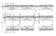
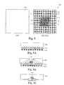
- FIG. 8illustrates several leadframes on a strip that is used by the processes illustrated in FIGS. 1 and 2 to fabricate the semiconductor packages illustrated in FIGS. 5 , 6 and 7 .
- FIG. 9illustrates a close up view of a portion of the strip of leadframes illustrated in FIG. 8 .
- FIGS. 10A-B , 11 A-B, 12 A-B, 13 A-B, 14 A-B, 15 A-B, and 16 A-Billustrate exemplary wire bond style semiconductor packages that are manufactured according to some embodiments of the invention.
- FIGS. 17A-B , 18 A-B, 19 A-B, and 20 A-Billustrate exemplary flip chip style packages manufactured according to some embodiments of the invention.
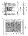
- FIG. 21illustrates an array of contact pads and connecting bars of a leadframe that is suitable for laser cutting or blade sawing the connecting bars to separate the contact pads from each other and from the die pad.
- FIG. 23illustrates possible paths of a saw blade to remove a set of connecting bars to separate the contact pads in the array of the leadframe illustrated in FIG. 21 .
- a “no lead” or leadless packagetypically contains a semiconductor die, a die pad, several bonding wires, and metal contacts or leads.
- the die pad and metal contactsare typically provided by a leadframe.
- the dieis preferably bonded to the die pad by using an adhesive, such as, for example, an epoxy.
- the bond wirestypically couple the die to one or more of the metal contacts.
- the dieis often contacted electrically through the bonding wires and/or the die pad.
- the die, die pad, and bonding wiresare encapsulated by using a plastic molding compound.
- the metal contacts in a leadless packagetypically do not extend beyond the dimensions of the package. However, the metal contacts typically are only partially encapsulated.
- Partial encapsulationleaves a portion, for example, a bottom side of the metal contacts exposed.
- Some no lead packagesalso have the bottom side of the die pad exposed.
- the no lead packageis usually mounted on a board such as a PCB, with the exposed surfaces of the metal contacts and/or die pad soldered to the bonding pads on the PCB.
- a no lead packagesuch as, for example, a quad flat no lead (QFN) package
- QFNquad flat no lead
- the metal leadsare generally nearly flush with a surface of the encapsulation.
- Another type of no lead package known in the industryis the dual flat no lead (DFN) package.
- the exposed or unmasked regions of the metal layerare plated.
- the platingcomprises nickel (Ni), palladium (PD), and gold (Au).
- Ninickel
- PDpalladium
- Augold
- the platingbinds to the areas of the metal layer that are not covered by the plating mask to yield a plated leadframe design on the metal layer.
- FIG. 1Aillustrates the metal layer 106 , having the plated regions 116 , 117 and an unplated masked region 118 .
- the plated region 116forms a die pad, while the plated region 117 forms a contact pad of a leadframe.
- the unplated regions 118are then typically used to form the connecting bars of some embodiments. As shown in FIG. 1 , once the metal layer is plated at the step 115 , the pre-tape process transitions to the step 120 .
- a top surface of the connecting bar 126is recessed with respect to the top surfaces of the die pad 116 and the contact pad 117 .
- the connecting bar 126is referred to as half-etched, in some embodiments. After the metal layer 106 is half etched to yield the connecting bar 126 , the pre-tape process transitions to the step 130 , illustrated in FIG. 1 .
- an adhesive tape 131is applied to the bottom side of the metal layer 106 .
- Some embodimentsemploy a polyimide tape in conjunction with an adhesive.
- the adhesiveis either silicone, or a thermoset polymer, such as an acrylic thermoset polymer, in these embodiments.
- FIG. 1Aillustrates an adhesive tape 131 pre-taped or adhered to the bottom side of the metal layer 106 , by using the adhesive.
- an overmolding 146is applied to encapsulate the die 141 , wire bond(s) 142 , and other portions of the leadframe.
- the adhesive tape 131is typically removed by using a de-taping procedure. As shown in FIG. 1A , the de-taping procedure exposes the unencapsulated bottom side of the metal layer 106 , particularly the bottom sides of the plated leadframe and the connecting bar(s) 126 .
- a pattern for removal of the connecting bars and/or isolation of the contact padsis selected. Further, a method of removal is selected at the step 155 of some embodiments. Then, the process 100 of FIG. 1 transitions to the step 160 , where the exposed (unplated) regions on a bottom side of the metal layer 106 (of FIG. 1A ), particularly the connecting bars 126 , are removed. Some embodiments remove the connecting bars in specific patterns, for instance, to isolate the contact pads based on the pattern selected at the step 155 . Further, some embodiments employ the method of removal selected at the step 155 . For instance, the metal layer 106 (of FIG. 1A ), and thus, the connecting bars 126 typically comprise unplated bare copper.
- the connecting bars 126are etched away in the embodiments that select and use an alkaline-type chemical etchant, such as, for example, ammonium hydroxide or ammonium chloride.
- an alkaline-type chemical etchantsuch as, for example, ammonium hydroxide or ammonium chloride.
- the chemical etchant of these embodimentsare specific to copper and do not significantly affect the regions of the metal layer 106 , that are plated by using nickel, palladium, gold, and/or various alloys, for example.
- the connecting bars 126 of some embodimentsare removed differently, for example, by using laser etching and/or blade sawing. These embodiments are further described in Section IV. Regardless of how the connecting bars 126 are removed, the plated die pad 116 and contact pads 117 of the leadframe are typically exposed, and can even protrude from the plastic molding 146 , at the bottom side of the encapsulated package, as shown in FIG. 1A . Then, the pre-tape process 100 concludes.
- FIG. 2illustrates semiconductor package fabrication with a no pre-tape process 200 .
- the no pre-tape process 200is sometimes also referred to as a tape or film “assist” molding process.
- the no pre-tape process 200begins at the step 205 , where a metal layer 206 is formed.
- the steps 205 through 225 of the no pre-tape process 200are substantially similar to the steps 105 through 125 of the pre-tape process 100 describe above.
- the molding machine employed by the no pre-tape process 200typically does not use an adhesive, but instead uses a vacuum suction to adhere the vacuum tape 243 against the bottom side of the metal layer 206 . Then, at the step 245 , the die pad and the contact pads of the leadframe are encapsulated. The molding machine of these embodiments typically performs the encapsulation by using a plastic polymer compound 246 . The molding machine also removes the vacuum tape 243 at the step 250 . De-taping of the vacuum tape 243 is often easily accomplished by releasing the vacuum suction holding the vacuum tape 243 in place. The vacuum tape 243 prevents the plastic molding from encapsulating the bottom side of the metal layer 206 . Thus, when the vacuum tape is removed at the step 250 , the bottom surface of the leadframe, particularly any unplated connecting bars 226 , are exposed.
- a pattern for removal of the connecting bars and/or isolation of the contact padsis selected. Further, a method of removal is selected at the step 255 of some embodiments. Then, the no pre-tape process 200 of FIG. 2 transitions to the step 260 , where the exposed (unplated) regions on a bottom side of the metal layer 206 (of FIG. 2A ), particularly the connecting bars 226 , are removed. Some embodiments remove the connecting bars 226 in specific patterns, for instance, to isolate the contact pads based on the pattern selected at the step 255 . Further, some embodiments employ the method of removal selected at the step 255 .
- the step 260 of the no pre-tape process 200leaves the plated surfaces of the die pad 216 and contact pads 217 not only exposed, but protruding from the bottom side of the semiconductor package. After the connecting bars are removed at the step 260 , the no pre-tape process 200 concludes.
- some embodimentsapply solder to the bottom side of the package by inverting the metal layer 306 and placing a stencil (not shown) over the bottom surface of the metal layer 306 .
- the stencilis typically a standless-type metal stencil that has openings for each of the exposed and/or protruding portions of the leadframe.
- the stencilhas openings for each of the contact pads 317 and the die pad 316 .
- a layer of solder pasteis wiped across the stencil. Accordingly, the solder paste is forced into the openings in the stencil, and when the stencil is removed, a set of solder balls 307 remain on each of the contact pads 317 and the die pad 316 .
- the stencil of some embodimentshas a single opening over the die pad, which causes a small layer of solder to be formed on the die pad, instead of the solder balls 507 illustrated in FIG. 5 .
- An exemplary product of these embodimentsis illustrated in FIG. 6 and slice views 6 A- 6 C.
- the die pad 616 of an exemplary BGA 600has a layer of solder 616 A instead of the solder balls.
- the BGA processtransitions to the step 365 of FIG. 3 , where the package is singulated from the molded sheet (or strip) of packages by using a singulation procedure.
- Singulationis performed differently in different embodiments. For example, some embodiments perform singulation by punching, while some embodiments perform dicing. Dicing includes sawing with a blade and/or cutting with a laser.
- the BGS process 300concludes. Singulation is discussed further in relation to FIG. 4 .
- FIG. 7illustrates an exemplary LGA package produced by using the LGA process 400 illustrated in FIG. 4 .
- the LGA package 700has a top and bottom with an exposed plated die pad 716 and contact pads 717 that protrude from the bottom of the LGA package 700 .
- the exemplary LGA package 700 illustrated in FIG. 7 and additional exemplary embodiments of the inventionare further described below in the next section.
- FIG. 7includes a bottom view of a semiconductor package 700 in accordance with some embodiments of the invention.
- the package 700is exemplary of several packages produced by the fabrication processes 100 and 200 discussed above.
- Cross section (slice) view 7 Ais a slice of the package 700 at line A-A
- slice view 7 Bis a slice along line B-B
- slice view 7 Cis a slice along line C-C.
- the package 700contains a die pad 716 and several exemplary rows of contact pads 717 around the die pad 716 .
- FIG. 7Aillustrates a metal plating 718 covers the top and bottom surfaces of the die pad 716 and the contact pads 717 , as described above.
- a die 741is typically mounted on the die pad 716 by means of an epoxy layer 719 , and bonding wires 742 extend from terminals (not shown) on the die 741 to various contact pads 717 .
- each bonding wire 742couples a terminal on the die 741 to a contact pad 717 .
- a protective molding 746encapsulates the die 741 , the bonding wires 742 , and the top portions of a leadframe comprising the die pad 716 and the contact pads 717 .
- the bottom surface of the molding 746is located at approximately the midpoint of the thickness of the die pad 716 and the contact pads 717 , as a result of the encapsulation, half etching, and taping steps of the processes 100 and 200 described above. This feature of the fabricated package is illustrated by slice views 7 A- 7 C.
- the bottom surface of the molding 746has a series of recesses 747 , which are formed at locations where the connecting bars (not shown) between a pair of neighboring contact pads 717 , and between the die pad 716 and a contact pad 717 are removed by etching, sawing, cutting, or by other means.
- flip-chip style semiconductor packageIn the flip-chip package, the die face is directly soldered or otherwise electrically connected to the die pad and/or one or more contact pads, rather than wire bonded. Flip-chip style packages are further described in relation to FIGS. 17A-20B below.
- FIG. 9illustrates that the die pad 916 and its adjacent contact pads 917 are joined by connecting bars 926 , and that each pair of the contact pads 917 are joined by a connecting bar 926 .
- the connecting bars 926 of some embodimentsare half etched such that the thickness of the connecting bars 926 is roughly half the thickness of the die pad 916 and the contact pads 917 .
- the connecting bars 926are shown without shading to illustrate this feature.
- the die pad 916 and the contact pads 917are shown with gray shading to indicate that they are both thicker and have metal plated surfaces.
- the die pad 916 and a set of nearby contact pads 917are bordered by a plated region 970 .
- the plated region 970is typically severed during singulation to yield an individual semiconductor package.
- Slice views 9 A and 9 Billustrate in detail that the half etching steps 125 and 225 (of FIGS. 1 and 2 , respectively), have formed the connecting bars 926 by half etching the top of a metal layer 906 .
- the metal layer 906 of some embodimentsis formed from a copper sheet.
- the connecting bars 926 of these embodimentsare some fraction of the thickness of the copper sheet.
- the connecting bars 926are substantially half the thickness of the copper sheet.
- the plated region 970 , the die pad 916 , and the contact pads 917have been masked (in the steps 120 and 220 of FIGS. 1 and 2 ) and thus remain at the full thickness of the original metal layer.
- FIGS. 10A-20BA wide variety of leadframes and resulting packages can be produced by the methods described above. Some examples of the variety of packages are illustrated in FIGS. 10A-20B .
- the “A” drawingis a cross-section (or “slice”) view of the package shown in the “B” drawing.
- the “B” drawingis a bottom view of each package.
- a slice viewcontains no background features that may lie behind the plane of the slice, whereas a cross section view may contain features of the background plane, that are not in the slice plane.
- FIGS. 13A and 13Billustrate a QFN package 1300 that is similar to the package 1000 (illustrated in FIGS. 10A and 10B ) except that a shelf is formed around the edges of the die pad 1316 .
- Some embodimentsform the shelf by using the masking, plating, and etching steps in the processes 100 and 200 (of FIGS. 1 and 2 , respectively), such that the die pad 1316 has a top surface larger than its bottom surface. For instance, some embodiments plate a large area on the top surface of a metal sheet and plate a smaller area below the large area on the bottom surface of the metal sheet. These embodiments then remove the unplated regions around the large and small plated areas to form the shelf shaped die pad 1316 illustrated in FIGS. 13A and 13B . As mentioned, the removal of the unplated regions is performed by chemical etching, with a laser, or with a saw blade.
- FIGS. 14A and 14Billustrate a dual flat no-lead (DFN) package 1400 with two rows of three contact pads 1417 on opposite sides of the package 1400 .
- the contact pads 1417are half-etched at the same time that the connecting bars are removed to form a shelf 1417 A on the interior end of each contact pad 1417 .
- the package 1400does not include a die pad, and the die 1441 is mounted with a layer of epoxy directly onto the shelf 1417 A of each of the contact pads 1417 .
- FIGS. 16A and 16Billustrate a QFN package 1600 that is similar to the package 1000 (illustrated in FIGS. 10A and 10B ) except that slots are formed in the die pad 1616 and the areas around each of the slots are half-etched to form half thick contact pads 1617 A that are coplanar with the bottom of the molding 1646 and are thus exposed at the bottom of the package 1600 , but that are not coplanar with the protruding plated regions of the die pad 1616 and the full thickness contact pads 1617 . Some embodiments form the half thick contact pads 1617 A during the same process step in which the connecting bars are removed.
- FIGS. 18A and 18Billustrate a QFN package 1800 that is similar to the package 1700 of FIG. 17 , except that the die pad 1716 is omitted.
- All of the packages illustrated in FIGS. 10A-20Bare fabricated by using one or more leadframes having connecting bars between the contact pads, and between the contact pads and the die pad (for those packages that include a die pad).
- the connecting barsare removed by chemical etching.
- the connecting barsare removed by other techniques, such as by laser cutting or etching, and/or by blade sawing. These techniques are described further in the next section.
- the generic grid array arrangement 2100 of some embodimentsis mass produced on quantities of metal sheets or strips. Some embodiments then later customize the quantities of the arrangement 2100 into the specific packages illustrated in Section III by using specific customization techniques. These techniques are similar to a singulation process used to separate the individual finished semiconductor devices and/or packages, and often occur prior to, or during, the singulation process. Some of these techniques are discussed below.
- the laser of some embodimentshas the particular advantages of spot cutting and/or cutting along a precise line.
- the laseralso has a drawback related to over-burning of the encapsulant compound.
- some embodimentsavoid (re) crossing a cut line or double spot cutting within the same area when using a laser, in order to prevent over-burning.
- FIG. 23illustrates that some embodiments use a saw blade to remove the connecting bars forming the array pattern 2100 illustrated in FIG. 21 .
- FIG. 23illustrates a possible set of paths of a saw blade that is used to remove one or more of the connecting bars 2326 from the arrangement 2300 , illustrated in FIG. 23 , to produce a customized package.
- the blade sawing, and chemical or laser etching, described in relation to FIGS. 21-23are often performed in conjunction with the singulation steps 365 and 465 of FIGS. 3 and 4 , respectively.
- the removal of the connecting barsis performed in conjunction with the steps 155 , 160 and 255 , 260 of FIGS. 1 and 2 , respectively, or at other times in additional embodiments of the invention.
- the pre-tape (adhesive) processhas particular advantages, while in some instances the no pre-tape (vacuum) process has particular advantages.
- the semiconductor package design and/or the leadframe structureare factors in determining whether the pre-tape or the no pre-tape process is preferred.
- the structure of some package designsincludes the contact pad and/or die pad patterns) causes the leadframe to have less structural strength.
- a structurally weak leadframeundesirably causes difficulty in handling the leadframes and semiconductor packages before encapsulation, and particularly during the wire bonding process. Errors during wire bonding and mishandling due to weak leadframes lowers the useful yield of the manufactured packages, and further undesirably causes quality issues in the finished product.
- both the pre-tape and no pre-tape processesare serviceable for all leadframe patterns and designs, but if the connecting bars are thin and/or form weak structural integrity, the pre-tape helps to hold the whole leadframe structure together for handling and wire bonding.
- the more reliable leadframe structureprovides better overall manufacturing yield, and quality.
- the pre-tape processprovides additional structural integrity to the strips of leadframes, which makes the leadframes easier to handle and improves wire bonding, yield, and quality.
- the connecting barsare sufficiently thick and strong to make the no pre-tape (vacuum) process a preferable alternative.
- the connecting barsare thick enough or there are many connecting bars, then there is no significant difference in quality and yield between the pre-tape and no pre-tape processes.
- the no pre-tape processgenerally has lower cost, since the tape is reusable and no adhesive is consumed. Thus, in these cases, the no pre-tape process is preferred.
- both the connecting bars and the tapeprovide support for the leadframe before encapsulation. Then, both the (adhesive) pre-tape and the connecting bars are removed after encapsulation when they are no longer needed.
- the pattern and/or shape of the connecting barsis related to the pattern and/or shape of the contact pads.
- the contact pads and connecting barsare designed to match such constraints as the position of the terminals of the die(s) and the physical requirements of the wire bonds.
- Section IIIillustrates a variety of different packages, having a myriad of patterns, contact pads, die pads, wire bonds, terminals, and their combinations, as contemplated in various embodiments of the invention.
- the description and illustrations aboveprovide many examples of several embodiments, including various manufacturing stages, such as, for example, leadframe conception and design, leadframe (die and contact pad) fabrication, wire bonding, encapsulation, connecting bar removal and or contact pad isolation, and singulation, in accordance with the invention.
Landscapes
- Engineering & Computer Science (AREA)
- Computer Hardware Design (AREA)
- Microelectronics & Electronic Packaging (AREA)
- Power Engineering (AREA)
- Physics & Mathematics (AREA)
- Condensed Matter Physics & Semiconductors (AREA)
- General Physics & Mathematics (AREA)
- Manufacturing & Machinery (AREA)
- Geometry (AREA)
- Lead Frames For Integrated Circuits (AREA)
Abstract
Description
- This application is a divisional application of co-pending U.S. patent application Ser. No. 12/154,483, filed on May 22, 2008, and entitled “Method and Apparatus for No Lead Semiconductor Package.” The co-pending U.S. patent application Ser. No. 12/154,483, filed on May 22, 2008, and entitled “Method and Apparatus for No Lead Semiconductor Package,” is hereby incorporated by reference.
- The present invention relates to no lead semiconductor packages. More specifically, the present invention is related to method and apparatus for no lead semiconductor package.
- A leaded semiconductor package typically has a semiconductor die encapsulated in molded plastic. The plastic encapsulation protects the die from physical damage as well as environmental effects, such as heat, light and/or electricity, for example. The leaded semiconductor package is typically mounted on a board, such as a printed circuit board (PCB), by means of metal leads that protrude from the encapsulation. The metal leads further provide electrical connections from the die to external circuitry that is typically located on the board. For instance, the metal leads are usually soldered or are otherwise electrically bonded to several bonding pads on the PCB.
- As described below, so called “leadless” or “no lead” semiconductor packages have also been developed. Many of these semiconductor packages are mass produced by using sheets of leadframe arrays. Leadframes provide a design and preliminary framework for the die pad and/or contact pads of a semiconductor package. However, leadframe technology has had difficulties in forming multi row terminals for leadless packages. For instance, half etching is conventionally used to form leadframes, and to form the connecting bars between the parts of the leadframe, and between the leadframes, themselves. This method of manufacture is often referred to as etched leadframe technology. However, etched leadframes can pose problems during manufacture, particularly during the handling and wire bonding processes. These problems relate to the strength and structural integrity of the leadframes, and thus, have adverse effects on useful yield and quality of the manufactured product.
- Accordingly, an additional plastic substrate, which is similar to a PCB, is conventionally used to provide additional strength and structure during manufacture, particularly for leadless packages having multiple rows of contact pads. However, the additional substrate undesirably adds cost, time delay, and other manufacturing problems.
- Embodiments of the invention provide a leadless semiconductor package. A method of fabricating the semiconductor package includes a process for forming a leadframe. The leadframe includes several contact pads and/or a die pad. Preferably, the lead frame further includes one or more connecting bar(s) that are formed between two or more contact pads, between a contact pad and a die pad, and/or between a contact pad and/or a die pad and an exterior portion of the leadframe. The exterior portion of the leadframe is not typically part of the completed semiconductor package.
- Specifically, some embodiments fabricate the lead frame by partially etching the top surface of a metal sheet to form the upper portions of the die pad, the contact pads, and/or the connecting bars of the leadframe. The bottom surface of the metal sheet is then etched to form the lower portions of the die pad, the contact pads, and the connecting bar(s). Before the surfaces of the metal sheet are etched, some embodiments apply a masking pattern to the surfaces of the metal sheet. The masking pattern typically covers the areas where the contact pads and/or the die pad of the leadframe are to be formed. In some embodiments, the masking pattern comprises a leadframe design. In some of these embodiments, the regions of the metal sheet for the connecting bar(s) are left unmasked or exposed to the etching process. Thus, in a leadframe of some embodiments, the etching process leaves the upper surfaces of the connecting bars recessed with respect to the upper surfaces of the die pad and/or contact pads, while the etching process in these, or in other embodiments, leaves the lower surfaces of the connecting bars coplanar with the lower surfaces of the die pad and/or contact pads.
- After the leadframe has been fabricated, a semiconductor die is typically attached to the die pad and the die is wire bonded to one or more contact pad(s) and/or the die pad. Alternatively, the connections between the die and the contact pads and/or the die pad are formed in other ways. For example, in a “flip-chip” style package, the semiconductor die is inverted, with the terminals of the die facing the die pad and/or the contact pads, such that the die terminals are soldered directly to the die pad and/or the contact pads, for example, with solder balls.
- After the electrical connections are formed between the semiconductor die and the die pad and/or the contact pads of the leadframe during wire bonding, the die and leadframe are encapsulated. Typically, encapsulation is performed by using a polymer molding compound. During the encapsulation process of some embodiments, the lower surfaces of the leadframe, including the die pad, contact pads, and/or one or more connecting bar(s) are attached to, or held against, a tape to prevent the molding compound from encapsulating the lower surfaces of the die pad, contact pads, and/or the connecting bars. However, the molding compound encapsulates the top surfaces of the leadframe and fills any areas between the components of the leadframe, such as the connecting bars, for example.
- After the encapsulation process, the molding tends to hold the semiconductor package together. Thus, the connecting bars of some embodiments are no longer needed and are removed. The connecting bars of some of these embodiments are exposed at the bottom surface of the package. The removal of these connecting bars is performed by using various methods, such as, for example, chemical etching, and/or cutting with a laser or a saw blade. During this “isolation” step, one or more contact pad(s) are isolated by the etching, cutting and/or sawing. In some embodiments, the connecting bars are removed based on a specific pattern that is selected for the semiconductor package. In some embodiments, the means for removal of the connecting bars is also selected based on the selected pattern for the semiconductor package.
- After the connecting bars are removed and/or the contact pads are isolated, the semiconductor packages are then singulated to separate individual semiconductor packages from the molded sheet of semiconductor packages. Singulation is typically performed by using a dicing saw to make cuts along the edges of the packages. In the singulation process, any connecting bars that run along the edges of the packages are severed.
- The novel features of the invention are set forth in the appended claims. However, for purpose of explanation, several embodiments of the invention are set forth in the following figures.
FIG. 1 illustrates a pre-tape process for semiconductor package fabrication.FIG. 1A illustrates an exemplary result produced by each step of the pre-tape process ofFIG. 1 .FIG. 2 illustrates a no pre-tape process for semiconductor package fabrication.FIG. 2A illustrates an exemplary result produced by each step of the no pre-tape process ofFIG. 2 .FIG. 3 illustrates the additional steps required to fabricate a ball grid array package.FIG. 3A illustrates an exemplary result produced by each step of the BGA process ofFIG. 3 .FIG. 4 illustrates the additional steps required to fabricate a leadless grid array package.FIG. 4A illustrates an exemplary result produced by each step of the LGA process ofFIG. 4 .FIG. 5 illustrates multiple views of a BGA with a die pad having solder balls produced by the BGA process ofFIG. 3 .FIG. 6 illustrates multiple views of a BGA with a die pad having a solder layer instead of solder balls.FIG. 7 illustrates multiple views of an LGA produced by the LGA process illustrated inFIG. 4 .FIG. 8 illustrates several leadframes on a strip that is used by the processes illustrated inFIGS. 1 and 2 to fabricate the semiconductor packages illustrated inFIGS. 5 ,6 and7.FIG. 9 illustrates a close up view of a portion of the strip of leadframes illustrated inFIG. 8 .FIGS. 10A-B ,11A-B,12A-B,13A-B,14A-B,15A-B, and16A-B, illustrate exemplary wire bond style semiconductor packages that are manufactured according to some embodiments of the invention.FIGS. 17A-B ,18A-B,19A-B, and20A-B illustrate exemplary flip chip style packages manufactured according to some embodiments of the invention.FIG. 21 illustrates an array of contact pads and connecting bars of a leadframe that is suitable for laser cutting or blade sawing the connecting bars to separate the contact pads from each other and from the die pad.FIG. 22 illustrates possible cutting paths of a laser to remove connecting bars to separate the contact pads in the array of the leadframe illustrated inFIG. 21 .FIG. 23 illustrates possible paths of a saw blade to remove a set of connecting bars to separate the contact pads in the array of the leadframe illustrated inFIG. 21 .- In the following description, numerous details and alternatives are set forth for purpose of explanation. However, one of ordinary skill in the art will realize that the invention can be practiced without the use of these specific details. In other instances, well-known structures and devices are shown in block diagram form in order not to obscure the description of the invention with unnecessary detail.
- A “no lead” or leadless package typically contains a semiconductor die, a die pad, several bonding wires, and metal contacts or leads. The die pad and metal contacts are typically provided by a leadframe. The die is preferably bonded to the die pad by using an adhesive, such as, for example, an epoxy. Additionally, the bond wires typically couple the die to one or more of the metal contacts. The die is often contacted electrically through the bonding wires and/or the die pad. The die, die pad, and bonding wires are encapsulated by using a plastic molding compound. In contrast to a leaded package, the metal contacts in a leadless package typically do not extend beyond the dimensions of the package. However, the metal contacts typically are only partially encapsulated. Partial encapsulation leaves a portion, for example, a bottom side of the metal contacts exposed. Some no lead packages also have the bottom side of the die pad exposed. The no lead package is usually mounted on a board such as a PCB, with the exposed surfaces of the metal contacts and/or die pad soldered to the bonding pads on the PCB. Thus in a no lead package such as, for example, a quad flat no lead (QFN) package, the metal leads are generally nearly flush with a surface of the encapsulation. Another type of no lead package known in the industry is the dual flat no lead (DFN) package.
- The no lead packages described above are sometimes manufactured by attaching a plurality of dies to several corresponding die pads in one or more leadframes on a metal sheet. In some instances, the metal contacts and the die pad of each leadframe are connected by an array of connecting bars. The leadframe is often attached to a tape. The tape is typically an adhesive tape that temporarily provides the die pad, metal contacts, and lead frame temporary support during wire bonding. The tape provides support in conjunction with, or instead of, the connecting bars. After the electrical connections have been made between the die and the metal contacts during wire bonding or otherwise, the die(s) and die pad(s) are then encapsulated in a plastic molding compound and the tape is removed. The connecting bars are also removed. In some embodiments, the connecting bars are severed by a novel process involving a laser and/or a blade saw. Preferably, the connecting bars are removed in specific patterns, for example, to isolate specific contact pads and/or one or more die pad(s) in particular configurations.
- Once the contact pads and/or die pad(s) are isolated in the desired configurations, the encapsulated packages are separated from the molded sheet or molded strip of dies and/or leadframes by a singulation process to produce individual manufactured semiconductor packages. Various methods of manufacturing no lead packages are described in Section II. The products of some of these methods are described in Section III.
- A. The Pre-Tape Process
FIG. 1 illustrates semiconductor package fabrication with a pre-tape process100. As shown in this figure, the pre-tape process100 begins at thestep 105, where a metal layer is formed. Preferably, the metal layer is formed from a sheet of bare copper or some other metal, such as Alloy 42. For instance,FIG. 1A illustrates ametal layer 106, fanned by thestep 105 illustrated inFIG. 1 .- Then, as shown in
FIG. 1 , the pre-tape process100 transitions to thestep 110, where a plating-mask is applied to the metal layer. The plating mask typically comprises a leadframe design that is formed using a photo resist pattern. Leadframe designs are discussed further in Section III. The photo resist pattern covers areas of the metal layer that are not to be plated, for example, the areas between a die pad and several contact pads of a leadframe, and the areas on the metal layer that are between lead frames. Once the plating mask is applied to the metal layer at thestep 110, the pre-tape process transitions to thestep 115. - At the
step 115, the exposed or unmasked regions of the metal layer are plated. In some embodiments, the plating comprises nickel (Ni), palladium (PD), and gold (Au). However, one of ordinary skill will recognize other platings, such as, for example, Ni/Pd/Au-alloy, Ni/Au, or Ni/Au-alloy. As mentioned above, the plating binds to the areas of the metal layer that are not covered by the plating mask to yield a plated leadframe design on the metal layer. For instance,FIG. 1A illustrates themetal layer 106, having the platedregions masked region 118. Specifically, the platedregion 116 forms a die pad, while the platedregion 117 forms a contact pad of a leadframe. Theunplated regions 118 are then typically used to form the connecting bars of some embodiments. As shown inFIG. 1 , once the metal layer is plated at thestep 115, the pre-tape process transitions to thestep 120. - At the
step 120, an etch mask is applied to the plated regions of the metal layer. The etch mask is typically a photo resist material that prevents the leadframe design formed above (at the step115) from being etched away at thestep 125. - At the
step 125, the exposed (unmasked) regions on a top side of the metal layer are etched away to yield connecting bars between the components of the leadframe, such as the die pad and the contact pads, formed above (at the step115). Some embodiments employ a cupric chloride etchant to etch away a top portion of the metal layer between the die pad and the contact pads. These embodiments form a connecting bar between the die pad and the contact pads of the leadframe. For instance,FIG. 1A illustrates themetal layer 106 with a connectingbar 126 formed by etching the unmasked region between thedie pad 116 and thecontact pad 117. As shown in this figure, a top surface of the connectingbar 126 is recessed with respect to the top surfaces of thedie pad 116 and thecontact pad 117. Thus, the connectingbar 126 is referred to as half-etched, in some embodiments. After themetal layer 106 is half etched to yield the connectingbar 126, the pre-tape process transitions to thestep 130, illustrated inFIG. 1 . - At the
step 130 of the pre-tape process100, anadhesive tape 131 is applied to the bottom side of themetal layer 106. Some embodiments employ a polyimide tape in conjunction with an adhesive. The adhesive is either silicone, or a thermoset polymer, such as an acrylic thermoset polymer, in these embodiments. For instance,FIG. 1A illustrates anadhesive tape 131 pre-taped or adhered to the bottom side of themetal layer 106, by using the adhesive. - Then, as shown by the
steps FIGS. 1 and 1A , adie 141 is attached to thedie pad 116, and thedie 141 is wire bonded142 to thedie pad 116 and/or the contact pad(s)117 of the lead frame. - Next, at the
step 145, anovermolding 146 is applied to encapsulate thedie 141, wire bond(s)142, and other portions of the leadframe. At thestep 150, theadhesive tape 131 is typically removed by using a de-taping procedure. As shown inFIG. 1A , the de-taping procedure exposes the unencapsulated bottom side of themetal layer 106, particularly the bottom sides of the plated leadframe and the connecting bar(s)126. - At the
step 155, of some embodiments, a pattern for removal of the connecting bars and/or isolation of the contact pads is selected. Further, a method of removal is selected at thestep 155 of some embodiments. Then, the process100 ofFIG. 1 transitions to thestep 160, where the exposed (unplated) regions on a bottom side of the metal layer106 (ofFIG. 1A ), particularly the connectingbars 126, are removed. Some embodiments remove the connecting bars in specific patterns, for instance, to isolate the contact pads based on the pattern selected at thestep 155. Further, some embodiments employ the method of removal selected at thestep 155. For instance, the metal layer106 (ofFIG. 1A ), and thus, the connectingbars 126 typically comprise unplated bare copper. Hence, the connectingbars 126 are etched away in the embodiments that select and use an alkaline-type chemical etchant, such as, for example, ammonium hydroxide or ammonium chloride. The chemical etchant of these embodiments are specific to copper and do not significantly affect the regions of themetal layer 106, that are plated by using nickel, palladium, gold, and/or various alloys, for example. - Moreover, the connecting
bars 126 of some embodiments are removed differently, for example, by using laser etching and/or blade sawing. These embodiments are further described in Section IV. Regardless of how the connectingbars 126 are removed, the plateddie pad 116 andcontact pads 117 of the leadframe are typically exposed, and can even protrude from theplastic molding 146, at the bottom side of the encapsulated package, as shown inFIG. 1A . Then, the pre-tape process100 concludes. - B. The No Pre-Tape or the “Tape Assist” Process
- Some embodiments employ a different process to fabricate the leadframe and package. For instance,
FIG. 2 illustrates semiconductor package fabrication with a no pre-tape process200. The no pre-tape process200 is sometimes also referred to as a tape or film “assist” molding process. As shown inFIG. 2 , the no pre-tape process200 begins at thestep 205, where ametal layer 206 is formed. As illustrated inFIGS. 2 and 2A , thesteps 205 through225 of the no pre-tape process200 are substantially similar to thesteps 105 through125 of the pre-tape process100 describe above. However, at thesteps FIG. 2 , the no pre-tape process200 diverges from the pre-tape process100. Specifically, as illustrated inFIGS. 2 and 2A , at thesteps die 241 is attached to adie pad 216 and wire bonded242 to thedie pad 216 and/or one or more contact pad(s)217 of the lead frame. As shown in these figures, the die attachstep 230 and thewire bonding step 235 occur before any taping occurs (at the step240). - At the
step 240, avacuum tape 243 is applied to a bottom side of themetal layer 206. Some embodiments apply thevacuum tape 243 by using a molding machine. Several molding machines have been used successfully with various embodiments of the invention. For instance, the following provides a representative list of some of the molding machines used in conjunction with the processes100 and200 described above: Fico i-series such as the AMS-i-204 and AMS-i-306; Fico M-series such as the AMS-24-M2 and AMS-36-M3; Fico W-series such as the AMS-24-M2 and AMS-36-M3; Boschman such as the Flexstar and Packstar; Towa Y-series such as the YPS, YFG, and YFT; Daiichi GP-Pro; and the ASM Ideal Mold machine. - Regardless of the particular model and supplier, the molding machine employed by the no pre-tape process200 typically does not use an adhesive, but instead uses a vacuum suction to adhere the
vacuum tape 243 against the bottom side of themetal layer 206. Then, at thestep 245, the die pad and the contact pads of the leadframe are encapsulated. The molding machine of these embodiments typically performs the encapsulation by using aplastic polymer compound 246. The molding machine also removes thevacuum tape 243 at thestep 250. De-taping of thevacuum tape 243 is often easily accomplished by releasing the vacuum suction holding thevacuum tape 243 in place. Thevacuum tape 243 prevents the plastic molding from encapsulating the bottom side of themetal layer 206. Thus, when the vacuum tape is removed at thestep 250, the bottom surface of the leadframe, particularly any unplated connectingbars 226, are exposed. - Then, at the
step 255, of some embodiments, a pattern for removal of the connecting bars and/or isolation of the contact pads is selected. Further, a method of removal is selected at thestep 255 of some embodiments. Then, the no pre-tape process200 ofFIG. 2 transitions to thestep 260, where the exposed (unplated) regions on a bottom side of the metal layer206 (ofFIG. 2A ), particularly the connectingbars 226, are removed. Some embodiments remove the connectingbars 226 in specific patterns, for instance, to isolate the contact pads based on the pattern selected at thestep 255. Further, some embodiments employ the method of removal selected at thestep 255. For instance, in some embodiments, the exposed (un-plated) regions on the bottom side of themetal layer 206 are etched or cut away. As mentioned above, etching is performed by using a laser or a chemical etchant that is specific to the unplated regions of themetal layer 206. As an example, ammonium hydroxide or ammonium chloride will etch away the unplated connectingbars 226, without significantly affecting thedie pad 216 and/or thecontact pads 217 that were plated by using nickel, palladium, and/or gold. Alternatively, the connecting bars are cut away, in some embodiments, by using a saw blade, a laser, or another cutting means. As mentioned above, the removal of the connectingbars 226 is discussed further in Section IV. - Thus, as further illustrated in
FIG. 2A , thestep 260 of the no pre-tape process200 leaves the plated surfaces of thedie pad 216 andcontact pads 217 not only exposed, but protruding from the bottom side of the semiconductor package. After the connecting bars are removed at thestep 260, the no pre-tape process200 concludes. - C. Additional Steps for LGA/BGA Fabrication
- Regardless of whether the semiconductor package is fabricated by using the pre-tape process100 or the no pre-tape process200 described above, the semiconductor package of some embodiments is finalized as a ball grid array (BGA) or as a leadless grid array (LGA). To fabricate the semiconductor package as a BGA, some embodiments employ the
BGA process 300 illustrated inFIG. 3 . As shown in this figure, theBGA process 300 begins at thestep 360, where solder is applied to the bottom side of the package. Thestep 360 ofFIG. 3 typically follows thestep 160 or thestep 260 ofFIGS. 1 and 2 , respectively. - As illustrated in
FIG. 3A , some embodiments apply solder to the bottom side of the package by inverting themetal layer 306 and placing a stencil (not shown) over the bottom surface of themetal layer 306. The stencil is typically a standless-type metal stencil that has openings for each of the exposed and/or protruding portions of the leadframe. For example, in the embodiment shown inFIG. 3A , the stencil has openings for each of thecontact pads 317 and thedie pad 316. With the stencil held against the exposed portions of the leadframe, a layer of solder paste is wiped across the stencil. Accordingly, the solder paste is forced into the openings in the stencil, and when the stencil is removed, a set ofsolder balls 307 remain on each of thecontact pads 317 and thedie pad 316. FIGS. 5-5C illustrate an exemplary BGA formed by using theBGA process 300 illustrated inFIG. 3 . As shown inFIG. 5 , theBGA 500 has a top and bottom, an exposeddie pad 516 andseveral solder balls 507 on thedie pad 516 and obscuring eachcontact pad 517. Thecontact pads 517 are more readily illustrated in cross section (slice) views5A and5B. Slice view5A illustrates a slice through a line ofsolder balls 507 attached to a set ofcontact pads 517. Slice view5B illustrates a slice through a line ofsolder balls 507 attached to a set ofcontact pads 517 and thedie pad 516. Slice view5C illustrates a slice of the package that is between two columns or rows ofsolder balls 507 that are attached to sets ofcontact pads 517, only.- Alternatively, the stencil of some embodiments has a single opening over the die pad, which causes a small layer of solder to be formed on the die pad, instead of the
solder balls 507 illustrated inFIG. 5 . An exemplary product of these embodiments is illustrated inFIG. 6 and slice views6A-6C. As shown inFIG. 6 , thedie pad 616 of anexemplary BGA 600 has a layer of solder616A instead of the solder balls. - Regardless of the solder's shape, once the solder is applied to the exposed die pad and contact pads of the leadframe, the BGA process transitions to the
step 365 ofFIG. 3 , where the package is singulated from the molded sheet (or strip) of packages by using a singulation procedure. Singulation is performed differently in different embodiments. For example, some embodiments perform singulation by punching, while some embodiments perform dicing. Dicing includes sawing with a blade and/or cutting with a laser. After thesingulation step 365, theBGS process 300 concludes. Singulation is discussed further in relation toFIG. 4 . FIG. 4 illustrates that the fabrication of an LGA does not require the step of applying solder paste or balls as described above in relation to BGA fabrication. As shown inFIG. 4 , the fabrication of an LGA requires only the addition of thesingulation step 465 after thestep 160 ofFIG. 1 , or thestep 260 ofFIG. 2 (removing the connecting bars). As illustrated inFIG. 4A , some platedregions 470 of themetal layer 406 extend beyond a single leadframe and/or extend beyond a single semiconductor package. The platedregions 470 of these embodiments allow the simultaneous fabrication of several leadframes and packages at once from a single metal sheet. These platedregions 470 are typically also removed during the singulation steps365 and465 illustrated inFIGS. 3 ,3A,4 and4A. Some embodiments employ a conventional dicing saw for the singulation step. Singulation is generally discussed in the co-owned U.S. Pat. No. 7,572,168, issued on Aug. 11, 2009, and entitled “METHOD AND APPARATUS FOR HIGH SPEED SINGULATION,” which is incorporated herein by reference.FIG. 7 illustrates an exemplary LGA package produced by using theLGA process 400 illustrated inFIG. 4 . As shown in this figure, theLGA package 700 has a top and bottom with an exposed plateddie pad 716 andcontact pads 717 that protrude from the bottom of theLGA package 700. Theexemplary LGA package 700 illustrated inFIG. 7 and additional exemplary embodiments of the invention are further described below in the next section.- A. Fabricated Package
- As mentioned above,
FIG. 7 includes a bottom view of asemiconductor package 700 in accordance with some embodiments of the invention. Thepackage 700 is exemplary of several packages produced by the fabrication processes100 and200 discussed above. Cross section (slice) view7A is a slice of thepackage 700 at line A-A, slice view7B is a slice along line B-B, and slice view7C is a slice along line C-C. Thepackage 700 contains adie pad 716 and several exemplary rows ofcontact pads 717 around thedie pad 716.FIG. 7A illustrates a metal plating718 covers the top and bottom surfaces of thedie pad 716 and thecontact pads 717, as described above. Also discussed above, the metal plating718 typically includes some combination of Ni/Pd/Au, and/or alloys thereof. As used herein, unless the context indicates otherwise, such directional terms as “top” and “bottom” refer to a package oriented with the exposed portion of the die pad and/or contact pads facing downward. However, one of ordinary skill will recognize the various different orientations of the exemplary semiconductor packages discussed herein. - As illustrated in
FIG. 7B , adie 741 is typically mounted on thedie pad 716 by means of anepoxy layer 719, andbonding wires 742 extend from terminals (not shown) on thedie 741 tovarious contact pads 717. Typically, eachbonding wire 742 couples a terminal on thedie 741 to acontact pad 717. Aprotective molding 746 encapsulates thedie 741, thebonding wires 742, and the top portions of a leadframe comprising thedie pad 716 and thecontact pads 717. In some embodiments, the bottom surface of themolding 746 is located at approximately the midpoint of the thickness of thedie pad 716 and thecontact pads 717, as a result of the encapsulation, half etching, and taping steps of the processes100 and200 described above. This feature of the fabricated package is illustrated by slice views7A-7C. - Specifically shown in slice view7C, the bottom surface of the
molding 746 has a series ofrecesses 747, which are formed at locations where the connecting bars (not shown) between a pair ofneighboring contact pads 717, and between thedie pad 716 and acontact pad 717 are removed by etching, sawing, cutting, or by other means. - One of ordinary skill will recognize variations in the packages and fabrication methods described above. For instance, some embodiments fabricate a “flip-chip” style semiconductor package. In the flip-chip package, the die face is directly soldered or otherwise electrically connected to the die pad and/or one or more contact pads, rather than wire bonded. Flip-chip style packages are further described in relation to
FIGS. 17A-20B below. - B. Leadframes
- As mentioned above, the semiconductor package typically includes a leadframe that was fabricated during the fabrication processes100 and200, discussed above. The leadframe is typically mass produced from a metal sheet to facilitate the fabrication of the semiconductor packages. For instance, the packages described above, such as the
package 700, for example, is fabricated by using a strip ofleadframes 800 illustrated inFIG. 8 . The leadframes in thestrip 800 are particularly suited to fabrication by using the pre-tape process100 and the no pre-tape process200. - The features of these leadframes are more apparent in the close up views of the
strip 800 that are provided byFIG. 9 . As shown inFIG. 9 , aparticular section 900 of thestrip 800 has sixdie pads 916, each surrounded byseveral contact pads 917. In some embodiments, thesection 900 forms a single leadframe in the strip ofleadframes 800, illustrated inFIG. 8 . In thesection 900, the close up view of thedie pad 916 and thecontact pads 917 in its vicinity represent a pre-cursor to grid arrays, such as the grid arrays in the LGA and BGA packages discussed above. Specifically,FIGS. 8 and 9 illustrate the leadframes at thesteps 125 and225 (the half etch steps) of the processes100 and200, respectively. - Thus,
FIG. 9 illustrates that thedie pad 916 and itsadjacent contact pads 917 are joined by connectingbars 926, and that each pair of thecontact pads 917 are joined by a connectingbar 926. As illustrated inFIG. 9 , the connectingbars 926 of some embodiments are half etched such that the thickness of the connectingbars 926 is roughly half the thickness of thedie pad 916 and thecontact pads 917. InFIG. 9 , the connectingbars 926 are shown without shading to illustrate this feature. In contrast to the unshaded connectingbars 926, thedie pad 916 and thecontact pads 917 are shown with gray shading to indicate that they are both thicker and have metal plated surfaces. - Further illustrated in the close up views of
FIG. 9 , thedie pad 916 and a set ofnearby contact pads 917 are bordered by a platedregion 970. As mentioned above in relation toFIGS. 3 and 4 , the platedregion 970 is typically severed during singulation to yield an individual semiconductor package. - Slice views9A and9B illustrate in detail that the
half etching steps 125 and225 (ofFIGS. 1 and 2 , respectively), have formed the connectingbars 926 by half etching the top of ametal layer 906. Themetal layer 906 of some embodiments is formed from a copper sheet. Thus, the connectingbars 926 of these embodiments are some fraction of the thickness of the copper sheet. Preferably the connectingbars 926 are substantially half the thickness of the copper sheet. However, the platedregion 970, thedie pad 916, and thecontact pads 917, have been masked (in thesteps FIGS. 1 and 2 ) and thus remain at the full thickness of the original metal layer. Moreover, as shown in the slice views9A and9B, the platedregion 970, thedie pad 916, and the contact pad(s)917 have been plated (at thesteps 115 and215) with some combination of Ni/Pd/Au, and/or one or more alloys thereof. - C. More Examples of Leadframes and Packages
- A wide variety of leadframes and resulting packages can be produced by the methods described above. Some examples of the variety of packages are illustrated in
FIGS. 10A-20B . In each pair of drawings, the “A” drawing is a cross-section (or “slice”) view of the package shown in the “B” drawing. The “B” drawing is a bottom view of each package. As used herein, a slice view contains no background features that may lie behind the plane of the slice, whereas a cross section view may contain features of the background plane, that are not in the slice plane. FIGS. 10A and 10B illustrate a quad flat no lead (QFN)package 1000 having threecontact pads 1017 on each side of acentral die pad 1016. TheQFN package 1000 is formed by using either of the pre-tape or no pre-tape processes (100 or200) described above. For instance, in theQFN package 1000, the region between thedie pad 1016 and thecontact pads 1017 is comparatively substantial (capable of sustaining several substantial connecting bars). Accordingly, the leadframe and connecting bars, which are the precursor for thepackage design 1000 illustrated inFIG. 10 , are likely sufficiently structurally for handling, and particularly during the wire bonding process. Hence, some embodiments will advantageously employ the no-pretape process200 to manufacture thepackage 1000. Further, some embodiments select the appropriate pattern for thepackage 1000 during the process200 and execute the design and/or pattern by using the various methods of masking, plating, etching, cutting, and/or sawing described above. The figures and description below provide additional examples.- For instance,
FIGS. 11A and 11B illustrate aQFN package 1100 with two rows of contact pads1117 around acentral die pad 1116. Specifically, the contact pads1117 in each row are offset from the contact pads in the other row. Due to this pattern of contact pads, thepackage 1100 has particular requirements for manufacture, and issues with structural integrity during handling and/or wire bonding. Hence, some embodiments will particularly employ the pre-tape process100 in conjunction with, or instead of, a set of connecting bars, during the manufacture of thepackage 1100. Additionally, some embodiments employ a set of thicker connecting bars for added strength. Moreover, some embodiments select a method of removal for the connecting bars that is appropriate to the pattern of multiple rows of offset contact pads, such as, for example, when the contact pad pattern presents difficulties for blade saw removal of the connecting bars.FIG. 11B illustrates such a case. In these cases, some embodiments advantageously employ laser etching and/or cutting to remove the connecting bars. FIGS. 12A and 12B illustrate aQFN package 1200 that is similar to the package1100 (inFIG. 11 ) except that thecontact pads 1217 are not offset from each other and there are four [large contact pads] at the corners of thepackage 1200. Here, as above, one of ordinary skill will recognize the particular applications of the processes100 and200 (ofFIGS. 1 and 2 ) to thepackage 1200 illustrated inFIG. 12 .FIGS. 13A and 13B illustrate aQFN package 1300 that is similar to the package1000 (illustrated inFIGS. 10A and 10B ) except that a shelf is formed around the edges of thedie pad 1316. Some embodiments form the shelf by using the masking, plating, and etching steps in the processes100 and200 (ofFIGS. 1 and 2 , respectively), such that thedie pad 1316 has a top surface larger than its bottom surface. For instance, some embodiments plate a large area on the top surface of a metal sheet and plate a smaller area below the large area on the bottom surface of the metal sheet. These embodiments then remove the unplated regions around the large and small plated areas to form the shelf shapeddie pad 1316 illustrated inFIGS. 13A and 13B . As mentioned, the removal of the unplated regions is performed by chemical etching, with a laser, or with a saw blade.FIGS. 14A and 14B illustrate a dual flat no-lead (DFN)package 1400 with two rows of threecontact pads 1417 on opposite sides of thepackage 1400. Preferably, thecontact pads 1417 are half-etched at the same time that the connecting bars are removed to form ashelf 1417A on the interior end of eachcontact pad 1417. Thepackage 1400 does not include a die pad, and thedie 1441 is mounted with a layer of epoxy directly onto theshelf 1417A of each of thecontact pads 1417.FIGS. 15A and 15B illustrate apackage 1500 that is similar to the package1400 (ofFIG. 14 ) except that a center bar runs between two contact pads located at opposite ends of thepackage 1500. Some embodiments form the center bar [in the same step in which the connecting bars are removed].FIGS. 16A and 16B illustrate aQFN package 1600 that is similar to the package1000 (illustrated inFIGS. 10A and 10B ) except that slots are formed in thedie pad 1616 and the areas around each of the slots are half-etched to form halfthick contact pads 1617A that are coplanar with the bottom of themolding 1646 and are thus exposed at the bottom of thepackage 1600, but that are not coplanar with the protruding plated regions of thedie pad 1616 and the fullthickness contact pads 1617. Some embodiments form the halfthick contact pads 1617A during the same process step in which the connecting bars are removed.FIGS. 17A-B ,18A-B,19A-B and20A-B, in particular illustrate “flip chip” style packages, in which the die is inverted and connections are made directly between the terminals on the die and the die pad and/or the contact pads. The connections are made with solder balls, in some embodiments. In each of the packages (1700,1800,1900,2000) illustrated in these figures, the interior end of each contact has a shelf, and the solder balls connect the upper surface of the shelf to the die pad.- Specifically,
FIGS. 17A and 17B illustrate aQFN package 1700 with adie pad 1716 surrounded bycontact pads 1717 each of which has ashelf 1717A. Terminals on thedie 1741 are connected to thedie pad 1716 and the contact pads1717 (including theshelves 1717A) by solder balls. FIGS. 18A and 18B illustrate aQFN package 1800 that is similar to thepackage 1700 ofFIG. 17 , except that thedie pad 1716 is omitted.FIGS. 19A and 19B illustrate aDFN package 1900 with no die pad and where theshelf 1917A of eachcontact pad 1917 is angled.FIGS. 20A and 20B illustrate aDFN package 2000 that is similar to theDFN package 1900 ofFIG. 19 except that theshelf 2017A on each of thecontact pads 2017 is straight.- All of the packages illustrated in
FIGS. 10A-20B are fabricated by using one or more leadframes having connecting bars between the contact pads, and between the contact pads and the die pad (for those packages that include a die pad). In some of the embodiments described above, the connecting bars are removed by chemical etching. Alternatively, the connecting bars are removed by other techniques, such as by laser cutting or etching, and/or by blade sawing. These techniques are described further in the next section. - Some embodiments employ a combination of connecting bar patterns, and plating, masking, and/or etching patterns, to form multiple rows of contact pads. Some of these embodiments select and/or match each pattern with an appropriate method of removing the connecting bars to isolate each contact pad as specified by the pattern. As mentioned above, the methods of removal include chemical and laser, etching or cutting, and blade sawing.
- A. Singulation and/or Etching Patterns
- The processes of Section II and the leadframes and packages of Section III particularly lend themselves to specific isolation and/or singulation patterns. For instance,
FIG. 21 illustrates aspecific arrangement 2100 of adie pad 2116 andcontact pads 2117 in an array of a leadframe that has a pattern that is different from the grid arrays illustrated above. Thisspecific arrangement 2100 has a particular pattern of connectingbars 2126 between thedie pad 2116 and itsadjacent contact pads 2117, and between certain pairs ofcontact pads 2117, such that a set of parallel “L” shaped paths are formed within a section bordered by a platedregion 2170. The particular patterns of some connecting bar arrays, such as the “L” shaped pattern ofFIG. 21 and the many configurations of packages illustrated in Section III, require specific fabrication techniques. - For instance, the generic
grid array arrangement 2100 of some embodiments is mass produced on quantities of metal sheets or strips. Some embodiments then later customize the quantities of thearrangement 2100 into the specific packages illustrated in Section III by using specific customization techniques. These techniques are similar to a singulation process used to separate the individual finished semiconductor devices and/or packages, and often occur prior to, or during, the singulation process. Some of these techniques are discussed below. - B. Laser Cutting or Etching
FIG. 22 illustrates that some embodiments use a laser to remove the connecting bars forming thearray pattern 2100 illustrated inFIG. 21 .FIG. 22 shows some possible paths of a laser beam that removes the connecting bars along the paths by laser etching or cutting. Each of the lines illustrated inFIG. 22 describes a square that is concentric about thedie pad 2216. As mentioned above, by removing particular connectingbars 2226 from the array or arrangement2200, in conjunction with the masking, plating, and/or etching steps described above, some embodiments produce the custom packages illustrated in Section III. The use of a laser in these embodiments has certain advantages in the targeted removal of particular connecting bars. For instance, the pattern of contact pads of some embodiment poses particular constraints. Some of these constraints were described in relation to theFIGS. 10A-20B above.- As shown in
FIG. 22 and theFIGS. 10A-20B described above, the laser of some embodiments has the particular advantages of spot cutting and/or cutting along a precise line. However, the laser also has a drawback related to over-burning of the encapsulant compound. Thus, some embodiments avoid (re) crossing a cut line or double spot cutting within the same area when using a laser, in order to prevent over-burning. - C. Blade Sawing
- Similarly,
FIG. 23 illustrates that some embodiments use a saw blade to remove the connecting bars forming thearray pattern 2100 illustrated inFIG. 21 . Thus,FIG. 23 illustrates a possible set of paths of a saw blade that is used to remove one or more of the connectingbars 2326 from the arrangement2300, illustrated inFIG. 23 , to produce a customized package. - As mentioned above, the blade sawing, and chemical or laser etching, described in relation to
FIGS. 21-23 are often performed in conjunction with the singulation steps365 and465 ofFIGS. 3 and 4 , respectively. Alternatively, the removal of the connecting bars is performed in conjunction with thesteps FIGS. 1 and 2 , respectively, or at other times in additional embodiments of the invention. - D. The Pre-Tape and No Pre-Tape Processes
- In some instances, the pre-tape (adhesive) process has particular advantages, while in some instances the no pre-tape (vacuum) process has particular advantages. In these various instances, the semiconductor package design and/or the leadframe structure are factors in determining whether the pre-tape or the no pre-tape process is preferred. For instance, the structure of some package designs (including the contact pad and/or die pad patterns) causes the leadframe to have less structural strength. A structurally weak leadframe undesirably causes difficulty in handling the leadframes and semiconductor packages before encapsulation, and particularly during the wire bonding process. Errors during wire bonding and mishandling due to weak leadframes lowers the useful yield of the manufactured packages, and further undesirably causes quality issues in the finished product.
- Typically, both the pre-tape and no pre-tape processes are serviceable for all leadframe patterns and designs, but if the connecting bars are thin and/or form weak structural integrity, the pre-tape helps to hold the whole leadframe structure together for handling and wire bonding. Thus, the more reliable leadframe structure provides better overall manufacturing yield, and quality. In these instances, the pre-tape process provides additional structural integrity to the strips of leadframes, which makes the leadframes easier to handle and improves wire bonding, yield, and quality.
- However, in some embodiments the connecting bars are sufficiently thick and strong to make the no pre-tape (vacuum) process a preferable alternative. In these cases, if the connecting bars are thick enough or there are many connecting bars, then there is no significant difference in quality and yield between the pre-tape and no pre-tape processes. However, the no pre-tape process generally has lower cost, since the tape is reusable and no adhesive is consumed. Thus, in these cases, the no pre-tape process is preferred.
- Accordingly, there is a relationship between the connecting bars and the tape, employed by some embodiments. For instance, if the connecting bars of a leadframe are formed too small or are otherwise defective, there is less connection strength. As mentioned above, the tape is typically used to prevent resin from encasing the exposed contacts on the bottom of the package during encapsulation. However, in these cases the (adhesive) tape of the pre-tape process also provides additional structural integrity and is preferred over the no pre-tape process, particularly for contact pad patterns having few or weak connecting bars. Hence, in some embodiments, both the connecting bars and the tape provide support for the leadframe before encapsulation. Then, both the (adhesive) pre-tape and the connecting bars are removed after encapsulation when they are no longer needed.
- In additional embodiments, the pattern and/or shape of the connecting bars is related to the pattern and/or shape of the contact pads. In these embodiments, the contact pads and connecting bars are designed to match such constraints as the position of the terminals of the die(s) and the physical requirements of the wire bonds. Hence, Section III illustrates a variety of different packages, having a myriad of patterns, contact pads, die pads, wire bonds, terminals, and their combinations, as contemplated in various embodiments of the invention. Moreover, the description and illustrations above provide many examples of several embodiments, including various manufacturing stages, such as, for example, leadframe conception and design, leadframe (die and contact pad) fabrication, wire bonding, encapsulation, connecting bar removal and or contact pad isolation, and singulation, in accordance with the invention.
- While the invention has been described with reference to numerous specific details, one of ordinary skill in the art will recognize that the invention can be embodied in other specific forms without departing from the spirit of the invention. Thus, one of ordinary skill in the art will understand that the invention is not to be limited by the foregoing illustrative details, but rather is to be defined by the appended claims.
Claims (21)
Priority Applications (1)
| Application Number | Priority Date | Filing Date | Title |
|---|---|---|---|
| US12/838,252US8071426B2 (en) | 2008-05-22 | 2010-07-16 | Method and apparatus for no lead semiconductor package |
Applications Claiming Priority (2)
| Application Number | Priority Date | Filing Date | Title |
|---|---|---|---|
| US12/154,483US8063470B1 (en) | 2008-05-22 | 2008-05-22 | Method and apparatus for no lead semiconductor package |
| US12/838,252US8071426B2 (en) | 2008-05-22 | 2010-07-16 | Method and apparatus for no lead semiconductor package |
Related Parent Applications (1)
| Application Number | Title | Priority Date | Filing Date |
|---|---|---|---|
| US12/154,483DivisionUS8063470B1 (en) | 2008-05-22 | 2008-05-22 | Method and apparatus for no lead semiconductor package |
Publications (2)
| Publication Number | Publication Date |
|---|---|
| US20100311208A1true US20100311208A1 (en) | 2010-12-09 |
| US8071426B2 US8071426B2 (en) | 2011-12-06 |
Family
ID=43301052
Family Applications (2)
| Application Number | Title | Priority Date | Filing Date |
|---|---|---|---|
| US12/154,483Active2029-08-10US8063470B1 (en) | 2008-05-22 | 2008-05-22 | Method and apparatus for no lead semiconductor package |
| US12/838,252ActiveUS8071426B2 (en) | 2008-05-22 | 2010-07-16 | Method and apparatus for no lead semiconductor package |
Family Applications Before (1)
| Application Number | Title | Priority Date | Filing Date |
|---|---|---|---|
| US12/154,483Active2029-08-10US8063470B1 (en) | 2008-05-22 | 2008-05-22 | Method and apparatus for no lead semiconductor package |
Country Status (1)
| Country | Link |
|---|---|
| US (2) | US8063470B1 (en) |
Cited By (13)
| Publication number | Priority date | Publication date | Assignee | Title |
|---|---|---|---|---|
| US8017447B1 (en)* | 2010-08-03 | 2011-09-13 | Linear Technology Corporation | Laser process for side plating of terminals |
| US20120133036A1 (en)* | 2010-11-30 | 2012-05-31 | Zigmund Ramirez Camacho | Integrated circuit packaging system with connection supports and method of manufacture thereof |
| US20120164794A1 (en)* | 2010-12-28 | 2012-06-28 | Yan Xun Xue | Method of making a copper wire bond package |
| GB2493418A (en)* | 2011-06-27 | 2013-02-06 | Avago Tech Fiber Ip Sg Pte Ltd | Electrical bonds pads protected by a protective coating |
| TWI422002B (en)* | 2011-02-24 | 2014-01-01 | Alpha & Omega Semiconductor | Method of making a copper wire bond package |
| US20140252582A1 (en)* | 2013-03-05 | 2014-09-11 | Nichia Corporation | Lead frame and semiconductor device |
| US20140291842A1 (en)* | 2013-03-29 | 2014-10-02 | Stmicroelectronics, Inc. | Enhanced flip-chip die architecture |
| JP2016066790A (en)* | 2014-09-16 | 2016-04-28 | 大日本印刷株式会社 | Lead frame and manufacturing method thereof, and semiconductor device and manufacturing method thereof |
| US20160233204A1 (en)* | 2012-09-26 | 2016-08-11 | Renesas Electronics Corporation | Method of manufacturing semiconductor device |
| US9881897B2 (en)* | 2015-01-21 | 2018-01-30 | Niko Semiconductor Co., Ltd. | Manufacturing method of ultra-thin semiconductor device package assembly |
| CN111146092A (en)* | 2020-01-16 | 2020-05-12 | 深圳市志金电子有限公司 | Packaging substrate manufacturing process |
| US11348863B2 (en) | 2018-12-12 | 2022-05-31 | Stmicroelectronics, Inc. | Semiconductor package having a semiconductor die on a plated conductive layer |
| US20240105557A1 (en)* | 2022-09-23 | 2024-03-28 | Texas Instruments Incorporated | No-lead integrated circuit having an ablated mold compound and extruded contacts |
Families Citing this family (21)
| Publication number | Priority date | Publication date | Assignee | Title |
|---|---|---|---|---|
| JP2009302095A (en)* | 2008-06-10 | 2009-12-24 | Seiko Epson Corp | Semiconductor device and method for manufacturing the same |
| CN102224586B (en)* | 2008-09-25 | 2013-12-11 | Lg伊诺特有限公司 | Structure and manufacturing method of multi-row lead frame and semiconductor package |
| CN102341899B (en)* | 2009-03-06 | 2013-05-29 | 优特香港有限公司 | Leadless array plastic package with various IC package configurations |
| JP5407474B2 (en)* | 2009-03-25 | 2014-02-05 | 凸版印刷株式会社 | Manufacturing method of semiconductor element substrate |
| US8803300B2 (en)* | 2009-10-01 | 2014-08-12 | Stats Chippac Ltd. | Integrated circuit packaging system with protective coating and method of manufacture thereof |
| US20110248392A1 (en)* | 2010-04-12 | 2011-10-13 | Texas Instruments Incorporated | Ball-Grid Array Device Having Chip Assembled on Half-Etched metal Leadframe |
| US8669654B2 (en)* | 2010-08-03 | 2014-03-11 | Stats Chippac Ltd. | Integrated circuit packaging system with die paddle and method of manufacture thereof |
| US8723324B2 (en)* | 2010-12-06 | 2014-05-13 | Stats Chippac Ltd. | Integrated circuit packaging system with pad connection and method of manufacture thereof |
| US20120168920A1 (en)* | 2010-12-30 | 2012-07-05 | Stmicroelectronics, Inc. | Leadless semiconductor package and method of manufacture |
| CN102324413B (en)* | 2011-09-13 | 2013-03-06 | 江苏长电科技股份有限公司 | Sequentially etched and plated lead frame structure with island prepacked plastic sealed material and producing method thereof |
| CN103400771B (en)* | 2013-08-06 | 2016-06-29 | 江阴芯智联电子科技有限公司 | First sealing chip upside-down mounting three-dimensional systematic metal circuit board structure and process after erosion |
| CN103456645B (en)* | 2013-08-06 | 2016-06-01 | 江阴芯智联电子科技有限公司 | First lose and seal three-dimensional systematic chip afterwards and just filling stack package structure and processing method |
| CN103413766B (en)* | 2013-08-06 | 2016-08-10 | 江阴芯智联电子科技有限公司 | First sealing chip formal dress three-dimensional systematic metallic circuit plate structure and process after erosion |
| CN104425392A (en)* | 2013-08-27 | 2015-03-18 | 优博创新科技有限公司 | Cavity package with pre-molded substrate |
| US9257370B2 (en) | 2013-08-27 | 2016-02-09 | Ubotic Company Limited | Cavity package with pre-molded cavity leadframe |
| US11291146B2 (en) | 2014-03-07 | 2022-03-29 | Bridge Semiconductor Corp. | Leadframe substrate having modulator and crack inhibiting structure and flip chip assembly using the same |
| GB2525585B (en)* | 2014-03-20 | 2018-10-03 | Micross Components Ltd | Leadless chip carrier |
| US9252089B2 (en)* | 2014-04-17 | 2016-02-02 | Infineon Technologies Ag | Universal lead frame for flat no-leads packages |
| JP6555927B2 (en)* | 2015-05-18 | 2019-08-07 | 大口マテリアル株式会社 | Semiconductor device mounting lead frame and semiconductor device manufacturing method |
| US9373569B1 (en)* | 2015-09-01 | 2016-06-21 | Texas Instruments Incorporation | Flat no-lead packages with electroplated edges |
| JP6636846B2 (en)* | 2016-04-14 | 2020-01-29 | ローム株式会社 | Semiconductor device and method of manufacturing semiconductor device |
Citations (88)
| Publication number | Priority date | Publication date | Assignee | Title |
|---|---|---|---|---|
| US682491A (en)* | 1901-01-12 | 1901-09-10 | Joseph A Payne | Ash-sifter. |
| US3391383A (en)* | 1966-06-20 | 1968-07-02 | Hughes Aircraft Co | Electrical connector for integrated circuit elements |
| US4501960A (en)* | 1981-06-22 | 1985-02-26 | Motorola, Inc. | Micropackage for identification card |
| US4757255A (en)* | 1986-03-03 | 1988-07-12 | National Semiconductor Corporation | Environmental box for automated wafer probing |
| US4766371A (en)* | 1982-07-24 | 1988-08-23 | Risho Kogyo Co., Ltd. | Test board for semiconductor packages |
| US4801561A (en)* | 1984-07-05 | 1989-01-31 | National Semiconductor Corporation | Method for making a pre-testable semiconductor die package |
| US4855672A (en)* | 1987-05-18 | 1989-08-08 | Shreeve Robert W | Method and process for testing the reliability of integrated circuit (IC) chips and novel IC circuitry for accomplishing same |
| US5006792A (en)* | 1989-03-30 | 1991-04-09 | Texas Instruments Incorporated | Flip-chip test socket adaptor and method |
| US5008615A (en)* | 1989-11-03 | 1991-04-16 | Motorola, Inc. | Means and method for testing integrated circuits attached to a leadframe |
| US5142449A (en)* | 1990-10-01 | 1992-08-25 | Motorola, Inc. | Forming isolation resistors with resistive elastomers |
| US5247248A (en)* | 1991-02-18 | 1993-09-21 | Sharp Kabushiki Kaisha | Burn-in apparatus and method of use thereof |
| US5248075A (en)* | 1992-04-13 | 1993-09-28 | Micron Technology, Inc. | IC pin forming machine with integrated IC testing capability |
| US5396185A (en)* | 1990-08-13 | 1995-03-07 | Kabushiki Kaisha Toshiba | System and carrier for testing semiconductor integrated circuit devices |
| US5397921A (en)* | 1993-09-03 | 1995-03-14 | Advanced Semiconductor Assembly Technology | Tab grid array |
| US5548884A (en)* | 1993-04-07 | 1996-08-27 | Samsung Electronics Co., Ltd. | Method of manufacturing a known good die array |
| US5596231A (en)* | 1991-08-05 | 1997-01-21 | Asat, Limited | High power dissipation plastic encapsulated package for integrated circuit die |
| US5666064A (en)* | 1991-10-17 | 1997-09-09 | Fujitsu Limited | Semiconductor device, carrier for carrying semiconductor device, and method of testing and producing semiconductor device |
| US6072239A (en)* | 1995-11-08 | 2000-06-06 | Fujitsu Limited | Device having resin package with projections |
| US6111324A (en)* | 1998-02-05 | 2000-08-29 | Asat, Limited | Integrated carrier ring/stiffener and method for manufacturing a flexible integrated circuit package |
| US6229200B1 (en)* | 1998-06-10 | 2001-05-08 | Asat Limited | Saw-singulated leadless plastic chip carrier |
| US6229325B1 (en)* | 1999-02-26 | 2001-05-08 | Micron Technology, Inc. | Method and apparatus for burn-in and test of field emission displays |
| US6285075B1 (en)* | 1998-11-02 | 2001-09-04 | Asat, Limited | Integrated circuit package with bonding planes on a ceramic ring using an adhesive assembly |
| US6294100B1 (en)* | 1998-06-10 | 2001-09-25 | Asat Ltd | Exposed die leadless plastic chip carrier |
| US6353263B1 (en)* | 1999-04-14 | 2002-03-05 | Sharp Kabushiki Kaisha | Semiconductor device and manufacturing method thereof |
| US6376921B1 (en)* | 1995-11-08 | 2002-04-23 | Fujitsu Limited | Semiconductor device, method for fabricating the semiconductor device, lead frame and method for producing the lead frame |
| US6392427B1 (en)* | 1998-12-21 | 2002-05-21 | Kaitech Engineering, Inc. | Testing electronic devices |
| US6414385B1 (en)* | 1999-11-08 | 2002-07-02 | Siliconware Precisionindustries Co., Ltd. | Quad flat non-lead package of semiconductor |
| US6429048B1 (en)* | 2000-12-05 | 2002-08-06 | Asat Ltd. | Metal foil laminated IC package |
| US6451709B1 (en)* | 1998-09-03 | 2002-09-17 | Micron Technology, Inc. | Methodology of removing misplaced encapsulant for attachment of heat sinks in a chip on board package |
| US6455348B1 (en)* | 1998-03-12 | 2002-09-24 | Matsushita Electric Industrial Co., Ltd. | Lead frame, resin-molded semiconductor device, and method for manufacturing the same |
| US20030006055A1 (en)* | 2001-07-05 | 2003-01-09 | Walsin Advanced Electronics Ltd | Semiconductor package for fixed surface mounting |
| US20030045032A1 (en)* | 2001-08-31 | 2003-03-06 | Shinko Electric Industries Co., Ltd. | Leadframe, method of manufacturing the same, semiconductor device using the same, and method of manufacturing the device |
| US6545332B2 (en)* | 2001-01-17 | 2003-04-08 | Siliconware Precision Industries Co., Ltd. | Image sensor of a quad flat package |
| US6545347B2 (en)* | 2001-03-06 | 2003-04-08 | Asat, Limited | Enhanced leadless chip carrier |
| US20030071333A1 (en)* | 2001-10-15 | 2003-04-17 | Shinko Electric Industries Co., Ltd. | Leadframe, method of manufacturing the same, and method of manufacturing a semiconductor device using the same |
| US6552423B2 (en)* | 2000-02-18 | 2003-04-22 | Samsung Electronics Co., Ltd. | Higher-density memory card |
| US6552560B2 (en)* | 2001-03-20 | 2003-04-22 | Despatch Industries, L.L.P. | Wafer-level burn-in oven |
| US6552417B2 (en)* | 1993-09-03 | 2003-04-22 | Asat, Limited | Molded plastic package with heat sink and enhanced electrical performance |
| US6566740B2 (en)* | 2000-03-23 | 2003-05-20 | Mitsui High-Tec, Inc. | Lead frame for a semiconductor device and method of manufacturing a semiconductor device |
| US6585905B1 (en)* | 1998-06-10 | 2003-07-01 | Asat Ltd. | Leadless plastic chip carrier with partial etch die attach pad |
| US6586834B1 (en)* | 2002-06-17 | 2003-07-01 | Asat Ltd. | Die-up tape ball grid array package |
| US20030143776A1 (en)* | 2002-01-31 | 2003-07-31 | Serafin Pedron | Method of manufacturing an encapsulated integrated circuit package |
| US20030178719A1 (en)* | 2002-03-22 | 2003-09-25 | Combs Edward G. | Enhanced thermal dissipation integrated circuit package and method of manufacturing enhanced thermal dissipation integrated circuit package |
| US20040014257A1 (en)* | 2002-07-19 | 2004-01-22 | Kim Pyoung Wan | Method for joining lead frames in a package assembly, method for forming a chip stack package, and a chip stack package |
| US6703696B2 (en)* | 2000-09-04 | 2004-03-09 | Dainippon Printing Co., Ltd. | Semiconductor package |
| US20040046237A1 (en)* | 2002-09-05 | 2004-03-11 | Shinko Electric Industries Co., Ltd | Lead frame and method of manufacturing the same |
| US6709877B2 (en)* | 2001-07-23 | 2004-03-23 | Asm Assembly Automation Limited | Apparatus and method for testing semiconductor devices |
| US6724071B2 (en)* | 1993-09-03 | 2004-04-20 | Asat, Limited | Molded plastic package with heat sink and enhanced electrical performance |
| US20040080025A1 (en)* | 2002-09-17 | 2004-04-29 | Shinko Electric Industries Co., Ltd. | Lead frame, method of manufacturing the same, and semiconductor device manufactured with the same |
| US6734044B1 (en)* | 2002-06-10 | 2004-05-11 | Asat Ltd. | Multiple leadframe laminated IC package |
| US6737755B1 (en)* | 2002-07-19 | 2004-05-18 | Asat, Ltd. | Ball grid array package with improved thermal characteristics |
| US20040110319A1 (en)* | 1994-03-18 | 2004-06-10 | Hitachi Chemical Company, Ltd. | Fabrication process of semiconductor package and semiconductor package |
| US6764880B2 (en)* | 2001-11-15 | 2004-07-20 | Siliconware Precision Industries Co., Ltd. | Semiconductor package and fabricating method thereof |
| US6781242B1 (en)* | 2002-12-02 | 2004-08-24 | Asat, Ltd. | Thin ball grid array package |
| US20050003586A1 (en)* | 2001-05-11 | 2005-01-06 | Renesas Technology Corporation | Manufacturing method of a semiconductor device |
| US6841859B1 (en)* | 2002-09-03 | 2005-01-11 | Asat Ltd. | Premolded cavity IC package |
| US6872661B1 (en)* | 1998-06-10 | 2005-03-29 | Asat Ltd. | Leadless plastic chip carrier with etch back pad singulation and die attach pad array |
| US6876066B2 (en)* | 2001-08-29 | 2005-04-05 | Micron Technology, Inc. | Packaged microelectronic devices and methods of forming same |
| US20050077613A1 (en)* | 2002-01-31 | 2005-04-14 | Mclellan Neil Robert | Integrated circuit package |
| US6903304B1 (en)* | 2003-09-12 | 2005-06-07 | Asat Ltd. | Process for dressing molded array package saw blade |
| US6933176B1 (en)* | 2002-07-19 | 2005-08-23 | Asat Ltd. | Ball grid array package and process for manufacturing same |
| US6933594B2 (en)* | 1998-06-10 | 2005-08-23 | Asat Ltd. | Leadless plastic chip carrier with etch back pad singulation |
| US6984785B1 (en)* | 2003-10-27 | 2006-01-10 | Asat Ltd. | Thermally enhanced cavity-down integrated circuit package |
| US6989294B1 (en)* | 1998-06-10 | 2006-01-24 | Asat, Ltd. | Leadless plastic chip carrier with etch back pad singulation |
| US7008825B1 (en)* | 2003-05-27 | 2006-03-07 | Amkor Technology, Inc. | Leadframe strip having enhanced testability |
| US7009286B1 (en)* | 2004-01-15 | 2006-03-07 | Asat Ltd. | Thin leadless plastic chip carrier |
| US7015072B2 (en)* | 2001-07-11 | 2006-03-21 | Asat Limited | Method of manufacturing an enhanced thermal dissipation integrated circuit package |
| US7049177B1 (en)* | 2004-01-28 | 2006-05-23 | Asat Ltd. | Leadless plastic chip carrier with standoff contacts and die attach pad |
| US7060535B1 (en)* | 2003-10-29 | 2006-06-13 | Ns Electronics Bangkok (1993) Ltd. | Flat no-lead semiconductor die package including stud terminals |
| US7071545B1 (en)* | 2002-12-20 | 2006-07-04 | Asat Ltd. | Shielded integrated circuit package |
| US7091581B1 (en)* | 2004-06-14 | 2006-08-15 | Asat Limited | Integrated circuit package and process for fabricating the same |
| US20060192295A1 (en)* | 2004-11-17 | 2006-08-31 | Chippac, Inc. | Semiconductor package flip chip interconnect having spacer |
| US7205178B2 (en)* | 2004-03-24 | 2007-04-17 | Freescale Semiconductor, Inc. | Land grid array packaged device and method of forming same |
| US7224048B1 (en)* | 2002-08-05 | 2007-05-29 | Asat Ltd. | Flip chip ball grid array package |
| US7226811B1 (en)* | 1998-06-10 | 2007-06-05 | Asat Ltd. | Process for fabricating a leadless plastic chip carrier |
| US7232755B1 (en)* | 2005-08-02 | 2007-06-19 | Asat Ltd. | Process for fabricating pad frame and integrated circuit package |
| US7247526B1 (en)* | 1998-06-10 | 2007-07-24 | Asat Ltd. | Process for fabricating an integrated circuit package |
| US20070200210A1 (en)* | 2006-02-28 | 2007-08-30 | Broadcom Corporation | Methods and apparatus for improved thermal performance and electromagnetic interference (EMI) shielding in integrated circuit (IC) packages |
| US7314820B2 (en)* | 2004-12-02 | 2008-01-01 | Siliconware Precision Industries Co., Ltd. | Carrier-free semiconductor package and fabrication method thereof |
| US20080048308A1 (en)* | 2006-08-28 | 2008-02-28 | Atmel Corporation | Stackable packages for three-dimensional packaging of semiconductor dice |
| US7344920B1 (en)* | 2005-07-15 | 2008-03-18 | Asat Ltd. | Integrated circuit package and method for fabricating same |
| US7358119B2 (en)* | 2005-01-12 | 2008-04-15 | Asat Ltd. | Thin array plastic package without die attach pad and process for fabricating the same |
| US7372151B1 (en)* | 2003-09-12 | 2008-05-13 | Asat Ltd. | Ball grid array package and process for manufacturing same |
| US7371610B1 (en)* | 2002-07-19 | 2008-05-13 | Asat Ltd. | Process for fabricating an integrated circuit package with reduced mold warping |
| US20080150094A1 (en)* | 2006-12-21 | 2008-06-26 | M/A-Com, Inc. | Flip chip shielded RF I/O land grid array package |
| US7408251B2 (en)* | 2003-07-31 | 2008-08-05 | Renesas Technology Corp. | Semiconductor packaging device comprising a semiconductor chip including a MOSFET |
| US7411289B1 (en)* | 2004-06-14 | 2008-08-12 | Asat Ltd. | Integrated circuit package with partially exposed contact pads and process for fabricating the same |
| US7714418B2 (en)* | 2007-07-23 | 2010-05-11 | National Semiconductor Corporation | Leadframe panel |
Family Cites Families (38)
| Publication number | Priority date | Publication date | Assignee | Title |
|---|---|---|---|---|
| US3611061A (en) | 1971-07-07 | 1971-10-05 | Motorola Inc | Multiple lead integrated circuit device and frame member for the fabrication thereof |
| US4411719A (en) | 1980-02-07 | 1983-10-25 | Westinghouse Electric Corp. | Apparatus and method for tape bonding and testing of integrated circuit chips |
| US4713611A (en) | 1986-06-23 | 1987-12-15 | Vtc Incorporated | Burn-in apparatus for integrated circuits mounted on a carrier tape |
| US4779047A (en) | 1986-06-23 | 1988-10-18 | Vtc Incorporated | Burn-in apparatus for integrated circuits mounted on a carrier tape |
| US4871965A (en) | 1987-03-16 | 1989-10-03 | Apex Microtechnology Corporation | Environmental testing facility for electronic components |
| JP2812627B2 (en) | 1992-10-30 | 1998-10-22 | 三菱電機株式会社 | Tape carrier, semiconductor device test method and apparatus |
| US5535101A (en) | 1992-11-03 | 1996-07-09 | Motorola, Inc. | Leadless integrated circuit package |
| KR960011265B1 (en) | 1993-06-25 | 1996-08-21 | 삼성전자 주식회사 | Test socket for no good die array |
| US6329711B1 (en) | 1995-11-08 | 2001-12-11 | Fujitsu Limited | Semiconductor device and mounting structure |
| US6159770A (en) | 1995-11-08 | 2000-12-12 | Fujitsu Limited | Method and apparatus for fabricating semiconductor device |
| US5843808A (en) | 1996-01-11 | 1998-12-01 | Asat, Limited | Structure and method for automated assembly of a tab grid array package |
| KR0175268B1 (en) | 1996-05-10 | 1999-04-01 | 김광호 | Bare chip test device with horizontal top-down connection |
| US6507116B1 (en) | 1997-04-24 | 2003-01-14 | International Business Machines Corporation | Electronic package and method of forming |
| JP3420473B2 (en) | 1997-04-30 | 2003-06-23 | 東レ・ダウコーニング・シリコーン株式会社 | Silicone adhesive sheet, method for producing the same, and semiconductor device |
| US6498099B1 (en)* | 1998-06-10 | 2002-12-24 | Asat Ltd. | Leadless plastic chip carrier with etch back pad singulation |
| US7271032B1 (en) | 1998-06-10 | 2007-09-18 | Asat Ltd. | Leadless plastic chip carrier with etch back pad singulation |
| US6635957B2 (en) | 1998-06-10 | 2003-10-21 | Asat Ltd. | Leadless plastic chip carrier with etch back pad singulation and die attach pad array |
| US7270867B1 (en) | 1998-06-10 | 2007-09-18 | Asat Ltd. | Leadless plastic chip carrier |
| TW498443B (en)* | 2001-06-21 | 2002-08-11 | Advanced Semiconductor Eng | Singulation method for manufacturing multiple lead-free semiconductor packages |
| US6734552B2 (en) | 2001-07-11 | 2004-05-11 | Asat Limited | Enhanced thermal dissipation integrated circuit package |
| US6614123B2 (en) | 2001-07-31 | 2003-09-02 | Chippac, Inc. | Plastic ball grid array package with integral heatsink |
| US6841854B2 (en) | 2002-04-01 | 2005-01-11 | Matsushita Electric Industrial Co., Ltd. | Semiconductor device |
| EP1357605A1 (en) | 2002-04-22 | 2003-10-29 | Scientek Corporation | Image sensor semiconductor package with castellation |
| US6677672B2 (en)* | 2002-04-26 | 2004-01-13 | Semiconductor Components Industries Llc | Structure and method of forming a multiple leadframe semiconductor device |
| US6777265B2 (en) | 2002-04-29 | 2004-08-17 | Advanced Interconnect Technologies Limited | Partially patterned lead frames and methods of making and using the same in semiconductor packaging |
| US6812552B2 (en)* | 2002-04-29 | 2004-11-02 | Advanced Interconnect Technologies Limited | Partially patterned lead frames and methods of making and using the same in semiconductor packaging |
| TW540123B (en) | 2002-06-14 | 2003-07-01 | Siliconware Precision Industries Co Ltd | Flip-chip semiconductor package with lead frame as chip carrier |
| US6940154B2 (en) | 2002-06-24 | 2005-09-06 | Asat Limited | Integrated circuit package and method of manufacturing the integrated circuit package |
| US6818978B1 (en) | 2002-11-19 | 2004-11-16 | Asat Ltd. | Ball grid array package with shielding |
| US6818980B1 (en) | 2003-05-07 | 2004-11-16 | Asat Ltd. | Stacked semiconductor package and method of manufacturing the same |
| JP3782405B2 (en) | 2003-07-01 | 2006-06-07 | 松下電器産業株式会社 | Solid-state imaging device and manufacturing method thereof |
| JP3797992B2 (en) | 2003-09-05 | 2006-07-19 | 沖電気工業株式会社 | Semiconductor device |
| US6982491B1 (en) | 2004-01-20 | 2006-01-03 | Asat Ltd. | Sensor semiconductor package and method of manufacturing the same |
| US7595225B1 (en) | 2004-10-05 | 2009-09-29 | Chun Ho Fan | Leadless plastic chip carrier with contact standoff |
| TWM275561U (en) | 2004-11-26 | 2005-09-11 | Hon Hai Prec Ind Co Ltd | Electrical connector |
| WO2007005263A2 (en) | 2005-06-30 | 2007-01-11 | Fairchild Semiconductor Corporation | Semiconductor die package and method for making the same |
| US7399658B2 (en) | 2005-10-21 | 2008-07-15 | Stats Chippac Ltd. | Pre-molded leadframe and method therefor |
| US20070235217A1 (en) | 2006-03-29 | 2007-10-11 | Workman Derek B | Devices with microjetted polymer standoffs |
- 2008
- 2008-05-22USUS12/154,483patent/US8063470B1/enactiveActive
- 2010
- 2010-07-16USUS12/838,252patent/US8071426B2/enactiveActive
Patent Citations (99)
| Publication number | Priority date | Publication date | Assignee | Title |
|---|---|---|---|---|
| US682491A (en)* | 1901-01-12 | 1901-09-10 | Joseph A Payne | Ash-sifter. |
| US3391383A (en)* | 1966-06-20 | 1968-07-02 | Hughes Aircraft Co | Electrical connector for integrated circuit elements |
| US4501960A (en)* | 1981-06-22 | 1985-02-26 | Motorola, Inc. | Micropackage for identification card |
| US4766371A (en)* | 1982-07-24 | 1988-08-23 | Risho Kogyo Co., Ltd. | Test board for semiconductor packages |
| US4801561A (en)* | 1984-07-05 | 1989-01-31 | National Semiconductor Corporation | Method for making a pre-testable semiconductor die package |
| US4757255A (en)* | 1986-03-03 | 1988-07-12 | National Semiconductor Corporation | Environmental box for automated wafer probing |
| US4855672A (en)* | 1987-05-18 | 1989-08-08 | Shreeve Robert W | Method and process for testing the reliability of integrated circuit (IC) chips and novel IC circuitry for accomplishing same |
| US5006792A (en)* | 1989-03-30 | 1991-04-09 | Texas Instruments Incorporated | Flip-chip test socket adaptor and method |
| US5008615A (en)* | 1989-11-03 | 1991-04-16 | Motorola, Inc. | Means and method for testing integrated circuits attached to a leadframe |
| US5396185A (en)* | 1990-08-13 | 1995-03-07 | Kabushiki Kaisha Toshiba | System and carrier for testing semiconductor integrated circuit devices |
| US5142449A (en)* | 1990-10-01 | 1992-08-25 | Motorola, Inc. | Forming isolation resistors with resistive elastomers |
| US5247248A (en)* | 1991-02-18 | 1993-09-21 | Sharp Kabushiki Kaisha | Burn-in apparatus and method of use thereof |
| US5596231A (en)* | 1991-08-05 | 1997-01-21 | Asat, Limited | High power dissipation plastic encapsulated package for integrated circuit die |
| US5666064A (en)* | 1991-10-17 | 1997-09-09 | Fujitsu Limited | Semiconductor device, carrier for carrying semiconductor device, and method of testing and producing semiconductor device |
| US5248075A (en)* | 1992-04-13 | 1993-09-28 | Micron Technology, Inc. | IC pin forming machine with integrated IC testing capability |
| US5548884A (en)* | 1993-04-07 | 1996-08-27 | Samsung Electronics Co., Ltd. | Method of manufacturing a known good die array |
| US5397921A (en)* | 1993-09-03 | 1995-03-14 | Advanced Semiconductor Assembly Technology | Tab grid array |
| US6724071B2 (en)* | 1993-09-03 | 2004-04-20 | Asat, Limited | Molded plastic package with heat sink and enhanced electrical performance |
| US6552417B2 (en)* | 1993-09-03 | 2003-04-22 | Asat, Limited | Molded plastic package with heat sink and enhanced electrical performance |
| US20040110319A1 (en)* | 1994-03-18 | 2004-06-10 | Hitachi Chemical Company, Ltd. | Fabrication process of semiconductor package and semiconductor package |
| US6072239A (en)* | 1995-11-08 | 2000-06-06 | Fujitsu Limited | Device having resin package with projections |
| US6573121B2 (en)* | 1995-11-08 | 2003-06-03 | Fujitsu Limited | Semiconductor device, method for fabricating the semiconductor device, lead frame and method for producing the lead frame |
| US6376921B1 (en)* | 1995-11-08 | 2002-04-23 | Fujitsu Limited | Semiconductor device, method for fabricating the semiconductor device, lead frame and method for producing the lead frame |
| US6111324A (en)* | 1998-02-05 | 2000-08-29 | Asat, Limited | Integrated carrier ring/stiffener and method for manufacturing a flexible integrated circuit package |
| US6284569B1 (en)* | 1998-02-05 | 2001-09-04 | Asat, Limited | Method of manufacturing a flexible integrated circuit package utilizing an integrated carrier ring/stiffener |
| US6455348B1 (en)* | 1998-03-12 | 2002-09-24 | Matsushita Electric Industrial Co., Ltd. | Lead frame, resin-molded semiconductor device, and method for manufacturing the same |
| US7226811B1 (en)* | 1998-06-10 | 2007-06-05 | Asat Ltd. | Process for fabricating a leadless plastic chip carrier |
| US7482690B1 (en)* | 1998-06-10 | 2009-01-27 | Asat Ltd. | Electronic components such as thin array plastic packages and process for fabricating same |
| US6229200B1 (en)* | 1998-06-10 | 2001-05-08 | Asat Limited | Saw-singulated leadless plastic chip carrier |
| US6933594B2 (en)* | 1998-06-10 | 2005-08-23 | Asat Ltd. | Leadless plastic chip carrier with etch back pad singulation |
| US6294100B1 (en)* | 1998-06-10 | 2001-09-25 | Asat Ltd | Exposed die leadless plastic chip carrier |
| US6989294B1 (en)* | 1998-06-10 | 2006-01-24 | Asat, Ltd. | Leadless plastic chip carrier with etch back pad singulation |
| US6995460B1 (en)* | 1998-06-10 | 2006-02-07 | Asat Ltd. | Leadless plastic chip carrier with etch back pad singulation |
| US6585905B1 (en)* | 1998-06-10 | 2003-07-01 | Asat Ltd. | Leadless plastic chip carrier with partial etch die attach pad |
| US6242281B1 (en)* | 1998-06-10 | 2001-06-05 | Asat, Limited | Saw-singulated leadless plastic chip carrier |
| US6872661B1 (en)* | 1998-06-10 | 2005-03-29 | Asat Ltd. | Leadless plastic chip carrier with etch back pad singulation and die attach pad array |
| US7247526B1 (en)* | 1998-06-10 | 2007-07-24 | Asat Ltd. | Process for fabricating an integrated circuit package |
| US6451709B1 (en)* | 1998-09-03 | 2002-09-17 | Micron Technology, Inc. | Methodology of removing misplaced encapsulant for attachment of heat sinks in a chip on board package |
| US6285075B1 (en)* | 1998-11-02 | 2001-09-04 | Asat, Limited | Integrated circuit package with bonding planes on a ceramic ring using an adhesive assembly |
| US6392427B1 (en)* | 1998-12-21 | 2002-05-21 | Kaitech Engineering, Inc. | Testing electronic devices |
| US6229325B1 (en)* | 1999-02-26 | 2001-05-08 | Micron Technology, Inc. | Method and apparatus for burn-in and test of field emission displays |
| US6353263B1 (en)* | 1999-04-14 | 2002-03-05 | Sharp Kabushiki Kaisha | Semiconductor device and manufacturing method thereof |
| US6414385B1 (en)* | 1999-11-08 | 2002-07-02 | Siliconware Precisionindustries Co., Ltd. | Quad flat non-lead package of semiconductor |
| US6552423B2 (en)* | 2000-02-18 | 2003-04-22 | Samsung Electronics Co., Ltd. | Higher-density memory card |
| US6566740B2 (en)* | 2000-03-23 | 2003-05-20 | Mitsui High-Tec, Inc. | Lead frame for a semiconductor device and method of manufacturing a semiconductor device |
| US6703696B2 (en)* | 2000-09-04 | 2004-03-09 | Dainippon Printing Co., Ltd. | Semiconductor package |
| US6429048B1 (en)* | 2000-12-05 | 2002-08-06 | Asat Ltd. | Metal foil laminated IC package |
| US6545332B2 (en)* | 2001-01-17 | 2003-04-08 | Siliconware Precision Industries Co., Ltd. | Image sensor of a quad flat package |
| US6545347B2 (en)* | 2001-03-06 | 2003-04-08 | Asat, Limited | Enhanced leadless chip carrier |
| US6552560B2 (en)* | 2001-03-20 | 2003-04-22 | Despatch Industries, L.L.P. | Wafer-level burn-in oven |
| US20050003586A1 (en)* | 2001-05-11 | 2005-01-06 | Renesas Technology Corporation | Manufacturing method of a semiconductor device |
| US20030006055A1 (en)* | 2001-07-05 | 2003-01-09 | Walsin Advanced Electronics Ltd | Semiconductor package for fixed surface mounting |
| US7015072B2 (en)* | 2001-07-11 | 2006-03-21 | Asat Limited | Method of manufacturing an enhanced thermal dissipation integrated circuit package |
| US6709877B2 (en)* | 2001-07-23 | 2004-03-23 | Asm Assembly Automation Limited | Apparatus and method for testing semiconductor devices |
| US6876066B2 (en)* | 2001-08-29 | 2005-04-05 | Micron Technology, Inc. | Packaged microelectronic devices and methods of forming same |
| US20030045032A1 (en)* | 2001-08-31 | 2003-03-06 | Shinko Electric Industries Co., Ltd. | Leadframe, method of manufacturing the same, semiconductor device using the same, and method of manufacturing the device |
| US20030071333A1 (en)* | 2001-10-15 | 2003-04-17 | Shinko Electric Industries Co., Ltd. | Leadframe, method of manufacturing the same, and method of manufacturing a semiconductor device using the same |
| US6764880B2 (en)* | 2001-11-15 | 2004-07-20 | Siliconware Precision Industries Co., Ltd. | Semiconductor package and fabricating method thereof |
| US20030143776A1 (en)* | 2002-01-31 | 2003-07-31 | Serafin Pedron | Method of manufacturing an encapsulated integrated circuit package |
| US20050077613A1 (en)* | 2002-01-31 | 2005-04-14 | Mclellan Neil Robert | Integrated circuit package |
| US20040046241A1 (en)* | 2002-03-22 | 2004-03-11 | Combs Edward G. | Method of manufacturing enhanced thermal dissipation integrated circuit package |
| US20030178719A1 (en)* | 2002-03-22 | 2003-09-25 | Combs Edward G. | Enhanced thermal dissipation integrated circuit package and method of manufacturing enhanced thermal dissipation integrated circuit package |
| US6734044B1 (en)* | 2002-06-10 | 2004-05-11 | Asat Ltd. | Multiple leadframe laminated IC package |
| US6586834B1 (en)* | 2002-06-17 | 2003-07-01 | Asat Ltd. | Die-up tape ball grid array package |
| US6933176B1 (en)* | 2002-07-19 | 2005-08-23 | Asat Ltd. | Ball grid array package and process for manufacturing same |
| US6737755B1 (en)* | 2002-07-19 | 2004-05-18 | Asat, Ltd. | Ball grid array package with improved thermal characteristics |
| US20040014257A1 (en)* | 2002-07-19 | 2004-01-22 | Kim Pyoung Wan | Method for joining lead frames in a package assembly, method for forming a chip stack package, and a chip stack package |
| US7315080B1 (en)* | 2002-07-19 | 2008-01-01 | Asat Ltd. | Ball grid array package that includes a collapsible spacer for separating die adapter from a heat spreader |
| US7371610B1 (en)* | 2002-07-19 | 2008-05-13 | Asat Ltd. | Process for fabricating an integrated circuit package with reduced mold warping |
| US7224048B1 (en)* | 2002-08-05 | 2007-05-29 | Asat Ltd. | Flip chip ball grid array package |
| US6841859B1 (en)* | 2002-09-03 | 2005-01-11 | Asat Ltd. | Premolded cavity IC package |
| US20040046237A1 (en)* | 2002-09-05 | 2004-03-11 | Shinko Electric Industries Co., Ltd | Lead frame and method of manufacturing the same |
| US20040080025A1 (en)* | 2002-09-17 | 2004-04-29 | Shinko Electric Industries Co., Ltd. | Lead frame, method of manufacturing the same, and semiconductor device manufactured with the same |
| US6781242B1 (en)* | 2002-12-02 | 2004-08-24 | Asat, Ltd. | Thin ball grid array package |
| US7381588B1 (en)* | 2002-12-20 | 2008-06-03 | Asat Ltd. | Shielded integrated circuit package |
| US7071545B1 (en)* | 2002-12-20 | 2006-07-04 | Asat Ltd. | Shielded integrated circuit package |
| US7008825B1 (en)* | 2003-05-27 | 2006-03-07 | Amkor Technology, Inc. | Leadframe strip having enhanced testability |
| US7408251B2 (en)* | 2003-07-31 | 2008-08-05 | Renesas Technology Corp. | Semiconductor packaging device comprising a semiconductor chip including a MOSFET |
| US7372151B1 (en)* | 2003-09-12 | 2008-05-13 | Asat Ltd. | Ball grid array package and process for manufacturing same |
| US6903304B1 (en)* | 2003-09-12 | 2005-06-07 | Asat Ltd. | Process for dressing molded array package saw blade |
| US6984785B1 (en)* | 2003-10-27 | 2006-01-10 | Asat Ltd. | Thermally enhanced cavity-down integrated circuit package |
| US7342305B1 (en)* | 2003-10-27 | 2008-03-11 | Asat Ltd. | Thermally enhanced cavity-down integrated circuit package |
| US7060535B1 (en)* | 2003-10-29 | 2006-06-13 | Ns Electronics Bangkok (1993) Ltd. | Flat no-lead semiconductor die package including stud terminals |
| US7009286B1 (en)* | 2004-01-15 | 2006-03-07 | Asat Ltd. | Thin leadless plastic chip carrier |
| US7081403B1 (en)* | 2004-01-15 | 2006-07-25 | Asat Ltd. | Thin leadless plastic chip carrier |
| US7049177B1 (en)* | 2004-01-28 | 2006-05-23 | Asat Ltd. | Leadless plastic chip carrier with standoff contacts and die attach pad |
| US7205178B2 (en)* | 2004-03-24 | 2007-04-17 | Freescale Semiconductor, Inc. | Land grid array packaged device and method of forming same |
| US7411289B1 (en)* | 2004-06-14 | 2008-08-12 | Asat Ltd. | Integrated circuit package with partially exposed contact pads and process for fabricating the same |
| US7091581B1 (en)* | 2004-06-14 | 2006-08-15 | Asat Limited | Integrated circuit package and process for fabricating the same |
| US20060192295A1 (en)* | 2004-11-17 | 2006-08-31 | Chippac, Inc. | Semiconductor package flip chip interconnect having spacer |
| US7314820B2 (en)* | 2004-12-02 | 2008-01-01 | Siliconware Precision Industries Co., Ltd. | Carrier-free semiconductor package and fabrication method thereof |
| US7358119B2 (en)* | 2005-01-12 | 2008-04-15 | Asat Ltd. | Thin array plastic package without die attach pad and process for fabricating the same |
| US7348663B1 (en)* | 2005-07-15 | 2008-03-25 | Asat Ltd. | Integrated circuit package and method for fabricating same |
| US7344920B1 (en)* | 2005-07-15 | 2008-03-18 | Asat Ltd. | Integrated circuit package and method for fabricating same |
| US7232755B1 (en)* | 2005-08-02 | 2007-06-19 | Asat Ltd. | Process for fabricating pad frame and integrated circuit package |
| US20070200210A1 (en)* | 2006-02-28 | 2007-08-30 | Broadcom Corporation | Methods and apparatus for improved thermal performance and electromagnetic interference (EMI) shielding in integrated circuit (IC) packages |
| US20080048308A1 (en)* | 2006-08-28 | 2008-02-28 | Atmel Corporation | Stackable packages for three-dimensional packaging of semiconductor dice |
| US20080150094A1 (en)* | 2006-12-21 | 2008-06-26 | M/A-Com, Inc. | Flip chip shielded RF I/O land grid array package |
| US7714418B2 (en)* | 2007-07-23 | 2010-05-11 | National Semiconductor Corporation | Leadframe panel |
Cited By (20)
| Publication number | Priority date | Publication date | Assignee | Title |
|---|---|---|---|---|
| US8017447B1 (en)* | 2010-08-03 | 2011-09-13 | Linear Technology Corporation | Laser process for side plating of terminals |
| US20120133036A1 (en)* | 2010-11-30 | 2012-05-31 | Zigmund Ramirez Camacho | Integrated circuit packaging system with connection supports and method of manufacture thereof |
| US8508026B2 (en)* | 2010-11-30 | 2013-08-13 | Stats Chippac Ltd. | Integrated circuit packaging system with connection supports and method of manufacture thereof |
| US20120164794A1 (en)* | 2010-12-28 | 2012-06-28 | Yan Xun Xue | Method of making a copper wire bond package |
| US8283212B2 (en)* | 2010-12-28 | 2012-10-09 | Alpha & Omega Semiconductor, Inc. | Method of making a copper wire bond package |
| TWI422002B (en)* | 2011-02-24 | 2014-01-01 | Alpha & Omega Semiconductor | Method of making a copper wire bond package |
| US9086553B2 (en) | 2011-06-27 | 2015-07-21 | Avago Technologies General Ip (Singapore) Pte. Ltd. | Optical communications device having electrical bond pads that are protected by a protective coating, and a method for applying the protective coating |
| GB2493418A (en)* | 2011-06-27 | 2013-02-06 | Avago Tech Fiber Ip Sg Pte Ltd | Electrical bonds pads protected by a protective coating |
| GB2493418B (en)* | 2011-06-27 | 2016-01-06 | Avago Technologies General Ip | An optical communications device having electrical bond pads that are protected by a protective coating, and a method for applying the protective coating |
| US9704844B2 (en)* | 2012-09-26 | 2017-07-11 | Renesas Electronics Corporation | Method of manufacturing semiconductor device |
| US20160233204A1 (en)* | 2012-09-26 | 2016-08-11 | Renesas Electronics Corporation | Method of manufacturing semiconductor device |
| US9548261B2 (en)* | 2013-03-05 | 2017-01-17 | Nichia Corporation | Lead frame and semiconductor device |
| US20140252582A1 (en)* | 2013-03-05 | 2014-09-11 | Nichia Corporation | Lead frame and semiconductor device |
| US9177903B2 (en)* | 2013-03-29 | 2015-11-03 | Stmicroelectronics, Inc. | Enhanced flip-chip die architecture |
| US20140291842A1 (en)* | 2013-03-29 | 2014-10-02 | Stmicroelectronics, Inc. | Enhanced flip-chip die architecture |
| JP2016066790A (en)* | 2014-09-16 | 2016-04-28 | 大日本印刷株式会社 | Lead frame and manufacturing method thereof, and semiconductor device and manufacturing method thereof |
| US9881897B2 (en)* | 2015-01-21 | 2018-01-30 | Niko Semiconductor Co., Ltd. | Manufacturing method of ultra-thin semiconductor device package assembly |
| US11348863B2 (en) | 2018-12-12 | 2022-05-31 | Stmicroelectronics, Inc. | Semiconductor package having a semiconductor die on a plated conductive layer |
| CN111146092A (en)* | 2020-01-16 | 2020-05-12 | 深圳市志金电子有限公司 | Packaging substrate manufacturing process |
| US20240105557A1 (en)* | 2022-09-23 | 2024-03-28 | Texas Instruments Incorporated | No-lead integrated circuit having an ablated mold compound and extruded contacts |
Also Published As
| Publication number | Publication date |
|---|---|
| US8063470B1 (en) | 2011-11-22 |
| US8071426B2 (en) | 2011-12-06 |
Similar Documents
| Publication | Publication Date | Title |
|---|---|---|
| US8071426B2 (en) | Method and apparatus for no lead semiconductor package | |
| US6525406B1 (en) | Semiconductor device having increased moisture path and increased solder joint strength | |
| US7439097B2 (en) | Taped lead frames and methods of making and using the same in semiconductor packaging | |
| US6841414B1 (en) | Saw and etch singulation method for a chip package | |
| US9136247B2 (en) | Resin-encapsulated semiconductor device and method of manufacturing the same | |
| KR100381837B1 (en) | plastic integrated circuit device package and micro-leadframe and method for making the package | |
| US6710430B2 (en) | Resin-encapsulated semiconductor device and method for manufacturing the same | |
| US11342252B2 (en) | Leadframe leads having fully plated end faces | |
| US7019388B2 (en) | Semiconductor device | |
| CN209785926U (en) | semiconductor device with a plurality of transistors | |
| EP1237188A2 (en) | Lead frame | |
| US9363901B2 (en) | Making a plurality of integrated circuit packages | |
| CN110690123B (en) | Thermal leadless array package with die attach pad lockout feature | |
| US7402459B2 (en) | Quad flat no-lead (QFN) chip package assembly apparatus and method | |
| US20090065915A1 (en) | Singulated semiconductor package | |
| JP2005529493A (en) | Non-lead quad flat package with semiconductor devices | |
| US20020149090A1 (en) | Lead frame and semiconductor package | |
| US20030141577A1 (en) | Short-prevented lead frame and method for fabricating semiconductor package with the same | |
| US9287238B2 (en) | Leadless semiconductor package with optical inspection feature | |
| US20090001609A1 (en) | Semiconductor Device and Method of Assembly | |
| US10861828B2 (en) | Molded semiconductor package having a package-in-package structure and methods of manufacturing thereof | |
| US20140175626A1 (en) | Integrated circuit package and method of manufacture | |
| US12334417B2 (en) | Leaded semiconductor device package having leads with different widths | |
| US20200321228A1 (en) | Method of manufacturing a lead frame, method of manufacturing an electronic apparatus, and electronic apparatus | |
| US20020048851A1 (en) | Process for making a semiconductor package |
Legal Events
| Date | Code | Title | Description |
|---|---|---|---|
| AS | Assignment | Owner name:UTAC THAI LIMITED, THAILAND Free format text:ASSIGNMENT OF ASSIGNORS INTEREST;ASSIGNORS:SIRINORAKUL, SARAVUTH;NONDHASITTHICHAI, SOMCHAI;REEL/FRAME:024700/0524 Effective date:20080520 | |
| STCF | Information on status: patent grant | Free format text:PATENTED CASE | |
| FEPP | Fee payment procedure | Free format text:PAYOR NUMBER ASSIGNED (ORIGINAL EVENT CODE: ASPN); ENTITY STATUS OF PATENT OWNER: LARGE ENTITY | |
| FPAY | Fee payment | Year of fee payment:4 | |
| AS | Assignment | Owner name:UTAC HEADQUARTERS PTE. LTD., SINGAPORE Free format text:ASSIGNMENT OF ASSIGNORS INTEREST;ASSIGNOR:UTAC THAI LIMITED;REEL/FRAME:037959/0937 Effective date:20150508 | |
| AS | Assignment | Owner name:UTAC HEADQUARTERS PTE. LTD., SINGAPORE Free format text:CORRECTIVE ASSIGNMENT TO ADD THE ANNEX A AND THE ANNEX B WHICH WAS INADVERTENTLY LEFTOUT IN THE ORIGINAL ASSIGNMENT DOCUMENT PREVIOUSLY RECORDED ON REEL 037959 FRAME 0937. ASSIGNOR(S) HEREBY CONFIRMS THE ASSIGNMENT;ASSIGNOR:UTAC THAI LIMITED;REEL/FRAME:039902/0302 Effective date:20150508 | |
| MAFP | Maintenance fee payment | Free format text:PAYMENT OF MAINTENANCE FEE, 8TH YEAR, LARGE ENTITY (ORIGINAL EVENT CODE: M1552); ENTITY STATUS OF PATENT OWNER: LARGE ENTITY Year of fee payment:8 | |
| MAFP | Maintenance fee payment | Free format text:PAYMENT OF MAINTENANCE FEE, 12TH YEAR, LARGE ENTITY (ORIGINAL EVENT CODE: M1553); ENTITY STATUS OF PATENT OWNER: LARGE ENTITY Year of fee payment:12 |