US20100308438A1 - Non-conformal masks, semiconductor device structures including the same, and methods - Google Patents
Non-conformal masks, semiconductor device structures including the same, and methodsDownload PDFInfo
- Publication number
- US20100308438A1 US20100308438A1US12/477,551US47755109AUS2010308438A1US 20100308438 A1US20100308438 A1US 20100308438A1US 47755109 AUS47755109 AUS 47755109AUS 2010308438 A1US2010308438 A1US 2010308438A1
- Authority
- US
- United States
- Prior art keywords
- mask
- pattern
- semiconductor device
- conformal film
- device structure
- Prior art date
- Legal status (The legal status is an assumption and is not a legal conclusion. Google has not performed a legal analysis and makes no representation as to the accuracy of the status listed.)
- Granted
Links
- 238000000034methodMethods0.000titleclaimsabstractdescription69
- 239000004065semiconductorSubstances0.000titleclaimsabstractdescription36
- 239000000463materialSubstances0.000claimsabstractdescription83
- 239000000758substrateSubstances0.000claimsabstractdescription41
- OKTJSMMVPCPJKN-UHFFFAOYSA-NCarbonChemical compound[C]OKTJSMMVPCPJKN-UHFFFAOYSA-N0.000claimsdescription13
- 229910052799carbonInorganic materials0.000claimsdescription13
- 229920002120photoresistant polymerPolymers0.000claimsdescription11
- 238000012545processingMethods0.000claimsdescription6
- 238000000151depositionMethods0.000claimsdescription4
- 239000012212insulatorSubstances0.000claimsdescription4
- 238000001338self-assemblyMethods0.000claimsdescription2
- 230000000873masking effectEffects0.000claims1
- 239000000126substanceSubstances0.000claims1
- 239000004020conductorSubstances0.000description5
- 238000004519manufacturing processMethods0.000description5
- 238000001878scanning electron micrographMethods0.000description5
- 238000000059patterningMethods0.000description4
- 238000000623plasma-assisted chemical vapour depositionMethods0.000description4
- 230000005855radiationEffects0.000description4
- 238000005530etchingMethods0.000description3
- 238000000206photolithographyMethods0.000description3
- RYGMFSIKBFXOCR-UHFFFAOYSA-NCopperChemical group[Cu]RYGMFSIKBFXOCR-UHFFFAOYSA-N0.000description2
- XUIMIQQOPSSXEZ-UHFFFAOYSA-NSiliconChemical compound[Si]XUIMIQQOPSSXEZ-UHFFFAOYSA-N0.000description2
- 239000005380borophosphosilicate glassSubstances0.000description2
- 229910052751metalInorganic materials0.000description2
- 239000002184metalSubstances0.000description2
- 238000001127nanoimprint lithographyMethods0.000description2
- 238000005498polishingMethods0.000description2
- 229910052710siliconInorganic materials0.000description2
- 239000010703siliconSubstances0.000description2
- 239000012815thermoplastic materialSubstances0.000description2
- 238000012876topographyMethods0.000description2
- JBRZTFJDHDCESZ-UHFFFAOYSA-NAsGaChemical compound[As]#[Ga]JBRZTFJDHDCESZ-UHFFFAOYSA-N0.000description1
- 229910001218Gallium arsenideInorganic materials0.000description1
- GPXJNWSHGFTCBW-UHFFFAOYSA-NIndium phosphideChemical compound[In]#PGPXJNWSHGFTCBW-UHFFFAOYSA-N0.000description1
- 229910052581Si3N4Inorganic materials0.000description1
- 238000007792additionMethods0.000description1
- 229910003481amorphous carbonInorganic materials0.000description1
- 239000006117anti-reflective coatingSubstances0.000description1
- 239000003575carbonaceous materialSubstances0.000description1
- 239000000919ceramicSubstances0.000description1
- 229910052802copperInorganic materials0.000description1
- 239000010949copperSubstances0.000description1
- 238000012217deletionMethods0.000description1
- 230000037430deletionEffects0.000description1
- 230000008021depositionEffects0.000description1
- 238000005137deposition processMethods0.000description1
- 238000011161developmentMethods0.000description1
- 238000011982device technologyMethods0.000description1
- 229910003460diamondInorganic materials0.000description1
- 239000010432diamondSubstances0.000description1
- 230000009977dual effectEffects0.000description1
- 238000002520electrochemical nanoimprint lithographyMethods0.000description1
- 238000000635electron micrographMethods0.000description1
- 239000011521glassSubstances0.000description1
- 229910052739hydrogenInorganic materials0.000description1
- 239000001257hydrogenSubstances0.000description1
- 125000004435hydrogen atomChemical class[H]*0.000description1
- 238000002955isolationMethods0.000description1
- 238000001459lithographyMethods0.000description1
- 150000002739metalsChemical class0.000description1
- 238000001000micrographMethods0.000description1
- 238000012986modificationMethods0.000description1
- 230000004048modificationEffects0.000description1
- 230000002093peripheral effectEffects0.000description1
- 238000001509photo nanoimprint lithographyMethods0.000description1
- 238000007665saggingMethods0.000description1
- 229910052594sapphireInorganic materials0.000description1
- 239000010980sapphireSubstances0.000description1
- HQVNEWCFYHHQES-UHFFFAOYSA-Nsilicon nitrideChemical compoundN12[Si]34N5[Si]62N3[Si]51N64HQVNEWCFYHHQES-UHFFFAOYSA-N0.000description1
- 239000007787solidSubstances0.000description1
- 238000001376thermoplastic nanoimprint lithographyMethods0.000description1
- 238000012546transferMethods0.000description1
Images


Classifications
- H—ELECTRICITY
- H01—ELECTRIC ELEMENTS
- H01L—SEMICONDUCTOR DEVICES NOT COVERED BY CLASS H10
- H01L21/00—Processes or apparatus adapted for the manufacture or treatment of semiconductor or solid state devices or of parts thereof
- H01L21/02—Manufacture or treatment of semiconductor devices or of parts thereof
- H01L21/04—Manufacture or treatment of semiconductor devices or of parts thereof the devices having potential barriers, e.g. a PN junction, depletion layer or carrier concentration layer
- H01L21/18—Manufacture or treatment of semiconductor devices or of parts thereof the devices having potential barriers, e.g. a PN junction, depletion layer or carrier concentration layer the devices having semiconductor bodies comprising elements of Group IV of the Periodic Table or AIIIBV compounds with or without impurities, e.g. doping materials
- H01L21/30—Treatment of semiconductor bodies using processes or apparatus not provided for in groups H01L21/20 - H01L21/26
- H01L21/302—Treatment of semiconductor bodies using processes or apparatus not provided for in groups H01L21/20 - H01L21/26 to change their surface-physical characteristics or shape, e.g. etching, polishing, cutting
- H01L21/306—Chemical or electrical treatment, e.g. electrolytic etching
- H01L21/308—Chemical or electrical treatment, e.g. electrolytic etching using masks
- H01L21/3083—Chemical or electrical treatment, e.g. electrolytic etching using masks characterised by their size, orientation, disposition, behaviour, shape, in horizontal or vertical plane
- H—ELECTRICITY
- H01—ELECTRIC ELEMENTS
- H01L—SEMICONDUCTOR DEVICES NOT COVERED BY CLASS H10
- H01L21/00—Processes or apparatus adapted for the manufacture or treatment of semiconductor or solid state devices or of parts thereof
- H01L21/02—Manufacture or treatment of semiconductor devices or of parts thereof
- H01L21/027—Making masks on semiconductor bodies for further photolithographic processing not provided for in group H01L21/18 or H01L21/34
- H01L21/033—Making masks on semiconductor bodies for further photolithographic processing not provided for in group H01L21/18 or H01L21/34 comprising inorganic layers
- H01L21/0334—Making masks on semiconductor bodies for further photolithographic processing not provided for in group H01L21/18 or H01L21/34 comprising inorganic layers characterised by their size, orientation, disposition, behaviour, shape, in horizontal or vertical plane
- H01L21/0337—Making masks on semiconductor bodies for further photolithographic processing not provided for in group H01L21/18 or H01L21/34 comprising inorganic layers characterised by their size, orientation, disposition, behaviour, shape, in horizontal or vertical plane characterised by the process involved to create the mask, e.g. lift-off masks, sidewalls, or to modify the mask, e.g. pre-treatment, post-treatment
- H—ELECTRICITY
- H01—ELECTRIC ELEMENTS
- H01L—SEMICONDUCTOR DEVICES NOT COVERED BY CLASS H10
- H01L21/00—Processes or apparatus adapted for the manufacture or treatment of semiconductor or solid state devices or of parts thereof
- H01L21/02—Manufacture or treatment of semiconductor devices or of parts thereof
- H01L21/04—Manufacture or treatment of semiconductor devices or of parts thereof the devices having potential barriers, e.g. a PN junction, depletion layer or carrier concentration layer
- H01L21/18—Manufacture or treatment of semiconductor devices or of parts thereof the devices having potential barriers, e.g. a PN junction, depletion layer or carrier concentration layer the devices having semiconductor bodies comprising elements of Group IV of the Periodic Table or AIIIBV compounds with or without impurities, e.g. doping materials
- H01L21/30—Treatment of semiconductor bodies using processes or apparatus not provided for in groups H01L21/20 - H01L21/26
- H01L21/302—Treatment of semiconductor bodies using processes or apparatus not provided for in groups H01L21/20 - H01L21/26 to change their surface-physical characteristics or shape, e.g. etching, polishing, cutting
- H01L21/306—Chemical or electrical treatment, e.g. electrolytic etching
- H01L21/308—Chemical or electrical treatment, e.g. electrolytic etching using masks
- H01L21/3083—Chemical or electrical treatment, e.g. electrolytic etching using masks characterised by their size, orientation, disposition, behaviour, shape, in horizontal or vertical plane
- H01L21/3086—Chemical or electrical treatment, e.g. electrolytic etching using masks characterised by their size, orientation, disposition, behaviour, shape, in horizontal or vertical plane characterised by the process involved to create the mask, e.g. lift-off masks, sidewalls, or to modify the mask, e.g. pre-treatment, post-treatment
- H—ELECTRICITY
- H01—ELECTRIC ELEMENTS
- H01L—SEMICONDUCTOR DEVICES NOT COVERED BY CLASS H10
- H01L21/00—Processes or apparatus adapted for the manufacture or treatment of semiconductor or solid state devices or of parts thereof
- H01L21/02—Manufacture or treatment of semiconductor devices or of parts thereof
- H01L21/04—Manufacture or treatment of semiconductor devices or of parts thereof the devices having potential barriers, e.g. a PN junction, depletion layer or carrier concentration layer
- H01L21/18—Manufacture or treatment of semiconductor devices or of parts thereof the devices having potential barriers, e.g. a PN junction, depletion layer or carrier concentration layer the devices having semiconductor bodies comprising elements of Group IV of the Periodic Table or AIIIBV compounds with or without impurities, e.g. doping materials
- H01L21/30—Treatment of semiconductor bodies using processes or apparatus not provided for in groups H01L21/20 - H01L21/26
- H01L21/31—Treatment of semiconductor bodies using processes or apparatus not provided for in groups H01L21/20 - H01L21/26 to form insulating layers thereon, e.g. for masking or by using photolithographic techniques; After treatment of these layers; Selection of materials for these layers
- H01L21/3105—After-treatment
- H01L21/311—Etching the insulating layers by chemical or physical means
- H01L21/31144—Etching the insulating layers by chemical or physical means using masks
- H—ELECTRICITY
- H01—ELECTRIC ELEMENTS
- H01L—SEMICONDUCTOR DEVICES NOT COVERED BY CLASS H10
- H01L21/00—Processes or apparatus adapted for the manufacture or treatment of semiconductor or solid state devices or of parts thereof
- H01L21/70—Manufacture or treatment of devices consisting of a plurality of solid state components formed in or on a common substrate or of parts thereof; Manufacture of integrated circuit devices or of parts thereof
- H01L21/71—Manufacture of specific parts of devices defined in group H01L21/70
- H01L21/76—Making of isolation regions between components
- H01L21/762—Dielectric regions, e.g. EPIC dielectric isolation, LOCOS; Trench refilling techniques, SOI technology, use of channel stoppers
- H01L21/76224—Dielectric regions, e.g. EPIC dielectric isolation, LOCOS; Trench refilling techniques, SOI technology, use of channel stoppers using trench refilling with dielectric materials
Definitions
- the present inventionrelates generally to non-conformal masks. In more specific embodiments, the present invention relates to masks with substantially planar upper surfaces. In some embodiments, a non-conformal mask may bridge recesses in underlying semiconductor device structures. The substantially planarity of the upper surfaces of such masks enables the precise and accurate transfer of patterns from the masks into one or more material layers of the semiconductor device structures.
- DRAMdynamic random access memory
- PCRAMphase-change random access memory
- SOIpseudo silicon-on-insulator
- the upper, or “active,” surface of the substratetypically includes a number of recesses.
- the recessesmust be filled with a sacrificial material before the layer of mask material is applied and the subsequent mask is formed therefrom; or (2) a layer of mask material, such as a photoresist, that will be used to define the subsequent mask will conform to the topography of the semiconductor device structure.
- a layer of mask materialsuch as a photoresist
- the semiconductor device structureWhen the recesses are filled before the mask material is applied, the semiconductor device structure must be subjected to a number of additional processes, including material deposition, planarization, and material removal processes, all of which undesirably add to the overall cost of fabrication, as well as increase the probability that the resulting semiconductor devices will be damaged.
- FIGS. 1 through 6are cross-sectional representations of an embodiment of a process for forming a non-conformal mask over a substrate
- FIG. 3Ais a scanning electron micrograph of an embodiment of a structure that includes a substrate with a non-conformal film of mask material on its upper surface, with the non-conformal film bridging recesses in the upper surface of the substrate;
- FIG. 7is a cross-sectional representation showing an embodiment of a process for removing material through an embodiment of a mask of the present invention.
- FIG. 8is a scanning electron micrograph of an embodiment of a structure that has been fabricated by employing embodiments of the present invention.
- FIGS. 9 through 11are cross-sectional representations that illustrate an embodiment of a pitch multiplication process that uses an embodiment of a non-conformal mask of the present invention.
- FIGS. 12 through 14are scanning electron micrographs depicting an embodiment of a multi-elevation structure fabricated using embodiments of the present invention.
- FIGS. 15 through 17depict an embodiment of back end of line processing that employs various embodiments of mask fabrication and material patterning process of the present invention.
- FIGS. 1 through 7illustrate an embodiment of a method for fabricating a mask 30 ( FIG. 6 ) over a substrate 10 .
- substrate 10comprises a semiconductor substrate 12 , such as a full or partial wafer of semiconductor material (e.g., silicon, gallium arsenide, indium phosphide, etc.) or a so-called silicon-on-insulator (SOI) type substrate (e.g., silicon-on-ceramic (SOC), silicon-on-diamond (SOD), silicon-on-glass (SOG), silicon-on-sapphire (SOS), etc.).
- semiconductor materiale.g., silicon, gallium arsenide, indium phosphide, etc.
- SOIsilicon-on-insulator
- SOCsilicon-on-ceramic
- SODsilicon-on-diamond
- SOGsilicon-on-glass
- SOSsilicon-on-sapphire
- a semiconductor substrate 12 upon which a mask is to be fabricatedcarries one or more materials 14 on its upper surface 13 .
- recesses 18extend into an upper surface 16 of substrate 10 ; i.e., into an upper surface of an uppermost material 14 .
- recesses 18define semiconductor device features 14 ′ from one or more materials 14 .
- recesses 18may be part of a first pattern 19 that has been defined in substrate 10 or from materials 14 .
- Non-conformal film 20is formed on upper surface 16 .
- Non-conformal film 20may comprise a material that will serve as a mask 30 ( FIG. 6 ) for subsequently patterning one or more materials 14 or other semiconductor device features 14 ′.
- non-conformal film 20may comprise a carbon-based material.
- non-conformal film 20may comprise a so-called “transparent carbon” (TC) or an amorphous carbon.
- TCtransparent carbon
- another suitable mask materialsuch as a silicon nitride that has been doped with hydrogen, may be used to form non-conformal film 20 .
- Non-conformal film 20may be formed by processes that impart it with an upper surface 22 that is, at least, more planar than the upper surface 16 over which non-conformal film 20 has been formed.
- upper surface 22 of non-conformal film 20may be substantially planar or even planar. The planarity or substantial planarity of upper surface 22 may be achieved solely by way of the process by which non-conformal film 20 is formed, without any further processing (e.g., planarization, polishing, etching, etc.) of upper surface 22 .
- a non-conformal film 20 with an upper surface 22 that is substantially planarmay result from embodiments of processes where transparent carbon is deposited by low temperature plasma-enhanced chemical vapor deposition (PECVD) processes.
- PECVDlow temperature plasma-enhanced chemical vapor deposition
- Other processesmay, of course, also be used to form a non-conformal film 20 with a substantially planar surface, including processes for forming non-conformal film 20 from materials other than transparent carbon.
- Some embodiments of processes that are used to form non-conformal film 20may result in a structure that “bridges” one or more recesses 18 , covering an opening 19 of each covered recess 18 without completely lining, or substantially entering, that covered recess 18 .
- the processes that are used to form non-conformal film 20 and the material from which non-conformal film 20 is formedare considered in conjunction with the lateral dimensions (e.g., distance across, diameter, etc.) of recesses 18 , and tailored to minimize or prevent sagging of portions of non-conformal film 20 that bridge recesses 18 and to impart non-conformal film 20 with a planar or substantially planar upper surface 22 .
- non-conformal film 20is formed from transparent carbon
- the transparent carbonmay be deposited by known low temperature PECVD processes.
- PECVDmay be used to deposit transparent carbon in such a way that it will bridge recesses 18 that are about 70 nm wide, about 100 nm wide, or even about 120 nm wide, and that are spaced about the same distance apart from one another (i.e., have about the same pitch).
- processes for forming a non-conformal film 20 that will bridge recesses 18 without substantially entering into the recesses 18including processes for forming non-conformal film 20 from materials other than transparent carbon, are also within the scope of the present invention.
- a dielectric anti-reflective coating (DARC) film 24 of a known typemay be formed on upper surface 22 of non-conformal film 20 , as illustrated by FIG. 3 .
- a DARC film 24is particularly useful in embodiments where photo processes will subsequently be used to form a mask 28 ( FIG. 5 ) over non-conformal film 20 .
- DARC film 24may be formed from any suitable material by any suitable process known in the art.
- DARC film 24may comprise a silicon oxynitride (SiON) film with a stoichiometry that is tailored to minimize reflectance during subsequent photo processing.
- SiONsilicon oxynitride
- an upper surface of DARC film 24may also be planar or substantially planar.
- FIG. 3Ais an electron micrograph of a specific embodiment of a structure that may be fabricated using the foregoing techniques.
- substrate 10 ′includes recesses 18 ′ with undercut regions that are used to isolate adjacent columns of “pseudo silicon-on-insulator” (“PSOI”) structures 60 from one another.
- PSOI“pseudo silicon-on-insulator”
- a non-conformal transparent carbon film 20 ′ having a thickness of about 2,000 ⁇has been formed over an upper surface 16 ′ of substrate 10 ,′ and bridges openings 18 O of recesses 18 ′ in upper surface 16 ′.
- a DARC film 24 ′ with a thickness of about 320 ⁇resides upon a substantially planar upper surface 22 ′ of transparent carbon film 20 ′.
- a mask 28may be defined from mask material 26 by patterning the mask material 26 ( FIG. 4 ). Since mask material 26 is formed over a planar or substantially planar upper surface 22 , 25 , a region 27 (see also FIG. 4 ) of mask material 26 that is to be patterned, or an area of mask material 26 in which patterning (e.g., apertures, etc.) of mask 28 is to be located, may itself be planar or substantially planar, or have a thickness that is uniform or substantially uniform. Thus, distortion of mask 28 may be minimized or eliminated, providing optimal control over the critical dimensions (CDs) of mask 28 and of any subsequently formed mask.
- CDscritical dimensions
- mask material 26comprises uncured photoresist
- conventional photolithography processesmay be used to expose and develop the mask material 26 , with mask 28 being the result of such processes.
- the planarity or substantial planarity of mask material 26 or its uniformity or substantial uniformity in thicknessmay enable a depth of focus (DOF) of radiation emitted by a lithography tool to coincide with mask material 26 across the entirety of region 27 .
- DOEdepth of focus
- Appropriate nanoimprint lithography techniquesmay be effected in a manner known in the art to define mask 28 from mask material 26 .
- known photo nanoimprint lithography techniquesmay be used to form a mask 28 from a mask material 26 that comprises an uncured photoresist
- known thermoplastic nanoimprint lithography techniquesmay be used to form a mask 28 from a mask material 26 that comprises a thermoplastic material
- known electrochemical nanoimprint lithography techniquesmay be used to form a mask 28 from a mask material 26 that comprises a metal
- guided self-assembly processesmay be used to form a mask 28 from monolayers of appropriate mask materials 26 .
- the masks 28 that result from these or other suitable processesmay be used in conjunction with a suitable material removal process, as shown in FIG. 6 , to define a mask 30 from non-conformal film 20 .
- a suitable material removal processas shown in FIG. 6
- known etching processesmay be used to remove material from non-conformal film 20 and, thus, to define a pattern therefrom, resulting in mask 30 .
- Mask 30may, in some embodiments, lack distortion, other than minimal distortion that may occur as an artifact of the process used to form mask 28 ( FIGS. 4 and 5 ).
- minimal distortionmay be present at locations of mask 30 that correspond to peripheral regions of mask 28 , which, in turn, correspond to the outer periphery of the field of exposure of a reticle, or photomask, through which radiation is directed to form mask 28 .
- mask 30may substantially lack distortion. Stated another way, distortion in mask 30 may be limited to minimal distortion, such as that resulting from the process by which mask 28 is formed, and nonplanarities that may occur in one or both of mask material 26 and non-conformal film 20 .
- FIG. 6shows an embodiment of a structure 100 in which a mask 30 overlies upper surface 16 of substrate 10 , as well as recesses 18 within upper surface 16 . At some locations, apertures 32 of mask 30 overlap and communicate with recesses 18 .
- recesses 18comprise parts of a first pattern 19 ( FIG. 1 ) that has already been formed in upper surface 16 of substrate 10 , while mask 30 includes apertures 32 that overlap, or “cross,” recesses 18 of first pattern 19 at some locations.
- material of substrate 10may be removed through mask 30 to directly pattern substrate 10 , as depicted by FIG. 7 .
- Conventional material removal processese.g., etch processes, etc.
- FIG. 8A specific embodiment of a result of a process in which material of substrate 10 is removed through mask 30 , as depicted by FIG. 7 , is shown in FIG. 8 .
- FIG. 8which is a scanning electron micrograph of an array of PSOI structures 60 (incomplete portions of which are illustrated by FIG.
- a first pattern 19 ′comprises recesses 18 ′ for shallow trench isolation (STI) structures that will electrically isolate columns (in the depicted orientation) of PSOI structures 60 from one another, while a second pattern 39 ′ comprises recesses 38 ′ that separate each column into a plurality of discrete PSOI structures 60 that are electrically isolated from one another.
- STIshallow trench isolation
- mask 30may comprise an intermediate mask for use in pitch multiplication (e.g., pitch doubling, etc.) processes.
- pitch multiplicatione.g., pitch doubling, etc.
- known processesmay be used to form a conformal layer 40 of another mask material over mask 30 and portions of upper surface 16 that are exposed through mask 30 .
- Conformal layer 40may be formed from a material that will withstand processes that remove the material of mask 30 .
- regions of conformal layer 40 that overlie mask 30may be removed.
- known etch techniquesmay be used to remove these portions of conformal layer 40 , forming a reduced-pitch mask 50 through which upper surfaces 32 of mask 30 are exposed. Thereafter, the material of mask 30 may be removed through, and with selectivity over, the material of reduced-pitch mask 50 , as shown in FIG. 11 . Reduced-pitch mask 50 may then be used, in conventional material removal processes (e.g., etch processes, etc.) to pattern substrate 10 , as known in the art.
- conventional material removal processese.g., etch processes, etc.
- reduced-pitch mask 50may include apertures 52 that overlap, or “cross,” and communicate with recesses 18 in upper surface 16 of substrate 10 .
- reduced-pitch mask 50may be used to define a second pattern 39 in upper surface 16 that crosses a previously defined first pattern 19 in upper surface 16 .
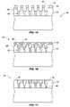
- FIGS. 12 through 14are scanning electron micrographs depicting a substrate 10 with recesses 18 L, 18 H that have been formed at two different elevations L and H by forming a nonconformal mask of TC/DARC over recess 18 L, creating a pattern in the nonconformal mask, and subsequently transferring the pattern into substrate 10 .
- FIG. 12is a perspective view of substrate 10 .
- FIG. 13is a side view, with higher elevation H features on the left and in the background behind the lower elevation L features that appear on the right.
- lower elevation L features of substrate 10are in the foreground and higher elevation H features are in the background.
- the micrographs of FIGS. 12 through 14demonstrate that when embodiments of the present invention are employed, feature dimensions and, thus, critical dimensions, remain undistorted or substantially undistorted regardless of the topography of the upper surface 16 ( FIG. 1 ) of a substrate 10 over which a mask is formed.
- a mask 30 according to embodiments of the present inventionmay be useful for fabricating a variety of structures, including structures that have conventionally been fabricated using two or more sequential mask-and-removal processes, as well as structures that include relatively deep trenches or other recesses.
- Various embodiments of structures that may be fabricated in accordance with embodiments of the present inventioninclude, but are not limited to, PSOI structures, epi-diodes for phase change random access memory (PCRAM) devices, cross-hair cell (CHC) type memory devices, NAND flash memory devices, and other high-voltage devices.
- Embodiments of the present inventionmay also be used to fabricate structures in back-end-of-line (BEOL) processing of semiconductor devices.
- BEOLback-end-of-line
- a specific embodiment of use of the process depicted by FIGS. 1 through 7 in BEOL processingincludes the fabrication of dual damascene copper structures.
- a first pattern 19 of recesses 18 that comprise via holesare formed in the upper surface 16 of a dielectric 14 ′′ ( FIG. 15 ) (e.g., an oxide, such as borophosphosilicate glass (BPSG), etc.) of a substrate 10 .
- a mask 30is then formed over upper surface 16 in accordance with an embodiment of the process described in reference to FIGS. 2 through 6 .
- one or both of a density of vias and a height-aspect ratio of each viamay be increased relative to the maximum useful density and/or height-aspect ratio when conventional processes are used.
- the non-conformal film 20 from which mask 30 is formedmay have a planar or substantially planar upper surface 22 and, in some embodiments, may bridge recesses 18 .
- dielectric 14 ′′may be removed (e.g., by known etch processes, etc.) from dielectric 14 ′′ at upper surface 16 of substrate 10 , through apertures 32 of mask 30 , to define a second pattern 39 ′′ of elongate trenches 38 ′′ in dielectric 14 ′′, which communicate with recesses 18 of first pattern 19 .
- Elongate trenches 38 ′′may be configured to carry conductive lines that communicate with conductive vias that are to be carried by recesses 18 .
- Any conductive material 60 that remains on upper surface 16 of dielectric 14 ′′may then be removed from upper surface 16 to electrically isolate adjacent conductive lines 64 from one another, as shown in FIG. 17 .
- Known processessuch as chemical-mechanical polishing (CMP) or etching, may be used to remove conductive material 60 from upper surface 16 .
Landscapes
- Engineering & Computer Science (AREA)
- Physics & Mathematics (AREA)
- Condensed Matter Physics & Semiconductors (AREA)
- General Physics & Mathematics (AREA)
- Manufacturing & Machinery (AREA)
- Computer Hardware Design (AREA)
- Microelectronics & Electronic Packaging (AREA)
- Power Engineering (AREA)
- Chemical & Material Sciences (AREA)
- Inorganic Chemistry (AREA)
- Drying Of Semiconductors (AREA)
Abstract
Description
- In various embodiments, the present invention relates generally to non-conformal masks. In more specific embodiments, the present invention relates to masks with substantially planar upper surfaces. In some embodiments, a non-conformal mask may bridge recesses in underlying semiconductor device structures. The substantially planarity of the upper surfaces of such masks enables the precise and accurate transfer of patterns from the masks into one or more material layers of the semiconductor device structures.
- Advances in semiconductor device technologies have included the development of a number of complex, intricate structures. Examples of such structures include cross-hair cells, which may be used in dynamic random access memory (DRAM) devices, the epi-diodes of phase-change random access memory (PCRAM) devices, and pseudo silicon-on-insulator (SOI) structures. Fabrication of these and other structures typically requires the use of two or more masks, through which material is removed to define the desired structure or structures.
- Once material has been removed through a first mask, the upper, or “active,” surface of the substrate typically includes a number of recesses. As a consequence of the presence of these recesses, one of two undesirable results will occur when conventional conformal mask fabrication processes are used to form a subsequent mask: (1) the recesses must be filled with a sacrificial material before the layer of mask material is applied and the subsequent mask is formed therefrom; or (2) a layer of mask material, such as a photoresist, that will be used to define the subsequent mask will conform to the topography of the semiconductor device structure. When the recesses are not filled before mask material is applied, mask material enters the recesses, resulting in a layer of mask material with a nonplanar surface. The degree of nonplanarity corresponds to the size and/or density of recesses, with the nonplanarity being more pronounced when a substrate includes larger and/or more densely arranged recesses.
- When a conformal mask is formed, different regions of the layer of mask material are located at different elevations. When a layer of photoresist is applied to the layer of mask material, it too will have different regions that are located at different elevations. Unfortunately, the tools that are used to expose the photoresist have a narrow focal plane, which may not coincide with all areas of the photoresist, causing some areas to be exposed to a blurred radiation pattern. When the exposing radiation is blurred, the precision with which mask features (e.g., solid edges, apertures, etc.) may be formed through the photoresist is reduced, as is the precision with which these features may be transferred into the mask material from which the subsequent mask will be defined.
- When the recesses are filled before the mask material is applied, the semiconductor device structure must be subjected to a number of additional processes, including material deposition, planarization, and material removal processes, all of which undesirably add to the overall cost of fabrication, as well as increase the probability that the resulting semiconductor devices will be damaged.
- In the drawings:
FIGS. 1 through 6 are cross-sectional representations of an embodiment of a process for forming a non-conformal mask over a substrate;FIG. 3A is a scanning electron micrograph of an embodiment of a structure that includes a substrate with a non-conformal film of mask material on its upper surface, with the non-conformal film bridging recesses in the upper surface of the substrate;FIG. 7 is a cross-sectional representation showing an embodiment of a process for removing material through an embodiment of a mask of the present invention;FIG. 8 is a scanning electron micrograph of an embodiment of a structure that has been fabricated by employing embodiments of the present invention;FIGS. 9 through 11 are cross-sectional representations that illustrate an embodiment of a pitch multiplication process that uses an embodiment of a non-conformal mask of the present invention;FIGS. 12 through 14 are scanning electron micrographs depicting an embodiment of a multi-elevation structure fabricated using embodiments of the present invention; andFIGS. 15 through 17 depict an embodiment of back end of line processing that employs various embodiments of mask fabrication and material patterning process of the present invention.FIGS. 1 through 7 illustrate an embodiment of a method for fabricating a mask30 (FIG. 6 ) over asubstrate 10. As shown inFIG. 1 ,substrate 10 comprises asemiconductor substrate 12, such as a full or partial wafer of semiconductor material (e.g., silicon, gallium arsenide, indium phosphide, etc.) or a so-called silicon-on-insulator (SOI) type substrate (e.g., silicon-on-ceramic (SOC), silicon-on-diamond (SOD), silicon-on-glass (SOG), silicon-on-sapphire (SOS), etc.).- In some embodiments, a
semiconductor substrate 12 upon which a mask is to be fabricated carries one ormore materials 14 on itsupper surface 13. In the depicted embodiment,recesses 18 extend into anupper surface 16 ofsubstrate 10; i.e., into an upper surface of anuppermost material 14. In some embodiments,recesses 18 define semiconductor device features14′ from one ormore materials 14. In more specific embodiments,recesses 18 may be part of afirst pattern 19 that has been defined insubstrate 10 or frommaterials 14. - As shown in
FIG. 2 , anon-conformal film 20 is formed onupper surface 16. Non-conformalfilm 20 may comprise a material that will serve as a mask30 (FIG. 6 ) for subsequently patterning one ormore materials 14 or other semiconductor device features14′. In some embodiments, non-conformalfilm 20 may comprise a carbon-based material. In more specific embodiments, non-conformalfilm 20 may comprise a so-called “transparent carbon” (TC) or an amorphous carbon. In other embodiments, another suitable mask material, such as a silicon nitride that has been doped with hydrogen, may be used to formnon-conformal film 20. - Non-conformal
film 20 may be formed by processes that impart it with anupper surface 22 that is, at least, more planar than theupper surface 16 over which non-conformalfilm 20 has been formed. In some embodiments,upper surface 22 ofnon-conformal film 20 may be substantially planar or even planar. The planarity or substantial planarity ofupper surface 22 may be achieved solely by way of the process by which non-conformalfilm 20 is formed, without any further processing (e.g., planarization, polishing, etching, etc.) ofupper surface 22. In a specific embodiment, anon-conformal film 20 with anupper surface 22 that is substantially planar may result from embodiments of processes where transparent carbon is deposited by low temperature plasma-enhanced chemical vapor deposition (PECVD) processes. Other processes may, of course, also be used to form anon-conformal film 20 with a substantially planar surface, including processes for formingnon-conformal film 20 from materials other than transparent carbon. - Some embodiments of processes that are used to form
non-conformal film 20 may result in a structure that “bridges” one ormore recesses 18, covering an opening19 of each coveredrecess 18 without completely lining, or substantially entering, that coveredrecess 18. In such embodiments, the processes that are used to formnon-conformal film 20 and the material from whichnon-conformal film 20 is formed are considered in conjunction with the lateral dimensions (e.g., distance across, diameter, etc.) ofrecesses 18, and tailored to minimize or prevent sagging of portions ofnon-conformal film 20 that bridge recesses18 and to impartnon-conformal film 20 with a planar or substantially planarupper surface 22. In embodiments where non-conformalfilm 20 is formed from transparent carbon, the transparent carbon may be deposited by known low temperature PECVD processes. In even more specific embodiments, PECVD may be used to deposit transparent carbon in such a way that it will bridgerecesses 18 that are about 70 nm wide, about 100 nm wide, or even about 120 nm wide, and that are spaced about the same distance apart from one another (i.e., have about the same pitch). Of course, other embodiments of processes for forming anon-conformal film 20 that will bridgerecesses 18 without substantially entering into therecesses 18, including processes for formingnon-conformal film 20 from materials other than transparent carbon, are also within the scope of the present invention. - In some embodiments, a dielectric anti-reflective coating (DARC)
film 24 of a known type may be formed onupper surface 22 ofnon-conformal film 20, as illustrated byFIG. 3 . A DARCfilm 24 is particularly useful in embodiments where photo processes will subsequently be used to form a mask28 (FIG. 5 ) overnon-conformal film 20. DARCfilm 24 may be formed from any suitable material by any suitable process known in the art. In a specific embodiment, DARCfilm 24 may comprise a silicon oxynitride (SiON) film with a stoichiometry that is tailored to minimize reflectance during subsequent photo processing. As DARCfilm 24 is formed on a planar or substantially planarupper surface 22 ofnon-conformal film 20, an upper surface of DARCfilm 24 may also be planar or substantially planar. FIG. 3A is an electron micrograph of a specific embodiment of a structure that may be fabricated using the foregoing techniques. In that structure,substrate 10′ includesrecesses 18′ with undercut regions that are used to isolate adjacent columns of “pseudo silicon-on-insulator” (“PSOI”)structures 60 from one another. A non-conformaltransparent carbon film 20′ having a thickness of about 2,000 Å has been formed over anupper surface 16′ ofsubstrate 10,′ andbridges openings 18Oofrecesses 18′ inupper surface 16′. A DARCfilm 24′ with a thickness of about 320 Å resides upon a substantially planarupper surface 22′ oftransparent carbon film 20′.- Once
non-conformal film 20 and DARCfilm 24, if any, have been formed, a “soft”mask material 26 may be applied to or overupper surface 22 ofnon-conformal film 20, as depicted byFIG. 4 . In embodiments that lack a DARCfilm 24,mask material 26 may be formed directly onupper surface 22 ofnon-conformal film 20. In embodiments where a DARCfilm 24 resides uponupper surface 22 ofnon-conformal film 20,mask material 26 may be formed onupper surface 25 of DARCfilm 24. Various embodiments of mask materials that may be used to formmask material 26 include, without limitation, uncured photoresists, thermoplastic materials, metals, or any other suitable materials. - As depicted by
FIG. 5 , amask 28 may be defined frommask material 26 by patterning the mask material26 (FIG. 4 ). Sincemask material 26 is formed over a planar or substantially planarupper surface FIG. 4 ) ofmask material 26 that is to be patterned, or an area ofmask material 26 in which patterning (e.g., apertures, etc.) ofmask 28 is to be located, may itself be planar or substantially planar, or have a thickness that is uniform or substantially uniform. Thus, distortion ofmask 28 may be minimized or eliminated, providing optimal control over the critical dimensions (CDs) ofmask 28 and of any subsequently formed mask. - In some embodiments, where mask material26 (
FIG. 4 ) comprises uncured photoresist, conventional photolithography processes may be used to expose and develop themask material 26, withmask 28 being the result of such processes. In embodiments where conventional photolithography processes are used to formmask 28 frommask material 26, the planarity or substantial planarity ofmask material 26 or its uniformity or substantial uniformity in thickness may enable a depth of focus (DOF) of radiation emitted by a lithography tool to coincide withmask material 26 across the entirety ofregion 27. - In other embodiments, the planar or substantially planar upper surface27U(
FIG. 4 ) ofregion 27 enables the use of so-called nanoimprint lithography techniques to formmask 28 from mask material26 (FIG. 4 ). Specifically, due to the planarity or substantial planarity ofupper surface 27U, all of the imprint regions of a nanoimprint mold (not shown) may come into simultaneous or substantially simultaneous contact with the entire planar or substantially planarupper surface 27U. The uniform or substantially uniform thickness ofregion 27 enables all areas of the nanoimprint mold to affect all areas ofregion 27 in a uniform or substantially uniform manner, resulting in a distortion-free or substantially distortion-free mask 28. - Appropriate nanoimprint lithography techniques may be effected in a manner known in the art to define
mask 28 frommask material 26. In more specific embodiments, known photo nanoimprint lithography techniques may be used to form amask 28 from amask material 26 that comprises an uncured photoresist, known thermoplastic nanoimprint lithography techniques may be used to form amask 28 from amask material 26 that comprises a thermoplastic material, known electrochemical nanoimprint lithography techniques may be used to form amask 28 from amask material 26 that comprises a metal, and guided self-assembly processes may be used to form amask 28 from monolayers ofappropriate mask materials 26. - The
masks 28 that result from these or other suitable processes may be used in conjunction with a suitable material removal process, as shown inFIG. 6 , to define amask 30 fromnon-conformal film 20. In embodiments wherenon-conformal film 20 comprises transparent carbon, known etching processes may be used to remove material fromnon-conformal film 20 and, thus, to define a pattern therefrom, resulting inmask 30. Mask 30 may, in some embodiments, lack distortion, other than minimal distortion that may occur as an artifact of the process used to form mask28 (FIGS. 4 and 5 ). In embodiments wheremask 28 is formed by photolithography techniques, minimal distortion may be present at locations ofmask 30 that correspond to peripheral regions ofmask 28, which, in turn, correspond to the outer periphery of the field of exposure of a reticle, or photomask, through which radiation is directed to formmask 28.- In other embodiments,
mask 30 may substantially lack distortion. Stated another way, distortion inmask 30 may be limited to minimal distortion, such as that resulting from the process by which mask28 is formed, and nonplanarities that may occur in one or both ofmask material 26 andnon-conformal film 20. FIG. 6 shows an embodiment of astructure 100 in which amask 30 overliesupper surface 16 ofsubstrate 10, as well asrecesses 18 withinupper surface 16. At some locations,apertures 32 ofmask 30 overlap and communicate withrecesses 18. In the depicted embodiment, recesses18 comprise parts of a first pattern19 (FIG. 1 ) that has already been formed inupper surface 16 ofsubstrate 10, whilemask 30 includesapertures 32 that overlap, or “cross,” recesses18 offirst pattern 19 at some locations.- As depicted by
FIG. 7 , such an embodiment of mask30 (FIG. 6 ) may be used with known material removal processes (e.g., etch processes, etc.) to form asecond pattern 39 orrecesses 38 inupper surface 16, withsecond pattern 39 “crossing” and communicating withrecesses 18 offirst pattern 19. - In some embodiments, material of
substrate 10 may be removed throughmask 30 to directlypattern substrate 10, as depicted byFIG. 7 . Conventional material removal processes (e.g., etch processes, etc.) may be used to remove material ofsubstrate 10 throughmask 30. A specific embodiment of a result of a process in which material ofsubstrate 10 is removed throughmask 30, as depicted byFIG. 7 , is shown inFIG. 8 . InFIG. 8 , which is a scanning electron micrograph of an array of PSOI structures60 (incomplete portions of which are illustrated byFIG. 3A ), afirst pattern 19′ comprisesrecesses 18′ for shallow trench isolation (STI) structures that will electrically isolate columns (in the depicted orientation) ofPSOI structures 60 from one another, while asecond pattern 39′ comprisesrecesses 38′ that separate each column into a plurality ofdiscrete PSOI structures 60 that are electrically isolated from one another. - In other embodiments, such as that shown in
FIGS. 9 through 11 ,mask 30 may comprise an intermediate mask for use in pitch multiplication (e.g., pitch doubling, etc.) processes. In one such embodiment, illustrated byFIG. 9 , known processes may be used to form aconformal layer 40 of another mask material overmask 30 and portions ofupper surface 16 that are exposed throughmask 30.Conformal layer 40 may be formed from a material that will withstand processes that remove the material ofmask 30. As depicted byFIG. 10 , regions ofconformal layer 40 that overliemask 30 may be removed. In some embodiments, known etch techniques (e.g., anisotropic etch processes, etc.) may be used to remove these portions ofconformal layer 40, forming a reduced-pitch mask 50 through whichupper surfaces 32 ofmask 30 are exposed. Thereafter, the material ofmask 30 may be removed through, and with selectivity over, the material of reduced-pitch mask 50, as shown inFIG. 11 . Reduced-pitch mask 50 may then be used, in conventional material removal processes (e.g., etch processes, etc.) topattern substrate 10, as known in the art. - Like
mask 30, reduced-pitch mask 50 may includeapertures 52 that overlap, or “cross,” and communicate withrecesses 18 inupper surface 16 ofsubstrate 10. Thus, in some embodiments, reduced-pitch mask 50 may be used to define asecond pattern 39 inupper surface 16 that crosses a previously definedfirst pattern 19 inupper surface 16. FIGS. 12 through 14 are scanning electron micrographs depicting asubstrate 10 withrecesses recess 18L, creating a pattern in the nonconformal mask, and subsequently transferring the pattern intosubstrate 10.FIG. 12 is a perspective view ofsubstrate 10.FIG. 13 is a side view, with higher elevation H features on the left and in the background behind the lower elevation L features that appear on the right. InFIG. 14 , lower elevation L features ofsubstrate 10 are in the foreground and higher elevation H features are in the background. The micrographs ofFIGS. 12 through 14 demonstrate that when embodiments of the present invention are employed, feature dimensions and, thus, critical dimensions, remain undistorted or substantially undistorted regardless of the topography of the upper surface16 (FIG. 1 ) of asubstrate 10 over which a mask is formed.- A
mask 30 according to embodiments of the present invention may be useful for fabricating a variety of structures, including structures that have conventionally been fabricated using two or more sequential mask-and-removal processes, as well as structures that include relatively deep trenches or other recesses. Various embodiments of structures that may be fabricated in accordance with embodiments of the present invention include, but are not limited to, PSOI structures, epi-diodes for phase change random access memory (PCRAM) devices, cross-hair cell (CHC) type memory devices, NAND flash memory devices, and other high-voltage devices. Embodiments of the present invention may also be used to fabricate structures in back-end-of-line (BEOL) processing of semiconductor devices. - A specific embodiment of use of the process depicted by
FIGS. 1 through 7 in BEOL processing includes the fabrication of dual damascene copper structures. Initially, with returned reference toFIG. 1 , afirst pattern 19 ofrecesses 18 that comprise via holes are formed in theupper surface 16 of a dielectric14″ (FIG. 15 ) (e.g., an oxide, such as borophosphosilicate glass (BPSG), etc.) of asubstrate 10. Amask 30 is then formed overupper surface 16 in accordance with an embodiment of the process described in reference toFIGS. 2 through 6 . In embodiments where such processes are used, one or both of a density of vias and a height-aspect ratio of each via may be increased relative to the maximum useful density and/or height-aspect ratio when conventional processes are used. As shown inFIG. 2 , thenon-conformal film 20 from which mask30 is formed may have a planar or substantially planarupper surface 22 and, in some embodiments, may bridge recesses18. - Once
mask 30 has been formed, as shown inFIG. 15 , additional material may be removed (e.g., by known etch processes, etc.) from dielectric14″ atupper surface 16 ofsubstrate 10, throughapertures 32 ofmask 30, to define asecond pattern 39″ ofelongate trenches 38″ in dielectric14″, which communicate withrecesses 18 offirst pattern 19.Elongate trenches 38″ may be configured to carry conductive lines that communicate with conductive vias that are to be carried byrecesses 18. - Thereafter, as shown in
FIG. 16 , recesses18 offirst pattern 19 and recesses38″ ofsecond pattern 39″ may concurrently be filled (e.g., by known material deposition processes, etc.) withconductive material 60 to formconductive vias 62 withinrecesses 18 andconductive lines 64 withinrecesses 38. In a specific embodiment,conductive material 60 may comprise copper, although other conductive materials could also be used. - Any
conductive material 60 that remains onupper surface 16 ofdielectric 14″ may then be removed fromupper surface 16 to electrically isolate adjacentconductive lines 64 from one another, as shown inFIG. 17 . Known processes, such as chemical-mechanical polishing (CMP) or etching, may be used to removeconductive material 60 fromupper surface 16. - Although the foregoing description contains many specifics, these should not be construed as limiting the scope of the present invention, but merely as providing illustrations of some embodiments. Similarly, other embodiments that are within the scope of the invention may also be devised. Features from different embodiments may be employed in combination. The scope of the invention is, therefore, indicated and limited only by the appended claims and their legal equivalents, rather than by the foregoing description. All additions, deletions and modifications to the invention as disclosed herein which fall within the meaning and scope of the claims are to be embraced thereby.
Claims (21)
Priority Applications (2)
| Application Number | Priority Date | Filing Date | Title |
|---|---|---|---|
| US12/477,551US8268730B2 (en) | 2009-06-03 | 2009-06-03 | Methods of masking semiconductor device structures |
| US13/567,741US20120319247A1 (en) | 2009-06-03 | 2012-08-06 | Semiconductor device structures including a mask material |
Applications Claiming Priority (1)
| Application Number | Priority Date | Filing Date | Title |
|---|---|---|---|
| US12/477,551US8268730B2 (en) | 2009-06-03 | 2009-06-03 | Methods of masking semiconductor device structures |
Related Child Applications (1)
| Application Number | Title | Priority Date | Filing Date |
|---|---|---|---|
| US13/567,741DivisionUS20120319247A1 (en) | 2009-06-03 | 2012-08-06 | Semiconductor device structures including a mask material |
Publications (2)
| Publication Number | Publication Date |
|---|---|
| US20100308438A1true US20100308438A1 (en) | 2010-12-09 |
| US8268730B2 US8268730B2 (en) | 2012-09-18 |
Family
ID=43300143
Family Applications (2)
| Application Number | Title | Priority Date | Filing Date |
|---|---|---|---|
| US12/477,551Active2030-02-20US8268730B2 (en) | 2009-06-03 | 2009-06-03 | Methods of masking semiconductor device structures |
| US13/567,741AbandonedUS20120319247A1 (en) | 2009-06-03 | 2012-08-06 | Semiconductor device structures including a mask material |
Family Applications After (1)
| Application Number | Title | Priority Date | Filing Date |
|---|---|---|---|
| US13/567,741AbandonedUS20120319247A1 (en) | 2009-06-03 | 2012-08-06 | Semiconductor device structures including a mask material |
Country Status (1)
| Country | Link |
|---|---|
| US (2) | US8268730B2 (en) |
Citations (16)
| Publication number | Priority date | Publication date | Assignee | Title |
|---|---|---|---|---|
| US5119127A (en)* | 1989-03-29 | 1992-06-02 | Orc Manufacturing Co., Ltd. | Photoresist exposure method and apparatus therefor |
| US5789306A (en)* | 1996-04-18 | 1998-08-04 | Micron Technology, Inc. | Dual-masked field isolation |
| US5883006A (en)* | 1997-12-12 | 1999-03-16 | Kabushiki Kaisha Toshiba | Method for making a semiconductor device using a flowable oxide film |
| US6303275B1 (en)* | 2000-02-10 | 2001-10-16 | International Business Machines Corporation | Method for resist filling and planarization of high aspect ratio features |
| US6440638B2 (en)* | 1998-09-28 | 2002-08-27 | International Business Machines Corp. | Method and apparatus for resist planarization |
| US6440644B1 (en)* | 1997-10-15 | 2002-08-27 | Kabushiki Kaisha Toshiba | Planarization method and system using variable exposure |
| US6607984B1 (en)* | 2000-06-20 | 2003-08-19 | International Business Machines Corporation | Removable inorganic anti-reflection coating process |
| US7071072B2 (en)* | 2004-06-11 | 2006-07-04 | International Business Machines Corporation | Forming shallow trench isolation without the use of CMP |
| US20060211260A1 (en)* | 2005-03-15 | 2006-09-21 | Luan Tran | Pitch reduced patterns relative to photolithography features |
| US20070049011A1 (en)* | 2005-09-01 | 2007-03-01 | Micron Technology, Inc., A Corporation | Method of forming isolated features using pitch multiplication |
| US20070238299A1 (en)* | 2006-04-07 | 2007-10-11 | Micron Technology, Inc. | Simplified pitch doubling process flow |
| US20070259457A1 (en)* | 2006-05-04 | 2007-11-08 | Texas Instruments | Optical endpoint detection of planarization |
| US20080085612A1 (en)* | 2006-10-05 | 2008-04-10 | Micron Technology, Inc. | Method to deposit conformal low temperature SiO2 |
| US20100041204A1 (en)* | 2008-08-13 | 2010-02-18 | Mark Kiehlbauch | Methods Of Making Capacitors, DRAM Arrays and Electronic Systems |
| US7842558B2 (en)* | 2006-03-02 | 2010-11-30 | Micron Technology, Inc. | Masking process for simultaneously patterning separate regions |
| US7911728B2 (en)* | 2008-11-26 | 2011-03-22 | Hitachi Global Storage Technologies Netherlands B.V. | Method for servowriting a patterned-media perpendicular magnetic recording disk using position error signal (PES) alignment fields |
Family Cites Families (6)
| Publication number | Priority date | Publication date | Assignee | Title |
|---|---|---|---|---|
| US6493926B2 (en)* | 2001-04-16 | 2002-12-17 | Headway Technologies, Inc. | Bi-layer lift-off process for high track density GMR head |
| DE102005023059A1 (en)* | 2005-05-19 | 2006-11-23 | Austriamicrosystems Ag | Method for producing a micromechanical structural element and semiconductor device |
| JP4462249B2 (en)* | 2005-09-22 | 2010-05-12 | ソニー株式会社 | Light emitting diode manufacturing method, integrated light emitting diode manufacturing method, and nitride III-V compound semiconductor growth method |
| DE102006042617B4 (en)* | 2006-09-05 | 2010-04-08 | Q-Cells Se | Method for generating local contacts |
| KR100946080B1 (en)* | 2007-12-28 | 2010-03-10 | 주식회사 하이닉스반도체 | Pattern formation method of semiconductor device |
| US20090323411A1 (en)* | 2008-06-30 | 2009-12-31 | Qimonda Ag | Method including selective treatment of storage layer |
- 2009
- 2009-06-03USUS12/477,551patent/US8268730B2/enactiveActive
- 2012
- 2012-08-06USUS13/567,741patent/US20120319247A1/ennot_activeAbandoned
Patent Citations (16)
| Publication number | Priority date | Publication date | Assignee | Title |
|---|---|---|---|---|
| US5119127A (en)* | 1989-03-29 | 1992-06-02 | Orc Manufacturing Co., Ltd. | Photoresist exposure method and apparatus therefor |
| US5789306A (en)* | 1996-04-18 | 1998-08-04 | Micron Technology, Inc. | Dual-masked field isolation |
| US6440644B1 (en)* | 1997-10-15 | 2002-08-27 | Kabushiki Kaisha Toshiba | Planarization method and system using variable exposure |
| US5883006A (en)* | 1997-12-12 | 1999-03-16 | Kabushiki Kaisha Toshiba | Method for making a semiconductor device using a flowable oxide film |
| US6440638B2 (en)* | 1998-09-28 | 2002-08-27 | International Business Machines Corp. | Method and apparatus for resist planarization |
| US6303275B1 (en)* | 2000-02-10 | 2001-10-16 | International Business Machines Corporation | Method for resist filling and planarization of high aspect ratio features |
| US6607984B1 (en)* | 2000-06-20 | 2003-08-19 | International Business Machines Corporation | Removable inorganic anti-reflection coating process |
| US7071072B2 (en)* | 2004-06-11 | 2006-07-04 | International Business Machines Corporation | Forming shallow trench isolation without the use of CMP |
| US20060211260A1 (en)* | 2005-03-15 | 2006-09-21 | Luan Tran | Pitch reduced patterns relative to photolithography features |
| US20070049011A1 (en)* | 2005-09-01 | 2007-03-01 | Micron Technology, Inc., A Corporation | Method of forming isolated features using pitch multiplication |
| US7842558B2 (en)* | 2006-03-02 | 2010-11-30 | Micron Technology, Inc. | Masking process for simultaneously patterning separate regions |
| US20070238299A1 (en)* | 2006-04-07 | 2007-10-11 | Micron Technology, Inc. | Simplified pitch doubling process flow |
| US20070259457A1 (en)* | 2006-05-04 | 2007-11-08 | Texas Instruments | Optical endpoint detection of planarization |
| US20080085612A1 (en)* | 2006-10-05 | 2008-04-10 | Micron Technology, Inc. | Method to deposit conformal low temperature SiO2 |
| US20100041204A1 (en)* | 2008-08-13 | 2010-02-18 | Mark Kiehlbauch | Methods Of Making Capacitors, DRAM Arrays and Electronic Systems |
| US7911728B2 (en)* | 2008-11-26 | 2011-03-22 | Hitachi Global Storage Technologies Netherlands B.V. | Method for servowriting a patterned-media perpendicular magnetic recording disk using position error signal (PES) alignment fields |
Also Published As
| Publication number | Publication date |
|---|---|
| US8268730B2 (en) | 2012-09-18 |
| US20120319247A1 (en) | 2012-12-20 |
Similar Documents
| Publication | Publication Date | Title |
|---|---|---|
| US7531456B2 (en) | Method of forming self-aligned double pattern | |
| US9911646B2 (en) | Self-aligned double spacer patterning process | |
| US9831117B2 (en) | Self-aligned double spacer patterning process | |
| CN104136994B (en) | Dual hard mask photoetching process | |
| JP5244793B2 (en) | Nanoimprint technology with improved flexibility for alignment and feature shaping | |
| US9437447B2 (en) | Method for patterning a substrate for planarization | |
| US6645851B1 (en) | Method of forming planarized coatings on contact hole patterns of various duty ratios | |
| US20080076070A1 (en) | Methods of Forming Fine Patterns In Integrated Circuits Using Atomic Layer Deposition | |
| US20170148637A1 (en) | Methods of Forming Etch Masks for Sub-Resolution Substrate Patterning | |
| US10312088B1 (en) | Self-aligned double patterning method | |
| US10734284B2 (en) | Method of self-aligned double patterning | |
| US20070128823A1 (en) | Method of fabricating semiconductor integrated circuit device | |
| KR102752996B1 (en) | Methods for planarization of spin-on and CVD deposited organic films | |
| TWI358789B (en) | Method for dual damascene process | |
| US8268730B2 (en) | Methods of masking semiconductor device structures | |
| US7268080B2 (en) | Method for printing contacts on a substrate | |
| KR100843948B1 (en) | Method of forming fine pattern of semiconductor device | |
| US8119523B2 (en) | Method for fabricating semiconductor device using dual damascene process | |
| US20250167001A1 (en) | Patterning processes utilizing directional deposition | |
| CN112670168B (en) | Method for forming semiconductor structure and transistor | |
| KR100912958B1 (en) | Manufacturing method of fine pattern of semiconductor device | |
| US10916427B2 (en) | Forming contact holes using litho-etch-litho-etch approach | |
| KR101103809B1 (en) | Manufacturing Method of Semiconductor Device | |
| KR20110001718A (en) | Method for forming semiconductor device | |
| KR20110030924A (en) | Micro pattern formation method using double patterning process |
Legal Events
| Date | Code | Title | Description |
|---|---|---|---|
| AS | Assignment | Owner name:MICRON TECHNOLOGY, INC., IDAHO Free format text:ASSIGNMENT OF ASSIGNORS INTEREST;ASSIGNOR:WELLS, DAVID H.;REEL/FRAME:022775/0120 Effective date:20090601 | |
| FEPP | Fee payment procedure | Free format text:PAYOR NUMBER ASSIGNED (ORIGINAL EVENT CODE: ASPN); ENTITY STATUS OF PATENT OWNER: LARGE ENTITY | |
| STCF | Information on status: patent grant | Free format text:PATENTED CASE | |
| CC | Certificate of correction | ||
| FPAY | Fee payment | Year of fee payment:4 | |
| AS | Assignment | Owner name:U.S. BANK NATIONAL ASSOCIATION, AS COLLATERAL AGENT, CALIFORNIA Free format text:SECURITY INTEREST;ASSIGNOR:MICRON TECHNOLOGY, INC.;REEL/FRAME:038669/0001 Effective date:20160426 Owner name:U.S. BANK NATIONAL ASSOCIATION, AS COLLATERAL AGEN Free format text:SECURITY INTEREST;ASSIGNOR:MICRON TECHNOLOGY, INC.;REEL/FRAME:038669/0001 Effective date:20160426 | |
| AS | Assignment | Owner name:MORGAN STANLEY SENIOR FUNDING, INC., AS COLLATERAL AGENT, MARYLAND Free format text:PATENT SECURITY AGREEMENT;ASSIGNOR:MICRON TECHNOLOGY, INC.;REEL/FRAME:038954/0001 Effective date:20160426 Owner name:MORGAN STANLEY SENIOR FUNDING, INC., AS COLLATERAL Free format text:PATENT SECURITY AGREEMENT;ASSIGNOR:MICRON TECHNOLOGY, INC.;REEL/FRAME:038954/0001 Effective date:20160426 | |
| AS | Assignment | Owner name:U.S. BANK NATIONAL ASSOCIATION, AS COLLATERAL AGENT, CALIFORNIA Free format text:CORRECTIVE ASSIGNMENT TO CORRECT THE REPLACE ERRONEOUSLY FILED PATENT #7358718 WITH THE CORRECT PATENT #7358178 PREVIOUSLY RECORDED ON REEL 038669 FRAME 0001. ASSIGNOR(S) HEREBY CONFIRMS THE SECURITY INTEREST;ASSIGNOR:MICRON TECHNOLOGY, INC.;REEL/FRAME:043079/0001 Effective date:20160426 Owner name:U.S. BANK NATIONAL ASSOCIATION, AS COLLATERAL AGEN Free format text:CORRECTIVE ASSIGNMENT TO CORRECT THE REPLACE ERRONEOUSLY FILED PATENT #7358718 WITH THE CORRECT PATENT #7358178 PREVIOUSLY RECORDED ON REEL 038669 FRAME 0001. ASSIGNOR(S) HEREBY CONFIRMS THE SECURITY INTEREST;ASSIGNOR:MICRON TECHNOLOGY, INC.;REEL/FRAME:043079/0001 Effective date:20160426 | |
| AS | Assignment | Owner name:JPMORGAN CHASE BANK, N.A., AS COLLATERAL AGENT, ILLINOIS Free format text:SECURITY INTEREST;ASSIGNORS:MICRON TECHNOLOGY, INC.;MICRON SEMICONDUCTOR PRODUCTS, INC.;REEL/FRAME:047540/0001 Effective date:20180703 Owner name:JPMORGAN CHASE BANK, N.A., AS COLLATERAL AGENT, IL Free format text:SECURITY INTEREST;ASSIGNORS:MICRON TECHNOLOGY, INC.;MICRON SEMICONDUCTOR PRODUCTS, INC.;REEL/FRAME:047540/0001 Effective date:20180703 | |
| AS | Assignment | Owner name:MICRON TECHNOLOGY, INC., IDAHO Free format text:RELEASE BY SECURED PARTY;ASSIGNOR:U.S. BANK NATIONAL ASSOCIATION, AS COLLATERAL AGENT;REEL/FRAME:047243/0001 Effective date:20180629 | |
| AS | Assignment | Owner name:MICRON TECHNOLOGY, INC., IDAHO Free format text:RELEASE BY SECURED PARTY;ASSIGNOR:MORGAN STANLEY SENIOR FUNDING, INC., AS COLLATERAL AGENT;REEL/FRAME:050937/0001 Effective date:20190731 | |
| AS | Assignment | Owner name:MICRON TECHNOLOGY, INC., IDAHO Free format text:RELEASE BY SECURED PARTY;ASSIGNOR:JPMORGAN CHASE BANK, N.A., AS COLLATERAL AGENT;REEL/FRAME:051028/0001 Effective date:20190731 Owner name:MICRON SEMICONDUCTOR PRODUCTS, INC., IDAHO Free format text:RELEASE BY SECURED PARTY;ASSIGNOR:JPMORGAN CHASE BANK, N.A., AS COLLATERAL AGENT;REEL/FRAME:051028/0001 Effective date:20190731 | |
| MAFP | Maintenance fee payment | Free format text:PAYMENT OF MAINTENANCE FEE, 8TH YEAR, LARGE ENTITY (ORIGINAL EVENT CODE: M1552); ENTITY STATUS OF PATENT OWNER: LARGE ENTITY Year of fee payment:8 | |
| MAFP | Maintenance fee payment | Free format text:PAYMENT OF MAINTENANCE FEE, 12TH YEAR, LARGE ENTITY (ORIGINAL EVENT CODE: M1553); ENTITY STATUS OF PATENT OWNER: LARGE ENTITY Year of fee payment:12 |