US20100307591A1 - Single-Junction Photovoltaic Cell - Google Patents
Single-Junction Photovoltaic CellDownload PDFInfo
- Publication number
- US20100307591A1 US20100307591A1US12/713,572US71357210AUS2010307591A1US 20100307591 A1US20100307591 A1US 20100307591A1US 71357210 AUS71357210 AUS 71357210AUS 2010307591 A1US2010307591 A1US 2010307591A1
- Authority
- US
- United States
- Prior art keywords
- layer
- semiconductor
- forming
- semiconductor substrate
- photovoltaic cell
- Prior art date
- Legal status (The legal status is an assumption and is not a legal conclusion. Google has not performed a legal analysis and makes no representation as to the accuracy of the status listed.)
- Granted
Links
- 239000004065semiconductorSubstances0.000claimsabstractdescription90
- 239000000758substrateSubstances0.000claimsabstractdescription77
- 239000002184metalSubstances0.000claimsabstractdescription40
- 229910052751metalInorganic materials0.000claimsabstractdescription40
- 238000000034methodMethods0.000claimsabstractdescription26
- 239000002019doping agentSubstances0.000claimsabstractdescription19
- JBRZTFJDHDCESZ-UHFFFAOYSA-NAsGaChemical compound[As]#[Ga]JBRZTFJDHDCESZ-UHFFFAOYSA-N0.000claimsdescription12
- 229910001218Gallium arsenideInorganic materials0.000claimsdescription10
- PXHVJJICTQNCMI-UHFFFAOYSA-NNickelChemical compound[Ni]PXHVJJICTQNCMI-UHFFFAOYSA-N0.000claimsdescription8
- 238000002425crystallisationMethods0.000claimsdescription5
- 230000008025crystallizationEffects0.000claimsdescription5
- 239000011521glassSubstances0.000claimsdescription5
- 230000015572biosynthetic processEffects0.000claimsdescription4
- 238000009713electroplatingMethods0.000claimsdescription4
- 239000010936titaniumSubstances0.000claimsdescription4
- 239000011701zincSubstances0.000claimsdescription4
- 239000011888foilSubstances0.000claimsdescription3
- 229920000642polymerPolymers0.000claimsdescription3
- 229910052719titaniumInorganic materials0.000claimsdescription3
- RTAQQCXQSZGOHL-UHFFFAOYSA-NTitaniumChemical compound[Ti]RTAQQCXQSZGOHL-UHFFFAOYSA-N0.000claimsdescription2
- 239000002390adhesive tapeSubstances0.000claimsdescription2
- 239000012528membraneSubstances0.000claimsdescription2
- 229910052759nickelInorganic materials0.000claimsdescription2
- HCHKCACWOHOZIP-UHFFFAOYSA-NZincChemical compound[Zn]HCHKCACWOHOZIP-UHFFFAOYSA-N0.000claims2
- 229910010293ceramic materialInorganic materials0.000claims2
- 239000004020conductorSubstances0.000claims2
- 229910052725zincInorganic materials0.000claims2
- 238000004901spallingMethods0.000description13
- 150000001875compoundsChemical class0.000description9
- 239000000463materialSubstances0.000description6
- 238000007747platingMethods0.000description5
- 238000005229chemical vapour depositionMethods0.000description3
- 230000003287optical effectEffects0.000description3
- 238000005240physical vapour depositionMethods0.000description3
- 230000002269spontaneous effectEffects0.000description3
- 239000002699waste materialSubstances0.000description3
- KDLHZDBZIXYQEI-UHFFFAOYSA-NPalladiumChemical compound[Pd]KDLHZDBZIXYQEI-UHFFFAOYSA-N0.000description2
- 229910045601alloyInorganic materials0.000description2
- 239000000956alloySubstances0.000description2
- 238000009792diffusion processMethods0.000description2
- 238000007654immersionMethods0.000description2
- 238000012986modificationMethods0.000description2
- 230000004048modificationEffects0.000description2
- 238000007650screen-printingMethods0.000description2
- 229910003962NiZnInorganic materials0.000description1
- 229910021586Nickel(II) chlorideInorganic materials0.000description1
- GRYLNZFGIOXLOG-UHFFFAOYSA-NNitric acidChemical compoundO[N+]([O-])=OGRYLNZFGIOXLOG-UHFFFAOYSA-N0.000description1
- 238000010521absorption reactionMethods0.000description1
- QZPSXPBJTPJTSZ-UHFFFAOYSA-Naqua regiaChemical compoundCl.O[N+]([O-])=OQZPSXPBJTPJTSZ-UHFFFAOYSA-N0.000description1
- KGBXLFKZBHKPEV-UHFFFAOYSA-Nboric acidChemical compoundOB(O)OKGBXLFKZBHKPEV-UHFFFAOYSA-N0.000description1
- 239000004327boric acidSubstances0.000description1
- 239000000919ceramicSubstances0.000description1
- 238000000151depositionMethods0.000description1
- 230000008021depositionEffects0.000description1
- 230000000694effectsEffects0.000description1
- 238000007772electroless platingMethods0.000description1
- 238000005530etchingMethods0.000description1
- 238000001459lithographyMethods0.000description1
- 238000004519manufacturing processMethods0.000description1
- 239000007769metal materialSubstances0.000description1
- 239000000203mixtureSubstances0.000description1
- QMMRZOWCJAIUJA-UHFFFAOYSA-Lnickel dichlorideChemical compoundCl[Ni]ClQMMRZOWCJAIUJA-UHFFFAOYSA-L0.000description1
- 229910017604nitric acidInorganic materials0.000description1
- 238000010899nucleationMethods0.000description1
- 229910052763palladiumInorganic materials0.000description1
- 238000000059patterningMethods0.000description1
- 238000001020plasma etchingMethods0.000description1
- 238000012805post-processingMethods0.000description1
- 238000012545processingMethods0.000description1
- 238000001228spectrumMethods0.000description1
- 239000000126substanceSubstances0.000description1
- JBQYATWDVHIOAR-UHFFFAOYSA-NtellanylidenegermaniumChemical compound[Te]=[Ge]JBQYATWDVHIOAR-UHFFFAOYSA-N0.000description1
- XLYOFNOQVPJJNP-UHFFFAOYSA-NwaterSubstancesOXLYOFNOQVPJJNP-UHFFFAOYSA-N0.000description1
Images


Classifications
- H—ELECTRICITY
- H10—SEMICONDUCTOR DEVICES; ELECTRIC SOLID-STATE DEVICES NOT OTHERWISE PROVIDED FOR
- H10F—INORGANIC SEMICONDUCTOR DEVICES SENSITIVE TO INFRARED RADIATION, LIGHT, ELECTROMAGNETIC RADIATION OF SHORTER WAVELENGTH OR CORPUSCULAR RADIATION
- H10F77/00—Constructional details of devices covered by this subclass
- H10F77/10—Semiconductor bodies
- H10F77/12—Active materials
- H10F77/124—Active materials comprising only Group III-V materials, e.g. GaAs
- H10F77/1243—Active materials comprising only Group III-V materials, e.g. GaAs characterised by the dopants
- H—ELECTRICITY
- H10—SEMICONDUCTOR DEVICES; ELECTRIC SOLID-STATE DEVICES NOT OTHERWISE PROVIDED FOR
- H10F—INORGANIC SEMICONDUCTOR DEVICES SENSITIVE TO INFRARED RADIATION, LIGHT, ELECTROMAGNETIC RADIATION OF SHORTER WAVELENGTH OR CORPUSCULAR RADIATION
- H10F77/00—Constructional details of devices covered by this subclass
- H10F77/10—Semiconductor bodies
- H10F77/12—Active materials
- H10F77/124—Active materials comprising only Group III-V materials, e.g. GaAs
- H—ELECTRICITY
- H10—SEMICONDUCTOR DEVICES; ELECTRIC SOLID-STATE DEVICES NOT OTHERWISE PROVIDED FOR
- H10F—INORGANIC SEMICONDUCTOR DEVICES SENSITIVE TO INFRARED RADIATION, LIGHT, ELECTROMAGNETIC RADIATION OF SHORTER WAVELENGTH OR CORPUSCULAR RADIATION
- H10F10/00—Individual photovoltaic cells, e.g. solar cells
- H10F10/10—Individual photovoltaic cells, e.g. solar cells having potential barriers
- H10F10/16—Photovoltaic cells having only PN heterojunction potential barriers
- H10F10/161—Photovoltaic cells having only PN heterojunction potential barriers comprising multiple PN heterojunctions, e.g. tandem cells
- H—ELECTRICITY
- H10—SEMICONDUCTOR DEVICES; ELECTRIC SOLID-STATE DEVICES NOT OTHERWISE PROVIDED FOR
- H10F—INORGANIC SEMICONDUCTOR DEVICES SENSITIVE TO INFRARED RADIATION, LIGHT, ELECTROMAGNETIC RADIATION OF SHORTER WAVELENGTH OR CORPUSCULAR RADIATION
- H10F10/00—Individual photovoltaic cells, e.g. solar cells
- H10F10/10—Individual photovoltaic cells, e.g. solar cells having potential barriers
- H10F10/16—Photovoltaic cells having only PN heterojunction potential barriers
- H10F10/164—Photovoltaic cells having only PN heterojunction potential barriers comprising heterojunctions with Group IV materials, e.g. ITO/Si or GaAs/SiGe photovoltaic cells
- H—ELECTRICITY
- H10—SEMICONDUCTOR DEVICES; ELECTRIC SOLID-STATE DEVICES NOT OTHERWISE PROVIDED FOR
- H10F—INORGANIC SEMICONDUCTOR DEVICES SENSITIVE TO INFRARED RADIATION, LIGHT, ELECTROMAGNETIC RADIATION OF SHORTER WAVELENGTH OR CORPUSCULAR RADIATION
- H10F10/00—Individual photovoltaic cells, e.g. solar cells
- H10F10/10—Individual photovoltaic cells, e.g. solar cells having potential barriers
- H10F10/17—Photovoltaic cells having only PIN junction potential barriers
- H10F10/172—Photovoltaic cells having only PIN junction potential barriers comprising multiple PIN junctions, e.g. tandem cells
- H—ELECTRICITY
- H10—SEMICONDUCTOR DEVICES; ELECTRIC SOLID-STATE DEVICES NOT OTHERWISE PROVIDED FOR
- H10F—INORGANIC SEMICONDUCTOR DEVICES SENSITIVE TO INFRARED RADIATION, LIGHT, ELECTROMAGNETIC RADIATION OF SHORTER WAVELENGTH OR CORPUSCULAR RADIATION
- H10F19/00—Integrated devices, or assemblies of multiple devices, comprising at least one photovoltaic cell covered by group H10F10/00, e.g. photovoltaic modules
- H—ELECTRICITY
- H10—SEMICONDUCTOR DEVICES; ELECTRIC SOLID-STATE DEVICES NOT OTHERWISE PROVIDED FOR
- H10F—INORGANIC SEMICONDUCTOR DEVICES SENSITIVE TO INFRARED RADIATION, LIGHT, ELECTROMAGNETIC RADIATION OF SHORTER WAVELENGTH OR CORPUSCULAR RADIATION
- H10F71/00—Manufacture or treatment of devices covered by this subclass
- H10F71/139—Manufacture or treatment of devices covered by this subclass using temporary substrates
- H10F71/1395—Manufacture or treatment of devices covered by this subclass using temporary substrates for thin-film devices
- H—ELECTRICITY
- H10—SEMICONDUCTOR DEVICES; ELECTRIC SOLID-STATE DEVICES NOT OTHERWISE PROVIDED FOR
- H10F—INORGANIC SEMICONDUCTOR DEVICES SENSITIVE TO INFRARED RADIATION, LIGHT, ELECTROMAGNETIC RADIATION OF SHORTER WAVELENGTH OR CORPUSCULAR RADIATION
- H10F71/00—Manufacture or treatment of devices covered by this subclass
- H10F71/127—The active layers comprising only Group III-V materials, e.g. GaAs or InP
- Y—GENERAL TAGGING OF NEW TECHNOLOGICAL DEVELOPMENTS; GENERAL TAGGING OF CROSS-SECTIONAL TECHNOLOGIES SPANNING OVER SEVERAL SECTIONS OF THE IPC; TECHNICAL SUBJECTS COVERED BY FORMER USPC CROSS-REFERENCE ART COLLECTIONS [XRACs] AND DIGESTS
- Y02—TECHNOLOGIES OR APPLICATIONS FOR MITIGATION OR ADAPTATION AGAINST CLIMATE CHANGE
- Y02E—REDUCTION OF GREENHOUSE GAS [GHG] EMISSIONS, RELATED TO ENERGY GENERATION, TRANSMISSION OR DISTRIBUTION
- Y02E10/00—Energy generation through renewable energy sources
- Y02E10/50—Photovoltaic [PV] energy
- Y02E10/544—Solar cells from Group III-V materials
- Y—GENERAL TAGGING OF NEW TECHNOLOGICAL DEVELOPMENTS; GENERAL TAGGING OF CROSS-SECTIONAL TECHNOLOGIES SPANNING OVER SEVERAL SECTIONS OF THE IPC; TECHNICAL SUBJECTS COVERED BY FORMER USPC CROSS-REFERENCE ART COLLECTIONS [XRACs] AND DIGESTS
- Y02—TECHNOLOGIES OR APPLICATIONS FOR MITIGATION OR ADAPTATION AGAINST CLIMATE CHANGE
- Y02E—REDUCTION OF GREENHOUSE GAS [GHG] EMISSIONS, RELATED TO ENERGY GENERATION, TRANSMISSION OR DISTRIBUTION
- Y02E10/00—Energy generation through renewable energy sources
- Y02E10/50—Photovoltaic [PV] energy
- Y02E10/548—Amorphous silicon PV cells
Definitions
- the present inventionis directed to semiconductor substrate fabrication using stress-induced substrate spalling.
- An example compound semiconductor substrateis gallium arsenide (GaAs), which may be used as the base substrate in high efficiency multi-junction cells.
- GaAsgallium arsenide
- the high optical absorption of GaAsensures that less than about 10 microns of thickness of GaAs is sufficient to capture photons from the solar spectrum; the remaining substrate material serves as a carrier, and is not necessary for the functioning of a PV cell.
- a method for forming a single junction photovoltaic cellincludes forming a dopant layer on a surface of a semiconductor substrate; diffusing the dopant layer into the semiconductor substrate to form a doped layer of the semiconductor substrate; forming a metal layer over the doped layer, wherein a tensile stress in the metal layer is configured to cause a fracture in the semiconductor substrate; removing a semiconductor layer from the semiconductor substrate at the fracture; and forming the single-junction photovoltaic cell using the semiconductor layer.
- a single-junction photovoltaic cellincludes a doped layer comprising a dopant diffused into a semiconductor substrate; a patterned conducting layer formed on the doped layer; a semiconductor layer comprising the semiconductor substrate located on the doped layer on a surface of the doped layer opposite the patterned conducting layer; and an ohmic contact layer formed on the semiconductor layer.
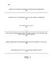
- FIG. 1illustrates an embodiment of a method for forming a single-junction PV cell.
- FIG. 2illustrates an embodiment of a semiconductor substrate with a dopant layer.
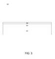
- FIG. 3illustrates an embodiment of a semiconductor substrate with a doped layer.
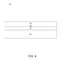
- FIG. 4illustrates an embodiment of a semiconductor substrate with a stressed metal layer.
- FIG. 5illustrates an embodiment of a semiconductor substrate after spalling.
- FIG. 6illustrates an embodiment of a single-junction PV cell.
- Embodiments of systems and methods for forming a single junction PV cellare provided, with exemplary embodiments being discussed below in detail.
- a method for forming relatively thin layer of a compound semiconductor substrate, such as GaAswith relatively little waste of the substrate is needed. Spalling provides for a method of forming a relatively thin semiconductor substrate layer from a larger wafer or ingot of the semiconductor substrate in a cost-effective manner, reducing waste of the substrate material.
- the relatively thin layermay be less than about 50 microns ( ⁇ m) thick in some embodiments, and may be used to form the single junction PV cell.
- Substrate spallinginduces a fracture in a substrate by applying one or more tensile stressed metal layers to the substrate.
- the fracture trajectorymay be unstable, leading to difficult and inconsistent layer removal.
- the use of a ⁇ 110> surface-oriented compound semiconductor substratehas relatively consistent substrate spalling characteristics compared to ⁇ 111> and ⁇ 100> surface crystallization orientations.
- FIG. 1illustrates an embodiment of a method 100 for formation of a single junction PV cell.
- the semiconductor substratemay comprise an n-type or a p-type semiconductor substrate.
- the compound semiconductor substratemay comprise a compound semiconductor substrate, such as GaAs, in some embodiments, and may have a ⁇ 110> surface crystallization orientation in some embodiments.
- FIG. 1is discussed with reference to FIGS. 2-6 .
- a dopant layer 202is formed on semiconductor substrate 201 , as shown in FIG. 2 .
- Dopant layer 202may be formed by any appropriate method, including but not limited to electroplating, CVD, PVD, or screen printing.
- the dopant layer 202may comprise zinc (Zn), or Zn-containing layers in some embodiments.
- dopant layer 202is diffused into semiconductor substrate 201 , resulting in doped layer 301 as shown in FIG. 3 .
- Doped layer 301may have the same doping type (p- or n-type) as the doping type of substrate 201 , or it may be opposite.
- Doped layer 301may comprise a back surface field (BSF) or an electrical contact layer for a single junction PV cell.
- BSFback surface field
- Doped layer 301may also serve as a seed layer in some embodiments.
- an optional seed layer 302may be formed as is shown in FIG.
- the seed layer 302is optional; if the substrate comprises an n-type semiconductor substrate 201 , seed layer 302 may not be present. In some embodiments, the seed layer 302 may be deposited on dopant layer 202 prior to diffusion step 102 ; in other embodiments, the seed layer 302 may be deposited onto doped layer 301 after diffusion step 102 .
- the seed layer 302may comprise one or more metallic layers.
- the seed layer 302may form an ohmic contact to the doped layer 301 , and/or serve as an etch-stop layer (such as titanium (Ti)) to protect underlying layers during removal of the stressed metal layer 401 during post-processing (discussed below with respect to FIG. 6 ).
- an etch-stop layersuch as titanium (Ti)
- a layer of stressed metal 401is formed over doped layer 301 (or optional seed layer 302 in embodiments in which seed layer 302 is present), as shown in FIG. 4 .
- Stressed metal 401may be formed by electroplating, and may comprise nickel (Ni) in some embodiments.
- the atoms comprising the doped layer 301may form an alloy with the stressed metal 401 , for example, NiZn.
- doped layer 301may serve as both a doped layer 301 and as stressed metal 401 (e.g., doped layer 301 may comprise tensile stressed Zn).
- the stressed metal layer 401may be greater than about 2 ⁇ m thick in some embodiments, and between 3 ⁇ m and 10 ⁇ m in some exemplary embodiments. In embodiments in which substrate 201 comprises an n-type semiconductor substrate, stressed metal 401 may be directly electroplated on the surface of substrate 201 , with no need for seeding. The tensile stress contained in stressed metal 401 may be greater than about 100 megapascals (MPa) in some embodiments.
- MPamegapascals
- stressed metal 401 , optional seed layer 302 , doped layer 301 , and semiconductor layer 501are spalled from semiconductor substrate 201 , as shown in FIG. 5 .
- Spallingmay comprise controlled or spontaneous spalling. Controlled spalling may be performed by adhering a flexible handle layer 502 onto stressed metal layer 401 , using flexible handle layer 502 and the tensile stress contained in stressed metal 401 to initiate fracture 503 within substrate 201 , and removing semiconductor layer 501 , optional seed layer 302 , doped semiconductor layer 301 , tensile stressed layer 401 , and flexible handle layer 502 from substrate 201 .
- the handle layer 502may comprise a membrane of plastic, polymer, glass or metal, and may be water soluble in some embodiments. Handle layer 502 may also comprise a specialized adhesive tape that is thermally, optically or chemically-releasable from stressed metal 401 . Alternately, in spontaneous spalling, the tensile stress in stressed metal layer 401 may self-initiate fracture 503 , separating semiconductor layer 501 from substrate 201 without the need for handle layer 502 . Semiconductor layer 501 may be less than about 50 microns thick in some embodiments. Due to the tensile stress in metal layer 401 , the semiconductor layer 501 and doped semiconductor layer 301 may possess residual compressive strain after spalling in some embodiments.
- the magnitude of the strain contained in semiconductor layer 501 and doped semiconductor layer 301may be controlled by varying the thickness and/or stress of the metal layer 401 , either before or after spalling.
- the optical properties of a PV cell built using semiconductor layer 501may be tuned by adjusting the amount of strain in semiconductor layer 501 .
- a single junction PV cell 600is formed using semiconductor layer 501 .
- Contact layer 601is deposited onto the semiconductor layer 501 .
- Contact layer 601may comprise a material appropriate for forming an ohmic contact for semiconductor layer 501 .
- contact layer 601may comprise a GePd or GeAu alloy if semiconductor layer 501 comprises n-type GaAs.
- a handling substrate 602is then formed on contact layer 601 .
- the handling substrate 602may comprise a metallic foil, ceramic, glass or polymer-based material, and may be electrically conducting.
- Handle layer 502 and stressed metal 401are then removed.
- the stressed metal 401may be selectively etched chemically, or may be removed by reactive ion etching.
- a solution of aqua regia(a HNO 3 and HCl mixture) may be used for etching of stressed metal 401 ; in such an embodiment, a seed layer 302 comprising Ti may act as an etch-stop layer to protect doped layer 301 and semiconductor layer 501 .
- Patterned contact layer 603 a - dmay be formed by patterning optional seed layer 302 and/or doped layer 301 using standard lithography to etch any excess metal. Alternately, patterned contact layer 603 a - d may be formed by deposition or screen-printing an appropriate metallic material on the surface of optional seed layer 302 or doped layer 301 after removal of stressed metal 401 .
- Semiconductor layer 501may contain an amount of compressive strain induced in the semiconductor layer 501 by the stress in metal layer 401 ; the amount of strain in semiconductor layer 501 may determine the optical properties of single junction PV cell 600 .
- substrate 201may comprise ⁇ 110> n-type phosphorus-doped GaAs, having a resistance of about 10 Ohm/cm.
- the substrate 201may be an ingot that is about 43 mm in diameter.
- the stressed metal layer 401may be formed by electroplating substrate 201 with Ni using a plating solution comprising 300 g/l NiCl 2 and 20 g/l boric acid at 25° C. for 5 minutes with a plating current of 0.6 Amps.
- the Ni stressed metal layer 401 that is formed on substrate 201may spontaneously initiate fracture (i.e., spontaneous spalling) from the edge of the substrate 201 , separating a semiconductor layer 501 of GaAs from the substrate 201 .
- the semiconductor layer 501 of GaAsmay be about 10 ⁇ m thick, with a Ni layer 401 that is about 5 ⁇ m thick.
- Semiconductor layer 501may be used to form a single junction PV cell 600 .
- the technical effects and benefits of exemplary embodimentsinclude formation of a relatively thin layer of a compound semiconductor substrate for use in a single junction PV cell in a relatively cost-effective manner.
Landscapes
- Photovoltaic Devices (AREA)
- Electrodes Of Semiconductors (AREA)
Abstract
Description
- This application claims the benefit of U.S. Provisional Application No. 61/185,247, filed Jun. 9, 2009. This application is also related to attorney docket numbers YOR920100056US1, YOR920100058US1, YOR920100060US1, and FIS920100005US1, each assigned to International Business Machines Corporation (IBM) and filed on the same day as the instant application, all of which are herein incorporated by reference in their entirety.
- The present invention is directed to semiconductor substrate fabrication using stress-induced substrate spalling.
- Cost constraints tend to exclude the use of compound semiconductor substrates for all but the most demanding photovoltaic (PV) applications, such as satellite and space-based PV systems, as compound semiconductor substrates tend to be relatively expensive. Reducing waste of a compound substrate during processing is therefore desirable. An example compound semiconductor substrate is gallium arsenide (GaAs), which may be used as the base substrate in high efficiency multi-junction cells. The high optical absorption of GaAs ensures that less than about 10 microns of thickness of GaAs is sufficient to capture photons from the solar spectrum; the remaining substrate material serves as a carrier, and is not necessary for the functioning of a PV cell.
- In one aspect, a method for forming a single junction photovoltaic cell includes forming a dopant layer on a surface of a semiconductor substrate; diffusing the dopant layer into the semiconductor substrate to form a doped layer of the semiconductor substrate; forming a metal layer over the doped layer, wherein a tensile stress in the metal layer is configured to cause a fracture in the semiconductor substrate; removing a semiconductor layer from the semiconductor substrate at the fracture; and forming the single-junction photovoltaic cell using the semiconductor layer.
- In one aspect, a single-junction photovoltaic cell includes a doped layer comprising a dopant diffused into a semiconductor substrate; a patterned conducting layer formed on the doped layer; a semiconductor layer comprising the semiconductor substrate located on the doped layer on a surface of the doped layer opposite the patterned conducting layer; and an ohmic contact layer formed on the semiconductor layer.
- Additional features are realized through the techniques of the present exemplary embodiment. Other embodiments are described in detail herein and are considered a part of what is claimed. For a better understanding of the features of the exemplary embodiment, refer to the description and to the drawings.
- Referring now to the drawings wherein like elements are numbered alike in the several FIGURES:
FIG. 1 illustrates an embodiment of a method for forming a single-junction PV cell.FIG. 2 illustrates an embodiment of a semiconductor substrate with a dopant layer.FIG. 3 illustrates an embodiment of a semiconductor substrate with a doped layer.FIG. 4 illustrates an embodiment of a semiconductor substrate with a stressed metal layer.FIG. 5 illustrates an embodiment of a semiconductor substrate after spalling.FIG. 6 illustrates an embodiment of a single-junction PV cell.- Embodiments of systems and methods for forming a single junction PV cell are provided, with exemplary embodiments being discussed below in detail. A method for forming relatively thin layer of a compound semiconductor substrate, such as GaAs, with relatively little waste of the substrate is needed. Spalling provides for a method of forming a relatively thin semiconductor substrate layer from a larger wafer or ingot of the semiconductor substrate in a cost-effective manner, reducing waste of the substrate material. The relatively thin layer may be less than about 50 microns (μm) thick in some embodiments, and may be used to form the single junction PV cell.
- Substrate spalling induces a fracture in a substrate by applying one or more tensile stressed metal layers to the substrate. When spalling is used on a GaAs substrate having a <111> or <100> surface crystallization orientation, the fracture trajectory may be unstable, leading to difficult and inconsistent layer removal. However, the use of a <110> surface-oriented compound semiconductor substrate has relatively consistent substrate spalling characteristics compared to <111> and <100> surface crystallization orientations.
FIG. 1 illustrates an embodiment of amethod 100 for formation of a single junction PV cell. The semiconductor substrate may comprise an n-type or a p-type semiconductor substrate. The compound semiconductor substrate may comprise a compound semiconductor substrate, such as GaAs, in some embodiments, and may have a <110> surface crystallization orientation in some embodiments.FIG. 1 is discussed with reference toFIGS. 2-6 . Inblock 101, adopant layer 202 is formed onsemiconductor substrate 201, as shown inFIG. 2 .Dopant layer 202 may be formed by any appropriate method, including but not limited to electroplating, CVD, PVD, or screen printing. Thedopant layer 202 may comprise zinc (Zn), or Zn-containing layers in some embodiments.- In
block 102,dopant layer 202 is diffused intosemiconductor substrate 201, resulting in dopedlayer 301 as shown inFIG. 3 . Dopedlayer 301 may have the same doping type (p- or n-type) as the doping type ofsubstrate 201, or it may be opposite. Dopedlayer 301 may comprise a back surface field (BSF) or an electrical contact layer for a single junction PV cell. Dopedlayer 301 may also serve as a seed layer in some embodiments. Alternately, inblock 103, anoptional seed layer 302 may be formed as is shown inFIG. 3 using any appropriate technique, including but not limited to chemical vapor deposition (CVD), physical vapor deposition (PVD) or immersion plating (such as palladium immersion plating), to prepare the surface of thesubstrate 201 for subsequent chemical plating using electrochemical or electroless plating techniques. Theseed layer 302 is optional; if the substrate comprises an n-type semiconductor substrate 201,seed layer 302 may not be present. In some embodiments, theseed layer 302 may be deposited ondopant layer 202 prior todiffusion step 102; in other embodiments, theseed layer 302 may be deposited onto dopedlayer 301 afterdiffusion step 102. Theseed layer 302 may comprise one or more metallic layers. Theseed layer 302 may form an ohmic contact to the dopedlayer 301, and/or serve as an etch-stop layer (such as titanium (Ti)) to protect underlying layers during removal of the stressedmetal layer 401 during post-processing (discussed below with respect toFIG. 6 ). - In
block 104, a layer ofstressed metal 401 is formed over doped layer301 (oroptional seed layer 302 in embodiments in whichseed layer 302 is present), as shown inFIG. 4 . Stressedmetal 401 may be formed by electroplating, and may comprise nickel (Ni) in some embodiments. In some embodiments the atoms comprising the dopedlayer 301 may form an alloy with thestressed metal 401, for example, NiZn. In other embodiments dopedlayer 301 may serve as both a dopedlayer 301 and as stressed metal401 (e.g., dopedlayer 301 may comprise tensile stressed Zn). Thestressed metal layer 401 may be greater than about 2 μm thick in some embodiments, and between 3 μm and 10 μm in some exemplary embodiments. In embodiments in whichsubstrate 201 comprises an n-type semiconductor substrate,stressed metal 401 may be directly electroplated on the surface ofsubstrate 201, with no need for seeding. The tensile stress contained instressed metal 401 may be greater than about 100 megapascals (MPa) in some embodiments. - In
block 105,stressed metal 401,optional seed layer 302, dopedlayer 301, andsemiconductor layer 501 are spalled fromsemiconductor substrate 201, as shown inFIG. 5 . Spalling may comprise controlled or spontaneous spalling. Controlled spalling may be performed by adhering aflexible handle layer 502 ontostressed metal layer 401, usingflexible handle layer 502 and the tensile stress contained instressed metal 401 to initiatefracture 503 withinsubstrate 201, and removingsemiconductor layer 501,optional seed layer 302, dopedsemiconductor layer 301, tensile stressedlayer 401, andflexible handle layer 502 fromsubstrate 201. Thehandle layer 502 may comprise a membrane of plastic, polymer, glass or metal, and may be water soluble in some embodiments.Handle layer 502 may also comprise a specialized adhesive tape that is thermally, optically or chemically-releasable from stressedmetal 401. Alternately, in spontaneous spalling, the tensile stress instressed metal layer 401 may self-initiate fracture 503, separatingsemiconductor layer 501 fromsubstrate 201 without the need forhandle layer 502.Semiconductor layer 501 may be less than about 50 microns thick in some embodiments. Due to the tensile stress inmetal layer 401, thesemiconductor layer 501 and dopedsemiconductor layer 301 may possess residual compressive strain after spalling in some embodiments. The magnitude of the strain contained insemiconductor layer 501 and dopedsemiconductor layer 301 may be controlled by varying the thickness and/or stress of themetal layer 401, either before or after spalling. The optical properties of a PV cell built usingsemiconductor layer 501 may be tuned by adjusting the amount of strain insemiconductor layer 501. - In
block 106, a singlejunction PV cell 600 is formed usingsemiconductor layer 501.Contact layer 601 is deposited onto thesemiconductor layer 501.Contact layer 601 may comprise a material appropriate for forming an ohmic contact forsemiconductor layer 501. For example,contact layer 601 may comprise a GePd or GeAu alloy ifsemiconductor layer 501 comprises n-type GaAs. A handlingsubstrate 602 is then formed oncontact layer 601. The handlingsubstrate 602 may comprise a metallic foil, ceramic, glass or polymer-based material, and may be electrically conducting.Handle layer 502 and stressedmetal 401 are then removed. The stressedmetal 401 may be selectively etched chemically, or may be removed by reactive ion etching. In a preferred embodiment, a solution of aqua regia (a HNO3and HCl mixture) may be used for etching of stressedmetal 401; in such an embodiment, aseed layer 302 comprising Ti may act as an etch-stop layer to protect dopedlayer 301 andsemiconductor layer 501. Patterned contact layer603a-dmay be formed by patterningoptional seed layer 302 and/or dopedlayer 301 using standard lithography to etch any excess metal. Alternately, patterned contact layer603a-dmay be formed by deposition or screen-printing an appropriate metallic material on the surface ofoptional seed layer 302 or dopedlayer 301 after removal of stressedmetal 401.Semiconductor layer 501 may contain an amount of compressive strain induced in thesemiconductor layer 501 by the stress inmetal layer 401; the amount of strain insemiconductor layer 501 may determine the optical properties of singlejunction PV cell 600. - In an exemplary embodiment,
substrate 201 may comprise <110> n-type phosphorus-doped GaAs, having a resistance of about 10 Ohm/cm. Thesubstrate 201 may be an ingot that is about 43 mm in diameter. The stressedmetal layer 401 may be formed by electroplatingsubstrate 201 with Ni using a plating solution comprising 300 g/l NiCl2and 20 g/l boric acid at 25° C. for 5 minutes with a plating current of 0.6 Amps. The Ni stressedmetal layer 401 that is formed onsubstrate 201 may spontaneously initiate fracture (i.e., spontaneous spalling) from the edge of thesubstrate 201, separating asemiconductor layer 501 of GaAs from thesubstrate 201. Thesemiconductor layer 501 of GaAs may be about 10 μm thick, with aNi layer 401 that is about 5 μm thick.Semiconductor layer 501 may be used to form a singlejunction PV cell 600. - The technical effects and benefits of exemplary embodiments include formation of a relatively thin layer of a compound semiconductor substrate for use in a single junction PV cell in a relatively cost-effective manner.
- The terminology used herein is for the purpose of describing particular embodiments only and is not intended to be limiting of the invention. As used herein, the singular forms “a”, “an”, and “the” are intended to include the plural forms as well, unless the context clearly indicates otherwise. It will be further understood that the terms “comprises” and/or “comprising,” when used in this specification, specify the presence of stated features, integers, steps, operations, elements, and/or components, but do not preclude the presence or addition of one or more other features, integers, steps, operations, elements, components, and/or groups thereof.
- The corresponding structures, materials, acts, and equivalents of all means or step plus function elements in the claims below are intended to include any structure, material, or act for performing the function in combination with other claimed elements as specifically claimed. The description of the present invention has been presented for purposes of illustration and description, but is not intended to be exhaustive or limited to the invention in the form disclosed. Many modifications and variations will be apparent to those of ordinary skill in the art without departing from the scope and spirit of the invention. The embodiment was chosen and described in order to best explain the principles of the invention and the practical application, and to enable others of ordinary skill in the art to understand the invention for various embodiments with various modifications as are suited to the particular use contemplated.
Claims (20)
Priority Applications (8)
| Application Number | Priority Date | Filing Date | Title |
|---|---|---|---|
| US12/713,572US8633097B2 (en) | 2009-06-09 | 2010-02-26 | Single-junction photovoltaic cell |
| PCT/US2011/024949WO2011106204A2 (en) | 2010-02-26 | 2011-02-16 | Single-junction photovoltaic cell |
| CA2783626ACA2783626A1 (en) | 2010-02-26 | 2011-02-16 | Single-junction photovoltaic cell |
| GB201209218AGB2495166B (en) | 2010-02-26 | 2011-02-16 | Single-junction photovoltaic cell |
| CN201180005695.7ACN102834934B (en) | 2010-02-26 | 2011-02-16 | Single-junction photovoltaic cell and forming method thereof |
| DE112011100102TDE112011100102T5 (en) | 2010-02-26 | 2011-02-16 | PHOTOVOLTAIC CELL WITH A TRANSITION |
| TW100105725ATWI549311B (en) | 2010-02-26 | 2011-02-22 | Single junction photovoltaic cell |
| US13/780,454US8659110B2 (en) | 2010-02-26 | 2013-02-28 | Single-junction photovoltaic cell |
Applications Claiming Priority (2)
| Application Number | Priority Date | Filing Date | Title |
|---|---|---|---|
| US18524709P | 2009-06-09 | 2009-06-09 | |
| US12/713,572US8633097B2 (en) | 2009-06-09 | 2010-02-26 | Single-junction photovoltaic cell |
Related Child Applications (1)
| Application Number | Title | Priority Date | Filing Date |
|---|---|---|---|
| US13/780,454DivisionUS8659110B2 (en) | 2010-02-26 | 2013-02-28 | Single-junction photovoltaic cell |
Publications (2)
| Publication Number | Publication Date |
|---|---|
| US20100307591A1true US20100307591A1 (en) | 2010-12-09 |
| US8633097B2 US8633097B2 (en) | 2014-01-21 |
Family
ID=44508418
Family Applications (2)
| Application Number | Title | Priority Date | Filing Date |
|---|---|---|---|
| US12/713,572Expired - Fee RelatedUS8633097B2 (en) | 2009-06-09 | 2010-02-26 | Single-junction photovoltaic cell |
| US13/780,454Expired - Fee RelatedUS8659110B2 (en) | 2010-02-26 | 2013-02-28 | Single-junction photovoltaic cell |
Family Applications After (1)
| Application Number | Title | Priority Date | Filing Date |
|---|---|---|---|
| US13/780,454Expired - Fee RelatedUS8659110B2 (en) | 2010-02-26 | 2013-02-28 | Single-junction photovoltaic cell |
Country Status (7)
| Country | Link |
|---|---|
| US (2) | US8633097B2 (en) |
| CN (1) | CN102834934B (en) |
| CA (1) | CA2783626A1 (en) |
| DE (1) | DE112011100102T5 (en) |
| GB (1) | GB2495166B (en) |
| TW (1) | TWI549311B (en) |
| WO (1) | WO2011106204A2 (en) |
Cited By (11)
| Publication number | Priority date | Publication date | Assignee | Title |
|---|---|---|---|---|
| US20100307572A1 (en)* | 2009-06-09 | 2010-12-09 | International Business Machines Corporation | Heterojunction III-V Photovoltaic Cell Fabrication |
| US20100310775A1 (en)* | 2009-06-09 | 2010-12-09 | International Business Machines Corporation | Spalling for a Semiconductor Substrate |
| US20110048516A1 (en)* | 2009-06-09 | 2011-03-03 | International Business Machines Corporation | Multijunction Photovoltaic Cell Fabrication |
| US20110048517A1 (en)* | 2009-06-09 | 2011-03-03 | International Business Machines Corporation | Multijunction Photovoltaic Cell Fabrication |
| WO2012166298A1 (en)* | 2011-06-01 | 2012-12-06 | International Business Machines Corporation | Low-temperature methods for spontaneous material spalling |
| US8530337B1 (en)* | 2012-06-22 | 2013-09-10 | International Business Machines Corporation | Method of large-area circuit layout recognition |
| US8610212B2 (en)* | 2012-05-16 | 2013-12-17 | International Business Machines Corporation | Semiconductor active matrix on buried insulator |
| US8633097B2 (en) | 2009-06-09 | 2014-01-21 | International Business Machines Corporation | Single-junction photovoltaic cell |
| US20140034699A1 (en)* | 2012-08-02 | 2014-02-06 | King Abdulaziz City For Science And Technology | Method for improving quality of spalled material layers |
| US20180233607A1 (en)* | 2017-02-14 | 2018-08-16 | Alliance For Sustainable Energy, Llc | Methods of forming interdigitated back contact solar cells |
| US10714652B2 (en) | 2017-06-21 | 2020-07-14 | Alliance For Sustainable Energy, Llc | Methods of forming interdigitated back contact layers |
Citations (68)
| Publication number | Priority date | Publication date | Assignee | Title |
|---|---|---|---|---|
| US2274112A (en)* | 1938-12-29 | 1942-02-24 | Int Nickel Co | Semibright nickel deposition |
| US4133724A (en)* | 1976-12-07 | 1979-01-09 | National Research Development Corporation | Anodizing a compound semiconductor |
| US4244348A (en)* | 1979-09-10 | 1981-01-13 | Atlantic Richfield Company | Process for cleaving crystalline materials |
| US4331703A (en)* | 1979-03-28 | 1982-05-25 | Solarex Corporation | Method of forming solar cell having contacts and antireflective coating |
| US4590095A (en)* | 1985-06-03 | 1986-05-20 | General Electric Company | Nickel coating diffusion bonded to metallized ceramic body and coating method |
| US4710589A (en)* | 1986-10-21 | 1987-12-01 | Ametek, Inc. | Heterojunction p-i-n photovoltaic cell |
| US4805003A (en)* | 1987-11-10 | 1989-02-14 | Motorola Inc. | GaAs MESFET |
| US4997793A (en)* | 1989-11-21 | 1991-03-05 | Eastman Kodak Company | Method of improving cleaving of diode arrays |
| US5272114A (en)* | 1990-12-10 | 1993-12-21 | Amoco Corporation | Method for cleaving a semiconductor crystal body |
| US5350459A (en)* | 1992-05-01 | 1994-09-27 | Ricoh Company, Ltd. | Organic photovoltaic element |
| US5668060A (en)* | 1993-09-03 | 1997-09-16 | Ngk Spark Plug Co., Ltd. | Outer lead for a semiconductor IC package and a method of fabricating the same |
| US5854123A (en)* | 1995-10-06 | 1998-12-29 | Canon Kabushiki Kaisha | Method for producing semiconductor substrate |
| US5882987A (en)* | 1997-08-26 | 1999-03-16 | International Business Machines Corporation | Smart-cut process for the production of thin semiconductor material films |
| US5905505A (en)* | 1996-05-13 | 1999-05-18 | Bell Communications Research, Inc. | Method and system for copy protection of on-screen display of text |
| US5985768A (en)* | 1997-04-30 | 1999-11-16 | International Business Machines Corporation | Method of forming a semiconductor |
| US6033974A (en)* | 1997-05-12 | 2000-03-07 | Silicon Genesis Corporation | Method for controlled cleaving process |
| US6040520A (en)* | 1997-05-16 | 2000-03-21 | Semicondutor Energy Laboratory Co., Ltd. | Solar cell and method of manufacturing the same |
| US6238539B1 (en)* | 1999-06-25 | 2001-05-29 | Hughes Electronics Corporation | Method of in-situ displacement/stress control in electroplating |
| US20020094260A1 (en)* | 2001-01-12 | 2002-07-18 | Coomer Stephen D. | Apparatus and methods for manipulating semiconductor wafers |
| US6500732B1 (en)* | 1999-08-10 | 2002-12-31 | Silicon Genesis Corporation | Cleaving process to fabricate multilayered substrates using low implantation doses |
| US6517632B2 (en)* | 2000-01-17 | 2003-02-11 | Toshiba Ceramics Co., Ltd. | Method of fabricating a single crystal ingot and method of fabricating a silicon wafer |
| US6794276B2 (en)* | 2000-11-27 | 2004-09-21 | S.O.I.Tec Silicon On Insulator Technologies S.A. | Methods for fabricating a substrate |
| US6809009B2 (en)* | 1996-05-15 | 2004-10-26 | Commissariat A L'energie Atomique | Method of producing a thin layer of semiconductor material |
| US6808952B1 (en)* | 2002-09-05 | 2004-10-26 | Sandia Corporation | Process for fabricating a microelectromechanical structure |
| US20040235268A1 (en)* | 2000-11-27 | 2004-11-25 | Fabrice Letertre | Fabrication of substrates with a useful layer of monocrystalline semiconductor material |
| US6846698B2 (en)* | 2001-04-25 | 2005-01-25 | Filtronic Compound Semiconductor Ltd. | Semiconductor wafer handling method |
| US20050072461A1 (en)* | 2003-05-27 | 2005-04-07 | Frank Kuchinski | Pinhole porosity free insulating films on flexible metallic substrates for thin film applications |
| US6951819B2 (en)* | 2002-12-05 | 2005-10-04 | Blue Photonics, Inc. | High efficiency, monolithic multijunction solar cells containing lattice-mismatched materials and methods of forming same |
| US20050268963A1 (en)* | 2004-02-24 | 2005-12-08 | David Jordan | Process for manufacturing photovoltaic cells |
| US6989575B2 (en)* | 1999-10-26 | 2006-01-24 | International Business Machines Corporation | Formation of arrays of microelectronic elements |
| US7022585B2 (en)* | 2002-07-24 | 2006-04-04 | Interuniversitair Microelektronica Centrum (Imec) | Method for making thin film devices intended for solar cells or silicon-on-insulator (SOI) applications |
| US20060076559A1 (en)* | 2003-07-24 | 2006-04-13 | Bruce Faure | Method of fabricating an epitaxially grown layer |
| US20060112986A1 (en)* | 2004-10-21 | 2006-06-01 | Aonex Technologies, Inc. | Multi-junction solar cells and methods of making same using layer transfer and bonding techniques |
| US20060144435A1 (en)* | 2002-05-21 | 2006-07-06 | Wanlass Mark W | High-efficiency, monolithic, multi-bandgap, tandem photovoltaic energy converters |
| US20060162768A1 (en)* | 2002-05-21 | 2006-07-27 | Wanlass Mark W | Low bandgap, monolithic, multi-bandgap, optoelectronic devices |
| US20060207648A1 (en)* | 2005-02-28 | 2006-09-21 | Sanyo Electric Co., Ltd. | Stacked photovoltaic device and method of manufacturing the same |
| US20060260932A1 (en)* | 2002-09-30 | 2006-11-23 | Lam Research Corp. | Apparatus and method for depositing and planarizing thin films of semiconductor wafers |
| US20070012353A1 (en)* | 2005-03-16 | 2007-01-18 | Vhf Technologies Sa | Electric energy generating modules with a two-dimensional profile and method of fabricating the same |
| US20070023777A1 (en)* | 2004-10-19 | 2007-02-01 | Shinya Sonobe | Semiconductor element |
| US20070029043A1 (en)* | 2005-08-08 | 2007-02-08 | Silicon Genesis Corporation | Pre-made cleavable substrate method and structure of fabricating devices using one or more films provided by a layer transfer process |
| US20070039395A1 (en)* | 2004-03-05 | 2007-02-22 | Vijay Gupta | Glass-modified stress waves for separation of ultra thin films and nanoelectronics device fabrication |
| US20070166974A1 (en)* | 2006-01-17 | 2007-07-19 | Fujitsu Limited | Fabrication process of a semiconductor device |
| US20070235074A1 (en)* | 2006-03-17 | 2007-10-11 | Silicon Genesis Corporation | Method and structure for fabricating solar cells using a layer transfer process |
| US20070249140A1 (en)* | 2006-04-19 | 2007-10-25 | Interuniversitair Microelecktronica Centrum (Imec) | Method for the production of thin substrates |
| US20070277873A1 (en)* | 2006-06-02 | 2007-12-06 | Emcore Corporation | Metamorphic layers in multijunction solar cells |
| US20070298238A1 (en)* | 2006-03-28 | 2007-12-27 | Ann Witvrouw | Method for forming a hermetically sealed cavity |
| US20080012121A1 (en)* | 2006-07-14 | 2008-01-17 | Seiko Epson Corporation | Semiconductor device, electro-optical device, and method for manufacturing semiconductor device |
| US7341927B2 (en)* | 2001-04-17 | 2008-03-11 | California Institute Of Technology | Wafer bonded epitaxial templates for silicon heterostructures |
| US20080132047A1 (en)* | 2006-12-05 | 2008-06-05 | General Electric Company | Method for doping impurities |
| US20080210563A1 (en)* | 2002-05-07 | 2008-09-04 | University Of Southern California | Conformable Contact Masking Methods and Apparatus Utilizing In Situ Cathodic Activation of a Substrate |
| US7427554B2 (en)* | 2005-08-12 | 2008-09-23 | Silicon Genesis Corporation | Manufacturing strained silicon substrates using a backing material |
| US20080241986A1 (en)* | 2004-05-11 | 2008-10-02 | Georgia Tech Research Corporation | Method for fabricating a silicon solar cell structure having amorphous silicon layers |
| US20080245409A1 (en)* | 2006-12-27 | 2008-10-09 | Emcore Corporation | Inverted Metamorphic Solar Cell Mounted on Flexible Film |
| US20080268622A1 (en)* | 2004-06-07 | 2008-10-30 | Interuniversitair Microelektronica Centrum (Imec) | Method for manufacturing a crystalline silicon layer |
| US7488890B2 (en)* | 2003-04-21 | 2009-02-10 | Sharp Kabushiki Kaisha | Compound solar battery and manufacturing method thereof |
| US20090038678A1 (en)* | 2007-07-03 | 2009-02-12 | Microlink Devices, Inc. | Thin film iii-v compound solar cell |
| US20090117679A1 (en)* | 2007-11-02 | 2009-05-07 | Fritzemeier Leslie G | Methods for forming crystalline thin-film photovoltaic structures |
| US20090211623A1 (en)* | 2008-02-25 | 2009-08-27 | Suniva, Inc. | Solar module with solar cell having crystalline silicon p-n homojunction and amorphous silicon heterojunctions for surface passivation |
| US20090277314A1 (en)* | 2008-05-07 | 2009-11-12 | Silicon Genesis Corporation | Layer transfer of films utilizing controlled shear region |
| US20090280635A1 (en)* | 2008-05-06 | 2009-11-12 | Leo Mathew | Method of forming an electronic device using a separation-enhancing species |
| US20100015750A1 (en)* | 2008-07-15 | 2010-01-21 | Mosel Vitelic Inc. | Process of manufacturing solar cell |
| US20100019260A1 (en)* | 2008-07-24 | 2010-01-28 | Koninklijke Philips Electronics N.V. | Semiconductor light emitting device including a window layer and a light-directing structure |
| US20100112195A1 (en)* | 2001-10-19 | 2010-05-06 | Kodas Toivo T | Method for the fabrication of conductive electronic features |
| US20100310775A1 (en)* | 2009-06-09 | 2010-12-09 | International Business Machines Corporation | Spalling for a Semiconductor Substrate |
| US20100307572A1 (en)* | 2009-06-09 | 2010-12-09 | International Business Machines Corporation | Heterojunction III-V Photovoltaic Cell Fabrication |
| US20110048517A1 (en)* | 2009-06-09 | 2011-03-03 | International Business Machines Corporation | Multijunction Photovoltaic Cell Fabrication |
| US20110048516A1 (en)* | 2009-06-09 | 2011-03-03 | International Business Machines Corporation | Multijunction Photovoltaic Cell Fabrication |
| US8124499B2 (en)* | 2006-11-06 | 2012-02-28 | Silicon Genesis Corporation | Method and structure for thick layer transfer using a linear accelerator |
Family Cites Families (13)
| Publication number | Priority date | Publication date | Assignee | Title |
|---|---|---|---|---|
| US4582559A (en)* | 1984-04-27 | 1986-04-15 | Gould Inc. | Method of making thin free standing single crystal films |
| US5902505A (en) | 1988-04-04 | 1999-05-11 | Ppg Industries, Inc. | Heat load reduction windshield |
| KR100304161B1 (en)* | 1996-12-18 | 2001-11-30 | 미다라이 후지오 | Manufacturing method of semiconductor member |
| FR2894990B1 (en)* | 2005-12-21 | 2008-02-22 | Soitec Silicon On Insulator | PROCESS FOR PRODUCING SUBSTRATES, IN PARTICULAR FOR OPTICS, ELECTRONICS OR OPTOELECTRONICS AND SUBSTRATE OBTAINED BY SAID PROCESS |
| WO2007118121A2 (en) | 2006-04-05 | 2007-10-18 | Silicon Genesis Corporation | Method and structure for fabricating solar cells using a layer transfer process |
| US7811900B2 (en) | 2006-09-08 | 2010-10-12 | Silicon Genesis Corporation | Method and structure for fabricating solar cells using a thick layer transfer process |
| JP2008112847A (en)* | 2006-10-30 | 2008-05-15 | Shin Etsu Chem Co Ltd | Method for producing single crystal silicon solar cell and single crystal silicon solar cell |
| RU2472247C2 (en) | 2007-11-02 | 2013-01-10 | Президент Энд Феллоуз Оф Гарвард Колледж | Manufacturing autonomous solid-state layers by thermal treatment of substrates with polymer |
| JP5148976B2 (en) | 2007-12-06 | 2013-02-20 | シャープ株式会社 | Multilayer compound semiconductor solar cell |
| TW200949930A (en) | 2008-02-07 | 2009-12-01 | Ibm | Method of manufacturing a thin silicon slice |
| WO2009151979A2 (en) | 2008-06-09 | 2009-12-17 | 4Power, Llc | High-efficiency solar cell structures and methods |
| KR101527627B1 (en) | 2008-12-23 | 2015-06-10 | 실텍트라 게엠베하 | Method for producing thin, free-standing layers of solid state materials with structured surfaces |
| US8633097B2 (en) | 2009-06-09 | 2014-01-21 | International Business Machines Corporation | Single-junction photovoltaic cell |
- 2010
- 2010-02-26USUS12/713,572patent/US8633097B2/ennot_activeExpired - Fee Related
- 2011
- 2011-02-16CNCN201180005695.7Apatent/CN102834934B/ennot_activeExpired - Fee Related
- 2011-02-16DEDE112011100102Tpatent/DE112011100102T5/ennot_activeWithdrawn
- 2011-02-16CACA2783626Apatent/CA2783626A1/ennot_activeAbandoned
- 2011-02-16WOPCT/US2011/024949patent/WO2011106204A2/enactiveApplication Filing
- 2011-02-16GBGB201209218Apatent/GB2495166B/ennot_activeExpired - Fee Related
- 2011-02-22TWTW100105725Apatent/TWI549311B/ennot_activeIP Right Cessation
- 2013
- 2013-02-28USUS13/780,454patent/US8659110B2/ennot_activeExpired - Fee Related
Patent Citations (74)
| Publication number | Priority date | Publication date | Assignee | Title |
|---|---|---|---|---|
| US2274112A (en)* | 1938-12-29 | 1942-02-24 | Int Nickel Co | Semibright nickel deposition |
| US4133724A (en)* | 1976-12-07 | 1979-01-09 | National Research Development Corporation | Anodizing a compound semiconductor |
| US4331703A (en)* | 1979-03-28 | 1982-05-25 | Solarex Corporation | Method of forming solar cell having contacts and antireflective coating |
| US4244348A (en)* | 1979-09-10 | 1981-01-13 | Atlantic Richfield Company | Process for cleaving crystalline materials |
| US4590095A (en)* | 1985-06-03 | 1986-05-20 | General Electric Company | Nickel coating diffusion bonded to metallized ceramic body and coating method |
| US4710589A (en)* | 1986-10-21 | 1987-12-01 | Ametek, Inc. | Heterojunction p-i-n photovoltaic cell |
| US4805003A (en)* | 1987-11-10 | 1989-02-14 | Motorola Inc. | GaAs MESFET |
| US4997793A (en)* | 1989-11-21 | 1991-03-05 | Eastman Kodak Company | Method of improving cleaving of diode arrays |
| US5272114A (en)* | 1990-12-10 | 1993-12-21 | Amoco Corporation | Method for cleaving a semiconductor crystal body |
| US5350459A (en)* | 1992-05-01 | 1994-09-27 | Ricoh Company, Ltd. | Organic photovoltaic element |
| US5668060A (en)* | 1993-09-03 | 1997-09-16 | Ngk Spark Plug Co., Ltd. | Outer lead for a semiconductor IC package and a method of fabricating the same |
| US5854123A (en)* | 1995-10-06 | 1998-12-29 | Canon Kabushiki Kaisha | Method for producing semiconductor substrate |
| US5905505A (en)* | 1996-05-13 | 1999-05-18 | Bell Communications Research, Inc. | Method and system for copy protection of on-screen display of text |
| US6809009B2 (en)* | 1996-05-15 | 2004-10-26 | Commissariat A L'energie Atomique | Method of producing a thin layer of semiconductor material |
| US5985768A (en)* | 1997-04-30 | 1999-11-16 | International Business Machines Corporation | Method of forming a semiconductor |
| US6033974A (en)* | 1997-05-12 | 2000-03-07 | Silicon Genesis Corporation | Method for controlled cleaving process |
| US6040520A (en)* | 1997-05-16 | 2000-03-21 | Semicondutor Energy Laboratory Co., Ltd. | Solar cell and method of manufacturing the same |
| US5882987A (en)* | 1997-08-26 | 1999-03-16 | International Business Machines Corporation | Smart-cut process for the production of thin semiconductor material films |
| US6238539B1 (en)* | 1999-06-25 | 2001-05-29 | Hughes Electronics Corporation | Method of in-situ displacement/stress control in electroplating |
| US6500732B1 (en)* | 1999-08-10 | 2002-12-31 | Silicon Genesis Corporation | Cleaving process to fabricate multilayered substrates using low implantation doses |
| US6989575B2 (en)* | 1999-10-26 | 2006-01-24 | International Business Machines Corporation | Formation of arrays of microelectronic elements |
| US6517632B2 (en)* | 2000-01-17 | 2003-02-11 | Toshiba Ceramics Co., Ltd. | Method of fabricating a single crystal ingot and method of fabricating a silicon wafer |
| US20040235268A1 (en)* | 2000-11-27 | 2004-11-25 | Fabrice Letertre | Fabrication of substrates with a useful layer of monocrystalline semiconductor material |
| US20070269960A1 (en)* | 2000-11-27 | 2007-11-22 | S.O.I.Tec Silicon On Insulator Technologies | Fabrication of substrates with a useful layer of monocrystalline semiconductor material |
| US6794276B2 (en)* | 2000-11-27 | 2004-09-21 | S.O.I.Tec Silicon On Insulator Technologies S.A. | Methods for fabricating a substrate |
| US20020094260A1 (en)* | 2001-01-12 | 2002-07-18 | Coomer Stephen D. | Apparatus and methods for manipulating semiconductor wafers |
| US6869266B2 (en)* | 2001-01-12 | 2005-03-22 | Tokyo Electron Limited | Apparatus and methods for manipulating semiconductor wafers |
| US20030198547A1 (en)* | 2001-01-12 | 2003-10-23 | Tokyo Electron Limited Of Tbs Broadcast Center | Apparatus and methods for manipulating semiconductor wafers |
| US6612590B2 (en)* | 2001-01-12 | 2003-09-02 | Tokyo Electron Limited | Apparatus and methods for manipulating semiconductor wafers |
| US7341927B2 (en)* | 2001-04-17 | 2008-03-11 | California Institute Of Technology | Wafer bonded epitaxial templates for silicon heterostructures |
| US6846698B2 (en)* | 2001-04-25 | 2005-01-25 | Filtronic Compound Semiconductor Ltd. | Semiconductor wafer handling method |
| US20100112195A1 (en)* | 2001-10-19 | 2010-05-06 | Kodas Toivo T | Method for the fabrication of conductive electronic features |
| US20080210563A1 (en)* | 2002-05-07 | 2008-09-04 | University Of Southern California | Conformable Contact Masking Methods and Apparatus Utilizing In Situ Cathodic Activation of a Substrate |
| US20060162768A1 (en)* | 2002-05-21 | 2006-07-27 | Wanlass Mark W | Low bandgap, monolithic, multi-bandgap, optoelectronic devices |
| US20060144435A1 (en)* | 2002-05-21 | 2006-07-06 | Wanlass Mark W | High-efficiency, monolithic, multi-bandgap, tandem photovoltaic energy converters |
| US7022585B2 (en)* | 2002-07-24 | 2006-04-04 | Interuniversitair Microelektronica Centrum (Imec) | Method for making thin film devices intended for solar cells or silicon-on-insulator (SOI) applications |
| US6808952B1 (en)* | 2002-09-05 | 2004-10-26 | Sandia Corporation | Process for fabricating a microelectromechanical structure |
| US20060260932A1 (en)* | 2002-09-30 | 2006-11-23 | Lam Research Corp. | Apparatus and method for depositing and planarizing thin films of semiconductor wafers |
| US6951819B2 (en)* | 2002-12-05 | 2005-10-04 | Blue Photonics, Inc. | High efficiency, monolithic multijunction solar cells containing lattice-mismatched materials and methods of forming same |
| US7488890B2 (en)* | 2003-04-21 | 2009-02-10 | Sharp Kabushiki Kaisha | Compound solar battery and manufacturing method thereof |
| US20050072461A1 (en)* | 2003-05-27 | 2005-04-07 | Frank Kuchinski | Pinhole porosity free insulating films on flexible metallic substrates for thin film applications |
| US20060076559A1 (en)* | 2003-07-24 | 2006-04-13 | Bruce Faure | Method of fabricating an epitaxially grown layer |
| US20050268963A1 (en)* | 2004-02-24 | 2005-12-08 | David Jordan | Process for manufacturing photovoltaic cells |
| US20070039395A1 (en)* | 2004-03-05 | 2007-02-22 | Vijay Gupta | Glass-modified stress waves for separation of ultra thin films and nanoelectronics device fabrication |
| US7487684B2 (en)* | 2004-03-05 | 2009-02-10 | The Regents Of The University Of California | Glass-modified stress waves for separation of ultra thin films and nanoelectronics device fabrication |
| US20080241986A1 (en)* | 2004-05-11 | 2008-10-02 | Georgia Tech Research Corporation | Method for fabricating a silicon solar cell structure having amorphous silicon layers |
| US20080268622A1 (en)* | 2004-06-07 | 2008-10-30 | Interuniversitair Microelektronica Centrum (Imec) | Method for manufacturing a crystalline silicon layer |
| US20070023777A1 (en)* | 2004-10-19 | 2007-02-01 | Shinya Sonobe | Semiconductor element |
| US7436066B2 (en)* | 2004-10-19 | 2008-10-14 | Nichia Corporation | Semiconductor element |
| US20060112986A1 (en)* | 2004-10-21 | 2006-06-01 | Aonex Technologies, Inc. | Multi-junction solar cells and methods of making same using layer transfer and bonding techniques |
| US20060207648A1 (en)* | 2005-02-28 | 2006-09-21 | Sanyo Electric Co., Ltd. | Stacked photovoltaic device and method of manufacturing the same |
| US20070012353A1 (en)* | 2005-03-16 | 2007-01-18 | Vhf Technologies Sa | Electric energy generating modules with a two-dimensional profile and method of fabricating the same |
| US20070029043A1 (en)* | 2005-08-08 | 2007-02-08 | Silicon Genesis Corporation | Pre-made cleavable substrate method and structure of fabricating devices using one or more films provided by a layer transfer process |
| US7427554B2 (en)* | 2005-08-12 | 2008-09-23 | Silicon Genesis Corporation | Manufacturing strained silicon substrates using a backing material |
| US20070166974A1 (en)* | 2006-01-17 | 2007-07-19 | Fujitsu Limited | Fabrication process of a semiconductor device |
| US20070235074A1 (en)* | 2006-03-17 | 2007-10-11 | Silicon Genesis Corporation | Method and structure for fabricating solar cells using a layer transfer process |
| US20070298238A1 (en)* | 2006-03-28 | 2007-12-27 | Ann Witvrouw | Method for forming a hermetically sealed cavity |
| US20070249140A1 (en)* | 2006-04-19 | 2007-10-25 | Interuniversitair Microelecktronica Centrum (Imec) | Method for the production of thin substrates |
| US20070277873A1 (en)* | 2006-06-02 | 2007-12-06 | Emcore Corporation | Metamorphic layers in multijunction solar cells |
| US20080012121A1 (en)* | 2006-07-14 | 2008-01-17 | Seiko Epson Corporation | Semiconductor device, electro-optical device, and method for manufacturing semiconductor device |
| US8124499B2 (en)* | 2006-11-06 | 2012-02-28 | Silicon Genesis Corporation | Method and structure for thick layer transfer using a linear accelerator |
| US20080132047A1 (en)* | 2006-12-05 | 2008-06-05 | General Electric Company | Method for doping impurities |
| US20080245409A1 (en)* | 2006-12-27 | 2008-10-09 | Emcore Corporation | Inverted Metamorphic Solar Cell Mounted on Flexible Film |
| US20090038678A1 (en)* | 2007-07-03 | 2009-02-12 | Microlink Devices, Inc. | Thin film iii-v compound solar cell |
| US20090117679A1 (en)* | 2007-11-02 | 2009-05-07 | Fritzemeier Leslie G | Methods for forming crystalline thin-film photovoltaic structures |
| US20090211623A1 (en)* | 2008-02-25 | 2009-08-27 | Suniva, Inc. | Solar module with solar cell having crystalline silicon p-n homojunction and amorphous silicon heterojunctions for surface passivation |
| US20090280635A1 (en)* | 2008-05-06 | 2009-11-12 | Leo Mathew | Method of forming an electronic device using a separation-enhancing species |
| US20090277314A1 (en)* | 2008-05-07 | 2009-11-12 | Silicon Genesis Corporation | Layer transfer of films utilizing controlled shear region |
| US20100015750A1 (en)* | 2008-07-15 | 2010-01-21 | Mosel Vitelic Inc. | Process of manufacturing solar cell |
| US20100019260A1 (en)* | 2008-07-24 | 2010-01-28 | Koninklijke Philips Electronics N.V. | Semiconductor light emitting device including a window layer and a light-directing structure |
| US20100310775A1 (en)* | 2009-06-09 | 2010-12-09 | International Business Machines Corporation | Spalling for a Semiconductor Substrate |
| US20100307572A1 (en)* | 2009-06-09 | 2010-12-09 | International Business Machines Corporation | Heterojunction III-V Photovoltaic Cell Fabrication |
| US20110048517A1 (en)* | 2009-06-09 | 2011-03-03 | International Business Machines Corporation | Multijunction Photovoltaic Cell Fabrication |
| US20110048516A1 (en)* | 2009-06-09 | 2011-03-03 | International Business Machines Corporation | Multijunction Photovoltaic Cell Fabrication |
Cited By (26)
| Publication number | Priority date | Publication date | Assignee | Title |
|---|---|---|---|---|
| US20100307572A1 (en)* | 2009-06-09 | 2010-12-09 | International Business Machines Corporation | Heterojunction III-V Photovoltaic Cell Fabrication |
| US20100310775A1 (en)* | 2009-06-09 | 2010-12-09 | International Business Machines Corporation | Spalling for a Semiconductor Substrate |
| US20110048516A1 (en)* | 2009-06-09 | 2011-03-03 | International Business Machines Corporation | Multijunction Photovoltaic Cell Fabrication |
| US20110048517A1 (en)* | 2009-06-09 | 2011-03-03 | International Business Machines Corporation | Multijunction Photovoltaic Cell Fabrication |
| US8703521B2 (en) | 2009-06-09 | 2014-04-22 | International Business Machines Corporation | Multijunction photovoltaic cell fabrication |
| US8823127B2 (en) | 2009-06-09 | 2014-09-02 | International Business Machines Corporation | Multijunction photovoltaic cell fabrication |
| US8633097B2 (en) | 2009-06-09 | 2014-01-21 | International Business Machines Corporation | Single-junction photovoltaic cell |
| US8802477B2 (en) | 2009-06-09 | 2014-08-12 | International Business Machines Corporation | Heterojunction III-V photovoltaic cell fabrication |
| US8659110B2 (en) | 2010-02-26 | 2014-02-25 | International Business Machines Corporation | Single-junction photovoltaic cell |
| GB2503851A (en)* | 2011-06-01 | 2014-01-08 | Ibm | Low-temperature methods for spontaneous material spalling |
| GB2503851B (en)* | 2011-06-01 | 2016-01-20 | Ibm | Low-temperature methods for spontaneous material spalling |
| CN103582934A (en)* | 2011-06-01 | 2014-02-12 | 国际商业机器公司 | Low-temperature methods for spontaneous material spalling |
| WO2012166298A1 (en)* | 2011-06-01 | 2012-12-06 | International Business Machines Corporation | Low-temperature methods for spontaneous material spalling |
| US8610212B2 (en)* | 2012-05-16 | 2013-12-17 | International Business Machines Corporation | Semiconductor active matrix on buried insulator |
| US8592323B1 (en) | 2012-06-22 | 2013-11-26 | International Business Machines Corporation | Method of large-area circuit layout recognition |
| US8809164B2 (en)* | 2012-06-22 | 2014-08-19 | International Business Machines Corporation | Method of large-area circuit layout recognition |
| US9105518B2 (en) | 2012-06-22 | 2015-08-11 | International Business Machines Corporation | Method of large-area circuit layout recognition |
| US8530337B1 (en)* | 2012-06-22 | 2013-09-10 | International Business Machines Corporation | Method of large-area circuit layout recognition |
| US20140034699A1 (en)* | 2012-08-02 | 2014-02-06 | King Abdulaziz City For Science And Technology | Method for improving quality of spalled material layers |
| US8916450B2 (en)* | 2012-08-02 | 2014-12-23 | International Business Machines Corporation | Method for improving quality of spalled material layers |
| US9275867B2 (en) | 2012-08-02 | 2016-03-01 | International Business Machines Corporation | Method for improving quality of spalled material layers |
| US9564335B2 (en) | 2012-08-02 | 2017-02-07 | International Business Machines Corporation | Method for improving quality of spalled material layers |
| US10026618B2 (en) | 2012-08-02 | 2018-07-17 | International Business Machines Corporation | Method for improving quality of spalled material layers |
| US20180233607A1 (en)* | 2017-02-14 | 2018-08-16 | Alliance For Sustainable Energy, Llc | Methods of forming interdigitated back contact solar cells |
| US10749052B2 (en)* | 2017-02-14 | 2020-08-18 | Alliance For Sustainable Energy, Llc | Methods of forming interdigitated back contact solar cells |
| US10714652B2 (en) | 2017-06-21 | 2020-07-14 | Alliance For Sustainable Energy, Llc | Methods of forming interdigitated back contact layers |
Also Published As
| Publication number | Publication date |
|---|---|
| GB201209218D0 (en) | 2012-07-04 |
| GB2495166A (en) | 2013-04-03 |
| GB2495166B (en) | 2015-05-06 |
| WO2011106204A3 (en) | 2011-12-29 |
| CN102834934A (en) | 2012-12-19 |
| DE112011100102T5 (en) | 2013-01-03 |
| US20130174909A1 (en) | 2013-07-11 |
| CN102834934B (en) | 2016-03-16 |
| US8659110B2 (en) | 2014-02-25 |
| US8633097B2 (en) | 2014-01-21 |
| CA2783626A1 (en) | 2011-09-01 |
| WO2011106204A2 (en) | 2011-09-01 |
| TWI549311B (en) | 2016-09-11 |
| TW201145550A (en) | 2011-12-16 |
Similar Documents
| Publication | Publication Date | Title |
|---|---|---|
| US8633097B2 (en) | Single-junction photovoltaic cell | |
| JP6398144B2 (en) | Method for improving electroless conductivity of solar cell metallization | |
| US8426236B2 (en) | Method and structure of photovoltaic grid stacks by solution based processes | |
| US20100310775A1 (en) | Spalling for a Semiconductor Substrate | |
| US8945978B2 (en) | Formation of metal structures in solar cells | |
| US20120024368A1 (en) | Back contacting and interconnection of two solar cells | |
| US20090286393A1 (en) | Method of forming an electronic device using a separation technique | |
| EP2811539B1 (en) | Solar cell with multilayered structure and manufacturing method thereof | |
| WO2012047591A1 (en) | Electronic device including a semiconductor layer and a metal-containing layer, and a process of forming the same | |
| US9397239B2 (en) | Insitu epitaxial deposition of front and back junctions in single crystal silicon solar cells | |
| TW201344932A (en) | Method of forming a flexible solar cell | |
| US8916954B2 (en) | Multi-layer metal support | |
| US20120199188A1 (en) | Metal contact formation and window etch stop for photovoltaic devices | |
| US20130200497A1 (en) | Multi-layer metal support | |
| WO2012047592A2 (en) | Electronic device including a semiconductor layer and a metal-containing layer, and a process of forming the same | |
| US20240258452A1 (en) | Systems and Methods for Epitaxy-Free Thin-Film Solar Cells | |
| TW201403681A (en) | Multi-layer metal support |
Legal Events
| Date | Code | Title | Description |
|---|---|---|---|
| AS | Assignment | Owner name:INTERNATIONAL BUSINESS MACHINES CORPORATION, NEW Y Free format text:ASSIGNMENT OF ASSIGNORS INTEREST;ASSIGNORS:BEDELL, STEPHEN W.;SOSA CORTES, NORMA E.;FOGEL, KEITH E.;AND OTHERS;REEL/FRAME:023997/0594 Effective date:20100224 | |
| STCF | Information on status: patent grant | Free format text:PATENTED CASE | |
| AS | Assignment | Owner name:GLOBALFOUNDRIES U.S. 2 LLC, NEW YORK Free format text:ASSIGNMENT OF ASSIGNORS INTEREST;ASSIGNOR:INTERNATIONAL BUSINESS MACHINES CORPORATION;REEL/FRAME:036550/0001 Effective date:20150629 | |
| AS | Assignment | Owner name:GLOBALFOUNDRIES INC., CAYMAN ISLANDS Free format text:ASSIGNMENT OF ASSIGNORS INTEREST;ASSIGNORS:GLOBALFOUNDRIES U.S. 2 LLC;GLOBALFOUNDRIES U.S. INC.;REEL/FRAME:036779/0001 Effective date:20150910 | |
| FPAY | Fee payment | Year of fee payment:4 | |
| AS | Assignment | Owner name:WILMINGTON TRUST, NATIONAL ASSOCIATION, DELAWARE Free format text:SECURITY AGREEMENT;ASSIGNOR:GLOBALFOUNDRIES INC.;REEL/FRAME:049490/0001 Effective date:20181127 | |
| AS | Assignment | Owner name:GLOBALFOUNDRIES U.S. INC., CALIFORNIA Free format text:ASSIGNMENT OF ASSIGNORS INTEREST;ASSIGNOR:GLOBALFOUNDRIES INC.;REEL/FRAME:054633/0001 Effective date:20201022 | |
| AS | Assignment | Owner name:GLOBALFOUNDRIES INC., CAYMAN ISLANDS Free format text:RELEASE BY SECURED PARTY;ASSIGNOR:WILMINGTON TRUST, NATIONAL ASSOCIATION;REEL/FRAME:054636/0001 Effective date:20201117 | |
| AS | Assignment | Owner name:GLOBALFOUNDRIES U.S. INC., NEW YORK Free format text:RELEASE BY SECURED PARTY;ASSIGNOR:WILMINGTON TRUST, NATIONAL ASSOCIATION;REEL/FRAME:056987/0001 Effective date:20201117 | |
| FEPP | Fee payment procedure | Free format text:MAINTENANCE FEE REMINDER MAILED (ORIGINAL EVENT CODE: REM.); ENTITY STATUS OF PATENT OWNER: LARGE ENTITY | |
| LAPS | Lapse for failure to pay maintenance fees | Free format text:PATENT EXPIRED FOR FAILURE TO PAY MAINTENANCE FEES (ORIGINAL EVENT CODE: EXP.); ENTITY STATUS OF PATENT OWNER: LARGE ENTITY | |
| STCH | Information on status: patent discontinuation | Free format text:PATENT EXPIRED DUE TO NONPAYMENT OF MAINTENANCE FEES UNDER 37 CFR 1.362 | |
| FP | Lapsed due to failure to pay maintenance fee | Effective date:20220121 |