US20100301406A1 - Zirconium-doped tantalum oxide films - Google Patents
Zirconium-doped tantalum oxide filmsDownload PDFInfo
- Publication number
- US20100301406A1 US20100301406A1US12/855,531US85553110AUS2010301406A1US 20100301406 A1US20100301406 A1US 20100301406A1US 85553110 AUS85553110 AUS 85553110AUS 2010301406 A1US2010301406 A1US 2010301406A1
- Authority
- US
- United States
- Prior art keywords
- zirconium
- tantalum oxide
- doped
- dielectric
- precursor
- Prior art date
- Legal status (The legal status is an assumption and is not a legal conclusion. Google has not performed a legal analysis and makes no representation as to the accuracy of the status listed.)
- Granted
Links
Images


Classifications
- H—ELECTRICITY
- H01—ELECTRIC ELEMENTS
- H01L—SEMICONDUCTOR DEVICES NOT COVERED BY CLASS H10
- H01L21/00—Processes or apparatus adapted for the manufacture or treatment of semiconductor or solid state devices or of parts thereof
- H01L21/02—Manufacture or treatment of semiconductor devices or of parts thereof
- H01L21/02104—Forming layers
- H01L21/02107—Forming insulating materials on a substrate
- H01L21/02225—Forming insulating materials on a substrate characterised by the process for the formation of the insulating layer
- H01L21/0226—Forming insulating materials on a substrate characterised by the process for the formation of the insulating layer formation by a deposition process
- H01L21/02263—Forming insulating materials on a substrate characterised by the process for the formation of the insulating layer formation by a deposition process deposition from the gas or vapour phase
- H01L21/02271—Forming insulating materials on a substrate characterised by the process for the formation of the insulating layer formation by a deposition process deposition from the gas or vapour phase deposition by decomposition or reaction of gaseous or vapour phase compounds, i.e. chemical vapour deposition
- H01L21/0228—Forming insulating materials on a substrate characterised by the process for the formation of the insulating layer formation by a deposition process deposition from the gas or vapour phase deposition by decomposition or reaction of gaseous or vapour phase compounds, i.e. chemical vapour deposition deposition by cyclic CVD, e.g. ALD, ALE, pulsed CVD
- C—CHEMISTRY; METALLURGY
- C23—COATING METALLIC MATERIAL; COATING MATERIAL WITH METALLIC MATERIAL; CHEMICAL SURFACE TREATMENT; DIFFUSION TREATMENT OF METALLIC MATERIAL; COATING BY VACUUM EVAPORATION, BY SPUTTERING, BY ION IMPLANTATION OR BY CHEMICAL VAPOUR DEPOSITION, IN GENERAL; INHIBITING CORROSION OF METALLIC MATERIAL OR INCRUSTATION IN GENERAL
- C23C—COATING METALLIC MATERIAL; COATING MATERIAL WITH METALLIC MATERIAL; SURFACE TREATMENT OF METALLIC MATERIAL BY DIFFUSION INTO THE SURFACE, BY CHEMICAL CONVERSION OR SUBSTITUTION; COATING BY VACUUM EVAPORATION, BY SPUTTERING, BY ION IMPLANTATION OR BY CHEMICAL VAPOUR DEPOSITION, IN GENERAL
- C23C16/00—Chemical coating by decomposition of gaseous compounds, without leaving reaction products of surface material in the coating, i.e. chemical vapour deposition [CVD] processes
- C23C16/22—Chemical coating by decomposition of gaseous compounds, without leaving reaction products of surface material in the coating, i.e. chemical vapour deposition [CVD] processes characterised by the deposition of inorganic material, other than metallic material
- C23C16/30—Deposition of compounds, mixtures or solid solutions, e.g. borides, carbides, nitrides
- C23C16/40—Oxides
- C23C16/405—Oxides of refractory metals or yttrium
- C—CHEMISTRY; METALLURGY
- C23—COATING METALLIC MATERIAL; COATING MATERIAL WITH METALLIC MATERIAL; CHEMICAL SURFACE TREATMENT; DIFFUSION TREATMENT OF METALLIC MATERIAL; COATING BY VACUUM EVAPORATION, BY SPUTTERING, BY ION IMPLANTATION OR BY CHEMICAL VAPOUR DEPOSITION, IN GENERAL; INHIBITING CORROSION OF METALLIC MATERIAL OR INCRUSTATION IN GENERAL
- C23C—COATING METALLIC MATERIAL; COATING MATERIAL WITH METALLIC MATERIAL; SURFACE TREATMENT OF METALLIC MATERIAL BY DIFFUSION INTO THE SURFACE, BY CHEMICAL CONVERSION OR SUBSTITUTION; COATING BY VACUUM EVAPORATION, BY SPUTTERING, BY ION IMPLANTATION OR BY CHEMICAL VAPOUR DEPOSITION, IN GENERAL
- C23C16/00—Chemical coating by decomposition of gaseous compounds, without leaving reaction products of surface material in the coating, i.e. chemical vapour deposition [CVD] processes
- C23C16/44—Chemical coating by decomposition of gaseous compounds, without leaving reaction products of surface material in the coating, i.e. chemical vapour deposition [CVD] processes characterised by the method of coating
- C23C16/455—Chemical coating by decomposition of gaseous compounds, without leaving reaction products of surface material in the coating, i.e. chemical vapour deposition [CVD] processes characterised by the method of coating characterised by the method used for introducing gases into reaction chamber or for modifying gas flows in reaction chamber
- C23C16/45523—Pulsed gas flow or change of composition over time
- C23C16/45525—Atomic layer deposition [ALD]
- C23C16/45527—Atomic layer deposition [ALD] characterized by the ALD cycle, e.g. different flows or temperatures during half-reactions, unusual pulsing sequence, use of precursor mixtures or auxiliary reactants or activations
- C23C16/45529—Atomic layer deposition [ALD] characterized by the ALD cycle, e.g. different flows or temperatures during half-reactions, unusual pulsing sequence, use of precursor mixtures or auxiliary reactants or activations specially adapted for making a layer stack of alternating different compositions or gradient compositions
- C—CHEMISTRY; METALLURGY
- C23—COATING METALLIC MATERIAL; COATING MATERIAL WITH METALLIC MATERIAL; CHEMICAL SURFACE TREATMENT; DIFFUSION TREATMENT OF METALLIC MATERIAL; COATING BY VACUUM EVAPORATION, BY SPUTTERING, BY ION IMPLANTATION OR BY CHEMICAL VAPOUR DEPOSITION, IN GENERAL; INHIBITING CORROSION OF METALLIC MATERIAL OR INCRUSTATION IN GENERAL
- C23C—COATING METALLIC MATERIAL; COATING MATERIAL WITH METALLIC MATERIAL; SURFACE TREATMENT OF METALLIC MATERIAL BY DIFFUSION INTO THE SURFACE, BY CHEMICAL CONVERSION OR SUBSTITUTION; COATING BY VACUUM EVAPORATION, BY SPUTTERING, BY ION IMPLANTATION OR BY CHEMICAL VAPOUR DEPOSITION, IN GENERAL
- C23C16/00—Chemical coating by decomposition of gaseous compounds, without leaving reaction products of surface material in the coating, i.e. chemical vapour deposition [CVD] processes
- C23C16/44—Chemical coating by decomposition of gaseous compounds, without leaving reaction products of surface material in the coating, i.e. chemical vapour deposition [CVD] processes characterised by the method of coating
- C23C16/455—Chemical coating by decomposition of gaseous compounds, without leaving reaction products of surface material in the coating, i.e. chemical vapour deposition [CVD] processes characterised by the method of coating characterised by the method used for introducing gases into reaction chamber or for modifying gas flows in reaction chamber
- C23C16/45523—Pulsed gas flow or change of composition over time
- C23C16/45525—Atomic layer deposition [ALD]
- C23C16/45527—Atomic layer deposition [ALD] characterized by the ALD cycle, e.g. different flows or temperatures during half-reactions, unusual pulsing sequence, use of precursor mixtures or auxiliary reactants or activations
- C23C16/45531—Atomic layer deposition [ALD] characterized by the ALD cycle, e.g. different flows or temperatures during half-reactions, unusual pulsing sequence, use of precursor mixtures or auxiliary reactants or activations specially adapted for making ternary or higher compositions
- H—ELECTRICITY
- H01—ELECTRIC ELEMENTS
- H01L—SEMICONDUCTOR DEVICES NOT COVERED BY CLASS H10
- H01L21/00—Processes or apparatus adapted for the manufacture or treatment of semiconductor or solid state devices or of parts thereof
- H01L21/02—Manufacture or treatment of semiconductor devices or of parts thereof
- H01L21/02104—Forming layers
- H01L21/02107—Forming insulating materials on a substrate
- H01L21/02109—Forming insulating materials on a substrate characterised by the type of layer, e.g. type of material, porous/non-porous, pre-cursors, mixtures or laminates
- H01L21/02112—Forming insulating materials on a substrate characterised by the type of layer, e.g. type of material, porous/non-porous, pre-cursors, mixtures or laminates characterised by the material of the layer
- H01L21/02172—Forming insulating materials on a substrate characterised by the type of layer, e.g. type of material, porous/non-porous, pre-cursors, mixtures or laminates characterised by the material of the layer the material containing at least one metal element, e.g. metal oxides, metal nitrides, metal oxynitrides or metal carbides
- H01L21/02175—Forming insulating materials on a substrate characterised by the type of layer, e.g. type of material, porous/non-porous, pre-cursors, mixtures or laminates characterised by the material of the layer the material containing at least one metal element, e.g. metal oxides, metal nitrides, metal oxynitrides or metal carbides characterised by the metal
- H01L21/02183—Forming insulating materials on a substrate characterised by the type of layer, e.g. type of material, porous/non-porous, pre-cursors, mixtures or laminates characterised by the material of the layer the material containing at least one metal element, e.g. metal oxides, metal nitrides, metal oxynitrides or metal carbides characterised by the metal the material containing tantalum, e.g. Ta2O5
- H—ELECTRICITY
- H01—ELECTRIC ELEMENTS
- H01L—SEMICONDUCTOR DEVICES NOT COVERED BY CLASS H10
- H01L21/00—Processes or apparatus adapted for the manufacture or treatment of semiconductor or solid state devices or of parts thereof
- H01L21/02—Manufacture or treatment of semiconductor devices or of parts thereof
- H01L21/02104—Forming layers
- H01L21/02107—Forming insulating materials on a substrate
- H01L21/02296—Forming insulating materials on a substrate characterised by the treatment performed before or after the formation of the layer
- H01L21/02318—Forming insulating materials on a substrate characterised by the treatment performed before or after the formation of the layer post-treatment
- H01L21/02321—Forming insulating materials on a substrate characterised by the treatment performed before or after the formation of the layer post-treatment introduction of substances into an already existing insulating layer
- H—ELECTRICITY
- H01—ELECTRIC ELEMENTS
- H01L—SEMICONDUCTOR DEVICES NOT COVERED BY CLASS H10
- H01L21/00—Processes or apparatus adapted for the manufacture or treatment of semiconductor or solid state devices or of parts thereof
- H01L21/02—Manufacture or treatment of semiconductor devices or of parts thereof
- H01L21/02104—Forming layers
- H01L21/02107—Forming insulating materials on a substrate
- H01L21/02109—Forming insulating materials on a substrate characterised by the type of layer, e.g. type of material, porous/non-porous, pre-cursors, mixtures or laminates
- H01L21/02112—Forming insulating materials on a substrate characterised by the type of layer, e.g. type of material, porous/non-porous, pre-cursors, mixtures or laminates characterised by the material of the layer
- H01L21/02172—Forming insulating materials on a substrate characterised by the type of layer, e.g. type of material, porous/non-porous, pre-cursors, mixtures or laminates characterised by the material of the layer the material containing at least one metal element, e.g. metal oxides, metal nitrides, metal oxynitrides or metal carbides
- H01L21/02175—Forming insulating materials on a substrate characterised by the type of layer, e.g. type of material, porous/non-porous, pre-cursors, mixtures or laminates characterised by the material of the layer the material containing at least one metal element, e.g. metal oxides, metal nitrides, metal oxynitrides or metal carbides characterised by the metal
- H01L21/02181—Forming insulating materials on a substrate characterised by the type of layer, e.g. type of material, porous/non-porous, pre-cursors, mixtures or laminates characterised by the material of the layer the material containing at least one metal element, e.g. metal oxides, metal nitrides, metal oxynitrides or metal carbides characterised by the metal the material containing hafnium, e.g. HfO2
- H—ELECTRICITY
- H01—ELECTRIC ELEMENTS
- H01L—SEMICONDUCTOR DEVICES NOT COVERED BY CLASS H10
- H01L21/00—Processes or apparatus adapted for the manufacture or treatment of semiconductor or solid state devices or of parts thereof
- H01L21/02—Manufacture or treatment of semiconductor devices or of parts thereof
- H01L21/02104—Forming layers
- H01L21/02107—Forming insulating materials on a substrate
- H01L21/02109—Forming insulating materials on a substrate characterised by the type of layer, e.g. type of material, porous/non-porous, pre-cursors, mixtures or laminates
- H01L21/02112—Forming insulating materials on a substrate characterised by the type of layer, e.g. type of material, porous/non-porous, pre-cursors, mixtures or laminates characterised by the material of the layer
- H01L21/02172—Forming insulating materials on a substrate characterised by the type of layer, e.g. type of material, porous/non-porous, pre-cursors, mixtures or laminates characterised by the material of the layer the material containing at least one metal element, e.g. metal oxides, metal nitrides, metal oxynitrides or metal carbides
- H01L21/02175—Forming insulating materials on a substrate characterised by the type of layer, e.g. type of material, porous/non-porous, pre-cursors, mixtures or laminates characterised by the material of the layer the material containing at least one metal element, e.g. metal oxides, metal nitrides, metal oxynitrides or metal carbides characterised by the metal
- H01L21/02186—Forming insulating materials on a substrate characterised by the type of layer, e.g. type of material, porous/non-porous, pre-cursors, mixtures or laminates characterised by the material of the layer the material containing at least one metal element, e.g. metal oxides, metal nitrides, metal oxynitrides or metal carbides characterised by the metal the material containing titanium, e.g. TiO2
- H—ELECTRICITY
- H01—ELECTRIC ELEMENTS
- H01L—SEMICONDUCTOR DEVICES NOT COVERED BY CLASS H10
- H01L21/00—Processes or apparatus adapted for the manufacture or treatment of semiconductor or solid state devices or of parts thereof
- H01L21/02—Manufacture or treatment of semiconductor devices or of parts thereof
- H01L21/02104—Forming layers
- H01L21/02107—Forming insulating materials on a substrate
- H01L21/02109—Forming insulating materials on a substrate characterised by the type of layer, e.g. type of material, porous/non-porous, pre-cursors, mixtures or laminates
- H01L21/02112—Forming insulating materials on a substrate characterised by the type of layer, e.g. type of material, porous/non-porous, pre-cursors, mixtures or laminates characterised by the material of the layer
- H01L21/02172—Forming insulating materials on a substrate characterised by the type of layer, e.g. type of material, porous/non-porous, pre-cursors, mixtures or laminates characterised by the material of the layer the material containing at least one metal element, e.g. metal oxides, metal nitrides, metal oxynitrides or metal carbides
- H01L21/02175—Forming insulating materials on a substrate characterised by the type of layer, e.g. type of material, porous/non-porous, pre-cursors, mixtures or laminates characterised by the material of the layer the material containing at least one metal element, e.g. metal oxides, metal nitrides, metal oxynitrides or metal carbides characterised by the metal
- H01L21/02189—Forming insulating materials on a substrate characterised by the type of layer, e.g. type of material, porous/non-porous, pre-cursors, mixtures or laminates characterised by the material of the layer the material containing at least one metal element, e.g. metal oxides, metal nitrides, metal oxynitrides or metal carbides characterised by the metal the material containing zirconium, e.g. ZrO2
- H—ELECTRICITY
- H01—ELECTRIC ELEMENTS
- H01L—SEMICONDUCTOR DEVICES NOT COVERED BY CLASS H10
- H01L21/00—Processes or apparatus adapted for the manufacture or treatment of semiconductor or solid state devices or of parts thereof
- H01L21/02—Manufacture or treatment of semiconductor devices or of parts thereof
- H01L21/02104—Forming layers
- H01L21/02107—Forming insulating materials on a substrate
- H01L21/02109—Forming insulating materials on a substrate characterised by the type of layer, e.g. type of material, porous/non-porous, pre-cursors, mixtures or laminates
- H01L21/02112—Forming insulating materials on a substrate characterised by the type of layer, e.g. type of material, porous/non-porous, pre-cursors, mixtures or laminates characterised by the material of the layer
- H01L21/02172—Forming insulating materials on a substrate characterised by the type of layer, e.g. type of material, porous/non-porous, pre-cursors, mixtures or laminates characterised by the material of the layer the material containing at least one metal element, e.g. metal oxides, metal nitrides, metal oxynitrides or metal carbides
- H01L21/02175—Forming insulating materials on a substrate characterised by the type of layer, e.g. type of material, porous/non-porous, pre-cursors, mixtures or laminates characterised by the material of the layer the material containing at least one metal element, e.g. metal oxides, metal nitrides, metal oxynitrides or metal carbides characterised by the metal
- H01L21/02194—Forming insulating materials on a substrate characterised by the type of layer, e.g. type of material, porous/non-porous, pre-cursors, mixtures or laminates characterised by the material of the layer the material containing at least one metal element, e.g. metal oxides, metal nitrides, metal oxynitrides or metal carbides characterised by the metal the material containing more than one metal element
- H—ELECTRICITY
- H01—ELECTRIC ELEMENTS
- H01L—SEMICONDUCTOR DEVICES NOT COVERED BY CLASS H10
- H01L21/00—Processes or apparatus adapted for the manufacture or treatment of semiconductor or solid state devices or of parts thereof
- H01L21/02—Manufacture or treatment of semiconductor devices or of parts thereof
- H01L21/02104—Forming layers
- H01L21/02107—Forming insulating materials on a substrate
- H01L21/02109—Forming insulating materials on a substrate characterised by the type of layer, e.g. type of material, porous/non-porous, pre-cursors, mixtures or laminates
- H01L21/022—Forming insulating materials on a substrate characterised by the type of layer, e.g. type of material, porous/non-porous, pre-cursors, mixtures or laminates the layer being a laminate, i.e. composed of sublayers, e.g. stacks of alternating high-k metal oxides
Definitions
- This applicationrelates generally to semiconductor devices and device fabrication and, more particularly, to dielectric layers and their method of fabrication.
- the semiconductor device industryhas a market driven need to improve speed performance, improve its low static (off-state) power requirements, and lower production costs for its silicon based microelectronic products.
- the thickness of the silicon dioxide, SiO 2 , gate dielectricis reduced in proportion to the shrinkage of the gate length.
- MOSFETmetal-oxide-semiconductor field effect transistor
- the ultimate goalis to fabricate increasingly smaller and more reliable integrated circuits (ICs) for use in products such as processor chips, mobile telephones, and memory devices such as dynamic random access memories (DRAMs).
- This device scalingincludes scaling the gate dielectric, which has primarily been fabricated using silicon dioxide.
- a thermally grown amorphous SiO 2 layerprovides an electrically and thermodynamically stable material, where the interface of the SiO 2 layer with underlying silicon provides a high quality interface as well as superior electrical isolation properties.
- increased scaling and other requirements in microelectronic deviceshave created the need to use other dielectric materials as gate dielectrics.
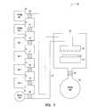
- FIG. 1depicts an atomic layer deposition system for fabricating a dielectric layer containing a zirconium-doped tantalum oxide, according to various embodiments of the present invention.
- FIG. 2illustrates a flow diagram of elements for an embodiment of a method to form a dielectric layer containing a zirconium-doped tantalum oxide, according to various embodiments of the present invention.
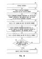
- FIG. 3illustrates a flow diagram of elements for an embodiment of a method to form a dielectric layer containing a zirconium-doped tantalum oxide, according to the present invention.
- FIG. 4illustrates a flow diagram of elements for an embodiment of a method to form a dielectric layer containing a zirconium-doped tantalum oxide, according to the present invention.
- FIG. 5illustrates a flow diagram of elements for an embodiment of a method to form a dielectric layer containing a zirconium-doped tantalum oxide including substituting a zirconium sequence for a tantalum sequence, according to the present invention.
- FIG. 6illustrates a flow diagram of elements for an embodiment of a method to form a dielectric layer containing a zirconium-doped tantalum oxide including commonly pulsing a zirconium precursor and a tantalum precursor, according to the present invention.
- FIG. 7shows an embodiment of a configuration of a transistor having a dielectric layer containing an atomic layer deposited zirconium-doped tantalum oxide, according to the present invention.
- FIG. 8shows an embodiment of a configuration of a transistor with a floating gate having a dielectric layer containing an atomic layer deposited zirconium-doped tantalum oxide, according to the present invention.
- FIG. 9shows an embodiment of a configuration of a capacitor having a dielectric layer containing an atomic layer deposited zirconium-doped tantalum oxide, according to the present invention.
- FIG. 10depicts an embodiment of a dielectric layer including a nanolaminate having at least one layer containing an atomic layer deposited zirconium-doped tantalum oxide, according to the present invention.
- FIG. 11is a simplified diagram for an embodiment of a controller coupled to an electronic device, according to the present invention.
- FIG. 12illustrates a diagram for an embodiment of an electronic system having devices with a dielectric film containing an atomic layer deposited zirconium-doped tantalum oxide, according to the present invention.
- wafer and substrate used in the following descriptioninclude any structure having an exposed surface with which to form an integrated circuit (IC) structure.
- substrateis understood to include semiconductor wafers.
- substrateis also used to refer to semiconductor structures during processing, and may include other layers that have been fabricated thereupon. Both wafer and substrate include doped and undoped semiconductors, epitaxial semiconductor layers supported by a base semiconductor or insulator, as well as other semiconductor structures well known to one skilled in the art.
- conductoris understood to generally include n-type and p-type semiconductors and the term insulator or dielectric is defined to include any material that is less electrically conductive than the materials referred to as conductors or as semiconductors.
- horizontalas used in this application is defined as a plane parallel to the conventional plane or surface of a wafer or substrate, regardless of the orientation of the wafer or substrate.
- verticalrefers to a direction perpendicular to the horizontal as defined above. Prepositions, such as “on”, “side” (as in “sidewall”), “higher”, “lower”, “over” and “under” are defined with respect to the conventional plane or surface being on the top surface of the wafer or substrate, regardless of the orientation of the wafer or substrate.
- a gate dielectric in a transistorhas both a physical gate dielectric thickness and an equivalent oxide thickness (t eq ).
- the equivalent oxide thicknessquantifies the electrical properties, such as capacitance, of the gate dielectric in terms of a representative physical thickness.
- t eqis defined as the thickness of a theoretical SiO 2 layer that would be required to have the same capacitance density as a given dielectric, ignoring leakage current and reliability considerations.
- a SiO 2 layer of thickness, t, deposited on a Si surface as a gate dielectricwill have a t eq larger than its thickness, t.
- This t eqresults from the capacitance in the surface channel on which the SiO 2 is deposited due to the formation of a depletion/inversion region.
- This depletion/inversion regioncan result in t eq being from 3 to 6 Angstroms ( ⁇ ) larger than the SiO 2 thickness, t.
- the gate dielectric equivalent oxide thicknessto under 10 ⁇
- the physical thickness requirement for a SiO 2 layer used for a gate dielectricwould be need to be approximately 4 to 7 ⁇ .
- SiO 2 layerAdditional requirements on a SiO 2 layer would depend on the gate electrode used in conjunction with the SiO 2 gate dielectric. Using a conventional polysilicon gate would result in an additional increase in t eq for the SiO 2 layer. This additional thickness could be eliminated by using a metal gate electrode, though metal gates are not currently used in typical complementary metal-oxide-semiconductor field effect transistor (CMOS) technology. Thus, future devices would be designed towards a physical SiO 2 gate dielectric layer of about 5 ⁇ or less. Such a small thickness requirement for a SiO 2 oxide layer creates additional problems.
- CMOScomplementary metal-oxide-semiconductor field effect transistor
- Silicon dioxideis used as a gate dielectric, in part, due to its electrical isolation properties in a SiO 2 —Si based structure. This electrical isolation is due to the relatively large band gap of SiO 2 (8.9 eV) making it a good insulator from electrical conduction. Signification reductions in its band gap would eliminate it as a material for a gate dielectric. As the thickness of a SiO 2 layer decreases, the number of atomic layers, or monolayers of the material in the thickness decreases. At a certain thickness, the number of monolayers will be sufficiently small that the SiO 2 layer will not have a complete arrangement of atoms as in a larger or bulk layer.
- a thin SiO 2 layer of only one or two monolayerswill not form a full band gap.
- the lack of a full band gap in a SiO 2 gate dielectricwould cause an effective short between an underlying Si channel and an overlying polysilicon gate.
- This undesirable propertysets a limit on the physical thickness to which a SiO 2 layer can be scaled.
- the minimum thickness due to this monolayer effectis thought to be about 7-8 ⁇ . Therefore, for future devices to have a t eg less than about 10 ⁇ , other dielectrics than SiO 2 need to be considered for use as a gate dielectric.
- materials with a dielectric constant greater than that of SiO 2 , 3.9will have a physical thickness that can be considerably larger than a desired t eq , while providing the desired equivalent oxide thickness.
- an alternate dielectric material with a dielectric constant of 10could have a thickness of about 25.6 ⁇ to provide a t eq of 10 ⁇ , not including any depletion/inversion layer effects.
- a reduced equivalent oxide thickness for transistorscan be realized by using dielectric materials with higher dielectric constants than SiO 2 .
- the thinner equivalent oxide thickness required for lower transistor operating voltages and smaller transistor dimensionsmay be realized by a significant number of materials, but additional fabricating requirements makes determining a suitable replacement for SiO 2 difficult.
- the current view for the microelectronics industryis still for Si based devices. This requires that the gate dielectric employed be grown on a silicon substrate or silicon layer, which places significant constraints on the substitute dielectric material.
- the dielectric on the silicon layerthere exists the possibility that a small layer of SiO 2 could be formed in addition to the desired dielectric.
- the resultwould effectively be a dielectric layer consisting of two sublayers in parallel with each other and the silicon layer on which the dielectric is formed. In such a case, the resulting capacitance would be that of two dielectrics in series.
- the t eq of the dielectric layerwould be the sum of the SiO 2 thickness and a multiplicative factor of the thickness, t, of the dielectric being formed, written as
- the t eqis again limited by a SiO 2 layer.
- the t eqwould be limited by the layer with the lowest dielectric constant.
- the layer interfacing with the silicon layermust provide a high quality interface to maintain a high channel carrier mobility.
- SiO 2as a gate dielectric
- Having an amorphous structure for a gate dielectricprovides for reducing problems of leakage current associated with grain boundaries in polycrystalline gate dielectrics that provide high leakage paths. Additionally, grain size and orientation changes throughout a polycrystalline gate dielectric can cause variations in the film's dielectric constant, along with uniformity and surface topography problems.
- materials having the advantage of a high dielectric constant relative to SiO 2also have the disadvantage of a crystalline form, at least in a bulk configuration.
- the best candidates for replacing SiO 2 as a gate dielectricare those with high dielectric constant, which can be fabricated as a thin layer with an amorphous form.
- High- ⁇ materialsinclude materials having a dielectric constant greater than silicon dioxide, for example, dielectrics materials having a dielectric constant greater than about twice the dielectric constant of silicon dioxide.
- a dopantBy introducing a dopant into a high- ⁇ metal oxide dielectric, its amorphous-to-polycrystalline temperature can be increased. The dopant acts to disturb the ordered structure of the original film.
- Elements usable as dopants in some high- ⁇ materialshave include Si, Al, Zr, Hf, and N. By adjusting the amount of the dopants in the original film, the physical and electrical properties of such metal oxides may be tailored.
- Bulk (Ta 2 O 5 ) 1 ⁇ x (Zr 2 O) x polycrystalline ceramicsformed by mixing powders of Ta 2 O 5 and Zr 2 O and sintering at high temperatures, have increased dielectric constants with respect to Ta 2 O 5 for certain amounts of Zr in the bulk (Ta 2 O 5 ) 1 ⁇ x (Zr 2 O) x structure.
- An appropriate high- ⁇ gate dielectricshould have a large energy gap (E g ) and large energy barrier heights with Si for both electrons and holes.
- the bandgapis inversely related to the dielectric constant for a high- ⁇ material, which lessens some advantages of the high- ⁇ material.
- Tantalum oxide (Ta 2 O 5 )is a potential replacement for SiO 2 . It has a bandgap of about 4.5 eV and a dielectric constant of about 26. Further, Ta 2 O 5 is a suitable candidate for engineering its physical and electrical properties by doping, since its structure does not change significantly with the addition of a substantial amount of another oxide.
- forming Ta 2 O 5 on a silicon substratemay result in an interface layer that contains SiO 2 , in particular at processing temperatures above 700° C.
- the material composition and its properties of an interface layerare typically dependent on process conditions and the condition of the substrate before forming the dielectric layer.
- a SiO 2 interface layer or other composition interface layermay improve the interface density, fixed charge density, and channel mobility of a device having this interface layer.
- An embodiment for a method for forming a dielectric layerincludes forming a dielectric film containing a zirconium-doped tantalum oxide by depositing tantalum on a substrate surface by atomic layer deposition and by depositing zirconium by atomic layer deposition on the substrate surface.
- Embodimentsinclude structures for capacitors, transistors, memory devices, and electronic systems with dielectric layers containing atomic layer deposited zirconium-doped tantalum oxide, and methods for forming such structures.
- Embodiments for foaming a tantalum oxide layer, or film, by atomic layer depositioninclude doping the tantalum oxide with zirconium.
- An undoped tantalum oxide filmmay be a film having a specific stoichiometry such as Ta 2 O 5 or it may be a non-stoichiometric tantalum oxide, Ta y O x , which is represented herein as TaO x .
- the resulting filmmay be considered TaO x doped with Zr or ZrO x .
- Embodiments of dielectric layers containing an atomic layer deposited zirconium-doped tantalum oxide layerhave a larger dielectric constant than silicon dioxide. Such dielectric layers provide a significantly thinner equivalent oxide thickness compared with a silicon oxide layer having the same physical thickness. Alternately, such dielectric layers provide a significantly thicker physical thickness than a silicon oxide layer having the same equivalent oxide thickness. This increased physical thickness aids in reducing leakage current.
- Another consideration for selecting the material and method for forming a dielectric film for use in electronic devices and systemsconcerns the roughness of a dielectric film on a substrate.
- Surface roughness of the dielectric filmhas a significant effect on the electrical properties of the gate oxide, and the resulting operating characteristics of the transistor.
- the leakage current through a physical 1.0 nm gate oxideincreases by a factor of 10 for every 0.1 increase in the root-mean-square (RMS) roughness.
- particles of the material to be depositedbombard the surface at a high energy. When a particle hits the surface, some particles adhere, and other particles cause damage. High energy impacts remove body region particles creating pits.
- the surface of such a deposited layercan have a rough contour due to the rough interface at the body region.
- a zirconium-doped tantalum oxide dielectric film having a substantially smooth surface relative to other processing techniquesis formed using atomic layer deposition (ALD). Further, forming such a dielectric film using atomic layer deposition can provide for controlling transitions between material layers. Thus, atomic layer deposited zirconium-doped tantalum oxide dielectric films can have an engineered transition with a substrate surface.
- ALDatomic layer deposition
- ALDalso known as atomic layer epitaxy (ALE)
- ALEatomic layer epitaxy
- CVDchemical vapor deposition
- ALDalternatively pulsed-CVD
- gaseous precursorsare introduced one at a time to the substrate surface mounted within a reaction chamber (or reactor). This introduction of the gaseous precursors takes the form of pulses of each gaseous precursor.
- the precursor gasis made to flow into a specific area or region for a short period of time.
- the reaction chamberis purged with a gas, which in many cases is an inert gas, and/or evacuated.
- CS-ALDchemisorption-saturated ALD
- the second pulsing phaseintroduces another precursor on the substrate where the growth reaction of the desired film takes place. Subsequent to the film growth reaction, reaction byproducts and precursor excess are purged from the reaction chamber.
- precursor pulse timesrange from about 0.5 sec to about 2 to 3 seconds.
- ALDIn ALD, the saturation of all the reaction and purging phases makes the growth self-limiting. This self-limiting growth results in large area uniformity and conformality, which has important applications for such cases as planar substrates, deep trenches, and in the processing of porous silicon and high surface area silica and alumina powders.
- ALDprovides for controlling film thickness in a straightforward manner by controlling the number of growth cycles.
- ALDwas originally developed to manufacture luminescent and dielectric films needed in electroluminescent displays. Significant efforts have been made to apply ALD to the growth of doped zinc sulfide and alkaline earth metal sulfide films. Additionally, ALD has been studied for the growth of different epitaxial II-V and II-VI films, nonepitaxial crystalline or amorphous oxide and nitride films and multilayer structures of these. There also has been considerable interest towards the ALD growth of silicon and germanium films, but due to the difficult precursor chemistry, this has not been very successful.
- the precursors used in an ALD processmay be gaseous, liquid or solid. However, liquid or solid precursors should be volatile. The vapor pressure should be high enough for effective mass transportation. Also, solid and some liquid precursors may need to be heated inside the reaction chamber and introduced through heated tubes to the substrates. The necessary vapor pressure should be reached at a temperature below the substrate temperature to avoid the condensation of the precursors on the substrate. Due to the self-limiting growth mechanisms of ALD, relatively low vapor pressure solid precursors can be used though evaporation rates may somewhat vary during the process because of changes in their surface area.
- the precursorsshould be thermally stable at the substrate temperature because their decomposition would destroy the surface control and accordingly the advantages of the ALD method which relies on the reaction of the precursor at the substrate surface. A slight decomposition, if slow compared to the ALD growth, can be tolerated.
- the precursorsshould chemisorb on or react with the surface, though the interaction between the precursor and the surface as well as the mechanism for the adsorption is different for different precursors.
- the molecules at the substrate surfaceshould react aggressively with the second precursor to form the desired solid film. Additionally, precursors should not react with the film to cause etching, and precursors should not dissolve in the film. Using highly reactive precursors in ALD contrasts with the selection of precursors for conventional CVD.
- the by-products in the reactionshould be gaseous in order to allow their easy removal from the reaction chamber. Further, the by-products should not react or adsorb on the surface.
- RS-ALDreaction sequence ALD
- the self-limiting process sequenceinvolves sequential surface chemical reactions.
- RS-ALDrelies on chemistry between a reactive surface and a reactive molecular precursor.
- molecular precursorsare pulsed into the ALD reaction chamber separately.
- the metal precursor reaction at the substrateis typically followed by an inert gas pulse to remove excess precursor and by-products from the reaction chamber prior to pulsing the next precursor of the fabrication sequence.
- RS-ALDfilms can be layered in equal metered sequences that are all identical in chemical kinetics, deposition per cycle, composition, and thickness.
- RS-ALD sequencesgenerally deposit less than a full layer per cycle.
- a deposition or growth rate of about 0.25 to about 2.00 ⁇ per RS-ALD cyclecan be realized.
- RS-ALDThe advantages of RS-ALD include continuity at an interface avoiding poorly defined nucleating regions that are typical for chemical vapor deposition ( ⁇ 20 ⁇ ) and physical vapor deposition ( ⁇ 50 ⁇ ), conformality over a variety of substrate topologies, use of low temperature and mildly oxidizing processes, lack of dependence on the reaction chamber, growth thickness dependent solely on the number of cycles performed, and ability to engineer multilayer laminate films with resolution of one to two monolayers.
- RS-ALD processesRS-ALD allows for deposition control on the order on monolayers and the ability to deposit monolayers of amorphous films.
- a sequencerefers to the ALD material formation based on an ALD reaction of one precursor with its reactant precursor.
- forming tantalum oxide from a TaI 4 precursor and H 2 O 2forms an embodiment of a tantalum/oxygen sequence, which can also be referred to as tantalum sequence.
- a cycle of a sequenceincludes pulsing a precursor, pulsing a purging gas for the precursor, pulsing a reactant precursor, and pulsing the reactant's purging gas.
- a layer of zirconium-doped TaO xis formed on a substrate mounted in a reaction chamber using ALD in a repetitive sequence using precursor gases individually pulsed into the reaction chamber.
- ALDatomic layer deposition
- solid or liquid precursorscan be used in an appropriately designed reaction chamber.
- FIG. 1shows an embodiment of an atomic layer deposition system 100 for processing a dielectric film containing zirconium-doped tantalum oxide.
- a substrate 110is located inside a reaction chamber 120 of ALD system 100 .
- a heating element 130which is thermally coupled to substrate 110 to control the substrate temperature.
- a gas-distribution fixture 140introduces precursor gases to the substrate 110 .
- Each precursor gasoriginates from individual gas sources 151 - 154 whose flow is controlled by mass-flow controllers 156 - 159 , respectively.
- Gas sources 151 - 154provide a precursor gas either by storing the precursor as a gas or by providing a location and apparatus for evaporating a solid or liquid material to form the selected precursor gas.
- purging gas sources 161 , 162are also included in the ALD system.
- additional purging gas sourcescan be constructed in ALD system 100 , one purging gas source for each precursor gas, for example.
- Gas sources 151 - 154 and purging gas sources 161 - 162are coupled by their associated mass-flow controllers to a common gas line or conduit 170 which is coupled to the gas-distribution fixture 140 inside the reaction chamber 120 .
- Gas conduit 170is also coupled to vacuum pump, or exhaust pump, 181 by mass-flow controller 186 to remove excess precursor gases, purging gases, and by-product gases at the end of a purging sequence from the gas conduit.
- Vacuum pump, or exhaust pump, 182is coupled by mass-flow controller 187 to remove excess precursor gases, purging gases, and by-product gases at the end of a purging sequence from reaction chamber 120 .
- mass-flow controller 187to remove excess precursor gases, purging gases, and by-product gases at the end of a purging sequence from reaction chamber 120 .
- control displays, mounting apparatus, temperature sensing devices, substrate maneuvering apparatus, and necessary electrical connections as are known to those skilled in the artare not shown in FIG. 1 .
- ALD system 100is well suited for practicing the present invention, other ALD systems commercially available can be used.
- reaction chambersfor deposition of films are understood by those of ordinary skill in the art of semiconductor fabrication.
- the present inventionman be practiced on a variety of such reaction chambers without undue experimentation.
- one of ordinary skill in the artwill comprehend the necessary detection, measurement, and control techniques in the art of semiconductor fabrication upon reading the disclosure.
- ALD system 100can be controlled by a computer. To focus on the use of ALD system 100 in the various embodiments of the present invention, the computer is not shown. Those skilled in the art can appreciate that the individual elements such as pressure control, temperature control, and gas flow within ALD system 100 can be under computer control.
- FIG. 2illustrates a flow diagram of elements for an embodiment of a method to form a dielectric layer containing a zirconium-doped tantalum oxide.
- tantalumis deposited onto a substrate surface by atomic layer deposition.
- a number of precursors containing tantalummay be used to deposit the tantalum.
- the pulsing of the tantalum precursormay use a pulsing period that provides uniform coverage of a monolayer on the surface or may use a pulsing period that provides partial formation of a monolayer on the surface.
- zirconiumis deposited by atomic layer deposition on the substrate surface.
- a reaction precursormay be pulsed after each pulsing of the tantalum precursor to form TaO x and another reaction precursor may be pulsed after each pulsing of the zirconium precursor to dope the TaO x with ZrO x .
- the two reaction precursorsmay have a common composition.
- to provide zirconium atom dopingdeposition of the zirconium is not followed by a reaction precursor but by another pulsing of the tantalum precursor.
- a reaction precursor to provide an oxidizing precursormay be pulsed after tantalum and zirconium have deposited. Appropriate purging pulses are performed between the pulsing of each element bearing precursor and each reaction precursor.
- the pulsing of the tantalum and zirconium precursorsmay be regulated to provide a selected ratio of zirconium atoms to the sum of tantalum and zirconium atoms to provide a desired doping.
- FIG. 3illustrates a flow diagram of elements for an embodiment of a method to form a dielectric layer containing a zirconium-doped tantalum oxide.
- a tantalum containing precursoris pulsed to deposit tantalum onto a substrate surface.
- a number of precursors containing tantalummay be used to deposit the tantalum.
- an oxygen containing precursoris pulsed to deposit oxygen on the substrate surface.
- a number of precursors containing oxygenmay be used to deposit the oxygen.
- the tantalum on the substrate surface and the oxygenreact to form one or more monolayers or a portion of a monolayer of TaO x .
- Precursorsmay be used that contain tantalum and oxygen such that TaO x is deposited on the substrate surface in a single pulsing.
- Appropriate purging pulsesmay be generated between the pulsing of the tantalum bearing precursor and the pulsing of the oxygen bearing precursor.
- a number of cycles of the pulsing of the tantalum containing precursor and the pulsing of the oxygen containing precursoris repeated. The number of cycles depends on the monolayer coverage desired and the desired amount of the tantalum to be contained in the doped TaO x being processed.
- a zirconium cycleis substituted for one or more cycles of the pulsing of the tantalum containing precursor, where the zirconium containing precursor deposits zirconium onto the substrate surface.
- a number of precursors containing zirconium and a number of precursors containing oxygenmay be used to deposit ZrO x as the dopant for the TaO x film being formed. Cycles using a number of precursors containing zirconium without an oxidizing reaction precursor may be used to deposit Zr as the dopant for the TaO x film being formed.
- a variation to the repeated cyclesmay be made.
- the dopingis included in the atomic layer deposition process by pulsing a zirconium containing precursor and reactant precursor in place of one or more cycles of the tantalum sequence.
- Associated with the dopant cyclethere is also a growth rate substantially constant at a fixed number of angstroms per cycle, for constant environmental conditions in the reaction chamber and constant sequencing parameters in the dopant cycle.
- the growth rate for forming the zirconium-doped TaO x dielectric filmmay be substantially the same as for an undoped TaO x dielectric film.
- growth ratescan vary from that of an undoped TaO x dielectric film.
- particular growth ratescan be determined during normal initial testing of the ALD system for processing a zirconium-doped TaO x dielectric film for a given application without undue experimentation.
- FIG. 4illustrates a flow diagram of elements for an embodiment of a method to form a dielectric layer containing a zirconium-doped tantalum oxide.
- a tantalum containing precursoris pulsed to deposit tantalum onto a substrate surface. A number of precursors containing tantalum may be used to deposit the tantalum.
- a zirconium containing precursoris pulsed to deposit zirconium by atomic layer deposition. The zirconium containing precursor is pulsed during a portion of the time that the tantalum containing precursor is being pulsed. A number of precursors containing zirconium may be used to deposit the zirconium.
- a reaction precursoris pulsed. The reaction precursor provides an oxidizing reaction at the substrate surface to form TaO x doped with zirconium. The zirconium dopant may be ZrO x .
- the zirconium containing precursorcan be pulsed simultaneously with the tantalum containing precursor. Then, following a gas purge, a reactant precursor that provides an ALD reaction for both the tantalum containing precursor and the zirconium precursor is pulsed into the reaction.
- the percentage of the zirconiumcan be controlled by regulating the percentage of the zirconium containing precursor in the precursor mixture that is injected into the reaction chamber to the substrate. The growth per cycle would then depend on the growth rate using the given mixture. As can be understood by those skilled in the art, determining the growth rate for a particular mixture can be determined during normal initial testing of the ALD system for processing a zirconium-doped TaO x dielectric film without undue experimentation.
- Atomic layer deposition of the individual components of the zirconium-doped TaO x layerallows for individual control of each precursor pulsed into the reaction chamber.
- each precursoris pulsed into the reaction chamber for a predetermined period, where the predetermined period can be set separately for each precursor.
- each precursorcan be pulsed into the reaction under separate environmental conditions.
- the substratecan be maintained at a selected temperature and the reaction chamber maintained at a selected pressure independently for pulsing each precursor. Appropriate temperatures and pressures may be maintained, whether the precursor is a single precursor or a mixture of precursors.
- the pulsing of the precursor gasesis separated by purging the reaction chamber with a purging gas following each pulsing of a precursor.
- nitrogen gasis used as the purging gas following the pulsing of each precursor used in a cycle to form a film of zirconium-doped TaO x .
- the reaction chambercan also be purged by evacuating the reaction chamber.
- FIG. 5illustrates a flow diagram of elements for an embodiment of a method to form a dielectric layer containing a zirconium-doped tantalum oxide including substituting a zirconium sequence for a tantalum sequence.
- This embodimentcan be implemented with the atomic layer deposition system 100 of FIG. 1 .
- a substrate 110is prepared.
- the substrate used for forming a transistoris typically a silicon or silicon containing material. In other embodiments, germanium, gallium arsenide, silicon-on-sapphire substrates, or other suitable substrates may be used.
- This preparation processincludes cleaning substrate 110 and forming layers and regions of the substrate, such as drains and sources of a metal oxide semiconductor (MOS) transistor, prior to forming a gate dielectric.
- MOSmetal oxide semiconductor
- the substrateis cleaned to provide an initial substrate depleted of its native oxide.
- the initial substrateis cleaned to also provide a hydrogen-terminated surface.
- a silicon substrateundergoes a final HF rinse prior to ALD processing to provide the silicon substrate with a hydrogen-terminated surface without a native silicon oxide layer.
- the sequencing of the formation of the regions of the transistor being processedfollows typical sequencing that is generally performed in the fabrication of a MOS transistor as is well known to those skilled in the art. Included in the processing prior to forming a gate dielectric is the masking of substrate regions to be protected during the gate dielectric formation, as is typically performed in MOS fabrication. In this embodiment, the unmasked region includes a body region of a transistor, however one skilled in the art will recognize that other semiconductor device structures may utilize this process. Additionally, the substrate 110 in its ready for processing form is conveyed into a position in reaction chamber 120 for ALD processing.
- a tantalum containing precursoris pulsed into reaction chamber 120 .
- Ta(OC 2 H 5 ) 5is used as a precursor.
- the Ta(OC 2 H 5 ) 5is pulsed into reaction chamber 120 through the gas-distribution fixture 140 onto substrate 110 .
- the flow of the Ta(OC 2 H 5 ) 5is controlled by mass-flow controller 156 from gas source 151 , where the Ta(OC 2 H 5 ) 5 is maintained at about 105° C.
- the pressure in reaction chamberis at about 10 mbar nitrogen pressure.
- the substrate temperatureis maintained between about 250° C. and about 325° C. by heating element 130 . The upper bound of 325° C.
- a tantalum containing precursorincludes TaCl 5 .
- a first purging gasis pulsed into the reaction chamber 120 .
- nitrogenis used as a purging gas and a carrier gas.
- the nitrogen flowis controlled by mass-flow controller 166 from the purging gas source 161 into the gas conduit 170 .
- an oxygen containing precursoris pulsed into the reaction chamber 120 , at 520 .
- water vaporis selected as the precursor acting as a reactant to form TaO x on the substrate 110 .
- the H 2 O vaporis pulsed into the reaction chamber 120 through gas conduit 170 from gas source 152 by mass-flow controller 157 . The water vapor aggressively reacts at the surface of substrate 110 .
- a second purging gasis injected into the reaction chamber 120 , at 525 .
- Nitrogen gasis used to purge the reaction chamber after pulsing each precursor gas in the tantalum/oxygen sequence. Excess precursor gas, and reaction by-products are removed from the system by the purge gas in conjunction with the exhausting of the reaction chamber 120 using vacuum pump 182 through mass-flow controller 187 , and exhausting of the gas conduit 170 by the vacuum pump 181 through mass-flow controller 186 .
- the pulsing of the tantalum containing precursor, the pulsing of the oxygen containing precursor, and the pulsing of the first and second purging gasare repeated for a number of cycles.
- a zirconium containing precursoris pulsed into the reaction chamber 120 , at 535 .
- ZrI 4is used as the zirconium containing precursor.
- ZrCl 4may be used as the zirconium containing precursor.
- the ZrI 4 precursor having a purity of about 99.5% or greateris evaporated from a containment area held at about 240° C. in gas source 152 .
- Mass-flow controller 158regulates the pulsing of the ZrI 4 precursor to the surface of the substrate 110 through gas-distribution fixture 140 from gas source 152 .
- the substrate temperatureis maintained between about 230° C. and about 500° C. by heating element 130 .
- a third purging gasis introduced into the system.
- Nitrogen gascan also be used as a purging and carrier gas.
- the nitrogen flowis controlled by mass-flow controller 167 from the purging gas source 162 into the gas conduit 170 and subsequently into the reaction chamber 120 .
- argon gasis used as the purging gas.
- a reactant precursoris pulsed into the reaction chamber 120 , at 545 .
- the reactant precursoris selected to produce an oxidizing reaction for the zirconium at the substrate surface.
- the reactant precursoris H 2 O—H 2 O 2 vapor.
- Mass-flow controller 159regulates the H 2 O—H 2 O 2 vapor pulsing into reaction chamber 120 through gas conduit 170 from gas source 153 .
- the H 2 O—H 2 O 2 vaporaggressively reacts at the surface of substrate 110 .
- a fourth purging gasis injected into reaction chamber 120 , at 550 .
- Nitrogen gasmay be used to purge the reaction chamber after pulsing each precursor gas in the zirconium/oxygen sequence.
- argon gasmay be used as the purging gas.
- Excess precursor gas, and reaction by-productsare removed from the system by the purge gas in conjunction with the exhausting of reaction chamber 120 using vacuum pump 182 through mass-flow controller 187 , and exhausting of the gas conduit 170 by the vacuum pump 181 through mass-flow controller 186 .
- the substrateis held between about 230° C. and about 500° C. by the heating element 130 with reaction chamber 120 held at about 250 Pa.
- the ZrI 4 pulse timeis about 2.0 sec.
- the zirconium sequencecontinues with a purge pulse followed by a H 2 O—H 2 O 2 vapor pulse followed by a purge pulse.
- the H 2 O—H 2 O 2 vapor pulse timeis about 2.0 sec, and the ZrI 4 and the H 2 O—H 2 O 2 vapor purging pulse times are each at about 2.0 sec.
- the predetermined number of substitution cyclesis selected to set the percentage of zirconium dopant in the TaO x film. In an embodiment, the percentage is set ranging from about 5% to about 40% zirconium in the zirconium-doped TaO x film with respect to an atomic ratio of zirconium atoms to the sum of zirconium and tantalum atoms. If the number of completed substitution cycles is less than the predetermined number, the zirconium containing precursor is pulsed into the reaction chamber, at 535 , and the process continues.
- the dielectric film containing zirconium-doped TaO xmay optionally be annealed. The zirconium-doped TaO x film processed at these relatively low temperatures may provide an amorphous layer.
- the thickness of a zirconium-doped TaO x filmis determined by a fixed growth rate for the pulsing periods and precursors used, set at a value such as N nm/combined cycle, dependent upon the number of cycles of the zirconium sequence relative to the tantalum sequence that form a combined sequence.
- tin an application such as forming a gate dielectric of a MOS transistor, the ALD process is repeated for t/N total combined cycles. Once the t/N cycles have completed, no further ALD processing for zirconium-doped TaO x is required.
- the presence of residual chlorine in a zirconium-doped TaO x dielectric filmmay be reduced or eliminated providing a substantially chlorine free film by using metal precursors other than metal chlorides in the ALD processing of each metal, tantalum and zirconium.
- metal precursors other than metal chloridesin the ALD processing of each metal, tantalum and zirconium.
- Use of a metal iodine as a precursorresults in a film substantially free of residual iodine.
- metal halide precursors other than chloride metal precursorsmay be used. Eliminating residual chloride in such dielectric films may provide reduced leakage current for devices having these dielectric films.
- processing the device having the dielectric layer containing zirconium-doped TaO xis completed.
- completing the deviceincludes completing the formation of a transistor.
- completing the deviceincludes completing the formation of a capacitor.
- completing the processincludes completing the construction of a memory device having an array with access transistors formed with gate dielectrics containing atomic layer deposited zirconium-doped TaO x .
- completing the processincludes the formation of an electronic system including an information handling device that uses electronic devices with transistors formed with dielectric films containing atomic layer deposited zirconium-doped TaO x .
- information handling devicessuch as computers include many memory devices, having many access transistors.
- substituting a zirconium cycle for one or more cyclesincludes substituting a number of zirconium cycles to form a dielectric layer containing TaO x doped with a predetermined percentage (atomic ratio) for the zirconium ranging from about 5% to about 40% zirconium.
- the ALD processing of a zirconium-doped TaO x dielectric filmmay provide a dielectric film having a dielectric constant ranging from about 8 to about 27 depending upon the existence of an interface layer at the surface of the silicon surface.
- FIG. 6illustrates a flow diagram of elements for an embodiment of a method to form a dielectric layer containing a zirconium-doped tantalum oxide including commonly pulsing a zirconium precursor and a tantalum precursor.
- This embodimentcan be implemented with the atomic layer deposition system 100 of FIG. 1 .
- a substrate 110is prepared in a similar manner has at 505 in FIG. 5 .
- a tantalum containing precursoris pulsed into reaction chamber 120 , at 610 .
- a zirconium containing precursoris pulsed into reaction chamber 120 substantially simultaneously with the pulsing of the tantalum containing precursor, at 615 .
- the period for the zirconium containing precursormay be less than the period for the tantalum containing precursor.
- the mixture of the zirconium containing precursor and the tantalum containing precursoris regulated such that the zirconium acts as a dopant in a dielectric film containing the tantalum.
- a first purging gasis pulsed into reaction chamber 120 , at 620 .
- Excess precursor gases and reaction by-productsare removed from the system by the purge gas in conjunction with the exhausting of the reaction chamber 120 using vacuum pump 182 through mass-flow controller 187 , and exhausting of the gas conduit 170 by the vacuum pump 181 through mass-flow controller 186 .
- a reactant containing precursoris pulsed into reaction chamber 120 , at 625 .
- the reactant containing precursorprovides an oxidizing reaction at substrate 110 .
- a second purging gasis pulsed into reaction chamber 120 , at 630 . Completing the pulsing of the second purging gas into reaction chamber 120 completes one cycle for a tantalum-zirconium dopant sequence. Then, it is determined whether the total number of cycles for the tantalum-zirconium dopant sequence has been reached to form the desired thickness for a dielectric film containing zirconium-doped TaO x at 640 .
- the tantalum containing precursoris pulsed into reaction chamber, at 610 , and the process continues. If the total number of cycles to form the desired thickness has been completed, the dielectric film containing zirconium-doped TaO x can be annealed. The zirconium-doped TaO x formed is amorphous and remains amorphous after annealing.
- the thickness of a zirconium-doped TaO x filmis determined by a fixed growth rate for the pulsing periods and precursors used, set at a value such as N nm/cycle, dependent upon the tantalum precursor/zirconium dopant precursor mixture used.
- tzirconium-doped TaO x film thickness
- the ALD processis repeated for t/N total cycles. Once the t/N cycles have completed, no further ALD processing for zirconium-doped TaO x is required.
- the device having the dielectric layer containing zirconium-doped TaO xis completed, at 645 , in a similar manner as for 570 of FIG. 5 .
- pulsing a zirconium containing precursor into the reaction chamberincludes regulating the percentage of the zirconium containing precursor relative to the tantalum containing precursor to form a dielectric layer containing TaO x doped with a predetermined percentage of the zirconium.
- the zirconium-doped TaO x layermay be amorphous.
- the atomic ratio of zirconium to the sum of zirconium and tantalum atomsmay be regulated to select a dielectric constant in the range from about 8 to about 27.
- the selection of the dielectric constantmay be conducted in a optimization, or trade-off, process with improving the current leakage characteristics of the film.
- the embodiments described hereinprovide a process for growing a dielectric film having a wide range of useful equivalent oxide thickness, t eq , associated with a dielectric constant in the range from about 8 to about 27.
- This range of dielectric constantsprovides for a t eq ranging from about 14% to about 48% of a given silicon dioxide thickness.
- an embodiment for a zirconium-doped tantalum oxidemay be from two to seven times larger than the acceptable silicon dioxide thickness providing enhanced probability for reducing leakage current.
- dielectric films of zirconium-doped TaO x formed by atomic layer depositioncan provide not only thin t eq films, but also films with relatively low leakage current. Doping with zirconium yields a doped amorphous TaO x with enhanced leakage current characteristics.
- the novel processcan be implemented to form transistors, capacitors, memory devices, and other electronic systems including information handling devices.
- a transistor 700 as depicted in FIG. 7may be constructed by forming a source region 720 and a drain region 730 in a silicon based substrate 710 where source and drain regions 720 , 730 are separated by a body region 732 .
- Body region 732defines a channel having a channel length 734 .
- a dielectric layeris disposed on substrate 710 formed as a layer containing zirconium-doped tantalum oxide on substrate 710 in a reaction chamber by atomic layer deposition. The resulting dielectric layer forms gate dielectric 740 .
- a gate 750is formed over gate dielectric 740 .
- forming gate 750may include forming a polysilicon layer, though a metal gate may be formed in an alternative process.
- An interfacial layer 733may form between body region 732 and gate dielectric 740 .
- interfacial layer 733may be limited to a relatively small thickness compared to gate dielectric 740 , or to a thickness significantly less than gate dielectric 740 as to be effectively eliminated.
- Forming the substrate, the source and drain regions, and the gateis performed using standard processes known to those skilled in the art. Additionally, the sequencing of the various elements of the process for forming a transistor is conducted with standard fabrication processes, also as known to those skilled in the art.
- gate dielectric 740may be realized as a gate insulator in a silicon CMOS transistor.
- Use of a gate dielectric containing zirconium-doped tantalum oxideis not limited to silicon based substrates, but may be used with a variety of semiconductor substrates.
- FIG. 8shows an embodiment of a configuration of a transistor 800 having an atomic layer deposited zirconium-doped TaO x dielectric film.
- Transistor 800includes a silicon based substrate 810 with a source 820 and a drain 830 separated by a body region 832 .
- Body region 832 between source 820 and drain 830defines a channel region having a channel length 834 .
- Located above body region 832is a stack 855 including a gate dielectric 840 , a floating gate 852 , a floating gate dielectric 842 , and a control gate 850 .
- Gate dielectric 840includes a dielectric containing an atomic layer deposited zirconium-doped TaO x dielectric film as described herein with the remaining elements of the transistor 800 formed using processes known to those skilled in the art. Alternately, both gate dielectric 840 and floating gate dielectric 842 may be formed as dielectric layers containing an atomic layer deposited zirconium-doped TaO x dielectric film in various embodiments as described herein.
- An interfacial layer 833may form between body region 832 and gate dielectric 840 . In an embodiment, interfacial layer 833 may be limited to a relatively small thickness compared to gate dielectric 840 , or to a thickness significantly less than gate dielectric 840 as to be effectively eliminated.
- gate dielectric 840forms a tunnel gate insulator and floating gate dielectric 842 forms an inter-gate insulator in flash memory devices, where gate dielectric 840 and/or floating gate dielectric 842 have an atomic layer deposited zirconium-doped tantalum oxide film.
- Use of a gate dielectric and/or floating gate dielectric containing an atomic layer deposited zirconium-doped tantalum oxideis not limited to silicon based substrates, but may be used with a variety of semiconductor substrates.
- a methodincludes forming a first conductive layer 910 , forming a dielectric layer 920 containing an atomic layer deposited zirconium-doped TaO x film on first conductive layer 910 , and forming a second conductive layer 930 on dielectric layer 920 .
- the dielectric layer containing zirconium-doped TaO xmay be formed using any of the embodiments described herein.
- ALD formation of the zirconium-doped TaO x filmallows the zirconium to be selectively doped into the TaO x film within a predetermined range for the percentage of the zirconium in the film.
- An interfacial layer 915may form between first conductive layer 910 and dielectric layer 920 .
- interfacial layer 915may be limited to a relatively small thickness compared to dielectric layer 920 , or to a thickness significantly less than dielectric layer 920 as to be effectively eliminated.
- Embodiments for dielectric layer 920 containing an atomic layer deposited zirconium-doped TaO x in a capacitorincludes, but is not limited to, dielectrics in DRAM capacitors and as dielectrics in capacitors in analog, radio frequency (RF), and mixed signal integrated circuits.
- RFradio frequency
- a dielectric film containing atomic layer deposited zirconium-doped tantalum oxideprovide for enhanced device performance by providing devices with reduced leakage current. Further improvements in leakage current characteristics may be attained by forming one or more layers of an atomic layer deposited zirconium-doped tantalum oxide in a nanolaminate structure with other metal oxides such as TaO x and ZrO x . The transition from one layer of the nanolaminate to another layer of the nanolaminate provides further disruption to a tendency for an ordered structure in the nanolaminate stack.
- nanolaminatemeans a composite film of ultra thin layers of two or more materials in a layered stack, where the layers are alternating layers of materials of the composite film.
- each layer in a nanolaminatehas a thickness of an order of magnitude in the nanometer range.
- each individual material layer of the nanolaminatecan have a thickness as low as a monolayer of the material or as high as 20 nanometers.
- a TaO x /ZrO x /zirconium-doped TaO x nanolaminatecontains alternating layers of TaO x and ZrO x and zirconium-doped TaO x .
- FIG. 10depicts a nanolaminate structure 1000 for an embodiment of a dielectric structure including an atomic layer deposited zirconium-doped TaO x dielectric film.
- Nanolaminate structure 1000includes a plurality of layers 1005 - 1 , 1005 - 2 to 1005 -N, where at least one layer contains an atomic layer deposited zirconium-doped TaO x dielectric film.
- the other layersmay be other metal oxides such as TaO x and ZrO x .
- the sequencing of the layersdepends on the application.
- the effective dielectric constant associated with nanolaminate structure 1000is that attributable to N capacitors in series, where each capacitor has a thickness defined by the thickness of the corresponding layer.
- each thickness and the composition of each a nanolaminate structurecan be engineered to have a predetermined dielectric constant.
- Embodiments for structures such as nanolaminate structure 1000may be used as nanolaminate dielectrics in NROM flash memory devices as well as other integrated circuits.
- Transistors, capacitors, and other devices having dielectric films containing atomic layer deposited zirconium-doped TaO x formed by the methods described abovemay be implemented into memory devices and electronic systems including information handling devices.
- Embodiments of these information handling devicesmay include wireless systems, telecommunication systems, and computers.
- embodiments of electronic devices having dielectric films containing atomic layer deposited zirconium-doped tantalum oxidemay be realized as integrated circuits.
- FIG. 11illustrates a diagram for an electronic system 1100 having one or more devices with an embodiment for a dielectric layer containing atomic layer deposited zirconium-doped TaO x .
- Electronic system 1100includes a controller 1105 , a bus 1115 , and an electronic device 1125 , where bus 1115 provides electrical conductivity between controller 1105 and electronic device 1125 .
- controller 1005 and/or electronic device 1125include an embodiment for a dielectric layer containing atomic layer deposited zirconium-doped TaO x as previously discussed herein.
- Electronic system 1100may include, but is not limited to, information handling devices, wireless systems, telecommunication systems, fiber optic systems, electro-optic systems, and computers.
- FIG. 12depicts a diagram of an embodiment of a system 1200 having a controller 1205 and a memory 1225 .
- Controller 1205 and/or memory 1225may include a dielectric layer having an atomic layer deposited zirconium-doped TaO x .
- System 1200also includes an electronic apparatus 1235 , and a bus 1215 , where bus 1215 provides electrical conductivity between controller 1205 and electronic apparatus 1235 , and between controller 1205 and memory 1225 .
- Bus 1215may include an address, a data bus, and a control bus, each independently configured. Alternately, bus 1215 may use common conductive lines for providing address, data, and/or control, the use of which is regulated by controller 1205 .
- electronic apparatus 1235may be additional memory configured similar as memory 1225 .
- An embodimentmay include an additional peripheral device or devices 1245 coupled to bus 1215 .
- controller 1205is a processor. Any of controller 1205 , memory 1225 , bus 1215 , electronic apparatus 1235 , and peripheral device devices 1245 may include a dielectric layer having an atomic layer deposited zirconium-doped TaO x .
- System 1200may include, but is not limited to, information handling devices, telecommunication systems, and computers.
- Peripheral devices 1245may include displays, additional storage memory, or other control devices that may operate in conjunction with controller 1205 . Alternately, peripheral devices 1245 may include displays, additional storage memory, or other control devices that may operate in conjunction with controller 1205 and/or memory 1225 .
- Memory 1225may be realized as a memory device containing an atomic layer deposited zirconium-doped TaO x , dielectric layer. It will be understood that embodiments are equally applicable to any size and type of memory circuit and are not intended to be limited to a particular type of memory device. Memory types include a DRAM, SRAM (Static Random Access Memory) or Flash memories.
- the DRAMcould be a synchronous DRAM commonly referred to as SGRAM (Synchronous Graphics Random Access Memory), SDRAM (Synchronous Dynamic Random Access Memory), SDRAM II, and DDR SDRAM (Double Data Rate SDRAM), as well as Synchlink or Rambus DRAMs and other emerging DRAM technologies.
- SGRAMSynchronous Graphics Random Access Memory
- SDRAMSynchronous Dynamic Random Access Memory
- SDRAM IISynchroble Data Rate SDRAM
- DDR SDRAMDouble Data Rate SDRAM
- Zirconium-doped tantalum oxide films formed by atomic layer deposition processed in relatively low temperaturescan be amorphous and possess smooth surfaces. Such zirconium-doped tantalum oxide films can provide enhanced electrical properties due to their smoother surface resulting in reduced leakage current. Additionally, zirconium-doped tantalum oxide films by atomic layer deposition may also provide reduced leakage current while providing an increased dielectric constant as compared with undoped tantalum oxide and pure zirconium oxide layers. Additionally, such dielectric layers provide a significantly thicker physical thickness than a silicon oxide layer having the same equivalent oxide thickness, where the increased thickness would also reduce leakage current. These properties of layers containing atomic layer deposited zirconium-doped tantalum oxide films allow for application as dielectric layers in numerous electronic devices and systems.
- Capacitors, transistors, higher level ICs or devices including memory devices, and electronic systemsare constructed utilizing the novel process for forming a dielectric film having an ultra thin equivalent oxide thickness, t eq .
- Gate dielectric layers or films containing atomic layer deposited zirconium-doped tantalum oxideare formed having a dielectric constant ( ⁇ ) substantially higher than that of silicon oxide, such that these dielectric films are capable of a t eq thinner than SiO 2 gate dielectrics of the same physical thickness.
- the high dielectric constant relative to silicon dioxideallows the use of much larger physical thickness of these high-K dielectric materials for the same t eq of SiO 2 . Forming the relatively larger thickness aids in processing gate dielectrics and other dielectric layers in electronic devices and systems.
Landscapes
- Chemical & Material Sciences (AREA)
- Engineering & Computer Science (AREA)
- Chemical Kinetics & Catalysis (AREA)
- Organic Chemistry (AREA)
- Metallurgy (AREA)
- Mechanical Engineering (AREA)
- Materials Engineering (AREA)
- General Chemical & Material Sciences (AREA)
- Computer Hardware Design (AREA)
- Power Engineering (AREA)
- Microelectronics & Electronic Packaging (AREA)
- Physics & Mathematics (AREA)
- Manufacturing & Machinery (AREA)
- General Physics & Mathematics (AREA)
- Condensed Matter Physics & Semiconductors (AREA)
- Inorganic Chemistry (AREA)
- Formation Of Insulating Films (AREA)
- Semiconductor Memories (AREA)
- Insulated Gate Type Field-Effect Transistor (AREA)
- Chemical Vapour Deposition (AREA)
Abstract
Description
- This application is a continuation of U.S. application Ser. No. 11/608,281, filed Dec. 8, 2006, which is a divisional of U.S. application Ser. No. 10/909,959 filed Aug. 2, 2004, now issued as U.S. Pat. No. 7,601,649, which applications are incorporated herein by reference in their entirety.
- This application relates generally to semiconductor devices and device fabrication and, more particularly, to dielectric layers and their method of fabrication.
- The semiconductor device industry has a market driven need to improve speed performance, improve its low static (off-state) power requirements, and lower production costs for its silicon based microelectronic products. In particular, there is continuous pressure to reduce the size of devices such as transistors. To reduce transistor size, the thickness of the silicon dioxide, SiO2, gate dielectric is reduced in proportion to the shrinkage of the gate length. For example, a metal-oxide-semiconductor field effect transistor (MOSFET) would use a 1.5 nm thick SiO2gate dielectric for a gate length of 70 nm. The ultimate goal is to fabricate increasingly smaller and more reliable integrated circuits (ICs) for use in products such as processor chips, mobile telephones, and memory devices such as dynamic random access memories (DRAMs).
- Currently, the semiconductor industry relies on the ability to reduce or scale the dimensions of its basic devices, primarily, the silicon based MOSFET. This device scaling includes scaling the gate dielectric, which has primarily been fabricated using silicon dioxide. A thermally grown amorphous SiO2layer provides an electrically and thermodynamically stable material, where the interface of the SiO2layer with underlying silicon provides a high quality interface as well as superior electrical isolation properties. However, increased scaling and other requirements in microelectronic devices have created the need to use other dielectric materials as gate dielectrics.
FIG. 1 depicts an atomic layer deposition system for fabricating a dielectric layer containing a zirconium-doped tantalum oxide, according to various embodiments of the present invention.FIG. 2 illustrates a flow diagram of elements for an embodiment of a method to form a dielectric layer containing a zirconium-doped tantalum oxide, according to various embodiments of the present invention.FIG. 3 illustrates a flow diagram of elements for an embodiment of a method to form a dielectric layer containing a zirconium-doped tantalum oxide, according to the present invention.FIG. 4 illustrates a flow diagram of elements for an embodiment of a method to form a dielectric layer containing a zirconium-doped tantalum oxide, according to the present invention.FIG. 5 illustrates a flow diagram of elements for an embodiment of a method to form a dielectric layer containing a zirconium-doped tantalum oxide including substituting a zirconium sequence for a tantalum sequence, according to the present invention.FIG. 6 illustrates a flow diagram of elements for an embodiment of a method to form a dielectric layer containing a zirconium-doped tantalum oxide including commonly pulsing a zirconium precursor and a tantalum precursor, according to the present invention.FIG. 7 shows an embodiment of a configuration of a transistor having a dielectric layer containing an atomic layer deposited zirconium-doped tantalum oxide, according to the present invention.FIG. 8 shows an embodiment of a configuration of a transistor with a floating gate having a dielectric layer containing an atomic layer deposited zirconium-doped tantalum oxide, according to the present invention.FIG. 9 shows an embodiment of a configuration of a capacitor having a dielectric layer containing an atomic layer deposited zirconium-doped tantalum oxide, according to the present invention.FIG. 10 depicts an embodiment of a dielectric layer including a nanolaminate having at least one layer containing an atomic layer deposited zirconium-doped tantalum oxide, according to the present invention.FIG. 11 is a simplified diagram for an embodiment of a controller coupled to an electronic device, according to the present invention.FIG. 12 illustrates a diagram for an embodiment of an electronic system having devices with a dielectric film containing an atomic layer deposited zirconium-doped tantalum oxide, according to the present invention.- The following detailed description refers to the accompanying drawings that show, by way of illustration, specific aspects and embodiments in which the present invention may be practiced. These embodiments are described in sufficient detail to enable those skilled in the art to practice the present invention. Other embodiments may be utilized and structural, logical, and electrical changes may be made without departing from the scope of the present invention. The various embodiments disclosed herein are not necessarily mutually exclusive, as some disclosed embodiments can be combined with one or more other disclosed embodiments to form new embodiments.
- The terms wafer and substrate used in the following description include any structure having an exposed surface with which to form an integrated circuit (IC) structure. The term substrate is understood to include semiconductor wafers. The term substrate is also used to refer to semiconductor structures during processing, and may include other layers that have been fabricated thereupon. Both wafer and substrate include doped and undoped semiconductors, epitaxial semiconductor layers supported by a base semiconductor or insulator, as well as other semiconductor structures well known to one skilled in the art. The term conductor is understood to generally include n-type and p-type semiconductors and the term insulator or dielectric is defined to include any material that is less electrically conductive than the materials referred to as conductors or as semiconductors.
- The term “horizontal” as used in this application is defined as a plane parallel to the conventional plane or surface of a wafer or substrate, regardless of the orientation of the wafer or substrate. The term “vertical” refers to a direction perpendicular to the horizontal as defined above. Prepositions, such as “on”, “side” (as in “sidewall”), “higher”, “lower”, “over” and “under” are defined with respect to the conventional plane or surface being on the top surface of the wafer or substrate, regardless of the orientation of the wafer or substrate. The following detailed description is, therefore, not to be taken in a limiting sense, and the scope of the present invention is defined only by the appended claims, along with the full scope of equivalents to which such claims are entitled.
- A gate dielectric in a transistor has both a physical gate dielectric thickness and an equivalent oxide thickness (teq). The equivalent oxide thickness quantifies the electrical properties, such as capacitance, of the gate dielectric in terms of a representative physical thickness. teqis defined as the thickness of a theoretical SiO2layer that would be required to have the same capacitance density as a given dielectric, ignoring leakage current and reliability considerations.
- A SiO2layer of thickness, t, deposited on a Si surface as a gate dielectric will have a teqlarger than its thickness, t. This teqresults from the capacitance in the surface channel on which the SiO2is deposited due to the formation of a depletion/inversion region. This depletion/inversion region can result in teqbeing from 3 to 6 Angstroms (Å) larger than the SiO2thickness, t. Thus, with the semiconductor industry driving to someday scale the gate dielectric equivalent oxide thickness to under 10 Å, the physical thickness requirement for a SiO2layer used for a gate dielectric would be need to be approximately 4 to 7 Å.
- Additional requirements on a SiO2layer would depend on the gate electrode used in conjunction with the SiO2gate dielectric. Using a conventional polysilicon gate would result in an additional increase in teqfor the SiO2layer. This additional thickness could be eliminated by using a metal gate electrode, though metal gates are not currently used in typical complementary metal-oxide-semiconductor field effect transistor (CMOS) technology. Thus, future devices would be designed towards a physical SiO2gate dielectric layer of about 5 Å or less. Such a small thickness requirement for a SiO2oxide layer creates additional problems.
- Silicon dioxide is used as a gate dielectric, in part, due to its electrical isolation properties in a SiO2—Si based structure. This electrical isolation is due to the relatively large band gap of SiO2(8.9 eV) making it a good insulator from electrical conduction. Signification reductions in its band gap would eliminate it as a material for a gate dielectric. As the thickness of a SiO2layer decreases, the number of atomic layers, or monolayers of the material in the thickness decreases. At a certain thickness, the number of monolayers will be sufficiently small that the SiO2layer will not have a complete arrangement of atoms as in a larger or bulk layer. As a result of incomplete formation relative to a bulk structure, a thin SiO2layer of only one or two monolayers will not form a full band gap. The lack of a full band gap in a SiO2gate dielectric would cause an effective short between an underlying Si channel and an overlying polysilicon gate. This undesirable property sets a limit on the physical thickness to which a SiO2layer can be scaled. The minimum thickness due to this monolayer effect is thought to be about 7-8 Å. Therefore, for future devices to have a tegless than about 10 Å, other dielectrics than SiO2need to be considered for use as a gate dielectric.
- For a typical dielectric layer used as a gate dielectric, the capacitance is determined as one for a parallel plate capacitance: C=κε0A/t, where κ is the dielectric constant, ε0is the permittivity of free space, A is the area of the capacitor, and t is the thickness of the dielectric. The thickness, t, of a material is related to its teqfor a given capacitance, with SiO2having a dielectric constant κox=3.9, as
t=(κ/κox)teq=(κ/3.9)teq.- Thus, materials with a dielectric constant greater than that of SiO2, 3.9, will have a physical thickness that can be considerably larger than a desired teq, while providing the desired equivalent oxide thickness. For example, an alternate dielectric material with a dielectric constant of 10 could have a thickness of about 25.6 Å to provide a teqof 10 Å, not including any depletion/inversion layer effects. Thus, a reduced equivalent oxide thickness for transistors can be realized by using dielectric materials with higher dielectric constants than SiO2.
- The thinner equivalent oxide thickness required for lower transistor operating voltages and smaller transistor dimensions may be realized by a significant number of materials, but additional fabricating requirements makes determining a suitable replacement for SiO2difficult. The current view for the microelectronics industry is still for Si based devices. This requires that the gate dielectric employed be grown on a silicon substrate or silicon layer, which places significant constraints on the substitute dielectric material. During the formation of the dielectric on the silicon layer, there exists the possibility that a small layer of SiO2could be formed in addition to the desired dielectric. The result would effectively be a dielectric layer consisting of two sublayers in parallel with each other and the silicon layer on which the dielectric is formed. In such a case, the resulting capacitance would be that of two dielectrics in series. As a result, the teqof the dielectric layer would be the sum of the SiO2thickness and a multiplicative factor of the thickness, t, of the dielectric being formed, written as
teq=tSiO2 +(κox/κ)t.- Thus, if a SiO2layer is formed in the process, the teqis again limited by a SiO2layer. In the event that a barrier layer is formed between the silicon layer and the desired dielectric in which the barrier layer prevents the formation of a SiO2layer, the teqwould be limited by the layer with the lowest dielectric constant. However, whether a single dielectric layer with a high dielectric constant or a barrier layer with a higher dielectric constant than SiO2is employed, the layer interfacing with the silicon layer must provide a high quality interface to maintain a high channel carrier mobility.
- One of the advantages using SiO2as a gate dielectric has been that the formation of the SiO2layer results in an amorphous gate dielectric. Having an amorphous structure for a gate dielectric provides for reducing problems of leakage current associated with grain boundaries in polycrystalline gate dielectrics that provide high leakage paths. Additionally, grain size and orientation changes throughout a polycrystalline gate dielectric can cause variations in the film's dielectric constant, along with uniformity and surface topography problems. Typically, materials having the advantage of a high dielectric constant relative to SiO2also have the disadvantage of a crystalline form, at least in a bulk configuration. The best candidates for replacing SiO2as a gate dielectric are those with high dielectric constant, which can be fabricated as a thin layer with an amorphous form.
- High-κ materials include materials having a dielectric constant greater than silicon dioxide, for example, dielectrics materials having a dielectric constant greater than about twice the dielectric constant of silicon dioxide. By introducing a dopant into a high-κ metal oxide dielectric, its amorphous-to-polycrystalline temperature can be increased. The dopant acts to disturb the ordered structure of the original film. Elements usable as dopants in some high-κ materials have include Si, Al, Zr, Hf, and N. By adjusting the amount of the dopants in the original film, the physical and electrical properties of such metal oxides may be tailored. Bulk (Ta2O5)1−x(Zr2O)xpolycrystalline ceramics, formed by mixing powders of Ta2O5and Zr2O and sintering at high temperatures, have increased dielectric constants with respect to Ta2O5for certain amounts of Zr in the bulk (Ta2O5)1−x(Zr2O)xstructure.
- An appropriate high-κ gate dielectric should have a large energy gap (Eg) and large energy barrier heights with Si for both electrons and holes. Generally, the bandgap is inversely related to the dielectric constant for a high-κ material, which lessens some advantages of the high-κ material. Tantalum oxide (Ta2O5) is a potential replacement for SiO2. It has a bandgap of about 4.5 eV and a dielectric constant of about 26. Further, Ta2O5is a suitable candidate for engineering its physical and electrical properties by doping, since its structure does not change significantly with the addition of a substantial amount of another oxide. However, forming Ta2O5on a silicon substrate may result in an interface layer that contains SiO2, in particular at processing temperatures above 700° C. The material composition and its properties of an interface layer are typically dependent on process conditions and the condition of the substrate before forming the dielectric layer. Though the existence of an interface layer may effectively reduce the dielectric constant associated with the dielectric layer and its substrate interface layer, a SiO2interface layer or other composition interface layer, may improve the interface density, fixed charge density, and channel mobility of a device having this interface layer.
- An embodiment for a method for forming a dielectric layer includes forming a dielectric film containing a zirconium-doped tantalum oxide by depositing tantalum on a substrate surface by atomic layer deposition and by depositing zirconium by atomic layer deposition on the substrate surface. Embodiments include structures for capacitors, transistors, memory devices, and electronic systems with dielectric layers containing atomic layer deposited zirconium-doped tantalum oxide, and methods for forming such structures.
- Embodiments for foaming a tantalum oxide layer, or film, by atomic layer deposition include doping the tantalum oxide with zirconium. An undoped tantalum oxide film may be a film having a specific stoichiometry such as Ta2O5or it may be a non-stoichiometric tantalum oxide, TayOx, which is represented herein as TaOx. The zirconium doping may be performed as a doping by zirconium atoms or by zirconium oxide ZrOx, where x may be x=2. The resulting film may be considered TaOxdoped with Zr or ZrOx.
- Embodiments of dielectric layers containing an atomic layer deposited zirconium-doped tantalum oxide layer have a larger dielectric constant than silicon dioxide. Such dielectric layers provide a significantly thinner equivalent oxide thickness compared with a silicon oxide layer having the same physical thickness. Alternately, such dielectric layers provide a significantly thicker physical thickness than a silicon oxide layer having the same equivalent oxide thickness. This increased physical thickness aids in reducing leakage current.
- Another consideration for selecting the material and method for forming a dielectric film for use in electronic devices and systems concerns the roughness of a dielectric film on a substrate. Surface roughness of the dielectric film has a significant effect on the electrical properties of the gate oxide, and the resulting operating characteristics of the transistor. The leakage current through a physical 1.0 nm gate oxide increases by a factor of 10 for every 0.1 increase in the root-mean-square (RMS) roughness.
- During a conventional sputtering deposition process stage, particles of the material to be deposited bombard the surface at a high energy. When a particle hits the surface, some particles adhere, and other particles cause damage. High energy impacts remove body region particles creating pits. The surface of such a deposited layer can have a rough contour due to the rough interface at the body region.
- In an embodiment, a zirconium-doped tantalum oxide dielectric film having a substantially smooth surface relative to other processing techniques is formed using atomic layer deposition (ALD). Further, forming such a dielectric film using atomic layer deposition can provide for controlling transitions between material layers. Thus, atomic layer deposited zirconium-doped tantalum oxide dielectric films can have an engineered transition with a substrate surface.
- ALD, also known as atomic layer epitaxy (ALE), is a modification of chemical vapor deposition (CVD) and is also called “alternatively pulsed-CVD.” In ALD, gaseous precursors are introduced one at a time to the substrate surface mounted within a reaction chamber (or reactor). This introduction of the gaseous precursors takes the form of pulses of each gaseous precursor. In a pulse of a precursor gas, the precursor gas is made to flow into a specific area or region for a short period of time. Between the pulses, the reaction chamber is purged with a gas, which in many cases is an inert gas, and/or evacuated.
- In a chemisorption-saturated ALD (CS-ALD) process, during the first pulsing phase, reaction with the substrate occurs with the precursor saturatively chemisorbed at the substrate surface. Subsequent pulsing with a purging gas removes precursor excess from the reaction chamber.
- The second pulsing phase introduces another precursor on the substrate where the growth reaction of the desired film takes place. Subsequent to the film growth reaction, reaction byproducts and precursor excess are purged from the reaction chamber. With favourable precursor chemistry where the precursors adsorb and react with each other on the substrate aggressively, one ALD cycle can be preformed in less than one second in properly designed flow type reaction chambers. Typically, precursor pulse times range from about 0.5 sec to about 2 to 3 seconds.
- In ALD, the saturation of all the reaction and purging phases makes the growth self-limiting. This self-limiting growth results in large area uniformity and conformality, which has important applications for such cases as planar substrates, deep trenches, and in the processing of porous silicon and high surface area silica and alumina powders. Significantly, ALD provides for controlling film thickness in a straightforward manner by controlling the number of growth cycles.
- ALD was originally developed to manufacture luminescent and dielectric films needed in electroluminescent displays. Significant efforts have been made to apply ALD to the growth of doped zinc sulfide and alkaline earth metal sulfide films. Additionally, ALD has been studied for the growth of different epitaxial II-V and II-VI films, nonepitaxial crystalline or amorphous oxide and nitride films and multilayer structures of these. There also has been considerable interest towards the ALD growth of silicon and germanium films, but due to the difficult precursor chemistry, this has not been very successful.
- The precursors used in an ALD process may be gaseous, liquid or solid. However, liquid or solid precursors should be volatile. The vapor pressure should be high enough for effective mass transportation. Also, solid and some liquid precursors may need to be heated inside the reaction chamber and introduced through heated tubes to the substrates. The necessary vapor pressure should be reached at a temperature below the substrate temperature to avoid the condensation of the precursors on the substrate. Due to the self-limiting growth mechanisms of ALD, relatively low vapor pressure solid precursors can be used though evaporation rates may somewhat vary during the process because of changes in their surface area.
- There are several other requirements for precursors used in ALD. The precursors should be thermally stable at the substrate temperature because their decomposition would destroy the surface control and accordingly the advantages of the ALD method which relies on the reaction of the precursor at the substrate surface. A slight decomposition, if slow compared to the ALD growth, can be tolerated.
- The precursors should chemisorb on or react with the surface, though the interaction between the precursor and the surface as well as the mechanism for the adsorption is different for different precursors. The molecules at the substrate surface should react aggressively with the second precursor to form the desired solid film. Additionally, precursors should not react with the film to cause etching, and precursors should not dissolve in the film. Using highly reactive precursors in ALD contrasts with the selection of precursors for conventional CVD.
- The by-products in the reaction should be gaseous in order to allow their easy removal from the reaction chamber. Further, the by-products should not react or adsorb on the surface.
- In a reaction sequence ALD (RS-ALD) process, the self-limiting process sequence involves sequential surface chemical reactions. RS-ALD relies on chemistry between a reactive surface and a reactive molecular precursor. In an RS-ALD process, molecular precursors are pulsed into the ALD reaction chamber separately. The metal precursor reaction at the substrate is typically followed by an inert gas pulse to remove excess precursor and by-products from the reaction chamber prior to pulsing the next precursor of the fabrication sequence.
- By RS-ALD, films can be layered in equal metered sequences that are all identical in chemical kinetics, deposition per cycle, composition, and thickness. RS-ALD sequences generally deposit less than a full layer per cycle. Typically, a deposition or growth rate of about 0.25 to about 2.00 Å per RS-ALD cycle can be realized.
- The advantages of RS-ALD include continuity at an interface avoiding poorly defined nucleating regions that are typical for chemical vapor deposition (<20 Å) and physical vapor deposition (<50 Å), conformality over a variety of substrate topologies, use of low temperature and mildly oxidizing processes, lack of dependence on the reaction chamber, growth thickness dependent solely on the number of cycles performed, and ability to engineer multilayer laminate films with resolution of one to two monolayers. RS-ALD processes RS-ALD allows for deposition control on the order on monolayers and the ability to deposit monolayers of amorphous films.
- Herein, a sequence refers to the ALD material formation based on an ALD reaction of one precursor with its reactant precursor. For example, forming tantalum oxide from a TaI4precursor and H2O2, as its reactant precursor, forms an embodiment of a tantalum/oxygen sequence, which can also be referred to as tantalum sequence. A cycle of a sequence includes pulsing a precursor, pulsing a purging gas for the precursor, pulsing a reactant precursor, and pulsing the reactant's purging gas.
- In an embodiment, a layer of zirconium-doped TaOxis formed on a substrate mounted in a reaction chamber using ALD in a repetitive sequence using precursor gases individually pulsed into the reaction chamber. Alternately, solid or liquid precursors can be used in an appropriately designed reaction chamber.
FIG. 1 shows an embodiment of an atomiclayer deposition system 100 for processing a dielectric film containing zirconium-doped tantalum oxide. The elements depicted permit discussion of the present invention such that those skilled in the art may practice the present invention without undue experimentation. InFIG. 1 , asubstrate 110 is located inside areaction chamber 120 ofALD system 100. Also located within thereaction chamber 120 is aheating element 130 which is thermally coupled tosubstrate 110 to control the substrate temperature. A gas-distribution fixture 140 introduces precursor gases to thesubstrate 110. Each precursor gas originates from individual gas sources151-154 whose flow is controlled by mass-flow controllers156-159, respectively. Gas sources151-154 provide a precursor gas either by storing the precursor as a gas or by providing a location and apparatus for evaporating a solid or liquid material to form the selected precursor gas.- Also included in the ALD system are purging
gas sources flow controllers ALD system 100, one purging gas source for each precursor gas, for example. For a process that uses the same purging gas for multiple precursor gases less purging gas sources are required forALD system 100. Gas sources151-154 and purging gas sources161-162 are coupled by their associated mass-flow controllers to a common gas line orconduit 170 which is coupled to the gas-distribution fixture 140 inside thereaction chamber 120.Gas conduit 170 is also coupled to vacuum pump, or exhaust pump,181 by mass-flow controller 186 to remove excess precursor gases, purging gases, and by-product gases at the end of a purging sequence from the gas conduit. - Vacuum pump, or exhaust pump,182 is coupled by mass-
flow controller 187 to remove excess precursor gases, purging gases, and by-product gases at the end of a purging sequence fromreaction chamber 120. For convenience, control displays, mounting apparatus, temperature sensing devices, substrate maneuvering apparatus, and necessary electrical connections as are known to those skilled in the art are not shown inFIG. 1 . ThoughALD system 100 is well suited for practicing the present invention, other ALD systems commercially available can be used. - The use, construction and fundamental operation of reaction chambers for deposition of films are understood by those of ordinary skill in the art of semiconductor fabrication. The present invention man be practiced on a variety of such reaction chambers without undue experimentation. Furthermore, one of ordinary skill in the art will comprehend the necessary detection, measurement, and control techniques in the art of semiconductor fabrication upon reading the disclosure.
- The elements of
ALD system 100 can be controlled by a computer. To focus on the use ofALD system 100 in the various embodiments of the present invention, the computer is not shown. Those skilled in the art can appreciate that the individual elements such as pressure control, temperature control, and gas flow withinALD system 100 can be under computer control. FIG. 2 illustrates a flow diagram of elements for an embodiment of a method to form a dielectric layer containing a zirconium-doped tantalum oxide. At210, tantalum is deposited onto a substrate surface by atomic layer deposition. A number of precursors containing tantalum may be used to deposit the tantalum. In addition, the pulsing of the tantalum precursor may use a pulsing period that provides uniform coverage of a monolayer on the surface or may use a pulsing period that provides partial formation of a monolayer on the surface. At220, zirconium is deposited by atomic layer deposition on the substrate surface. A reaction precursor may be pulsed after each pulsing of the tantalum precursor to form TaOxand another reaction precursor may be pulsed after each pulsing of the zirconium precursor to dope the TaOxwith ZrOx. The two reaction precursors may have a common composition. In an embodiment, to provide zirconium atom doping, deposition of the zirconium is not followed by a reaction precursor but by another pulsing of the tantalum precursor. Alternately, a reaction precursor to provide an oxidizing precursor may be pulsed after tantalum and zirconium have deposited. Appropriate purging pulses are performed between the pulsing of each element bearing precursor and each reaction precursor. The pulsing of the tantalum and zirconium precursors may be regulated to provide a selected ratio of zirconium atoms to the sum of tantalum and zirconium atoms to provide a desired doping.FIG. 3 illustrates a flow diagram of elements for an embodiment of a method to form a dielectric layer containing a zirconium-doped tantalum oxide. At310, a tantalum containing precursor is pulsed to deposit tantalum onto a substrate surface. A number of precursors containing tantalum may be used to deposit the tantalum. At320, an oxygen containing precursor is pulsed to deposit oxygen on the substrate surface. A number of precursors containing oxygen may be used to deposit the oxygen. The tantalum on the substrate surface and the oxygen react to form one or more monolayers or a portion of a monolayer of TaOx. Precursors may be used that contain tantalum and oxygen such that TaOxis deposited on the substrate surface in a single pulsing. Appropriate purging pulses may be generated between the pulsing of the tantalum bearing precursor and the pulsing of the oxygen bearing precursor. At330, a number of cycles of the pulsing of the tantalum containing precursor and the pulsing of the oxygen containing precursor is repeated. The number of cycles depends on the monolayer coverage desired and the desired amount of the tantalum to be contained in the doped TaOxbeing processed. At340, a zirconium cycle is substituted for one or more cycles of the pulsing of the tantalum containing precursor, where the zirconium containing precursor deposits zirconium onto the substrate surface. A number of precursors containing zirconium and a number of precursors containing oxygen may be used to deposit ZrOxas the dopant for the TaOxfilm being formed. Cycles using a number of precursors containing zirconium without an oxidizing reaction precursor may be used to deposit Zr as the dopant for the TaOxfilm being formed.- In the embodiment of
FIG. 3 , to provide the zirconium dopant into the TaOxfilm, a variation to the repeated cycles may be made. The doping is included in the atomic layer deposition process by pulsing a zirconium containing precursor and reactant precursor in place of one or more cycles of the tantalum sequence. Associated with the dopant cycle there is also a growth rate substantially constant at a fixed number of angstroms per cycle, for constant environmental conditions in the reaction chamber and constant sequencing parameters in the dopant cycle. However, when a combined cycle consists of a large number of cycles of a tantalum sequence for one cycle of a zirconium dopant cycle, the growth rate for forming the zirconium-doped TaOxdielectric film may be substantially the same as for an undoped TaOxdielectric film. When the number of cycles for a zirconium dopant sequence is no longer small with respect to the number of cycles for a tantalum sequence, growth rates can vary from that of an undoped TaOxdielectric film. As can be understood by those skilled in the art, particular growth rates can be determined during normal initial testing of the ALD system for processing a zirconium-doped TaOxdielectric film for a given application without undue experimentation. FIG. 4 illustrates a flow diagram of elements for an embodiment of a method to form a dielectric layer containing a zirconium-doped tantalum oxide. At410, a tantalum containing precursor is pulsed to deposit tantalum onto a substrate surface. A number of precursors containing tantalum may be used to deposit the tantalum. At420, a zirconium containing precursor is pulsed to deposit zirconium by atomic layer deposition. The zirconium containing precursor is pulsed during a portion of the time that the tantalum containing precursor is being pulsed. A number of precursors containing zirconium may be used to deposit the zirconium. At430, a reaction precursor is pulsed. The reaction precursor provides an oxidizing reaction at the substrate surface to form TaOxdoped with zirconium. The zirconium dopant may be ZrOx.- In the embodiment of
FIG. 4 , the zirconium containing precursor can be pulsed simultaneously with the tantalum containing precursor. Then, following a gas purge, a reactant precursor that provides an ALD reaction for both the tantalum containing precursor and the zirconium precursor is pulsed into the reaction. The percentage of the zirconium can be controlled by regulating the percentage of the zirconium containing precursor in the precursor mixture that is injected into the reaction chamber to the substrate. The growth per cycle would then depend on the growth rate using the given mixture. As can be understood by those skilled in the art, determining the growth rate for a particular mixture can be determined during normal initial testing of the ALD system for processing a zirconium-doped TaOxdielectric film without undue experimentation. - Atomic layer deposition of the individual components of the zirconium-doped TaOxlayer allows for individual control of each precursor pulsed into the reaction chamber. Thus, each precursor is pulsed into the reaction chamber for a predetermined period, where the predetermined period can be set separately for each precursor. Additionally, for various embodiments for ALD formation of a zirconium-doped TaOxlayer, each precursor can be pulsed into the reaction under separate environmental conditions. The substrate can be maintained at a selected temperature and the reaction chamber maintained at a selected pressure independently for pulsing each precursor. Appropriate temperatures and pressures may be maintained, whether the precursor is a single precursor or a mixture of precursors. During atomic layer deposition, the pulsing of the precursor gases is separated by purging the reaction chamber with a purging gas following each pulsing of a precursor. In an embodiment, nitrogen gas is used as the purging gas following the pulsing of each precursor used in a cycle to form a film of zirconium-doped TaOx. Additionally, the reaction chamber can also be purged by evacuating the reaction chamber.
FIG. 5 illustrates a flow diagram of elements for an embodiment of a method to form a dielectric layer containing a zirconium-doped tantalum oxide including substituting a zirconium sequence for a tantalum sequence. This embodiment can be implemented with the atomiclayer deposition system 100 ofFIG. 1 . At505, asubstrate 110 is prepared. The substrate used for forming a transistor is typically a silicon or silicon containing material. In other embodiments, germanium, gallium arsenide, silicon-on-sapphire substrates, or other suitable substrates may be used. This preparation process includes cleaningsubstrate 110 and forming layers and regions of the substrate, such as drains and sources of a metal oxide semiconductor (MOS) transistor, prior to forming a gate dielectric. In an embodiment, the substrate is cleaned to provide an initial substrate depleted of its native oxide. In an embodiment, the initial substrate is cleaned to also provide a hydrogen-terminated surface. In an embodiment, a silicon substrate undergoes a final HF rinse prior to ALD processing to provide the silicon substrate with a hydrogen-terminated surface without a native silicon oxide layer.- The sequencing of the formation of the regions of the transistor being processed follows typical sequencing that is generally performed in the fabrication of a MOS transistor as is well known to those skilled in the art. Included in the processing prior to forming a gate dielectric is the masking of substrate regions to be protected during the gate dielectric formation, as is typically performed in MOS fabrication. In this embodiment, the unmasked region includes a body region of a transistor, however one skilled in the art will recognize that other semiconductor device structures may utilize this process. Additionally, the
substrate 110 in its ready for processing form is conveyed into a position inreaction chamber 120 for ALD processing. - At510, a tantalum containing precursor is pulsed into
reaction chamber 120. In an embodiment, Ta(OC2H5)5is used as a precursor. The Ta(OC2H5)5is pulsed intoreaction chamber 120 through the gas-distribution fixture 140 ontosubstrate 110. The flow of the Ta(OC2H5)5is controlled by mass-flow controller 156 fromgas source 151, where the Ta(OC2H5)5is maintained at about 105° C. The pressure in reaction chamber is at about 10 mbar nitrogen pressure. In another embodiment, the substrate temperature is maintained between about 250° C. and about 325° C. byheating element 130. The upper bound of 325° C. is the highest temperature for Ta2O5to form in the self-controlled growth regime. The Ta(OC2H5)5reacts with the surface of thesubstrate 110 in the desired region defined by the unmasked areas of thesubstrate 110. In other embodiments, a tantalum containing precursor includes TaCl5. - At515, a first purging gas is pulsed into the
reaction chamber 120. In particular, nitrogen is used as a purging gas and a carrier gas. The nitrogen flow is controlled by mass-flow controller 166 from the purginggas source 161 into thegas conduit 170. Using the pure nitrogen purge avoids overlap of the precursor pulses and possible gas phase reactions. Following the purge, an oxygen containing precursor is pulsed into thereaction chamber 120, at520. For the tantalum sequence using a Ta(OC2H5)5or TaCl5as the precursor, water vapor is selected as the precursor acting as a reactant to form TaOxon thesubstrate 110. The H2O vapor is pulsed into thereaction chamber 120 throughgas conduit 170 fromgas source 152 by mass-flow controller 157. The water vapor aggressively reacts at the surface ofsubstrate 110. - Following the pulsing of an oxygen containing precursor, a second purging gas is injected into the
reaction chamber 120, at525. Nitrogen gas is used to purge the reaction chamber after pulsing each precursor gas in the tantalum/oxygen sequence. Excess precursor gas, and reaction by-products are removed from the system by the purge gas in conjunction with the exhausting of thereaction chamber 120 usingvacuum pump 182 through mass-flow controller 187, and exhausting of thegas conduit 170 by thevacuum pump 181 through mass-flow controller 186. - At530, the pulsing of the tantalum containing precursor, the pulsing of the oxygen containing precursor, and the pulsing of the first and second purging gas are repeated for a number of cycles. After repeating the tantalum/oxygen sequence for a selected number of cycles, a zirconium containing precursor is pulsed into the
reaction chamber 120, at535. - In an embodiment, ZrI4is used as the zirconium containing precursor. Alternately, ZrCl4may be used as the zirconium containing precursor. The ZrI4precursor having a purity of about 99.5% or greater is evaporated from a containment area held at about 240° C. in
gas source 152. Mass-flow controller 158 regulates the pulsing of the ZrI4precursor to the surface of thesubstrate 110 through gas-distribution fixture 140 fromgas source 152. In an embodiment, the substrate temperature is maintained between about 230° C. and about 500° C. byheating element 130. - At540, a third purging gas is introduced into the system. Nitrogen gas can also be used as a purging and carrier gas. The nitrogen flow is controlled by mass-
flow controller 167 from the purginggas source 162 into thegas conduit 170 and subsequently into thereaction chamber 120. In another embodiment, argon gas is used as the purging gas. Following the pulsing of the third purging gas, a reactant precursor is pulsed into thereaction chamber 120, at545. The reactant precursor is selected to produce an oxidizing reaction for the zirconium at the substrate surface. In an embodiment, the reactant precursor is H2O—H2O2vapor. Mass-flow controller 159 regulates the H2O—H2O2vapor pulsing intoreaction chamber 120 throughgas conduit 170 fromgas source 153. The H2O—H2O2vapor aggressively reacts at the surface ofsubstrate 110. - Following the pulsing of the reactant precursor, a fourth purging gas is injected into
reaction chamber 120, at550. Nitrogen gas may be used to purge the reaction chamber after pulsing each precursor gas in the zirconium/oxygen sequence. In another embodiment, argon gas may be used as the purging gas. - Excess precursor gas, and reaction by-products are removed from the system by the purge gas in conjunction with the exhausting of
reaction chamber 120 usingvacuum pump 182 through mass-flow controller 187, and exhausting of thegas conduit 170 by thevacuum pump 181 through mass-flow controller 186. - During a ZrI4/H2O—H2O2vapor sequence, the substrate is held between about 230° C. and about 500° C. by the
heating element 130 withreaction chamber 120 held at about 250 Pa. In an embodiment, the ZrI4pulse time is about 2.0 sec. After the ZrI4pulse, the zirconium sequence continues with a purge pulse followed by a H2O—H2O2vapor pulse followed by a purge pulse. In an embodiment, the H2O—H2O2vapor pulse time is about 2.0 sec, and the ZrI4and the H2O—H2O2vapor purging pulse times are each at about 2.0 sec. - At555, a determination is made as to whether the number of substituted zirconium cycles has equaled a predetermined number. The predetermined number of substitution cycles is selected to set the percentage of zirconium dopant in the TaOxfilm. In an embodiment, the percentage is set ranging from about 5% to about 40% zirconium in the zirconium-doped TaOxfilm with respect to an atomic ratio of zirconium atoms to the sum of zirconium and tantalum atoms. If the number of completed substitution cycles is less than the predetermined number, the zirconium containing precursor is pulsed into the reaction chamber, at535, and the process continues. If the number of completed substitution cycles equals the predetermined number, then a determination is made as to whether a total number of combined cycles has been completed to form a desired thickness, at560. If the total number of cycles to form the desired thickness has not been completed, a number of cycles for the tantalum/oxygen sequence is repeated, at530, and the process continues. If the total number of cycles to form the desired thickness has been completed, the dielectric film containing zirconium-doped TaOxmay optionally be annealed. The zirconium-doped TaOxfilm processed at these relatively low temperatures may provide an amorphous layer.
- The thickness of a zirconium-doped TaOxfilm is determined by a fixed growth rate for the pulsing periods and precursors used, set at a value such as N nm/combined cycle, dependent upon the number of cycles of the zirconium sequence relative to the tantalum sequence that form a combined sequence. For a desired zirconium-doped TaOxfilm thickness, t, in an application such as forming a gate dielectric of a MOS transistor, the ALD process is repeated for t/N total combined cycles. Once the t/N cycles have completed, no further ALD processing for zirconium-doped TaOxis required.
- In various embodiments, the presence of residual chlorine in a zirconium-doped TaOxdielectric film may be reduced or eliminated providing a substantially chlorine free film by using metal precursors other than metal chlorides in the ALD processing of each metal, tantalum and zirconium. Use of a metal iodine as a precursor results in a film substantially free of residual iodine. As a result, metal halide precursors other than chloride metal precursors may be used. Eliminating residual chloride in such dielectric films may provide reduced leakage current for devices having these dielectric films.
- At570, after forming the zirconium-doped TaOx, processing the device having the dielectric layer containing zirconium-doped TaOx, is completed. In an embodiment, completing the device includes completing the formation of a transistor. In another embodiment, completing the device includes completing the formation of a capacitor. Alternately, completing the process includes completing the construction of a memory device having an array with access transistors formed with gate dielectrics containing atomic layer deposited zirconium-doped TaOx. Further, in another embodiment, completing the process includes the formation of an electronic system including an information handling device that uses electronic devices with transistors formed with dielectric films containing atomic layer deposited zirconium-doped TaOx. Typically, information handling devices such as computers include many memory devices, having many access transistors.
- It can appreciated by those skilled in the art that the elements of a method for forming an atomic layer deposited zirconium-doped TaOxfilm in the embodiment of
FIG. 5 can be performed with various number of cycles for the tantalum sequence and various number of cycles for the zirconium dopant sequence. In an embodiment, substituting a zirconium cycle for one or more cycles includes substituting a number of zirconium cycles to form a dielectric layer containing TaOxdoped with a predetermined percentage (atomic ratio) for the zirconium ranging from about 5% to about 40% zirconium. In another embodiment, the ALD processing of a zirconium-doped TaOxdielectric film may provide a dielectric film having a dielectric constant ranging from about 8 to about 27 depending upon the existence of an interface layer at the surface of the silicon surface. FIG. 6 illustrates a flow diagram of elements for an embodiment of a method to form a dielectric layer containing a zirconium-doped tantalum oxide including commonly pulsing a zirconium precursor and a tantalum precursor. This embodiment can be implemented with the atomiclayer deposition system 100 ofFIG. 1 . At605, asubstrate 110 is prepared in a similar manner has at505 inFIG. 5 . Then, a tantalum containing precursor is pulsed intoreaction chamber 120, at610. A zirconium containing precursor is pulsed intoreaction chamber 120 substantially simultaneously with the pulsing of the tantalum containing precursor, at615. Though the zirconium containing precursor is pulsed with the tantalum precursor, the period for the zirconium containing precursor may be less than the period for the tantalum containing precursor. The mixture of the zirconium containing precursor and the tantalum containing precursor is regulated such that the zirconium acts as a dopant in a dielectric film containing the tantalum. After pulsing the tantalum containing precursor and the zirconium containing precursor, a first purging gas is pulsed intoreaction chamber 120, at620. Excess precursor gases and reaction by-products are removed from the system by the purge gas in conjunction with the exhausting of thereaction chamber 120 usingvacuum pump 182 through mass-flow controller 187, and exhausting of thegas conduit 170 by thevacuum pump 181 through mass-flow controller 186.- A reactant containing precursor is pulsed into
reaction chamber 120, at625. The reactant containing precursor provides an oxidizing reaction atsubstrate 110. A second purging gas is pulsed intoreaction chamber 120, at630. Completing the pulsing of the second purging gas intoreaction chamber 120 completes one cycle for a tantalum-zirconium dopant sequence. Then, it is determined whether the total number of cycles for the tantalum-zirconium dopant sequence has been reached to form the desired thickness for a dielectric film containing zirconium-doped TaOxat640. - If the total number of cycles to form the desired thickness has not been completed, the tantalum containing precursor is pulsed into reaction chamber, at610, and the process continues. If the total number of cycles to form the desired thickness has been completed, the dielectric film containing zirconium-doped TaOxcan be annealed. The zirconium-doped TaOxformed is amorphous and remains amorphous after annealing.
- The thickness of a zirconium-doped TaOxfilm is determined by a fixed growth rate for the pulsing periods and precursors used, set at a value such as N nm/cycle, dependent upon the tantalum precursor/zirconium dopant precursor mixture used. For a desired zirconium-doped TaOxfilm thickness, t, in an application such as forming a gate dielectric of a MOS transistor, the ALD process is repeated for t/N total cycles. Once the t/N cycles have completed, no further ALD processing for zirconium-doped TaOxis required. After forming the zirconium-doped TaOxprocessing the device having the dielectric layer containing zirconium-doped TaOxis completed, at645, in a similar manner as for570 of
FIG. 5 . - It can appreciated by those skilled in the art that the elements of a method for forming an atomic layer deposited zirconium-doped TaOxfilm in the embodiment of
FIG. 6 can be performed with various percentages for the zirconium containing precursor in the precursor mixture. In an embodiment, pulsing a zirconium containing precursor into the reaction chamber includes regulating the percentage of the zirconium containing precursor relative to the tantalum containing precursor to form a dielectric layer containing TaOxdoped with a predetermined percentage of the zirconium. In another embodiment, the zirconium-doped TaOxlayer may be amorphous. The atomic ratio of zirconium to the sum of zirconium and tantalum atoms may be regulated to select a dielectric constant in the range from about 8 to about 27. The selection of the dielectric constant may be conducted in a optimization, or trade-off, process with improving the current leakage characteristics of the film. - The embodiments described herein provide a process for growing a dielectric film having a wide range of useful equivalent oxide thickness, teq, associated with a dielectric constant in the range from about 8 to about 27. This range of dielectric constants provides for a teqranging from about 14% to about 48% of a given silicon dioxide thickness. Alternately, for an acceptable silicon dioxide thickness, an embodiment for a zirconium-doped tantalum oxide may be from two to seven times larger than the acceptable silicon dioxide thickness providing enhanced probability for reducing leakage current. Further, dielectric films of zirconium-doped TaOxformed by atomic layer deposition can provide not only thin teqfilms, but also films with relatively low leakage current. Doping with zirconium yields a doped amorphous TaOxwith enhanced leakage current characteristics. Additionally, the novel process can be implemented to form transistors, capacitors, memory devices, and other electronic systems including information handling devices.
- A
transistor 700 as depicted inFIG. 7 may be constructed by forming asource region 720 and adrain region 730 in a silicon basedsubstrate 710 where source and drainregions body region 732.Body region 732 defines a channel having achannel length 734. A dielectric layer is disposed onsubstrate 710 formed as a layer containing zirconium-doped tantalum oxide onsubstrate 710 in a reaction chamber by atomic layer deposition. The resulting dielectric layer formsgate dielectric 740. - A
gate 750 is formed overgate dielectric 740. Typically, forminggate 750 may include forming a polysilicon layer, though a metal gate may be formed in an alternative process. Aninterfacial layer 733 may form betweenbody region 732 andgate dielectric 740. In an embodiment,interfacial layer 733 may be limited to a relatively small thickness compared togate dielectric 740, or to a thickness significantly less than gate dielectric740 as to be effectively eliminated. Forming the substrate, the source and drain regions, and the gate is performed using standard processes known to those skilled in the art. Additionally, the sequencing of the various elements of the process for forming a transistor is conducted with standard fabrication processes, also as known to those skilled in the art. In an embodiment,gate dielectric 740 may be realized as a gate insulator in a silicon CMOS transistor. Use of a gate dielectric containing zirconium-doped tantalum oxide is not limited to silicon based substrates, but may be used with a variety of semiconductor substrates. FIG. 8 shows an embodiment of a configuration of atransistor 800 having an atomic layer deposited zirconium-doped TaOxdielectric film.Transistor 800 includes a silicon basedsubstrate 810 with asource 820 and adrain 830 separated by abody region 832.Body region 832 betweensource 820 and drain830 defines a channel region having achannel length 834. Located abovebody region 832 is astack 855 including agate dielectric 840, a floatinggate 852, a floatinggate dielectric 842, and acontrol gate 850.Gate dielectric 840 includes a dielectric containing an atomic layer deposited zirconium-doped TaOxdielectric film as described herein with the remaining elements of thetransistor 800 formed using processes known to those skilled in the art. Alternately, bothgate dielectric 840 and floatinggate dielectric 842 may be formed as dielectric layers containing an atomic layer deposited zirconium-doped TaOxdielectric film in various embodiments as described herein. Aninterfacial layer 833 may form betweenbody region 832 andgate dielectric 840. In an embodiment,interfacial layer 833 may be limited to a relatively small thickness compared togate dielectric 840, or to a thickness significantly less than gate dielectric840 as to be effectively eliminated. In an embodiment, gate dielectric840 forms a tunnel gate insulator and floating gate dielectric842 forms an inter-gate insulator in flash memory devices, wheregate dielectric 840 and/or floatinggate dielectric 842 have an atomic layer deposited zirconium-doped tantalum oxide film. Use of a gate dielectric and/or floating gate dielectric containing an atomic layer deposited zirconium-doped tantalum oxide is not limited to silicon based substrates, but may be used with a variety of semiconductor substrates.- The embodiments of methods for forming dielectric layers containing an atomic layer deposited zirconium-doped TaOxdielectric film may also be applied to forming capacitors in various integrated circuits, memory devices, and electronic systems. In an embodiment for forming a
capacitor 900 illustrated inFIG. 9 , a method includes forming a firstconductive layer 910, forming adielectric layer 920 containing an atomic layer deposited zirconium-doped TaOxfilm on firstconductive layer 910, and forming a secondconductive layer 930 ondielectric layer 920. The dielectric layer containing zirconium-doped TaOxmay be formed using any of the embodiments described herein. ALD formation of the zirconium-doped TaOxfilm allows the zirconium to be selectively doped into the TaOxfilm within a predetermined range for the percentage of the zirconium in the film. Aninterfacial layer 915 may form between firstconductive layer 910 anddielectric layer 920. In an embodiment,interfacial layer 915 may be limited to a relatively small thickness compared todielectric layer 920, or to a thickness significantly less thandielectric layer 920 as to be effectively eliminated. Embodiments fordielectric layer 920 containing an atomic layer deposited zirconium-doped TaOxin a capacitor includes, but is not limited to, dielectrics in DRAM capacitors and as dielectrics in capacitors in analog, radio frequency (RF), and mixed signal integrated circuits. - Various embodiments for a dielectric film containing atomic layer deposited zirconium-doped tantalum oxide provide for enhanced device performance by providing devices with reduced leakage current. Further improvements in leakage current characteristics may be attained by forming one or more layers of an atomic layer deposited zirconium-doped tantalum oxide in a nanolaminate structure with other metal oxides such as TaOxand ZrOx. The transition from one layer of the nanolaminate to another layer of the nanolaminate provides further disruption to a tendency for an ordered structure in the nanolaminate stack. The term “nanolaminate” means a composite film of ultra thin layers of two or more materials in a layered stack, where the layers are alternating layers of materials of the composite film. Typically, each layer in a nanolaminate has a thickness of an order of magnitude in the nanometer range. Further, each individual material layer of the nanolaminate can have a thickness as low as a monolayer of the material or as high as 20 nanometers. A TaOx/ZrOx/zirconium-doped TaOxnanolaminate contains alternating layers of TaOxand ZrOxand zirconium-doped TaOx.
FIG. 10 depicts ananolaminate structure 1000 for an embodiment of a dielectric structure including an atomic layer deposited zirconium-doped TaOxdielectric film.Nanolaminate structure 1000 includes a plurality of layers1005-1,1005-2 to1005-N, where at least one layer contains an atomic layer deposited zirconium-doped TaOxdielectric film. The other layers may be other metal oxides such as TaOxand ZrOx. The sequencing of the layers depends on the application. The effective dielectric constant associated withnanolaminate structure 1000 is that attributable to N capacitors in series, where each capacitor has a thickness defined by the thickness of the corresponding layer. By selecting each thickness and the composition of each a nanolaminate structure can be engineered to have a predetermined dielectric constant. Embodiments for structures such asnanolaminate structure 1000 may be used as nanolaminate dielectrics in NROM flash memory devices as well as other integrated circuits.- Transistors, capacitors, and other devices having dielectric films containing atomic layer deposited zirconium-doped TaOxformed by the methods described above may be implemented into memory devices and electronic systems including information handling devices. Embodiments of these information handling devices may include wireless systems, telecommunication systems, and computers. Further, embodiments of electronic devices having dielectric films containing atomic layer deposited zirconium-doped tantalum oxide may be realized as integrated circuits.
FIG. 11 illustrates a diagram for anelectronic system 1100 having one or more devices with an embodiment for a dielectric layer containing atomic layer deposited zirconium-doped TaOx.Electronic system 1100 includes acontroller 1105, abus 1115, and anelectronic device 1125, wherebus 1115 provides electrical conductivity betweencontroller 1105 andelectronic device 1125. In various embodiments,controller 1005 and/orelectronic device 1125 include an embodiment for a dielectric layer containing atomic layer deposited zirconium-doped TaOxas previously discussed herein.Electronic system 1100 may include, but is not limited to, information handling devices, wireless systems, telecommunication systems, fiber optic systems, electro-optic systems, and computers.FIG. 12 depicts a diagram of an embodiment of asystem 1200 having acontroller 1205 and amemory 1225.Controller 1205 and/ormemory 1225 may include a dielectric layer having an atomic layer deposited zirconium-doped TaOx.System 1200 also includes anelectronic apparatus 1235, and a bus1215, where bus1215 provides electrical conductivity betweencontroller 1205 andelectronic apparatus 1235, and betweencontroller 1205 andmemory 1225. Bus1215 may include an address, a data bus, and a control bus, each independently configured. Alternately, bus1215 may use common conductive lines for providing address, data, and/or control, the use of which is regulated bycontroller 1205. In an embodiment,electronic apparatus 1235 may be additional memory configured similar asmemory 1225. An embodiment may include an additional peripheral device ordevices 1245 coupled to bus1215. In anembodiment controller 1205 is a processor. Any ofcontroller 1205,memory 1225, bus1215,electronic apparatus 1235, andperipheral device devices 1245 may include a dielectric layer having an atomic layer deposited zirconium-doped TaOx.System 1200 may include, but is not limited to, information handling devices, telecommunication systems, and computers.Peripheral devices 1245 may include displays, additional storage memory, or other control devices that may operate in conjunction withcontroller 1205. Alternately,peripheral devices 1245 may include displays, additional storage memory, or other control devices that may operate in conjunction withcontroller 1205 and/ormemory 1225.Memory 1225 may be realized as a memory device containing an atomic layer deposited zirconium-doped TaOx, dielectric layer. It will be understood that embodiments are equally applicable to any size and type of memory circuit and are not intended to be limited to a particular type of memory device. Memory types include a DRAM, SRAM (Static Random Access Memory) or Flash memories.- Additionally, the DRAM could be a synchronous DRAM commonly referred to as SGRAM (Synchronous Graphics Random Access Memory), SDRAM (Synchronous Dynamic Random Access Memory), SDRAM II, and DDR SDRAM (Double Data Rate SDRAM), as well as Synchlink or Rambus DRAMs and other emerging DRAM technologies.
- Zirconium-doped tantalum oxide films formed by atomic layer deposition processed in relatively low temperatures can be amorphous and possess smooth surfaces. Such zirconium-doped tantalum oxide films can provide enhanced electrical properties due to their smoother surface resulting in reduced leakage current. Additionally, zirconium-doped tantalum oxide films by atomic layer deposition may also provide reduced leakage current while providing an increased dielectric constant as compared with undoped tantalum oxide and pure zirconium oxide layers. Additionally, such dielectric layers provide a significantly thicker physical thickness than a silicon oxide layer having the same equivalent oxide thickness, where the increased thickness would also reduce leakage current. These properties of layers containing atomic layer deposited zirconium-doped tantalum oxide films allow for application as dielectric layers in numerous electronic devices and systems.
- Capacitors, transistors, higher level ICs or devices including memory devices, and electronic systems are constructed utilizing the novel process for forming a dielectric film having an ultra thin equivalent oxide thickness, teq. Gate dielectric layers or films containing atomic layer deposited zirconium-doped tantalum oxide are formed having a dielectric constant (κ) substantially higher than that of silicon oxide, such that these dielectric films are capable of a teqthinner than SiO2gate dielectrics of the same physical thickness. Alternately, the high dielectric constant relative to silicon dioxide allows the use of much larger physical thickness of these high-K dielectric materials for the same teqof SiO2. Forming the relatively larger thickness aids in processing gate dielectrics and other dielectric layers in electronic devices and systems.
- Although specific embodiments have been illustrated and described herein, it will be appreciated by those of ordinary skill in the art that any arrangement that is calculated to achieve the same purpose may be substituted for the specific embodiments shown. This application is intended to cover any adaptations or variations of embodiments of the present invention. It is to be understood that the above description is intended to be illustrative, and not restrictive, and that the phraseology or terminology employed herein is for the purpose of description and not of limitation. Combinations of the above embodiments and other embodiments will be apparent to those of skill in the art upon studying the above description. The scope of the present invention includes any other applications in which embodiment of the above structures and fabrication methods are used. The scope of the embodiments of the present invention should be determined with reference to the appended claims, along with the full scope of equivalents to which such claims are entitled.
Claims (20)
Priority Applications (2)
| Application Number | Priority Date | Filing Date | Title |
|---|---|---|---|
| US12/855,531US8288809B2 (en) | 2004-08-02 | 2010-08-12 | Zirconium-doped tantalum oxide films |
| US13/618,212US8765616B2 (en) | 2004-08-02 | 2012-09-14 | Zirconium-doped tantalum oxide films |
Applications Claiming Priority (3)
| Application Number | Priority Date | Filing Date | Title |
|---|---|---|---|
| US10/909,959US7601649B2 (en) | 2004-08-02 | 2004-08-02 | Zirconium-doped tantalum oxide films |
| US11/608,281US7776762B2 (en) | 2004-08-02 | 2006-12-08 | Zirconium-doped tantalum oxide films |
| US12/855,531US8288809B2 (en) | 2004-08-02 | 2010-08-12 | Zirconium-doped tantalum oxide films |
Related Parent Applications (1)
| Application Number | Title | Priority Date | Filing Date |
|---|---|---|---|
| US11/608,281ContinuationUS7776762B2 (en) | 2004-08-02 | 2006-12-08 | Zirconium-doped tantalum oxide films |
Related Child Applications (1)
| Application Number | Title | Priority Date | Filing Date |
|---|---|---|---|
| US13/618,212ContinuationUS8765616B2 (en) | 2004-08-02 | 2012-09-14 | Zirconium-doped tantalum oxide films |
Publications (2)
| Publication Number | Publication Date |
|---|---|
| US20100301406A1true US20100301406A1 (en) | 2010-12-02 |
| US8288809B2 US8288809B2 (en) | 2012-10-16 |
Family
ID=35732908
Family Applications (5)
| Application Number | Title | Priority Date | Filing Date |
|---|---|---|---|
| US10/909,959Expired - LifetimeUS7601649B2 (en) | 2004-08-02 | 2004-08-02 | Zirconium-doped tantalum oxide films |
| US11/493,112Active2026-07-09US7727905B2 (en) | 2004-08-02 | 2006-07-26 | Zirconium-doped tantalum oxide films |
| US11/608,281Active2026-04-06US7776762B2 (en) | 2004-08-02 | 2006-12-08 | Zirconium-doped tantalum oxide films |
| US12/855,531Expired - LifetimeUS8288809B2 (en) | 2004-08-02 | 2010-08-12 | Zirconium-doped tantalum oxide films |
| US13/618,212Expired - LifetimeUS8765616B2 (en) | 2004-08-02 | 2012-09-14 | Zirconium-doped tantalum oxide films |
Family Applications Before (3)
| Application Number | Title | Priority Date | Filing Date |
|---|---|---|---|
| US10/909,959Expired - LifetimeUS7601649B2 (en) | 2004-08-02 | 2004-08-02 | Zirconium-doped tantalum oxide films |
| US11/493,112Active2026-07-09US7727905B2 (en) | 2004-08-02 | 2006-07-26 | Zirconium-doped tantalum oxide films |
| US11/608,281Active2026-04-06US7776762B2 (en) | 2004-08-02 | 2006-12-08 | Zirconium-doped tantalum oxide films |
Family Applications After (1)
| Application Number | Title | Priority Date | Filing Date |
|---|---|---|---|
| US13/618,212Expired - LifetimeUS8765616B2 (en) | 2004-08-02 | 2012-09-14 | Zirconium-doped tantalum oxide films |
Country Status (1)
| Country | Link |
|---|---|
| US (5) | US7601649B2 (en) |
Cited By (7)
| Publication number | Priority date | Publication date | Assignee | Title |
|---|---|---|---|---|
| US20110024845A1 (en)* | 2009-07-28 | 2011-02-03 | Renesas Electronics Corporation | Semiconductor device and method of manufacturing the same |
| US7972974B2 (en) | 2006-01-10 | 2011-07-05 | Micron Technology, Inc. | Gallium lanthanide oxide films |
| US7999334B2 (en) | 2005-12-08 | 2011-08-16 | Micron Technology, Inc. | Hafnium tantalum titanium oxide films |
| US8114763B2 (en) | 2006-08-31 | 2012-02-14 | Micron Technology, Inc. | Tantalum aluminum oxynitride high-K dielectric |
| US8154066B2 (en) | 2004-08-31 | 2012-04-10 | Micron Technology, Inc. | Titanium aluminum oxide films |
| US8501563B2 (en) | 2005-07-20 | 2013-08-06 | Micron Technology, Inc. | Devices with nanocrystals and methods of formation |
| US8829647B2 (en)* | 2012-09-19 | 2014-09-09 | Intermolecular, Inc. | High temperature ALD process for metal oxide for DRAM applications |
Families Citing this family (327)
| Publication number | Priority date | Publication date | Assignee | Title |
|---|---|---|---|---|
| US7554829B2 (en) | 1999-07-30 | 2009-06-30 | Micron Technology, Inc. | Transmission lines for CMOS integrated circuits |
| US6852167B2 (en)* | 2001-03-01 | 2005-02-08 | Micron Technology, Inc. | Methods, systems, and apparatus for uniform chemical-vapor depositions |
| US8026161B2 (en)* | 2001-08-30 | 2011-09-27 | Micron Technology, Inc. | Highly reliable amorphous high-K gate oxide ZrO2 |
| US7476925B2 (en)* | 2001-08-30 | 2009-01-13 | Micron Technology, Inc. | Atomic layer deposition of metal oxide and/or low asymmetrical tunnel barrier interploy insulators |
| US6844203B2 (en)* | 2001-08-30 | 2005-01-18 | Micron Technology, Inc. | Gate oxides, and methods of forming |
| US7589029B2 (en) | 2002-05-02 | 2009-09-15 | Micron Technology, Inc. | Atomic layer deposition and conversion |
| US7045430B2 (en)* | 2002-05-02 | 2006-05-16 | Micron Technology Inc. | Atomic layer-deposited LaAlO3 films for gate dielectrics |
| US7160577B2 (en)* | 2002-05-02 | 2007-01-09 | Micron Technology, Inc. | Methods for atomic-layer deposition of aluminum oxides in integrated circuits |
| US7135421B2 (en) | 2002-06-05 | 2006-11-14 | Micron Technology, Inc. | Atomic layer-deposited hafnium aluminum oxide |
| US7205218B2 (en)* | 2002-06-05 | 2007-04-17 | Micron Technology, Inc. | Method including forming gate dielectrics having multiple lanthanide oxide layers |
| US6921702B2 (en)* | 2002-07-30 | 2005-07-26 | Micron Technology Inc. | Atomic layer deposited nanolaminates of HfO2/ZrO2 films as gate dielectrics |
| US6790791B2 (en) | 2002-08-15 | 2004-09-14 | Micron Technology, Inc. | Lanthanide doped TiOx dielectric films |
| US6884739B2 (en) | 2002-08-15 | 2005-04-26 | Micron Technology Inc. | Lanthanide doped TiOx dielectric films by plasma oxidation |
| US7199023B2 (en) | 2002-08-28 | 2007-04-03 | Micron Technology, Inc. | Atomic layer deposited HfSiON dielectric films wherein each precursor is independendently pulsed |
| US7084078B2 (en) | 2002-08-29 | 2006-08-01 | Micron Technology, Inc. | Atomic layer deposited lanthanide doped TiOx dielectric films |
| US7101813B2 (en) | 2002-12-04 | 2006-09-05 | Micron Technology Inc. | Atomic layer deposited Zr-Sn-Ti-O films |
| US6958302B2 (en)* | 2002-12-04 | 2005-10-25 | Micron Technology, Inc. | Atomic layer deposited Zr-Sn-Ti-O films using TiI4 |
| US7192892B2 (en) | 2003-03-04 | 2007-03-20 | Micron Technology, Inc. | Atomic layer deposited dielectric layers |
| US7135369B2 (en)* | 2003-03-31 | 2006-11-14 | Micron Technology, Inc. | Atomic layer deposited ZrAlxOy dielectric layers including Zr4AlO9 |
| US7192824B2 (en)* | 2003-06-24 | 2007-03-20 | Micron Technology, Inc. | Lanthanide oxide / hafnium oxide dielectric layers |
| US7601649B2 (en) | 2004-08-02 | 2009-10-13 | Micron Technology, Inc. | Zirconium-doped tantalum oxide films |
| US7081421B2 (en) | 2004-08-26 | 2006-07-25 | Micron Technology, Inc. | Lanthanide oxide dielectric layer |
| US7494939B2 (en) | 2004-08-31 | 2009-02-24 | Micron Technology, Inc. | Methods for forming a lanthanum-metal oxide dielectric layer |
| US7235501B2 (en) | 2004-12-13 | 2007-06-26 | Micron Technology, Inc. | Lanthanum hafnium oxide dielectrics |
| US7560395B2 (en) | 2005-01-05 | 2009-07-14 | Micron Technology, Inc. | Atomic layer deposited hafnium tantalum oxide dielectrics |
| US7374964B2 (en)* | 2005-02-10 | 2008-05-20 | Micron Technology, Inc. | Atomic layer deposition of CeO2/Al2O3 films as gate dielectrics |
| US7399666B2 (en)* | 2005-02-15 | 2008-07-15 | Micron Technology, Inc. | Atomic layer deposition of Zr3N4/ZrO2 films as gate dielectrics |
| US7687409B2 (en) | 2005-03-29 | 2010-03-30 | Micron Technology, Inc. | Atomic layer deposited titanium silicon oxide films |
| US7662729B2 (en) | 2005-04-28 | 2010-02-16 | Micron Technology, Inc. | Atomic layer deposition of a ruthenium layer to a lanthanide oxide dielectric layer |
| US7390756B2 (en) | 2005-04-28 | 2008-06-24 | Micron Technology, Inc. | Atomic layer deposited zirconium silicon oxide films |
| US7572695B2 (en)* | 2005-05-27 | 2009-08-11 | Micron Technology, Inc. | Hafnium titanium oxide films |
| US7510983B2 (en) | 2005-06-14 | 2009-03-31 | Micron Technology, Inc. | Iridium/zirconium oxide structure |
| US7989290B2 (en)* | 2005-08-04 | 2011-08-02 | Micron Technology, Inc. | Methods for forming rhodium-based charge traps and apparatus including rhodium-based charge traps |
| US7575978B2 (en)* | 2005-08-04 | 2009-08-18 | Micron Technology, Inc. | Method for making conductive nanoparticle charge storage element |
| US7393736B2 (en)* | 2005-08-29 | 2008-07-01 | Micron Technology, Inc. | Atomic layer deposition of Zrx Hfy Sn1-x-y O2 films as high k gate dielectrics |
| US20070049023A1 (en)* | 2005-08-29 | 2007-03-01 | Micron Technology, Inc. | Zirconium-doped gadolinium oxide films |
| US8110469B2 (en) | 2005-08-30 | 2012-02-07 | Micron Technology, Inc. | Graded dielectric layers |
| US7410910B2 (en) | 2005-08-31 | 2008-08-12 | Micron Technology, Inc. | Lanthanum aluminum oxynitride dielectric films |
| JP2007194582A (en)* | 2005-12-20 | 2007-08-02 | Tokyo Electron Ltd | Method for modifying high dielectric thin film and semiconductor device |
| US7709402B2 (en) | 2006-02-16 | 2010-05-04 | Micron Technology, Inc. | Conductive layers for hafnium silicon oxynitride films |
| US7582161B2 (en)* | 2006-04-07 | 2009-09-01 | Micron Technology, Inc. | Atomic layer deposited titanium-doped indium oxide films |
| US20070257471A1 (en)* | 2006-05-08 | 2007-11-08 | Baby Planet Llc | Universal Infant Carrier Transport |
| US7749879B2 (en)* | 2006-08-03 | 2010-07-06 | Micron Technology, Inc. | ALD of silicon films on germanium |
| US7985995B2 (en) | 2006-08-03 | 2011-07-26 | Micron Technology, Inc. | Zr-substituted BaTiO3 films |
| US7727908B2 (en) | 2006-08-03 | 2010-06-01 | Micron Technology, Inc. | Deposition of ZrA1ON films |
| US7582549B2 (en) | 2006-08-25 | 2009-09-01 | Micron Technology, Inc. | Atomic layer deposited barium strontium titanium oxide films |
| US7432548B2 (en)* | 2006-08-31 | 2008-10-07 | Micron Technology, Inc. | Silicon lanthanide oxynitride films |
| US7563730B2 (en) | 2006-08-31 | 2009-07-21 | Micron Technology, Inc. | Hafnium lanthanide oxynitride films |
| US7776765B2 (en)* | 2006-08-31 | 2010-08-17 | Micron Technology, Inc. | Tantalum silicon oxynitride high-k dielectrics and metal gates |
| US20080057659A1 (en)* | 2006-08-31 | 2008-03-06 | Micron Technology, Inc. | Hafnium aluminium oxynitride high-K dielectric and metal gates |
| US7544604B2 (en)* | 2006-08-31 | 2009-06-09 | Micron Technology, Inc. | Tantalum lanthanide oxynitride films |
| US7605030B2 (en) | 2006-08-31 | 2009-10-20 | Micron Technology, Inc. | Hafnium tantalum oxynitride high-k dielectric and metal gates |
| US20080087890A1 (en)* | 2006-10-16 | 2008-04-17 | Micron Technology, Inc. | Methods to form dielectric structures in semiconductor devices and resulting devices |
| US7498230B2 (en)* | 2007-02-13 | 2009-03-03 | Micron Technology, Inc. | Magnesium-doped zinc oxide structures and methods |
| US8071163B2 (en) | 2007-04-07 | 2011-12-06 | L'air Liquide Societe Anonyme Pour L'etude Et L'exploitation Des Procedes Georges Claude | Deposition of Ta- or Nb-doped high-k films |
| US8367506B2 (en) | 2007-06-04 | 2013-02-05 | Micron Technology, Inc. | High-k dielectrics with gold nano-particles |
| US8294219B2 (en)* | 2007-07-25 | 2012-10-23 | Intermolecular, Inc. | Nonvolatile memory element including resistive switching metal oxide layers |
| TWI394189B (en)* | 2009-06-04 | 2013-04-21 | Ind Tech Res Inst | Capacitor substrate structure |
| US20130023129A1 (en) | 2011-07-20 | 2013-01-24 | Asm America, Inc. | Pressure transmitter for a semiconductor processing environment |
| KR20130078965A (en)* | 2012-01-02 | 2013-07-10 | 에스케이하이닉스 주식회사 | Method for forming multi-component dielectric and method for fabricating semiconductor device |
| US20140078356A1 (en)* | 2012-09-20 | 2014-03-20 | Aptina Imaging Corporation | Imaging systems with high dielectric constant barrier layer |
| US10714315B2 (en) | 2012-10-12 | 2020-07-14 | Asm Ip Holdings B.V. | Semiconductor reaction chamber showerhead |
| US8907313B2 (en) | 2012-12-18 | 2014-12-09 | Intermolecular, Inc. | Controlling ReRam forming voltage with doping |
| US20160376700A1 (en) | 2013-02-01 | 2016-12-29 | Asm Ip Holding B.V. | System for treatment of deposition reactor |
| US9337369B2 (en) | 2014-03-28 | 2016-05-10 | Sunpower Corporation | Solar cells with tunnel dielectrics |
| US10941490B2 (en) | 2014-10-07 | 2021-03-09 | Asm Ip Holding B.V. | Multiple temperature range susceptor, assembly, reactor and system including the susceptor, and methods of using the same |
| US10276355B2 (en) | 2015-03-12 | 2019-04-30 | Asm Ip Holding B.V. | Multi-zone reactor, system including the reactor, and method of using the same |
| DE102015204921B4 (en) | 2015-03-18 | 2023-09-28 | Fraunhofer-Gesellschaft zur Förderung der angewandten Forschung e.V. | Ion-sensitive structure and method for producing same |
| US10458018B2 (en) | 2015-06-26 | 2019-10-29 | Asm Ip Holding B.V. | Structures including metal carbide material, devices including the structures, and methods of forming same |
| US10211308B2 (en) | 2015-10-21 | 2019-02-19 | Asm Ip Holding B.V. | NbMC layers |
| US11139308B2 (en) | 2015-12-29 | 2021-10-05 | Asm Ip Holding B.V. | Atomic layer deposition of III-V compounds to form V-NAND devices |
| US10529554B2 (en) | 2016-02-19 | 2020-01-07 | Asm Ip Holding B.V. | Method for forming silicon nitride film selectively on sidewalls or flat surfaces of trenches |
| US10343920B2 (en) | 2016-03-18 | 2019-07-09 | Asm Ip Holding B.V. | Aligned carbon nanotubes |
| US10367080B2 (en) | 2016-05-02 | 2019-07-30 | Asm Ip Holding B.V. | Method of forming a germanium oxynitride film |
| US10612137B2 (en) | 2016-07-08 | 2020-04-07 | Asm Ip Holdings B.V. | Organic reactants for atomic layer deposition |
| US9859151B1 (en) | 2016-07-08 | 2018-01-02 | Asm Ip Holding B.V. | Selective film deposition method to form air gaps |
| US9887082B1 (en) | 2016-07-28 | 2018-02-06 | Asm Ip Holding B.V. | Method and apparatus for filling a gap |
| KR102532607B1 (en) | 2016-07-28 | 2023-05-15 | 에이에스엠 아이피 홀딩 비.브이. | Substrate processing apparatus and method of operating the same |
| US9812320B1 (en) | 2016-07-28 | 2017-11-07 | Asm Ip Holding B.V. | Method and apparatus for filling a gap |
| US11532757B2 (en) | 2016-10-27 | 2022-12-20 | Asm Ip Holding B.V. | Deposition of charge trapping layers |
| US10714350B2 (en) | 2016-11-01 | 2020-07-14 | ASM IP Holdings, B.V. | Methods for forming a transition metal niobium nitride film on a substrate by atomic layer deposition and related semiconductor device structures |
| KR102546317B1 (en) | 2016-11-15 | 2023-06-21 | 에이에스엠 아이피 홀딩 비.브이. | Gas supply unit and substrate processing apparatus including the same |
| KR102762543B1 (en) | 2016-12-14 | 2025-02-05 | 에이에스엠 아이피 홀딩 비.브이. | Substrate processing apparatus |
| US11447861B2 (en) | 2016-12-15 | 2022-09-20 | Asm Ip Holding B.V. | Sequential infiltration synthesis apparatus and a method of forming a patterned structure |
| US11581186B2 (en) | 2016-12-15 | 2023-02-14 | Asm Ip Holding B.V. | Sequential infiltration synthesis apparatus |
| US10269558B2 (en) | 2016-12-22 | 2019-04-23 | Asm Ip Holding B.V. | Method of forming a structure on a substrate |
| US11390950B2 (en) | 2017-01-10 | 2022-07-19 | Asm Ip Holding B.V. | Reactor system and method to reduce residue buildup during a film deposition process |
| US10468261B2 (en) | 2017-02-15 | 2019-11-05 | Asm Ip Holding B.V. | Methods for forming a metallic film on a substrate by cyclical deposition and related semiconductor device structures |
| US9966425B1 (en)* | 2017-02-28 | 2018-05-08 | United Microelectronics Corp. | Method for fabricating a MIM capacitor |
| US10770286B2 (en) | 2017-05-08 | 2020-09-08 | Asm Ip Holdings B.V. | Methods for selectively forming a silicon nitride film on a substrate and related semiconductor device structures |
| US12040200B2 (en) | 2017-06-20 | 2024-07-16 | Asm Ip Holding B.V. | Semiconductor processing apparatus and methods for calibrating a semiconductor processing apparatus |
| US11306395B2 (en) | 2017-06-28 | 2022-04-19 | Asm Ip Holding B.V. | Methods for depositing a transition metal nitride film on a substrate by atomic layer deposition and related deposition apparatus |
| KR20190009245A (en) | 2017-07-18 | 2019-01-28 | 에이에스엠 아이피 홀딩 비.브이. | Methods for forming a semiconductor device structure and related semiconductor device structures |
| US11374112B2 (en) | 2017-07-19 | 2022-06-28 | Asm Ip Holding B.V. | Method for depositing a group IV semiconductor and related semiconductor device structures |
| US10590535B2 (en) | 2017-07-26 | 2020-03-17 | Asm Ip Holdings B.V. | Chemical treatment, deposition and/or infiltration apparatus and method for using the same |
| TWI815813B (en) | 2017-08-04 | 2023-09-21 | 荷蘭商Asm智慧財產控股公司 | Showerhead assembly for distributing a gas within a reaction chamber |
| US10692741B2 (en) | 2017-08-08 | 2020-06-23 | Asm Ip Holdings B.V. | Radiation shield |
| US10770336B2 (en) | 2017-08-08 | 2020-09-08 | Asm Ip Holding B.V. | Substrate lift mechanism and reactor including same |
| US11769682B2 (en) | 2017-08-09 | 2023-09-26 | Asm Ip Holding B.V. | Storage apparatus for storing cassettes for substrates and processing apparatus equipped therewith |
| US11830730B2 (en) | 2017-08-29 | 2023-11-28 | Asm Ip Holding B.V. | Layer forming method and apparatus |
| US11056344B2 (en) | 2017-08-30 | 2021-07-06 | Asm Ip Holding B.V. | Layer forming method |
| KR102491945B1 (en) | 2017-08-30 | 2023-01-26 | 에이에스엠 아이피 홀딩 비.브이. | Substrate processing apparatus |
| US11295980B2 (en) | 2017-08-30 | 2022-04-05 | Asm Ip Holding B.V. | Methods for depositing a molybdenum metal film over a dielectric surface of a substrate by a cyclical deposition process and related semiconductor device structures |
| US10658205B2 (en) | 2017-09-28 | 2020-05-19 | Asm Ip Holdings B.V. | Chemical dispensing apparatus and methods for dispensing a chemical to a reaction chamber |
| WO2019065208A1 (en)* | 2017-09-29 | 2019-04-04 | 国立研究開発法人産業技術総合研究所 | SEMICONDUCTOR DEVICE |
| US10403504B2 (en) | 2017-10-05 | 2019-09-03 | Asm Ip Holding B.V. | Method for selectively depositing a metallic film on a substrate |
| US10923344B2 (en) | 2017-10-30 | 2021-02-16 | Asm Ip Holding B.V. | Methods for forming a semiconductor structure and related semiconductor structures |
| WO2019103613A1 (en) | 2017-11-27 | 2019-05-31 | Asm Ip Holding B.V. | A storage device for storing wafer cassettes for use with a batch furnace |
| CN111344522B (en) | 2017-11-27 | 2022-04-12 | 阿斯莫Ip控股公司 | Including clean mini-environment device |
| US10872771B2 (en) | 2018-01-16 | 2020-12-22 | Asm Ip Holding B. V. | Method for depositing a material film on a substrate within a reaction chamber by a cyclical deposition process and related device structures |
| KR102695659B1 (en) | 2018-01-19 | 2024-08-14 | 에이에스엠 아이피 홀딩 비.브이. | Method for depositing a gap filling layer by plasma assisted deposition |
| TWI799494B (en) | 2018-01-19 | 2023-04-21 | 荷蘭商Asm 智慧財產控股公司 | Deposition method |
| US11081345B2 (en) | 2018-02-06 | 2021-08-03 | Asm Ip Holding B.V. | Method of post-deposition treatment for silicon oxide film |
| US10896820B2 (en) | 2018-02-14 | 2021-01-19 | Asm Ip Holding B.V. | Method for depositing a ruthenium-containing film on a substrate by a cyclical deposition process |
| WO2019158960A1 (en) | 2018-02-14 | 2019-08-22 | Asm Ip Holding B.V. | A method for depositing a ruthenium-containing film on a substrate by a cyclical deposition process |
| US10731249B2 (en) | 2018-02-15 | 2020-08-04 | Asm Ip Holding B.V. | Method of forming a transition metal containing film on a substrate by a cyclical deposition process, a method for supplying a transition metal halide compound to a reaction chamber, and related vapor deposition apparatus |
| KR102636427B1 (en) | 2018-02-20 | 2024-02-13 | 에이에스엠 아이피 홀딩 비.브이. | Substrate processing method and apparatus |
| US10975470B2 (en) | 2018-02-23 | 2021-04-13 | Asm Ip Holding B.V. | Apparatus for detecting or monitoring for a chemical precursor in a high temperature environment |
| US11473195B2 (en) | 2018-03-01 | 2022-10-18 | Asm Ip Holding B.V. | Semiconductor processing apparatus and a method for processing a substrate |
| US11629406B2 (en) | 2018-03-09 | 2023-04-18 | Asm Ip Holding B.V. | Semiconductor processing apparatus comprising one or more pyrometers for measuring a temperature of a substrate during transfer of the substrate |
| US11114283B2 (en) | 2018-03-16 | 2021-09-07 | Asm Ip Holding B.V. | Reactor, system including the reactor, and methods of manufacturing and using same |
| KR102646467B1 (en) | 2018-03-27 | 2024-03-11 | 에이에스엠 아이피 홀딩 비.브이. | Method of forming an electrode on a substrate and a semiconductor device structure including an electrode |
| US11230766B2 (en) | 2018-03-29 | 2022-01-25 | Asm Ip Holding B.V. | Substrate processing apparatus and method |
| KR102600229B1 (en) | 2018-04-09 | 2023-11-10 | 에이에스엠 아이피 홀딩 비.브이. | Substrate supporting device, substrate processing apparatus including the same and substrate processing method |
| US12025484B2 (en) | 2018-05-08 | 2024-07-02 | Asm Ip Holding B.V. | Thin film forming method |
| TWI811348B (en)* | 2018-05-08 | 2023-08-11 | 荷蘭商Asm 智慧財產控股公司 | Methods for depositing an oxide film on a substrate by a cyclical deposition process and related device structures |
| US12272527B2 (en) | 2018-05-09 | 2025-04-08 | Asm Ip Holding B.V. | Apparatus for use with hydrogen radicals and method of using same |
| KR102596988B1 (en) | 2018-05-28 | 2023-10-31 | 에이에스엠 아이피 홀딩 비.브이. | Method of processing a substrate and a device manufactured by the same |
| TWI840362B (en) | 2018-06-04 | 2024-05-01 | 荷蘭商Asm Ip私人控股有限公司 | Wafer handling chamber with moisture reduction |
| US11718913B2 (en) | 2018-06-04 | 2023-08-08 | Asm Ip Holding B.V. | Gas distribution system and reactor system including same |
| US11286562B2 (en) | 2018-06-08 | 2022-03-29 | Asm Ip Holding B.V. | Gas-phase chemical reactor and method of using same |
| US10797133B2 (en) | 2018-06-21 | 2020-10-06 | Asm Ip Holding B.V. | Method for depositing a phosphorus doped silicon arsenide film and related semiconductor device structures |
| KR102568797B1 (en) | 2018-06-21 | 2023-08-21 | 에이에스엠 아이피 홀딩 비.브이. | Substrate processing system |
| CN112469997A (en)* | 2018-06-22 | 2021-03-09 | 马格雷股份有限公司 | Magnetic sensor with mixed oxide passivation layer |
| TWI873894B (en) | 2018-06-27 | 2025-02-21 | 荷蘭商Asm Ip私人控股有限公司 | Cyclic deposition methods for forming metal-containing material and films and structures including the metal-containing material |
| KR102854019B1 (en) | 2018-06-27 | 2025-09-02 | 에이에스엠 아이피 홀딩 비.브이. | Periodic deposition method for forming a metal-containing material and films and structures comprising the metal-containing material |
| US10612136B2 (en) | 2018-06-29 | 2020-04-07 | ASM IP Holding, B.V. | Temperature-controlled flange and reactor system including same |
| US10388513B1 (en) | 2018-07-03 | 2019-08-20 | Asm Ip Holding B.V. | Method for depositing silicon-free carbon-containing film as gap-fill layer by pulse plasma-assisted deposition |
| US10755922B2 (en) | 2018-07-03 | 2020-08-25 | Asm Ip Holding B.V. | Method for depositing silicon-free carbon-containing film as gap-fill layer by pulse plasma-assisted deposition |
| US11430674B2 (en) | 2018-08-22 | 2022-08-30 | Asm Ip Holding B.V. | Sensor array, apparatus for dispensing a vapor phase reactant to a reaction chamber and related methods |
| KR102707956B1 (en) | 2018-09-11 | 2024-09-19 | 에이에스엠 아이피 홀딩 비.브이. | Method for deposition of a thin film |
| US11024523B2 (en) | 2018-09-11 | 2021-06-01 | Asm Ip Holding B.V. | Substrate processing apparatus and method |
| CN110970344B (en) | 2018-10-01 | 2024-10-25 | Asmip控股有限公司 | Substrate holding apparatus, system comprising the same and method of using the same |
| US11232963B2 (en) | 2018-10-03 | 2022-01-25 | Asm Ip Holding B.V. | Substrate processing apparatus and method |
| KR102592699B1 (en) | 2018-10-08 | 2023-10-23 | 에이에스엠 아이피 홀딩 비.브이. | Substrate support unit and apparatuses for depositing thin film and processing the substrate including the same |
| KR102546322B1 (en) | 2018-10-19 | 2023-06-21 | 에이에스엠 아이피 홀딩 비.브이. | Substrate processing apparatus and substrate processing method |
| KR102605121B1 (en) | 2018-10-19 | 2023-11-23 | 에이에스엠 아이피 홀딩 비.브이. | Substrate processing apparatus and substrate processing method |
| US12378665B2 (en) | 2018-10-26 | 2025-08-05 | Asm Ip Holding B.V. | High temperature coatings for a preclean and etch apparatus and related methods |
| US11087997B2 (en) | 2018-10-31 | 2021-08-10 | Asm Ip Holding B.V. | Substrate processing apparatus for processing substrates |
| KR102748291B1 (en) | 2018-11-02 | 2024-12-31 | 에이에스엠 아이피 홀딩 비.브이. | Substrate support unit and substrate processing apparatus including the same |
| US11572620B2 (en) | 2018-11-06 | 2023-02-07 | Asm Ip Holding B.V. | Methods for selectively depositing an amorphous silicon film on a substrate |
| US10847366B2 (en) | 2018-11-16 | 2020-11-24 | Asm Ip Holding B.V. | Methods for depositing a transition metal chalcogenide film on a substrate by a cyclical deposition process |
| US10818758B2 (en) | 2018-11-16 | 2020-10-27 | Asm Ip Holding B.V. | Methods for forming a metal silicate film on a substrate in a reaction chamber and related semiconductor device structures |
| US12040199B2 (en) | 2018-11-28 | 2024-07-16 | Asm Ip Holding B.V. | Substrate processing apparatus for processing substrates |
| US11217444B2 (en) | 2018-11-30 | 2022-01-04 | Asm Ip Holding B.V. | Method for forming an ultraviolet radiation responsive metal oxide-containing film |
| KR102636428B1 (en) | 2018-12-04 | 2024-02-13 | 에이에스엠 아이피 홀딩 비.브이. | A method for cleaning a substrate processing apparatus |
| US11158513B2 (en) | 2018-12-13 | 2021-10-26 | Asm Ip Holding B.V. | Methods for forming a rhenium-containing film on a substrate by a cyclical deposition process and related semiconductor device structures |
| TWI874340B (en) | 2018-12-14 | 2025-03-01 | 荷蘭商Asm Ip私人控股有限公司 | Method of forming device structure, structure formed by the method and system for performing the method |
| TWI866480B (en) | 2019-01-17 | 2024-12-11 | 荷蘭商Asm Ip 私人控股有限公司 | Methods of forming a transition metal containing film on a substrate by a cyclical deposition process |
| KR102727227B1 (en) | 2019-01-22 | 2024-11-07 | 에이에스엠 아이피 홀딩 비.브이. | Semiconductor processing device |
| CN111524788B (en) | 2019-02-01 | 2023-11-24 | Asm Ip私人控股有限公司 | Method for forming topologically selective films of silicon oxide |
| KR102626263B1 (en) | 2019-02-20 | 2024-01-16 | 에이에스엠 아이피 홀딩 비.브이. | Cyclical deposition method including treatment step and apparatus for same |
| TWI845607B (en) | 2019-02-20 | 2024-06-21 | 荷蘭商Asm Ip私人控股有限公司 | Cyclical deposition method and apparatus for filling a recess formed within a substrate surface |
| TWI873122B (en) | 2019-02-20 | 2025-02-21 | 荷蘭商Asm Ip私人控股有限公司 | Method of filling a recess formed within a surface of a substrate, semiconductor structure formed according to the method, and semiconductor processing apparatus |
| TWI838458B (en) | 2019-02-20 | 2024-04-11 | 荷蘭商Asm Ip私人控股有限公司 | Apparatus and methods for plug fill deposition in 3-d nand applications |
| TWI842826B (en) | 2019-02-22 | 2024-05-21 | 荷蘭商Asm Ip私人控股有限公司 | Substrate processing apparatus and method for processing substrate |
| KR102782593B1 (en) | 2019-03-08 | 2025-03-14 | 에이에스엠 아이피 홀딩 비.브이. | Structure Including SiOC Layer and Method of Forming Same |
| KR102858005B1 (en) | 2019-03-08 | 2025-09-09 | 에이에스엠 아이피 홀딩 비.브이. | Method for Selective Deposition of Silicon Nitride Layer and Structure Including Selectively-Deposited Silicon Nitride Layer |
| US11742198B2 (en) | 2019-03-08 | 2023-08-29 | Asm Ip Holding B.V. | Structure including SiOCN layer and method of forming same |
| JP2020167398A (en) | 2019-03-28 | 2020-10-08 | エーエスエム・アイピー・ホールディング・ベー・フェー | Door openers and substrate processing equipment provided with door openers |
| KR102809999B1 (en) | 2019-04-01 | 2025-05-19 | 에이에스엠 아이피 홀딩 비.브이. | Method of manufacturing semiconductor device |
| KR20200123380A (en) | 2019-04-19 | 2020-10-29 | 에이에스엠 아이피 홀딩 비.브이. | Layer forming method and apparatus |
| KR20200125453A (en) | 2019-04-24 | 2020-11-04 | 에이에스엠 아이피 홀딩 비.브이. | Gas-phase reactor system and method of using same |
| KR20200130121A (en) | 2019-05-07 | 2020-11-18 | 에이에스엠 아이피 홀딩 비.브이. | Chemical source vessel with dip tube |
| US11289326B2 (en) | 2019-05-07 | 2022-03-29 | Asm Ip Holding B.V. | Method for reforming amorphous carbon polymer film |
| KR20200130652A (en) | 2019-05-10 | 2020-11-19 | 에이에스엠 아이피 홀딩 비.브이. | Method of depositing material onto a surface and structure formed according to the method |
| JP7612342B2 (en) | 2019-05-16 | 2025-01-14 | エーエスエム・アイピー・ホールディング・ベー・フェー | Wafer boat handling apparatus, vertical batch furnace and method |
| JP7598201B2 (en) | 2019-05-16 | 2024-12-11 | エーエスエム・アイピー・ホールディング・ベー・フェー | Wafer boat handling apparatus, vertical batch furnace and method |
| USD975665S1 (en) | 2019-05-17 | 2023-01-17 | Asm Ip Holding B.V. | Susceptor shaft |
| USD947913S1 (en) | 2019-05-17 | 2022-04-05 | Asm Ip Holding B.V. | Susceptor shaft |
| USD935572S1 (en) | 2019-05-24 | 2021-11-09 | Asm Ip Holding B.V. | Gas channel plate |
| KR20200141002A (en) | 2019-06-06 | 2020-12-17 | 에이에스엠 아이피 홀딩 비.브이. | Method of using a gas-phase reactor system including analyzing exhausted gas |
| KR20200141931A (en) | 2019-06-10 | 2020-12-21 | 에이에스엠 아이피 홀딩 비.브이. | Method for cleaning quartz epitaxial chambers |
| KR20200143254A (en) | 2019-06-11 | 2020-12-23 | 에이에스엠 아이피 홀딩 비.브이. | Method of forming an electronic structure using an reforming gas, system for performing the method, and structure formed using the method |
| USD944946S1 (en) | 2019-06-14 | 2022-03-01 | Asm Ip Holding B.V. | Shower plate |
| USD931978S1 (en) | 2019-06-27 | 2021-09-28 | Asm Ip Holding B.V. | Showerhead vacuum transport |
| KR20210005515A (en) | 2019-07-03 | 2021-01-14 | 에이에스엠 아이피 홀딩 비.브이. | Temperature control assembly for substrate processing apparatus and method of using same |
| JP7499079B2 (en) | 2019-07-09 | 2024-06-13 | エーエスエム・アイピー・ホールディング・ベー・フェー | Plasma device using coaxial waveguide and substrate processing method |
| CN112216646A (en) | 2019-07-10 | 2021-01-12 | Asm Ip私人控股有限公司 | Substrate supporting assembly and substrate processing device comprising same |
| KR20210010307A (en) | 2019-07-16 | 2021-01-27 | 에이에스엠 아이피 홀딩 비.브이. | Substrate processing apparatus |
| KR102860110B1 (en) | 2019-07-17 | 2025-09-16 | 에이에스엠 아이피 홀딩 비.브이. | Methods of forming silicon germanium structures |
| KR20210010816A (en) | 2019-07-17 | 2021-01-28 | 에이에스엠 아이피 홀딩 비.브이. | Radical assist ignition plasma system and method |
| US11643724B2 (en) | 2019-07-18 | 2023-05-09 | Asm Ip Holding B.V. | Method of forming structures using a neutral beam |
| TWI839544B (en) | 2019-07-19 | 2024-04-21 | 荷蘭商Asm Ip私人控股有限公司 | Method of forming topology-controlled amorphous carbon polymer film |
| KR20210010817A (en) | 2019-07-19 | 2021-01-28 | 에이에스엠 아이피 홀딩 비.브이. | Method of Forming Topology-Controlled Amorphous Carbon Polymer Film |
| TWI851767B (en) | 2019-07-29 | 2024-08-11 | 荷蘭商Asm Ip私人控股有限公司 | Methods for selective deposition utilizing n-type dopants and/or alternative dopants to achieve high dopant incorporation |
| CN112309900A (en) | 2019-07-30 | 2021-02-02 | Asm Ip私人控股有限公司 | Substrate processing apparatus |
| CN112309899A (en) | 2019-07-30 | 2021-02-02 | Asm Ip私人控股有限公司 | Substrate processing apparatus |
| US12169361B2 (en) | 2019-07-30 | 2024-12-17 | Asm Ip Holding B.V. | Substrate processing apparatus and method |
| US11587814B2 (en) | 2019-07-31 | 2023-02-21 | Asm Ip Holding B.V. | Vertical batch furnace assembly |
| US11587815B2 (en) | 2019-07-31 | 2023-02-21 | Asm Ip Holding B.V. | Vertical batch furnace assembly |
| US11227782B2 (en) | 2019-07-31 | 2022-01-18 | Asm Ip Holding B.V. | Vertical batch furnace assembly |
| CN112323048B (en) | 2019-08-05 | 2024-02-09 | Asm Ip私人控股有限公司 | Liquid level sensor for chemical source container |
| CN112342526A (en) | 2019-08-09 | 2021-02-09 | Asm Ip私人控股有限公司 | Heater assembly including cooling device and method of using same |
| USD965524S1 (en) | 2019-08-19 | 2022-10-04 | Asm Ip Holding B.V. | Susceptor support |
| USD965044S1 (en) | 2019-08-19 | 2022-09-27 | Asm Ip Holding B.V. | Susceptor shaft |
| JP2021031769A (en) | 2019-08-21 | 2021-03-01 | エーエスエム アイピー ホールディング ビー.ブイ. | Production apparatus of mixed gas of film deposition raw material and film deposition apparatus |
| USD940837S1 (en) | 2019-08-22 | 2022-01-11 | Asm Ip Holding B.V. | Electrode |
| USD979506S1 (en) | 2019-08-22 | 2023-02-28 | Asm Ip Holding B.V. | Insulator |
| KR20210024423A (en) | 2019-08-22 | 2021-03-05 | 에이에스엠 아이피 홀딩 비.브이. | Method for forming a structure with a hole |
| USD949319S1 (en) | 2019-08-22 | 2022-04-19 | Asm Ip Holding B.V. | Exhaust duct |
| USD930782S1 (en) | 2019-08-22 | 2021-09-14 | Asm Ip Holding B.V. | Gas distributor |
| KR20210024420A (en) | 2019-08-23 | 2021-03-05 | 에이에스엠 아이피 홀딩 비.브이. | Method for depositing silicon oxide film having improved quality by peald using bis(diethylamino)silane |
| US11286558B2 (en) | 2019-08-23 | 2022-03-29 | Asm Ip Holding B.V. | Methods for depositing a molybdenum nitride film on a surface of a substrate by a cyclical deposition process and related semiconductor device structures including a molybdenum nitride film |
| KR102806450B1 (en) | 2019-09-04 | 2025-05-12 | 에이에스엠 아이피 홀딩 비.브이. | Methods for selective deposition using a sacrificial capping layer |
| KR102733104B1 (en) | 2019-09-05 | 2024-11-22 | 에이에스엠 아이피 홀딩 비.브이. | Substrate processing apparatus |
| US11562901B2 (en) | 2019-09-25 | 2023-01-24 | Asm Ip Holding B.V. | Substrate processing method |
| CN112593212B (en) | 2019-10-02 | 2023-12-22 | Asm Ip私人控股有限公司 | Method for forming topologically selective silicon oxide film by cyclic plasma enhanced deposition process |
| TW202128273A (en) | 2019-10-08 | 2021-08-01 | 荷蘭商Asm Ip私人控股有限公司 | Gas injection system, reactor system, and method of depositing material on surface of substratewithin reaction chamber |
| KR20210042810A (en) | 2019-10-08 | 2021-04-20 | 에이에스엠 아이피 홀딩 비.브이. | Reactor system including a gas distribution assembly for use with activated species and method of using same |
| TWI846953B (en) | 2019-10-08 | 2024-07-01 | 荷蘭商Asm Ip私人控股有限公司 | Substrate processing device |
| TWI846966B (en) | 2019-10-10 | 2024-07-01 | 荷蘭商Asm Ip私人控股有限公司 | Method of forming a photoresist underlayer and structure including same |
| US12009241B2 (en) | 2019-10-14 | 2024-06-11 | Asm Ip Holding B.V. | Vertical batch furnace assembly with detector to detect cassette |
| TWI834919B (en) | 2019-10-16 | 2024-03-11 | 荷蘭商Asm Ip私人控股有限公司 | Method of topology-selective film formation of silicon oxide |
| US11637014B2 (en) | 2019-10-17 | 2023-04-25 | Asm Ip Holding B.V. | Methods for selective deposition of doped semiconductor material |
| KR102845724B1 (en) | 2019-10-21 | 2025-08-13 | 에이에스엠 아이피 홀딩 비.브이. | Apparatus and methods for selectively etching films |
| KR20210050453A (en) | 2019-10-25 | 2021-05-07 | 에이에스엠 아이피 홀딩 비.브이. | Methods for filling a gap feature on a substrate surface and related semiconductor structures |
| US11646205B2 (en) | 2019-10-29 | 2023-05-09 | Asm Ip Holding B.V. | Methods of selectively forming n-type doped material on a surface, systems for selectively forming n-type doped material, and structures formed using same |
| KR20210054983A (en) | 2019-11-05 | 2021-05-14 | 에이에스엠 아이피 홀딩 비.브이. | Structures with doped semiconductor layers and methods and systems for forming same |
| US11501968B2 (en) | 2019-11-15 | 2022-11-15 | Asm Ip Holding B.V. | Method for providing a semiconductor device with silicon filled gaps |
| KR102861314B1 (en) | 2019-11-20 | 2025-09-17 | 에이에스엠 아이피 홀딩 비.브이. | Method of depositing carbon-containing material on a surface of a substrate, structure formed using the method, and system for forming the structure |
| CN112951697B (en) | 2019-11-26 | 2025-07-29 | Asmip私人控股有限公司 | Substrate processing apparatus |
| US11450529B2 (en) | 2019-11-26 | 2022-09-20 | Asm Ip Holding B.V. | Methods for selectively forming a target film on a substrate comprising a first dielectric surface and a second metallic surface |
| CN112885692B (en) | 2019-11-29 | 2025-08-15 | Asmip私人控股有限公司 | Substrate processing apparatus |
| CN120432376A (en) | 2019-11-29 | 2025-08-05 | Asm Ip私人控股有限公司 | Substrate processing apparatus |
| JP7527928B2 (en) | 2019-12-02 | 2024-08-05 | エーエスエム・アイピー・ホールディング・ベー・フェー | Substrate processing apparatus and substrate processing method |
| KR20210070898A (en) | 2019-12-04 | 2021-06-15 | 에이에스엠 아이피 홀딩 비.브이. | Substrate processing apparatus |
| KR20220113458A (en)* | 2019-12-09 | 2022-08-12 | 엔테그리스, 아이엔씨. | Diffusion barriers made of multiple barrier materials, and related articles and methods |
| KR20210078405A (en) | 2019-12-17 | 2021-06-28 | 에이에스엠 아이피 홀딩 비.브이. | Method of forming vanadium nitride layer and structure including the vanadium nitride layer |
| KR20210080214A (en) | 2019-12-19 | 2021-06-30 | 에이에스엠 아이피 홀딩 비.브이. | Methods for filling a gap feature on a substrate and related semiconductor structures |
| JP7636892B2 (en) | 2020-01-06 | 2025-02-27 | エーエスエム・アイピー・ホールディング・ベー・フェー | Channeled Lift Pins |
| JP7730637B2 (en) | 2020-01-06 | 2025-08-28 | エーエスエム・アイピー・ホールディング・ベー・フェー | Gas delivery assembly, components thereof, and reactor system including same |
| US11993847B2 (en) | 2020-01-08 | 2024-05-28 | Asm Ip Holding B.V. | Injector |
| KR20210093163A (en) | 2020-01-16 | 2021-07-27 | 에이에스엠 아이피 홀딩 비.브이. | Method of forming high aspect ratio features |
| KR102675856B1 (en) | 2020-01-20 | 2024-06-17 | 에이에스엠 아이피 홀딩 비.브이. | Method of forming thin film and method of modifying surface of thin film |
| TWI889744B (en) | 2020-01-29 | 2025-07-11 | 荷蘭商Asm Ip私人控股有限公司 | Contaminant trap system, and baffle plate stack |
| TW202513845A (en) | 2020-02-03 | 2025-04-01 | 荷蘭商Asm Ip私人控股有限公司 | Semiconductor structures and methods for forming the same |
| KR20210100010A (en) | 2020-02-04 | 2021-08-13 | 에이에스엠 아이피 홀딩 비.브이. | Method and apparatus for transmittance measurements of large articles |
| US11776846B2 (en) | 2020-02-07 | 2023-10-03 | Asm Ip Holding B.V. | Methods for depositing gap filling fluids and related systems and devices |
| KR20210103956A (en) | 2020-02-13 | 2021-08-24 | 에이에스엠 아이피 홀딩 비.브이. | Substrate processing apparatus including light receiving device and calibration method of light receiving device |
| TW202146691A (en) | 2020-02-13 | 2021-12-16 | 荷蘭商Asm Ip私人控股有限公司 | Gas distribution assembly, shower plate assembly, and method of adjusting conductance of gas to reaction chamber |
| TWI855223B (en) | 2020-02-17 | 2024-09-11 | 荷蘭商Asm Ip私人控股有限公司 | Method for growing phosphorous-doped silicon layer |
| CN113410160A (en) | 2020-02-28 | 2021-09-17 | Asm Ip私人控股有限公司 | System specially used for cleaning parts |
| KR20210113043A (en) | 2020-03-04 | 2021-09-15 | 에이에스엠 아이피 홀딩 비.브이. | Alignment fixture for a reactor system |
| KR20210116240A (en) | 2020-03-11 | 2021-09-27 | 에이에스엠 아이피 홀딩 비.브이. | Substrate handling device with adjustable joints |
| US11876356B2 (en) | 2020-03-11 | 2024-01-16 | Asm Ip Holding B.V. | Lockout tagout assembly and system and method of using same |
| KR102775390B1 (en) | 2020-03-12 | 2025-02-28 | 에이에스엠 아이피 홀딩 비.브이. | Method for Fabricating Layer Structure Having Target Topological Profile |
| US12173404B2 (en) | 2020-03-17 | 2024-12-24 | Asm Ip Holding B.V. | Method of depositing epitaxial material, structure formed using the method, and system for performing the method |
| KR102755229B1 (en) | 2020-04-02 | 2025-01-14 | 에이에스엠 아이피 홀딩 비.브이. | Thin film forming method |
| TWI887376B (en) | 2020-04-03 | 2025-06-21 | 荷蘭商Asm Ip私人控股有限公司 | Method for manufacturing semiconductor device |
| TWI888525B (en) | 2020-04-08 | 2025-07-01 | 荷蘭商Asm Ip私人控股有限公司 | Apparatus and methods for selectively etching silcon oxide films |
| KR20210128343A (en) | 2020-04-15 | 2021-10-26 | 에이에스엠 아이피 홀딩 비.브이. | Method of forming chromium nitride layer and structure including the chromium nitride layer |
| US11821078B2 (en) | 2020-04-15 | 2023-11-21 | Asm Ip Holding B.V. | Method for forming precoat film and method for forming silicon-containing film |
| US11996289B2 (en) | 2020-04-16 | 2024-05-28 | Asm Ip Holding B.V. | Methods of forming structures including silicon germanium and silicon layers, devices formed using the methods, and systems for performing the methods |
| KR20210130646A (en) | 2020-04-21 | 2021-11-01 | 에이에스엠 아이피 홀딩 비.브이. | Method for processing a substrate |
| KR20210132612A (en) | 2020-04-24 | 2021-11-04 | 에이에스엠 아이피 홀딩 비.브이. | Methods and apparatus for stabilizing vanadium compounds |
| TW202208671A (en) | 2020-04-24 | 2022-03-01 | 荷蘭商Asm Ip私人控股有限公司 | Methods of forming structures including vanadium boride and vanadium phosphide layers |
| KR102866804B1 (en) | 2020-04-24 | 2025-09-30 | 에이에스엠 아이피 홀딩 비.브이. | Vertical batch furnace assembly comprising a cooling gas supply |
| CN113555279A (en) | 2020-04-24 | 2021-10-26 | Asm Ip私人控股有限公司 | Methods of forming vanadium nitride-containing layers and structures comprising the same |
| KR20210132600A (en) | 2020-04-24 | 2021-11-04 | 에이에스엠 아이피 홀딩 비.브이. | Methods and systems for depositing a layer comprising vanadium, nitrogen, and a further element |
| KR102783898B1 (en) | 2020-04-29 | 2025-03-18 | 에이에스엠 아이피 홀딩 비.브이. | Solid source precursor vessel |
| KR20210134869A (en) | 2020-05-01 | 2021-11-11 | 에이에스엠 아이피 홀딩 비.브이. | Fast FOUP swapping with a FOUP handler |
| JP7726664B2 (en) | 2020-05-04 | 2025-08-20 | エーエスエム・アイピー・ホールディング・ベー・フェー | Substrate processing system for processing a substrate |
| KR102788543B1 (en) | 2020-05-13 | 2025-03-27 | 에이에스엠 아이피 홀딩 비.브이. | Laser alignment fixture for a reactor system |
| TW202146699A (en) | 2020-05-15 | 2021-12-16 | 荷蘭商Asm Ip私人控股有限公司 | Method of forming a silicon germanium layer, semiconductor structure, semiconductor device, method of forming a deposition layer, and deposition system |
| KR20210143653A (en) | 2020-05-19 | 2021-11-29 | 에이에스엠 아이피 홀딩 비.브이. | Substrate processing apparatus |
| KR20210145079A (en) | 2020-05-21 | 2021-12-01 | 에이에스엠 아이피 홀딩 비.브이. | Flange and apparatus for processing substrates |
| KR102795476B1 (en) | 2020-05-21 | 2025-04-11 | 에이에스엠 아이피 홀딩 비.브이. | Structures including multiple carbon layers and methods of forming and using same |
| TWI873343B (en) | 2020-05-22 | 2025-02-21 | 荷蘭商Asm Ip私人控股有限公司 | Reaction system for forming thin film on substrate |
| KR20210146802A (en) | 2020-05-26 | 2021-12-06 | 에이에스엠 아이피 홀딩 비.브이. | Method for depositing boron and gallium containing silicon germanium layers |
| TWI876048B (en) | 2020-05-29 | 2025-03-11 | 荷蘭商Asm Ip私人控股有限公司 | Substrate processing device |
| TW202212620A (en) | 2020-06-02 | 2022-04-01 | 荷蘭商Asm Ip私人控股有限公司 | Apparatus for processing substrate, method of forming film, and method of controlling apparatus for processing substrate |
| TW202208659A (en) | 2020-06-16 | 2022-03-01 | 荷蘭商Asm Ip私人控股有限公司 | Method for depositing boron containing silicon germanium layers |
| TW202218133A (en) | 2020-06-24 | 2022-05-01 | 荷蘭商Asm Ip私人控股有限公司 | Method for forming a layer provided with silicon |
| TWI873359B (en) | 2020-06-30 | 2025-02-21 | 荷蘭商Asm Ip私人控股有限公司 | Substrate processing method |
| US12431354B2 (en) | 2020-07-01 | 2025-09-30 | Asm Ip Holding B.V. | Silicon nitride and silicon oxide deposition methods using fluorine inhibitor |
| TW202202649A (en) | 2020-07-08 | 2022-01-16 | 荷蘭商Asm Ip私人控股有限公司 | Substrate processing method |
| KR20220010438A (en) | 2020-07-17 | 2022-01-25 | 에이에스엠 아이피 홀딩 비.브이. | Structures and methods for use in photolithography |
| KR20220011092A (en) | 2020-07-20 | 2022-01-27 | 에이에스엠 아이피 홀딩 비.브이. | Method and system for forming structures including transition metal layers |
| TWI878570B (en) | 2020-07-20 | 2025-04-01 | 荷蘭商Asm Ip私人控股有限公司 | Method and system for depositing molybdenum layers |
| US12322591B2 (en) | 2020-07-27 | 2025-06-03 | Asm Ip Holding B.V. | Thin film deposition process |
| KR20220021863A (en) | 2020-08-14 | 2022-02-22 | 에이에스엠 아이피 홀딩 비.브이. | Method for processing a substrate |
| US12040177B2 (en) | 2020-08-18 | 2024-07-16 | Asm Ip Holding B.V. | Methods for forming a laminate film by cyclical plasma-enhanced deposition processes |
| TW202228863A (en) | 2020-08-25 | 2022-08-01 | 荷蘭商Asm Ip私人控股有限公司 | Method for cleaning a substrate, method for selectively depositing, and reaction system |
| US11725280B2 (en) | 2020-08-26 | 2023-08-15 | Asm Ip Holding B.V. | Method for forming metal silicon oxide and metal silicon oxynitride layers |
| TW202229601A (en) | 2020-08-27 | 2022-08-01 | 荷蘭商Asm Ip私人控股有限公司 | Method of forming patterned structures, method of manipulating mechanical property, device structure, and substrate processing system |
| TW202217045A (en) | 2020-09-10 | 2022-05-01 | 荷蘭商Asm Ip私人控股有限公司 | Methods for depositing gap filing fluids and related systems and devices |
| USD990534S1 (en) | 2020-09-11 | 2023-06-27 | Asm Ip Holding B.V. | Weighted lift pin |
| KR20220036866A (en) | 2020-09-16 | 2022-03-23 | 에이에스엠 아이피 홀딩 비.브이. | Silicon oxide deposition method |
| USD1012873S1 (en) | 2020-09-24 | 2024-01-30 | Asm Ip Holding B.V. | Electrode for semiconductor processing apparatus |
| TWI889903B (en) | 2020-09-25 | 2025-07-11 | 荷蘭商Asm Ip私人控股有限公司 | Semiconductor processing method |
| US12009224B2 (en) | 2020-09-29 | 2024-06-11 | Asm Ip Holding B.V. | Apparatus and method for etching metal nitrides |
| KR20220045900A (en) | 2020-10-06 | 2022-04-13 | 에이에스엠 아이피 홀딩 비.브이. | Deposition method and an apparatus for depositing a silicon-containing material |
| CN114293174A (en) | 2020-10-07 | 2022-04-08 | Asm Ip私人控股有限公司 | Gas supply unit and substrate processing apparatus including the same |
| TW202229613A (en) | 2020-10-14 | 2022-08-01 | 荷蘭商Asm Ip私人控股有限公司 | Method of depositing material on stepped structure |
| TW202232565A (en) | 2020-10-15 | 2022-08-16 | 荷蘭商Asm Ip私人控股有限公司 | Method of manufacturing semiconductor device, and substrate treatment apparatus using ether-cat |
| TW202217037A (en) | 2020-10-22 | 2022-05-01 | 荷蘭商Asm Ip私人控股有限公司 | Method of depositing vanadium metal, structure, device and a deposition assembly |
| TW202223136A (en) | 2020-10-28 | 2022-06-16 | 荷蘭商Asm Ip私人控股有限公司 | Method for forming layer on substrate, and semiconductor processing system |
| TW202229620A (en) | 2020-11-12 | 2022-08-01 | 特文特大學 | Deposition system, method for controlling reaction condition, method for depositing |
| TW202229795A (en) | 2020-11-23 | 2022-08-01 | 荷蘭商Asm Ip私人控股有限公司 | A substrate processing apparatus with an injector |
| TW202235649A (en) | 2020-11-24 | 2022-09-16 | 荷蘭商Asm Ip私人控股有限公司 | Methods for filling a gap and related systems and devices |
| TW202235675A (en) | 2020-11-30 | 2022-09-16 | 荷蘭商Asm Ip私人控股有限公司 | Injector, and substrate processing apparatus |
| US12255053B2 (en) | 2020-12-10 | 2025-03-18 | Asm Ip Holding B.V. | Methods and systems for depositing a layer |
| TW202233884A (en) | 2020-12-14 | 2022-09-01 | 荷蘭商Asm Ip私人控股有限公司 | Method of forming structures for threshold voltage control |
| US11946137B2 (en) | 2020-12-16 | 2024-04-02 | Asm Ip Holding B.V. | Runout and wobble measurement fixtures |
| TW202232639A (en) | 2020-12-18 | 2022-08-16 | 荷蘭商Asm Ip私人控股有限公司 | Wafer processing apparatus with a rotatable table |
| TW202226899A (en) | 2020-12-22 | 2022-07-01 | 荷蘭商Asm Ip私人控股有限公司 | Plasma treatment device having matching box |
| TW202231903A (en) | 2020-12-22 | 2022-08-16 | 荷蘭商Asm Ip私人控股有限公司 | Transition metal deposition method, transition metal layer, and deposition assembly for depositing transition metal on substrate |
| TW202242184A (en) | 2020-12-22 | 2022-11-01 | 荷蘭商Asm Ip私人控股有限公司 | Precursor capsule, precursor vessel, vapor deposition assembly, and method of loading solid precursor into precursor vessel |
| US11581334B2 (en)* | 2021-02-05 | 2023-02-14 | Taiwan Semiconductor Manufacturing Company, Ltd. | Cocktail layer over gate dielectric layer of FET FeRAM |
| USD981973S1 (en) | 2021-05-11 | 2023-03-28 | Asm Ip Holding B.V. | Reactor wall for substrate processing apparatus |
| USD980813S1 (en) | 2021-05-11 | 2023-03-14 | Asm Ip Holding B.V. | Gas flow control plate for substrate processing apparatus |
| USD980814S1 (en) | 2021-05-11 | 2023-03-14 | Asm Ip Holding B.V. | Gas distributor for substrate processing apparatus |
| USD1023959S1 (en) | 2021-05-11 | 2024-04-23 | Asm Ip Holding B.V. | Electrode for substrate processing apparatus |
| USD990441S1 (en) | 2021-09-07 | 2023-06-27 | Asm Ip Holding B.V. | Gas flow control plate |
| USD1060598S1 (en) | 2021-12-03 | 2025-02-04 | Asm Ip Holding B.V. | Split showerhead cover |
| JP2024051448A (en)* | 2022-09-30 | 2024-04-11 | 東京エレクトロン株式会社 | Semiconductor device manufacturing method and semiconductor device |
Citations (88)
| Publication number | Priority date | Publication date | Assignee | Title |
|---|---|---|---|---|
| US5084606A (en)* | 1990-05-17 | 1992-01-28 | Caterpillar Inc. | Encapsulated heating filament for glow plug |
| US6173379B1 (en)* | 1996-05-14 | 2001-01-09 | Intel Corporation | Memory device for a microprocessor register file having a power management scheme and method for copying information between memory sub-cells in a single clock cycle |
| US6174809B1 (en)* | 1997-12-31 | 2001-01-16 | Samsung Electronics, Co., Ltd. | Method for forming metal layer using atomic layer deposition |
| US20020001971A1 (en)* | 2000-06-27 | 2002-01-03 | Hag-Ju Cho | Methods of manufacturing integrated circuit devices that include a metal oxide layer disposed on another layer to protect the other layer from diffusion of impurities and integrated circuit devices manufactured using same |
| US20020000593A1 (en)* | 2000-06-27 | 2002-01-03 | Akira Nishiyama | Semiconductor device and method of manufacturing the same |
| US20020004277A1 (en)* | 2000-02-28 | 2002-01-10 | Micron Technology, Inc. | Structure and method for dual gate oxide thicknesses |
| US20020019125A1 (en)* | 1997-10-09 | 2002-02-14 | Werner Juengling | Methods of forming materials between conductive electrical components, and insulating materials |
| US6350704B1 (en)* | 1997-10-14 | 2002-02-26 | Micron Technology Inc. | Porous silicon oxycarbide integrated circuit insulator |
| US20020025628A1 (en)* | 2000-08-31 | 2002-02-28 | Derderian Garo J. | Capacitor fabrication methods and capacitor constructions |
| US20020024080A1 (en)* | 2000-08-31 | 2002-02-28 | Derderian Garo J. | Capacitor fabrication methods and capacitor constructions |
| US20030004051A1 (en)* | 2001-05-18 | 2003-01-02 | Kim Dong-Wan | Dielectric ceramic composition and method for manufacturing multilayered components using the same |
| US20030003730A1 (en)* | 2001-02-13 | 2003-01-02 | Micron Technology, Inc. | Sequential pulse deposition |
| US20030003702A1 (en)* | 2001-02-09 | 2003-01-02 | Micron Technology, Inc. | Formation of metal oxide gate dielectric |
| US20030003722A1 (en)* | 1998-09-01 | 2003-01-02 | Micron Technology, Inc. | Chemical vapor deposition systems including metal complexes with chelating O- and/or N-donor ligands |
| US20030001190A1 (en)* | 2000-11-09 | 2003-01-02 | Micron Technology, Inc. | Methods for forming conductive structures and structures regarding same |
| US20030001241A1 (en)* | 2000-01-18 | 2003-01-02 | Agere Systems Guardian Corp. | Semiconductor device and method of fabrication |
| US6504214B1 (en)* | 2002-01-11 | 2003-01-07 | Advanced Micro Devices, Inc. | MOSFET device having high-K dielectric layer |
| US20030017717A1 (en)* | 2001-07-18 | 2003-01-23 | Ahn Kie Y. | Methods for forming dielectric materials and methods for forming semiconductor devices |
| US6514828B2 (en)* | 2001-04-20 | 2003-02-04 | Micron Technology, Inc. | Method of fabricating a highly reliable gate oxide |
| US6514820B2 (en)* | 1998-08-27 | 2003-02-04 | Micron Technology, Inc. | Method for forming single electron resistor memory |
| US20030027360A1 (en)* | 2001-03-28 | 2003-02-06 | Hsu Sheng Teng | Single transistor ferroelectric transistor structure with high-K insulator and method of fabricating same |
| US20030032238A1 (en)* | 2001-08-08 | 2003-02-13 | Wan-Don Kim | Methods for manufacturing storage nodes of stacked capacitors |
| US20030040196A1 (en)* | 2001-08-27 | 2003-02-27 | Lim Jung Wook | Method of forming insulation layer in semiconductor devices for controlling the composition and the doping concentration |
| US6544875B1 (en)* | 1999-01-13 | 2003-04-08 | Texas Instruments Incorporated | Chemical vapor deposition of silicate high dielectric constant materials |
| US6552952B2 (en)* | 2001-05-30 | 2003-04-22 | Stmicroelectronics S.R.L. | Column multiplexer for semiconductor memories |
| US6674138B1 (en)* | 2001-12-31 | 2004-01-06 | Advanced Micro Devices, Inc. | Use of high-k dielectric materials in modified ONO structure for semiconductor devices |
| US6673701B1 (en)* | 2002-08-27 | 2004-01-06 | Micron Technology, Inc. | Atomic layer deposition methods |
| US20040005982A1 (en)* | 2002-07-05 | 2004-01-08 | Samsung Electro-Mechanics Co., Ltd. | Non-reducible, low temperature sinterable dielectric ceramic composition, multilayer ceramic chip capacitor using the composition and method for preparing the multilayer ceramic chip capacitor |
| US20040007171A1 (en)* | 1999-10-14 | 2004-01-15 | Mikko Ritala | Method for growing thin oxide films |
| US20040016944A1 (en)* | 2001-05-11 | 2004-01-29 | Ahn Kie Y. | Integrated decoupling capacitors |
| US20040023461A1 (en)* | 2002-07-30 | 2004-02-05 | Micron Technology, Inc. | Atomic layer deposited nanolaminates of HfO2/ZrO2 films as gate dielectrics |
| US20040033681A1 (en)* | 2002-08-15 | 2004-02-19 | Micron Technology, Inc. | Lanthanide doped TiOx dielectric films by plasma oxidation |
| US20040033701A1 (en)* | 2002-08-15 | 2004-02-19 | Micron Technology, Inc. | Lanthanide doped tiox dielectric films |
| US20040038554A1 (en)* | 2002-08-21 | 2004-02-26 | Ahn Kie Y. | Composite dielectric forming methods and composite dielectrics |
| US20040075130A1 (en)* | 2002-10-16 | 2004-04-22 | Nam Gab-Jin | Methods of forming electronic devices including dielectric layers with different densities of titanium and related structures |
| US20050009368A1 (en)* | 2003-07-07 | 2005-01-13 | Vaartstra Brian A. | Methods of forming a phosphorus doped silicon dioxide comprising layer, and methods of forming trench isolation in the fabrication of integrated circuitry |
| US20050009335A1 (en)* | 2002-03-13 | 2005-01-13 | Dean Trung Tri | Apparatuses for treating pluralities of discrete semiconductor substrates; and methods for treating pluralities of discrete semiconductor substrates |
| US20050009266A1 (en)* | 2002-08-28 | 2005-01-13 | Micron Technology, Inc. | Systems and methods for forming refractory metal oxide layers |
| US6844203B2 (en)* | 2001-08-30 | 2005-01-18 | Micron Technology, Inc. | Gate oxides, and methods of forming |
| US6844604B2 (en)* | 2001-02-02 | 2005-01-18 | Samsung Electronics Co., Ltd. | Dielectric layer for semiconductor device and method of manufacturing the same |
| US20050020017A1 (en)* | 2003-06-24 | 2005-01-27 | Micron Technology, Inc. | Lanthanide oxide / hafnium oxide dielectric layers |
| US20050019978A1 (en)* | 2002-08-28 | 2005-01-27 | Micron Technology, Inc. | Systems and methods for forming tantalum oxide layers and tantalum precursor compounds |
| US20050023626A1 (en)* | 2003-06-24 | 2005-02-03 | Micron Technology, Inc. | Lanthanide oxide / hafnium oxide dielectrics |
| US20050023603A1 (en)* | 2001-08-30 | 2005-02-03 | Micron Technology, Inc. | Atomic layer deposition of metal oxide and/or low asymmetrical tunnel barrier interpoly insulators |
| US20050023613A1 (en)* | 2002-07-18 | 2005-02-03 | Micron Technology, Inc. | Stable PD-SOI devices and methods |
| US20050023624A1 (en)* | 2002-06-05 | 2005-02-03 | Micron Technology, Inc. | Atomic layer-deposited HfAlO3 films for gate dielectrics |
| US20050023625A1 (en)* | 2002-08-28 | 2005-02-03 | Micron Technology, Inc. | Atomic layer deposited HfSiON dielectric films |
| US20050023594A1 (en)* | 2002-06-05 | 2005-02-03 | Micron Technology, Inc. | Pr2O3-based la-oxide gate dielectrics |
| US20050032360A1 (en)* | 2002-08-28 | 2005-02-10 | Micron Technology, Inc. | Systems and methods of forming refractory metal nitride layers using disilazanes |
| US20050029605A1 (en)* | 2001-08-30 | 2005-02-10 | Micron Technology, Inc. | Highly reliable amorphous high-k gate oxide ZrO2 |
| US20050029604A1 (en)* | 2002-12-04 | 2005-02-10 | Micron Technology, Inc. | Atomic layer deposited Zr-Sn-Ti-O films using TiI4 |
| US20050030825A1 (en)* | 2001-03-15 | 2005-02-10 | Micron Technology, Inc. | Structures, methods, and systems for ferroelectric memory transistors |
| US20050037563A1 (en)* | 2001-06-13 | 2005-02-17 | Ahn Kie Y. | Capacitor structures |
| US20050034662A1 (en)* | 2001-03-01 | 2005-02-17 | Micro Technology, Inc. | Methods, systems, and apparatus for uniform chemical-vapor depositions |
| US6858120B2 (en)* | 2001-03-15 | 2005-02-22 | Micron Technology, Inc. | Method and apparatus for the fabrication of ferroelectric films |
| US6858865B2 (en)* | 2001-02-23 | 2005-02-22 | Micron Technology, Inc. | Doped aluminum oxide dielectrics |
| US20050040034A1 (en)* | 2001-12-06 | 2005-02-24 | Ralf Landgraf | Coating method and coating |
| US6982230B2 (en)* | 2002-11-08 | 2006-01-03 | International Business Machines Corporation | Deposition of hafnium oxide and/or zirconium oxide and fabrication of passivated electronic structures |
| US6984591B1 (en)* | 2000-04-20 | 2006-01-10 | International Business Machines Corporation | Precursor source mixtures |
| US6984592B2 (en)* | 2002-08-28 | 2006-01-10 | Micron Technology, Inc. | Systems and methods for forming metal-doped alumina |
| US20060008966A1 (en)* | 2002-07-08 | 2006-01-12 | Micron Technology, Inc. | Memory utilizing oxide-conductor nanolaminates |
| US6989565B1 (en)* | 2002-04-15 | 2006-01-24 | Lsi Logic Corporation | Memory device having an electron trapping layer in a high-K dielectric gate stack |
| US6989573B2 (en)* | 2003-10-10 | 2006-01-24 | Micron Technology, Inc. | Lanthanide oxide/zirconium oxide atomic layer deposited nanolaminate gate dielectrics |
| US20060019033A1 (en)* | 2004-05-21 | 2006-01-26 | Applied Materials, Inc. | Plasma treatment of hafnium-containing materials |
| US20060024975A1 (en)* | 2004-08-02 | 2006-02-02 | Micron Technology, Inc. | Atomic layer deposition of zirconium-doped tantalum oxide films |
| US6995437B1 (en)* | 2003-03-05 | 2006-02-07 | Advanced Micro Devices, Inc. | Semiconductor device with core and periphery regions |
| US6995081B2 (en)* | 2002-08-28 | 2006-02-07 | Micron Technology, Inc. | Systems and methods for forming tantalum silicide layers |
| US7160817B2 (en)* | 2001-08-30 | 2007-01-09 | Micron Technology, Inc. | Dielectric material forming methods |
| US7160577B2 (en)* | 2002-05-02 | 2007-01-09 | Micron Technology, Inc. | Methods for atomic-layer deposition of aluminum oxides in integrated circuits |
| US20070007635A1 (en)* | 2005-07-07 | 2007-01-11 | Micron Technology, Inc. | Self aligned metal gates on high-k dielectrics |
| US20070006798A1 (en)* | 2002-08-28 | 2007-01-11 | Micron Technology, Inc. | Systems and methods for forming strontium-and/or barium-containing layers |
| US20070020835A1 (en)* | 2005-02-10 | 2007-01-25 | Micron Technology, Inc. | Atomic layer deposition of CeO2/Al2O3 films as gate dielectrics |
| US20070018214A1 (en)* | 2005-07-25 | 2007-01-25 | Micron Technology, Inc. | Magnesium titanium oxide films |
| US20070037415A1 (en)* | 2004-12-13 | 2007-02-15 | Micron Technology, Inc. | Lanthanum hafnium oxide dielectrics |
| US7183186B2 (en)* | 2003-04-22 | 2007-02-27 | Micro Technology, Inc. | Atomic layer deposited ZrTiO4 films |
| US7323423B2 (en)* | 2004-06-30 | 2008-01-29 | Intel Corporation | Forming high-k dielectric layers on smooth substrates |
| US20080029790A1 (en)* | 2006-08-03 | 2008-02-07 | Micron Technology, Inc. | ALD of silicon films on germanium |
| US20080032465A1 (en)* | 2006-08-03 | 2008-02-07 | Micron Technology, Inc. | Deposition of ZrAION films |
| US20080032424A1 (en)* | 2006-08-03 | 2008-02-07 | Micron Technology, Inc. | ALD of Zr-substituted BaTiO3 films as gate dielectrics |
| US7332442B2 (en)* | 2003-04-29 | 2008-02-19 | Micron Technology, Inc. | Systems and methods for forming metal oxide layers |
| US20080048225A1 (en)* | 2006-08-25 | 2008-02-28 | Micron Technology, Inc. | Atomic layer deposited barium strontium titanium oxide films |
| US7494939B2 (en)* | 2004-08-31 | 2009-02-24 | Micron Technology, Inc. | Methods for forming a lanthanum-metal oxide dielectric layer |
| US20100006918A1 (en)* | 2005-12-08 | 2010-01-14 | Ahn Kie Y | Hafnium tantalum titanium oxide films |
| US20100029054A1 (en)* | 2005-01-05 | 2010-02-04 | Ahn Kie Y | Hafnium tantalum oxide dielectrics |
| US7662729B2 (en)* | 2005-04-28 | 2010-02-16 | Micron Technology, Inc. | Atomic layer deposition of a ruthenium layer to a lanthanide oxide dielectric layer |
| US20100044771A1 (en)* | 2002-12-04 | 2010-02-25 | Ahn Kie Y | Zr-Sn-Ti-O FILMS |
| US8093666B2 (en)* | 2005-12-08 | 2012-01-10 | Micron Technology, Inc. | Lanthanide yttrium aluminum oxide dielectric films |
| US8110469B2 (en)* | 2005-08-30 | 2012-02-07 | Micron Technology, Inc. | Graded dielectric layers |
Family Cites Families (233)
| Publication number | Priority date | Publication date | Assignee | Title |
|---|---|---|---|---|
| FI118158B (en)* | 1999-10-15 | 2007-07-31 | Asm Int | Process for modifying the starting chemical in an ALD process |
| US3407479A (en) | 1965-06-28 | 1968-10-29 | Motorola Inc | Isolation of semiconductor devices |
| US3595644A (en) | 1968-10-21 | 1971-07-27 | Iit Res Inst | Hafnium base alloy (cr-ai) |
| CA962021A (en) | 1970-05-21 | 1975-02-04 | Robert W. Gore | Porous products and process therefor |
| US4141456A (en)* | 1976-08-30 | 1979-02-27 | Rca Corp. | Apparatus and method for aligning wafers |
| FI57975C (en) | 1979-02-28 | 1980-11-10 | Lohja Ab Oy | OVER ANCHORING VIDEO UPDATE FOR AVAILABILITY |
| US4984217A (en) | 1985-01-23 | 1991-01-08 | Hitachi, Ltd. | Semiconductor memory |
| NL8501773A (en)* | 1985-06-20 | 1987-01-16 | Philips Nv | METHOD FOR MANUFACTURING SEMICONDUCTOR DEVICES |
| DE3613132A1 (en)* | 1986-04-18 | 1987-10-22 | Mueller Georg Nuernberg | METHOD FOR DIVIDING HARD, NON-METAL MATERIALS |
| JPS63235084A (en)* | 1987-03-20 | 1988-09-30 | Fanuc Ltd | Laser oscillation control device |
| US5079222A (en)* | 1987-08-31 | 1992-01-07 | Semiconductor Energy Laboratory Co., Ltd. | Superconducting ceramic circuits and manufacturing method for the same |
| JPH07120719B2 (en) | 1987-12-02 | 1995-12-20 | 三菱電機株式会社 | Semiconductor memory device |
| US5081049A (en)* | 1988-07-18 | 1992-01-14 | Unisearch Limited | Sculpted solar cell surfaces |
| US5091331A (en)* | 1990-04-16 | 1992-02-25 | Harris Corporation | Ultra-thin circuit fabrication by controlled wafer debonding |
| JPH07120646B2 (en)* | 1990-05-16 | 1995-12-20 | 株式会社東芝 | Method for manufacturing mesa type semiconductor pellets |
| US5353431A (en) | 1991-04-29 | 1994-10-04 | Intel Corporation | Memory address decoder with storage for memory attribute information |
| US5572052A (en) | 1992-07-24 | 1996-11-05 | Mitsubishi Denki Kabushiki Kaisha | Electronic device using zirconate titanate and barium titanate ferroelectrics in insulating layer |
| TW235363B (en) | 1993-01-25 | 1994-12-01 | Hitachi Seisakusyo Kk | |
| US5439524A (en) | 1993-04-05 | 1995-08-08 | Vlsi Technology, Inc. | Plasma processing apparatus |
| US5382533A (en) | 1993-06-18 | 1995-01-17 | Micron Semiconductor, Inc. | Method of manufacturing small geometry MOS field-effect transistors having improved barrier layer to hot electron injection |
| JP3328389B2 (en) | 1993-09-14 | 2002-09-24 | 康夫 垂井 | Manufacturing method of ferroelectric thin film |
| JP2809115B2 (en)* | 1993-10-13 | 1998-10-08 | ヤマハ株式会社 | Semiconductor device and manufacturing method thereof |
| US5729709A (en) | 1993-11-12 | 1998-03-17 | Intel Corporation | Memory controller with burst addressing circuit |
| US5478653A (en) | 1994-04-04 | 1995-12-26 | Guenzer; Charles S. | Bismuth titanate as a template layer for growth of crystallographically oriented silicon |
| JP3541491B2 (en)* | 1994-06-22 | 2004-07-14 | セイコーエプソン株式会社 | Electronic components |
| FR2722566B1 (en) | 1994-07-13 | 1996-08-23 | Europ Gas Turbines Sa | DYNAMIC MOVEMENT SENSOR, USES OF SUCH A SENSOR AND METHOD FOR MEASURING THE MOVEMENT OF A SURFACE |
| US5500503A (en)* | 1994-08-04 | 1996-03-19 | Midwest Research Institute | Simultaneous laser cutting and welding of metal foil to edge of a plate |
| US5640364A (en) | 1994-12-23 | 1997-06-17 | Micron Technology, Inc. | Self-enabling pulse trapping circuit |
| US5530581A (en) | 1995-05-31 | 1996-06-25 | Eic Laboratories, Inc. | Protective overlayer material and electro-optical coating using same |
| US5814584A (en) | 1995-06-30 | 1998-09-29 | The United States Of America As Represented By The Secretary Of The Army | Compound in the series A2 MeSbO6 for use as substrates barrier-dielectric layers and passivating layers in high critical temperature superconducting devices |
| JPH0945624A (en) | 1995-07-27 | 1997-02-14 | Tokyo Electron Ltd | Leaf-type heat treating system |
| US5637518A (en) | 1995-10-16 | 1997-06-10 | Micron Technology, Inc. | Method of making a field effect transistor having an elevated source and an elevated drain |
| US5729504A (en) | 1995-12-14 | 1998-03-17 | Micron Technology, Inc. | Continuous burst edo memory device |
| US5777923A (en) | 1996-06-17 | 1998-07-07 | Aplus Integrated Circuits, Inc. | Flash memory read/write controller |
| US5953626A (en) | 1996-06-05 | 1999-09-14 | Advanced Micro Devices, Inc. | Dissolvable dielectric method |
| US6429120B1 (en) | 2000-01-18 | 2002-08-06 | Micron Technology, Inc. | Methods and apparatus for making integrated-circuit wiring from copper, silver, gold, and other metals |
| US5923056A (en)* | 1996-10-10 | 1999-07-13 | Lucent Technologies Inc. | Electronic components with doped metal oxide dielectric materials and a process for making electronic components with doped metal oxide dielectric materials |
| US5879787A (en) | 1996-11-08 | 1999-03-09 | W. L. Gore & Associates, Inc. | Method and apparatus for improving wireability in chip modules |
| US5841686A (en)* | 1996-11-22 | 1998-11-24 | Ma Laboratories, Inc. | Dual-bank memory module with shared capacitors and R-C elements integrated into the module substrate |
| KR100304161B1 (en)* | 1996-12-18 | 2001-11-30 | 미다라이 후지오 | Manufacturing method of semiconductor member |
| US6040618A (en)* | 1997-03-06 | 2000-03-21 | Micron Technology, Inc. | Multi-chip module employing a carrier substrate with micromachined alignment structures and method of forming |
| TW417249B (en) | 1997-05-14 | 2001-01-01 | Applied Materials Inc | Reliability barrier integration for cu application |
| US6034015A (en) | 1997-05-14 | 2000-03-07 | Georgia Tech Research Corporation | Ceramic compositions for microwave wireless communication |
| KR100253116B1 (en)* | 1997-07-07 | 2000-04-15 | 윤덕용 | Method of manufacturing chip size package using the method |
| US6350672B1 (en) | 1997-07-28 | 2002-02-26 | United Microelectronics Corp. | Interconnect structure with gas dielectric compatible with unlanded vias |
| US6440933B1 (en) | 1997-09-10 | 2002-08-27 | University Of Florida | Compounds and method for the prevention and treatment of diabetic retinopathy |
| US6858526B2 (en) | 1998-07-14 | 2005-02-22 | Micron Technology, Inc. | Methods of forming materials between conductive electrical components, and insulating materials |
| US6861356B2 (en) | 1997-11-05 | 2005-03-01 | Tokyo Electron Limited | Method of forming a barrier film and method of forming wiring structure and electrodes of semiconductor device having a barrier film |
| US20020197469A1 (en)* | 1998-10-26 | 2002-12-26 | Richard Roy Clikeman | Particles and a process for preparing the same |
| US20020011215A1 (en) | 1997-12-12 | 2002-01-31 | Goushu Tei | Plasma treatment apparatus and method of manufacturing optical parts using the same |
| US6087203A (en)* | 1997-12-19 | 2000-07-11 | Texas Instruments Incorporated | Method for adhering and sealing a silicon chip in an integrated circuit package |
| US5888884A (en)* | 1998-01-02 | 1999-03-30 | General Electric Company | Electronic device pad relocation, precision placement, and packaging in arrays |
| US5991225A (en) | 1998-02-27 | 1999-11-23 | Micron Technology, Inc. | Programmable memory address decode array with vertical transistors |
| US6150724A (en)* | 1998-03-02 | 2000-11-21 | Motorola, Inc. | Multi-chip semiconductor device and method for making the device by using multiple flip chip interfaces |
| US5998264A (en) | 1998-03-06 | 1999-12-07 | Wu; Shye-Lin | Method of forming high density flash memories with MIM structure |
| US6289842B1 (en) | 1998-06-22 | 2001-09-18 | Structured Materials Industries Inc. | Plasma enhanced chemical vapor deposition system |
| US5999454A (en) | 1998-08-19 | 1999-12-07 | Lucent Technologies, Inc. | Sense amplifier for flash memory |
| US6710538B1 (en) | 1998-08-26 | 2004-03-23 | Micron Technology, Inc. | Field emission display having reduced power requirements and method |
| US6063705A (en) | 1998-08-27 | 2000-05-16 | Micron Technology, Inc. | Precursor chemistries for chemical vapor deposition of ruthenium and ruthenium oxide |
| US6281042B1 (en) | 1998-08-31 | 2001-08-28 | Micron Technology, Inc. | Structure and method for a high performance electronic packaging assembly |
| US6433993B1 (en) | 1998-11-23 | 2002-08-13 | Microcoating Technologies, Inc. | Formation of thin film capacitors |
| US6270835B1 (en) | 1999-10-07 | 2001-08-07 | Microcoating Technologies, Inc. | Formation of this film capacitors |
| US6207522B1 (en) | 1998-11-23 | 2001-03-27 | Microcoating Technologies | Formation of thin film capacitors |
| US6210999B1 (en) | 1998-12-04 | 2001-04-03 | Advanced Micro Devices, Inc. | Method and test structure for low-temperature integration of high dielectric constant gate dielectrics into self-aligned semiconductor devices |
| US6204186B1 (en)* | 1999-01-13 | 2001-03-20 | Lucent Technologies Inc. | Method of making integrated circuit capacitor including tapered plug |
| US6274937B1 (en) | 1999-02-01 | 2001-08-14 | Micron Technology, Inc. | Silicon multi-chip module packaging with integrated passive components and method of making |
| US6291341B1 (en) | 1999-02-12 | 2001-09-18 | Micron Technology, Inc. | Method for PECVD deposition of selected material films |
| US6383861B1 (en) | 1999-02-18 | 2002-05-07 | Micron Technology, Inc. | Method of fabricating a dual gate dielectric |
| EP1041624A1 (en)* | 1999-04-02 | 2000-10-04 | Interuniversitair Microelektronica Centrum Vzw | Method of transferring ultra-thin substrates and application of the method to the manufacture of a multilayer thin film device |
| US6144552A (en) | 1999-04-26 | 2000-11-07 | Emc Corporation | Handheld computer system |
| US6420245B1 (en)* | 1999-06-08 | 2002-07-16 | Kulicke & Soffa Investments, Inc. | Method for singulating semiconductor wafers |
| US6495878B1 (en) | 1999-08-02 | 2002-12-17 | Symetrix Corporation | Interlayer oxide containing thin films for high dielectric constant application |
| US6812157B1 (en) | 1999-06-24 | 2004-11-02 | Prasad Narhar Gadgil | Apparatus for atomic layer chemical vapor deposition |
| US6228687B1 (en)* | 1999-06-28 | 2001-05-08 | Micron Technology, Inc. | Wafer-level package and methods of fabricating |
| US6556962B1 (en) | 1999-07-02 | 2003-04-29 | Intel Corporation | Method for reducing network costs and its application to domino circuits |
| US6060755A (en) | 1999-07-19 | 2000-05-09 | Sharp Laboratories Of America, Inc. | Aluminum-doped zirconium dielectric film transistor structure and deposition method for same |
| US6297539B1 (en) | 1999-07-19 | 2001-10-02 | Sharp Laboratories Of America, Inc. | Doped zirconia, or zirconia-like, dielectric film transistor structure and deposition method for same |
| US6709968B1 (en) | 2000-08-16 | 2004-03-23 | Micron Technology, Inc. | Microelectronic device with package with conductive elements and associated method of manufacture |
| US6670719B2 (en) | 1999-08-25 | 2003-12-30 | Micron Technology, Inc. | Microelectronic device package filled with liquid or pressurized gas and associated method of manufacture |
| US6498362B1 (en) | 1999-08-26 | 2002-12-24 | Micron Technology, Inc. | Weak ferroelectric transistor |
| US6337237B1 (en) | 1999-09-01 | 2002-01-08 | Micron Technology, Inc. | Capacitor processing method and DRAM processing method |
| SG99871A1 (en) | 1999-10-25 | 2003-11-27 | Motorola Inc | Method for fabricating a semiconductor structure including a metal oxide interface with silicon |
| US6541079B1 (en) | 1999-10-25 | 2003-04-01 | International Business Machines Corporation | Engineered high dielectric constant oxide and oxynitride heterostructure gate dielectrics by an atomic beam deposition technique |
| KR100350575B1 (en) | 1999-11-05 | 2002-08-28 | 주식회사 하이닉스반도체 | Silicon on insulator having source-body-substrate contact and method for fabricating the same |
| US6780704B1 (en) | 1999-12-03 | 2004-08-24 | Asm International Nv | Conformal thin films over textured capacitor electrodes |
| WO2001050510A2 (en) | 2000-01-06 | 2001-07-12 | Applied Materials, Inc. | Low thermal budget metal oxide deposition for capacitor structures |
| US6417537B1 (en) | 2000-01-18 | 2002-07-09 | Micron Technology, Inc. | Metal oxynitride capacitor barrier layer |
| FI20000099A0 (en) | 2000-01-18 | 2000-01-18 | Asm Microchemistry Ltd | A method for growing thin metal films |
| US6392257B1 (en) | 2000-02-10 | 2002-05-21 | Motorola Inc. | Semiconductor structure, semiconductor device, communicating device, integrated circuit, and process for fabricating the same |
| US6407435B1 (en) | 2000-02-11 | 2002-06-18 | Sharp Laboratories Of America, Inc. | Multilayer dielectric stack and method |
| US6319766B1 (en)* | 2000-02-22 | 2001-11-20 | Applied Materials, Inc. | Method of tantalum nitride deposition by tantalum oxide densification |
| DE10010821A1 (en) | 2000-02-29 | 2001-09-13 | Infineon Technologies Ag | Method for increasing the capacitance in a storage trench and trench capacitor with increased capacitance |
| WO2001064600A1 (en) | 2000-03-01 | 2001-09-07 | The Penn State Research Foundation | Method for fabrication of lead based perovskite materials |
| JP5016767B2 (en) | 2000-03-07 | 2012-09-05 | エーエスエム インターナショナル エヌ.ヴェー. | Method for forming gradient thin film |
| EP1269535B1 (en)* | 2000-04-04 | 2007-10-10 | Synova S.A. | Method for cutting an object and for further processing the cut material and a carrier for holding the object or the cut material |
| US20020195056A1 (en) | 2000-05-12 | 2002-12-26 | Gurtej Sandhu | Versatile atomic layer deposition apparatus |
| JP2001345212A (en) | 2000-05-31 | 2001-12-14 | Tdk Corp | Laminated electronic part |
| JP3879816B2 (en)* | 2000-06-02 | 2007-02-14 | セイコーエプソン株式会社 | SEMICONDUCTOR DEVICE AND ITS MANUFACTURING METHOD, LAMINATED SEMICONDUCTOR DEVICE, CIRCUIT BOARD AND ELECTRONIC DEVICE |
| EP1292970B1 (en) | 2000-06-08 | 2011-09-28 | Genitech Inc. | Thin film forming method |
| US6589820B1 (en)* | 2000-06-16 | 2003-07-08 | Micron Technology, Inc. | Method and apparatus for packaging a microelectronic die |
| GB2364823A (en) | 2000-07-12 | 2002-02-06 | Seiko Epson Corp | TFT memory device having gate insulator with charge-trapping granules |
| JP2002094082A (en)* | 2000-07-11 | 2002-03-29 | Seiko Epson Corp | Optical element, method of manufacturing the same, and electronic device |
| KR100821456B1 (en) | 2000-08-14 | 2008-04-11 | 샌디스크 쓰리디 엘엘씨 | Dense array and charge storage device and manufacturing method thereof |
| US6541353B1 (en) | 2000-08-31 | 2003-04-01 | Micron Technology, Inc. | Atomic layer doping apparatus and method |
| US7094690B1 (en) | 2000-08-31 | 2006-08-22 | Micron Technology, Inc. | Deposition methods and apparatuses providing surface activation |
| US20020072164A1 (en) | 2000-09-13 | 2002-06-13 | Applied Materials, Inc. | Processing chamber with multi-layer brazed lid |
| US6457192B2 (en)* | 2000-10-04 | 2002-10-01 | Harrison Choi | Air bed with elevated and self-expanding support structure |
| US7476420B2 (en) | 2000-10-23 | 2009-01-13 | Asm International N.V. | Process for producing metal oxide films at low temperatures |
| US20020083464A1 (en) | 2000-11-07 | 2002-06-27 | Mai-Ian Tomsen | System and method for unprompted, context-sensitive querying during a televison broadcast |
| KR20020056260A (en) | 2000-12-29 | 2002-07-10 | 박종섭 | Method for forming metal gate of semiconductor devoie |
| US20020089023A1 (en) | 2001-01-05 | 2002-07-11 | Motorola, Inc. | Low leakage current metal oxide-nitrides and method of fabricating same |
| JP2002217258A (en)* | 2001-01-22 | 2002-08-02 | Hitachi Ltd | Semiconductor device, method of measuring the same, and method of manufacturing semiconductor device |
| US7371633B2 (en) | 2001-02-02 | 2008-05-13 | Samsung Electronics Co., Ltd. | Dielectric layer for semiconductor device and method of manufacturing the same |
| US6566147B2 (en) | 2001-02-02 | 2003-05-20 | Micron Technology, Inc. | Method for controlling deposition of dielectric films |
| US6706608B2 (en) | 2001-02-28 | 2004-03-16 | Micron Technology, Inc. | Memory cell capacitors having an over/under configuration |
| US6696360B2 (en) | 2001-03-15 | 2004-02-24 | Micron Technology, Inc. | Barrier-metal-free copper damascene technology using atomic hydrogen enhanced reflow |
| US6541280B2 (en) | 2001-03-20 | 2003-04-01 | Motorola, Inc. | High K dielectric film |
| US6531324B2 (en) | 2001-03-28 | 2003-03-11 | Sharp Laboratories Of America, Inc. | MFOS memory transistor & method of fabricating same |
| US6441417B1 (en) | 2001-03-28 | 2002-08-27 | Sharp Laboratories Of America, Inc. | Single c-axis PGO thin film on ZrO2 for non-volatile memory applications and methods of making the same |
| JP3792589B2 (en) | 2001-03-29 | 2006-07-05 | 富士通株式会社 | Manufacturing method of semiconductor device |
| EP1251530A3 (en) | 2001-04-16 | 2004-12-29 | Shipley Company LLC | Dielectric laminate for a capacitor |
| US6465853B1 (en) | 2001-05-08 | 2002-10-15 | Motorola, Inc. | Method for making semiconductor device |
| KR100701013B1 (en)* | 2001-05-21 | 2007-03-29 | 삼성전자주식회사 | Method and apparatus for cutting non-metallic substrate using laser beam |
| US6852194B2 (en) | 2001-05-21 | 2005-02-08 | Tokyo Electron Limited | Processing apparatus, transferring apparatus and transferring method |
| US7037574B2 (en) | 2001-05-23 | 2006-05-02 | Veeco Instruments, Inc. | Atomic layer deposition for fabricating thin films |
| JP3863391B2 (en) | 2001-06-13 | 2006-12-27 | Necエレクトロニクス株式会社 | Semiconductor device |
| US6709989B2 (en) | 2001-06-21 | 2004-03-23 | Motorola, Inc. | Method for fabricating a semiconductor structure including a metal oxide interface with silicon |
| US6816225B2 (en) | 2001-06-26 | 2004-11-09 | International Business Machines Corporation | LCD cell construction by mechanical thinning of a color filter substrate |
| US20030007171A1 (en)* | 2001-07-09 | 2003-01-09 | Simpson Shell Sterling | Document production management in a distributed environment |
| US20030008243A1 (en) | 2001-07-09 | 2003-01-09 | Micron Technology, Inc. | Copper electroless deposition technology for ULSI metalization |
| US6746930B2 (en) | 2001-07-11 | 2004-06-08 | Micron Technology, Inc. | Oxygen barrier for cell container process |
| US6919266B2 (en) | 2001-07-24 | 2005-07-19 | Micron Technology, Inc. | Copper technology for ULSI metallization |
| US7068544B2 (en) | 2001-08-30 | 2006-06-27 | Micron Technology, Inc. | Flash memory with low tunnel barrier interpoly insulators |
| US7135734B2 (en) | 2001-08-30 | 2006-11-14 | Micron Technology, Inc. | Graded composition metal oxide tunnel barrier interpoly insulators |
| US7012297B2 (en) | 2001-08-30 | 2006-03-14 | Micron Technology, Inc. | Scalable flash/NV structures and devices with extended endurance |
| US6778441B2 (en) | 2001-08-30 | 2004-08-17 | Micron Technology, Inc. | Integrated circuit memory device and method |
| US6542229B1 (en) | 2001-09-12 | 2003-04-01 | Peter J. Kalal | Sensors, methods of manufacture and sensing methods |
| US7541005B2 (en) | 2001-09-26 | 2009-06-02 | Siemens Energy Inc. | Catalytic thermal barrier coatings |
| US6605549B2 (en) | 2001-09-29 | 2003-08-12 | Intel Corporation | Method for improving nucleation and adhesion of CVD and ALD films deposited onto low-dielectric-constant dielectrics |
| SG102639A1 (en)* | 2001-10-08 | 2004-03-26 | Micron Technology Inc | Apparatus and method for packing circuits |
| US6562491B1 (en) | 2001-10-15 | 2003-05-13 | Advanced Micro Devices, Inc. | Preparation of composite high-K dielectrics |
| US6900122B2 (en) | 2001-12-20 | 2005-05-31 | Micron Technology, Inc. | Low-temperature grown high-quality ultra-thin praseodymium gate dielectrics |
| US6953730B2 (en) | 2001-12-20 | 2005-10-11 | Micron Technology, Inc. | Low-temperature grown high quality ultra-thin CoTiO3 gate dielectrics |
| FR2834387B1 (en) | 2001-12-31 | 2004-02-27 | Memscap | ELECTRONIC COMPONENT INCORPORATING AN INTEGRATED CIRCUIT AND A MICRO-CAPACITOR |
| US6821873B2 (en) | 2002-01-10 | 2004-11-23 | Texas Instruments Incorporated | Anneal sequence for high-κ film property optimization |
| US6767795B2 (en) | 2002-01-17 | 2004-07-27 | Micron Technology, Inc. | Highly reliable amorphous high-k gate dielectric ZrOXNY |
| US6756320B2 (en) | 2002-01-18 | 2004-06-29 | Freescale Semiconductor, Inc. | Method of forming article comprising an oxide layer on a GaAs-based semiconductor structure |
| AU2003238853A1 (en) | 2002-01-25 | 2003-09-02 | Applied Materials, Inc. | Apparatus for cyclical deposition of thin films |
| US6893984B2 (en) | 2002-02-20 | 2005-05-17 | Micron Technology Inc. | Evaporated LaA1O3 films for gate dielectrics |
| US6900481B2 (en) | 2002-02-21 | 2005-05-31 | Intel Corporation | Non-silicon semiconductor and high-k gate dielectric metal oxide semiconductor field effect transistors |
| US6452229B1 (en) | 2002-02-21 | 2002-09-17 | Advanced Micro Devices, Inc. | Ultra-thin fully depleted SOI device with T-shaped gate and method of fabrication |
| US6787185B2 (en) | 2002-02-25 | 2004-09-07 | Micron Technology, Inc. | Deposition methods for improved delivery of metastable species |
| US6846738B2 (en) | 2002-03-13 | 2005-01-25 | Micron Technology, Inc. | High permeability composite films to reduce noise in high speed interconnects |
| US6812100B2 (en) | 2002-03-13 | 2004-11-02 | Micron Technology, Inc. | Evaporation of Y-Si-O films for medium-k dielectrics |
| US6730163B2 (en) | 2002-03-14 | 2004-05-04 | Micron Technology, Inc. | Aluminum-containing material and atomic layer deposition methods |
| KR100473113B1 (en) | 2002-04-04 | 2005-03-08 | 삼성전자주식회사 | Method Of Fabricating A Capacitor Of Semiconductor Device |
| US20030235961A1 (en) | 2002-04-17 | 2003-12-25 | Applied Materials, Inc. | Cyclical sequential deposition of multicomponent films |
| US7374617B2 (en) | 2002-04-25 | 2008-05-20 | Micron Technology, Inc. | Atomic layer deposition methods and chemical vapor deposition methods |
| US7045430B2 (en) | 2002-05-02 | 2006-05-16 | Micron Technology Inc. | Atomic layer-deposited LaAlO3 films for gate dielectrics |
| JP4951202B2 (en) | 2002-05-07 | 2012-06-13 | エーエスエム アメリカ インコーポレイテッド | Method for manufacturing silicon-on-insulator structure |
| US6656764B1 (en) | 2002-05-15 | 2003-12-02 | Taiwan Semiconductor Manufacturing Company | Process for integration of a high dielectric constant gate insulator layer in a CMOS device |
| US7164165B2 (en) | 2002-05-16 | 2007-01-16 | Micron Technology, Inc. | MIS capacitor |
| US6794281B2 (en) | 2002-05-20 | 2004-09-21 | Freescale Semiconductor, Inc. | Dual metal gate transistors for CMOS process |
| US6617639B1 (en) | 2002-06-21 | 2003-09-09 | Advanced Micro Devices, Inc. | Use of high-K dielectric material for ONO and tunnel oxide to improve floating gate flash memory coupling |
| US6888739B2 (en) | 2002-06-21 | 2005-05-03 | Micron Technology Inc. | Nanocrystal write once read only memory for archival storage |
| US7005697B2 (en) | 2002-06-21 | 2006-02-28 | Micron Technology, Inc. | Method of forming a non-volatile electron storage memory and the resulting device |
| JP3790751B2 (en) | 2002-07-19 | 2006-06-28 | インターナショナル・ビジネス・マシーンズ・コーポレーション | Electronic device and field effect transistor device |
| US6967154B2 (en) | 2002-08-26 | 2005-11-22 | Micron Technology, Inc. | Enhanced atomic layer deposition |
| US6730164B2 (en) | 2002-08-28 | 2004-05-04 | Micron Technology, Inc. | Systems and methods for forming strontium- and/or barium-containing layers |
| US6967159B2 (en) | 2002-08-28 | 2005-11-22 | Micron Technology, Inc. | Systems and methods for forming refractory metal nitride layers using organic amines |
| US7087481B2 (en) | 2002-08-28 | 2006-08-08 | Micron Technology, Inc. | Systems and methods for forming metal oxides using metal compounds containing aminosilane ligands |
| US7253122B2 (en) | 2002-08-28 | 2007-08-07 | Micron Technology, Inc. | Systems and methods for forming metal oxides using metal diketonates and/or ketoimines |
| US6958300B2 (en) | 2002-08-28 | 2005-10-25 | Micron Technology, Inc. | Systems and methods for forming metal oxides using metal organo-amines and metal organo-oxides |
| US7112485B2 (en) | 2002-08-28 | 2006-09-26 | Micron Technology, Inc. | Systems and methods for forming zirconium and/or hafnium-containing layers |
| US7041609B2 (en) | 2002-08-28 | 2006-05-09 | Micron Technology, Inc. | Systems and methods for forming metal oxides using alcohols |
| US6830983B2 (en) | 2002-08-29 | 2004-12-14 | Micron Technology, Inc. | Method of making an oxygen diffusion barrier for semiconductor devices using platinum, rhodium, or iridium stuffed with silicon oxide |
| US7084078B2 (en) | 2002-08-29 | 2006-08-01 | Micron Technology, Inc. | Atomic layer deposited lanthanide doped TiOx dielectric films |
| US6760257B2 (en) | 2002-08-29 | 2004-07-06 | Macronix International Co., Ltd. | Programming a flash memory cell |
| US7122415B2 (en) | 2002-09-12 | 2006-10-17 | Promos Technologies, Inc. | Atomic layer deposition of interpoly oxides in a non-volatile memory device |
| US6911373B2 (en) | 2002-09-20 | 2005-06-28 | Intel Corporation | Ultra-high capacitance device based on nanostructures |
| US6630383B1 (en) | 2002-09-23 | 2003-10-07 | Advanced Micro Devices, Inc. | Bi-layer floating gate for improved work function between floating gate and a high-K dielectric layer |
| US6885065B2 (en) | 2002-11-20 | 2005-04-26 | Freescale Semiconductor, Inc. | Ferromagnetic semiconductor structure and method for forming the same |
| DE10255849B4 (en)* | 2002-11-29 | 2006-06-14 | Advanced Micro Devices, Inc., Sunnyvale | Improved drain / source extension structure of a field effect transistor with high permittivity doped sidewall spacers and method of making the same |
| US6858524B2 (en) | 2002-12-03 | 2005-02-22 | Asm International, Nv | Method of depositing barrier layer for metal gates |
| JP4290421B2 (en) | 2002-12-27 | 2009-07-08 | Necエレクトロニクス株式会社 | Semiconductor device and manufacturing method thereof |
| US6750126B1 (en) | 2003-01-08 | 2004-06-15 | Texas Instruments Incorporated | Methods for sputter deposition of high-k dielectric films |
| US20040144980A1 (en) | 2003-01-27 | 2004-07-29 | Ahn Kie Y. | Atomic layer deposition of metal oxynitride layers as gate dielectrics and semiconductor device structures utilizing metal oxynitride layers |
| US6863725B2 (en) | 2003-02-04 | 2005-03-08 | Micron Technology, Inc. | Method of forming a Ta2O5 comprising layer |
| US6949433B1 (en) | 2003-02-07 | 2005-09-27 | Fasl Llc | Method of formation of semiconductor resistant to hot carrier injection stress |
| US7192892B2 (en) | 2003-03-04 | 2007-03-20 | Micron Technology, Inc. | Atomic layer deposited dielectric layers |
| JP4004046B2 (en) | 2003-03-17 | 2007-11-07 | Tdk株式会社 | Dielectric ceramic composition and dielectric resonator using the same |
| US7135369B2 (en) | 2003-03-31 | 2006-11-14 | Micron Technology, Inc. | Atomic layer deposited ZrAlxOy dielectric layers including Zr4AlO9 |
| US6970053B2 (en) | 2003-05-22 | 2005-11-29 | Micron Technology, Inc. | Atomic layer deposition (ALD) high permeability layered magnetic films to reduce noise in high speed interconnection |
| KR100520433B1 (en) | 2003-06-30 | 2005-10-11 | 광주과학기술원 | Method for forming high-k gate dielectric by annealing in high-pressure hydrogen ambient |
| US6913980B2 (en) | 2003-06-30 | 2005-07-05 | Texas Instruments Incorporated | Process method of source drain spacer engineering to improve transistor capacitance |
| US7135361B2 (en) | 2003-12-11 | 2006-11-14 | Texas Instruments Incorporated | Method for fabricating transistor gate structures and gate dielectrics thereof |
| US7018868B1 (en) | 2004-02-02 | 2006-03-28 | Advanced Micro Devices, Inc. | Disposable hard mask for memory bitline scaling |
| US7221018B2 (en) | 2004-02-10 | 2007-05-22 | Micron Technology, Inc. | NROM flash memory with a high-permittivity gate dielectric |
| US8323754B2 (en) | 2004-05-21 | 2012-12-04 | Applied Materials, Inc. | Stabilization of high-k dielectric materials |
| US7323424B2 (en) | 2004-06-29 | 2008-01-29 | Micron Technology, Inc. | Semiconductor constructions comprising cerium oxide and titanium oxide |
| US7081421B2 (en) | 2004-08-26 | 2006-07-25 | Micron Technology, Inc. | Lanthanide oxide dielectric layer |
| US7588988B2 (en) | 2004-08-31 | 2009-09-15 | Micron Technology, Inc. | Method of forming apparatus having oxide films formed using atomic layer deposition |
| US7250367B2 (en) | 2004-09-01 | 2007-07-31 | Micron Technology, Inc. | Deposition methods using heteroleptic precursors |
| US20060125030A1 (en) | 2004-12-13 | 2006-06-15 | Micron Technology, Inc. | Hybrid ALD-CVD of PrxOy/ZrO2 films as gate dielectrics |
| US7508648B2 (en) | 2005-02-08 | 2009-03-24 | Micron Technology, Inc. | Atomic layer deposition of Dy doped HfO2 films as gate dielectrics |
| US7399666B2 (en) | 2005-02-15 | 2008-07-15 | Micron Technology, Inc. | Atomic layer deposition of Zr3N4/ZrO2 films as gate dielectrics |
| US7498247B2 (en) | 2005-02-23 | 2009-03-03 | Micron Technology, Inc. | Atomic layer deposition of Hf3N4/HfO2 films as gate dielectrics |
| US7687409B2 (en) | 2005-03-29 | 2010-03-30 | Micron Technology, Inc. | Atomic layer deposited titanium silicon oxide films |
| US7365027B2 (en) | 2005-03-29 | 2008-04-29 | Micron Technology, Inc. | ALD of amorphous lanthanide doped TiOx films |
| US7390756B2 (en) | 2005-04-28 | 2008-06-24 | Micron Technology, Inc. | Atomic layer deposited zirconium silicon oxide films |
| US7572695B2 (en) | 2005-05-27 | 2009-08-11 | Micron Technology, Inc. | Hafnium titanium oxide films |
| US7510983B2 (en) | 2005-06-14 | 2009-03-31 | Micron Technology, Inc. | Iridium/zirconium oxide structure |
| US7575978B2 (en) | 2005-08-04 | 2009-08-18 | Micron Technology, Inc. | Method for making conductive nanoparticle charge storage element |
| US7393736B2 (en) | 2005-08-29 | 2008-07-01 | Micron Technology, Inc. | Atomic layer deposition of Zrx Hfy Sn1-x-y O2 films as high k gate dielectrics |
| US20070049023A1 (en) | 2005-08-29 | 2007-03-01 | Micron Technology, Inc. | Zirconium-doped gadolinium oxide films |
| US7410910B2 (en) | 2005-08-31 | 2008-08-12 | Micron Technology, Inc. | Lanthanum aluminum oxynitride dielectric films |
| US7214994B2 (en) | 2005-08-31 | 2007-05-08 | Micron Technology, Inc. | Self aligned metal gates on high-k dielectrics |
| US8071476B2 (en) | 2005-08-31 | 2011-12-06 | Micron Technology, Inc. | Cobalt titanium oxide dielectric films |
| US7521355B2 (en) | 2005-12-08 | 2009-04-21 | Micron Technology, Inc. | Integrated circuit insulators and related methods |
| US7972974B2 (en) | 2006-01-10 | 2011-07-05 | Micron Technology, Inc. | Gallium lanthanide oxide films |
| US7709402B2 (en) | 2006-02-16 | 2010-05-04 | Micron Technology, Inc. | Conductive layers for hafnium silicon oxynitride films |
| US7582161B2 (en) | 2006-04-07 | 2009-09-01 | Micron Technology, Inc. | Atomic layer deposited titanium-doped indium oxide films |
| US7432548B2 (en) | 2006-08-31 | 2008-10-07 | Micron Technology, Inc. | Silicon lanthanide oxynitride films |
| US7605030B2 (en) | 2006-08-31 | 2009-10-20 | Micron Technology, Inc. | Hafnium tantalum oxynitride high-k dielectric and metal gates |
| US7759747B2 (en) | 2006-08-31 | 2010-07-20 | Micron Technology, Inc. | Tantalum aluminum oxynitride high-κ dielectric |
| US7776765B2 (en) | 2006-08-31 | 2010-08-17 | Micron Technology, Inc. | Tantalum silicon oxynitride high-k dielectrics and metal gates |
| US20080057659A1 (en) | 2006-08-31 | 2008-03-06 | Micron Technology, Inc. | Hafnium aluminium oxynitride high-K dielectric and metal gates |
| US7563730B2 (en) | 2006-08-31 | 2009-07-21 | Micron Technology, Inc. | Hafnium lanthanide oxynitride films |
| US20080087890A1 (en) | 2006-10-16 | 2008-04-17 | Micron Technology, Inc. | Methods to form dielectric structures in semiconductor devices and resulting devices |
| US7498230B2 (en) | 2007-02-13 | 2009-03-03 | Micron Technology, Inc. | Magnesium-doped zinc oxide structures and methods |
| US7727910B2 (en) | 2007-02-13 | 2010-06-01 | Micron Technology, Inc. | Zirconium-doped zinc oxide structures and methods |
| US7517783B2 (en) | 2007-02-13 | 2009-04-14 | Micron Technology, Inc. | Molybdenum-doped indium oxide structures and methods |
| US7927996B2 (en) | 2007-02-13 | 2011-04-19 | Micron Technology, Inc. | Tungsten-doped indium oxide structures and methods |
- 2004
- 2004-08-02USUS10/909,959patent/US7601649B2/ennot_activeExpired - Lifetime
- 2006
- 2006-07-26USUS11/493,112patent/US7727905B2/enactiveActive
- 2006-12-08USUS11/608,281patent/US7776762B2/enactiveActive
- 2010
- 2010-08-12USUS12/855,531patent/US8288809B2/ennot_activeExpired - Lifetime
- 2012
- 2012-09-14USUS13/618,212patent/US8765616B2/ennot_activeExpired - Lifetime
Patent Citations (102)
| Publication number | Priority date | Publication date | Assignee | Title |
|---|---|---|---|---|
| US5084606A (en)* | 1990-05-17 | 1992-01-28 | Caterpillar Inc. | Encapsulated heating filament for glow plug |
| US6173379B1 (en)* | 1996-05-14 | 2001-01-09 | Intel Corporation | Memory device for a microprocessor register file having a power management scheme and method for copying information between memory sub-cells in a single clock cycle |
| US20020019125A1 (en)* | 1997-10-09 | 2002-02-14 | Werner Juengling | Methods of forming materials between conductive electrical components, and insulating materials |
| US6350704B1 (en)* | 1997-10-14 | 2002-02-26 | Micron Technology Inc. | Porous silicon oxycarbide integrated circuit insulator |
| US6174809B1 (en)* | 1997-12-31 | 2001-01-16 | Samsung Electronics, Co., Ltd. | Method for forming metal layer using atomic layer deposition |
| US6514820B2 (en)* | 1998-08-27 | 2003-02-04 | Micron Technology, Inc. | Method for forming single electron resistor memory |
| US20030003722A1 (en)* | 1998-09-01 | 2003-01-02 | Micron Technology, Inc. | Chemical vapor deposition systems including metal complexes with chelating O- and/or N-donor ligands |
| US6544875B1 (en)* | 1999-01-13 | 2003-04-08 | Texas Instruments Incorporated | Chemical vapor deposition of silicate high dielectric constant materials |
| US20040007171A1 (en)* | 1999-10-14 | 2004-01-15 | Mikko Ritala | Method for growing thin oxide films |
| US20030001241A1 (en)* | 2000-01-18 | 2003-01-02 | Agere Systems Guardian Corp. | Semiconductor device and method of fabrication |
| US20020004277A1 (en)* | 2000-02-28 | 2002-01-10 | Micron Technology, Inc. | Structure and method for dual gate oxide thicknesses |
| US20020004276A1 (en)* | 2000-02-28 | 2002-01-10 | Micron Technology, Inc. | Structure and method for dual gate oxide thicknesses |
| US6984591B1 (en)* | 2000-04-20 | 2006-01-10 | International Business Machines Corporation | Precursor source mixtures |
| US20020001971A1 (en)* | 2000-06-27 | 2002-01-03 | Hag-Ju Cho | Methods of manufacturing integrated circuit devices that include a metal oxide layer disposed on another layer to protect the other layer from diffusion of impurities and integrated circuit devices manufactured using same |
| US20020000593A1 (en)* | 2000-06-27 | 2002-01-03 | Akira Nishiyama | Semiconductor device and method of manufacturing the same |
| US20020024080A1 (en)* | 2000-08-31 | 2002-02-28 | Derderian Garo J. | Capacitor fabrication methods and capacitor constructions |
| US20020025628A1 (en)* | 2000-08-31 | 2002-02-28 | Derderian Garo J. | Capacitor fabrication methods and capacitor constructions |
| US20030001190A1 (en)* | 2000-11-09 | 2003-01-02 | Micron Technology, Inc. | Methods for forming conductive structures and structures regarding same |
| US6844604B2 (en)* | 2001-02-02 | 2005-01-18 | Samsung Electronics Co., Ltd. | Dielectric layer for semiconductor device and method of manufacturing the same |
| US20030003702A1 (en)* | 2001-02-09 | 2003-01-02 | Micron Technology, Inc. | Formation of metal oxide gate dielectric |
| US20030003730A1 (en)* | 2001-02-13 | 2003-01-02 | Micron Technology, Inc. | Sequential pulse deposition |
| US6858865B2 (en)* | 2001-02-23 | 2005-02-22 | Micron Technology, Inc. | Doped aluminum oxide dielectrics |
| US20050034662A1 (en)* | 2001-03-01 | 2005-02-17 | Micro Technology, Inc. | Methods, systems, and apparatus for uniform chemical-vapor depositions |
| US6858120B2 (en)* | 2001-03-15 | 2005-02-22 | Micron Technology, Inc. | Method and apparatus for the fabrication of ferroelectric films |
| US20050030825A1 (en)* | 2001-03-15 | 2005-02-10 | Micron Technology, Inc. | Structures, methods, and systems for ferroelectric memory transistors |
| US20030027360A1 (en)* | 2001-03-28 | 2003-02-06 | Hsu Sheng Teng | Single transistor ferroelectric transistor structure with high-K insulator and method of fabricating same |
| US6514828B2 (en)* | 2001-04-20 | 2003-02-04 | Micron Technology, Inc. | Method of fabricating a highly reliable gate oxide |
| US20040016944A1 (en)* | 2001-05-11 | 2004-01-29 | Ahn Kie Y. | Integrated decoupling capacitors |
| US20030004051A1 (en)* | 2001-05-18 | 2003-01-02 | Kim Dong-Wan | Dielectric ceramic composition and method for manufacturing multilayered components using the same |
| US6552952B2 (en)* | 2001-05-30 | 2003-04-22 | Stmicroelectronics S.R.L. | Column multiplexer for semiconductor memories |
| US20050037563A1 (en)* | 2001-06-13 | 2005-02-17 | Ahn Kie Y. | Capacitor structures |
| US20030017717A1 (en)* | 2001-07-18 | 2003-01-23 | Ahn Kie Y. | Methods for forming dielectric materials and methods for forming semiconductor devices |
| US20030032238A1 (en)* | 2001-08-08 | 2003-02-13 | Wan-Don Kim | Methods for manufacturing storage nodes of stacked capacitors |
| US20030040196A1 (en)* | 2001-08-27 | 2003-02-27 | Lim Jung Wook | Method of forming insulation layer in semiconductor devices for controlling the composition and the doping concentration |
| US20050023603A1 (en)* | 2001-08-30 | 2005-02-03 | Micron Technology, Inc. | Atomic layer deposition of metal oxide and/or low asymmetrical tunnel barrier interpoly insulators |
| US7160817B2 (en)* | 2001-08-30 | 2007-01-09 | Micron Technology, Inc. | Dielectric material forming methods |
| US20120015488A1 (en)* | 2001-08-30 | 2012-01-19 | Ahn Kie Y | High-k gate dielectric oxide |
| US20050032292A1 (en)* | 2001-08-30 | 2005-02-10 | Micron Technology, Inc. | Crystalline or amorphous medium-K gate oxides, Y2O3 and Gd2O3 |
| US6844203B2 (en)* | 2001-08-30 | 2005-01-18 | Micron Technology, Inc. | Gate oxides, and methods of forming |
| US20050029605A1 (en)* | 2001-08-30 | 2005-02-10 | Micron Technology, Inc. | Highly reliable amorphous high-k gate oxide ZrO2 |
| US20050040034A1 (en)* | 2001-12-06 | 2005-02-24 | Ralf Landgraf | Coating method and coating |
| US6674138B1 (en)* | 2001-12-31 | 2004-01-06 | Advanced Micro Devices, Inc. | Use of high-k dielectric materials in modified ONO structure for semiconductor devices |
| US6504214B1 (en)* | 2002-01-11 | 2003-01-07 | Advanced Micro Devices, Inc. | MOSFET device having high-K dielectric layer |
| US20050009335A1 (en)* | 2002-03-13 | 2005-01-13 | Dean Trung Tri | Apparatuses for treating pluralities of discrete semiconductor substrates; and methods for treating pluralities of discrete semiconductor substrates |
| US6989565B1 (en)* | 2002-04-15 | 2006-01-24 | Lsi Logic Corporation | Memory device having an electron trapping layer in a high-K dielectric gate stack |
| US7160577B2 (en)* | 2002-05-02 | 2007-01-09 | Micron Technology, Inc. | Methods for atomic-layer deposition of aluminum oxides in integrated circuits |
| US20050023624A1 (en)* | 2002-06-05 | 2005-02-03 | Micron Technology, Inc. | Atomic layer-deposited HfAlO3 films for gate dielectrics |
| US20050023594A1 (en)* | 2002-06-05 | 2005-02-03 | Micron Technology, Inc. | Pr2O3-based la-oxide gate dielectrics |
| US20040005982A1 (en)* | 2002-07-05 | 2004-01-08 | Samsung Electro-Mechanics Co., Ltd. | Non-reducible, low temperature sinterable dielectric ceramic composition, multilayer ceramic chip capacitor using the composition and method for preparing the multilayer ceramic chip capacitor |
| US20060008966A1 (en)* | 2002-07-08 | 2006-01-12 | Micron Technology, Inc. | Memory utilizing oxide-conductor nanolaminates |
| US20050023613A1 (en)* | 2002-07-18 | 2005-02-03 | Micron Technology, Inc. | Stable PD-SOI devices and methods |
| US20050023578A1 (en)* | 2002-07-18 | 2005-02-03 | Micron Technology, Inc. | Stable PD-SOI devices and methods |
| US20040023461A1 (en)* | 2002-07-30 | 2004-02-05 | Micron Technology, Inc. | Atomic layer deposited nanolaminates of HfO2/ZrO2 films as gate dielectrics |
| US7169673B2 (en)* | 2002-07-30 | 2007-01-30 | Micron Technology, Inc. | Atomic layer deposited nanolaminates of HfO2/ZrO2 films as gate dielectrics |
| US8125038B2 (en)* | 2002-07-30 | 2012-02-28 | Micron Technology, Inc. | Nanolaminates of hafnium oxide and zirconium oxide |
| US20040033681A1 (en)* | 2002-08-15 | 2004-02-19 | Micron Technology, Inc. | Lanthanide doped TiOx dielectric films by plasma oxidation |
| US20040033701A1 (en)* | 2002-08-15 | 2004-02-19 | Micron Technology, Inc. | Lanthanide doped tiox dielectric films |
| US20050023627A1 (en)* | 2002-08-15 | 2005-02-03 | Micron Technology, Inc. | Lanthanide doped TiOx dielectric films by plasma oxidation |
| US20040038554A1 (en)* | 2002-08-21 | 2004-02-26 | Ahn Kie Y. | Composite dielectric forming methods and composite dielectrics |
| US20050009370A1 (en)* | 2002-08-21 | 2005-01-13 | Ahn Kie Y. | Composite dielectric forming methods and composite dielectrics |
| US6673701B1 (en)* | 2002-08-27 | 2004-01-06 | Micron Technology, Inc. | Atomic layer deposition methods |
| US20050009266A1 (en)* | 2002-08-28 | 2005-01-13 | Micron Technology, Inc. | Systems and methods for forming refractory metal oxide layers |
| US6995081B2 (en)* | 2002-08-28 | 2006-02-07 | Micron Technology, Inc. | Systems and methods for forming tantalum silicide layers |
| US20050028733A1 (en)* | 2002-08-28 | 2005-02-10 | Micron Technology, Inc. | Systems and methods of forming refractory metal nitride layers using disilazanes |
| US6984592B2 (en)* | 2002-08-28 | 2006-01-10 | Micron Technology, Inc. | Systems and methods for forming metal-doped alumina |
| US20070006798A1 (en)* | 2002-08-28 | 2007-01-11 | Micron Technology, Inc. | Systems and methods for forming strontium-and/or barium-containing layers |
| US20050019978A1 (en)* | 2002-08-28 | 2005-01-27 | Micron Technology, Inc. | Systems and methods for forming tantalum oxide layers and tantalum precursor compounds |
| US20050032360A1 (en)* | 2002-08-28 | 2005-02-10 | Micron Technology, Inc. | Systems and methods of forming refractory metal nitride layers using disilazanes |
| US20050023625A1 (en)* | 2002-08-28 | 2005-02-03 | Micron Technology, Inc. | Atomic layer deposited HfSiON dielectric films |
| US20040075130A1 (en)* | 2002-10-16 | 2004-04-22 | Nam Gab-Jin | Methods of forming electronic devices including dielectric layers with different densities of titanium and related structures |
| US6982230B2 (en)* | 2002-11-08 | 2006-01-03 | International Business Machines Corporation | Deposition of hafnium oxide and/or zirconium oxide and fabrication of passivated electronic structures |
| US20050029604A1 (en)* | 2002-12-04 | 2005-02-10 | Micron Technology, Inc. | Atomic layer deposited Zr-Sn-Ti-O films using TiI4 |
| US20100044771A1 (en)* | 2002-12-04 | 2010-02-25 | Ahn Kie Y | Zr-Sn-Ti-O FILMS |
| US6995437B1 (en)* | 2003-03-05 | 2006-02-07 | Advanced Micro Devices, Inc. | Semiconductor device with core and periphery regions |
| US7183186B2 (en)* | 2003-04-22 | 2007-02-27 | Micro Technology, Inc. | Atomic layer deposited ZrTiO4 films |
| US7332442B2 (en)* | 2003-04-29 | 2008-02-19 | Micron Technology, Inc. | Systems and methods for forming metal oxide layers |
| US20050029547A1 (en)* | 2003-06-24 | 2005-02-10 | Micron Technology, Inc. | Lanthanide oxide / hafnium oxide dielectric layers |
| US20050023626A1 (en)* | 2003-06-24 | 2005-02-03 | Micron Technology, Inc. | Lanthanide oxide / hafnium oxide dielectrics |
| US20050020017A1 (en)* | 2003-06-24 | 2005-01-27 | Micron Technology, Inc. | Lanthanide oxide / hafnium oxide dielectric layers |
| US20050009368A1 (en)* | 2003-07-07 | 2005-01-13 | Vaartstra Brian A. | Methods of forming a phosphorus doped silicon dioxide comprising layer, and methods of forming trench isolation in the fabrication of integrated circuitry |
| US6989573B2 (en)* | 2003-10-10 | 2006-01-24 | Micron Technology, Inc. | Lanthanide oxide/zirconium oxide atomic layer deposited nanolaminate gate dielectrics |
| US20060019033A1 (en)* | 2004-05-21 | 2006-01-26 | Applied Materials, Inc. | Plasma treatment of hafnium-containing materials |
| US7323423B2 (en)* | 2004-06-30 | 2008-01-29 | Intel Corporation | Forming high-k dielectric layers on smooth substrates |
| US20060024975A1 (en)* | 2004-08-02 | 2006-02-02 | Micron Technology, Inc. | Atomic layer deposition of zirconium-doped tantalum oxide films |
| US7494939B2 (en)* | 2004-08-31 | 2009-02-24 | Micron Technology, Inc. | Methods for forming a lanthanum-metal oxide dielectric layer |
| US20090032910A1 (en)* | 2004-12-13 | 2009-02-05 | Micron Technology, Inc. | Dielectric stack containing lanthanum and hafnium |
| US20070037415A1 (en)* | 2004-12-13 | 2007-02-15 | Micron Technology, Inc. | Lanthanum hafnium oxide dielectrics |
| US20100029054A1 (en)* | 2005-01-05 | 2010-02-04 | Ahn Kie Y | Hafnium tantalum oxide dielectrics |
| US20070020835A1 (en)* | 2005-02-10 | 2007-01-25 | Micron Technology, Inc. | Atomic layer deposition of CeO2/Al2O3 films as gate dielectrics |
| US7662729B2 (en)* | 2005-04-28 | 2010-02-16 | Micron Technology, Inc. | Atomic layer deposition of a ruthenium layer to a lanthanide oxide dielectric layer |
| US20070007635A1 (en)* | 2005-07-07 | 2007-01-11 | Micron Technology, Inc. | Self aligned metal gates on high-k dielectrics |
| US20070007560A1 (en)* | 2005-07-07 | 2007-01-11 | Micron Technology, Inc. | Metal-substituted transistor gates |
| US20070010061A1 (en)* | 2005-07-07 | 2007-01-11 | Micron Technology, Inc. | Metal-substituted transistor gates |
| US20070010060A1 (en)* | 2005-07-07 | 2007-01-11 | Micron Technology, Inc. | Metal-substituted transistor gates |
| US20070018214A1 (en)* | 2005-07-25 | 2007-01-25 | Micron Technology, Inc. | Magnesium titanium oxide films |
| US8110469B2 (en)* | 2005-08-30 | 2012-02-07 | Micron Technology, Inc. | Graded dielectric layers |
| US20100006918A1 (en)* | 2005-12-08 | 2010-01-14 | Ahn Kie Y | Hafnium tantalum titanium oxide films |
| US8093666B2 (en)* | 2005-12-08 | 2012-01-10 | Micron Technology, Inc. | Lanthanide yttrium aluminum oxide dielectric films |
| US20080032424A1 (en)* | 2006-08-03 | 2008-02-07 | Micron Technology, Inc. | ALD of Zr-substituted BaTiO3 films as gate dielectrics |
| US20080032465A1 (en)* | 2006-08-03 | 2008-02-07 | Micron Technology, Inc. | Deposition of ZrAION films |
| US20080029790A1 (en)* | 2006-08-03 | 2008-02-07 | Micron Technology, Inc. | ALD of silicon films on germanium |
| US20080048225A1 (en)* | 2006-08-25 | 2008-02-28 | Micron Technology, Inc. | Atomic layer deposited barium strontium titanium oxide films |
Cited By (15)
| Publication number | Priority date | Publication date | Assignee | Title |
|---|---|---|---|---|
| US8154066B2 (en) | 2004-08-31 | 2012-04-10 | Micron Technology, Inc. | Titanium aluminum oxide films |
| US8541276B2 (en) | 2004-08-31 | 2013-09-24 | Micron Technology, Inc. | Methods of forming an insulating metal oxide |
| US8921914B2 (en) | 2005-07-20 | 2014-12-30 | Micron Technology, Inc. | Devices with nanocrystals and methods of formation |
| US8501563B2 (en) | 2005-07-20 | 2013-08-06 | Micron Technology, Inc. | Devices with nanocrystals and methods of formation |
| US8685815B2 (en) | 2005-12-08 | 2014-04-01 | Micron Technology, Inc. | Hafnium tantalum titanium oxide films |
| US8405167B2 (en) | 2005-12-08 | 2013-03-26 | Micron Technology, Inc. | Hafnium tantalum titanium oxide films |
| US7999334B2 (en) | 2005-12-08 | 2011-08-16 | Micron Technology, Inc. | Hafnium tantalum titanium oxide films |
| US7972974B2 (en) | 2006-01-10 | 2011-07-05 | Micron Technology, Inc. | Gallium lanthanide oxide films |
| US9129961B2 (en) | 2006-01-10 | 2015-09-08 | Micron Technology, Inc. | Gallium lathanide oxide films |
| US9583334B2 (en) | 2006-01-10 | 2017-02-28 | Micron Technology, Inc. | Gallium lanthanide oxide films |
| US8114763B2 (en) | 2006-08-31 | 2012-02-14 | Micron Technology, Inc. | Tantalum aluminum oxynitride high-K dielectric |
| US8390050B2 (en)* | 2009-07-28 | 2013-03-05 | Renesas Electronics Corporation | Semiconductor device and method of manufacturing the same |
| US20110024845A1 (en)* | 2009-07-28 | 2011-02-03 | Renesas Electronics Corporation | Semiconductor device and method of manufacturing the same |
| US8829647B2 (en)* | 2012-09-19 | 2014-09-09 | Intermolecular, Inc. | High temperature ALD process for metal oxide for DRAM applications |
| US8835273B2 (en)* | 2012-09-19 | 2014-09-16 | Intermolecular, Inc. | High temperature ALD process of metal oxide for DRAM applications |
Also Published As
| Publication number | Publication date |
|---|---|
| US8288809B2 (en) | 2012-10-16 |
| US7601649B2 (en) | 2009-10-13 |
| US7727905B2 (en) | 2010-06-01 |
| US8765616B2 (en) | 2014-07-01 |
| US20130012034A1 (en) | 2013-01-10 |
| US20070087563A1 (en) | 2007-04-19 |
| US20060024975A1 (en) | 2006-02-02 |
| US7776762B2 (en) | 2010-08-17 |
| US20060264064A1 (en) | 2006-11-23 |
Similar Documents
| Publication | Publication Date | Title |
|---|---|---|
| US8288809B2 (en) | Zirconium-doped tantalum oxide films | |
| US8541276B2 (en) | Methods of forming an insulating metal oxide | |
| US8399365B2 (en) | Methods of forming titanium silicon oxide | |
| US8237216B2 (en) | Apparatus having a lanthanum-metal oxide semiconductor device | |
| US8524618B2 (en) | Hafnium tantalum oxide dielectrics | |
| US7411237B2 (en) | Lanthanum hafnium oxide dielectrics | |
| US7081421B2 (en) | Lanthanide oxide dielectric layer |
Legal Events
| Date | Code | Title | Description |
|---|---|---|---|
| FEPP | Fee payment procedure | Free format text:PAYOR NUMBER ASSIGNED (ORIGINAL EVENT CODE: ASPN); ENTITY STATUS OF PATENT OWNER: LARGE ENTITY | |
| STCF | Information on status: patent grant | Free format text:PATENTED CASE | |
| CC | Certificate of correction | ||
| FPAY | Fee payment | Year of fee payment:4 | |
| AS | Assignment | Owner name:U.S. BANK NATIONAL ASSOCIATION, AS COLLATERAL AGENT, CALIFORNIA Free format text:SECURITY INTEREST;ASSIGNOR:MICRON TECHNOLOGY, INC.;REEL/FRAME:038669/0001 Effective date:20160426 Owner name:U.S. BANK NATIONAL ASSOCIATION, AS COLLATERAL AGEN Free format text:SECURITY INTEREST;ASSIGNOR:MICRON TECHNOLOGY, INC.;REEL/FRAME:038669/0001 Effective date:20160426 | |
| AS | Assignment | Owner name:MORGAN STANLEY SENIOR FUNDING, INC., AS COLLATERAL AGENT, MARYLAND Free format text:PATENT SECURITY AGREEMENT;ASSIGNOR:MICRON TECHNOLOGY, INC.;REEL/FRAME:038954/0001 Effective date:20160426 Owner name:MORGAN STANLEY SENIOR FUNDING, INC., AS COLLATERAL Free format text:PATENT SECURITY AGREEMENT;ASSIGNOR:MICRON TECHNOLOGY, INC.;REEL/FRAME:038954/0001 Effective date:20160426 | |
| AS | Assignment | Owner name:U.S. BANK NATIONAL ASSOCIATION, AS COLLATERAL AGENT, CALIFORNIA Free format text:CORRECTIVE ASSIGNMENT TO CORRECT THE REPLACE ERRONEOUSLY FILED PATENT #7358718 WITH THE CORRECT PATENT #7358178 PREVIOUSLY RECORDED ON REEL 038669 FRAME 0001. ASSIGNOR(S) HEREBY CONFIRMS THE SECURITY INTEREST;ASSIGNOR:MICRON TECHNOLOGY, INC.;REEL/FRAME:043079/0001 Effective date:20160426 Owner name:U.S. BANK NATIONAL ASSOCIATION, AS COLLATERAL AGEN Free format text:CORRECTIVE ASSIGNMENT TO CORRECT THE REPLACE ERRONEOUSLY FILED PATENT #7358718 WITH THE CORRECT PATENT #7358178 PREVIOUSLY RECORDED ON REEL 038669 FRAME 0001. ASSIGNOR(S) HEREBY CONFIRMS THE SECURITY INTEREST;ASSIGNOR:MICRON TECHNOLOGY, INC.;REEL/FRAME:043079/0001 Effective date:20160426 | |
| AS | Assignment | Owner name:JPMORGAN CHASE BANK, N.A., AS COLLATERAL AGENT, ILLINOIS Free format text:SECURITY INTEREST;ASSIGNORS:MICRON TECHNOLOGY, INC.;MICRON SEMICONDUCTOR PRODUCTS, INC.;REEL/FRAME:047540/0001 Effective date:20180703 Owner name:JPMORGAN CHASE BANK, N.A., AS COLLATERAL AGENT, IL Free format text:SECURITY INTEREST;ASSIGNORS:MICRON TECHNOLOGY, INC.;MICRON SEMICONDUCTOR PRODUCTS, INC.;REEL/FRAME:047540/0001 Effective date:20180703 | |
| AS | Assignment | Owner name:MICRON TECHNOLOGY, INC., IDAHO Free format text:RELEASE BY SECURED PARTY;ASSIGNOR:U.S. BANK NATIONAL ASSOCIATION, AS COLLATERAL AGENT;REEL/FRAME:047243/0001 Effective date:20180629 | |
| AS | Assignment | Owner name:MICRON TECHNOLOGY, INC., IDAHO Free format text:RELEASE BY SECURED PARTY;ASSIGNOR:MORGAN STANLEY SENIOR FUNDING, INC., AS COLLATERAL AGENT;REEL/FRAME:050937/0001 Effective date:20190731 | |
| AS | Assignment | Owner name:MICRON SEMICONDUCTOR PRODUCTS, INC., IDAHO Free format text:RELEASE BY SECURED PARTY;ASSIGNOR:JPMORGAN CHASE BANK, N.A., AS COLLATERAL AGENT;REEL/FRAME:051028/0001 Effective date:20190731 Owner name:MICRON TECHNOLOGY, INC., IDAHO Free format text:RELEASE BY SECURED PARTY;ASSIGNOR:JPMORGAN CHASE BANK, N.A., AS COLLATERAL AGENT;REEL/FRAME:051028/0001 Effective date:20190731 | |
| MAFP | Maintenance fee payment | Free format text:PAYMENT OF MAINTENANCE FEE, 8TH YEAR, LARGE ENTITY (ORIGINAL EVENT CODE: M1552); ENTITY STATUS OF PATENT OWNER: LARGE ENTITY Year of fee payment:8 | |
| MAFP | Maintenance fee payment | Free format text:PAYMENT OF MAINTENANCE FEE, 12TH YEAR, LARGE ENTITY (ORIGINAL EVENT CODE: M1553); ENTITY STATUS OF PATENT OWNER: LARGE ENTITY Year of fee payment:12 |