US20100297838A1 - Independently accessed double-gate and tri-gate transistors in same process flow - Google Patents
Independently accessed double-gate and tri-gate transistors in same process flowDownload PDFInfo
- Publication number
- US20100297838A1 US20100297838A1US12/852,408US85240810AUS2010297838A1US 20100297838 A1US20100297838 A1US 20100297838A1US 85240810 AUS85240810 AUS 85240810AUS 2010297838 A1US2010297838 A1US 2010297838A1
- Authority
- US
- United States
- Prior art keywords
- gate
- layer
- forming
- insulative
- semiconductor
- Prior art date
- Legal status (The legal status is an assumption and is not a legal conclusion. Google has not performed a legal analysis and makes no representation as to the accuracy of the status listed.)
- Granted
Links
Images


Classifications
- H—ELECTRICITY
- H10—SEMICONDUCTOR DEVICES; ELECTRIC SOLID-STATE DEVICES NOT OTHERWISE PROVIDED FOR
- H10B—ELECTRONIC MEMORY DEVICES
- H10B12/00—Dynamic random access memory [DRAM] devices
- H10B12/01—Manufacture or treatment
- H10B12/02—Manufacture or treatment for one transistor one-capacitor [1T-1C] memory cells
- H10B12/05—Making the transistor
- H10B12/056—Making the transistor the transistor being a FinFET
- H—ELECTRICITY
- H10—SEMICONDUCTOR DEVICES; ELECTRIC SOLID-STATE DEVICES NOT OTHERWISE PROVIDED FOR
- H10B—ELECTRONIC MEMORY DEVICES
- H10B12/00—Dynamic random access memory [DRAM] devices
- H10B12/01—Manufacture or treatment
- H10B12/02—Manufacture or treatment for one transistor one-capacitor [1T-1C] memory cells
- H10B12/05—Making the transistor
- H10B12/053—Making the transistor the transistor being at least partially in a trench in the substrate
- H—ELECTRICITY
- H10—SEMICONDUCTOR DEVICES; ELECTRIC SOLID-STATE DEVICES NOT OTHERWISE PROVIDED FOR
- H10B—ELECTRONIC MEMORY DEVICES
- H10B12/00—Dynamic random access memory [DRAM] devices
- H10B12/30—DRAM devices comprising one-transistor - one-capacitor [1T-1C] memory cells
- H10B12/36—DRAM devices comprising one-transistor - one-capacitor [1T-1C] memory cells the transistor being a FinFET
- H—ELECTRICITY
- H10—SEMICONDUCTOR DEVICES; ELECTRIC SOLID-STATE DEVICES NOT OTHERWISE PROVIDED FOR
- H10D—INORGANIC ELECTRIC SEMICONDUCTOR DEVICES
- H10D30/00—Field-effect transistors [FET]
- H10D30/01—Manufacture or treatment
- H10D30/021—Manufacture or treatment of FETs having insulated gates [IGFET]
- H10D30/024—Manufacture or treatment of FETs having insulated gates [IGFET] of fin field-effect transistors [FinFET]
- H—ELECTRICITY
- H10—SEMICONDUCTOR DEVICES; ELECTRIC SOLID-STATE DEVICES NOT OTHERWISE PROVIDED FOR
- H10D—INORGANIC ELECTRIC SEMICONDUCTOR DEVICES
- H10D30/00—Field-effect transistors [FET]
- H10D30/60—Insulated-gate field-effect transistors [IGFET]
- H10D30/62—Fin field-effect transistors [FinFET]
- H—ELECTRICITY
- H10—SEMICONDUCTOR DEVICES; ELECTRIC SOLID-STATE DEVICES NOT OTHERWISE PROVIDED FOR
- H10D—INORGANIC ELECTRIC SEMICONDUCTOR DEVICES
- H10D64/00—Electrodes of devices having potential barriers
- H10D64/01—Manufacture or treatment
- H10D64/017—Manufacture or treatment using dummy gates in processes wherein at least parts of the final gates are self-aligned to the dummy gates, i.e. replacement gate processes
- H—ELECTRICITY
- H10—SEMICONDUCTOR DEVICES; ELECTRIC SOLID-STATE DEVICES NOT OTHERWISE PROVIDED FOR
- H10D—INORGANIC ELECTRIC SEMICONDUCTOR DEVICES
- H10D86/00—Integrated devices formed in or on insulating or conducting substrates, e.g. formed in silicon-on-insulator [SOI] substrates or on stainless steel or glass substrates
- H10D86/01—Manufacture or treatment
- H10D86/011—Manufacture or treatment comprising FinFETs
- H—ELECTRICITY
- H10—SEMICONDUCTOR DEVICES; ELECTRIC SOLID-STATE DEVICES NOT OTHERWISE PROVIDED FOR
- H10D—INORGANIC ELECTRIC SEMICONDUCTOR DEVICES
- H10D86/00—Integrated devices formed in or on insulating or conducting substrates, e.g. formed in silicon-on-insulator [SOI] substrates or on stainless steel or glass substrates
- H10D86/201—Integrated devices formed in or on insulating or conducting substrates, e.g. formed in silicon-on-insulator [SOI] substrates or on stainless steel or glass substrates the substrates comprising an insulating layer on a semiconductor body, e.g. SOI
- H10D86/215—Integrated devices formed in or on insulating or conducting substrates, e.g. formed in silicon-on-insulator [SOI] substrates or on stainless steel or glass substrates the substrates comprising an insulating layer on a semiconductor body, e.g. SOI comprising FinFETs
Definitions
- the inventionrelates to the field of semiconductor processing.
- I-gate transistorsare a relatively recent development in semiconductor processing. They have two gates disposed on opposite sides of a channel, each gate capable of being independently controlled. This provides added transistor flexibility and enables, for example, using a single body to form a dynamic random-access memory (DRAM) cell.
- DRAMdynamic random-access memory
- Tri-gate transistorsare another relatively recent development in semiconductor processing. With tri-gate transistors, the gate forms adjacent three sides of a channel region. Tri-gate transistors, particularly when used with a high-k insulator and metal gate, can substantially improve the speed and performance of integrated circuits.
- Tri-gate structuresare described at, for instance, publication number U.S. 2004-0036127-A1.
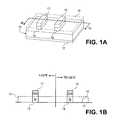
- FIG. 1Ais a perspective view of a substrate which includes two silicon bodies with overlying insulative members
- FIG. 1Bis a cross-sectional view of the structure of FIG. 1 taken through section line 1 B- 1 B of FIG. 1A .
- FIG. 2Aillustrates the structure of FIG. 1 following deposition of a sacrificial layer.
- FIG. 2Billustrates the structure of FIG. 2A following planarization of the sacrificial layer.
- FIG. 2Cillustrates the structure of FIG. 2B following deposition of a hardmask layer over the planarized sacrificial layer.
- FIG. 2Dillustrates a perspective view of the structure of FIG. 1 following the patterning of the hardmask and sacrificial layers.
- FIG. 2Eis a cross-sectional view of the structure of FIG. 2D taken through section line 2 E- 2 E of FIG. 2D .
- FIG. 3is a perspective view of the structure of FIG. 2D following the deposition of an interlayer dielectric (ILD).
- ILDinterlayer dielectric
- FIG. 4Ais a perspective view of the structure of FIG. 3 following planarization of the ILD to a point where it exposes remaining portions of the insulative members 17 and 18 .
- FIG. 4Bis a cross-sectional view taken through section line 4 B- 4 B of FIG. 4A .
- FIG. 5is a perspective view of the structure of FIG. 4 following the covering of a section of the substrate on which an I-gate transistor is fabricated.
- FIG. 6Ais a perspective view of the structure of FIG. 5 following an etching step.
- FIG. 6Bis a cross-sectional view of the structure of FIG. 6A taken through section line 6 B- 6 B of FIG. 6A .
- FIG. 7Ais a perspective view of the structure of FIG. 6A following removal of the patterned, sacrificial layer and formation of trench opening in the ILD.
- FIG. 7Bis a cross-sectional view of the structure of FIG. 7A taken through section line 7 B- 7 B of FIG. 7A .
- FIG. 8is a cross-sectional view of the structure of FIG. 7B following the formation of an insulative layer and a gate layer in the trench opening.
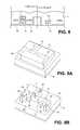
- FIG. 9Ais a perspective view of the structure of FIG. 8 following planarization of the gate layer.
- FIG. 9Bis a perspective view of the structure of FIG. 9A with the ILD removed.
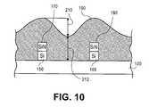
- FIG. 10is a cross-sectional view showing topography variations that can be encountered when forming gate-defining members using conventional processing.
- the method which followsdescribes the formation of both the I-gate transistor and a tri-gate transistor in a single process flow. While the fabrication of only a single I-gate transistor and a single tri-gate transistor are illustrated, it will be apparent to one skilled in the art, that in a typical integrated circuit, numerous such transistors are simultaneously fabricated. Moreover, the I-gate and tri-gate transistors may be fabricated wherever needed in the integrated circuit. Thus, a single circuit, such as a buffer, may have both I-gate and tri-gate transistors. In some cases, for example in a DRAM, an array of memory cells using only I-gate transistors may be fabricated and connected to peripheral circuits which use both I-gate and tri-gate transistors. A memory using I-gate memory cells is described in “Memory with Split-Gate Devices and Method of Fabrication,” Ser. No. 10/816,282, filed Mar. 31, 2004, and assigned to the assignee of the present application.
- the transistorsare fabricated on an oxide layer 10 which is formed on a semiconductor substrate, for example a silicon substrate 12 .
- the transistor bodiesare fabricated from a monocrystalline silicon layer 14 (shown in dotted lines in FIGS. 1A and 1B ) disposed on layer 10 .
- This silicon-on-insulator (SOI) substrateis well-known in the semiconductor industry, where as shown, the layer 14 is disposed on the layer 10 .
- the SOI substrateis fabricated by bonding the oxide layer 10 and a silicon layer 14 onto the substrate 12 , and then, planarizing the layer 14 so that it is relatively thin. This relatively thin, low body effect layer, is used to form the bodies of active devices, as mentioned.
- an SOI substrateincluding, for instance, the implantation of oxygen into a silicon substrate to form a buried oxide layer.
- the transistorsare shown fabricated on the oxide layer 10 , the underlying silicon substrate 12 is not shown.
- the layer 14may be selectively ion-implanted with an n-type dopant in the regions where n channel devices are to be fabricated, and with a p type dopant in those regions where p channel devices are to be fabricated. This is used to provide the relatively light doping typically found in the channel regions of MOS devices fabricated in a CMOS integrated circuit.
- Both the I-gate and tri-gate transistorsmay be fabricated with the described process as either p channel or n channel devices. (The doping of the channel regions of the transistors may be done at other points in the process flow such as the point in the process shown in FIG. 1A or 7 A.)
- a protective oxide(not shown) is disposed on the silicon layer 14 followed by the deposition of a silicon nitride layer.
- the nitride layeris masked to define a plurality of insulative members, such as members 17 and 18 of FIGS. 1A and 1B .
- the underlying silicon layer 14is etched in alignment with these members resulting in the silicon bodies 15 and 16 .
- the width of the silicon bodies 15 and 16may be the critical dimension in a particular process, for instance, in a 30 nanometer (nm) gate length process, these bodies may have a width of 30 nm.
- the thickness of the layer 14 , and the silicon nitride layer from which the members 17 and 18 are formed,may each be, by way of example, in the range of 10-100 nm.
- a sacrificial layer 19is deposited over the stacks (i.e. the insulative members/silicon bodies 17 / 15 and 18 / 16 ) and on the oxide layer 10 .
- this layeris a polysilicon layer 50-200 nm thick.
- other materialsmay be used for the sacrificial layer 19 .
- the material used for the sacrificial layer 19should be able to protect the channel regions of the devices from ion implantation during the formation of the source and drain regions, as will be described.
- the sacrificial layershould be selectively removable so as not to significantly impact the integrity of an ILD formed around the sacrificial layer after patterning to form sacrificial gate members, as will be described.
- the insulative members, such as for example member 18should be able to be selectively removed in the presence of the sacrificial layer, so as to facilitate formation of the tri-gate transistor.
- the sacrificial layer 19is planarized prior to patterning and etching the sacrificial gate-defining members. To the extent that the sacrificial layer 19 is not planar, gate patterning issues, such as those discussed with respect to FIG. 10 , can be encountered.
- a sacrificial layer 190such as a sacrificial polysilicon layer, is deposited over the stacks.
- the sacrificial layer 190is deposited so that it completely covers the stacks.
- the sacrificial layer 190is subsequently patterned and etched to form sacrificial gate-defining members.
- the gate-defining memberstemporarily occupy regions where gates for the I-gate and tri-gate transistors are eventually formed.
- the gate-defining memberscan also be used to facilitate selective removal the insulative member 180 during formation of the tri-gate transistor.
- forming the sacrificial layer so that it completely covers the stackscan result in the formation of large topography non-uniformities 210 .
- These non-uniformitiescan create difficulties when patterning resist features that define the sacrificial gate-defining members.
- the degree of the non-uniformity 210depends on the distance between underlying features and the thickness of the sacrificial layer (i.e., underlying features that are in closer to each other can have less topography associated with them than features that are spaced farther apart), variations can exist in the thickness 212 of the sacrificial layer.
- These thickness variationscan affect the quality of the etch process used to define the gate-defining members and result in underetch in some regions and overetch in other regions.
- the topographyimpacts photolithography and/or causes underetch or overetch of the sacrificial polysilicon layer, it can result in the manifestation of defects in the permanent gate structures. These defects can thereby impact the yield, functionality, and reliability of resulting transistors.
- One embodiment of the present inventionovercomes these limitations by first planarizing the sacrificial polysilicon layer, and thereby eliminating the topography and its associated variations, prior to patterning, etching, and forming the sacrificial gate-defining members. More specifically after depositing the sacrificial layer 19 , as shown in FIG. 2A .
- the sacrificial layer 19is planarized as shown in FIG. 2B . Planarization can be accomplished using a conventional chemical mechanical polishing (CMP) process, a reactive ion etch process, or the like.
- CMPchemical mechanical polishing
- the CMP processcan be a timed polish or the insulative members 17 and 18 can function as polish stops whereupon exposure of the upper surfaces of the insulative members 17 and 18 , the CMP system responds by terminating the polishing process immediately, terminating after a predetermined time, or terminating after performing an overpolish processing step. While the cross-sectional view shown in FIG. 2B shows that the planarization process produces surfaces of the sacrificial polysilicon layer 19 and insulative members 17 / 18 that are co-planar, one of ordinary skill appreciates that the polish or etch back process could alternatively terminate at some point prior to exposing the insulating members 17 and 18 .
- planarized sacrificial layernow has a more planar topography as compared to the conventional process, thereby facilitating the patterning and etching of the gate-defining members.
- resulting etched featureswill have reduced aspect ratios, as compared to conventionally used process flows, thereby facilitating improved step coverage of subsequently deposited films.
- an optional hardmask layer 21can now be formed over the planarized sacrificial layer 19 .
- the hardmask layeris a silicon oxynitride layer.
- the hardmask layercan include other materials such as silicon nitride, silicon-rich-silicon-nitride, or the like.
- the hardmask layerprovides a uniform surface onto which the resist can be patterned, i.e., instead of the exposed surface area including areas of SiN (insulative members 17 and 18 ) and areas of polysilicon (sacrificial layer 19 ), the hardmask provides a single surface (e.g., oxide) onto which the resist is patterned. This can reduce resist adhesion problems.
- the hardmask layershould have a thickness that sufficiently protects the sacrificial layer during the subsequent etch process to define the gate-defining members.
- the sacrificial and hardmask layersare patterned and etched. As a result, remaining portions of the sacrificial layer 19 thereby form gate-defining members shown as members 20 and 22 in FIGS. 2D and 2E .
- the member 20occupies the region in which the two gates for the I-gate transistor is fabricated as well as areas where contact and/or via connections can be made.
- the member 22occupies the region in which the tri-gate is formed for the tri-gate transistor, as well as an area, again for contacts and/or vias.
- the sacrificial layer etch to form the gate-defining membersis less prone to problems with underetch and overetch. This not only reduces the occurrence of overetch and underetch related defects, it can also reduce cycle time and improve the overall manufacturability of the sacrificial layer etch process.
- portions of the insulative members 17 and 18 not covered by the gate-defining members 20 and 22may be etched, thereby exposing portions of the underlying silicon bodies 15 and 16 .
- the silicon bodies 15 and 16to the extent they are not covered by the members 20 and 22 , can be ion implanted to form source and drain regions for both the I-gate and tri-gate transistors.
- separate ion implantation stepsare used for the p channel and n channel devices, with protective layers or masking layer being used to permit separate implantation of the source and drains for the p channel and n channel devices.
- spacers 23may be formed to allow a more lightly doped source and drain region to be implanted adjacent the channel region, and more heavily doped source and drain regions spaced apart from the channel region. This is described in the above-referenced application Ser. No. 10/816,282.
- an ILD 30is now formed over the insulative layer 10 , gate-defining members 20 and 22 , and silicon bodies 15 and 16 .
- the ILD 30is formed adjacent the sides of the members 20 and 22 , and as will be seen, is used to form a trench that allows the inlay of metal once the gate-defining members are removed.
- the ILD 30may be, for instance, a chemical vapor deposited (CVD) silicon dioxide layer.
- the ILD 30is then planarized, for instance, using a CMP process, so as to remove portions of the ILD 30 and portions of the hardmask 21 overlying insulative members 17 and 18 , thereby exposing the upper surfaces of the insulative members 17 and 18 .
- Thisis illustrated in both FIGS. 4A and 4B . Note, the upper surfaces of members 17 and 18 are flush with the upper surface of the ILD 30 and the upper surfaces of the members 20 and 22 .
- a masking layer(photoresist mask layer and/or an oxide hardmask layer) is deposited over the structure of FIGS. 4A and 4B , and patterned so as to remain in place over the I-gate transistor region.
- the masking layer 50covers the insulative member 17 . As shown in FIG. 5 , the masking layer 50 leaves exposed insulative member 18 of the tri-gate device.
- an etching processis used to remove the plug-shaped silicon nitride member 18 .
- An etchantthat discriminates between the silicon nitride and both the ILD 30 and sacrificial layer is used so that the ILD 30 and member 22 remain substantially intact.
- a dry or wet etchantmay be used.
- a conventional hot phosphoric acid bathis used to remove the silicon nitride member 18 .
- the polysilicon sacrificial layeris next removed with, for example, a wet etch process.
- the resultant structureis shown in FIGS. 7A and 7B .
- the remaining ILD 30now defines a trench formed in a pattern in which the gates for the transistors are to be fabricated.
- a gate dielectric layer 60is formed on and around each semiconductor bodies 15 and 16 as seen in FIG. 8 .
- a gate dielectricmay be deposited such that it covers the top surface of the semiconductor body 16 and the insulative member 17 as well as on the opposite side-walls of each of the semiconductor bodies.
- This gate dielectricideally has a high dielectric constant, such as a metal oxide dielectric, for instance, HfO 2 or ZrO or other high-k dielectrics, such as PZT or BST.
- a high-k dielectric filmcan be formed by any well-known technique such as by chemical vapor deposition (CVD), atomic layer deposition (ALD), or the like.
- the gate dielectriccan be a grown dielectric.
- the gate dielectric layer 60is a silicon dioxide film grown with a dry/wet oxidation process.
- the silicon dioxide filmis grown to a thickness of between 5-50 ⁇ .
- a conformally deposited dielectric layeris shown in FIG. 8 .
- a gate electrode (metal) layer 61is formed over the gate dielectric layer 60 .
- the gate electrode layer 61may be formed by blanket deposition of a suitable gate electrode material.
- a gate electrode materialcomprises a metal film such as Tungsten, Tantalum, Titanium and/or nitrides and alloys thereof.
- a work function in the range of 4.0 to 4.6 eVmay be used.
- a work function of 4.6 to 5.2 eVmay be used. Consequently, for substrates with both n channel and p channel transistors, two separate metal deposition processes may need to be used.
- the metal layer 61is planarized using, for example CMP, and such planarization continues until at least the upper surface of the insulative member 17 is exposed, as shown in FIGS. 9A and 9B . This is done in order to assure that no metal spans the member 17 , since otherwise, the gates in the I-gate transistor will be shorted together. As can be seen in FIG. 9 , there are two independent gates 62 and 64 for the I-gate transistor, and a single gate 65 for the tri-gate device.
- the gate 65 for the tri-gate transistorhas a top surface opposite the bottom surface and has a pair of laterally opposite sidewalls formed adjacent the tri-gate structure best seen in FIG. 9B . These sidewalls are connected on the upper surface of the silicon body. Thus, the gate surrounds the channel region of the tri-gate transistor on three sides.
- two independent gates 62 and 64are separated by the insulative member 17 , again best seen in FIG. 9B (where the ILD is shown removed).
- the silicon bodies 15 and 16are shown on the insulative layer 10 .
- Source regions 68 and 70are shown for each of the transistors along with drain regions 71 and 72 .
- the independent gates 62 and 64along with their orthogonally disposed contact areas are readily seen. The same is true for the gate 65 . These areas allow for easier contact to be made to the gates from overlying conductive structures, as shown by contact regions 80 , 81 and 82 . While not shown in FIG. 9B , contact can be made to the source and drain regions as well as to the gates from overlying metallization layers through contacts and or vias (not shown).
- I-gate transistorsmay be used in logic circuits along with the tri-gate transistors. I-gate transistors have characteristics which make them desirable in certain circuits. For instance, a single I-gate transistor may provide both a high current and medium current device depending on the potential applied to one or both gates. Such devices may provide a “strong off” device to reduce leakage in a sleep mode or power-down mode. I-gate transistors also provide a device for pre-charge lines by allowing a trickle current. In the above-mentioned patent application, the I-gate devices can be used as DRAM cells, and the process described above, may be used in connection with such DRAM fabrication. In this case, the silicon body 15 is an elongated body formed in a plurality of parallel, spaced-apart lines and used in an array of DRAM cells.
- dielectric material in trench isolation structures formed in a bulk monocrystalline silicon substratecan be recessed to form raised channel regions (similar to members 15 and 16 in FIG. 2A ), and thereafter a sacrificial layer (similar to sacrificial layer 19 in FIG. 2A ) can be deposited over the raised channel regions and planarized as shown in FIG. 2B .
- a sacrificial layersimilar to sacrificial layer 19 in FIG. 2A
- topography variations that can impact the patterning and etch processes that define sacrificial gate-defining memberscan be reduced.
Landscapes
- Engineering & Computer Science (AREA)
- Manufacturing & Machinery (AREA)
- Metal-Oxide And Bipolar Metal-Oxide Semiconductor Integrated Circuits (AREA)
- Thin Film Transistor (AREA)
- Insulated Gate Type Field-Effect Transistor (AREA)
- Semiconductor Memories (AREA)
- Non-Volatile Memory (AREA)
Abstract
Description
- This is a Continuation of application Ser. No. 11/355,103, Filed Jan. 18, 2006 which is a Divisional of application Ser. No. 11/142,572 filed May 4, 2005, which is a Continuation-in Part of application Ser. No. 10/955,670 filed Sep. 29, 2004 which are presently pending.
- This patent application is a continuation-in-part of U.S. patent application Ser. No. 10/955,670, filed Sep. 29, 2004, entitled INDEPENDENTLY-ACCESSED DOUBLE-GATE AND TRI-GATE TRANSISTORS IN SAME PROCESS FLOW, by Brian S. Doyle.
- The invention relates to the field of semiconductor processing.
- Independently-controlled double-gate (I-gate) transistors are a relatively recent development in semiconductor processing. They have two gates disposed on opposite sides of a channel, each gate capable of being independently controlled. This provides added transistor flexibility and enables, for example, using a single body to form a dynamic random-access memory (DRAM) cell. Tri-gate transistors are another relatively recent development in semiconductor processing. With tri-gate transistors, the gate forms adjacent three sides of a channel region. Tri-gate transistors, particularly when used with a high-k insulator and metal gate, can substantially improve the speed and performance of integrated circuits.
- A number of I-gate structures have been proposed. This and other related technology is described at C. Kuo,IEDM, December 2002, following M. Chan Electron Device Letters, January 1994; C. Kuo,IEDM, December 2002, “A Hypothetical Construction of the Double Gate Floating Body Cell;” T. Ohsawa, et al.,IEEE Journal of Solid-State Circuits, Vol. 37, No. 11, November 2002; David M. Fried, et al., “High-Performance P-Type Independent-Gate FinFETs,”IEEE Electron Device Letters, Vol. 25, No. 4, April 2004; and David M. Fried, et al., “Improved Independent Gate N-Type FinFET Fabrication and Characterization,”IEEE Electron Device Letters, Vol. 24, No. 9, September 2003. Tri-gate structures are described at, for instance, publication number U.S. 2004-0036127-A1.
FIG. 1A is a perspective view of a substrate which includes two silicon bodies with overlying insulative membersFIG. 1B is a cross-sectional view of the structure ofFIG. 1 taken throughsection line 1B-1B ofFIG. 1A .FIG. 2A illustrates the structure ofFIG. 1 following deposition of a sacrificial layer.FIG. 2B illustrates the structure ofFIG. 2A following planarization of the sacrificial layer.FIG. 2C illustrates the structure ofFIG. 2B following deposition of a hardmask layer over the planarized sacrificial layer.FIG. 2D illustrates a perspective view of the structure ofFIG. 1 following the patterning of the hardmask and sacrificial layers.FIG. 2E is a cross-sectional view of the structure ofFIG. 2D taken throughsection line 2E-2E ofFIG. 2D .FIG. 3 is a perspective view of the structure ofFIG. 2D following the deposition of an interlayer dielectric (ILD).FIG. 4A is a perspective view of the structure ofFIG. 3 following planarization of the ILD to a point where it exposes remaining portions of theinsulative members FIG. 4B is a cross-sectional view taken throughsection line 4B-4B ofFIG. 4A .FIG. 5 is a perspective view of the structure ofFIG. 4 following the covering of a section of the substrate on which an I-gate transistor is fabricated.FIG. 6A is a perspective view of the structure ofFIG. 5 following an etching step.FIG. 6B is a cross-sectional view of the structure ofFIG. 6A taken throughsection line 6B-6B ofFIG. 6A .FIG. 7A is a perspective view of the structure ofFIG. 6A following removal of the patterned, sacrificial layer and formation of trench opening in the ILD.FIG. 7B is a cross-sectional view of the structure ofFIG. 7A taken throughsection line 7B-7B ofFIG. 7A .FIG. 8 is a cross-sectional view of the structure ofFIG. 7B following the formation of an insulative layer and a gate layer in the trench opening.FIG. 9A is a perspective view of the structure ofFIG. 8 following planarization of the gate layer.FIG. 9B is a perspective view of the structure ofFIG. 9A with the ILD removed.FIG. 10 is a cross-sectional view showing topography variations that can be encountered when forming gate-defining members using conventional processing.- In the following description, the fabricating of an independently accessed, double-gate (I-gate) transistor and a tri-gate transistor on a common substrate is described. Numerous specific details are set forth, such as specific materials, in order to provide a thorough understanding of the present invention. It will be apparent to one skilled in the art, that the present invention may be practiced without these specific details. In other instances, well known processing steps have not been described in detail, in order not to unnecessarily obscure the present invention. For example, well-known cleaning steps, and some protective layers often used in the fabrication of integrated circuits, are not described.
- The method which follows describes the formation of both the I-gate transistor and a tri-gate transistor in a single process flow. While the fabrication of only a single I-gate transistor and a single tri-gate transistor are illustrated, it will be apparent to one skilled in the art, that in a typical integrated circuit, numerous such transistors are simultaneously fabricated. Moreover, the I-gate and tri-gate transistors may be fabricated wherever needed in the integrated circuit. Thus, a single circuit, such as a buffer, may have both I-gate and tri-gate transistors. In some cases, for example in a DRAM, an array of memory cells using only I-gate transistors may be fabricated and connected to peripheral circuits which use both I-gate and tri-gate transistors. A memory using I-gate memory cells is described in “Memory with Split-Gate Devices and Method of Fabrication,” Ser. No. 10/816,282, filed Mar. 31, 2004, and assigned to the assignee of the present application.
- In one embodiment, the transistors are fabricated on an
oxide layer 10 which is formed on a semiconductor substrate, for example asilicon substrate 12. The transistor bodies are fabricated from a monocrystalline silicon layer14 (shown in dotted lines inFIGS. 1A and 1B ) disposed onlayer 10. This silicon-on-insulator (SOI) substrate is well-known in the semiconductor industry, where as shown, thelayer 14 is disposed on thelayer 10. By way of example, the SOI substrate is fabricated by bonding theoxide layer 10 and asilicon layer 14 onto thesubstrate 12, and then, planarizing thelayer 14 so that it is relatively thin. This relatively thin, low body effect layer, is used to form the bodies of active devices, as mentioned. Other techniques are known for forming an SOI substrate including, for instance, the implantation of oxygen into a silicon substrate to form a buried oxide layer. In the subsequent cross-sectional views, the transistors are shown fabricated on theoxide layer 10, theunderlying silicon substrate 12 is not shown. - The
layer 14 may be selectively ion-implanted with an n-type dopant in the regions where n channel devices are to be fabricated, and with a p type dopant in those regions where p channel devices are to be fabricated. This is used to provide the relatively light doping typically found in the channel regions of MOS devices fabricated in a CMOS integrated circuit. Both the I-gate and tri-gate transistors may be fabricated with the described process as either p channel or n channel devices. (The doping of the channel regions of the transistors may be done at other points in the process flow such as the point in the process shown inFIG. 1A or7A.) - In the processing for one embodiment, a protective oxide (not shown) is disposed on the
silicon layer 14 followed by the deposition of a silicon nitride layer. The nitride layer is masked to define a plurality of insulative members, such asmembers FIGS. 1A and 1B . Then, theunderlying silicon layer 14 is etched in alignment with these members resulting in thesilicon bodies - The width of the
silicon bodies layer 14, and the silicon nitride layer from which themembers - Next as shown in
FIG. 2A , asacrificial layer 19 is deposited over the stacks (i.e. the insulative members/silicon bodies 17/15 and18/16) and on theoxide layer 10. In one embodiment, this layer is a polysilicon layer 50-200 nm thick. However, other materials may be used for thesacrificial layer 19. The material used for thesacrificial layer 19 should be able to protect the channel regions of the devices from ion implantation during the formation of the source and drain regions, as will be described. And, the sacrificial layer should be selectively removable so as not to significantly impact the integrity of an ILD formed around the sacrificial layer after patterning to form sacrificial gate members, as will be described. Additionally, the insulative members, such as forexample member 18 should be able to be selectively removed in the presence of the sacrificial layer, so as to facilitate formation of the tri-gate transistor. - In accordance with one embodiment, unlike conventional methods, the
sacrificial layer 19 is planarized prior to patterning and etching the sacrificial gate-defining members. To the extent that thesacrificial layer 19 is not planar, gate patterning issues, such as those discussed with respect toFIG. 10 , can be encountered. - As shown in
FIG. 10 , after the silicon nitride (SiN) layer and underlying silicon layer are patterned and etched to the form stacks that include insulative members/silicon bodies 170/150 and180/160 (similar tostacks 17/15 and18/16 inFIGS. 1A and 1B ), asacrificial layer 190, such as a sacrificial polysilicon layer, is deposited over the stacks. Thesacrificial layer 190 is deposited so that it completely covers the stacks. Thesacrificial layer 190 is subsequently patterned and etched to form sacrificial gate-defining members. The gate-defining members temporarily occupy regions where gates for the I-gate and tri-gate transistors are eventually formed. The gate-defining members can also be used to facilitate selective removal theinsulative member 180 during formation of the tri-gate transistor. - However, as shown in
FIG. 10 , forming the sacrificial layer so that it completely covers the stacks can result in the formation oflarge topography non-uniformities 210. These non-uniformities can create difficulties when patterning resist features that define the sacrificial gate-defining members. In addition, as one of ordinary skill can appreciate, because the degree of the non-uniformity210 depends on the distance between underlying features and the thickness of the sacrificial layer (i.e., underlying features that are in closer to each other can have less topography associated with them than features that are spaced farther apart), variations can exist in thethickness 212 of the sacrificial layer. These thickness variations can affect the quality of the etch process used to define the gate-defining members and result in underetch in some regions and overetch in other regions. To the extent that the topography impacts photolithography and/or causes underetch or overetch of the sacrificial polysilicon layer, it can result in the manifestation of defects in the permanent gate structures. These defects can thereby impact the yield, functionality, and reliability of resulting transistors. - One embodiment of the present invention overcomes these limitations by first planarizing the sacrificial polysilicon layer, and thereby eliminating the topography and its associated variations, prior to patterning, etching, and forming the sacrificial gate-defining members. More specifically after depositing the
sacrificial layer 19, as shown inFIG. 2A . Thesacrificial layer 19 is planarized as shown inFIG. 2B . Planarization can be accomplished using a conventional chemical mechanical polishing (CMP) process, a reactive ion etch process, or the like. In embodiments where a CMP process is used, the CMP process can be a timed polish or theinsulative members insulative members FIG. 2B shows that the planarization process produces surfaces of thesacrificial polysilicon layer 19 andinsulative members 17/18 that are co-planar, one of ordinary skill appreciates that the polish or etch back process could alternatively terminate at some point prior to exposing the insulatingmembers - As shown in
FIG. 2C , anoptional hardmask layer 21 can now be formed over the planarizedsacrificial layer 19. In one embodiment, the hardmask layer is a silicon oxynitride layer. Alternatively, the hardmask layer can include other materials such as silicon nitride, silicon-rich-silicon-nitride, or the like. The hardmask layer provides a uniform surface onto which the resist can be patterned, i.e., instead of the exposed surface area including areas of SiN (insulative members 17 and18) and areas of polysilicon (sacrificial layer19), the hardmask provides a single surface (e.g., oxide) onto which the resist is patterned. This can reduce resist adhesion problems. In addition, it functions as a protective masking layer during subsequent etch processes to define the gate-defining members and thereby allows the use of thinner resists so that increasingly smaller feature sizes can be patterned. Therefore, the hardmask layer should have a thickness that sufficiently protects the sacrificial layer during the subsequent etch process to define the gate-defining members. - Next, the sacrificial and hardmask layers are patterned and etched. As a result, remaining portions of the
sacrificial layer 19 thereby form gate-defining members shown asmembers FIGS. 2D and 2E . Themember 20 occupies the region in which the two gates for the I-gate transistor is fabricated as well as areas where contact and/or via connections can be made. Themember 22 occupies the region in which the tri-gate is formed for the tri-gate transistor, as well as an area, again for contacts and/or vias. Because thesacrificial layer 19 is now thinner than it otherwise would be using conventional methods and because its topography has much less variation associated with it, the sacrificial layer etch to form the gate-defining members is less prone to problems with underetch and overetch. This not only reduces the occurrence of overetch and underetch related defects, it can also reduce cycle time and improve the overall manufacturability of the sacrificial layer etch process. - Also, as shown in
FIG. 2D , at this point in the process, portions of theinsulative members members underlying silicon bodies arrows 25, thesilicon bodies members - Additionally, spacers23 may be formed to allow a more lightly doped source and drain region to be implanted adjacent the channel region, and more heavily doped source and drain regions spaced apart from the channel region. This is described in the above-referenced application Ser. No. 10/816,282.
- Turning now to
FIG. 3 , anILD 30 is now formed over theinsulative layer 10, gate-definingmembers silicon bodies ILD 30 is formed adjacent the sides of themembers ILD 30 may be, for instance, a chemical vapor deposited (CVD) silicon dioxide layer. - The
ILD 30 is then planarized, for instance, using a CMP process, so as to remove portions of theILD 30 and portions of thehardmask 21overlying insulative members insulative members FIGS. 4A and 4B . Note, the upper surfaces ofmembers ILD 30 and the upper surfaces of themembers - Now, a masking layer (photoresist mask layer and/or an oxide hardmask layer) is deposited over the structure of
FIGS. 4A and 4B , and patterned so as to remain in place over the I-gate transistor region. Themasking layer 50 covers the insulativemember 17. As shown inFIG. 5 , themasking layer 50 leaves exposedinsulative member 18 of the tri-gate device. - Then, as shown in
FIGS. 6A and 6B , an etching process is used to remove the plug-shapedsilicon nitride member 18. An etchant that discriminates between the silicon nitride and both theILD 30 and sacrificial layer is used so that theILD 30 andmember 22 remain substantially intact. A dry or wet etchant may be used. In one embodiment, a conventional hot phosphoric acid bath is used to remove thesilicon nitride member 18. In this embodiment, it may be advantageous to use an oxide hardmask as themasking layer 50. Once themember 18 is removed, theunderlying silicon body 16 as shown inFIG. 6B is exposed. - The polysilicon sacrificial layer is next removed with, for example, a wet etch process. The resultant structure is shown in
FIGS. 7A and 7B . The remainingILD 30 now defines a trench formed in a pattern in which the gates for the transistors are to be fabricated. - A
gate dielectric layer 60 is formed on and around eachsemiconductor bodies FIG. 8 . Specifically, a gate dielectric may be deposited such that it covers the top surface of thesemiconductor body 16 and theinsulative member 17 as well as on the opposite side-walls of each of the semiconductor bodies. This gate dielectric ideally has a high dielectric constant, such as a metal oxide dielectric, for instance, HfO2or ZrO or other high-k dielectrics, such as PZT or BST. A high-k dielectric film can be formed by any well-known technique such as by chemical vapor deposition (CVD), atomic layer deposition (ALD), or the like. Alternatively, the gate dielectric can be a grown dielectric. In one embodiment, thegate dielectric layer 60 is a silicon dioxide film grown with a dry/wet oxidation process. For example, the silicon dioxide film is grown to a thickness of between 5-50 Å. (A conformally deposited dielectric layer is shown inFIG. 8 .) - Next, as shown in
FIG. 8 , a gate electrode (metal)layer 61 is formed over thegate dielectric layer 60. Thegate electrode layer 61 may be formed by blanket deposition of a suitable gate electrode material. In one embodiment, a gate electrode material comprises a metal film such as Tungsten, Tantalum, Titanium and/or nitrides and alloys thereof. For the n channel, I-gate and tri-gate transistors, a work function in the range of 4.0 to 4.6 eV may be used. For the p channel, I-gate and tri-gate transistors, a work function of 4.6 to 5.2 eV may be used. Consequently, for substrates with both n channel and p channel transistors, two separate metal deposition processes may need to be used. - The
metal layer 61 is planarized using, for example CMP, and such planarization continues until at least the upper surface of theinsulative member 17 is exposed, as shown inFIGS. 9A and 9B . This is done in order to assure that no metal spans themember 17, since otherwise, the gates in the I-gate transistor will be shorted together. As can be seen inFIG. 9 , there are twoindependent gates single gate 65 for the tri-gate device. - The
gate 65 for the tri-gate transistor has a top surface opposite the bottom surface and has a pair of laterally opposite sidewalls formed adjacent the tri-gate structure best seen inFIG. 9B . These sidewalls are connected on the upper surface of the silicon body. Thus, the gate surrounds the channel region of the tri-gate transistor on three sides. For the I-gate transistor, twoindependent gates member 17, again best seen inFIG. 9B (where the ILD is shown removed). - Also, best seen in
FIG. 9B , thesilicon bodies insulative layer 10.Source regions drain regions independent gates gate 65. These areas allow for easier contact to be made to the gates from overlying conductive structures, as shown bycontact regions FIG. 9B , contact can be made to the source and drain regions as well as to the gates from overlying metallization layers through contacts and or vias (not shown). - I-gate transistors may be used in logic circuits along with the tri-gate transistors. I-gate transistors have characteristics which make them desirable in certain circuits. For instance, a single I-gate transistor may provide both a high current and medium current device depending on the potential applied to one or both gates. Such devices may provide a “strong off” device to reduce leakage in a sleep mode or power-down mode. I-gate transistors also provide a device for pre-charge lines by allowing a trickle current. In the above-mentioned patent application, the I-gate devices can be used as DRAM cells, and the process described above, may be used in connection with such DRAM fabrication. In this case, the
silicon body 15 is an elongated body formed in a plurality of parallel, spaced-apart lines and used in an array of DRAM cells. - While in the figures two separate silicon bodies are shown, it will be appreciated that a single body may be used. Then, a tri-gate and I-gate transistor may be fabricated in series with one another. In addition, one of ordinary skill appreciates that while in the foregoing discussion silicon is used as the semiconductor material to form the silicon bodies, the bodies can alternatively comprise other semiconductor materials in addition to or instead of silicon. Also, while embodiments of the present invention have been described in conjunction with the formation of transistors using an SOI substrate, one of ordinary skill appreciates that one or more of these embodiments can be incorporated into processes that form I-Gate/Tri-gate transistors in a bulk monocrystalline substrate, For example, dielectric material in trench isolation structures formed in a bulk monocrystalline silicon substrate can be recessed to form raised channel regions (similar to
members FIG. 2A ), and thereafter a sacrificial layer (similar tosacrificial layer 19 inFIG. 2A ) can be deposited over the raised channel regions and planarized as shown inFIG. 2B . In this way, topography variations that can impact the patterning and etch processes that define sacrificial gate-defining members can be reduced. - Thus, a process has been described and a resultant structure for an integrated circuit having both an I-gate and tri-gate structure on a common substrate.
Claims (20)
1. A method comprising:
forming a first transistor on a substrate having a first body surrounded on three sides by a first metal gate; and
forming a second transistor on the substrate having a second body having two independent metal gates on opposite sides of the second body, and an insulative member formed on the second body, the insulative member formed between the two independent metal gates, wherein the first and second transistors are formed in a same process flow.
2. The method ofclaim 1 wherein same process steps are used to form the bodies, the metal gates, and gate dielectrics of the two transistors.
3. The method ofclaim 1 wherein a same process step is used to form spacer of the two transistors.
4. The method ofclaim 1 wherein a same process step is used to form gate contacts of the two transistors.
5. The method ofclaim 1 further comprising:
forming two insulative members on the first and second bodies using a same process step;
shielding the second transistor to remove the first insulative member.
6. A method comprising:
forming at least two semiconductor bodies from a semiconductor layer;
forming an insulative member on the second semiconductor body;
patterning a dielectric layer to form two gate dielectric layers on the two semiconductor bodies; and
forming a conductive layer to form a first metal gate surrounding on three sides of the first semiconductor body and two independent metal gates on opposite sides of the second semiconductor body, the insulative member formed between the two independent metal gates, wherein the semiconductor bodies, the gate dielectric layers and the metal gates are formed in a same process step.
7. The method ofclaim 6 , further comprising patterning a sacrificial layer to form sacrificial gates for the two semiconductor bodies.
8. The method ofclaim 6 , further comprising planarizing the sacrificial layer before patterning.
9. The method ofclaim 6 , further comprising forming a hardmask layer over the sacrificial layer after planarizing.
10. The method ofclaim 6 , wherein planarizing is further characterized as using an etch-back process to planarize the surface of the sacrificial layer.
11. The method ofclaim 6 , further comprising removing the sacrificial gates before forming the metal gates.
12. The method ofclaim 6 , further comprising patterning a spacer layer to form spacers for the two semiconductor bodies.
13. The method ofclaim 6 , wherein forming an insulative member on one semiconductor body comprises patterning an insulative layer to form two insulative members overlying the two semiconductor bodies;
removing an insulative member on the first semiconductor body.
14. The method ofclaim 13 , further comprising enclosing sacrificial gates and the semiconductor bodies with the overlying insulative members in a dielectric layer.
15. The method ofclaim 14 , further comprising planarizing the dielectric layer to expose portions of the insulative members before removing an insulative member.
16. An integrated circuit formed by a process that includes:
forming a first transistor on a substrate having a first body surrounded on three sides by a first metal gate; and
forming a second transistor on the substrate having a second body having two independent metal gates on opposite sides of the second body, and an insulative member formed on the second body, the insulative member is formed between the two independent metal gates,
wherein the first and second transistors are formed in a same process flow.
17. The integrated circuit ofclaim 16 , wherein the semiconductor bodies comprise monocrystalline silicon.
18. The integrated circuit ofclaim 16 , wherein the insulative member comprises silicon nitride.
19. The integrated circuit ofclaim 16 , wherein the first and second gate dielectrics are made of a high dielectric constant material selected from the group consisting of metal oxides, PZT or BST.
20. The integrated circuit ofclaim 16 , wherein the first, second and third gate electrodes are made of a material selected from the group consisting of tungsten, tantalum and titanium.
Priority Applications (2)
| Application Number | Priority Date | Filing Date | Title |
|---|---|---|---|
| US12/852,408US8268709B2 (en) | 2004-09-29 | 2010-08-06 | Independently accessed double-gate and tri-gate transistors in same process flow |
| US13/620,282US8399922B2 (en) | 2004-09-29 | 2012-09-14 | Independently accessed double-gate and tri-gate transistors |
Applications Claiming Priority (4)
| Application Number | Priority Date | Filing Date | Title |
|---|---|---|---|
| US10/955,670US7422946B2 (en) | 2004-09-29 | 2004-09-29 | Independently accessed double-gate and tri-gate transistors in same process flow |
| US11/124,572US7037790B2 (en) | 2004-09-29 | 2005-05-04 | Independently accessed double-gate and tri-gate transistors in same process flow |
| US11/335,103US7859053B2 (en) | 2004-09-29 | 2006-01-18 | Independently accessed double-gate and tri-gate transistors in same process flow |
| US12/852,408US8268709B2 (en) | 2004-09-29 | 2010-08-06 | Independently accessed double-gate and tri-gate transistors in same process flow |
Related Parent Applications (2)
| Application Number | Title | Priority Date | Filing Date |
|---|---|---|---|
| US11/335,103ContinuationUS7859053B2 (en) | 2004-09-29 | 2006-01-18 | Independently accessed double-gate and tri-gate transistors in same process flow |
| US11/355,103ContinuationUS7587151B2 (en) | 2005-03-08 | 2006-02-16 | Image forming apparatus which excutes check mode prior to ordinary image formation |
Related Child Applications (1)
| Application Number | Title | Priority Date | Filing Date |
|---|---|---|---|
| US13/620,282ContinuationUS8399922B2 (en) | 2004-09-29 | 2012-09-14 | Independently accessed double-gate and tri-gate transistors |
Publications (2)
| Publication Number | Publication Date |
|---|---|
| US20100297838A1true US20100297838A1 (en) | 2010-11-25 |
| US8268709B2 US8268709B2 (en) | 2012-09-18 |
Family
ID=35645730
Family Applications (5)
| Application Number | Title | Priority Date | Filing Date |
|---|---|---|---|
| US10/955,670Expired - Fee RelatedUS7422946B2 (en) | 2004-09-29 | 2004-09-29 | Independently accessed double-gate and tri-gate transistors in same process flow |
| US11/124,572Expired - Fee RelatedUS7037790B2 (en) | 2004-09-29 | 2005-05-04 | Independently accessed double-gate and tri-gate transistors in same process flow |
| US11/335,103Expired - Fee RelatedUS7859053B2 (en) | 2004-09-29 | 2006-01-18 | Independently accessed double-gate and tri-gate transistors in same process flow |
| US12/852,408Expired - Fee RelatedUS8268709B2 (en) | 2004-09-29 | 2010-08-06 | Independently accessed double-gate and tri-gate transistors in same process flow |
| US13/620,282Expired - Fee RelatedUS8399922B2 (en) | 2004-09-29 | 2012-09-14 | Independently accessed double-gate and tri-gate transistors |
Family Applications Before (3)
| Application Number | Title | Priority Date | Filing Date |
|---|---|---|---|
| US10/955,670Expired - Fee RelatedUS7422946B2 (en) | 2004-09-29 | 2004-09-29 | Independently accessed double-gate and tri-gate transistors in same process flow |
| US11/124,572Expired - Fee RelatedUS7037790B2 (en) | 2004-09-29 | 2005-05-04 | Independently accessed double-gate and tri-gate transistors in same process flow |
| US11/335,103Expired - Fee RelatedUS7859053B2 (en) | 2004-09-29 | 2006-01-18 | Independently accessed double-gate and tri-gate transistors in same process flow |
Family Applications After (1)
| Application Number | Title | Priority Date | Filing Date |
|---|---|---|---|
| US13/620,282Expired - Fee RelatedUS8399922B2 (en) | 2004-09-29 | 2012-09-14 | Independently accessed double-gate and tri-gate transistors |
Country Status (6)
| Country | Link |
|---|---|
| US (5) | US7422946B2 (en) |
| KR (1) | KR100900831B1 (en) |
| CN (1) | CN101027772B (en) |
| DE (1) | DE112005002428B4 (en) |
| TW (1) | TWI287867B (en) |
| WO (1) | WO2006039600A1 (en) |
Cited By (2)
| Publication number | Priority date | Publication date | Assignee | Title |
|---|---|---|---|---|
| US8716094B1 (en)* | 2012-11-21 | 2014-05-06 | Global Foundries Inc. | FinFET formation using double patterning memorization |
| KR20140119020A (en)* | 2012-01-26 | 2014-10-08 | 도쿄엘렉트론가부시키가이샤 | Plasma treatment method and plasma treatment device |
Families Citing this family (108)
| Publication number | Priority date | Publication date | Assignee | Title |
|---|---|---|---|---|
| US7087506B2 (en)* | 2003-06-26 | 2006-08-08 | International Business Machines Corporation | Method of forming freestanding semiconductor layer |
| US6909151B2 (en) | 2003-06-27 | 2005-06-21 | Intel Corporation | Nonplanar device with stress incorporation layer and method of fabrication |
| US7456476B2 (en) | 2003-06-27 | 2008-11-25 | Intel Corporation | Nonplanar semiconductor device with partially or fully wrapped around gate electrode and methods of fabrication |
| US7154118B2 (en) | 2004-03-31 | 2006-12-26 | Intel Corporation | Bulk non-planar transistor having strained enhanced mobility and methods of fabrication |
| US7253650B2 (en)* | 2004-05-25 | 2007-08-07 | International Business Machines Corporation | Increase productivity at wafer test using probe retest data analysis |
| US7042009B2 (en) | 2004-06-30 | 2006-05-09 | Intel Corporation | High mobility tri-gate devices and methods of fabrication |
| US7348284B2 (en) | 2004-08-10 | 2008-03-25 | Intel Corporation | Non-planar pMOS structure with a strained channel region and an integrated strained CMOS flow |
| US7422946B2 (en) | 2004-09-29 | 2008-09-09 | Intel Corporation | Independently accessed double-gate and tri-gate transistors in same process flow |
| US7212432B2 (en)* | 2004-09-30 | 2007-05-01 | Infineon Technologies Ag | Resistive memory cell random access memory device and method of fabrication |
| US7361958B2 (en)* | 2004-09-30 | 2008-04-22 | Intel Corporation | Nonplanar transistors with metal gate electrodes |
| US20060086977A1 (en) | 2004-10-25 | 2006-04-27 | Uday Shah | Nonplanar device with thinned lower body portion and method of fabrication |
| US7518196B2 (en) | 2005-02-23 | 2009-04-14 | Intel Corporation | Field effect transistor with narrow bandgap source and drain regions and method of fabrication |
| US20060202266A1 (en)* | 2005-03-14 | 2006-09-14 | Marko Radosavljevic | Field effect transistor with metal source/drain regions |
| US7858481B2 (en) | 2005-06-15 | 2010-12-28 | Intel Corporation | Method for fabricating transistor with thinned channel |
| US7547637B2 (en) | 2005-06-21 | 2009-06-16 | Intel Corporation | Methods for patterning a semiconductor film |
| US7279375B2 (en) | 2005-06-30 | 2007-10-09 | Intel Corporation | Block contact architectures for nanoscale channel transistors |
| US7402875B2 (en) | 2005-08-17 | 2008-07-22 | Intel Corporation | Lateral undercut of metal gate in SOI device |
| US7606066B2 (en) | 2005-09-07 | 2009-10-20 | Innovative Silicon Isi Sa | Memory cell and memory cell array having an electrically floating body transistor, and methods of operating same |
| US7479421B2 (en)* | 2005-09-28 | 2009-01-20 | Intel Corporation | Process for integrating planar and non-planar CMOS transistors on a bulk substrate and article made thereby |
| US20070090416A1 (en) | 2005-09-28 | 2007-04-26 | Doyle Brian S | CMOS devices with a single work function gate electrode and method of fabrication |
| US7341916B2 (en)* | 2005-11-10 | 2008-03-11 | Atmel Corporation | Self-aligned nanometer-level transistor defined without lithography |
| US7485503B2 (en) | 2005-11-30 | 2009-02-03 | Intel Corporation | Dielectric interface for group III-V semiconductor device |
| US7439588B2 (en)* | 2005-12-13 | 2008-10-21 | Intel Corporation | Tri-gate integration with embedded floating body memory cell using a high-K dual metal gate |
| US7495290B2 (en)* | 2005-12-14 | 2009-02-24 | Infineon Technologies Ag | Semiconductor devices and methods of manufacture thereof |
| US20070152266A1 (en)* | 2005-12-29 | 2007-07-05 | Intel Corporation | Method and structure for reducing the external resistance of a three-dimensional transistor through use of epitaxial layers |
| US7301210B2 (en)* | 2006-01-12 | 2007-11-27 | International Business Machines Corporation | Method and structure to process thick and thin fins and variable fin to fin spacing |
| US20070232002A1 (en)* | 2006-03-29 | 2007-10-04 | Chang Peter L D | Static random access memory using independent double gate transistors |
| US7492632B2 (en) | 2006-04-07 | 2009-02-17 | Innovative Silicon Isi Sa | Memory array having a programmable word length, and method of operating same |
| US7933142B2 (en) | 2006-05-02 | 2011-04-26 | Micron Technology, Inc. | Semiconductor memory cell and array using punch-through to program and read same |
| US7670928B2 (en)* | 2006-06-14 | 2010-03-02 | Intel Corporation | Ultra-thin oxide bonding for S1 to S1 dual orientation bonding |
| US8069377B2 (en) | 2006-06-26 | 2011-11-29 | Micron Technology, Inc. | Integrated circuit having memory array including ECC and column redundancy and method of operating the same |
| US7542340B2 (en) | 2006-07-11 | 2009-06-02 | Innovative Silicon Isi Sa | Integrated circuit including memory array having a segmented bit line architecture and method of controlling and/or operating same |
| CN101490822B (en)* | 2006-07-11 | 2011-03-16 | Nxp股份有限公司 | Semiconductor device and manufacturing method thereof |
| US8143646B2 (en) | 2006-08-02 | 2012-03-27 | Intel Corporation | Stacking fault and twin blocking barrier for integrating III-V on Si |
| US20080029827A1 (en)* | 2006-08-04 | 2008-02-07 | Ibrahim Ban | Double gate transistor, method of manufacturing same, and system containing same |
| KR101277402B1 (en) | 2007-01-26 | 2013-06-20 | 마이크론 테크놀로지, 인코포레이티드 | Floating-body dram transistor comprising source/drain regions separated from the gated body region |
| US8518774B2 (en)* | 2007-03-29 | 2013-08-27 | Micron Technology, Inc. | Manufacturing process for zero-capacitor random access memory circuits |
| US8064274B2 (en) | 2007-05-30 | 2011-11-22 | Micron Technology, Inc. | Integrated circuit having voltage generation circuitry for memory cell array, and method of operating and/or controlling same |
| US8085594B2 (en) | 2007-06-01 | 2011-12-27 | Micron Technology, Inc. | Reading technique for memory cell with electrically floating body transistor |
| US7859044B2 (en)* | 2007-07-24 | 2010-12-28 | International Business Machines Corporation | Partially gated FINFET with gate dielectric on only one sidewall |
| WO2009039169A1 (en) | 2007-09-17 | 2009-03-26 | Innovative Silicon S.A. | Refreshing data of memory cells with electrically floating body transistors |
| US20090108351A1 (en)* | 2007-10-26 | 2009-04-30 | International Business Machines Corporation | Finfet memory device with dual separate gates and method of operation |
| US8536628B2 (en) | 2007-11-29 | 2013-09-17 | Micron Technology, Inc. | Integrated circuit having memory cell array including barriers, and method of manufacturing same |
| US8349662B2 (en) | 2007-12-11 | 2013-01-08 | Micron Technology, Inc. | Integrated circuit having memory cell array, and method of manufacturing same |
| ES2489615T3 (en)* | 2007-12-11 | 2014-09-02 | Apoteknos Para La Piel, S.L. | Use of a compound derived from p-hydroxyphenyl propionic acid for the treatment of psoriasis |
| US8773933B2 (en) | 2012-03-16 | 2014-07-08 | Micron Technology, Inc. | Techniques for accessing memory cells |
| US8014195B2 (en) | 2008-02-06 | 2011-09-06 | Micron Technology, Inc. | Single transistor memory cell |
| US8189376B2 (en) | 2008-02-08 | 2012-05-29 | Micron Technology, Inc. | Integrated circuit having memory cells including gate material having high work function, and method of manufacturing same |
| US20090206405A1 (en)* | 2008-02-15 | 2009-08-20 | Doyle Brian S | Fin field effect transistor structures having two dielectric thicknesses |
| US7957206B2 (en) | 2008-04-04 | 2011-06-07 | Micron Technology, Inc. | Read circuitry for an integrated circuit having memory cells and/or a memory cell array, and method of operating same |
| US7800166B2 (en)* | 2008-05-30 | 2010-09-21 | Intel Corporation | Recessed channel array transistor (RCAT) structures and method of formation |
| US8362566B2 (en) | 2008-06-23 | 2013-01-29 | Intel Corporation | Stress in trigate devices using complimentary gate fill materials |
| US7979836B2 (en)* | 2008-08-15 | 2011-07-12 | International Business Machines Corporation | Split-gate DRAM with MuGFET, design structure, and method of manufacture |
| US7781283B2 (en)* | 2008-08-15 | 2010-08-24 | International Business Machines Corporation | Split-gate DRAM with MuGFET, design structure, and method of manufacture |
| US7947543B2 (en) | 2008-09-25 | 2011-05-24 | Micron Technology, Inc. | Recessed gate silicon-on-insulator floating body device with self-aligned lateral isolation |
| US7933140B2 (en) | 2008-10-02 | 2011-04-26 | Micron Technology, Inc. | Techniques for reducing a voltage swing |
| US7924630B2 (en) | 2008-10-15 | 2011-04-12 | Micron Technology, Inc. | Techniques for simultaneously driving a plurality of source lines |
| US8223574B2 (en) | 2008-11-05 | 2012-07-17 | Micron Technology, Inc. | Techniques for block refreshing a semiconductor memory device |
| US7888192B2 (en)* | 2008-11-10 | 2011-02-15 | Texas Instruments Incorporated | Process for forming integrated circuits with both split gate and common gate FinFET transistors |
| US8213226B2 (en) | 2008-12-05 | 2012-07-03 | Micron Technology, Inc. | Vertical transistor memory cell and array |
| US8319294B2 (en) | 2009-02-18 | 2012-11-27 | Micron Technology, Inc. | Techniques for providing a source line plane |
| WO2010102106A2 (en)* | 2009-03-04 | 2010-09-10 | Innovative Silicon Isi Sa | Techniques for forming a contact to a buried diffusion layer in a semiconductor memory device |
| US8184472B2 (en)* | 2009-03-13 | 2012-05-22 | International Business Machines Corporation | Split-gate DRAM with lateral control-gate MuGFET |
| US8748959B2 (en) | 2009-03-31 | 2014-06-10 | Micron Technology, Inc. | Semiconductor memory device |
| US8139418B2 (en) | 2009-04-27 | 2012-03-20 | Micron Technology, Inc. | Techniques for controlling a direct injection semiconductor memory device |
| US8508994B2 (en) | 2009-04-30 | 2013-08-13 | Micron Technology, Inc. | Semiconductor device with floating gate and electrically floating body |
| US8498157B2 (en) | 2009-05-22 | 2013-07-30 | Micron Technology, Inc. | Techniques for providing a direct injection semiconductor memory device |
| US8053318B2 (en)* | 2009-06-25 | 2011-11-08 | International Business Machines Corporation | FET with replacement gate structure and method of fabricating the same |
| US8537610B2 (en) | 2009-07-10 | 2013-09-17 | Micron Technology, Inc. | Techniques for providing a semiconductor memory device |
| US9076543B2 (en) | 2009-07-27 | 2015-07-07 | Micron Technology, Inc. | Techniques for providing a direct injection semiconductor memory device |
| US8199595B2 (en) | 2009-09-04 | 2012-06-12 | Micron Technology, Inc. | Techniques for sensing a semiconductor memory device |
| US8174881B2 (en) | 2009-11-24 | 2012-05-08 | Micron Technology, Inc. | Techniques for reducing disturbance in a semiconductor device |
| US9420770B2 (en) | 2009-12-01 | 2016-08-23 | Indiana University Research & Technology Corporation | Methods of modulating thrombocytopenia and modified transgenic pigs |
| US8310893B2 (en) | 2009-12-16 | 2012-11-13 | Micron Technology, Inc. | Techniques for reducing impact of array disturbs in a semiconductor memory device |
| US9922878B2 (en) | 2010-01-08 | 2018-03-20 | Semiconductor Manufacturing International (Shanghai) Corporation | Hybrid integrated semiconductor tri-gate and split dual-gate FinFET devices and method for manufacturing |
| CN102122645B (en) | 2010-01-08 | 2014-03-12 | 中芯国际集成电路制造(上海)有限公司 | Integrated circuit structure, manufacturing method and using method thereof |
| US8416636B2 (en) | 2010-02-12 | 2013-04-09 | Micron Technology, Inc. | Techniques for controlling a semiconductor memory device |
| US8576631B2 (en) | 2010-03-04 | 2013-11-05 | Micron Technology, Inc. | Techniques for sensing a semiconductor memory device |
| US8411513B2 (en) | 2010-03-04 | 2013-04-02 | Micron Technology, Inc. | Techniques for providing a semiconductor memory device having hierarchical bit lines |
| US8369177B2 (en) | 2010-03-05 | 2013-02-05 | Micron Technology, Inc. | Techniques for reading from and/or writing to a semiconductor memory device |
| US8547738B2 (en) | 2010-03-15 | 2013-10-01 | Micron Technology, Inc. | Techniques for providing a semiconductor memory device |
| US8411524B2 (en) | 2010-05-06 | 2013-04-02 | Micron Technology, Inc. | Techniques for refreshing a semiconductor memory device |
| US9214529B2 (en) | 2011-03-14 | 2015-12-15 | Globalfoundries Inc. | Fin Fet device with independent control gate |
| US8531878B2 (en) | 2011-05-17 | 2013-09-10 | Micron Technology, Inc. | Techniques for providing a semiconductor memory device |
| US9559216B2 (en) | 2011-06-06 | 2017-01-31 | Micron Technology, Inc. | Semiconductor memory device and method for biasing same |
| US8426283B1 (en) | 2011-11-10 | 2013-04-23 | United Microelectronics Corp. | Method of fabricating a double-gate transistor and a tri-gate transistor on a common substrate |
| US20130173214A1 (en)* | 2012-01-04 | 2013-07-04 | International Business Machines Corporation | Method and structure for inline electrical fin critical dimension measurement |
| US8877623B2 (en) | 2012-05-14 | 2014-11-04 | United Microelectronics Corp. | Method of forming semiconductor device |
| US8716751B2 (en) | 2012-09-28 | 2014-05-06 | Intel Corporation | Methods of containing defects for non-silicon device engineering |
| CN103839810B (en)* | 2012-11-21 | 2017-02-22 | 中芯国际集成电路制造(上海)有限公司 | Fin field effect transistor chip and manufacturing method thereof |
| US9006736B2 (en) | 2013-07-12 | 2015-04-14 | Semiconductor Energy Laboratory Co., Ltd. | Semiconductor device |
| DE102014220672A1 (en) | 2013-10-22 | 2015-05-07 | Semiconductor Energy Laboratory Co., Ltd. | Semiconductor device |
| US9093387B1 (en) | 2014-01-08 | 2015-07-28 | International Business Machines Corporation | Metallic mask patterning process for minimizing collateral etch of an underlayer |
| US20150214331A1 (en)* | 2014-01-30 | 2015-07-30 | Globalfoundries Inc. | Replacement metal gate including dielectric gate material |
| WO2015143697A1 (en)* | 2014-03-28 | 2015-10-01 | 江苏宏微科技股份有限公司 | Power transistor with double-gate mos structure, and manufacturing method therefor |
| CN103928349B (en)* | 2014-04-28 | 2017-03-15 | 上海华力微电子有限公司 | The separation method of grid in fin field-effect transistor |
| CN103928348B (en)* | 2014-04-28 | 2017-01-25 | 上海华力微电子有限公司 | Separation method for double grids |
| CN103943484B (en)* | 2014-04-28 | 2016-08-17 | 上海华力微电子有限公司 | Self aligned grid separation method |
| CN103972103B (en)* | 2014-04-28 | 2017-01-18 | 上海华力微电子有限公司 | Photo-etching alignment improved gate separating method |
| KR102217246B1 (en) | 2014-11-12 | 2021-02-18 | 삼성전자주식회사 | Integrated circuit device and method of manufacturing the same |
| KR102290793B1 (en) | 2014-12-18 | 2021-08-19 | 삼성전자주식회사 | Semiconductor device, methods of forming patterns for semiconductor device, and methods of manufacturing semiconductor devices |
| CN106504983B (en)* | 2015-09-06 | 2020-12-22 | 中国科学院微电子研究所 | Semiconductor device manufacturing method |
| US10153355B2 (en)* | 2015-12-04 | 2018-12-11 | Taiwan Semiconductor Manufacturing Company Ltd. | Semiconductor mixed gate structure |
| US9536789B1 (en) | 2016-01-27 | 2017-01-03 | International Business Mashines Corporation | Fin-double-gated junction field effect transistor |
| US10497576B1 (en)* | 2018-08-20 | 2019-12-03 | Globalfoundries Inc. | Devices with slotted active regions |
| US12080561B2 (en) | 2022-01-26 | 2024-09-03 | Nanya Technology Corporation | Method of processing substrate |
| TWI809841B (en)* | 2022-01-26 | 2023-07-21 | 南亞科技股份有限公司 | Method of manufacturing capacitor array |
| US12034034B2 (en) | 2022-01-26 | 2024-07-09 | Nanya Technology Corporation | Method of manufacturing capacitor array |
Citations (95)
| Publication number | Priority date | Publication date | Assignee | Title |
|---|---|---|---|---|
| US4905063A (en)* | 1988-06-21 | 1990-02-27 | American Telephone And Telegraph Company, At&T Bell Laboratories | Floating gate memories |
| US4907048A (en)* | 1987-11-23 | 1990-03-06 | Xerox Corporation | Double implanted LDD transistor self-aligned with gate |
| US4906589A (en)* | 1989-02-06 | 1990-03-06 | Industrial Technology Research Institute | Inverse-T LDDFET with self-aligned silicide |
| US4994873A (en)* | 1988-10-17 | 1991-02-19 | Motorola, Inc. | Local interconnect for stacked polysilicon device |
| US4996574A (en)* | 1988-07-01 | 1991-02-26 | Fujitsu Limited | MIS transistor structure for increasing conductance between source and drain regions |
| US5179037A (en)* | 1991-12-24 | 1993-01-12 | Texas Instruments Incorporated | Integration of lateral and vertical quantum well transistors in the same epitaxial stack |
| US5278012A (en)* | 1989-03-29 | 1994-01-11 | Hitachi, Ltd. | Method for producing thin film multilayer substrate, and method and apparatus for detecting circuit conductor pattern of the substrate |
| US5391506A (en)* | 1992-01-31 | 1995-02-21 | Kawasaki Steel Corporation | Manufacturing method for semiconductor devices with source/drain formed in substrate projection. |
| US5482877A (en)* | 1993-02-17 | 1996-01-09 | Samsung Electronics Co., Ltd. | Method for making a semiconductor device having a silicon-on-insulator structure |
| US5563077A (en)* | 1992-04-24 | 1996-10-08 | Hyundai Electronics Industries Co., Ltd. | Method of fabricating a thin film transistor having vertical channel |
| US5595919A (en)* | 1996-02-20 | 1997-01-21 | Chartered Semiconductor Manufacturing Pte Ltd. | Method of making self-aligned halo process for reducing junction capacitance |
| US5716879A (en)* | 1994-12-15 | 1998-02-10 | Goldstar Electron Company, Ltd. | Method of making a thin film transistor |
| US5856225A (en)* | 1997-11-24 | 1999-01-05 | Chartered Semiconductor Manufacturing Ltd | Creation of a self-aligned, ion implanted channel region, after source and drain formation |
| US5880015A (en)* | 1991-04-30 | 1999-03-09 | Sgs-Thomson Microelectronics, Inc. | Method of producing stepped wall interconnects and gates |
| US5888309A (en)* | 1997-12-29 | 1999-03-30 | Taiwan Semiconductor Manufacturing Company, Ltd. | Lateral etch inhibited multiple for forming a via through a microelectronics layer susceptible to etching within a fluorine containing plasma followed by an oxygen containing plasma |
| US5889304A (en)* | 1996-06-28 | 1999-03-30 | Kabushiki Kaisha Toshiba | Nonvolatile semiconductor memory device |
| US6013926A (en)* | 1996-11-20 | 2000-01-11 | Mitsubishi Denki Kabushiki Kaisha | Semiconductor device with refractory metal element |
| US6018176A (en)* | 1995-05-26 | 2000-01-25 | Samsung Electronics Co., Ltd. | Vertical transistor and memory cell |
| US6031249A (en)* | 1996-07-11 | 2000-02-29 | Semiconductor Energy Laboratory Co., Ltd. | CMOS semiconductor device having boron doped channel |
| US6174820B1 (en)* | 1999-02-16 | 2001-01-16 | Sandia Corporation | Use of silicon oxynitride as a sacrificial material for microelectromechanical devices |
| US6190975B1 (en)* | 1996-09-17 | 2001-02-20 | Matsushita Electric Industrial Co., Ltd. | Method of forming HCMOS devices with a silicon-germanium-carbon compound semiconductor layer |
| US6200865B1 (en)* | 1998-12-04 | 2001-03-13 | Advanced Micro Devices, Inc. | Use of sacrificial dielectric structure to form semiconductor device with a self-aligned threshold adjust and overlying low-resistance gate |
| US6335251B2 (en)* | 1998-05-29 | 2002-01-01 | Kabushiki Kaisha Toshiba | Semiconductor apparatus having elevated source and drain structure and manufacturing method therefor |
| US20020011612A1 (en)* | 2000-07-31 | 2002-01-31 | Kabushiki Kaisha Toshiba | Semiconductor device and method for manufacturing the same |
| US6359311B1 (en)* | 2001-01-17 | 2002-03-19 | Taiwan Semiconductor Manufacturing Co., Ltd. | Quasi-surrounding gate and a method of fabricating a silicon-on-insulator semiconductor device with the same |
| US6358800B1 (en)* | 2000-09-18 | 2002-03-19 | Vanguard International Semiconductor Corporation | Method of forming a MOSFET with a recessed-gate having a channel length beyond photolithography limit |
| US6362111B1 (en)* | 1998-12-09 | 2002-03-26 | Texas Instruments Incorporated | Tunable gate linewidth reduction process |
| US20020036290A1 (en)* | 2000-09-28 | 2002-03-28 | Kabushiki Kaisha Toshiba | Semiconductor device having MIS field effect transistors or three-dimensional structure |
| US20020037619A1 (en)* | 2000-09-22 | 2002-03-28 | Kohei Sugihara | Semiconductor device and method of producing the same |
| US6506692B2 (en)* | 2001-05-30 | 2003-01-14 | Intel Corporation | Method of making a semiconductor device using a silicon carbide hard mask |
| US6515339B2 (en)* | 2000-07-18 | 2003-02-04 | Lg Electronics Inc. | Method of horizontally growing carbon nanotubes and field effect transistor using the carbon nanotubes grown by the method |
| US20030027486A1 (en)* | 2001-02-07 | 2003-02-06 | Lapointe Brian K. | Foam toys |
| US20030036290A1 (en)* | 2001-08-17 | 2003-02-20 | United Microelectronics Corp. | Method for improving the coating capability of low-k dielectric layer |
| US6526996B1 (en)* | 2000-06-12 | 2003-03-04 | Promos Technologies, Inc. | Dry clean method instead of traditional wet clean after metal etch |
| US20030042542A1 (en)* | 1996-04-26 | 2003-03-06 | Shigeto Maegawa | Semiconductor device having a thin film transistor and manufacturing method thereof |
| US6534807B2 (en)* | 2001-08-13 | 2003-03-18 | International Business Machines Corporation | Local interconnect junction on insulator (JOI) structure |
| US6537901B2 (en)* | 2000-12-29 | 2003-03-25 | Hynix Semiconductor Inc. | Method of manufacturing a transistor in a semiconductor device |
| US6537885B1 (en)* | 2002-05-09 | 2003-03-25 | Infineon Technologies Ag | Transistor and method of manufacturing a transistor having a shallow junction formation using a two step EPI layer |
| US6537862B2 (en)* | 2001-05-23 | 2003-03-25 | Samsung Electronics Co., Ltd. | Method of forming semiconductor device having a GAA type transistor |
| US20030057477A1 (en)* | 1999-06-18 | 2003-03-27 | Hergenrother John Michael | CMOS integrated circuit having vertical transistors and a process for fabricating same |
| US6680240B1 (en)* | 2002-06-25 | 2004-01-20 | Advanced Micro Devices, Inc. | Silicon-on-insulator device with strained device film and method for making the same with partial replacement of isolation oxide |
| US20040016968A1 (en)* | 2002-04-08 | 2004-01-29 | Stmicroelectronics S.A. | Surround-gate semiconductor device encapsulated in an insulating medium |
| US6686231B1 (en)* | 2002-12-06 | 2004-02-03 | Advanced Micro Devices, Inc. | Damascene gate process with sacrificial oxide in semiconductor devices |
| US6689650B2 (en)* | 2001-09-27 | 2004-02-10 | International Business Machines Corporation | Fin field effect transistor with self-aligned gate |
| US20040029393A1 (en)* | 2002-08-12 | 2004-02-12 | Applied Materials, Inc. | Method for removal of residue from a magneto-resistive random access memory (MRAM) film stack using a sacrificial mask layer |
| US20040029345A1 (en)* | 2000-06-09 | 2004-02-12 | Simon Deleonibus | Damascene architecture electronics storage and method for making same |
| US20040029323A1 (en)* | 2000-11-22 | 2004-02-12 | Akihiro Shimizu | Semiconductor device and method for fabricating the same |
| US20040031979A1 (en)* | 2002-06-07 | 2004-02-19 | Amberwave Systems Corporation | Strained-semiconductor-on-insulator device structures |
| US20040033639A1 (en)* | 2001-05-07 | 2004-02-19 | Applied Materials, Inc. | Integrated method for release and passivation of MEMS structures |
| US6696366B1 (en)* | 1998-08-17 | 2004-02-24 | Lam Research Corporation | Technique for etching a low capacitance dielectric layer |
| US20040036126A1 (en)* | 2002-08-23 | 2004-02-26 | Chau Robert S. | Tri-gate devices and methods of fabrication |
| US20040038533A1 (en)* | 1999-04-09 | 2004-02-26 | Chunlin Liang | Isolated junction structure and method of manufacture |
| US20040038436A1 (en)* | 2002-08-09 | 2004-02-26 | Hitachi, Ltd. | Method of manufacturing a semiconductor integrated circuit device |
| US20040036118A1 (en)* | 2002-08-26 | 2004-02-26 | International Business Machines Corporation | Concurrent Fin-FET and thick-body device fabrication |
| US6706571B1 (en)* | 2002-10-22 | 2004-03-16 | Advanced Micro Devices, Inc. | Method for forming multiple structures in a semiconductor device |
| US6709982B1 (en)* | 2002-11-26 | 2004-03-23 | Advanced Micro Devices, Inc. | Double spacer FinFET formation |
| US6713396B2 (en)* | 2002-04-29 | 2004-03-30 | Hewlett-Packard Development Company, L.P. | Method of fabricating high density sub-lithographic features on a substrate |
| US6716684B1 (en)* | 2000-11-13 | 2004-04-06 | Advanced Micro Devices, Inc. | Method of making a self-aligned triple gate silicon-on-insulator device |
| US6838322B2 (en)* | 2003-05-01 | 2005-01-04 | Freescale Semiconductor, Inc. | Method for forming a double-gated semiconductor device |
| US6844238B2 (en)* | 2003-03-26 | 2005-01-18 | Taiwan Semiconductor Manufacturing Co., Ltd | Multiple-gate transistors with improved gate control |
| US20050017377A1 (en)* | 2003-07-21 | 2005-01-27 | International Business Machines Corporation | FET channel having a strained lattice structure along multiple surfaces |
| US20050020020A1 (en)* | 2002-07-16 | 2005-01-27 | Nadine Collaert | Integrated semiconductor fin device and a method for manufacturing such device |
| US20050019993A1 (en)* | 2003-07-24 | 2005-01-27 | Deok-Hyung Lee | Methods for fabricating fin field effect transistors using a protective layer to reduce etching damage |
| US6849884B2 (en)* | 2002-03-19 | 2005-02-01 | International Business Machines Corporation | Strained Fin FETs structure and method |
| US6849556B2 (en)* | 2002-09-27 | 2005-02-01 | Oki Electric Industry Co., Ltd. | Etching method, gate etching method, and method of manufacturing semiconductor devices |
| US6852559B2 (en)* | 2002-12-06 | 2005-02-08 | Hynix Semiconductor Inc. | Transistor of semiconductor device, and method for manufacturing the same |
| US6855588B1 (en)* | 2003-10-07 | 2005-02-15 | United Microelectronics Corp. | Method of fabricating a double gate MOSFET device |
| US6855606B2 (en)* | 2003-02-20 | 2005-02-15 | Taiwan Semiconductor Manufacturing Company, Ltd. | Semiconductor nano-rod devices |
| US6855990B2 (en)* | 2002-11-26 | 2005-02-15 | Taiwan Semiconductor Manufacturing Co., Ltd | Strained-channel multiple-gate transistor |
| US20050035391A1 (en)* | 2003-08-14 | 2005-02-17 | Lee Deok Hyung | Multi-structured Si-fin and method of manufacture |
| US20050035415A1 (en)* | 2003-08-13 | 2005-02-17 | Yee-Chia Yeo | Multiple-gate transistors formed on bulk substrates |
| US6858472B2 (en)* | 1998-01-22 | 2005-02-22 | Micron Technology, Inc. | Method for implementing selected functionality on an integrated circuit device |
| US20050040444A1 (en)* | 2003-08-22 | 2005-02-24 | International Business Machines Corporation | Strained-channel fin field effect transistor (FET) with a uniform channel thickness and separate gates |
| US6864540B1 (en)* | 2004-05-21 | 2005-03-08 | International Business Machines Corp. | High performance FET with elevated source/drain region |
| US6864519B2 (en)* | 2002-11-26 | 2005-03-08 | Taiwan Semiconductor Manufacturing Co., Ltd. | CMOS SRAM cell configured using multiple-gate transistors |
| US6867460B1 (en)* | 2003-11-05 | 2005-03-15 | International Business Machines Corporation | FinFET SRAM cell with chevron FinFET logic |
| US6867433B2 (en)* | 2003-04-30 | 2005-03-15 | Taiwan Semiconductor Manufacturing Company, Ltd. | Semiconductor-on-insulator chip incorporating strained-channel partially-depleted, fully-depleted, and multiple-gate transistors |
| US20050059214A1 (en)* | 2003-09-16 | 2005-03-17 | International Business Machines Corporation | Method and structure of vertical strained silicon devices |
| US6869898B2 (en)* | 2000-07-31 | 2005-03-22 | Heraeus Quarzglas Gmbh & Co. Kg | Quartz glass jig for processing apparatus using plasma |
| US6869868B2 (en)* | 2002-12-13 | 2005-03-22 | Taiwan Semiconductor Manufacturing Company, Ltd. | Method of fabricating a MOSFET device with metal containing gate structures |
| US6870226B2 (en)* | 2002-10-17 | 2005-03-22 | Renesas Technology Corp. | Semiconductor device and method of manufacturing same |
| US20060014338A1 (en)* | 2004-06-30 | 2006-01-19 | International Business Machines Corporation | Method and structure for strained finfet devices |
| US6998301B1 (en)* | 2003-09-03 | 2006-02-14 | Advanced Micro Devices, Inc. | Method for forming a tri-gate MOSFET |
| US6997415B2 (en)* | 2003-12-31 | 2006-02-14 | Gulfstream Aerospace Corporation | Method and arrangement for aircraft fuel dispersion |
| US6998318B2 (en)* | 2002-07-26 | 2006-02-14 | Dongbuanam Semiconductor Inc. | Method for forming short-channel transistors |
| US20060040054A1 (en)* | 2004-08-18 | 2006-02-23 | Pearlstein Ronald M | Passivating ALD reactor chamber internal surfaces to prevent residue buildup |
| US20060046521A1 (en)* | 2004-09-01 | 2006-03-02 | Vaartstra Brian A | Deposition methods using heteroleptic precursors |
| US20060063469A1 (en)* | 2002-01-17 | 2006-03-23 | Homayoun Talieh | Advanced chemical mechanical polishing system with smart endpoint detection |
| US20060068590A1 (en)* | 2004-09-29 | 2006-03-30 | Nick Lindert | Metal gate transistors with epitaxial source and drain regions |
| US20070001219A1 (en)* | 2005-06-30 | 2007-01-04 | Marko Radosavljevic | Block contact architectures for nanoscale channel transistors |
| US20070023795A1 (en)* | 2005-07-15 | 2007-02-01 | Kabushiki Kaisha Toshiba | Semiconductor device and method of fabricating the same |
| US7183137B2 (en)* | 2003-12-01 | 2007-02-27 | Taiwan Semiconductor Manufacturing Company | Method for dicing semiconductor wafers |
| US7323710B2 (en)* | 2003-07-23 | 2008-01-29 | Samsung Electronics Co., Ltd. | Fin field effect transistors having multi-layer fin patterns |
| US7326634B2 (en)* | 2004-03-31 | 2008-02-05 | Intel Corporation | Bulk non-planar transistor having strained enhanced mobility and methods of fabrication |
| US7329913B2 (en)* | 2003-12-30 | 2008-02-12 | Intel Corporation | Nonplanar transistors with metal gate electrodes |
Family Cites Families (331)
| Publication number | Priority date | Publication date | Assignee | Title |
|---|---|---|---|---|
| US167007A (en)* | 1875-08-24 | Improvement in farm-fences | ||
| US81794A (en)* | 1868-09-01 | Improved machine for separating ores | ||
| US647869A (en)* | 1898-07-05 | 1900-04-17 | Nat Tube Co | Furnace-charging apparatus. |
| US3387820A (en) | 1965-05-24 | 1968-06-11 | Continental Aviat & Engineerin | Turbine engine construction |
| US4231149A (en) | 1978-10-10 | 1980-11-04 | Texas Instruments Incorporated | Narrow band-gap semiconductor CCD imaging device and method of fabrication |
| JPS5673454A (en) | 1979-11-21 | 1981-06-18 | Sumitomo Metal Mining Co Ltd | Manufacture of stepped semiconductor substrate |
| JPS59145538A (en) | 1983-10-21 | 1984-08-21 | Hitachi Ltd | Semiconductor integrated circuit device |
| GB2156149A (en) | 1984-03-14 | 1985-10-02 | Philips Electronic Associated | Dielectrically-isolated integrated circuit manufacture |
| US4487652A (en) | 1984-03-30 | 1984-12-11 | Motorola, Inc. | Slope etch of polyimide |
| US4711701A (en) | 1986-09-16 | 1987-12-08 | Texas Instruments Incorporated | Self-aligned transistor method |
| US5514885A (en) | 1986-10-09 | 1996-05-07 | Myrick; James J. | SOI methods and apparatus |
| US4818715A (en) | 1987-07-09 | 1989-04-04 | Industrial Technology Research Institute | Method of fabricating a LDDFET with self-aligned silicide |
| KR910010043B1 (en) | 1988-07-28 | 1991-12-10 | 한국전기통신공사 | Fine Line Width Formation Method Using Spacer |
| US5346834A (en) | 1988-11-21 | 1994-09-13 | Hitachi, Ltd. | Method for manufacturing a semiconductor device and a semiconductor memory device |
| JPH02302044A (en) | 1989-05-16 | 1990-12-14 | Fujitsu Ltd | Manufacturing method of semiconductor device |
| US5328810A (en) | 1990-05-07 | 1994-07-12 | Micron Technology, Inc. | Method for reducing, by a factor or 2-N, the minimum masking pitch of a photolithographic process |
| KR930003790B1 (en) | 1990-07-02 | 1993-05-10 | 삼성전자 주식회사 | Dielectrics for Capacitors in Semiconductor Devices |
| JP3061406B2 (en) | 1990-09-28 | 2000-07-10 | 株式会社東芝 | Semiconductor device |
| JP3202223B2 (en) | 1990-11-27 | 2001-08-27 | 日本電気株式会社 | Method for manufacturing transistor |
| US5218213A (en) | 1991-02-22 | 1993-06-08 | Harris Corporation | SOI wafer with sige |
| US5521859A (en) | 1991-03-20 | 1996-05-28 | Fujitsu Limited | Semiconductor memory device having thin film transistor and method of producing the same |
| US5346836A (en) | 1991-06-06 | 1994-09-13 | Micron Technology, Inc. | Process for forming low resistance contacts between silicide areas and upper level polysilicon interconnects |
| US5292670A (en)* | 1991-06-10 | 1994-03-08 | Texas Instruments Incorporated | Sidewall doping technique for SOI transistors |
| JPH05243572A (en) | 1992-02-27 | 1993-09-21 | Fujitsu Ltd | Semiconductor device |
| US5405454A (en) | 1992-03-19 | 1995-04-11 | Matsushita Electric Industrial Co., Ltd. | Electrically insulated silicon structure and producing method therefor |
| JP2572003B2 (en) | 1992-03-30 | 1997-01-16 | 三星電子株式会社 | Method of manufacturing thin film transistor having three-dimensional multi-channel structure |
| US5357119A (en) | 1993-02-19 | 1994-10-18 | Board Of Regents Of The University Of California | Field effect devices having short period superlattice structures using Si and Ge |
| JPH06310547A (en) | 1993-02-25 | 1994-11-04 | Mitsubishi Electric Corp | Semiconductor device and manufacture thereof |
| EP0623963A1 (en) | 1993-05-06 | 1994-11-09 | Siemens Aktiengesellschaft | MOSFET on SOI substrate |
| US5739544A (en) | 1993-05-26 | 1998-04-14 | Matsushita Electric Industrial Co., Ltd. | Quantization functional device utilizing a resonance tunneling effect and method for producing the same |
| US5475869A (en) | 1993-05-28 | 1995-12-12 | Nec Corporation | Radio base station capable of distinguishing between interference due to collisions of outgoing call signals and an external interference noise |
| US6730549B1 (en) | 1993-06-25 | 2004-05-04 | Semiconductor Energy Laboratory Co., Ltd. | Semiconductor device and method for its preparation |
| JP3778581B2 (en) | 1993-07-05 | 2006-05-24 | 三菱電機株式会社 | Semiconductor device and manufacturing method thereof |
| JP3460863B2 (en)* | 1993-09-17 | 2003-10-27 | 三菱電機株式会社 | Method for manufacturing semiconductor device |
| US5479033A (en) | 1994-05-27 | 1995-12-26 | Sandia Corporation | Complementary junction heterostructure field-effect transistor |
| JP3361922B2 (en) | 1994-09-13 | 2003-01-07 | 株式会社東芝 | Semiconductor device |
| JP3378414B2 (en) | 1994-09-14 | 2003-02-17 | 株式会社東芝 | Semiconductor device |
| US5497019A (en)* | 1994-09-22 | 1996-03-05 | The Aerospace Corporation | Silicon-on-insulator gate-all-around MOSFET devices and fabrication methods |
| JPH08153880A (en) | 1994-09-29 | 1996-06-11 | Toshiba Corp | Semiconductor device and manufacturing method thereof |
| US5602049A (en) | 1994-10-04 | 1997-02-11 | United Microelectronics Corporation | Method of fabricating a buried structure SRAM cell |
| JPH08125152A (en) | 1994-10-28 | 1996-05-17 | Canon Inc | Semiconductor device, correlation calculation device using the same, AD converter, DA converter, signal processing system |
| US5576227A (en) | 1994-11-02 | 1996-11-19 | United Microelectronics Corp. | Process for fabricating a recessed gate MOS device |
| JP3078720B2 (en) | 1994-11-02 | 2000-08-21 | 三菱電機株式会社 | Semiconductor device and manufacturing method thereof |
| GB2295488B (en) | 1994-11-24 | 1996-11-20 | Toshiba Cambridge Res Center | Semiconductor device |
| US5539229A (en) | 1994-12-28 | 1996-07-23 | International Business Machines Corporation | MOSFET with raised STI isolation self-aligned to the gate stack |
| JPH08204191A (en) | 1995-01-20 | 1996-08-09 | Sony Corp | Field effect transistor and method of manufacturing the same |
| US5665203A (en) | 1995-04-28 | 1997-09-09 | International Business Machines Corporation | Silicon etching method |
| JP3303601B2 (en) | 1995-05-19 | 2002-07-22 | 日産自動車株式会社 | Groove type semiconductor device |
| US5658806A (en)* | 1995-10-26 | 1997-08-19 | National Science Council | Method for fabricating thin-film transistor with bottom-gate or dual-gate configuration |
| US5814895A (en) | 1995-12-22 | 1998-09-29 | Sony Corporation | Static random access memory having transistor elements formed on side walls of a trench in a semiconductor substrate |
| KR100205442B1 (en) | 1995-12-26 | 1999-07-01 | 구본준 | Thin film transistor and its manufacturing method |
| DE19607209A1 (en) | 1996-02-26 | 1997-08-28 | Gregor Kohlruss | Cleaning device for cleaning flat objects |
| US5793088A (en) | 1996-06-18 | 1998-08-11 | Integrated Device Technology, Inc. | Structure for controlling threshold voltage of MOSFET |
| US5817560A (en) | 1996-09-12 | 1998-10-06 | Advanced Micro Devices, Inc. | Ultra short trench transistors and process for making same |
| US6063675A (en) | 1996-10-28 | 2000-05-16 | Texas Instruments Incorporated | Method of forming a MOSFET using a disposable gate with a sidewall dielectric |
| US6163053A (en) | 1996-11-06 | 2000-12-19 | Ricoh Company, Ltd. | Semiconductor device having opposite-polarity region under channel |
| US5827769A (en) | 1996-11-20 | 1998-10-27 | Intel Corporation | Method for fabricating a transistor with increased hot carrier resistance by nitridizing and annealing the sidewall oxide of the gate electrode |
| US5773331A (en) | 1996-12-17 | 1998-06-30 | International Business Machines Corporation | Method for making single and double gate field effect transistors with sidewall source-drain contacts |
| US5908313A (en) | 1996-12-31 | 1999-06-01 | Intel Corporation | Method of forming a transistor |
| JP4086926B2 (en) | 1997-01-29 | 2008-05-14 | 富士通株式会社 | Semiconductor device and manufacturing method thereof |
| JPH118390A (en) | 1997-06-18 | 1999-01-12 | Mitsubishi Electric Corp | Semiconductor device and manufacturing method thereof |
| US6251763B1 (en) | 1997-06-30 | 2001-06-26 | Kabushiki Kaisha Toshiba | Semiconductor device and method for manufacturing same |
| US6054355A (en) | 1997-06-30 | 2000-04-25 | Kabushiki Kaisha Toshiba | Method of manufacturing a semiconductor device which includes forming a dummy gate |
| JPH1140811A (en)* | 1997-07-22 | 1999-02-12 | Hitachi Ltd | Semiconductor device and manufacturing method thereof |
| US5952701A (en) | 1997-08-18 | 1999-09-14 | National Semiconductor Corporation | Design and fabrication of semiconductor structure having complementary channel-junction insulated-gate field-effect transistors whose gate electrodes have work functions close to mid-gap semiconductor value |
| US5776821A (en) | 1997-08-22 | 1998-07-07 | Vlsi Technology, Inc. | Method for forming a reduced width gate electrode |
| US6066869A (en) | 1997-10-06 | 2000-05-23 | Micron Technology, Inc. | Circuit and method for a folded bit line memory cell with vertical transistor and trench capacitor |
| US5976767A (en) | 1997-10-09 | 1999-11-02 | Micron Technology, Inc. | Ammonium hydroxide etch of photoresist masked silicon |
| US5963817A (en) | 1997-10-16 | 1999-10-05 | International Business Machines Corporation | Bulk and strained silicon on insulator using local selective oxidation |
| US6120846A (en) | 1997-12-23 | 2000-09-19 | Advanced Technology Materials, Inc. | Method for the selective deposition of bismuth based ferroelectric thin films by chemical vapor deposition |
| US6117741A (en) | 1998-01-09 | 2000-09-12 | Texas Instruments Incorporated | Method of forming a transistor having an improved sidewall gate structure |
| US6294416B1 (en) | 1998-01-23 | 2001-09-25 | Texas Instruments-Acer Incorporated | Method of fabricating CMOS transistors with self-aligned planarization twin-well by using fewer mask counts |
| US6307235B1 (en) | 1998-03-30 | 2001-10-23 | Micron Technology, Inc. | Another technique for gated lateral bipolar transistors |
| US6097065A (en)* | 1998-03-30 | 2000-08-01 | Micron Technology, Inc. | Circuits and methods for dual-gated transistors |
| US6087208A (en) | 1998-03-31 | 2000-07-11 | Advanced Micro Devices, Inc. | Method for increasing gate capacitance by using both high and low dielectric gate material |
| JP4208331B2 (en)* | 1998-04-24 | 2009-01-14 | 東レ株式会社 | Antibacterial fiber structure and method for producing the same |
| US6215190B1 (en) | 1998-05-12 | 2001-04-10 | International Business Machines Corporation | Borderless contact to diffusion with respect to gate conductor and methods for fabricating |
| US6114201A (en) | 1998-06-01 | 2000-09-05 | Texas Instruments-Acer Incorporated | Method of manufacturing a multiple fin-shaped capacitor for high density DRAMs |
| US20010040907A1 (en) | 1998-06-12 | 2001-11-15 | Utpal Kumar Chakrabarti | Optical device including carbon-doped contact layers |
| US6165880A (en) | 1998-06-15 | 2000-12-26 | Taiwan Semiconductor Manufacturing Company | Double spacer technology for making self-aligned contacts (SAC) on semiconductor integrated circuits |
| US6130123A (en) | 1998-06-30 | 2000-10-10 | Intel Corporation | Method for making a complementary metal gate electrode technology |
| JP2000037842A (en) | 1998-07-27 | 2000-02-08 | Dainippon Printing Co Ltd | Electromagnetic wave absorbing cosmetic material |
| JP2000156502A (en) | 1998-09-21 | 2000-06-06 | Texas Instr Inc <Ti> | Integrated circuit and method |
| US5985726A (en) | 1998-11-06 | 1999-11-16 | Advanced Micro Devices, Inc. | Damascene process for forming ultra-shallow source/drain extensions and pocket in ULSI MOSFET |
| US6262456B1 (en) | 1998-11-06 | 2001-07-17 | Advanced Micro Devices, Inc. | Integrated circuit having transistors with different threshold voltages |
| US6114206A (en) | 1998-11-06 | 2000-09-05 | Advanced Micro Devices, Inc. | Multiple threshold voltage transistor implemented by a damascene process |
| US6153485A (en) | 1998-11-09 | 2000-11-28 | Chartered Semiconductor Manufacturing Ltd. | Salicide formation on narrow poly lines by pulling back of spacer |
| TW449919B (en) | 1998-12-18 | 2001-08-11 | Koninkl Philips Electronics Nv | A method of manufacturing a semiconductor device |
| TW406312B (en) | 1998-12-18 | 2000-09-21 | United Microelectronics Corp | The method of etching doped poly-silicon |
| US6380558B1 (en) | 1998-12-29 | 2002-04-30 | Semiconductor Energy Laboratory Co., Ltd. | Semiconductor device and method of fabricating the same |
| US6150222A (en) | 1999-01-07 | 2000-11-21 | Advanced Micro Devices, Inc. | Method of making a high performance transistor with elevated spacer formation and self-aligned channel regions |
| FR2788629B1 (en) | 1999-01-15 | 2003-06-20 | Commissariat Energie Atomique | TRANSISTOR MIS AND METHOD FOR FABRICATING SUCH A TRANSISTOR ON A SEMICONDUCTOR SUBSTRATE |
| JP2000243854A (en) | 1999-02-22 | 2000-09-08 | Toshiba Corp | Semiconductor device and manufacturing method thereof |
| JP2002540741A (en) | 1999-03-26 | 2002-11-26 | コーニンクレッカ フィリップス エレクトロニクス エヌ ヴィ | Video encoding method and corresponding video encoder |
| US6093621A (en) | 1999-04-05 | 2000-07-25 | Vanguard International Semiconductor Corp. | Method of forming shallow trench isolation |
| US6459123B1 (en) | 1999-04-30 | 2002-10-01 | Infineon Technologies Richmond, Lp | Double gated transistor |
| JP2001015704A (en) | 1999-06-29 | 2001-01-19 | Hitachi Ltd | Semiconductor integrated circuit |
| US6218309B1 (en) | 1999-06-30 | 2001-04-17 | Lam Research Corporation | Method of achieving top rounding and uniform etch depths while etching shallow trench isolation features |
| US6501131B1 (en) | 1999-07-22 | 2002-12-31 | International Business Machines Corporation | Transistors having independently adjustable parameters |
| TW432594B (en) | 1999-07-31 | 2001-05-01 | Taiwan Semiconductor Mfg | Manufacturing method for shallow trench isolation |
| US6259135B1 (en) | 1999-09-24 | 2001-07-10 | International Business Machines Corporation | MOS transistors structure for reducing the size of pitch limited circuits |
| FR2799305B1 (en) | 1999-10-05 | 2004-06-18 | St Microelectronics Sa | METHOD FOR MANUFACTURING A SEMICONDUCTOR DEVICE WITH ENVELOPING GRID AND DEVICE OBTAINED |
| EP1091413A3 (en) | 1999-10-06 | 2005-01-12 | Lsi Logic Corporation | Fully-depleted, fully-inverted, short-length and vertical channel, dual-gate, cmos fet |
| US6159808A (en)* | 1999-11-12 | 2000-12-12 | United Semiconductor Corp. | Method of forming self-aligned DRAM cell |
| AU3970401A (en) | 1999-11-29 | 2001-06-04 | Trustees Of The University Of Pennsylvania, The | Fabrication of nanometer size gaps on an electrode |
| US6150670A (en) | 1999-11-30 | 2000-11-21 | International Business Machines Corporation | Process for fabricating a uniform gate oxide of a vertical transistor |
| US6541829B2 (en) | 1999-12-03 | 2003-04-01 | Kabushiki Kaisha Toshiba | Semiconductor device and method of manufacturing the same |
| US6252284B1 (en) | 1999-12-09 | 2001-06-26 | International Business Machines Corporation | Planarized silicon fin device |
| KR100311049B1 (en) | 1999-12-13 | 2001-10-12 | 윤종용 | Nonvolatile semiconductor memory device and manufacturing method thereof |
| US6303479B1 (en) | 1999-12-16 | 2001-10-16 | Spinnaker Semiconductor, Inc. | Method of manufacturing a short-channel FET with Schottky-barrier source and drain contacts |
| JP4923318B2 (en) | 1999-12-17 | 2012-04-25 | ソニー株式会社 | Nonvolatile semiconductor memory device and operation method thereof |
| JP4194237B2 (en) | 1999-12-28 | 2008-12-10 | 株式会社リコー | Voltage generation circuit and reference voltage source circuit using field effect transistor |
| US7391087B2 (en) | 1999-12-30 | 2008-06-24 | Intel Corporation | MOS transistor structure and method of fabrication |
| JP3613113B2 (en) | 2000-01-21 | 2005-01-26 | 日本電気株式会社 | Semiconductor device and manufacturing method thereof |
| US6319807B1 (en) | 2000-02-07 | 2001-11-20 | United Microelectronics Corp. | Method for forming a semiconductor device by using reverse-offset spacer process |
| CN100346926C (en) | 2000-02-23 | 2007-11-07 | 信越半导体株式会社 | Polishing method for peripheral chamfer part of wafer |
| US6483156B1 (en)* | 2000-03-16 | 2002-11-19 | International Business Machines Corporation | Double planar gated SOI MOSFET structure |
| FR2806832B1 (en) | 2000-03-22 | 2002-10-25 | Commissariat Energie Atomique | METAL SOURCE AND DRAIN MOS TRANSISTOR, AND METHOD FOR MANUFACTURING SUCH A TRANSISTOR |
| JP3906005B2 (en) | 2000-03-27 | 2007-04-18 | 株式会社東芝 | Manufacturing method of semiconductor device |
| KR100332834B1 (en) | 2000-03-29 | 2002-04-15 | 윤덕용 | A fabrication method of sub-micron gate using anisotropic etching |
| TW466606B (en) | 2000-04-20 | 2001-12-01 | United Microelectronics Corp | Manufacturing method for dual metal gate electrode |
| JP2001338987A (en) | 2000-05-26 | 2001-12-07 | Nec Microsystems Ltd | Forming method of shallow trench isolation region of mos transistor |
| US6391782B1 (en) | 2000-06-20 | 2002-05-21 | Advanced Micro Devices, Inc. | Process for forming multiple active lines and gate-all-around MOSFET |
| KR100360476B1 (en) | 2000-06-27 | 2002-11-08 | 삼성전자 주식회사 | Vertical nano-size transistor using carbon nanotubes and manufacturing method thereof |
| KR100545706B1 (en) | 2000-06-28 | 2006-01-24 | 주식회사 하이닉스반도체 | Semiconductor device manufacturing method |
| EP1299914B1 (en) | 2000-07-04 | 2008-04-02 | Qimonda AG | Field effect transistor |
| US6403981B1 (en) | 2000-08-07 | 2002-06-11 | Advanced Micro Devices, Inc. | Double gate transistor having a silicon/germanium channel region |
| KR100338778B1 (en) | 2000-08-21 | 2002-05-31 | 윤종용 | Method for fabricating MOS transistor using selective silicide process |
| US6387820B1 (en) | 2000-09-19 | 2002-05-14 | Advanced Micro Devices, Inc. | BC13/AR chemistry for metal overetching on a high density plasma etcher |
| US6562665B1 (en)* | 2000-10-16 | 2003-05-13 | Advanced Micro Devices, Inc. | Fabrication of a field effect transistor with a recess in a semiconductor pillar in SOI technology |
| US7163864B1 (en) | 2000-10-18 | 2007-01-16 | International Business Machines Corporation | Method of fabricating semiconductor side wall fin |
| US6645840B2 (en) | 2000-10-19 | 2003-11-11 | Texas Instruments Incorporated | Multi-layered polysilicon process |
| US6413802B1 (en)* | 2000-10-23 | 2002-07-02 | The Regents Of The University Of California | Finfet transistor structures having a double gate channel extending vertically from a substrate and methods of manufacture |
| US6396108B1 (en) | 2000-11-13 | 2002-05-28 | Advanced Micro Devices, Inc. | Self-aligned double gate silicon-on-insulator (SOI) device |
| US6472258B1 (en) | 2000-11-13 | 2002-10-29 | International Business Machines Corporation | Double gate trench transistor |
| US6479866B1 (en) | 2000-11-14 | 2002-11-12 | Advanced Micro Devices, Inc. | SOI device with self-aligned selective damage implant, and method |
| JP2002198441A (en) | 2000-11-16 | 2002-07-12 | Hynix Semiconductor Inc | Method of forming dual metal gate for semiconductor device |
| US6552401B1 (en) | 2000-11-27 | 2003-04-22 | Micron Technology | Use of gate electrode workfunction to improve DRAM refresh |
| US20020100942A1 (en) | 2000-12-04 | 2002-08-01 | Fitzgerald Eugene A. | CMOS inverter and integrated circuits utilizing strained silicon surface channel MOSFETs |
| US6921947B2 (en) | 2000-12-15 | 2005-07-26 | Renesas Technology Corp. | Semiconductor device having recessed isolation insulation film |
| US6413877B1 (en) | 2000-12-22 | 2002-07-02 | Lam Research Corporation | Method of preventing damage to organo-silicate-glass materials during resist stripping |
| JP2002198368A (en) | 2000-12-26 | 2002-07-12 | Nec Corp | Method for manufacturing semiconductor device |
| TW561530B (en) | 2001-01-03 | 2003-11-11 | Macronix Int Co Ltd | Process for fabricating CMOS transistor of IC devices employing double spacers for preventing short-channel effect |
| US6975014B1 (en) | 2001-01-09 | 2005-12-13 | Advanced Micro Devices, Inc. | Method for making an ultra thin FDSOI device with improved short-channel performance |
| US6403434B1 (en) | 2001-02-09 | 2002-06-11 | Advanced Micro Devices, Inc. | Process for manufacturing MOS transistors having elevated source and drain regions and a high-k gate dielectric |
| US6475890B1 (en) | 2001-02-12 | 2002-11-05 | Advanced Micro Devices, Inc. | Fabrication of a field effect transistor with an upside down T-shaped semiconductor pillar in SOI technology |
| JP2002246310A (en) | 2001-02-14 | 2002-08-30 | Sony Corp | Method for forming semiconductor thin film, method for manufacturing semiconductor device, apparatus used for implementing these methods, and electro-optical device |
| US6410371B1 (en) | 2001-02-26 | 2002-06-25 | Advanced Micro Devices, Inc. | Method of fabrication of semiconductor-on-insulator (SOI) wafer having a Si/SiGe/Si active layer |
| US6475869B1 (en) | 2001-02-26 | 2002-11-05 | Advanced Micro Devices, Inc. | Method of forming a double gate transistor having an epitaxial silicon/germanium channel region |
| FR2822293B1 (en)* | 2001-03-13 | 2007-03-23 | Nat Inst Of Advanced Ind Scien | FIELD EFFECT TRANSISTOR AND DOUBLE GRID, INTEGRATED CIRCUIT COMPRISING THIS TRANSISTOR, AND METHOD OF MANUFACTURING THE SAME |
| TW582071B (en) | 2001-03-20 | 2004-04-01 | Macronix Int Co Ltd | Method for etching metal in a semiconductor |
| JP3940565B2 (en) | 2001-03-29 | 2007-07-04 | 株式会社東芝 | Semiconductor device and manufacturing method thereof |
| US6458662B1 (en) | 2001-04-04 | 2002-10-01 | Advanced Micro Devices, Inc. | Method of fabricating a semiconductor device having an asymmetrical dual-gate silicon-germanium (SiGe) channel MOSFET and a device thereby formed |
| KR100414217B1 (en) | 2001-04-12 | 2004-01-07 | 삼성전자주식회사 | Semiconductor device having gate all around type transistor and method of forming the same |
| US6645861B2 (en) | 2001-04-18 | 2003-11-11 | International Business Machines Corporation | Self-aligned silicide process for silicon sidewall source and drain contacts |
| US6787402B1 (en) | 2001-04-27 | 2004-09-07 | Advanced Micro Devices, Inc. | Double-gate vertical MOSFET transistor and fabrication method |
| SG112804A1 (en) | 2001-05-10 | 2005-07-28 | Inst Of Microelectronics | Sloped trench etching process |
| US6635923B2 (en) | 2001-05-24 | 2003-10-21 | International Business Machines Corporation | Damascene double-gate MOSFET with vertical channel regions |
| US6593625B2 (en) | 2001-06-12 | 2003-07-15 | International Business Machines Corporation | Relaxed SiGe layers on Si or silicon-on-insulator substrates by ion implantation and thermal annealing |
| US6737333B2 (en)* | 2001-07-03 | 2004-05-18 | Texas Instruments Incorporated | Semiconductor device isolation structure and method of forming |
| JP2003017508A (en) | 2001-07-05 | 2003-01-17 | Nec Corp | Field effect transistor |
| US6501141B1 (en) | 2001-08-13 | 2002-12-31 | Taiwan Semiconductor Manufacturing Company, Ltd | Self-aligned contact with improved isolation and method for forming |
| JP2003100902A (en) | 2001-09-21 | 2003-04-04 | Mitsubishi Electric Corp | Method for manufacturing semiconductor device |
| US6492212B1 (en) | 2001-10-05 | 2002-12-10 | International Business Machines Corporation | Variable threshold voltage double gated transistors and method of fabrication |
| US20030085194A1 (en) | 2001-11-07 | 2003-05-08 | Hopkins Dean A. | Method for fabricating close spaced mirror arrays |
| KR100398874B1 (en) | 2001-11-21 | 2003-09-19 | 삼성전자주식회사 | MOS Transistor With T-Shaped Gate Electrode And Method Of Fabricating The Same |
| US7385262B2 (en) | 2001-11-27 | 2008-06-10 | The Board Of Trustees Of The Leland Stanford Junior University | Band-structure modulation of nano-structures in an electric field |
| US6967351B2 (en) | 2001-12-04 | 2005-11-22 | International Business Machines Corporation | Finfet SRAM cell using low mobility plane for cell stability and method for forming |
| US6657259B2 (en) | 2001-12-04 | 2003-12-02 | International Business Machines Corporation | Multiple-plane FinFET CMOS |
| US6610576B2 (en) | 2001-12-13 | 2003-08-26 | International Business Machines Corporation | Method for forming asymmetric dual gate transistor |
| US6555879B1 (en) | 2002-01-11 | 2003-04-29 | Advanced Micro Devices, Inc. | SOI device with metal source/drain and method of fabrication |
| US6583469B1 (en) | 2002-01-28 | 2003-06-24 | International Business Machines Corporation | Self-aligned dog-bone structure for FinFET applications and methods to fabricate the same |
| KR100442089B1 (en) | 2002-01-29 | 2004-07-27 | 삼성전자주식회사 | Method of forming mos transistor having notched gate |
| KR100458288B1 (en) | 2002-01-30 | 2004-11-26 | 한국과학기술원 | Double-Gate FinFET |
| DE10203998A1 (en) | 2002-02-01 | 2003-08-21 | Infineon Technologies Ag | Production of a toothed structure in crystal structure in/on substrate used in production of floating gate transistor comprises forming trenches using a mask on the substrate and etching process and the unmasked region of substrate |
| US6784071B2 (en) | 2003-01-31 | 2004-08-31 | Taiwan Semiconductor Manufacturing Company, Ltd. | Bonded SOI wafer with <100> device layer and <110> substrate for performance improvement |
| US20030151077A1 (en)* | 2002-02-13 | 2003-08-14 | Leo Mathew | Method of forming a vertical double gate semiconductor device and structure thereof |
| JP3782021B2 (en) | 2002-02-22 | 2006-06-07 | 株式会社東芝 | Semiconductor device, semiconductor device manufacturing method, and semiconductor substrate manufacturing method |
| US6660598B2 (en) | 2002-02-26 | 2003-12-09 | International Business Machines Corporation | Method of forming a fully-depleted SOI ( silicon-on-insulator) MOSFET having a thinned channel region |
| JP4370104B2 (en) | 2002-03-05 | 2009-11-25 | シャープ株式会社 | Semiconductor memory device |
| US6639827B2 (en) | 2002-03-12 | 2003-10-28 | Intel Corporation | Low standby power using shadow storage |
| US6948237B2 (en) | 2002-03-15 | 2005-09-27 | Fuji Photo Film Co., Ltd. | Methods for manufacturing film cartridge and for feeding plate material |
| US6605498B1 (en) | 2002-03-29 | 2003-08-12 | Intel Corporation | Semiconductor transistor having a backfilled channel material |
| US6784076B2 (en) | 2002-04-08 | 2004-08-31 | Micron Technology, Inc. | Process for making a silicon-on-insulator ledge by implanting ions from silicon source |
| US6762469B2 (en) | 2002-04-19 | 2004-07-13 | International Business Machines Corporation | High performance CMOS device structure with mid-gap metal gate |
| US6642090B1 (en) | 2002-06-03 | 2003-11-04 | International Business Machines Corporation | Fin FET devices from bulk semiconductor and method for forming |
| US7105891B2 (en) | 2002-07-15 | 2006-09-12 | Texas Instruments Incorporated | Gate structure and method |
| DE10232804A1 (en) | 2002-07-19 | 2004-02-12 | Piv Drives Gmbh | Agricultural machine with continuously variable bevel gear |
| US6919238B2 (en) | 2002-07-29 | 2005-07-19 | Intel Corporation | Silicon on insulator (SOI) transistor and methods of fabrication |
| US6921702B2 (en) | 2002-07-30 | 2005-07-26 | Micron Technology Inc. | Atomic layer deposited nanolaminates of HfO2/ZrO2 films as gate dielectrics |
| US6833556B2 (en) | 2002-08-12 | 2004-12-21 | Acorn Technologies, Inc. | Insulated gate field effect transistor having passivated schottky barriers to the channel |
| US6891234B1 (en) | 2004-01-07 | 2005-05-10 | Acorn Technologies, Inc. | Transistor with workfunction-induced charge layer |
| JP3865233B2 (en) | 2002-08-19 | 2007-01-10 | 富士通株式会社 | CMOS integrated circuit device |
| JP5179692B2 (en) | 2002-08-30 | 2013-04-10 | 富士通セミコンダクター株式会社 | Semiconductor memory device and manufacturing method thereof |
| US6770516B2 (en) | 2002-09-05 | 2004-08-03 | Taiwan Semiconductor Manufacturing Company | Method of forming an N channel and P channel FINFET device on the same semiconductor substrate |
| JP3651802B2 (en) | 2002-09-12 | 2005-05-25 | 株式会社東芝 | Manufacturing method of semiconductor device |
| US6794313B1 (en) | 2002-09-20 | 2004-09-21 | Taiwan Semiconductor Manufacturing Company, Ltd. | Oxidation process to improve polysilicon sidewall roughness |
| US6800910B2 (en) | 2002-09-30 | 2004-10-05 | Advanced Micro Devices, Inc. | FinFET device incorporating strained silicon in the channel region |
| KR100481209B1 (en) | 2002-10-01 | 2005-04-08 | 삼성전자주식회사 | MOS Transistor having multiple channels and method of manufacturing the same |
| US6833588B2 (en) | 2002-10-22 | 2004-12-21 | Advanced Micro Devices, Inc. | Semiconductor device having a U-shaped gate structure |
| US8222680B2 (en)* | 2002-10-22 | 2012-07-17 | Advanced Micro Devices, Inc. | Double and triple gate MOSFET devices and methods for making same |
| US6706581B1 (en) | 2002-10-29 | 2004-03-16 | Taiwan Semiconductor Manufacturing Company | Dual gate dielectric scheme: SiON for high performance devices and high k for low power devices |
| US6787439B2 (en)* | 2002-11-08 | 2004-09-07 | Advanced Micro Devices, Inc. | Method using planarizing gate material to improve gate critical dimension in semiconductor devices |
| US6611029B1 (en)* | 2002-11-08 | 2003-08-26 | Advanced Micro Devices, Inc. | Double gate semiconductor device having separate gates |
| US6825506B2 (en) | 2002-11-27 | 2004-11-30 | Intel Corporation | Field effect transistor and method of fabrication |
| US6821834B2 (en) | 2002-12-04 | 2004-11-23 | Yoshiyuki Ando | Ion implantation methods and transistor cell layout for fin type transistors |
| US7728360B2 (en) | 2002-12-06 | 2010-06-01 | Taiwan Semiconductor Manufacturing Co., Ltd. | Multiple-gate transistor structure |
| US6645797B1 (en) | 2002-12-06 | 2003-11-11 | Advanced Micro Devices, Inc. | Method for forming fins in a FinFET device using sacrificial carbon layer |
| JP2006511091A (en) | 2002-12-19 | 2006-03-30 | インターナショナル・ビジネス・マシーンズ・コーポレーション | FinFET SRAM Cell Using Inverted FinFET Thin Film Transistor |
| US6794718B2 (en) | 2002-12-19 | 2004-09-21 | International Business Machines Corporation | High mobility crystalline planes in double-gate CMOS technology |
| DE60236375D1 (en) | 2002-12-20 | 2010-06-24 | Ibm | INTEGRATED ANATFUSE STRUCTURE FOR FINFET AND CMOS DEVICES |
| US6780694B2 (en) | 2003-01-08 | 2004-08-24 | International Business Machines Corporation | MOS transistor |
| US7259425B2 (en) | 2003-01-23 | 2007-08-21 | Advanced Micro Devices, Inc. | Tri-gate and gate around MOSFET devices and methods for making same |
| US6803631B2 (en) | 2003-01-23 | 2004-10-12 | Advanced Micro Devices, Inc. | Strained channel finfet |
| US6762483B1 (en) | 2003-01-23 | 2004-07-13 | Advanced Micro Devices, Inc. | Narrow fin FinFET |
| US6885055B2 (en) | 2003-02-04 | 2005-04-26 | Lee Jong-Ho | Double-gate FinFET device and fabricating method thereof |
| KR100543472B1 (en) | 2004-02-11 | 2006-01-20 | 삼성전자주식회사 | A semiconductor device having a depletion prevention film in a source / drain region and a method of forming the same |
| WO2004073044A2 (en) | 2003-02-13 | 2004-08-26 | Massachusetts Institute Of Technology | Finfet device and method to make same |
| US7105894B2 (en) | 2003-02-27 | 2006-09-12 | Taiwan Semiconductor Manufacturing Co., Ltd. | Contacts to semiconductor fin devices |
| KR100499159B1 (en) | 2003-02-28 | 2005-07-01 | 삼성전자주식회사 | Semiconductor device having a recessed channel and method of manufacturing the same |
| US6921913B2 (en) | 2003-03-04 | 2005-07-26 | Taiwan Semiconductor Manufacturing Co., Ltd. | Strained-channel transistor structure with lattice-mismatched zone |
| US6828628B2 (en) | 2003-03-05 | 2004-12-07 | Agere Systems, Inc. | Diffused MOS devices with strained silicon portions and methods for forming same |
| US6716690B1 (en) | 2003-03-12 | 2004-04-06 | Advanced Micro Devices, Inc. | Uniformly doped source/drain junction in a double-gate MOSFET |
| US6800885B1 (en) | 2003-03-12 | 2004-10-05 | Advance Micro Devices, Inc. | Asymmetrical double gate or all-around gate MOSFET devices and methods for making same |
| US6787854B1 (en) | 2003-03-12 | 2004-09-07 | Advanced Micro Devices, Inc. | Method for forming a fin in a finFET device |
| TW582099B (en)* | 2003-03-13 | 2004-04-01 | Ind Tech Res Inst | Method of adhering material layer on transparent substrate and method of forming single crystal silicon on transparent substrate |
| JP4563652B2 (en)* | 2003-03-13 | 2010-10-13 | シャープ株式会社 | MEMORY FUNCTIONAL BODY, PARTICLE FORMING METHOD, MEMORY ELEMENT, SEMICONDUCTOR DEVICE, AND ELECTRONIC DEVICE |
| US20040191980A1 (en) | 2003-03-27 | 2004-09-30 | Rafael Rios | Multi-corner FET for better immunity from short channel effects |
| US6790733B1 (en) | 2003-03-28 | 2004-09-14 | International Business Machines Corporation | Preserving TEOS hard mask using COR for raised source-drain including removable/disposable spacer |
| US6764884B1 (en)* | 2003-04-03 | 2004-07-20 | Advanced Micro Devices, Inc. | Method for forming a gate in a FinFET device and thinning a fin in a channel region of the FinFET device |
| US6902962B2 (en) | 2003-04-04 | 2005-06-07 | Taiwan Semiconductor Manufacturing Company, Ltd. | Silicon-on-insulator chip with multiple crystal orientations |
| TWI231994B (en) | 2003-04-04 | 2005-05-01 | Univ Nat Taiwan | Strained Si FinFET |
| JP4689969B2 (en) | 2003-04-05 | 2011-06-01 | ローム・アンド・ハース・エレクトロニック・マテリアルズ,エル.エル.シー. | Preparation of Group IVA and Group VIA compounds |
| US7442415B2 (en) | 2003-04-11 | 2008-10-28 | Sharp Laboratories Of America, Inc. | Modulated temperature method of atomic layer deposition (ALD) of high dielectric constant films |
| JP2004319704A (en) | 2003-04-15 | 2004-11-11 | Seiko Instruments Inc | Semiconductor device |
| TW200506093A (en) | 2003-04-21 | 2005-02-16 | Aviza Tech Inc | System and method for forming multi-component films |
| WO2004097943A1 (en) | 2003-04-28 | 2004-11-11 | Matsushita Electric Industrial Co., Ltd. | Semiconductor device and method for manufacturing same |
| US7074656B2 (en) | 2003-04-29 | 2006-07-11 | Taiwan Semiconductor Manufacturing Company, Ltd. | Doping of semiconductor fin devices |
| JP3976703B2 (en) | 2003-04-30 | 2007-09-19 | エルピーダメモリ株式会社 | Manufacturing method of semiconductor device |
| US6909147B2 (en) | 2003-05-05 | 2005-06-21 | International Business Machines Corporation | Multi-height FinFETS |
| US20060170053A1 (en)* | 2003-05-09 | 2006-08-03 | Yee-Chia Yeo | Accumulation mode multiple gate transistor |
| US7812340B2 (en) | 2003-06-13 | 2010-10-12 | International Business Machines Corporation | Strained-silicon-on-insulator single-and double-gate MOSFET and method for forming the same |
| US6830998B1 (en) | 2003-06-17 | 2004-12-14 | Advanced Micro Devices, Inc. | Gate dielectric quality for replacement metal gate transistors |
| US7045401B2 (en) | 2003-06-23 | 2006-05-16 | Sharp Laboratories Of America, Inc. | Strained silicon finFET device |
| US20040262683A1 (en) | 2003-06-27 | 2004-12-30 | Bohr Mark T. | PMOS transistor strain optimization with raised junction regions |
| US6909151B2 (en) | 2003-06-27 | 2005-06-21 | Intel Corporation | Nonplanar device with stress incorporation layer and method of fabrication |
| US6960517B2 (en) | 2003-06-30 | 2005-11-01 | Intel Corporation | N-gate transistor |
| US6716686B1 (en) | 2003-07-08 | 2004-04-06 | Advanced Micro Devices, Inc. | Method for forming channels in a finfet device |
| US7196372B1 (en)* | 2003-07-08 | 2007-03-27 | Spansion Llc | Flash memory device |
| EP1519420A2 (en) | 2003-09-25 | 2005-03-30 | Interuniversitaire Microelectronica Centrum vzw ( IMEC) | Multiple gate semiconductor device and method for forming same |
| US6835618B1 (en) | 2003-08-05 | 2004-12-28 | Advanced Micro Devices, Inc. | Epitaxially grown fin for FinFET |
| US6787406B1 (en) | 2003-08-12 | 2004-09-07 | Advanced Micro Devices, Inc. | Systems and methods for forming dense n-channel and p-channel fins using shadow implanting |
| US6955969B2 (en) | 2003-09-03 | 2005-10-18 | Advanced Micro Devices, Inc. | Method of growing as a channel region to reduce source/drain junction capacitance |
| US6877728B2 (en) | 2003-09-04 | 2005-04-12 | Lakin Manufacturing Corporation | Suspension assembly having multiple torsion members which cooperatively provide suspension to a wheel |
| JP4439358B2 (en) | 2003-09-05 | 2010-03-24 | 株式会社東芝 | Field effect transistor and manufacturing method thereof |
| US6970373B2 (en) | 2003-10-02 | 2005-11-29 | Intel Corporation | Method and apparatus for improving stability of a 6T CMOS SRAM cell |
| US6888199B2 (en) | 2003-10-07 | 2005-05-03 | International Business Machines Corporation | High-density split-gate FinFET |
| JP4904815B2 (en) | 2003-10-09 | 2012-03-28 | 日本電気株式会社 | Semiconductor device and manufacturing method thereof |
| US20050139860A1 (en) | 2003-10-22 | 2005-06-30 | Snyder John P. | Dynamic schottky barrier MOSFET device and method of manufacture |
| US6946377B2 (en)* | 2003-10-29 | 2005-09-20 | Texas Instruments Incorporated | Multiple-gate MOSFET device with lithography independent silicon body thickness and methods for fabricating the same |
| US7138320B2 (en) | 2003-10-31 | 2006-11-21 | Advanced Micro Devices, Inc. | Advanced technique for forming a transistor having raised drain and source regions |
| KR100515061B1 (en) | 2003-10-31 | 2005-09-14 | 삼성전자주식회사 | Semiconductor devices having a fin field effect transistor and methods for forming the same |
| US6831310B1 (en) | 2003-11-10 | 2004-12-14 | Freescale Semiconductor, Inc. | Integrated circuit having multiple memory types and method of formation |
| KR100521384B1 (en) | 2003-11-17 | 2005-10-12 | 삼성전자주식회사 | Method for fabricating a finfet in a semiconductor device |
| US6885072B1 (en) | 2003-11-18 | 2005-04-26 | Applied Intellectual Properties Co., Ltd. | Nonvolatile memory with undercut trapping structure |
| US7545001B2 (en) | 2003-11-25 | 2009-06-09 | Taiwan Semiconductor Manufacturing Company | Semiconductor device having high drive current and method of manufacture therefor |
| US7075150B2 (en) | 2003-12-02 | 2006-07-11 | International Business Machines Corporation | Ultra-thin Si channel MOSFET using a self-aligned oxygen implant and damascene technique |
| US7018551B2 (en) | 2003-12-09 | 2006-03-28 | International Business Machines Corporation | Pull-back method of forming fins in FinFets |
| US7388258B2 (en) | 2003-12-10 | 2008-06-17 | International Business Machines Corporation | Sectional field effect devices |
| US7662689B2 (en) | 2003-12-23 | 2010-02-16 | Intel Corporation | Strained transistor integration for CMOS |
| US7223679B2 (en) | 2003-12-24 | 2007-05-29 | Intel Corporation | Transistor gate electrode having conductor material layer |
| US7247578B2 (en) | 2003-12-30 | 2007-07-24 | Intel Corporation | Method of varying etch selectivities of a film |
| US7078282B2 (en) | 2003-12-30 | 2006-07-18 | Intel Corporation | Replacement gate flow facilitating high yield and incorporation of etch stop layers and/or stressed films |
| US7045407B2 (en) | 2003-12-30 | 2006-05-16 | Intel Corporation | Amorphous etch stop for the anisotropic etching of substrates |
| US7705345B2 (en) | 2004-01-07 | 2010-04-27 | International Business Machines Corporation | High performance strained silicon FinFETs device and method for forming same |
| US7056794B2 (en) | 2004-01-09 | 2006-06-06 | International Business Machines Corporation | FET gate structure with metal gate electrode and silicide contact |
| US6974736B2 (en) | 2004-01-09 | 2005-12-13 | International Business Machines Corporation | Method of forming FET silicide gate structures incorporating inner spacers |
| US7268058B2 (en) | 2004-01-16 | 2007-09-11 | Intel Corporation | Tri-gate transistors and methods to fabricate same |
| US7385247B2 (en) | 2004-01-17 | 2008-06-10 | Samsung Electronics Co., Ltd. | At least penta-sided-channel type of FinFET transistor |
| JP2005209782A (en) | 2004-01-21 | 2005-08-04 | Toshiba Corp | Semiconductor device |
| US7250645B1 (en) | 2004-01-22 | 2007-07-31 | Advanced Micro Devices, Inc. | Reversed T-shaped FinFET |
| US7224029B2 (en) | 2004-01-28 | 2007-05-29 | International Business Machines Corporation | Method and structure to create multiple device widths in FinFET technology in both bulk and SOI |
| KR100587672B1 (en) | 2004-02-02 | 2006-06-08 | 삼성전자주식회사 | Fin transistor formation method using damascene method |
| EP1566844A3 (en) | 2004-02-20 | 2006-04-05 | Samsung Electronics Co., Ltd. | Multi-gate transistor and method for manufacturing the same |
| US7060539B2 (en) | 2004-03-01 | 2006-06-13 | International Business Machines Corporation | Method of manufacture of FinFET devices with T-shaped fins and devices manufactured thereby |
| JP4852694B2 (en) | 2004-03-02 | 2012-01-11 | 独立行政法人産業技術総合研究所 | Semiconductor integrated circuit and manufacturing method thereof |
| US6921691B1 (en) | 2004-03-18 | 2005-07-26 | Infineon Technologies Ag | Transistor with dopant-bearing metal in source and drain |
| US6881635B1 (en) | 2004-03-23 | 2005-04-19 | International Business Machines Corporation | Strained silicon NMOS devices with embedded source/drain |
| KR100576361B1 (en) | 2004-03-23 | 2006-05-03 | 삼성전자주식회사 | 3D CMOS field effect transistor and method of manufacturing the same |
| US7141480B2 (en) | 2004-03-26 | 2006-11-28 | Texas Instruments Incorporated | Tri-gate low power device and method for manufacturing the same |
| US7049654B2 (en)* | 2004-03-31 | 2006-05-23 | Intel Corporation | Memory with split gate devices and method of fabrication |
| US8450806B2 (en) | 2004-03-31 | 2013-05-28 | International Business Machines Corporation | Method for fabricating strained silicon-on-insulator structures and strained silicon-on insulator structures formed thereby |
| US20050224797A1 (en) | 2004-04-01 | 2005-10-13 | Taiwan Semiconductor Manufacturing Company, Ltd. | CMOS fabricated on different crystallographic orientation substrates |
| US7023018B2 (en) | 2004-04-06 | 2006-04-04 | Texas Instruments Incorporated | SiGe transistor with strained layers |
| US20050230763A1 (en) | 2004-04-15 | 2005-10-20 | Taiwan Semiconductor Manufacturing Co., Ltd. | Method of manufacturing a microelectronic device with electrode perturbing sill |
| KR100642632B1 (en) | 2004-04-27 | 2006-11-10 | 삼성전자주식회사 | Manufacturing Methods of Semiconductor Devices and Semiconductor Devices Produced by the |
| US7084018B1 (en) | 2004-05-05 | 2006-08-01 | Advanced Micro Devices, Inc. | Sacrificial oxide for minimizing box undercut in damascene FinFET |
| US20050255642A1 (en) | 2004-05-11 | 2005-11-17 | Chi-Wen Liu | Method of fabricating inlaid structure |
| US7355233B2 (en) | 2004-05-12 | 2008-04-08 | Taiwan Semiconductor Manufacturing Company, Ltd. | Apparatus and method for multiple-gate semiconductor device with angled sidewalls |
| KR100532564B1 (en)* | 2004-05-25 | 2005-12-01 | 한국전자통신연구원 | Multiple-gate MOS transistor and a method for manufacturing the same |
| KR100625177B1 (en) | 2004-05-25 | 2006-09-20 | 삼성전자주식회사 | Manufacturing method of multi-bridge channel type MOS transistor |
| KR100634372B1 (en) | 2004-06-04 | 2006-10-16 | 삼성전자주식회사 | Semiconductor Devices and Formation Methods |
| US7132360B2 (en) | 2004-06-10 | 2006-11-07 | Freescale Semiconductor, Inc. | Method for treating a semiconductor surface to form a metal-containing layer |
| US7989855B2 (en) | 2004-06-10 | 2011-08-02 | Nec Corporation | Semiconductor device including a deflected part |
| US7291886B2 (en) | 2004-06-21 | 2007-11-06 | International Business Machines Corporation | Hybrid substrate technology for high-mobility planar and multiple-gate MOSFETs |
| US7042009B2 (en) | 2004-06-30 | 2006-05-09 | Intel Corporation | High mobility tri-gate devices and methods of fabrication |
| US7348284B2 (en) | 2004-08-10 | 2008-03-25 | Intel Corporation | Non-planar pMOS structure with a strained channel region and an integrated strained CMOS flow |
| US7105934B2 (en) | 2004-08-30 | 2006-09-12 | International Business Machines Corporation | FinFET with low gate capacitance and low extrinsic resistance |
| US7071064B2 (en) | 2004-09-23 | 2006-07-04 | Intel Corporation | U-gate transistors and methods of fabrication |
| US7422946B2 (en) | 2004-09-29 | 2008-09-09 | Intel Corporation | Independently accessed double-gate and tri-gate transistors in same process flow |
| US20060086977A1 (en) | 2004-10-25 | 2006-04-27 | Uday Shah | Nonplanar device with thinned lower body portion and method of fabrication |
| CA2589539A1 (en) | 2004-12-07 | 2006-06-15 | Thunderbird Technologies, Inc. | Strained silicon, gate engineered fermi-fets |
| US7247547B2 (en) | 2005-01-05 | 2007-07-24 | International Business Machines Corporation | Method of fabricating a field effect transistor having improved junctions |
| US7875547B2 (en) | 2005-01-12 | 2011-01-25 | Taiwan Semiconductor Manufacturing Co., Ltd. | Contact hole structures and contact structures and fabrication methods thereof |
| US7193279B2 (en) | 2005-01-18 | 2007-03-20 | Intel Corporation | Non-planar MOS structure with a strained channel region |
| US20060172480A1 (en) | 2005-02-03 | 2006-08-03 | Taiwan Semiconductor Manufacturing Company, Ltd. | Single metal gate CMOS device design |
| US7326611B2 (en)* | 2005-02-03 | 2008-02-05 | Micron Technology, Inc. | DRAM arrays, vertical transistor structures and methods of forming transistor structures and DRAM arrays |
| US7238564B2 (en) | 2005-03-10 | 2007-07-03 | Taiwan Semiconductor Manufacturing Company | Method of forming a shallow trench isolation structure |
| US7177177B2 (en) | 2005-04-07 | 2007-02-13 | International Business Machines Corporation | Back-gate controlled read SRAM cell |
| KR100699839B1 (en) | 2005-04-21 | 2007-03-27 | 삼성전자주식회사 | A semiconductor device having multiple channels and a method of manufacturing the same. |
| US7429536B2 (en) | 2005-05-23 | 2008-09-30 | Micron Technology, Inc. | Methods for forming arrays of small, closely spaced features |
| US7319074B2 (en) | 2005-06-13 | 2008-01-15 | United Microelectronics Corp. | Method of defining polysilicon patterns |
| US7547637B2 (en) | 2005-06-21 | 2009-06-16 | Intel Corporation | Methods for patterning a semiconductor film |
| US7352034B2 (en) | 2005-08-25 | 2008-04-01 | International Business Machines Corporation | Semiconductor structures integrating damascene-body FinFET's and planar devices on a common substrate and methods for forming such semiconductor structures |
| US7416943B2 (en) | 2005-09-01 | 2008-08-26 | Micron Technology, Inc. | Peripheral gate stacks and recessed array gates |
| US20070090408A1 (en) | 2005-09-29 | 2007-04-26 | Amlan Majumdar | Narrow-body multiple-gate FET with dominant body transistor for high performance |
| US8513066B2 (en) | 2005-10-25 | 2013-08-20 | Freescale Semiconductor, Inc. | Method of making an inverted-T channel transistor |
| US20070287256A1 (en)* | 2006-06-07 | 2007-12-13 | International Business Machines Corporation | Contact scheme for FINFET structures with multiple FINs |
| US20090072279A1 (en)* | 2007-08-29 | 2009-03-19 | Ecole Polytechnique Federale De Lausanne (Epfl) | Capacitor-less memory and abrupt switch based on hysteresis characteristics in punch-through impact ionization mos transistor (PI-MOS) |
| US8022487B2 (en)* | 2008-04-29 | 2011-09-20 | Intel Corporation | Increasing body dopant uniformity in multi-gate transistor devices |
| US7902009B2 (en)* | 2008-12-11 | 2011-03-08 | Intel Corporation | Graded high germanium compound films for strained semiconductor devices |
- 2004
- 2004-09-29USUS10/955,670patent/US7422946B2/ennot_activeExpired - Fee Related
- 2005
- 2005-05-04USUS11/124,572patent/US7037790B2/ennot_activeExpired - Fee Related
- 2005-09-28TWTW094133805Apatent/TWI287867B/ennot_activeIP Right Cessation
- 2005-09-29WOPCT/US2005/035380patent/WO2006039600A1/enactiveApplication Filing
- 2005-09-29KRKR1020077007073Apatent/KR100900831B1/ennot_activeExpired - Fee Related
- 2005-09-29CNCN2005800323149Apatent/CN101027772B/ennot_activeExpired - Fee Related
- 2005-09-29DEDE112005002428Tpatent/DE112005002428B4/ennot_activeExpired - Fee Related
- 2006
- 2006-01-18USUS11/335,103patent/US7859053B2/ennot_activeExpired - Fee Related
- 2010
- 2010-08-06USUS12/852,408patent/US8268709B2/ennot_activeExpired - Fee Related
- 2012
- 2012-09-14USUS13/620,282patent/US8399922B2/ennot_activeExpired - Fee Related
Patent Citations (101)
| Publication number | Priority date | Publication date | Assignee | Title |
|---|---|---|---|---|
| US4907048A (en)* | 1987-11-23 | 1990-03-06 | Xerox Corporation | Double implanted LDD transistor self-aligned with gate |
| US4905063A (en)* | 1988-06-21 | 1990-02-27 | American Telephone And Telegraph Company, At&T Bell Laboratories | Floating gate memories |
| US4996574A (en)* | 1988-07-01 | 1991-02-26 | Fujitsu Limited | MIS transistor structure for increasing conductance between source and drain regions |
| US4994873A (en)* | 1988-10-17 | 1991-02-19 | Motorola, Inc. | Local interconnect for stacked polysilicon device |
| US4906589A (en)* | 1989-02-06 | 1990-03-06 | Industrial Technology Research Institute | Inverse-T LDDFET with self-aligned silicide |
| US5278012A (en)* | 1989-03-29 | 1994-01-11 | Hitachi, Ltd. | Method for producing thin film multilayer substrate, and method and apparatus for detecting circuit conductor pattern of the substrate |
| US5880015A (en)* | 1991-04-30 | 1999-03-09 | Sgs-Thomson Microelectronics, Inc. | Method of producing stepped wall interconnects and gates |
| US5179037A (en)* | 1991-12-24 | 1993-01-12 | Texas Instruments Incorporated | Integration of lateral and vertical quantum well transistors in the same epitaxial stack |
| US5391506A (en)* | 1992-01-31 | 1995-02-21 | Kawasaki Steel Corporation | Manufacturing method for semiconductor devices with source/drain formed in substrate projection. |
| US5563077A (en)* | 1992-04-24 | 1996-10-08 | Hyundai Electronics Industries Co., Ltd. | Method of fabricating a thin film transistor having vertical channel |
| US5482877A (en)* | 1993-02-17 | 1996-01-09 | Samsung Electronics Co., Ltd. | Method for making a semiconductor device having a silicon-on-insulator structure |
| US5716879A (en)* | 1994-12-15 | 1998-02-10 | Goldstar Electron Company, Ltd. | Method of making a thin film transistor |
| US6018176A (en)* | 1995-05-26 | 2000-01-25 | Samsung Electronics Co., Ltd. | Vertical transistor and memory cell |
| US5595919A (en)* | 1996-02-20 | 1997-01-21 | Chartered Semiconductor Manufacturing Pte Ltd. | Method of making self-aligned halo process for reducing junction capacitance |
| US6693324B2 (en)* | 1996-04-26 | 2004-02-17 | Mitsubishi Denki Kabushiki Kaisha | Semiconductor device having a thin film transistor and manufacturing method thereof |
| US20030042542A1 (en)* | 1996-04-26 | 2003-03-06 | Shigeto Maegawa | Semiconductor device having a thin film transistor and manufacturing method thereof |
| US5889304A (en)* | 1996-06-28 | 1999-03-30 | Kabushiki Kaisha Toshiba | Nonvolatile semiconductor memory device |
| US6031249A (en)* | 1996-07-11 | 2000-02-29 | Semiconductor Energy Laboratory Co., Ltd. | CMOS semiconductor device having boron doped channel |
| US6190975B1 (en)* | 1996-09-17 | 2001-02-20 | Matsushita Electric Industrial Co., Ltd. | Method of forming HCMOS devices with a silicon-germanium-carbon compound semiconductor layer |
| US6013926A (en)* | 1996-11-20 | 2000-01-11 | Mitsubishi Denki Kabushiki Kaisha | Semiconductor device with refractory metal element |
| US5856225A (en)* | 1997-11-24 | 1999-01-05 | Chartered Semiconductor Manufacturing Ltd | Creation of a self-aligned, ion implanted channel region, after source and drain formation |
| US5888309A (en)* | 1997-12-29 | 1999-03-30 | Taiwan Semiconductor Manufacturing Company, Ltd. | Lateral etch inhibited multiple for forming a via through a microelectronics layer susceptible to etching within a fluorine containing plasma followed by an oxygen containing plasma |
| US6858472B2 (en)* | 1998-01-22 | 2005-02-22 | Micron Technology, Inc. | Method for implementing selected functionality on an integrated circuit device |
| US6335251B2 (en)* | 1998-05-29 | 2002-01-01 | Kabushiki Kaisha Toshiba | Semiconductor apparatus having elevated source and drain structure and manufacturing method therefor |
| US6696366B1 (en)* | 1998-08-17 | 2004-02-24 | Lam Research Corporation | Technique for etching a low capacitance dielectric layer |
| US6200865B1 (en)* | 1998-12-04 | 2001-03-13 | Advanced Micro Devices, Inc. | Use of sacrificial dielectric structure to form semiconductor device with a self-aligned threshold adjust and overlying low-resistance gate |
| US6362111B1 (en)* | 1998-12-09 | 2002-03-26 | Texas Instruments Incorporated | Tunable gate linewidth reduction process |
| US6174820B1 (en)* | 1999-02-16 | 2001-01-16 | Sandia Corporation | Use of silicon oxynitride as a sacrificial material for microelectromechanical devices |
| US20040038533A1 (en)* | 1999-04-09 | 2004-02-26 | Chunlin Liang | Isolated junction structure and method of manufacture |
| US20030057477A1 (en)* | 1999-06-18 | 2003-03-27 | Hergenrother John Michael | CMOS integrated circuit having vertical transistors and a process for fabricating same |
| US20040029345A1 (en)* | 2000-06-09 | 2004-02-12 | Simon Deleonibus | Damascene architecture electronics storage and method for making same |
| US6526996B1 (en)* | 2000-06-12 | 2003-03-04 | Promos Technologies, Inc. | Dry clean method instead of traditional wet clean after metal etch |
| US6515339B2 (en)* | 2000-07-18 | 2003-02-04 | Lg Electronics Inc. | Method of horizontally growing carbon nanotubes and field effect transistor using the carbon nanotubes grown by the method |
| US20020011612A1 (en)* | 2000-07-31 | 2002-01-31 | Kabushiki Kaisha Toshiba | Semiconductor device and method for manufacturing the same |
| US6869898B2 (en)* | 2000-07-31 | 2005-03-22 | Heraeus Quarzglas Gmbh & Co. Kg | Quartz glass jig for processing apparatus using plasma |
| US6358800B1 (en)* | 2000-09-18 | 2002-03-19 | Vanguard International Semiconductor Corporation | Method of forming a MOSFET with a recessed-gate having a channel length beyond photolithography limit |
| US20020037619A1 (en)* | 2000-09-22 | 2002-03-28 | Kohei Sugihara | Semiconductor device and method of producing the same |
| US6525403B2 (en)* | 2000-09-28 | 2003-02-25 | Kabushiki Kaisha Toshiba | Semiconductor device having MIS field effect transistors or three-dimensional structure |
| US20020036290A1 (en)* | 2000-09-28 | 2002-03-28 | Kabushiki Kaisha Toshiba | Semiconductor device having MIS field effect transistors or three-dimensional structure |
| US6716684B1 (en)* | 2000-11-13 | 2004-04-06 | Advanced Micro Devices, Inc. | Method of making a self-aligned triple gate silicon-on-insulator device |
| US20040029323A1 (en)* | 2000-11-22 | 2004-02-12 | Akihiro Shimizu | Semiconductor device and method for fabricating the same |
| US6537901B2 (en)* | 2000-12-29 | 2003-03-25 | Hynix Semiconductor Inc. | Method of manufacturing a transistor in a semiconductor device |
| US6359311B1 (en)* | 2001-01-17 | 2002-03-19 | Taiwan Semiconductor Manufacturing Co., Ltd. | Quasi-surrounding gate and a method of fabricating a silicon-on-insulator semiconductor device with the same |
| US20030027486A1 (en)* | 2001-02-07 | 2003-02-06 | Lapointe Brian K. | Foam toys |
| US20040033639A1 (en)* | 2001-05-07 | 2004-02-19 | Applied Materials, Inc. | Integrated method for release and passivation of MEMS structures |
| US6537862B2 (en)* | 2001-05-23 | 2003-03-25 | Samsung Electronics Co., Ltd. | Method of forming semiconductor device having a GAA type transistor |
| US6506692B2 (en)* | 2001-05-30 | 2003-01-14 | Intel Corporation | Method of making a semiconductor device using a silicon carbide hard mask |
| US6534807B2 (en)* | 2001-08-13 | 2003-03-18 | International Business Machines Corporation | Local interconnect junction on insulator (JOI) structure |
| US20030036290A1 (en)* | 2001-08-17 | 2003-02-20 | United Microelectronics Corp. | Method for improving the coating capability of low-k dielectric layer |
| US6689650B2 (en)* | 2001-09-27 | 2004-02-10 | International Business Machines Corporation | Fin field effect transistor with self-aligned gate |
| US20060063469A1 (en)* | 2002-01-17 | 2006-03-23 | Homayoun Talieh | Advanced chemical mechanical polishing system with smart endpoint detection |
| US6849884B2 (en)* | 2002-03-19 | 2005-02-01 | International Business Machines Corporation | Strained Fin FETs structure and method |
| US20040016968A1 (en)* | 2002-04-08 | 2004-01-29 | Stmicroelectronics S.A. | Surround-gate semiconductor device encapsulated in an insulating medium |
| US6713396B2 (en)* | 2002-04-29 | 2004-03-30 | Hewlett-Packard Development Company, L.P. | Method of fabricating high density sub-lithographic features on a substrate |
| US6537885B1 (en)* | 2002-05-09 | 2003-03-25 | Infineon Technologies Ag | Transistor and method of manufacturing a transistor having a shallow junction formation using a two step EPI layer |
| US20040031979A1 (en)* | 2002-06-07 | 2004-02-19 | Amberwave Systems Corporation | Strained-semiconductor-on-insulator device structures |
| US6680240B1 (en)* | 2002-06-25 | 2004-01-20 | Advanced Micro Devices, Inc. | Silicon-on-insulator device with strained device film and method for making the same with partial replacement of isolation oxide |
| US20050020020A1 (en)* | 2002-07-16 | 2005-01-27 | Nadine Collaert | Integrated semiconductor fin device and a method for manufacturing such device |
| US6998318B2 (en)* | 2002-07-26 | 2006-02-14 | Dongbuanam Semiconductor Inc. | Method for forming short-channel transistors |
| US20040038436A1 (en)* | 2002-08-09 | 2004-02-26 | Hitachi, Ltd. | Method of manufacturing a semiconductor integrated circuit device |
| US20040029393A1 (en)* | 2002-08-12 | 2004-02-12 | Applied Materials, Inc. | Method for removal of residue from a magneto-resistive random access memory (MRAM) film stack using a sacrificial mask layer |
| US20040036127A1 (en)* | 2002-08-23 | 2004-02-26 | Chau Robert S. | Tri-gate devices and methods of fabrication |
| US6858478B2 (en)* | 2002-08-23 | 2005-02-22 | Intel Corporation | Tri-gate devices and methods of fabrication |
| US20040036126A1 (en)* | 2002-08-23 | 2004-02-26 | Chau Robert S. | Tri-gate devices and methods of fabrication |
| US7163851B2 (en)* | 2002-08-26 | 2007-01-16 | International Business Machines Corporation | Concurrent Fin-FET and thick-body device fabrication |
| US20040036118A1 (en)* | 2002-08-26 | 2004-02-26 | International Business Machines Corporation | Concurrent Fin-FET and thick-body device fabrication |
| US6849556B2 (en)* | 2002-09-27 | 2005-02-01 | Oki Electric Industry Co., Ltd. | Etching method, gate etching method, and method of manufacturing semiconductor devices |
| US6870226B2 (en)* | 2002-10-17 | 2005-03-22 | Renesas Technology Corp. | Semiconductor device and method of manufacturing same |
| US6706571B1 (en)* | 2002-10-22 | 2004-03-16 | Advanced Micro Devices, Inc. | Method for forming multiple structures in a semiconductor device |
| US6709982B1 (en)* | 2002-11-26 | 2004-03-23 | Advanced Micro Devices, Inc. | Double spacer FinFET formation |
| US6855990B2 (en)* | 2002-11-26 | 2005-02-15 | Taiwan Semiconductor Manufacturing Co., Ltd | Strained-channel multiple-gate transistor |
| US6864519B2 (en)* | 2002-11-26 | 2005-03-08 | Taiwan Semiconductor Manufacturing Co., Ltd. | CMOS SRAM cell configured using multiple-gate transistors |
| US6852559B2 (en)* | 2002-12-06 | 2005-02-08 | Hynix Semiconductor Inc. | Transistor of semiconductor device, and method for manufacturing the same |
| US6686231B1 (en)* | 2002-12-06 | 2004-02-03 | Advanced Micro Devices, Inc. | Damascene gate process with sacrificial oxide in semiconductor devices |
| US6869868B2 (en)* | 2002-12-13 | 2005-03-22 | Taiwan Semiconductor Manufacturing Company, Ltd. | Method of fabricating a MOSFET device with metal containing gate structures |
| US6855606B2 (en)* | 2003-02-20 | 2005-02-15 | Taiwan Semiconductor Manufacturing Company, Ltd. | Semiconductor nano-rod devices |
| US6844238B2 (en)* | 2003-03-26 | 2005-01-18 | Taiwan Semiconductor Manufacturing Co., Ltd | Multiple-gate transistors with improved gate control |
| US6867433B2 (en)* | 2003-04-30 | 2005-03-15 | Taiwan Semiconductor Manufacturing Company, Ltd. | Semiconductor-on-insulator chip incorporating strained-channel partially-depleted, fully-depleted, and multiple-gate transistors |
| US6838322B2 (en)* | 2003-05-01 | 2005-01-04 | Freescale Semiconductor, Inc. | Method for forming a double-gated semiconductor device |
| US20050017377A1 (en)* | 2003-07-21 | 2005-01-27 | International Business Machines Corporation | FET channel having a strained lattice structure along multiple surfaces |
| US7323710B2 (en)* | 2003-07-23 | 2008-01-29 | Samsung Electronics Co., Ltd. | Fin field effect transistors having multi-layer fin patterns |
| US20050019993A1 (en)* | 2003-07-24 | 2005-01-27 | Deok-Hyung Lee | Methods for fabricating fin field effect transistors using a protective layer to reduce etching damage |
| US20050035415A1 (en)* | 2003-08-13 | 2005-02-17 | Yee-Chia Yeo | Multiple-gate transistors formed on bulk substrates |
| US7172943B2 (en)* | 2003-08-13 | 2007-02-06 | Taiwan Semiconductor Manufacturing Company, Ltd. | Multiple-gate transistors formed on bulk substrates |
| US20050035391A1 (en)* | 2003-08-14 | 2005-02-17 | Lee Deok Hyung | Multi-structured Si-fin and method of manufacture |
| US20050040444A1 (en)* | 2003-08-22 | 2005-02-24 | International Business Machines Corporation | Strained-channel fin field effect transistor (FET) with a uniform channel thickness and separate gates |
| US6998301B1 (en)* | 2003-09-03 | 2006-02-14 | Advanced Micro Devices, Inc. | Method for forming a tri-gate MOSFET |
| US20050059214A1 (en)* | 2003-09-16 | 2005-03-17 | International Business Machines Corporation | Method and structure of vertical strained silicon devices |
| US6855588B1 (en)* | 2003-10-07 | 2005-02-15 | United Microelectronics Corp. | Method of fabricating a double gate MOSFET device |
| US6867460B1 (en)* | 2003-11-05 | 2005-03-15 | International Business Machines Corporation | FinFET SRAM cell with chevron FinFET logic |
| US7183137B2 (en)* | 2003-12-01 | 2007-02-27 | Taiwan Semiconductor Manufacturing Company | Method for dicing semiconductor wafers |
| US7329913B2 (en)* | 2003-12-30 | 2008-02-12 | Intel Corporation | Nonplanar transistors with metal gate electrodes |
| US6997415B2 (en)* | 2003-12-31 | 2006-02-14 | Gulfstream Aerospace Corporation | Method and arrangement for aircraft fuel dispersion |
| US7326634B2 (en)* | 2004-03-31 | 2008-02-05 | Intel Corporation | Bulk non-planar transistor having strained enhanced mobility and methods of fabrication |
| US6864540B1 (en)* | 2004-05-21 | 2005-03-08 | International Business Machines Corp. | High performance FET with elevated source/drain region |
| US20060014338A1 (en)* | 2004-06-30 | 2006-01-19 | International Business Machines Corporation | Method and structure for strained finfet devices |
| US20060040054A1 (en)* | 2004-08-18 | 2006-02-23 | Pearlstein Ronald M | Passivating ALD reactor chamber internal surfaces to prevent residue buildup |
| US20060046521A1 (en)* | 2004-09-01 | 2006-03-02 | Vaartstra Brian A | Deposition methods using heteroleptic precursors |
| US20060068590A1 (en)* | 2004-09-29 | 2006-03-30 | Nick Lindert | Metal gate transistors with epitaxial source and drain regions |
| US20070001219A1 (en)* | 2005-06-30 | 2007-01-04 | Marko Radosavljevic | Block contact architectures for nanoscale channel transistors |
| US20070023795A1 (en)* | 2005-07-15 | 2007-02-01 | Kabushiki Kaisha Toshiba | Semiconductor device and method of fabricating the same |
Cited By (5)
| Publication number | Priority date | Publication date | Assignee | Title |
|---|---|---|---|---|
| KR20140119020A (en)* | 2012-01-26 | 2014-10-08 | 도쿄엘렉트론가부시키가이샤 | Plasma treatment method and plasma treatment device |
| US20140329390A1 (en)* | 2012-01-26 | 2014-11-06 | Tokyo Electron Limited | Plasma treatment method and plasma treatment device |
| US9165764B2 (en)* | 2012-01-26 | 2015-10-20 | Tokyo Electron Limited | Plasma treatment method and plasma treatment device |
| KR102000318B1 (en) | 2012-01-26 | 2019-07-15 | 도쿄엘렉트론가부시키가이샤 | Plasma treatment method and plasma treatment device |
| US8716094B1 (en)* | 2012-11-21 | 2014-05-06 | Global Foundries Inc. | FinFET formation using double patterning memorization |
Also Published As
| Publication number | Publication date |
|---|---|
| US7422946B2 (en) | 2008-09-09 |
| KR20070046203A (en) | 2007-05-02 |
| US8399922B2 (en) | 2013-03-19 |
| US20060071299A1 (en) | 2006-04-06 |
| US8268709B2 (en) | 2012-09-18 |
| US20060068550A1 (en) | 2006-03-30 |
| US20130009248A1 (en) | 2013-01-10 |
| TW200625602A (en) | 2006-07-16 |
| US20060128131A1 (en) | 2006-06-15 |
| US7037790B2 (en) | 2006-05-02 |
| TWI287867B (en) | 2007-10-01 |
| DE112005002428T5 (en) | 2009-03-05 |
| WO2006039600A1 (en) | 2006-04-13 |
| CN101027772B (en) | 2011-01-12 |
| KR100900831B1 (en) | 2009-06-04 |
| DE112005002428B4 (en) | 2010-11-18 |
| US7859053B2 (en) | 2010-12-28 |
| CN101027772A (en) | 2007-08-29 |
Similar Documents
| Publication | Publication Date | Title |
|---|---|---|
| US8268709B2 (en) | Independently accessed double-gate and tri-gate transistors in same process flow | |
| US6624032B2 (en) | Structure and process flow for fabrication of dual gate floating body integrated MOS transistors | |
| US7790543B2 (en) | Device structures for a metal-oxide-semiconductor field effect transistor and methods of fabricating such device structures | |
| US7880231B2 (en) | Integration of a floating body memory on SOI with logic transistors on bulk substrate | |
| US6835614B2 (en) | Damascene double-gate MOSFET with vertical channel regions | |
| KR100189966B1 (en) | Soy-structured MOS transistor and manufacturing method thereof | |
| US5324960A (en) | Dual-transistor structure and method of formation | |
| JP2003512724A (en) | Field effect transistor with non-floating body and method for forming the transistor on a bulk silicon wafer | |
| US5470776A (en) | Method for fabricating stacked dynamic random access memory cell | |
| KR20040044343A (en) | Method and process to make multiple-threshold metal gates cmos technology | |
| JP2005536893A (en) | Semiconductor structure | |
| US20060108644A1 (en) | Self-aligned double gate device and method for forming same | |
| US7968392B2 (en) | Tri-gate integration with embedded floating body memory cell using a high-K dual metal gate | |
| US6642130B2 (en) | Method for fabricating highly integrated transistor | |
| US20040157396A1 (en) | Methods for forming double gate electrodes using tunnel and trench | |
| US8227301B2 (en) | Semiconductor device structures with floating body charge storage and methods for forming such semiconductor device structures | |
| US6300172B1 (en) | Method of field isolation in silicon-on-insulator technology | |
| US5903013A (en) | Thin film transistor and method of manufacturing the same | |
| US7232745B2 (en) | Body capacitor for SOI memory description | |
| US6979651B1 (en) | Method for forming alignment features and back-side contacts with fewer lithography and etch steps | |
| US6610604B1 (en) | Method of forming small transistor gates by using self-aligned reverse spacer as a hard mask | |
| US6706577B1 (en) | Formation of dual gate oxide by two-step wet oxidation | |
| US7105391B2 (en) | Planar pedestal multi gate device | |
| US6391702B1 (en) | Method of manufacture for semiconductor devices | |
| US11355401B1 (en) | Field effect transistor |
Legal Events
| Date | Code | Title | Description |
|---|---|---|---|
| FEPP | Fee payment procedure | Free format text:PAYOR NUMBER ASSIGNED (ORIGINAL EVENT CODE: ASPN); ENTITY STATUS OF PATENT OWNER: LARGE ENTITY | |
| STCF | Information on status: patent grant | Free format text:PATENTED CASE | |
| FPAY | Fee payment | Year of fee payment:4 | |
| FEPP | Fee payment procedure | Free format text:MAINTENANCE FEE REMINDER MAILED (ORIGINAL EVENT CODE: REM.); ENTITY STATUS OF PATENT OWNER: LARGE ENTITY | |
| LAPS | Lapse for failure to pay maintenance fees | Free format text:PATENT EXPIRED FOR FAILURE TO PAY MAINTENANCE FEES (ORIGINAL EVENT CODE: EXP.); ENTITY STATUS OF PATENT OWNER: LARGE ENTITY | |
| STCH | Information on status: patent discontinuation | Free format text:PATENT EXPIRED DUE TO NONPAYMENT OF MAINTENANCE FEES UNDER 37 CFR 1.362 | |
| FP | Lapsed due to failure to pay maintenance fee | Effective date:20200918 |