US20100296327A1 - Techniques for providing a direct injection semiconductor memory device - Google Patents
Techniques for providing a direct injection semiconductor memory deviceDownload PDFInfo
- Publication number
- US20100296327A1 US20100296327A1US12/785,971US78597110AUS2010296327A1US 20100296327 A1US20100296327 A1US 20100296327A1US 78597110 AUS78597110 AUS 78597110AUS 2010296327 A1US2010296327 A1US 2010296327A1
- Authority
- US
- United States
- Prior art keywords
- region
- voltage potential
- potential applied
- semiconductor memory
- memory device
- Prior art date
- Legal status (The legal status is an assumption and is not a legal conclusion. Google has not performed a legal analysis and makes no representation as to the accuracy of the status listed.)
- Granted
Links
- 238000002347injectionMethods0.000titleclaimsabstractdescription77
- 239000007924injectionSubstances0.000titleclaimsabstractdescription77
- 239000004065semiconductorSubstances0.000titleclaimsabstractdescription56
- 238000000034methodMethods0.000titleclaimsabstractdescription41
- 210000000746body regionAnatomy0.000claimsabstractdescription57
- 230000004888barrier functionEffects0.000claimsdescription17
- 239000000758substrateSubstances0.000claimsdescription16
- 239000011810insulating materialSubstances0.000claimsdescription14
- 239000003989dielectric materialSubstances0.000claimsdescription13
- 239000002800charge carrierSubstances0.000description23
- 239000000463materialSubstances0.000description21
- 239000007769metal materialSubstances0.000description11
- XUIMIQQOPSSXEZ-UHFFFAOYSA-NSiliconChemical compound[Si]XUIMIQQOPSSXEZ-UHFFFAOYSA-N0.000description8
- 229910052710siliconInorganic materials0.000description8
- 239000010703siliconSubstances0.000description8
- 239000012535impuritySubstances0.000description6
- 229910052751metalInorganic materials0.000description5
- 239000002184metalSubstances0.000description5
- 229910021420polycrystalline siliconInorganic materials0.000description5
- 229920005591polysiliconPolymers0.000description5
- 238000010586diagramMethods0.000description4
- 238000009792diffusion processMethods0.000description4
- 239000002210silicon-based materialSubstances0.000description4
- RTAQQCXQSZGOHL-UHFFFAOYSA-NTitaniumChemical compound[Ti]RTAQQCXQSZGOHL-UHFFFAOYSA-N0.000description3
- NRTOMJZYCJJWKI-UHFFFAOYSA-NTitanium nitrideChemical compound[Ti]#NNRTOMJZYCJJWKI-UHFFFAOYSA-N0.000description3
- 238000007796conventional methodMethods0.000description3
- 230000007423decreaseEffects0.000description3
- 239000012212insulatorSubstances0.000description3
- 238000012986modificationMethods0.000description3
- 230000004048modificationEffects0.000description3
- 239000010936titaniumSubstances0.000description3
- 229910052719titaniumInorganic materials0.000description3
- WFKWXMTUELFFGS-UHFFFAOYSA-NtungstenChemical compound[W]WFKWXMTUELFFGS-UHFFFAOYSA-N0.000description3
- 229910052721tungstenInorganic materials0.000description3
- 239000010937tungstenSubstances0.000description3
- IJGRMHOSHXDMSA-UHFFFAOYSA-NAtomic nitrogenChemical compoundN#NIJGRMHOSHXDMSA-UHFFFAOYSA-N0.000description2
- ZOXJGFHDIHLPTG-UHFFFAOYSA-NBoronChemical compound[B]ZOXJGFHDIHLPTG-UHFFFAOYSA-N0.000description2
- VYPSYNLAJGMNEJ-UHFFFAOYSA-NSilicium dioxideChemical compoundO=[Si]=OVYPSYNLAJGMNEJ-UHFFFAOYSA-N0.000description2
- 229910052796boronInorganic materials0.000description2
- 230000006870functionEffects0.000description2
- 239000011159matrix materialSubstances0.000description2
- RYGMFSIKBFXOCR-UHFFFAOYSA-NCopperChemical compound[Cu]RYGMFSIKBFXOCR-UHFFFAOYSA-N0.000description1
- OAICVXFJPJFONN-UHFFFAOYSA-NPhosphorusChemical compound[P]OAICVXFJPJFONN-UHFFFAOYSA-N0.000description1
- 229910052581Si3N4Inorganic materials0.000description1
- 229910052782aluminiumInorganic materials0.000description1
- XAGFODPZIPBFFR-UHFFFAOYSA-NaluminiumChemical compound[Al]XAGFODPZIPBFFR-UHFFFAOYSA-N0.000description1
- 229910052785arsenicInorganic materials0.000description1
- RQNWIZPPADIBDY-UHFFFAOYSA-Narsenic atomChemical compound[As]RQNWIZPPADIBDY-UHFFFAOYSA-N0.000description1
- 229910052802copperInorganic materials0.000description1
- 239000010949copperSubstances0.000description1
- 230000007547defectEffects0.000description1
- 230000000694effectsEffects0.000description1
- 230000005684electric fieldEffects0.000description1
- 230000005669field effectEffects0.000description1
- 238000002955isolationMethods0.000description1
- 230000014759maintenance of locationEffects0.000description1
- 230000000873masking effectEffects0.000description1
- 229910052757nitrogenInorganic materials0.000description1
- 230000002093peripheral effectEffects0.000description1
- 229910052698phosphorusInorganic materials0.000description1
- 239000011574phosphorusSubstances0.000description1
- 238000005086pumpingMethods0.000description1
- 230000004044responseEffects0.000description1
- 239000000377silicon dioxideSubstances0.000description1
- 235000012239silicon dioxideNutrition0.000description1
- HQVNEWCFYHHQES-UHFFFAOYSA-Nsilicon nitrideChemical compoundN12[Si]34N5[Si]62N3[Si]51N64HQVNEWCFYHHQES-UHFFFAOYSA-N0.000description1
- 230000005641tunnelingEffects0.000description1
Images


Classifications
- G—PHYSICS
- G11—INFORMATION STORAGE
- G11C—STATIC STORES
- G11C7/00—Arrangements for writing information into, or reading information out from, a digital store
- G—PHYSICS
- G11—INFORMATION STORAGE
- G11C—STATIC STORES
- G11C11/00—Digital stores characterised by the use of particular electric or magnetic storage elements; Storage elements therefor
- G11C11/21—Digital stores characterised by the use of particular electric or magnetic storage elements; Storage elements therefor using electric elements
- G11C11/34—Digital stores characterised by the use of particular electric or magnetic storage elements; Storage elements therefor using electric elements using semiconductor devices
- G11C11/40—Digital stores characterised by the use of particular electric or magnetic storage elements; Storage elements therefor using electric elements using semiconductor devices using transistors
- G11C11/401—Digital stores characterised by the use of particular electric or magnetic storage elements; Storage elements therefor using electric elements using semiconductor devices using transistors forming cells needing refreshing or charge regeneration, i.e. dynamic cells
- G11C11/402—Digital stores characterised by the use of particular electric or magnetic storage elements; Storage elements therefor using electric elements using semiconductor devices using transistors forming cells needing refreshing or charge regeneration, i.e. dynamic cells with charge regeneration individual to each memory cell, i.e. internal refresh
- G11C11/4026—Digital stores characterised by the use of particular electric or magnetic storage elements; Storage elements therefor using electric elements using semiconductor devices using transistors forming cells needing refreshing or charge regeneration, i.e. dynamic cells with charge regeneration individual to each memory cell, i.e. internal refresh using bipolar transistors
- G—PHYSICS
- G11—INFORMATION STORAGE
- G11C—STATIC STORES
- G11C11/00—Digital stores characterised by the use of particular electric or magnetic storage elements; Storage elements therefor
- G11C11/21—Digital stores characterised by the use of particular electric or magnetic storage elements; Storage elements therefor using electric elements
- G11C11/34—Digital stores characterised by the use of particular electric or magnetic storage elements; Storage elements therefor using electric elements using semiconductor devices
- G11C11/40—Digital stores characterised by the use of particular electric or magnetic storage elements; Storage elements therefor using electric elements using semiconductor devices using transistors
- G11C11/401—Digital stores characterised by the use of particular electric or magnetic storage elements; Storage elements therefor using electric elements using semiconductor devices using transistors forming cells needing refreshing or charge regeneration, i.e. dynamic cells
- G11C11/403—Digital stores characterised by the use of particular electric or magnetic storage elements; Storage elements therefor using electric elements using semiconductor devices using transistors forming cells needing refreshing or charge regeneration, i.e. dynamic cells with charge regeneration common to a multiplicity of memory cells, i.e. external refresh
- H—ELECTRICITY
- H10—SEMICONDUCTOR DEVICES; ELECTRIC SOLID-STATE DEVICES NOT OTHERWISE PROVIDED FOR
- H10B—ELECTRONIC MEMORY DEVICES
- H10B12/00—Dynamic random access memory [DRAM] devices
- H—ELECTRICITY
- H10—SEMICONDUCTOR DEVICES; ELECTRIC SOLID-STATE DEVICES NOT OTHERWISE PROVIDED FOR
- H10B—ELECTRONIC MEMORY DEVICES
- H10B12/00—Dynamic random access memory [DRAM] devices
- H10B12/10—DRAM devices comprising bipolar components
- H—ELECTRICITY
- H10—SEMICONDUCTOR DEVICES; ELECTRIC SOLID-STATE DEVICES NOT OTHERWISE PROVIDED FOR
- H10B—ELECTRONIC MEMORY DEVICES
- H10B12/00—Dynamic random access memory [DRAM] devices
- H10B12/20—DRAM devices comprising floating-body transistors, e.g. floating-body cells
- H—ELECTRICITY
- H10—SEMICONDUCTOR DEVICES; ELECTRIC SOLID-STATE DEVICES NOT OTHERWISE PROVIDED FOR
- H10D—INORGANIC ELECTRIC SEMICONDUCTOR DEVICES
- H10D30/00—Field-effect transistors [FET]
- H10D30/60—Insulated-gate field-effect transistors [IGFET]
- H10D30/711—Insulated-gate field-effect transistors [IGFET] having floating bodies
- H—ELECTRICITY
- H10—SEMICONDUCTOR DEVICES; ELECTRIC SOLID-STATE DEVICES NOT OTHERWISE PROVIDED FOR
- H10D—INORGANIC ELECTRIC SEMICONDUCTOR DEVICES
- H10D84/00—Integrated devices formed in or on semiconductor substrates that comprise only semiconducting layers, e.g. on Si wafers or on GaAs-on-Si wafers
- H10D84/60—Integrated devices formed in or on semiconductor substrates that comprise only semiconducting layers, e.g. on Si wafers or on GaAs-on-Si wafers characterised by the integration of at least one component covered by groups H10D10/00 or H10D18/00, e.g. integration of BJTs
- H10D84/645—Combinations of only lateral BJTs
- G—PHYSICS
- G11—INFORMATION STORAGE
- G11C—STATIC STORES
- G11C2211/00—Indexing scheme relating to digital stores characterized by the use of particular electric or magnetic storage elements; Storage elements therefor
- G11C2211/401—Indexing scheme relating to cells needing refreshing or charge regeneration, i.e. dynamic cells
- G11C2211/4016—Memory devices with silicon-on-insulator cells
Definitions
- the present disclosurerelates generally to semiconductor memory devices and, more particularly, to techniques for providing a direct injection semiconductor memory device.
- semiconductor industryhas experienced technological advances that have permitted increases in density and/or complexity of semiconductor memory devices. Also, the technological advances have allowed decreases in power consumption and package sizes of various types of semiconductor memory devices. There is a continuing trend to employ and/or fabricate advanced semiconductor memory devices using techniques, materials, and devices that improve performance, reduce leakage current, and enhance overall scaling. Silicon-on-insulator (SOI) and bulk substrates are examples of materials that may be used to fabricate such semiconductor memory devices.
- SOISilicon-on-insulator
- Such semiconductor memory devicesmay include, for example, partially depleted (PD) devices, fully depleted (FD) devices, multiple gate devices (for example, double, triple, or surrounding gate), and bipolar junction transistor (BJT) devices.
- PDpartially depleted
- FDfully depleted
- BJTbipolar junction transistor
- a semiconductor memory devicemay include a memory cell having a memory transistor with an electrically floating body region wherein electrical charges may be stored. When excess majority electrical charge carriers are stored in the electrically floating body region, the memory cell may store a logic high (e.g., binary “1” data state). When the electrical floating body region is depleted of majority electrical charge carriers, the memory cell may store a logic low (e.g., binary “0” data state). Also, a semiconductor memory device may be fabricated on silicon-on-insulator (SOI) substrates or bulk substrates (e.g., enabling body isolation).
- SOIsilicon-on-insulator
- a semiconductor memory devicemay be fabricated as a three-dimensional (3-D) device (e.g., multiple gate devices, bipolar junction transistors (BJTs), recessed gates and pillars) on a silicon-on-insulator (SOI) or bulk substrates.
- 3-Dthree-dimensional
- SOIsilicon-on-insulator
- the memory cell of the semiconductor memory devicemay be read by applying bias signals to a source/drain regions and/or a gate of the memory transistor.
- a conventional reading techniquemay involve sensing an amount of current provided/generated by/in the electrically floating body region of the memory cell in response to the application of the source/drain region and/or gate bias signals to determine a data state stored in the memory cell.
- the memory cellmay have two or more different current states corresponding to two or more different logical states (e.g., two different current conditions/states corresponding to two different logic states: a binary “0” data state and a binary “1” data state).
- the memory cell of the semiconductor memory devicemay be written to by applying bias signals to the source/drain region(s) and/or the gate of the memory transistor.
- a conventional writing techniquemay result in an increase/decrease of majority charge carriers in the electrically floating body region of the memory cell which, in turn, may determine the data state of the memory cell.
- An increase of majority charge carriers in the electrically floating body regionmay result from impact ionization, band-to-band tunneling (gate-induced drain leakage “GIDL”), or direct injection.
- GDLgate-induced drain leakage
- a decrease of majority charge carriers in the electrically floating body regionmay result from charge carriers being removed via drain region charge carrier removal, source region charge carrier removal, or drain and source region charge carrier removal, for example, using back gate pulsing.
- Some of the trapped minority charge carriersmay recombine with majority charge carriers, which may be attracted to the gate as a result of the applied bias. As a result, the net quantity of majority charge carriers in the electrically floating body region may be reduced. This phenomenon, which is typically characterized as charge pumping, is problematic because the net quantity of majority charge carriers may be reduced in the electrically floating body region of the memory cell, which, in turn, may result in an inaccurate determination of the state of the memory cell.
- the techniquesmay be realized as a direct injection semiconductor memory device comprising a first region connected to a bit line extending in a first orientation and a second region connected to a source line extending in a second orientation.
- the direct injection semiconductor memory devicemay also comprise a body region spaced apart from and capacitively coupled to a word line extending in the second orientation, wherein the body region is electrically floating and disposed between the first region and the second region.
- the direct injection semiconductor memory devicemay further comprise a third region connected to a carrier injection line extending in the second orientation, wherein the first region, the second region, the body region, and the third region are disposed in sequential contiguous relationship.
- the first region and the second regionmay be N ⁇ doped regions.
- the body region and the third regionmay be a P ⁇ doped region.
- the first region, the body region, and the second regionsmay form a first bipolar junction transistor (BJT).
- BJTbipolar junction transistor
- the body region, the second region, and the third regionmay form a second bipolar junction transistor (BJT).
- BJTbipolar junction transistor
- the bit linemay be connected to the first region via a bit line contact.
- the source linemay be connected to the second region via a source line contact.
- the word linemay be circumferentially surrounded by an insulating/dielectric material.
- the carrier injection linemay be circumferentially surrounded by an insulating/dielectric material.
- the carrier injection linemay include an ohmic contact on a plurality of side portions of the third region in a fin configuration.
- the word linemay be disposed to cover a plurality of side portions of the body region in a fin configuration.
- the devicemay further comprise a plurality of barrier walls configured on a continuous planar region.
- the devicemay further comprise a substrate disposed below the plurality of barrier walls.
- the techniquemay be realized as a method for biasing a direct injection semiconductor memory device.
- the methodmay comprise applying a first voltage potential to a first region via a bit line extending in a first orientation and applying a second voltage potential to a second region via a source line extending in a second orientation.
- the methodmay also comprise applying a third voltage potential to a body region via a word line extending in the second orientation, wherein the body region is electrically floating and capacitively coupled to the word line.
- the methodmay further comprise applying a fourth voltage potential to a third region via a carrier injection line extending in the second orientation, wherein the first region, the second region, the body region, and the third region are disposed in sequential contiguous relationship.
- the methodmay further comprise increasing the third voltage potential applied to the word line from the third voltage potential applied to the word line during a hold operation to perform a read operation.
- the methodmay further comprise increasing the second voltage potential applied to the source line from the second voltage potential applied to the source line during a hold operation to perform a read operation.
- the methodmay further comprise maintaining the first voltage potential applied during a hold operation and maintaining the fourth voltage potential applied to the carrier injection line during the hold operation to perform a read operation.
- the methodmay further comprise maintaining the third voltage potential applied to the word line from the third voltage potential applied to the word line during a hold operation to perform a write logic high operation.
- the methodmay further comprise maintaining the second voltage potential applied to the second region via the source line from the second voltage potential applied to the second region during a hold operation to perform a write logic high operation.
- the methodmay further comprise increasing the fourth voltage potential applied to the third region via the carrier injection line from the fourth voltage applied to the third region during a hold operation to perform a write logic high operation.
- the methodmay further comprise increasing the third voltage potential applied to the word line from the third voltage potential applied to the word line during a hold operation to perform a write logic low operation.
- the methodmay further comprise increasing the second voltage potential applied to the source line from the second voltage potential applied to the source line during a hold operation to perform a write logic low operation.
- the methodmay further comprise maintaining the first voltage potential applied to the bit line from the first voltage potential applied to the bit line during a hold operation to perform a write logic low operation.
- the methodmay further comprise increasing the first voltage potential applied to the bit line during a write logic low operation from the first voltage potential applied to the bit line during a hold operation to maintain a logic high stored in the memory cell.
- FIG. 1shows a schematic block diagram of a semiconductor memory device including a memory cell array, data write and sense circuitry, and memory cell selection and control circuitry in accordance with an embodiment of the present disclosure.
- FIG. 2shows a schematic diagram of at least a portion of a memory cell array having a plurality of memory cells in accordance with an embodiment of the present disclosure.
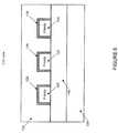
- FIG. 3shows a top view of a portion of a memory cell array having a plurality of memory cells in accordance with an embodiment of the present disclosure.
- FIG. 4shows a first cross-sectional view of a portion of a memory cell array having a plurality of memory cells along line A-A of FIG. 3 in accordance with an embodiment of the present disclosure.
- FIG. 5shows a second cross-sectional view of a portion of a memory cell array having a plurality of memory cells along line B-B of FIG. 3 in accordance with an embodiment of the present disclosure.
- FIG. 6shows a third cross-sectional view of a portion of a memory cell array having a plurality of memory cells along line C-C of FIG. 3 in accordance with an embodiment of the present disclosure.
- FIG. 7shows a top view of a portion of a memory cell array in accordance with an embodiment of the present disclosure.
- FIG. 8shows control signal voltage waveforms for performing a refresh operation on a memory cell in accordance with an embodiment of the present disclosure.
- FIG. 1there is shown a schematic block diagram of a semiconductor memory device 10 comprising a memory cell array 20 , data write and sense circuitry 36 , and memory cell selection and control circuitry 38 in accordance with an embodiment of the present disclosure.
- the memory cell array 20may comprise a plurality of memory cells 12 each connected to the memory cell selection and control circuitry 38 via a word line (WL) 28 , a source line (CN) 30 , and/or a carrier injection line (EP) 34 , and the data write and sense circuitry 36 via a bit line (EN) 32 .
- WLword line
- CNsource line
- EPcarrier injection line
- ENbit line
- the source line (CN) 30 and the bit line (EN) 32are designations used to distinguish between two signal lines and they may be used interchangeably.
- the data write and sense circuitry 36may read data from and may write data to selected memory cells 12 .
- the data write and sense circuitry 36may include a plurality of data sense amplifiers.
- Each data sense amplifiermay receive at least one bit line (EN) 32 and a current or voltage reference signal.
- each data sense amplifiermay be a cross-coupled type sense amplifier to sense a data state stored in a memory cell 12 .
- each data sense amplifiermay employ voltage and/or current sensing circuitry and/or techniques.
- each data sense amplifiermay employ current sensing circuitry and/or techniques.
- a current sense amplifiermay compare current from a selected memory cell 12 to a reference current (e.g., the current of one or more reference cells).
- the selected memory cell 12may be determined whether the selected memory cell 12 contains a logic high (e.g., binary “1” data state) or a logic low (e.g., binary “0” data state). It may be appreciated by one having ordinary skill in the art that various types or forms of data write and sense circuitry 36 (including one or more sense amplifiers, using voltage or current sensing techniques, using or not reference cells, to sense a data state stored in a memory cell 12 ) may be employed to read data stored in memory cells 12 and/or write data to memory cells 12 .
- a logic highe.g., binary “1” data state
- a logic lowe.g., binary “0” data state
- the memory cell selection and control circuitry 38may select and/or enable one or more predetermined memory cells 12 to facilitate reading data therefrom and/or writing data thereto by applying control signals on one or more word lines (WL) 28 , source lines (CN) 30 , and/or carrier injection lines (EP) 34 .
- the memory cell selection and control circuitry 38may generate such control signals from address signals, for example, row address signals.
- the memory cell selection and control circuitry 38may include a word line decoder and/or driver.
- the memory cell selection and control circuitry 38may include one or more different control/selection techniques (and circuitry therefore) to select and/or enable one or more predetermined memory cells 12 . Notably, all such control/selection techniques, and circuitry therefore, whether now known or later developed, are intended to fall within the scope of the present disclosure.
- the semiconductor memory devicemay implement a two step write operation whereby all the memory cells 12 in a row of memory cells 12 may be first written to a predetermined data state.
- the memory cells 12 in a row of memory cells 12may be first written to a logic high (e.g., binary “1” data state) by executing a logic high (e.g., binary “1” data state) write operation.
- a logic highe.g., binary “1” data state
- selected memory cells 12 in the active row of memory cells 12may be selectively written to a logic low (e.g., binary “0” data state) by executing a logic low (e.g., binary “0” data state) write operation.
- the semiconductor memory device 10may also implement a one step write operation whereby selected memory cells 12 in an active row of memory cells 12 may be selectively written to either a logic high (e.g., binary “1” data state) or a logic low (e.g., binary “0” data state) without first implementing a “clear” operation.
- the semiconductor memory device 10may employ any of the exemplary writing, refreshing, holding, and/or reading techniques described herein.
- the memory cells 12may comprise one or more multi-gate devices or multiple gate field effect transistors.
- the memory cells 12may comprise one or more N-type bipolar junction transistors (BJTs), P-type bipolar junction transistors (BJTs) and/or both types of bipolar junction transistors (BJTs).
- Circuitry that is peripheral to the memory array 20for example, sense amplifiers or comparators, row and column address decoders, as well as line drivers (not illustrated herein) may also include P-type and/or N-type bipolar junction transistors (BJTs) or P-type and/or N-type transistors.
- BJTsP-type bipolar junction transistors
- BJTsN-type bipolar junction transistors
- Each of the memory cells 12may comprise a first bipolar junction transistor (BJT) 14 a and a second bipolar junction transistor (BJT) 14 b coupled to each other.
- the first bipolar junction transistor (BJT) 14 a and/or the second bipolar junction transistor (BJT) 14 bmay be an N-type bipolar junction transistor (BJT) or a P-type bipolar junction transistor (BJT). As illustrated in FIG.
- the first bipolar junction transistor (BJT) 14 amay be an N-type bipolar junction transistor (BJT) and the second bipolar junction transistor (BJT) 14 b may be a P-type bipolar junction transistor (BJT).
- the first bipolar junction transistor (BJT) 14 amay be a P-type bipolar junction transistor (BJT) and the second bipolar junction transistor (BJT) 14 b may be an N-type bipolar junction transistor (BJT).
- Each memory cell 12may be coupled to a respective word line (WL) 28 , a respective source line (CN) 30 , a respective bit line (EN) 32 , and a respective carrier injection line (EP) 34 .
- Datamay be written to or read from a selected memory cell 12 by applying suitable control signals to a selected word line (WL) 28 , a selected source line (CN) 30 , a selected bit line (EN) 32 , and/or a selected carrier injection line (EP) 34 .
- each word line (WL) 28 , source line (CN) 30 , and carrier injection line (EP) 34may extend horizontally parallel to each other in a row direction.
- Each bit line (EN) 32may extend vertically in a column direction perpendicular to each word line (WL) 28 , source line (CN) 30 , and/or carrier injection line (EP) 34 .
- one or more respective bit lines (EN) 32may be coupled to one or more data sense amplifiers (not shown) of the data write and sense circuitry 36 to read data states of one or more memory cells 12 in the column direction.
- a data statemay be read from one or more selected memory cells 12 by applying one or more control signals to the one or more selected memory cells 12 via a selected word line (WL) 28 , a selected source line (ON) 30 , and/or a selected carrier injection line (EP) 34 in order to generate a voltage potential and/or a current in the one or more selected memory cells 12 .
- the generated voltage potential and/or currentmay then be output to the data write and sense circuitry 36 via a corresponding bit line (EN) 32 in order to read a data state stored in each selected memory cell 12 .
- a data statemay be read from a selected memory cell 12 via a selected bit line (EN) 32 coupled to the data sense amplifier of the data write and sense circuitry 36 .
- the source line (CN) 30may be separately controlled via a voltage potential/current source (e.g., a voltage potential/current driver) of the memory cell selection and control circuitry 38 .
- the data sense amplifier of the data write and sense circuitry 36 and the voltage potential/current source of the memory cell selection and control circuitry 38may be configured on opposite sides of the memory cell array 20 .
- a data statemay be written to one or more selected memory cells 12 by applying one or more control signals to the one or more selected memory cells 12 via a selected word line (WL) 28 , a selected source line (CN) 30 , a selected bit line (EN) 32 , and/or a selected carrier injection line (EP) 34 .
- WLword line
- CNselected source line
- EPselected carrier injection line
- the one or more control signals applied to the one or more selected memory cells 12 via a selected word line (WL) 28 , a selected source line (CN) 30 , a selected bit line (EN) 32 , and/or a selected carrier injection line (EP) 34may control the first bipolar transistor 14 a and/or the second bipolar transistor 14 b of each selected memory cell 12 in order to write a desired data state to each selected memory cell 12 .
- the memory cell array 20may include a plurality of memory cells 12 arranged in a matrix of rows and columns including a plurality of word lines 28 (WL), a plurality of source lines (CN) 30 , a plurality of bit lines (EN) 32 , and a plurality of carrier injection lines (EP) 34 .
- Each bit line (EN) 32may extend in a first orientation along a first plane of the memory cell array 20 .
- Each source line (CN) 30may extend in a second orientation along a second plane of the memory cell array 20 .
- Each word line (WL) 28may extend in the second orientation along a third plane of the memory cell array 20 .
- Each carrier injection line (EP) 34may extend in the second orientation along a fourth plane in the memory cell array 20 .
- the first plane, the second plane, the third plane, and the fourth planemay be arranged in different planes parallel to each other.
- FIG. 4there is shown a first cross-sectional view of a portion of the memory cell array 20 having a plurality of memory cells 12 in accordance with an embodiment of the present disclosure.
- FIG. 4illustrates a cross-sectional view taken along line (A-A) of the top view shown in FIG. 3 .
- the cross-sectional view of FIG. 4may illustrate a row of memory cells 12 in the memory cell array 20 .
- each row and/or column of the memory cell array 20may include a plurality of memory cells 12 .
- Each memory cell 12may comprise an N+ source region 120 , a P ⁇ body region 122 , an N+ drain region 124 and a P+ injection region 126 .
- the N+ source region 120 , the P ⁇ body region 122 , the N+ region 124 , and/or the P+ injection region 126may be disposed in sequential contiguous relationship, and may extend vertically from a plane defined by a P ⁇ substrate 130 .
- a plurality of memory cells 12 in the row direction of the memory cell array 20may share one or more common regions.
- two contiguous memory cells 12 in the row direction of the memory cell array 20may share the N+ drain region 124 .
- two contiguous memory cells 12 in the row direction of the memory cell array 20may share the P+ injection region 126 .
- the N+ source region 120may be formed of a semiconductor material (e.g., silicon) comprising donor impurities (e.g., nitrogen, arsenic, and/or phosphorus) and coupled to the bit line (EN) 32 .
- the bit line (EN) 32may be formed of a metal material.
- the bit line (EN) 32may be formed of a polycide material (e.g., a combination of a metal material and a silicon material).
- the bit line (EN) 32may be formed of an N+ doped silicon layer.
- the bit line (EN) 32may be connected to a plurality of memory cells 12 (e.g., a column of memory cells 12 ). As shown in FIG. 4 , the bit line (EN) 32 may be formed above the N+ source region 120 .
- the bit line (EN) 32may be connected to a plurality of memory cells 12 (e.g., a column of memory cells 12 ) via a plurality of bit line contacts 132 .
- each bit line contact 132may correspond to a memory cell 12 along a column direction of the memory cell array 20 .
- Each bit line contact 132may be formed of a metal material or polysilicon material in order to couple a predetermined voltage potential from the bit line (EN) 32 to the N+ source region 120 of the memory cell 12 .
- the bit line contact 132may be formed of tungsten, titanium, titanium nitride, polysilicon or a combination thereof.
- the bit line contact 132may have a height extending from the N+ source region 120 of the memory cell 12 to the bit line (EN) 32 .
- the P ⁇ body region 122may be an electrically floating body region of the memory cell 12 configured to accumulate/store charges, and may be spaced apart from and capacitively coupled to the word line (WL) 28 .
- the P ⁇ body region 122may be formed of an undoped semiconductor material (e.g., intrinsic silicon).
- the P ⁇ body region 122may be formed of a semiconductor material (e.g., intrinsic silicon) comprising acceptor impurities.
- the P ⁇ body region 122may be formed of a silicon material doped with boron impurities.
- the P ⁇ body region 122may be formed of an undoped semiconductor material.
- the word line (WL) 28may be formed of a polycide material, a metal material, and/or a combination of a polycide material and a metal material.
- the word line (WL) 28may be oriented in a column direction of the memory cell array 20 and connected to a plurality of memory cells 12 .
- the word line (WL) 28may be arranged above the memory cells 12 (e.g., memory cells 12 located on a column direction of the memory cell array 20 ).
- the word line (WL) 28may be formed of a metal material, a polycide material (e.g., a combination of a metal material and a silicon material), and/or a combination of a metal material and a polycide material.
- the word line (WL) 28may be formed of a P+ doped silicon layer. As illustrated in FIG. 4 , the word line (WL) 28 may be formed of two layers (e.g., a polycide layer and a metal layer). For example, the metal layer may be formed above the polycide layer to couple the polycide layer to a voltage/current source of the memory cell selection and control circuitry 38 .
- the P ⁇ body region 122 and the word line (WL) 28may be capacitively coupled via an insulating or dielectric region 128 .
- the insulating or dielectric region 128may be formed of an insulating material, a dielectric material, or a combination of insulating and dielectric materials.
- the insulating or dielectric region 128may be arranged on one or more sides of the P ⁇ body region 122 to capacitively couple the P ⁇ body region 122 to the word line (WL) 28 in a fin configuration.
- the insulating or dielectric region 128may be arranged above the P ⁇ body region 122 in order to capacitively couple the word line (WL) 28 to the P ⁇ body region 122 .
- the drain region 124 of the memory cell 12may be connected to the source line (CN) 30 .
- the N+ drain region 124may be formed of a semiconductor material (e.g., silicon) comprising donor
- the source line (CN) 30may be formed of a polycide material. In another exemplary embodiment, the source line (ON) 30 may be formed of a metal material. For example, the source line (CN) 30 may be formed of aluminum, copper, tungsten, titanium, titanium nitride, and/or a combination thereof. In another exemplary embodiment, the source line (CN) 30 may be formed of a doped polysilicon material.
- the source line (CN) 30may be connected to a plurality of memory cells 12 (e.g., a column of memory cells 12 ) via a plurality of source line contacts 136 .
- each source line contact 136may correspond to a memory cell 12 along a column direction of the memory cell array 20 .
- Each source line contact 136may be formed of a metal layer or a polysilicon layer in order to couple a predetermined voltage potential from the source line (CN) 30 to the N+ drain region 124 of the memory cell 12 .
- the source line contact 136may be formed of tungsten, titanium, titanium nitride, polysilicon, and/or a combination thereof.
- the source line contact 136may have a height extending from the N+ drain region 124 of the memory cell 12 to the source line (CN) 30 .
- the P+ injection region 126may be directly connected to the carrier injection line (EP) 34 .
- the P+ injection region 126may be formed of a semiconductor material (e.g., silicon) comprising acceptor impurities.
- the P+ injection region 126may be formed of a silicon material doped with boron impurities.
- the P+ injection region 126may be configured as an input region for charges to be injected into the P ⁇ region 122 of the memory cell 12 .
- the charges to be injected into the P ⁇ region 122 of the memory cellmay be supplied by the carrier injection line (EP) 34 and input into the P ⁇ region 122 via the P+ injection region 126 and the N+ region 124 .
- the carrier injection line (EP) 34may be formed of a polycide material, a metal material, or a combination of a polycide material and a metal material. As illustrated in FIG. 4 , the carrier injection line (EP) 34 may be formed of two layers (e.g., a polycide layer arranged below a metal layer). The carrier injection line (EP) 34 may include an ohmic contact to a plurality of sides portions of the P+ injection region 126 in a fin configuration. The carrier injection line (EP) 34 may extend in a column direction of the memory cell array 20 .
- the carrier injection line (EP) 34may extend horizontally in parallel to the word line (WL) 28 and/or the source line (CN) 30 , and may be coupled to a plurality of memory cells 12 (e.g., a row of memory cells 12 ).
- the carrier injection line (EP) 34 , the word line (WL) 28 and/or the source line (CN) 30may be arranged in different planes and configured to be parallel to each other.
- the source line (CN) 30may be arranged in a plane above a plane containing the word line (WL) 28 and a plane containing the carrier injection line (EP) 34 .
- the word lines (WL) 28 and the carrier injection lines (EP)may be separated from the N+ drain region 124 via an insulating/dielectric material 134 .
- the insulating/dielectric material 134may be formed from silicon nitride or silicon dioxide material in order to isolate the N+ drain region 124 from disturbances caused by voltage potentials applied on the word line (WL) 28 and/or the carrier injection line (EP) 34 .
- the insulating/dielectric material 134may circumferentially surround the word line (WL) 28 and/or the carrier injection line (EP) 34 .
- the insulating/dielectric material 134may be arranged between adjacent carrier injection lines (EP) 34 .
- the P ⁇ substrate 130may be made of a semiconductor material (e.g., silicon) comprising acceptor impurities and may form a base of the memory cell array 20 .
- a plurality of P ⁇ substrates 130may form the base of the memory cell array 20 or a single P ⁇ substrate 130 may form the base of the memory cell array 20 .
- the P ⁇ substrate 130may be made in the form of a P-well substrate.
- a plurality of barrier walls 140may be formed on the P ⁇ substrate 130 .
- the plurality of barrier walls 140may be formed of an insulating material.
- the plurality of barrier walls 140may include a continuous planar region configured above the P ⁇ substrate 130 .
- the plurality of barrier walls 140may be formed of an insulating oxide material.
- the plurality of barrier walls 140may be oriented in a column direction and a row direction of the memory cell array 20 .
- a first barrier wall 140 of the plurality of barrier walls 140may be oriented in a column direction.
- a second barrier wall 140 of the plurality of barrier walls 140may be oriented in a row direction.
- the first barrier wall 140 oriented in the column direction and the second barrier wall 140 oriented in the row directionmay be formed on the continuous planar region to form a trench region.
- the trench regionmay have a cross-sectional shape that may accommodate one or more memory cells 12 therein.
- the trench regionmay have a cross-sectional shape of a square, a rectangle, a cylinder, and/or other shapes that may accommodate one or more memory cells 12 .
- FIG. 5there is shown a second cross-sectional view of a portion of the memory cell array 20 having a plurality of memory cells 12 in accordance with an embodiment of the present disclosure.
- FIG. 5illustrates a cross-sectional view taken along line (B-B) of the top view shown in FIG. 3 .
- the cross-sectional view of FIG. 5may illustrate a column of memory cells 12 in the memory cell array 20 .
- each row and/or column of the memory cell array 20may include a plurality of memory cells 12 .
- the P ⁇ body regions 122may be disposed on the continuous planar region of the barrier walls 140 and the P ⁇ substrate 130 .
- the P ⁇ body region 122may be capacitively coupled to the word line (WL) 28 via the insulating or dielectric region 128 .
- the insulating/dielectric material 134may be disposed on top of the word line (WL) 28 .
- the word line (WL) 28may be configured on a plurality of sides of the P ⁇ body region 122 .
- the word line (WL) 28may be arranged to cover the top portion and the side portions of the P ⁇ body region 122 .
- the word line (WL) 28may comprise a metal layer disposed on top of a polycide layer.
- the word line (WL) 28may be capacitively coupled to the P ⁇ body region 122 via the insulating or dielectric region 128 .
- the insulating or dielectric region 128may be disposed to cover a plurality sides of the P ⁇ body region 122 .
- the insulating or dielectric region 128may be disposed to cover the top portion and the side portions of the P ⁇ body region 122 to capacitively couple the word line (WL) 28 and the P ⁇ body region 122 .
- the P ⁇ body region 122 and the word line (WL) 28may be capped by the insulating/dielectric material 134 .
- FIG. 6there is shown a third cross-sectional view of a portion of the memory cell array 20 having a plurality of memory cells 12 in accordance with an embodiment of the present disclosure.
- FIG. 6illustrates a cross-sectional view taken along line (C-C) of the top view shown in FIG. 3 .
- the cross-sectional view of FIG. 6may illustrate a column of memory cells 12 in the memory cell array 20 .
- each row and/or column of the memory cell array 20may include a plurality of memory cells 12 .
- the P ⁇ body regions 122may be disposed on the continuous planar region of the barrier walls 140 and the P ⁇ substrate 130 .
- the P ⁇ body region 1224may be capacitively coupled to the word line (WL) 28 via the insulating or dielectric region 128 .
- the insulating/dielectric material 134may be disposed on top of the word line (WL) 28 .
- the memory cell array 20may include a plurality of memory cells 12 arranged in a matrix of rows and columns including a plurality of source lines (CN) 30 and a plurality of bit lines (EN) 32 .
- Each bit line (EN) 32may extend in a first orientation along a first plane of the memory cell array 20 .
- Each source line (CN) 30may extend in a second orientation along a second plane of the memory cell array 20 .
- Each source line (CN) 30may be coupled to a plurality of memory cells 12 (e.g., a column of memory cells 12 ) via a plurality of corresponding source line contacts 136 .
- each source line contact 136may correspond to a memory cell 12 along a column direction of the memory cell array 20 .
- each bit line (EN) 32may be connected to a plurality of memory cells (e.g., a row of memory cells 12 ) via a plurality of corresponding bit line contacts 132 .
- each bit line contact 132may correspond to a memory cell 12 along a row direction of the memory cell array 20 .
- the refresh operationmay include control signals configured to perform one or more sub-operations.
- the refresh operationmay include a read operation, a write logic high (e.g., binary “1” data state) operation, and/or a write logic low (e.g., binary “0” data state) operation.
- control signalsPrior to performing the refresh operation, the control signals may be configured to perform a hold operation in order to maintain a data state (e.g., a logic high (binary “1” data state) or a logic low (binary “0” data state)) stored in the memory cell 12 .
- the control signalsmay be configured to perform a hold operation in order to maximize a retention time of a data state (e.g., a logic low (binary “0” data state) and/or a logic high (binary “1” data state)) stored in the memory cell 12 .
- the control signals for the hold operationmay be configured to eliminate or reduce activities or fields (e.g., electrical fields between junctions which may lead to leakage of charges) within the memory cell 12 .
- a negative voltage potentialmay be applied to the word line (WL) (which is capacitively coupled to the P ⁇ region 122 of the memory cell 12 ), while voltage potentials applied to other regions (e.g., the N+ region 120 , the N+ region 124 , and/or the P+ region 126 ) may be maintained at approximately 0V.
- the negative voltage potential applied to the word line (WL) 28may be ⁇ 1.5V.
- the junction between the N+ region 124 and the P ⁇ region 122 and the junction between the N+ region 120 and the P ⁇ region 122may be reverse biased in order to retain a data state (e.g., a logic high (binary “1” data state) or a logic low (binary “0” data state)) stored in the memory cell 12 .
- a data statee.g., a logic high (binary “1” data state) or a logic low (binary “0” data state) stored in the memory cell 12 .
- a refresh operationmay include a read operation during which the control signals may be configured to read a data state (e.g., a logic low (binary “0” data state) and/or a logic high (binary “1” data state)) stored in one or more selected memory cells 12 of one or more selected rows of the memory cell array 20 .
- the control signalsmay be configured to a predetermined voltage potential to implement a read operation via the bit line (EN) 32 .
- a voltage potential applied to the word line (WL) 28(which is capacitively coupled to the P ⁇ region 122 ) and/or a voltage potential applied to the N+ region 124 via the source line (CN) 30 may be raised to a predetermined voltage potential in order to read a data state stored in the memory cell 12 .
- the voltage potential applied to the word line (WL) 28may be raised to 0V from ⁇ 1.5V, while the voltage potential applied to the N+ region 124 of the memory cell 12 may be raised to 1.2V from 0V.
- the voltage potential applied to the word line (WL) 28may be raised to 0V and the voltage potential applied to the source line (CN) may be raised to 1.2V.
- the junction between the P ⁇ region 122 and the N+ region 120may become forward biased.
- the junction between the P ⁇ region 122 and the N+ region 124may be reverse biased or become weakly forward biased (e.g., above the reverse bias voltage and below forward bias threshold voltage, and/or the voltage potential at a p-diffusion region between the P ⁇ region 122 and the N+ region 124 is higher than the voltage potential at the n-diffusion region between the P ⁇ region 122 and the N+ region 124 ).
- a voltage potential or currentmay be generated when forward biasing the junction between the P ⁇ region 122 and the N+ region 120 .
- the voltage potential or current generatedmay be detected by a data sense amplifier in the data write and sense circuitry 36 via the bit line (EN) 32 coupled to the N+ region 120 .
- An amount of voltage potential or current generatedmay be representative of a data state (e.g., a logic low (binary “0” data state) and/or a logic high (binary “1” data state)) stored in the memory cell 12 .
- the junction between the P ⁇ region 122 and the N+ region 120may remain reverse biased or become weakly forward biased (e.g., above the reverse bias voltage and below forward bias threshold voltage, and/or the voltage potential at a p-diffusion region between the P ⁇ region 122 and the N+ region 120 is higher than the voltage potential at the n-diffusion region between the P ⁇ region 122 and the N+ region 120 ).
- a small amount of voltage potential and current or no voltage potential and currentmay be generated when the junction between the P ⁇ region 122 and the N+ region 120 is reverse biased or weakly forward biased.
- a data sense amplifier in the data write and sense circuitry 36may detect the small amount of voltage potential and current or no voltage potential and current via the bit line (EN) 32 coupled to the N+ region 120 .
- a logic highe.g., binary “1” data state
- the junction between the P ⁇ region 122 and the N+ region 120may become forward biased.
- a larger amount of voltage potential or currente.g., compared to a reference voltage potential or current
- a data sense amplifier in the data write and sense circuitry 36may detect the larger amount of voltage potential or current via the bit line (EN) 32 coupled to the N+ region 120 .
- a refresh operationmay include a write logic high (e.g., binary “1” data state) operation where the control signals may be configured to write a logic high (e.g., binary “1” data state) to one or more selected memory cells 12 of one or more selected rows of the memory cell array 20 .
- the write logic high (e.g., binary “1” data state) operationmay be performed via a corresponding bit line (EN(“ 1 ”)) 32 .
- the write logic high (e.g., binary “1” data state) operationmay be performed on one or more selected rows of the memory cell array 20 , or the entire memory cell array 20 , and a subsequent write logic low (e.g., binary “0” data state) operation may be performed on one or more selected memory cells 12 .
- a voltage potential applied to the N+ region 120 via the corresponding bit line (EN(“ 1 ”)) 32 of the memory cells 12may be maintained at 0V.
- the voltage potential applied to the word line (WL) 28(which is capacitively coupled to the P ⁇ region 122 ) may be lowered to ⁇ 1.5V.
- a voltage potential applied to the N+ region 124 of the memory cells 12may be lowered to 0V.
- a voltage potential applied to the carrier injection line (EP) 34may be raised to 1.0V from 0V.
- the junction between the N+ region 120 and the P ⁇ region 122may be reverse biased and the junction between the P+ region 126 and the N+ region 124 may become forward biased.
- a logic highe.g., binary “1” data state
- the voltage potential at the P ⁇ region 122may increase to approximately 0V to 0.7V above the voltage potential at N+ region 124 .
- the first bipolar junction transistor (BJT) 14 amay start to switch to an “ON” state and the current generated by the first bipolar junction transistor (BJT) 14 a may increase to approximately the same as the current generated by the second bipolar junction transistor (BJT) 14 b .
- the current generated by the first bipolar junction transistor (BJT) 14 a and the current generated by the second bipolar junction transistor (BJT) 14 bmay cause the P ⁇ region 122 to reach a steady state potential after the write logic high (e.g., binary “1” data state) operation has been completed.
- the write logic highe.g., binary “1” data state
- a refresh operationmay include a write logic low (e.g., binary “0” data state) operation during which the control signals may be configured to perform one or more write operations to one or more selected memory cells 12 .
- the write logic low (e.g., binary “0” data state) operationmay be performed via a corresponding bit line (EN(“ 0 ”)) 32 .
- the write logic low (e.g., binary “0” data state) operationmay be performed to one or more selected memory cells after a write logic high (e.g., binary “1” data state) operation in order to deplete majority charge carriers that may have accumulated in the P ⁇ regions 122 of the one or more selected memory cells 12 .
- a voltage potential applied to the N+ region 120 via the bit line (EN(“ 0 ”)) 32may be maintained at 0V in order to perform the write logic low (e.g., binary “0” data state) operation.
- a voltage potential applied to the N+ region 124 via the source line (CN) 30may be raised to 1.2V from 0V.
- a voltage potential applied to the word line (WL) 28may be raised to approximately 0V from ⁇ 1.5V.
- the junction between the N+ region 120 and the P ⁇ region 122may become forward biased and the first bipolar junction transistor (BJT) 14 a (e.g., regions 120 - 124 ) may be switched to an “ON” state.
- the majority charge carriers that may have accumulated in the P ⁇ region 122 during the write logic high (e.g., binary “1” data state) operationmay be removed via the forward biased junction between the N+ region 120 and the P ⁇ region 122 .
- the memory cell 12may represent a logic low (e.g., binary “0” data state).
- masking operationmay be performed on the one or more unselected memory cells 12 .
- the voltage potential applied to the N+ region 120 via the bit line (EN(“ 1 ”)) of the one or more unselected memory cells 12may be raised to 1.2V or higher (e.g., 1.5V) in order to prevent the depletion of majority charge carriers accumulated in the P ⁇ region 122 .
- the junction between the N+ region 120 and the P ⁇ region 122may not be forward biased and the junction between the P ⁇ region 122 and the N+ region 124 may not be forward biased in order to prevent the depletion of majority charge carriers accumulated in the P ⁇ region 122 .
- the logic highe.g., binary “1” data state
- the control signalsmay be configured to perform a hold operation.
- providing a direct injection semiconductor memory device in accordance with the present disclosure as described abovetypically involves the processing of input data and the generation of output data to some extent.
- This input data processing and output data generationmay be implemented in hardware or software.
- specific electronic componentsmay be employed in a direct injection semiconductor memory device or similar or related circuitry for implementing the functions associated with providing a direct injection semiconductor memory device in accordance with the present disclosure as described above.
- one or more processors operating in accordance with instructionsmay implement the functions associated with providing a direct injection semiconductor memory device in accordance with the present disclosure as described above.
- Such instructionsmay be stored on one or more processor readable media (e.g., a magnetic disk or other storage medium), or transmitted to one or more processors via one or more signals embodied in one or more carrier waves.
- processor readable mediae.g., a magnetic disk or other storage medium
Landscapes
- Engineering & Computer Science (AREA)
- Microelectronics & Electronic Packaging (AREA)
- Computer Hardware Design (AREA)
- Semiconductor Memories (AREA)
Abstract
Description
- This patent application claims priority to U.S. Provisional Patent Application No. 61/180,810, filed May 22, 2009, which is hereby incorporated by reference herein in its entirety.
- The present disclosure relates generally to semiconductor memory devices and, more particularly, to techniques for providing a direct injection semiconductor memory device.
- The semiconductor industry has experienced technological advances that have permitted increases in density and/or complexity of semiconductor memory devices. Also, the technological advances have allowed decreases in power consumption and package sizes of various types of semiconductor memory devices. There is a continuing trend to employ and/or fabricate advanced semiconductor memory devices using techniques, materials, and devices that improve performance, reduce leakage current, and enhance overall scaling. Silicon-on-insulator (SOI) and bulk substrates are examples of materials that may be used to fabricate such semiconductor memory devices. Such semiconductor memory devices may include, for example, partially depleted (PD) devices, fully depleted (FD) devices, multiple gate devices (for example, double, triple, or surrounding gate), and bipolar junction transistor (BJT) devices.
- A semiconductor memory device may include a memory cell having a memory transistor with an electrically floating body region wherein electrical charges may be stored. When excess majority electrical charge carriers are stored in the electrically floating body region, the memory cell may store a logic high (e.g., binary “1” data state). When the electrical floating body region is depleted of majority electrical charge carriers, the memory cell may store a logic low (e.g., binary “0” data state). Also, a semiconductor memory device may be fabricated on silicon-on-insulator (SOI) substrates or bulk substrates (e.g., enabling body isolation). For example, a semiconductor memory device may be fabricated as a three-dimensional (3-D) device (e.g., multiple gate devices, bipolar junction transistors (BJTs), recessed gates and pillars) on a silicon-on-insulator (SOI) or bulk substrates.
- In one conventional technique, the memory cell of the semiconductor memory device may be read by applying bias signals to a source/drain regions and/or a gate of the memory transistor. As such, a conventional reading technique may involve sensing an amount of current provided/generated by/in the electrically floating body region of the memory cell in response to the application of the source/drain region and/or gate bias signals to determine a data state stored in the memory cell. For example, the memory cell may have two or more different current states corresponding to two or more different logical states (e.g., two different current conditions/states corresponding to two different logic states: a binary “0” data state and a binary “1” data state).
- In another conventional technique, the memory cell of the semiconductor memory device may be written to by applying bias signals to the source/drain region(s) and/or the gate of the memory transistor. As such, a conventional writing technique may result in an increase/decrease of majority charge carriers in the electrically floating body region of the memory cell which, in turn, may determine the data state of the memory cell. An increase of majority charge carriers in the electrically floating body region may result from impact ionization, band-to-band tunneling (gate-induced drain leakage “GIDL”), or direct injection. A decrease of majority charge carriers in the electrically floating body region may result from charge carriers being removed via drain region charge carrier removal, source region charge carrier removal, or drain and source region charge carrier removal, for example, using back gate pulsing.
- Often, conventional reading and/or writing operations may lead to relatively large power consumption and large voltage potential swings which may cause disturbance to unselected memory cells in the semiconductor memory device. Also, pulsing between positive and negative gate biases during read and write operations may reduce a net quantity of majority charge carriers in the electrically floating body region of the memory cell in the semiconductor memory device, which, in turn, may result in an inaccurate determination of the state of the memory cell. Furthermore, in the event that a bias is applied to the gate of the memory transistor that is below a threshold voltage potential of the memory transistor, a channel of minority charge carriers beneath the gate may be eliminated. However, some of the minority charge carriers may remain “trapped” in interface defects. Some of the trapped minority charge carriers may recombine with majority charge carriers, which may be attracted to the gate as a result of the applied bias. As a result, the net quantity of majority charge carriers in the electrically floating body region may be reduced. This phenomenon, which is typically characterized as charge pumping, is problematic because the net quantity of majority charge carriers may be reduced in the electrically floating body region of the memory cell, which, in turn, may result in an inaccurate determination of the state of the memory cell.
- In view of the foregoing, it may be understood that there may be significant problems and shortcomings associated with conventional techniques for operating semiconductor memory devices.
- Techniques for providing a direct injection semiconductor memory device are disclosed. In one particular exemplary embodiment, the techniques may be realized as a direct injection semiconductor memory device comprising a first region connected to a bit line extending in a first orientation and a second region connected to a source line extending in a second orientation. The direct injection semiconductor memory device may also comprise a body region spaced apart from and capacitively coupled to a word line extending in the second orientation, wherein the body region is electrically floating and disposed between the first region and the second region. The direct injection semiconductor memory device may further comprise a third region connected to a carrier injection line extending in the second orientation, wherein the first region, the second region, the body region, and the third region are disposed in sequential contiguous relationship.
- In accordance with other aspects of the particular exemplary embodiment, the first region and the second region may be N− doped regions.
- In accordance with further aspects of this particular exemplary embodiment, the body region and the third region may be a P− doped region.
- In accordance with additional aspects of this particular exemplary embodiment, the first region, the body region, and the second regions may form a first bipolar junction transistor (BJT).
- In accordance with yet another aspect of this particular exemplary embodiment, the body region, the second region, and the third region may form a second bipolar junction transistor (BJT).
- In accordance with other aspects of the particular exemplary embodiment, the bit line may be connected to the first region via a bit line contact.
- In accordance with further aspects of this particular exemplary embodiment, the source line may be connected to the second region via a source line contact.
- In accordance with additional aspects of this particular exemplary embodiment, the word line may be circumferentially surrounded by an insulating/dielectric material.
- In accordance with yet another aspect of this particular exemplary embodiment, the carrier injection line may be circumferentially surrounded by an insulating/dielectric material.
- In accordance with other aspects of the particular exemplary embodiment, the carrier injection line may include an ohmic contact on a plurality of side portions of the third region in a fin configuration.
- In accordance with further aspects of this particular exemplary embodiment, the word line may be disposed to cover a plurality of side portions of the body region in a fin configuration.
- In accordance with additional aspects of this particular exemplary embodiment, the device may further comprise a plurality of barrier walls configured on a continuous planar region.
- In accordance with yet another aspect of this particular exemplary embodiment, the device may further comprise a substrate disposed below the plurality of barrier walls.
- In another exemplary embodiment, the technique may be realized as a method for biasing a direct injection semiconductor memory device. The method may comprise applying a first voltage potential to a first region via a bit line extending in a first orientation and applying a second voltage potential to a second region via a source line extending in a second orientation. The method may also comprise applying a third voltage potential to a body region via a word line extending in the second orientation, wherein the body region is electrically floating and capacitively coupled to the word line. The method may further comprise applying a fourth voltage potential to a third region via a carrier injection line extending in the second orientation, wherein the first region, the second region, the body region, and the third region are disposed in sequential contiguous relationship.
- In accordance with other aspects of the particular exemplary embodiment, the method may further comprise increasing the third voltage potential applied to the word line from the third voltage potential applied to the word line during a hold operation to perform a read operation.
- In accordance with further aspects of this particular exemplary embodiment, the method may further comprise increasing the second voltage potential applied to the source line from the second voltage potential applied to the source line during a hold operation to perform a read operation.
- In accordance with additional aspects of this particular exemplary embodiment, the method may further comprise maintaining the first voltage potential applied during a hold operation and maintaining the fourth voltage potential applied to the carrier injection line during the hold operation to perform a read operation.
- In accordance with yet another aspect of this particular exemplary embodiment, the method may further comprise maintaining the third voltage potential applied to the word line from the third voltage potential applied to the word line during a hold operation to perform a write logic high operation.
- In accordance with other aspects of the particular exemplary embodiment, the method may further comprise maintaining the second voltage potential applied to the second region via the source line from the second voltage potential applied to the second region during a hold operation to perform a write logic high operation.
- In accordance with further aspects of this particular exemplary embodiment, the method may further comprise increasing the fourth voltage potential applied to the third region via the carrier injection line from the fourth voltage applied to the third region during a hold operation to perform a write logic high operation.
- In accordance with additional aspects of this particular exemplary embodiment, the method may further comprise increasing the third voltage potential applied to the word line from the third voltage potential applied to the word line during a hold operation to perform a write logic low operation.
- In accordance with yet another aspect of this particular exemplary embodiment, the method may further comprise increasing the second voltage potential applied to the source line from the second voltage potential applied to the source line during a hold operation to perform a write logic low operation.
- In accordance with other aspects of the particular exemplary embodiment, the method may further comprise maintaining the first voltage potential applied to the bit line from the first voltage potential applied to the bit line during a hold operation to perform a write logic low operation.
- In accordance with further aspects of this particular exemplary embodiment, the method may further comprise increasing the first voltage potential applied to the bit line during a write logic low operation from the first voltage potential applied to the bit line during a hold operation to maintain a logic high stored in the memory cell.
- The present disclosure will now be described in more detail with reference to exemplary embodiments thereof as shown in the accompanying drawings. While the present disclosure is described below with reference to exemplary embodiments, it should be understood that the present disclosure is not limited thereto. Those of ordinary skill in the art having access to the teachings herein will recognize additional implementations, modifications, and embodiments, as well as other fields of use, which are within the scope of the present disclosure as described herein, and with respect to which the present disclosure may be of significant utility.
- In order to facilitate a fuller understanding of the present disclosure, reference is now made to the accompanying drawings, in which like elements are referenced with like numerals. These drawings should not be construed as limiting the present disclosure, but are intended to be exemplary only.
FIG. 1 shows a schematic block diagram of a semiconductor memory device including a memory cell array, data write and sense circuitry, and memory cell selection and control circuitry in accordance with an embodiment of the present disclosure.FIG. 2 shows a schematic diagram of at least a portion of a memory cell array having a plurality of memory cells in accordance with an embodiment of the present disclosure.FIG. 3 shows a top view of a portion of a memory cell array having a plurality of memory cells in accordance with an embodiment of the present disclosure.FIG. 4 shows a first cross-sectional view of a portion of a memory cell array having a plurality of memory cells along line A-A ofFIG. 3 in accordance with an embodiment of the present disclosure.FIG. 5 shows a second cross-sectional view of a portion of a memory cell array having a plurality of memory cells along line B-B ofFIG. 3 in accordance with an embodiment of the present disclosure.FIG. 6 shows a third cross-sectional view of a portion of a memory cell array having a plurality of memory cells along line C-C ofFIG. 3 in accordance with an embodiment of the present disclosure.FIG. 7 shows a top view of a portion of a memory cell array in accordance with an embodiment of the present disclosure.FIG. 8 shows control signal voltage waveforms for performing a refresh operation on a memory cell in accordance with an embodiment of the present disclosure.- Referring to
FIG. 1 , there is shown a schematic block diagram of asemiconductor memory device 10 comprising amemory cell array 20, data write andsense circuitry 36, and memory cell selection andcontrol circuitry 38 in accordance with an embodiment of the present disclosure. Thememory cell array 20 may comprise a plurality ofmemory cells 12 each connected to the memory cell selection andcontrol circuitry 38 via a word line (WL)28, a source line (CN)30, and/or a carrier injection line (EP)34, and the data write andsense circuitry 36 via a bit line (EN)32. It may be appreciated that the source line (CN)30 and the bit line (EN)32 are designations used to distinguish between two signal lines and they may be used interchangeably. - The data write and
sense circuitry 36 may read data from and may write data to selectedmemory cells 12. In an exemplary embodiment, the data write andsense circuitry 36 may include a plurality of data sense amplifiers. Each data sense amplifier may receive at least one bit line (EN)32 and a current or voltage reference signal. For example, each data sense amplifier may be a cross-coupled type sense amplifier to sense a data state stored in amemory cell 12. Also, each data sense amplifier may employ voltage and/or current sensing circuitry and/or techniques. In an exemplary embodiment, each data sense amplifier may employ current sensing circuitry and/or techniques. For example, a current sense amplifier may compare current from a selectedmemory cell 12 to a reference current (e.g., the current of one or more reference cells). From that comparison, it may be determined whether the selectedmemory cell 12 contains a logic high (e.g., binary “1” data state) or a logic low (e.g., binary “0” data state). It may be appreciated by one having ordinary skill in the art that various types or forms of data write and sense circuitry36 (including one or more sense amplifiers, using voltage or current sensing techniques, using or not reference cells, to sense a data state stored in a memory cell12) may be employed to read data stored inmemory cells 12 and/or write data tomemory cells 12. - The memory cell selection and
control circuitry 38 may select and/or enable one or morepredetermined memory cells 12 to facilitate reading data therefrom and/or writing data thereto by applying control signals on one or more word lines (WL)28, source lines (CN)30, and/or carrier injection lines (EP)34. The memory cell selection andcontrol circuitry 38 may generate such control signals from address signals, for example, row address signals. Moreover, the memory cell selection andcontrol circuitry 38 may include a word line decoder and/or driver. For example, the memory cell selection andcontrol circuitry 38 may include one or more different control/selection techniques (and circuitry therefore) to select and/or enable one or morepredetermined memory cells 12. Notably, all such control/selection techniques, and circuitry therefore, whether now known or later developed, are intended to fall within the scope of the present disclosure. - In an exemplary embodiment, the semiconductor memory device may implement a two step write operation whereby all the
memory cells 12 in a row ofmemory cells 12 may be first written to a predetermined data state. For example, thememory cells 12 in a row ofmemory cells 12 may be first written to a logic high (e.g., binary “1” data state) by executing a logic high (e.g., binary “1” data state) write operation. Thereafter, selectedmemory cells 12 in the active row ofmemory cells 12 may be selectively written to a logic low (e.g., binary “0” data state) by executing a logic low (e.g., binary “0” data state) write operation. Thesemiconductor memory device 10 may also implement a one step write operation whereby selectedmemory cells 12 in an active row ofmemory cells 12 may be selectively written to either a logic high (e.g., binary “1” data state) or a logic low (e.g., binary “0” data state) without first implementing a “clear” operation. Thesemiconductor memory device 10 may employ any of the exemplary writing, refreshing, holding, and/or reading techniques described herein. - The
memory cells 12 may comprise one or more multi-gate devices or multiple gate field effect transistors. In an exemplary embodiment, thememory cells 12 may comprise one or more N-type bipolar junction transistors (BJTs), P-type bipolar junction transistors (BJTs) and/or both types of bipolar junction transistors (BJTs). Circuitry that is peripheral to the memory array20 (for example, sense amplifiers or comparators, row and column address decoders, as well as line drivers (not illustrated herein)) may also include P-type and/or N-type bipolar junction transistors (BJTs) or P-type and/or N-type transistors. Regardless of whether P-type bipolar junction transistors (BJTs) or N-type bipolar junction transistors (BJTs) are employed inmemory cells 12 in thememory array 20, suitable voltage potentials (for example, positive or negative voltage potentials) for reading from and/or writing to thememory cells 12 may be applied. - Referring to
FIG. 2 , there is shown a schematic diagram of at least a portion of thememory cell array 20 having the plurality ofmemory cells 12 in accordance with an embodiment of the present disclosure. Each of thememory cells 12 may comprise a first bipolar junction transistor (BJT)14aand a second bipolar junction transistor (BJT)14bcoupled to each other. For example, the first bipolar junction transistor (BJT)14aand/or the second bipolar junction transistor (BJT)14bmay be an N-type bipolar junction transistor (BJT) or a P-type bipolar junction transistor (BJT). As illustrated inFIG. 2 , the first bipolar junction transistor (BJT)14amay be an N-type bipolar junction transistor (BJT) and the second bipolar junction transistor (BJT)14bmay be a P-type bipolar junction transistor (BJT). In another exemplary embodiment, the first bipolar junction transistor (BJT)14amay be a P-type bipolar junction transistor (BJT) and the second bipolar junction transistor (BJT)14bmay be an N-type bipolar junction transistor (BJT). - Each
memory cell 12 may be coupled to a respective word line (WL)28, a respective source line (CN)30, a respective bit line (EN)32, and a respective carrier injection line (EP)34. Data may be written to or read from a selectedmemory cell 12 by applying suitable control signals to a selected word line (WL)28, a selected source line (CN)30, a selected bit line (EN)32, and/or a selected carrier injection line (EP)34. In an exemplary embodiment, each word line (WL)28, source line (CN)30, and carrier injection line (EP)34 may extend horizontally parallel to each other in a row direction. Each bit line (EN)32 may extend vertically in a column direction perpendicular to each word line (WL)28, source line (CN)30, and/or carrier injection line (EP)34. - In an exemplary embodiment, one or more respective bit lines (EN)32 may be coupled to one or more data sense amplifiers (not shown) of the data write and
sense circuitry 36 to read data states of one ormore memory cells 12 in the column direction. A data state may be read from one or moreselected memory cells 12 by applying one or more control signals to the one or moreselected memory cells 12 via a selected word line (WL)28, a selected source line (ON)30, and/or a selected carrier injection line (EP)34 in order to generate a voltage potential and/or a current in the one or moreselected memory cells 12. The generated voltage potential and/or current may then be output to the data write andsense circuitry 36 via a corresponding bit line (EN)32 in order to read a data state stored in each selectedmemory cell 12. - In an exemplary embodiment, a data state may be read from a selected
memory cell 12 via a selected bit line (EN)32 coupled to the data sense amplifier of the data write andsense circuitry 36. The source line (CN)30 may be separately controlled via a voltage potential/current source (e.g., a voltage potential/current driver) of the memory cell selection andcontrol circuitry 38. In an exemplary embodiment, the data sense amplifier of the data write andsense circuitry 36 and the voltage potential/current source of the memory cell selection andcontrol circuitry 38 may be configured on opposite sides of thememory cell array 20. - In an exemplary embodiment, a data state may be written to one or more
selected memory cells 12 by applying one or more control signals to the one or moreselected memory cells 12 via a selected word line (WL)28, a selected source line (CN)30, a selected bit line (EN)32, and/or a selected carrier injection line (EP)34. The one or more control signals applied to the one or moreselected memory cells 12 via a selected word line (WL)28, a selected source line (CN)30, a selected bit line (EN)32, and/or a selected carrier injection line (EP)34 may control the firstbipolar transistor 14aand/or the secondbipolar transistor 14bof each selectedmemory cell 12 in order to write a desired data state to each selectedmemory cell 12. - Referring to
FIG. 3 , there is shown a top view of a portion of thememory cell array 20 having a plurality ofmemory cells 12 in accordance with an embodiment of the present disclosure. As illustrated in the top view, thememory cell array 20 may include a plurality ofmemory cells 12 arranged in a matrix of rows and columns including a plurality of word lines28 (WL), a plurality of source lines (CN)30, a plurality of bit lines (EN)32, and a plurality of carrier injection lines (EP)34. Each bit line (EN)32 may extend in a first orientation along a first plane of thememory cell array 20. Each source line (CN)30 may extend in a second orientation along a second plane of thememory cell array 20. Each word line (WL)28 may extend in the second orientation along a third plane of thememory cell array 20. Each carrier injection line (EP)34 may extend in the second orientation along a fourth plane in thememory cell array 20. The first plane, the second plane, the third plane, and the fourth plane may be arranged in different planes parallel to each other. - Referring to
FIG. 4 , there is shown a first cross-sectional view of a portion of thememory cell array 20 having a plurality ofmemory cells 12 in accordance with an embodiment of the present disclosure. For example,FIG. 4 illustrates a cross-sectional view taken along line (A-A) of the top view shown inFIG. 3 . The cross-sectional view ofFIG. 4 may illustrate a row ofmemory cells 12 in thememory cell array 20. In an exemplary embodiment, each row and/or column of thememory cell array 20 may include a plurality ofmemory cells 12. Eachmemory cell 12 may comprise anN+ source region 120, a P−body region 122, anN+ drain region 124 and aP+ injection region 126. TheN+ source region 120, the P−body region 122, theN+ region 124, and/or theP+ injection region 126 may be disposed in sequential contiguous relationship, and may extend vertically from a plane defined by a P−substrate 130. - In an exemplary embodiment, a plurality of
memory cells 12 in the row direction of thememory cell array 20 may share one or more common regions. For example, twocontiguous memory cells 12 in the row direction of thememory cell array 20 may share theN+ drain region 124. Alternatively, twocontiguous memory cells 12 in the row direction of thememory cell array 20 may share theP+ injection region 126. - In an exemplary embodiment, the
N+ source region 120 may be formed of a semiconductor material (e.g., silicon) comprising donor impurities (e.g., nitrogen, arsenic, and/or phosphorus) and coupled to the bit line (EN)32. In an exemplary embodiment, the bit line (EN)32 may be formed of a metal material. In another exemplary embodiment, the bit line (EN)32 may be formed of a polycide material (e.g., a combination of a metal material and a silicon material). In another exemplary embodiment, the bit line (EN)32 may be formed of an N+ doped silicon layer. The bit line (EN)32 may be connected to a plurality of memory cells12 (e.g., a column of memory cells12). As shown inFIG. 4 , the bit line (EN)32 may be formed above theN+ source region 120. - The bit line (EN)32 may be connected to a plurality of memory cells12 (e.g., a column of memory cells12) via a plurality of
bit line contacts 132. For example, eachbit line contact 132 may correspond to amemory cell 12 along a column direction of thememory cell array 20. Eachbit line contact 132 may be formed of a metal material or polysilicon material in order to couple a predetermined voltage potential from the bit line (EN)32 to theN+ source region 120 of thememory cell 12. For example, thebit line contact 132 may be formed of tungsten, titanium, titanium nitride, polysilicon or a combination thereof. Thebit line contact 132 may have a height extending from theN+ source region 120 of thememory cell 12 to the bit line (EN)32. - In an exemplary embodiment, the P−
body region 122 may be an electrically floating body region of thememory cell 12 configured to accumulate/store charges, and may be spaced apart from and capacitively coupled to the word line (WL)28. In an exemplary embodiment, the P−body region 122 may be formed of an undoped semiconductor material (e.g., intrinsic silicon). In another exemplary embodiment, the P−body region 122 may be formed of a semiconductor material (e.g., intrinsic silicon) comprising acceptor impurities. For example, the P−body region 122 may be formed of a silicon material doped with boron impurities. In other exemplary embodiments, the P−body region 122 may be formed of an undoped semiconductor material. - The word line (WL)28 may be formed of a polycide material, a metal material, and/or a combination of a polycide material and a metal material. The word line (WL)28 may be oriented in a column direction of the
memory cell array 20 and connected to a plurality ofmemory cells 12. The word line (WL)28 may be arranged above the memory cells12 (e.g.,memory cells 12 located on a column direction of the memory cell array20). In an exemplary embodiment, the word line (WL)28 may be formed of a metal material, a polycide material (e.g., a combination of a metal material and a silicon material), and/or a combination of a metal material and a polycide material. In another exemplary embodiment, the word line (WL)28 may be formed of a P+ doped silicon layer. As illustrated inFIG. 4 , the word line (WL)28 may be formed of two layers (e.g., a polycide layer and a metal layer). For example, the metal layer may be formed above the polycide layer to couple the polycide layer to a voltage/current source of the memory cell selection andcontrol circuitry 38. - The P−
body region 122 and the word line (WL)28 may be capacitively coupled via an insulating ordielectric region 128. The insulating ordielectric region 128 may be formed of an insulating material, a dielectric material, or a combination of insulating and dielectric materials. In an exemplary embodiment, the insulating ordielectric region 128 may be arranged on one or more sides of the P−body region 122 to capacitively couple the P−body region 122 to the word line (WL)28 in a fin configuration. In another exemplary embodiment, the insulating ordielectric region 128 may be arranged above the P−body region 122 in order to capacitively couple the word line (WL)28 to the P−body region 122. - In an exemplary embodiment, the
drain region 124 of thememory cell 12 may be connected to the source line (CN)30. In an exemplary embodiment, theN+ drain region 124 may be formed of a semiconductor material (e.g., silicon) comprising donor - In an exemplary embodiment, the source line (CN)30 may be formed of a polycide material. In another exemplary embodiment, the source line (ON)30 may be formed of a metal material. For example, the source line (CN)30 may be formed of aluminum, copper, tungsten, titanium, titanium nitride, and/or a combination thereof. In another exemplary embodiment, the source line (CN)30 may be formed of a doped polysilicon material.
- The source line (CN)30 may be connected to a plurality of memory cells12 (e.g., a column of memory cells12) via a plurality of
source line contacts 136. For example, eachsource line contact 136 may correspond to amemory cell 12 along a column direction of thememory cell array 20. Eachsource line contact 136 may be formed of a metal layer or a polysilicon layer in order to couple a predetermined voltage potential from the source line (CN)30 to theN+ drain region 124 of thememory cell 12. For example, thesource line contact 136 may be formed of tungsten, titanium, titanium nitride, polysilicon, and/or a combination thereof. Thesource line contact 136 may have a height extending from theN+ drain region 124 of thememory cell 12 to the source line (CN)30. - The
P+ injection region 126 may be directly connected to the carrier injection line (EP)34. TheP+ injection region 126 may be formed of a semiconductor material (e.g., silicon) comprising acceptor impurities. For example, theP+ injection region 126 may be formed of a silicon material doped with boron impurities. In an exemplary embodiment, theP+ injection region 126 may be configured as an input region for charges to be injected into the P−region 122 of thememory cell 12. The charges to be injected into the P−region 122 of the memory cell may be supplied by the carrier injection line (EP)34 and input into the P−region 122 via theP+ injection region 126 and theN+ region 124. - The carrier injection line (EP)34 may be formed of a polycide material, a metal material, or a combination of a polycide material and a metal material. As illustrated in
FIG. 4 , the carrier injection line (EP)34 may be formed of two layers (e.g., a polycide layer arranged below a metal layer). The carrier injection line (EP)34 may include an ohmic contact to a plurality of sides portions of theP+ injection region 126 in a fin configuration. The carrier injection line (EP)34 may extend in a column direction of thememory cell array 20. For example, the carrier injection line (EP)34 may extend horizontally in parallel to the word line (WL)28 and/or the source line (CN)30, and may be coupled to a plurality of memory cells12 (e.g., a row of memory cells12). For example, the carrier injection line (EP)34, the word line (WL)28 and/or the source line (CN)30 may be arranged in different planes and configured to be parallel to each other. For example, the source line (CN)30 may be arranged in a plane above a plane containing the word line (WL)28 and a plane containing the carrier injection line (EP)34. - The word lines (WL)28 and the carrier injection lines (EP) may be separated from the
N+ drain region 124 via an insulating/dielectric material 134. In an exemplary embodiment, the insulating/dielectric material 134 may be formed from silicon nitride or silicon dioxide material in order to isolate theN+ drain region 124 from disturbances caused by voltage potentials applied on the word line (WL)28 and/or the carrier injection line (EP)34. In an exemplary embodiment, the insulating/dielectric material 134 may circumferentially surround the word line (WL)28 and/or the carrier injection line (EP)34. In other exemplary embodiments, the insulating/dielectric material 134 may be arranged between adjacent carrier injection lines (EP)34. - In an exemplary embodiment, the P−
substrate 130 may be made of a semiconductor material (e.g., silicon) comprising acceptor impurities and may form a base of thememory cell array 20. In alternative exemplary embodiments, a plurality of P−substrates 130 may form the base of thememory cell array 20 or a single P−substrate 130 may form the base of thememory cell array 20. Also, the P−substrate 130 may be made in the form of a P-well substrate. - A plurality of
barrier walls 140 may be formed on the P−substrate 130. For example, the plurality ofbarrier walls 140 may be formed of an insulating material. The plurality ofbarrier walls 140 may include a continuous planar region configured above the P−substrate 130. In an exemplary embodiment, the plurality ofbarrier walls 140 may be formed of an insulating oxide material. The plurality ofbarrier walls 140 may be oriented in a column direction and a row direction of thememory cell array 20. For example, afirst barrier wall 140 of the plurality ofbarrier walls 140 may be oriented in a column direction. Asecond barrier wall 140 of the plurality ofbarrier walls 140 may be oriented in a row direction. In an exemplary embodiment, thefirst barrier wall 140 oriented in the column direction and thesecond barrier wall 140 oriented in the row direction may be formed on the continuous planar region to form a trench region. The trench region may have a cross-sectional shape that may accommodate one ormore memory cells 12 therein. For example, the trench region may have a cross-sectional shape of a square, a rectangle, a cylinder, and/or other shapes that may accommodate one ormore memory cells 12. - Referring to
FIG. 5 , there is shown a second cross-sectional view of a portion of thememory cell array 20 having a plurality ofmemory cells 12 in accordance with an embodiment of the present disclosure. For example,FIG. 5 illustrates a cross-sectional view taken along line (B-B) of the top view shown inFIG. 3 . The cross-sectional view ofFIG. 5 may illustrate a column ofmemory cells 12 in thememory cell array 20. In an exemplary embodiment, each row and/or column of thememory cell array 20 may include a plurality ofmemory cells 12. In an exemplary embodiment, the P−body regions 122 may be disposed on the continuous planar region of thebarrier walls 140 and the P−substrate 130. The P−body region 122 may be capacitively coupled to the word line (WL)28 via the insulating ordielectric region 128. The insulating/dielectric material 134 may be disposed on top of the word line (WL)28. - In an exemplary embodiment, the word line (WL)28 may be configured on a plurality of sides of the P−
body region 122. For example, the word line (WL)28 may be arranged to cover the top portion and the side portions of the P−body region 122. As discussed above, the word line (WL)28 may comprise a metal layer disposed on top of a polycide layer. The word line (WL)28 may be capacitively coupled to the P−body region 122 via the insulating ordielectric region 128. The insulating ordielectric region 128 may be disposed to cover a plurality sides of the P−body region 122. For example, the insulating ordielectric region 128 may be disposed to cover the top portion and the side portions of the P−body region 122 to capacitively couple the word line (WL)28 and the P−body region 122. The P−body region 122 and the word line (WL)28 may be capped by the insulating/dielectric material 134. - Referring to
FIG. 6 , there is shown a third cross-sectional view of a portion of thememory cell array 20 having a plurality ofmemory cells 12 in accordance with an embodiment of the present disclosure. For example,FIG. 6 illustrates a cross-sectional view taken along line (C-C) of the top view shown inFIG. 3 . The cross-sectional view ofFIG. 6 may illustrate a column ofmemory cells 12 in thememory cell array 20. In an exemplary embodiment, each row and/or column of thememory cell array 20 may include a plurality ofmemory cells 12. In an exemplary embodiment, the P−body regions 122 may be disposed on the continuous planar region of thebarrier walls 140 and the P−substrate 130. The P− body region1224 may be capacitively coupled to the word line (WL)28 via the insulating ordielectric region 128. The insulating/dielectric material 134 may be disposed on top of the word line (WL)28. - Referring to
FIG. 7 , there is shown a top view of a portion of thememory cell array 20 in accordance with an embodiment of the present disclosure. As illustrated inFIG. 7 , thememory cell array 20 may include a plurality ofmemory cells 12 arranged in a matrix of rows and columns including a plurality of source lines (CN)30 and a plurality of bit lines (EN)32. Each bit line (EN)32 may extend in a first orientation along a first plane of thememory cell array 20. Each source line (CN)30 may extend in a second orientation along a second plane of thememory cell array 20. Each source line (CN)30 may be coupled to a plurality of memory cells12 (e.g., a column of memory cells12) via a plurality of correspondingsource line contacts 136. For example, eachsource line contact 136 may correspond to amemory cell 12 along a column direction of thememory cell array 20. Similarly, each bit line (EN)32 may be connected to a plurality of memory cells (e.g., a row of memory cells12) via a plurality of correspondingbit line contacts 132. For example, eachbit line contact 132 may correspond to amemory cell 12 along a row direction of thememory cell array 20. - Referring to
FIG. 8 , there are shown control signal voltage waveforms for performing a refresh operation on a memory cell in accordance with an embodiment of the present disclosure. The refresh operation may include control signals configured to perform one or more sub-operations. In an exemplary embodiment, the refresh operation may include a read operation, a write logic high (e.g., binary “1” data state) operation, and/or a write logic low (e.g., binary “0” data state) operation. - Prior to performing the refresh operation, the control signals may be configured to perform a hold operation in order to maintain a data state (e.g., a logic high (binary “1” data state) or a logic low (binary “0” data state)) stored in the
memory cell 12. In particular, the control signals may be configured to perform a hold operation in order to maximize a retention time of a data state (e.g., a logic low (binary “0” data state) and/or a logic high (binary “1” data state)) stored in thememory cell 12. Also, the control signals for the hold operation may be configured to eliminate or reduce activities or fields (e.g., electrical fields between junctions which may lead to leakage of charges) within thememory cell 12. - In an exemplary embodiment, during a hold operation, a negative voltage potential may be applied to the word line (WL) (which is capacitively coupled to the P−
region 122 of the memory cell12), while voltage potentials applied to other regions (e.g., theN+ region 120, theN+ region 124, and/or the P+ region126) may be maintained at approximately 0V. For example, the negative voltage potential applied to the word line (WL)28 may be −1.5V. During the hold operation, the junction between theN+ region 124 and the P−region 122 and the junction between theN+ region 120 and the P−region 122 may be reverse biased in order to retain a data state (e.g., a logic high (binary “1” data state) or a logic low (binary “0” data state)) stored in thememory cell 12. - In an exemplary embodiment, a refresh operation may include a read operation during which the control signals may be configured to read a data state (e.g., a logic low (binary “0” data state) and/or a logic high (binary “1” data state)) stored in one or more
selected memory cells 12 of one or more selected rows of thememory cell array 20. The control signals may be configured to a predetermined voltage potential to implement a read operation via the bit line (EN)32. In an exemplary embodiment, a voltage potential applied to the word line (WL)28 (which is capacitively coupled to the P− region122) and/or a voltage potential applied to theN+ region 124 via the source line (CN)30 may be raised to a predetermined voltage potential in order to read a data state stored in thememory cell 12. For example, the voltage potential applied to the word line (WL)28 may be raised to 0V from −1.5V, while the voltage potential applied to theN+ region 124 of thememory cell 12 may be raised to 1.2V from 0V. - In an exemplary embodiment, during the read operation, the voltage potential applied to the word line (WL)28 may be raised to 0V and the voltage potential applied to the source line (CN) may be raised to 1.2V. Under such biasing, the junction between the P−
region 122 and theN+ region 120 may become forward biased. Also, under such biasing, the junction between the P−region 122 and theN+ region 124 may be reverse biased or become weakly forward biased (e.g., above the reverse bias voltage and below forward bias threshold voltage, and/or the voltage potential at a p-diffusion region between the P−region 122 and theN+ region 124 is higher than the voltage potential at the n-diffusion region between the P−region 122 and the N+ region124). A voltage potential or current may be generated when forward biasing the junction between the P−region 122 and theN+ region 120. The voltage potential or current generated may be detected by a data sense amplifier in the data write andsense circuitry 36 via the bit line (EN)32 coupled to theN+ region 120. An amount of voltage potential or current generated may be representative of a data state (e.g., a logic low (binary “0” data state) and/or a logic high (binary “1” data state)) stored in thememory cell 12. - In an exemplary embodiment, when a logic low (e.g., binary “0” data state) is stored in the
memory cell 12, the junction between the P−region 122 and theN+ region 120 may remain reverse biased or become weakly forward biased (e.g., above the reverse bias voltage and below forward bias threshold voltage, and/or the voltage potential at a p-diffusion region between the P−region 122 and theN+ region 120 is higher than the voltage potential at the n-diffusion region between the P−region 122 and the N+ region120). A small amount of voltage potential and current or no voltage potential and current (e.g., compared to a reference voltage potential or current) may be generated when the junction between the P−region 122 and theN+ region 120 is reverse biased or weakly forward biased. A data sense amplifier in the data write andsense circuitry 36 may detect the small amount of voltage potential and current or no voltage potential and current via the bit line (EN)32 coupled to theN+ region 120. - In another exemplary embodiment, when a logic high (e.g., binary “1” data state) is stored in the
memory cell 12, the junction between the P−region 122 and theN+ region 120 may become forward biased. A larger amount of voltage potential or current (e.g., compared to a reference voltage potential or current) may be generated when the junction between the P−region 122 and theN+ region 120 is forward biased. A data sense amplifier in the data write andsense circuitry 36 may detect the larger amount of voltage potential or current via the bit line (EN)32 coupled to theN+ region 120. - In an exemplary embodiment, a refresh operation may include a write logic high (e.g., binary “1” data state) operation where the control signals may be configured to write a logic high (e.g., binary “1” data state) to one or more
selected memory cells 12 of one or more selected rows of thememory cell array 20. For example, the write logic high (e.g., binary “1” data state) operation may be performed via a corresponding bit line (EN(“1”))32. The write logic high (e.g., binary “1” data state) operation may be performed on one or more selected rows of thememory cell array 20, or the entirememory cell array 20, and a subsequent write logic low (e.g., binary “0” data state) operation may be performed on one or moreselected memory cells 12. In an exemplary embodiment, during a write logic high (e.g., binary “1” data state) operation, a voltage potential applied to theN+ region 120 via the corresponding bit line (EN(“1”))32 of thememory cells 12 may be maintained at 0V. Also, the voltage potential applied to the word line (WL)28 (which is capacitively coupled to the P− region122) may be lowered to −1.5V. Further, a voltage potential applied to theN+ region 124 of thememory cells 12 may be lowered to 0V. Simultaneously to or subsequent to lowering a voltage potential applied to the source line (CN)30, a voltage potential applied to the carrier injection line (EP)34 may be raised to 1.0V from 0V. - Under such biasing, the junction between the
N+ region 120 and the P−region 122 may be reverse biased and the junction between theP+ region 126 and theN+ region 124 may become forward biased. A logic high (e.g., binary “1” data state) may be written to the P− region122 (e.g., majority charge carriers injected into the P−region 122 from the P+ region126) via the forward biased junction between theP+ region 126 and theN+ region 124. As more majority charge carriers accumulate in the P−region 122, the voltage potential at the P−region 122 may increase to approximately 0V to 0.7V above the voltage potential atN+ region 124. At this time, the first bipolar junction transistor (BJT)14amay start to switch to an “ON” state and the current generated by the first bipolar junction transistor (BJT)14amay increase to approximately the same as the current generated by the second bipolar junction transistor (BJT)14b. - The current generated by the first bipolar junction transistor (BJT)14aand the current generated by the second bipolar junction transistor (BJT)14bmay cause the P−
region 122 to reach a steady state potential after the write logic high (e.g., binary “1” data state) operation has been completed. - In an exemplary embodiment, a refresh operation may include a write logic low (e.g., binary “0” data state) operation during which the control signals may be configured to perform one or more write operations to one or more
selected memory cells 12. For example, the write logic low (e.g., binary “0” data state) operation may be performed via a corresponding bit line (EN(“0”))32. The write logic low (e.g., binary “0” data state) operation may be performed to one or more selected memory cells after a write logic high (e.g., binary “1” data state) operation in order to deplete majority charge carriers that may have accumulated in the P−regions 122 of the one or moreselected memory cells 12. In an exemplary embodiment, during the write logic low (e.g., binary “0” data state) operation, a voltage potential applied to theN+ region 120 via the bit line (EN(“0”))32 may be maintained at 0V in order to perform the write logic low (e.g., binary “0” data state) operation. Also, a voltage potential applied to theN+ region 124 via the source line (CN)30 may be raised to 1.2V from 0V. Subsequent to or simultaneously to raising the voltage potential applied to theN+ region 124 via the source line (CN)30, a voltage potential applied to the word line (WL)28 may be raised to approximately 0V from −1.5V. - Under such biasing, the junction between the
N+ region 120 and the P−region 122 may become forward biased and the first bipolar junction transistor (BJT)14a(e.g., regions120-124) may be switched to an “ON” state. The majority charge carriers that may have accumulated in the P−region 122 during the write logic high (e.g., binary “1” data state) operation may be removed via the forward biased junction between theN+ region 120 and the P−region 122. After removing the majority charge carriers from the P−region 122, thememory cell 12 may represent a logic low (e.g., binary “0” data state). - In order to maintain a logic high (e.g., binary “1” data state) in one or more
unselected memory cells 12 during the write logic low (e.g., binary “0” data state) operation, masking operation may be performed on the one or moreunselected memory cells 12. For example, the voltage potential applied to theN+ region 120 via the bit line (EN(“1”)) of the one or moreunselected memory cells 12 may be raised to 1.2V or higher (e.g., 1.5V) in order to prevent the depletion of majority charge carriers accumulated in the P−region 122. Under such biasing, the junction between theN+ region 120 and the P−region 122 may not be forward biased and the junction between the P−region 122 and theN+ region 124 may not be forward biased in order to prevent the depletion of majority charge carriers accumulated in the P−region 122. Thus, the logic high (e.g., binary “1” data state) may be maintained in thememory cell 12. After completion of a write logic low (e.g., binary “0” data state) operation, the control signals may be configured to perform a hold operation. - At this point it should be noted that providing a direct injection semiconductor memory device in accordance with the present disclosure as described above typically involves the processing of input data and the generation of output data to some extent. This input data processing and output data generation may be implemented in hardware or software. For example, specific electronic components may be employed in a direct injection semiconductor memory device or similar or related circuitry for implementing the functions associated with providing a direct injection semiconductor memory device in accordance with the present disclosure as described above. Alternatively, one or more processors operating in accordance with instructions may implement the functions associated with providing a direct injection semiconductor memory device in accordance with the present disclosure as described above. If such is the case, it is within the scope of the present disclosure that such instructions may be stored on one or more processor readable media (e.g., a magnetic disk or other storage medium), or transmitted to one or more processors via one or more signals embodied in one or more carrier waves.
- The present disclosure is not to be limited in scope by the specific embodiments described herein. Indeed, other various embodiments of and modifications to the present disclosure, in addition to those described herein, will be apparent to those of ordinary skill in the art from the foregoing description and accompanying drawings. Thus, such other embodiments and modifications are intended to fall within the scope of the present disclosure. Further, although the present disclosure has been described herein in the context of a particular implementation in a particular environment for a particular purpose, those of ordinary skill in the art will recognize that its usefulness is not limited thereto and that the present disclosure may be beneficially implemented in any number of environments for any number of purposes. Accordingly, the claims set forth below should be construed in view of the full breadth and spirit of the present disclosure as described herein.
Claims (24)
Priority Applications (2)
| Application Number | Priority Date | Filing Date | Title |
|---|---|---|---|
| US12/785,971US8498157B2 (en) | 2009-05-22 | 2010-05-24 | Techniques for providing a direct injection semiconductor memory device |
| US13/954,660US8982633B2 (en) | 2009-05-22 | 2013-07-30 | Techniques for providing a direct injection semiconductor memory device |
Applications Claiming Priority (2)
| Application Number | Priority Date | Filing Date | Title |
|---|---|---|---|
| US18081009P | 2009-05-22 | 2009-05-22 | |
| US12/785,971US8498157B2 (en) | 2009-05-22 | 2010-05-24 | Techniques for providing a direct injection semiconductor memory device |
Related Child Applications (1)
| Application Number | Title | Priority Date | Filing Date |
|---|---|---|---|
| US13/954,660ContinuationUS8982633B2 (en) | 2009-05-22 | 2013-07-30 | Techniques for providing a direct injection semiconductor memory device |
Publications (2)
| Publication Number | Publication Date |
|---|---|
| US20100296327A1true US20100296327A1 (en) | 2010-11-25 |
| US8498157B2 US8498157B2 (en) | 2013-07-30 |
Family
ID=43124471
Family Applications (2)
| Application Number | Title | Priority Date | Filing Date |
|---|---|---|---|
| US12/785,971Active2030-12-25US8498157B2 (en) | 2009-05-22 | 2010-05-24 | Techniques for providing a direct injection semiconductor memory device |
| US13/954,660ActiveUS8982633B2 (en) | 2009-05-22 | 2013-07-30 | Techniques for providing a direct injection semiconductor memory device |
Family Applications After (1)
| Application Number | Title | Priority Date | Filing Date |
|---|---|---|---|
| US13/954,660ActiveUS8982633B2 (en) | 2009-05-22 | 2013-07-30 | Techniques for providing a direct injection semiconductor memory device |
Country Status (1)
| Country | Link |
|---|---|
| US (2) | US8498157B2 (en) |
Cited By (2)
| Publication number | Priority date | Publication date | Assignee | Title |
|---|---|---|---|---|
| US20110228617A1 (en)* | 2008-10-02 | 2011-09-22 | Micron Technology, Inc. | Techniques for reducing a voltage swing |
| US8609510B1 (en) | 2012-09-21 | 2013-12-17 | Globalfoundries Inc. | Replacement metal gate diffusion break formation |
Families Citing this family (1)
| Publication number | Priority date | Publication date | Assignee | Title |
|---|---|---|---|---|
| US8537610B2 (en)* | 2009-07-10 | 2013-09-17 | Micron Technology, Inc. | Techniques for providing a semiconductor memory device |
Citations (96)
| Publication number | Priority date | Publication date | Assignee | Title |
|---|---|---|---|---|
| US3439214A (en)* | 1968-03-04 | 1969-04-15 | Fairchild Camera Instr Co | Beam-junction scan converter |
| US4032947A (en)* | 1971-10-20 | 1977-06-28 | Siemens Aktiengesellschaft | Controllable charge-coupled semiconductor device |
| US4250569A (en)* | 1978-11-15 | 1981-02-10 | Fujitsu Limited | Semiconductor memory device |
| US4262340A (en)* | 1978-11-14 | 1981-04-14 | Fujitsu Limited | Semiconductor memory device |
| US4371955A (en)* | 1979-02-22 | 1983-02-01 | Fujitsu Limited | Charge-pumping MOS FET memory device |
| US5388068A (en)* | 1990-05-02 | 1995-02-07 | Microelectronics & Computer Technology Corp. | Superconductor-semiconductor hybrid memory circuits with superconducting three-terminal switching devices |
| US5489792A (en)* | 1994-04-07 | 1996-02-06 | Regents Of The University Of California | Silicon-on-insulator transistors having improved current characteristics and reduced electrostatic discharge susceptibility |
| US5506436A (en)* | 1992-12-10 | 1996-04-09 | Sony Corporation | Semiconductor memory cell |
| US5528062A (en)* | 1992-06-17 | 1996-06-18 | International Business Machines Corporation | High-density DRAM structure on soi |
| US5593912A (en)* | 1994-10-06 | 1997-01-14 | International Business Machines Corporation | SOI trench DRAM cell for 256 MB DRAM and beyond |
| US5606188A (en)* | 1995-04-26 | 1997-02-25 | International Business Machines Corporation | Fabrication process and structure for a contacted-body silicon-on-insulator dynamic random access memory |
| US5608250A (en)* | 1993-11-29 | 1997-03-04 | Sgs-Thomson Microelectronics S.A. | Volatile memory cell with interface charge traps |
| US5627092A (en)* | 1994-09-26 | 1997-05-06 | Siemens Aktiengesellschaft | Deep trench dram process on SOI for low leakage DRAM cell |
| US5631186A (en)* | 1992-12-30 | 1997-05-20 | Samsung Electronics Co., Ltd. | Method for making a dynamic random access memory using silicon-on-insulator techniques |
| US5740099A (en)* | 1995-02-07 | 1998-04-14 | Nec Corporation | Semiconductor memory device having peripheral circuit and interface circuit fabricated on bulk region out of silicon-on-insulator region for memory cells |
| US5774411A (en)* | 1996-09-12 | 1998-06-30 | International Business Machines Corporation | Methods to enhance SOI SRAM cell stability |
| US5877978A (en)* | 1996-03-04 | 1999-03-02 | Mitsubishi Denki Kabushiki Kaisha | Semiconductor memory device |
| US5886385A (en)* | 1996-08-22 | 1999-03-23 | Kabushiki Kaisha Toshiba | Semiconductor device and manufacturing method thereof |
| US5886376A (en)* | 1996-07-01 | 1999-03-23 | International Business Machines Corporation | EEPROM having coplanar on-insulator FET and control gate |
| US5897351A (en)* | 1997-02-20 | 1999-04-27 | Micron Technology, Inc. | Method for forming merged transistor structure for gain memory cell |
| US6018172A (en)* | 1994-09-26 | 2000-01-25 | Mitsubishi Denki Kabushiki Kaisha | Semiconductor memory device including memory cell transistors formed on SOI substrate and having fixed body regions |
| US6171923B1 (en)* | 1997-11-20 | 2001-01-09 | Vanguard International Semiconductor Corporation | Method for fabricating a DRAM cell structure on an SOI wafer incorporating a two dimensional trench capacitor |
| US6177300B1 (en)* | 1997-12-24 | 2001-01-23 | Texas Instruments Incorporated | Memory with storage cells having SOI drive and access transistors with tied floating body connections |
| US6177708B1 (en)* | 1998-08-07 | 2001-01-23 | International Business Machines Corporation | SOI FET body contact structure |
| US6214694B1 (en)* | 1998-11-17 | 2001-04-10 | International Business Machines Corporation | Process of making densely patterned silicon-on-insulator (SOI) region on a wafer |
| US6225158B1 (en)* | 1998-05-28 | 2001-05-01 | International Business Machines Corporation | Trench storage dynamic random access memory cell with vertical transfer device |
| US6245613B1 (en)* | 1998-04-28 | 2001-06-12 | International Business Machines Corporation | Field effect transistor having a floating gate |
| US6252281B1 (en)* | 1995-03-27 | 2001-06-26 | Kabushiki Kaisha Toshiba | Semiconductor device having an SOI substrate |
| US20010050406A1 (en)* | 2000-06-09 | 2001-12-13 | Hironobu Akita | Fuse programming circuit for programming fuses |
| US6350653B1 (en)* | 2000-10-12 | 2002-02-26 | International Business Machines Corporation | Embedded DRAM on silicon-on-insulator substrate |
| US6351426B1 (en)* | 1995-01-20 | 2002-02-26 | Kabushiki Kaisha Toshiba | DRAM having a power supply voltage lowering circuit |
| US20020030214A1 (en)* | 2000-09-11 | 2002-03-14 | Fumio Horiguchi | Semiconductor device and method for manufacturing the same |
| US6359802B1 (en)* | 2000-03-28 | 2002-03-19 | Intel Corporation | One-transistor and one-capacitor DRAM cell for logic process technology |
| US20020034855A1 (en)* | 2000-09-08 | 2002-03-21 | Fumio Horiguchi | Semiconductor memory device and its manufacturing method |
| US20020036322A1 (en)* | 2000-03-17 | 2002-03-28 | Ramachandra Divakauni | SOI stacked dram logic |
| US20020051378A1 (en)* | 2000-08-17 | 2002-05-02 | Takashi Ohsawa | Semiconductor memory device and method of manufacturing the same |
| US6391658B1 (en)* | 1999-10-26 | 2002-05-21 | International Business Machines Corporation | Formation of arrays of microelectronic elements |
| US6403435B1 (en)* | 2000-07-21 | 2002-06-11 | Hyundai Electronics Industries Co., Ltd. | Method for fabricating a semiconductor device having recessed SOI structure |
| US20020070411A1 (en)* | 2000-09-08 | 2002-06-13 | Alcatel | Method of processing a high voltage p++/n-well junction and a device manufactured by the method |
| US20020072155A1 (en)* | 2000-12-08 | 2002-06-13 | Chih-Cheng Liu | Method of fabricating a DRAM unit |
| US20020076880A1 (en)* | 2000-06-12 | 2002-06-20 | Takashi Yamada | Semiconductor device and method of fabricating the same |
| US20030003608A1 (en)* | 2001-03-21 | 2003-01-02 | Tsunetoshi Arikado | Semiconductor wafer with ID mark, equipment for and method of manufacturing semiconductor device from them |
| US20030015757A1 (en)* | 2001-07-19 | 2003-01-23 | Takashi Ohsawa | Semiconductor memory device |
| US6518105B1 (en)* | 2001-12-10 | 2003-02-11 | Taiwan Semiconductor Manufacturing Company | High performance PD SOI tunneling-biased MOSFET |
| US20030035324A1 (en)* | 2001-08-17 | 2003-02-20 | Kabushiki Kaisha Toshiba | Semiconductor memory device |
| US20030042516A1 (en)* | 2001-08-30 | 2003-03-06 | Micron Technology, Inc. | Technique to control tunneling currents in dram capacitors, cells, and devices |
| US6531754B1 (en)* | 2001-12-28 | 2003-03-11 | Kabushiki Kaisha Toshiba | Manufacturing method of partial SOI wafer, semiconductor device using the partial SOI wafer and manufacturing method thereof |
| US20030047784A1 (en)* | 1999-07-23 | 2003-03-13 | Mitsubishi Denki Kabushiki Kaisha | Semiconductor device |
| US6538916B2 (en)* | 2001-02-15 | 2003-03-25 | Kabushiki Kaisha Toshiba | Semiconductor memory device |
| US20030057490A1 (en)* | 2001-09-26 | 2003-03-27 | Kabushiki Kaisha Toshiba | Semiconductor device substrate and method of manufacturing semiconductor device substrate |
| US20030057487A1 (en)* | 2001-09-27 | 2003-03-27 | Kabushiki Kaisha Toshiba | Semiconductor chip having multiple functional blocks integrated in a single chip and method for fabricating the same |
| US6549450B1 (en)* | 2000-11-08 | 2003-04-15 | Ibm Corporation | Method and system for improving the performance on SOI memory arrays in an SRAM architecture system |
| US6548848B2 (en)* | 2001-03-15 | 2003-04-15 | Kabushiki Kaisha Toshiba | Semiconductor memory device |
| US6552398B2 (en)* | 2001-01-16 | 2003-04-22 | Ibm Corporation | T-Ram array having a planar cell structure and method for fabricating the same |
| US6556477B2 (en)* | 2001-05-21 | 2003-04-29 | Ibm Corporation | Integrated chip having SRAM, DRAM and flash memory and method for fabricating the same |
| US6560142B1 (en)* | 2002-03-22 | 2003-05-06 | Yoshiyuki Ando | Capacitorless DRAM gain cell |
| US6566177B1 (en)* | 1999-10-25 | 2003-05-20 | International Business Machines Corporation | Silicon-on-insulator vertical array device trench capacitor DRAM |
| US20030102497A1 (en)* | 2001-12-04 | 2003-06-05 | International Business Machines Corporation | Multiple-plane finFET CMOS |
| US6686624B2 (en)* | 2002-03-11 | 2004-02-03 | Monolithic System Technology, Inc. | Vertical one-transistor floating-body DRAM cell in bulk CMOS process with electrically isolated charge storage region |
| US20040021179A1 (en)* | 2002-08-05 | 2004-02-05 | Byeong-Chan Lee | Metal oxide semiconductor transistors having a drain punch through blocking region and methods for fabricating metal oxide semiconductor transistors having a drain punch through blocking region |
| US20040021137A1 (en)* | 2001-06-18 | 2004-02-05 | Pierre Fazan | Semiconductor device |
| US20040029335A1 (en)* | 2001-02-27 | 2004-02-12 | Aplus Flash Technology, Inc. | Novel set of three level concurrent word line bias conditions for a NOR type flash memory array |
| US6714436B1 (en)* | 2003-03-20 | 2004-03-30 | Motorola, Inc. | Write operation for capacitorless RAM |
| US6721222B2 (en)* | 2000-10-17 | 2004-04-13 | Intel Corporation | Noise suppression for open bit line DRAM architectures |
| US20040075143A1 (en)* | 2000-01-07 | 2004-04-22 | Geum-Jong Bae | CMOS integrated circuit devices and substrates having buried silicon germanium layers therein and methods of forming same |
| US20040108532A1 (en)* | 2002-12-04 | 2004-06-10 | Micron Technology, Inc. | Embedded DRAM gain memory cell |
| US6825524B1 (en)* | 2003-08-29 | 2004-11-30 | Kabushiki Kaisha Toshiba | Semiconductor integrated circuit device |
| US20050001269A1 (en)* | 2002-04-10 | 2005-01-06 | Yutaka Hayashi | Thin film memory, array, and operation method and manufacture method therefor |
| US20050001257A1 (en)* | 2003-02-14 | 2005-01-06 | Till Schloesser | Method of fabricating and architecture for vertical transistor cells and transistor-controlled memory cells |
| US20050017240A1 (en)* | 2003-07-22 | 2005-01-27 | Pierre Fazan | Integrated circuit device, and method of fabricating same |
| US6861689B2 (en)* | 2002-11-08 | 2005-03-01 | Freescale Semiconductor, Inc. | One transistor DRAM cell structure and method for forming |
| US20050047240A1 (en)* | 2003-05-09 | 2005-03-03 | Kabushiki Kaisha Toshiba | Semiconductor memory device |
| US20050063224A1 (en)* | 2003-09-24 | 2005-03-24 | Pierre Fazan | Low power programming technique for a floating body memory transistor, memory cell, and memory array |
| US20050064659A1 (en)* | 2002-02-06 | 2005-03-24 | Josef Willer | Capacitorless 1-transistor DRAM cell and fabrication method |
| US20050062088A1 (en)* | 2003-09-22 | 2005-03-24 | Texas Instruments Incorporated | Multi-gate one-transistor dynamic random access memory |
| US20050105342A1 (en)* | 2003-11-19 | 2005-05-19 | Intel Corporation | Floating-body dram with two-phase write |
| US6897098B2 (en)* | 2003-07-28 | 2005-05-24 | Intel Corporation | Method of fabricating an ultra-narrow channel semiconductor device |
| US20050111255A1 (en)* | 2003-11-26 | 2005-05-26 | Intel Corporation | Floating-body dynamic random access memory with purge line |
| US6903984B1 (en)* | 2003-12-31 | 2005-06-07 | Intel Corporation | Floating-body DRAM using write word line for increased retention time |
| US20050121710A1 (en)* | 2003-12-09 | 2005-06-09 | Kabushiki Kaisha Toshiba | Semiconductor memory device for storing data as state of majority carriers accumulated in channel body and method of manufacturing the same |
| US6909151B2 (en)* | 2003-06-27 | 2005-06-21 | Intel Corporation | Nonplanar device with stress incorporation layer and method of fabrication |
| US20050135169A1 (en)* | 2003-12-22 | 2005-06-23 | Intel Corporation | Method and apparatus to generate a reference value in a memory array |
| US6912150B2 (en)* | 2003-05-13 | 2005-06-28 | Lionel Portman | Reference current generator, and method of programming, adjusting and/or operating same |
| US20050141262A1 (en)* | 2003-12-26 | 2005-06-30 | Takashi Yamada | Semiconductor memory device for dynamically storing data with channel body of transistor used as storage node |
| US20060091462A1 (en)* | 2004-11-04 | 2006-05-04 | Serguei Okhonin | Memory cell having an electrically floating body transistor and programming technique therefor |
| US20060098481A1 (en)* | 2004-11-10 | 2006-05-11 | Serguei Okhonin | Circuitry for and method of improving statistical distribution of integrated circuits |
| US20070023833A1 (en)* | 2005-07-28 | 2007-02-01 | Serguei Okhonin | Method for reading a memory cell having an electrically floating body transistor, and memory cell and array implementing same |
| US20070045709A1 (en)* | 2005-08-29 | 2007-03-01 | Taiwan Semiconductor Manufacturing Co., Ltd. | Vertical flash memory |
| US20070058427A1 (en)* | 2005-09-07 | 2007-03-15 | Serguei Okhonin | Memory cell and memory cell array having an electrically floating body transistor, and methods of operating same |
| US20070064489A1 (en)* | 2005-09-19 | 2007-03-22 | Philippe Bauser | Method and circuitry to generate a reference current for reading a memory cell, and device implementing same |
| US20080049486A1 (en)* | 2006-08-28 | 2008-02-28 | Qimonda Ag | Transistor, memory cell array and method for forming and operating a memory device |
| US20080251830A1 (en)* | 2007-04-13 | 2008-10-16 | Kabushiki Kaisha Toshiba | Semiconductor storage device and driving method thereof |
| US7460395B1 (en)* | 2005-06-22 | 2008-12-02 | T-Ram Semiconductor, Inc. | Thyristor-based semiconductor memory and memory array with data refresh |
| US20090086535A1 (en)* | 2007-06-04 | 2009-04-02 | Stmicroelectronics Sa | Semiconductor array |
| US20090121269A1 (en)* | 2007-07-16 | 2009-05-14 | Stmicroelectronics (Crolles 2) Sas | Integrated circuit comprising a transistor and a capacitor, and fabrication method |
| US8315099B2 (en)* | 2009-07-27 | 2012-11-20 | Micron Technology, Inc. | Techniques for providing a direct injection semiconductor memory device |
Family Cites Families (223)
| Publication number | Priority date | Publication date | Assignee | Title |
|---|---|---|---|---|
| CA272437A (en) | 1925-10-22 | 1927-07-19 | Edgar Lilienfeld Julius | Electric current control mechanism |
| IT979035B (en) | 1972-04-25 | 1974-09-30 | Ibm | INTEGRATED CIRCUIT DEVICE FOR STORING BINARY INFORMATION WITH ELECTRO-LUMINESCENT EMISSION |
| FR2197494A5 (en) | 1972-08-25 | 1974-03-22 | Radiotechnique Compelec | |
| US3997799A (en) | 1975-09-15 | 1976-12-14 | Baker Roger T | Semiconductor-device for the storage of binary data |
| JPS5538664Y2 (en) | 1975-12-12 | 1980-09-10 | ||
| JPS5562858A (en) | 1978-11-06 | 1980-05-12 | Mitsubishi Metal Corp | Sintering material with tenacity and abrasion resistance |
| DE3065928D1 (en) | 1979-01-25 | 1984-01-26 | Nec Corp | Semiconductor memory device |
| EP0030856B1 (en) | 1979-12-13 | 1984-03-21 | Fujitsu Limited | Charge-pumping semiconductor memory cell comprising a charge-storage region and memory device using such a cell |
| JPS5742161A (en) | 1980-08-28 | 1982-03-09 | Fujitsu Ltd | Semiconductor and production thereof |
| JPS5982761A (en) | 1982-11-04 | 1984-05-12 | Hitachi Ltd | semiconductor memory |
| JPS6070760A (en) | 1983-09-27 | 1985-04-22 | Fujitsu Ltd | Semiconductor memory device |
| US4658377A (en) | 1984-07-26 | 1987-04-14 | Texas Instruments Incorporated | Dynamic memory array with segmented bit lines |
| JPS6177359A (en) | 1984-09-21 | 1986-04-19 | Fujitsu Ltd | semiconductor storage device |
| JPS61280651A (en) | 1985-05-24 | 1986-12-11 | Fujitsu Ltd | semiconductor storage device |
| JPH0671067B2 (en) | 1985-11-20 | 1994-09-07 | 株式会社日立製作所 | Semiconductor device |
| JPS62272561A (en) | 1986-05-20 | 1987-11-26 | Seiko Epson Corp | 1 transistor memory cell |
| JPS6319847A (en) | 1986-07-14 | 1988-01-27 | Oki Electric Ind Co Ltd | Semiconductor memory device |
| US4807195A (en) | 1987-05-18 | 1989-02-21 | International Business Machines Corporation | Apparatus and method for providing a dual sense amplifier with divided bit line isolation |
| US4816884A (en) | 1987-07-20 | 1989-03-28 | International Business Machines Corporation | High density vertical trench transistor and capacitor memory cell structure and fabrication method therefor |
| JP2582794B2 (en) | 1987-08-10 | 1997-02-19 | 株式会社東芝 | Semiconductor device and manufacturing method thereof |
| US5677867A (en) | 1991-06-12 | 1997-10-14 | Hazani; Emanuel | Memory with isolatable expandable bit lines |
| DE68926793T2 (en) | 1988-03-15 | 1997-01-09 | Toshiba Kawasaki Kk | Dynamic RAM |
| FR2629941B1 (en) | 1988-04-12 | 1991-01-18 | Commissariat Energie Atomique | MIS-TYPE STATIC MEMORY AND MEMORY CELL, MEMORY METHOD |
| JPH0666443B2 (en) | 1988-07-07 | 1994-08-24 | 株式会社東芝 | Semiconductor memory cell and semiconductor memory |
| US4910709A (en) | 1988-08-10 | 1990-03-20 | International Business Machines Corporation | Complementary metal-oxide-semiconductor transistor and one-capacitor dynamic-random-access memory cell |
| US5164805A (en) | 1988-08-22 | 1992-11-17 | Massachusetts Institute Of Technology | Near-intrinsic thin-film SOI FETS |
| US5144390A (en) | 1988-09-02 | 1992-09-01 | Texas Instruments Incorporated | Silicon-on insulator transistor with internal body node to source node connection |
| US5258635A (en) | 1988-09-06 | 1993-11-02 | Kabushiki Kaisha Toshiba | MOS-type semiconductor integrated circuit device |
| JPH02168496A (en) | 1988-09-14 | 1990-06-28 | Kawasaki Steel Corp | Semiconductor memory circuit |
| NL8802423A (en) | 1988-10-03 | 1990-05-01 | Imec Inter Uni Micro Electr | METHOD FOR OPERATING A MOSS STRUCTURE AND MOSS STRUCTURE SUITABLE FOR IT. |
| US4894697A (en) | 1988-10-31 | 1990-01-16 | International Business Machines Corporation | Ultra dense dram cell and its method of fabrication |
| US5010524A (en) | 1989-04-20 | 1991-04-23 | International Business Machines Corporation | Crosstalk-shielded-bit-line dram |
| JPH02294076A (en) | 1989-05-08 | 1990-12-05 | Hitachi Ltd | Semiconductor integrated circuit device |
| JPH03171768A (en) | 1989-11-30 | 1991-07-25 | Toshiba Corp | semiconductor storage device |
| US5366917A (en) | 1990-03-20 | 1994-11-22 | Nec Corporation | Method for fabricating polycrystalline silicon having micro roughness on the surface |
| US5313432A (en) | 1990-05-23 | 1994-05-17 | Texas Instruments Incorporated | Segmented, multiple-decoder memory array and method for programming a memory array |
| JPH07123145B2 (en) | 1990-06-27 | 1995-12-25 | 株式会社東芝 | Semiconductor integrated circuit |
| DE69111929T2 (en) | 1990-07-09 | 1996-03-28 | Sony Corp | Semiconductor device on a dielectric insulated substrate. |
| JPH04176163A (en) | 1990-11-08 | 1992-06-23 | Fujitsu Ltd | Semiconductor device and manufacture thereof |
| JP2700955B2 (en) | 1991-01-11 | 1998-01-21 | 三菱電機株式会社 | Semiconductor device with field effect transistor |
| US5331197A (en) | 1991-04-23 | 1994-07-19 | Canon Kabushiki Kaisha | Semiconductor memory device including gate electrode sandwiching a channel region |
| US5424567A (en) | 1991-05-15 | 1995-06-13 | North American Philips Corporation | Protected programmable transistor with reduced parasitic capacitances and method of fabrication |
| US5515383A (en) | 1991-05-28 | 1996-05-07 | The Boeing Company | Built-in self-test system and method for self test of an integrated circuit |
| JPH05347419A (en) | 1991-08-29 | 1993-12-27 | Hitachi Ltd | Semiconductor memory device |
| US5355330A (en) | 1991-08-29 | 1994-10-11 | Hitachi, Ltd. | Capacitive memory having a PN junction writing and tunneling through an insulator of a charge holding electrode |
| EP0537677B1 (en) | 1991-10-16 | 1998-08-19 | Sony Corporation | Method of forming an SOI structure with a DRAM |
| US5526307A (en) | 1992-01-22 | 1996-06-11 | Macronix International Co., Ltd. | Flash EPROM integrated circuit architecture |
| US5397726A (en) | 1992-02-04 | 1995-03-14 | National Semiconductor Corporation | Segment-erasable flash EPROM |
| EP0836194B1 (en) | 1992-03-30 | 2000-05-24 | Mitsubishi Denki Kabushiki Kaisha | Semiconductor device |
| US5315541A (en) | 1992-07-24 | 1994-05-24 | Sundisk Corporation | Segmented column memory array |
| EP0599388B1 (en) | 1992-11-20 | 2000-08-02 | Koninklijke Philips Electronics N.V. | Semiconductor device provided with a programmable element |
| JPH06216338A (en) | 1992-11-27 | 1994-08-05 | Internatl Business Mach Corp <Ibm> | Semiconductor memory cell and its preparation |
| US5986914A (en) | 1993-03-31 | 1999-11-16 | Stmicroelectronics, Inc. | Active hierarchical bitline memory architecture |
| JP3613594B2 (en) | 1993-08-19 | 2005-01-26 | 株式会社ルネサステクノロジ | Semiconductor element and semiconductor memory device using the same |
| US5448513A (en) | 1993-12-02 | 1995-09-05 | Regents Of The University Of California | Capacitorless DRAM device on silicon-on-insulator substrate |
| US5432730A (en) | 1993-12-20 | 1995-07-11 | Waferscale Integration, Inc. | Electrically programmable read only memory array |
| US5446299A (en) | 1994-04-29 | 1995-08-29 | International Business Machines Corporation | Semiconductor random access memory cell on silicon-on-insulator with dual control gates |
| JP3273582B2 (en) | 1994-05-13 | 2002-04-08 | キヤノン株式会社 | Storage device |
| JPH0832040A (en) | 1994-07-14 | 1996-02-02 | Nec Corp | Semiconductor device |
| US5583808A (en) | 1994-09-16 | 1996-12-10 | National Semiconductor Corporation | EPROM array segmented for high performance and method for controlling same |
| FR2726935B1 (en) | 1994-11-10 | 1996-12-13 | Commissariat Energie Atomique | ELECTRICALLY ERASABLE NON-VOLATILE MEMORY DEVICE AND METHOD FOR PRODUCING SUCH A DEVICE |
| JP3315293B2 (en) | 1995-01-05 | 2002-08-19 | 株式会社東芝 | Semiconductor storage device |
| US6292424B1 (en) | 1995-01-20 | 2001-09-18 | Kabushiki Kaisha Toshiba | DRAM having a power supply voltage lowering circuit |
| JP3407232B2 (en) | 1995-02-08 | 2003-05-19 | 富士通株式会社 | Semiconductor memory device and operation method thereof |
| JPH08222648A (en) | 1995-02-14 | 1996-08-30 | Canon Inc | Storage device |
| EP0727820B1 (en) | 1995-02-17 | 2004-03-24 | Hitachi, Ltd. | Semiconductor memory device and method of manufacturing the same |
| JPH08274277A (en) | 1995-03-31 | 1996-10-18 | Toyota Central Res & Dev Lab Inc | Semiconductor memory device and manufacturing method thereof |
| US5568356A (en) | 1995-04-18 | 1996-10-22 | Hughes Aircraft Company | Stacked module assembly including electrically interconnected switching module and plural electronic modules |
| EP0739097B1 (en) | 1995-04-21 | 2004-04-07 | Nippon Telegraph And Telephone Corporation | MOSFET circuit and CMOS logic circuit using the same |
| JP2848272B2 (en) | 1995-05-12 | 1999-01-20 | 日本電気株式会社 | Semiconductor storage device |
| DE19519159C2 (en) | 1995-05-24 | 1998-07-09 | Siemens Ag | DRAM cell arrangement and method for its production |
| US5629546A (en) | 1995-06-21 | 1997-05-13 | Micron Technology, Inc. | Static memory cell and method of manufacturing a static memory cell |
| JPH0946688A (en) | 1995-07-26 | 1997-02-14 | Fujitsu Ltd | Video information provision / reception system |
| US6480407B1 (en) | 1995-08-25 | 2002-11-12 | Micron Technology, Inc. | Reduced area sense amplifier isolation layout in a dynamic RAM architecture |
| JPH0982912A (en) | 1995-09-13 | 1997-03-28 | Toshiba Corp | Semiconductor memory device and manufacturing method thereof |
| JP3853406B2 (en) | 1995-10-27 | 2006-12-06 | エルピーダメモリ株式会社 | Semiconductor integrated circuit device and method for manufacturing the same |
| US5585285A (en) | 1995-12-06 | 1996-12-17 | Micron Technology, Inc. | Method of forming dynamic random access memory circuitry using SOI and isolation trenches |
| DE19603810C1 (en) | 1996-02-02 | 1997-08-28 | Siemens Ag | Memory cell arrangement and method for its production |
| US5936265A (en) | 1996-03-25 | 1999-08-10 | Kabushiki Kaisha Toshiba | Semiconductor device including a tunnel effect element |
| US6307236B1 (en) | 1996-04-08 | 2001-10-23 | Hitachi, Ltd. | Semiconductor integrated circuit device |
| EP0801427A3 (en) | 1996-04-11 | 1999-05-06 | Matsushita Electric Industrial Co., Ltd. | Field effect transistor, semiconductor storage device, method of manufacturing the same and method of driving semiconductor storage device |
| US5715193A (en) | 1996-05-23 | 1998-02-03 | Micron Quantum Devices, Inc. | Flash memory system and method for monitoring the disturb effect on memory cell blocks due to high voltage conditions of other memory cell blocks |
| US6424016B1 (en) | 1996-05-24 | 2002-07-23 | Texas Instruments Incorporated | SOI DRAM having P-doped polysilicon gate for a memory pass transistor |
| US5754469A (en) | 1996-06-14 | 1998-05-19 | Macronix International Co., Ltd. | Page mode floating gate memory device storing multiple bits per cell |
| US5778243A (en) | 1996-07-03 | 1998-07-07 | International Business Machines Corporation | Multi-threaded cell for a memory |
| US5811283A (en) | 1996-08-13 | 1998-09-22 | United Microelectronics Corporation | Silicon on insulator (SOI) dram cell structure and process |
| US5798968A (en) | 1996-09-24 | 1998-08-25 | Sandisk Corporation | Plane decode/virtual sector architecture |
| JP2877103B2 (en) | 1996-10-21 | 1999-03-31 | 日本電気株式会社 | Nonvolatile semiconductor memory device and method of manufacturing the same |
| US6097624A (en) | 1997-09-17 | 2000-08-01 | Samsung Electronics Co., Ltd. | Methods of operating ferroelectric memory devices having reconfigurable bit lines |
| KR19980057003A (en) | 1996-12-30 | 1998-09-25 | 김영환 | Semiconductor memory device and manufacturing method thereof |
| JP3161354B2 (en) | 1997-02-07 | 2001-04-25 | 日本電気株式会社 | Semiconductor device and manufacturing method thereof |
| EP0860878A2 (en) | 1997-02-20 | 1998-08-26 | Texas Instruments Incorporated | An integrated circuit with programmable elements |
| JP3441330B2 (en) | 1997-02-28 | 2003-09-02 | 株式会社東芝 | Semiconductor device and manufacturing method thereof |
| JPH11191596A (en) | 1997-04-02 | 1999-07-13 | Sony Corp | Semiconductor memory cell and method of manufacturing the same |
| US6424011B1 (en) | 1997-04-14 | 2002-07-23 | International Business Machines Corporation | Mixed memory integration with NVRAM, dram and sram cell structures on same substrate |
| US5881010A (en) | 1997-05-15 | 1999-03-09 | Stmicroelectronics, Inc. | Multiple transistor dynamic random access memory array architecture with simultaneous refresh of multiple memory cells during a read operation |
| JP2002501654A (en) | 1997-05-30 | 2002-01-15 | ミクロン テクノロジー,インコーポレイテッド | 256Meg dynamic random access memory |
| US5784311A (en) | 1997-06-13 | 1998-07-21 | International Business Machines Corporation | Two-device memory cell on SOI for merged logic and memory applications |
| US6133597A (en) | 1997-07-25 | 2000-10-17 | Mosel Vitelic Corporation | Biasing an integrated circuit well with a transistor electrode |
| KR100246602B1 (en) | 1997-07-31 | 2000-03-15 | 정선종 | A mosfet and method for fabricating the same |
| JPH1187649A (en) | 1997-09-04 | 1999-03-30 | Hitachi Ltd | Semiconductor storage device |
| US5907170A (en) | 1997-10-06 | 1999-05-25 | Micron Technology, Inc. | Circuit and method for an open bit line memory cell with a vertical transistor and trench plate trench capacitor |
| US5943581A (en) | 1997-11-05 | 1999-08-24 | Vanguard International Semiconductor Corporation | Method of fabricating a buried reservoir capacitor structure for high-density dynamic random access memory (DRAM) circuits |
| JPH11163329A (en) | 1997-11-27 | 1999-06-18 | Mitsubishi Electric Corp | Semiconductor device and manufacturing method thereof |
| DE19752968C1 (en) | 1997-11-28 | 1999-06-24 | Siemens Ag | Memory cell arrangement and method for its production |
| DE59814170D1 (en) | 1997-12-17 | 2008-04-03 | Qimonda Ag | Memory cell arrangement and method for its production |
| JP4199338B2 (en) | 1998-10-02 | 2008-12-17 | 富士通マイクロエレクトロニクス株式会社 | Semiconductor device and manufacturing method thereof |
| US6229161B1 (en) | 1998-06-05 | 2001-05-08 | Stanford University | Semiconductor capacitively-coupled NDR device and its applications in high-density high-speed memories and in power switches |
| JP4030198B2 (en) | 1998-08-11 | 2008-01-09 | 株式会社ルネサステクノロジ | Manufacturing method of semiconductor integrated circuit device |
| KR100268419B1 (en) | 1998-08-14 | 2000-10-16 | 윤종용 | A high integrated semiconductor memory device and method fabricating the same |
| US6333866B1 (en) | 1998-09-28 | 2001-12-25 | Texas Instruments Incorporated | Semiconductor device array having dense memory cell array and heirarchical bit line scheme |
| US6423596B1 (en) | 1998-09-29 | 2002-07-23 | Texas Instruments Incorporated | Method for two-sided fabrication of a memory array |
| US6096598A (en) | 1998-10-29 | 2000-08-01 | International Business Machines Corporation | Method for forming pillar memory cells and device formed thereby |
| KR100290787B1 (en) | 1998-12-26 | 2001-07-12 | 박종섭 | Manufacturing Method of Semiconductor Memory Device |
| US6184091B1 (en) | 1999-02-01 | 2001-02-06 | Infineon Technologies North America Corp. | Formation of controlled trench top isolation layers for vertical transistors |
| JP3384350B2 (en) | 1999-03-01 | 2003-03-10 | 株式会社村田製作所 | Method for producing low-temperature sintered ceramic composition |
| US6157216A (en) | 1999-04-22 | 2000-12-05 | International Business Machines Corporation | Circuit driver on SOI for merged logic and memory circuits |
| US6111778A (en) | 1999-05-10 | 2000-08-29 | International Business Machines Corporation | Body contacted dynamic memory |
| US6333532B1 (en) | 1999-07-16 | 2001-12-25 | International Business Machines Corporation | Patterned SOI regions in semiconductor chips |
| JP2001044391A (en) | 1999-07-29 | 2001-02-16 | Fujitsu Ltd | Semiconductor memory device and manufacturing method thereof |
| WO2001024268A1 (en) | 1999-09-24 | 2001-04-05 | Intel Corporation | A nonvolatile memory device with a high work function floating-gate and method of fabrication |
| US6524897B1 (en) | 2000-03-31 | 2003-02-25 | Intel Corporation | Semiconductor-on-insulator resistor-capacitor circuit |
| US20020031909A1 (en) | 2000-05-11 | 2002-03-14 | Cyril Cabral | Self-aligned silicone process for low resistivity contacts to thin film silicon-on-insulator mosfets |
| JP2002064150A (en) | 2000-06-05 | 2002-02-28 | Mitsubishi Electric Corp | Semiconductor device |
| DE10028424C2 (en) | 2000-06-06 | 2002-09-19 | Infineon Technologies Ag | Manufacturing process for DRAM memory cells |
| US6262935B1 (en) | 2000-06-17 | 2001-07-17 | United Memories, Inc. | Shift redundancy scheme for wordlines in memory circuits |
| US6479862B1 (en) | 2000-06-22 | 2002-11-12 | Progressant Technologies, Inc. | Charge trapping device and method for implementing a transistor having a negative differential resistance mode |
| JP2002009081A (en) | 2000-06-26 | 2002-01-11 | Toshiba Corp | Semiconductor device and manufacturing method thereof |
| JP4011833B2 (en) | 2000-06-30 | 2007-11-21 | 株式会社東芝 | Semiconductor memory |
| JP4226205B2 (en) | 2000-08-11 | 2009-02-18 | 富士雄 舛岡 | Manufacturing method of semiconductor memory device |
| JP4713783B2 (en) | 2000-08-17 | 2011-06-29 | 株式会社東芝 | Semiconductor memory device |
| US6492211B1 (en) | 2000-09-07 | 2002-12-10 | International Business Machines Corporation | Method for novel SOI DRAM BICMOS NPN |
| US6421269B1 (en) | 2000-10-17 | 2002-07-16 | Intel Corporation | Low-leakage MOS planar capacitors for use within DRAM storage cells |
| US6849871B2 (en) | 2000-10-20 | 2005-02-01 | International Business Machines Corporation | Fully-depleted-collector silicon-on-insulator (SOI) bipolar transistor useful alone or in SOI BiCMOS |
| US6429477B1 (en) | 2000-10-31 | 2002-08-06 | International Business Machines Corporation | Shared body and diffusion contact structure and method for fabricating same |
| US6440872B1 (en) | 2000-11-03 | 2002-08-27 | International Business Machines Corporation | Method for hybrid DRAM cell utilizing confined strap isolation |
| US6441436B1 (en) | 2000-11-29 | 2002-08-27 | United Microelectronics Corp. | SOI device and method of fabrication |
| US7101772B2 (en) | 2000-12-30 | 2006-09-05 | Texas Instruments Incorporated | Means for forming SOI |
| US6441435B1 (en) | 2001-01-31 | 2002-08-27 | Advanced Micro Devices, Inc. | SOI device with wrap-around contact to underside of body, and method of making |
| JP3884266B2 (en) | 2001-02-19 | 2007-02-21 | 株式会社東芝 | Semiconductor memory device and manufacturing method thereof |
| JP4354663B2 (en) | 2001-03-15 | 2009-10-28 | 株式会社東芝 | Semiconductor memory device |
| US7456439B1 (en) | 2001-03-22 | 2008-11-25 | T-Ram Semiconductor, Inc. | Vertical thyristor-based memory with trench isolation and its method of fabrication |
| US6462359B1 (en) | 2001-03-22 | 2002-10-08 | T-Ram, Inc. | Stability in thyristor-based memory device |
| JP4053738B2 (en) | 2001-04-26 | 2008-02-27 | 株式会社東芝 | Semiconductor memory device |
| CN1230905C (en) | 2001-04-26 | 2005-12-07 | 株式会社东芝 | Semiconductor device |
| US6563733B2 (en) | 2001-05-24 | 2003-05-13 | Winbond Electronics Corporation | Memory array architectures based on a triple-polysilicon source-side injection non-volatile memory cell |
| US6573566B2 (en) | 2001-07-09 | 2003-06-03 | United Microelectronics Corp. | Low-voltage-triggered SOI-SCR device and associated ESD protection circuit |
| JP2003031684A (en) | 2001-07-11 | 2003-01-31 | Hitachi Ltd | Semiconductor integrated circuit device and method of manufacturing the same |
| JP2003132682A (en) | 2001-08-17 | 2003-05-09 | Toshiba Corp | Semiconductor memory device |
| US6552932B1 (en) | 2001-09-21 | 2003-04-22 | Sandisk Corporation | Segmented metal bitlines |
| US6870225B2 (en) | 2001-11-02 | 2005-03-22 | International Business Machines Corporation | Transistor structure with thick recessed source/drain structures and fabrication process of same |
| JP3998467B2 (en) | 2001-12-17 | 2007-10-24 | シャープ株式会社 | Nonvolatile semiconductor memory device and operation method thereof |
| US20030123279A1 (en) | 2002-01-03 | 2003-07-03 | International Business Machines Corporation | Silicon-on-insulator SRAM cells with increased stability and yield |
| US20030230778A1 (en) | 2002-01-30 | 2003-12-18 | Sumitomo Mitsubishi Silicon Corporation | SOI structure having a SiGe Layer interposed between the silicon and the insulator |
| US6975536B2 (en) | 2002-01-31 | 2005-12-13 | Saifun Semiconductors Ltd. | Mass storage array and methods for operation thereof |
| US6750515B2 (en) | 2002-02-05 | 2004-06-15 | Industrial Technology Research Institute | SCR devices in silicon-on-insulator CMOS process for on-chip ESD protection |
| JP2003243528A (en) | 2002-02-13 | 2003-08-29 | Toshiba Corp | Semiconductor device |
| US6661042B2 (en) | 2002-03-11 | 2003-12-09 | Monolithic System Technology, Inc. | One-transistor floating-body DRAM cell in bulk CMOS process with electrically isolated charge storage region |
| US6677646B2 (en) | 2002-04-05 | 2004-01-13 | International Business Machines Corporation | Method and structure of a disposable reversed spacer process for high performance recessed channel CMOS |
| EP1355316B1 (en) | 2002-04-18 | 2007-02-21 | Innovative Silicon SA | Data storage device and refreshing method for use with such device |
| US6574135B1 (en) | 2002-04-19 | 2003-06-03 | Texas Instruments Incorporated | Shared sense amplifier for ferro-electric memory cell |
| US6940748B2 (en) | 2002-05-16 | 2005-09-06 | Micron Technology, Inc. | Stacked 1T-nMTJ MRAM structure |
| JP3962638B2 (en) | 2002-06-18 | 2007-08-22 | 株式会社東芝 | Semiconductor memory device and semiconductor device |
| JP4044401B2 (en) | 2002-09-11 | 2008-02-06 | 株式会社東芝 | Semiconductor memory device |
| US7233024B2 (en) | 2003-03-31 | 2007-06-19 | Sandisk 3D Llc | Three-dimensional memory device incorporating segmented bit line memory array |
| JP2004335553A (en) | 2003-04-30 | 2004-11-25 | Toshiba Corp | Semiconductor device and method of manufacturing the same |
| US6867433B2 (en) | 2003-04-30 | 2005-03-15 | Taiwan Semiconductor Manufacturing Company, Ltd. | Semiconductor-on-insulator chip incorporating strained-channel partially-depleted, fully-depleted, and multiple-gate transistors |
| JP2004335031A (en) | 2003-05-09 | 2004-11-25 | Toshiba Corp | Semiconductor storage device |
| US20040228168A1 (en) | 2003-05-13 | 2004-11-18 | Richard Ferrant | Semiconductor memory device and method of operating same |
| US7085153B2 (en) | 2003-05-13 | 2006-08-01 | Innovative Silicon S.A. | Semiconductor memory cell, array, architecture and device, and method of operating same |
| US6936508B2 (en) | 2003-09-12 | 2005-08-30 | Texas Instruments Incorporated | Metal gate MOS transistors and methods for making the same |
| US6982902B2 (en) | 2003-10-03 | 2006-01-03 | Infineon Technologies Ag | MRAM array having a segmented bit line |
| US6992339B2 (en) | 2003-12-31 | 2006-01-31 | Intel Corporation | Asymmetric memory cell |
| US7001811B2 (en) | 2003-12-31 | 2006-02-21 | Intel Corporation | Method for making memory cell without halo implant |
| JP4342970B2 (en) | 2004-02-02 | 2009-10-14 | 株式会社東芝 | Semiconductor memory device and manufacturing method thereof |
| JP4028499B2 (en) | 2004-03-01 | 2007-12-26 | 株式会社東芝 | Semiconductor memory device |
| JP4032039B2 (en) | 2004-04-06 | 2008-01-16 | 株式会社東芝 | Semiconductor memory device |
| JP4110115B2 (en) | 2004-04-15 | 2008-07-02 | 株式会社東芝 | Semiconductor memory device |
| JP2005346755A (en) | 2004-05-31 | 2005-12-15 | Sharp Corp | Semiconductor memory device |
| US7042765B2 (en) | 2004-08-06 | 2006-05-09 | Freescale Semiconductor, Inc. | Memory bit line segment isolation |
| JP3898715B2 (en) | 2004-09-09 | 2007-03-28 | 株式会社東芝 | Semiconductor device and manufacturing method thereof |
| US7422946B2 (en) | 2004-09-29 | 2008-09-09 | Intel Corporation | Independently accessed double-gate and tri-gate transistors in same process flow |
| US7061806B2 (en) | 2004-09-30 | 2006-06-13 | Intel Corporation | Floating-body memory cell write |
| US7611943B2 (en) | 2004-10-20 | 2009-11-03 | Texas Instruments Incorporated | Transistors, integrated circuits, systems, and processes of manufacture with improved work function modulation |
| US7301838B2 (en) | 2004-12-13 | 2007-11-27 | Innovative Silicon S.A. | Sense amplifier circuitry and architecture to write data into and/or read from memory cells |
| US7301803B2 (en) | 2004-12-22 | 2007-11-27 | Innovative Silicon S.A. | Bipolar reading technique for a memory cell having an electrically floating body transistor |
| JP4924419B2 (en) | 2005-02-18 | 2012-04-25 | 富士通セミコンダクター株式会社 | Storage element matrix and semiconductor circuit device using the storage element matrix |
| US7563701B2 (en) | 2005-03-31 | 2009-07-21 | Intel Corporation | Self-aligned contacts for transistors |
| US7319617B2 (en) | 2005-05-13 | 2008-01-15 | Winbond Electronics Corporation | Small sector floating gate flash memory |
| US7538389B2 (en) | 2005-06-08 | 2009-05-26 | Micron Technology, Inc. | Capacitorless DRAM on bulk silicon |
| US7230846B2 (en) | 2005-06-14 | 2007-06-12 | Intel Corporation | Purge-based floating body memory |
| US7317641B2 (en) | 2005-06-20 | 2008-01-08 | Sandisk Corporation | Volatile memory cell two-pass writing method |
| US7416943B2 (en) | 2005-09-01 | 2008-08-26 | Micron Technology, Inc. | Peripheral gate stacks and recessed array gates |
| US20070085140A1 (en) | 2005-10-19 | 2007-04-19 | Cedric Bassin | One transistor memory cell having strained electrically floating body region, and method of operating same |
| US7436706B2 (en) | 2005-10-31 | 2008-10-14 | Gregory Allan Popoff | Method and apparatus for varying the programming duration and/or voltage of an electrically floating body transistor, and memory cell array implementing same |
| KR100724560B1 (en) | 2005-11-18 | 2007-06-04 | 삼성전자주식회사 | Semiconductor device having crystalline semiconductor layer, manufacturing method thereof and driving method thereof |
| US7687851B2 (en) | 2005-11-23 | 2010-03-30 | M-Mos Semiconductor Sdn. Bhd. | High density trench MOSFET with reduced on-resistance |
| JP2007157296A (en) | 2005-12-08 | 2007-06-21 | Toshiba Corp | Semiconductor memory device |
| US7683430B2 (en) | 2005-12-19 | 2010-03-23 | Innovative Silicon Isi Sa | Electrically floating body memory cell and array, and method of operating or controlling same |
| KR100675297B1 (en) | 2005-12-19 | 2007-01-29 | 삼성전자주식회사 | Semiconductor memory device having a capacitorless dynamic memory cell and arrangement method thereof |
| US8022482B2 (en) | 2006-02-14 | 2011-09-20 | Alpha & Omega Semiconductor, Ltd | Device configuration of asymmetrical DMOSFET with schottky barrier source |
| US7542345B2 (en) | 2006-02-16 | 2009-06-02 | Innovative Silicon Isi Sa | Multi-bit memory cell having electrically floating body transistor, and method of programming and reading same |
| DE102006009225B4 (en) | 2006-02-28 | 2009-07-16 | Advanced Micro Devices, Inc., Sunnyvale | Preparation of silicide surfaces for silicon / carbon source / drain regions |
| US7492632B2 (en) | 2006-04-07 | 2009-02-17 | Innovative Silicon Isi Sa | Memory array having a programmable word length, and method of operating same |
| US7324387B1 (en) | 2006-04-18 | 2008-01-29 | Maxim Integrated Products, Inc. | Low power high density random access memory flash cells and arrays |
| DE102006019935B4 (en) | 2006-04-28 | 2011-01-13 | Advanced Micro Devices, Inc., Sunnyvale | Reduced body potential SOI transistor and method of manufacture |
| JP5068035B2 (en) | 2006-05-11 | 2012-11-07 | ルネサスエレクトロニクス株式会社 | Semiconductor memory device |
| US7542340B2 (en) | 2006-07-11 | 2009-06-02 | Innovative Silicon Isi Sa | Integrated circuit including memory array having a segmented bit line architecture and method of controlling and/or operating same |
| US7545694B2 (en) | 2006-08-16 | 2009-06-09 | Cypress Semiconductor Corporation | Sense amplifier with leakage testing and read debug capability |
| US7553709B2 (en) | 2006-10-04 | 2009-06-30 | International Business Machines Corporation | MOSFET with body contacts |
| KR100819552B1 (en) | 2006-10-30 | 2008-04-07 | 삼성전자주식회사 | Semiconductor memory device and operation method thereof |
| US7608898B2 (en) | 2006-10-31 | 2009-10-27 | Freescale Semiconductor, Inc. | One transistor DRAM cell structure |
| JP2008117489A (en) | 2006-11-07 | 2008-05-22 | Toshiba Corp | Semiconductor memory device |
| US7675781B2 (en) | 2006-12-01 | 2010-03-09 | Infineon Technologies Ag | Memory device, method for operating a memory device, and apparatus for use with a memory device |
| KR100790823B1 (en) | 2006-12-14 | 2008-01-03 | 삼성전자주식회사 | Nonvolatile Semiconductor Memory Device Improves Read Disturbance |
| US7688660B2 (en) | 2007-04-12 | 2010-03-30 | Qimonda Ag | Semiconductor device, an electronic device and a method for operating the same |
| US20080258206A1 (en) | 2007-04-17 | 2008-10-23 | Qimonda Ag | Self-Aligned Gate Structure, Memory Cell Array, and Methods of Making the Same |
| JP2009032384A (en) | 2007-06-29 | 2009-02-12 | Toshiba Corp | Semiconductor memory device driving method and semiconductor memory device |
| US7688648B2 (en) | 2008-09-02 | 2010-03-30 | Juhan Kim | High speed flash memory |
| US7927938B2 (en) | 2007-11-19 | 2011-04-19 | Micron Technology, Inc. | Fin-JFET |
| US8014195B2 (en) | 2008-02-06 | 2011-09-06 | Micron Technology, Inc. | Single transistor memory cell |
| US7924630B2 (en) | 2008-10-15 | 2011-04-12 | Micron Technology, Inc. | Techniques for simultaneously driving a plurality of source lines |
| US8223574B2 (en) | 2008-11-05 | 2012-07-17 | Micron Technology, Inc. | Techniques for block refreshing a semiconductor memory device |
- 2010
- 2010-05-24USUS12/785,971patent/US8498157B2/enactiveActive
- 2013
- 2013-07-30USUS13/954,660patent/US8982633B2/enactiveActive
Patent Citations (104)
| Publication number | Priority date | Publication date | Assignee | Title |
|---|---|---|---|---|
| US3439214A (en)* | 1968-03-04 | 1969-04-15 | Fairchild Camera Instr Co | Beam-junction scan converter |
| US4032947A (en)* | 1971-10-20 | 1977-06-28 | Siemens Aktiengesellschaft | Controllable charge-coupled semiconductor device |
| US4262340A (en)* | 1978-11-14 | 1981-04-14 | Fujitsu Limited | Semiconductor memory device |
| US4250569A (en)* | 1978-11-15 | 1981-02-10 | Fujitsu Limited | Semiconductor memory device |
| US4371955A (en)* | 1979-02-22 | 1983-02-01 | Fujitsu Limited | Charge-pumping MOS FET memory device |
| US5388068A (en)* | 1990-05-02 | 1995-02-07 | Microelectronics & Computer Technology Corp. | Superconductor-semiconductor hybrid memory circuits with superconducting three-terminal switching devices |
| US5528062A (en)* | 1992-06-17 | 1996-06-18 | International Business Machines Corporation | High-density DRAM structure on soi |
| US5506436A (en)* | 1992-12-10 | 1996-04-09 | Sony Corporation | Semiconductor memory cell |
| US5631186A (en)* | 1992-12-30 | 1997-05-20 | Samsung Electronics Co., Ltd. | Method for making a dynamic random access memory using silicon-on-insulator techniques |
| US5608250A (en)* | 1993-11-29 | 1997-03-04 | Sgs-Thomson Microelectronics S.A. | Volatile memory cell with interface charge traps |
| US5489792A (en)* | 1994-04-07 | 1996-02-06 | Regents Of The University Of California | Silicon-on-insulator transistors having improved current characteristics and reduced electrostatic discharge susceptibility |
| US6384445B1 (en)* | 1994-09-26 | 2002-05-07 | Mitsubishi Denki Kabushiki Kaisha | Semiconductor memory device including memory cell transistors formed on SOI substrate and having fixed body regions |
| US5627092A (en)* | 1994-09-26 | 1997-05-06 | Siemens Aktiengesellschaft | Deep trench dram process on SOI for low leakage DRAM cell |
| US6018172A (en)* | 1994-09-26 | 2000-01-25 | Mitsubishi Denki Kabushiki Kaisha | Semiconductor memory device including memory cell transistors formed on SOI substrate and having fixed body regions |
| US5593912A (en)* | 1994-10-06 | 1997-01-14 | International Business Machines Corporation | SOI trench DRAM cell for 256 MB DRAM and beyond |
| US6351426B1 (en)* | 1995-01-20 | 2002-02-26 | Kabushiki Kaisha Toshiba | DRAM having a power supply voltage lowering circuit |
| US5740099A (en)* | 1995-02-07 | 1998-04-14 | Nec Corporation | Semiconductor memory device having peripheral circuit and interface circuit fabricated on bulk region out of silicon-on-insulator region for memory cells |
| US6252281B1 (en)* | 1995-03-27 | 2001-06-26 | Kabushiki Kaisha Toshiba | Semiconductor device having an SOI substrate |
| US5606188A (en)* | 1995-04-26 | 1997-02-25 | International Business Machines Corporation | Fabrication process and structure for a contacted-body silicon-on-insulator dynamic random access memory |
| US6081443A (en)* | 1996-03-04 | 2000-06-27 | Mitsubishi Denki Kabushiki Kaisha | Semiconductor memory device |
| US5877978A (en)* | 1996-03-04 | 1999-03-02 | Mitsubishi Denki Kabushiki Kaisha | Semiconductor memory device |
| US5886376A (en)* | 1996-07-01 | 1999-03-23 | International Business Machines Corporation | EEPROM having coplanar on-insulator FET and control gate |
| US5886385A (en)* | 1996-08-22 | 1999-03-23 | Kabushiki Kaisha Toshiba | Semiconductor device and manufacturing method thereof |
| US5774411A (en)* | 1996-09-12 | 1998-06-30 | International Business Machines Corporation | Methods to enhance SOI SRAM cell stability |
| US5897351A (en)* | 1997-02-20 | 1999-04-27 | Micron Technology, Inc. | Method for forming merged transistor structure for gain memory cell |
| US6171923B1 (en)* | 1997-11-20 | 2001-01-09 | Vanguard International Semiconductor Corporation | Method for fabricating a DRAM cell structure on an SOI wafer incorporating a two dimensional trench capacitor |
| US6177300B1 (en)* | 1997-12-24 | 2001-01-23 | Texas Instruments Incorporated | Memory with storage cells having SOI drive and access transistors with tied floating body connections |
| US6245613B1 (en)* | 1998-04-28 | 2001-06-12 | International Business Machines Corporation | Field effect transistor having a floating gate |
| US6225158B1 (en)* | 1998-05-28 | 2001-05-01 | International Business Machines Corporation | Trench storage dynamic random access memory cell with vertical transfer device |
| US6177708B1 (en)* | 1998-08-07 | 2001-01-23 | International Business Machines Corporation | SOI FET body contact structure |
| US6214694B1 (en)* | 1998-11-17 | 2001-04-10 | International Business Machines Corporation | Process of making densely patterned silicon-on-insulator (SOI) region on a wafer |
| US20030047784A1 (en)* | 1999-07-23 | 2003-03-13 | Mitsubishi Denki Kabushiki Kaisha | Semiconductor device |
| US6566177B1 (en)* | 1999-10-25 | 2003-05-20 | International Business Machines Corporation | Silicon-on-insulator vertical array device trench capacitor DRAM |
| US6391658B1 (en)* | 1999-10-26 | 2002-05-21 | International Business Machines Corporation | Formation of arrays of microelectronic elements |
| US20040075143A1 (en)* | 2000-01-07 | 2004-04-22 | Geum-Jong Bae | CMOS integrated circuit devices and substrates having buried silicon germanium layers therein and methods of forming same |
| US6544837B1 (en)* | 2000-03-17 | 2003-04-08 | International Business Machines Corporation | SOI stacked DRAM logic |
| US20020036322A1 (en)* | 2000-03-17 | 2002-03-28 | Ramachandra Divakauni | SOI stacked dram logic |
| US6359802B1 (en)* | 2000-03-28 | 2002-03-19 | Intel Corporation | One-transistor and one-capacitor DRAM cell for logic process technology |
| US20010050406A1 (en)* | 2000-06-09 | 2001-12-13 | Hironobu Akita | Fuse programming circuit for programming fuses |
| US20020076880A1 (en)* | 2000-06-12 | 2002-06-20 | Takashi Yamada | Semiconductor device and method of fabricating the same |
| US6403435B1 (en)* | 2000-07-21 | 2002-06-11 | Hyundai Electronics Industries Co., Ltd. | Method for fabricating a semiconductor device having recessed SOI structure |
| US20020051378A1 (en)* | 2000-08-17 | 2002-05-02 | Takashi Ohsawa | Semiconductor memory device and method of manufacturing the same |
| US20020070411A1 (en)* | 2000-09-08 | 2002-06-13 | Alcatel | Method of processing a high voltage p++/n-well junction and a device manufactured by the method |
| US20020034855A1 (en)* | 2000-09-08 | 2002-03-21 | Fumio Horiguchi | Semiconductor memory device and its manufacturing method |
| US20020030214A1 (en)* | 2000-09-11 | 2002-03-14 | Fumio Horiguchi | Semiconductor device and method for manufacturing the same |
| US20020064913A1 (en)* | 2000-10-12 | 2002-05-30 | Adkisson James W. | Embedded dram on silicon-on-insulator substrate |
| US6350653B1 (en)* | 2000-10-12 | 2002-02-26 | International Business Machines Corporation | Embedded DRAM on silicon-on-insulator substrate |
| US6721222B2 (en)* | 2000-10-17 | 2004-04-13 | Intel Corporation | Noise suppression for open bit line DRAM architectures |
| US6549450B1 (en)* | 2000-11-08 | 2003-04-15 | Ibm Corporation | Method and system for improving the performance on SOI memory arrays in an SRAM architecture system |
| US20020072155A1 (en)* | 2000-12-08 | 2002-06-13 | Chih-Cheng Liu | Method of fabricating a DRAM unit |
| US6552398B2 (en)* | 2001-01-16 | 2003-04-22 | Ibm Corporation | T-Ram array having a planar cell structure and method for fabricating the same |
| US6538916B2 (en)* | 2001-02-15 | 2003-03-25 | Kabushiki Kaisha Toshiba | Semiconductor memory device |
| US20030112659A1 (en)* | 2001-02-15 | 2003-06-19 | Kabushiki Kaisha Toshiba | Semiconductor memory device |
| US20040029335A1 (en)* | 2001-02-27 | 2004-02-12 | Aplus Flash Technology, Inc. | Novel set of three level concurrent word line bias conditions for a NOR type flash memory array |
| US6548848B2 (en)* | 2001-03-15 | 2003-04-15 | Kabushiki Kaisha Toshiba | Semiconductor memory device |
| US20030003608A1 (en)* | 2001-03-21 | 2003-01-02 | Tsunetoshi Arikado | Semiconductor wafer with ID mark, equipment for and method of manufacturing semiconductor device from them |
| US6556477B2 (en)* | 2001-05-21 | 2003-04-29 | Ibm Corporation | Integrated chip having SRAM, DRAM and flash memory and method for fabricating the same |
| US20040021137A1 (en)* | 2001-06-18 | 2004-02-05 | Pierre Fazan | Semiconductor device |
| US20030015757A1 (en)* | 2001-07-19 | 2003-01-23 | Takashi Ohsawa | Semiconductor memory device |
| US20030035324A1 (en)* | 2001-08-17 | 2003-02-20 | Kabushiki Kaisha Toshiba | Semiconductor memory device |
| US6567330B2 (en)* | 2001-08-17 | 2003-05-20 | Kabushiki Kaisha Toshiba | Semiconductor memory device |
| US20030042516A1 (en)* | 2001-08-30 | 2003-03-06 | Micron Technology, Inc. | Technique to control tunneling currents in dram capacitors, cells, and devices |
| US20030057490A1 (en)* | 2001-09-26 | 2003-03-27 | Kabushiki Kaisha Toshiba | Semiconductor device substrate and method of manufacturing semiconductor device substrate |
| US20030057487A1 (en)* | 2001-09-27 | 2003-03-27 | Kabushiki Kaisha Toshiba | Semiconductor chip having multiple functional blocks integrated in a single chip and method for fabricating the same |
| US20030102497A1 (en)* | 2001-12-04 | 2003-06-05 | International Business Machines Corporation | Multiple-plane finFET CMOS |
| US6518105B1 (en)* | 2001-12-10 | 2003-02-11 | Taiwan Semiconductor Manufacturing Company | High performance PD SOI tunneling-biased MOSFET |
| US6531754B1 (en)* | 2001-12-28 | 2003-03-11 | Kabushiki Kaisha Toshiba | Manufacturing method of partial SOI wafer, semiconductor device using the partial SOI wafer and manufacturing method thereof |
| US20050064659A1 (en)* | 2002-02-06 | 2005-03-24 | Josef Willer | Capacitorless 1-transistor DRAM cell and fabrication method |
| US6686624B2 (en)* | 2002-03-11 | 2004-02-03 | Monolithic System Technology, Inc. | Vertical one-transistor floating-body DRAM cell in bulk CMOS process with electrically isolated charge storage region |
| US6560142B1 (en)* | 2002-03-22 | 2003-05-06 | Yoshiyuki Ando | Capacitorless DRAM gain cell |
| US20050001269A1 (en)* | 2002-04-10 | 2005-01-06 | Yutaka Hayashi | Thin film memory, array, and operation method and manufacture method therefor |
| US20040021179A1 (en)* | 2002-08-05 | 2004-02-05 | Byeong-Chan Lee | Metal oxide semiconductor transistors having a drain punch through blocking region and methods for fabricating metal oxide semiconductor transistors having a drain punch through blocking region |
| US6861689B2 (en)* | 2002-11-08 | 2005-03-01 | Freescale Semiconductor, Inc. | One transistor DRAM cell structure and method for forming |
| US7030436B2 (en)* | 2002-12-04 | 2006-04-18 | Micron Technology, Inc. | Embedded DRAM gain memory cell having MOS transistor body provided with a bi-polar transistor charge injecting means |
| US20040108532A1 (en)* | 2002-12-04 | 2004-06-10 | Micron Technology, Inc. | Embedded DRAM gain memory cell |
| US20050001257A1 (en)* | 2003-02-14 | 2005-01-06 | Till Schloesser | Method of fabricating and architecture for vertical transistor cells and transistor-controlled memory cells |
| US6714436B1 (en)* | 2003-03-20 | 2004-03-30 | Motorola, Inc. | Write operation for capacitorless RAM |
| US20050047240A1 (en)* | 2003-05-09 | 2005-03-03 | Kabushiki Kaisha Toshiba | Semiconductor memory device |
| US6912150B2 (en)* | 2003-05-13 | 2005-06-28 | Lionel Portman | Reference current generator, and method of programming, adjusting and/or operating same |
| US6909151B2 (en)* | 2003-06-27 | 2005-06-21 | Intel Corporation | Nonplanar device with stress incorporation layer and method of fabrication |
| US20050017240A1 (en)* | 2003-07-22 | 2005-01-27 | Pierre Fazan | Integrated circuit device, and method of fabricating same |
| US6897098B2 (en)* | 2003-07-28 | 2005-05-24 | Intel Corporation | Method of fabricating an ultra-narrow channel semiconductor device |
| US6825524B1 (en)* | 2003-08-29 | 2004-11-30 | Kabushiki Kaisha Toshiba | Semiconductor integrated circuit device |
| US20050062088A1 (en)* | 2003-09-22 | 2005-03-24 | Texas Instruments Incorporated | Multi-gate one-transistor dynamic random access memory |
| US20050063224A1 (en)* | 2003-09-24 | 2005-03-24 | Pierre Fazan | Low power programming technique for a floating body memory transistor, memory cell, and memory array |
| US20050105342A1 (en)* | 2003-11-19 | 2005-05-19 | Intel Corporation | Floating-body dram with two-phase write |
| US20050111255A1 (en)* | 2003-11-26 | 2005-05-26 | Intel Corporation | Floating-body dynamic random access memory with purge line |
| US20050121710A1 (en)* | 2003-12-09 | 2005-06-09 | Kabushiki Kaisha Toshiba | Semiconductor memory device for storing data as state of majority carriers accumulated in channel body and method of manufacturing the same |
| US20050135169A1 (en)* | 2003-12-22 | 2005-06-23 | Intel Corporation | Method and apparatus to generate a reference value in a memory array |
| US20050141262A1 (en)* | 2003-12-26 | 2005-06-30 | Takashi Yamada | Semiconductor memory device for dynamically storing data with channel body of transistor used as storage node |
| US20050141290A1 (en)* | 2003-12-31 | 2005-06-30 | Intel Corporation | Floating-body dram using write word line for increased retention time |
| US6903984B1 (en)* | 2003-12-31 | 2005-06-07 | Intel Corporation | Floating-body DRAM using write word line for increased retention time |
| US20060091462A1 (en)* | 2004-11-04 | 2006-05-04 | Serguei Okhonin | Memory cell having an electrically floating body transistor and programming technique therefor |
| US20060098481A1 (en)* | 2004-11-10 | 2006-05-11 | Serguei Okhonin | Circuitry for and method of improving statistical distribution of integrated circuits |
| US7460395B1 (en)* | 2005-06-22 | 2008-12-02 | T-Ram Semiconductor, Inc. | Thyristor-based semiconductor memory and memory array with data refresh |
| US20070023833A1 (en)* | 2005-07-28 | 2007-02-01 | Serguei Okhonin | Method for reading a memory cell having an electrically floating body transistor, and memory cell and array implementing same |
| US20070045709A1 (en)* | 2005-08-29 | 2007-03-01 | Taiwan Semiconductor Manufacturing Co., Ltd. | Vertical flash memory |
| US20070058427A1 (en)* | 2005-09-07 | 2007-03-15 | Serguei Okhonin | Memory cell and memory cell array having an electrically floating body transistor, and methods of operating same |
| US20070064489A1 (en)* | 2005-09-19 | 2007-03-22 | Philippe Bauser | Method and circuitry to generate a reference current for reading a memory cell, and device implementing same |
| US20080049486A1 (en)* | 2006-08-28 | 2008-02-28 | Qimonda Ag | Transistor, memory cell array and method for forming and operating a memory device |
| US20080251830A1 (en)* | 2007-04-13 | 2008-10-16 | Kabushiki Kaisha Toshiba | Semiconductor storage device and driving method thereof |
| US20090086535A1 (en)* | 2007-06-04 | 2009-04-02 | Stmicroelectronics Sa | Semiconductor array |
| US20090121269A1 (en)* | 2007-07-16 | 2009-05-14 | Stmicroelectronics (Crolles 2) Sas | Integrated circuit comprising a transistor and a capacitor, and fabrication method |
| US8315099B2 (en)* | 2009-07-27 | 2012-11-20 | Micron Technology, Inc. | Techniques for providing a direct injection semiconductor memory device |
Cited By (3)
| Publication number | Priority date | Publication date | Assignee | Title |
|---|---|---|---|---|
| US20110228617A1 (en)* | 2008-10-02 | 2011-09-22 | Micron Technology, Inc. | Techniques for reducing a voltage swing |
| US8315083B2 (en)* | 2008-10-02 | 2012-11-20 | Micron Technology Inc. | Techniques for reducing a voltage swing |
| US8609510B1 (en) | 2012-09-21 | 2013-12-17 | Globalfoundries Inc. | Replacement metal gate diffusion break formation |
Also Published As
| Publication number | Publication date |
|---|---|
| US8498157B2 (en) | 2013-07-30 |
| US8982633B2 (en) | 2015-03-17 |
| US20130315000A1 (en) | 2013-11-28 |
Similar Documents
| Publication | Publication Date | Title |
|---|---|---|
| US9425190B2 (en) | Techniques for providing a direct injection semiconductor memory device | |
| US8947965B2 (en) | Techniques for providing a direct injection semiconductor memory device | |
| US9524971B2 (en) | Techniques for providing a semiconductor memory device | |
| US9559216B2 (en) | Semiconductor memory device and method for biasing same | |
| US9142264B2 (en) | Techniques for refreshing a semiconductor memory device | |
| US20140291763A1 (en) | Techniques for providing a semiconductor memory device | |
| US8531878B2 (en) | Techniques for providing a semiconductor memory device | |
| US8982633B2 (en) | Techniques for providing a direct injection semiconductor memory device |
Legal Events
| Date | Code | Title | Description |
|---|---|---|---|
| AS | Assignment | Owner name:INNOVATIVE SILICON ISI SA, SWITZERLAND Free format text:ASSIGNMENT OF ASSIGNORS INTEREST;ASSIGNORS:BANNA, SRINIVASA RAO;VAN BUSKIRK, MICHAEL A.;REEL/FRAME:024431/0100 Effective date:20100521 | |
| AS | Assignment | Owner name:MICRON TECHNOLOGY, INC., IDAHO Free format text:ASSIGNMENT OF ASSIGNORS INTEREST;ASSIGNOR:INNOVATIVE SILICON ISI S.A.;REEL/FRAME:025850/0798 Effective date:20101209 | |
| FEPP | Fee payment procedure | Free format text:PAYOR NUMBER ASSIGNED (ORIGINAL EVENT CODE: ASPN); ENTITY STATUS OF PATENT OWNER: LARGE ENTITY Free format text:PAYER NUMBER DE-ASSIGNED (ORIGINAL EVENT CODE: RMPN); ENTITY STATUS OF PATENT OWNER: LARGE ENTITY | |
| STCF | Information on status: patent grant | Free format text:PATENTED CASE | |
| AS | Assignment | Owner name:U.S. BANK NATIONAL ASSOCIATION, AS COLLATERAL AGENT, CALIFORNIA Free format text:SECURITY INTEREST;ASSIGNOR:MICRON TECHNOLOGY, INC.;REEL/FRAME:038669/0001 Effective date:20160426 Owner name:U.S. BANK NATIONAL ASSOCIATION, AS COLLATERAL AGEN Free format text:SECURITY INTEREST;ASSIGNOR:MICRON TECHNOLOGY, INC.;REEL/FRAME:038669/0001 Effective date:20160426 | |
| AS | Assignment | Owner name:MORGAN STANLEY SENIOR FUNDING, INC., AS COLLATERAL AGENT, MARYLAND Free format text:PATENT SECURITY AGREEMENT;ASSIGNOR:MICRON TECHNOLOGY, INC.;REEL/FRAME:038954/0001 Effective date:20160426 Owner name:MORGAN STANLEY SENIOR FUNDING, INC., AS COLLATERAL Free format text:PATENT SECURITY AGREEMENT;ASSIGNOR:MICRON TECHNOLOGY, INC.;REEL/FRAME:038954/0001 Effective date:20160426 | |
| FPAY | Fee payment | Year of fee payment:4 | |
| AS | Assignment | Owner name:U.S. BANK NATIONAL ASSOCIATION, AS COLLATERAL AGENT, CALIFORNIA Free format text:CORRECTIVE ASSIGNMENT TO CORRECT THE REPLACE ERRONEOUSLY FILED PATENT #7358718 WITH THE CORRECT PATENT #7358178 PREVIOUSLY RECORDED ON REEL 038669 FRAME 0001. ASSIGNOR(S) HEREBY CONFIRMS THE SECURITY INTEREST;ASSIGNOR:MICRON TECHNOLOGY, INC.;REEL/FRAME:043079/0001 Effective date:20160426 Owner name:U.S. BANK NATIONAL ASSOCIATION, AS COLLATERAL AGEN Free format text:CORRECTIVE ASSIGNMENT TO CORRECT THE REPLACE ERRONEOUSLY FILED PATENT #7358718 WITH THE CORRECT PATENT #7358178 PREVIOUSLY RECORDED ON REEL 038669 FRAME 0001. ASSIGNOR(S) HEREBY CONFIRMS THE SECURITY INTEREST;ASSIGNOR:MICRON TECHNOLOGY, INC.;REEL/FRAME:043079/0001 Effective date:20160426 | |
| AS | Assignment | Owner name:JPMORGAN CHASE BANK, N.A., AS COLLATERAL AGENT, ILLINOIS Free format text:SECURITY INTEREST;ASSIGNORS:MICRON TECHNOLOGY, INC.;MICRON SEMICONDUCTOR PRODUCTS, INC.;REEL/FRAME:047540/0001 Effective date:20180703 Owner name:JPMORGAN CHASE BANK, N.A., AS COLLATERAL AGENT, IL Free format text:SECURITY INTEREST;ASSIGNORS:MICRON TECHNOLOGY, INC.;MICRON SEMICONDUCTOR PRODUCTS, INC.;REEL/FRAME:047540/0001 Effective date:20180703 | |
| AS | Assignment | Owner name:MICRON TECHNOLOGY, INC., IDAHO Free format text:RELEASE BY SECURED PARTY;ASSIGNOR:U.S. BANK NATIONAL ASSOCIATION, AS COLLATERAL AGENT;REEL/FRAME:047243/0001 Effective date:20180629 | |
| AS | Assignment | Owner name:MICRON TECHNOLOGY, INC., IDAHO Free format text:RELEASE BY SECURED PARTY;ASSIGNOR:MORGAN STANLEY SENIOR FUNDING, INC., AS COLLATERAL AGENT;REEL/FRAME:050937/0001 Effective date:20190731 | |
| AS | Assignment | Owner name:MICRON SEMICONDUCTOR PRODUCTS, INC., IDAHO Free format text:RELEASE BY SECURED PARTY;ASSIGNOR:JPMORGAN CHASE BANK, N.A., AS COLLATERAL AGENT;REEL/FRAME:051028/0001 Effective date:20190731 Owner name:MICRON TECHNOLOGY, INC., IDAHO Free format text:RELEASE BY SECURED PARTY;ASSIGNOR:JPMORGAN CHASE BANK, N.A., AS COLLATERAL AGENT;REEL/FRAME:051028/0001 Effective date:20190731 | |
| MAFP | Maintenance fee payment | Free format text:PAYMENT OF MAINTENANCE FEE, 8TH YEAR, LARGE ENTITY (ORIGINAL EVENT CODE: M1552); ENTITY STATUS OF PATENT OWNER: LARGE ENTITY Year of fee payment:8 | |
| MAFP | Maintenance fee payment | Free format text:PAYMENT OF MAINTENANCE FEE, 12TH YEAR, LARGE ENTITY (ORIGINAL EVENT CODE: M1553); ENTITY STATUS OF PATENT OWNER: LARGE ENTITY Year of fee payment:12 |