US20100295028A1 - Method of Fabricating an Electronic Device - Google Patents
Method of Fabricating an Electronic DeviceDownload PDFInfo
- Publication number
- US20100295028A1 US20100295028A1US12/738,173US73817308AUS2010295028A1US 20100295028 A1US20100295028 A1US 20100295028A1US 73817308 AUS73817308 AUS 73817308AUS 2010295028 A1US2010295028 A1US 2010295028A1
- Authority
- US
- United States
- Prior art keywords
- layer
- substrate
- layer structure
- onto
- depositing
- Prior art date
- Legal status (The legal status is an assumption and is not a legal conclusion. Google has not performed a legal analysis and makes no representation as to the accuracy of the status listed.)
- Granted
Links
- 238000004519manufacturing processMethods0.000titleclaimsabstractdescription8
- 239000000758substrateSubstances0.000claimsabstractdescription57
- 239000010410layerSubstances0.000claimsdescription112
- 238000000034methodMethods0.000claimsdescription47
- 238000007639printingMethods0.000claimsdescription24
- 238000000151depositionMethods0.000claimsdescription17
- 238000001465metallisationMethods0.000claimsdescription12
- 239000010409thin filmSubstances0.000claimsdescription11
- 238000005530etchingMethods0.000claimsdescription4
- 238000001704evaporationMethods0.000claimsdescription3
- 238000007646gravure printingMethods0.000claimsdescription3
- 239000002356single layerSubstances0.000claimsdescription3
- 238000010438heat treatmentMethods0.000claimsdescription2
- -1polyethylene terephthalatePolymers0.000description13
- 239000004065semiconductorSubstances0.000description11
- 239000000243solutionSubstances0.000description8
- 239000004411aluminiumSubstances0.000description5
- XAGFODPZIPBFFR-UHFFFAOYSA-NaluminiumChemical compound[Al]XAGFODPZIPBFFR-UHFFFAOYSA-N0.000description5
- 238000000059patterningMethods0.000description5
- 229910052782aluminiumInorganic materials0.000description4
- 239000010408filmSubstances0.000description4
- 239000002904solventSubstances0.000description4
- QTBSBXVTEAMEQO-UHFFFAOYSA-NAcetic acidChemical compoundCC(O)=OQTBSBXVTEAMEQO-UHFFFAOYSA-N0.000description3
- KFZMGEQAYNKOFK-UHFFFAOYSA-NIsopropanolChemical compoundCC(C)OKFZMGEQAYNKOFK-UHFFFAOYSA-N0.000description3
- HEMHJVSKTPXQMS-UHFFFAOYSA-MSodium hydroxideChemical compound[OH-].[Na+]HEMHJVSKTPXQMS-UHFFFAOYSA-M0.000description3
- 238000010586diagramMethods0.000description3
- 229920000301poly(3-hexylthiophene-2,5-diyl) polymerPolymers0.000description3
- HEDRZPFGACZZDS-UHFFFAOYSA-NChloroformChemical compoundClC(Cl)ClHEDRZPFGACZZDS-UHFFFAOYSA-N0.000description2
- 229920000134Metallised filmPolymers0.000description2
- NBIIXXVUZAFLBC-UHFFFAOYSA-NPhosphoric acidChemical compoundOP(O)(O)=ONBIIXXVUZAFLBC-UHFFFAOYSA-N0.000description2
- 230000008901benefitEffects0.000description2
- 239000011248coating agentSubstances0.000description2
- 238000000576coating methodMethods0.000description2
- 239000000463materialSubstances0.000description2
- 239000002184metalSubstances0.000description2
- 229910052751metalInorganic materials0.000description2
- 239000011104metalized filmSubstances0.000description2
- 229920002120photoresistant polymerPolymers0.000description2
- 229920000139polyethylene terephthalatePolymers0.000description2
- 239000005020polyethylene terephthalateSubstances0.000description2
- 238000000926separation methodMethods0.000description2
- YBCUKBPMDRGWFF-UHFFFAOYSA-N1,2-dioctyl-9h-fluorene;2-thiophen-2-ylthiopheneChemical compoundC1=CSC(C=2SC=CC=2)=C1.C1=CC=C2C3=CC=C(CCCCCCCC)C(CCCCCCCC)=C3CC2=C1YBCUKBPMDRGWFF-UHFFFAOYSA-N0.000description1
- 229910000838Al alloyInorganic materials0.000description1
- YTPLMLYBLZKORZ-UHFFFAOYSA-NDivinylene sulfideNatural productsC=1C=CSC=1YTPLMLYBLZKORZ-UHFFFAOYSA-N0.000description1
- GRYLNZFGIOXLOG-UHFFFAOYSA-NNitric acidChemical compoundO[N+]([O-])=OGRYLNZFGIOXLOG-UHFFFAOYSA-N0.000description1
- CTQNGGLPUBDAKN-UHFFFAOYSA-NO-XyleneChemical compoundCC1=CC=CC=C1CCTQNGGLPUBDAKN-UHFFFAOYSA-N0.000description1
- 239000000654additiveSubstances0.000description1
- 230000000996additive effectEffects0.000description1
- 229910045601alloyInorganic materials0.000description1
- 239000000956alloySubstances0.000description1
- 229910000147aluminium phosphateInorganic materials0.000description1
- 238000007774anilox coatingMethods0.000description1
- 239000007864aqueous solutionSubstances0.000description1
- 239000004020conductorSubstances0.000description1
- 238000011109contaminationMethods0.000description1
- 230000008020evaporationEffects0.000description1
- 238000007756gravure coatingMethods0.000description1
- 230000005525hole transportEffects0.000description1
- 238000007641inkjet printingMethods0.000description1
- 239000011810insulating materialSubstances0.000description1
- 238000000608laser ablationMethods0.000description1
- 229910001092metal group alloyInorganic materials0.000description1
- 239000000203mixtureSubstances0.000description1
- 238000012986modificationMethods0.000description1
- 230000004048modificationEffects0.000description1
- 229910017604nitric acidInorganic materials0.000description1
- 239000002245particleSubstances0.000description1
- 238000000206photolithographyMethods0.000description1
- 229920003023plasticPolymers0.000description1
- 239000004033plasticSubstances0.000description1
- 229920000642polymerPolymers0.000description1
- 238000004528spin coatingMethods0.000description1
- 238000005507sprayingMethods0.000description1
- 238000004544sputter depositionMethods0.000description1
- 238000000427thin-film depositionMethods0.000description1
- 229930192474thiopheneNatural products0.000description1
- 239000008096xyleneSubstances0.000description1
Images


Classifications
- H—ELECTRICITY
- H10—SEMICONDUCTOR DEVICES; ELECTRIC SOLID-STATE DEVICES NOT OTHERWISE PROVIDED FOR
- H10K—ORGANIC ELECTRIC SOLID-STATE DEVICES
- H10K71/00—Manufacture or treatment specially adapted for the organic devices covered by this subclass
- H10K71/10—Deposition of organic active material
- H10K71/12—Deposition of organic active material using liquid deposition, e.g. spin coating
- H10K71/13—Deposition of organic active material using liquid deposition, e.g. spin coating using printing techniques, e.g. ink-jet printing or screen printing
- H—ELECTRICITY
- H10—SEMICONDUCTOR DEVICES; ELECTRIC SOLID-STATE DEVICES NOT OTHERWISE PROVIDED FOR
- H10K—ORGANIC ELECTRIC SOLID-STATE DEVICES
- H10K10/00—Organic devices specially adapted for rectifying, amplifying, oscillating or switching; Organic capacitors or resistors having potential barriers
- H10K10/40—Organic transistors
- H10K10/46—Field-effect transistors, e.g. organic thin-film transistors [OTFT]
- H—ELECTRICITY
- H10—SEMICONDUCTOR DEVICES; ELECTRIC SOLID-STATE DEVICES NOT OTHERWISE PROVIDED FOR
- H10K—ORGANIC ELECTRIC SOLID-STATE DEVICES
- H10K71/00—Manufacture or treatment specially adapted for the organic devices covered by this subclass
- H10K71/10—Deposition of organic active material
- H10K71/18—Deposition of organic active material using non-liquid printing techniques, e.g. thermal transfer printing from a donor sheet
- H—ELECTRICITY
- H10—SEMICONDUCTOR DEVICES; ELECTRIC SOLID-STATE DEVICES NOT OTHERWISE PROVIDED FOR
- H10K—ORGANIC ELECTRIC SOLID-STATE DEVICES
- H10K10/00—Organic devices specially adapted for rectifying, amplifying, oscillating or switching; Organic capacitors or resistors having potential barriers
- H10K10/40—Organic transistors
- H10K10/46—Field-effect transistors, e.g. organic thin-film transistors [OTFT]
- H10K10/462—Insulated gate field-effect transistors [IGFETs]
- Y—GENERAL TAGGING OF NEW TECHNOLOGICAL DEVELOPMENTS; GENERAL TAGGING OF CROSS-SECTIONAL TECHNOLOGIES SPANNING OVER SEVERAL SECTIONS OF THE IPC; TECHNICAL SUBJECTS COVERED BY FORMER USPC CROSS-REFERENCE ART COLLECTIONS [XRACs] AND DIGESTS
- Y10—TECHNICAL SUBJECTS COVERED BY FORMER USPC
- Y10T—TECHNICAL SUBJECTS COVERED BY FORMER US CLASSIFICATION
- Y10T29/00—Metal working
- Y10T29/53—Means to assemble or disassemble
- Y10T29/5313—Means to assemble electrical device
Definitions
- the present inventionrelates to a method of fabricating an electronic device, particularly, but not exclusively, an organic thin film transistor.
- Organic thin film transistorscan be fabricated using well-known thin film deposition and patterning processes, such as evaporation, sputtering, spin coating, optical lithography and etching. Usually during fabrication, thin films of material are deposited and patterned in separate steps. This allows a manufacturer to control film quality and feature size independently and so maximise film quality and minimise feature sizes. However, many of these thin film processes are not particularly suited to fabricating transistors at low cost and in high volumes.
- organic thin film transistorscan also be fabricated using printing processes, such as ink jet printing.
- printing processessuch as ink jet printing.
- thisusually results in a drop in film quality and/or rise in minimum feature size.
- the present inventionseeks to provide an improved method of fabricating an electronic device.
- a method of fabricating an electronic devicecomprising providing a layer structure supported on a first substrate, providing a second, patterned substrate and transferring selected areas of the first layer structure onto the second substrate.
- the layer structuremay include at least one conductive layer, at least one insulating layer and/or at least one semiconducting layer.
- the layersmay be co-extensive.
- the first substratemay be a sheet.
- the second, patterned substratemay comprise electrically conductive regions supported on a sheet.
- the electronic devicemay be an organic thin film transistor.
- the patterned substratemay include source and drain electrodes and the layer structure may comprise a gate metallisation layer, a gate insulating layer and a semiconducting layer.
- Transferring the selected areas of the first layer structure onto the second substratemay comprise transferring all of the first layer structure across the extent of the electronic device or even all of the first layer structure.
- Transferring the selected areas of the first layer structure onto the second substratemay comprise stamping the layer structure from the first layer structure.
- Stampingmay comprise heating a stamp to at least 300° C.
- the methodmay comprise forming the layer structure on the first substrate by depositing a first layer on the substrate. Depositing the first layer may comprise evaporating or printing the first layer onto the substrate. The method may further comprise depositing a second layer over the first layer. Depositing the second layer may comprise printing the second layer onto the first layer. The method may further comprise depositing a third layer over the second layer. Depositing the third layer may comprise printing the third layer onto the second layer.
- the methodmay comprises forming the patterned substrate by etching regions of a layer structure to form a patterned layer structure on a substrate or by depositing a patterned layer structure onto a substrate.
- the layer structuremay comprise a single layer.
- apparatus for fabricating an electronic devicecomprising means for providing a layer structure supported on a first substrate, means for providing a second, patterned substrate; and means for transferring selected areas of the first layer structure onto the second substrate.
- the means for providing the layer structuremay comprise means for depositing a metallic layer on the substrate.
- the means for providing the layer structuremay comprise printing apparatus, such as gravure printing apparatus.
- the means for providing a second, patterned substratemay comprise printing apparatus.
- the means for transferring selected areas from the first layer structure onto the second substratemay comprise a stamp.
- the stampmay be provided on a cylinder.
- FIG. 1is a plan view of an organic thin film transistor
- FIG. 2is a cross-sectional view of the transistor shown in FIG. 1 ;
- FIG. 3is a schematic diagram showing a process of fabricating a patterned substrate
- FIG. 4is a schematic diagram showing a process of fabricating a laminate
- FIG. 5is a schematic diagram showing a process of fabricating the organic transistor shown in FIG. 1 in accordance with the present invention.
- the thin film transistor 1comprises a flexible substrate 2 formed from a plastic material, such as polyethylene terephthalate (PET).
- PETpolyethylene terephthalate
- the substrate 2supports a “top gate, bottom electrode” transistor structure 3 on a first surface 4 (hereinafter referred to as “the upper face”).
- the substrate 2supports source and drain electrodes 5 , 6 formed from a metal, such as aluminium, or alloy on its upper surface 4 .
- a patterned layer 7 of an organic semiconductorsuch as poly(3-hexylthiophene) (“P3HT”), lies over the substrate 2 and the source and drain electrodes 5 , 6 so as to form a channel 8 between the source and drain electrodes 5 , 6 .
- PVPpoly(4-vinyl phenol)
- the source and drain electrodes 5 , 6have a track width, w t , of about 30 ⁇ m and a separation, w s , of about 30 ⁇ m.
- the track width and track separationmay have a value between 5 and 50 ⁇ m, i.e. 5 ⁇ m ⁇ w t ⁇ 50 ⁇ m and 5 ⁇ m ⁇ w s ⁇ 50 ⁇ m.
- the source and drain electrodes 5 , 6have an interdigitated finger arrangement. However, other electrode arrangements may be used.
- the organic semiconductor layer 7 , dielectric layer 9 and gate electrode 10are co-extensive.
- the source and drain electrodes 5 , 6have a thickness, t 1 , of about 40 nm.
- the organic semiconductor layer 7has a thickness, t 2 , of about 100 nm.
- the gate dielectric 8has a thickness, t 3 , of about 1 ⁇ m and the gate electrode 10 has a thickness of about 40 nm.
- FIGS. 3 to 5apparatus for and a method of fabricating the thin film transistor 1 shown in FIGS. 1 and 2 in accordance with the present invention will now be described.
- a flexographic printing apparatus 11is shown.
- a sheet 12 (or “web”) of metallised filmis wrapped around an unwind roller 13 .
- the sheet 12comprises a substrate 2 , which will eventually form the substrate for the transistor 1 ( FIG. 1 ), and a thin layer 14 of metallisation, in this case aluminium, supported on one side 4 .
- the metallisation 14can be applied to the substrate 2 using a moving vacuum metallisation process (not shown), at speeds of up to 60 km/hr.
- the sheet 12is paid out from the unwind roller 13 and passed between a printing roller 15 and an impression roller 16 providing support.
- An outer surface 17 of the printing roller 15carries a printing plate or screen 18 defining an image of the source and drain electrodes 5 , 6 ( FIG. 1 ).
- the surface of the metallised sheetmay be treated, e.g. using corona discharge, to improve adhesion.
- the printing roller 15co-operates with an anilox roller 19 which is used to apply a measured amount of ink 20 from a source 21 so as to produce an ink pattern 22 which provides an etch mask on the metallisation layer 14 .
- the ink 20may comprise Microposit S1813 photoresist (Rohm & Haas) or other suitable mixtures of polymers dissolved in, for example non-aqueous, solvent and which is suitable for printing.
- the resistmay be heated, e.g. to reduce pin holes.
- the masked metallised sheet 13 ′passes through a first bath 23 containing a wet etch 24 which etches unmasked areas 25 of metallisation 14 and then through a second bath 26 containing a rinse 27 to remove the etch mask 22 .
- the wet etch 24 for aluminiummay be an aqueous solution of phosphoric acid, acetic acid and nitric acid (Microchem Systems Ltd) or aqueous sodium hydroxide.
- the rinse 27may be Microposit 1165 photoresist remover (Rohm & Haas). This leaves a patterned sheet 28 comprising the substrate 2 and patterned regions of metallisation, namely the source and drain electrodes 5 , 6 .
- the patterned sheet 28is wound onto a re-wind roller 29 .
- the processcan be run at high speeds, e.g. 60 m/min, and has an advantage that the printing process is not used to apply a conductive ink and so can be optimised for print resolution without needing to take into account loading the ink with conductive particles.
- the etching processis quick, typically taking about 1 s to etch through the metallisation layer 14 .
- the printing plate 18is formed by laser ablation and can form images with a resolution of about 10 ⁇ m and can even reach resolutions of about 5 ⁇ m.
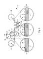
- FIG. 4a reverse gravure printing apparatus 31 is shown.
- a sheet 32 of metallised filmis wrapped around an unwind roller 33 .
- the sheet 32comprises the substrate 34 supporting a thin layer 35 of metallisation, in this case aluminium, on one side 36 .
- the sheet 32is paid out from the roller 33 and is passed between a first gravure cylinder 37 and a corresponding counter impression roller 38 , which is used to apply a dielectric solution 39 from source 40 over the metallisation 35 .
- the solution 39dries or is cured, for example using ultraviolet light, to leave a dielectric layer 41 on the sheet 33 .
- the sheet 32is then passed between a second gravure cylinder 42 and a corresponding counter impression roller 43 , which is used to apply an organic semiconductor solution 44 from source 45 over the dielectric layer 41 .
- the organic semiconductor solution 42dries or is cured to form an organic semiconductor layer 46 .
- the dielectric solution 39may comprise poly(4-vinyl phenol) (Sigma-Aldrich) dissolved in a suitable solvent, such as isopropyl alcohol (“IPA”).
- the organic semiconductor solution 44may comprise poly(3-hexylthiophene) (Sigma-Aldrich) dissolved in a suitable solvent, such as chloroform or xylene.
- Each solution 39 , 41may include two or more different solvents and/or may include additive(s) to provide a solution which suitable for printing, e.g. having appropriate viscosity.
- the printing processproduces a laminated sheet 47 including a multiple layer structure 48 comprising the metallisation layer 35 , the dielectric layer 41 and the organic semiconductor layer 46 .
- the laminate sheet 47is wound onto a re-wind roller 49 .
- This processcan be used to form layers 35 , 41 , 46 which are thin (e.g. less than 500 nm thick) and high quality, namely substantially free of pin holes and contamination.
- the patterned sheet 28 ( FIG. 3 ) and laminate sheet 47 ( FIG. 4 )are used to fabricate the transistor 1 ( FIG. 1 ) in a fast roll-to-roll process using a stamping process.
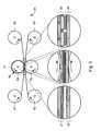
- a layer transferring apparatus 51is shown.
- stamping apparatusis used.
- the patterned sheet 28 and the laminate sheet 47are wrapped around first and second rollers respectively 52 , 53 .
- the sheets 28 , 47are paid out with the layer structure 48 and the electrodes 5 , 6 facing each other and are passed through a stamp comprising a patterning roller 54 and an impression roller 55 .
- An outer surface 56 of the patterning roller 54carries a plate 57 defining an image of the gate electrode 10 ( FIG. 1 ).
- the patterning roller 54stamps selected regions 58 of the layer structure 48 from the first sheet 47 over the electrodes 5 , 6 onto the second sheet 48 .
- Cold stamping or hot stampingmay be used.
- the patterning roller 54is heated to more than about 300° C.
- the transfer processneed not use stamping, e.g. to apply high pressure to transfer layer structures.
- selected regions 58may be transferred by applying merely kissing pressure.
- Selected regions 58may be transferred by pulling the regions from the layer structure 48 , for example by virtue of surface tension.
- a sheet 59 carrying the transistor 1 having and another spent laminate sheet 60are wound onto respective rollers 61 , 62 .
- the stamping processis continuous and can be used to form large numbers of transistors 1 or other types of devices, such as interconnects and sensors, simultaneously.
- the sheet 59is processed further to interconnect transistors and/or other devices and a further stamping process can be used to deposit a layer structure comprising a single layer of conducting material so as to provide interconnects.
- the layer structure in the laminatemay have only one layer or may have more than one layer.
- the devicemay be other forms of electronic device such as a battery, sensor or organic light emitting diode.
- the devicemay be based on electron and/or hole transport.
- the semiconductormay be an organic semiconductor such as be poly3-benzothiazolyl thiophene (“PBTT”) or dioctylfluorene-bithiophene (“F8T2”)
- PBTTpoly3-benzothiazolyl thiophene
- F8T2dioctylfluorene-bithiophene
- the methodmay be used to fabricate devices having a bottom gate structure.
- the processmay be sheet fed and so stages, such as stamping, may be board-based rather than cylinder-based.
Landscapes
- Engineering & Computer Science (AREA)
- Manufacturing & Machinery (AREA)
- Thin Film Transistor (AREA)
Abstract
Description
- The present invention relates to a method of fabricating an electronic device, particularly, but not exclusively, an organic thin film transistor.
- Organic thin film transistors can be fabricated using well-known thin film deposition and patterning processes, such as evaporation, sputtering, spin coating, optical lithography and etching. Usually during fabrication, thin films of material are deposited and patterned in separate steps. This allows a manufacturer to control film quality and feature size independently and so maximise film quality and minimise feature sizes. However, many of these thin film processes are not particularly suited to fabricating transistors at low cost and in high volumes.
- To address this problem, organic thin film transistors can also be fabricated using printing processes, such as ink jet printing. However, this usually results in a drop in film quality and/or rise in minimum feature size.
- The present invention seeks to provide an improved method of fabricating an electronic device.
- According to a first aspect of the present invention there is provided a method of fabricating an electronic device comprising providing a layer structure supported on a first substrate, providing a second, patterned substrate and transferring selected areas of the first layer structure onto the second substrate.
- This can be used to enjoy the benefits of being able to prepare high quality films and of being able to fabricate devices using a high-throughput process.
- The layer structure may include at least one conductive layer, at least one insulating layer and/or at least one semiconducting layer. The layers may be co-extensive. The first substrate may be a sheet.
- The second, patterned substrate may comprise electrically conductive regions supported on a sheet.
- The electronic device may be an organic thin film transistor. The patterned substrate may include source and drain electrodes and the layer structure may comprise a gate metallisation layer, a gate insulating layer and a semiconducting layer.
- Transferring the selected areas of the first layer structure onto the second substrate may comprise transferring all of the first layer structure across the extent of the electronic device or even all of the first layer structure.
- Transferring the selected areas of the first layer structure onto the second substrate may comprise stamping the layer structure from the first layer structure.
- Stamping may comprise heating a stamp to at least 300° C.
- The method may comprise forming the layer structure on the first substrate by depositing a first layer on the substrate. Depositing the first layer may comprise evaporating or printing the first layer onto the substrate. The method may further comprise depositing a second layer over the first layer. Depositing the second layer may comprise printing the second layer onto the first layer. The method may further comprise depositing a third layer over the second layer. Depositing the third layer may comprise printing the third layer onto the second layer.
- The method may comprises forming the patterned substrate by etching regions of a layer structure to form a patterned layer structure on a substrate or by depositing a patterned layer structure onto a substrate. The layer structure may comprise a single layer.
- According to a second aspect of the present invention there is provided a device fabricated by the method.
- According to a third aspect of the present invention there is provided apparatus for fabricating an electronic device comprising means for providing a layer structure supported on a first substrate, means for providing a second, patterned substrate; and means for transferring selected areas of the first layer structure onto the second substrate.
- The means for providing the layer structure may comprise means for depositing a metallic layer on the substrate. The means for providing the layer structure may comprise printing apparatus, such as gravure printing apparatus.
- The means for providing a second, patterned substrate may comprise printing apparatus.
- The means for transferring selected areas from the first layer structure onto the second substrate may comprise a stamp. The stamp may be provided on a cylinder.
- Embodiments of the present invention will now be described, by way of example, with reference to the accompanying drawings in which:
FIG. 1 is a plan view of an organic thin film transistor;FIG. 2 is a cross-sectional view of the transistor shown inFIG. 1 ;FIG. 3 is a schematic diagram showing a process of fabricating a patterned substrate;FIG. 4 is a schematic diagram showing a process of fabricating a laminate; andFIG. 5 is a schematic diagram showing a process of fabricating the organic transistor shown inFIG. 1 in accordance with the present invention.- Referring to
FIGS. 1 and 2 , athin film transistor 1 in accordance with the present invention is shown. Thethin film transistor 1 comprises aflexible substrate 2 formed from a plastic material, such as polyethylene terephthalate (PET). Thesubstrate 2 supports a “top gate, bottom electrode”transistor structure 3 on a first surface4 (hereinafter referred to as “the upper face”). - The
substrate 2 supports source anddrain electrodes upper surface 4. A patternedlayer 7 of an organic semiconductor, such as poly(3-hexylthiophene) (“P3HT”), lies over thesubstrate 2 and the source anddrain electrodes drain electrodes layer 9 of insulating material, such as poly(4-vinyl phenol) (“PVP”), lies over theorganic semiconductor layer 7 to form a gate dielectric and agate electrode 10 formed from a metal, such as aluminium, or metal alloy lies over the gate dielectric9. - Referring in particular to
FIG. 1 , the source anddrain electrodes FIG. 1 , the source anddrain electrodes FIG. 1 , theorganic semiconductor layer 7,dielectric layer 9 andgate electrode 10 are co-extensive. - Referring in particular to
FIG. 2 , the source anddrain electrodes organic semiconductor layer 7 has a thickness, t2, of about 100 nm. The gate dielectric8 has a thickness, t3, of about 1 μm and thegate electrode 10 has a thickness of about 40 nm. - Referring to
FIGS. 3 to 5 , apparatus for and a method of fabricating thethin film transistor 1 shown inFIGS. 1 and 2 in accordance with the present invention will now be described. - Referring in particular to
FIG. 3 , aflexographic printing apparatus 11 is shown. - A sheet12 (or “web”) of metallised film is wrapped around an
unwind roller 13. Thesheet 12 comprises asubstrate 2, which will eventually form the substrate for the transistor1 (FIG. 1 ), and athin layer 14 of metallisation, in this case aluminium, supported on oneside 4. Themetallisation 14 can be applied to thesubstrate 2 using a moving vacuum metallisation process (not shown), at speeds of up to 60 km/hr. - The
sheet 12 is paid out from theunwind roller 13 and passed between aprinting roller 15 and animpression roller 16 providing support. Anouter surface 17 of theprinting roller 15 carries a printing plate orscreen 18 defining an image of the source anddrain electrodes 5,6 (FIG. 1 ). The surface of the metallised sheet may be treated, e.g. using corona discharge, to improve adhesion. Theprinting roller 15 co-operates with ananilox roller 19 which is used to apply a measured amount ofink 20 from asource 21 so as to produce anink pattern 22 which provides an etch mask on themetallisation layer 14. Theink 20 may comprise Microposit S1813 photoresist (Rohm & Haas) or other suitable mixtures of polymers dissolved in, for example non-aqueous, solvent and which is suitable for printing. The resist may be heated, e.g. to reduce pin holes. Themasked metallised sheet 13′ passes through afirst bath 23 containing awet etch 24 which etches unmaskedareas 25 ofmetallisation 14 and then through asecond bath 26 containing a rinse27 to remove theetch mask 22. Thewet etch 24 for aluminium may be an aqueous solution of phosphoric acid, acetic acid and nitric acid (Microchem Systems Ltd) or aqueous sodium hydroxide. The rinse27 may be Microposit1165 photoresist remover (Rohm & Haas). This leaves apatterned sheet 28 comprising thesubstrate 2 and patterned regions of metallisation, namely the source anddrain electrodes sheet 28 is wound onto are-wind roller 29. - The process can be run at high speeds, e.g. 60 m/min, and has an advantage that the printing process is not used to apply a conductive ink and so can be optimised for print resolution without needing to take into account loading the ink with conductive particles. The etching process is quick, typically taking about 1 s to etch through the
metallisation layer 14. - The
printing plate 18 is formed by laser ablation and can form images with a resolution of about 10 μm and can even reach resolutions of about 5 μm. - Other forms of coating or printing can be used, such as gravure.
- Referring now to
FIG. 4 , a reversegravure printing apparatus 31 is shown. - A
sheet 32 of metallised film is wrapped around an unwindroller 33. Thesheet 32 comprises thesubstrate 34 supporting athin layer 35 of metallisation, in this case aluminium, on oneside 36. - The
sheet 32 is paid out from theroller 33 and is passed between afirst gravure cylinder 37 and a correspondingcounter impression roller 38, which is used to apply adielectric solution 39 fromsource 40 over themetallisation 35. Thesolution 39 dries or is cured, for example using ultraviolet light, to leave adielectric layer 41 on thesheet 33. Thesheet 32 is then passed between asecond gravure cylinder 42 and a correspondingcounter impression roller 43, which is used to apply anorganic semiconductor solution 44 fromsource 45 over thedielectric layer 41. Theorganic semiconductor solution 42 dries or is cured to form anorganic semiconductor layer 46. - The
dielectric solution 39 may comprise poly(4-vinyl phenol) (Sigma-Aldrich) dissolved in a suitable solvent, such as isopropyl alcohol (“IPA”). Theorganic semiconductor solution 44 may comprise poly(3-hexylthiophene) (Sigma-Aldrich) dissolved in a suitable solvent, such as chloroform or xylene. Eachsolution - The printing process produces a
laminated sheet 47 including amultiple layer structure 48 comprising themetallisation layer 35, thedielectric layer 41 and theorganic semiconductor layer 46. Thelaminate sheet 47 is wound onto are-wind roller 49. - This process can be used to form
layers - Other forms of coating or printing can be used, such as gravure and spray coating.
- The patterned sheet28 (
FIG. 3 ) and laminate sheet47 (FIG. 4 ) are used to fabricate the transistor1 (FIG. 1 ) in a fast roll-to-roll process using a stamping process. - Referring to
FIG. 5 , alayer transferring apparatus 51 is shown. In this example, stamping apparatus is used. - The patterned
sheet 28 and thelaminate sheet 47 are wrapped around first and second rollers respectively52,53. - The
sheets layer structure 48 and theelectrodes patterning roller 54 and animpression roller 55. Anouter surface 56 of thepatterning roller 54 carries aplate 57 defining an image of the gate electrode10 (FIG. 1 ). Thepatterning roller 54 stamps selected regions58 of thelayer structure 48 from thefirst sheet 47 over theelectrodes second sheet 48. Cold stamping or hot stamping may be used. For hot stamping, thepatterning roller 54 is heated to more than about 300° C. - The transfer process need not use stamping, e.g. to apply high pressure to transfer layer structures. For example, selected regions58 may be transferred by applying merely kissing pressure. Selected regions58 may be transferred by pulling the regions from the
layer structure 48, for example by virtue of surface tension. - A
sheet 59 carrying thetransistor 1 having and another spentlaminate sheet 60 are wound ontorespective rollers - The stamping process is continuous and can be used to form large numbers of
transistors 1 or other types of devices, such as interconnects and sensors, simultaneously. - The
sheet 59 is processed further to interconnect transistors and/or other devices and a further stamping process can be used to deposit a layer structure comprising a single layer of conducting material so as to provide interconnects. - It will be appreciated that many modifications may be made to the embodiments hereinbefore described.
- For example, the layer structure in the laminate may have only one layer or may have more than one layer.
- The device may be other forms of electronic device such as a battery, sensor or organic light emitting diode. The device may be based on electron and/or hole transport.
- The semiconductor may be an organic semiconductor such as be poly3-benzothiazolyl thiophene (“PBTT”) or dioctylfluorene-bithiophene (“F8T2”)
- The method may be used to fabricate devices having a bottom gate structure.
- The process may be sheet fed and so stages, such as stamping, may be board-based rather than cylinder-based.
Claims (30)
1. A method of fabricating an electronic device comprising:
providing a layer structure supported on a first substrate;
providing a second, patterned substrate; and
transferring selected areas of the layer structure onto the second substrate.
2. A method according toclaim 1 , wherein the layer structure includes at least one conductive layer.
3. A method according toclaim 1 , wherein the layer structure includes at least one insulating layer.
4. A method according toclaim 1 , wherein the layer structure includes at least one semiconducting layer.
5. A method according toclaim 1 , wherein the second, patterned substrate comprises electrically conductive regions supported on a sheet.
6. A method according toclaim 1 , wherein the electronic device is an organic thin film transistor.
7. A method according toclaim 1 , wherein the patterned substrate carries source and drain electrodes and the layer structure comprises a gate metallisation layer, a gate insulating layer and a semiconducting layer.
8. A method according toclaim 1 , wherein transferring the selected areas of the layer structure onto the second substrate comprises transferring all of the layer structure across the extent of the electronic device.
9. A method according toclaim 1 , wherein transferring the selected areas of the layer structure onto the second substrate comprises transferring all of the layer structure.
10. A method according toclaim 1 , wherein transferring the selected areas of the layer structure onto the second substrate comprises stamping the layer structure from the first substrate onto the second substrate.
11. A method according toclaim 10 , wherein stamping comprises heating a stamp to at least 300° C.
12. A method according toclaim 1 , comprising:
forming the layer structure on the first substrate by depositing a first layer on the substrate.
13. A method according toclaim 12 , wherein depositing the first layer comprises evaporating the first layer onto the substrate.
14. A method according toclaim 12 , wherein depositing the first layer comprises printing the first layer onto the substrate.
15. A method according toclaim 12 , further comprising depositing a second layer over the first layer.
16. A method according toclaim 15 , wherein depositing the second layer comprises printing the second layer onto the first layer.
17. A method according toclaim 15 , further comprising depositing a third layer over the second layer.
18. A method according toclaim 17 , wherein depositing the third layer comprises printing the third layer onto the second layer.
19. A method according toclaim 1 , comprising:
forming the patterned substrate by etching regions of a layer structure to form a patterned layer structure on a substrate.
20. A method according toclaim 1 , comprising:
forming the patterned substrate by depositing a patterned layer structure onto a substrate.
21. A method according toclaim 19 , wherein the layer structure comprises a single layer.
22. A method according toclaim 1 , wherein the layer structure is dry.
23. A device fabricated by a method according toclaim 1 .
24. Apparatus for fabricating an electronic device comprising:
means for providing a layer structure supported on a first substrate;
means for providing a second, patterned substrate; and
means for transferring selected areas of the layer structure onto the second substrate.
25. Apparatus according toclaim 24 , wherein the means for providing the layer structure comprises means for depositing a metallic layer on a substrate.
26. Apparatus according toclaim 24 , wherein the means for providing the layer structure comprises printing apparatus.
27. Apparatus according toclaim 26 , wherein the printing apparatus comprises gravure printing apparatus.
28. Apparatus according toclaim 24 , wherein the means for providing a second, patterned substrate comprises printing apparatus.
29. Apparatus according toclaim 24 , wherein means for transferring selected areas from the first layer structure onto the second substrate comprises a stamp.
30. Apparatus according toclaim 29 , wherein the stamp is provided on a cylinder.
Applications Claiming Priority (3)
| Application Number | Priority Date | Filing Date | Title |
|---|---|---|---|
| GB0720392AGB2453766A (en) | 2007-10-18 | 2007-10-18 | Method of fabricating an electronic device |
| GB0720392.0 | 2007-10-18 | ||
| PCT/GB2008/050950WO2009050516A1 (en) | 2007-10-18 | 2008-10-17 | Method of fabricating an electronic device |
Publications (2)
| Publication Number | Publication Date |
|---|---|
| US20100295028A1true US20100295028A1 (en) | 2010-11-25 |
| US8969127B2 US8969127B2 (en) | 2015-03-03 |
Family
ID=38814056
Family Applications (1)
| Application Number | Title | Priority Date | Filing Date |
|---|---|---|---|
| US12/738,173Active2030-05-05US8969127B2 (en) | 2007-10-18 | 2008-10-17 | Apparatus for and method of fabricating an electronic device by transfer of material onto a substrate |
Country Status (4)
| Country | Link |
|---|---|
| US (1) | US8969127B2 (en) |
| EP (1) | EP2206171B1 (en) |
| GB (1) | GB2453766A (en) |
| WO (1) | WO2009050516A1 (en) |
Cited By (1)
| Publication number | Priority date | Publication date | Assignee | Title |
|---|---|---|---|---|
| US20150187895A1 (en)* | 2013-12-31 | 2015-07-02 | Au Optronics Corp. | Thin film transistor structure |
Families Citing this family (3)
| Publication number | Priority date | Publication date | Assignee | Title |
|---|---|---|---|---|
| GB2453766A (en) | 2007-10-18 | 2009-04-22 | Novalia Ltd | Method of fabricating an electronic device |
| DE102010040059A1 (en)* | 2010-08-31 | 2012-03-01 | Von Ardenne Anlagentechnik Gmbh | Strip or sheet-shaped substrate e.g. metal strip, temperature controlling method for use during manufacturing e.g. organic LED, involves arranging carrier in heat transfer region between control device and substrate, and moving carrier |
| US9679946B2 (en)* | 2014-08-25 | 2017-06-13 | HGST, Inc. | 3-D planes memory device |
Citations (79)
| Publication number | Priority date | Publication date | Assignee | Title |
|---|---|---|---|---|
| US4400409A (en)* | 1980-05-19 | 1983-08-23 | Energy Conversion Devices, Inc. | Method of making p-doped silicon films |
| US4677738A (en)* | 1980-05-19 | 1987-07-07 | Energy Conversion Devices, Inc. | Method of making a photovoltaic panel |
| US5512131A (en)* | 1993-10-04 | 1996-04-30 | President And Fellows Of Harvard College | Formation of microstamped patterns on surfaces and derivative articles |
| US5707745A (en)* | 1994-12-13 | 1998-01-13 | The Trustees Of Princeton University | Multicolor organic light emitting devices |
| US5776748A (en)* | 1993-10-04 | 1998-07-07 | President And Fellows Of Harvard College | Method of formation of microstamped patterns on plates for adhesion of cells and other biological materials, devices and uses therefor |
| US5817242A (en)* | 1995-08-04 | 1998-10-06 | International Business Machines Corporation | Stamp for a lithographic process |
| US5937758A (en)* | 1997-11-26 | 1999-08-17 | Motorola, Inc. | Micro-contact printing stamp |
| US5976257A (en)* | 1991-01-23 | 1999-11-02 | Canon Kabushiki Kaisha | Apparatus for continuously forming a large area deposited film by means of microwave plasma CVD process |
| US6027595A (en)* | 1998-07-02 | 2000-02-22 | Samsung Electronics Co., Ltd. | Method of making optical replicas by stamping in photoresist and replicas formed thereby |
| US6096389A (en)* | 1995-09-14 | 2000-08-01 | Canon Kabushiki Kaisha | Method and apparatus for forming a deposited film using a microwave CVD process |
| US6143991A (en)* | 1995-05-26 | 2000-11-07 | Nec Corporation | Bump electrode with adjacent pad and insulation for solder flow stopping |
| US6180239B1 (en)* | 1993-10-04 | 2001-01-30 | President And Fellows Of Harvard College | Microcontact printing on surfaces and derivative articles |
| US6309580B1 (en)* | 1995-11-15 | 2001-10-30 | Regents Of The University Of Minnesota | Release surfaces, particularly for use in nanoimprint lithography |
| US6380101B1 (en)* | 2000-04-18 | 2002-04-30 | International Business Machines Corporation | Method of forming patterned indium zinc oxide and indium tin oxide films via microcontact printing and uses thereof |
| US20020197554A1 (en)* | 1999-01-15 | 2002-12-26 | 3M Innovative Properties Company | Thermal transfer element and process for forming organic electroluminescent devices |
| US6518168B1 (en)* | 1995-08-18 | 2003-02-11 | President And Fellows Of Harvard College | Self-assembled monolayer directed patterning of surfaces |
| US20030057601A1 (en)* | 2001-04-19 | 2003-03-27 | Reitz John Bradford | Methods for embossing and embossed articles formed therby |
| US20030173890A1 (en)* | 2002-03-14 | 2003-09-18 | Semiconductor Energy Laboratory Co., Ltd. | Display device and method of fabricating the same |
| US6645573B2 (en)* | 1998-03-03 | 2003-11-11 | Canon Kabushiki Kaisha | Process for forming a microcrystalline silicon series thin film and apparatus suitable for practicing said process |
| US6673287B2 (en)* | 2001-05-16 | 2004-01-06 | International Business Machines Corporation | Vapor phase surface modification of composite substrates to form a molecularly thin release layer |
| US6726812B1 (en)* | 1997-03-04 | 2004-04-27 | Canon Kabushiki Kaisha | Ion beam sputtering apparatus, method for forming a transparent and electrically conductive film, and process for the production of a semiconductor device |
| US20040121568A1 (en)* | 2002-12-20 | 2004-06-24 | Changsoon Kim | Methods of fabricating devices by low pressure cold welding |
| US6780492B2 (en)* | 1999-03-02 | 2004-08-24 | International Business Machines Corporation | Substrates prepared by chemical amplification of self-assembled monolayers with spatially localized polymer brushes |
| US6792856B2 (en)* | 2002-07-16 | 2004-09-21 | International Business Machines Corporation | Method and apparatus for accurate, micro-contact printing |
| US20040187917A1 (en)* | 2003-03-29 | 2004-09-30 | Nanosolar, Inc. | Transparent electrode, optoelectronic apparatus and devices |
| US6811816B2 (en)* | 2000-05-01 | 2004-11-02 | Canon Kabushiki Kaisha | Method and apparatus for forming deposition film, and method for treating substrate |
| US20040231781A1 (en)* | 2003-05-23 | 2004-11-25 | Agency For Science, Technology And Research | Methods of creating patterns on substrates and articles of manufacture resulting therefrom |
| US20050009327A1 (en)* | 2003-05-13 | 2005-01-13 | Yoshihiro Yoshida | Apparatus and method for formation of a wiring pattern on a substrate, and electronic devices and producing methods thereof |
| US6858087B2 (en)* | 2000-01-31 | 2005-02-22 | Canon Kabushiki Kaisha | Vacuum-processing method using a movable cooling plate during processing |
| US6887332B1 (en)* | 2000-04-21 | 2005-05-03 | International Business Machines Corporation | Patterning solution deposited thin films with self-assembled monolayers |
| US20050170621A1 (en)* | 2002-12-20 | 2005-08-04 | Changsoon Kim | Methods of fabricating devices by transfer of organic material |
| US20050173701A1 (en)* | 2004-02-09 | 2005-08-11 | Seiko Epson Corporation | Transistor, circuit board, display and electronic equipment |
| US6946597B2 (en)* | 2002-06-22 | 2005-09-20 | Nanosular, Inc. | Photovoltaic devices fabricated by growth from porous template |
| US20050233491A1 (en)* | 2004-03-31 | 2005-10-20 | Konica Minolta Holdings, Inc. | Thin-film transistor sheet and manufacturing method thereof |
| US20050244990A1 (en)* | 2004-04-30 | 2005-11-03 | Lg. Philips Lcd Co., Ltd. | Method for forming pattern using printing method |
| US20050268962A1 (en)* | 2000-04-27 | 2005-12-08 | Russell Gaudiana | Flexible Photovoltaic cells, systems and methods |
| US20050274541A1 (en)* | 1998-12-14 | 2005-12-15 | Norio Takahashi | Module circuit board for semiconductor device having barriers to isolate I/O terminals from solder |
| US20060110545A1 (en)* | 2004-11-25 | 2006-05-25 | Seiko Epson Corporation | Method of forming conductive pattern |
| US7061010B2 (en)* | 2001-08-09 | 2006-06-13 | Asahi Kasei Kabushiki Kaisha | Organic semiconductor element |
| US20060134841A1 (en)* | 2004-12-17 | 2006-06-22 | Lg Philips Lcd Co., Ltd. | Method of forming pattern having step difference and method of making thin film transistor and liquid crystal display using the same |
| US7071081B2 (en)* | 2003-05-07 | 2006-07-04 | Canon Kabushiki Kaisha | Method of forming semiconductor device |
| US20060196377A1 (en)* | 2005-03-07 | 2006-09-07 | Asml Netherlands B.V. | Imprint lithography |
| US7117790B2 (en)* | 2002-01-11 | 2006-10-10 | Massachusetts Institute Of Technology | Microcontact printing |
| US20060254440A1 (en)* | 2005-04-13 | 2006-11-16 | Korea Institute Of Machinery & Materials | Method and apparatus for manufacturing electronic device using roll-to-roll rotary pressing process |
| US20070009827A1 (en)* | 2003-05-23 | 2007-01-11 | Intelleflex Corporation | Lamination and delamination technique for thin film processing |
| US20070020821A1 (en)* | 2005-07-25 | 2007-01-25 | Seiko Epson Corporation | Method for forming a thin-film transistor |
| US20070056680A1 (en)* | 2003-05-23 | 2007-03-15 | The Regents Of The University Of Michigan | Imprinting polymer film on patterned substrate |
| US7195733B2 (en)* | 2004-04-27 | 2007-03-27 | The Board Of Trustees Of The University Of Illinois | Composite patterning devices for soft lithography |
| US7202007B2 (en)* | 2002-06-07 | 2007-04-10 | Fujifilm Corporation | Method of forming patterned films |
| US20070104879A1 (en)* | 2001-10-05 | 2007-05-10 | Cabot Corporation | Low viscosity precursor compositions and methods for the deposition of conductive electronic features |
| US20070145632A1 (en)* | 2003-10-11 | 2007-06-28 | Koninklijke Philips Electronics N.C. | Elastomeric stamp, patterning method using such a stamp and method for producing such a stamp |
| US20070184198A1 (en)* | 2006-02-07 | 2007-08-09 | Fmc Corporation | Coating process to produce controlled release coatings |
| US20070181059A1 (en)* | 2000-04-21 | 2007-08-09 | Lee Jae Y | Apparatus and method for patterning pixels of an electro-luminescent display device |
| US20070200489A1 (en)* | 2006-02-01 | 2007-08-30 | Poon Hak F | Large area organic electronic devices and methods of fabricating the same |
| US20070215869A1 (en)* | 2004-12-07 | 2007-09-20 | Semiconductor Energy Laboratory Co., Ltd. | Semiconductor Device and Method for Manufacturing the Same |
| US7296519B2 (en)* | 2002-05-27 | 2007-11-20 | Koninklijke Philips Electronics N.V. | Method and device for transferring a pattern from stamp to a substrate |
| US20080012006A1 (en)* | 2006-07-17 | 2008-01-17 | Richard Kevin Bailey | Thin film transistor comprising novel conductor and dielectric compositions |
| US20080047930A1 (en)* | 2006-08-23 | 2008-02-28 | Graciela Beatriz Blanchet | Method to form a pattern of functional material on a substrate |
| US20080055581A1 (en)* | 2004-04-27 | 2008-03-06 | Rogers John A | Devices and methods for pattern generation by ink lithography |
| US20080076205A1 (en)* | 2006-09-22 | 2008-03-27 | Konica Minolta Holdings, Inc. | Donor sheet and method of manufacturing donor sheet and organic thin film transistor |
| US20080083484A1 (en)* | 2006-09-28 | 2008-04-10 | Graciela Beatriz Blanchet | Method to form a pattern of functional material on a substrate |
| US7363854B2 (en)* | 2004-12-16 | 2008-04-29 | Asml Holding N.V. | System and method for patterning both sides of a substrate utilizing imprint lithography |
| US20080227232A1 (en)* | 2006-07-28 | 2008-09-18 | Semiconductor Energy Laboratory Co., Ltd. | Method for manufacturing display device |
| US20080245248A1 (en)* | 2007-04-09 | 2008-10-09 | Nec Lcd Technologies, Ltd. | Printing method, printing apparatus and liquid-crystal display device using the same |
| US20080289524A1 (en)* | 2004-10-22 | 2008-11-27 | Koninklijke Philips Electronics, N.V. | Roller Micro-Contact Printer with Pressure Control |
| US7462244B2 (en)* | 2001-11-27 | 2008-12-09 | Nec Corporation | Device and method for vacuum film formation |
| US7514342B2 (en)* | 2004-05-24 | 2009-04-07 | Canon Kabushiki Kaisha | Method and apparatus for forming deposited film |
| US7557367B2 (en)* | 2004-06-04 | 2009-07-07 | The Board Of Trustees Of The University Of Illinois | Stretchable semiconductor elements and stretchable electrical circuits |
| US20090199960A1 (en)* | 2004-06-04 | 2009-08-13 | Nuzzo Ralph G | Pattern Transfer Printing by Kinetic Control of Adhesion to an Elastomeric Stamp |
| US7588657B2 (en)* | 2003-09-29 | 2009-09-15 | Princeton University | Pattern-free method of making line gratings |
| US7682981B2 (en)* | 2005-01-27 | 2010-03-23 | Contour Semiconductor, Inc. | Topography transfer method with aspect ratio scaling |
| US7777128B2 (en)* | 2004-06-01 | 2010-08-17 | Konarka Technologies, Inc. | Photovoltaic module architecture |
| US7802517B2 (en)* | 2005-11-02 | 2010-09-28 | Sony Deutschland Gmbh | Method of patterning molecules on a substrate using a micro-contact printing process |
| US7803308B2 (en)* | 2005-12-01 | 2010-09-28 | Molecular Imprints, Inc. | Technique for separating a mold from solidified imprinting material |
| US20100261321A1 (en)* | 2008-08-04 | 2010-10-14 | Koichi Hirano | Method for manufacturing flexible semiconductor device |
| US7825406B2 (en)* | 2007-05-31 | 2010-11-02 | Panasonic Corporation | Organic EL device |
| US7852435B2 (en)* | 2004-07-16 | 2010-12-14 | Kuraray Co., Ltd. | Light-condensing film, liquid-crystal panel and backlight as well as manufacturing process for light-condensing film |
| US7968804B2 (en)* | 2006-12-20 | 2011-06-28 | 3M Innovative Properties Company | Methods of patterning a deposit metal on a substrate |
| US8557351B2 (en)* | 2005-07-22 | 2013-10-15 | Molecular Imprints, Inc. | Method for adhering materials together |
Family Cites Families (14)
| Publication number | Priority date | Publication date | Assignee | Title |
|---|---|---|---|---|
| JPH07283493A (en) | 1994-04-14 | 1995-10-27 | Nippon Chemicon Corp | Circuit board with function for preventing flux residue sticking |
| JP2003187972A (en)* | 2001-12-20 | 2003-07-04 | Dainippon Printing Co Ltd | Method for manufacturing organic EL element and organic EL transfer member and transfer object |
| US20050252602A1 (en)* | 2002-03-20 | 2005-11-17 | Tomomi Tateishi | Organic thin-film device and its production method |
| EP1354638A3 (en)* | 2002-04-15 | 2004-11-03 | Fuji Photo Film Co., Ltd. | Method and apparatus for manufacturing pattern members using webs on which coating films have been formed |
| JP3867659B2 (en)* | 2002-11-26 | 2007-01-10 | ソニー株式会社 | Method for manufacturing organic electroluminescent device |
| US6918982B2 (en)* | 2002-12-09 | 2005-07-19 | International Business Machines Corporation | System and method of transfer printing an organic semiconductor |
| KR20050109604A (en)* | 2003-03-27 | 2005-11-21 | 이 아이 듀폰 디 네모아 앤드 캄파니 | Processes and donor elements for transferring thermally sensitive materials to substrates |
| US7105462B2 (en)* | 2003-07-22 | 2006-09-12 | E. I. Du Pont De Nemours And Company | Lamination of organic semiconductor |
| KR20060102329A (en)* | 2003-09-26 | 2006-09-27 | 이 아이 듀폰 디 네모아 앤드 캄파니 | Lamination through Mask |
| DE10349963A1 (en)* | 2003-10-24 | 2005-06-02 | Leonhard Kurz Gmbh & Co. Kg | Process for producing a film |
| JP4402964B2 (en)* | 2004-01-14 | 2010-01-20 | 富士フイルム株式会社 | Pattern film forming method |
| DE102004005370B4 (en) | 2004-02-03 | 2007-08-16 | Samsung SDI Co., Ltd., Suwon | Electrical device with a housing and an OLED display element and method for its production |
| KR101223718B1 (en)* | 2005-06-18 | 2013-01-18 | 삼성디스플레이 주식회사 | Method for patterning nano conductive film |
| GB2453766A (en) | 2007-10-18 | 2009-04-22 | Novalia Ltd | Method of fabricating an electronic device |
- 2007
- 2007-10-18GBGB0720392Apatent/GB2453766A/ennot_activeWithdrawn
- 2008
- 2008-10-17EPEP08806764.0Apatent/EP2206171B1/ennot_activeNot-in-force
- 2008-10-17WOPCT/GB2008/050950patent/WO2009050516A1/enactiveApplication Filing
- 2008-10-17USUS12/738,173patent/US8969127B2/enactiveActive
Patent Citations (87)
| Publication number | Priority date | Publication date | Assignee | Title |
|---|---|---|---|---|
| US4677738A (en)* | 1980-05-19 | 1987-07-07 | Energy Conversion Devices, Inc. | Method of making a photovoltaic panel |
| US4400409A (en)* | 1980-05-19 | 1983-08-23 | Energy Conversion Devices, Inc. | Method of making p-doped silicon films |
| US5976257A (en)* | 1991-01-23 | 1999-11-02 | Canon Kabushiki Kaisha | Apparatus for continuously forming a large area deposited film by means of microwave plasma CVD process |
| US6368838B1 (en)* | 1993-10-04 | 2002-04-09 | President And Fellows Of Havard College | Adhering cells to cytophilic islands separated by cytophobic regions to form patterns and manipulate cells |
| US5512131A (en)* | 1993-10-04 | 1996-04-30 | President And Fellows Of Harvard College | Formation of microstamped patterns on surfaces and derivative articles |
| US5976826A (en)* | 1993-10-04 | 1999-11-02 | President And Fellows Of Harvard College | Device containing cytophilic islands that adhere cells separated by cytophobic regions |
| US7067306B2 (en)* | 1993-10-04 | 2006-06-27 | President & Fellows Of Harvard College | Device containing cytophilic islands that adhere cells separated by cytophobic regions |
| US6180239B1 (en)* | 1993-10-04 | 2001-01-30 | President And Fellows Of Harvard College | Microcontact printing on surfaces and derivative articles |
| US5776748A (en)* | 1993-10-04 | 1998-07-07 | President And Fellows Of Harvard College | Method of formation of microstamped patterns on plates for adhesion of cells and other biological materials, devices and uses therefor |
| US5707745A (en)* | 1994-12-13 | 1998-01-13 | The Trustees Of Princeton University | Multicolor organic light emitting devices |
| US6143991A (en)* | 1995-05-26 | 2000-11-07 | Nec Corporation | Bump electrode with adjacent pad and insulation for solder flow stopping |
| US5817242A (en)* | 1995-08-04 | 1998-10-06 | International Business Machines Corporation | Stamp for a lithographic process |
| US6518168B1 (en)* | 1995-08-18 | 2003-02-11 | President And Fellows Of Harvard College | Self-assembled monolayer directed patterning of surfaces |
| US6096389A (en)* | 1995-09-14 | 2000-08-01 | Canon Kabushiki Kaisha | Method and apparatus for forming a deposited film using a microwave CVD process |
| US6309580B1 (en)* | 1995-11-15 | 2001-10-30 | Regents Of The University Of Minnesota | Release surfaces, particularly for use in nanoimprint lithography |
| US6726812B1 (en)* | 1997-03-04 | 2004-04-27 | Canon Kabushiki Kaisha | Ion beam sputtering apparatus, method for forming a transparent and electrically conductive film, and process for the production of a semiconductor device |
| US5937758A (en)* | 1997-11-26 | 1999-08-17 | Motorola, Inc. | Micro-contact printing stamp |
| US6645573B2 (en)* | 1998-03-03 | 2003-11-11 | Canon Kabushiki Kaisha | Process for forming a microcrystalline silicon series thin film and apparatus suitable for practicing said process |
| US6027595A (en)* | 1998-07-02 | 2000-02-22 | Samsung Electronics Co., Ltd. | Method of making optical replicas by stamping in photoresist and replicas formed thereby |
| US20050274541A1 (en)* | 1998-12-14 | 2005-12-15 | Norio Takahashi | Module circuit board for semiconductor device having barriers to isolate I/O terminals from solder |
| US20020197554A1 (en)* | 1999-01-15 | 2002-12-26 | 3M Innovative Properties Company | Thermal transfer element and process for forming organic electroluminescent devices |
| US6780492B2 (en)* | 1999-03-02 | 2004-08-24 | International Business Machines Corporation | Substrates prepared by chemical amplification of self-assembled monolayers with spatially localized polymer brushes |
| US6858087B2 (en)* | 2000-01-31 | 2005-02-22 | Canon Kabushiki Kaisha | Vacuum-processing method using a movable cooling plate during processing |
| US6380101B1 (en)* | 2000-04-18 | 2002-04-30 | International Business Machines Corporation | Method of forming patterned indium zinc oxide and indium tin oxide films via microcontact printing and uses thereof |
| US7963757B2 (en)* | 2000-04-21 | 2011-06-21 | Lg Display Co., Ltd. | Apparatus and method for patterning pixels of an electro-luminescent display device |
| US20070181059A1 (en)* | 2000-04-21 | 2007-08-09 | Lee Jae Y | Apparatus and method for patterning pixels of an electro-luminescent display device |
| US6887332B1 (en)* | 2000-04-21 | 2005-05-03 | International Business Machines Corporation | Patterning solution deposited thin films with self-assembled monolayers |
| US20050268962A1 (en)* | 2000-04-27 | 2005-12-08 | Russell Gaudiana | Flexible Photovoltaic cells, systems and methods |
| US6811816B2 (en)* | 2000-05-01 | 2004-11-02 | Canon Kabushiki Kaisha | Method and apparatus for forming deposition film, and method for treating substrate |
| US20030057601A1 (en)* | 2001-04-19 | 2003-03-27 | Reitz John Bradford | Methods for embossing and embossed articles formed therby |
| US6673287B2 (en)* | 2001-05-16 | 2004-01-06 | International Business Machines Corporation | Vapor phase surface modification of composite substrates to form a molecularly thin release layer |
| US7061010B2 (en)* | 2001-08-09 | 2006-06-13 | Asahi Kasei Kabushiki Kaisha | Organic semiconductor element |
| US20070104879A1 (en)* | 2001-10-05 | 2007-05-10 | Cabot Corporation | Low viscosity precursor compositions and methods for the deposition of conductive electronic features |
| US7462244B2 (en)* | 2001-11-27 | 2008-12-09 | Nec Corporation | Device and method for vacuum film formation |
| US7117790B2 (en)* | 2002-01-11 | 2006-10-10 | Massachusetts Institute Of Technology | Microcontact printing |
| US20030173890A1 (en)* | 2002-03-14 | 2003-09-18 | Semiconductor Energy Laboratory Co., Ltd. | Display device and method of fabricating the same |
| US7296519B2 (en)* | 2002-05-27 | 2007-11-20 | Koninklijke Philips Electronics N.V. | Method and device for transferring a pattern from stamp to a substrate |
| US7202007B2 (en)* | 2002-06-07 | 2007-04-10 | Fujifilm Corporation | Method of forming patterned films |
| US6946597B2 (en)* | 2002-06-22 | 2005-09-20 | Nanosular, Inc. | Photovoltaic devices fabricated by growth from porous template |
| US6792856B2 (en)* | 2002-07-16 | 2004-09-21 | International Business Machines Corporation | Method and apparatus for accurate, micro-contact printing |
| US20050170621A1 (en)* | 2002-12-20 | 2005-08-04 | Changsoon Kim | Methods of fabricating devices by transfer of organic material |
| US20040121568A1 (en)* | 2002-12-20 | 2004-06-24 | Changsoon Kim | Methods of fabricating devices by low pressure cold welding |
| US20040187917A1 (en)* | 2003-03-29 | 2004-09-30 | Nanosolar, Inc. | Transparent electrode, optoelectronic apparatus and devices |
| US7071081B2 (en)* | 2003-05-07 | 2006-07-04 | Canon Kabushiki Kaisha | Method of forming semiconductor device |
| US20050009327A1 (en)* | 2003-05-13 | 2005-01-13 | Yoshihiro Yoshida | Apparatus and method for formation of a wiring pattern on a substrate, and electronic devices and producing methods thereof |
| US6860956B2 (en)* | 2003-05-23 | 2005-03-01 | Agency For Science, Technology & Research | Methods of creating patterns on substrates and articles of manufacture resulting therefrom |
| US20040231781A1 (en)* | 2003-05-23 | 2004-11-25 | Agency For Science, Technology And Research | Methods of creating patterns on substrates and articles of manufacture resulting therefrom |
| US20070009827A1 (en)* | 2003-05-23 | 2007-01-11 | Intelleflex Corporation | Lamination and delamination technique for thin film processing |
| US20070056680A1 (en)* | 2003-05-23 | 2007-03-15 | The Regents Of The University Of Michigan | Imprinting polymer film on patterned substrate |
| US7588657B2 (en)* | 2003-09-29 | 2009-09-15 | Princeton University | Pattern-free method of making line gratings |
| US20070145632A1 (en)* | 2003-10-11 | 2007-06-28 | Koninklijke Philips Electronics N.C. | Elastomeric stamp, patterning method using such a stamp and method for producing such a stamp |
| US7361927B2 (en)* | 2004-02-09 | 2008-04-22 | Seiko Epson Corporation | Transistor, circuit board, display and electronic equipment |
| US20050173701A1 (en)* | 2004-02-09 | 2005-08-11 | Seiko Epson Corporation | Transistor, circuit board, display and electronic equipment |
| US20050233491A1 (en)* | 2004-03-31 | 2005-10-20 | Konica Minolta Holdings, Inc. | Thin-film transistor sheet and manufacturing method thereof |
| US7195733B2 (en)* | 2004-04-27 | 2007-03-27 | The Board Of Trustees Of The University Of Illinois | Composite patterning devices for soft lithography |
| US20080055581A1 (en)* | 2004-04-27 | 2008-03-06 | Rogers John A | Devices and methods for pattern generation by ink lithography |
| US20050244990A1 (en)* | 2004-04-30 | 2005-11-03 | Lg. Philips Lcd Co., Ltd. | Method for forming pattern using printing method |
| US7514342B2 (en)* | 2004-05-24 | 2009-04-07 | Canon Kabushiki Kaisha | Method and apparatus for forming deposited film |
| US7777128B2 (en)* | 2004-06-01 | 2010-08-17 | Konarka Technologies, Inc. | Photovoltaic module architecture |
| US7557367B2 (en)* | 2004-06-04 | 2009-07-07 | The Board Of Trustees Of The University Of Illinois | Stretchable semiconductor elements and stretchable electrical circuits |
| US7622367B1 (en)* | 2004-06-04 | 2009-11-24 | The Board Of Trustees Of The University Of Illinois | Methods and devices for fabricating and assembling printable semiconductor elements |
| US20090199960A1 (en)* | 2004-06-04 | 2009-08-13 | Nuzzo Ralph G | Pattern Transfer Printing by Kinetic Control of Adhesion to an Elastomeric Stamp |
| US7852435B2 (en)* | 2004-07-16 | 2010-12-14 | Kuraray Co., Ltd. | Light-condensing film, liquid-crystal panel and backlight as well as manufacturing process for light-condensing film |
| US20080289524A1 (en)* | 2004-10-22 | 2008-11-27 | Koninklijke Philips Electronics, N.V. | Roller Micro-Contact Printer with Pressure Control |
| US20060110545A1 (en)* | 2004-11-25 | 2006-05-25 | Seiko Epson Corporation | Method of forming conductive pattern |
| US20070215869A1 (en)* | 2004-12-07 | 2007-09-20 | Semiconductor Energy Laboratory Co., Ltd. | Semiconductor Device and Method for Manufacturing the Same |
| US7363854B2 (en)* | 2004-12-16 | 2008-04-29 | Asml Holding N.V. | System and method for patterning both sides of a substrate utilizing imprint lithography |
| US7713799B2 (en)* | 2004-12-17 | 2010-05-11 | Lg. Display Co., Ltd. | Method of forming pattern having step difference and method of making thin film transistor and liquid crystal display using the same |
| US20060134841A1 (en)* | 2004-12-17 | 2006-06-22 | Lg Philips Lcd Co., Ltd. | Method of forming pattern having step difference and method of making thin film transistor and liquid crystal display using the same |
| US7682981B2 (en)* | 2005-01-27 | 2010-03-23 | Contour Semiconductor, Inc. | Topography transfer method with aspect ratio scaling |
| US20060196377A1 (en)* | 2005-03-07 | 2006-09-07 | Asml Netherlands B.V. | Imprint lithography |
| US20060254440A1 (en)* | 2005-04-13 | 2006-11-16 | Korea Institute Of Machinery & Materials | Method and apparatus for manufacturing electronic device using roll-to-roll rotary pressing process |
| US8557351B2 (en)* | 2005-07-22 | 2013-10-15 | Molecular Imprints, Inc. | Method for adhering materials together |
| US20070020821A1 (en)* | 2005-07-25 | 2007-01-25 | Seiko Epson Corporation | Method for forming a thin-film transistor |
| US7802517B2 (en)* | 2005-11-02 | 2010-09-28 | Sony Deutschland Gmbh | Method of patterning molecules on a substrate using a micro-contact printing process |
| US7803308B2 (en)* | 2005-12-01 | 2010-09-28 | Molecular Imprints, Inc. | Technique for separating a mold from solidified imprinting material |
| US20070200489A1 (en)* | 2006-02-01 | 2007-08-30 | Poon Hak F | Large area organic electronic devices and methods of fabricating the same |
| US20070184198A1 (en)* | 2006-02-07 | 2007-08-09 | Fmc Corporation | Coating process to produce controlled release coatings |
| US20080012006A1 (en)* | 2006-07-17 | 2008-01-17 | Richard Kevin Bailey | Thin film transistor comprising novel conductor and dielectric compositions |
| US20080227232A1 (en)* | 2006-07-28 | 2008-09-18 | Semiconductor Energy Laboratory Co., Ltd. | Method for manufacturing display device |
| US20080047930A1 (en)* | 2006-08-23 | 2008-02-28 | Graciela Beatriz Blanchet | Method to form a pattern of functional material on a substrate |
| US20080076205A1 (en)* | 2006-09-22 | 2008-03-27 | Konica Minolta Holdings, Inc. | Donor sheet and method of manufacturing donor sheet and organic thin film transistor |
| US20080083484A1 (en)* | 2006-09-28 | 2008-04-10 | Graciela Beatriz Blanchet | Method to form a pattern of functional material on a substrate |
| US7968804B2 (en)* | 2006-12-20 | 2011-06-28 | 3M Innovative Properties Company | Methods of patterning a deposit metal on a substrate |
| US20080245248A1 (en)* | 2007-04-09 | 2008-10-09 | Nec Lcd Technologies, Ltd. | Printing method, printing apparatus and liquid-crystal display device using the same |
| US7825406B2 (en)* | 2007-05-31 | 2010-11-02 | Panasonic Corporation | Organic EL device |
| US20100261321A1 (en)* | 2008-08-04 | 2010-10-14 | Koichi Hirano | Method for manufacturing flexible semiconductor device |
Cited By (1)
| Publication number | Priority date | Publication date | Assignee | Title |
|---|---|---|---|---|
| US20150187895A1 (en)* | 2013-12-31 | 2015-07-02 | Au Optronics Corp. | Thin film transistor structure |
Also Published As
| Publication number | Publication date |
|---|---|
| US8969127B2 (en) | 2015-03-03 |
| EP2206171B1 (en) | 2014-05-14 |
| EP2206171A1 (en) | 2010-07-14 |
| GB2453766A (en) | 2009-04-22 |
| WO2009050516A1 (en) | 2009-04-23 |
| GB0720392D0 (en) | 2007-11-28 |
Similar Documents
| Publication | Publication Date | Title |
|---|---|---|
| US8343779B2 (en) | Method for forming a pattern on a substrate and electronic device formed thereby | |
| Burns et al. | Inkjet printing of polymer thin-film transistor circuits | |
| JP6950767B2 (en) | Device manufacturing method | |
| US7913382B2 (en) | Patterned printing plates and processes for printing electrical elements | |
| US7858513B2 (en) | Fabrication of self-aligned via holes in polymer thin films | |
| US8969127B2 (en) | Apparatus for and method of fabricating an electronic device by transfer of material onto a substrate | |
| TWI549195B (en) | Method of forming a top gate transistor | |
| US20140057433A1 (en) | Pixel capacitors | |
| KR20110036672A (en) | Method for manufacturing semiconductor device | |
| US9240562B2 (en) | OTFT array substrate, display device and method for manufacturing the same | |
| US7390752B2 (en) | Self-aligning patterning method | |
| TWI422085B (en) | Process to produce an electronic part | |
| US8673681B2 (en) | Electrical device fabrication | |
| JP2007073856A (en) | Formation method of conductive pattern, manufacturing method of semiconductor device, and manufacturing method of organic electroluminescent element | |
| US8685260B2 (en) | Conductive polymer electrodes | |
| US9153783B2 (en) | Organic device and manufacturing method thereof | |
| JP6209920B2 (en) | Thin film transistor array and image display device | |
| Shin et al. | Preliminary study on the self-patterning and self-registration of metal electrodes by exploiting the chemical and optical traits of an organic silver compound in conjunction with polyaniline | |
| KR101503311B1 (en) | Method of fabricating organic thin film transistor | |
| WO2011058859A1 (en) | Method for forming electrode pattern and method for manufacturing thin film transistor | |
| Lee et al. | Control of registration accuracy of R2R gravure for fabricating inexpensive electronic devices |
Legal Events
| Date | Code | Title | Description |
|---|---|---|---|
| FEPP | Fee payment procedure | Free format text:PAYOR NUMBER ASSIGNED (ORIGINAL EVENT CODE: ASPN); ENTITY STATUS OF PATENT OWNER: SMALL ENTITY | |
| STCF | Information on status: patent grant | Free format text:PATENTED CASE | |
| AS | Assignment | Owner name:NOVALIA LTD, UNITED KINGDOM Free format text:ASSIGNMENT OF ASSIGNORS INTEREST;ASSIGNOR:STONE, KATE;REEL/FRAME:035067/0621 Effective date:20150302 | |
| MAFP | Maintenance fee payment | Free format text:PAYMENT OF MAINTENANCE FEE, 4TH YR, SMALL ENTITY (ORIGINAL EVENT CODE: M2551); ENTITY STATUS OF PATENT OWNER: SMALL ENTITY Year of fee payment:4 | |
| MAFP | Maintenance fee payment | Free format text:PAYMENT OF MAINTENANCE FEE, 8TH YR, SMALL ENTITY (ORIGINAL EVENT CODE: M2552); ENTITY STATUS OF PATENT OWNER: SMALL ENTITY Year of fee payment:8 |