US20100288936A1 - Stacked Crystal Array for Detection of Photon Emissions - Google Patents
Stacked Crystal Array for Detection of Photon EmissionsDownload PDFInfo
- Publication number
- US20100288936A1 US20100288936A1US12/465,672US46567209AUS2010288936A1US 20100288936 A1US20100288936 A1US 20100288936A1US 46567209 AUS46567209 AUS 46567209AUS 2010288936 A1US2010288936 A1US 2010288936A1
- Authority
- US
- United States
- Prior art keywords
- crystal
- slices
- housing
- spacers
- stacked
- Prior art date
- Legal status (The legal status is an assumption and is not a legal conclusion. Google has not performed a legal analysis and makes no representation as to the accuracy of the status listed.)
- Granted
Links
Images


Classifications
- G—PHYSICS
- G01—MEASURING; TESTING
- G01T—MEASUREMENT OF NUCLEAR OR X-RADIATION
- G01T1/00—Measuring X-radiation, gamma radiation, corpuscular radiation, or cosmic radiation
- G01T1/16—Measuring radiation intensity
- G01T1/161—Applications in the field of nuclear medicine, e.g. in vivo counting
Definitions
- the present inventionrelates generally to nuclear detection instrumentation, particularly to use of a stacked crystal array in the intra-operative detection of gamma or other X-ray emissions or as an adjunct to positron emission tomography (PET).
- PETpositron emission tomography
- Procedures for the treatment of cancergenerally have been based upon the natural history of tumor spread, and thence, upon operative surgical and non-surgical options available to the physician.
- Surgical operative optionsgenerally have looked to the pre-, peri-, intro- and post-surgical physical identification and surgical reduction of tumors, but more recently also to the staging of the cancer's progression through the identification and evaluation of tissue to which the cancer may spread.
- a variety of techniqueshave been brought to bear in the art with the purpose of aiding the surgeon in detecting and localizing neoplastic tissue as part of these surgical procedures. (“Neoplastic tissue,” for the present purposes, often is referred to as cancerous tissue, though malignant tumors and malignant tumor cells also are found in the terminology of the art.
- tumorstypically are readily located by the surgeon by visualization prior to surgery (via imaging mechanisms) and at the operating theater, and, in particular, through palpation, i.e., the feel of tumor as opposed to that of normal tissue.
- occulttumors which cannot be found by preoperative imaging or the conventional surgical procedures of sight and feel. Failure to locate and remove such occult tumors generally will result in the continued growth of cancer in the patient, a condition often referred to as “recurrent” cancer.
- the spread of certain types of solid tumor cancersis caused by the migration (or draining) of tumor cells from the initial tumor to nearby lymph nodes and eventually to other vital sites via the lymphatic system.
- Cancer surgeons and medical oncologistsbelieve the determination of whether a patient's primary tumor has spread to the lymph nodes is a major determinant of a patient's long-term prognosis.
- the spread of cancer to the patient's lymph nodesis established by the examination of the nodes by pathology to determine if tumor cells are present. If tumor cells are determined to be present in the lymph nodes, the patient's stage or severity of disease is increased. Surgeons perform procedures to identify the draining node(s) through the injection of a radioactive tracing agent at the site of the primary tumor.
- the tracing agentfollows the drainage path of the tumor to the nearest lymph node or nodes, referred to as the “sentinel node(s).”
- a gamma detection deviceis used to detect the path of the tracing agent. Since the lymph nodes are connected, oncologists believe that if the sentinel nodes show no sign of malignancy, then the downstream nodes in the pathway are likely to be clear of disease. As such, the removal of other nearby lymph nodes would be clinically unnecessary. Therefore, the ability to rapidly locate and biopsy sentinel nodes provides vital information to the physician in determining if the cancer has spread or if it is localized to the site of the primary tumor.
- Such surgical radiation detection instrumentationis comprised generally of a hand-held probe which is in electrical communication with a control console via a flexible cable or, more recently, via wireless communication.
- This control consoleis located within the operating room facility but out of the sterile field, while the hand-held probe and forward portions of its associated cable are located within that field.
- the hand-held radiation detecting probeis relatively small and performs in conjunction with a semiconductor detector such as cadmium zinc tellurium or a scintillating material such as or cesium iodide.
- Example instrumentationmay be found in U.S. Pat. No. 4,782,840, the disclosure of which is expressly incorporated herein by reference.
- Radioactive sourceshave previously been detected directly at whatever energy levels the source of radiation is producing by using detectors comprised of semiconductor (e.g., cadmium-zinc-tellurium) or scintillating (e.g., cesium iodide) materials.
- An output signalis produced when an incoming photon collides with material within the detector.
- the higher the energy level of the primary source of radiationthe more incoming photons can pass completely through the detector without colliding with any material, thus producing no output from the detector.
- high energy detectorshave necessarily been made of relatively “thick” (i.e., large cross-section volume) and dense materials to assure that a sufficient number of collisions occur to provide usable detector sensitivity. This characteristic of the detector is often referred to as “stopping power” or “absorption efficiency.”
- the resultis a relatively high operating voltage, which is more difficult to generate and manage, and which may present a safety hazard during use in surgery.
- a stacked crystal array for detecting photon emissionsis disclosed according to an embodiment of the present invention.
- a plurality of relatively thin crystal slicesare arranged in a columnar fashion and are electrically connected in parallel.
- the resultant crystal arrayyields a photon detector with performance comparable to a monolithic crystal having a similar total crystal thickness. Since the detector is made from a plurality of relatively thin crystal slices a higher production yield can be achieved in comparison to a monolithic crystal having the same total thickness.
- the required bias voltagewhich is dependent upon the thickness of the individual crystal slices rather than the sum of their thicknesses, is less than that required for a monolithic crystal having the same total thickness.
- a stacked crystal arrayin one example embodiment of the present invention, includes a plurality of crystal slices and a plurality of interconnects.
- the interconnectshave electrically conductive, spaced-apart and generally parallel elements joined by electrically conductive spacers extending generally orthogonally therebetween, the spacers being rotationally offset from each other by a predetermined angle.
- the arrayfurther includes a plurality of electrical insulators and an electrically insulative housing having a plurality of slots.
- the crystal slices, insulators and interconnectsare arranged to form an assembly wherein the crystal slices are coupled together in a parallel electrical circuit, the assembly being inserted into the housing with each of the spacers being located in corresponding slots of the housing.
- the assemblyprovides photon absorption comparable to a monolithic crystal having a thickness generally equivalent to the sum of the thicknesses of the crystal slices.
- the assemblyis electrically biased to a voltage corresponding to a ratio of the thickness of the individual crystal slices to that of a monolithic crystal having a thickness generally equivalent to the sum of the thicknesses of the crystal slices.
- a method for stacking crystal slicescomprises the steps of providing a plurality of crystal slices and providing a plurality of interconnects having electrically conductive, spaced-apart and generally parallel elements joined by electrically conductive spacers extending generally orthogonally therebetween, the spacers being rotationally offset from each other by a predetermined angle. Additional steps include providing a plurality of electrical insulators and providing an electrically insulative housing having a plurality of slots. The crystal slices, insulators and interconnects are then assembled to couple the crystal slices together in a parallel electrical circuit. The finished assembly is inserted into the housing such that each of the spacers are located in corresponding slots of the housing.
- the assemblyprovides photon absorption comparable to a monolithic crystal having a thickness generally equivalent to the sum of the thicknesses of the crystal slices.
- the assemblyis electrically biased to a voltage corresponding to a ratio of the thickness of the individual crystal slices to that of a monolithic crystal having a thickness generally equivalent to the sum of the thicknesses of the crystal slices.
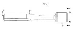
- FIGS. 1A and 1Bare side and cavity-end views respectively of a radiation detection probe according to an embodiment of the present invention
- FIG. 2is an exploded view of the radiation detection probe of FIGS. 1A and 1B ;
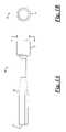
- FIG. 3shows a crystal interconnect according to an embodiment of the present invention
- FIGS. 4A and 4Bare section and end views respectively showing details of a housing according to an embodiment of the present invention.
- FIGS. 5A and 5Bare side and end views respectively showing details of a contact according to an embodiment of the present invention.
- FIG. 6is a partial view in section of a housing showing the arrangement of a stacked crystal array inserted therein according to an embodiment of the present invention.
- FIG. 7is an electrical schematic diagram of the stacked crystal array of FIG. 6 .
- Probe 10comprises a handle 12 , a printed wiring assembly 14 , a connector 16 , a union 17 , a detector interface 18 , a plurality of crystal slices 20 , a pair of crystal interconnects 22 , a pair of insulators 24 , a housing 26 , a contact 28 , a shield 30 and a cap 32 .
- Detector crystal slices 20are generally cylindrical in shape with opposing, generally planar ends. Crystal slices 20 are preferably made of cadmium zinc tellurium (CZT), although any other semiconductor material suitable for detecting photon radiation may be used.
- CZTcadmium zinc tellurium
- Crystal interconnect 22comprises three annular, generally planar, spaced-apart elements or “rings” 34 a, 34 b and 34 c that are oriented generally parallel to each other.
- a first spacer 36 aextends generally orthogonally between rings 34 a and 34 b, maintaining the orientation of these rings.
- a second spacer 36 bextends generally orthogonally between rings 34 b and 34 c, maintaining the orientation of these rings.
- spacers 36 a, 36 bare rotationally offset at an angle ⁇ 1 of about 90 degrees with respect to each other, as shown in FIG. 3 .
- Rings 34 a, 34 b and 34 c and spacers 36 a, 36 bare all in electrical communication with each other.
- Crystal interconnect 22may be made from any suitable conductive material, such as copper beryllium (CuBe), copper/copper alloy, nickel and stainless steel. Platings and coatings such as gold, nickel, silver and tin may also be applied as appropriate and desired.
- CuBecopper beryllium
- Platings and coatingssuch as gold, nickel, silver and tin may also be applied as appropriate and desired.
- the foregoing list of materialsis provided for example purposes only and is not to be considered limiting in any way.
- Insulators 24are generally disc-shaped and have a predetermined thickness with opposing, generally planar sides. Insulators 24 may be made form any suitable electrically insulative material such as, for example, plastics such as TEFLON® (PTFE) (a registered trademark of E. I. du Pont de Nemours and Company), ethylene tetrafluoroethylene (ETFE), polyvinyl chloride (PVC), polyethylene (PE) and crosslinked polyethylene.
- PTFETEFLON®
- ETFEethylene tetrafluoroethylene
- PVCpolyvinyl chloride
- PEpolyethylene
- crosslinked polyethylenecrosslinked polyethylene
- housing 26is generally cylindrical in shape with a cavity 38 disposed therein. Housing 26 also includes a set of elongated slots 40 extending at least partially therethrough. In one embodiment of the present invention slots 40 (shown extending the entire length of the cavity 38 in this embodiment) are oriented at an angle ⁇ 2 of about 90 degrees with respect to each other, as shown in FIG. 4B .
- Housing 26may be made form any suitable electrically insulative material such as, for example, plastics such as TEFLON (PTFE), ethylene tetrafluoroethylene (ETFE), polyvinyl chloride (PVC), polyethylene (PE) and crosslinked polyethylene.
- PTFETEFLON
- ETFEethylene tetrafluoroethylene
- PVCpolyvinyl chloride
- PEpolyethylene
- Contact 28includes a generally planar contact face portion 42 and a stem portion 44 .
- Contact 28may be made from any suitable conductive material, such as copper beryllium (CuBe), copper/copper alloy, nickel and stainless steel. Platings and coatings such as gold, nickel, silver and tin may also be applied as appropriate and desired.
- CuBecopper beryllium
- Platings and coatingssuch as gold, nickel, silver and tin may also be applied as appropriate and desired.
- the foregoing list of materialsis provided for example purposes only and is not to be considered limiting in any way.
- a crystal detector array 46is assembled by installing a contact 28 into housing 26 as shown.
- a pair of crystal interconnects 22are arranged in a series columnar fashion.
- Three crystal slices 20(labeled X 1 , X 2 and X 3 ) and two insulators 24 are placed between the rings of the pair of crystal interconnects 22 in the manner shown.
- This assemblyis then installed into housing 26 such that spacers 36 a, 36 b of a first interconnect 22 fit into a pair of slots 40 of the housing and the spacers of the second interconnect fit into the remaining pair of slots of the housing.
- Crystal detector array 46is shown schematically in FIG. 7 .
- crystal slices 20(labeled X 1 , X 2 and X 3 ) form a parallel electrical circuit.
- the resultant crystal detector array 46yields a photon detector with photon absorption comparable to a monolithic crystal having a thickness generally equivalent to the sum of the thicknesses of the crystal slices. Since the crystal detector array 46 is made from relatively thin crystal slices 20 the probability of defects in the crystal slices is lower. Thus, a higher production yield can be achieved in comparison to a monolithic crystal of the same total thickness, making the array less expensive than the monolithic crystal.
- the required bias voltage for detector array 46is dependent upon the thickness of the individual crystal slices rather than the sum of their thicknesses. This bias voltage is less than that required for a monolithic crystal having a thickness equivalent to the sum of the thicknesses of the individual crystal slices 20 .
- the crystal detector array 46is preferably electrically biased to a voltage corresponding to a ratio of the thickness of the individual crystal slices 20 to that of a monolithic crystal having a thickness generally equivalent to the sum of the thicknesses of the crystal slices.
- the stacked crystal detector array 46 described hereincomprises three crystal slices 20 , two crystal interconnects 22 and two insulators 24 as an example embodiment. However, it is understood that a proportionally greater or lesser number of these components is anticipated within the scope of the invention for various configurations of the array. For example, an array 46 may comprise more than three detector crystal slices 20 with an appropriate number of crystal interconnects 22 and insulators 24 to configure the detector crystal slices into a parallel electrical circuit.
- the crystal interconnect 22 described hereincomprises a set of elements 34 a, 34 b, 34 c shaped as rings with open centers, which is believed to distribute any mechanical shock forces around the circumference of the crystal slices 20 .
- elements 34 a, 34 b and 34 cmay have other shapes within the scope of the invention including, without limitation, annular shapes lacking open centers and any other suitable geometric shape such as, for example, square, rectangular and pentagonal and octagonal shapes with or without open centers.
Landscapes
- Health & Medical Sciences (AREA)
- Physics & Mathematics (AREA)
- Engineering & Computer Science (AREA)
- General Health & Medical Sciences (AREA)
- Nuclear Medicine, Radiotherapy & Molecular Imaging (AREA)
- General Physics & Mathematics (AREA)
- Biomedical Technology (AREA)
- High Energy & Nuclear Physics (AREA)
- Life Sciences & Earth Sciences (AREA)
- Spectroscopy & Molecular Physics (AREA)
- Molecular Biology (AREA)
- Medical Informatics (AREA)
- Optics & Photonics (AREA)
- Radiology & Medical Imaging (AREA)
- Theoretical Computer Science (AREA)
- Pulmonology (AREA)
- Measurement Of Radiation (AREA)
- Condensed Matter Physics & Semiconductors (AREA)
- Chemical & Material Sciences (AREA)
- Crystallography & Structural Chemistry (AREA)
- Pathology (AREA)
- Animal Behavior & Ethology (AREA)
- Public Health (AREA)
- Veterinary Medicine (AREA)
Abstract
Description
- The present invention relates generally to nuclear detection instrumentation, particularly to use of a stacked crystal array in the intra-operative detection of gamma or other X-ray emissions or as an adjunct to positron emission tomography (PET).
- Procedures for the treatment of cancer generally have been based upon the natural history of tumor spread, and thence, upon operative surgical and non-surgical options available to the physician. Surgical operative options generally have looked to the pre-, peri-, intro- and post-surgical physical identification and surgical reduction of tumors, but more recently also to the staging of the cancer's progression through the identification and evaluation of tissue to which the cancer may spread. A variety of techniques have been brought to bear in the art with the purpose of aiding the surgeon in detecting and localizing neoplastic tissue as part of these surgical procedures. (“Neoplastic tissue,” for the present purposes, often is referred to as cancerous tissue, though malignant tumors and malignant tumor cells also are found in the terminology of the art. The term “neoplastic tissue” includes all of these.) Typically, large tumors are readily located by the surgeon by visualization prior to surgery (via imaging mechanisms) and at the operating theater, and, in particular, through palpation, i.e., the feel of tumor as opposed to that of normal tissue. To increase operative success, however, it is necessary for the surgeon to locate “occult” tumors, i.e., tumors which cannot be found by preoperative imaging or the conventional surgical procedures of sight and feel. Failure to locate and remove such occult tumors generally will result in the continued growth of cancer in the patient, a condition often referred to as “recurrent” cancer.
- It is generally also thought that the spread of certain types of solid tumor cancers is caused by the migration (or draining) of tumor cells from the initial tumor to nearby lymph nodes and eventually to other vital sites via the lymphatic system. Cancer surgeons and medical oncologists believe the determination of whether a patient's primary tumor has spread to the lymph nodes is a major determinant of a patient's long-term prognosis. The spread of cancer to the patient's lymph nodes is established by the examination of the nodes by pathology to determine if tumor cells are present. If tumor cells are determined to be present in the lymph nodes, the patient's stage or severity of disease is increased. Surgeons perform procedures to identify the draining node(s) through the injection of a radioactive tracing agent at the site of the primary tumor. Following injection, the tracing agent follows the drainage path of the tumor to the nearest lymph node or nodes, referred to as the “sentinel node(s).” A gamma detection device is used to detect the path of the tracing agent. Since the lymph nodes are connected, oncologists believe that if the sentinel nodes show no sign of malignancy, then the downstream nodes in the pathway are likely to be clear of disease. As such, the removal of other nearby lymph nodes would be clinically unnecessary. Therefore, the ability to rapidly locate and biopsy sentinel nodes provides vital information to the physician in determining if the cancer has spread or if it is localized to the site of the primary tumor.
- Recent technologies now allow the surgeon, via a combination of both isotopically labeled drugs and hand-held radiation detection devices, to provide enhanced surgical evaluation of tumor dissemination, e.g., removal of primary tumor-associated lymph nodes. Such surgical radiation detection instrumentation is comprised generally of a hand-held probe which is in electrical communication with a control console via a flexible cable or, more recently, via wireless communication. This control console is located within the operating room facility but out of the sterile field, while the hand-held probe and forward portions of its associated cable are located within that field. The hand-held radiation detecting probe is relatively small and performs in conjunction with a semiconductor detector such as cadmium zinc tellurium or a scintillating material such as or cesium iodide. Example instrumentation may be found in U.S. Pat. No. 4,782,840, the disclosure of which is expressly incorporated herein by reference.
- Radioactive sources have previously been detected directly at whatever energy levels the source of radiation is producing by using detectors comprised of semiconductor (e.g., cadmium-zinc-tellurium) or scintillating (e.g., cesium iodide) materials. An output signal is produced when an incoming photon collides with material within the detector. The higher the energy level of the primary source of radiation, the more incoming photons can pass completely through the detector without colliding with any material, thus producing no output from the detector. For this reason, high energy detectors have necessarily been made of relatively “thick” (i.e., large cross-section volume) and dense materials to assure that a sufficient number of collisions occur to provide usable detector sensitivity. This characteristic of the detector is often referred to as “stopping power” or “absorption efficiency.”
- In order to more efficiently detect high-energy radiation it is usually necessary to increase the detector absorption by increasing the thickness of the detector crystal. However, thick crystals have a number of disadvantages. Firstly, the probability of defects being present in the crystal volume increases significantly with its thickness. As a result, the yield of such detector crystals is very low, making them relatively expensive to produce. In addition, the efficiency of charge collection in a detector crystal is proportional to the bias voltage applied to a detector of a given thickness. Consequently, if the thickness of the detector is increased by a given amount to increase the absorption probability, the bias voltage applied to the crystal must likewise be increased in order to maintain the same charge collection efficiency. The result is a relatively high operating voltage, which is more difficult to generate and manage, and which may present a safety hazard during use in surgery. There is a need for a cost-effective way to produce a detector crystal assembly having the absorption efficiency of a relatively thick monolithic crystal and which may be biased with a relatively low voltage.
- A stacked crystal array for detecting photon emissions is disclosed according to an embodiment of the present invention. A plurality of relatively thin crystal slices are arranged in a columnar fashion and are electrically connected in parallel. The resultant crystal array yields a photon detector with performance comparable to a monolithic crystal having a similar total crystal thickness. Since the detector is made from a plurality of relatively thin crystal slices a higher production yield can be achieved in comparison to a monolithic crystal having the same total thickness. In addition, the required bias voltage, which is dependent upon the thickness of the individual crystal slices rather than the sum of their thicknesses, is less than that required for a monolithic crystal having the same total thickness.
- In one example embodiment of the present invention a stacked crystal array includes a plurality of crystal slices and a plurality of interconnects. The interconnects have electrically conductive, spaced-apart and generally parallel elements joined by electrically conductive spacers extending generally orthogonally therebetween, the spacers being rotationally offset from each other by a predetermined angle. The array further includes a plurality of electrical insulators and an electrically insulative housing having a plurality of slots. The crystal slices, insulators and interconnects are arranged to form an assembly wherein the crystal slices are coupled together in a parallel electrical circuit, the assembly being inserted into the housing with each of the spacers being located in corresponding slots of the housing. The assembly provides photon absorption comparable to a monolithic crystal having a thickness generally equivalent to the sum of the thicknesses of the crystal slices. In addition, the assembly is electrically biased to a voltage corresponding to a ratio of the thickness of the individual crystal slices to that of a monolithic crystal having a thickness generally equivalent to the sum of the thicknesses of the crystal slices.
- In another example embodiment of the present invention a method for stacking crystal slices comprises the steps of providing a plurality of crystal slices and providing a plurality of interconnects having electrically conductive, spaced-apart and generally parallel elements joined by electrically conductive spacers extending generally orthogonally therebetween, the spacers being rotationally offset from each other by a predetermined angle. Additional steps include providing a plurality of electrical insulators and providing an electrically insulative housing having a plurality of slots. The crystal slices, insulators and interconnects are then assembled to couple the crystal slices together in a parallel electrical circuit. The finished assembly is inserted into the housing such that each of the spacers are located in corresponding slots of the housing. The assembly provides photon absorption comparable to a monolithic crystal having a thickness generally equivalent to the sum of the thicknesses of the crystal slices. In addition, the assembly is electrically biased to a voltage corresponding to a ratio of the thickness of the individual crystal slices to that of a monolithic crystal having a thickness generally equivalent to the sum of the thicknesses of the crystal slices.
- Further features of the inventive embodiments will become apparent to those skilled in the art to which the embodiments relate from reading the specification and claims with reference to the accompanying drawings, in which:
FIGS. 1A and 1B are side and cavity-end views respectively of a radiation detection probe according to an embodiment of the present invention;FIG. 2 is an exploded view of the radiation detection probe ofFIGS. 1A and 1B ;FIG. 3 shows a crystal interconnect according to an embodiment of the present invention;FIGS. 4A and 4B are section and end views respectively showing details of a housing according to an embodiment of the present invention;FIGS. 5A and 5B are side and end views respectively showing details of a contact according to an embodiment of the present invention;FIG. 6 is a partial view in section of a housing showing the arrangement of a stacked crystal array inserted therein according to an embodiment of the present invention; andFIG. 7 is an electrical schematic diagram of the stacked crystal array ofFIG. 6 .- The general arrangement of a
radiation detection probe 10 is shown inFIGS. 1A ,1B and2 according to an embodiment of the present invention.Probe 10 comprises ahandle 12, a printedwiring assembly 14, aconnector 16, aunion 17, adetector interface 18, a plurality of crystal slices20, a pair of crystal interconnects22, a pair ofinsulators 24, ahousing 26, acontact 28, ashield 30 and acap 32. - Detector crystal slices20 are generally cylindrical in shape with opposing, generally planar ends. Crystal slices20 are preferably made of cadmium zinc tellurium (CZT), although any other semiconductor material suitable for detecting photon radiation may be used.
- Details of
crystal interconnect 22 are shown inFIG. 3 .Crystal interconnect 22 comprises three annular, generally planar, spaced-apart elements or “rings”34a,34band34cthat are oriented generally parallel to each other. Afirst spacer 36aextends generally orthogonally betweenrings second spacer 36bextends generally orthogonally betweenrings present invention spacers FIG. 3 .Rings spacers Crystal interconnect 22 may be made from any suitable conductive material, such as copper beryllium (CuBe), copper/copper alloy, nickel and stainless steel. Platings and coatings such as gold, nickel, silver and tin may also be applied as appropriate and desired. The foregoing list of materials is provided for example purposes only and is not to be considered limiting in any way.- Insulators24 (
FIG. 2 ) are generally disc-shaped and have a predetermined thickness with opposing, generally planar sides.Insulators 24 may be made form any suitable electrically insulative material such as, for example, plastics such as TEFLON® (PTFE) (a registered trademark of E. I. du Pont de Nemours and Company), ethylene tetrafluoroethylene (ETFE), polyvinyl chloride (PVC), polyethylene (PE) and crosslinked polyethylene. The foregoing list of materials is provided for example purposes only and is not to be considered limiting in any way. - Details of
housing 26 are shown inFIGS. 4A and 4B .Housing 26 is generally cylindrical in shape with acavity 38 disposed therein.Housing 26 also includes a set ofelongated slots 40 extending at least partially therethrough. In one embodiment of the present invention slots40 (shown extending the entire length of thecavity 38 in this embodiment) are oriented at an angle θ2of about 90 degrees with respect to each other, as shown inFIG. 4B .Housing 26 may be made form any suitable electrically insulative material such as, for example, plastics such as TEFLON (PTFE), ethylene tetrafluoroethylene (ETFE), polyvinyl chloride (PVC), polyethylene (PE) and crosslinked polyethylene. The foregoing list of materials is provided for example purposes only and is not to be considered limiting in any way. - Details of
contact 28 are shown inFIGS. 5A and 5B .Contact 28 includes a generally planarcontact face portion 42 and astem portion 44.Contact 28 may be made from any suitable conductive material, such as copper beryllium (CuBe), copper/copper alloy, nickel and stainless steel. Platings and coatings such as gold, nickel, silver and tin may also be applied as appropriate and desired. The foregoing list of materials is provided for example purposes only and is not to be considered limiting in any way. - With reference now to
FIG. 6 , acrystal detector array 46 is assembled by installing acontact 28 intohousing 26 as shown. A pair of crystal interconnects22 are arranged in a series columnar fashion. Three crystal slices20 (labeled X1, X2 and X3) and twoinsulators 24 are placed between the rings of the pair of crystal interconnects22 in the manner shown. This assembly is then installed intohousing 26 such thatspacers first interconnect 22 fit into a pair ofslots 40 of the housing and the spacers of the second interconnect fit into the remaining pair of slots of the housing. - In operation, a bias voltage having a polarity shown in
FIG. 6 is applied tocrystal detector array 46 in any convenient manner viacontact 28 marked “(+)” and the exposedring 34cofdetector array 46 marked “(−)”.Crystal detector array 46 is shown schematically inFIG. 7 . As can be seen, crystal slices20 (labeled X1, X2 and X3) form a parallel electrical circuit. The resultantcrystal detector array 46 yields a photon detector with photon absorption comparable to a monolithic crystal having a thickness generally equivalent to the sum of the thicknesses of the crystal slices. Since thecrystal detector array 46 is made from relatively thin crystal slices20 the probability of defects in the crystal slices is lower. Thus, a higher production yield can be achieved in comparison to a monolithic crystal of the same total thickness, making the array less expensive than the monolithic crystal. - Because of the parallel-circuit arrangement of crystal slices20 the required bias voltage for
detector array 46 is dependent upon the thickness of the individual crystal slices rather than the sum of their thicknesses. This bias voltage is less than that required for a monolithic crystal having a thickness equivalent to the sum of the thicknesses of the individual crystal slices20. Stated another way, thecrystal detector array 46 is preferably electrically biased to a voltage corresponding to a ratio of the thickness of the individual crystal slices20 to that of a monolithic crystal having a thickness generally equivalent to the sum of the thicknesses of the crystal slices. - The stacked
crystal detector array 46 described herein comprises threecrystal slices 20, twocrystal interconnects 22 and twoinsulators 24 as an example embodiment. However, it is understood that a proportionally greater or lesser number of these components is anticipated within the scope of the invention for various configurations of the array. For example, anarray 46 may comprise more than three detector crystal slices20 with an appropriate number of crystal interconnects22 andinsulators 24 to configure the detector crystal slices into a parallel electrical circuit. - The
crystal interconnect 22 described herein comprises a set ofelements elements - While this invention has been shown and described with respect to a detailed embodiment thereof, it will be understood by those skilled in the art that changes in form and detail thereof may be made without departing from the scope of the claims of the invention.
Claims (20)
Priority Applications (8)
| Application Number | Priority Date | Filing Date | Title |
|---|---|---|---|
| PCT/US2009/043882WO2010132056A1 (en) | 2009-05-14 | 2009-05-14 | Stacked crystal array for detection of photon emissions |
| CA2761544ACA2761544A1 (en) | 2009-05-14 | 2009-05-14 | Stacked crystal array for detection of photon emissions |
| CN200980159656.5ACN102460214B (en) | 2009-05-14 | 2009-05-14 | Stacked crystal arrays for photon emission detection |
| CN201410126165.3ACN103995276B (en) | 2009-05-14 | 2009-05-14 | Probe for detecting radiation |
| EP09844736AEP2430475A1 (en) | 2009-05-14 | 2009-05-14 | Stacked crystal array for detection of photon emissions |
| US12/465,672US8269185B2 (en) | 2009-05-14 | 2009-05-14 | Stacked crystal array for detection of photon emissions |
| KR1020117030003AKR101690059B1 (en) | 2009-05-14 | 2009-05-14 | Stacked crystal array for detection of photon emissions |
| US13/589,278US9500750B2 (en) | 2009-05-14 | 2012-08-20 | Stacked crystal array for detection of photon emissions |
Applications Claiming Priority (1)
| Application Number | Priority Date | Filing Date | Title |
|---|---|---|---|
| US12/465,672US8269185B2 (en) | 2009-05-14 | 2009-05-14 | Stacked crystal array for detection of photon emissions |
Related Child Applications (1)
| Application Number | Title | Priority Date | Filing Date |
|---|---|---|---|
| US13/589,278ContinuationUS9500750B2 (en) | 2009-05-14 | 2012-08-20 | Stacked crystal array for detection of photon emissions |
Publications (2)
| Publication Number | Publication Date |
|---|---|
| US20100288936A1true US20100288936A1 (en) | 2010-11-18 |
| US8269185B2 US8269185B2 (en) | 2012-09-18 |
Family
ID=43067755
Family Applications (2)
| Application Number | Title | Priority Date | Filing Date |
|---|---|---|---|
| US12/465,672Active2030-11-22US8269185B2 (en) | 2009-05-14 | 2009-05-14 | Stacked crystal array for detection of photon emissions |
| US13/589,278Active2031-08-23US9500750B2 (en) | 2009-05-14 | 2012-08-20 | Stacked crystal array for detection of photon emissions |
Family Applications After (1)
| Application Number | Title | Priority Date | Filing Date |
|---|---|---|---|
| US13/589,278Active2031-08-23US9500750B2 (en) | 2009-05-14 | 2012-08-20 | Stacked crystal array for detection of photon emissions |
Country Status (6)
| Country | Link |
|---|---|
| US (2) | US8269185B2 (en) |
| EP (1) | EP2430475A1 (en) |
| KR (1) | KR101690059B1 (en) |
| CN (2) | CN102460214B (en) |
| CA (1) | CA2761544A1 (en) |
| WO (1) | WO2010132056A1 (en) |
Cited By (4)
| Publication number | Priority date | Publication date | Assignee | Title |
|---|---|---|---|---|
| US9012854B2 (en) | 2011-05-12 | 2015-04-21 | Koninklijke Philips N.V. | Optimized scintilator crystals for PET |
| WO2017075080A1 (en)* | 2015-10-27 | 2017-05-04 | Devicor Medical Products, Inc. | Surgical probe apparatus and system and method of use thereof |
| US20210219928A1 (en)* | 2020-01-17 | 2021-07-22 | Actis IP Holdings, LLC | Electronic collimation and depth detection in a side-viewing laparoscopic probe for the detection of high energy gamma radiation |
| US11956048B2 (en) | 2018-09-28 | 2024-04-09 | Apple Inc. | Systems and methods for measurement period and accuracy for beam reporting based on L1-RSRP |
Families Citing this family (1)
| Publication number | Priority date | Publication date | Assignee | Title |
|---|---|---|---|---|
| US11191498B2 (en) | 2015-10-27 | 2021-12-07 | Devicor Medical Products, Inc. | Surgical probe and apparatus with improved graphical display |
Citations (16)
| Publication number | Priority date | Publication date | Assignee | Title |
|---|---|---|---|---|
| US3142756A (en)* | 1959-11-23 | 1964-07-28 | Schlumberger Well Surv Corp | Photomultiplier tube with tubular cathode bonded to the interior surface thereof |
| US4230510A (en)* | 1977-11-21 | 1980-10-28 | General Electric Company | Distributed phosphor scintillator structures |
| US4292538A (en)* | 1979-08-08 | 1981-09-29 | Technicare Corporation | Shaped detector |
| US4782840A (en)* | 1984-03-02 | 1988-11-08 | Neoprobe Corporation | Method for locating, differentiating, and removing neoplasms |
| US4801803A (en)* | 1987-03-17 | 1989-01-31 | Neoprobe Corporation | Detector and localizer for low energy radiation emissions |
| US5068524A (en)* | 1988-12-05 | 1991-11-26 | The Secretary Of State For Defence In Her Britannic Majesty's Government Of The United Kingdom Of Great Britain And Northern Ireland | Multiple heterostructure photodetector |
| US5091650A (en)* | 1989-12-15 | 1992-02-25 | Hamamatsu Photonics K. K. | Radiation detector using scintillator array |
| US5227633A (en)* | 1991-03-20 | 1993-07-13 | Shin-Etsu Chemical Co., Ltd. | Joined scintillator block body for radiation detector |
| US5616925A (en)* | 1995-06-07 | 1997-04-01 | Santa Barbara Research Center | Gamma ray detector with improved resolution and method of fabrication |
| US5907156A (en)* | 1995-03-22 | 1999-05-25 | Mitsubishi Denki Kabushiki Kaisha | Wide range radiation detector |
| US6236051B1 (en)* | 1998-03-27 | 2001-05-22 | Kabushiki Kaisha Toshiba | Semiconductor radiation detector |
| US6452184B1 (en)* | 1997-11-28 | 2002-09-17 | Nanocrystal Imaging Corp. | Microchannel high resolution x-ray sensor having an integrated photomultiplier |
| US6563120B1 (en)* | 2002-03-06 | 2003-05-13 | Ronan Engineering Co. | Flexible radiation detector scintillator |
| US20050067577A1 (en)* | 2003-09-30 | 2005-03-31 | Norihito Yanagita | Semiconductor radiation detector and radiological imaging apparatus |
| US20050230628A1 (en)* | 2002-08-21 | 2005-10-20 | Tadaaki Hirai | Radiation detector |
| US20050253073A1 (en)* | 2002-07-17 | 2005-11-17 | Christian Joram | Gamma ray detector for positron emission tomography (pet) and single photon emisson computed tomography (spect) |
Family Cites Families (22)
| Publication number | Priority date | Publication date | Assignee | Title |
|---|---|---|---|---|
| US3691389A (en) | 1969-06-09 | 1972-09-12 | Ronald Ellis | Radiation detector comprising semi-conductor body incorporating a two-dimensional array of p-i-n-devices |
| US6046454A (en) | 1995-10-13 | 2000-04-04 | Digirad Corporation | Semiconductor radiation detector with enhanced charge collection |
| GB2307785B (en) | 1995-11-29 | 1998-04-29 | Simage Oy | Forming contacts on semiconductor substrates for radiation detectors and imaging devices |
| US6175120B1 (en) | 1998-05-08 | 2001-01-16 | The Regents Of The University Of Michigan | High-resolution ionization detector and array of such detectors |
| DE69835240T2 (en) | 1998-09-24 | 2007-06-06 | Elgems Ltd. | PHOTON DETECTOR IN THE FORM OF A PIXEL MATRIX |
| FR2792418B1 (en) | 1999-04-15 | 2001-06-01 | Commissariat Energie Atomique | TWO-DIMENSIONAL DETECTOR OF IONIZING RADIATION AND METHOD OF MANUFACTURING THE SAME |
| US6480562B2 (en) | 2000-12-05 | 2002-11-12 | Ge Medical Systems Global Technology Company, Llc | Apparatus and method of converting electromagnetic energy directly to electrons for computed tomography imaging |
| IL143980A0 (en) | 2001-06-25 | 2002-04-21 | Imarad Imaging Systems Ltd | Three dimensional radiation detection |
| US6781132B2 (en) | 2001-08-10 | 2004-08-24 | The Regents Of The University Of Michigan | Collimated radiation detector assembly, array of collimated radiation detectors and collimated radiation detector module |
| US6979215B2 (en)* | 2001-11-28 | 2005-12-27 | Molex Incorporated | High-density connector assembly with flexural capabilities |
| US20030178570A1 (en)* | 2002-03-25 | 2003-09-25 | Hitachi Metals, Ltd. | Radiation detector, manufacturing method thereof and radiation CT device |
| KR100455901B1 (en)* | 2002-03-26 | 2004-11-06 | 한국몰렉스 주식회사 | High speed communication cable connector assembly with stacking structure |
| JP2003344548A (en) | 2002-05-24 | 2003-12-03 | Seiko Instruments Inc | Radiation detector |
| FI20021255A7 (en) | 2002-06-27 | 2003-12-28 | Metorex Int Oy | Direct conversion imaging X-ray detector and imaging arrangement using the same |
| US20040061058A1 (en) | 2002-09-30 | 2004-04-01 | Williams James Richard | Scintillation detector with gadolinium based sidewall axial restraint and compliance assembly |
| US6887441B2 (en)* | 2002-09-30 | 2005-05-03 | The Regents Of The University Of California | High resistivity aluminum antimonide radiation detector |
| US7119340B2 (en) | 2002-10-07 | 2006-10-10 | Hitachi, Ltd. | Radiation detector, radiation detector element, and radiation imaging apparatus |
| US8586932B2 (en) | 2004-11-09 | 2013-11-19 | Spectrum Dynamics Llc | System and method for radioactive emission measurement |
| US6953935B1 (en) | 2004-05-11 | 2005-10-11 | General Electric Company | CT detector fabrication process |
| US20060033029A1 (en) | 2004-08-13 | 2006-02-16 | V-Target Technologies Ltd. | Low-voltage, solid-state, ionizing-radiation detector |
| US7252696B2 (en)* | 2004-09-02 | 2007-08-07 | Carrier Corporation | Fan coil media cabinet |
| US7439518B2 (en) | 2006-04-07 | 2008-10-21 | Raytheon Company | Multi-layer pixellated gamma-ray detector |
- 2009
- 2009-05-14WOPCT/US2009/043882patent/WO2010132056A1/enactiveApplication Filing
- 2009-05-14CACA2761544Apatent/CA2761544A1/ennot_activeAbandoned
- 2009-05-14USUS12/465,672patent/US8269185B2/enactiveActive
- 2009-05-14EPEP09844736Apatent/EP2430475A1/ennot_activeWithdrawn
- 2009-05-14CNCN200980159656.5Apatent/CN102460214B/ennot_activeExpired - Fee Related
- 2009-05-14KRKR1020117030003Apatent/KR101690059B1/enactiveActive
- 2009-05-14CNCN201410126165.3Apatent/CN103995276B/enactiveActive
- 2012
- 2012-08-20USUS13/589,278patent/US9500750B2/enactiveActive
Patent Citations (16)
| Publication number | Priority date | Publication date | Assignee | Title |
|---|---|---|---|---|
| US3142756A (en)* | 1959-11-23 | 1964-07-28 | Schlumberger Well Surv Corp | Photomultiplier tube with tubular cathode bonded to the interior surface thereof |
| US4230510A (en)* | 1977-11-21 | 1980-10-28 | General Electric Company | Distributed phosphor scintillator structures |
| US4292538A (en)* | 1979-08-08 | 1981-09-29 | Technicare Corporation | Shaped detector |
| US4782840A (en)* | 1984-03-02 | 1988-11-08 | Neoprobe Corporation | Method for locating, differentiating, and removing neoplasms |
| US4801803A (en)* | 1987-03-17 | 1989-01-31 | Neoprobe Corporation | Detector and localizer for low energy radiation emissions |
| US5068524A (en)* | 1988-12-05 | 1991-11-26 | The Secretary Of State For Defence In Her Britannic Majesty's Government Of The United Kingdom Of Great Britain And Northern Ireland | Multiple heterostructure photodetector |
| US5091650A (en)* | 1989-12-15 | 1992-02-25 | Hamamatsu Photonics K. K. | Radiation detector using scintillator array |
| US5227633A (en)* | 1991-03-20 | 1993-07-13 | Shin-Etsu Chemical Co., Ltd. | Joined scintillator block body for radiation detector |
| US5907156A (en)* | 1995-03-22 | 1999-05-25 | Mitsubishi Denki Kabushiki Kaisha | Wide range radiation detector |
| US5616925A (en)* | 1995-06-07 | 1997-04-01 | Santa Barbara Research Center | Gamma ray detector with improved resolution and method of fabrication |
| US6452184B1 (en)* | 1997-11-28 | 2002-09-17 | Nanocrystal Imaging Corp. | Microchannel high resolution x-ray sensor having an integrated photomultiplier |
| US6236051B1 (en)* | 1998-03-27 | 2001-05-22 | Kabushiki Kaisha Toshiba | Semiconductor radiation detector |
| US6563120B1 (en)* | 2002-03-06 | 2003-05-13 | Ronan Engineering Co. | Flexible radiation detector scintillator |
| US20050253073A1 (en)* | 2002-07-17 | 2005-11-17 | Christian Joram | Gamma ray detector for positron emission tomography (pet) and single photon emisson computed tomography (spect) |
| US20050230628A1 (en)* | 2002-08-21 | 2005-10-20 | Tadaaki Hirai | Radiation detector |
| US20050067577A1 (en)* | 2003-09-30 | 2005-03-31 | Norihito Yanagita | Semiconductor radiation detector and radiological imaging apparatus |
Cited By (9)
| Publication number | Priority date | Publication date | Assignee | Title |
|---|---|---|---|---|
| US9012854B2 (en) | 2011-05-12 | 2015-04-21 | Koninklijke Philips N.V. | Optimized scintilator crystals for PET |
| WO2017075080A1 (en)* | 2015-10-27 | 2017-05-04 | Devicor Medical Products, Inc. | Surgical probe apparatus and system and method of use thereof |
| KR20180074704A (en)* | 2015-10-27 | 2018-07-03 | 데비코어 메디컬 프로덕츠, 인코포레이티드 | SURGICAL PROBE DEVICE AND SYSTEM AND METHOD OF USING THE SAME |
| JP2019501371A (en)* | 2015-10-27 | 2019-01-17 | デビコー・メディカル・プロダクツ・インコーポレイテッドDevicor Medical Products, Inc. | Surgical probe device, and system and method using the same |
| EP3871605A1 (en)* | 2015-10-27 | 2021-09-01 | Devicor Medical Products, Inc. | Surgical probe apparatus and system |
| KR102428056B1 (en) | 2015-10-27 | 2022-08-03 | 데비코어 메디컬 프로덕츠, 인코포레이티드 | Surgical probe device and system and method of use thereof |
| US11956048B2 (en) | 2018-09-28 | 2024-04-09 | Apple Inc. | Systems and methods for measurement period and accuracy for beam reporting based on L1-RSRP |
| US20210219928A1 (en)* | 2020-01-17 | 2021-07-22 | Actis IP Holdings, LLC | Electronic collimation and depth detection in a side-viewing laparoscopic probe for the detection of high energy gamma radiation |
| US12213822B2 (en)* | 2020-01-17 | 2025-02-04 | Actis IP Holdings, LLC | Electronic collimation and depth detection in a side-viewing laparoscopic probe for the detection of high energy gamma radiation |
Also Published As
| Publication number | Publication date |
|---|---|
| US20120318995A1 (en) | 2012-12-20 |
| US8269185B2 (en) | 2012-09-18 |
| CN103995276B (en) | 2017-09-22 |
| WO2010132056A1 (en) | 2010-11-18 |
| CN103995276A (en) | 2014-08-20 |
| CN102460214B (en) | 2014-05-07 |
| KR101690059B1 (en) | 2016-12-27 |
| US9500750B2 (en) | 2016-11-22 |
| CN102460214A (en) | 2012-05-16 |
| CA2761544A1 (en) | 2010-11-18 |
| EP2430475A1 (en) | 2012-03-21 |
| KR20120030420A (en) | 2012-03-28 |
Similar Documents
| Publication | Publication Date | Title |
|---|---|---|
| US9500750B2 (en) | Stacked crystal array for detection of photon emissions | |
| ES2264683T3 (en) | INTRAVASCULAR IMAGE REPRESENTATION DETECTOR. | |
| US6744051B2 (en) | High density electrical interconnect system for photon emission tomography scanner | |
| WO2010120525A1 (en) | Interwoven multi-aperture collimator for 3-dimensional radiation imaging applications | |
| CN111936051B (en) | Tethered laparoscopic probe | |
| US20110042575A1 (en) | Semiconductor Detector Block and Positron Emission Tomography Device Using the Same | |
| US10228472B2 (en) | Radiation position detection method, radiation position detector, and pet apparatus | |
| US20190079204A1 (en) | Radiation position detection method, radiation position detector, and pet apparatus | |
| JP4352841B2 (en) | Radiation detector and RI imaging apparatus | |
| NL2021303B1 (en) | Active collimator system comprising a monolayer of monolithic converters | |
| US10969502B2 (en) | Positron or beta particle detector | |
| IL268390B2 (en) | Theranostic imaging with czt gamma cameras | |
| WO2008072343A1 (en) | Positron ct apparatus | |
| US9494696B1 (en) | K-alpha probe for detection of photon emissions | |
| US7501635B2 (en) | Tomograph comprising detectors having a specific shape | |
| JP2008116260A (en) | Semiconductor detector block and positron emission tomography apparatus using the same | |
| Farghaly | Diagnostic accuracy of 18F-FDG PET/CT in detection of local recurrence in rectal cancer and the added value of dual time point scanning | |
| Montravers et al. | Detection of recurrent colorectal carcinoma by 18F-FDG: comparison of the clinical performances of FDG PET and FDG CDET | |
| Raylman et al. | Arrays of segmented, tapered light guides for use with large, planar scintillation detectors | |
| JPH03231186A (en) | Positron ct equipment | |
| Myronakis et al. | Integrated PET/SPECT system for breast imaging with CdZnTe: Computational assessment | |
| Li | Design study of a two-panel head-and-neck cancer dedicated position emission tomography system | |
| Hsu | Investigation of Advanced Clinical PET System Designs | |
| Ni et al. | Scatter fraction performance tests for positron imaging system with dual plane geometry | |
| Skehan | Positron Emission Tomography in the Management of Colon Cancer |
Legal Events
| Date | Code | Title | Description |
|---|---|---|---|
| AS | Assignment | Owner name:NEOPROBE CORPORATION, OHIO Free format text:ASSIGNMENT OF ASSIGNORS INTEREST;ASSIGNOR:CALL, JOHN D.;REEL/FRAME:022684/0243 Effective date:20090513 | |
| AS | Assignment | Owner name:DEVICOR MEDICAL PRODUCTS, INC., OHIO Free format text:ASSIGNMENT OF ASSIGNORS INTEREST;ASSIGNOR:NEOPROBE CORPORATION;REEL/FRAME:026862/0873 Effective date:20110817 | |
| AS | Assignment | Owner name:GENERAL ELECTRIC CAPITAL CORPORATION, AS AGENT, MA Free format text:SECURITY AGREEMENT;ASSIGNOR:DEVICOR MEDICAL PRODUCTS, INC.;REEL/FRAME:027021/0180 Effective date:20110817 | |
| STCF | Information on status: patent grant | Free format text:PATENTED CASE | |
| FEPP | Fee payment procedure | Free format text:PAYOR NUMBER ASSIGNED (ORIGINAL EVENT CODE: ASPN); ENTITY STATUS OF PATENT OWNER: LARGE ENTITY | |
| FPAY | Fee payment | Year of fee payment:4 | |
| FEPP | Fee payment procedure | Free format text:PAT HOLDER NO LONGER CLAIMS SMALL ENTITY STATUS, ENTITY STATUS SET TO UNDISCOUNTED (ORIGINAL EVENT CODE: STOL); ENTITY STATUS OF PATENT OWNER: LARGE ENTITY | |
| MAFP | Maintenance fee payment | Free format text:PAYMENT OF MAINTENANCE FEE, 8TH YEAR, LARGE ENTITY (ORIGINAL EVENT CODE: M1552); ENTITY STATUS OF PATENT OWNER: LARGE ENTITY Year of fee payment:8 | |
| MAFP | Maintenance fee payment | Free format text:PAYMENT OF MAINTENANCE FEE, 12TH YEAR, LARGE ENTITY (ORIGINAL EVENT CODE: M1553); ENTITY STATUS OF PATENT OWNER: LARGE ENTITY Year of fee payment:12 |