US20100278955A1 - Imprint Alignment Method, System and Template - Google Patents
Imprint Alignment Method, System and TemplateDownload PDFInfo
- Publication number
- US20100278955A1 US20100278955A1US12/835,181US83518110AUS2010278955A1US 20100278955 A1US20100278955 A1US 20100278955A1US 83518110 AUS83518110 AUS 83518110AUS 2010278955 A1US2010278955 A1US 2010278955A1
- Authority
- US
- United States
- Prior art keywords
- template
- alignment
- layer
- pattern
- alignment marks
- Prior art date
- Legal status (The legal status is an assumption and is not a legal conclusion. Google has not performed a legal analysis and makes no representation as to the accuracy of the status listed.)
- Granted
Links
Images


Classifications
- G—PHYSICS
- G03—PHOTOGRAPHY; CINEMATOGRAPHY; ANALOGOUS TECHNIQUES USING WAVES OTHER THAN OPTICAL WAVES; ELECTROGRAPHY; HOLOGRAPHY
- G03F—PHOTOMECHANICAL PRODUCTION OF TEXTURED OR PATTERNED SURFACES, e.g. FOR PRINTING, FOR PROCESSING OF SEMICONDUCTOR DEVICES; MATERIALS THEREFOR; ORIGINALS THEREFOR; APPARATUS SPECIALLY ADAPTED THEREFOR
- G03F7/00—Photomechanical, e.g. photolithographic, production of textured or patterned surfaces, e.g. printing surfaces; Materials therefor, e.g. comprising photoresists; Apparatus specially adapted therefor
- G03F7/70—Microphotolithographic exposure; Apparatus therefor
- G03F7/70216—Mask projection systems
- G03F7/7035—Proximity or contact printers
- G—PHYSICS
- G03—PHOTOGRAPHY; CINEMATOGRAPHY; ANALOGOUS TECHNIQUES USING WAVES OTHER THAN OPTICAL WAVES; ELECTROGRAPHY; HOLOGRAPHY
- G03F—PHOTOMECHANICAL PRODUCTION OF TEXTURED OR PATTERNED SURFACES, e.g. FOR PRINTING, FOR PROCESSING OF SEMICONDUCTOR DEVICES; MATERIALS THEREFOR; ORIGINALS THEREFOR; APPARATUS SPECIALLY ADAPTED THEREFOR
- G03F7/00—Photomechanical, e.g. photolithographic, production of textured or patterned surfaces, e.g. printing surfaces; Materials therefor, e.g. comprising photoresists; Apparatus specially adapted therefor
- G03F7/70—Microphotolithographic exposure; Apparatus therefor
- G03F7/70483—Information management; Active and passive control; Testing; Wafer monitoring, e.g. pattern monitoring
- G03F7/70605—Workpiece metrology
- G03F7/70616—Monitoring the printed patterns
- G03F7/70633—Overlay, i.e. relative alignment between patterns printed by separate exposures in different layers, or in the same layer in multiple exposures or stitching
- Y—GENERAL TAGGING OF NEW TECHNOLOGICAL DEVELOPMENTS; GENERAL TAGGING OF CROSS-SECTIONAL TECHNOLOGIES SPANNING OVER SEVERAL SECTIONS OF THE IPC; TECHNICAL SUBJECTS COVERED BY FORMER USPC CROSS-REFERENCE ART COLLECTIONS [XRACs] AND DIGESTS
- Y10—TECHNICAL SUBJECTS COVERED BY FORMER USPC
- Y10S—TECHNICAL SUBJECTS COVERED BY FORMER USPC CROSS-REFERENCE ART COLLECTIONS [XRACs] AND DIGESTS
- Y10S977/00—Nanotechnology
- Y10S977/84—Manufacture, treatment, or detection of nanostructure
- Y10S977/887—Nanoimprint lithography, i.e. nanostamp
Definitions
- the present inventionrelates to a method of improving imprint lithography alignment as well as a system and template to be used for same.
- the method, system, and template herein describedhave particular utility in subfield alignment of sub 100 nm features requiring registration of about 25 nm.
- Micro-fabricationinvolves the fabrication of very small structures, e.g., having features on the order of micrometers or smaller.
- One industry that has been driving the fabrication of increasingly smaller structuresis the electronics industry. As electronic devices have become smaller and faster, the integrated circuits that drive them have necessarily become smaller.
- a technique known as ‘photolithography’, or simply ‘lithography’,is typically employed in the manufacture of integrated circuits.
- Lithographic techniquesare generally used to pattern the various levels of an integrated circuit.
- these lithographic techniquesinclude applying a photosensitive material to a semiconductor substrate.
- photosensitive materialscommonly referred to as “resist,” are selectively exposed to a form of radiation.
- An exposure tool and photomaskare often used to obtain the desired selective exposure. Such exposure changes the solubility of the resist such that the photomask's pattern is formed in the resist following a development process to remove the soluble resist.
- the resulting patterned resistserves to protect underlying conductive or dielectric material from etching or ion implantation.
- the photomask patternmust be properly aligned to previously formed semiconductor topography features during the lithography process.
- lithographic misalignmentmay lead to shorting between structures that should be isolated from each other, and isolation of structures that should be coupled to each other.
- Imprint lithographyis capable of manufacturably producing sub-100 nm features.
- Several imprint lithography techniqueshave been investigated as low cost, high volume manufacturing alternatives to conventional photolithography for high-resolution patterning.
- a relief image in a templateis used to replicate a surface relief into a polymerizable material arranged upon the surface of a substrate.
- the templatemakes mechanical contact with the material arranged upon the substrate, and the material is subjected to conditions to solidify and/or to polymerize the same such that a relief structure complimentary to that of the template is formed on the substrate.
- the materialmay be solidified or polymerized by, for example, heat or actinic light.
- Such patterning and polymerization techniquesmay be referred to as thermal imprint lithography or ultraviolet (‘UV’) imprint lithography, respectively.
- Typical substratesmay include semiconductors, dielectric materials, magnetic materials, or optoelectronic materials.
- Imprint lithographymay be used in wide variety of applications. That is, imprint lithography applications are not limited to the manufacture of integrated circuits. However, typical applications require alignment of subsequently imprinted device layers to previously imprinted device layers. Properly aligning subsequent imprint lithography device layers becomes increasingly difficult as feature sizes become ever smaller. Imprint lithography systems are currently capable of printing features in the sub-100 nm range with a 3 ⁇ overlay alignment capability of less than about 500 nm. Despite a high degree of alignment accuracy, current imprint lithography systems are challenged by the degree of precision required to consistently align multiple layers having minimum feature sizes. Devices having such minimum feature sizes may also have registration tolerances of about 25 nm or less. Consequently, proper alignment of multi-layered devices having minimum feature sizes may be a relatively infrequent event. It is desired, therefore, to provide improvement to imprint lithography alignment.
- the method of improving lithographic alignmentessentially comprises imprinting a first layer on a substrate and imprinting a second layer on the first layer, the first layer including an array of first-layer geometries each arranged within a respective subfield with each first-layer geometry including at least one first-layer feature, and the second layer including an array of second-layer geometries each arranged within a respective subfield with each second-layer geometry including at least one second-layer feature, where at least one second-layer feature has at least one corresponding first-layer feature, where at least one second-layer geometry has a corresponding first-layer geometry, and where at least one second-layer geometry is intentionally offset from its corresponding first-layer geometry.
- at least two second-layer geometriesare intentionally offset from their corresponding first layer geometries, and said offsets are not equal.
- the present inventionessentially comprises a method of improving lithographic alignment between subsequent imprinted device layers within a subfield.
- a methodincludes establishing an (x,y) grid whereby a centermost point of a subfield arranged within a central region has (x,y) coordinates (0,0).
- Such a methodfurther includes establishing an array having ‘N’ subfields arranged in ‘J’ rows and ‘K’ columns, where each column has a width ‘w’ and each row has a height ‘h’, and a device is arranged entirely within a single subfield.
- the methodfurther includes imprinting a first layer having an array of ‘N’ first-layer geometries, where a centermost point of a central first-layer geometry has (x,y) coordinates (0,0), where a centermost point of each first-layer geometry is commensurate with a centermost point of its respective subfield, where a centermost point of a first-layer geometry is a spaced distance ‘w’ from a centermost point of an immediately laterally adjacent first-layer geometry, and where a centermost point of a first-layer geometry is a spaced distance ‘h’ from a centermost point of an immediately vertically adjacent first-layer geometry.
- the methodfurther includes imprinting a second layer, where the second layer includes an array of ‘N’ second-layer geometries, where each second-layer geometry has a corresponding first-layer geometry, where a centermost point of a central second-layer geometry has (x,y) coordinates (0,0), where a centermost point of a second-layer geometry is a spaced distance ‘w+ ⁇ w’ from a centermost point of an immediately laterally adjacent second-layer geometry and a centermost point of a second-layer geometry is a spaced distance ‘h+ ⁇ h’ from a centermost point of an immediately vertically adjacent first-layer geometry, where ⁇ w and ⁇ h are both non-zero.
- the present inventionessentially comprises a set of lithography templates providing improved lithographic alignment.
- a template setincludes a first template having an array of first geometries and a second template having an array of second geometries, where each second geometry has a corresponding first geometry, and where at least one second geometry is intentionally offset from its corresponding first geometry.
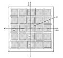
- FIG. 1is a plan view of a wafer substrate illustrating the wafer field and the print fields which comprise the wafer field.
- FIG. 2is a plan view of a print field having multiple subfields.
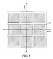
- FIG. 3is a plan view of a print field having first and second-layer geometries imprinted thereupon.
- FIG. 4is a plan view of the print field of FIG. 4 imposed upon x and y axes.
- FIG. 5is a more detailed view of FIG. 5 .
- an imprint lithography systemmay have a high degree of alignment accuracy, the alignment precision may not suffice for multi-layered devices having sub 100 nm features.
- a system having a three sigma alignment accuracy of less than about 500 nmmay not be sufficient to produce functional, multi-layered devices having, for example, registration tolerances of about 25 nm or less, and having minimum feature sizes of, for example, about 50 nm or less.
- An exemplary lithographic systemis available under the trade name IMPRIO® 100 from Molecular Imprints, Inc. having a place of business at 1807 Braker Lane, Bldg. C-100, Austin, Tex. 78758. The system description for the IMPRIO® 100 is available at www.molecularimprints.com and is incorporated herein by reference.
- FIG. 1illustrates substrate 16 , which in this case is a semiconductor wafer.
- a wafer field 18comprising print fields 20 .
- a wafer field 18is comprised of an integral number of print fields 20 .
- the dimensions of a print fieldmay be as large as a lithography system's maximum field.
- An imprint lithography system' maximum fieldis the largest area the system can simultaneously imprint. That is, the maximum area that can be imprinted with one flash.
- the maximum field size of an imprint lithography systemis 25 mm ⁇ 25 mm.
- An optical lithography system's maximum fieldis the largest area the system can expose in one exposure.
- the instant inventionis directed toward an imprint lithography system, the methods, systems, and templates described herein may also be applicable to at least some optical lithography systems.
- FIG. 2illustrates a print field 20 having multiple subfields 22 .
- a print fieldis comprised of an integral number of subfields.
- Subfields 22are shown a spaced distance from the perimeter of the print field 20 merely for clarification.
- the subfields 22are shown a spaced distance from one another merely for clarification.
- subfields 22may abut one another.
- Each subfieldmay accommodate one or more devices. The devices may or may not have similar geometries, features, and/or functions.
- a first-layer geometryis created within each subfield 22 .
- the first layer geometryincludes first-layer features for one or more devices which may or may not be similar.
- the first layer featuresmay have minimum feature sizes in the range of, for example, 100 nm or smaller.
- Each first-layer geometryis arranged such that its features are arranged entirely within its respective subfield 22 .
- the first layer geometryhas a centermost point which is substantially commensurate with the centermost point of the subfield.
- each first-layer geometryis similarly arranged within its corresponding subfield. Such arrangement is in contrast to the second-layer geometries to be discussed below.
- FIG. 3illustrates the print field 20 having second-layer geometries 24 imprinted upon first-layer geometries.
- Each second-layer geometryis comprised of second-layer features, where at least one second-layer feature has a corresponding first-layer feature to which proper alignment is required for proper device operation.
- a second-layer geometrywill occupy the same approximate area as its corresponding first-layer geometry. Therefore, it is noted that first-layer geometries do not necessarily extend to the perimeter of their respective subfields, as second-layer geometries may be printed entirely within their respective subfields.
- first-layer or second-layer geometriesmay not necessarily include sacrificial diagnostic features. Such features may be created within the print field yet outside the subfields.
- each offset second-layer geometryhas a unique offset.
- each offset with respect to a centermost point of the subfieldmay be a multiple of about 25 nm. In this case, the offset multiple is therefore 25 nm.
- the offset multipleis a function of the capability of the lithography template-making process, system, and apparatus(es). Consequently, as template manufacturing improves, offset multiples may shrink accordingly.
- FIG. 4illustrates the arrangement of the first-layer geometries and second-layer geometries with the aid of an (x,y) axis.
- Central second-layer geometry 26is arranged such that its centermost point is substantially commensurate with the origin of the axis, (0,0).
- Each columnhas a width ‘w’ and each row has a height ‘h’.
- the first-layer geometriesare spaced commensurate with the subfields. Thus, the first layer geometries are not offset with respect to their respective subfields.
- a center of any first-layer geometryis a horizontal distance of ‘w’ or a vertical distance of ‘h’ from any immediately laterally adjacent first-layer geometry.
- ‘w’equals ‘h’
- the centers of the first-layer geometriesare equally spaced one from the next.
- the centers of the second-layer geometriesare also equally spaced. However, the spacing of the second-layer geometries are not equal to the spacing of the first-layer geometries.
- the columns of the second-layer geometrieshave a width ‘w+ ⁇ w’, and the rows have a height ‘h+ ⁇ h’.
- the offset multiples, ⁇ w and ⁇ hmay be any non-zero number. For example, the offset multiples shown in FIG. 5 are negative.
- a centermost subfieldis imprinted with geometries having no offset with respect to the centermost subfield, and geometries imprinted on remaining subfields have (x,y) offsets equivalent to the product of the respective offset multiples, ( ⁇ w, ⁇ h), and the number of rows and columns from the centermost subfield.
- second-layer geometry 30is one column, zero rows from the centermost subfield.
- the offset of second-layer geometry 30is ( ⁇ w,0).
- first-layer and second-layerare used, it is understood that the terminology is not intended to be limiting. That is, although in an embodiment the first-layer may precede the second-layer, the first-layer does not necessarily immediately precede the second layer. Further, in an embodiment, the described second-layer having at least one offset second-layer geometry may actually precede the first-layer geometry having no offset geometries. That is, a layer having offsets with respect to the subfields may be printed prior to a layer having no such offsets. Further, both layers may have offsets. That is, there may be no layer having no offset geometries with respect to the respective subfields. Furthermore, the instant invention is not limited to 2 layers. Three or more layers may be employed without deviating from the intents and purposes of the instant invention. Consequently, a subfield may itself be comprised of subfields, or sub-subfields. Such sub-subfields may or may not comprise entire devices.
- the number of subfields which comprise a print fieldmay not be constant, even within a single wafer.
- Maximum print field sizeis lithography system dependent. Therefore, the print field size may vary within a single wafer in those cases where processing is performed by multiple lithographic systems, each having a distinct print field size. Thus, the print field size may vary from one processing layer to another.
- Each print fieldmay be comprised of multiple subfields, where each subfield accommodates one or more devices, and each subfield may be comprised multiple sub-subfields which may or may not accommodate whole devices and which may or may not include offset geometries.
- partial print fieldstypically have an integral number of devices.
- partial print fieldsmay be imprinted or patterned by the lithography system, particularly around a perimeter of the substrate. It is possible for a partial print field to produce yielding devices in those instances where a print field accommodates multiple devices. In the instances where a print field accommodates only a single device, partial print fields may also be imaged or patterned although no possibility of a yielding device exists. For example, such wafer edge processing may be advantageous in terms of, for example, layer uniformity and wafer planarity.
Landscapes
- Physics & Mathematics (AREA)
- General Physics & Mathematics (AREA)
- Exposure Of Semiconductors, Excluding Electron Or Ion Beam Exposure (AREA)
- Shaping Of Tube Ends By Bending Or Straightening (AREA)
- Exposure And Positioning Against Photoresist Photosensitive Materials (AREA)
Abstract
Description
- The present application is a continuation of U.S. patent application Ser. No. 10/895,214 filed Jul. 20, 2004, which is incorporated herein by reference.
- The present invention relates to a method of improving imprint lithography alignment as well as a system and template to be used for same. The method, system, and template herein described have particular utility in subfield alignment of sub 100 nm features requiring registration of about 25 nm.
- Micro-fabrication involves the fabrication of very small structures, e.g., having features on the order of micrometers or smaller. One industry that has been driving the fabrication of increasingly smaller structures is the electronics industry. As electronic devices have become smaller and faster, the integrated circuits that drive them have necessarily become smaller.
- A technique known as ‘photolithography’, or simply ‘lithography’, is typically employed in the manufacture of integrated circuits. Lithographic techniques are generally used to pattern the various levels of an integrated circuit. Typically, these lithographic techniques include applying a photosensitive material to a semiconductor substrate. These photosensitive materials, commonly referred to as “resist,” are selectively exposed to a form of radiation. An exposure tool and photomask are often used to obtain the desired selective exposure. Such exposure changes the solubility of the resist such that the photomask's pattern is formed in the resist following a development process to remove the soluble resist. The resulting patterned resist serves to protect underlying conductive or dielectric material from etching or ion implantation.
- It is critical to align successive layers of an integrated circuit to each other to ensure proper operation of the circuit. In particular, the photomask pattern must be properly aligned to previously formed semiconductor topography features during the lithography process. In the extreme, lithographic misalignment may lead to shorting between structures that should be isolated from each other, and isolation of structures that should be coupled to each other.
- Imprint lithography is capable of manufacturably producing sub-100 nm features. Several imprint lithography techniques have been investigated as low cost, high volume manufacturing alternatives to conventional photolithography for high-resolution patterning. In this emergent technology, a relief image in a template is used to replicate a surface relief into a polymerizable material arranged upon the surface of a substrate. The template makes mechanical contact with the material arranged upon the substrate, and the material is subjected to conditions to solidify and/or to polymerize the same such that a relief structure complimentary to that of the template is formed on the substrate. The material may be solidified or polymerized by, for example, heat or actinic light. Such patterning and polymerization techniques may be referred to as thermal imprint lithography or ultraviolet (‘UV’) imprint lithography, respectively. Typical substrates may include semiconductors, dielectric materials, magnetic materials, or optoelectronic materials.
- Imprint lithography may be used in wide variety of applications. That is, imprint lithography applications are not limited to the manufacture of integrated circuits. However, typical applications require alignment of subsequently imprinted device layers to previously imprinted device layers. Properly aligning subsequent imprint lithography device layers becomes increasingly difficult as feature sizes become ever smaller. Imprint lithography systems are currently capable of printing features in the sub-100 nm range with a 3σ overlay alignment capability of less than about 500 nm. Despite a high degree of alignment accuracy, current imprint lithography systems are challenged by the degree of precision required to consistently align multiple layers having minimum feature sizes. Devices having such minimum feature sizes may also have registration tolerances of about 25 nm or less. Consequently, proper alignment of multi-layered devices having minimum feature sizes may be a relatively infrequent event. It is desired, therefore, to provide improvement to imprint lithography alignment.
- Presented herein is an improved alignment method with particular utility in imprint lithography applications. In an embodiment, the method of improving lithographic alignment essentially comprises imprinting a first layer on a substrate and imprinting a second layer on the first layer, the first layer including an array of first-layer geometries each arranged within a respective subfield with each first-layer geometry including at least one first-layer feature, and the second layer including an array of second-layer geometries each arranged within a respective subfield with each second-layer geometry including at least one second-layer feature, where at least one second-layer feature has at least one corresponding first-layer feature, where at least one second-layer geometry has a corresponding first-layer geometry, and where at least one second-layer geometry is intentionally offset from its corresponding first-layer geometry. In an embodiment, at least two second-layer geometries are intentionally offset from their corresponding first layer geometries, and said offsets are not equal.
- Also in an embodiment, the present invention essentially comprises a method of improving lithographic alignment between subsequent imprinted device layers within a subfield. Such a method includes establishing an (x,y) grid whereby a centermost point of a subfield arranged within a central region has (x,y) coordinates (0,0). Such a method further includes establishing an array having ‘N’ subfields arranged in ‘J’ rows and ‘K’ columns, where each column has a width ‘w’ and each row has a height ‘h’, and a device is arranged entirely within a single subfield. The method further includes imprinting a first layer having an array of ‘N’ first-layer geometries, where a centermost point of a central first-layer geometry has (x,y) coordinates (0,0), where a centermost point of each first-layer geometry is commensurate with a centermost point of its respective subfield, where a centermost point of a first-layer geometry is a spaced distance ‘w’ from a centermost point of an immediately laterally adjacent first-layer geometry, and where a centermost point of a first-layer geometry is a spaced distance ‘h’ from a centermost point of an immediately vertically adjacent first-layer geometry. The method further includes imprinting a second layer, where the second layer includes an array of ‘N’ second-layer geometries, where each second-layer geometry has a corresponding first-layer geometry, where a centermost point of a central second-layer geometry has (x,y) coordinates (0,0), where a centermost point of a second-layer geometry is a spaced distance ‘w+Δw’ from a centermost point of an immediately laterally adjacent second-layer geometry and a centermost point of a second-layer geometry is a spaced distance ‘h+Δh’ from a centermost point of an immediately vertically adjacent first-layer geometry, where Δw and Δh are both non-zero.
- Also in an embodiment, the present invention essentially comprises a set of lithography templates providing improved lithographic alignment. Such a template set includes a first template having an array of first geometries and a second template having an array of second geometries, where each second geometry has a corresponding first geometry, and where at least one second geometry is intentionally offset from its corresponding first geometry.
- These and other embodiments are herein described.
FIG. 1 is a plan view of a wafer substrate illustrating the wafer field and the print fields which comprise the wafer field.FIG. 2 is a plan view of a print field having multiple subfields.FIG. 3 is a plan view of a print field having first and second-layer geometries imprinted thereupon.FIG. 4 is a plan view of the print field ofFIG. 4 imposed upon x and y axes.FIG. 5 is a more detailed view ofFIG. 5 .- The same reference numerals refer to the same parts throughout the various figures.
- Although an imprint lithography system may have a high degree of alignment accuracy, the alignment precision may not suffice for multi-layered devices having sub 100 nm features. Using typical lithography methods, systems, and devices, a system having a three sigma alignment accuracy of less than about 500 nm may not be sufficient to produce functional, multi-layered devices having, for example, registration tolerances of about 25 nm or less, and having minimum feature sizes of, for example, about 50 nm or less. An exemplary lithographic system is available under the trade name IMPRIO® 100 from Molecular Imprints, Inc. having a place of business at 1807 Braker Lane, Bldg. C-100, Austin, Tex. 78758. The system description for the IMPRIO® 100 is available at www.molecularimprints.com and is incorporated herein by reference.
- Typically all the layers within a respective print field are replicated substantially identically, resulting in substantially identical devices within each print field. This strategy is useful when producing devices which have design tolerances well within the capabilities of the lithography system, or systems, used. In such cases, successful device production may be defined by a high yield of functional devices. However, the instant invention is intended to aid in producing leading-edge devices that have design tolerances which test the capabilities of the best lithography systems now available. In the manufacture of such leading-edge devices, success may be defined as producing as few as a single functional device on an entire wafer. Where design tolerances such as alignment or registration test the limits of a lithography system, success may be attained by deliberately offsetting device features. That is, it may be desirable to deliberately offset features of an imprinted image within an individual subfield as described below.
FIG. 1 illustratessubstrate 16, which in this case is a semiconductor wafer. Uponsubstrate 16, awafer field 18, comprising print fields20, is defined. Typically, awafer field 18 is comprised of an integral number of print fields20. The dimensions of a print field may be as large as a lithography system's maximum field. An imprint lithography system' maximum field is the largest area the system can simultaneously imprint. That is, the maximum area that can be imprinted with one flash. In an embodiment, the maximum field size of an imprint lithography system is 25 mm×25 mm. An optical lithography system's maximum field is the largest area the system can expose in one exposure. A wide variation of maximum optical lithography field sizes exist, ranging from about 25 mm×33 mm to about 800 mm×920 mm. Although the instant invention is directed toward an imprint lithography system, the methods, systems, and templates described herein may also be applicable to at least some optical lithography systems.FIG. 2 illustrates aprint field 20 havingmultiple subfields 22. Typically, a print field is comprised of an integral number of subfields.Subfields 22 are shown a spaced distance from the perimeter of theprint field 20 merely for clarification. Similarly, thesubfields 22 are shown a spaced distance from one another merely for clarification. In an embodiment, subfields22 may abut one another. Each subfield may accommodate one or more devices. The devices may or may not have similar geometries, features, and/or functions.- A first-layer geometry is created within each
subfield 22. The first layer geometry includes first-layer features for one or more devices which may or may not be similar. The first layer features may have minimum feature sizes in the range of, for example, 100 nm or smaller. Each first-layer geometry is arranged such that its features are arranged entirely within itsrespective subfield 22. In the embodiment shown, the first layer geometry has a centermost point which is substantially commensurate with the centermost point of the subfield. Thus, in an embodiment, each first-layer geometry is similarly arranged within its corresponding subfield. Such arrangement is in contrast to the second-layer geometries to be discussed below. FIG. 3 illustrates theprint field 20 having second-layer geometries 24 imprinted upon first-layer geometries. Each second-layer geometry is comprised of second-layer features, where at least one second-layer feature has a corresponding first-layer feature to which proper alignment is required for proper device operation. Typically, a second-layer geometry will occupy the same approximate area as its corresponding first-layer geometry. Therefore, it is noted that first-layer geometries do not necessarily extend to the perimeter of their respective subfields, as second-layer geometries may be printed entirely within their respective subfields. As used herein, first-layer or second-layer geometries may not necessarily include sacrificial diagnostic features. Such features may be created within the print field yet outside the subfields.- As shown, no two second-layer geometries are similarly arranged within their respective subfields. A centermost second-
layer geometry 26 has a centermost point which is substantially commensurate with that of its respective subfield. However, each other second-layer geometry's centermost point is offset from that of its respective subfield. Further, each offset second-layer geometry has a unique offset. In an embodiment, each offset with respect to a centermost point of the subfield may be a multiple of about 25 nm. In this case, the offset multiple is therefore 25 nm. The offset multiple is a function of the capability of the lithography template-making process, system, and apparatus(es). Consequently, as template manufacturing improves, offset multiples may shrink accordingly. FIG. 4 illustrates the arrangement of the first-layer geometries and second-layer geometries with the aid of an (x,y) axis. Central second-layer geometry 26 is arranged such that its centermost point is substantially commensurate with the origin of the axis, (0,0). The subfields are arranged in an array having ‘J’ rows and ‘K’ columns. In this case, J=K=5. However, it is not required that J=K. Each column has a width ‘w’ and each row has a height ‘h’. In this embodiment, the first-layer geometries are spaced commensurate with the subfields. Thus, the first layer geometries are not offset with respect to their respective subfields. Therefore, a center of any first-layer geometry is a horizontal distance of ‘w’ or a vertical distance of ‘h’ from any immediately laterally adjacent first-layer geometry. In the embodiment shown, ‘w’ equals ‘h’, and the centers of the first-layer geometries are equally spaced one from the next.- As more clearly illustrated by
FIG. 5 , the centers of the second-layer geometries are also equally spaced. However, the spacing of the second-layer geometries are not equal to the spacing of the first-layer geometries. The columns of the second-layer geometries have a width ‘w+Δw’, and the rows have a height ‘h+Δh’. It is noted that the offset multiples, Δw and Δh, may be any non-zero number. For example, the offset multiples shown inFIG. 5 are negative. In an embodiment, a centermost subfield is imprinted with geometries having no offset with respect to the centermost subfield, and geometries imprinted on remaining subfields have (x,y) offsets equivalent to the product of the respective offset multiples, (Δw,Δh), and the number of rows and columns from the centermost subfield. As an example, second-layer geometry 30 is one column, zero rows from the centermost subfield. Hence, the offset of second-layer geometry 30 is (Δw,0). - While preferred embodiments of the instant invention have been described in detail, it should be apparent that modifications and variations thereto are possible, all of which fall within the true spirit and scope of the invention. With respect to the above description then, it is to be realized that the optimum dimensional relationships for the parts of the invention, to include variations in size, materials, shape, form, function and manner of operation, assembly and use, are deemed readily apparent and obvious to one skilled in the art, and all equivalent relationships to those illustrated in the drawings and described in the specification are intended to be encompassed by the present invention. As described above, a single wafer substrate is contemplated. However, it is recognized that the invention herein described may be employed with any number of lithography applications.
- Additionally, although the designations first-layer and second-layer are used, it is understood that the terminology is not intended to be limiting. That is, although in an embodiment the first-layer may precede the second-layer, the first-layer does not necessarily immediately precede the second layer. Further, in an embodiment, the described second-layer having at least one offset second-layer geometry may actually precede the first-layer geometry having no offset geometries. That is, a layer having offsets with respect to the subfields may be printed prior to a layer having no such offsets. Further, both layers may have offsets. That is, there may be no layer having no offset geometries with respect to the respective subfields. Furthermore, the instant invention is not limited to 2 layers. Three or more layers may be employed without deviating from the intents and purposes of the instant invention. Consequently, a subfield may itself be comprised of subfields, or sub-subfields. Such sub-subfields may or may not comprise entire devices.
- Further, the number of subfields which comprise a print field may not be constant, even within a single wafer. Maximum print field size is lithography system dependent. Therefore, the print field size may vary within a single wafer in those cases where processing is performed by multiple lithographic systems, each having a distinct print field size. Thus, the print field size may vary from one processing layer to another. Each print field may be comprised of multiple subfields, where each subfield accommodates one or more devices, and each subfield may be comprised multiple sub-subfields which may or may not accommodate whole devices and which may or may not include offset geometries.
- However, whole print fields typically have an integral number of devices. Yet, partial print fields may be imprinted or patterned by the lithography system, particularly around a perimeter of the substrate. It is possible for a partial print field to produce yielding devices in those instances where a print field accommodates multiple devices. In the instances where a print field accommodates only a single device, partial print fields may also be imaged or patterned although no possibility of a yielding device exists. For example, such wafer edge processing may be advantageous in terms of, for example, layer uniformity and wafer planarity.
- Although improving alignment registration for features less than about 100 nm has been described, it should be appreciated that the invention herein described is also suitable for improving alignment registration for any size features as may be required in the fabrication of, for example, an integrated circuit. Thus, as patterning resolution improves, the methods, systems, and templates described herein may continue to aid in improve lithographic alignment. Further, applications for the instant invention may exist in the manufacture of devices having features much larger than about 100 nm.
- Therefore, the foregoing is considered as illustrative only of the principles of the invention. Further, since numerous modifications and changes will readily occur to those skilled in the art, it is not desired to limit the invention to the exact construction and operation shown and described, and accordingly, all suitable modifications and equivalents may be resorted to, falling within the scope of the invention.
Claims (14)
Priority Applications (1)
| Application Number | Priority Date | Filing Date | Title |
|---|---|---|---|
| US12/835,181US8366434B2 (en) | 2004-07-20 | 2010-07-13 | Imprint alignment method, system and template |
Applications Claiming Priority (2)
| Application Number | Priority Date | Filing Date | Title |
|---|---|---|---|
| US10/895,214US7785526B2 (en) | 2004-07-20 | 2004-07-20 | Imprint alignment method, system, and template |
| US12/835,181US8366434B2 (en) | 2004-07-20 | 2010-07-13 | Imprint alignment method, system and template |
Related Parent Applications (1)
| Application Number | Title | Priority Date | Filing Date |
|---|---|---|---|
| US10/895,214ContinuationUS7785526B2 (en) | 2004-07-20 | 2004-07-20 | Imprint alignment method, system, and template |
Publications (2)
| Publication Number | Publication Date |
|---|---|
| US20100278955A1true US20100278955A1 (en) | 2010-11-04 |
| US8366434B2 US8366434B2 (en) | 2013-02-05 |
Family
ID=35657589
Family Applications (2)
| Application Number | Title | Priority Date | Filing Date |
|---|---|---|---|
| US10/895,214Expired - Fee RelatedUS7785526B2 (en) | 2004-07-20 | 2004-07-20 | Imprint alignment method, system, and template |
| US12/835,181Expired - LifetimeUS8366434B2 (en) | 2004-07-20 | 2010-07-13 | Imprint alignment method, system and template |
Family Applications Before (1)
| Application Number | Title | Priority Date | Filing Date |
|---|---|---|---|
| US10/895,214Expired - Fee RelatedUS7785526B2 (en) | 2004-07-20 | 2004-07-20 | Imprint alignment method, system, and template |
Country Status (3)
| Country | Link |
|---|---|
| US (2) | US7785526B2 (en) |
| TW (1) | TWI283339B (en) |
| WO (1) | WO2006020194A2 (en) |
Families Citing this family (48)
| Publication number | Priority date | Publication date | Assignee | Title |
|---|---|---|---|---|
| US7162035B1 (en) | 2000-05-24 | 2007-01-09 | Tracer Detection Technology Corp. | Authentication method and system |
| CN1262883C (en)* | 2000-07-17 | 2006-07-05 | 得克萨斯州大学系统董事会 | Method and system of automatic fluid dispensing for imprint lithography processes |
| EP1352295B1 (en)* | 2000-10-12 | 2015-12-23 | Board of Regents, The University of Texas System | Template for room temperature, low pressure micro- and nano-imprint lithography |
| US20060005657A1 (en)* | 2004-06-01 | 2006-01-12 | Molecular Imprints, Inc. | Method and system to control movement of a body for nano-scale manufacturing |
| US20050064344A1 (en)* | 2003-09-18 | 2005-03-24 | University Of Texas System Board Of Regents | Imprint lithography templates having alignment marks |
| US7179079B2 (en)* | 2002-07-08 | 2007-02-20 | Molecular Imprints, Inc. | Conforming template for patterning liquids disposed on substrates |
| US20080160129A1 (en)* | 2006-05-11 | 2008-07-03 | Molecular Imprints, Inc. | Template Having a Varying Thickness to Facilitate Expelling a Gas Positioned Between a Substrate and the Template |
| US20060115999A1 (en)* | 2004-12-01 | 2006-06-01 | Molecular Imprints, Inc. | Methods of exposure for the purpose of thermal management for imprint lithography processes |
| US7140861B2 (en)* | 2004-04-27 | 2006-11-28 | Molecular Imprints, Inc. | Compliant hard template for UV imprinting |
| EP1774407B1 (en)* | 2004-06-03 | 2017-08-09 | Board of Regents, The University of Texas System | System and method for improvement of alignment and overlay for microlithography |
| US7768624B2 (en)* | 2004-06-03 | 2010-08-03 | Board Of Regents, The University Of Texas System | Method for obtaining force combinations for template deformation using nullspace and methods optimization techniques |
| US7309225B2 (en)* | 2004-08-13 | 2007-12-18 | Molecular Imprints, Inc. | Moat system for an imprint lithography template |
| US20070231421A1 (en)* | 2006-04-03 | 2007-10-04 | Molecular Imprints, Inc. | Enhanced Multi Channel Alignment |
| US7630067B2 (en)* | 2004-11-30 | 2009-12-08 | Molecular Imprints, Inc. | Interferometric analysis method for the manufacture of nano-scale devices |
| US7676088B2 (en)* | 2004-12-23 | 2010-03-09 | Asml Netherlands B.V. | Imprint lithography |
| US20060177535A1 (en)* | 2005-02-04 | 2006-08-10 | Molecular Imprints, Inc. | Imprint lithography template to facilitate control of liquid movement |
| EP1877863A2 (en)* | 2005-04-14 | 2008-01-16 | The President and Fellows of Harvard College | Adjustable solubility in sacrificial layers for microfabrication |
| US20070228608A1 (en)* | 2006-04-03 | 2007-10-04 | Molecular Imprints, Inc. | Preserving Filled Features when Vacuum Wiping |
| US7517211B2 (en) | 2005-12-21 | 2009-04-14 | Asml Netherlands B.V. | Imprint lithography |
| US8142850B2 (en) | 2006-04-03 | 2012-03-27 | Molecular Imprints, Inc. | Patterning a plurality of fields on a substrate to compensate for differing evaporation times |
| TW200801794A (en) | 2006-04-03 | 2008-01-01 | Molecular Imprints Inc | Method of concurrently patterning a substrate having a plurality of fields and a plurality of alignment marks |
| US8012395B2 (en)* | 2006-04-18 | 2011-09-06 | Molecular Imprints, Inc. | Template having alignment marks formed of contrast material |
| US7854867B2 (en)* | 2006-04-21 | 2010-12-21 | Molecular Imprints, Inc. | Method for detecting a particle in a nanoimprint lithography system |
| JP5027468B2 (en)* | 2006-09-15 | 2012-09-19 | 日本ミクロコーティング株式会社 | Probe cleaning or probe processing sheet and probe processing method |
| JP2010503993A (en) | 2006-09-19 | 2010-02-04 | モレキュラー・インプリンツ・インコーポレーテッド | Improved etching techniques for lift-off patterning |
| US7832416B2 (en) | 2006-10-10 | 2010-11-16 | Hewlett-Packard Development Company, L.P. | Imprint lithography apparatus and methods |
| US7906274B2 (en)* | 2007-11-21 | 2011-03-15 | Molecular Imprints, Inc. | Method of creating a template employing a lift-off process |
| US8012394B2 (en)* | 2007-12-28 | 2011-09-06 | Molecular Imprints, Inc. | Template pattern density doubling |
| US20090212012A1 (en)* | 2008-02-27 | 2009-08-27 | Molecular Imprints, Inc. | Critical dimension control during template formation |
| US7995196B1 (en) | 2008-04-23 | 2011-08-09 | Tracer Detection Technology Corp. | Authentication method and system |
| US20100015270A1 (en)* | 2008-07-15 | 2010-01-21 | Molecular Imprints, Inc. | Inner cavity system for nano-imprint lithography |
| TW201022017A (en)* | 2008-09-30 | 2010-06-16 | Molecular Imprints Inc | Particle mitigation for imprint lithography |
| US20100092599A1 (en)* | 2008-10-10 | 2010-04-15 | Molecular Imprints, Inc. | Complementary Alignment Marks for Imprint Lithography |
| US20100095862A1 (en)* | 2008-10-22 | 2010-04-22 | Molecular Imprints, Inc. | Double Sidewall Angle Nano-Imprint Template |
| US8877073B2 (en)* | 2008-10-27 | 2014-11-04 | Canon Nanotechnologies, Inc. | Imprint lithography template |
| US9122148B2 (en)* | 2008-11-03 | 2015-09-01 | Canon Nanotechnologies, Inc. | Master template replication |
| US8529778B2 (en)* | 2008-11-13 | 2013-09-10 | Molecular Imprints, Inc. | Large area patterning of nano-sized shapes |
| WO2010111307A1 (en)* | 2009-03-23 | 2010-09-30 | Intevac, Inc. | A process for optimization of island to trench ratio in patterned media |
| US8869982B2 (en) | 2009-12-18 | 2014-10-28 | Edwards Lifesciences Corporation | Prosthetic heart valve packaging and deployment system |
| WO2011097514A2 (en)* | 2010-02-05 | 2011-08-11 | Molecular Imprints, Inc. | Templates having high contrast alignment marks |
| JP2011258605A (en)* | 2010-06-04 | 2011-12-22 | Toshiba Corp | Patterning method and method of manufacturing semiconductor device |
| US8996150B1 (en)* | 2010-09-30 | 2015-03-31 | W.A. Krapf, Inc. | Customization of manufactured products |
| KR102046933B1 (en) | 2010-11-05 | 2019-11-20 | 캐논 나노테크놀로지즈 인코퍼레이티드 | Patterning of non-convex shaped nanostructures |
| JP5533769B2 (en)* | 2011-04-14 | 2014-06-25 | ウシオ電機株式会社 | Mask and workpiece alignment method |
| EP2718465B1 (en) | 2011-06-09 | 2022-04-13 | Illumina, Inc. | Method of making an analyte array |
| CA2856163C (en) | 2011-10-28 | 2019-05-07 | Illumina, Inc. | Microarray fabrication system and method |
| KR101910974B1 (en)* | 2011-12-13 | 2018-10-24 | 삼성전자주식회사 | Imprinting stamp and nano-imprint method using the same |
| JP5960198B2 (en)* | 2013-07-02 | 2016-08-02 | キヤノン株式会社 | Pattern forming method, lithographic apparatus, lithographic system, and article manufacturing method |
Citations (153)
| Publication number | Priority date | Publication date | Assignee | Title |
|---|---|---|---|---|
| US3577593A (en)* | 1968-10-29 | 1971-05-04 | Bird & Son | Apparatus for heat and vacuum-pressure machine molding |
| US3677178A (en)* | 1965-10-11 | 1972-07-18 | Scott Paper Co | Dry planographic plates and methods, production and use |
| US3783520A (en)* | 1970-09-28 | 1974-01-08 | Bell Telephone Labor Inc | High accuracy alignment procedure utilizing moire patterns |
| US4070116A (en)* | 1975-06-23 | 1978-01-24 | International Business Machines Corporation | Gap measuring device for defining the distance between two or more surfaces |
| US4201800A (en)* | 1978-04-28 | 1980-05-06 | International Business Machines Corp. | Hardened photoresist master image mask process |
| US4202681A (en)* | 1978-01-25 | 1980-05-13 | Mcmaster Harold | Vacuum holder system and method for use in bending glass |
| US4256829A (en)* | 1977-05-11 | 1981-03-17 | U.S. Philips Corporation | Method of manufacturing solid-state devices in which planar dimensional distortion is reduced |
| US4326805A (en)* | 1980-04-11 | 1982-04-27 | Bell Telephone Laboratories, Incorporated | Method and apparatus for aligning mask and wafer members |
| US4356018A (en)* | 1981-09-04 | 1982-10-26 | Mcmaster Harold | Method and apparatus for deep bending glass sheets |
| US4444801A (en)* | 1981-01-14 | 1984-04-24 | Hitachi, Ltd. | Method and apparatus for correcting transparent defects on a photomask |
| US4487623A (en)* | 1983-07-18 | 1984-12-11 | Ppg Industries, Inc. | Method of and apparatus for removing sharply bent glass sheets from press bending molds |
| US4512848A (en)* | 1984-02-06 | 1985-04-23 | Exxon Research And Engineering Co. | Procedure for fabrication of microstructures over large areas using physical replication |
| US4600309A (en)* | 1982-12-30 | 1986-07-15 | Thomson-Csf | Process and apparatus for theoptical alignment of patterns in two close-up planes in an exposure means incorporating a divergent radiation source |
| US4707611A (en)* | 1986-12-08 | 1987-11-17 | Rockwell International Corporation | Incremental monitoring of thin films |
| US4722878A (en)* | 1984-11-09 | 1988-02-02 | Mitsubishi Denki Kabushiki Kaisha | Photomask material |
| US4724222A (en)* | 1986-04-28 | 1988-02-09 | American Telephone And Telegraph Company, At&T Bell Laboratories | Wafer chuck comprising a curved reference surface |
| US4731155A (en)* | 1987-04-15 | 1988-03-15 | General Electric Company | Process for forming a lithographic mask |
| US4776695A (en)* | 1986-05-16 | 1988-10-11 | Prometrix Corporation | High accuracy film thickness measurement system |
| US4848911A (en)* | 1986-06-11 | 1989-07-18 | Kabushiki Kaisha Toshiba | Method for aligning first and second objects, relative to each other, and apparatus for practicing this method |
| US4865639A (en)* | 1987-07-07 | 1989-09-12 | Asahi Glass Company, Ltd. | Glass sheet bending mold |
| US4877437A (en)* | 1988-04-29 | 1989-10-31 | Glasstech International L.P. | Vacuum platen for sharp bends |
| US4887283A (en)* | 1988-09-27 | 1989-12-12 | Mitsubishi Denki Kabushiki Kaisha | X-ray mask and exposure method employing the same |
| US4897228A (en)* | 1986-07-30 | 1990-01-30 | Hitachi, Ltd. | Method for producing optical disk base |
| US4929083A (en)* | 1986-06-19 | 1990-05-29 | Xerox Corporation | Focus and overlay characterization and optimization for photolithographic exposure |
| US4959252A (en)* | 1986-09-29 | 1990-09-25 | Rhone-Poulenc Chimie | Highly oriented thermotropic optical disc member |
| US4964145A (en)* | 1989-07-24 | 1990-10-16 | International Business Machines Corporation | System for magnification correction of conductive X-ray lithography mask substrates |
| US5016691A (en)* | 1990-06-19 | 1991-05-21 | Lucien Bernier | Apparatus for centering template guide on router |
| US5028366A (en)* | 1988-01-12 | 1991-07-02 | Air Products And Chemicals, Inc. | Water based mold release compositions for making molded polyurethane foam |
| US5072126A (en)* | 1990-10-31 | 1991-12-10 | International Business Machines Corporation | Promixity alignment using polarized illumination and double conjugate projection lens |
| US5074667A (en)* | 1988-08-15 | 1991-12-24 | Sumitomo Heavy Industries Co. Ltd. | Position detector employing a sector fresnel zone plate |
| US5110514A (en)* | 1989-05-01 | 1992-05-05 | Soane Technologies, Inc. | Controlled casting of a shrinkable material |
| US5148037A (en)* | 1988-09-09 | 1992-09-15 | Canon Kabushiki Kaisha | Position detecting method and apparatus |
| US5148036A (en)* | 1989-07-18 | 1992-09-15 | Canon Kabushiki Kaisha | Multi-axis wafer position detecting system using a mark having optical power |
| US5151754A (en)* | 1989-10-06 | 1992-09-29 | Kabushiki Kaisha Toshiba | Method and an apparatus for measuring a displacement between two objects and a method and an apparatus for measuring a gap distance between two objects |
| US5155749A (en)* | 1991-03-28 | 1992-10-13 | International Business Machines Corporation | Variable magnification mask for X-ray lithography |
| US5160402A (en)* | 1990-05-24 | 1992-11-03 | Applied Materials, Inc. | Multi-channel plasma discharge endpoint detection method |
| US5171490A (en)* | 1988-11-29 | 1992-12-15 | Fudim Efrem V | Method and apparatus for production of three-dimensional objects by irradiation of photopolymers |
| US5179863A (en)* | 1990-03-05 | 1993-01-19 | Kabushiki Kaisha Toshiba | Method and apparatus for setting the gap distance between a mask and a wafer at a predetermined distance |
| US5204739A (en)* | 1992-02-07 | 1993-04-20 | Karl Suss America, Inc. | Proximity mask alignment using a stored video image |
| US5206983A (en)* | 1991-06-24 | 1993-05-04 | Wisconsin Alumni Research Foundation | Method of manufacturing micromechanical devices |
| US5218193A (en)* | 1991-02-16 | 1993-06-08 | Sumitomo Heavy Industries Co., Ltd. | Double-focus measurement apparatus utilizing chromatic aberration by having first and second bodies illuminated respectively by a single wavelength ray and a ray having a plurality of wavelengths |
| US5235400A (en)* | 1988-10-12 | 1993-08-10 | Hitachi, Ltd. | Method of and apparatus for detecting defect on photomask |
| US5240550A (en)* | 1990-09-21 | 1993-08-31 | U.S. Philips Corp. | Method of forming at least one groove in a substrate layer |
| US5259926A (en)* | 1991-09-24 | 1993-11-09 | Hitachi, Ltd. | Method of manufacturing a thin-film pattern on a substrate |
| US5270222A (en)* | 1990-12-31 | 1993-12-14 | Texas Instruments Incorporated | Method and apparatus for semiconductor device fabrication diagnosis and prognosis |
| US5280437A (en)* | 1991-06-28 | 1994-01-18 | Digital Equipment Corporation | Structure and method for direct calibration of registration measurement systems to actual semiconductor wafer process topography |
| US5331407A (en)* | 1991-03-04 | 1994-07-19 | Hitachi, Ltd. | Method and apparatus for detecting a circuit pattern |
| US5331371A (en)* | 1990-09-26 | 1994-07-19 | Canon Kabushiki Kaisha | Alignment and exposure method |
| US5335066A (en)* | 1991-08-29 | 1994-08-02 | Nkk Corporation | Measuring method for ellipsometric parameter and ellipsometer |
| US5348616A (en)* | 1993-05-03 | 1994-09-20 | Motorola, Inc. | Method for patterning a mold |
| US5355219A (en)* | 1992-12-18 | 1994-10-11 | Matsushita Electric Industrial Co., Ltd. | Gap control apparatus and method utilizing heterodyne signal phase difference detection |
| US5362940A (en)* | 1990-11-09 | 1994-11-08 | Litel Instruments | Use of Fresnel zone plates for material processing |
| US5371822A (en)* | 1992-06-09 | 1994-12-06 | Digital Equipment Corporation | Method of packaging and assembling opto-electronic integrated circuits |
| US5386119A (en)* | 1993-03-25 | 1995-01-31 | Hughes Aircraft Company | Apparatus and method for thick wafer measurement |
| US5403433A (en)* | 1992-07-15 | 1995-04-04 | On-Line Technologies, Inc. | Method and apparatus for monitoring layer processing |
| US5414514A (en)* | 1993-06-01 | 1995-05-09 | Massachusetts Institute Of Technology | On-axis interferometric alignment of plates using the spatial phase of interference patterns |
| US5425848A (en)* | 1993-03-16 | 1995-06-20 | U.S. Philips Corporation | Method of providing a patterned relief of cured photoresist on a flat substrate surface and device for carrying out such a method |
| US5452090A (en)* | 1992-04-29 | 1995-09-19 | International Business Machines Corporation | CCD based confocal filtering for improved accuracy in x-ray proximity alignment |
| US5477058A (en)* | 1994-11-09 | 1995-12-19 | Kabushiki Kaisha Toshiba | Attenuated phase-shifting mask with opaque reticle alignment marks |
| US5480047A (en)* | 1993-06-04 | 1996-01-02 | Sharp Kabushiki Kaisha | Method for forming a fine resist pattern |
| US5493401A (en)* | 1993-09-20 | 1996-02-20 | Dainippon Screen Mfg. Co., Ltd. | Method of measuring film thicknesses |
| US5504793A (en)* | 1995-02-17 | 1996-04-02 | Loral Federal Systems Company | Magnification correction for 1-X proximity X-Ray lithography |
| US5508527A (en)* | 1992-01-31 | 1996-04-16 | Canon Kabushiki Kaisha | Method of detecting positional displacement between mask and wafer, and exposure apparatus adopting the method |
| US5512131A (en)* | 1993-10-04 | 1996-04-30 | President And Fellows Of Harvard College | Formation of microstamped patterns on surfaces and derivative articles |
| US5545367A (en)* | 1992-04-15 | 1996-08-13 | Soane Technologies, Inc. | Rapid prototype three dimensional stereolithography |
| US5563684A (en)* | 1994-11-30 | 1996-10-08 | Sgs-Thomson Microelectronics, Inc. | Adaptive wafer modulator for placing a selected pattern on a semiconductor wafer |
| US5563702A (en)* | 1991-08-22 | 1996-10-08 | Kla Instruments Corporation | Automated photomask inspection apparatus and method |
| US5565114A (en)* | 1993-03-04 | 1996-10-15 | Tokyo Electron Limited | Method and device for detecting the end point of plasma process |
| US5601641A (en)* | 1992-07-21 | 1997-02-11 | Tse Industries, Inc. | Mold release composition with polybutadiene and method of coating a mold core |
| US5625193A (en)* | 1995-07-10 | 1997-04-29 | Qc Optics, Inc. | Optical inspection system and method for detecting flaws on a diffractive surface |
| US5633505A (en)* | 1995-09-29 | 1997-05-27 | Taiwan Semiconductor Manufacturing Company, Ltd. | Semiconductor wafer incorporating marks for inspecting first layer overlay shift in global alignment process |
| US5669303A (en)* | 1996-03-04 | 1997-09-23 | Motorola | Apparatus and method for stamping a surface |
| US5686993A (en)* | 1995-07-18 | 1997-11-11 | Dainippon Screen Mfg. Co., Ltd. | Method of and apparatus for measuring film thickness |
| US5694207A (en)* | 1996-12-09 | 1997-12-02 | Taiwan Semiconductor Manufacturing Company, Ltd. | Etch rate monitoring by optical emission spectroscopy |
| US5724145A (en)* | 1995-07-17 | 1998-03-03 | Seiko Epson Corporation | Optical film thickness measurement method, film formation method, and semiconductor laser fabrication method |
| US5726548A (en)* | 1992-12-18 | 1998-03-10 | Canon Kabushiki Kaisha | Moving stage apparatus and system using the same |
| US5737064A (en)* | 1994-03-15 | 1998-04-07 | Matsushita Electric Industrial Co., Ltd. | Exposure apparatus for transferring a mask pattern onto a substrate |
| US5740699A (en)* | 1995-04-06 | 1998-04-21 | Spar Aerospace Limited | Wrist joint which is longitudinally extendible |
| US5772905A (en)* | 1995-11-15 | 1998-06-30 | Regents Of The University Of Minnesota | Nanoimprint lithography |
| US5774574A (en)* | 1994-11-30 | 1998-06-30 | Dainippon Screen Mfg. Co., Ltd. | Pattern defect detection apparatus |
| US5776748A (en)* | 1993-10-04 | 1998-07-07 | President And Fellows Of Harvard College | Method of formation of microstamped patterns on plates for adhesion of cells and other biological materials, devices and uses therefor |
| US5785918A (en)* | 1984-08-08 | 1998-07-28 | Seagate Technology, Inc. | Method and apparatus for production of three-dimensional objects by stereolithography |
| US5802914A (en)* | 1996-05-30 | 1998-09-08 | Eastman Kodak Company | Alignment mechanism using flexures |
| US5804017A (en)* | 1995-07-27 | 1998-09-08 | Imation Corp. | Method and apparatus for making an optical information record |
| US5808742A (en)* | 1995-05-31 | 1998-09-15 | Massachusetts Institute Of Technology | Optical alignment apparatus having multiple parallel alignment marks |
| US5812629A (en)* | 1997-04-30 | 1998-09-22 | Clauser; John F. | Ultrahigh resolution interferometric x-ray imaging |
| US5817376A (en)* | 1996-03-26 | 1998-10-06 | Minnesota Mining And Manufacturing Company | Free-radically polymerizable compositions capable of being coated by electrostatic assistance |
| US5820769A (en)* | 1995-05-24 | 1998-10-13 | Regents Of The University Of Minnesota | Method for making magnetic storage having discrete elements with quantized magnetic moments |
| US5837892A (en)* | 1996-10-25 | 1998-11-17 | Camelot Systems, Inc. | Method and apparatus for measuring the size of drops of a viscous material dispensed from a dispensing system |
| US5849222A (en)* | 1995-09-29 | 1998-12-15 | Johnson & Johnson Vision Products, Inc. | Method for reducing lens hole defects in production of contact lens blanks |
| US5849209A (en)* | 1995-03-31 | 1998-12-15 | Johnson & Johnson Vision Products, Inc. | Mold material made with additives |
| US5853446A (en)* | 1996-04-16 | 1998-12-29 | Corning Incorporated | Method for forming glass rib structures |
| US5858580A (en)* | 1997-09-17 | 1999-01-12 | Numerical Technologies, Inc. | Phase shifting circuit manufacture method and apparatus |
| US5877032A (en)* | 1995-10-12 | 1999-03-02 | Lucent Technologies Inc. | Process for device fabrication in which the plasma etch is controlled by monitoring optical emission |
| US5877036A (en)* | 1996-02-29 | 1999-03-02 | Nec Corporation | Overlay measuring method using correlation function |
| US5876550A (en)* | 1988-10-05 | 1999-03-02 | Helisys, Inc. | Laminated object manufacturing apparatus and method |
| US5877861A (en)* | 1997-11-14 | 1999-03-02 | International Business Machines Corporation | Method for overlay control system |
| US5885514A (en)* | 1996-12-09 | 1999-03-23 | Dana Corporation | Ambient UVL-curable elastomer mold apparatus |
| US5885472A (en)* | 1994-12-08 | 1999-03-23 | Sumitomo Metal Industries Limited | Method for detecting etching endpoint, and etching apparatus and etching system using the method thereof |
| US5888650A (en)* | 1996-06-03 | 1999-03-30 | Minnesota Mining And Manufacturing Company | Temperature-responsive adhesive article |
| US6016696A (en)* | 1998-09-25 | 2000-01-25 | Lucent Technologies Inc. | Method for determining volume changes in viscous liquids |
| US6019166A (en)* | 1997-12-30 | 2000-02-01 | Intel Corporation | Pickup chuck with an integral heatsink |
| US6032549A (en)* | 1996-10-08 | 2000-03-07 | Agency Of Industrial Science And Technology | Actuator, method of driving actuator, computer-readable medium for storing program processed by computer for executing driving method, and compact machine tool utilizing actuator |
| US6038280A (en)* | 1997-03-13 | 2000-03-14 | Helmut Fischer Gmbh & Co. Institut Fur Electronik Und Messtechnik | Method and apparatus for measuring the thicknesses of thin layers by means of x-ray fluorescence |
| US6046056A (en)* | 1996-06-28 | 2000-04-04 | Caliper Technologies Corporation | High throughput screening assay systems in microscale fluidic devices |
| US6049373A (en)* | 1997-02-28 | 2000-04-11 | Sumitomo Heavy Industries, Ltd. | Position detection technique applied to proximity exposure |
| US6051179A (en)* | 1997-03-19 | 2000-04-18 | Replicator Systems, Inc. | Apparatus and method for production of three-dimensional models by spatial light modulator |
| US6051345A (en)* | 1998-04-27 | 2000-04-18 | United Microelectronics Corp. | Method of producing phase shifting mask |
| US6052183A (en)* | 1999-04-14 | 2000-04-18 | Winbond Electronics Corp | In-situ particle monitoring |
| US6190929B1 (en)* | 1999-07-23 | 2001-02-20 | Micron Technology, Inc. | Methods of forming semiconductor devices and methods of forming field emission displays |
| US6204922B1 (en)* | 1998-12-11 | 2001-03-20 | Filmetrics, Inc. | Rapid and accurate thin film measurement of individual layers in a multi-layered or patterned sample |
| US6218316B1 (en)* | 1998-10-22 | 2001-04-17 | Micron Technology, Inc. | Planarization of non-planar surfaces in device fabrication |
| US6334960B1 (en)* | 1999-03-11 | 2002-01-01 | Board Of Regents, The University Of Texas System | Step and flash imprint lithography |
| US20020018190A1 (en)* | 2000-06-15 | 2002-02-14 | Hideki Nogawa | Exposure apparatus and device manufacturing method |
| US6348999B1 (en)* | 1995-05-10 | 2002-02-19 | Epigem Limited | Micro relief element and preparation thereof |
| US6355198B1 (en)* | 1996-03-15 | 2002-03-12 | President And Fellows Of Harvard College | Method of forming articles including waveguides via capillary micromolding and microtransfer molding |
| US20020042027A1 (en)* | 1998-10-09 | 2002-04-11 | Chou Stephen Y. | Microscale patterning and articles formed thereby |
| US20030025895A1 (en)* | 2001-08-03 | 2003-02-06 | Michael Binnard | Apparatus and methods for detecting tool-induced shift in microlithography apparatus |
| US6518189B1 (en)* | 1995-11-15 | 2003-02-11 | Regents Of The University Of Minnesota | Method and apparatus for high density nanostructures |
| US6517977B2 (en)* | 2001-03-28 | 2003-02-11 | Motorola, Inc. | Lithographic template and method of formation and use |
| US6517995B1 (en)* | 1999-09-14 | 2003-02-11 | Massachusetts Institute Of Technology | Fabrication of finely featured devices by liquid embossing |
| US6522411B1 (en)* | 1999-05-25 | 2003-02-18 | Massachusetts Institute Of Technology | Optical gap measuring apparatus and method having two-dimensional grating mark with chirp in one direction |
| US20030034329A1 (en)* | 1998-06-30 | 2003-02-20 | Chou Stephen Y. | Lithographic method for molding pattern with nanoscale depth |
| US20030062334A1 (en)* | 2001-09-25 | 2003-04-03 | Lee Hong Hie | Method for forming a micro-pattern on a substrate by using capillary force |
| US20040008334A1 (en)* | 2002-07-11 | 2004-01-15 | Sreenivasan Sidlgata V. | Step and repeat imprint lithography systems |
| US20040007799A1 (en)* | 2002-07-11 | 2004-01-15 | Choi Byung Jin | Formation of discontinuous films during an imprint lithography process |
| US20040009673A1 (en)* | 2002-07-11 | 2004-01-15 | Sreenivasan Sidlgata V. | Method and system for imprint lithography using an electric field |
| US20040022888A1 (en)* | 2002-08-01 | 2004-02-05 | Sreenivasan Sidlgata V. | Alignment systems for imprint lithography |
| US20040021254A1 (en)* | 2002-08-01 | 2004-02-05 | Sreenivasan Sidlgata V. | Alignment methods for imprint lithography |
| US20040021866A1 (en)* | 2002-08-01 | 2004-02-05 | Watts Michael P.C. | Scatterometry alignment for imprint lithography |
| US20040033515A1 (en)* | 2002-04-16 | 2004-02-19 | Han Cao | Gradient structures interfacing microfluidics and nanofluidics, methods for fabrication and uses thereof |
| US6696220B2 (en)* | 2000-10-12 | 2004-02-24 | Board Of Regents, The University Of Texas System | Template for room temperature, low pressure micro-and nano-imprint lithography |
| US20040036201A1 (en)* | 2000-07-18 | 2004-02-26 | Princeton University | Methods and apparatus of field-induced pressure imprint lithography |
| US20040046288A1 (en)* | 2000-07-18 | 2004-03-11 | Chou Stephen Y. | Laset assisted direct imprint lithography |
| US6716754B2 (en)* | 2002-03-12 | 2004-04-06 | Micron Technology, Inc. | Methods of forming patterns and molds for semiconductor constructions |
| US6842229B2 (en)* | 2000-07-16 | 2005-01-11 | Board Of Regents, The University Of Texas System | Imprint lithography template comprising alignment marks |
| US20050006343A1 (en)* | 2003-07-09 | 2005-01-13 | Molecular Imprints, Inc. | Systems for magnification and distortion correction for imprint lithography processes |
| US6849558B2 (en)* | 2002-05-22 | 2005-02-01 | The Board Of Trustees Of The Leland Stanford Junior University | Replication and transfer of microstructures and nanostructures |
| US6852358B1 (en)* | 2003-08-28 | 2005-02-08 | Chang Chun Plastics Co., Ltd. | Process for preparing an optical waveguide component from acrylate/titanium alkoxide composite material and the prepared optical waveguide component |
| US6852454B2 (en)* | 2002-06-18 | 2005-02-08 | Freescale Semiconductor, Inc. | Multi-tiered lithographic template and method of formation and use |
| US20050028618A1 (en)* | 2002-12-12 | 2005-02-10 | Molecular Imprints, Inc. | System for determining characteristics of substrates employing fluid geometries |
| US20050037143A1 (en)* | 2000-07-18 | 2005-02-17 | Chou Stephen Y. | Imprint lithography with improved monitoring and control and apparatus therefor |
| US20050051698A1 (en)* | 2002-07-08 | 2005-03-10 | Molecular Imprints, Inc. | Conforming template for patterning liquids disposed on substrates |
| US20050051742A1 (en)* | 1995-02-01 | 2005-03-10 | Nikon Corporation | Method of detecting position of mark on substrate, position detection apparatus using this method, and exposure apparatus using this position detection apparatus |
| US20050064344A1 (en)* | 2003-09-18 | 2005-03-24 | University Of Texas System Board Of Regents | Imprint lithography templates having alignment marks |
| US6873087B1 (en)* | 1999-10-29 | 2005-03-29 | Board Of Regents, The University Of Texas System | High precision orientation alignment and gap control stages for imprint lithography processes |
| US20050067379A1 (en)* | 2003-09-25 | 2005-03-31 | Molecular Imprints, Inc. | Imprint lithography template having opaque alignment marks |
| US6878985B2 (en)* | 2002-11-29 | 2005-04-12 | Kabushiki Kaisha Toshiba | Nonvolatile semiconductor memory device having a memory cell that includes a floating gate electrode and control gate electrode |
| US20050084804A1 (en)* | 2003-10-16 | 2005-04-21 | Molecular Imprints, Inc. | Low surface energy templates |
| US20060005657A1 (en)* | 2004-06-01 | 2006-01-12 | Molecular Imprints, Inc. | Method and system to control movement of a body for nano-scale manufacturing |
| US20060032437A1 (en)* | 2004-08-13 | 2006-02-16 | Molecular Imprints, Inc. | Moat system for an imprint lithography template |
| US20060076717A1 (en)* | 2002-07-11 | 2006-04-13 | Molecular Imprints, Inc. | Step and repeat imprint lithography processes |
| US20070026542A1 (en)* | 2003-11-12 | 2007-02-01 | Molecular Imprints, Inc. | Formation of conductive templates employing indium tin oxide |
Family Cites Families (125)
| Publication number | Priority date | Publication date | Assignee | Title |
|---|---|---|---|---|
| US473155A (en)* | 1892-04-19 | Harrow | ||
| GB494877A (en) | 1938-03-01 | 1938-11-02 | Johnson Bros Hanley Ltd | Improvements in or relating to pottery ware and the manufacture thereof |
| GB1139808A (en) | 1965-05-11 | 1969-01-15 | Hayes Engineers Leeds Ltd | Improvements in or relating to tracer valve control units |
| JPH0553289A (en) | 1991-08-22 | 1993-03-05 | Nec Corp | Production of phase shift reticle |
| DE4215285C1 (en) | 1992-05-09 | 1993-08-19 | Vegla Vereinigte Glaswerke Gmbh, 5100 Aachen, De | |
| US6153886A (en)* | 1993-02-19 | 2000-11-28 | Nikon Corporation | Alignment apparatus in projection exposure apparatus |
| US6776094B1 (en)* | 1993-10-04 | 2004-08-17 | President & Fellows Of Harvard College | Kit For Microcontact Printing |
| US6342389B1 (en) | 1995-04-10 | 2002-01-29 | Roger S. Cubicciotti | Modified phycobilisomes and uses therefore |
| US20040137734A1 (en) | 1995-11-15 | 2004-07-15 | Princeton University | Compositions and processes for nanoimprinting |
| US6482742B1 (en) | 2000-07-18 | 2002-11-19 | Stephen Y. Chou | Fluid pressure imprint lithography |
| US7758794B2 (en) | 2001-10-29 | 2010-07-20 | Princeton University | Method of making an article comprising nanoscale patterns with reduced edge roughness |
| US20030080471A1 (en) | 2001-10-29 | 2003-05-01 | Chou Stephen Y. | Lithographic method for molding pattern with nanoscale features |
| US20030179354A1 (en) | 1996-03-22 | 2003-09-25 | Nikon Corporation | Mask-holding apparatus for a light exposure apparatus and related scanning-exposure method |
| US5717518A (en) | 1996-07-22 | 1998-02-10 | Kla Instruments Corporation | Broad spectrum ultraviolet catadioptric imaging system |
| US6753131B1 (en) | 1996-07-22 | 2004-06-22 | President And Fellows Of Harvard College | Transparent elastomeric, contact-mode photolithography mask, sensor, and wavefront engineering element |
| US6074827A (en) | 1996-07-30 | 2000-06-13 | Aclara Biosciences, Inc. | Microfluidic method for nucleic acid purification and processing |
| US6112588A (en) | 1996-10-25 | 2000-09-05 | Speedline Technologies, Inc. | Method and apparatus for measuring the size of drops of a viscous material dispensed from a dispensing system |
| DE19643935C2 (en) | 1996-10-31 | 1998-10-08 | Sekurit Saint Gobain Deutsch | Method and device for the gradual bending of glass panes |
| JPH10172897A (en) | 1996-12-05 | 1998-06-26 | Nikon Corp | Substrate adapter, substrate holding device and substrate holding method |
| JP3296239B2 (en) | 1997-03-27 | 2002-06-24 | ウシオ電機株式会社 | Proximity exposure apparatus with gap setting mechanism |
| US5889303A (en)* | 1997-04-07 | 1999-03-30 | Motorola, Inc. | Split-Control gate electrically erasable programmable read only memory (EEPROM) cell |
| DE59802871D1 (en) | 1997-04-16 | 2002-03-14 | Pilkington Automotive D Gmbh | Process for bending the outer glass pane and the inner glass pane of bent laminated safety glass panes and press bending system for carrying out the process |
| US5948470A (en) | 1997-04-28 | 1999-09-07 | Harrison; Christopher | Method of nanoscale patterning and products made thereby |
| US6278809B1 (en) | 1997-05-30 | 2001-08-21 | Ion Optics, Inc. | Fiber optic reflectance apparatus for in situ characterization of thin films |
| US5798837A (en) | 1997-07-11 | 1998-08-25 | Therma-Wave, Inc. | Thin film optical measurement system and method with calibrating ellipsometer |
| US6278519B1 (en) | 1998-01-29 | 2001-08-21 | Therma-Wave, Inc. | Apparatus for analyzing multi-layer thin film stacks on semiconductors |
| IT1294942B1 (en) | 1997-08-01 | 1999-04-23 | Sacmi | PROCESS OF PRESSING CERAMIC POWDERS AND EQUIPMENT FOR IMPLEMENTING THE SAME. |
| US5974150A (en) | 1997-09-30 | 1999-10-26 | Tracer Detection Technology Corp. | System and method for authentication of goods |
| US5937758A (en) | 1997-11-26 | 1999-08-17 | Motorola, Inc. | Micro-contact printing stamp |
| US5991022A (en) | 1997-12-09 | 1999-11-23 | N&K Technology, Inc. | Reflectance spectrophotometric apparatus with toroidal mirrors |
| US6117708A (en)* | 1998-02-05 | 2000-09-12 | Micron Technology, Inc. | Use of residual organic compounds to facilitate gate break on a carrier substrate for a semiconductor device |
| US6081334A (en) | 1998-04-17 | 2000-06-27 | Applied Materials, Inc | Endpoint detection for semiconductor processes |
| WO1999054924A1 (en) | 1998-04-21 | 1999-10-28 | Hitachi, Ltd. | Apparatus and method for measuring thickness of thin film and method and apparatus for manufacturing thin film device using the same |
| US6068783A (en) | 1998-04-28 | 2000-05-30 | Winbond Electronics Corp | In-situ and non-intrusive method for monitoring plasma etch chamber condition utilizing spectroscopic technique |
| US6239590B1 (en) | 1998-05-26 | 2001-05-29 | Micron Technology, Inc. | Calibration target for calibrating semiconductor wafer test systems |
| JP3780700B2 (en)* | 1998-05-26 | 2006-05-31 | セイコーエプソン株式会社 | Pattern forming method, pattern forming apparatus, pattern forming plate, pattern forming plate manufacturing method, color filter manufacturing method, conductive film manufacturing method, and liquid crystal panel manufacturing method |
| US6150231A (en)* | 1998-06-15 | 2000-11-21 | Siemens Aktiengesellschaft | Overlay measurement technique using moire patterns |
| DE19832414C2 (en) | 1998-07-18 | 2000-07-20 | Rob Borgmann | Screen printing method for printing flat objects, in particular glass panes, with a decor and device for carrying out the method |
| US6523803B1 (en) | 1998-09-03 | 2003-02-25 | Micron Technology, Inc. | Mold apparatus used during semiconductor device fabrication |
| US6261469B1 (en) | 1998-10-13 | 2001-07-17 | Honeywell International Inc. | Three dimensionally periodic structural assemblies on nanometer and longer scales |
| US6248486B1 (en) | 1998-11-23 | 2001-06-19 | U.S. Philips Corporation | Method of detecting aberrations of an optical imaging system |
| JP4846888B2 (en) | 1998-12-01 | 2011-12-28 | キヤノン株式会社 | Alignment method |
| US6388755B1 (en) | 1998-12-03 | 2002-05-14 | Advanced Optical Technologies, Inc. | Wireless position and orientation detecting system |
| US6251207B1 (en)* | 1998-12-31 | 2001-06-26 | Kimberly-Clark Worldwide, Inc. | Embossing and laminating irregular bonding patterns |
| US6274294B1 (en) | 1999-02-03 | 2001-08-14 | Electroformed Stents, Inc. | Cylindrical photolithography exposure process and apparatus |
| WO2001002907A1 (en) | 1999-07-01 | 2001-01-11 | Smith Bruce W | Apparatus and method of image enhancement through spatial filtering |
| US6780001B2 (en) | 1999-07-30 | 2004-08-24 | Formfactor, Inc. | Forming tool for forming a contoured microelectronic spring mold |
| US6091485A (en) | 1999-12-15 | 2000-07-18 | N & K Technology, Inc. | Method and apparatus for optically determining physical parameters of underlayers |
| ATE294648T1 (en)* | 1999-12-23 | 2005-05-15 | Univ Massachusetts | METHOD FOR PRODUCING SUBMICRON PATTERNS ON FILM |
| US6165911A (en) | 1999-12-29 | 2000-12-26 | Calveley; Peter Braden | Method of patterning a metal layer |
| US6498640B1 (en) | 1999-12-30 | 2002-12-24 | Koninklijke Philips Electronics N.V. | Method to measure alignment using latent image grating structures |
| US6309957B1 (en) | 2000-04-03 | 2001-10-30 | Taiwan Semiconductor Maufacturing Company | Method of low-K/copper dual damascene |
| US6245581B1 (en) | 2000-04-19 | 2001-06-12 | Advanced Micro Devices, Inc. | Method and apparatus for control of critical dimension using feedback etch control |
| CN1092092C (en) | 2000-04-21 | 2002-10-09 | 清华大学 | Spatial triaxial parallel machine tool structure with two-dimensional shift and one-dimensional rotation |
| US7859519B2 (en) | 2000-05-01 | 2010-12-28 | Tulbert David J | Human-machine interface |
| US6262464B1 (en) | 2000-06-19 | 2001-07-17 | International Business Machines Corporation | Encapsulated MEMS brand-pass filter for integrated circuits |
| US6462818B1 (en) | 2000-06-22 | 2002-10-08 | Kla-Tencor Corporation | Overlay alignment mark design |
| US20020159918A1 (en) | 2000-06-25 | 2002-10-31 | Fan-Gang Tseng | Micro-fabricated stamp array for depositing biologic diagnostic testing samples on bio-bindable surface |
| US7635262B2 (en) | 2000-07-18 | 2009-12-22 | Princeton University | Lithographic apparatus for fluid pressure imprint lithography |
| JP2004505273A (en)* | 2000-08-01 | 2004-02-19 | ボード・オブ・リージエンツ,ザ・ユニバーシテイ・オブ・テキサス・システム | Method for highly accurate sensing of gap and orientation between transparent template and substrate for transfer lithography |
| US6326627B1 (en) | 2000-08-02 | 2001-12-04 | Archimedes Technology Group, Inc. | Mass filtering sputtered ion source |
| AU2001286573A1 (en) | 2000-08-21 | 2002-03-04 | Board Of Regents, The University Of Texas System | Flexure based macro motion translation stage |
| US6451705B1 (en) | 2000-08-31 | 2002-09-17 | Micron Technology, Inc. | Self-aligned PECVD etch mask |
| US6718630B2 (en) | 2000-09-18 | 2004-04-13 | Matsushita Electric Industrial Co., Ltd. | Apparatus and method for mounting components on substrate |
| US6950623B2 (en)* | 2000-09-19 | 2005-09-27 | Loudeye Corporation | Methods and systems for dynamically serving in-stream advertisements |
| US20050274219A1 (en) | 2004-06-01 | 2005-12-15 | Molecular Imprints, Inc. | Method and system to control movement of a body for nano-scale manufacturing |
| US7387508B2 (en) | 2004-06-01 | 2008-06-17 | Molecular Imprints Inc. | Compliant device for nano-scale manufacturing |
| US6633391B1 (en) | 2000-11-07 | 2003-10-14 | Applied Materials, Inc | Monitoring of film characteristics during plasma-based semi-conductor processing using optical emission spectroscopy |
| US6603538B1 (en) | 2000-11-21 | 2003-08-05 | Applied Materials, Inc. | Method and apparatus employing optical emission spectroscopy to detect a fault in process conditions of a semiconductor processing system |
| WO2002047139A2 (en) | 2000-12-04 | 2002-06-13 | Ebara Corporation | Methode of forming a copper film on a substrate |
| US6783719B2 (en) | 2001-01-19 | 2004-08-31 | Korry Electronics, Co. | Mold with metal oxide surface compatible with ionic release agents |
| WO2002065545A2 (en) | 2001-02-12 | 2002-08-22 | Sensys Instruments Corporation | Overlay alignment metrology using diffraction gratings |
| US6489068B1 (en)* | 2001-02-21 | 2002-12-03 | Advanced Micro Devices, Inc. | Process for observing overlay errors on lithographic masks |
| US6387787B1 (en) | 2001-03-02 | 2002-05-14 | Motorola, Inc. | Lithographic template and method of formation and use |
| JP2002299226A (en) | 2001-04-03 | 2002-10-11 | Nikon Corp | Stencil mask for electron beam exposure and method of manufacturing the same |
| US6664026B2 (en) | 2001-03-22 | 2003-12-16 | International Business Machines Corporation | Method of manufacturing high aspect ratio photolithographic features |
| US6955767B2 (en) | 2001-03-22 | 2005-10-18 | Hewlett-Packard Development Company, Lp. | Scanning probe based lithographic alignment |
| US6791669B2 (en) | 2001-04-12 | 2004-09-14 | Nikon Corporation | Positioning device and exposure apparatus including the same |
| US6383888B1 (en) | 2001-04-18 | 2002-05-07 | Advanced Micro Devices, Inc. | Method and apparatus for selecting wafer alignment marks based on film thickness variation |
| US6964793B2 (en) | 2002-05-16 | 2005-11-15 | Board Of Regents, The University Of Texas System | Method for fabricating nanoscale patterns in light curable compositions using an electric field |
| JP2002353102A (en) | 2001-05-23 | 2002-12-06 | Hitachi Ltd | Method for manufacturing semiconductor device |
| US6847433B2 (en) | 2001-06-01 | 2005-01-25 | Agere Systems, Inc. | Holder, system, and process for improving overlay in lithography |
| US7049049B2 (en) | 2001-06-27 | 2006-05-23 | University Of South Florida | Maskless photolithography for using photoreactive agents |
| US6561706B2 (en) | 2001-06-28 | 2003-05-13 | Advanced Micro Devices, Inc. | Critical dimension monitoring from latent image |
| SG169225A1 (en) | 2001-07-25 | 2011-03-30 | Univ Princeton | Nanochannel arrays and their preparation and use for high throughput macromolecular analysis |
| JP2003057027A (en) | 2001-08-10 | 2003-02-26 | Ebara Corp | Measuring instrument |
| US6890688B2 (en)* | 2001-12-18 | 2005-05-10 | Freescale Semiconductor, Inc. | Lithographic template and method of formation and use |
| US6771374B1 (en) | 2002-01-16 | 2004-08-03 | Advanced Micro Devices, Inc. | Scatterometry based measurements of a rotating substrate |
| US20030133126A1 (en) | 2002-01-17 | 2003-07-17 | Applied Materials, Inc. | Spectral reflectance for in-situ film characteristic measurements |
| US6621960B2 (en) | 2002-01-24 | 2003-09-16 | Oplink Communications, Inc. | Method of fabricating multiple superimposed fiber Bragg gratings |
| US6743368B2 (en) | 2002-01-31 | 2004-06-01 | Hewlett-Packard Development Company, L.P. | Nano-size imprinting stamp using spacer technique |
| US6605849B1 (en) | 2002-02-14 | 2003-08-12 | Symmetricom, Inc. | MEMS analog frequency divider |
| DE10307518B4 (en) | 2002-02-22 | 2011-04-14 | Hoya Corp. | Halftone phase shift mask blank, halftone phase shift mask and method of making the same |
| TW594431B (en) | 2002-03-01 | 2004-06-21 | Asml Netherlands Bv | Calibration methods, calibration substrates, lithographic apparatus and device manufacturing methods |
| US7117583B2 (en) | 2002-03-18 | 2006-10-10 | International Business Machines Corporation | Method and apparatus using a pre-patterned seed layer for providing an aligned coil for an inductive head structure |
| US6881366B2 (en) | 2002-04-22 | 2005-04-19 | International Business Machines Corporation | Process of fabricating a precision microcontact printing stamp |
| US7037639B2 (en) | 2002-05-01 | 2006-05-02 | Molecular Imprints, Inc. | Methods of manufacturing a lithography template |
| US7019819B2 (en) | 2002-11-13 | 2006-03-28 | Molecular Imprints, Inc. | Chucking system for modulating shapes of substrates |
| US6665119B1 (en) | 2002-10-15 | 2003-12-16 | Eastman Kodak Company | Wire grid polarizer |
| US6929762B2 (en) | 2002-11-13 | 2005-08-16 | Molecular Imprints, Inc. | Method of reducing pattern distortions during imprint lithography processes |
| US6980282B2 (en) | 2002-12-11 | 2005-12-27 | Molecular Imprints, Inc. | Method for modulating shapes of substrates |
| US7750059B2 (en) | 2002-12-04 | 2010-07-06 | Hewlett-Packard Development Company, L.P. | Polymer solution for nanoimprint lithography to reduce imprint temperature and pressure |
| MY136129A (en) | 2002-12-13 | 2008-08-29 | Molecular Imprints Inc | Magnification correction employing out-of-plane distortion of a substrate |
| US6808344B2 (en) | 2002-12-27 | 2004-10-26 | Jeng-Shyong Chen | Multi-axis cartesian guided parallel kinematic machine |
| US6770852B1 (en) | 2003-02-27 | 2004-08-03 | Lam Research Corporation | Critical dimension variation compensation across a wafer by means of local wafer temperature control |
| EP1460738A3 (en) | 2003-03-21 | 2004-09-29 | Avalon Photonics AG | Wafer-scale replication-technique for opto-mechanical structures on opto-electronic devices |
| US6943117B2 (en) | 2003-03-27 | 2005-09-13 | Korea Institute Of Machinery & Materials | UV nanoimprint lithography process using elementwise embossed stamp and selectively additive pressurization |
| US20040202865A1 (en) | 2003-04-08 | 2004-10-14 | Andrew Homola | Release coating for stamper |
| US6808646B1 (en) | 2003-04-29 | 2004-10-26 | Hewlett-Packard Development Company, L.P. | Method of replicating a high resolution three-dimensional imprint pattern on a compliant media of arbitrary size |
| US7070406B2 (en) | 2003-04-29 | 2006-07-04 | Hewlett-Packard Development Company, L.P. | Apparatus for embossing a flexible substrate with a pattern carried by an optically transparent compliant media |
| TWI228638B (en)* | 2003-06-10 | 2005-03-01 | Ind Tech Res Inst | Method for and apparatus for bonding patterned imprint to a substrate by adhering means |
| US7122482B2 (en)* | 2003-10-27 | 2006-10-17 | Molecular Imprints, Inc. | Methods for fabricating patterned features utilizing imprint lithography |
| KR100566700B1 (en) | 2004-01-15 | 2006-04-03 | 삼성전자주식회사 | Method of forming photoresist pattern in semiconductor process, Template for forming photoresist pattern, and method of manufacturing same. |
| US20060115999A1 (en) | 2004-12-01 | 2006-06-01 | Molecular Imprints, Inc. | Methods of exposure for the purpose of thermal management for imprint lithography processes |
| KR100558754B1 (en) | 2004-02-24 | 2006-03-10 | 한국기계연구원 | UV nanoimprint lithography process and apparatus performing the process |
| US20050230882A1 (en) | 2004-04-19 | 2005-10-20 | Molecular Imprints, Inc. | Method of forming a deep-featured template employed in imprint lithography |
| US7140861B2 (en) | 2004-04-27 | 2006-11-28 | Molecular Imprints, Inc. | Compliant hard template for UV imprinting |
| US20050275311A1 (en) | 2004-06-01 | 2005-12-15 | Molecular Imprints, Inc. | Compliant device for nano-scale manufacturing |
| EP1774407B1 (en) | 2004-06-03 | 2017-08-09 | Board of Regents, The University of Texas System | System and method for improvement of alignment and overlay for microlithography |
| US7630067B2 (en) | 2004-11-30 | 2009-12-08 | Molecular Imprints, Inc. | Interferometric analysis method for the manufacture of nano-scale devices |
| US7292326B2 (en) | 2004-11-30 | 2007-11-06 | Molecular Imprints, Inc. | Interferometric analysis for the manufacture of nano-scale devices |
| US20060177535A1 (en) | 2005-02-04 | 2006-08-10 | Molecular Imprints, Inc. | Imprint lithography template to facilitate control of liquid movement |
| US7798801B2 (en) | 2005-01-31 | 2010-09-21 | Molecular Imprints, Inc. | Chucking system for nano-manufacturing |
| JP2006315207A (en) | 2005-05-10 | 2006-11-24 | Pital Internatl Machinery Co Ltd | Common extrusion manufacturing method of hollow profile plate having internal filling foam and product thereof |
| US20060266916A1 (en) | 2005-05-25 | 2006-11-30 | Molecular Imprints, Inc. | Imprint lithography template having a coating to reflect and/or absorb actinic energy |
- 2004
- 2004-07-20USUS10/895,214patent/US7785526B2/ennot_activeExpired - Fee Related
- 2005
- 2005-07-18WOPCT/US2005/025390patent/WO2006020194A2/enactiveApplication Filing
- 2005-07-19TWTW094124341Apatent/TWI283339B/ennot_activeIP Right Cessation
- 2010
- 2010-07-13USUS12/835,181patent/US8366434B2/ennot_activeExpired - Lifetime
Patent Citations (163)
| Publication number | Priority date | Publication date | Assignee | Title |
|---|---|---|---|---|
| US3677178A (en)* | 1965-10-11 | 1972-07-18 | Scott Paper Co | Dry planographic plates and methods, production and use |
| US3577593A (en)* | 1968-10-29 | 1971-05-04 | Bird & Son | Apparatus for heat and vacuum-pressure machine molding |
| US3783520A (en)* | 1970-09-28 | 1974-01-08 | Bell Telephone Labor Inc | High accuracy alignment procedure utilizing moire patterns |
| US4070116A (en)* | 1975-06-23 | 1978-01-24 | International Business Machines Corporation | Gap measuring device for defining the distance between two or more surfaces |
| US4256829A (en)* | 1977-05-11 | 1981-03-17 | U.S. Philips Corporation | Method of manufacturing solid-state devices in which planar dimensional distortion is reduced |
| US4202681A (en)* | 1978-01-25 | 1980-05-13 | Mcmaster Harold | Vacuum holder system and method for use in bending glass |
| US4201800A (en)* | 1978-04-28 | 1980-05-06 | International Business Machines Corp. | Hardened photoresist master image mask process |
| US4326805A (en)* | 1980-04-11 | 1982-04-27 | Bell Telephone Laboratories, Incorporated | Method and apparatus for aligning mask and wafer members |
| US4444801A (en)* | 1981-01-14 | 1984-04-24 | Hitachi, Ltd. | Method and apparatus for correcting transparent defects on a photomask |
| US4356018A (en)* | 1981-09-04 | 1982-10-26 | Mcmaster Harold | Method and apparatus for deep bending glass sheets |
| US4600309A (en)* | 1982-12-30 | 1986-07-15 | Thomson-Csf | Process and apparatus for theoptical alignment of patterns in two close-up planes in an exposure means incorporating a divergent radiation source |
| US4487623A (en)* | 1983-07-18 | 1984-12-11 | Ppg Industries, Inc. | Method of and apparatus for removing sharply bent glass sheets from press bending molds |
| US4512848A (en)* | 1984-02-06 | 1985-04-23 | Exxon Research And Engineering Co. | Procedure for fabrication of microstructures over large areas using physical replication |
| US5785918A (en)* | 1984-08-08 | 1998-07-28 | Seagate Technology, Inc. | Method and apparatus for production of three-dimensional objects by stereolithography |
| US4722878A (en)* | 1984-11-09 | 1988-02-02 | Mitsubishi Denki Kabushiki Kaisha | Photomask material |
| US4724222A (en)* | 1986-04-28 | 1988-02-09 | American Telephone And Telegraph Company, At&T Bell Laboratories | Wafer chuck comprising a curved reference surface |
| US4776695A (en)* | 1986-05-16 | 1988-10-11 | Prometrix Corporation | High accuracy film thickness measurement system |
| US4848911A (en)* | 1986-06-11 | 1989-07-18 | Kabushiki Kaisha Toshiba | Method for aligning first and second objects, relative to each other, and apparatus for practicing this method |
| US4929083A (en)* | 1986-06-19 | 1990-05-29 | Xerox Corporation | Focus and overlay characterization and optimization for photolithographic exposure |
| US4897228A (en)* | 1986-07-30 | 1990-01-30 | Hitachi, Ltd. | Method for producing optical disk base |
| US4959252A (en)* | 1986-09-29 | 1990-09-25 | Rhone-Poulenc Chimie | Highly oriented thermotropic optical disc member |
| US4707611A (en)* | 1986-12-08 | 1987-11-17 | Rockwell International Corporation | Incremental monitoring of thin films |
| US4731155A (en)* | 1987-04-15 | 1988-03-15 | General Electric Company | Process for forming a lithographic mask |
| US4865639A (en)* | 1987-07-07 | 1989-09-12 | Asahi Glass Company, Ltd. | Glass sheet bending mold |
| US5028366A (en)* | 1988-01-12 | 1991-07-02 | Air Products And Chemicals, Inc. | Water based mold release compositions for making molded polyurethane foam |
| US4877437A (en)* | 1988-04-29 | 1989-10-31 | Glasstech International L.P. | Vacuum platen for sharp bends |
| US5074667A (en)* | 1988-08-15 | 1991-12-24 | Sumitomo Heavy Industries Co. Ltd. | Position detector employing a sector fresnel zone plate |
| US5148037A (en)* | 1988-09-09 | 1992-09-15 | Canon Kabushiki Kaisha | Position detecting method and apparatus |
| US4887283A (en)* | 1988-09-27 | 1989-12-12 | Mitsubishi Denki Kabushiki Kaisha | X-ray mask and exposure method employing the same |
| US5876550A (en)* | 1988-10-05 | 1999-03-02 | Helisys, Inc. | Laminated object manufacturing apparatus and method |
| US5235400A (en)* | 1988-10-12 | 1993-08-10 | Hitachi, Ltd. | Method of and apparatus for detecting defect on photomask |
| US5171490A (en)* | 1988-11-29 | 1992-12-15 | Fudim Efrem V | Method and apparatus for production of three-dimensional objects by irradiation of photopolymers |
| US5110514A (en)* | 1989-05-01 | 1992-05-05 | Soane Technologies, Inc. | Controlled casting of a shrinkable material |
| US5148036A (en)* | 1989-07-18 | 1992-09-15 | Canon Kabushiki Kaisha | Multi-axis wafer position detecting system using a mark having optical power |
| US4964145A (en)* | 1989-07-24 | 1990-10-16 | International Business Machines Corporation | System for magnification correction of conductive X-ray lithography mask substrates |
| US5151754A (en)* | 1989-10-06 | 1992-09-29 | Kabushiki Kaisha Toshiba | Method and an apparatus for measuring a displacement between two objects and a method and an apparatus for measuring a gap distance between two objects |
| US5179863A (en)* | 1990-03-05 | 1993-01-19 | Kabushiki Kaisha Toshiba | Method and apparatus for setting the gap distance between a mask and a wafer at a predetermined distance |
| US5160402A (en)* | 1990-05-24 | 1992-11-03 | Applied Materials, Inc. | Multi-channel plasma discharge endpoint detection method |
| US5016691A (en)* | 1990-06-19 | 1991-05-21 | Lucien Bernier | Apparatus for centering template guide on router |
| US5240550A (en)* | 1990-09-21 | 1993-08-31 | U.S. Philips Corp. | Method of forming at least one groove in a substrate layer |
| US5331371A (en)* | 1990-09-26 | 1994-07-19 | Canon Kabushiki Kaisha | Alignment and exposure method |
| US5072126A (en)* | 1990-10-31 | 1991-12-10 | International Business Machines Corporation | Promixity alignment using polarized illumination and double conjugate projection lens |
| US5362940A (en)* | 1990-11-09 | 1994-11-08 | Litel Instruments | Use of Fresnel zone plates for material processing |
| US5270222A (en)* | 1990-12-31 | 1993-12-14 | Texas Instruments Incorporated | Method and apparatus for semiconductor device fabrication diagnosis and prognosis |
| US5719495A (en)* | 1990-12-31 | 1998-02-17 | Texas Instruments Incorporated | Apparatus for semiconductor device fabrication diagnosis and prognosis |
| US5218193A (en)* | 1991-02-16 | 1993-06-08 | Sumitomo Heavy Industries Co., Ltd. | Double-focus measurement apparatus utilizing chromatic aberration by having first and second bodies illuminated respectively by a single wavelength ray and a ray having a plurality of wavelengths |
| US5331407A (en)* | 1991-03-04 | 1994-07-19 | Hitachi, Ltd. | Method and apparatus for detecting a circuit pattern |
| US5155749A (en)* | 1991-03-28 | 1992-10-13 | International Business Machines Corporation | Variable magnification mask for X-ray lithography |
| US5206983A (en)* | 1991-06-24 | 1993-05-04 | Wisconsin Alumni Research Foundation | Method of manufacturing micromechanical devices |
| US5280437A (en)* | 1991-06-28 | 1994-01-18 | Digital Equipment Corporation | Structure and method for direct calibration of registration measurement systems to actual semiconductor wafer process topography |
| US5563702A (en)* | 1991-08-22 | 1996-10-08 | Kla Instruments Corporation | Automated photomask inspection apparatus and method |
| US5335066A (en)* | 1991-08-29 | 1994-08-02 | Nkk Corporation | Measuring method for ellipsometric parameter and ellipsometer |
| US5259926A (en)* | 1991-09-24 | 1993-11-09 | Hitachi, Ltd. | Method of manufacturing a thin-film pattern on a substrate |
| US5508527A (en)* | 1992-01-31 | 1996-04-16 | Canon Kabushiki Kaisha | Method of detecting positional displacement between mask and wafer, and exposure apparatus adopting the method |
| US5204739A (en)* | 1992-02-07 | 1993-04-20 | Karl Suss America, Inc. | Proximity mask alignment using a stored video image |
| US5545367A (en)* | 1992-04-15 | 1996-08-13 | Soane Technologies, Inc. | Rapid prototype three dimensional stereolithography |
| US5452090A (en)* | 1992-04-29 | 1995-09-19 | International Business Machines Corporation | CCD based confocal filtering for improved accuracy in x-ray proximity alignment |
| US5371822A (en)* | 1992-06-09 | 1994-12-06 | Digital Equipment Corporation | Method of packaging and assembling opto-electronic integrated circuits |
| US5403433A (en)* | 1992-07-15 | 1995-04-04 | On-Line Technologies, Inc. | Method and apparatus for monitoring layer processing |
| US5601641A (en)* | 1992-07-21 | 1997-02-11 | Tse Industries, Inc. | Mold release composition with polybutadiene and method of coating a mold core |
| US5726548A (en)* | 1992-12-18 | 1998-03-10 | Canon Kabushiki Kaisha | Moving stage apparatus and system using the same |
| US5355219A (en)* | 1992-12-18 | 1994-10-11 | Matsushita Electric Industrial Co., Ltd. | Gap control apparatus and method utilizing heterodyne signal phase difference detection |
| US5565114A (en)* | 1993-03-04 | 1996-10-15 | Tokyo Electron Limited | Method and device for detecting the end point of plasma process |
| US5425848A (en)* | 1993-03-16 | 1995-06-20 | U.S. Philips Corporation | Method of providing a patterned relief of cured photoresist on a flat substrate surface and device for carrying out such a method |
| US5386119A (en)* | 1993-03-25 | 1995-01-31 | Hughes Aircraft Company | Apparatus and method for thick wafer measurement |
| US5348616A (en)* | 1993-05-03 | 1994-09-20 | Motorola, Inc. | Method for patterning a mold |
| US5414514A (en)* | 1993-06-01 | 1995-05-09 | Massachusetts Institute Of Technology | On-axis interferometric alignment of plates using the spatial phase of interference patterns |
| US5480047A (en)* | 1993-06-04 | 1996-01-02 | Sharp Kabushiki Kaisha | Method for forming a fine resist pattern |
| US5493401A (en)* | 1993-09-20 | 1996-02-20 | Dainippon Screen Mfg. Co., Ltd. | Method of measuring film thicknesses |
| US5512131A (en)* | 1993-10-04 | 1996-04-30 | President And Fellows Of Harvard College | Formation of microstamped patterns on surfaces and derivative articles |
| US5776748A (en)* | 1993-10-04 | 1998-07-07 | President And Fellows Of Harvard College | Method of formation of microstamped patterns on plates for adhesion of cells and other biological materials, devices and uses therefor |
| US5737064A (en)* | 1994-03-15 | 1998-04-07 | Matsushita Electric Industrial Co., Ltd. | Exposure apparatus for transferring a mask pattern onto a substrate |
| US5477058A (en)* | 1994-11-09 | 1995-12-19 | Kabushiki Kaisha Toshiba | Attenuated phase-shifting mask with opaque reticle alignment marks |
| US5774574A (en)* | 1994-11-30 | 1998-06-30 | Dainippon Screen Mfg. Co., Ltd. | Pattern defect detection apparatus |
| US5563684A (en)* | 1994-11-30 | 1996-10-08 | Sgs-Thomson Microelectronics, Inc. | Adaptive wafer modulator for placing a selected pattern on a semiconductor wafer |
| US5885472A (en)* | 1994-12-08 | 1999-03-23 | Sumitomo Metal Industries Limited | Method for detecting etching endpoint, and etching apparatus and etching system using the method thereof |
| US20050051742A1 (en)* | 1995-02-01 | 2005-03-10 | Nikon Corporation | Method of detecting position of mark on substrate, position detection apparatus using this method, and exposure apparatus using this position detection apparatus |
| US5504793A (en)* | 1995-02-17 | 1996-04-02 | Loral Federal Systems Company | Magnification correction for 1-X proximity X-Ray lithography |
| US5849209A (en)* | 1995-03-31 | 1998-12-15 | Johnson & Johnson Vision Products, Inc. | Mold material made with additives |
| US5740699A (en)* | 1995-04-06 | 1998-04-21 | Spar Aerospace Limited | Wrist joint which is longitudinally extendible |
| US6348999B1 (en)* | 1995-05-10 | 2002-02-19 | Epigem Limited | Micro relief element and preparation thereof |
| US5820769A (en)* | 1995-05-24 | 1998-10-13 | Regents Of The University Of Minnesota | Method for making magnetic storage having discrete elements with quantized magnetic moments |
| US5808742A (en)* | 1995-05-31 | 1998-09-15 | Massachusetts Institute Of Technology | Optical alignment apparatus having multiple parallel alignment marks |
| US5625193A (en)* | 1995-07-10 | 1997-04-29 | Qc Optics, Inc. | Optical inspection system and method for detecting flaws on a diffractive surface |
| US5724145A (en)* | 1995-07-17 | 1998-03-03 | Seiko Epson Corporation | Optical film thickness measurement method, film formation method, and semiconductor laser fabrication method |
| US5686993A (en)* | 1995-07-18 | 1997-11-11 | Dainippon Screen Mfg. Co., Ltd. | Method of and apparatus for measuring film thickness |
| US5804017A (en)* | 1995-07-27 | 1998-09-08 | Imation Corp. | Method and apparatus for making an optical information record |
| US5633505A (en)* | 1995-09-29 | 1997-05-27 | Taiwan Semiconductor Manufacturing Company, Ltd. | Semiconductor wafer incorporating marks for inspecting first layer overlay shift in global alignment process |
| US5849222A (en)* | 1995-09-29 | 1998-12-15 | Johnson & Johnson Vision Products, Inc. | Method for reducing lens hole defects in production of contact lens blanks |
| US5877032A (en)* | 1995-10-12 | 1999-03-02 | Lucent Technologies Inc. | Process for device fabrication in which the plasma etch is controlled by monitoring optical emission |
| US5772905A (en)* | 1995-11-15 | 1998-06-30 | Regents Of The University Of Minnesota | Nanoimprint lithography |
| US6518189B1 (en)* | 1995-11-15 | 2003-02-11 | Regents Of The University Of Minnesota | Method and apparatus for high density nanostructures |
| US5877036A (en)* | 1996-02-29 | 1999-03-02 | Nec Corporation | Overlay measuring method using correlation function |
| US5669303A (en)* | 1996-03-04 | 1997-09-23 | Motorola | Apparatus and method for stamping a surface |
| US6355198B1 (en)* | 1996-03-15 | 2002-03-12 | President And Fellows Of Harvard College | Method of forming articles including waveguides via capillary micromolding and microtransfer molding |
| US5817376A (en)* | 1996-03-26 | 1998-10-06 | Minnesota Mining And Manufacturing Company | Free-radically polymerizable compositions capable of being coated by electrostatic assistance |
| US5853446A (en)* | 1996-04-16 | 1998-12-29 | Corning Incorporated | Method for forming glass rib structures |
| US5802914A (en)* | 1996-05-30 | 1998-09-08 | Eastman Kodak Company | Alignment mechanism using flexures |
| US5888650A (en)* | 1996-06-03 | 1999-03-30 | Minnesota Mining And Manufacturing Company | Temperature-responsive adhesive article |
| US6046056A (en)* | 1996-06-28 | 2000-04-04 | Caliper Technologies Corporation | High throughput screening assay systems in microscale fluidic devices |
| US6032549A (en)* | 1996-10-08 | 2000-03-07 | Agency Of Industrial Science And Technology | Actuator, method of driving actuator, computer-readable medium for storing program processed by computer for executing driving method, and compact machine tool utilizing actuator |
| US5837892A (en)* | 1996-10-25 | 1998-11-17 | Camelot Systems, Inc. | Method and apparatus for measuring the size of drops of a viscous material dispensed from a dispensing system |
| US5885514A (en)* | 1996-12-09 | 1999-03-23 | Dana Corporation | Ambient UVL-curable elastomer mold apparatus |
| US5694207A (en)* | 1996-12-09 | 1997-12-02 | Taiwan Semiconductor Manufacturing Company, Ltd. | Etch rate monitoring by optical emission spectroscopy |
| US6049373A (en)* | 1997-02-28 | 2000-04-11 | Sumitomo Heavy Industries, Ltd. | Position detection technique applied to proximity exposure |
| US6038280A (en)* | 1997-03-13 | 2000-03-14 | Helmut Fischer Gmbh & Co. Institut Fur Electronik Und Messtechnik | Method and apparatus for measuring the thicknesses of thin layers by means of x-ray fluorescence |
| US6051179A (en)* | 1997-03-19 | 2000-04-18 | Replicator Systems, Inc. | Apparatus and method for production of three-dimensional models by spatial light modulator |
| US5812629A (en)* | 1997-04-30 | 1998-09-22 | Clauser; John F. | Ultrahigh resolution interferometric x-ray imaging |
| US5858580A (en)* | 1997-09-17 | 1999-01-12 | Numerical Technologies, Inc. | Phase shifting circuit manufacture method and apparatus |
| US5877861A (en)* | 1997-11-14 | 1999-03-02 | International Business Machines Corporation | Method for overlay control system |
| US6019166A (en)* | 1997-12-30 | 2000-02-01 | Intel Corporation | Pickup chuck with an integral heatsink |
| US6051345A (en)* | 1998-04-27 | 2000-04-18 | United Microelectronics Corp. | Method of producing phase shifting mask |
| US20030034329A1 (en)* | 1998-06-30 | 2003-02-20 | Chou Stephen Y. | Lithographic method for molding pattern with nanoscale depth |
| US6016696A (en)* | 1998-09-25 | 2000-01-25 | Lucent Technologies Inc. | Method for determining volume changes in viscous liquids |
| US20020042027A1 (en)* | 1998-10-09 | 2002-04-11 | Chou Stephen Y. | Microscale patterning and articles formed thereby |
| US6713238B1 (en)* | 1998-10-09 | 2004-03-30 | Stephen Y. Chou | Microscale patterning and articles formed thereby |
| US6218316B1 (en)* | 1998-10-22 | 2001-04-17 | Micron Technology, Inc. | Planarization of non-planar surfaces in device fabrication |
| US6204922B1 (en)* | 1998-12-11 | 2001-03-20 | Filmetrics, Inc. | Rapid and accurate thin film measurement of individual layers in a multi-layered or patterned sample |
| US6334960B1 (en)* | 1999-03-11 | 2002-01-01 | Board Of Regents, The University Of Texas System | Step and flash imprint lithography |
| US6052183A (en)* | 1999-04-14 | 2000-04-18 | Winbond Electronics Corp | In-situ particle monitoring |
| US6522411B1 (en)* | 1999-05-25 | 2003-02-18 | Massachusetts Institute Of Technology | Optical gap measuring apparatus and method having two-dimensional grating mark with chirp in one direction |
| US6190929B1 (en)* | 1999-07-23 | 2001-02-20 | Micron Technology, Inc. | Methods of forming semiconductor devices and methods of forming field emission displays |
| US6517995B1 (en)* | 1999-09-14 | 2003-02-11 | Massachusetts Institute Of Technology | Fabrication of finely featured devices by liquid embossing |
| US6873087B1 (en)* | 1999-10-29 | 2005-03-29 | Board Of Regents, The University Of Texas System | High precision orientation alignment and gap control stages for imprint lithography processes |
| US20020018190A1 (en)* | 2000-06-15 | 2002-02-14 | Hideki Nogawa | Exposure apparatus and device manufacturing method |
| US6986975B2 (en)* | 2000-07-16 | 2006-01-17 | Board Of Regents, The University Of Texas System | Method of aligning a template with a substrate employing moire patterns |
| US7186483B2 (en)* | 2000-07-16 | 2007-03-06 | Board Of Regents, The University Of Texas System | Method of determining alignment of a template and a substrate having a liquid disposed therebetween |
| US6842229B2 (en)* | 2000-07-16 | 2005-01-11 | Board Of Regents, The University Of Texas System | Imprint lithography template comprising alignment marks |
| US20040046288A1 (en)* | 2000-07-18 | 2004-03-11 | Chou Stephen Y. | Laset assisted direct imprint lithography |
| US20040036201A1 (en)* | 2000-07-18 | 2004-02-26 | Princeton University | Methods and apparatus of field-induced pressure imprint lithography |
| US20050037143A1 (en)* | 2000-07-18 | 2005-02-17 | Chou Stephen Y. | Imprint lithography with improved monitoring and control and apparatus therefor |
| US6696220B2 (en)* | 2000-10-12 | 2004-02-24 | Board Of Regents, The University Of Texas System | Template for room temperature, low pressure micro-and nano-imprint lithography |
| US6517977B2 (en)* | 2001-03-28 | 2003-02-11 | Motorola, Inc. | Lithographic template and method of formation and use |
| US6678038B2 (en)* | 2001-08-03 | 2004-01-13 | Nikon Corporation | Apparatus and methods for detecting tool-induced shift in microlithography apparatus |
| US20030025895A1 (en)* | 2001-08-03 | 2003-02-06 | Michael Binnard | Apparatus and methods for detecting tool-induced shift in microlithography apparatus |
| US20030062334A1 (en)* | 2001-09-25 | 2003-04-03 | Lee Hong Hie | Method for forming a micro-pattern on a substrate by using capillary force |
| US6716754B2 (en)* | 2002-03-12 | 2004-04-06 | Micron Technology, Inc. | Methods of forming patterns and molds for semiconductor constructions |
| US20040033515A1 (en)* | 2002-04-16 | 2004-02-19 | Han Cao | Gradient structures interfacing microfluidics and nanofluidics, methods for fabrication and uses thereof |
| US6849558B2 (en)* | 2002-05-22 | 2005-02-01 | The Board Of Trustees Of The Leland Stanford Junior University | Replication and transfer of microstructures and nanostructures |
| US6852454B2 (en)* | 2002-06-18 | 2005-02-08 | Freescale Semiconductor, Inc. | Multi-tiered lithographic template and method of formation and use |
| US7179079B2 (en)* | 2002-07-08 | 2007-02-20 | Molecular Imprints, Inc. | Conforming template for patterning liquids disposed on substrates |
| US20050051698A1 (en)* | 2002-07-08 | 2005-03-10 | Molecular Imprints, Inc. | Conforming template for patterning liquids disposed on substrates |
| US20040007799A1 (en)* | 2002-07-11 | 2004-01-15 | Choi Byung Jin | Formation of discontinuous films during an imprint lithography process |
| US20040008334A1 (en)* | 2002-07-11 | 2004-01-15 | Sreenivasan Sidlgata V. | Step and repeat imprint lithography systems |
| US20060062867A1 (en)* | 2002-07-11 | 2006-03-23 | Molecular Imprints, Inc. | Formation of discontinuous films during an imprint lithography process |
| US20060077374A1 (en)* | 2002-07-11 | 2006-04-13 | Molecular Imprints, Inc. | Step and repeat imprint lithography systems |
| US20040009673A1 (en)* | 2002-07-11 | 2004-01-15 | Sreenivasan Sidlgata V. | Method and system for imprint lithography using an electric field |
| US20060076717A1 (en)* | 2002-07-11 | 2006-04-13 | Molecular Imprints, Inc. | Step and repeat imprint lithography processes |
| US20040022888A1 (en)* | 2002-08-01 | 2004-02-05 | Sreenivasan Sidlgata V. | Alignment systems for imprint lithography |
| US7027156B2 (en)* | 2002-08-01 | 2006-04-11 | Molecular Imprints, Inc. | Scatterometry alignment for imprint lithography |
| US20040021254A1 (en)* | 2002-08-01 | 2004-02-05 | Sreenivasan Sidlgata V. | Alignment methods for imprint lithography |
| US20040021866A1 (en)* | 2002-08-01 | 2004-02-05 | Watts Michael P.C. | Scatterometry alignment for imprint lithography |
| US6878985B2 (en)* | 2002-11-29 | 2005-04-12 | Kabushiki Kaisha Toshiba | Nonvolatile semiconductor memory device having a memory cell that includes a floating gate electrode and control gate electrode |
| US6871558B2 (en)* | 2002-12-12 | 2005-03-29 | Molecular Imprints, Inc. | Method for determining characteristics of substrate employing fluid geometries |
| US20050028618A1 (en)* | 2002-12-12 | 2005-02-10 | Molecular Imprints, Inc. | System for determining characteristics of substrates employing fluid geometries |
| US20050006343A1 (en)* | 2003-07-09 | 2005-01-13 | Molecular Imprints, Inc. | Systems for magnification and distortion correction for imprint lithography processes |
| US6852358B1 (en)* | 2003-08-28 | 2005-02-08 | Chang Chun Plastics Co., Ltd. | Process for preparing an optical waveguide component from acrylate/titanium alkoxide composite material and the prepared optical waveguide component |
| US20050064344A1 (en)* | 2003-09-18 | 2005-03-24 | University Of Texas System Board Of Regents | Imprint lithography templates having alignment marks |
| US20050067379A1 (en)* | 2003-09-25 | 2005-03-31 | Molecular Imprints, Inc. | Imprint lithography template having opaque alignment marks |
| US20050084804A1 (en)* | 2003-10-16 | 2005-04-21 | Molecular Imprints, Inc. | Low surface energy templates |
| US20070026542A1 (en)* | 2003-11-12 | 2007-02-01 | Molecular Imprints, Inc. | Formation of conductive templates employing indium tin oxide |
| US20060005657A1 (en)* | 2004-06-01 | 2006-01-12 | Molecular Imprints, Inc. | Method and system to control movement of a body for nano-scale manufacturing |
| US20060032437A1 (en)* | 2004-08-13 | 2006-02-16 | Molecular Imprints, Inc. | Moat system for an imprint lithography template |
Non-Patent Citations (1)
| Title |
|---|
| Advanced Materials, Vol. 8, No. 10 (1996), pp. 837-840, Fabrication of Three-Dimensional Micro-Structures: Microtransfer Molding, By Xiao-Mei Zhao, Younan Xia, and George M. Whitesides.* |
Also Published As
| Publication number | Publication date |
|---|---|
| US7785526B2 (en) | 2010-08-31 |
| US8366434B2 (en) | 2013-02-05 |
| TW200609692A (en) | 2006-03-16 |
| WO2006020194A3 (en) | 2009-04-09 |
| WO2006020194A2 (en) | 2006-02-23 |
| TWI283339B (en) | 2007-07-01 |
| US20060019183A1 (en) | 2006-01-26 |
Similar Documents
| Publication | Publication Date | Title |
|---|---|---|
| US8366434B2 (en) | Imprint alignment method, system and template | |
| US6517977B2 (en) | Lithographic template and method of formation and use | |
| US8850980B2 (en) | Tessellated patterns in imprint lithography | |
| Thompson | An introduction to lithography | |
| US7279113B2 (en) | Method of forming a compliant template for UV imprinting | |
| US20080180646A1 (en) | Imprint reference template for multilayer or multipattern registration and method therefor | |
| US6218200B1 (en) | Multi-layer registration control for photolithography processes | |
| US6262435B1 (en) | Etch bias distribution across semiconductor wafer | |
| US6675053B2 (en) | Layout for measurement of overlay error | |
| US7041436B2 (en) | Method for the manufacture of micro structures | |
| CN101276143A (en) | Method and system for patterning a mask layer | |
| US7776709B2 (en) | Cut-and-paste imprint lithographic mold and method therefor | |
| JP2001102285A (en) | Alignment mark | |
| US6972165B2 (en) | Electron beam exposure mask and electron beam exposure method using the same | |
| CN115291484B (en) | Photolithography registration method and chip manufacturing method | |
| US20240297124A1 (en) | Flexible design and placement of alignment marks | |
| US12140863B2 (en) | Imprint method | |
| US20050074700A1 (en) | Method for imaging a semiconductor wafer | |
| CN101479661B (en) | A method for manufacturing a device using imprint lithography and direct write technology | |
| CN118363281A (en) | Lithographic alignment method and system | |
| US6410350B1 (en) | Detecting die speed variations | |
| WO2022193151A1 (en) | Mask plate, alignment mark and photolithography system | |
| KR20180086818A (en) | Method of forming patterns including overlay vernier and imprint template fabricated by using the same |
Legal Events
| Date | Code | Title | Description |
|---|---|---|---|
| FEPP | Fee payment procedure | Free format text:PAYOR NUMBER ASSIGNED (ORIGINAL EVENT CODE: ASPN); ENTITY STATUS OF PATENT OWNER: LARGE ENTITY | |
| STCF | Information on status: patent grant | Free format text:PATENTED CASE | |
| AS | Assignment | Owner name:MII NEWCO, INC., TEXAS Free format text:ASSIGNMENT OF JOINT OWNERSHIP;ASSIGNOR:MOLECULAR IMPRINTS, INC.;REEL/FRAME:033329/0280 Effective date:20140710 | |
| AS | Assignment | Owner name:CANON NANOTECHNOLOGIES, INC., TEXAS Free format text:CHANGE OF NAME;ASSIGNOR:MOLECULAR IMPRINTS, INC.;REEL/FRAME:033400/0184 Effective date:20140417 | |
| AS | Assignment | Owner name:MOLECULAR IMPRINTS, INC., TEXAS Free format text:CHANGE OF NAME;ASSIGNOR:MII NEWCO, INC.;REEL/FRAME:033449/0684 Effective date:20140423 | |
| AS | Assignment | Owner name:MOLECULAR IMPRINTS, INC., TEXAS Free format text:CONFIRMATORY ASSIGNMENT OF JOINT PATENT OWNERSHIP;ASSIGNOR:CANON NANOTECHNOLOGIES, INC.;REEL/FRAME:035507/0559 Effective date:20150427 | |
| REMI | Maintenance fee reminder mailed | ||
| FPAY | Fee payment | Year of fee payment:4 | |
| SULP | Surcharge for late payment | ||
| FEPP | Fee payment procedure | Free format text:PAYER NUMBER DE-ASSIGNED (ORIGINAL EVENT CODE: RMPN); ENTITY STATUS OF PATENT OWNER: LARGE ENTITY Free format text:PAYOR NUMBER ASSIGNED (ORIGINAL EVENT CODE: ASPN); ENTITY STATUS OF PATENT OWNER: LARGE ENTITY | |
| AS | Assignment | Owner name:JP MORGAN CHASE BANK, N.A., NEW YORK Free format text:PATENT SECURITY AGREEMENT;ASSIGNORS:MAGIC LEAP, INC.;MOLECULAR IMPRINTS, INC.;MENTOR ACQUISITION ONE, LLC;REEL/FRAME:050138/0287 Effective date:20190820 | |
| AS | Assignment | Owner name:CITIBANK, N.A., NEW YORK Free format text:ASSIGNMENT OF SECURITY INTEREST IN PATENTS;ASSIGNOR:JPMORGAN CHASE BANK, N.A.;REEL/FRAME:050967/0138 Effective date:20191106 | |
| MAFP | Maintenance fee payment | Free format text:PAYMENT OF MAINTENANCE FEE, 8TH YEAR, LARGE ENTITY (ORIGINAL EVENT CODE: M1552); ENTITY STATUS OF PATENT OWNER: LARGE ENTITY Year of fee payment:8 | |
| MAFP | Maintenance fee payment | Free format text:PAYMENT OF MAINTENANCE FEE, 12TH YEAR, LARGE ENTITY (ORIGINAL EVENT CODE: M1553); ENTITY STATUS OF PATENT OWNER: LARGE ENTITY Year of fee payment:12 |