US20100267245A1 - High efficiency epitaxial chemical vapor deposition (cvd) reactor - Google Patents
High efficiency epitaxial chemical vapor deposition (cvd) reactorDownload PDFInfo
- Publication number
- US20100267245A1 US20100267245A1US12/759,820US75982010AUS2010267245A1US 20100267245 A1US20100267245 A1US 20100267245A1US 75982010 AUS75982010 AUS 75982010AUS 2010267245 A1US2010267245 A1US 2010267245A1
- Authority
- US
- United States
- Prior art keywords
- wafer
- reactor
- chemical
- port
- present disclosure
- Prior art date
- Legal status (The legal status is an assumption and is not a legal conclusion. Google has not performed a legal analysis and makes no representation as to the accuracy of the status listed.)
- Granted
Links
- 238000005229chemical vapour depositionMethods0.000titleabstract2
- 235000012431wafersNutrition0.000claimsabstractdescription39
- 239000000126substanceSubstances0.000claimsabstractdescription29
- 238000000034methodMethods0.000claimsdescription26
- ZDHXKXAHOVTTAH-UHFFFAOYSA-NtrichlorosilaneChemical compoundCl[SiH](Cl)ClZDHXKXAHOVTTAH-UHFFFAOYSA-N0.000claimsdescription16
- 239000005052trichlorosilaneSubstances0.000claimsdescription16
- 238000000151depositionMethods0.000claimsdescription14
- 238000010438heat treatmentMethods0.000claimsdescription9
- 239000010453quartzSubstances0.000claimsdescription9
- VYPSYNLAJGMNEJ-UHFFFAOYSA-Nsilicon dioxideInorganic materialsO=[Si]=OVYPSYNLAJGMNEJ-UHFFFAOYSA-N0.000claimsdescription9
- UFHFLCQGNIYNRP-UHFFFAOYSA-NHydrogenChemical compound[H][H]UFHFLCQGNIYNRP-UHFFFAOYSA-N0.000claimsdescription3
- 238000010926purgeMethods0.000claimsdescription2
- 238000003780insertionMethods0.000claims1
- 230000037431insertionEffects0.000claims1
- 238000012545processingMethods0.000abstractdescription2
- 230000008021depositionEffects0.000description12
- XUIMIQQOPSSXEZ-UHFFFAOYSA-NSiliconChemical group[Si]XUIMIQQOPSSXEZ-UHFFFAOYSA-N0.000description10
- 229910052710siliconInorganic materials0.000description10
- 239000010703siliconSubstances0.000description10
- 239000007789gasSubstances0.000description9
- VEXZGXHMUGYJMC-UHFFFAOYSA-NHydrochloric acidChemical compoundClVEXZGXHMUGYJMC-UHFFFAOYSA-N0.000description7
- 230000009977dual effectEffects0.000description4
- 239000004065semiconductorSubstances0.000description4
- BLRPTPMANUNPDV-UHFFFAOYSA-NSilaneChemical compound[SiH4]BLRPTPMANUNPDV-UHFFFAOYSA-N0.000description3
- 238000004519manufacturing processMethods0.000description3
- 239000000463materialSubstances0.000description3
- 239000002243precursorSubstances0.000description3
- 238000005137deposition processMethods0.000description2
- 230000000694effectsEffects0.000description2
- 229910021421monocrystalline siliconInorganic materials0.000description2
- 229910000077silaneInorganic materials0.000description2
- 230000002411adverseEffects0.000description1
- 239000013626chemical specieSubstances0.000description1
- 238000004140cleaningMethods0.000description1
- 238000013329compoundingMethods0.000description1
- 229910021419crystalline siliconInorganic materials0.000description1
- 238000005520cutting processMethods0.000description1
- 238000013461designMethods0.000description1
- 230000005611electricityEffects0.000description1
- 238000000407epitaxyMethods0.000description1
- 238000005530etchingMethods0.000description1
- 230000005764inhibitory processEffects0.000description1
- 238000009434installationMethods0.000description1
- 238000012423maintenanceMethods0.000description1
- 239000011159matrix materialSubstances0.000description1
- 238000012986modificationMethods0.000description1
- 230000004048modificationEffects0.000description1
- 230000003071parasitic effectEffects0.000description1
- 230000000737periodic effectEffects0.000description1
- 238000012776robust processMethods0.000description1
- 239000002210silicon-based materialSubstances0.000description1
Images


Classifications
- C—CHEMISTRY; METALLURGY
- C23—COATING METALLIC MATERIAL; COATING MATERIAL WITH METALLIC MATERIAL; CHEMICAL SURFACE TREATMENT; DIFFUSION TREATMENT OF METALLIC MATERIAL; COATING BY VACUUM EVAPORATION, BY SPUTTERING, BY ION IMPLANTATION OR BY CHEMICAL VAPOUR DEPOSITION, IN GENERAL; INHIBITING CORROSION OF METALLIC MATERIAL OR INCRUSTATION IN GENERAL
- C23C—COATING METALLIC MATERIAL; COATING MATERIAL WITH METALLIC MATERIAL; SURFACE TREATMENT OF METALLIC MATERIAL BY DIFFUSION INTO THE SURFACE, BY CHEMICAL CONVERSION OR SUBSTITUTION; COATING BY VACUUM EVAPORATION, BY SPUTTERING, BY ION IMPLANTATION OR BY CHEMICAL VAPOUR DEPOSITION, IN GENERAL
- C23C16/00—Chemical coating by decomposition of gaseous compounds, without leaving reaction products of surface material in the coating, i.e. chemical vapour deposition [CVD] processes
- C23C16/44—Chemical coating by decomposition of gaseous compounds, without leaving reaction products of surface material in the coating, i.e. chemical vapour deposition [CVD] processes characterised by the method of coating
- C23C16/455—Chemical coating by decomposition of gaseous compounds, without leaving reaction products of surface material in the coating, i.e. chemical vapour deposition [CVD] processes characterised by the method of coating characterised by the method used for introducing gases into reaction chamber or for modifying gas flows in reaction chamber
- C23C16/45502—Flow conditions in reaction chamber
- C—CHEMISTRY; METALLURGY
- C23—COATING METALLIC MATERIAL; COATING MATERIAL WITH METALLIC MATERIAL; CHEMICAL SURFACE TREATMENT; DIFFUSION TREATMENT OF METALLIC MATERIAL; COATING BY VACUUM EVAPORATION, BY SPUTTERING, BY ION IMPLANTATION OR BY CHEMICAL VAPOUR DEPOSITION, IN GENERAL; INHIBITING CORROSION OF METALLIC MATERIAL OR INCRUSTATION IN GENERAL
- C23C—COATING METALLIC MATERIAL; COATING MATERIAL WITH METALLIC MATERIAL; SURFACE TREATMENT OF METALLIC MATERIAL BY DIFFUSION INTO THE SURFACE, BY CHEMICAL CONVERSION OR SUBSTITUTION; COATING BY VACUUM EVAPORATION, BY SPUTTERING, BY ION IMPLANTATION OR BY CHEMICAL VAPOUR DEPOSITION, IN GENERAL
- C23C16/00—Chemical coating by decomposition of gaseous compounds, without leaving reaction products of surface material in the coating, i.e. chemical vapour deposition [CVD] processes
- C23C16/44—Chemical coating by decomposition of gaseous compounds, without leaving reaction products of surface material in the coating, i.e. chemical vapour deposition [CVD] processes characterised by the method of coating
- C23C16/455—Chemical coating by decomposition of gaseous compounds, without leaving reaction products of surface material in the coating, i.e. chemical vapour deposition [CVD] processes characterised by the method of coating characterised by the method used for introducing gases into reaction chamber or for modifying gas flows in reaction chamber
- C23C16/45517—Confinement of gases to vicinity of substrate
- C—CHEMISTRY; METALLURGY
- C23—COATING METALLIC MATERIAL; COATING MATERIAL WITH METALLIC MATERIAL; CHEMICAL SURFACE TREATMENT; DIFFUSION TREATMENT OF METALLIC MATERIAL; COATING BY VACUUM EVAPORATION, BY SPUTTERING, BY ION IMPLANTATION OR BY CHEMICAL VAPOUR DEPOSITION, IN GENERAL; INHIBITING CORROSION OF METALLIC MATERIAL OR INCRUSTATION IN GENERAL
- C23C—COATING METALLIC MATERIAL; COATING MATERIAL WITH METALLIC MATERIAL; SURFACE TREATMENT OF METALLIC MATERIAL BY DIFFUSION INTO THE SURFACE, BY CHEMICAL CONVERSION OR SUBSTITUTION; COATING BY VACUUM EVAPORATION, BY SPUTTERING, BY ION IMPLANTATION OR BY CHEMICAL VAPOUR DEPOSITION, IN GENERAL
- C23C16/00—Chemical coating by decomposition of gaseous compounds, without leaving reaction products of surface material in the coating, i.e. chemical vapour deposition [CVD] processes
- C23C16/44—Chemical coating by decomposition of gaseous compounds, without leaving reaction products of surface material in the coating, i.e. chemical vapour deposition [CVD] processes characterised by the method of coating
- C23C16/455—Chemical coating by decomposition of gaseous compounds, without leaving reaction products of surface material in the coating, i.e. chemical vapour deposition [CVD] processes characterised by the method of coating characterised by the method used for introducing gases into reaction chamber or for modifying gas flows in reaction chamber
- C23C16/45587—Mechanical means for changing the gas flow
- C23C16/45591—Fixed means, e.g. wings, baffles
- C—CHEMISTRY; METALLURGY
- C23—COATING METALLIC MATERIAL; COATING MATERIAL WITH METALLIC MATERIAL; CHEMICAL SURFACE TREATMENT; DIFFUSION TREATMENT OF METALLIC MATERIAL; COATING BY VACUUM EVAPORATION, BY SPUTTERING, BY ION IMPLANTATION OR BY CHEMICAL VAPOUR DEPOSITION, IN GENERAL; INHIBITING CORROSION OF METALLIC MATERIAL OR INCRUSTATION IN GENERAL
- C23C—COATING METALLIC MATERIAL; COATING MATERIAL WITH METALLIC MATERIAL; SURFACE TREATMENT OF METALLIC MATERIAL BY DIFFUSION INTO THE SURFACE, BY CHEMICAL CONVERSION OR SUBSTITUTION; COATING BY VACUUM EVAPORATION, BY SPUTTERING, BY ION IMPLANTATION OR BY CHEMICAL VAPOUR DEPOSITION, IN GENERAL
- C23C16/00—Chemical coating by decomposition of gaseous compounds, without leaving reaction products of surface material in the coating, i.e. chemical vapour deposition [CVD] processes
- C23C16/44—Chemical coating by decomposition of gaseous compounds, without leaving reaction products of surface material in the coating, i.e. chemical vapour deposition [CVD] processes characterised by the method of coating
- C23C16/458—Chemical coating by decomposition of gaseous compounds, without leaving reaction products of surface material in the coating, i.e. chemical vapour deposition [CVD] processes characterised by the method of coating characterised by the method used for supporting substrates in the reaction chamber
- C23C16/4582—Rigid and flat substrates, e.g. plates or discs
- C23C16/4583—Rigid and flat substrates, e.g. plates or discs the substrate being supported substantially horizontally
- C—CHEMISTRY; METALLURGY
- C23—COATING METALLIC MATERIAL; COATING MATERIAL WITH METALLIC MATERIAL; CHEMICAL SURFACE TREATMENT; DIFFUSION TREATMENT OF METALLIC MATERIAL; COATING BY VACUUM EVAPORATION, BY SPUTTERING, BY ION IMPLANTATION OR BY CHEMICAL VAPOUR DEPOSITION, IN GENERAL; INHIBITING CORROSION OF METALLIC MATERIAL OR INCRUSTATION IN GENERAL
- C23C—COATING METALLIC MATERIAL; COATING MATERIAL WITH METALLIC MATERIAL; SURFACE TREATMENT OF METALLIC MATERIAL BY DIFFUSION INTO THE SURFACE, BY CHEMICAL CONVERSION OR SUBSTITUTION; COATING BY VACUUM EVAPORATION, BY SPUTTERING, BY ION IMPLANTATION OR BY CHEMICAL VAPOUR DEPOSITION, IN GENERAL
- C23C16/00—Chemical coating by decomposition of gaseous compounds, without leaving reaction products of surface material in the coating, i.e. chemical vapour deposition [CVD] processes
- C23C16/44—Chemical coating by decomposition of gaseous compounds, without leaving reaction products of surface material in the coating, i.e. chemical vapour deposition [CVD] processes characterised by the method of coating
- C23C16/48—Chemical coating by decomposition of gaseous compounds, without leaving reaction products of surface material in the coating, i.e. chemical vapour deposition [CVD] processes characterised by the method of coating by irradiation, e.g. photolysis, radiolysis, particle radiation
- C23C16/481—Chemical coating by decomposition of gaseous compounds, without leaving reaction products of surface material in the coating, i.e. chemical vapour deposition [CVD] processes characterised by the method of coating by irradiation, e.g. photolysis, radiolysis, particle radiation by radiant heating of the substrate
- C—CHEMISTRY; METALLURGY
- C30—CRYSTAL GROWTH
- C30B—SINGLE-CRYSTAL GROWTH; UNIDIRECTIONAL SOLIDIFICATION OF EUTECTIC MATERIAL OR UNIDIRECTIONAL DEMIXING OF EUTECTOID MATERIAL; REFINING BY ZONE-MELTING OF MATERIAL; PRODUCTION OF A HOMOGENEOUS POLYCRYSTALLINE MATERIAL WITH DEFINED STRUCTURE; SINGLE CRYSTALS OR HOMOGENEOUS POLYCRYSTALLINE MATERIAL WITH DEFINED STRUCTURE; AFTER-TREATMENT OF SINGLE CRYSTALS OR A HOMOGENEOUS POLYCRYSTALLINE MATERIAL WITH DEFINED STRUCTURE; APPARATUS THEREFOR
- C30B25/00—Single-crystal growth by chemical reaction of reactive gases, e.g. chemical vapour-deposition growth
- C30B25/02—Epitaxial-layer growth
- C30B25/12—Substrate holders or susceptors
- C—CHEMISTRY; METALLURGY
- C30—CRYSTAL GROWTH
- C30B—SINGLE-CRYSTAL GROWTH; UNIDIRECTIONAL SOLIDIFICATION OF EUTECTIC MATERIAL OR UNIDIRECTIONAL DEMIXING OF EUTECTOID MATERIAL; REFINING BY ZONE-MELTING OF MATERIAL; PRODUCTION OF A HOMOGENEOUS POLYCRYSTALLINE MATERIAL WITH DEFINED STRUCTURE; SINGLE CRYSTALS OR HOMOGENEOUS POLYCRYSTALLINE MATERIAL WITH DEFINED STRUCTURE; AFTER-TREATMENT OF SINGLE CRYSTALS OR A HOMOGENEOUS POLYCRYSTALLINE MATERIAL WITH DEFINED STRUCTURE; APPARATUS THEREFOR
- C30B25/00—Single-crystal growth by chemical reaction of reactive gases, e.g. chemical vapour-deposition growth
- C30B25/02—Epitaxial-layer growth
- C30B25/14—Feed and outlet means for the gases; Modifying the flow of the reactive gases
Definitions
- the present disclosurerelates to epitaxial deposition. More particularly, the present disclosure relates to epitaxial deposition of silicon or other semiconducting materials.
- Monocrystalline siliconis the most dominant material for photovoltaic applications.
- the high processing cost of crystalline silicon materiallimits the widespread use of these solar modules.
- the cost of “wafering,” or crystallizing silicon and cutting a waferaccounts for about 40% finished solar cell cost. If a more direct way of making wafers were possible, great headway could be made in lowering the cost of solar cells.
- Silicon epitaxial (epi) depositionwas originally developed for the semiconductor industry.
- the requirements for the semiconductor industry, in both film properties and cost,are nearly polar opposites of requirements in the solar field.
- the silicon cost per wattmust reside in the $0.25/watt or approximately $1.00/wafer (assuming a 4 watt cell).
- TCStrichlorosilane
- SiH 4thinner films
- Epitaxial deposition for each chemicalposes unique requirements and challenges in both equipment architecture and process conditions. Based on low cost and abundance, TCS is the chemistry of choice for the solar industry. The present disclosure will generally be described with regard to TCS, but one of ordinary skill in the art will recognize its applications to silane and other precursor chemicals.
- FCfixed cost
- RCrecurring cost
- YCyield cost
- a highly productive, reliable, efficient reactormay be essential for the production of low cost solar cells.
- Achieving low RCrequires efficient use of chemicals.
- a longer deposition zonewill be described. Providing a longer deposition zone may allow a higher percentage of the TCS to be deposited. In this way, greater chemicals utilization may be realized.
- productivity and chemical utilizationmay be optimized.
- a further object of the present disclosureis minimization of deposition on surfaces other than the wafers, which is also important for effective chemical utilization.
- the disclosed reactorhas a high wafer area to reactor surface area ratio, which tends to minimize parasitic losses.
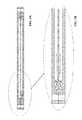
- FIG. 1shows a top view of an embodiment of a wafer susceptor
- FIGS. 2A and 2Bshow a side view and an enlarged side view, respectively, of an embodiment of a wafer susceptor
- FIG. 3shows a side view of an embodiment of a reactor with two sets of susceptor plates
- FIG. 4shows a top view of a batch stack reactor (BSR) embodiment
- FIGS. 5A and 5Bshow a side view and an enlarged side view, respectively, of an embodiment of a double-sided deposition (DSD) susceptor arrangement
- FIG. 6shows a top view of an embodiment comprising an array of susceptors
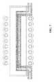
- FIG. 7shows a side view of an embodiment of a double-sided deposition reactor.
- the present disclosurereferences a “template,” which may be viewed as equivalent to a “wafer.”
- the templateafter epitaxy, may be used repeatedly to grow and release crystalline wafers. But the use to which the template or wafer is put after epitaxial deposition is beyond the scope of the present disclosure: one of ordinary skill will recognize the myriad uses to which the template might be put without departing from the spirit of the present disclosure.
- a susceptoris a material used for its ability to absorb electromagnetic energy and impart that energy, in the form of heat, to the wafers.
- the susceptorsmay be heated electromagnetically, lamps or resistive heating may also be effective.
- the susceptors of the present disclosuremay be stackable, yet they do not rely on stacking for providing the “building blocks” of the overall reactor.
- the reactors of the present disclosuremay or may not be depletion mode reactors (DMRs).
- DMRsdepletion mode reactors
- “Depletion mode”refers to the depletion or utilization of chemical along the direction of gas flow. As shown in FIG. 1 , that direction may be reversed to even out film thickness from one end to the other. In embodiments where the direction is not reversed, a tendency to deposit more chemicals in the region closest to the source port may be exhibited.
- port 10comprises a source port
- port 12comprises an exhaust port; in a reverse-flow mode, the opposite is true.
- port 10may be referred to as “source/exhaust port 10 ,” and port 12 may be referred to as “exhaust/source port 12 .”
- FIGS. 1 , 2 A, and 2 Bshow different views of the same susceptor arrangement: a top view, a side view, and a detail side view, respectively. As shown in FIGS. 2A and 2B , the design of ports 10 and 12 lends itself to the stackable nature of the wafer susceptors of the present disclosure.
- Baffle channels 15are shown in FIGS. 1 , 2 A, and 2 B. These baffle channels comprise a part of the path through which the TCS or other chemical species flows. Pin holes 16 , shown in FIG. 1 only, provide template lift during the epitaxial deposition process.
- template 20(shown in FIG. 2B ) is shown inserted into insert pocket 18 (shown in FIG. 1 ).
- the thickness of insert pocket 18is approximately 6 mm, and the length of the whole assembly is approximately 50 cm.
- the diameter of ports 10 and 12may be approximately 15 mm.
- FIG. 3shows reactor 30 , which includes two sets of stacked susceptor plates, similar to the susceptor plates shown in the preceding three FIGURES.
- the reactor of FIG. 3is a depletion mode reactor.
- Reactor 30includes source/exhaust port 40 and exhaust/source port 42 .
- the maid body of reactor 30is housed in quartz muffle 35 .
- reactor 30uses lamps 36 for heating the susceptor plates.
- hydrochloric acidHCl gas
- the concentration of HClcould continue to rise past the point of reaction inhibition and begin to etch the silicon template. While this is generally a state to be avoided, etching of silicon may be employed to clean the downstream exhaust passages. In effect, by allowing a sufficient level of HCl to build up, one could operate the reactor of the present disclosure in a self-maintaining mode by having the produced HCl gas etch away unwanted deposited silicon.
- FIG. 4shows reactor 50 , an embodiment of the present disclosure known as a batch stack reactor (BSR).
- BSRbatch stack reactor
- the susceptor platesare stacked to increase the batch load to, in some embodiments, several hundred wafers.
- H 2 gasBy purging the exterior of the susceptors with H 2 gas, the quartz bell jar is protected from silicon deposition.
- Most known bell jar reactorsare not protected from TCS and require periodic HCl cleaning to remove unwanted deposited silicon. This process may interrupt production, thereby adversely affecting the cost per wafer (i.e. CoO).
- Reactor 50is housed in quartz bell jar 52 .
- reactor 50includes separate ports for TCS and H 2 , although this is not a necessary feature of the present disclosure; in other embodiments, TCS and H 2 may be premixed and fed through the same ports.
- H 2 source/exhaust ports 54 and TCS source/exhaust ports 55are at one end of the reactor; H 2 exhaust/source ports 56 and TCS exhaust/source ports 57 are at the other end. These ports may be differentiated only when acting as source ports. When a given port is being used in an exhaust capacity, it will be exhausting gas that has already been mixed inside the reactor.
- FIG. 4shows an arrangement of separating the precursors until the point of use at each susceptor. This method may further extend chemical utilization and runtime favoring further improved CoO.
- each templateis exposed to process gases on both sides. This feature enables dual side deposition, which has a compounding effect of both increased chemical utilization and lower epi cost per wafer.
- FIGS. 5A and 5Bare generally similar in use to the ones shown in FIGS. 2A and 2B , and may be incorporated into various types of reactor configurations.
- the dual sided susceptorsmay be stackable (as shown in the embodiment of FIG. 3 ), yet they may also be arranged in a matrix as shown in FIG. 6 .
- FIG. 7shows a side view of a depletion mode reactor using the dual sided susceptors of FIGS. 5A and 5B . It is generally similar in structure to the reactor shown in FIG. 3 , but with a dual sided susceptor in place of the stacked susceptors.
Landscapes
- Chemical & Material Sciences (AREA)
- General Chemical & Material Sciences (AREA)
- Chemical Kinetics & Catalysis (AREA)
- Engineering & Computer Science (AREA)
- Materials Engineering (AREA)
- Metallurgy (AREA)
- Organic Chemistry (AREA)
- Mechanical Engineering (AREA)
- Crystallography & Structural Chemistry (AREA)
- Health & Medical Sciences (AREA)
- Toxicology (AREA)
- Chemical Vapour Deposition (AREA)
Abstract
Description
- This application claims priority to U.S. Provisional Patent Application Ser. No. 61/169,139, which is hereby incorporated by reference in its entirety.
- The present disclosure relates to epitaxial deposition. More particularly, the present disclosure relates to epitaxial deposition of silicon or other semiconducting materials.
- Monocrystalline silicon is the most dominant material for photovoltaic applications. The high efficiencies associated with monocrystalline solar cells, combined with the abundance of material, garner appeal for continued use and advancement. But the high processing cost of crystalline silicon material limits the widespread use of these solar modules. At present, the cost of “wafering,” or crystallizing silicon and cutting a wafer, accounts for about 40% finished solar cell cost. If a more direct way of making wafers were possible, great headway could be made in lowering the cost of solar cells.
- There are different known methods of growing monocrystalline silicon and releasing or transferring the grown wafer. Regardless of the method, a low cost epitaxial deposition process is assumed.
- Silicon epitaxial (epi) deposition was originally developed for the semiconductor industry. The requirements for the semiconductor industry, in both film properties and cost, are nearly polar opposites of requirements in the solar field. For example, semiconductor epi films are typically less than 5 μm (1 μm=10−6meter) thick, while solar requires 60-80 μm of silicon. In order to achieve economies in the solar industry, the silicon cost per watt must reside in the $0.25/watt or approximately $1.00/wafer (assuming a 4 watt cell).
- The precursor chemistry for epi is predominantly trichlorosilane (TCS), although for thinner films silane (SiH4) may also be used. Epitaxial deposition for each chemical poses unique requirements and challenges in both equipment architecture and process conditions. Based on low cost and abundance, TCS is the chemistry of choice for the solar industry. The present disclosure will generally be described with regard to TCS, but one of ordinary skill in the art will recognize its applications to silane and other precursor chemicals.
- In order to achieve the necessary economy for solar applications, process cost modeling is studied to identify and optimize equipment performance. Three categories of cost make up the total cost picture: fixed cost (FC), recurring cost (RC) and yield cost (YC). FC is made up of items such as equipment purchase price, installation cost, and robotics or automation cost. RC is largely made up of electricity, gases, chemicals, operator salaries, and maintenance technician support. YC may be interpreted as the total value of parts lost during production.
- To achieve the cost of ownership (CoO) numbers required by the solar field, all aspects of the cost picture must be optimized. The qualities of a low-cost process are (in order of priority): 1) high productivity, 2) high yield, 3) low RC, and 4) low FC.
- Designing highly productive equipment requires a good understanding of the process requirements and reflecting those requirements in the architecture. High yield requires a robust process and reliable equipment. Low RC turns out to be the dominant component in the cost model. RC can impact plant site selection based on, for example, cost of local power or availability of bulk chemicals. FC, although important, is diluted by equipment productivity.
- With the above said, in summary, a highly productive, reliable, efficient reactor may be essential for the production of low cost solar cells.
- Therefore, it is an object of the present disclosure to provide a CVD reactor having improved chemical utilization and high yield, and thereby reduce costs and improve efficiency.
- Achieving low RC requires efficient use of chemicals. In an effort to make use of a greater portion of TCS, a longer deposition zone will be described. Providing a longer deposition zone may allow a higher percentage of the TCS to be deposited. In this way, greater chemicals utilization may be realized. By choosing the optimal parameters (chemical concentration, gas speed, reaction dimensions, etc.), productivity and chemical utilization may be optimized. A further object of the present disclosure is minimization of deposition on surfaces other than the wafers, which is also important for effective chemical utilization. The disclosed reactor has a high wafer area to reactor surface area ratio, which tends to minimize parasitic losses.
- These and other advantages of the disclosed subject matter, as well as additional novel features, will be apparent from the description provided herein. The intent of this summary is not to be a comprehensive description of the subject matter, but rather to provide a short overview of some of the subject matter's functionality. Other systems, methods, features and advantages here provided will become apparent to one with skill in the art upon examination of the following FIGURES and detailed description. It is intended that all such additional systems, methods, features and advantages included within this description be within the scope of the claims.
- The features, nature, and advantages of the disclosed subject matter may become more apparent from the detailed description set forth below when taken in conjunction with the drawings in which like reference numerals indicate like features and wherein:
FIG. 1 shows a top view of an embodiment of a wafer susceptor;FIGS. 2A and 2B show a side view and an enlarged side view, respectively, of an embodiment of a wafer susceptor;FIG. 3 shows a side view of an embodiment of a reactor with two sets of susceptor plates;FIG. 4 shows a top view of a batch stack reactor (BSR) embodiment;FIGS. 5A and 5B show a side view and an enlarged side view, respectively, of an embodiment of a double-sided deposition (DSD) susceptor arrangement;FIG. 6 shows a top view of an embodiment comprising an array of susceptors; andFIG. 7 shows a side view of an embodiment of a double-sided deposition reactor.- Although the present disclosure is described with reference to specific embodiments, one skilled in the art could apply the principles discussed herein to other areas and/or embodiments without undue experimentation.
- The present disclosure references a “template,” which may be viewed as equivalent to a “wafer.” In one embodiment of the present disclosure, the template, after epitaxy, may be used repeatedly to grow and release crystalline wafers. But the use to which the template or wafer is put after epitaxial deposition is beyond the scope of the present disclosure: one of ordinary skill will recognize the myriad uses to which the template might be put without departing from the spirit of the present disclosure.
- One novel aspect of the reactor of the present disclosure lies in the arrangement of the wafer susceptors (a susceptor is a material used for its ability to absorb electromagnetic energy and impart that energy, in the form of heat, to the wafers). Although the susceptors may be heated electromagnetically, lamps or resistive heating may also be effective.
- The susceptors of the present disclosure may be stackable, yet they do not rely on stacking for providing the “building blocks” of the overall reactor. The reactors of the present disclosure may or may not be depletion mode reactors (DMRs). “Depletion mode” refers to the depletion or utilization of chemical along the direction of gas flow. As shown in
FIG. 1 , that direction may be reversed to even out film thickness from one end to the other. In embodiments where the direction is not reversed, a tendency to deposit more chemicals in the region closest to the source port may be exhibited. In a forward-flow (i.e. left-to-right) mode,port 10 comprises a source port, andport 12 comprises an exhaust port; in a reverse-flow mode, the opposite is true. For that reason,port 10 may be referred to as “source/exhaust port 10,” andport 12 may be referred to as “exhaust/source port 12.”FIGS. 1 ,2A, and2B show different views of the same susceptor arrangement: a top view, a side view, and a detail side view, respectively. As shown inFIGS. 2A and 2B , the design ofports Baffle channels 15 are shown inFIGS. 1 ,2A, and2B. These baffle channels comprise a part of the path through which the TCS or other chemical species flows. Pin holes16, shown inFIG. 1 only, provide template lift during the epitaxial deposition process.- In these views, template20 (shown in
FIG. 2B ) is shown inserted into insert pocket18 (shown inFIG. 1 ). - The various dimensions of the reactor shown may be varied by one of ordinary skill without departing from the spirit of the present invention.
- In this exemplary embodiment, the thickness of
insert pocket 18 is approximately 6 mm, and the length of the whole assembly is approximately 50 cm. The diameter ofports FIG. 3 showsreactor 30, which includes two sets of stacked susceptor plates, similar to the susceptor plates shown in the preceding three FIGURES. The reactor ofFIG. 3 is a depletion mode reactor.Reactor 30 includes source/exhaust port 40 and exhaust/source port 42. The maid body ofreactor 30 is housed inquartz muffle 35. As shown,reactor 30 useslamps 36 for heating the susceptor plates.- During the reaction (or reduction) of TCS with hydrogen gas, hydrochloric acid (HCl gas) is produced. In fact, if the reaction were fed with additional H2and allowed to extend over a longer zone or time, the concentration of HCl could continue to rise past the point of reaction inhibition and begin to etch the silicon template. While this is generally a state to be avoided, etching of silicon may be employed to clean the downstream exhaust passages. In effect, by allowing a sufficient level of HCl to build up, one could operate the reactor of the present disclosure in a self-maintaining mode by having the produced HCl gas etch away unwanted deposited silicon.
FIG. 4 showsreactor 50, an embodiment of the present disclosure known as a batch stack reactor (BSR). In this configuration, the susceptor plates are stacked to increase the batch load to, in some embodiments, several hundred wafers. By purging the exterior of the susceptors with H2gas, the quartz bell jar is protected from silicon deposition. Most known bell jar reactors are not protected from TCS and require periodic HCl cleaning to remove unwanted deposited silicon. This process may interrupt production, thereby adversely affecting the cost per wafer (i.e. CoO).Reactor 50 is housed inquartz bell jar 52. In the embodiment shown,reactor 50 includes separate ports for TCS and H2, although this is not a necessary feature of the present disclosure; in other embodiments, TCS and H2may be premixed and fed through the same ports. As shown, H2source/exhaust ports 54 and TCS source/exhaust ports 55 are at one end of the reactor; H2exhaust/source ports 56 and TCS exhaust/source ports 57 are at the other end. These ports may be differentiated only when acting as source ports. When a given port is being used in an exhaust capacity, it will be exhausting gas that has already been mixed inside the reactor.- TCS reduction with H2may result when the gases are mixed at the appropriate temperature.
FIG. 4 shows an arrangement of separating the precursors until the point of use at each susceptor. This method may further extend chemical utilization and runtime favoring further improved CoO. - In the arrangement shown in
FIGS. 5A and 5B , each template is exposed to process gases on both sides. This feature enables dual side deposition, which has a compounding effect of both increased chemical utilization and lower epi cost per wafer. - The susceptors shown in
FIGS. 5A and 5B are generally similar in use to the ones shown inFIGS. 2A and 2B , and may be incorporated into various types of reactor configurations. - The dual sided susceptors may be stackable (as shown in the embodiment of
FIG. 3 ), yet they may also be arranged in a matrix as shown inFIG. 6 . FIG. 7 shows a side view of a depletion mode reactor using the dual sided susceptors ofFIGS. 5A and 5B . It is generally similar in structure to the reactor shown inFIG. 3 , but with a dual sided susceptor in place of the stacked susceptors.- Those with ordinary skill in the art will recognize that the disclosed embodiments have relevance to a wide variety of areas in addition to those specific examples described above. In particular, any of the disclosed susceptors could be placed into any of the disclosed reactor arrangements without undue experimentation by one of ordinary skill in the art.
- The foregoing description of the exemplary embodiments is provided to enable any person skilled in the art to make or use the claimed subject matter. Various modifications to these embodiments will be readily apparent to those skilled in the art, and the generic principles defined herein may be applied to other embodiments without the use of the innovative faculty. Thus, the claimed subject matter is not intended to be limited to the embodiments shown herein but is to be accorded the widest scope consistent with the principles and novel features disclosed herein.
- It is intended that all such additional systems, methods, features, and advantages that are included within this description be within the scope of the claims.
Claims (20)
Priority Applications (5)
| Application Number | Priority Date | Filing Date | Title |
|---|---|---|---|
| CN201080021690.9ACN102427971B (en) | 2009-04-14 | 2010-04-14 | High efficiency epitaxial chemical vapor deposition (cvd) reactor |
| EP10765064.0AEP2419306B1 (en) | 2009-04-14 | 2010-04-14 | High efficiency epitaxial chemical vapor deposition (cvd) reactor |
| PCT/US2010/030991WO2010120850A1 (en) | 2009-04-14 | 2010-04-14 | High efficiency epitaxial chemical vapor deposition (cvd) reactor |
| US12/759,820US8656860B2 (en) | 2009-04-14 | 2010-04-14 | High efficiency epitaxial chemical vapor deposition (CVD) reactor |
| US13/341,965US20120192789A1 (en) | 2010-04-14 | 2011-12-31 | Deposition systems and processes |
Applications Claiming Priority (2)
| Application Number | Priority Date | Filing Date | Title |
|---|---|---|---|
| US16913909P | 2009-04-14 | 2009-04-14 | |
| US12/759,820US8656860B2 (en) | 2009-04-14 | 2010-04-14 | High efficiency epitaxial chemical vapor deposition (CVD) reactor |
Related Child Applications (1)
| Application Number | Title | Priority Date | Filing Date |
|---|---|---|---|
| US13/341,965Continuation-In-PartUS20120192789A1 (en) | 2010-04-14 | 2011-12-31 | Deposition systems and processes |
Publications (2)
| Publication Number | Publication Date |
|---|---|
| US20100267245A1true US20100267245A1 (en) | 2010-10-21 |
| US8656860B2 US8656860B2 (en) | 2014-02-25 |
Family
ID=42981324
Family Applications (1)
| Application Number | Title | Priority Date | Filing Date |
|---|---|---|---|
| US12/759,820Expired - Fee RelatedUS8656860B2 (en) | 2009-04-14 | 2010-04-14 | High efficiency epitaxial chemical vapor deposition (CVD) reactor |
Country Status (4)
| Country | Link |
|---|---|
| US (1) | US8656860B2 (en) |
| EP (1) | EP2419306B1 (en) |
| CN (1) | CN102427971B (en) |
| WO (1) | WO2010120850A1 (en) |
Cited By (21)
| Publication number | Priority date | Publication date | Assignee | Title |
|---|---|---|---|---|
| WO2012099700A1 (en)* | 2010-12-31 | 2012-07-26 | Solexel, Inc. | Deposition systems and processes |
| US8241940B2 (en) | 2010-02-12 | 2012-08-14 | Solexel, Inc. | Double-sided reusable template for fabrication of semiconductor substrates for photovoltaic cell and microelectronics device manufacturing |
| US8399331B2 (en) | 2007-10-06 | 2013-03-19 | Solexel | Laser processing for high-efficiency thin crystalline silicon solar cell fabrication |
| US8664737B2 (en) | 2008-11-13 | 2014-03-04 | Selexel, Inc. | Three-dimensional semiconductor template for making high efficiency thin-film solar cells |
| US8906218B2 (en) | 2010-05-05 | 2014-12-09 | Solexel, Inc. | Apparatus and methods for uniformly forming porous semiconductor on a substrate |
| US8946547B2 (en) | 2010-08-05 | 2015-02-03 | Solexel, Inc. | Backplane reinforcement and interconnects for solar cells |
| US8962380B2 (en) | 2009-12-09 | 2015-02-24 | Solexel, Inc. | High-efficiency photovoltaic back-contact solar cell structures and manufacturing methods using thin planar semiconductor absorbers |
| US20150152991A1 (en)* | 2013-11-29 | 2015-06-04 | Taiwan Semiconductor Manufacturing Co., Ltd. | Mechanisms for supplying process gas into wafer process apparatus |
| US9076642B2 (en) | 2009-01-15 | 2015-07-07 | Solexel, Inc. | High-Throughput batch porous silicon manufacturing equipment design and processing methods |
| US20150350669A1 (en)* | 2014-05-27 | 2015-12-03 | Thomas Licensing | Method and apparatus for improving estimation of disparity in a stereo image pair using a hybrid recursive matching processing |
| WO2015192105A1 (en)* | 2014-06-12 | 2015-12-17 | Crystal Solar, Inc. | Cvd epitaxial reactor chamber with resistive heating, three channel substrate carrier and gas preheat structure |
| US9318644B2 (en) | 2009-05-05 | 2016-04-19 | Solexel, Inc. | Ion implantation and annealing for thin film crystalline solar cells |
| US9349887B2 (en) | 2006-10-09 | 2016-05-24 | Solexel, Inc. | Three-dimensional thin-film solar cells |
| US9397250B2 (en) | 2006-10-09 | 2016-07-19 | Solexel, Inc. | Releasing apparatus for separating a semiconductor substrate from a semiconductor template |
| US9508886B2 (en) | 2007-10-06 | 2016-11-29 | Solexel, Inc. | Method for making a crystalline silicon solar cell substrate utilizing flat top laser beam |
| US9556522B2 (en) | 2009-02-25 | 2017-01-31 | Crystal Solar Incorporated | High throughput multi-wafer epitaxial reactor |
| US9748414B2 (en) | 2011-05-20 | 2017-08-29 | Arthur R. Zingher | Self-activated front surface bias for a solar cell |
| US9870937B2 (en) | 2010-06-09 | 2018-01-16 | Ob Realty, Llc | High productivity deposition reactor comprising a gas flow chamber having a tapered gas flow space |
| US9920451B2 (en) | 2009-02-25 | 2018-03-20 | Crystal Solar Incorporated | High throughput multi-wafer epitaxial reactor |
| US9982363B2 (en) | 2011-05-27 | 2018-05-29 | Crystal Solar, Incorporated | Silicon wafers by epitaxial deposition |
| US11166874B2 (en) | 2010-06-14 | 2021-11-09 | Trutag Technologies, Inc. | System for producing a packaged item with an identifier |
Families Citing this family (1)
| Publication number | Priority date | Publication date | Assignee | Title |
|---|---|---|---|---|
| KR101313262B1 (en) | 2010-07-12 | 2013-09-30 | 삼성전자주식회사 | Chemical Vapor Deposition Apparatus and Method of Forming Semiconductor Thin Film Using The Same |
Citations (97)
| Publication number | Priority date | Publication date | Assignee | Title |
|---|---|---|---|---|
| US4043894A (en)* | 1976-05-20 | 1977-08-23 | Burroughs Corporation | Electrochemical anodization fixture for semiconductor wafers |
| US4070206A (en)* | 1976-05-20 | 1978-01-24 | Rca Corporation | Polycrystalline or amorphous semiconductor photovoltaic device having improved collection efficiency |
| US4082570A (en)* | 1976-02-09 | 1978-04-04 | Semicon, Inc. | High intensity solar energy converter |
| US4165252A (en)* | 1976-08-30 | 1979-08-21 | Burroughs Corporation | Method for chemically treating a single side of a workpiece |
| US4249959A (en)* | 1979-11-28 | 1981-02-10 | Rca Corporation | Solar cell construction |
| US4251679A (en)* | 1979-03-16 | 1981-02-17 | E-Cel Corporation | Electromagnetic radiation transducer |
| US4348254A (en)* | 1978-12-27 | 1982-09-07 | Solarex Corporation | Method of making solar cell |
| US4361950A (en)* | 1980-03-24 | 1982-12-07 | Exxon Research & Engineering Co. | Method of making solar cell with wrap-around electrode |
| US4409423A (en)* | 1982-03-09 | 1983-10-11 | The United States Of America As Represented By The Secretary Of The Air Force | Hole matrix vertical junction solar cell |
| US4427839A (en)* | 1981-11-09 | 1984-01-24 | General Electric Company | Faceted low absorptance solar cell |
| US4461922A (en)* | 1983-02-14 | 1984-07-24 | Atlantic Richfield Company | Solar cell module |
| US4468283A (en)* | 1982-12-17 | 1984-08-28 | Irfan Ahmed | Method for etching and controlled chemical vapor deposition |
| US4479847A (en)* | 1981-12-30 | 1984-10-30 | California Institute Of Technology | Equilibrium crystal growth from substrate confined liquid |
| US4626613A (en)* | 1983-12-23 | 1986-12-02 | Unisearch Limited | Laser grooved solar cell |
| US4672023A (en)* | 1985-10-21 | 1987-06-09 | Avantek, Inc. | Method for planarizing wafers |
| US4922277A (en)* | 1988-11-28 | 1990-05-01 | The United States Of America As Represented By The Secretary Of The Air Force | Silicon wafer photoresist developer |
| US5024953A (en)* | 1988-03-22 | 1991-06-18 | Hitachi, Ltd. | Method for producing opto-electric transducing element |
| US5073230A (en)* | 1990-04-17 | 1991-12-17 | Arizona Board Of Regents Acting On Behalf Of Arizona State University | Means and methods of lifting and relocating an epitaxial device layer |
| US5112453A (en)* | 1990-10-31 | 1992-05-12 | Behr Omri M | Method and apparatus for producing etched plates for graphic printing |
| US5208068A (en)* | 1989-04-17 | 1993-05-04 | International Business Machines Corporation | Lamination method for coating the sidewall or filling a cavity in a substrate |
| US5248621A (en)* | 1990-10-23 | 1993-09-28 | Canon Kabushiki Kaisha | Method for producing solar cell devices of crystalline material |
| US5316593A (en)* | 1992-11-16 | 1994-05-31 | Midwest Research Institute | Heterojunction solar cell with passivated emitter surface |
| US5348618A (en)* | 1989-12-07 | 1994-09-20 | The Secretary Of State For Defence In Her Britannic Majesty's Government Of The United Kingdom Of Great Britain And Northern Ireland | Method of making silicon quantum wires |
| US5397400A (en)* | 1992-07-22 | 1995-03-14 | Mitsubishi Denki Kabushiki Kaisha | Thin-film solar cell |
| US5459099A (en)* | 1990-09-28 | 1995-10-17 | The United States Of America As Represented By The Secretary Of The Navy | Method of fabricating sub-half-micron trenches and holes |
| US5494832A (en)* | 1993-03-29 | 1996-02-27 | Siemens Aktiengesellschaft | Method for manufacturing a solar cell from a substrate wafer |
| US5538564A (en)* | 1994-03-18 | 1996-07-23 | Regents Of The University Of California | Three dimensional amorphous silicon/microcrystalline silicon solar cells |
| US5645684A (en)* | 1994-03-07 | 1997-07-08 | The Regents Of The University Of California | Multilayer high vertical aspect ratio thin film structures |
| US5660680A (en)* | 1994-03-07 | 1997-08-26 | The Regents Of The University Of California | Method for fabrication of high vertical aspect ratio thin film structures |
| US5681392A (en)* | 1995-12-21 | 1997-10-28 | Xerox Corporation | Fluid reservoir containing panels for reducing rate of fluid flow |
| US5882988A (en)* | 1995-08-16 | 1999-03-16 | Philips Electronics North America Corporation | Semiconductor chip-making without scribing |
| US5899360A (en)* | 1995-06-09 | 1999-05-04 | Colgate - Palmolive Company | Multi-chamber refillable dispenser |
| US5928438A (en)* | 1995-10-05 | 1999-07-27 | Ebara Solar, Inc. | Structure and fabrication process for self-aligned locally deep-diffused emitter (SALDE) solar cell |
| US6091021A (en)* | 1996-11-01 | 2000-07-18 | Sandia Corporation | Silicon cells made by self-aligned selective-emitter plasma-etchback process |
| US6096229A (en)* | 1998-07-30 | 2000-08-01 | Lucent Technologies Inc. | Method of making alignment grooves in an optical connector support member |
| US6114046A (en)* | 1997-07-24 | 2000-09-05 | Evergreen Solar, Inc. | Encapsulant material for solar cell module and laminated glass applications |
| US6127623A (en)* | 1998-07-03 | 2000-10-03 | Sharp Kabushiki Kaisha | Solar cell and production process therefor |
| US6204443B1 (en)* | 1997-06-09 | 2001-03-20 | Canon Kabushiki Kaisha | Solar cell module having a specific front side covering material and a process for the production of said solar cell module |
| US6294725B1 (en)* | 2000-03-31 | 2001-09-25 | Trw Inc. | Wireless solar cell array electrical interconnection scheme |
| US6399143B1 (en)* | 1996-04-09 | 2002-06-04 | Delsys Pharmaceutical Corporation | Method for clamping and electrostatically coating a substrate |
| US6416647B1 (en)* | 1998-04-21 | 2002-07-09 | Applied Materials, Inc. | Electro-chemical deposition cell for face-up processing of single semiconductor substrates |
| US6429037B1 (en)* | 1998-06-29 | 2002-08-06 | Unisearch Limited | Self aligning method for forming a selective emitter and metallization in a solar cell |
| US6441297B1 (en)* | 1998-03-13 | 2002-08-27 | Steffen Keller | Solar cell arrangement |
| US6448155B1 (en)* | 1999-06-17 | 2002-09-10 | Canon Kabushiki Kaisha | Production method of semiconductor base material and production method of solar cell |
| US6461932B1 (en)* | 1998-12-14 | 2002-10-08 | National Semiconductor Corporation | Semiconductor trench isolation process that utilizes smoothening layer |
| US20020153039A1 (en)* | 2001-04-23 | 2002-10-24 | In-Sik Moon | Solar cell and method for fabricating the same |
| US20020168592A1 (en)* | 2001-04-19 | 2002-11-14 | Vezenov Dmitri V. | Method of fabricating sub-micron hemispherical and hemicylidrical structures from non-spherically shaped templates |
| US20030017712A1 (en)* | 1997-06-30 | 2003-01-23 | Rolf Brendel | Method for producing layered structures on a substrate, substrate and semiconductor components produced according to said method |
| US20030039843A1 (en)* | 1997-03-14 | 2003-02-27 | Christopher Johnson | Photoactive coating, coated article, and method of making same |
| US6534336B1 (en)* | 1999-05-21 | 2003-03-18 | Canon Kabushiki Kaisha | Production method of photoelectric conversion device, and photoelectric conversion device produced by the method |
| US6555443B1 (en)* | 1998-11-11 | 2003-04-29 | Robert Bosch Gmbh | Method for production of a thin film and a thin-film solar cell, in particular, on a carrier substrate |
| US6566235B2 (en)* | 2000-03-31 | 2003-05-20 | Canon Kabushiki Kaisha | Process for producing semiconductor member, and process for producing solar cell |
| US20030124761A1 (en)* | 1997-03-28 | 2003-07-03 | Kris Baert | Method for depositing polycrystalline sige suitable for micromachining and devices obtained thereof |
| US6602767B2 (en)* | 2000-01-27 | 2003-08-05 | Canon Kabushiki Kaisha | Method for transferring porous layer, method for making semiconductor devices, and method for making solar battery |
| US6602760B2 (en)* | 2000-12-21 | 2003-08-05 | Interuniversitair Microelektronica Centrum (Imec) | Method of producing a semiconductor layer on a substrate |
| US6613148B1 (en)* | 1996-01-18 | 2003-09-02 | Micron Technology, Inc. | Method and apparatus for applying highly viscous liquid to substrate |
| US6624009B1 (en)* | 1996-11-06 | 2003-09-23 | Pacific Solar Pty Limited | Forming a crystalline semiconductor film on a glass substrate |
| US6649485B2 (en)* | 2000-03-09 | 2003-11-18 | Interuniversitair Microelektronica Centrum (Imec) | Method for the formation and lift-off of porous silicon layers |
| US6653722B2 (en)* | 2000-08-29 | 2003-11-25 | Micron Technology, Inc. | Method for applying uniform pressurized film across wafer |
| US20040028875A1 (en)* | 2000-12-02 | 2004-02-12 | Van Rijn Cornelis Johannes Maria | Method of making a product with a micro or nano sized structure and product |
| US6756289B1 (en)* | 1996-12-27 | 2004-06-29 | Canon Kabushiki Kaisha | Method of producing semiconductor member and method of producing solar cell |
| US20040175893A1 (en)* | 2003-03-07 | 2004-09-09 | Applied Materials, Inc. | Apparatuses and methods for forming a substantially facet-free epitaxial film |
| US20040173790A1 (en)* | 2003-03-05 | 2004-09-09 | Yee-Chia Yeo | Method of forming strained silicon on insulator substrate |
| US6881644B2 (en)* | 1999-04-21 | 2005-04-19 | Silicon Genesis Corporation | Smoothing method for cleaved films made using a release layer |
| US20050160970A1 (en)* | 2003-12-25 | 2005-07-28 | Kyocera Corporation | Photovoltaic conversion device and method of manufacturing the device |
| US20050176164A1 (en)* | 2004-02-05 | 2005-08-11 | Advent Solar, Inc. | Back-contact solar cells and methods for fabrication |
| US20050177343A1 (en)* | 2004-01-15 | 2005-08-11 | Nobuaki Nagae | Method and apparatus for forming a pattern, device and electronic apparatus |
| US20050172998A1 (en)* | 2004-02-05 | 2005-08-11 | Advent Solar, Inc. | Buried-contact solar cells with self-doping contacts |
| US20050199279A1 (en)* | 2004-01-29 | 2005-09-15 | Sanyo Electric Co., Ltd. | Solar cell module |
| US6946052B2 (en)* | 2001-05-25 | 2005-09-20 | Canon Kabushiki Kaisha | Separating apparatus and processing method for plate member |
| US6964732B2 (en)* | 2000-03-09 | 2005-11-15 | Interuniversitair Microelektronica Centrum (Imec) | Method and apparatus for continuous formation and lift-off of porous silicon layers |
| US20060021565A1 (en)* | 2004-07-30 | 2006-02-02 | Aonex Technologies, Inc. | GaInP / GaAs / Si triple junction solar cell enabled by wafer bonding and layer transfer |
| US20060043495A1 (en)* | 2002-07-19 | 2006-03-02 | Renesas Technology Corp. | Semiconductor device |
| US20060054212A1 (en)* | 2004-09-10 | 2006-03-16 | Fraas Lewis M | Solar photovoltaic mirror modules |
| US7022585B2 (en)* | 2002-07-24 | 2006-04-04 | Interuniversitair Microelektronica Centrum (Imec) | Method for making thin film devices intended for solar cells or silicon-on-insulator (SOI) applications |
| US20060070884A1 (en)* | 2004-10-06 | 2006-04-06 | Kazutaka Momoi | Electrochemical processing apparatus and method |
| US7026237B2 (en)* | 1999-08-26 | 2006-04-11 | Brewer Science Inc. | Fill material for dual damascene processes |
| US20060105492A1 (en)* | 2002-08-06 | 2006-05-18 | Janos Veres | Organic electronic devices |
| US20060196536A1 (en)* | 2005-03-07 | 2006-09-07 | Sharp Kabushiki Kaisha | Thin film solar cell and manufacturing method thereof |
| US20060231031A1 (en)* | 2002-12-12 | 2006-10-19 | Otb Group B.V. | Method and apparatus for treating a substrate |
| US20060252243A1 (en)* | 2005-04-20 | 2006-11-09 | Fuji Electric Holdings Co., Ltd. | Epitaxial film deposition system and epitaxial film formation method |
| US20060266916A1 (en)* | 2005-05-25 | 2006-11-30 | Molecular Imprints, Inc. | Imprint lithography template having a coating to reflect and/or absorb actinic energy |
| US7147714B2 (en)* | 2000-12-12 | 2006-12-12 | Denso Corporation | Manufacturing method of silicon carbide single crystals |
| US20070077770A1 (en)* | 2005-09-30 | 2007-04-05 | Molecular Imprints, Inc. | Etching technique to planarize a multi-layer structure |
| US20070082499A1 (en)* | 2005-10-11 | 2007-04-12 | Samsung Electronics Co., Ltd. | Photoresist coating apparatus, medium, and method efficiently spraying photoresist |
| US20080047601A1 (en)* | 2006-08-22 | 2008-02-28 | Somnath Nag | High Efficiency Solar Cells and Manufacturing Methods |
| US7368756B2 (en)* | 2002-07-19 | 2008-05-06 | Cree, Inc. | Trench cut light emitting diodes and methods of fabricating same |
| US20080157283A1 (en)* | 2006-10-09 | 2008-07-03 | Mehrdad Moslehi | Template for three-dimensional thin-film solar cell manufacturing and methods of use |
| US7402523B2 (en)* | 2005-03-31 | 2008-07-22 | Tokyo Electron Limited | Etching method |
| US20080210294A1 (en)* | 2006-10-09 | 2008-09-04 | Mehrdad Moslehi | Solar module structures and assembly methods for pyramidal three-dimensional thin-film solar cells |
| US20080241384A1 (en)* | 2007-04-02 | 2008-10-02 | Asm Genitech Korea Ltd. | Lateral flow deposition apparatus and method of depositing film by using the apparatus |
| US20080264477A1 (en)* | 2006-10-09 | 2008-10-30 | Soltaix, Inc. | Methods for manufacturing three-dimensional thin-film solar cells |
| US20080289684A1 (en)* | 2006-10-09 | 2008-11-27 | Soltaix, Inc. | Pyramidal three-dimensional thin-film solar cells |
| US20090042320A1 (en)* | 2006-10-09 | 2009-02-12 | Solexel, Inc. | Methods for liquid transfer coating of three-dimensional substrates |
| US7648927B2 (en)* | 2005-06-21 | 2010-01-19 | Applied Materials, Inc. | Method for forming silicon-containing materials during a photoexcitation deposition process |
| US20100022074A1 (en)* | 2008-05-28 | 2010-01-28 | Solexel, Inc. | Substrate release methods and apparatuses |
| US20100116316A1 (en)* | 2008-11-26 | 2010-05-13 | Solexel, Inc. | Truncated pyramid structures for see-through solar cells |
Family Cites Families (14)
| Publication number | Priority date | Publication date | Assignee | Title |
|---|---|---|---|---|
| FR2763964B1 (en) | 1997-05-28 | 1999-08-13 | Sgs Thomson Microelectronics | IMPROVEMENT OF THE GAS FLOW IN AN EPITAXY REACTOR |
| US6331208B1 (en) | 1998-05-15 | 2001-12-18 | Canon Kabushiki Kaisha | Process for producing solar cell, process for producing thin-film semiconductor, process for separating thin-film semiconductor, and process for forming semiconductor |
| US6664169B1 (en) | 1999-06-08 | 2003-12-16 | Canon Kabushiki Kaisha | Process for producing semiconductor member, process for producing solar cell, and anodizing apparatus |
| JP2003052185A (en) | 2001-05-30 | 2003-02-21 | Canon Inc | Power converter, photovoltaic element module using the same, and power generator |
| WO2003037798A1 (en) | 2001-10-30 | 2003-05-08 | Catalysts & Chemicals Industries Co., Ltd. | Tubular titanium oxide particles, method for preparing the same, and use of the same |
| US20030159652A1 (en)* | 2002-02-25 | 2003-08-28 | United Microelectronics Corp. | Heating injection apparatus for vapor liquid delivery system |
| EP2251911B1 (en) | 2002-10-25 | 2017-11-29 | Nakajima Glass Co., Inc. | Solar battery module manufacturing method |
| GB0227902D0 (en) | 2002-11-29 | 2003-01-08 | Ingenia Holdings Ltd | Template |
| US7312440B2 (en) | 2003-01-14 | 2007-12-25 | Georgia Tech Research Corporation | Integrated micro fuel processor and flow delivery infrastructure |
| US7402448B2 (en) | 2003-01-31 | 2008-07-22 | Bp Corporation North America Inc. | Photovoltaic cell and production thereof |
| CN1276474C (en)* | 2003-04-18 | 2006-09-20 | 联华电子股份有限公司 | Method for Improving Wafer Surface Flatness |
| GB0510051D0 (en) | 2005-05-17 | 2005-06-22 | Forticrete Ltd | Interlocking roof tiles |
| US20070095386A1 (en) | 2005-06-06 | 2007-05-03 | Solaria Corporation | Method and system for integrated solar cell using a plurality of photovoltaic regions |
| US7999174B2 (en) | 2006-10-09 | 2011-08-16 | Solexel, Inc. | Solar module structures and assembly methods for three-dimensional thin-film solar cells |
- 2010
- 2010-04-14WOPCT/US2010/030991patent/WO2010120850A1/enactiveApplication Filing
- 2010-04-14EPEP10765064.0Apatent/EP2419306B1/ennot_activeNot-in-force
- 2010-04-14CNCN201080021690.9Apatent/CN102427971B/ennot_activeExpired - Fee Related
- 2010-04-14USUS12/759,820patent/US8656860B2/ennot_activeExpired - Fee Related
Patent Citations (100)
| Publication number | Priority date | Publication date | Assignee | Title |
|---|---|---|---|---|
| US4082570A (en)* | 1976-02-09 | 1978-04-04 | Semicon, Inc. | High intensity solar energy converter |
| US4070206A (en)* | 1976-05-20 | 1978-01-24 | Rca Corporation | Polycrystalline or amorphous semiconductor photovoltaic device having improved collection efficiency |
| US4043894A (en)* | 1976-05-20 | 1977-08-23 | Burroughs Corporation | Electrochemical anodization fixture for semiconductor wafers |
| US4165252A (en)* | 1976-08-30 | 1979-08-21 | Burroughs Corporation | Method for chemically treating a single side of a workpiece |
| US4348254A (en)* | 1978-12-27 | 1982-09-07 | Solarex Corporation | Method of making solar cell |
| US4251679A (en)* | 1979-03-16 | 1981-02-17 | E-Cel Corporation | Electromagnetic radiation transducer |
| US4249959A (en)* | 1979-11-28 | 1981-02-10 | Rca Corporation | Solar cell construction |
| US4361950A (en)* | 1980-03-24 | 1982-12-07 | Exxon Research & Engineering Co. | Method of making solar cell with wrap-around electrode |
| US4427839A (en)* | 1981-11-09 | 1984-01-24 | General Electric Company | Faceted low absorptance solar cell |
| US4479847A (en)* | 1981-12-30 | 1984-10-30 | California Institute Of Technology | Equilibrium crystal growth from substrate confined liquid |
| US4409423A (en)* | 1982-03-09 | 1983-10-11 | The United States Of America As Represented By The Secretary Of The Air Force | Hole matrix vertical junction solar cell |
| US4468283A (en)* | 1982-12-17 | 1984-08-28 | Irfan Ahmed | Method for etching and controlled chemical vapor deposition |
| US4461922A (en)* | 1983-02-14 | 1984-07-24 | Atlantic Richfield Company | Solar cell module |
| US4626613A (en)* | 1983-12-23 | 1986-12-02 | Unisearch Limited | Laser grooved solar cell |
| US4672023A (en)* | 1985-10-21 | 1987-06-09 | Avantek, Inc. | Method for planarizing wafers |
| US5024953A (en)* | 1988-03-22 | 1991-06-18 | Hitachi, Ltd. | Method for producing opto-electric transducing element |
| US4922277A (en)* | 1988-11-28 | 1990-05-01 | The United States Of America As Represented By The Secretary Of The Air Force | Silicon wafer photoresist developer |
| US5208068A (en)* | 1989-04-17 | 1993-05-04 | International Business Machines Corporation | Lamination method for coating the sidewall or filling a cavity in a substrate |
| US5348618A (en)* | 1989-12-07 | 1994-09-20 | The Secretary Of State For Defence In Her Britannic Majesty's Government Of The United Kingdom Of Great Britain And Northern Ireland | Method of making silicon quantum wires |
| US5073230A (en)* | 1990-04-17 | 1991-12-17 | Arizona Board Of Regents Acting On Behalf Of Arizona State University | Means and methods of lifting and relocating an epitaxial device layer |
| US5459099A (en)* | 1990-09-28 | 1995-10-17 | The United States Of America As Represented By The Secretary Of The Navy | Method of fabricating sub-half-micron trenches and holes |
| US5248621A (en)* | 1990-10-23 | 1993-09-28 | Canon Kabushiki Kaisha | Method for producing solar cell devices of crystalline material |
| US5112453A (en)* | 1990-10-31 | 1992-05-12 | Behr Omri M | Method and apparatus for producing etched plates for graphic printing |
| US5397400A (en)* | 1992-07-22 | 1995-03-14 | Mitsubishi Denki Kabushiki Kaisha | Thin-film solar cell |
| US5316593A (en)* | 1992-11-16 | 1994-05-31 | Midwest Research Institute | Heterojunction solar cell with passivated emitter surface |
| US5494832A (en)* | 1993-03-29 | 1996-02-27 | Siemens Aktiengesellschaft | Method for manufacturing a solar cell from a substrate wafer |
| US5645684A (en)* | 1994-03-07 | 1997-07-08 | The Regents Of The University Of California | Multilayer high vertical aspect ratio thin film structures |
| US5660680A (en)* | 1994-03-07 | 1997-08-26 | The Regents Of The University Of California | Method for fabrication of high vertical aspect ratio thin film structures |
| US5538564A (en)* | 1994-03-18 | 1996-07-23 | Regents Of The University Of California | Three dimensional amorphous silicon/microcrystalline silicon solar cells |
| US5899360A (en)* | 1995-06-09 | 1999-05-04 | Colgate - Palmolive Company | Multi-chamber refillable dispenser |
| US5882988A (en)* | 1995-08-16 | 1999-03-16 | Philips Electronics North America Corporation | Semiconductor chip-making without scribing |
| US5928438A (en)* | 1995-10-05 | 1999-07-27 | Ebara Solar, Inc. | Structure and fabrication process for self-aligned locally deep-diffused emitter (SALDE) solar cell |
| US5681392A (en)* | 1995-12-21 | 1997-10-28 | Xerox Corporation | Fluid reservoir containing panels for reducing rate of fluid flow |
| US6613148B1 (en)* | 1996-01-18 | 2003-09-02 | Micron Technology, Inc. | Method and apparatus for applying highly viscous liquid to substrate |
| US6399143B1 (en)* | 1996-04-09 | 2002-06-04 | Delsys Pharmaceutical Corporation | Method for clamping and electrostatically coating a substrate |
| US6091021A (en)* | 1996-11-01 | 2000-07-18 | Sandia Corporation | Silicon cells made by self-aligned selective-emitter plasma-etchback process |
| US6624009B1 (en)* | 1996-11-06 | 2003-09-23 | Pacific Solar Pty Limited | Forming a crystalline semiconductor film on a glass substrate |
| US6756289B1 (en)* | 1996-12-27 | 2004-06-29 | Canon Kabushiki Kaisha | Method of producing semiconductor member and method of producing solar cell |
| US20030039843A1 (en)* | 1997-03-14 | 2003-02-27 | Christopher Johnson | Photoactive coating, coated article, and method of making same |
| US20030124761A1 (en)* | 1997-03-28 | 2003-07-03 | Kris Baert | Method for depositing polycrystalline sige suitable for micromachining and devices obtained thereof |
| US6204443B1 (en)* | 1997-06-09 | 2001-03-20 | Canon Kabushiki Kaisha | Solar cell module having a specific front side covering material and a process for the production of said solar cell module |
| US20030017712A1 (en)* | 1997-06-30 | 2003-01-23 | Rolf Brendel | Method for producing layered structures on a substrate, substrate and semiconductor components produced according to said method |
| US6645833B2 (en)* | 1997-06-30 | 2003-11-11 | Max-Planck-Gesellschaft Zur Foerderung Der Wissenschaften E. V. | Method for producing layered structures on a substrate, substrate and semiconductor components produced according to said method |
| US6114046A (en)* | 1997-07-24 | 2000-09-05 | Evergreen Solar, Inc. | Encapsulant material for solar cell module and laminated glass applications |
| US6441297B1 (en)* | 1998-03-13 | 2002-08-27 | Steffen Keller | Solar cell arrangement |
| US6416647B1 (en)* | 1998-04-21 | 2002-07-09 | Applied Materials, Inc. | Electro-chemical deposition cell for face-up processing of single semiconductor substrates |
| US6429037B1 (en)* | 1998-06-29 | 2002-08-06 | Unisearch Limited | Self aligning method for forming a selective emitter and metallization in a solar cell |
| US6127623A (en)* | 1998-07-03 | 2000-10-03 | Sharp Kabushiki Kaisha | Solar cell and production process therefor |
| US6096229A (en)* | 1998-07-30 | 2000-08-01 | Lucent Technologies Inc. | Method of making alignment grooves in an optical connector support member |
| US6555443B1 (en)* | 1998-11-11 | 2003-04-29 | Robert Bosch Gmbh | Method for production of a thin film and a thin-film solar cell, in particular, on a carrier substrate |
| US6461932B1 (en)* | 1998-12-14 | 2002-10-08 | National Semiconductor Corporation | Semiconductor trench isolation process that utilizes smoothening layer |
| US6881644B2 (en)* | 1999-04-21 | 2005-04-19 | Silicon Genesis Corporation | Smoothing method for cleaved films made using a release layer |
| US6534336B1 (en)* | 1999-05-21 | 2003-03-18 | Canon Kabushiki Kaisha | Production method of photoelectric conversion device, and photoelectric conversion device produced by the method |
| US6448155B1 (en)* | 1999-06-17 | 2002-09-10 | Canon Kabushiki Kaisha | Production method of semiconductor base material and production method of solar cell |
| US7026237B2 (en)* | 1999-08-26 | 2006-04-11 | Brewer Science Inc. | Fill material for dual damascene processes |
| US6602767B2 (en)* | 2000-01-27 | 2003-08-05 | Canon Kabushiki Kaisha | Method for transferring porous layer, method for making semiconductor devices, and method for making solar battery |
| US6964732B2 (en)* | 2000-03-09 | 2005-11-15 | Interuniversitair Microelektronica Centrum (Imec) | Method and apparatus for continuous formation and lift-off of porous silicon layers |
| US6649485B2 (en)* | 2000-03-09 | 2003-11-18 | Interuniversitair Microelektronica Centrum (Imec) | Method for the formation and lift-off of porous silicon layers |
| US6294725B1 (en)* | 2000-03-31 | 2001-09-25 | Trw Inc. | Wireless solar cell array electrical interconnection scheme |
| US6566235B2 (en)* | 2000-03-31 | 2003-05-20 | Canon Kabushiki Kaisha | Process for producing semiconductor member, and process for producing solar cell |
| US6653722B2 (en)* | 2000-08-29 | 2003-11-25 | Micron Technology, Inc. | Method for applying uniform pressurized film across wafer |
| US20040028875A1 (en)* | 2000-12-02 | 2004-02-12 | Van Rijn Cornelis Johannes Maria | Method of making a product with a micro or nano sized structure and product |
| US7147714B2 (en)* | 2000-12-12 | 2006-12-12 | Denso Corporation | Manufacturing method of silicon carbide single crystals |
| US6602760B2 (en)* | 2000-12-21 | 2003-08-05 | Interuniversitair Microelektronica Centrum (Imec) | Method of producing a semiconductor layer on a substrate |
| US20020168592A1 (en)* | 2001-04-19 | 2002-11-14 | Vezenov Dmitri V. | Method of fabricating sub-micron hemispherical and hemicylidrical structures from non-spherically shaped templates |
| US20020153039A1 (en)* | 2001-04-23 | 2002-10-24 | In-Sik Moon | Solar cell and method for fabricating the same |
| US6524880B2 (en)* | 2001-04-23 | 2003-02-25 | Samsung Sdi Co., Ltd. | Solar cell and method for fabricating the same |
| US6946052B2 (en)* | 2001-05-25 | 2005-09-20 | Canon Kabushiki Kaisha | Separating apparatus and processing method for plate member |
| US20060043495A1 (en)* | 2002-07-19 | 2006-03-02 | Renesas Technology Corp. | Semiconductor device |
| US7368756B2 (en)* | 2002-07-19 | 2008-05-06 | Cree, Inc. | Trench cut light emitting diodes and methods of fabricating same |
| US7022585B2 (en)* | 2002-07-24 | 2006-04-04 | Interuniversitair Microelektronica Centrum (Imec) | Method for making thin film devices intended for solar cells or silicon-on-insulator (SOI) applications |
| US20060105492A1 (en)* | 2002-08-06 | 2006-05-18 | Janos Veres | Organic electronic devices |
| US20060231031A1 (en)* | 2002-12-12 | 2006-10-19 | Otb Group B.V. | Method and apparatus for treating a substrate |
| US20040173790A1 (en)* | 2003-03-05 | 2004-09-09 | Yee-Chia Yeo | Method of forming strained silicon on insulator substrate |
| US20040175893A1 (en)* | 2003-03-07 | 2004-09-09 | Applied Materials, Inc. | Apparatuses and methods for forming a substantially facet-free epitaxial film |
| US20050160970A1 (en)* | 2003-12-25 | 2005-07-28 | Kyocera Corporation | Photovoltaic conversion device and method of manufacturing the device |
| US20050177343A1 (en)* | 2004-01-15 | 2005-08-11 | Nobuaki Nagae | Method and apparatus for forming a pattern, device and electronic apparatus |
| US20050199279A1 (en)* | 2004-01-29 | 2005-09-15 | Sanyo Electric Co., Ltd. | Solar cell module |
| US20050172998A1 (en)* | 2004-02-05 | 2005-08-11 | Advent Solar, Inc. | Buried-contact solar cells with self-doping contacts |
| US20050176164A1 (en)* | 2004-02-05 | 2005-08-11 | Advent Solar, Inc. | Back-contact solar cells and methods for fabrication |
| US20060021565A1 (en)* | 2004-07-30 | 2006-02-02 | Aonex Technologies, Inc. | GaInP / GaAs / Si triple junction solar cell enabled by wafer bonding and layer transfer |
| US20060054212A1 (en)* | 2004-09-10 | 2006-03-16 | Fraas Lewis M | Solar photovoltaic mirror modules |
| US20060070884A1 (en)* | 2004-10-06 | 2006-04-06 | Kazutaka Momoi | Electrochemical processing apparatus and method |
| US20060196536A1 (en)* | 2005-03-07 | 2006-09-07 | Sharp Kabushiki Kaisha | Thin film solar cell and manufacturing method thereof |
| US7402523B2 (en)* | 2005-03-31 | 2008-07-22 | Tokyo Electron Limited | Etching method |
| US20060252243A1 (en)* | 2005-04-20 | 2006-11-09 | Fuji Electric Holdings Co., Ltd. | Epitaxial film deposition system and epitaxial film formation method |
| US20060266916A1 (en)* | 2005-05-25 | 2006-11-30 | Molecular Imprints, Inc. | Imprint lithography template having a coating to reflect and/or absorb actinic energy |
| US7648927B2 (en)* | 2005-06-21 | 2010-01-19 | Applied Materials, Inc. | Method for forming silicon-containing materials during a photoexcitation deposition process |
| US20070077770A1 (en)* | 2005-09-30 | 2007-04-05 | Molecular Imprints, Inc. | Etching technique to planarize a multi-layer structure |
| US20070082499A1 (en)* | 2005-10-11 | 2007-04-12 | Samsung Electronics Co., Ltd. | Photoresist coating apparatus, medium, and method efficiently spraying photoresist |
| US20080047601A1 (en)* | 2006-08-22 | 2008-02-28 | Somnath Nag | High Efficiency Solar Cells and Manufacturing Methods |
| US20080157283A1 (en)* | 2006-10-09 | 2008-07-03 | Mehrdad Moslehi | Template for three-dimensional thin-film solar cell manufacturing and methods of use |
| US20080264477A1 (en)* | 2006-10-09 | 2008-10-30 | Soltaix, Inc. | Methods for manufacturing three-dimensional thin-film solar cells |
| US20080289684A1 (en)* | 2006-10-09 | 2008-11-27 | Soltaix, Inc. | Pyramidal three-dimensional thin-film solar cells |
| US20090042320A1 (en)* | 2006-10-09 | 2009-02-12 | Solexel, Inc. | Methods for liquid transfer coating of three-dimensional substrates |
| US20090107545A1 (en)* | 2006-10-09 | 2009-04-30 | Soltaix, Inc. | Template for pyramidal three-dimensional thin-film solar cell manufacturing and methods of use |
| US20080210294A1 (en)* | 2006-10-09 | 2008-09-04 | Mehrdad Moslehi | Solar module structures and assembly methods for pyramidal three-dimensional thin-film solar cells |
| US20080241384A1 (en)* | 2007-04-02 | 2008-10-02 | Asm Genitech Korea Ltd. | Lateral flow deposition apparatus and method of depositing film by using the apparatus |
| US20100022074A1 (en)* | 2008-05-28 | 2010-01-28 | Solexel, Inc. | Substrate release methods and apparatuses |
| US20100116316A1 (en)* | 2008-11-26 | 2010-05-13 | Solexel, Inc. | Truncated pyramid structures for see-through solar cells |
Cited By (26)
| Publication number | Priority date | Publication date | Assignee | Title |
|---|---|---|---|---|
| US9397250B2 (en) | 2006-10-09 | 2016-07-19 | Solexel, Inc. | Releasing apparatus for separating a semiconductor substrate from a semiconductor template |
| US9349887B2 (en) | 2006-10-09 | 2016-05-24 | Solexel, Inc. | Three-dimensional thin-film solar cells |
| US8399331B2 (en) | 2007-10-06 | 2013-03-19 | Solexel | Laser processing for high-efficiency thin crystalline silicon solar cell fabrication |
| US9508886B2 (en) | 2007-10-06 | 2016-11-29 | Solexel, Inc. | Method for making a crystalline silicon solar cell substrate utilizing flat top laser beam |
| US8664737B2 (en) | 2008-11-13 | 2014-03-04 | Selexel, Inc. | Three-dimensional semiconductor template for making high efficiency thin-film solar cells |
| US9076642B2 (en) | 2009-01-15 | 2015-07-07 | Solexel, Inc. | High-Throughput batch porous silicon manufacturing equipment design and processing methods |
| US10829864B2 (en) | 2009-01-15 | 2020-11-10 | Trutag Technologies, Inc. | Apparatus and methods for uniformly forming porous semiconductor on a substrate |
| US9556522B2 (en) | 2009-02-25 | 2017-01-31 | Crystal Solar Incorporated | High throughput multi-wafer epitaxial reactor |
| US9920451B2 (en) | 2009-02-25 | 2018-03-20 | Crystal Solar Incorporated | High throughput multi-wafer epitaxial reactor |
| US9318644B2 (en) | 2009-05-05 | 2016-04-19 | Solexel, Inc. | Ion implantation and annealing for thin film crystalline solar cells |
| US8962380B2 (en) | 2009-12-09 | 2015-02-24 | Solexel, Inc. | High-efficiency photovoltaic back-contact solar cell structures and manufacturing methods using thin planar semiconductor absorbers |
| US8241940B2 (en) | 2010-02-12 | 2012-08-14 | Solexel, Inc. | Double-sided reusable template for fabrication of semiconductor substrates for photovoltaic cell and microelectronics device manufacturing |
| US9401276B2 (en) | 2010-02-12 | 2016-07-26 | Solexel, Inc. | Apparatus for forming porous silicon layers on at least two surfaces of a plurality of silicon templates |
| US8906218B2 (en) | 2010-05-05 | 2014-12-09 | Solexel, Inc. | Apparatus and methods for uniformly forming porous semiconductor on a substrate |
| US9870937B2 (en) | 2010-06-09 | 2018-01-16 | Ob Realty, Llc | High productivity deposition reactor comprising a gas flow chamber having a tapered gas flow space |
| US11166874B2 (en) | 2010-06-14 | 2021-11-09 | Trutag Technologies, Inc. | System for producing a packaged item with an identifier |
| US8946547B2 (en) | 2010-08-05 | 2015-02-03 | Solexel, Inc. | Backplane reinforcement and interconnects for solar cells |
| WO2012099700A1 (en)* | 2010-12-31 | 2012-07-26 | Solexel, Inc. | Deposition systems and processes |
| KR101368598B1 (en) | 2010-12-31 | 2014-03-05 | 솔렉셀, 인크. | Deposition systems and processes |
| US9748414B2 (en) | 2011-05-20 | 2017-08-29 | Arthur R. Zingher | Self-activated front surface bias for a solar cell |
| US9982363B2 (en) | 2011-05-27 | 2018-05-29 | Crystal Solar, Incorporated | Silicon wafers by epitaxial deposition |
| US20150152991A1 (en)* | 2013-11-29 | 2015-06-04 | Taiwan Semiconductor Manufacturing Co., Ltd. | Mechanisms for supplying process gas into wafer process apparatus |
| US11414759B2 (en)* | 2013-11-29 | 2022-08-16 | Taiwan Semiconductor Manufacturing Co., Ltd | Mechanisms for supplying process gas into wafer process apparatus |
| US12359318B2 (en) | 2013-11-29 | 2025-07-15 | Taiwan Semiconductor Manufacturing Company, Ltd. | Mechanisms for supplying process gas into wafer process apparatus |
| US20150350669A1 (en)* | 2014-05-27 | 2015-12-03 | Thomas Licensing | Method and apparatus for improving estimation of disparity in a stereo image pair using a hybrid recursive matching processing |
| WO2015192105A1 (en)* | 2014-06-12 | 2015-12-17 | Crystal Solar, Inc. | Cvd epitaxial reactor chamber with resistive heating, three channel substrate carrier and gas preheat structure |
Also Published As
| Publication number | Publication date |
|---|---|
| CN102427971A (en) | 2012-04-25 |
| EP2419306A1 (en) | 2012-02-22 |
| US8656860B2 (en) | 2014-02-25 |
| EP2419306A4 (en) | 2013-01-02 |
| EP2419306B1 (en) | 2016-03-30 |
| CN102427971B (en) | 2015-01-07 |
| WO2010120850A1 (en) | 2010-10-21 |
Similar Documents
| Publication | Publication Date | Title |
|---|---|---|
| US8656860B2 (en) | High efficiency epitaxial chemical vapor deposition (CVD) reactor | |
| US11041253B2 (en) | Silicon wafers by epitaxial deposition | |
| US20120192789A1 (en) | Deposition systems and processes | |
| US9870937B2 (en) | High productivity deposition reactor comprising a gas flow chamber having a tapered gas flow space | |
| JP5555241B2 (en) | Apparatus for material deposition, system for material deposition and method for material deposition | |
| US9441295B2 (en) | Multi-channel gas-delivery system | |
| US8968473B2 (en) | Stackable multi-port gas nozzles | |
| US8652259B2 (en) | Scalable, high-throughput, multi-chamber epitaxial reactor for silicon deposition | |
| CN104025304A (en) | Buffer layer for improving the performance and stability of surface passivation of si solar cells | |
| KR20110101227A (en) | Dry Cleaning of Silicon Surfaces for Solar Cell Applications | |
| US8562745B2 (en) | Stable wafer-carrier system | |
| CN102738248B (en) | Optoelectronic device and method for manufacturing thereof | |
| CN117457777A (en) | A solar cell and its preparation method and application | |
| CN117080274A (en) | Preparation method of solar cell film and preparation method of N-type TOPCON cell | |
| CN118398482B (en) | Semiconductor device and method for manufacturing the same | |
| CN118738225A (en) | Solar cell and preparation method thereof, photovoltaic module |
Legal Events
| Date | Code | Title | Description |
|---|---|---|---|
| AS | Assignment | Owner name:SOLEXEL, INC., CALIFORNIA Free format text:ASSIGNMENT OF ASSIGNORS INTEREST;ASSIGNORS:MOSLEHI, MEHRDAD M;KAMIAN, GEORGE D;REEL/FRAME:024613/0012 Effective date:20100519 | |
| STCF | Information on status: patent grant | Free format text:PATENTED CASE | |
| AS | Assignment | Owner name:OPUS BANK, CALIFORNIA Free format text:SECURITY INTEREST;ASSIGNOR:SOLEXEL, INC.;REEL/FRAME:034731/0001 Effective date:20141219 | |
| AS | Assignment | Owner name:BEAMREACH SOLAR, INC., CALIFORNIA Free format text:CHANGE OF NAME;ASSIGNOR:SOLEXEL, INC.;REEL/FRAME:043342/0439 Effective date:20160726 | |
| AS | Assignment | Owner name:OB REALTY, LLC, CALIFORNIA Free format text:RECORDATION OF FORECLOSURE OF PATENT PROPERTIES;ASSIGNOR:OB REALTY, LLC;REEL/FRAME:043350/0822 Effective date:20170512 | |
| AS | Assignment | Owner name:BEAMREACH SOLAR, INC., CALIFORNIA Free format text:CHANGE OF NAME;ASSIGNOR:SOLEXEL, INC.;REEL/FRAME:043367/0649 Effective date:20160726 | |
| MAFP | Maintenance fee payment | Free format text:PAYMENT OF MAINTENANCE FEE, 4TH YR, SMALL ENTITY (ORIGINAL EVENT CODE: M2551) Year of fee payment:4 | |
| AS | Assignment | Owner name:OB REALTY, LLC, CALIFORNIA Free format text:ASSIGNMENT OF LOAN DOCUMENTS;ASSIGNOR:OPUS BANK;REEL/FRAME:044062/0383 Effective date:20170512 | |
| FEPP | Fee payment procedure | Free format text:MAINTENANCE FEE REMINDER MAILED (ORIGINAL EVENT CODE: REM.); ENTITY STATUS OF PATENT OWNER: SMALL ENTITY | |
| LAPS | Lapse for failure to pay maintenance fees | Free format text:PATENT EXPIRED FOR FAILURE TO PAY MAINTENANCE FEES (ORIGINAL EVENT CODE: EXP.); ENTITY STATUS OF PATENT OWNER: SMALL ENTITY | |
| STCH | Information on status: patent discontinuation | Free format text:PATENT EXPIRED DUE TO NONPAYMENT OF MAINTENANCE FEES UNDER 37 CFR 1.362 | |
| FP | Lapsed due to failure to pay maintenance fee | Effective date:20220225 |