US20100267205A1 - Carbon nanotubes for the selective transfer of heat from electronics - Google Patents
Carbon nanotubes for the selective transfer of heat from electronicsDownload PDFInfo
- Publication number
- US20100267205A1 US20100267205A1US12/066,063US6606306AUS2010267205A1US 20100267205 A1US20100267205 A1US 20100267205A1US 6606306 AUS6606306 AUS 6606306AUS 2010267205 A1US2010267205 A1US 2010267205A1
- Authority
- US
- United States
- Prior art keywords
- nanotubes
- nanotube
- layer
- integrated circuit
- thermal
- Prior art date
- Legal status (The legal status is an assumption and is not a legal conclusion. Google has not performed a legal analysis and makes no representation as to the accuracy of the status listed.)
- Granted
Links
- 238000012546transferMethods0.000titledescription67
- 239000002041carbon nanotubeSubstances0.000titledescription29
- OKTJSMMVPCPJKN-UHFFFAOYSA-NCarbonChemical compound[C]OKTJSMMVPCPJKN-UHFFFAOYSA-N0.000titledescription28
- 229910021393carbon nanotubeInorganic materials0.000titledescription27
- 239000002071nanotubeSubstances0.000claimsabstractdescription213
- 238000000034methodMethods0.000claimsabstractdescription79
- 239000004745nonwoven fabricSubstances0.000claimsabstractdescription15
- 238000001816coolingMethods0.000claimsabstractdescription7
- 230000037361pathwayEffects0.000claimsabstractdescription5
- 239000004744fabricSubstances0.000claimsdescription128
- 239000010410layerSubstances0.000claimsdescription69
- 239000000758substrateSubstances0.000claimsdescription24
- 238000000059patterningMethods0.000claimsdescription17
- 239000000463materialSubstances0.000claimsdescription12
- 239000002109single walled nanotubeSubstances0.000claimsdescription11
- 238000000151depositionMethods0.000claimsdescription10
- 239000004020conductorSubstances0.000claimsdescription9
- 239000000203mixtureSubstances0.000claimsdescription9
- 239000002048multi walled nanotubeSubstances0.000claimsdescription7
- 238000004528spin coatingMethods0.000claimsdescription7
- 238000005507sprayingMethods0.000claimsdescription7
- 230000005669field effectEffects0.000claimsdescription6
- 238000005538encapsulationMethods0.000claimsdescription5
- 239000002356single layerSubstances0.000claimsdescription5
- 235000012431wafersNutrition0.000description14
- 239000004065semiconductorSubstances0.000description10
- 239000010949copperSubstances0.000description8
- 239000002184metalSubstances0.000description8
- 229910052751metalInorganic materials0.000description8
- 239000010408filmSubstances0.000description7
- RYGMFSIKBFXOCR-UHFFFAOYSA-NCopperChemical compound[Cu]RYGMFSIKBFXOCR-UHFFFAOYSA-N0.000description6
- 229910052802copperInorganic materials0.000description6
- 230000007423decreaseEffects0.000description6
- 238000005516engineering processMethods0.000description6
- 238000004519manufacturing processMethods0.000description6
- 150000002739metalsChemical class0.000description5
- XUIMIQQOPSSXEZ-UHFFFAOYSA-NSiliconChemical compound[Si]XUIMIQQOPSSXEZ-UHFFFAOYSA-N0.000description4
- 238000001000micrographMethods0.000description4
- 239000010703siliconSubstances0.000description4
- 238000003491arrayMethods0.000description3
- 230000008901benefitEffects0.000description3
- 239000002238carbon nanotube filmSubstances0.000description3
- 210000004027cellAnatomy0.000description3
- 230000000694effectsEffects0.000description3
- 238000001459lithographyMethods0.000description3
- 239000002059nanofabricSubstances0.000description3
- 230000008569processEffects0.000description3
- 229910052710siliconInorganic materials0.000description3
- VYPSYNLAJGMNEJ-UHFFFAOYSA-NSilicium dioxideChemical compoundO=[Si]=OVYPSYNLAJGMNEJ-UHFFFAOYSA-N0.000description2
- 230000015556catabolic processEffects0.000description2
- 238000006731degradation reactionMethods0.000description2
- 238000005530etchingMethods0.000description2
- 238000007306functionalization reactionMethods0.000description2
- 238000001465metallisationMethods0.000description2
- 239000000126substanceSubstances0.000description2
- 238000005411Van der Waals forceMethods0.000description1
- 230000000996additive effectEffects0.000description1
- 239000000443aerosolSubstances0.000description1
- 230000002776aggregationEffects0.000description1
- 238000004220aggregationMethods0.000description1
- 238000004380ashingMethods0.000description1
- QVGXLLKOCUKJST-UHFFFAOYSA-Natomic oxygenChemical compound[O]QVGXLLKOCUKJST-UHFFFAOYSA-N0.000description1
- 230000009286beneficial effectEffects0.000description1
- 229910052799carbonInorganic materials0.000description1
- 229910021387carbon allotropeInorganic materials0.000description1
- 230000002301combined effectEffects0.000description1
- 238000007796conventional methodMethods0.000description1
- -1copperChemical class0.000description1
- 230000005516deep trapEffects0.000description1
- 238000013461designMethods0.000description1
- 238000007598dipping methodMethods0.000description1
- 238000004070electrodepositionMethods0.000description1
- 239000004519greaseSubstances0.000description1
- 230000020169heat generationEffects0.000description1
- 238000010438heat treatmentMethods0.000description1
- 230000010354integrationEffects0.000description1
- 230000003993interactionEffects0.000description1
- 238000005259measurementMethods0.000description1
- 238000002844meltingMethods0.000description1
- 230000008018meltingEffects0.000description1
- 238000004377microelectronicMethods0.000description1
- 238000012986modificationMethods0.000description1
- 230000004048modificationEffects0.000description1
- 239000000615nonconductorSubstances0.000description1
- 230000003287optical effectEffects0.000description1
- 229910052760oxygenInorganic materials0.000description1
- 239000001301oxygenSubstances0.000description1
- 229920002120photoresistant polymerPolymers0.000description1
- 210000002381plasmaAnatomy0.000description1
- 230000003389potentiating effectEffects0.000description1
- 238000012545processingMethods0.000description1
- 230000002829reductive effectEffects0.000description1
- 238000001338self-assemblyMethods0.000description1
- 235000012239silicon dioxideNutrition0.000description1
- 239000000377silicon dioxideSubstances0.000description1
- 229910052814silicon oxideInorganic materials0.000description1
- 239000000725suspensionSubstances0.000description1
- 238000012360testing methodMethods0.000description1
- 239000010409thin filmSubstances0.000description1
Images


Classifications
- H—ELECTRICITY
- H01—ELECTRIC ELEMENTS
- H01L—SEMICONDUCTOR DEVICES NOT COVERED BY CLASS H10
- H01L23/00—Details of semiconductor or other solid state devices
- H01L23/34—Arrangements for cooling, heating, ventilating or temperature compensation ; Temperature sensing arrangements
- H01L23/36—Selection of materials, or shaping, to facilitate cooling or heating, e.g. heatsinks
- H01L23/373—Cooling facilitated by selection of materials for the device or materials for thermal expansion adaptation, e.g. carbon
- H—ELECTRICITY
- H01—ELECTRIC ELEMENTS
- H01L—SEMICONDUCTOR DEVICES NOT COVERED BY CLASS H10
- H01L23/00—Details of semiconductor or other solid state devices
- H01L23/34—Arrangements for cooling, heating, ventilating or temperature compensation ; Temperature sensing arrangements
- H01L23/42—Fillings or auxiliary members in containers or encapsulations selected or arranged to facilitate heating or cooling
- H01L23/433—Auxiliary members in containers characterised by their shape, e.g. pistons
- H—ELECTRICITY
- H01—ELECTRIC ELEMENTS
- H01L—SEMICONDUCTOR DEVICES NOT COVERED BY CLASS H10
- H01L24/00—Arrangements for connecting or disconnecting semiconductor or solid-state bodies; Methods or apparatus related thereto
- H01L24/01—Means for bonding being attached to, or being formed on, the surface to be connected, e.g. chip-to-package, die-attach, "first-level" interconnects; Manufacturing methods related thereto
- H01L24/26—Layer connectors, e.g. plate connectors, solder or adhesive layers; Manufacturing methods related thereto
- H01L24/28—Structure, shape, material or disposition of the layer connectors prior to the connecting process
- H—ELECTRICITY
- H01—ELECTRIC ELEMENTS
- H01L—SEMICONDUCTOR DEVICES NOT COVERED BY CLASS H10
- H01L24/00—Arrangements for connecting or disconnecting semiconductor or solid-state bodies; Methods or apparatus related thereto
- H01L24/01—Means for bonding being attached to, or being formed on, the surface to be connected, e.g. chip-to-package, die-attach, "first-level" interconnects; Manufacturing methods related thereto
- H01L24/26—Layer connectors, e.g. plate connectors, solder or adhesive layers; Manufacturing methods related thereto
- H01L24/31—Structure, shape, material or disposition of the layer connectors after the connecting process
- H—ELECTRICITY
- H01—ELECTRIC ELEMENTS
- H01L—SEMICONDUCTOR DEVICES NOT COVERED BY CLASS H10
- H01L2224/00—Indexing scheme for arrangements for connecting or disconnecting semiconductor or solid-state bodies and methods related thereto as covered by H01L24/00
- H01L2224/01—Means for bonding being attached to, or being formed on, the surface to be connected, e.g. chip-to-package, die-attach, "first-level" interconnects; Manufacturing methods related thereto
- H01L2224/02—Bonding areas; Manufacturing methods related thereto
- H01L2224/04—Structure, shape, material or disposition of the bonding areas prior to the connecting process
- H01L2224/05—Structure, shape, material or disposition of the bonding areas prior to the connecting process of an individual bonding area
- H01L2224/0554—External layer
- H01L2224/0556—Disposition
- H01L2224/05568—Disposition the whole external layer protruding from the surface
- H—ELECTRICITY
- H01—ELECTRIC ELEMENTS
- H01L—SEMICONDUCTOR DEVICES NOT COVERED BY CLASS H10
- H01L2224/00—Indexing scheme for arrangements for connecting or disconnecting semiconductor or solid-state bodies and methods related thereto as covered by H01L24/00
- H01L2224/01—Means for bonding being attached to, or being formed on, the surface to be connected, e.g. chip-to-package, die-attach, "first-level" interconnects; Manufacturing methods related thereto
- H01L2224/02—Bonding areas; Manufacturing methods related thereto
- H01L2224/04—Structure, shape, material or disposition of the bonding areas prior to the connecting process
- H01L2224/05—Structure, shape, material or disposition of the bonding areas prior to the connecting process of an individual bonding area
- H01L2224/0554—External layer
- H01L2224/05573—Single external layer
- H—ELECTRICITY
- H01—ELECTRIC ELEMENTS
- H01L—SEMICONDUCTOR DEVICES NOT COVERED BY CLASS H10
- H01L2224/00—Indexing scheme for arrangements for connecting or disconnecting semiconductor or solid-state bodies and methods related thereto as covered by H01L24/00
- H01L2224/01—Means for bonding being attached to, or being formed on, the surface to be connected, e.g. chip-to-package, die-attach, "first-level" interconnects; Manufacturing methods related thereto
- H01L2224/10—Bump connectors; Manufacturing methods related thereto
- H01L2224/15—Structure, shape, material or disposition of the bump connectors after the connecting process
- H01L2224/16—Structure, shape, material or disposition of the bump connectors after the connecting process of an individual bump connector
- H—ELECTRICITY
- H01—ELECTRIC ELEMENTS
- H01L—SEMICONDUCTOR DEVICES NOT COVERED BY CLASS H10
- H01L2224/00—Indexing scheme for arrangements for connecting or disconnecting semiconductor or solid-state bodies and methods related thereto as covered by H01L24/00
- H01L2224/73—Means for bonding being of different types provided for in two or more of groups H01L2224/10, H01L2224/18, H01L2224/26, H01L2224/34, H01L2224/42, H01L2224/50, H01L2224/63, H01L2224/71
- H01L2224/732—Location after the connecting process
- H01L2224/73251—Location after the connecting process on different surfaces
- H01L2224/73253—Bump and layer connectors
- H—ELECTRICITY
- H01—ELECTRIC ELEMENTS
- H01L—SEMICONDUCTOR DEVICES NOT COVERED BY CLASS H10
- H01L2924/00—Indexing scheme for arrangements or methods for connecting or disconnecting semiconductor or solid-state bodies as covered by H01L24/00
- H01L2924/0001—Technical content checked by a classifier
- H01L2924/00014—Technical content checked by a classifier the subject-matter covered by the group, the symbol of which is combined with the symbol of this group, being disclosed without further technical details
- H—ELECTRICITY
- H01—ELECTRIC ELEMENTS
- H01L—SEMICONDUCTOR DEVICES NOT COVERED BY CLASS H10
- H01L2924/00—Indexing scheme for arrangements or methods for connecting or disconnecting semiconductor or solid-state bodies as covered by H01L24/00
- H01L2924/01—Chemical elements
- H01L2924/01005—Boron [B]
- H—ELECTRICITY
- H01—ELECTRIC ELEMENTS
- H01L—SEMICONDUCTOR DEVICES NOT COVERED BY CLASS H10
- H01L2924/00—Indexing scheme for arrangements or methods for connecting or disconnecting semiconductor or solid-state bodies as covered by H01L24/00
- H01L2924/01—Chemical elements
- H01L2924/01006—Carbon [C]
- H—ELECTRICITY
- H01—ELECTRIC ELEMENTS
- H01L—SEMICONDUCTOR DEVICES NOT COVERED BY CLASS H10
- H01L2924/00—Indexing scheme for arrangements or methods for connecting or disconnecting semiconductor or solid-state bodies as covered by H01L24/00
- H01L2924/01—Chemical elements
- H01L2924/01013—Aluminum [Al]
- H—ELECTRICITY
- H01—ELECTRIC ELEMENTS
- H01L—SEMICONDUCTOR DEVICES NOT COVERED BY CLASS H10
- H01L2924/00—Indexing scheme for arrangements or methods for connecting or disconnecting semiconductor or solid-state bodies as covered by H01L24/00
- H01L2924/01—Chemical elements
- H01L2924/01015—Phosphorus [P]
- H—ELECTRICITY
- H01—ELECTRIC ELEMENTS
- H01L—SEMICONDUCTOR DEVICES NOT COVERED BY CLASS H10
- H01L2924/00—Indexing scheme for arrangements or methods for connecting or disconnecting semiconductor or solid-state bodies as covered by H01L24/00
- H01L2924/01—Chemical elements
- H01L2924/01019—Potassium [K]
- H—ELECTRICITY
- H01—ELECTRIC ELEMENTS
- H01L—SEMICONDUCTOR DEVICES NOT COVERED BY CLASS H10
- H01L2924/00—Indexing scheme for arrangements or methods for connecting or disconnecting semiconductor or solid-state bodies as covered by H01L24/00
- H01L2924/01—Chemical elements
- H01L2924/01023—Vanadium [V]
- H—ELECTRICITY
- H01—ELECTRIC ELEMENTS
- H01L—SEMICONDUCTOR DEVICES NOT COVERED BY CLASS H10
- H01L2924/00—Indexing scheme for arrangements or methods for connecting or disconnecting semiconductor or solid-state bodies as covered by H01L24/00
- H01L2924/01—Chemical elements
- H01L2924/01029—Copper [Cu]
- H—ELECTRICITY
- H01—ELECTRIC ELEMENTS
- H01L—SEMICONDUCTOR DEVICES NOT COVERED BY CLASS H10
- H01L2924/00—Indexing scheme for arrangements or methods for connecting or disconnecting semiconductor or solid-state bodies as covered by H01L24/00
- H01L2924/01—Chemical elements
- H01L2924/01033—Arsenic [As]
- H—ELECTRICITY
- H01—ELECTRIC ELEMENTS
- H01L—SEMICONDUCTOR DEVICES NOT COVERED BY CLASS H10
- H01L2924/00—Indexing scheme for arrangements or methods for connecting or disconnecting semiconductor or solid-state bodies as covered by H01L24/00
- H01L2924/01—Chemical elements
- H01L2924/01074—Tungsten [W]
- H—ELECTRICITY
- H01—ELECTRIC ELEMENTS
- H01L—SEMICONDUCTOR DEVICES NOT COVERED BY CLASS H10
- H01L2924/00—Indexing scheme for arrangements or methods for connecting or disconnecting semiconductor or solid-state bodies as covered by H01L24/00
- H01L2924/01—Chemical elements
- H01L2924/01079—Gold [Au]
- H—ELECTRICITY
- H01—ELECTRIC ELEMENTS
- H01L—SEMICONDUCTOR DEVICES NOT COVERED BY CLASS H10
- H01L2924/00—Indexing scheme for arrangements or methods for connecting or disconnecting semiconductor or solid-state bodies as covered by H01L24/00
- H01L2924/01—Chemical elements
- H01L2924/01082—Lead [Pb]
- H—ELECTRICITY
- H01—ELECTRIC ELEMENTS
- H01L—SEMICONDUCTOR DEVICES NOT COVERED BY CLASS H10
- H01L2924/00—Indexing scheme for arrangements or methods for connecting or disconnecting semiconductor or solid-state bodies as covered by H01L24/00
- H01L2924/10—Details of semiconductor or other solid state devices to be connected
- H01L2924/11—Device type
- H01L2924/13—Discrete devices, e.g. 3 terminal devices
- H01L2924/1304—Transistor
- H01L2924/1306—Field-effect transistor [FET]
- H—ELECTRICITY
- H01—ELECTRIC ELEMENTS
- H01L—SEMICONDUCTOR DEVICES NOT COVERED BY CLASS H10
- H01L2924/00—Indexing scheme for arrangements or methods for connecting or disconnecting semiconductor or solid-state bodies as covered by H01L24/00
- H01L2924/10—Details of semiconductor or other solid state devices to be connected
- H01L2924/11—Device type
- H01L2924/14—Integrated circuits
- Y—GENERAL TAGGING OF NEW TECHNOLOGICAL DEVELOPMENTS; GENERAL TAGGING OF CROSS-SECTIONAL TECHNOLOGIES SPANNING OVER SEVERAL SECTIONS OF THE IPC; TECHNICAL SUBJECTS COVERED BY FORMER USPC CROSS-REFERENCE ART COLLECTIONS [XRACs] AND DIGESTS
- Y10—TECHNICAL SUBJECTS COVERED BY FORMER USPC
- Y10S—TECHNICAL SUBJECTS COVERED BY FORMER USPC CROSS-REFERENCE ART COLLECTIONS [XRACs] AND DIGESTS
- Y10S977/00—Nanotechnology
- Y10S977/70—Nanostructure
- Y10S977/788—Of specified organic or carbon-based composition
- Y10S977/797—Lipid particle
- Y10S977/798—Lipid particle having internalized material
- Y10S977/799—Containing biological material
- Y10S977/80—Nucleic acid, e.g. DNA or RNA
Definitions
- the present applicationrelates generally to nanotube fabrics and methods of making same.
- a maximum safe temperature for integrated circuit (IC) operationis typically between 100-120° C.
- Carbon nanotubesare being used in many different applications in the field of electronics and are found to be extremely useful due to their electrical, mechanical, optical, chemical and thermal properties.
- Carbon nanotubeswith tube diameters around 1-2 nm, are electrical conductors that are able to carry extremely high current densities. They also have the highest known thermal conductivity, and are also generally thermally and chemically stable. Further details on characteristics of carbon nanotubes may be found in the following references, the entire contents of which are incorporated herein by reference: Z. Yao, C. L. Kane, C. Dekker, Phys. Rev. Lett. 84, 2941 (2000); P. M. Ajayan, T. W. Ebbesen, Rep. Prog. Phys. 60, 1025 (1997); Savas Berber, Young-Kyun Kwon and David Tománek, “Unusually High Thermal Conductivity of Carbon Nanotubes,” Phys.
- the present inventionprovides carbon nanotubes for the selective transfer of heat from electronics.
- a method of cooling a circuit elementincludes providing a thermal reservoir having a temperature lower than an operating temperature of the circuit element; and providing a nanotube article in thermal contact with the circuit element and with the reservoir, the nanotube article including a non-woven fabric of nanotubes in contact with other nanotubes to define a plurality of thermal pathways along the article, the nanotube article having a nanotube density and a shape selected such that the nanotube article is capable of transferring heat from the circuit element to the thermal reservoir.
- One or more embodimentsinclude one or more of the following features.
- Providing the nanotube articleincludes depositing pre-formed nanotubes on a surface so as to form the non-woven fabric of nanotubes.
- Depositing pre-formed nanotubesincludes at least one of spin-coating pre-formed nanotubes and spray-coating pre-formed nanotubes.
- Providing the nanotube articleincludes growing nanotubes on a surface so as to form the non-woven fabric of nanotubes.
- Defining the shape of the nanotube article lithographicallyincludes forming a non-woven fabric of nanotubes and subsequently removing selected portions of that non-woven fabric of nanotubes in accordance with the shape.
- Providing the nanotube articleincludes conformally forming a non-woven nanotube fabric over the circuit element.
- the nanotube articlehas a substantially planar shape. Further including providing a substrate having a substantially planar major surface and a feature not in the plane of the major surface, and wherein the nanotube article substantially conforms to said feature. Further including providing supports under the nanotube article, the supports defining a gap over which the nanotube article is suspended.
- the nanotube density and shapeare selected such that the nanotube article is capable of transferring heat from the circuit element to the thermal reservoir at a pre-defined rate selected to maintain the circuit element below a pre-specified temperature.
- the pre-specified temperatureincludes an upper limit of a normal operating temperature.
- the nanotube articlefurther has a pre-defined composition.
- the pre-defined compositionincludes single-walled nanotubes.
- the pre-defined compositionincludes multi-walled nanotubes.
- the circuit elementincludes at least a portion of an integrated circuit.
- the circuit elementincludes an encapsulation material.
- the thermal reservoirincludes a heat sink.
- the heat sinkincludes a plurality of fins that radiate heat. Further including a thermally conductive material between and in thermal contact with each of the nanotube article and the circuit element.
- a method of forming a thermal management structure for an integrated circuitincludes depositing a layer of pre-formed nanotubes on a defined region of the integrated circuit, the layer substantially conforming to the defined region of the integrated circuit and including a plurality of nanotubes; and providing a thermal reservoir in thermal contact with at least a portion of the layer of nanotubes, wherein the layer of pre-formed nanotubes has a nanotube density selected such that the nanotube article is capable of transferring heat from the integrated circuit to the thermal reservoir.
- Depositing the layer of pre-formed nanotubesincludes at least one of spin-coating and spray-coating pre-formed nanotubes onto the defined region of the integrated circuit. Further including patterning the layer of pre-formed nanotubes to provide defined regions of nanotubes over pre-selected portions of the integrated circuit. The defined regions of nanotubes are each in thermal contact with the thermal reservoir.
- the pre-selected portions of the integrated circuitinclude portions of the circuit needing cooling during operation.
- the pre-selected portions of the integrated circuitinclude individual devices within the integrated circuit.
- the pre-selected portions of the integrated circuitinclude active regions of the integrated circuit.
- the layer of pre-formed nanotubesincludes providing a patterned mask over the layer of pre-formed nanotubes and removing a portion of the layer of pre-formed nanotubes in accordance with the patterned mask. Patterning the layer of pre-formed nanotubes further includes defining at least one of a memory element, a heat emitter, a channel in a field effect transistor, a gate in a field effect transistor, a relay, a conductor, and a sensor within the layer of pre-formed nanotubes. Further including patterning the layer of pre-formed nanotubes to define regions of modified thermal conductivity. Further including functionalizing at least a portion of the nanotubes of the layer of pre-formed nanotubes.
- the integrated circuitis substantially encapsulated.
- the integrated circuitis substantially complete before depositing the nanotube layer thereon. Further including providing a second integrated circuit over the previously mentioned integrated circuit with the layer of pre-formed nanotubes there between, the layer of pre-formed nanotubes being in thermal contact with the second integrated circuit.
- the nanotubes of the layer of pre-formed nanotubesincludes define a plurality of thermal pathways within the layer of pre-formed nanotubes.
- the layer of pre-formed nanotubesincludes a non-woven fabric of entangled nanotubes. At least some of the nanotubes of the layer of pre-formed nanotubes have a length of at least 100 nm.
- the layer of pre-formed nanotubeshas a thickness between about 1 nm and about 100 nm.
- the layer of pre-formed nanotubesis substantially a monolayer of nanotubes.
- the defined region of the integrated circuitincludes the top surface of the integrated circuit.
- FIG. 1illustrates an embodiment of a lateral heat transfer structure
- FIGS. 2A and Bare micrographs of nanotube fabrics and patterning thereof
- FIG. 3illustrates an embodiment of a vertical heat transfer structure
- FIGS. 4A-4Care micrographs of conformal nanotube fabrics
- FIG. 5illustrates an embodiment of a partially suspended heat transfer structure
- FIG. 6illustrates an embodiment of an array heat transfer structure
- FIG. 7illustrates a conventional heat sink on an integrated circuit
- FIGS. 8A and 8Billustrate embodiments of heat transfer structures used to transfer heat from an integrated circuit
- FIG. 9illustrates an embodiment of a heat transfer structure used to transfer heat from a stack of wafers.
- Non-woven fabrics of carbon nanotubescan help manage the problem of thermal “hot spots” and heat transfer in high power devices.
- CNT fabricshave superior thermal conductance relative to single nanotube as well as to conventional conductive materials such as metals, and therefore the CNT fabrics have a tremendous potential for providing extremely efficient heat transfer.
- CNTsexhibit a very high “axial” thermal conductivity.
- MWNTdiscrete multiwalled nanotube
- SWNTssingle walled nanotubes
- CNT fabricsfor the transfer of heat away from heat sensitive areas in an electronic circuit or from an entire electronic chip. Similar to other carbon allotropes, CNTs have a high thermal conductivity, where thermal conductivity is defined as the ability of a material to remove heat by a relationship between the negative temperature gradient and the ratio of the heat flow rate per unit area. Thermal conductivity is defined by the equation
- ⁇is the thermal conductivity of the material
- Qis the quantity of heat in Joules
- tis time in seconds
- Ais area-m 2
- temperature (T)is measured in degrees K
- xis measured in meters.
- the thermal conductivity of a materialis dictated by electronic and/or phonon propagation and the thermal conductivity of materials will add in parallel; therefore, for multiple metal lines in parallel, the heat transfer rate can be calculated by using equation:
- the thermal conductivity of nanotubesis confined along the axis of the nanotube due to its 1-D structure.
- the thermal conductivity of CNTsis theoretically predicted to be greater than about 2000 W/m-K, with values of 6600 W/m-K possible, while experimental measurements have demonstrated thermal conductivity of greater than about 200 W/m-K at room temperature comparable to bulk Cu (about 400 W/m-K) and bulk Al (about 300 W/m-K) at room temperature.
- the disparity between theoretical and experimental resultsis typically attributed to deformations along the structure of the CNTs and the effects of non-ideal contacts and test set-up for the measuring of thermal conductivity.
- CNTsare easily deposited and patterned to nanometer dimensions, the thermal conductivity of the nanotubes do not decrease with increased temperature (typically up to about 500 K) and CNTs have a high melting point (typically over about 3000 K).
- SWNTsalso typically possess the ability to carry a high current density (e.g., over about 10 9 A/cm 2 ) and the nanotubes do not readily react/diffuse with their surroundings, unlike conventional highly thermally conductive materials such as metals. The combination of these unique properties makes CNT fabrics useful for the thermal management of heat sensitive areas on a semiconductor chip, 3-D stacked wafers and other applications where removal of heat is required.
- CNT fabricshave several features that can be useful for heat transfer and are not generally available with conventional heat transfer technologies.
- the very layer of fabric used to make the heat transfer elementcan also be used to make other electronic elements on the same substrate.
- a single CNT fabriccan be patterned to produce different regions that may be utilized, e.g., as heat transfer media, memory elements, heat emitters, channels or gates in field effect transistors, relays, conductors, electrical insulators, and/or sensors, or a plethora of other types of elements depending on how the sections of the fabric are patterned and processed. Examples of nanotube fabric devices and methods of making same may be found in the incorporated patent references, given below.
- VLSI arrays of these CNT heat transfer fabricscan be formed using patterning technology at minimum dimensions of the lithography node used, e.g., giga-sized CNT heat emitter arrays can be fabricated at 180 nm or smaller critical feature size. Such methods are more fully described in the incorporated patent references.
- nanofabric-based heat transfer fabrics devicesscale directly with the lithographic ground rule used, such that, e.g., 180 nm, 130 nm, 90 nm and 65 nm sized emitters can be produced.
- the heat transfer articlesmay be made from a nanotube non-woven fabric, layer or film, typically of entangled or matted nanotubes, which in some cases may be patterned into ribbons or belts.
- Creating ribbons or belts (more generally referred to as “traces”) of patterned nanotube fabricsovercomes many of the difficulties that may arise in attempting to grow “aligned” CNTs with controlled orientation, length, and the like.
- Creating traces from nanotube fabricsallows the traces to retain many if not all of the benefits of individual nanotubes.
- traces made from nanotube fabrichave benefits not found in individual nanotubes.
- the tracesinclude many nanotubes in aggregation, the traces will generally not fail as the result of a failure or break of an individual nanotube. Instead, there are many alternate paths through which heat (e.g., phonons) may travel within a given trace.
- a trace made from nanotube fabricdefines a heat transfer network of individual nanotubes, each of which conducts heat.
- current technologymay be used to create such traces.
- the nanotube fabricmay be disposed on the substrate and may be created by spin coating, spray coating, direct growth, or any other appropriate method.
- the fabriccan be patterned to make heat transfer ribbons, e.g., using standard CMOS lithographic and etching processes.
- FIG. 2shows a CNT fabric that has been patterned to have nanometer sized dimensions, here a 250 nm wide CNT pattern (more on this below).
- preferred embodimentsutilize fabrication techniques involving thin films and in most cases, lithography, which allow fabrication over large surface—i.e. >6′′ silicon based substrates used for electronic circuits. (In contrast, growing individual nanotubes over a distance beyond sub millimeter distances is typically unfeasible.) Exemplary methods of making and patterning nanotube fabrics may be found in the incorporated patent references.
- the CNT fabriccan be exposed to various metal deposition methods, various etching methods and various corrosive and reductive atmospheres, generally without any degradation of the CNT fabric's properties.
- CNT fabricsare generally easily manufactured and fabricated using standard front-end and back-end CMOS integration equipment and techniques.
- Highly conductive metalssuch as copper, on the other hand, require electro-deposition and Chemical-Mechanical-Planarization (CMP) techniques to create damascene structures to use on the chip; such techniques require large areas of chips.
- CNTsdo not typically require large amounts of surface space and may be easily patterned, e.g., with oxygen plasmas.
- the thermal conductivity of coppergenerally decreases with shrinking feature size.
- the number of conductive tubesdecreases, so the overall thermal conductance (generally the thermal conductivity times cross-sectional area divided by length) decreases, however the individual CNT thermal conductivity remains the same.
- the thermal conductivity of a monolayer fabricis generally greater than that of a single carbon nanotube due to the additive effects of the multiple heat conducting tubes.
- the thermal conductivity of a monolayer fabricis also generally greater than a layer of copper with the same geometry, due to the greater thermal conductivity per cross sectional area of carbon nanotubes as compared to copper.
- CNTsalso do not typically interact with surrounding materials, as copper does. For example, CNTs will not generally diffuse through various material layers and alter/destroy active regions of electronic devices (i.e. the active conductive channel of Si MOS devices), therefore, there is no need to take precautions against this when using CNTs as would be necessary when using copper (which is a deep level trap for silicon).
- FIG. 3illustrates a cross section of an exemplary device.
- FIG. 1An embodiment of a simple heat transfer structure 100 is illustrated in FIG. 1 .
- Structure 100includes a substrate 102 , a heat load 104 , a heat transfer fabric 106 and a heat reservoir 108 .
- Fabric 106is in thermal contact with heat load 104 and with heat reservoir 108 , and transfers heat from heat load 104 to heat reservoir 108 .
- This structureis shown only as an example, any architecture may be used in which the geometry is arranged so that the nanotube fabric can transfer heat from a (hotter) thermal load to a (cooler) thermal reservoir, and the nanotube fabric has a size, shape, and nanotube density (e.g., thickness) selected to transfer a sufficient amount of heat from the thermal load to the thermal reservoir.
- a fabric used to cool a conventional integrated circuitwould generally have a size and shape sufficient to cover the parts of the integrated circuit that need cooling, and the fabric would have enough nanotubes (of the correct type) to transfer heat from the integrated circuit to a thermal reservoir at a rate sufficient that the integrated circuit would remain at a safe operating temperature, e.g., 100-120° C.
- a nanotube fabricis fabricated over an entire wafer surface, and then portions of the fabric are removed by patterning, thereby leaving heat-transferring portions only in desired locations. Such patterning may be accomplished by using methods such as those in the incorporated patent references.
- FIG. 2Aillustrates patterned photoresist 202 disposed on a section of nanotube fabric 204 overlying a substrate 206 . According to one method of nanotube patterning, the exposed fabric 204 and the resist 202 are exposed to an ashing procedure thereby removing the exposed nanotube fabric. The resist 202 is subsequently removed, and the patterned fabric 208 remains, as shown in FIG. 2B .
- FIG. 2Billustrates a patterned, relatively sparse nanotube fabric 208 .
- such a fabricis capable of conducting heat away from a “hot spot” such as heat load 104 , to a thermal reservoir (in some cases referred to as a “heat sink,” such as thermal reservoir 106 .
- FIG. 3A second exemplary device 300 that could be used for on-chip thermal management of high heat load active regions is illustrated in FIG. 3 .
- Device 300has a high heat load active region 302 , a low-thermal conductivity region 304 (such as silicon or silicon dioxide), a moderate to high thermal conductivity region 306 (such as an interconnect metallization layer), a nanotube fabric 308 and a thermal reservoir region 310 .
- Fabric 308is in thermal contact with heat load active region 302 via moderate to high thermal conductivity region 306 , and with thermal reservoir region 310 .
- heatflows from heat load 302 , through moderate to high thermal conductivity region 306 , through nanotube fabric 308 , and into reservoir 310 .
- Nanotube fabrics and ribbons thereofhave also been shown to substantially conform to a surface, such as a surface of an article on a semiconductor substrate.
- the fabricis generally horizontally oriented when the surface of the substrate that receives the fabric is horizontally oriented, and the fabric is generally vertically oriented on a vertical surface of a suitable substrate.
- Fabrication techniques to develop such horizontally- and vertically-disposed fabrics and devices using such nanotube fabricsmay be created via CVD or by room temperature operations; further details may be found in the incorporated patent references. This feature allows nanotube fabrics to be used as heat transfer media on a wide variety of semiconductor substrates and features.
- FIGS. 4A-4Cillustrate typical conformal properties of carbon nanotube fabrics.
- FIGS. 4A and 4Care detailed micrographs of a nanotube fabric 400 conforming to a substantially vertical substrate feature 404 .
- CNT fabricscan also be suspended by supports above the surface of the substrate.
- Suspending heat transfer fabricscan enhance the ability of the fabrics to conduct heat while not being significantly influenced by the surrounding/underlying substrate since the suspension of the fabric will prevent any interaction between the substrate and the CNTs that may perturb the transfer of heat along the axis of the CNTs due to deformation caused in the tube because of the van der Waals forces present on the surface.
- Suspending the CNT fabricmay also reduce or eliminate the possibility of the large surface area of the substrate retaining heat, which may prevent the CNT fabric from adequately transferring the heat away from the active device.
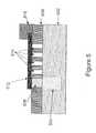
- FIG. 5illustrates an exemplary structure 500 utilizing heat transfer fabric portions that are suspended over air/vacuum gaps.
- Structure 500includes a substrate 502 , an active region 504 , a low thermal conductivity layer 506 , a moderate to high thermal conductivity region 508 , air gaps 510 , a suspended nanotube fabric 512 and a thermal reservoir 516 .
- Gaps 510are defined by supports in low thermal conductivity layer 506 , beneath the nanotube fabric 512 .
- Fabric 512is in thermal contact with active region 504 via moderate to high thermal conductivity region 508 , and with thermal reservoir region 516 . In operation, heat flows from active region 504 , through moderate to high thermal conductivity region 508 , through nanotube fabric 512 , and into reservoir 516 .
- CNT fabricscan be applied to an entire wafer, patterned, and selected sections can be removed.
- heat-transfer sectionscan be left in desired locations to remove heat from selected sites. Therefore, any location on the chip that is highly sensitive to heat loads can have a patterned CNT heat transfer fabric applied adjacent to it in order to remove the excess heat load. Because the entire wafer surface may be covered with CNT fabric and selected portions of fabric can be removed (or even used as other electronic elements as described above), large arrays of CNT heat pipes can be fabricated in parallel.
- the lithography technology node usedgenerally dictates minimum array spacing and size array size.
- FIG. 6is a plan view of an exemplary heat transfer fabric that has been patterned to remove heat from many selected heat sensitive sites on a wafer substrate.
- Structure 600has a substrate 602 , heat sensitive active regions 604 , patterned CNT heat transfer fabric regions 606 , non-heat sensitive active regions 608 and a thermal reservoir 610 .
- Heat transfer fabric regions 606are each in thermal contact with a corresponding heat sensitive active region 604 , and with thermal reservoir 610 . In operation, heat flows from active regions 604 , through patterned CNT heat transfer fabric regions 606 , and into reservoir 610 .
- the substrate 602is created and heat sensitive active regions 604 , non-heat sensitive active regions 608 and a thermal reservoir 610 may be deposited on or created on the substrate 602 .
- a carbon nanotube based fabricis then created, e.g. by spin coating or by aerosol application or dipping.
- the fabricis then patterned, and selected regions of the fabric are removed to create patterned CNT heat transfer fabric regions 606 .
- Nanotube fabric fabrication, patterning, and removal techniquesmay be found in the incorporated patent references.
- FIG. 7illustrates a prior art structure used for the removal of heat from an encapsulated chip.
- Structure 700includes an encapsulation material 702 , terminals 704 , contacts 706 , a semiconductor chip 708 , and a heat sink 710 .
- encapsulation material 702includes an encapsulation material 702 , terminals 704 , contacts 706 , a semiconductor chip 708 , and a heat sink 710 .
- thermal greaseor another thermally conductive material is used to conduct heat between the encapsulated semiconductor chip 708 and the heat sink 710 .
- nanotube fabricse.g., multilayered (e.g., 10-500 nm) nanotube fabrics can be used to transfer the heat from heat sensitive encapsulated areas on an electronic chip.
- Multilayered nanotube fabricscan be formed, e.g., by employing a spray coating process, or with other methods such as those described in the incorporated patent references.
- FIGS. 8A and 8BTwo exemplary architectures for using a nanotube fabric to transfer heat from an encapsulated chip, e.g., an IC, are illustrated in FIGS. 8A and 8B .
- FIG. 8Aillustrates a structure 800 which includes encapsulation material 802 , terminals 804 , contacts 806 , a semiconductor chip 808 , a heat sink 810 , and a heat-conducting layer of nanotubes 812 .
- the heat-conducting layer of nanotubes 812is disposed between the semiconductor chip 808 and the heat sink 810 so that it can carry heat from the chip to the heat sink.
- FIG. 8Billustrates another exemplary heat transfer structure 850 .
- Structure 850has encapsulation material 802 , terminals 804 , contacts 806 , a semiconductor chip 808 , a thermal reservoir 852 , (a metal cover may be used as a thermal reservoir, for example), and a heat-conducting layer of nanotubes 854 ; the layer of nanotube fabric may include a supporting layer.
- the supporting layeris used to support the CNT fabric until it reaches the thermal sink.
- the substrate(not shown in the schematic) is typically not important to the design and operation of the chip.) Note that the nanotube fabric layer in the embodiment shown in FIG. 8B has a non-planar configuration.
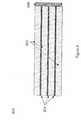
- FIG. 9illustrates a structure 900 that includes stacked chips (wafers) 902 , heat transfer fabric layers 904 and a thermal reservoir 906 .
- the fabric layers 904are disposed between, and preferably in thermal contact with, overlying and underlying (where applicable) stacked chips 902 .
- the stacked chips 902are shown in contact with a thermal reservoir 906 , however the chips 902 need not be in such contact.
- the fabric heat transfer layers 904are in thermal contact with the thermal reservoir 906 , and conduct heat from the stack of wafers into the thermal reservoir 906 .
- the CNT fabricWhen the heat transfer fabric is used with 3-D stacked wafers, the CNT fabric may be deposited in-between the wafers for example by spin-coating or spray-coating. The CNT fabric will then transfer any excess heat away from the mid-regions of the stack to an external thermal reservoir.
- the use of CNTsis advantageous over other thermal management technologies such as Cu in that the CNTs typically do not react with the surrounding substrates and therefore will not contaminate the sensitive electronics, are easily deposited, and have adjustable thickness that can be quite thin, e.g., a few nanometers.
- the heat conduction properties of the nanotube fabricsmay be altered by tailoring the composition, size, shape, and/or geometry of the CNT fabric. For example, thicker and denser fabrics will generally conduct more total heat than sparser fabrics, and wider fabrics will generally conduct more heat than narrower fabrics of the same density. Three-dimensional parameters of the fabrics may affect their thermal transport properties as well. The materials that contact the nanotube fabrics will also have an effect on heat transfer and/or dissipation. The heat conduction properties are also controllable and therefore tailorable by altering the composition of the nanotubes (i.e. SWNTs and MWNTs), etc. The heat conduction properties of individual CNTs can be altered by functionalization, e.g., to restrict or enhance the transport of heat from the thermal load.
- the fabricsmay be composed of all multi-walled nanotubes or of a combination of single- and multi-walled nanotubes.
- nanotube-based heat transfer elementsuse traces of electrically conductive articles made from nanotube layers 106 , such as those shown in FIGS. 1 and 2 .
- the layersmay have a minimum thickness of about 10 nm or less, i.e., the thickness of a given nanotube, and a typical thickness of about 50 nm. Thicknesses greater than 50 nm are useful and the thickness is determined based on the end use of the given transfer fabric.
- the fabricsmay be patterned to a minimum dimension of 150 nm with a maximum width of several microns. The wider fabrics will give a higher heat transfer rate due to the expected higher thermal conductivity of the redundant tubes. Another important parameter includes the number of nanotubes in the fabric.
- the thermal transfer lengthis also important. Minimum lengths of several hundred nanometers may provide superior heat transfer properties, while the thermal conductivity of the system may be expected to decrease with lengths up to several microns, due to serial connection of nanotubes, causing perturbations in the transport of heat. Heat transfer may depend on the thickness of the nanotube fabric as well, with thicknesses in the range of 10-100 nm being envisioned for various applications.
- the nanotube matteis grown or deposited on a surface, such as that of a silicon wafer, to form a contiguous film of a given density.
- the same two dimensional film that may be patterned into discrete heat transfer elementscan also be patterned to generate conductively interconnecting traces ranging in width from 1 nm (the intrinsic minimum size of a nanotube) to hundreds of microns or greater, depending on the application and context, as well as other electronic elements as described in incorporated references, including, but not limited to: transistors, triodes and memory elements.
- Heat transfer elementsmay be formed from a single layer of conducting nanotube fabric where certain portions of the fabric are caused to become insulating while leaving other portions conductive. Further details on patterning dielectric features into nanotube fabrics may be found in U.S. patent application Ser. No. 11/398,126.
Landscapes
- Engineering & Computer Science (AREA)
- Computer Hardware Design (AREA)
- Power Engineering (AREA)
- Microelectronics & Electronic Packaging (AREA)
- Physics & Mathematics (AREA)
- General Physics & Mathematics (AREA)
- Condensed Matter Physics & Semiconductors (AREA)
- Chemical & Material Sciences (AREA)
- Materials Engineering (AREA)
- Carbon And Carbon Compounds (AREA)
- Cooling Or The Like Of Semiconductors Or Solid State Devices (AREA)
- Semiconductor Memories (AREA)
- Non-Volatile Memory (AREA)
Abstract
Description
- This application claims the benefit under 35 U.S.C. §119(e) of U.S. Provisional Patent Application No. 60/714,386, filed Sep. 6, 2005 and entitled “Carbon Nanotubes for the Selective Transfer of Heat from Electronics,” the entire contents of which are incorporated herein by reference.
- 1. Technical Field
- The present application relates generally to nanotube fabrics and methods of making same.
- 2. Discussion of Related Art
- As ultra-large-scale-integration of integrated circuits, microelectronic components and devices are becoming increasingly more dense and compact, there exists an increasing need for smaller and more potent heat transfer devices due to the excessive on-chip heat generation. Current integrated circuits used in microprocessors operated at high frequencies use power densities on the order of 50 W/cm2: in comparison, a 60 W light bulb generates 0.5 W/cm2. Such power densities lead to highly localized heating of integrated circuits in areas known as “hot spots”.
- As the rise in power density increases, the number of “hot spots” on the surface of high power chips increases as observed in microprocessors. Cooling microprocessors is generally necessary to prevent device degradation and to achieve the best possible device performance. A maximum safe temperature for integrated circuit (IC) operation is typically between 100-120° C.
- Solving the problems that “hot spots” present is imperative for the next-generation IC packages, as there is an ever-increasing need for smaller-scale devices. Carbon nanotubes (CNTs) are being used in many different applications in the field of electronics and are found to be extremely useful due to their electrical, mechanical, optical, chemical and thermal properties.
- Carbon nanotubes, with tube diameters around 1-2 nm, are electrical conductors that are able to carry extremely high current densities. They also have the highest known thermal conductivity, and are also generally thermally and chemically stable. Further details on characteristics of carbon nanotubes may be found in the following references, the entire contents of which are incorporated herein by reference: Z. Yao, C. L. Kane, C. Dekker, Phys. Rev. Lett. 84, 2941 (2000); P. M. Ajayan, T. W. Ebbesen, Rep. Prog. Phys. 60, 1025 (1997); Savas Berber, Young-Kyun Kwon and David Tománek, “Unusually High Thermal Conductivity of Carbon Nanotubes,” Phys. Rev. Lett. 84(20), 4613-4616 (2000); Jianwei Che, Tahir Cagin and William A Goddard III, “Thermal conductivity of carbon nanotubes,” Nanotechnology, 11, 65-69, 2000; J. Hone, M. Whitney and A Zettl, “Thermal conductivity of single-walled carbon nanotubes,” Synthetic Metals, 103-2498-2499, 1999 and Mohamed A Osman and Deepak Srivastava, “Temperature dependence of the thermal conductivity of single-wall carbon nanotubes,” Nanotechnology, 12, 21-24, 2001.
- Using individual nanotubes for heat transfer, however, can be problematic because of difficulties in growing them with suitably controlled orientation, length, and the like.
- There is a need in the art for very efficient, very small, even submicron-sized, heat transfer elements which are easily fabricated and are compatible with electronics applications and fabrication techniques. There is likewise a need in the art for large scale fabrication methods of heat transfer devices used for electronic applications in the semiconductor industry which can be monolithically integrated into a CMOS or similar process flow to fabricate integrated circuits. Naturally, the uses of such elements extend to most types of consumer electronics where heat transfer in integrated elements is beneficial.
- The present invention provides carbon nanotubes for the selective transfer of heat from electronics.
- Under one aspect, a method of cooling a circuit element includes providing a thermal reservoir having a temperature lower than an operating temperature of the circuit element; and providing a nanotube article in thermal contact with the circuit element and with the reservoir, the nanotube article including a non-woven fabric of nanotubes in contact with other nanotubes to define a plurality of thermal pathways along the article, the nanotube article having a nanotube density and a shape selected such that the nanotube article is capable of transferring heat from the circuit element to the thermal reservoir.
- One or more embodiments include one or more of the following features. Providing the nanotube article includes depositing pre-formed nanotubes on a surface so as to form the non-woven fabric of nanotubes. Depositing pre-formed nanotubes includes at least one of spin-coating pre-formed nanotubes and spray-coating pre-formed nanotubes. Providing the nanotube article includes growing nanotubes on a surface so as to form the non-woven fabric of nanotubes.
- Further including defining the shape of the nanotube article lithographically. Defining the shape of the nanotube article lithographically includes forming a non-woven fabric of nanotubes and subsequently removing selected portions of that non-woven fabric of nanotubes in accordance with the shape. Providing the nanotube article includes conformally forming a non-woven nanotube fabric over the circuit element. The nanotube article has a substantially planar shape. Further including providing a substrate having a substantially planar major surface and a feature not in the plane of the major surface, and wherein the nanotube article substantially conforms to said feature. Further including providing supports under the nanotube article, the supports defining a gap over which the nanotube article is suspended. The nanotube density and shape are selected such that the nanotube article is capable of transferring heat from the circuit element to the thermal reservoir at a pre-defined rate selected to maintain the circuit element below a pre-specified temperature. The pre-specified temperature includes an upper limit of a normal operating temperature. The nanotube article further has a pre-defined composition. The pre-defined composition includes single-walled nanotubes. The pre-defined composition includes multi-walled nanotubes. The circuit element includes at least a portion of an integrated circuit. The circuit element includes an encapsulation material. The thermal reservoir includes a heat sink. The heat sink includes a plurality of fins that radiate heat. Further including a thermally conductive material between and in thermal contact with each of the nanotube article and the circuit element.
- Under another aspect, a method of forming a thermal management structure for an integrated circuit includes depositing a layer of pre-formed nanotubes on a defined region of the integrated circuit, the layer substantially conforming to the defined region of the integrated circuit and including a plurality of nanotubes; and providing a thermal reservoir in thermal contact with at least a portion of the layer of nanotubes, wherein the layer of pre-formed nanotubes has a nanotube density selected such that the nanotube article is capable of transferring heat from the integrated circuit to the thermal reservoir.
- One or more embodiments includes one or more of the following features. Depositing the layer of pre-formed nanotubes includes at least one of spin-coating and spray-coating pre-formed nanotubes onto the defined region of the integrated circuit. Further including patterning the layer of pre-formed nanotubes to provide defined regions of nanotubes over pre-selected portions of the integrated circuit. The defined regions of nanotubes are each in thermal contact with the thermal reservoir. The pre-selected portions of the integrated circuit include portions of the circuit needing cooling during operation. The pre-selected portions of the integrated circuit include individual devices within the integrated circuit. The pre-selected portions of the integrated circuit include active regions of the integrated circuit. The layer of pre-formed nanotubes includes providing a patterned mask over the layer of pre-formed nanotubes and removing a portion of the layer of pre-formed nanotubes in accordance with the patterned mask. Patterning the layer of pre-formed nanotubes further includes defining at least one of a memory element, a heat emitter, a channel in a field effect transistor, a gate in a field effect transistor, a relay, a conductor, and a sensor within the layer of pre-formed nanotubes. Further including patterning the layer of pre-formed nanotubes to define regions of modified thermal conductivity. Further including functionalizing at least a portion of the nanotubes of the layer of pre-formed nanotubes. The integrated circuit is substantially encapsulated. The integrated circuit is substantially complete before depositing the nanotube layer thereon. Further including providing a second integrated circuit over the previously mentioned integrated circuit with the layer of pre-formed nanotubes there between, the layer of pre-formed nanotubes being in thermal contact with the second integrated circuit. The nanotubes of the layer of pre-formed nanotubes includes define a plurality of thermal pathways within the layer of pre-formed nanotubes. The layer of pre-formed nanotubes includes a non-woven fabric of entangled nanotubes. At least some of the nanotubes of the layer of pre-formed nanotubes have a length of at least 100 nm. The layer of pre-formed nanotubes has a thickness between about 1 nm and about 100 nm. The layer of pre-formed nanotubes is substantially a monolayer of nanotubes. The defined region of the integrated circuit includes the top surface of the integrated circuit.
FIG. 1 illustrates an embodiment of a lateral heat transfer structure;FIGS. 2A and B are micrographs of nanotube fabrics and patterning thereof;FIG. 3 illustrates an embodiment of a vertical heat transfer structure;FIGS. 4A-4C are micrographs of conformal nanotube fabrics;FIG. 5 illustrates an embodiment of a partially suspended heat transfer structure;FIG. 6 illustrates an embodiment of an array heat transfer structure;FIG. 7 illustrates a conventional heat sink on an integrated circuit;FIGS. 8A and 8B illustrate embodiments of heat transfer structures used to transfer heat from an integrated circuit; andFIG. 9 illustrates an embodiment of a heat transfer structure used to transfer heat from a stack of wafers.- Non-woven fabrics of carbon nanotubes (CNTs) can help manage the problem of thermal “hot spots” and heat transfer in high power devices. CNT fabrics have superior thermal conductance relative to single nanotube as well as to conventional conductive materials such as metals, and therefore the CNT fabrics have a tremendous potential for providing extremely efficient heat transfer. CNTs exhibit a very high “axial” thermal conductivity. For a discrete multiwalled nanotube (MWNT), the thermal conductivity is expected to surpass 3000 W/m-k along the tube axis, while theoretical studies of single walled nanotubes (SWNTs) have shown that thermal conductivities of 6600 W/m-K are possible. CNT fabrics can be used as effective heat-sinks, which are able to remove large amounts of heat away from critical “hot spots”.
- Preferred embodiments of this invention use CNT fabrics for the transfer of heat away from heat sensitive areas in an electronic circuit or from an entire electronic chip. Similar to other carbon allotropes, CNTs have a high thermal conductivity, where thermal conductivity is defined as the ability of a material to remove heat by a relationship between the negative temperature gradient and the ratio of the heat flow rate per unit area. Thermal conductivity is defined by the equation
- where κ is the thermal conductivity of the material, Q is the quantity of heat in Joules, t is time in seconds, A is area-m2, temperature (T) is measured in degrees K, and x is measured in meters. The thermal conductivity of a material is dictated by electronic and/or phonon propagation and the thermal conductivity of materials will add in parallel; therefore, for multiple metal lines in parallel, the heat transfer rate can be calculated by using equation:
- Unlike the other forms of carbon, the thermal conductivity of nanotubes is confined along the axis of the nanotube due to its 1-D structure. The thermal conductivity of CNTs is theoretically predicted to be greater than about 2000 W/m-K, with values of 6600 W/m-K possible, while experimental measurements have demonstrated thermal conductivity of greater than about 200 W/m-K at room temperature comparable to bulk Cu (about 400 W/m-K) and bulk Al (about 300 W/m-K) at room temperature. The disparity between theoretical and experimental results is typically attributed to deformations along the structure of the CNTs and the effects of non-ideal contacts and test set-up for the measuring of thermal conductivity. Unlike high thermal conductivity metals, CNTs are easily deposited and patterned to nanometer dimensions, the thermal conductivity of the nanotubes do not decrease with increased temperature (typically up to about 500 K) and CNTs have a high melting point (typically over about 3000 K). SWNTs also typically possess the ability to carry a high current density (e.g., over about 109A/cm2) and the nanotubes do not readily react/diffuse with their surroundings, unlike conventional highly thermally conductive materials such as metals. The combination of these unique properties makes CNT fabrics useful for the thermal management of heat sensitive areas on a semiconductor chip, 3-D stacked wafers and other applications where removal of heat is required.
- CNT fabrics have several features that can be useful for heat transfer and are not generally available with conventional heat transfer technologies. First, the very layer of fabric used to make the heat transfer element can also be used to make other electronic elements on the same substrate. For example, a single CNT fabric can be patterned to produce different regions that may be utilized, e.g., as heat transfer media, memory elements, heat emitters, channels or gates in field effect transistors, relays, conductors, electrical insulators, and/or sensors, or a plethora of other types of elements depending on how the sections of the fabric are patterned and processed. Examples of nanotube fabric devices and methods of making same may be found in the incorporated patent references, given below. Second, VLSI arrays of these CNT heat transfer fabrics can be formed using patterning technology at minimum dimensions of the lithography node used, e.g., giga-sized CNT heat emitter arrays can be fabricated at 180 nm or smaller critical feature size. Such methods are more fully described in the incorporated patent references. Third, such nanofabric-based heat transfer fabrics devices scale directly with the lithographic ground rule used, such that, e.g., 180 nm, 130 nm, 90 nm and 65 nm sized emitters can be produced.
- Under certain embodiments of the invention, the heat transfer articles may be made from a nanotube non-woven fabric, layer or film, typically of entangled or matted nanotubes, which in some cases may be patterned into ribbons or belts. Creating ribbons or belts (more generally referred to as “traces”) of patterned nanotube fabrics overcomes many of the difficulties that may arise in attempting to grow “aligned” CNTs with controlled orientation, length, and the like. Creating traces from nanotube fabrics allows the traces to retain many if not all of the benefits of individual nanotubes. Moreover, traces made from nanotube fabric have benefits not found in individual nanotubes. For example, since the traces include many nanotubes in aggregation, the traces will generally not fail as the result of a failure or break of an individual nanotube. Instead, there are many alternate paths through which heat (e.g., phonons) may travel within a given trace. In effect, a trace made from nanotube fabric defines a heat transfer network of individual nanotubes, each of which conducts heat. Moreover, by using nanotube fabrics, layers or films, current technology may be used to create such traces.
- The nanotube fabric may be disposed on the substrate and may be created by spin coating, spray coating, direct growth, or any other appropriate method. After the CNT fabric is deposited, the fabric can be patterned to make heat transfer ribbons, e.g., using standard CMOS lithographic and etching processes. For example,
FIG. 2 shows a CNT fabric that has been patterned to have nanometer sized dimensions, here a 250 nm wide CNT pattern (more on this below). Unlike more conventional techniques which typically rely on directed growth or chemical self-assembly of individual nanotubes, preferred embodiments utilize fabrication techniques involving thin films and in most cases, lithography, which allow fabrication over large surface—i.e. >6″ silicon based substrates used for electronic circuits. (In contrast, growing individual nanotubes over a distance beyond sub millimeter distances is typically unfeasible.) Exemplary methods of making and patterning nanotube fabrics may be found in the incorporated patent references. - Once the CNT fabric has been patterned, further processing can then be performed, typically without damaging the properties and characteristics of the patterned CNT fabric. For example, the CNT fabric can be exposed to various metal deposition methods, various etching methods and various corrosive and reductive atmospheres, generally without any degradation of the CNT fabric's properties.
- CNT fabrics are generally easily manufactured and fabricated using standard front-end and back-end CMOS integration equipment and techniques. Highly conductive metals such as copper, on the other hand, require electro-deposition and Chemical-Mechanical-Planarization (CMP) techniques to create damascene structures to use on the chip; such techniques require large areas of chips. CNTs do not typically require large amounts of surface space and may be easily patterned, e.g., with oxygen plasmas. The thermal conductivity of copper generally decreases with shrinking feature size. In contrast, as the size of CNT fabric-based heat transfer devices decrease, the number of conductive tubes decreases, so the overall thermal conductance (generally the thermal conductivity times cross-sectional area divided by length) decreases, however the individual CNT thermal conductivity remains the same.
- The thermal conductivity of a monolayer fabric is generally greater than that of a single carbon nanotube due to the additive effects of the multiple heat conducting tubes. The thermal conductivity of a monolayer fabric is also generally greater than a layer of copper with the same geometry, due to the greater thermal conductivity per cross sectional area of carbon nanotubes as compared to copper. CNTs also do not typically interact with surrounding materials, as copper does. For example, CNTs will not generally diffuse through various material layers and alter/destroy active regions of electronic devices (i.e. the active conductive channel of Si MOS devices), therefore, there is no need to take precautions against this when using CNTs as would be necessary when using copper (which is a deep level trap for silicon).
- The ability to deposit and pattern the CNT fabric allows for the creation of CNT heat pipes/channels on-chip that can transfer large amounts of thermal power away from sensitive active regions on semiconductor electronics.
FIG. 3 illustrates a cross section of an exemplary device. - An embodiment of a simple
heat transfer structure 100 is illustrated inFIG. 1 .Structure 100 includes asubstrate 102, aheat load 104, aheat transfer fabric 106 and aheat reservoir 108.Fabric 106 is in thermal contact withheat load 104 and withheat reservoir 108, and transfers heat fromheat load 104 to heatreservoir 108. This structure is shown only as an example, any architecture may be used in which the geometry is arranged so that the nanotube fabric can transfer heat from a (hotter) thermal load to a (cooler) thermal reservoir, and the nanotube fabric has a size, shape, and nanotube density (e.g., thickness) selected to transfer a sufficient amount of heat from the thermal load to the thermal reservoir. For example, a fabric used to cool a conventional integrated circuit would generally have a size and shape sufficient to cover the parts of the integrated circuit that need cooling, and the fabric would have enough nanotubes (of the correct type) to transfer heat from the integrated circuit to a thermal reservoir at a rate sufficient that the integrated circuit would remain at a safe operating temperature, e.g., 100-120° C. - In some embodiments a nanotube fabric is fabricated over an entire wafer surface, and then portions of the fabric are removed by patterning, thereby leaving heat-transferring portions only in desired locations. Such patterning may be accomplished by using methods such as those in the incorporated patent references.
FIG. 2A illustrates patternedphotoresist 202 disposed on a section ofnanotube fabric 204 overlying asubstrate 206. According to one method of nanotube patterning, the exposedfabric 204 and the resist202 are exposed to an ashing procedure thereby removing the exposed nanotube fabric. The resist202 is subsequently removed, and the patternedfabric 208 remains, as shown inFIG. 2B .FIG. 2B illustrates a patterned, relativelysparse nanotube fabric 208. In a configuration such as that shown inFIG. 1 , such a fabric is capable of conducting heat away from a “hot spot” such asheat load 104, to a thermal reservoir (in some cases referred to as a “heat sink,” such asthermal reservoir 106. - A second
exemplary device 300 that could be used for on-chip thermal management of high heat load active regions is illustrated inFIG. 3 .Device 300 has a high heat loadactive region 302, a low-thermal conductivity region304 (such as silicon or silicon dioxide), a moderate to high thermal conductivity region306 (such as an interconnect metallization layer), ananotube fabric 308 and athermal reservoir region 310.Fabric 308 is in thermal contact with heat loadactive region 302 via moderate to highthermal conductivity region 306, and withthermal reservoir region 310. In operation, heat flows fromheat load 302, through moderate to highthermal conductivity region 306, throughnanotube fabric 308, and intoreservoir 310. The geometry and exact relative placement of the elements ofstructure 300 need not be as described; one skilled in the art will understand that as long as the geometry and composition offabric 308 is configured to lead heat away from the heat loadactive region 302 then the thermal transfer properties of thefabric 308 may be utilized. - Nanotube fabrics and ribbons thereof have also been shown to substantially conform to a surface, such as a surface of an article on a semiconductor substrate. For example, the fabric is generally horizontally oriented when the surface of the substrate that receives the fabric is horizontally oriented, and the fabric is generally vertically oriented on a vertical surface of a suitable substrate. Fabrication techniques to develop such horizontally- and vertically-disposed fabrics and devices using such nanotube fabrics, may be created via CVD or by room temperature operations; further details may be found in the incorporated patent references. This feature allows nanotube fabrics to be used as heat transfer media on a wide variety of semiconductor substrates and features.
FIGS. 4A-4C illustrate typical conformal properties of carbon nanotube fabrics.FIG. 4A is a micrograph of apatterned nanotube fabric 400 disposed upon a substrate402 with raised features404.FIGS. 4B and 4C are detailed micrographs of ananotube fabric 400 conforming to a substantiallyvertical substrate feature 404. - CNT fabrics can also be suspended by supports above the surface of the substrate. Suspending heat transfer fabrics can enhance the ability of the fabrics to conduct heat while not being significantly influenced by the surrounding/underlying substrate since the suspension of the fabric will prevent any interaction between the substrate and the CNTs that may perturb the transfer of heat along the axis of the CNTs due to deformation caused in the tube because of the van der Waals forces present on the surface. Suspending the CNT fabric may also reduce or eliminate the possibility of the large surface area of the substrate retaining heat, which may prevent the CNT fabric from adequately transferring the heat away from the active device.
FIG. 5 illustrates an exemplary structure500 utilizing heat transfer fabric portions that are suspended over air/vacuum gaps. Structure500 includes asubstrate 502, anactive region 504, a lowthermal conductivity layer 506, a moderate to highthermal conductivity region 508,air gaps 510, a suspendednanotube fabric 512 and athermal reservoir 516.Gaps 510 are defined by supports in lowthermal conductivity layer 506, beneath thenanotube fabric 512.Fabric 512 is in thermal contact withactive region 504 via moderate to highthermal conductivity region 508, and withthermal reservoir region 516. In operation, heat flows fromactive region 504, through moderate to highthermal conductivity region 508, throughnanotube fabric 512, and intoreservoir 516.- As mentioned above, CNT fabrics can be applied to an entire wafer, patterned, and selected sections can be removed. Thus, heat-transfer sections can be left in desired locations to remove heat from selected sites. Therefore, any location on the chip that is highly sensitive to heat loads can have a patterned CNT heat transfer fabric applied adjacent to it in order to remove the excess heat load. Because the entire wafer surface may be covered with CNT fabric and selected portions of fabric can be removed (or even used as other electronic elements as described above), large arrays of CNT heat pipes can be fabricated in parallel. The lithography technology node used generally dictates minimum array spacing and size array size.
FIG. 6 is a plan view of an exemplary heat transfer fabric that has been patterned to remove heat from many selected heat sensitive sites on a wafer substrate.Structure 600 has asubstrate 602, heat sensitiveactive regions 604, patterned CNT heattransfer fabric regions 606, non-heat sensitiveactive regions 608 and athermal reservoir 610. Heattransfer fabric regions 606 are each in thermal contact with a corresponding heat sensitiveactive region 604, and withthermal reservoir 610. In operation, heat flows fromactive regions 604, through patterned CNT heattransfer fabric regions 606, and intoreservoir 610.- The
substrate 602 is created and heat sensitiveactive regions 604, non-heat sensitiveactive regions 608 and athermal reservoir 610 may be deposited on or created on thesubstrate 602. A carbon nanotube based fabric is then created, e.g. by spin coating or by aerosol application or dipping. The fabric is then patterned, and selected regions of the fabric are removed to create patterned CNT heattransfer fabric regions 606. Nanotube fabric fabrication, patterning, and removal techniques may be found in the incorporated patent references. - CNT fabrics can also be employed to transfer heat from entire chips to external heat reservoirs.
FIG. 7 illustrates a prior art structure used for the removal of heat from an encapsulated chip.Structure 700 includes anencapsulation material 702,terminals 704,contacts 706, asemiconductor chip 708, and aheat sink 710. Typically, “thermal grease” or another thermally conductive material is used to conduct heat between the encapsulatedsemiconductor chip 708 and theheat sink 710. - According to certain embodiments, nanotube fabrics, e.g., multilayered (e.g., 10-500 nm) nanotube fabrics can be used to transfer the heat from heat sensitive encapsulated areas on an electronic chip. Multilayered nanotube fabrics can be formed, e.g., by employing a spray coating process, or with other methods such as those described in the incorporated patent references. Two exemplary architectures for using a nanotube fabric to transfer heat from an encapsulated chip, e.g., an IC, are illustrated in
FIGS. 8A and 8B . FIG. 8A illustrates astructure 800 which includesencapsulation material 802,terminals 804,contacts 806, asemiconductor chip 808, aheat sink 810, and a heat-conducting layer ofnanotubes 812. The heat-conducting layer ofnanotubes 812 is disposed between thesemiconductor chip 808 and theheat sink 810 so that it can carry heat from the chip to the heat sink.FIG. 8B illustrates another exemplaryheat transfer structure 850.Structure 850 hasencapsulation material 802,terminals 804,contacts 806, asemiconductor chip 808, athermal reservoir 852, (a metal cover may be used as a thermal reservoir, for example), and a heat-conducting layer ofnanotubes 854; the layer of nanotube fabric may include a supporting layer. (The supporting layer is used to support the CNT fabric until it reaches the thermal sink. The substrate (not shown in the schematic) is typically not important to the design and operation of the chip.) Note that the nanotube fabric layer in the embodiment shown inFIG. 8B has a non-planar configuration.- Nanotube fabrics can also be used to remove heat from 3-D stacked wafers.
FIG. 9 illustrates astructure 900 that includes stacked chips (wafers)902, heat transfer fabric layers904 and athermal reservoir 906. As can be seen inFIG. 9 , the fabric layers904 are disposed between, and preferably in thermal contact with, overlying and underlying (where applicable)stacked chips 902. Thestacked chips 902 are shown in contact with athermal reservoir 906, however thechips 902 need not be in such contact. The fabric heat transfer layers904 are in thermal contact with thethermal reservoir 906, and conduct heat from the stack of wafers into thethermal reservoir 906. - When the heat transfer fabric is used with 3-D stacked wafers, the CNT fabric may be deposited in-between the wafers for example by spin-coating or spray-coating. The CNT fabric will then transfer any excess heat away from the mid-regions of the stack to an external thermal reservoir. The use of CNTs is advantageous over other thermal management technologies such as Cu in that the CNTs typically do not react with the surrounding substrates and therefore will not contaminate the sensitive electronics, are easily deposited, and have adjustable thickness that can be quite thin, e.g., a few nanometers.
- The heat conduction properties of the nanotube fabrics may be altered by tailoring the composition, size, shape, and/or geometry of the CNT fabric. For example, thicker and denser fabrics will generally conduct more total heat than sparser fabrics, and wider fabrics will generally conduct more heat than narrower fabrics of the same density. Three-dimensional parameters of the fabrics may affect their thermal transport properties as well. The materials that contact the nanotube fabrics will also have an effect on heat transfer and/or dissipation. The heat conduction properties are also controllable and therefore tailorable by altering the composition of the nanotubes (i.e. SWNTs and MWNTs), etc. The heat conduction properties of individual CNTs can be altered by functionalization, e.g., to restrict or enhance the transport of heat from the thermal load. Investigators have shown that functionalization of single-walled carbon nanotubes drastically reduces their thermal conductivities, see Padgett et al., “Influence of Chemisorption on the Thermal Conductivity of Single-Wall Carbon Nanotubes,” Nano Letters, 4 (6), 1051-1053, 2004, the entire contents of which are incorporated herein by reference. This can be a useful feature in cases where there are some areas on a given wafer that do not require rapid transport of heat away from an active region.
- There are several possible commercial applications for this product. One such application would be to regulate the amount of heat that is stored at selective regions on the chip. A second application involves the removal of large amounts of thermal power from encapsulated chips and a third possible product would involve the removal of heat from 3-D stacked wafers.
- Though most of the disclosure above is written as if the fabric were made of nanotubes of the same type, e.g., all single-walled, the fabrics may be composed of all multi-walled nanotubes or of a combination of single- and multi-walled nanotubes.
- The above-described embodiments of nanotube-based heat transfer elements use traces of electrically conductive articles made from
nanotube layers 106, such as those shown inFIGS. 1 and 2 . The layers may have a minimum thickness of about 10 nm or less, i.e., the thickness of a given nanotube, and a typical thickness of about 50 nm. Thicknesses greater than 50 nm are useful and the thickness is determined based on the end use of the given transfer fabric. The fabrics may be patterned to a minimum dimension of 150 nm with a maximum width of several microns. The wider fabrics will give a higher heat transfer rate due to the expected higher thermal conductivity of the redundant tubes. Another important parameter includes the number of nanotubes in the fabric. Higher nanotube densities will give a higher overall thermal conductivity of the system due to the combined effect of the individual nanotubes. The thermal transfer length is also important. Minimum lengths of several hundred nanometers may provide superior heat transfer properties, while the thermal conductivity of the system may be expected to decrease with lengths up to several microns, due to serial connection of nanotubes, causing perturbations in the transport of heat. Heat transfer may depend on the thickness of the nanotube fabric as well, with thicknesses in the range of 10-100 nm being envisioned for various applications. The nanotube matte is grown or deposited on a surface, such as that of a silicon wafer, to form a contiguous film of a given density. The same two dimensional film that may be patterned into discrete heat transfer elements can also be patterned to generate conductively interconnecting traces ranging in width from 1 nm (the intrinsic minimum size of a nanotube) to hundreds of microns or greater, depending on the application and context, as well as other electronic elements as described in incorporated references, including, but not limited to: transistors, triodes and memory elements. - Heat Transfer Elements with Dielectric Patterning
- Heat transfer elements may be formed from a single layer of conducting nanotube fabric where certain portions of the fabric are caused to become insulating while leaving other portions conductive. Further details on patterning dielectric features into nanotube fabrics may be found in U.S. patent application Ser. No. 11/398,126.
- The following commonly-owned patent references, referred to herein as “incorporated patent references,” describe various techniques for creating nanotube elements (nanotube fabric articles and switches), e.g., creating and patterning nanotube fabrics, and are incorporated herein by reference in their entireties:
- U.S. patent application Ser. No. 09/915,093, Electromechanical Memory Array Using Nanotube Ribbons and Method for Making Same, filed Jul. 25, 2001, now U.S. Pat. No. 6,919,592;
- U.S. patent application Ser. No. 09/915,173, Electromechanical Memory Having Cell Selection Circuitry Constructed with Nanotube Technology, filed Jul. 25, 2001, now U.S. Pat. No. 6,643,165;
- U.S. patent application Ser. No. 09/915,095, Hybrid Circuit Having Nanotube Electromechanical Memory, filed Jul. 25, 2001, now U.S. Pat. No. 6,574,130;
- U.S. patent application Ser. No. 10/033,323, Electromechanical Three-Trace Junction Devices, filed Dec. 28, 2001 now U.S. Pat. No. 6,911,682;
- U.S. patent application Ser. No. 10/802,900, Electromechanical Three-Trace Junction Devices, filed Mar. 17, 2004;
- U.S. patent application Ser. No. 10/033,032, Methods of Making Electromechanical Three-Trace Junction Devices, filed Dec. 28, 2001, now U.S. Pat. No. 6,784,028;
- U.S. patent application Ser. No. 10/128,118, Nanotube Films and Articles, filed Apr. 23, 2002, now U.S. Pat. No. 6,706,402;
- U.S. patent application Ser. No. 10/128,117, Methods of Nanotube Films and Articles, filed Apr. 23, 2002 now U.S. Pat. No. 6,835,591;
- U.S. patent application Ser. No. 10/864,186, Non-Volatile Electromechanical Field Effect Devices and Circuits Using Same and Methods of Forming Same, filed Jun. 9, 2004, now U.S. Patent Publication No. 2005/0062035;
- U.S. patent application Ser. No. 10/341,005, Methods of Making Carbon Nanotube Films, Layers, Fabrics, Ribbons, Elements and Articles, filed Jan. 13, 2003;
- U.S. patent application Ser. No. 10/341,055, Methods of Using Thin Metal Layers To Make Carbon Nanotube Films, Layers, Fabrics, Ribbons, Elements and Articles, filed Jan. 13, 2003;
- U.S. patent application Ser. No. 10/341,054, Methods of Using Preformed Nanotube Films, Layers, Fabrics, Ribbons, Elements and Articles, filed Jan. 13, 2003;
- U.S. patent application Ser. No. 10/341,130, Carbon Nanotube Films, Layers, Fabrics, Ribbons, Elements and Articles, filed Jan. 13, 2003;
- U.S. patent application Ser. No. 10/776,059, Electromechanical Switches and Memory Cells Using Horizontally-Disposed Nanofabric Articles and Methods of Making Same, filed Feb. 11, 2004;
- U.S. patent application Ser. No. 10/776,572, Electromechanical Switches and Memory Cells Using Vertically-Disposed Nanofabric Articles and Methods of Making the Same, filed Feb. 11, 2004 now U.S. Pat. No. 6,924,538;
- U.S. patent application Ser. No. 10/917,794, Nanotube-Based Switching Element, filed Aug. 13, 2004;
- U.S. patent application Ser. No. 10/918,085, Nanotube-Based Switching Elements With Multiple Controls, filed Aug. 13, 2004;
- U.S. patent application Ser. No. 10/936,119, Patterned Nanoscopic Articles and Methods of Making the Same, filed Sep. 8, 2004, now U.S. Patent Publication No. 2005/0128788; and
- U.S. patent application Ser. No. 11/398,126, Nanotube Articles with Adjustable Conductivity and Methods of Making the Same, filed Apr. 5, 2006.
- It will be further appreciated that the scope of the present invention is not limited to the above-described embodiments, but rather is defined by the appended claims, and that these claims will encompass modifications of and improvements to what has been described.
Claims (40)
Priority Applications (1)
| Application Number | Priority Date | Filing Date | Title |
|---|---|---|---|
| US12/066,063US7927992B2 (en) | 2005-09-06 | 2006-09-05 | Carbon nanotubes for the selective transfer of heat from electronics |
Applications Claiming Priority (3)
| Application Number | Priority Date | Filing Date | Title |
|---|---|---|---|
| US71438605P | 2005-09-06 | 2005-09-06 | |
| US12/066,063US7927992B2 (en) | 2005-09-06 | 2006-09-05 | Carbon nanotubes for the selective transfer of heat from electronics |
| PCT/US2006/034563WO2008054364A2 (en) | 2005-09-06 | 2006-09-05 | Carbon nanotubes for the selective transfer of heat from electronics |
Related Parent Applications (1)
| Application Number | Title | Priority Date | Filing Date |
|---|---|---|---|
| PCT/US2006/034563A-371-Of-InternationalWO2008054364A2 (en) | 2005-09-06 | 2006-09-05 | Carbon nanotubes for the selective transfer of heat from electronics |
Related Child Applications (1)
| Application Number | Title | Priority Date | Filing Date |
|---|---|---|---|
| US13/090,135ContinuationUS8630091B2 (en) | 2005-09-06 | 2011-04-19 | Carbon nanotubes for the selective transfer of heat from electronics |
Publications (2)
| Publication Number | Publication Date |
|---|---|
| US20100267205A1true US20100267205A1 (en) | 2010-10-21 |
| US7927992B2 US7927992B2 (en) | 2011-04-19 |
Family
ID=39344746
Family Applications (2)
| Application Number | Title | Priority Date | Filing Date |
|---|---|---|---|
| US12/066,063Active2028-05-01US7927992B2 (en) | 2005-09-06 | 2006-09-05 | Carbon nanotubes for the selective transfer of heat from electronics |
| US13/090,135Active2027-11-26US8630091B2 (en) | 2005-09-06 | 2011-04-19 | Carbon nanotubes for the selective transfer of heat from electronics |
Family Applications After (1)
| Application Number | Title | Priority Date | Filing Date |
|---|---|---|---|
| US13/090,135Active2027-11-26US8630091B2 (en) | 2005-09-06 | 2011-04-19 | Carbon nanotubes for the selective transfer of heat from electronics |
Country Status (5)
| Country | Link |
|---|---|
| US (2) | US7927992B2 (en) |
| EP (1) | EP1964188A4 (en) |
| AU (1) | AU2006347609A1 (en) |
| CA (1) | CA2621924A1 (en) |
| WO (1) | WO2008054364A2 (en) |
Cited By (12)
| Publication number | Priority date | Publication date | Assignee | Title |
|---|---|---|---|---|
| US20090032496A1 (en)* | 2007-07-13 | 2009-02-05 | Tsinghua University | Method for manufacturing thermal interface material having carbon nanotubes |
| US20110027497A1 (en)* | 2009-07-31 | 2011-02-03 | Nantero, Inc. | Anisotropic nanotube fabric layers and films and methods of forming same |
| US20110296826A1 (en)* | 2010-06-02 | 2011-12-08 | GM Global Technology Operations LLC | Controlling heat in a system using smart materials |
| US20120312343A1 (en)* | 2011-04-12 | 2012-12-13 | Nanocomp Technologies, Inc. | Nanostructured material based thermoelectric generators and methods of generating power |
| US8574673B2 (en) | 2009-07-31 | 2013-11-05 | Nantero Inc. | Anisotropic nanotube fabric layers and films and methods of forming same |
| US20150223318A1 (en)* | 2014-01-31 | 2015-08-06 | Ibiden Co., Ltd. | Multilayer wiring board |
| US9198232B2 (en) | 2008-05-07 | 2015-11-24 | Nanocomp Technologies, Inc. | Nanostructure-based heating devices and methods of use |
| US9236669B2 (en) | 2007-08-07 | 2016-01-12 | Nanocomp Technologies, Inc. | Electrically and thermally non-metallic conductive nanostructure-based adapters |
| US9422651B2 (en) | 2003-01-13 | 2016-08-23 | Nantero Inc. | Methods for arranging nanoscopic elements within networks, fabrics, and films |
| US9574290B2 (en) | 2003-01-13 | 2017-02-21 | Nantero Inc. | Methods for arranging nanotube elements within nanotube fabrics and films |
| DE102018218832A1 (en)* | 2018-11-05 | 2020-05-07 | Robert Bosch Gmbh | Heat sink with carbon nanostructure-based fibers |
| US11279836B2 (en) | 2017-01-09 | 2022-03-22 | Nanocomp Technologies, Inc. | Intumescent nanostructured materials and methods of manufacturing same |
Families Citing this family (25)
| Publication number | Priority date | Publication date | Assignee | Title |
|---|---|---|---|---|
| EP2860153B1 (en) | 2005-07-28 | 2018-05-16 | Nanocomp Technologies, Inc. | Apparatus and method for formation and collection of nanofibrous non-woven sheet |
| AU2006347609A1 (en) | 2005-09-06 | 2008-05-08 | Nantero, Inc. | Carbon nanotubes for the selective transfer of heat from electronics |
| US8569848B2 (en)* | 2008-07-21 | 2013-10-29 | The Regents Of The University Of California | Nanotube phonon waveguide |
| US9650732B2 (en) | 2013-05-01 | 2017-05-16 | Nantero Inc. | Low defect nanotube application solutions and fabrics and methods for making same |
| US10654718B2 (en) | 2013-09-20 | 2020-05-19 | Nantero, Inc. | Scalable nanotube fabrics and methods for making same |
| US10444799B2 (en)* | 2013-10-30 | 2019-10-15 | Hewlett-Packard Development Company, L.P. | Nanotube coated electronic device housing wall |
| CA3002539A1 (en) | 2015-10-23 | 2017-04-27 | Nanocomp Technologies, Inc. | Directed infrared radiator article |
| EP3206212B1 (en)* | 2016-02-15 | 2022-03-02 | Nokia Technologies Oy | An apparatus and method of forming an apparatus comprising two dimensional material |
| US11332861B2 (en) | 2019-05-16 | 2022-05-17 | Zeon Corporation | Methods for characterizing nanotube formulations for nanotube fabrics with controlled surface roughness and degree of rafting |
| CN113312805B (en)* | 2021-07-29 | 2021-10-26 | 中国人民解放军国防科技大学 | Method for evaluating melting point quality of high-power fiber laser |
| US12191233B2 (en) | 2022-07-28 | 2025-01-07 | Adeia Semiconductor Bonding Technologies Inc. | Embedded cooling systems and methods of manufacturing embedded cooling systems |
| WO2024138186A1 (en) | 2022-12-23 | 2024-06-27 | Adeia Semiconductor Bonding Technologies Inc. | Embedded cooling systems for advanced device packaging |
| KR20250130348A (en) | 2022-12-29 | 2025-09-01 | 아데이아 세미컨덕터 본딩 테크놀로지스 인코포레이티드 | Embedded cooling assembly for advanced device packaging and method for manufacturing the same |
| KR20250130375A (en) | 2022-12-31 | 2025-09-01 | 아데이아 세미컨덕터 본딩 테크놀로지스 인코포레이티드 | Embedded liquid cooling technology |
| US12341083B2 (en) | 2023-02-08 | 2025-06-24 | Adeia Semiconductor Bonding Technologies Inc. | Electronic device cooling structures bonded to semiconductor elements |
| TW202516697A (en) | 2023-03-31 | 2025-04-16 | 美商艾德亞半導體接合科技有限公司 | Integrated cooling assemblies including backside power/ground delivery and methods of manufacturing the same |
| US12191234B2 (en) | 2023-05-17 | 2025-01-07 | Adeia Semiconductor Bonding Technologies Inc. | Integrated cooling assemblies for advanced device packaging and methods of manufacturing the same |
| US20240387323A1 (en) | 2023-05-17 | 2024-11-21 | Adeia Semiconductor Bonding Technologies Inc. | Integrated cooling assemblies including signal redistribution and methods of manufacturing the same |
| US12283490B1 (en) | 2023-12-21 | 2025-04-22 | Adeia Semiconductor Bonding Technologies Inc. | Integrated cooling assemblies for advanced device packaging and methods of manufacturing the same |
| US12368087B2 (en) | 2023-12-26 | 2025-07-22 | Adeia Semiconductor Bonding Technologies Inc. | Embedded cooling systems for advanced device packaging and methods of manufacturing the same |
| US12322677B1 (en) | 2024-02-07 | 2025-06-03 | Adeia Semiconductor Bonding Technologies Inc. | Fluid channel geometry optimizations to improve cooling efficiency |
| US12336141B1 (en) | 2024-03-29 | 2025-06-17 | Adeia Semiconductor Bonding Technologies Inc. | Cold plate cavity designs for improved thermal performance |
| US12176264B1 (en) | 2024-03-29 | 2024-12-24 | Adeia Semiconductor Bonding Technologies Inc. | Manifold designs for embedded liquid cooling in a package |
| US12266545B1 (en) | 2024-05-24 | 2025-04-01 | Adeia Semiconductor Bonding Technologies Inc. | Structures and methods for integrated cold plate in XPUs and memory |
| US12412808B1 (en) | 2024-12-20 | 2025-09-09 | Adeia Semiconductor Bonding Technologies Inc. | Cold plate and manifold integration for high reliability |
Citations (57)
| Publication number | Priority date | Publication date | Assignee | Title |
|---|---|---|---|---|
| US4169911A (en)* | 1977-05-10 | 1979-10-02 | Toray Industries, Inc. | Porous carbon fiber material with a thin metal film covering each fiber |
| US6057637A (en)* | 1996-09-13 | 2000-05-02 | The Regents Of The University Of California | Field emission electron source |
| US20010004979A1 (en)* | 1999-12-14 | 2001-06-28 | Lg Electronics Inc. | Field emission display and method for fabricating the same |
| US6277318B1 (en)* | 1999-08-18 | 2001-08-21 | Agere Systems Guardian Corp. | Method for fabrication of patterned carbon nanotube films |
| US6342276B1 (en)* | 1999-12-10 | 2002-01-29 | Samsung Sdi Co., Ltd. | Method for making a field emission display |
| US6409567B1 (en)* | 1997-12-15 | 2002-06-25 | E.I. Du Pont De Nemours And Company | Past-deposited carbon electron emitters |
| US6423583B1 (en)* | 2001-01-03 | 2002-07-23 | International Business Machines Corporation | Methodology for electrically induced selective breakdown of nanotubes |
| US20020160111A1 (en)* | 2001-04-25 | 2002-10-31 | Yi Sun | Method for fabrication of field emission devices using carbon nanotube film as a cathode |
| US6495116B1 (en)* | 2000-04-10 | 2002-12-17 | Lockheed Martin Corporation | Net shape manufacturing using carbon nanotubes |
| US6495258B1 (en)* | 2000-09-20 | 2002-12-17 | Auburn University | Structures with high number density of carbon nanotubes and 3-dimensional distribution |
| US20030004058A1 (en)* | 2001-05-21 | 2003-01-02 | Trustees Of Boston College | Varied morphology carbon nanotubes and method for their manufacture |
| US6515339B2 (en)* | 2000-07-18 | 2003-02-04 | Lg Electronics Inc. | Method of horizontally growing carbon nanotubes and field effect transistor using the carbon nanotubes grown by the method |
| US6528020B1 (en)* | 1998-08-14 | 2003-03-04 | The Board Of Trustees Of The Leland Stanford Junior University | Carbon nanotube devices |
| US20030060108A1 (en)* | 2001-09-27 | 2003-03-27 | International Business Machines Corporation | Thermal spreader using thermal conduits |
| US20030122111A1 (en)* | 2001-03-26 | 2003-07-03 | Glatkowski Paul J. | Coatings comprising carbon nanotubes and methods for forming same |
| US20030177450A1 (en)* | 2002-03-12 | 2003-09-18 | Alex Nugent | Physical neural network design incorporating nanotechnology |
| US20030180472A1 (en)* | 2002-03-25 | 2003-09-25 | Otto Zhou | Method for assembling nano objects |
| US6630772B1 (en)* | 1998-09-21 | 2003-10-07 | Agere Systems Inc. | Device comprising carbon nanotube field emitter structure and process for forming device |
| US20030200521A1 (en)* | 2002-01-18 | 2003-10-23 | California Institute Of Technology | Array-based architecture for molecular electronics |
| US6645628B2 (en)* | 2001-11-13 | 2003-11-11 | The United States Of America As Represented By The Secretary Of The Air Force | Carbon nanotube coated anode |
| US20040005723A1 (en)* | 2002-04-02 | 2004-01-08 | Nanosys, Inc. | Methods of making, positioning and orienting nanostructures, nanostructure arrays and nanostructure devices |
| US20040007528A1 (en)* | 2002-07-03 | 2004-01-15 | The Regents Of The University Of California | Intertwined, free-standing carbon nanotube mesh for use as separation, concentration, and/or filtration medium |
| US20040023253A1 (en)* | 2001-06-11 | 2004-02-05 | Sandeep Kunwar | Device structure for closely spaced electrodes |
| US20040031975A1 (en)* | 2002-03-18 | 2004-02-19 | Max-Planck-Gesellschaft Zur Forderung Der Wissenschaften E.V., A German Corporation | Field effect transistor memory cell, memory device and method for manufacturing a field effect transistor memory cell |
| US20040041154A1 (en)* | 2002-09-04 | 2004-03-04 | Fuji Xerox Co., Ltd. | Electric part and method of manufacturing the same |
| US20040043527A1 (en)* | 2002-09-04 | 2004-03-04 | Nanomix, Inc. | Sensitivity control for nanotube sensors |
| US6706402B2 (en)* | 2001-07-25 | 2004-03-16 | Nantero, Inc. | Nanotube films and articles |
| US6707098B2 (en)* | 2000-07-04 | 2004-03-16 | Infineon Technologies, Ag | Electronic device and method for fabricating an electronic device |
| US20040071949A1 (en)* | 2001-07-27 | 2004-04-15 | Glatkowski Paul J. | Conformal coatings comprising carbon nanotubes |
| US20040099438A1 (en)* | 2002-05-21 | 2004-05-27 | Arthur David J. | Method for patterning carbon nanotube coating and carbon nanotube wiring |
| US20040104129A1 (en)* | 2002-11-27 | 2004-06-03 | Gang Gu | Nanotube chemical sensor based on work function of electrodes |
| US20040181630A1 (en)* | 2001-07-25 | 2004-09-16 | Nantero, Inc. | Devices having horizontally-disposed nanofabric articles and methods of making the same |
| US6808746B1 (en)* | 1999-04-16 | 2004-10-26 | Commonwealth Scientific and Industrial Research Organisation Campell | Multilayer carbon nanotube films and method of making the same |
| US20040253167A1 (en)* | 2001-07-27 | 2004-12-16 | Silva Sembukutiarachilage Ravi | Production of carbon nanotubes |
| US6833558B2 (en)* | 2000-08-23 | 2004-12-21 | Korea Institute Of Science And Technology | Parallel and selective growth method of carbon nanotube on the substrates for electronic-spintronic device applications |
| US20040265550A1 (en)* | 2002-12-06 | 2004-12-30 | Glatkowski Paul J. | Optically transparent nanostructured electrical conductors |
| US20050006754A1 (en)* | 2003-07-07 | 2005-01-13 | Mehmet Arik | Electronic devices and methods for making same using nanotube regions to assist in thermal heat-sinking |
| US6858197B1 (en)* | 2002-03-13 | 2005-02-22 | The United States Of America As Represented By The Administrator Of The National Aeronautics And Space Administration | Controlled patterning and growth of single wall and multi-wall carbon nanotubes |
| US20050046017A1 (en)* | 2003-08-25 | 2005-03-03 | Carlos Dangelo | System and method using self-assembled nano structures in the design and fabrication of an integrated circuit micro-cooler |
| US6863942B2 (en)* | 1998-06-19 | 2005-03-08 | The Research Foundation Of State University Of New York | Free-standing and aligned carbon nanotubes and synthesis thereof |
| US20050053525A1 (en)* | 2003-05-14 | 2005-03-10 | Nantero, Inc. | Sensor platform using a horizontally oriented nanotube element |
| US20050095938A1 (en)* | 2003-10-29 | 2005-05-05 | Rosenberger Brian T. | Carbon nanotube fabrics |
| US6899945B2 (en)* | 2002-03-19 | 2005-05-31 | William Marsh Rice University | Entangled single-wall carbon nanotube solid material and methods for making same |
| US20050128788A1 (en)* | 2003-09-08 | 2005-06-16 | Nantero, Inc. | Patterned nanoscopic articles and methods of making the same |
| US20050129928A1 (en)* | 2003-09-16 | 2005-06-16 | Koila, Inc. | Nanostructure augmentation of surfaces for enhanced thermal transfer with increased surface area |
| US20050139991A1 (en)* | 2003-12-30 | 2005-06-30 | Intel Corporation | Thermal intermediate apparatus, systems, and methods |
| US20050145367A1 (en)* | 2003-12-31 | 2005-07-07 | Hannah Eric C. | Thermal interface |
| US6919740B2 (en)* | 2003-01-31 | 2005-07-19 | Hewlett-Packard Development Company, Lp. | Molecular-junction-nanowire-crossbar-based inverter, latch, and flip-flop circuits, and more complex circuits composed, in part, from molecular-junction-nanowire-crossbar-based inverter, latch, and flip-flop circuits |
| US6919592B2 (en)* | 2001-07-25 | 2005-07-19 | Nantero, Inc. | Electromechanical memory array using nanotube ribbons and method for making same |
| US6918284B2 (en)* | 2003-03-24 | 2005-07-19 | The United States Of America As Represented By The Secretary Of The Navy | Interconnected networks of single-walled carbon nanotubes |
| US6921575B2 (en)* | 2001-05-21 | 2005-07-26 | Fuji Xerox Co., Ltd. | Carbon nanotube structures, carbon nanotube devices using the same and method for manufacturing carbon nanotube structures |
| US6924538B2 (en)* | 2001-07-25 | 2005-08-02 | Nantero, Inc. | Devices having vertically-disposed nanofabric articles and methods of making the same |
| US6946410B2 (en)* | 2002-04-05 | 2005-09-20 | E. I. Du Pont De Nemours And Company | Method for providing nano-structures of uniform length |
| US7057402B2 (en)* | 2002-03-18 | 2006-06-06 | Honeywell International Inc. | Carbon nanotube sensor |
| US20060237537A1 (en)* | 2002-09-30 | 2006-10-26 | Nanosys, Inc. | Applications of nano-enabled large area macroelectronic substrates incorporating nanowires and nanowire composites |
| US20070004191A1 (en)* | 2005-06-30 | 2007-01-04 | Lsi Logic Corporation | Novel techniques for precision pattern transfer of carbon nanotubes from photo mask to wafers |
| US7566478B2 (en)* | 2001-07-25 | 2009-07-28 | Nantero, Inc. | Methods of making carbon nanotube films, layers, fabrics, ribbons, elements and articles |
Family Cites Families (27)
| Publication number | Priority date | Publication date | Assignee | Title |
|---|---|---|---|---|
| EP1015384B1 (en) | 1997-03-07 | 2005-07-13 | William Marsh Rice University | Carbon fibers formed from single-wall carbon nanotubes |
| JPH118690A (en) | 1997-06-18 | 1999-01-12 | Nec Corp | Absence answering telephone system |
| JPH11210336A (en) | 1998-01-23 | 1999-08-03 | Daiko:Kk | Attaching method of exterior material |
| JP3943272B2 (en) | 1999-01-18 | 2007-07-11 | 双葉電子工業株式会社 | Film forming method of carbon nanotube |
| EP2224508B1 (en) | 1999-07-02 | 2016-01-06 | President and Fellows of Harvard College | Method of separating metallic and semiconducting nanoscopic wires |
| JP4063451B2 (en) | 1999-07-26 | 2008-03-19 | 双葉電子工業株式会社 | Carbon nanotube pattern formation method |
| WO2002045113A1 (en) | 2000-11-29 | 2002-06-06 | Nec Corporation | Pattern forming method for carbon nanotube, and field emission cold cathode and method of manufacturing the cold cathode |
| CA2430888C (en) | 2000-12-11 | 2013-10-22 | President And Fellows Of Harvard College | Nanosensors |
| JP2002258885A (en) | 2001-02-27 | 2002-09-11 | Sharp Corp | Text-to-speech synthesizer and program recording medium |
| DE10134665C1 (en) | 2001-07-20 | 2002-09-05 | Infineon Technologies Ag | Operating method for semiconductor element has differential resistance switched to lesser value above given current limit |
| US6574130B2 (en) | 2001-07-25 | 2003-06-03 | Nantero, Inc. | Hybrid circuit having nanotube electromechanical memory |
| US6643165B2 (en) | 2001-07-25 | 2003-11-04 | Nantero, Inc. | Electromechanical memory having cell selection circuitry constructed with nanotube technology |
| US6835591B2 (en) | 2001-07-25 | 2004-12-28 | Nantero, Inc. | Methods of nanotube films and articles |
| US6911682B2 (en) | 2001-12-28 | 2005-06-28 | Nantero, Inc. | Electromechanical three-trace junction devices |
| KR100455284B1 (en) | 2001-08-14 | 2004-11-12 | 삼성전자주식회사 | High-throughput sensor for detecting biomolecules using carbon nanotubes |
| JP4306990B2 (en) | 2001-10-18 | 2009-08-05 | 独立行政法人産業技術総合研究所 | Nonlinear optical element |
| US6784028B2 (en) | 2001-12-28 | 2004-08-31 | Nantero, Inc. | Methods of making electromechanical three-trace junction devices |
| US20040132070A1 (en) | 2002-01-16 | 2004-07-08 | Nanomix, Inc. | Nonotube-based electronic detection of biological molecules |
| EP1537605A4 (en)* | 2002-06-19 | 2008-03-05 | Nantero Inc | TRANSISTOR WITH NANOR PERMEABLER BASE AND METHOD FOR THE PRODUCTION THEREOF |
| WO2004012932A1 (en) | 2002-08-01 | 2004-02-12 | The State Of Oregon Acting By And Through The State Board Of Higher Education On Behalf Of Portland State University | Method for synthesizing nanoscale structures in defined locations |
| JP2004103766A (en)* | 2002-09-09 | 2004-04-02 | Toray Ind Inc | Heat transmission body and method for manufacturing the same |
| JP4124635B2 (en) | 2002-12-05 | 2008-07-23 | シャープ株式会社 | Semiconductor memory device and memory cell array erasing method |
| US7301802B2 (en) | 2003-06-09 | 2007-11-27 | Nantero, Inc. | Circuit arrays having cells with combinations of transistors and nanotube switching elements |
| KR100568425B1 (en) | 2003-06-30 | 2006-04-05 | 주식회사 하이닉스반도체 | Bit line formation method of flash device |
| US6890780B2 (en) | 2003-10-10 | 2005-05-10 | General Electric Company | Method for forming an electrostatically-doped carbon nanotube device |
| JP2005285822A (en) | 2004-03-26 | 2005-10-13 | Fujitsu Ltd | Semiconductor device and semiconductor sensor |
| AU2006347609A1 (en) | 2005-09-06 | 2008-05-08 | Nantero, Inc. | Carbon nanotubes for the selective transfer of heat from electronics |
- 2006
- 2006-09-05AUAU2006347609Apatent/AU2006347609A1/ennot_activeAbandoned
- 2006-09-05EPEP06851819Apatent/EP1964188A4/ennot_activeWithdrawn
- 2006-09-05CACA002621924Apatent/CA2621924A1/ennot_activeAbandoned
- 2006-09-05WOPCT/US2006/034563patent/WO2008054364A2/enactiveSearch and Examination
- 2006-09-05USUS12/066,063patent/US7927992B2/enactiveActive
- 2011
- 2011-04-19USUS13/090,135patent/US8630091B2/enactiveActive
Patent Citations (57)
| Publication number | Priority date | Publication date | Assignee | Title |
|---|---|---|---|---|
| US4169911A (en)* | 1977-05-10 | 1979-10-02 | Toray Industries, Inc. | Porous carbon fiber material with a thin metal film covering each fiber |
| US6057637A (en)* | 1996-09-13 | 2000-05-02 | The Regents Of The University Of California | Field emission electron source |
| US6409567B1 (en)* | 1997-12-15 | 2002-06-25 | E.I. Du Pont De Nemours And Company | Past-deposited carbon electron emitters |
| US6863942B2 (en)* | 1998-06-19 | 2005-03-08 | The Research Foundation Of State University Of New York | Free-standing and aligned carbon nanotubes and synthesis thereof |
| US6528020B1 (en)* | 1998-08-14 | 2003-03-04 | The Board Of Trustees Of The Leland Stanford Junior University | Carbon nanotube devices |
| US6630772B1 (en)* | 1998-09-21 | 2003-10-07 | Agere Systems Inc. | Device comprising carbon nanotube field emitter structure and process for forming device |
| US6808746B1 (en)* | 1999-04-16 | 2004-10-26 | Commonwealth Scientific and Industrial Research Organisation Campell | Multilayer carbon nanotube films and method of making the same |
| US6277318B1 (en)* | 1999-08-18 | 2001-08-21 | Agere Systems Guardian Corp. | Method for fabrication of patterned carbon nanotube films |
| US6342276B1 (en)* | 1999-12-10 | 2002-01-29 | Samsung Sdi Co., Ltd. | Method for making a field emission display |
| US20010004979A1 (en)* | 1999-12-14 | 2001-06-28 | Lg Electronics Inc. | Field emission display and method for fabricating the same |
| US6495116B1 (en)* | 2000-04-10 | 2002-12-17 | Lockheed Martin Corporation | Net shape manufacturing using carbon nanotubes |
| US6707098B2 (en)* | 2000-07-04 | 2004-03-16 | Infineon Technologies, Ag | Electronic device and method for fabricating an electronic device |
| US6515339B2 (en)* | 2000-07-18 | 2003-02-04 | Lg Electronics Inc. | Method of horizontally growing carbon nanotubes and field effect transistor using the carbon nanotubes grown by the method |
| US6833558B2 (en)* | 2000-08-23 | 2004-12-21 | Korea Institute Of Science And Technology | Parallel and selective growth method of carbon nanotube on the substrates for electronic-spintronic device applications |
| US6495258B1 (en)* | 2000-09-20 | 2002-12-17 | Auburn University | Structures with high number density of carbon nanotubes and 3-dimensional distribution |
| US6423583B1 (en)* | 2001-01-03 | 2002-07-23 | International Business Machines Corporation | Methodology for electrically induced selective breakdown of nanotubes |
| US20030122111A1 (en)* | 2001-03-26 | 2003-07-03 | Glatkowski Paul J. | Coatings comprising carbon nanotubes and methods for forming same |
| US20020160111A1 (en)* | 2001-04-25 | 2002-10-31 | Yi Sun | Method for fabrication of field emission devices using carbon nanotube film as a cathode |
| US6921575B2 (en)* | 2001-05-21 | 2005-07-26 | Fuji Xerox Co., Ltd. | Carbon nanotube structures, carbon nanotube devices using the same and method for manufacturing carbon nanotube structures |
| US20030004058A1 (en)* | 2001-05-21 | 2003-01-02 | Trustees Of Boston College | Varied morphology carbon nanotubes and method for their manufacture |
| US20040023253A1 (en)* | 2001-06-11 | 2004-02-05 | Sandeep Kunwar | Device structure for closely spaced electrodes |
| US6924538B2 (en)* | 2001-07-25 | 2005-08-02 | Nantero, Inc. | Devices having vertically-disposed nanofabric articles and methods of making the same |
| US6919592B2 (en)* | 2001-07-25 | 2005-07-19 | Nantero, Inc. | Electromechanical memory array using nanotube ribbons and method for making same |
| US7566478B2 (en)* | 2001-07-25 | 2009-07-28 | Nantero, Inc. | Methods of making carbon nanotube films, layers, fabrics, ribbons, elements and articles |
| US20040181630A1 (en)* | 2001-07-25 | 2004-09-16 | Nantero, Inc. | Devices having horizontally-disposed nanofabric articles and methods of making the same |
| US6706402B2 (en)* | 2001-07-25 | 2004-03-16 | Nantero, Inc. | Nanotube films and articles |
| US20040071949A1 (en)* | 2001-07-27 | 2004-04-15 | Glatkowski Paul J. | Conformal coatings comprising carbon nanotubes |
| US20040253167A1 (en)* | 2001-07-27 | 2004-12-16 | Silva Sembukutiarachilage Ravi | Production of carbon nanotubes |
| US20030060108A1 (en)* | 2001-09-27 | 2003-03-27 | International Business Machines Corporation | Thermal spreader using thermal conduits |
| US6645628B2 (en)* | 2001-11-13 | 2003-11-11 | The United States Of America As Represented By The Secretary Of The Air Force | Carbon nanotube coated anode |
| US20030200521A1 (en)* | 2002-01-18 | 2003-10-23 | California Institute Of Technology | Array-based architecture for molecular electronics |
| US20030177450A1 (en)* | 2002-03-12 | 2003-09-18 | Alex Nugent | Physical neural network design incorporating nanotechnology |
| US6858197B1 (en)* | 2002-03-13 | 2005-02-22 | The United States Of America As Represented By The Administrator Of The National Aeronautics And Space Administration | Controlled patterning and growth of single wall and multi-wall carbon nanotubes |
| US20040031975A1 (en)* | 2002-03-18 | 2004-02-19 | Max-Planck-Gesellschaft Zur Forderung Der Wissenschaften E.V., A German Corporation | Field effect transistor memory cell, memory device and method for manufacturing a field effect transistor memory cell |
| US7057402B2 (en)* | 2002-03-18 | 2006-06-06 | Honeywell International Inc. | Carbon nanotube sensor |
| US6899945B2 (en)* | 2002-03-19 | 2005-05-31 | William Marsh Rice University | Entangled single-wall carbon nanotube solid material and methods for making same |
| US20030180472A1 (en)* | 2002-03-25 | 2003-09-25 | Otto Zhou | Method for assembling nano objects |
| US20040005723A1 (en)* | 2002-04-02 | 2004-01-08 | Nanosys, Inc. | Methods of making, positioning and orienting nanostructures, nanostructure arrays and nanostructure devices |
| US6946410B2 (en)* | 2002-04-05 | 2005-09-20 | E. I. Du Pont De Nemours And Company | Method for providing nano-structures of uniform length |
| US20040099438A1 (en)* | 2002-05-21 | 2004-05-27 | Arthur David J. | Method for patterning carbon nanotube coating and carbon nanotube wiring |
| US20040007528A1 (en)* | 2002-07-03 | 2004-01-15 | The Regents Of The University Of California | Intertwined, free-standing carbon nanotube mesh for use as separation, concentration, and/or filtration medium |
| US20040041154A1 (en)* | 2002-09-04 | 2004-03-04 | Fuji Xerox Co., Ltd. | Electric part and method of manufacturing the same |
| US20040043527A1 (en)* | 2002-09-04 | 2004-03-04 | Nanomix, Inc. | Sensitivity control for nanotube sensors |
| US20060237537A1 (en)* | 2002-09-30 | 2006-10-26 | Nanosys, Inc. | Applications of nano-enabled large area macroelectronic substrates incorporating nanowires and nanowire composites |
| US20040104129A1 (en)* | 2002-11-27 | 2004-06-03 | Gang Gu | Nanotube chemical sensor based on work function of electrodes |
| US20040265550A1 (en)* | 2002-12-06 | 2004-12-30 | Glatkowski Paul J. | Optically transparent nanostructured electrical conductors |
| US6919740B2 (en)* | 2003-01-31 | 2005-07-19 | Hewlett-Packard Development Company, Lp. | Molecular-junction-nanowire-crossbar-based inverter, latch, and flip-flop circuits, and more complex circuits composed, in part, from molecular-junction-nanowire-crossbar-based inverter, latch, and flip-flop circuits |
| US6918284B2 (en)* | 2003-03-24 | 2005-07-19 | The United States Of America As Represented By The Secretary Of The Navy | Interconnected networks of single-walled carbon nanotubes |
| US20050053525A1 (en)* | 2003-05-14 | 2005-03-10 | Nantero, Inc. | Sensor platform using a horizontally oriented nanotube element |
| US20050006754A1 (en)* | 2003-07-07 | 2005-01-13 | Mehmet Arik | Electronic devices and methods for making same using nanotube regions to assist in thermal heat-sinking |
| US20050046017A1 (en)* | 2003-08-25 | 2005-03-03 | Carlos Dangelo | System and method using self-assembled nano structures in the design and fabrication of an integrated circuit micro-cooler |
| US20050128788A1 (en)* | 2003-09-08 | 2005-06-16 | Nantero, Inc. | Patterned nanoscopic articles and methods of making the same |
| US20050129928A1 (en)* | 2003-09-16 | 2005-06-16 | Koila, Inc. | Nanostructure augmentation of surfaces for enhanced thermal transfer with increased surface area |
| US20050095938A1 (en)* | 2003-10-29 | 2005-05-05 | Rosenberger Brian T. | Carbon nanotube fabrics |
| US20050139991A1 (en)* | 2003-12-30 | 2005-06-30 | Intel Corporation | Thermal intermediate apparatus, systems, and methods |
| US20050145367A1 (en)* | 2003-12-31 | 2005-07-07 | Hannah Eric C. | Thermal interface |
| US20070004191A1 (en)* | 2005-06-30 | 2007-01-04 | Lsi Logic Corporation | Novel techniques for precision pattern transfer of carbon nanotubes from photo mask to wafers |
Cited By (17)
| Publication number | Priority date | Publication date | Assignee | Title |
|---|---|---|---|---|
| US9574290B2 (en) | 2003-01-13 | 2017-02-21 | Nantero Inc. | Methods for arranging nanotube elements within nanotube fabrics and films |
| US9422651B2 (en) | 2003-01-13 | 2016-08-23 | Nantero Inc. | Methods for arranging nanoscopic elements within networks, fabrics, and films |
| US8048322B2 (en)* | 2007-07-13 | 2011-11-01 | Tsinghua University | Method for manufacturing thermal interface material having carbon nanotubes |
| US20090032496A1 (en)* | 2007-07-13 | 2009-02-05 | Tsinghua University | Method for manufacturing thermal interface material having carbon nanotubes |
| US9236669B2 (en) | 2007-08-07 | 2016-01-12 | Nanocomp Technologies, Inc. | Electrically and thermally non-metallic conductive nanostructure-based adapters |
| US9198232B2 (en) | 2008-05-07 | 2015-11-24 | Nanocomp Technologies, Inc. | Nanostructure-based heating devices and methods of use |
| US8128993B2 (en) | 2009-07-31 | 2012-03-06 | Nantero Inc. | Anisotropic nanotube fabric layers and films and methods of forming same |
| US8574673B2 (en) | 2009-07-31 | 2013-11-05 | Nantero Inc. | Anisotropic nanotube fabric layers and films and methods of forming same |
| US20110027497A1 (en)* | 2009-07-31 | 2011-02-03 | Nantero, Inc. | Anisotropic nanotube fabric layers and films and methods of forming same |
| US8640455B2 (en)* | 2010-06-02 | 2014-02-04 | GM Global Technology Operations LLC | Controlling heat in a system using smart materials |
| US20110296826A1 (en)* | 2010-06-02 | 2011-12-08 | GM Global Technology Operations LLC | Controlling heat in a system using smart materials |
| US20120312343A1 (en)* | 2011-04-12 | 2012-12-13 | Nanocomp Technologies, Inc. | Nanostructured material based thermoelectric generators and methods of generating power |
| US20150223318A1 (en)* | 2014-01-31 | 2015-08-06 | Ibiden Co., Ltd. | Multilayer wiring board |
| US11279836B2 (en) | 2017-01-09 | 2022-03-22 | Nanocomp Technologies, Inc. | Intumescent nanostructured materials and methods of manufacturing same |
| DE102018218832A1 (en)* | 2018-11-05 | 2020-05-07 | Robert Bosch Gmbh | Heat sink with carbon nanostructure-based fibers |
| CN112913006A (en)* | 2018-11-05 | 2021-06-04 | 罗伯特·博世有限公司 | Cooling body with carbon nanostructure-based fibers |
| US11906254B2 (en) | 2018-11-05 | 2024-02-20 | Robert Bosch Gmbh | Heat sink with carbon-nanostructure-based fibres |
Also Published As
| Publication number | Publication date |
|---|---|
| AU2006347609A1 (en) | 2008-05-08 |
| US8630091B2 (en) | 2014-01-14 |
| WO2008054364A2 (en) | 2008-05-08 |
| US7927992B2 (en) | 2011-04-19 |
| WO2008054364A3 (en) | 2009-05-07 |
| CA2621924A1 (en) | 2007-03-06 |
| EP1964188A4 (en) | 2010-06-16 |
| US20110211313A1 (en) | 2011-09-01 |
| EP1964188A2 (en) | 2008-09-03 |
Similar Documents
| Publication | Publication Date | Title |
|---|---|---|
| US7927992B2 (en) | Carbon nanotubes for the selective transfer of heat from electronics | |
| US8039953B2 (en) | System and method using self-assembled nano structures in the design and fabrication of an integrated circuit micro-cooler | |
| US7795725B2 (en) | Semiconductor packages | |
| Li et al. | Carbon nanomaterials for next-generation interconnects and passives: Physics, status, and prospects | |
| US8063483B2 (en) | On-chip temperature gradient minimization using carbon nanotube cooling structures with variable cooling capacity | |
| US7538422B2 (en) | Integrated circuit micro-cooler having multi-layers of tubes of a CNT array | |
| TWI441305B (en) | Semiconductor device | |
| US20070126116A1 (en) | Integrated Circuit Micro-Cooler Having Tubes of a CNT Array in Essentially the Same Height over a Surface | |
| US20070114658A1 (en) | Integrated Circuit Micro-Cooler with Double-Sided Tubes of a CNT Array | |
| US20150206821A1 (en) | Thermal interface material for integrated circuit package and method of making the same | |
| Mittal et al. | Carbon nanotube-based interconnections | |
| Mo et al. | Integrated nanotube microcooler for microelectronics applications | |
| US7301232B2 (en) | Integrated circuit package with carbon nanotube array heat conductor | |
| CN113345855B (en) | Thermal management materials for semiconductor devices and associated systems and methods | |
| Awano et al. | Carbon Nanotube bumps for thermal and electric conduction in transistor | |
| Lu | Carbon nanotubes and graphene for microwave/RF electronics packaging | |
| Thompson | Carbon nanotubes as interconnects: emerging technology and potential reliability issues | |
| Xu et al. | Through-wafer interconnects using carbon nanotubes synthesized by chemical vapor deposition |
Legal Events
| Date | Code | Title | Description |
|---|---|---|---|
| AS | Assignment | Owner name:LOCKHEED MARTIN CORPORATION, MARYLAND Free format text:LICENSE;ASSIGNOR:NANTERO, INC.;REEL/FRAME:021411/0337 Effective date:20080813 | |
| AS | Assignment | Owner name:NANTERO, INC., MASSACHUSETTS Free format text:ASSIGNMENT OF ASSIGNORS INTEREST;ASSIGNORS:WARD, JONATHAN W.;BERTIN, CLAUDE L.;SEGAL, BRENT M.;SIGNING DATES FROM 20101208 TO 20101221;REEL/FRAME:025655/0583 | |
| STCF | Information on status: patent grant | Free format text:PATENTED CASE | |
| FPAY | Fee payment | Year of fee payment:4 | |
| MAFP | Maintenance fee payment | Free format text:PAYMENT OF MAINTENANCE FEE, 8TH YEAR, LARGE ENTITY (ORIGINAL EVENT CODE: M1552); ENTITY STATUS OF PATENT OWNER: LARGE ENTITY Year of fee payment:8 | |
| AS | Assignment | Owner name:SILICON VALLEY BANK, MASSACHUSETTS Free format text:INTELLECTUAL PROPERTY SECURITY AGREEMENT;ASSIGNOR:NANTERO, INC.;REEL/FRAME:054383/0632 Effective date:20201110 | |
| AS | Assignment | Owner name:NANTERO, INC., MASSACHUSETTS Free format text:RELEASE OF SECURITY INTEREST IN PATENTS;ASSIGNOR:SILICON VALLEY BANK;REEL/FRAME:056790/0001 Effective date:20210701 | |
| MAFP | Maintenance fee payment | Free format text:PAYMENT OF MAINTENANCE FEE, 12TH YEAR, LARGE ENTITY (ORIGINAL EVENT CODE: M1553); ENTITY STATUS OF PATENT OWNER: LARGE ENTITY Year of fee payment:12 |