US20100265212A1 - Input device and display device including the same - Google Patents
Input device and display device including the sameDownload PDFInfo
- Publication number
- US20100265212A1 US20100265212A1US12/761,425US76142510AUS2010265212A1US 20100265212 A1US20100265212 A1US 20100265212A1US 76142510 AUS76142510 AUS 76142510AUS 2010265212 A1US2010265212 A1US 2010265212A1
- Authority
- US
- United States
- Prior art keywords
- electrodes
- electrode
- touch panel
- electrostatic capacity
- type touch
- Prior art date
- Legal status (The legal status is an assumption and is not a legal conclusion. Google has not performed a legal analysis and makes no representation as to the accuracy of the status listed.)
- Granted
Links
Images


Classifications
- G—PHYSICS
- G06—COMPUTING OR CALCULATING; COUNTING
- G06F—ELECTRIC DIGITAL DATA PROCESSING
- G06F3/00—Input arrangements for transferring data to be processed into a form capable of being handled by the computer; Output arrangements for transferring data from processing unit to output unit, e.g. interface arrangements
- G06F3/01—Input arrangements or combined input and output arrangements for interaction between user and computer
- G06F3/03—Arrangements for converting the position or the displacement of a member into a coded form
- G06F3/041—Digitisers, e.g. for touch screens or touch pads, characterised by the transducing means
- G06F3/044—Digitisers, e.g. for touch screens or touch pads, characterised by the transducing means by capacitive means
- G06F3/0446—Digitisers, e.g. for touch screens or touch pads, characterised by the transducing means by capacitive means using a grid-like structure of electrodes in at least two directions, e.g. using row and column electrodes
Definitions
- the present inventionrelates to an input device for inputting coordinates on a screen and a display device including the same.
- the present inventionrelates to an input device of an electrostatic capacity type that supports input using such an insulator as a plastic pen, and to a display device including the same.
- a display device including an input device(hereinafter, also referred to as “touch sensor” or “touch panel”) having an on-screen input function of inputting information to a display screen by a touch operation (contact and press operation, hereinafter, simply referred to as “touch”) with a user's finger or the like is used for mobile electronic devices such as a PDA and a mobile terminal, various home electric appliances, a stationary customer guiding terminal such as an automatic reception machine, and the like.
- a resistance film method of detecting a change in resistance value of a touched portionan electrostatic capacity method of detecting a change in capacity thereof, an optical sensor method of detecting a change in quantity of light at the portion shielded by the touch, and the like.
- the electrostatic capacity methodhas the following advantages when compared with the resistance film method or the optical sensor method.
- a transmittance of the resistance film method or the optical sensor methodis as low as 80%.
- a transmittance of the electrostatic capacity methodis as high as about 90%, thereby preventing a reduction in displayed image quality.
- a touch positionis detected by mechanical contact to the resistance film, thereby leading to possible deterioration or breakage (crack) of the resistance film.
- the electrostatic capacity methodthere is no mechanical contact such as contact of a detection electrode with another electrode.
- the electrostatic capacity methodis advantageous in durability.
- Patent Document 1An exemplary electrostatic capacity method is disclosed in JP 2003-511799 A (hereinafter, referred to as Patent Document 1).
- a vertical detection electrode (x electrode) and a horizontal detection electrode (Y electrode)are arranged in vertical and horizontal two-dimensional matrix, and a capacity of each electrode is detected by an input processing unit.
- the input processing unitdetects the touch to calculate input coordinates based on a signal of a capacity change detected by each electrode.
- JP 2004-5672 Adescribes a method of forming a high polymer layer containing conductive fine particles on a surface of a transparent electrode of a touch panel, thereby obtaining a superior antireflection effect and improving transparency.
- input coordinatesare detected based on the capacity change of each detection electrode.
- input meansneeds to be a conductive substance.
- a conductive substanceis typified by a human finger, and the touch panel using the electrostatic capacity method is recognized as a touch panel for finger input.
- a resin-made stylus as a nonconductive insulator used by the resistance film methodis brought into contact with the touch panel using the electrostatic capacity method, almost no capacity change occurs in the electrode, which disables detection of the input coordinates.
- the number of electrodesneed to increase.
- an electrostatic, capacity type touch panelhaving a diagonal size of 4 inches and a vertical and horizontal size ratio of 3:4 is realized in an electrode shape based on a diamond shape as described in Patent Document 1.
- the total number of electrodesis 22.
- the total number of electrodesis 139, which indicates an increase of about six times.
- the increased number of electrodescauses an increase in frame area necessary for laying wiring lines connected to the input processing unit, and an increase in number of signal connections with a control circuit, consequently lowering reliability against shock and the like. Further, a circuit area increases due to an increase in number of terminals of the input processing unit, thereby leading to a fear of a cost increase.
- the electrostatic capacity type touch panel disclosed in Patent Document 1has a challenge to support an input with an insulating substance (support a stylus).
- the present inventionemploys an electrostatic capacity type touch panel including: a plurality of X electrodes; a plurality of Y electrodes; and a Z electrode as a transparent elastic conductive resin layer.
- each of the plurality of X electrodes and each of the plurality of Y electrodescrosses each other via a first insulating layer, and are formed so as to alternately array pad portions and thin line portions in extending directions of the each of the plurality of X electrodes and the each of the plurality of Y electrodes.
- the pad portion of the each of the plurality of X electrodes and the pad portion of the each of the plurality of Y electrodesare disposed so as not to overlap each other in plan view.
- the Z electrodeis a transparent electrically elastic conductive resin layer in which conductive fine particles are dispersed. Therefore, density of conductive fine particles that are dispersed thereinside is increased as the conductive fine particles clump by the pressure of touch, with the result that a resistance value of the Z electrode is decreased. Thus, even if nonconductive input means is used, a capacity change between the Z electrode (the part having the resistance value decreased by the pressure) and the X electrode as well as the Y electrode may be detected so that coordinates of the touched position may be determined.
- the electrostatic capacity type touch panel of the present inventionmay support an input by not only a finger but also an insulator such as a resin pen.
- FIG. 1is a system block diagram of an input device according to an embodiment of the present invention and a display device including the input device;
- FIG. 2is a cross section illustrating an electrode structure of a touch panel according to the embodiment of the present invention
- FIG. 3is a cross section illustrating the electrode structure of the touch panel according to the embodiment of the present invention.
- FIGS. 4A and 4Bare schematic diagrams illustrating a capacity change in an input operation by a finger in the touch panel according to the embodiment of the present invention
- FIGS. 5A and 5Bare schematic diagrams illustrating a capacity change in an input operation by a resin pen in the touch panel according to the embodiment of the present invention
- FIG. 6is a layout diagram of capacity detection electrodes in a touch panel.
- FIG. 7is a graph illustrating a resistance value of a Z electrode and signal intensity in the embodiment of the present invention.
- FIG. 1illustrates configurations of an input device (hereinafter, referred to as touch panel) and a display device including the input device.
- touch panelan input device
- display deviceincluding the input device.
- a touch panel according to a first embodiment of the present inventionis represented by 101 .
- the touch panel 101includes X and Y electrodes XP and YP for capacity detection.
- the numbers of electrodesare not limited thereto.
- the touch panel 101is installed on a front side of a display portion 106 of a display device.
- a transmittance of the touch panelis desirably high because the displayed image needs to pass through the touch panel.
- the X and Y electrodes of the touch panel 101are connected to a capacity detection unit 102 via detection wiring lines.
- the capacity detection unit 102is controlled based on a detection control signal output from a control calculation unit 103 to detect a capacity of each electrode (each of X and Y electrodes) included in the touch panel, and to output a capacity detection signal changed depending on a capacity value of each electrode to the control calculation unit 103 .
- the control calculation unit 103calculates a signal component of each electrode from the capacity detection signal of each electrode, and calculates input coordinates from the signal component of each electrode.
- a system 104generates, when receiving the input coordinates transferred from the touch panel 101 by a touch operation, a displayed image according to the touch operation, and transfers the displayed image as a display control signal to a display control circuit 105 .
- the display control circuit 105generates a display signal according to the displayed image transferred as the display control signal, and displays an image on the display portion 106 of the display device.
- FIG. 2illustrates a structure of the touch panel of this embodiment, illustrating a cross sectional shape of the touch panel 101 from the point A to the point B of FIG. 3 .
- This cross sectional viewillustrates only layers that are necessary for description of an operation of the touch panel.
- the touch panel 101includes transparent substrates 1 and 5 , transparent insulating layers 2 and 3 , a transparent elastic conductive resin layer 4 , and the detection electrodes XP, YP, and ZP.
- the touch panel of this embodimentis a touch panel including the first transparent substrate 1 , on which the transparent conductive film XP, the first transparent insulating film 2 , the transparent conductive film YP, the second transparent insulating film 3 , and a transparent elastic conductive resin layer ZP 4 in which conductive fine particles are dispersed are laminated in this order, and the second transparent substrate 5 is further formed thereon.
- FIG. 3is a diagram illustrating an electrode pattern of the X electrodes XP and the Y electrodes YP for capacity detection in the touch panel 101 .
- the X electrodes XP and the Y electrodes YPare connected to the capacity detection unit 102 via the detection wiring lines.
- the Y electrodesextend in the horizontal direction in the touch panel 101 , and a plurality of the Y electrodes are arranged in the vertical direction. At intersections of the Y electrodes and the X electrodes, electrode widths of the Y electrode and the X electrode are made thin in order to reduce cross capacity of each electrode. This portion is referred to as a thin line portion, temporarily.
- the Y electrodehas thin line portions and other electrode portions (hereinafter, referred to as pad portions) arranged alternately in the extending direction. Between neighboring Y electrodes, the X electrodes are arranged. The X electrodes extend in the vertical direction in the touch panel 101 , and a plurality of the X electrodes are arranged in the horizontal direction. Similarly to the Y electrodes, the X electrode also has thin line portions and the pad portions arranged alternately in the extending direction.
- the pad portion of the X electrodehas an electrode shape such that the area thereof becomes smaller as being closer to the center of the neighboring X electrode, while becoming larger as being closer to the center of the X electrode concerned.
- the electrode area of the pad portion of the X electrode XP 1becomes maximum while the electrode area of the pad portion of the X electrode XP 2 becomes minimum at the middle portion of the X electrode XP 1 .
- the electrode area of the pad portion of the X electrode XP 1becomes minimum while the electrode area of the pad portion of the X electrode XP 2 becomes maximum.
- the layer structure of the touch panel 101is described in order of from the nearest layer to the farthest layer with respect to the first transparent substrate 1 .
- the material, the thickness, and the like of the first transparent substrate 1are not particularly limited and, depending on the application and use thereof, the first transparent substrate 1 is preferably selected from materials including inorganic glass such as barium borosilicate glass and soda glass, chemically strengthened glass, and resin films such as polyether sulfone (PES), polysulfone (PSF), polycarbonate (PC), polyarylate (PAR), and polyethylene terephthalate (PET).
- the electrodes to be used for XP and YPare a transparent conductive film, which is not particularly limited as long as the electrode is a conductive thin film.
- ITOindium tin oxide
- ATOantimony tin oxide
- IZOindium zinc oxide
- the transparent conductive film(having a thickness of 50 to 200 ⁇ ) is formed, so as to make the surface resistance 500 to 2,000 ⁇ , using a sputtering method, and patterning is conducted using an exposure and developing process after application of the resist material.
- the resist materialmay be any one of a positive and a negative type, and may be easily formed with an alkali development type.
- ITOis patterned to be formed by etching.
- the etchant to be usedis preferably selected from an aqueous hydrobromic acid solution or the like.
- the X electrode XPis formed at a portion close to the first transparent substrate 1 , and then the first insulating film 2 is formed for insulating the X electrode and the Y electrode from each other. Next, the Y electrode YP is formed. Here, the order of the X electrode XP and the Y electrode YP may be exchanged. After the Y electrode YP, the second insulating film 3 is disposed so as to secure insulation between the Y electrodes YP and the Z electrode ZP to be disposed next. Film thicknesses of the first insulating film 2 and the second insulating film 3 are selected appropriately considering a dielectric constant of the insulating film material.
- the film thicknessmay be set to a value from 1 to 20 ⁇ m.
- Used as a material of the insulating film layeris an ultraviolet (UV) curing resin material, a negative or positive insulating film material that may be developed with alkaline, or a thermosetting resin material that is cured by heat.
- UVultraviolet
- the alkali development typemay be formed easily.
- the transparent elastic conductive resin layer 4is a resin layer in which conductive fine particles are dispersed.
- the dispersed individual fine particlesare overlapped in the direction of the surface of the first transparent substrate and in the direction perpendicular to the surface, and the resin is disposed between the fine particles.
- the conductive fine particlesare mixed in order that a resistance of the Z electrode ZP be lowered by the pressure applied by the pen so that a closed circuit is formed between XP 1 and XP 2 and the capacity change is transmitted.
- the grain diameterbe uniform, and fine particles having a spherical shape, a needle shape, a plate shape, or the like may be selected appropriately.
- the grain diameter of the conductive fine particleis selected from a range of 0.01 to 5 ⁇ m.
- the conductive fine particlesit is sufficient that the conductive fine particles have at least a conductive layer on the surface.
- metal fine particles made of nickel, gold, silver, copper, or the like, insulating inorganic fine particles, or resin fine particles coated with metalmay be used.
- metal oxide or metal fluorideselected from the group consisting of Al 2 O 3 , Bi 2 O 3 , CeO 2 , In 2 O 3 , (In 2 O 3 .SnO 2 ), HfO 2 , La 2 O 3 , MgF 2 , Sb 2 O 5 , (Sb 2 O 5 .SnO 2 ), SiO 2 , SnO 2 , TiO 2 , Y 2 O 3 , ZnO, and Zr
- fine particles of polyaniline, polyacetylene, polyethylene dioxythiophene, polypyrrole, polyisothianaphthene, polyisonaphthothiophene, and the likemay also be used.
- fine particlesmaterials having low optical absorption and scattering as a result of optical refractive index and optical reflection are preferably appropriately selected.
- a resin to be used in the resin layer with the dispersed conductive fine particlesis particularly preferably a material having transparency and elasticity.
- the resinis not limited thereto and a material having a refractive index close to a transparent electrode is preferable in order to improve the transmittance.
- Examples of the materialinclude butyl rubber, fluorocarbon rubber, ethylene-propylene-diene monomer rubber (EPDM), acrylonitrile-butadiene rubber (NBR), chloroprene rubber (CR), natural rubber (NR), isoprene rubber (IR), styrene-butadiene rubber (SBR), butadiene rubber, ethylene-propylene rubber, silicone rubber, polyurethane rubber, polynorbornene rubber, styrene-butadiene-styrene rubber, epichlorohydrin rubber, hydrogenated NBR, polysulfide rubber, and urethane rubber. Those rubbers may be used alone, or two or more kinds of them may be used in combination.
- the materialinclude polymer resins such as polyvinyl alcohol, an acrylic resin, and a urethane resin.
- the refractive index of those rubbers and resinsis preferably in the range of 1.4 to 1.8, and the film thickness is preferably in the range of 0.5 to 200 ⁇ m.
- the material of the second transparent substrate 1is not limited to a particular material. But, because it is necessary to transmit the compression force of the pressing to the transparent elastic conductive resin layer 4 , it is not preferable to use inorganic glass such as barium borosilicate glass or soda glass, or chemically strengthened glass. It is preferable to select the material of the second transparent substrate 1 from resins having elasticity such as polyether sulf one (PBS), polysulfone (PSF), polycarbonate (PC), polyarylate (PAR), and polyethylene terephthalate (PET), and a material consisting of the resin and additional elastomer component for improving the elasticity. Using those materials, the stiffness becomes higher than that of the transparent elastic conductive resin layer 4 .
- resins having elasticitysuch as polyether sulf one (PBS), polysulfone (PSF), polycarbonate (PC), polyarylate (PAR), and polyethylene terephthalate (PET)
- PBSpolyether sulf one
- the pressuremay be transmitted to the resin layer 4 more easily.
- the thickness of the second transparent substrate 5be 800 ⁇ m or smaller. Further, if a film is used as the second transparent substrate 5 , a deformation of the transparent elastic conductive resin layer 4 becomes so large when a large load is imposed that the interface between the second transparent substrate 5 and the transparent elastic conductive resin layer 4 is apt to be peeled. Therefore, it is preferable that the thickness of the second transparent substrate 5 be 100 ⁇ m or larger.
- FIGS. 4A and 4Bare schematic diagrams illustrating the capacity change in the case where the input means of the touch operation is a conductor such as a finger.
- the pressure of the touch operationis so small that the thickness of the transparent elastic conductive resin layer 4 does not change. This assumption may be considered to be reasonable because a finger is soft and the contact surface is large.
- the electrode capacity of each electrodeis a combined capacity of a fringe capacity with neighboring electrodes, a cross capacity, and other parasitic capacity, but here, only a parallel flat plate capacity with the Z electrode is noted while other electrode capacity is supposed to be unchanged between the touch operation and anon-touch operation.
- the Y electrode YP 2becomes the GND potential in a reset state. Therefore, the combined capacity regarding the X electrode XP 1 corresponds to a capacity Cf between the X electrode XP 1 and the Y electrode YP 2 via the finger as a conductor because the Z electrode ZPA has a high resistance. This case is similar to the capacity detection in the normal electrostatic capacity type touch panel.
- FIGS. 5A and 5Bare schematic diagrams illustrating a capacity change in the case where the input means of the touch operation is nonconductive, and the thickness of the transparent elastic conductive resin layer 4 changes by the pressure of the touch operation.
- the pressure of the touch operationis so large that the thickness of the transparent elastic conductive resin layer 4 changes at the touched portion. This assumption may be considered to be reasonable because the pen is hard and has a small contact surface.
- the capacity without the touch operationcorresponds to a very small capacity between neighboring electrodes via the insulating film 2 between the X electrode XP 1 and the Y electrode YP 2 .
- the transparent elastic conductive resin layer 4 at the touched portionWhen being touched with the pen, the transparent elastic conductive resin layer 4 at the touched portion is compressed in the direction perpendicular to the surface of the transparent substrate 1 , with the result that a distance between the conductive fine particles dispersed inside the transparent elastic conductive resin layer 4 is decreased in the vertical direction, resulting in increase of the density. As a result, the resistance value of the transparent elastic conductive resin layer 4 at the touched portion is decreased.
- the capacity between the Z electrode ZPA and the X electrode XP 1is represented by Cxza
- the capacity between the Z electrode ZPA and the Y electrode YP 2is represented by Cyza.
- the capacity detection unit 102detects the electrode capacity of the X electrode XP 1 , the Y electrode YP 2 becomes the GND potential in the reset state. Therefore, the combined capacity regarding the X electrode XP 1 is a capacity of Cxza and Cyza connected in series, because the Z electrode ZPA is in the floating state.
- the combined capacity Cxpa of the X electrodeis expressed by the expression below.
- the control calculation unit 103calculates an XP 1 electrode capacity Cxpa in the touch operation as a signal component of the X electrode XP 1 . Electrode capacity values in the presence and the absence of the touch operation may be detected by the capacity detection unit 102 . Therefore, the control calculation unit 103 may calculate the signal component of the X electrode XP 1 .
- the Z electrode ZPas the transparent elastic conductive resin layer 4 , even if the nonconductive input means is used, the thickness of the transparent elastic conductive resin layer 4 changes by the pressure so that the capacity changes. Thus, the input coordinates may be detected from the capacity change.
- signal intensity valuesare measured by using the touch panel having a diagonal size of 4 inches (the aspect ratio is supposed to be 3:4) as illustrated in FIG. 6 .
- shapes of the X electrodes and the Y electrodesare simplified, but actually, the X electrodes and the Y electrodes having the shapes illustrated in FIG. 3 are arranged at electrode intervals illustrated in FIG. 6 .
- the density of the conductive fine particles dispersed in the transparent elastic conductive resin layer 4may be adjusted based on a film thickness of the second insulating layer 3 , a dielectric constant thereof, a film thickness of the transparent elastic conductive resin layer 4 , and a detection circuit as appropriate. It is preferable to set to a low density in order to avoid light scattering and a decrease in transmittance due to concentration of the conductive fine particles.
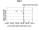
- the resistance valueAs illustrated in FIG. 7 , there is a threshold value of the resistance value as understood from a relationship between a resistance value of the Z electrode obtained from the circuit for use and the obtained signal.
- the horizontal axisrepresents a sheet resistance ( ⁇ / ⁇ ) of the Z electrode, and the vertical axis represents the signal component (relative value). It is preferable that the density of the conductive fine particles in the Z electrode be adjusted so that the plotted points exist in the right side region (high resistance) of FIG. 7 before the touch operation, and that the plotted points move to the left side region (low resistance) of FIG. 7 beyond the threshold value by the pressure of the touch.
- the nonconductive input meanscontacts the touch panel
- the Z electrode over the X electrode and the Y electrodeis compressed so that a resistance value thereof is changed.
- a capacity changemay be generated so that the input coordinates may be detected as an electrostatic capacity type.
Landscapes
- Engineering & Computer Science (AREA)
- General Engineering & Computer Science (AREA)
- Theoretical Computer Science (AREA)
- Human Computer Interaction (AREA)
- Physics & Mathematics (AREA)
- General Physics & Mathematics (AREA)
- Position Input By Displaying (AREA)
Abstract
Description
- The present application claims priority from Japanese application JP 2009-102777 filed on Apr. 21, 2009, the content of which is hereby incorporated by reference into this application.
- 1. Field of the Invention
- The present invention relates to an input device for inputting coordinates on a screen and a display device including the same. In particular, the present invention relates to an input device of an electrostatic capacity type that supports input using such an insulator as a plastic pen, and to a display device including the same.
- 2. Description of the Related Art
- A display device including an input device (hereinafter, also referred to as “touch sensor” or “touch panel”) having an on-screen input function of inputting information to a display screen by a touch operation (contact and press operation, hereinafter, simply referred to as “touch”) with a user's finger or the like is used for mobile electronic devices such as a PDA and a mobile terminal, various home electric appliances, a stationary customer guiding terminal such as an automatic reception machine, and the like. As a method for achieving the input device using the touch, there are known a resistance film method of detecting a change in resistance value of a touched portion, an electrostatic capacity method of detecting a change in capacity thereof, an optical sensor method of detecting a change in quantity of light at the portion shielded by the touch, and the like.
- The electrostatic capacity method has the following advantages when compared with the resistance film method or the optical sensor method. For example, a transmittance of the resistance film method or the optical sensor method is as low as 80%. On the other hand, a transmittance of the electrostatic capacity method is as high as about 90%, thereby preventing a reduction in displayed image quality. In the resistance film method, a touch position is detected by mechanical contact to the resistance film, thereby leading to possible deterioration or breakage (crack) of the resistance film. On the other hand, in the electrostatic capacity method, there is no mechanical contact such as contact of a detection electrode with another electrode. Thus, the electrostatic capacity method is advantageous in durability.
- An exemplary electrostatic capacity method is disclosed in JP 2003-511799 A (hereinafter, referred to as Patent Document 1). In the method disclosed therein, a vertical detection electrode (x electrode) and a horizontal detection electrode (Y electrode) are arranged in vertical and horizontal two-dimensional matrix, and a capacity of each electrode is detected by an input processing unit. When a conductor such as a finger touches a surface of the touch panel, the capacity of each electrode increases. Thus, the input processing unit detects the touch to calculate input coordinates based on a signal of a capacity change detected by each electrode. Even when the detection electrode is deteriorated to change its resistance value as physical characteristics, such an influence on capacity detection is limited. Thus, there is only a little influence on input position detection accuracy of the touch panel. As a result, high input position detection accuracy may be realized.
- In addition, JP 2004-5672 A describes a method of forming a high polymer layer containing conductive fine particles on a surface of a transparent electrode of a touch panel, thereby obtaining a superior antireflection effect and improving transparency.
- However, in the touch panel using the electrostatic capacity method, as described in
Patent Document 1, input coordinates are detected based on the capacity change of each detection electrode. Hence, input means needs to be a conductive substance. Here, a conductive substance is typified by a human finger, and the touch panel using the electrostatic capacity method is recognized as a touch panel for finger input. Thus, there is a problem in that, when a resin-made stylus as a nonconductive insulator used by the resistance film method is brought into contact with the touch panel using the electrostatic capacity method, almost no capacity change occurs in the electrode, which disables detection of the input coordinates. - On the other hand, in case that an input operation is performed on the touch panel using the electrostatic capacity method with the use of a stylus made of a conductive material such as a metal, the number of electrodes need to increase. For example, it is assumed that an electrostatic, capacity type touch panel having a diagonal size of 4 inches and a vertical and horizontal size ratio of 3:4 is realized in an electrode shape based on a diamond shape as described in
Patent Document 1. In the case of finger input, if a minimum contact surface has a diameter of 6 mm, and detection electrodes are prepared by using this size as an electrode interval, the total number of electrodes is 22. If a contact surface of the stylus has a diameter of 1 mm, and detection electrodes are prepared by using this size as an electrode interval, on the other hand, the total number of electrodes is 139, which indicates an increase of about six times. The increased number of electrodes causes an increase in frame area necessary for laying wiring lines connected to the input processing unit, and an increase in number of signal connections with a control circuit, consequently lowering reliability against shock and the like. Further, a circuit area increases due to an increase in number of terminals of the input processing unit, thereby leading to a fear of a cost increase. On the other hand, if a stylus with a tip made of conductive rubber is used, assuming the same total number of electrodes, a shape having a diameter of approximately 6 mm is necessary as a contact surface, with the result that input of characters may be accompanied with discomfort. - In view of the above, the electrostatic capacity type touch panel disclosed in
Patent Document 1 has a challenge to support an input with an insulating substance (support a stylus). - In order to meet the above-mentioned challenge, the present invention employs an electrostatic capacity type touch panel including: a plurality of X electrodes; a plurality of Y electrodes; and a Z electrode as a transparent elastic conductive resin layer. In the electrostatic capacity type touch panel, each of the plurality of X electrodes and each of the plurality of Y electrodes crosses each other via a first insulating layer, and are formed so as to alternately array pad portions and thin line portions in extending directions of the each of the plurality of X electrodes and the each of the plurality of Y electrodes. The pad portion of the each of the plurality of X electrodes and the pad portion of the each of the plurality of Y electrodes are disposed so as not to overlap each other in plan view. The Z electrode is a transparent electrically elastic conductive resin layer in which conductive fine particles are dispersed. Therefore, density of conductive fine particles that are dispersed thereinside is increased as the conductive fine particles clump by the pressure of touch, with the result that a resistance value of the Z electrode is decreased. Thus, even if nonconductive input means is used, a capacity change between the Z electrode (the part having the resistance value decreased by the pressure) and the X electrode as well as the Y electrode may be detected so that coordinates of the touched position may be determined.
- The electrostatic capacity type touch panel of the present invention may support an input by not only a finger but also an insulator such as a resin pen.
- In the accompanying drawings:
FIG. 1 is a system block diagram of an input device according to an embodiment of the present invention and a display device including the input device;FIG. 2 is a cross section illustrating an electrode structure of a touch panel according to the embodiment of the present invention;FIG. 3 is a cross section illustrating the electrode structure of the touch panel according to the embodiment of the present invention;FIGS. 4A and 4B are schematic diagrams illustrating a capacity change in an input operation by a finger in the touch panel according to the embodiment of the present invention;FIGS. 5A and 5B are schematic diagrams illustrating a capacity change in an input operation by a resin pen in the touch panel according to the embodiment of the present invention;FIG. 6 is a layout diagram of capacity detection electrodes in a touch panel; andFIG. 7 is a graph illustrating a resistance value of a Z electrode and signal intensity in the embodiment of the present invention.- Referring to the drawings, an embodiment of the present invention is described below in detail.
FIG. 1 illustrates configurations of an input device (hereinafter, referred to as touch panel) and a display device including the input device.- In
FIG. 1 , a touch panel according to a first embodiment of the present invention is represented by101. Thetouch panel 101 includes X and Y electrodes XP and YP for capacity detection. Four (XP1 to XP4) X electrodes and four (YP1 to YP4) Y electrodes, for example, are illustrated in this case. However, the numbers of electrodes are not limited thereto. Thetouch panel 101 is installed on a front side of adisplay portion 106 of a display device. Thus, when a user views an image displayed on thedisplay portion 106 of the display device, a transmittance of the touch panel is desirably high because the displayed image needs to pass through the touch panel. The X and Y electrodes of thetouch panel 101 are connected to acapacity detection unit 102 via detection wiring lines. Thecapacity detection unit 102 is controlled based on a detection control signal output from acontrol calculation unit 103 to detect a capacity of each electrode (each of X and Y electrodes) included in the touch panel, and to output a capacity detection signal changed depending on a capacity value of each electrode to thecontrol calculation unit 103. Thecontrol calculation unit 103 calculates a signal component of each electrode from the capacity detection signal of each electrode, and calculates input coordinates from the signal component of each electrode. Asystem 104 generates, when receiving the input coordinates transferred from thetouch panel 101 by a touch operation, a displayed image according to the touch operation, and transfers the displayed image as a display control signal to adisplay control circuit 105. Thedisplay control circuit 105 generates a display signal according to the displayed image transferred as the display control signal, and displays an image on thedisplay portion 106 of the display device. FIG. 2 illustrates a structure of the touch panel of this embodiment, illustrating a cross sectional shape of thetouch panel 101 from the point A to the point B ofFIG. 3 . This cross sectional view illustrates only layers that are necessary for description of an operation of the touch panel. InFIG. 2 , thetouch panel 101 includestransparent substrates layers 2 and3, a transparent elastic conductive resin layer4, and the detection electrodes XP, YP, and ZP.- The touch panel of this embodiment is a touch panel including the first
transparent substrate 1, on which the transparent conductive film XP, the first transparent insulatingfilm 2, the transparent conductive film YP, the second transparent insulating film3, and a transparent elastic conductive resin layer ZP4 in which conductive fine particles are dispersed are laminated in this order, and the secondtransparent substrate 5 is further formed thereon. - Next, the capacity detection electrodes that are provided to the
touch panel 101 according to the first embodiment of the present invention are described with reference toFIGS. 3 ,4A,4B,5A, and5B. FIG. 3 is a diagram illustrating an electrode pattern of the X electrodes XP and the Y electrodes YP for capacity detection in thetouch panel 101. The X electrodes XP and the Y electrodes YP are connected to thecapacity detection unit 102 via the detection wiring lines. The Y electrodes extend in the horizontal direction in thetouch panel 101, and a plurality of the Y electrodes are arranged in the vertical direction. At intersections of the Y electrodes and the X electrodes, electrode widths of the Y electrode and the X electrode are made thin in order to reduce cross capacity of each electrode. This portion is referred to as a thin line portion, temporarily. Therefore, the Y electrode has thin line portions and other electrode portions (hereinafter, referred to as pad portions) arranged alternately in the extending direction. Between neighboring Y electrodes, the X electrodes are arranged. The X electrodes extend in the vertical direction in thetouch panel 101, and a plurality of the X electrodes are arranged in the horizontal direction. Similarly to the Y electrodes, the X electrode also has thin line portions and the pad portions arranged alternately in the extending direction.- Next, a shape of the pad portion of the X electrode is described, assuming that a wiring position for connecting the X electrode to the detection wiring line (or the thin line portion of the X electrode) is the center of the X electrode in the horizontal direction. The pad portion of the X electrode has an electrode shape such that the area thereof becomes smaller as being closer to the center of the neighboring X electrode, while becoming larger as being closer to the center of the X electrode concerned. Therefore, considering an area of the X electrode between two neighboring X electrodes, e.g., an area between XP1 and XP2, the electrode area of the pad portion of the X electrode XP1 becomes maximum while the electrode area of the pad portion of the X electrode XP2 becomes minimum at the middle portion of the X electrode XP1. In contrast, at the middle portion of the X electrode XP2, the electrode area of the pad portion of the X electrode XP1 becomes minimum while the electrode area of the pad portion of the X electrode XP2 becomes maximum.
- Next, the layer structure of the
touch panel 101 is described in order of from the nearest layer to the farthest layer with respect to the firsttransparent substrate 1. The material, the thickness, and the like of the firsttransparent substrate 1 are not particularly limited and, depending on the application and use thereof, the firsttransparent substrate 1 is preferably selected from materials including inorganic glass such as barium borosilicate glass and soda glass, chemically strengthened glass, and resin films such as polyether sulfone (PES), polysulfone (PSF), polycarbonate (PC), polyarylate (PAR), and polyethylene terephthalate (PET). Further, the electrodes to be used for XP and YP are a transparent conductive film, which is not particularly limited as long as the electrode is a conductive thin film. Conventional examples which may be used include indium tin oxide (ITO), antimony tin oxide (ATO), and indium zinc oxide (IZO). The transparent conductive film (having a thickness of 50 to 200 Å) is formed, so as to make the surface resistance 500 to 2,000Ω, using a sputtering method, and patterning is conducted using an exposure and developing process after application of the resist material. Here, the resist material may be any one of a positive and a negative type, and may be easily formed with an alkali development type. After that, ITO is patterned to be formed by etching. Here, the etchant to be used is preferably selected from an aqueous hydrobromic acid solution or the like. - The X electrode XP is formed at a portion close to the first
transparent substrate 1, and then the first insulatingfilm 2 is formed for insulating the X electrode and the Y electrode from each other. Next, the Y electrode YP is formed. Here, the order of the X electrode XP and the Y electrode YP may be exchanged. After the Y electrode YP, the second insulating film3 is disposed so as to secure insulation between the Y electrodes YP and the Z electrode ZP to be disposed next. Film thicknesses of the first insulatingfilm 2 and the second insulating film3 are selected appropriately considering a dielectric constant of the insulating film material. It is easy to set the specific dielectric constant to a value from 2 to 4, and the film thickness may be set to a value from 1 to 20 μm. Used as a material of the insulating film layer is an ultraviolet (UV) curing resin material, a negative or positive insulating film material that may be developed with alkaline, or a thermosetting resin material that is cured by heat. The alkali development type may be formed easily. - The transparent elastic conductive resin layer4 is a resin layer in which conductive fine particles are dispersed. The dispersed individual fine particles are overlapped in the direction of the surface of the first transparent substrate and in the direction perpendicular to the surface, and the resin is disposed between the fine particles. The conductive fine particles are mixed in order that a resistance of the Z electrode ZP be lowered by the pressure applied by the pen so that a closed circuit is formed between XP1 and XP2 and the capacity change is transmitted. In addition, in order to obtain uniform pressure responsiveness in the entire surface of the
touch panel 101, it is preferable that the grain diameter be uniform, and fine particles having a spherical shape, a needle shape, a plate shape, or the like may be selected appropriately. In addition, the grain diameter of the conductive fine particle is selected from a range of 0.01 to 5 μm. As the conductive fine particles, it is sufficient that the conductive fine particles have at least a conductive layer on the surface. For example, metal fine particles made of nickel, gold, silver, copper, or the like, insulating inorganic fine particles, or resin fine particles coated with metal may be used. Further, fine particles made of at least one kind of metal oxide or metal fluoride selected from the group consisting of Al2O3, Bi2O3, CeO2, In2O3, (In2O3.SnO2), HfO2, La2O3, MgF2, Sb2O5, (Sb2O5.SnO2), SiO2, SnO2, TiO2, Y2O3, ZnO, and ZrO2may be used. In addition, fine particles of polyaniline, polyacetylene, polyethylene dioxythiophene, polypyrrole, polyisothianaphthene, polyisonaphthothiophene, and the like may also be used. As the fine particles, materials having low optical absorption and scattering as a result of optical refractive index and optical reflection are preferably appropriately selected. - A resin to be used in the resin layer with the dispersed conductive fine particles is particularly preferably a material having transparency and elasticity. However, the resin is not limited thereto and a material having a refractive index close to a transparent electrode is preferable in order to improve the transmittance. Examples of the material include butyl rubber, fluorocarbon rubber, ethylene-propylene-diene monomer rubber (EPDM), acrylonitrile-butadiene rubber (NBR), chloroprene rubber (CR), natural rubber (NR), isoprene rubber (IR), styrene-butadiene rubber (SBR), butadiene rubber, ethylene-propylene rubber, silicone rubber, polyurethane rubber, polynorbornene rubber, styrene-butadiene-styrene rubber, epichlorohydrin rubber, hydrogenated NBR, polysulfide rubber, and urethane rubber. Those rubbers may be used alone, or two or more kinds of them may be used in combination. Further examples of the material include polymer resins such as polyvinyl alcohol, an acrylic resin, and a urethane resin. The refractive index of those rubbers and resins is preferably in the range of 1.4 to 1.8, and the film thickness is preferably in the range of 0.5 to 200 μm.
- The material of the second
transparent substrate 1 is not limited to a particular material. But, because it is necessary to transmit the compression force of the pressing to the transparent elastic conductive resin layer4, it is not preferable to use inorganic glass such as barium borosilicate glass or soda glass, or chemically strengthened glass. It is preferable to select the material of the secondtransparent substrate 1 from resins having elasticity such as polyether sulf one (PBS), polysulfone (PSF), polycarbonate (PC), polyarylate (PAR), and polyethylene terephthalate (PET), and a material consisting of the resin and additional elastomer component for improving the elasticity. Using those materials, the stiffness becomes higher than that of the transparent elastic conductive resin layer4. Therefore, the pressure may be transmitted to the resin layer4 more easily. In addition, in order to satisfy the above-mentioned elasticity, it is preferable that the thickness of the secondtransparent substrate 5 be 800 μm or smaller. Further, if a film is used as the secondtransparent substrate 5, a deformation of the transparent elastic conductive resin layer4 becomes so large when a large load is imposed that the interface between the secondtransparent substrate 5 and the transparent elastic conductive resin layer4 is apt to be peeled. Therefore, it is preferable that the thickness of the secondtransparent substrate 5 be 100 μm or larger. - Next, the capacity change in the touch operation of the
touch panel 101 according to the first embodiment of the present invention is described with reference toFIGS. 4A ,4B,5A, and5B. FIGS. 4A and 4B are schematic diagrams illustrating the capacity change in the case where the input means of the touch operation is a conductor such as a finger. Here, it is assumed that the pressure of the touch operation is so small that the thickness of the transparent elastic conductive resin layer4 does not change. This assumption may be considered to be reasonable because a finger is soft and the contact surface is large. In addition, the electrode capacity of each electrode is a combined capacity of a fringe capacity with neighboring electrodes, a cross capacity, and other parasitic capacity, but here, only a parallel flat plate capacity with the Z electrode is noted while other electrode capacity is supposed to be unchanged between the touch operation and anon-touch operation.- When the electrode capacity of the X electrode XP1 is detected by the
capacity detection unit 102, the Y electrode YP2 becomes the GND potential in a reset state. Therefore, the combined capacity regarding the X electrode XP1 corresponds to a capacity Cf between the X electrode XP1 and the Y electrode YP2 via the finger as a conductor because the Z electrode ZPA has a high resistance. This case is similar to the capacity detection in the normal electrostatic capacity type touch panel. FIGS. 5A and 5B are schematic diagrams illustrating a capacity change in the case where the input means of the touch operation is nonconductive, and the thickness of the transparent elastic conductive resin layer4 changes by the pressure of the touch operation. Here, it is assumed that the pressure of the touch operation is so large that the thickness of the transparent elastic conductive resin layer4 changes at the touched portion. This assumption may be considered to be reasonable because the pen is hard and has a small contact surface. The capacity without the touch operation corresponds to a very small capacity between neighboring electrodes via the insulatingfilm 2 between the X electrode XP1 and the Y electrode YP2. When being touched with the pen, the transparent elastic conductive resin layer4 at the touched portion is compressed in the direction perpendicular to the surface of thetransparent substrate 1, with the result that a distance between the conductive fine particles dispersed inside the transparent elastic conductive resin layer4 is decreased in the vertical direction, resulting in increase of the density. As a result, the resistance value of the transparent elastic conductive resin layer4 at the touched portion is decreased. In the case where the resistance value of the Z electrode ZPA is decreased by the pressure in the touch operation, the capacity between the Z electrode ZPA and the X electrode XP1 is represented by Cxza, and the capacity between the Z electrode ZPA and the Y electrode YP2 is represented by Cyza. When thecapacity detection unit 102 detects the electrode capacity of the X electrode XP1, the Y electrode YP2 becomes the GND potential in the reset state. Therefore, the combined capacity regarding the X electrode XP1 is a capacity of Cxza and Cyza connected in series, because the Z electrode ZPA is in the floating state. The combined capacity Cxpa of the X electrode is expressed by the expression below.
Cxpa=Cxza·Cyza/(Cxza+Cyza) Expression (1)- The
control calculation unit 103 calculates an XP1 electrode capacity Cxpa in the touch operation as a signal component of the X electrode XP1. Electrode capacity values in the presence and the absence of the touch operation may be detected by thecapacity detection unit 102. Therefore, thecontrol calculation unit 103 may calculate the signal component of the X electrode XP1. - As described above, by using the Z electrode ZP as the transparent elastic conductive resin layer4, even if the nonconductive input means is used, the thickness of the transparent elastic conductive resin layer4 changes by the pressure so that the capacity changes. Thus, the input coordinates may be detected from the capacity change.
- In order to show the capacity detection effect due to the electrode shapes of the X electrode, the Y electrode, and the Z electrode in the above-mentioned first embodiment of the present invention, signal intensity values are measured by using the touch panel having a diagonal size of 4 inches (the aspect ratio is supposed to be 3:4) as illustrated in
FIG. 6 . InFIG. 6 , shapes of the X electrodes and the Y electrodes are simplified, but actually, the X electrodes and the Y electrodes having the shapes illustrated inFIG. 3 are arranged at electrode intervals illustrated inFIG. 6 . - The density of the conductive fine particles dispersed in the transparent elastic conductive resin layer4 may be adjusted based on a film thickness of the second insulating layer3, a dielectric constant thereof, a film thickness of the transparent elastic conductive resin layer4, and a detection circuit as appropriate. It is preferable to set to a low density in order to avoid light scattering and a decrease in transmittance due to concentration of the conductive fine particles.
- As illustrated in
FIG. 7 , there is a threshold value of the resistance value as understood from a relationship between a resistance value of the Z electrode obtained from the circuit for use and the obtained signal. The horizontal axis represents a sheet resistance (Ω/□) of the Z electrode, and the vertical axis represents the signal component (relative value). It is preferable that the density of the conductive fine particles in the Z electrode be adjusted so that the plotted points exist in the right side region (high resistance) ofFIG. 7 before the touch operation, and that the plotted points move to the left side region (low resistance) ofFIG. 7 beyond the threshold value by the pressure of the touch. - As described above, according to the embodiment of the present invention, even in the case where the nonconductive input means contacts the touch panel, in addition to the X electrode and the Y electrode for capacity detection, and the Z electrode over the X electrode and the Y electrode is compressed so that a resistance value thereof is changed. Thus, a capacity change may be generated so that the input coordinates may be detected as an electrostatic capacity type.
- While there have been described what are at present considered to be certain embodiments of the invention, it will be understood that various modifications may be made thereto, and it is intended that the appended claims cover all such modifications as fall within the true spirit and scope of the invention.
Claims (10)
Applications Claiming Priority (2)
| Application Number | Priority Date | Filing Date | Title |
|---|---|---|---|
| JP2009102777AJP5039747B2 (en) | 2009-04-21 | 2009-04-21 | Input device and display device including the same |
| JP2009-102777 | 2009-04-21 |
Publications (2)
| Publication Number | Publication Date |
|---|---|
| US20100265212A1true US20100265212A1 (en) | 2010-10-21 |
| US8537136B2 US8537136B2 (en) | 2013-09-17 |
Family
ID=42980651
Family Applications (1)
| Application Number | Title | Priority Date | Filing Date |
|---|---|---|---|
| US12/761,425Active2031-02-19US8537136B2 (en) | 2009-04-21 | 2010-04-16 | Input device and display device including the same |
Country Status (2)
| Country | Link |
|---|---|
| US (1) | US8537136B2 (en) |
| JP (1) | JP5039747B2 (en) |
Cited By (29)
| Publication number | Priority date | Publication date | Assignee | Title |
|---|---|---|---|---|
| US20100253651A1 (en)* | 2009-04-06 | 2010-10-07 | Synaptics Incorporated | Input device with deflectable electrode |
| US20100308844A1 (en)* | 2009-06-03 | 2010-12-09 | Synaptics Incorporated | Input device and method with pressure-sensitive layer |
| US20110175671A1 (en)* | 2010-01-15 | 2011-07-21 | Synaptics Incorporated | Input device with floating electrodes having at least one aperture |
| US20110273394A1 (en)* | 2010-05-10 | 2011-11-10 | Symbol Technologies, Inc. | Methods and apparatus for a transparent and flexible force-sensitive touch panel |
| US20110298725A1 (en)* | 2010-06-03 | 2011-12-08 | J Touch Corporation | Touch panel manufacturing method and structure thereof |
| EP2515218A1 (en)* | 2011-04-21 | 2012-10-24 | Innovation & Infinity Global Corp. | Transparent conductive structure applied to a touch panel and method of making the same |
| EP2515217A1 (en)* | 2011-04-21 | 2012-10-24 | Innovation & Infinity Global Corp. | Transparent conductive structure applied to a touch panel and method of making the same |
| US20130215035A1 (en)* | 2012-02-21 | 2013-08-22 | David Brent GUARD | Flexible Touch Sensor Input Device |
| US20140028569A1 (en)* | 2012-07-24 | 2014-01-30 | David Brent GUARD | Dielectric Layer for Touch Sensor Stack |
| US20140028570A1 (en)* | 2012-07-24 | 2014-01-30 | David Brent GUARD | Dielectric Layer for Touch Sensor Stack |
| US20140043289A1 (en)* | 2012-08-07 | 2014-02-13 | N-Trig Ltd. | Capacitive sensor for a digitizer system |
| US20140092324A1 (en)* | 2012-09-28 | 2014-04-03 | Samsung Corning Precision Materials Co., Ltd. | Transparent conductive substrate and touch panel having the same |
| US20140132553A1 (en)* | 2012-11-14 | 2014-05-15 | Samsung Display Co., Ltd. | Flexible touch screen panel and flexible display device with the same |
| US20140168146A1 (en)* | 2012-12-14 | 2014-06-19 | Panasonic Corporation | Touch panel |
| US8866779B2 (en) | 2012-04-18 | 2014-10-21 | Japan Display Inc. | Display device |
| US8878768B2 (en) | 2012-04-19 | 2014-11-04 | Japan Display Inc. | Display device |
| US20140375604A1 (en)* | 2013-06-25 | 2014-12-25 | Japan Display Inc. | Liquid crystal display device with touch panel |
| US20150212603A1 (en)* | 2014-01-29 | 2015-07-30 | Netanel Raisch | Methods and devices for transferring a tactile signal through a solid element |
| US20150253900A1 (en)* | 2014-03-07 | 2015-09-10 | Alps Electric Co., Ltd. | Electrostatic capacitance-type input device |
| US9471188B2 (en) | 2013-10-02 | 2016-10-18 | Japan Display Inc. | Liquid crystal display device with touch panel |
| US9798429B2 (en) | 2014-02-28 | 2017-10-24 | Synaptics Incorporated | Guard electrodes in a sensing stack |
| US10133421B2 (en) | 2014-04-02 | 2018-11-20 | Synaptics Incorporated | Display stackups for matrix sensor |
| US10234996B2 (en) | 2014-06-23 | 2019-03-19 | Microsoft Technology Licensing, Llc | Capacitive based digitizer sensor |
| US10254894B2 (en) | 2015-12-23 | 2019-04-09 | Cambridge Touch Technologies Ltd. | Pressure-sensitive touch panel |
| US10282046B2 (en) | 2015-12-23 | 2019-05-07 | Cambridge Touch Technologies Ltd. | Pressure-sensitive touch panel |
| US10310659B2 (en) | 2014-12-23 | 2019-06-04 | Cambridge Touch Technologies Ltd. | Pressure-sensitive touch panel |
| US10318038B2 (en) | 2014-12-23 | 2019-06-11 | Cambridge Touch Technologies Ltd. | Pressure-sensitive touch panel |
| US10817116B2 (en) | 2017-08-08 | 2020-10-27 | Cambridge Touch Technologies Ltd. | Device for processing signals from a pressure-sensing touch panel |
| US11093088B2 (en) | 2017-08-08 | 2021-08-17 | Cambridge Touch Technologies Ltd. | Device for processing signals from a pressure-sensing touch panel |
Families Citing this family (6)
| Publication number | Priority date | Publication date | Assignee | Title |
|---|---|---|---|---|
| JP5349176B2 (en)* | 2009-07-09 | 2013-11-20 | 三菱自動車工業株式会社 | Touch switch device |
| JP5295914B2 (en)* | 2009-09-18 | 2013-09-18 | 株式会社ジャパンディスプレイ | Display device |
| JP5439114B2 (en) | 2009-10-21 | 2014-03-12 | 株式会社ジャパンディスプレイ | Capacitance type input device and electro-optical device with input device |
| JP5445438B2 (en)* | 2010-12-15 | 2014-03-19 | Smk株式会社 | Capacitive touch panel |
| JP5837832B2 (en)* | 2012-01-20 | 2015-12-24 | 富士フイルム株式会社 | Substrate on which a photocurable resin layer is formed, method for forming the same, capacitance-type input device, and image display device |
| CN107407997A (en)* | 2015-02-27 | 2017-11-28 | 株式会社藤仓 | Touch sensor, which is used, matches somebody with somebody wire body, touch sensor wiring substrate and touch sensor |
Citations (4)
| Publication number | Priority date | Publication date | Assignee | Title |
|---|---|---|---|---|
| US6297811B1 (en)* | 1999-06-02 | 2001-10-02 | Elo Touchsystems, Inc. | Projective capacitive touchscreen |
| US20080122802A1 (en)* | 2006-11-29 | 2008-05-29 | Tsutomu Furuhashi | Liquid crystal dispaly device with touch screen |
| US20090256821A1 (en)* | 2008-04-15 | 2009-10-15 | Norio Mamba | Display device |
| US20120044187A1 (en)* | 2009-03-29 | 2012-02-23 | Cypress Semiconductor Corporation | Capacitive Touch Screen |
Family Cites Families (5)
| Publication number | Priority date | Publication date | Assignee | Title |
|---|---|---|---|---|
| JPS58211241A (en)* | 1982-05-31 | 1983-12-08 | Fujitsu Ltd | Touch type coordinate detection panel |
| JPH1063402A (en)* | 1996-08-26 | 1998-03-06 | Matsushita Electric Ind Co Ltd | Coordinate position input device |
| US7030860B1 (en) | 1999-10-08 | 2006-04-18 | Synaptics Incorporated | Flexible transparent touch sensing system for electronic devices |
| JP4626897B2 (en)* | 2000-01-27 | 2011-02-09 | シャープ株式会社 | Input device |
| JP2004005672A (en) | 2003-05-19 | 2004-01-08 | Seiko Epson Corp | Touch panel and display device with touch panel |
- 2009
- 2009-04-21JPJP2009102777Apatent/JP5039747B2/enactiveActive
- 2010
- 2010-04-16USUS12/761,425patent/US8537136B2/enactiveActive
Patent Citations (4)
| Publication number | Priority date | Publication date | Assignee | Title |
|---|---|---|---|---|
| US6297811B1 (en)* | 1999-06-02 | 2001-10-02 | Elo Touchsystems, Inc. | Projective capacitive touchscreen |
| US20080122802A1 (en)* | 2006-11-29 | 2008-05-29 | Tsutomu Furuhashi | Liquid crystal dispaly device with touch screen |
| US20090256821A1 (en)* | 2008-04-15 | 2009-10-15 | Norio Mamba | Display device |
| US20120044187A1 (en)* | 2009-03-29 | 2012-02-23 | Cypress Semiconductor Corporation | Capacitive Touch Screen |
Cited By (46)
| Publication number | Priority date | Publication date | Assignee | Title |
|---|---|---|---|---|
| US20100253651A1 (en)* | 2009-04-06 | 2010-10-07 | Synaptics Incorporated | Input device with deflectable electrode |
| US9459734B2 (en) | 2009-04-06 | 2016-10-04 | Synaptics Incorporated | Input device with deflectable electrode |
| US20100308844A1 (en)* | 2009-06-03 | 2010-12-09 | Synaptics Incorporated | Input device and method with pressure-sensitive layer |
| US9383881B2 (en) | 2009-06-03 | 2016-07-05 | Synaptics Incorporated | Input device and method with pressure-sensitive layer |
| US20110175671A1 (en)* | 2010-01-15 | 2011-07-21 | Synaptics Incorporated | Input device with floating electrodes having at least one aperture |
| US8653834B2 (en) | 2010-01-15 | 2014-02-18 | Synaptics Incorporated | Input device with floating electrodes having at least one aperture |
| US20110273394A1 (en)* | 2010-05-10 | 2011-11-10 | Symbol Technologies, Inc. | Methods and apparatus for a transparent and flexible force-sensitive touch panel |
| US20110298725A1 (en)* | 2010-06-03 | 2011-12-08 | J Touch Corporation | Touch panel manufacturing method and structure thereof |
| EP2515217A1 (en)* | 2011-04-21 | 2012-10-24 | Innovation & Infinity Global Corp. | Transparent conductive structure applied to a touch panel and method of making the same |
| EP2515218A1 (en)* | 2011-04-21 | 2012-10-24 | Innovation & Infinity Global Corp. | Transparent conductive structure applied to a touch panel and method of making the same |
| US20130215035A1 (en)* | 2012-02-21 | 2013-08-22 | David Brent GUARD | Flexible Touch Sensor Input Device |
| US9471185B2 (en)* | 2012-02-21 | 2016-10-18 | Atmel Corporation | Flexible touch sensor input device |
| US8866779B2 (en) | 2012-04-18 | 2014-10-21 | Japan Display Inc. | Display device |
| US10303294B2 (en) | 2012-04-19 | 2019-05-28 | Japan Display Inc. | Display device |
| US9563307B2 (en) | 2012-04-19 | 2017-02-07 | Japan Display Inc. | Display device |
| US9766748B2 (en) | 2012-04-19 | 2017-09-19 | Japan Display Inc. | Display device |
| US10198117B2 (en) | 2012-04-19 | 2019-02-05 | Japan Display Inc. | Display device |
| US8878768B2 (en) | 2012-04-19 | 2014-11-04 | Japan Display Inc. | Display device |
| US9223434B2 (en) | 2012-04-19 | 2015-12-29 | Japan Display Inc. | Display device |
| US20140028570A1 (en)* | 2012-07-24 | 2014-01-30 | David Brent GUARD | Dielectric Layer for Touch Sensor Stack |
| US9116584B2 (en)* | 2012-07-24 | 2015-08-25 | Atmel Corporation | Dielectric layer for touch sensor stack |
| US20140028569A1 (en)* | 2012-07-24 | 2014-01-30 | David Brent GUARD | Dielectric Layer for Touch Sensor Stack |
| US9098152B2 (en)* | 2012-07-24 | 2015-08-04 | Atmel Corporation | Dielectric layer for touch sensor stack |
| US20140043289A1 (en)* | 2012-08-07 | 2014-02-13 | N-Trig Ltd. | Capacitive sensor for a digitizer system |
| US20140092324A1 (en)* | 2012-09-28 | 2014-04-03 | Samsung Corning Precision Materials Co., Ltd. | Transparent conductive substrate and touch panel having the same |
| CN103713765A (en)* | 2012-09-28 | 2014-04-09 | 三星康宁精密素材株式会社 | Transparent conductive substrate and touch panel having the same |
| US10067623B2 (en) | 2012-11-14 | 2018-09-04 | Samsung Display Co., Ltd. | Flexible touch screen panel and flexible display device with the same |
| US10768757B2 (en) | 2012-11-14 | 2020-09-08 | Samsung Display Co., Ltd. | Flexible touch screen panel and flexible display device with the same |
| US20140132553A1 (en)* | 2012-11-14 | 2014-05-15 | Samsung Display Co., Ltd. | Flexible touch screen panel and flexible display device with the same |
| US20140168146A1 (en)* | 2012-12-14 | 2014-06-19 | Panasonic Corporation | Touch panel |
| US9373295B2 (en)* | 2013-06-25 | 2016-06-21 | Japan Display Inc. | Liquid crystal display device with touch panel |
| US20140375604A1 (en)* | 2013-06-25 | 2014-12-25 | Japan Display Inc. | Liquid crystal display device with touch panel |
| US9471188B2 (en) | 2013-10-02 | 2016-10-18 | Japan Display Inc. | Liquid crystal display device with touch panel |
| US9389739B2 (en)* | 2014-01-29 | 2016-07-12 | Netanel Raisch | Methods and devices for transferring a tactile signal through a solid element |
| US20150212603A1 (en)* | 2014-01-29 | 2015-07-30 | Netanel Raisch | Methods and devices for transferring a tactile signal through a solid element |
| US9798429B2 (en) | 2014-02-28 | 2017-10-24 | Synaptics Incorporated | Guard electrodes in a sensing stack |
| US20150253900A1 (en)* | 2014-03-07 | 2015-09-10 | Alps Electric Co., Ltd. | Electrostatic capacitance-type input device |
| US9971460B2 (en)* | 2014-03-07 | 2018-05-15 | Alps Electric Co., Ltd. | Electrostatic capacitance-type input device |
| US10133421B2 (en) | 2014-04-02 | 2018-11-20 | Synaptics Incorporated | Display stackups for matrix sensor |
| US10234996B2 (en) | 2014-06-23 | 2019-03-19 | Microsoft Technology Licensing, Llc | Capacitive based digitizer sensor |
| US10310659B2 (en) | 2014-12-23 | 2019-06-04 | Cambridge Touch Technologies Ltd. | Pressure-sensitive touch panel |
| US10318038B2 (en) | 2014-12-23 | 2019-06-11 | Cambridge Touch Technologies Ltd. | Pressure-sensitive touch panel |
| US10254894B2 (en) | 2015-12-23 | 2019-04-09 | Cambridge Touch Technologies Ltd. | Pressure-sensitive touch panel |
| US10282046B2 (en) | 2015-12-23 | 2019-05-07 | Cambridge Touch Technologies Ltd. | Pressure-sensitive touch panel |
| US10817116B2 (en) | 2017-08-08 | 2020-10-27 | Cambridge Touch Technologies Ltd. | Device for processing signals from a pressure-sensing touch panel |
| US11093088B2 (en) | 2017-08-08 | 2021-08-17 | Cambridge Touch Technologies Ltd. | Device for processing signals from a pressure-sensing touch panel |
Also Published As
| Publication number | Publication date |
|---|---|
| US8537136B2 (en) | 2013-09-17 |
| JP5039747B2 (en) | 2012-10-03 |
| JP2010256956A (en) | 2010-11-11 |
Similar Documents
| Publication | Publication Date | Title |
|---|---|---|
| US8537136B2 (en) | Input device and display device including the same | |
| KR101138627B1 (en) | Input device and display device having the same | |
| US8605045B2 (en) | Touch panel and display device using the same | |
| JP5403815B2 (en) | Input device and display device including the same | |
| US20100271328A1 (en) | Input device and display device having the same | |
| JP5496851B2 (en) | Touch panel | |
| US8581123B2 (en) | Touch panel | |
| US8704796B2 (en) | Touch panel and display device | |
| US9354752B2 (en) | Sensor apparatus and information processing apparatus | |
| US20090278815A1 (en) | Touch panel | |
| JP2015079526A (en) | Capacitive touch panel, and reduction method of visibility of metal jumper on capacitive touch panel | |
| JP5520633B2 (en) | Display device with touch panel | |
| JP2012084025A (en) | Display device with touch panel | |
| KR20150095394A (en) | Touch window | |
| KR20150072838A (en) | Touch panel | |
| EP2713249B1 (en) | Touch display module and handheld electronic apparatus | |
| KR20100019810A (en) | Touch screen system | |
| US20110080368A1 (en) | Input device of touch screen and method of manufacturing the same | |
| US11507241B2 (en) | Touch panel, display device, and input device having shielding for touch sensing electrodes and/or pressure sensing electrodes | |
| KR102008736B1 (en) | Touch panel and method for driving the same | |
| KR101494259B1 (en) | Composite touch pannel with appendix and method for detecting touch using therefor | |
| US11379075B1 (en) | Electronic device and touch detection method | |
| KR20140039795A (en) | Touch panel and manufacturing method for the same | |
| CN110580114A (en) | In-cell touch display panel | |
| CN110998495A (en) | Touch screen |
Legal Events
| Date | Code | Title | Description |
|---|---|---|---|
| AS | Assignment | Owner name:HITACHI DISPLAYS, LTD., JAPAN Free format text:ASSIGNMENT OF ASSIGNORS INTEREST;ASSIGNORS:SEKIGUCHI, SHINJI;NAGATA, KOJI;HAYAKAWA, KOUJI;SIGNING DATES FROM 20100422 TO 20100427;REEL/FRAME:024542/0685 | |
| AS | Assignment | Owner name:IPS ALPHA SUPPORT CO., LTD., JAPAN Free format text:COMPANY SPLIT PLAN TRANSFERRING FIFTY (50) PERCENT SHARE IN PATENT APPLICATIONS;ASSIGNOR:HITACHI DISPLAYS, LTD.;REEL/FRAME:027092/0684 Effective date:20100630 Owner name:PANASONIC LIQUID CRYSTAL DISPLAY CO., LTD., JAPAN Free format text:MERGER;ASSIGNOR:IPS ALPHA SUPPORT CO., LTD.;REEL/FRAME:027093/0937 Effective date:20101001 | |
| STCF | Information on status: patent grant | Free format text:PATENTED CASE | |
| FEPP | Fee payment procedure | Free format text:PAYOR NUMBER ASSIGNED (ORIGINAL EVENT CODE: ASPN); ENTITY STATUS OF PATENT OWNER: LARGE ENTITY | |
| FPAY | Fee payment | Year of fee payment:4 | |
| MAFP | Maintenance fee payment | Free format text:PAYMENT OF MAINTENANCE FEE, 8TH YEAR, LARGE ENTITY (ORIGINAL EVENT CODE: M1552); ENTITY STATUS OF PATENT OWNER: LARGE ENTITY Year of fee payment:8 | |
| AS | Assignment | Owner name:JAPAN DISPLAY EAST INC., JAPAN Free format text:CHANGE OF NAME;ASSIGNOR:HITACHI DISPLAYS, LTD.;REEL/FRAME:063297/0222 Effective date:20120401 | |
| AS | Assignment | Owner name:JAPAN DISPLAY INC., JAPAN Free format text:CHANGE OF NAME;ASSIGNOR:JAPAN DISPLAY EAST INC.;REEL/FRAME:063327/0210 Effective date:20130401 | |
| AS | Assignment | Owner name:PANASONIC INTELLECTUAL PROPERTY CORPORATION OF AMERICA, CALIFORNIA Free format text:NUNC PRO TUNC ASSIGNMENT;ASSIGNOR:PANASONIC LIQUID CRYSTAL DISPLAY CO., LTD.;REEL/FRAME:065615/0327 Effective date:20230828 | |
| AS | Assignment | Owner name:PANELTOUCH TECHNOLOGIES LLC, TEXAS Free format text:ASSIGNMENT OF ASSIGNORS INTEREST;ASSIGNORS:PANASONIC INTELLECTUAL PROPERTY CORPORATION OF AMERICA;JAPAN DISPLAY INC.;REEL/FRAME:067245/0560 Effective date:20240322 | |
| FEPP | Fee payment procedure | Free format text:MAINTENANCE FEE REMINDER MAILED (ORIGINAL EVENT CODE: REM.); ENTITY STATUS OF PATENT OWNER: LARGE ENTITY |