US20100264953A1 - Soft Error Hard Electronic Circuit and Layout - Google Patents
Soft Error Hard Electronic Circuit and LayoutDownload PDFInfo
- Publication number
- US20100264953A1 US20100264953A1US12/763,139US76313910AUS2010264953A1US 20100264953 A1US20100264953 A1US 20100264953A1US 76313910 AUS76313910 AUS 76313910AUS 2010264953 A1US2010264953 A1US 2010264953A1
- Authority
- US
- United States
- Prior art keywords
- type
- mosfet
- circuit
- mosfets
- nodes
- Prior art date
- Legal status (The legal status is an assumption and is not a legal conclusion. Google has not performed a legal analysis and makes no representation as to the accuracy of the status listed.)
- Granted
Links
Images


Classifications
- H—ELECTRICITY
- H03—ELECTRONIC CIRCUITRY
- H03K—PULSE TECHNIQUE
- H03K19/00—Logic circuits, i.e. having at least two inputs acting on one output; Inverting circuits
- H03K19/003—Modifications for increasing the reliability for protection
- H03K19/0033—Radiation hardening
- H03K19/00338—In field effect transistor circuits
- G—PHYSICS
- G06—COMPUTING OR CALCULATING; COUNTING
- G06F—ELECTRIC DIGITAL DATA PROCESSING
- G06F30/00—Computer-aided design [CAD]
- G06F30/30—Circuit design
- G06F30/39—Circuit design at the physical level
- H—ELECTRICITY
- H10—SEMICONDUCTOR DEVICES; ELECTRIC SOLID-STATE DEVICES NOT OTHERWISE PROVIDED FOR
- H10D—INORGANIC ELECTRIC SEMICONDUCTOR DEVICES
- H10D84/00—Integrated devices formed in or on semiconductor substrates that comprise only semiconducting layers, e.g. on Si wafers or on GaAs-on-Si wafers
- H10D84/90—Masterslice integrated circuits
- H10D84/903—Masterslice integrated circuits comprising field effect technology
- H10D84/907—CMOS gate arrays
- H—ELECTRICITY
- H10—SEMICONDUCTOR DEVICES; ELECTRIC SOLID-STATE DEVICES NOT OTHERWISE PROVIDED FOR
- H10D—INORGANIC ELECTRIC SEMICONDUCTOR DEVICES
- H10D89/00—Aspects of integrated devices not covered by groups H10D84/00 - H10D88/00
- H10D89/10—Integrated device layouts
- G—PHYSICS
- G06—COMPUTING OR CALCULATING; COUNTING
- G06F—ELECTRIC DIGITAL DATA PROCESSING
- G06F2119/00—Details relating to the type or aim of the analysis or the optimisation
- G06F2119/18—Manufacturability analysis or optimisation for manufacturability
- Y—GENERAL TAGGING OF NEW TECHNOLOGICAL DEVELOPMENTS; GENERAL TAGGING OF CROSS-SECTIONAL TECHNOLOGIES SPANNING OVER SEVERAL SECTIONS OF THE IPC; TECHNICAL SUBJECTS COVERED BY FORMER USPC CROSS-REFERENCE ART COLLECTIONS [XRACs] AND DIGESTS
- Y02—TECHNOLOGIES OR APPLICATIONS FOR MITIGATION OR ADAPTATION AGAINST CLIMATE CHANGE
- Y02P—CLIMATE CHANGE MITIGATION TECHNOLOGIES IN THE PRODUCTION OR PROCESSING OF GOODS
- Y02P90/00—Enabling technologies with a potential contribution to greenhouse gas [GHG] emissions mitigation
- Y02P90/02—Total factory control, e.g. smart factories, flexible manufacturing systems [FMS] or integrated manufacturing systems [IMS]
Definitions
- This inventioncomprises a layout method to effectively protect logic circuits against soft errors (non-destructive errors) and circuit cells, with layout, which are protected against soft errors.
- TMRtriple mode redundancy
- BiSERbuilt-in soft-error resilience
- Error correction codes, ECC, for memorywhich also (loosely) could be classified as RHBD, is more efficient than duplication/triplication and can, with additional overhead, handle multiple errors in memory circuitry.
- ECCError correction codes
- RHBDError correction codes
- the application of a corresponding error correction to logic circuitsis very limited and application specific (e.g., selective parity check or insertion of specialized checking circuit IP).
- This inventioncomprises a layout method to effectively protect electronic circuits against soft errors (non-destructive errors) and circuit cells, with layout, which are protected against soft errors. It is based on U.S. patent application Ser. No. 12/354,655.
- the inventionapplies the method of 12/354,655 to sequential and combinational logic to generate specific circuit cells with netlists and layouts which are hard against single event generated soft-errors. It also devices methods of how two or more such cells should be laid out and placed relative to each other, in order to have the best global soft-error protection.
- FIG. 1Primary opposing nodes in a latch cell.
- FIG. 2A principal arrangement of opposing node of a latch circuit.
- FIG. 3Basic netlist for the DICE latch cell (prior art [Nic05]) with nodes 1 - 4 .
- p 1 -p 4 and n 1 -n 4are the pMOSFET drains and the nMOSFET drains, respectively.
- FIG. 4A first preferred layout arrangement for the layout of the DICE latch cell.
- ns/psare the source contacts for the two mosfets who's drains are adjacent.
- p 1 -p 4 and n 1 -n 4are the pMOSFET drains and the nMOSFET drains of the 4 main storage nodes, respectively. Any cyclic simultaneous permutation of the n and p nodes will be equivalent (and part of the invention).
- the mosfetscan be placed in separate active areas, or the adjacent n and p nodes can be placed in the same active area.
- the MOSFET sourcescan be placed in the line of the drains or in the direction vertical to the line of the drain nodes.
- the well contactscan be placed on either side only, or also surround the adjacent node pairs.
- the nodescan also be arranged in a different order subject to the following rules: two adjacent n-drains, or two adjacent p-drains are always an odd/even pair (e.g., p 1 & p 2 , or n 2 and n 3 ), adjacent n-drain to p-drain are always an odd/odd or and even/even pair (e.g., n 2 & p 2 , or p 3 & n 1 ).
- FIG. 5Net-list corresponding to the second preferred arrangement.
- the yellow MOSFETmay or may not be included, as long as node 6 is connected to drain 6 a in FIG. 5 , and p 1 and 6 a are physically separate.
- FIG. 6A second preferred layout arrangement. ns/ps are the source contacts for the two mosfets whose drains are adjacent. Node 6 a and 6 b are connected. The yellow gate adjacent to node 6 a may or may not be included (both variants included in the claims), but p 1 and 6 a are physically separate.
- the layoutderives from the layout in FIG. 1 , and the same variants w.r.t. node permutations, active, source, and well contact arrangements apply.
- FIG. 7Net-list corresponding to the third preferred arrangement.
- the yellow MOSFETmay or may not be included, as long as node 6 is connected to drain 6 a in FIG. 4 , and p 1 and 6 a are physically separate, and node 7 is connected to drain 7 a in FIG. 4 , and n 1 and 7 a are physically separate.
- FIG. 8A third preferred layout arrangement. ns/ps are the source contacts for the two mosfets who's drains are adjacent. Node 6 a - 6 b are connected, as are node 7 a / 7 b .
- the yellow gate adjacent to node 6 a and 7 amay or may not be included (both variants included in the claims), but the adjacent drain areas are physically separate.
- the layoutderives from the layout in FIG. 1 , and the same variants w.r.t. node permutations, active, source, and well contact arrangements apply.
- FIG. 9Net-list corresponding to the fourth preferred arrangement.
- the yellow MOSFETmay or may not be included, as long as node 6 is connected to drain 6 a , 7 to 7 a , 8 to 8 a , and 9 to 9 a in FIGS. 8 , and 6 a , 7 a , 8 a , 9 a are physically separate from their adjacent main drain node.
- FIG. 10A fourth preferred layout arrangement.
- ns/psare the source contacts for the two mosfets whose drains are adjacent.
- Node 6 a / 6 b , 7 a / 7 b , 8 a / 8 b , and 9 a / 9 bare connected.
- the yellow gates adjacent to nodes 6 a , 7 a , 8 a , 9 amay or may not be included (both variants included in the claims), but nodes 6 a , 7 a , 8 a , 9 a are physically separate from their adjacent MOSFET drains.
- the layoutderives from the layout in FIG. 1 , and the same variants w.r.t.
- node permutations, active, source, and well contact arrangementsapply.
- the claimsalso cover the various additional variants where and combination of the extra nodes 6 a / 6 b , 7 a / 7 b , 8 a / 8 b , 9 a / 9 b have been included or omitted.
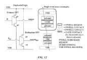
- FIG. 11Circuit schematic and layout for duplicated latch cells (e.g. for BISER) using placement and sizing to ensure complete hardness against single and multiple node single event effects.
- the primary latchcan only be upset when node 1 is HIGH
- the redundant latchcan only be upset when node 1 ( r ) is LOW.
- any single event that affects both latchescan only upset one of the two latches in the BISER configuration, and therefore, cannot generate an error.
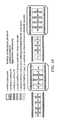
- FIG. 12Example of a duplicated circuit of claims 9 AND 10 .
- error signals on both primary and redundant nodescan be generated if both ndrain 0 and pdrain 1 are affected (if D is high) or if both ndrain 1 and pdrain 0 are affected (D low).
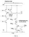
- FIG. 13Example of a adding protective MOSFET devices to a c-element filter circuit.
- the ndrain of the output of the c-elementi.e., a net which becomes floating if the two inputs have different voltage states
- the protection MOSFET n 1is connected, via the protection MOSFET n 1 , either to an n-type contact area close to the ndrain of the input net 2 , or via a second protective MOSFET, n 2 , to the ndrain of the input net 2 .
- FIG. 14Basic netlist for the DICE latch cell (prior art) with nodes 1 - 4 .
- p 1 -p 4 and n 1 -n 4are the pMOSFET drains and the nMOSFET drains, respectively.
- FIG. 15Arrangement 1 of the nodes in a layout for the DICE schematics in FIG. 14 .
- the nodes n 1 -n 4are the n-type MOSFET drains, and p 1 -p 4 the p-type MOSFET drains, that are connected to node 1 - 4 respectively.
- FIG. 16Arrangement 2 of the nodes in a layout for the DICE schematics in FIG. 14 .
- the nodes n 1 -n 4are the n-type MOSFET drains, and p 1 -p 4 the p-type MOSFET drains, that are connected to node 1 - 4 respectively.
- FIG. 17Arrangement 3 of the nodes in a layout for the DICE schematics in FIG. 14 .
- the nodes n 1 -n 4are the n-type MOSFET drains, and p 1 -p 4 the p-type MOSFET drains, that are connected to node 1 - 4 respectively.
- FIG. 18Arrangement 4 of the nodes in a layout for the DICE schematics in FIG. 14 .
- the nodes n 1 -n 4are the n-type MOSFET drains, and p 1 -p 4 the p-type MOSFET drains, that are connected to node 1 - 4 respectively.
- FIG. 19Arrangement 5 of the nodes in a layout for the DICE schematics in FIG. 14 .
- the nodes n 1 -n 4are the n-type MOSFET drains, and p 1 -p 4 the p-type MOSFET drains, that are connected to node 1 - 4 respectively.
- FIG. 20Dual interlocked cell (DICE) latch with symmetric clocking D, and Dinv, are the data input and inverse of data input, respectively, CLK is the clock, and CLKB 1 and CLKB 2 are the inverse of the CLK.
- the inverse of the CLKis here included as two separate signals CLKB 1 and CLKB 2 , the claims also cover the case where CLKB 1 and CLKB 2 are the same signal (e.g., if a CLKB is provided external to the cell).
- FIG. 21Layout arrangement of the contact drain areas of the first, second, and third additional MOSFET for one of the ordering configurations of the net 1 , 2 , 3 , and 4 , for the DICE schematics in FIG. 20 .
- the nodes n 1 -n 4are the n-type MOSFET drains, and p 1 -p 4 the p-type MOSFET drains, that are connected to node 1 - 4 respectively.
- the drain areas of the additional MOSFETsare either shared with, or placed adjacent to, the drain contact area of the MOSFET, or the same type, to which they are connected.
- the signals Dinv, CLKB 1 , CLKB 2(Dinv is the inverse of the data signal, CLKB 1 , and CLKB 2 are the inverse of the clocking signal CLK), are not available from external (to the cell) circuits, they can be generated by inserting 1 inverter (for Dinv), and one or two inverters for CLKB. These can be inserted along the line of the nodes in the layout in this figure or in other manners.
- FIG. 22Layout arrangement of the contact drain areas of the first, second, and third additional MOSFET for one of the ordering configurations of the net 1 , 2 , 3 , and 4 , for the DICE schematics in FIG. 20 .
- the nodes n 1 -n 4are the n-type MOSFET drains, and p 1 -p 4 the p-type MOSFET drains, that are connected to node 1 - 4 respectively.
- the drain areas of the additional MOSFETsare either shared with, or placed adjacent to, the drain contact area of the MOSFET, or the same type, to which they are connected.
- the signals Dinv, CLKB 1 , CLKB 2(Dinv is the inverse of the data signal, CLKB 1 , and CLKB 2 are the inverse of the clocking signal CLK), are not available from external (to the cell) circuits, they can be generated by inserting 1 inverter (for Dinv), and one or two inverters for CLKB. These can be inserted along the line of the nodes in the layout in this figure or in other manners.
- One way to insert the two clock inverters in the line of the contacts,is shown in FIG. 23 .
- FIG. 23Arrangement of the nodes in a layout for a DICE flip-flop based on the DICE latch the DICE schematics in FIG. 20 and the layout of FIG. 22 .
- Two clock and two data invertershave been placed in the layout according to claim 5 .
- n 1 , p 1 , 1are all connected to circuit net 1 , n 2 , p 2 , 2 , to circuit net 2 , etc.
- FIG. 24Arrangement of the nodes in a layout for a DICE flip-flop based on the DICE latch the DICE schematics in FIG. 20 and the layout of FIG. 22 .
- Two clock and two data invertershave been placed in the layout according to claim 5 .
- n 1 , p 1 , 1are all connected to circuit net 1 , n 2 , p 2 , 2 , to circuit net 2 , etc.
- FIG. 25New DICE clocking using the signal and the inverse signal.
- Duplicated logic(carrying the signal and its' inverse), feeding a DICE latch in such a way that ALL errors on either logic path are filtered directly by the latch clocking, i.e., no additional circuitry required for the filtering. Simultaneous errors on both logic paths would not be filtered.
- the logiccan be laid out in such a way that no such errors occur.
- CLKB 1 and CLKB 2 in this schematiccould, if a CLKB is supplied from the outside of the cell, be the save signal, i.e., this CLKB. If the inverse of the clock is generated in the cell itself, there should be two CLKB, 1 and 2 , in the same way as is done for the “regular” DICE clocking.
- FIG. 26Example of duplicated logic carrying the signal and its' inverse.
- a NAND gate and the inverse NAND gatei.e., a NOR gate).
- FIG. 28Filter cell for dual inverse logic.
- the two output nodes of this circuitare numbered 0 (out) and 1 (out inv ).
- FIG. 29Layout using the new layout methodology for the filter shown in FIG. 28 .
- n 0 and p 0are the n-type and p-type drain contact area of the output node 0 (out), respectively, and
- n 1 and p 1are the n-type and p-type drain contact area of the output node 1 (out inv ), respectively.
- FIG. 30Basic Double Dual interlocked cell (DICE) latch for a voting circuit.
- DICEDouble Dual interlocked cell
- FIG. 31Double Dual interlocked cell (DICE) latch with voting including a first variant to introduce clocking D, and Dinv, are the data input and inverse of data input, respectively, CLK is the clock, and CLKB 0 , CLKB 1 and CLKB 2 are the inverse of the CLK.
- the inverse of the CLKis here included as three separate signals CLKB 0 , CLKB 1 and CLKB 2 , the claims also cover the case where CLKB 0 , CLKB 1 and CLKB 2 are the same signal (or interchanged with respect to how they are connected into the circuit).
- FIG. 32One of the possible arrangements of the nodes in the double DICE voting circuit from the schematics in FIG. 31 .
- the nodes n 0 -n 4are the n-type MOSFET drains, and p 0 -p 4 the p-type MOSFET drains, that are connected to node 0 - 4 respectively. Cyclic permutation of the nodes included in the claims, as well as any position switch of any two odd p-drain, odd n-drain, even p-drain, even n-drain node pairs.
- FIG. 33Basic Triple Dual interlocked cell (DICE) latch for a voting circuit.
- DICEDual interlocked cell
- FIG. 34Triple Dual interlocked cell (DICE) latch with voting including a first variant to introduce symmetric clocking D, and Dinv, are the data input and inverse of data input, respectively, CLK is the clock, and CLKB 0 , CLKB 1 and CLKB 2 are the inverse of the CLK.
- the inverse of the CLKis here included as three separate signals CLKB 0 , CLKB 1 and CLKB 2 , the claims also cover the case where CLKB 0 , CLKB 1 and CLKB 2 are the same signal (or interchanged with respect to how they are connected into the circuit).
- FIG. 35One of the possible arrangements of the nodes in the triple DICE voting circuit from the schematics in FIG. 34 .
- the nodes n 0 -n 5are the n-type MOSFET drains, and p 0 -p 5 the p-type MOSFET drains, that are connected to node 0 - 5 respectively. Cyclic permutation of the nodes included in the claims, as well as any position switch of any two odd p-drain, odd n-drain, even p-drain, even n-drain node pairs.
- FIG. 36Example of the layout arrangement.
- Combinational cells(D-R 2 i gate) are generated using the technique from U.S. patent application Ser. No. 12/354,655. These gates are such that they individually are hard against all errors.
- the cellsare also hard against inter-cell single-events that occur along the long direction of the cells (horizontally in the figure). Such cells occur, e.g., in a logic which uses duplicated logic carrying the man data signal and the inverse of the main data signal.
- the cellsare such that inter-cell errors that affect two cells and hit the cells perpendicular to the long direction (vertically in the figure) can (depending on the implemented logic functions) generate an error in the circuit.
- the arrangementplaces as many of the combinational gates as can be allowed by general considerations (such as area routing etc.) along the direction for which no errors can be generate (neither by intra-nor by inter-cell single events), and at the end of each chain, places a filter cell which is such that is prevents inter-cell single events between cells separated by the filter, from generating overall circuit errors.
- the filterscan be either a plain filter (D-R 2 i filter) or a combined latch-filter (D-R 2 i latch w. filter).
- FIG. 37Illustration of how to apply the new layout methodology to reduce MBU rate (but not necessarily removing single errors).
- FIG. 38SRAM cell laid out to have a reduced error cross-section in the horizontal direction (the direction of “Next SRAM cell (same word)”).
- d 0 and dlare the stored data
- wis the word line
- bitis the bit lines.
- This inventionconsists of circuits and layouts that reduce or remove the effects of radiation generated soft-errors in logic and memory circuits.
- the basic circuit of the DICEis shown in FIG. 15 .
- the DICE cellis a sequential logic storage cell, also called a latch, which comprises 4 inverter circuits (inverter circuit hereafter referred to as inverter).
- the output of each inverterare the 4 primary circuit nets of the DICE circuit.
- these nets and invertersare numbered 1 , 2 , 3 , 4 , as shown in FIG. 15 .
- a reference to the n'th net or inverteris taken to mean any one of the 4 inverter.
- a reference to the (n+1)'th invertermeans the next inverter or net
- a reference to the (n ⁇ 1)'themeans the previous inverter or net.
- nis taken to be 2, i.e., the second inverter or net
- (n ⁇ 1)is equal to 1, i.e., the first inverter or net
- (n+1)is 3, i.e., the third inverter or net.
- FIGS. 16-21show different orderings of the main nodes in the DICE circuit, all generated according to the methodology in U.S. patent application Ser. No. 12/354,655, and detailed in claim number 1 .
- the basic circuit in FIG. 15is extended with means to clock in data, and with possible additional devices such as input inverters and clock inverters, etc.
- Such extensionscan be done in many different ways (applying various, prior art, clocking variants) in the basic layouts of the main DICE storage cell (from claim 1 and the claims in U.S. patent application Ser. No. 12/354,655).
- these extensionsare done in the special way, the beneficial properties of the basic layout can be maintained, or even improved.
- the additional drain contact areaswhich can have a connection to the drain contact areas in the basic layout, should be placed along the same line as the basic areas.
- each contact area associated with a particular nodeshould to the extent possible, see the same surrounding as the corresponding contact areas associated with other nodes. If the particular circuit does not permit this, then, to the extent possible, the combination of two contact areas associated with two non-consecutive nodes (which carry the same signal), should see the same surrounding as the combination of the corresponding two contact areas associated with the other two nodes.
- the resulting layoutshould be such that when a single event affects several nodes the nodes that tend to bring the circuit into a certain state, should be balanced (as far as possible) by the nodes for which a single event has an opposite effect on the state of the circuit.
- FIG. 20shows the netlist of a DICE circuit where the clocking is accomplished by adding only n-type MOSFETs. Using this type of clocking allows the layout to maintain complete symmetry for each node in the circuit. Resulting layouts using two different node orderings, both generated using the layout methodology from U.S. patent application Ser. No. 12/354,655, are shown in FIG. 21 and FIG. 22 .
- FIGS. 23 and 24show two specific ways to insert additional clock and date inverter contact areas in the layout for both a master and slave DICE latch in a flip-flop combination.
- FIG. 25shows the netlist of a DICE circuit where the clocking is accomplished by adding a full (conventional) clocking (using both p-type and n-type MOSFETs) to one node in the original netlist (here node 2 ), and adding a clocking by only n-type MOSFETs to the subsequent node (here node 3 ), and by only p-type MOSFETs to the preceding node (here node 1 ), whereby the data signal is clocked in to the first node (node 2 ) and the inverse of the data signal into the other two nodes (node 1 and 3 ).
- a full (conventional) clockingusing both p-type and n-type MOSFETs
- This type of clockinghas the property that if the signal clocked into the first node ( 2 ) is NOT the inverse of the signal clocked into the other two nodes ( 1 , 3 ) then the new data will not be clocked in, and the latch will retain the original value of the stored data when the clock is turned off.
- this clocking configurationacts as a filter for two signals which should be the inverse of each other (such as is the case for the combinational logic discussed below). This way of inserting the clocking into the basic DICE netlist does not preserve the symmetry of each node in the basic DICE circuit.
- the combination of node 1 and 3have the same surrounding as the combination of node 2 and 4 , i.e., it has a higher degree of symmetry than a traditional clocking, where the data is clocked into node 1 and 3 (or node 2 and 4 ) both by n-type and p-type MOSFETs.
- the layout for the netlist in FIG. 25is generated by adding the additional contact areas (and hence MOSFETs) adjacent to the nodes to which they are connected in the most symmetric way possible.
- This inventionalso concerns the application of the layout methodology to combinational logic.
- U.S. patent application Ser. No. 12/354,655general method was invented which uses redundant logic. Based on that method, this invention specifies a particular way to construct such redundant logic gates from regular (non-redundant) logic gates. Once such a redundant gate has been constructed it can be laid out using the layout methodology in U.S. patent application Ser. No. 12/354,655.
- This inventionalso contains a specific redundant NAND gate, constructed in this way, and it's principal layout configuration. The duplicated redundant NAND gate netlist and principal layout are shown in FIGS. 26 and 27 , respectively.
- a stand-alone filtereither prior to a regular latch, or somewhere else in the chain of combinational logic.
- This filtershould be such that a signal is only allowed to pass when the two inputs are (correctly) the inverse of each other. If the two input signals are the same, the filter should block the signal.
- the netlist using two coupled c-elements( FIG. 28 ), where the output of one c-element is coupled to one of the inputs of the other c-element, is a way to realize such a filter.
- This filter circuitis such that it can be laid out according to the new layout methodology, making the filter itself hard to single event upsets.
- the combined circuit ( FIG. 28 ) and layout ( FIG. 29 ) of this filteris part of this invention.
- TMRtriple mode redundancy
- This inventionentails two different interleaved DICE-type latches, which takes three signals as input and performs a voting on these three signals upon latching in a new data.
- FIG. 30The basic netlist (without clocking transistors) of the first voting latch is shown in FIG. 30 . It consists of two inter-coupled DICE latches, which share three storage nodes.
- FIG. 31show the same voter circuit, but with added MOSFETs to accomplish the clocking.
- the basic netlist (without clocking transistors) of the second voting latchis shown in FIG. 33 . It consists of six storage nodes, forming a three inter-coupled DICE latches, each consisting 4 non-identical storage nodes and where the first latch share 3 nodes with the second latch, and two nodes with the third latch, and the second and third latch share 3 nodes.
- the MOSFET of this gateis replaced by tow parallel MOFETS of the same type, and each of the two signals is connected to the gates of one of these parallel MOSFETs, so that no two nodes are connected to the same gate.
- FIG. 34show the same voter circuit, but with added MOSFETs, only of n-type, to accomplish clocking.
- the duplicated logic discussed aboveis such that only one, but never both of the two signals carried by the logic can have an error at a particular time, but never both.
- these type of duplicated logic cellsare connected to form a combinational logic chain, there is a possibility that an error pulse is generated on one of the signals in a certain gate, and that an error signal is generated on the other signal (by the same single event) in another logic gate. If the connection of these two logic gates is such that these two current pulses can overlap in time, then both of the duplicated signals could be wrong and the filtering would not work.
- the layout for duplicated logic gates generated using the methodology in U.S. patent application Ser. No. 12/354,655will generally have all nodes placed along a line in the layout.
- a concrete exampleis the duplicated NAND gate discussed above. If two such cells are placed next to each other along this line in the layout, and such that the contact area(s) which are closest to the abutting edge of the two cells are such that a single event that affects these nodes generate an error pulse on the same signal, then it is ensured that there can be no single event affecting these two cells that can generate a single event on both of the two signals carried by the logic.
- This inventiondevices a way to generate a layout for a combination of duplicated logic gates, described above, by: 1) an analysis of each pair of logic gates to determine if the logic connections permit an error pulse on one of the two signals in one gate, and on the other (inverse) signal in the other gate, to propagate and to overlap in time by the time they reach the next filtering point in the circuit; and 2) if this is the case, then the two gates are placed in the logic in a way that their relative placement and orientation is such that error pulses generated in both cells by one single event, always will be on the same signal. Typically this will cause several cells to be placed along a line in the layout (see FIG. 36 ).
- This type of placementis carried through as long as it is possible and does not cause to big problems, and the chain is always terminated by a filtering (either a filtering latch or a stand-alone filter cell, e.g., of the types discussed above).
- the logicis continued, after the filter, either following the placement strategy above (e.g., along the line) or at a point far enough from the filter (or latch), such that an error pulse generated at the output of the filter (or filtering latch) and in the following logic element, generated by the same single event, is very unlikely (due to the physical separation of these two elements).
- a principal such arrangementis shown in FIG. 36 .
- This inventionalso devises a way to apply the general layout methodology of U.S. patent application Ser. No. 12/354,655 to reduce, or prevent single event generated errors in certain combination of cell, without necessarily reducing or preventing errors in any single cell. This is accomplished by, according to the methodology in U.S. patent application Ser. No. 12/354,655, placing two contact area of a circuit cell, for which a single event has opposite effect on the state of the circuit, close to each other. This, in itself, will cause some reduction in the single event error rate of the cell. Furthermore, for single events that are in a direction that maximizes the effect on both cells (i.e. caused by charged particles travelling in a direction that passes directly through both of these contact areas, there will be a particularly strong reduction in the overall effect on the circuit caused by the single event and hence a stronger reduction in error rate for these type of events (Digure 37 ).
- the adjacent contact area(connected to VDD) will help reduce the effect of a single event on the first contact area, by collecting some of the single event charge and by, pulling the voltage of the first contact area towards VDD (this is an advantage since for n-type drains in a CMOS technology, a single event only generates an error signal when the data value on the node connected to the contact area is high, if the data value is low, a single event will try to pull the value on the node still lower, which will not cause an error).
- a p-type MOSFETis added next to said contact area, the source of which is connected to the low power (VSS), and the gate of which is always connected to the high power (VDD).
Landscapes
- Engineering & Computer Science (AREA)
- Physics & Mathematics (AREA)
- Computer Hardware Design (AREA)
- General Engineering & Computer Science (AREA)
- Theoretical Computer Science (AREA)
- Computing Systems (AREA)
- Mathematical Physics (AREA)
- Evolutionary Computation (AREA)
- Geometry (AREA)
- General Physics & Mathematics (AREA)
- Semiconductor Integrated Circuits (AREA)
- Design And Manufacture Of Integrated Circuits (AREA)
Abstract
Description
- The present application is a continuation in part from U.S. application Ser. No. 12/354,655. Further, this application incorporates and claims the benefit of the following U.S. provisional applications which are included herein by reference:
- U.S. 61/214,071 filed Apr. 20, 2009
- U.S. 61/335,845 filed Jan. 12, 2010
- U.S. 61/336,027 filed Jan. 15, 2010
- U.S. 61/338,710 filed Feb. 23, 2010
- This invention was made with Government support under contract HDTRA1-09-P0011 awarded by DTRA. The Government has certain rights in the invention.
- Not Applicable.
- This invention comprises a layout method to effectively protect logic circuits against soft errors (non-destructive errors) and circuit cells, with layout, which are protected against soft errors.
- Current radhard-by-design technology for single event errors include triplication (triple mode redundancy, TMR) or duplication (e.g., built-in soft-error resilience, BiSER). These circuits carry two or more redundant copies of a signal, and use some form of voting, or filtering, circuitry to determine the correct signal among the redundant signals. Filtering preventing a signal to pass in the case that one of the redundant signals is wrong (by comparing the value of the redundant signals), and voting circuits selects the correct signal from the majority among several (3 or more) redundant signals. These techniques generate undesirable power and area overhead, and current versions of these techniques cannot handle MBUs or SEMUs. Error correction codes, ECC, for memory, which also (loosely) could be classified as RHBD, is more efficient than duplication/triplication and can, with additional overhead, handle multiple errors in memory circuitry. However, the application of a corresponding error correction to logic circuits is very limited and application specific (e.g., selective parity check or insertion of specialized checking circuit IP).
- State-of-the art for layout techniques for soft-error hard design mainly consist of simple spacing and sizing, and in adding additional contacts. The circuit cells and layout methodology in patent (US2009/0184733), on which the new inventions in this application are built, are a new way to protect against soft-errors using layout design techniques.
- This invention comprises a layout method to effectively protect electronic circuits against soft errors (non-destructive errors) and circuit cells, with layout, which are protected against soft errors. It is based on U.S. patent application Ser. No. 12/354,655.
- The invention applies the method of 12/354,655 to sequential and combinational logic to generate specific circuit cells with netlists and layouts which are hard against single event generated soft-errors. It also devices methods of how two or more such cells should be laid out and placed relative to each other, in order to have the best global soft-error protection.
FIG. 1 . Primary opposing nodes in a latch cell.FIG. 2 . A principal arrangement of opposing node of a latch circuit.FIG. 3 . Basic netlist for the DICE latch cell (prior art [Nic05]) with nodes1-4. p1-p4 and n1-n4 are the pMOSFET drains and the nMOSFET drains, respectively.FIG. 4 . A first preferred layout arrangement for the layout of the DICE latch cell. ns/ps are the source contacts for the two mosfets who's drains are adjacent. p1-p4 and n1-n4 are the pMOSFET drains and the nMOSFET drains of the 4 main storage nodes, respectively. Any cyclic simultaneous permutation of the n and p nodes will be equivalent (and part of the invention). The mosfets can be placed in separate active areas, or the adjacent n and p nodes can be placed in the same active area. The MOSFET sources can be placed in the line of the drains or in the direction vertical to the line of the drain nodes. The well contacts can be placed on either side only, or also surround the adjacent node pairs. The nodes can also be arranged in a different order subject to the following rules: two adjacent n-drains, or two adjacent p-drains are always an odd/even pair (e.g., p1 & p2, or n2 and n3), adjacent n-drain to p-drain are always an odd/odd or and even/even pair (e.g., n2 & p2, or p3 & n1).FIG. 5 . Net-list corresponding to the second preferred arrangement. The yellow MOSFET may or may not be included, as long as node6 is connected to drain6ainFIG. 5 , and p1 and6aare physically separate.FIG. 6 . A second preferred layout arrangement. ns/ps are the source contacts for the two mosfets whose drains are adjacent. Node6aand6bare connected. The yellow gate adjacent to node6amay or may not be included (both variants included in the claims), but p1 and6aare physically separate. The layout derives from the layout in FIG.1, and the same variants w.r.t. node permutations, active, source, and well contact arrangements apply.FIG. 7 . Net-list corresponding to the third preferred arrangement. The yellow MOSFET may or may not be included, as long as node6 is connected to drain6ainFIG. 4 , and p1 and6aare physically separate, and node7 is connected to drain7ainFIG. 4 , and n1 and7aare physically separate.FIG. 8 . A third preferred layout arrangement. ns/ps are the source contacts for the two mosfets who's drains are adjacent. Node6a-6bare connected, as are node7a/7b. The yellow gate adjacent to node6aand7amay or may not be included (both variants included in the claims), but the adjacent drain areas are physically separate. The layout derives from the layout inFIG. 1 , and the same variants w.r.t. node permutations, active, source, and well contact arrangements apply.FIG. 9 . Net-list corresponding to the fourth preferred arrangement. The yellow MOSFET may or may not be included, as long as node6 is connected to drain6a,7 to7a,8 to8a, and9 to9ainFIGS. 8 , and6a,7a,8a,9aare physically separate from their adjacent main drain node.FIG. 10 . A fourth preferred layout arrangement. ns/ps are the source contacts for the two mosfets whose drains are adjacent. Node6a/6b,7a/7b,8a/8b, and9a/9bare connected. The yellow gates adjacent tonodes 6a,7a,8a,9amay or may not be included (both variants included in the claims), butnodes 6a,7a,8a,9aare physically separate from their adjacent MOSFET drains. The layout derives from the layout inFIG. 1 , and the same variants w.r.t. node permutations, active, source, and well contact arrangements apply. Naturally the claims also cover the various additional variants where and combination of the extra nodes6a/6b,7a/7b,8a/8b,9a/9bhave been included or omitted.FIG. 11 . Circuit schematic and layout for duplicated latch cells (e.g. for BISER) using placement and sizing to ensure complete hardness against single and multiple node single event effects. For a single event affecting several nodes, the primary latch can only be upset whennode 1 is HIGH, and the redundant latch can only be upset when node1 (r) is LOW. Hence, any single event that affects both latches, can only upset one of the two latches in the BISER configuration, and therefore, cannot generate an error.FIG. 12 . Example of a duplicated circuit of claims9 AND10. In a duplicated inverter where the redundant and primary nodes carry opposite states, error signals on both primary and redundant nodes can be generated if both ndrain0 and pdrain1 are affected (if D is high) or if both ndrain1 and pdrain0 are affected (D low). By placing the nodes such, that if a particle trace goes through two nodes that can cause an error transient on both primary and redundant output, then the trace also passes through the other nodes and the pulse on one of the nets are suppressed. For example, consider the trace in the Figure; ifnode 0 is high, the charge collected on ndrain0 will pullnode 0 low (error transient), the charge collected on node pdrain1 will pullnode 1 high, however, the charge collected on node ndrain1 will pullnode 1 low, opposing the effect on pdrain1, and keepingnode 1 low (i.e., preventing the transient on node1). Ifnode 0 is low, the charge collected on node ndrain1, will pullnode 1 low (error transient), however, the charge collected at ndrain0, will keepnode 0 low (i.e., preventing a transient on node0). If should be pointed out that in the general case there will be some pulses on all nodes, but that it will always hold true that a full swing pulse (a transient that can propagate) only can be generated on one, and one only, of the duplicated nodes.FIG. 13 . Example of a adding protective MOSFET devices to a c-element filter circuit. The ndrain of the output of the c-element (i.e., a net which becomes floating if the two inputs have different voltage states) is connected, via the protection MOSFET n1, either to an n-type contact area close to the ndrain of theinput net 2, or via a second protective MOSFET, n2, to the ndrain of theinput net 2. This protection would be adequate when the layout is such that the ndrain of the c-element output and the ndrain of theinput node 2 are the most sensitive contact area pair (i.e., that other mutually sensitive contact areas are further apart, and/or have other opposing contact areas in between them). As in the case of the DICE circuit more protective MOSFET devices can be added to protect other mutually sensitive contact area pair, if required.FIG. 14 . Basic netlist for the DICE latch cell (prior art) with nodes1-4. p1-p4 and n1-n4 are the pMOSFET drains and the nMOSFET drains, respectively.FIG. 15 .Arrangement 1 of the nodes in a layout for the DICE schematics inFIG. 14 . The nodes n1-n4 are the n-type MOSFET drains, and p1-p4 the p-type MOSFET drains, that are connected to node1-4 respectively.FIG. 16 .Arrangement 2 of the nodes in a layout for the DICE schematics inFIG. 14 . The nodes n1-n4 are the n-type MOSFET drains, and p1-p4 the p-type MOSFET drains, that are connected to node1-4 respectively.FIG. 17 .Arrangement 3 of the nodes in a layout for the DICE schematics inFIG. 14 . The nodes n1-n4 are the n-type MOSFET drains, and p1-p4 the p-type MOSFET drains, that are connected to node1-4 respectively.FIG. 18 .Arrangement 4 of the nodes in a layout for the DICE schematics inFIG. 14 . The nodes n1-n4 are the n-type MOSFET drains, and p1-p4 the p-type MOSFET drains, that are connected to node1-4 respectively.FIG. 19 .Arrangement 5 of the nodes in a layout for the DICE schematics inFIG. 14 . The nodes n1-n4 are the n-type MOSFET drains, and p1-p4 the p-type MOSFET drains, that are connected to node1-4 respectively.FIG. 20 . Dual interlocked cell (DICE) latch with symmetric clocking D, and Dinv, are the data input and inverse of data input, respectively, CLK is the clock, and CLKB1 and CLKB2 are the inverse of the CLK. The inverse of the CLK is here included as two separate signals CLKB1 and CLKB2, the claims also cover the case where CLKB1 and CLKB2 are the same signal (e.g., if a CLKB is provided external to the cell).FIG. 21 . Layout arrangement of the contact drain areas of the first, second, and third additional MOSFET for one of the ordering configurations of the net1,2,3, and4, for the DICE schematics inFIG. 20 . The nodes n1-n4 are the n-type MOSFET drains, and p1-p4 the p-type MOSFET drains, that are connected to node1-4 respectively. The drain areas of the additional MOSFETs are either shared with, or placed adjacent to, the drain contact area of the MOSFET, or the same type, to which they are connected. In cases where the signals Dinv, CLKB1, CLKB2 (Dinv is the inverse of the data signal, CLKB1, and CLKB2 are the inverse of the clocking signal CLK), are not available from external (to the cell) circuits, they can be generated by inserting 1 inverter (for Dinv), and one or two inverters for CLKB. These can be inserted along the line of the nodes in the layout in this figure or in other manners.FIG. 22 . Layout arrangement of the contact drain areas of the first, second, and third additional MOSFET for one of the ordering configurations of the net1,2,3, and4, for the DICE schematics inFIG. 20 . The nodes n1-n4 are the n-type MOSFET drains, and p1-p4 the p-type MOSFET drains, that are connected to node1-4 respectively. The drain areas of the additional MOSFETs are either shared with, or placed adjacent to, the drain contact area of the MOSFET, or the same type, to which they are connected. In cases where the signals Dinv, CLKB1, CLKB2 (Dinv is the inverse of the data signal, CLKB1, and CLKB2 are the inverse of the clocking signal CLK), are not available from external (to the cell) circuits, they can be generated by inserting 1 inverter (for Dinv), and one or two inverters for CLKB. These can be inserted along the line of the nodes in the layout in this figure or in other manners. One way to insert the two clock inverters in the line of the contacts, is shown inFIG. 23 .FIG. 23 . Arrangement of the nodes in a layout for a DICE flip-flop based on the DICE latch the DICE schematics inFIG. 20 and the layout ofFIG. 22 . Two clock and two data inverters have been placed in the layout according toclaim 5. Notation: n1, p1,1 are all connected tocircuit net 1, n2, p2,2, tocircuit net 2, etc.FIG. 24 . Arrangement of the nodes in a layout for a DICE flip-flop based on the DICE latch the DICE schematics inFIG. 20 and the layout ofFIG. 22 . Two clock and two data inverters have been placed in the layout according toclaim 5. Notation: n1, p1,1 are all connected tocircuit net 1, n2, p2,2, tocircuit net 2, etc.FIG. 25 . New DICE clocking using the signal and the inverse signal. Duplicated logic (carrying the signal and its' inverse), feeding a DICE latch in such a way that ALL errors on either logic path are filtered directly by the latch clocking, i.e., no additional circuitry required for the filtering. Simultaneous errors on both logic paths would not be filtered. However, using the technique in this invention, the logic can be laid out in such a way that no such errors occur. Note, CLKB1 and CLKB2 in this schematic could, if a CLKB is supplied from the outside of the cell, be the save signal, i.e., this CLKB. If the inverse of the clock is generated in the cell itself, there should be two CLKB,1 and2, in the same way as is done for the “regular” DICE clocking.FIG. 26 . Example of duplicated logic carrying the signal and its' inverse. A NAND gate and the inverse NAND gate (i.e., a NOR gate).FIG. 27 . Principal layout, using the new layout technique, for the duplicated NAND gate fromFIG. 26 ). As the primary NAND always carry the opposite signal of the redundant NAND (=NOR), this layout ensures that an error can only affect one of the signal paths, never both paths.FIG. 28 . Filter cell for dual inverse logic. The two output nodes of this circuit are numbered0 (out) and1 (outinv).FIG. 29 . Layout using the new layout methodology for the filter shown inFIG. 28 . n0 and p0 are the n-type and p-type drain contact area of the output node0 (out), respectively, and n1 and p1 are the n-type and p-type drain contact area of the output node1 (outinv), respectively.FIG. 30 . Basic Double Dual interlocked cell (DICE) latch for a voting circuit.FIG. 31 . Double Dual interlocked cell (DICE) latch with voting including a first variant to introduce clocking D, and Dinv, are the data input and inverse of data input, respectively, CLK is the clock, and CLKB0, CLKB1 and CLKB2 are the inverse of the CLK. The inverse of the CLK is here included as three separate signals CLKB0, CLKB1 and CLKB2, the claims also cover the case where CLKB0, CLKB1 and CLKB2 are the same signal (or interchanged with respect to how they are connected into the circuit).FIG. 32 . One of the possible arrangements of the nodes in the double DICE voting circuit from the schematics inFIG. 31 . The nodes n0-n4 are the n-type MOSFET drains, and p0-p4 the p-type MOSFET drains, that are connected to node0-4 respectively. Cyclic permutation of the nodes included in the claims, as well as any position switch of any two odd p-drain, odd n-drain, even p-drain, even n-drain node pairs.FIG. 33 . Basic Triple Dual interlocked cell (DICE) latch for a voting circuit.FIG. 34 . Triple Dual interlocked cell (DICE) latch with voting including a first variant to introduce symmetric clocking D, and Dinv, are the data input and inverse of data input, respectively, CLK is the clock, and CLKB0, CLKB1 and CLKB2 are the inverse of the CLK. The inverse of the CLK is here included as three separate signals CLKB0, CLKB1 and CLKB2, the claims also cover the case where CLKB0, CLKB1 and CLKB2 are the same signal (or interchanged with respect to how they are connected into the circuit).FIG. 35 . One of the possible arrangements of the nodes in the triple DICE voting circuit from the schematics inFIG. 34 . The nodes n0-n5 are the n-type MOSFET drains, and p0-p5 the p-type MOSFET drains, that are connected to node0-5 respectively. Cyclic permutation of the nodes included in the claims, as well as any position switch of any two odd p-drain, odd n-drain, even p-drain, even n-drain node pairs.FIG. 36 . Example of the layout arrangement. Combinational cells (D-R2i gate) are generated using the technique from U.S. patent application Ser. No. 12/354,655. These gates are such that they individually are hard against all errors. The cells are also hard against inter-cell single-events that occur along the long direction of the cells (horizontally in the figure). Such cells occur, e.g., in a logic which uses duplicated logic carrying the man data signal and the inverse of the main data signal. However, the cells are such that inter-cell errors that affect two cells and hit the cells perpendicular to the long direction (vertically in the figure) can (depending on the implemented logic functions) generate an error in the circuit. The arrangement places as many of the combinational gates as can be allowed by general considerations (such as area routing etc.) along the direction for which no errors can be generate (neither by intra-nor by inter-cell single events), and at the end of each chain, places a filter cell which is such that is prevents inter-cell single events between cells separated by the filter, from generating overall circuit errors. The filters can be either a plain filter (D-R2i filter) or a combined latch-filter (D-R2i latch w. filter).FIG. 37 . Illustration of how to apply the new layout methodology to reduce MBU rate (but not necessarily removing single errors).FIG. 38 . SRAM cell laid out to have a reduced error cross-section in the horizontal direction (the direction of “Next SRAM cell (same word)”). d0 and dl are the stored data, w is the word line, bit, and bit_b are the bit lines.- This invention consists of circuits and layouts that reduce or remove the effects of radiation generated soft-errors in logic and memory circuits.
- In U.S. patent application Ser. No. 12/354,655, a layout methodology is described which provides a general method and steps to generate a radhard layout. The invention in this patent application concerns specific circuit cells for with layouts generated according to this methodology.
- In the layout methodology of U.S. patent application Ser. No. 12/354,655, an analysis is performed which classifies all the contact area in the layout according to the effect of a single event at this node on the total circuit under consideration. The nodes are then placed in the layout such that, when a single event affects several nodes, the single event effects are opposite and tend to cancel. This entails a placement of layout contact areas that have opposite effects on the circuit state closed to each other, whereas areas for which a single event has the same effect on the circuit, are not placed close to each other. Furthermore, in the latter case, a third contact area, for which a single event has the opposite effect, can, when possible, be placed between the first two areas. U.S. patent application Ser. No. 12/354,655 also details how the technique is applied to circuits that use redundant nets, including the Dual Interlocked Cell (DICE) storage cell.
- Certain elements of the invention concern the layout arrangements of different variants of the DICE storage cell. The basic circuit of the DICE is shown in
FIG. 15 . The DICE cell is a sequential logic storage cell, also called a latch, which comprises 4 inverter circuits (inverter circuit hereafter referred to as inverter). The output of each inverter are the 4 primary circuit nets of the DICE circuit. In the following these nets and inverters are numbered1,2,3,4, as shown inFIG. 15 . A reference to the n'th net or inverter is taken to mean any one of the 4 inverter. A reference to the (n+1)'th inverter means the next inverter or net, and a reference to the (n−1)'the means the previous inverter or net. For example, if n is taken to be 2, i.e., the second inverter or net, then (n−1) is equal to 1, i.e., the first inverter or net, and (n+1) is 3, i.e., the third inverter or net. Furthermore, if such a numbering is cyclic (or periodic) then if n=1, (n−1) is taken to be 4, and if n=4, then (n+1) is 1.FIGS. 16-21 show different orderings of the main nodes in the DICE circuit, all generated according to the methodology in U.S. patent application Ser. No. 12/354,655, and detailed inclaim number 1. - In an application of the DICE cell the basic circuit in
FIG. 15 is extended with means to clock in data, and with possible additional devices such as input inverters and clock inverters, etc. Such extensions can be done in many different ways (applying various, prior art, clocking variants) in the basic layouts of the main DICE storage cell (fromclaim 1 and the claims in U.S. patent application Ser. No. 12/354,655). However, if these extensions are done in the special way, the beneficial properties of the basic layout can be maintained, or even improved. Firstly, the additional drain contact areas which can have a connection to the drain contact areas in the basic layout, should be placed along the same line as the basic areas. Secondly, they should be added so as to maintain the symmetry of the original layout, or to disturb this symmetry as little as possible. In other words, each contact area associated with a particular node, should to the extent possible, see the same surrounding as the corresponding contact areas associated with other nodes. If the particular circuit does not permit this, then, to the extent possible, the combination of two contact areas associated with two non-consecutive nodes (which carry the same signal), should see the same surrounding as the combination of the corresponding two contact areas associated with the other two nodes. The resulting layout should be such that when a single event affects several nodes the nodes that tend to bring the circuit into a certain state, should be balanced (as far as possible) by the nodes for which a single event has an opposite effect on the state of the circuit. FIG. 20 shows the netlist of a DICE circuit where the clocking is accomplished by adding only n-type MOSFETs. Using this type of clocking allows the layout to maintain complete symmetry for each node in the circuit. Resulting layouts using two different node orderings, both generated using the layout methodology from U.S. patent application Ser. No. 12/354,655, are shown inFIG. 21 andFIG. 22 .- If further additional devices (such as clock inverters, or data inverters) are added, these should be added such that they do not disrupt or remove the qualities of the layout to which they are added., i.e., they should be placed according to the layout methodology of U.S. patent application Ser. No. 12/354,655. For the DICE latch a first criteria for this is that if a single event affecting the added contact area, and affecting one second contact area, can cause a change in the DICE latch, then these two contact areas should always be separated by a third contact area for which a single event has an opposing effect. Furthermore, the new contact area should be placed such that it maintains the symmetry of the original layout, or has as small affect as possible on the original symmetry.
FIGS. 23 and 24 show two specific ways to insert additional clock and date inverter contact areas in the layout for both a master and slave DICE latch in a flip-flop combination. FIG. 25 shows the netlist of a DICE circuit where the clocking is accomplished by adding a full (conventional) clocking (using both p-type and n-type MOSFETs) to one node in the original netlist (here node2), and adding a clocking by only n-type MOSFETs to the subsequent node (here node3), and by only p-type MOSFETs to the preceding node (here node1), whereby the data signal is clocked in to the first node (node2) and the inverse of the data signal into the other two nodes (node 1 and3). This type of clocking has the property that if the signal clocked into the first node (2) is NOT the inverse of the signal clocked into the other two nodes (1,3) then the new data will not be clocked in, and the latch will retain the original value of the stored data when the clock is turned off. In other words, this clocking configuration acts as a filter for two signals which should be the inverse of each other (such as is the case for the combinational logic discussed below). This way of inserting the clocking into the basic DICE netlist does not preserve the symmetry of each node in the basic DICE circuit. However, it has the symmetry property that the combination ofnode node node 1 and3 (ornode 2 and4) both by n-type and p-type MOSFETs. The layout for the netlist inFIG. 25 is generated by adding the additional contact areas (and hence MOSFETs) adjacent to the nodes to which they are connected in the most symmetric way possible.- This invention also concerns the application of the layout methodology to combinational logic. In U.S. patent application Ser. No. 12/354,655 general method was invented which uses redundant logic. Based on that method, this invention specifies a particular way to construct such redundant logic gates from regular (non-redundant) logic gates. Once such a redundant gate has been constructed it can be laid out using the layout methodology in U.S. patent application Ser. No. 12/354,655. This invention also contains a specific redundant NAND gate, constructed in this way, and it's principal layout configuration. The duplicated redundant NAND gate netlist and principal layout are shown in
FIGS. 26 and 27 , respectively. - When a duplicated logic is used, then either errors need to be filtered before they are latched into sequential elements, or, alternatively, both combinational logic and sequential elements are duplicated for portions of the circuit, and at the output of this circuit portion the error can be detected. In the latter case, the error is not automatically corrected, but rather some other means to correct the error must be invoked, e.g., a repeat of the activity in the circuit portion that generated the error. In the former case, a filter is applied before every latch, which only allows the latch to read in data only when the two duplicated signal are (correctly) the inverse of each other. One way to accomplish such filtering is by using the filtering DICE latch described above. Alternatively it may be advantageous to introduce a stand-alone filter, either prior to a regular latch, or somewhere else in the chain of combinational logic. This filter should be such that a signal is only allowed to pass when the two inputs are (correctly) the inverse of each other. If the two input signals are the same, the filter should block the signal. The netlist using two coupled c-elements (
FIG. 28 ), where the output of one c-element is coupled to one of the inputs of the other c-element, is a way to realize such a filter. This filter circuit is such that it can be laid out according to the new layout methodology, making the filter itself hard to single event upsets. The combined circuit (FIG. 28 ) and layout (FIG. 29 ) of this filter is part of this invention. - An alternative to a duplication of the logic signal is to use triple mode redundancy (TMR), in which three copies of the same logic signal is carried by three copies of the logic gates, and a voting among the three signals is applied to correct errors to one of the three signal copies. In such circuits a voting circuit needs to be used, which itself should be very hard against single event errors. This invention entails two different interleaved DICE-type latches, which takes three signals as input and performs a voting on these three signals upon latching in a new data. If one of the three input signals has an error, i.e., is different from the other two, these latches will, upon closing (switching from open (transparent) to closed (opaque)) correct the erroneous input signal. Both these voting latches are such that they effectively can be laid out using the layout methodology of U. S. patent application Ser. No. 12/354,655.
- The basic netlist (without clocking transistors) of the first voting latch is shown in
FIG. 30 . It consists of two inter-coupled DICE latches, which share three storage nodes.FIG. 31 show the same voter circuit, but with added MOSFETs to accomplish the clocking. A layout for this voting latch, generated according to the methodology in U.S. patent application Ser. No. 12/354,655, is shown inFIG. 32 . - The basic netlist (without clocking transistors) of the second voting latch is shown in
FIG. 33 . It consists of six storage nodes, forming a three inter-coupled DICE latches, each consisting 4 non-identical storage nodes and where thefirst latch share 3 nodes with the second latch, and two nodes with the third latch, and the second andthird latch share 3 nodes. Whenever in the construction of each DICE connection, two different nodes need to be connected to the same gate, then the MOSFET of this gate is replaced by tow parallel MOFETS of the same type, and each of the two signals is connected to the gates of one of these parallel MOSFETs, so that no two nodes are connected to the same gate. For this second voting latch, it is possible to introduce the clocking by using only MOSFETs of one type, which better preserves the symmetry of the original circuit.FIG. 34 show the same voter circuit, but with added MOSFETs, only of n-type, to accomplish clocking. A layout for this voting latch, generated according to the methodology in U.S. patent application Ser. No. 12/354,655, is shown inFIG. 35 . - The duplicated logic discussed above is such that only one, but never both of the two signals carried by the logic can have an error at a particular time, but never both. When several of these type of duplicated logic cells are connected to form a combinational logic chain, there is a possibility that an error pulse is generated on one of the signals in a certain gate, and that an error signal is generated on the other signal (by the same single event) in another logic gate. If the connection of these two logic gates is such that these two current pulses can overlap in time, then both of the duplicated signals could be wrong and the filtering would not work. However, the nature of the layout of the duplicated logic cells described above will be such that if they are placed in a certain way relative to each other, then it can be ensured that if the single event generates an error pulse in both the cells, then it will always be on the same signal (i.e., this error will be filtered by the filtering described above).
- The layout for duplicated logic gates generated using the methodology in U.S. patent application Ser. No. 12/354,655 will generally have all nodes placed along a line in the layout. A concrete example is the duplicated NAND gate discussed above. If two such cells are placed next to each other along this line in the layout, and such that the contact area(s) which are closest to the abutting edge of the two cells are such that a single event that affects these nodes generate an error pulse on the same signal, then it is ensured that there can be no single event affecting these two cells that can generate a single event on both of the two signals carried by the logic.
- This invention devices a way to generate a layout for a combination of duplicated logic gates, described above, by: 1) an analysis of each pair of logic gates to determine if the logic connections permit an error pulse on one of the two signals in one gate, and on the other (inverse) signal in the other gate, to propagate and to overlap in time by the time they reach the next filtering point in the circuit; and 2) if this is the case, then the two gates are placed in the logic in a way that their relative placement and orientation is such that error pulses generated in both cells by one single event, always will be on the same signal. Typically this will cause several cells to be placed along a line in the layout (see
FIG. 36 ). This type of placement is carried through as long as it is possible and does not cause to big problems, and the chain is always terminated by a filtering (either a filtering latch or a stand-alone filter cell, e.g., of the types discussed above). Thirdly, the logic is continued, after the filter, either following the placement strategy above (e.g., along the line) or at a point far enough from the filter (or latch), such that an error pulse generated at the output of the filter (or filtering latch) and in the following logic element, generated by the same single event, is very unlikely (due to the physical separation of these two elements). A principal such arrangement is shown inFIG. 36 . - This invention also devises a way to apply the general layout methodology of U.S. patent application Ser. No. 12/354,655 to reduce, or prevent single event generated errors in certain combination of cell, without necessarily reducing or preventing errors in any single cell. This is accomplished by, according to the methodology in U.S. patent application Ser. No. 12/354,655, placing two contact area of a circuit cell, for which a single event has opposite effect on the state of the circuit, close to each other. This, in itself, will cause some reduction in the single event error rate of the cell. Furthermore, for single events that are in a direction that maximizes the effect on both cells (i.e. caused by charged particles travelling in a direction that passes directly through both of these contact areas, there will be a particularly strong reduction in the overall effect on the circuit caused by the single event and hence a stronger reduction in error rate for these type of events (Digure37).
- If other cells are placed next to the first cell in the direction of reduced single event impact, and these other cells have a layout and orientation which also reduces the single event impact in the same direction as the first cell, then the effect of a single event that affect two, or more, of these cell, and hence has the direction of these cells (i.e., the direction of reduced impact, will be strongly reduced). Hence the probability to generate an error in two, or more, of these cells, by one single event, will be strongly reduced, compared to the case when the cells are placed next to each other in a direction that does not have this reduced single event impact (see
FIG. 37 ). An example application of this inter-cell arrangement is for an SRAM cell array (e.g., seeFIG. 38 ). - Finally, a specific implementation of the method in claims 1-4 of U.S. patent application Ser. No. 12/354,655 is devised, whereby each, or some contact areas, are connected, via a MOSFET to another contact area of the same type which is connected to one of the power lines. For an n-type drain contact area, an n-type MOSFET is added next to said contact area, the source of which is connected to the high power (VDD), and the gate of which is always connected to the low power (VSS). While this MOSFET will always be off during regular operation, the adjacent contact area (connected to VDD) will help reduce the effect of a single event on the first contact area, by collecting some of the single event charge and by, pulling the voltage of the first contact area towards VDD (this is an advantage since for n-type drains in a CMOS technology, a single event only generates an error signal when the data value on the node connected to the contact area is high, if the data value is low, a single event will try to pull the value on the node still lower, which will not cause an error). Similarly, for a p-type drain contact area, a p-type MOSFET is added next to said contact area, the source of which is connected to the low power (VSS), and the gate of which is always connected to the high power (VDD).
- There has thus been outlined, rather broadly, the more important features of the invention in order that the detailed description thereof that follows may be better understood, and in order that the present contribution to the art may be better appreciated. There are, of course, additional features of the invention that will be described hereinafter and which will form the subject matter of the claims appended hereto.
- In this respect, before explaining at least one embodiment of the invention in detail, it is to be understood that the invention is not limited in its application to the details of construction and to the arrangements of the components set forth in the following description or illustrated in the drawings. The invention is capable of other embodiments and of being practiced and carried out in various ways. Also, it is to be understood that the phraseology and terminology employed herein are for the purpose of description and should not be regarded as limiting.
- As such, those skilled in the art will appreciate that the conception, upon which this disclosure is based, may readily be utilized as a basis for the designing of other structures, methods and systems for carrying out the several purposes of the present invention. It is important, therefore, that the claims be regarded as including such equivalent constructions insofar as they do not depart from the spirit and scope of the present invention.
- Further, the purpose of the foregoing abstract is to enable the U.S. Patent and Trademark Office, the public generally, and especially the scientists, engineers and practitioners in the art who are not familiar with patent or legal terms or phraseology, to determine quickly from a cursory inspection the nature and essence of the technical disclosure of the application. The abstract is neither intended to define the invention of the application, which is measured by the claims, nor is it intended to be limiting as to the scope of the invention in any way.
Claims (15)
Priority Applications (5)
| Application Number | Priority Date | Filing Date | Title |
|---|---|---|---|
| US12/763,139US8495550B2 (en) | 2009-01-15 | 2010-04-19 | Soft error hard electronic circuit and layout |
| PCT/US2010/031806WO2010123940A2 (en) | 2009-04-20 | 2010-04-20 | Soft error hard electronic circuit and layout |
| EP10767668.6AEP2422451A4 (en) | 2009-04-20 | 2010-04-20 | ELECTRONIC CIRCUIT RESISTANT TO A LOGIC ERROR AND ARRANGEMENT |
| CN201080024915.6ACN102640420B (en) | 2009-04-20 | 2010-04-20 | Electronic circuits and layouts resistant to soft errors |
| US13/692,800US9083341B2 (en) | 2008-01-17 | 2012-12-03 | Soft error resilient circuit design method and logic cells |
Applications Claiming Priority (6)
| Application Number | Priority Date | Filing Date | Title |
|---|---|---|---|
| US12/354,655US20090184733A1 (en) | 2008-01-17 | 2009-01-15 | Layout method for soft-error hard electronics, and radiation hardened logic cell |
| US21407109P | 2009-04-20 | 2009-04-20 | |
| US33584510P | 2010-01-12 | 2010-01-12 | |
| US33602710P | 2010-01-15 | 2010-01-15 | |
| US33871010P | 2010-02-23 | 2010-02-23 | |
| US12/763,139US8495550B2 (en) | 2009-01-15 | 2010-04-19 | Soft error hard electronic circuit and layout |
Related Parent Applications (2)
| Application Number | Title | Priority Date | Filing Date |
|---|---|---|---|
| US12/354,655Continuation-In-PartUS20090184733A1 (en) | 2008-01-17 | 2009-01-15 | Layout method for soft-error hard electronics, and radiation hardened logic cell |
| US13/692,800Continuation-In-PartUS9083341B2 (en) | 2008-01-17 | 2012-12-03 | Soft error resilient circuit design method and logic cells |
Related Child Applications (1)
| Application Number | Title | Priority Date | Filing Date |
|---|---|---|---|
| US13/692,800Continuation-In-PartUS9083341B2 (en) | 2008-01-17 | 2012-12-03 | Soft error resilient circuit design method and logic cells |
Publications (2)
| Publication Number | Publication Date |
|---|---|
| US20100264953A1true US20100264953A1 (en) | 2010-10-21 |
| US8495550B2 US8495550B2 (en) | 2013-07-23 |
Family
ID=42980543
Family Applications (1)
| Application Number | Title | Priority Date | Filing Date |
|---|---|---|---|
| US12/763,139Active2029-08-27US8495550B2 (en) | 2008-01-17 | 2010-04-19 | Soft error hard electronic circuit and layout |
Country Status (4)
| Country | Link |
|---|---|
| US (1) | US8495550B2 (en) |
| EP (1) | EP2422451A4 (en) |
| CN (1) | CN102640420B (en) |
| WO (1) | WO2010123940A2 (en) |
Cited By (22)
| Publication number | Priority date | Publication date | Assignee | Title |
|---|---|---|---|---|
| US20090184733A1 (en)* | 2008-01-17 | 2009-07-23 | Klas Olof Lilja | Layout method for soft-error hard electronics, and radiation hardened logic cell |
| US20090204933A1 (en)* | 2008-01-28 | 2009-08-13 | Actel Corporation | Single event transient mitigation and measurement in integrated circuits |
| FR2977749A1 (en)* | 2011-07-04 | 2013-01-11 | St Microelectronics Crolles 2 | ELEMENTARY CELL OF AN INTEGRATED CIRCUIT LITTLE SENSITIVE TO EXTERNAL DISTURBANCES |
| US8468484B2 (en) | 2008-01-17 | 2013-06-18 | Klas Olof Lilja | Layout method for soft-error hard electronics, and radiation hardened logic cell |
| WO2013082611A3 (en)* | 2011-12-02 | 2013-12-19 | Robust Chip Inc. | Soft error hard electronics layout arrangement and logic cells |
| US20140048887A1 (en)* | 2012-08-16 | 2014-02-20 | Xilinx, Inc. | Integrated circuit having improved radiation immunity |
| WO2014066402A1 (en)* | 2012-10-22 | 2014-05-01 | Klas Olof Lilja | Circuit and layout design methods and logic cells for soft error hard integrated circuits |
| WO2014085347A1 (en)* | 2012-11-27 | 2014-06-05 | Xilinx, Inc. | An integrated circuit having improved radiation immunity |
| US8881085B1 (en) | 2010-06-03 | 2014-11-04 | Xilinx, Inc. | Cell-level electrostatic discharge protection for an integrated circuit |
| US20160048624A1 (en)* | 2008-01-17 | 2016-02-18 | Klas Olof Lilja | Circuit and layout design methods and logic cells for soft error hard integrated circuits |
| US9379109B1 (en) | 2012-04-04 | 2016-06-28 | Xilinx, Inc. | Integrated circuit having improved radiation immunity |
| EP2533286A3 (en)* | 2011-06-10 | 2016-09-28 | Fujitsu Limited | Semiconductor integrated circuit including memory cells |
| US9462674B1 (en) | 2013-08-26 | 2016-10-04 | Xilinx, Inc. | Circuits for and methods of providing a charge device model ground path using substrate taps in an integrated circuit device |
| US9640228B2 (en)* | 2014-12-12 | 2017-05-02 | Globalfoundries Inc. | CMOS device with reading circuit |
| US9685934B2 (en) | 2015-11-23 | 2017-06-20 | Nxp Usa, Inc. | Multi-bit flip-flop with soft error suppression |
| US10014048B2 (en)* | 2016-11-08 | 2018-07-03 | SK Hynix Inc. | Dual interlocked storage cell (DICE) latch sharing active region with neighbor DICE latch and semiconductor device including the same |
| CN108336992A (en)* | 2018-01-09 | 2018-07-27 | 安徽大学 | A kind of buffer with anti-single particle transient effect |
| CN109167589A (en)* | 2018-09-17 | 2019-01-08 | 河海大学常州校区 | A kind of trigger of anti-single particle effect |
| US10181851B2 (en)* | 2017-03-20 | 2019-01-15 | Vanderbilt University | Dual interlocked logic circuits |
| JP2019140554A (en)* | 2018-02-13 | 2019-08-22 | 公立大学法人首都大学東京 | Latch circuit and flip-flop device |
| JPWO2021059582A1 (en)* | 2019-09-27 | 2021-04-01 | ||
| US11381226B2 (en)* | 2020-12-07 | 2022-07-05 | Microsoft Technology Licensing, Llc | Resilient storage circuits |
Families Citing this family (5)
| Publication number | Priority date | Publication date | Assignee | Title |
|---|---|---|---|---|
| US9400711B2 (en) | 2014-04-14 | 2016-07-26 | Freescale Semiconductor, Inc. | Content addressable memory with error detection |
| CN104063289B (en)* | 2014-06-17 | 2018-10-23 | 上海新储集成电路有限公司 | The method for reducing system soft mistake |
| EP3001562B1 (en)* | 2014-09-23 | 2021-09-01 | Nxp B.V. | Fault resistant flip-flop |
| US11374567B2 (en)* | 2017-02-11 | 2022-06-28 | Klas Olof Lilja | Circuit for low power, radiation hard logic cell |
| CN108270429B (en)* | 2018-01-09 | 2021-10-15 | 中国科学院微电子研究所 | A Latch Resisting Double Node Toggle |
Citations (42)
| Publication number | Priority date | Publication date | Assignee | Title |
|---|---|---|---|---|
| US6127864A (en)* | 1998-08-19 | 2000-10-03 | Mission Research Corporation | Temporally redundant latch for preventing single event disruptions in sequential integrated circuits |
| US6278287B1 (en)* | 1999-10-27 | 2001-08-21 | The Boeing Company | Isolated well transistor structure for mitigation of single event upsets |
| US6433983B1 (en)* | 1999-11-24 | 2002-08-13 | Honeywell Inc. | High performance output buffer with ESD protection |
| US6703858B2 (en)* | 2000-05-12 | 2004-03-09 | Bae Systems Information And Electronic Systems Integration, Inc. | Logic architecture for single event upset immunity |
| US7023235B2 (en)* | 2003-12-12 | 2006-04-04 | Universities Research Association, Inc. | Redundant single event upset supression system |
| US7075337B2 (en)* | 2004-06-30 | 2006-07-11 | Bae Systems Information And Electronic Systems Integration, Inc. | Single event upset immune keeper circuit and method for dual redundant dynamic logic |
| US7139190B1 (en)* | 2005-06-14 | 2006-11-21 | Xilinx, Inc. | Single event upset tolerant memory cell layout |
| US20070050740A1 (en)* | 2005-08-29 | 2007-03-01 | Christian Jacobi | Method and System for Performing Functional Formal Verification of Logic Circuits |
| US20070141794A1 (en)* | 2005-10-14 | 2007-06-21 | Silicon Space Technology Corporation | Radiation hardened isolation structures and fabrication methods |
| US20070236246A1 (en)* | 2006-03-28 | 2007-10-11 | Honeywell International Inc. | Radiation hardened differential output buffer |
| US20070242537A1 (en)* | 2006-03-27 | 2007-10-18 | Honeywell International Inc. | Radiation-hardened memory element with multiple delay elements |
| US7298010B1 (en)* | 2006-02-21 | 2007-11-20 | Sandia Corporation | Radiation-hardened transistor and integrated circuit |
| US7310759B1 (en)* | 2001-02-14 | 2007-12-18 | Xilinx, Inc. | Techniques for mitigating, detecting, and correcting single event upset effects in systems using SRAM-based field programmable gate arrays |
| US7327197B2 (en)* | 2005-10-20 | 2008-02-05 | Honeywell International, Inc. | Radiation hardened phase locked loop |
| US7343579B2 (en)* | 2004-11-30 | 2008-03-11 | Physical Sciences | Reconfigurable environmentally adaptive computing |
| US20080158747A1 (en)* | 2005-09-30 | 2008-07-03 | Voldman Steven H | Radiation tolerant electrostatic discharge protection networks |
| US20080290903A1 (en)* | 2006-09-15 | 2008-11-27 | International Business Machines Corporation | Method and radiation hardened phase frequency detector for implementing enhanced radiation immunity performance |
| US20090044158A1 (en)* | 2007-04-13 | 2009-02-12 | Klas Olof Lilja | Method, and extensions, to couple substrate effects and compact model circuit simulation for efficient simulation of semiconductor devices and circuit |
| US7504703B2 (en)* | 2005-01-17 | 2009-03-17 | Kabushiki Kaisha Toshiba | Semiconductor integrated circuit device |
| US7505300B2 (en)* | 2006-09-11 | 2009-03-17 | Kabushiki Kaisha Toshiba | Nonvolatile semiconductor memory device using nonvolatile storage elements to which data can be written only once |
| US7515452B1 (en)* | 2007-01-03 | 2009-04-07 | Xilinx, Inc. | Interleaved memory cell with single-event-upset tolerance |
| US7523422B2 (en)* | 2005-01-06 | 2009-04-21 | Texas Instruments Incorporated | Method of fabricating an integrated circuit to improve soft error performance |
| US7529118B2 (en)* | 2007-03-28 | 2009-05-05 | Intel Corporation | Generalized interlocked register cell (GICE) |
| US20090204933A1 (en)* | 2008-01-28 | 2009-08-13 | Actel Corporation | Single event transient mitigation and measurement in integrated circuits |
| US7576583B2 (en)* | 2005-12-12 | 2009-08-18 | Japan Aerospace Exploration Agency | Single-event effect tolerant latch circuit and flip-flop circuit |
| US7627840B2 (en)* | 2006-07-13 | 2009-12-01 | International Business Machines Corporation | Method for soft error modeling with double current pulse |
| US20090322411A1 (en)* | 2008-06-30 | 2009-12-31 | Moyer William C | Circuit and method for avoiding soft errors in storage devices |
| US7644311B2 (en)* | 2006-03-31 | 2010-01-05 | Integrated Device Technology, Inc. | Logic soft error rate prediction and improvement |
| US7733144B2 (en)* | 2008-05-29 | 2010-06-08 | International Business Machines Corporation | Radiation hardened CMOS master latch with redundant clock input circuits and design structure therefor |
| US7759995B2 (en)* | 2004-10-15 | 2010-07-20 | Kabushiki Kaisha Toshiba | Semiconductor integrated circuit with a logic circuit including a data holding circuit |
| US7761828B2 (en)* | 2006-08-18 | 2010-07-20 | Partition Design, Inc. | Partitioning electronic circuit designs into simulation-ready blocks |
| US7774732B2 (en)* | 2007-08-14 | 2010-08-10 | International Business Machines Corporation | Method for radiation tolerance by automated placement |
| US7773442B2 (en)* | 2004-06-25 | 2010-08-10 | Cypress Semiconductor Corporation | Memory cell array latchup prevention |
| US7772874B2 (en)* | 2008-01-28 | 2010-08-10 | Actel Corporation | Single event transient mitigation and measurement in integrated circuits |
| US7907461B1 (en)* | 2008-03-03 | 2011-03-15 | Xilinx, Inc. | Structures and methods of preventing an unintentional state change in a data storage node of a latch |
| US7961501B1 (en)* | 2008-07-10 | 2011-06-14 | Ryan Technologies, LLC | Radiation sensors and single-event-effects suppression devices |
| US7965540B2 (en)* | 2008-03-26 | 2011-06-21 | International Business Machines Corporation | Structure and method for improving storage latch susceptibility to single event upsets |
| US20110175197A1 (en)* | 2010-01-21 | 2011-07-21 | Renesas Electronics Corporation | Semiconductor integrated circuit device |
| US20110309856A1 (en)* | 2009-07-29 | 2011-12-22 | The Boeing Company | Method and apparatus for reducing radiation and cross-talk induced data errors |
| US20120180005A1 (en)* | 2008-01-17 | 2012-07-12 | Klas Olof Lilja | Layout method for soft-error hard electronics, and radiation hardened logic cell |
| US20120185816A1 (en)* | 2008-01-17 | 2012-07-19 | Klas Olof Lilja | Layout method for soft-error hard electronics, and radiation hardened logic cell |
| US20130038348A1 (en)* | 2008-01-17 | 2013-02-14 | Klas Olof Lilja | Layout method for soft-error hard electronics, and radiation hardened logic cell |
Family Cites Families (3)
| Publication number | Priority date | Publication date | Assignee | Title |
|---|---|---|---|---|
| JP2003173681A (en)* | 2001-12-07 | 2003-06-20 | Mitsubishi Electric Corp | Semiconductor memory circuit and latch circuit |
| JP2007124343A (en)* | 2005-10-28 | 2007-05-17 | Toshiba Corp | Data holding circuit |
| US7864561B2 (en)* | 2006-07-28 | 2011-01-04 | Taiwan Semiconductor Manufacturing Co., Ltd. | Cell structure with buried capacitor for soft error rate improvement |
- 2010
- 2010-04-19USUS12/763,139patent/US8495550B2/enactiveActive
- 2010-04-20WOPCT/US2010/031806patent/WO2010123940A2/enactiveApplication Filing
- 2010-04-20CNCN201080024915.6Apatent/CN102640420B/ennot_activeExpired - Fee Related
- 2010-04-20EPEP10767668.6Apatent/EP2422451A4/ennot_activeWithdrawn
Patent Citations (43)
| Publication number | Priority date | Publication date | Assignee | Title |
|---|---|---|---|---|
| US6127864A (en)* | 1998-08-19 | 2000-10-03 | Mission Research Corporation | Temporally redundant latch for preventing single event disruptions in sequential integrated circuits |
| US6278287B1 (en)* | 1999-10-27 | 2001-08-21 | The Boeing Company | Isolated well transistor structure for mitigation of single event upsets |
| US6433983B1 (en)* | 1999-11-24 | 2002-08-13 | Honeywell Inc. | High performance output buffer with ESD protection |
| US6703858B2 (en)* | 2000-05-12 | 2004-03-09 | Bae Systems Information And Electronic Systems Integration, Inc. | Logic architecture for single event upset immunity |
| US7620883B1 (en)* | 2001-02-14 | 2009-11-17 | Xilinx, Inc. | Techniques for mitigating, detecting, and correcting single event upset effects |
| US7310759B1 (en)* | 2001-02-14 | 2007-12-18 | Xilinx, Inc. | Techniques for mitigating, detecting, and correcting single event upset effects in systems using SRAM-based field programmable gate arrays |
| US7023235B2 (en)* | 2003-12-12 | 2006-04-04 | Universities Research Association, Inc. | Redundant single event upset supression system |
| US7773442B2 (en)* | 2004-06-25 | 2010-08-10 | Cypress Semiconductor Corporation | Memory cell array latchup prevention |
| US7075337B2 (en)* | 2004-06-30 | 2006-07-11 | Bae Systems Information And Electronic Systems Integration, Inc. | Single event upset immune keeper circuit and method for dual redundant dynamic logic |
| US7759995B2 (en)* | 2004-10-15 | 2010-07-20 | Kabushiki Kaisha Toshiba | Semiconductor integrated circuit with a logic circuit including a data holding circuit |
| US7343579B2 (en)* | 2004-11-30 | 2008-03-11 | Physical Sciences | Reconfigurable environmentally adaptive computing |
| US7523422B2 (en)* | 2005-01-06 | 2009-04-21 | Texas Instruments Incorporated | Method of fabricating an integrated circuit to improve soft error performance |
| US7504703B2 (en)* | 2005-01-17 | 2009-03-17 | Kabushiki Kaisha Toshiba | Semiconductor integrated circuit device |
| US7139190B1 (en)* | 2005-06-14 | 2006-11-21 | Xilinx, Inc. | Single event upset tolerant memory cell layout |
| US20070050740A1 (en)* | 2005-08-29 | 2007-03-01 | Christian Jacobi | Method and System for Performing Functional Formal Verification of Logic Circuits |
| US20080158747A1 (en)* | 2005-09-30 | 2008-07-03 | Voldman Steven H | Radiation tolerant electrostatic discharge protection networks |
| US20070141794A1 (en)* | 2005-10-14 | 2007-06-21 | Silicon Space Technology Corporation | Radiation hardened isolation structures and fabrication methods |
| US7327197B2 (en)* | 2005-10-20 | 2008-02-05 | Honeywell International, Inc. | Radiation hardened phase locked loop |
| US7576583B2 (en)* | 2005-12-12 | 2009-08-18 | Japan Aerospace Exploration Agency | Single-event effect tolerant latch circuit and flip-flop circuit |
| US7298010B1 (en)* | 2006-02-21 | 2007-11-20 | Sandia Corporation | Radiation-hardened transistor and integrated circuit |
| US20070242537A1 (en)* | 2006-03-27 | 2007-10-18 | Honeywell International Inc. | Radiation-hardened memory element with multiple delay elements |
| US20070236246A1 (en)* | 2006-03-28 | 2007-10-11 | Honeywell International Inc. | Radiation hardened differential output buffer |
| US7644311B2 (en)* | 2006-03-31 | 2010-01-05 | Integrated Device Technology, Inc. | Logic soft error rate prediction and improvement |
| US7627840B2 (en)* | 2006-07-13 | 2009-12-01 | International Business Machines Corporation | Method for soft error modeling with double current pulse |
| US7761828B2 (en)* | 2006-08-18 | 2010-07-20 | Partition Design, Inc. | Partitioning electronic circuit designs into simulation-ready blocks |
| US7505300B2 (en)* | 2006-09-11 | 2009-03-17 | Kabushiki Kaisha Toshiba | Nonvolatile semiconductor memory device using nonvolatile storage elements to which data can be written only once |
| US20080290903A1 (en)* | 2006-09-15 | 2008-11-27 | International Business Machines Corporation | Method and radiation hardened phase frequency detector for implementing enhanced radiation immunity performance |
| US7515452B1 (en)* | 2007-01-03 | 2009-04-07 | Xilinx, Inc. | Interleaved memory cell with single-event-upset tolerance |
| US7529118B2 (en)* | 2007-03-28 | 2009-05-05 | Intel Corporation | Generalized interlocked register cell (GICE) |
| US20090044158A1 (en)* | 2007-04-13 | 2009-02-12 | Klas Olof Lilja | Method, and extensions, to couple substrate effects and compact model circuit simulation for efficient simulation of semiconductor devices and circuit |
| US7774732B2 (en)* | 2007-08-14 | 2010-08-10 | International Business Machines Corporation | Method for radiation tolerance by automated placement |
| US20130038348A1 (en)* | 2008-01-17 | 2013-02-14 | Klas Olof Lilja | Layout method for soft-error hard electronics, and radiation hardened logic cell |
| US20120185816A1 (en)* | 2008-01-17 | 2012-07-19 | Klas Olof Lilja | Layout method for soft-error hard electronics, and radiation hardened logic cell |
| US20120180005A1 (en)* | 2008-01-17 | 2012-07-12 | Klas Olof Lilja | Layout method for soft-error hard electronics, and radiation hardened logic cell |
| US20090204933A1 (en)* | 2008-01-28 | 2009-08-13 | Actel Corporation | Single event transient mitigation and measurement in integrated circuits |
| US7772874B2 (en)* | 2008-01-28 | 2010-08-10 | Actel Corporation | Single event transient mitigation and measurement in integrated circuits |
| US7907461B1 (en)* | 2008-03-03 | 2011-03-15 | Xilinx, Inc. | Structures and methods of preventing an unintentional state change in a data storage node of a latch |
| US7965540B2 (en)* | 2008-03-26 | 2011-06-21 | International Business Machines Corporation | Structure and method for improving storage latch susceptibility to single event upsets |
| US7733144B2 (en)* | 2008-05-29 | 2010-06-08 | International Business Machines Corporation | Radiation hardened CMOS master latch with redundant clock input circuits and design structure therefor |
| US20090322411A1 (en)* | 2008-06-30 | 2009-12-31 | Moyer William C | Circuit and method for avoiding soft errors in storage devices |
| US7961501B1 (en)* | 2008-07-10 | 2011-06-14 | Ryan Technologies, LLC | Radiation sensors and single-event-effects suppression devices |
| US20110309856A1 (en)* | 2009-07-29 | 2011-12-22 | The Boeing Company | Method and apparatus for reducing radiation and cross-talk induced data errors |
| US20110175197A1 (en)* | 2010-01-21 | 2011-07-21 | Renesas Electronics Corporation | Semiconductor integrated circuit device |
Non-Patent Citations (10)
| Title |
|---|
| Amusan et al.; "Directional Sensitivity of Single Event Upsets in 90 nm CMOS Due to Charge Sharing"; Publication Year: 2007; Nuclear Science, IEEE Transactions on; Volume: 54 , Issue: 6 , Part: 1; Page(s): 2584 - 2589* |
| Amusan et al.; "Mitigation techniques for single event induced charge sharing in a 90 nm bulk CMOS process"; Publication Year: 2011; Reliability Physics Symposium, 2008. IRPS 2008. IEEE International; Page(s): 468 - 472* |
| Amusan et al.; "Single Event Upsets in a 130 nm Hardened Latch Design Due to Charge Sharing"; Publication Year: 2007; Reliability physics symposium, 2007. proceedings. 45th annual. ieee international; Page(s): 306-311* |
| Amusan et al.; "Single Event Upsets in a 130 nm Hardened Latch Design Due to Charge Sharing; Publication Year: 2007; Reliability physics symposium, 2007. proceedings. 45th annual. ieee international; Page(s): 306* |
| Blum et al.; "Multiple node upset mitigation in TPDICE-based pipeline memory structures"; Publication Year: 2008; Circuits and Systems, 2008. MWSCAS 2008. 51st Midwest Symposium on; Page(s): 314 - 317* |
| Casey et al.; "Single-Event Tolerant Latch Using Cascode-Voltage Switch Logic Gates"; Publication Year: 2006; Nuclear Science, IEEE Transactions on; Volume: 53 , Issue: 6 , Part: 1; Page(s): 3386 - 3391* |
| Lee et al.; "Design Framework for Soft-Error-Resilient Sequential Cells"; Publication Year: 2011; Nuclear Science, IEEE; Transactions on; Volume: 58 , Issue: 6 , Part: 1; Page(s): 3026 - 3032* |
| Lee et al.; "LEAP: Layout Design through Error-Aware Transistor Positioning for soft-error resilient sequential cell design"; Publication Year: 2010; Reliability Physics Symposium (IRPS), 2010 IEEE International; Page(s): 203 - 212* |
| Naseer et al.; "DF-DICE: a scalable solution for soft error tolerant circuit design"; Publication Year: 2006; Circuits and Systems, 2006. ISCAS 2006. Proceedings. 2006 IEEE International Symposium on;* |
| Wang et al.; "Low-Overhead SEU-Tolerant Latches"; Publication Year: 2007; Microwave and Millimeter Wave Technology, 2007. ICMMT '07. International Conference on; Page(s): 1 - 4* |
Cited By (30)
| Publication number | Priority date | Publication date | Assignee | Title |
|---|---|---|---|---|
| US8468484B2 (en) | 2008-01-17 | 2013-06-18 | Klas Olof Lilja | Layout method for soft-error hard electronics, and radiation hardened logic cell |
| US8566770B2 (en) | 2008-01-17 | 2013-10-22 | Klas Olof Lilja | Layout method for soft-error hard electronics, and radiation hardened logic cell |
| US9083341B2 (en) | 2008-01-17 | 2015-07-14 | Robust Chip Inc. | Soft error resilient circuit design method and logic cells |
| US20090184733A1 (en)* | 2008-01-17 | 2009-07-23 | Klas Olof Lilja | Layout method for soft-error hard electronics, and radiation hardened logic cell |
| US20160048624A1 (en)* | 2008-01-17 | 2016-02-18 | Klas Olof Lilja | Circuit and layout design methods and logic cells for soft error hard integrated circuits |
| US20090204933A1 (en)* | 2008-01-28 | 2009-08-13 | Actel Corporation | Single event transient mitigation and measurement in integrated circuits |
| US8191021B2 (en)* | 2008-01-28 | 2012-05-29 | Actel Corporation | Single event transient mitigation and measurement in integrated circuits |
| US8881085B1 (en) | 2010-06-03 | 2014-11-04 | Xilinx, Inc. | Cell-level electrostatic discharge protection for an integrated circuit |
| EP2533286A3 (en)* | 2011-06-10 | 2016-09-28 | Fujitsu Limited | Semiconductor integrated circuit including memory cells |
| EP3104413A1 (en)* | 2011-06-10 | 2016-12-14 | Fujitsu Limited | Semiconductor integrated circuit including memory cells |
| FR2977749A1 (en)* | 2011-07-04 | 2013-01-11 | St Microelectronics Crolles 2 | ELEMENTARY CELL OF AN INTEGRATED CIRCUIT LITTLE SENSITIVE TO EXTERNAL DISTURBANCES |
| WO2013082611A3 (en)* | 2011-12-02 | 2013-12-19 | Robust Chip Inc. | Soft error hard electronics layout arrangement and logic cells |
| US9379109B1 (en) | 2012-04-04 | 2016-06-28 | Xilinx, Inc. | Integrated circuit having improved radiation immunity |
| WO2014028131A1 (en)* | 2012-08-16 | 2014-02-20 | Xilinx, Inc. | An integrated circuit having improved radiation immunity |
| US9058853B2 (en)* | 2012-08-16 | 2015-06-16 | Xilinx, Inc. | Integrated circuit having improved radiation immunity |
| TWI599013B (en)* | 2012-08-16 | 2017-09-11 | 吉林克斯公司 | Integrated circuit with improved radiation tolerance |
| US20140048887A1 (en)* | 2012-08-16 | 2014-02-20 | Xilinx, Inc. | Integrated circuit having improved radiation immunity |
| WO2014066402A1 (en)* | 2012-10-22 | 2014-05-01 | Klas Olof Lilja | Circuit and layout design methods and logic cells for soft error hard integrated circuits |
| US9236353B2 (en) | 2012-11-27 | 2016-01-12 | Xilinx, Inc. | Integrated circuit having improved radiation immunity |
| WO2014085347A1 (en)* | 2012-11-27 | 2014-06-05 | Xilinx, Inc. | An integrated circuit having improved radiation immunity |
| US9462674B1 (en) | 2013-08-26 | 2016-10-04 | Xilinx, Inc. | Circuits for and methods of providing a charge device model ground path using substrate taps in an integrated circuit device |
| US9640228B2 (en)* | 2014-12-12 | 2017-05-02 | Globalfoundries Inc. | CMOS device with reading circuit |
| US9685934B2 (en) | 2015-11-23 | 2017-06-20 | Nxp Usa, Inc. | Multi-bit flip-flop with soft error suppression |
| US10014048B2 (en)* | 2016-11-08 | 2018-07-03 | SK Hynix Inc. | Dual interlocked storage cell (DICE) latch sharing active region with neighbor DICE latch and semiconductor device including the same |
| US10181851B2 (en)* | 2017-03-20 | 2019-01-15 | Vanderbilt University | Dual interlocked logic circuits |
| CN108336992A (en)* | 2018-01-09 | 2018-07-27 | 安徽大学 | A kind of buffer with anti-single particle transient effect |
| JP2019140554A (en)* | 2018-02-13 | 2019-08-22 | 公立大学法人首都大学東京 | Latch circuit and flip-flop device |
| CN109167589A (en)* | 2018-09-17 | 2019-01-08 | 河海大学常州校区 | A kind of trigger of anti-single particle effect |
| JPWO2021059582A1 (en)* | 2019-09-27 | 2021-04-01 | ||
| US11381226B2 (en)* | 2020-12-07 | 2022-07-05 | Microsoft Technology Licensing, Llc | Resilient storage circuits |
Also Published As
| Publication number | Publication date |
|---|---|
| EP2422451A4 (en) | 2016-02-17 |
| WO2010123940A2 (en) | 2010-10-28 |
| EP2422451A2 (en) | 2012-02-29 |
| WO2010123940A3 (en) | 2011-03-24 |
| CN102640420A (en) | 2012-08-15 |
| CN102640420B (en) | 2015-08-19 |
| US8495550B2 (en) | 2013-07-23 |
Similar Documents
| Publication | Publication Date | Title |
|---|---|---|
| US8495550B2 (en) | Soft error hard electronic circuit and layout | |
| US9081926B2 (en) | Soft error and radiation hardened sequential logic cell | |
| US7504851B2 (en) | Fault tolerant asynchronous circuits | |
| US8004877B2 (en) | Fault tolerant asynchronous circuits | |
| US9083341B2 (en) | Soft error resilient circuit design method and logic cells | |
| US9038012B2 (en) | Sequential state elements in triple-mode redundant (TMR) state machines | |
| Cannon et al. | Improving the effectiveness of TMR designs on FPGAs with SEU-aware incremental placement | |
| US9054688B2 (en) | Sequential state elements radiation hardened by design | |
| Eftaxiopoulos et al. | Low leakage radiation tolerant CAM/TCAM cell | |
| Maharrey et al. | Dual-interlocked logic for single-event transient mitigation | |
| US10181851B2 (en) | Dual interlocked logic circuits | |
| US11652481B2 (en) | Designing single event upset latches | |
| CN101069351A (en) | Electronic device having logic circuitry and method for designing logic circuitry | |
| Hindman et al. | High speed redundant self-correcting circuits for radiation hardened by design logic | |
| HK1174445A (en) | Soft error hard electronic circuit and layout | |
| Ebrahimi et al. | Mitigating soft errors in SRAM-based FPGAs by decoding configuration bits in switch boxes | |
| Yazdanshenas et al. | A scalable dependability scheme for routing fabric of SRAM-based reconfigurable devices | |
| Barbirotta et al. | Fault tolerant voting circuits: A Dual-Modular-Redundancy approach for Single-Event-Transient mitigation | |
| Maharrey | Dual interlocked logic: A radiation-hardened-by-design technique for single-event logic errors | |
| Clark | 7 Soft-Error Hardened Latch and Flip-Flop | |
| Kuentzer et al. | Addressing Single-Event-Multiple-Transient Faults in Asynchronous RH-Click Controllers | |
| Khan | Transistor-Level Defect-Tolerant Techniques for Reliable Design at the Nanoscale | |
| Sheikh | An Integrated Approach for Soft Error Tolerance of Combinational Circuits | |
| Huemer | Protecting 4-phase delay-insensitive communication against transient faults |
Legal Events
| Date | Code | Title | Description |
|---|---|---|---|
| AS | Assignment | Owner name:UNITED STATES GOVERNMENT; DEFENSE THREAT REDUCTION Free format text:CONFIRMATORY LICENSE;ASSIGNOR:ROBUST CHIP INC.;REEL/FRAME:027120/0345 Effective date:20111024 | |
| STCF | Information on status: patent grant | Free format text:PATENTED CASE | |
| FEPP | Fee payment procedure | Free format text:PAYOR NUMBER ASSIGNED (ORIGINAL EVENT CODE: ASPN); ENTITY STATUS OF PATENT OWNER: SMALL ENTITY | |
| FPAY | Fee payment | Year of fee payment:4 | |
| AS | Assignment | Owner name:DEFENSE THREAT REDUCTION AGENCY, US DOD, VIRGINIA Free format text:CONFIRMATORY LICENSE;ASSIGNOR:ROBUST CHIP INC.;REEL/FRAME:043587/0235 Effective date:20170913 | |
| AS | Assignment | Owner name:RCI EUROPE AB, SWEDEN Free format text:ASSIGNMENT OF ASSIGNORS INTEREST;ASSIGNOR:LILJA, KLAS;REEL/FRAME:052770/0192 Effective date:20191010 | |
| FEPP | Fee payment procedure | Free format text:MAINTENANCE FEE REMINDER MAILED (ORIGINAL EVENT CODE: REM.); ENTITY STATUS OF PATENT OWNER: SMALL ENTITY | |
| FEPP | Fee payment procedure | Free format text:7.5 YR SURCHARGE - LATE PMT W/IN 6 MO, SMALL ENTITY (ORIGINAL EVENT CODE: M2555); ENTITY STATUS OF PATENT OWNER: SMALL ENTITY | |
| MAFP | Maintenance fee payment | Free format text:PAYMENT OF MAINTENANCE FEE, 8TH YR, SMALL ENTITY (ORIGINAL EVENT CODE: M2552); ENTITY STATUS OF PATENT OWNER: SMALL ENTITY Year of fee payment:8 | |
| AS | Assignment | Owner name:ROBUST CHIP INC., CALIFORNIA Free format text:ASSIGNMENT OF ASSIGNORS INTEREST;ASSIGNOR:RCI EUROPE AB;REEL/FRAME:069516/0911 Effective date:20220615 | |
| AS | Assignment | Owner name:JRC INTEGRATED SYSTEMS, LLC, DISTRICT OF COLUMBIA Free format text:ASSIGNMENT OF ASSIGNORS INTEREST;ASSIGNOR:ROBUST CHIP, INC.;REEL/FRAME:069676/0602 Effective date:20241223 | |
| MAFP | Maintenance fee payment | Free format text:PAYMENT OF MAINTENANCE FEE, 12TH YR, SMALL ENTITY (ORIGINAL EVENT CODE: M2553); ENTITY STATUS OF PATENT OWNER: SMALL ENTITY Year of fee payment:12 |