US20100264551A1 - Three dimensional integrated circuit integration using dielectric bonding first and through via formation last - Google Patents
Three dimensional integrated circuit integration using dielectric bonding first and through via formation lastDownload PDFInfo
- Publication number
- US20100264551A1 US20100264551A1US12/426,466US42646609AUS2010264551A1US 20100264551 A1US20100264551 A1US 20100264551A1US 42646609 AUS42646609 AUS 42646609AUS 2010264551 A1US2010264551 A1US 2010264551A1
- Authority
- US
- United States
- Prior art keywords
- vias
- bonded
- bonding
- insulating layer
- bonding interface
- Prior art date
- Legal status (The legal status is an assumption and is not a legal conclusion. Google has not performed a legal analysis and makes no representation as to the accuracy of the status listed.)
- Granted
Links
Images


Classifications
- H—ELECTRICITY
- H01—ELECTRIC ELEMENTS
- H01L—SEMICONDUCTOR DEVICES NOT COVERED BY CLASS H10
- H01L21/00—Processes or apparatus adapted for the manufacture or treatment of semiconductor or solid state devices or of parts thereof
- H01L21/70—Manufacture or treatment of devices consisting of a plurality of solid state components formed in or on a common substrate or of parts thereof; Manufacture of integrated circuit devices or of parts thereof
- H01L21/71—Manufacture of specific parts of devices defined in group H01L21/70
- H01L21/768—Applying interconnections to be used for carrying current between separate components within a device comprising conductors and dielectrics
- H01L21/76898—Applying interconnections to be used for carrying current between separate components within a device comprising conductors and dielectrics formed through a semiconductor substrate
- H—ELECTRICITY
- H01—ELECTRIC ELEMENTS
- H01L—SEMICONDUCTOR DEVICES NOT COVERED BY CLASS H10
- H01L24/00—Arrangements for connecting or disconnecting semiconductor or solid-state bodies; Methods or apparatus related thereto
- H01L24/91—Methods for connecting semiconductor or solid state bodies including different methods provided for in two or more of groups H01L24/80 - H01L24/90
- H01L24/92—Specific sequence of method steps
- H—ELECTRICITY
- H01—ELECTRIC ELEMENTS
- H01L—SEMICONDUCTOR DEVICES NOT COVERED BY CLASS H10
- H01L25/00—Assemblies consisting of a plurality of semiconductor or other solid state devices
- H01L25/03—Assemblies consisting of a plurality of semiconductor or other solid state devices all the devices being of a type provided for in a single subclass of subclasses H10B, H10D, H10F, H10H, H10K or H10N, e.g. assemblies of rectifier diodes
- H01L25/04—Assemblies consisting of a plurality of semiconductor or other solid state devices all the devices being of a type provided for in a single subclass of subclasses H10B, H10D, H10F, H10H, H10K or H10N, e.g. assemblies of rectifier diodes the devices not having separate containers
- H01L25/065—Assemblies consisting of a plurality of semiconductor or other solid state devices all the devices being of a type provided for in a single subclass of subclasses H10B, H10D, H10F, H10H, H10K or H10N, e.g. assemblies of rectifier diodes the devices not having separate containers the devices being of a type provided for in group H10D89/00
- H01L25/0657—Stacked arrangements of devices
- H—ELECTRICITY
- H01—ELECTRIC ELEMENTS
- H01L—SEMICONDUCTOR DEVICES NOT COVERED BY CLASS H10
- H01L25/00—Assemblies consisting of a plurality of semiconductor or other solid state devices
- H01L25/50—Multistep manufacturing processes of assemblies consisting of devices, the devices being individual devices of subclass H10D or integrated devices of class H10
- H—ELECTRICITY
- H01—ELECTRIC ELEMENTS
- H01L—SEMICONDUCTOR DEVICES NOT COVERED BY CLASS H10
- H01L2224/00—Indexing scheme for arrangements for connecting or disconnecting semiconductor or solid-state bodies and methods related thereto as covered by H01L24/00
- H01L2224/01—Means for bonding being attached to, or being formed on, the surface to be connected, e.g. chip-to-package, die-attach, "first-level" interconnects; Manufacturing methods related thereto
- H01L2224/02—Bonding areas; Manufacturing methods related thereto
- H01L2224/04—Structure, shape, material or disposition of the bonding areas prior to the connecting process
- H01L2224/0401—Bonding areas specifically adapted for bump connectors, e.g. under bump metallisation [UBM]
- H—ELECTRICITY
- H01—ELECTRIC ELEMENTS
- H01L—SEMICONDUCTOR DEVICES NOT COVERED BY CLASS H10
- H01L2224/00—Indexing scheme for arrangements for connecting or disconnecting semiconductor or solid-state bodies and methods related thereto as covered by H01L24/00
- H01L2224/01—Means for bonding being attached to, or being formed on, the surface to be connected, e.g. chip-to-package, die-attach, "first-level" interconnects; Manufacturing methods related thereto
- H01L2224/02—Bonding areas; Manufacturing methods related thereto
- H01L2224/04—Structure, shape, material or disposition of the bonding areas prior to the connecting process
- H01L2224/06—Structure, shape, material or disposition of the bonding areas prior to the connecting process of a plurality of bonding areas
- H01L2224/061—Disposition
- H01L2224/0618—Disposition being disposed on at least two different sides of the body, e.g. dual array
- H01L2224/06181—On opposite sides of the body
- H—ELECTRICITY
- H01—ELECTRIC ELEMENTS
- H01L—SEMICONDUCTOR DEVICES NOT COVERED BY CLASS H10
- H01L2224/00—Indexing scheme for arrangements for connecting or disconnecting semiconductor or solid-state bodies and methods related thereto as covered by H01L24/00
- H01L2224/01—Means for bonding being attached to, or being formed on, the surface to be connected, e.g. chip-to-package, die-attach, "first-level" interconnects; Manufacturing methods related thereto
- H01L2224/02—Bonding areas; Manufacturing methods related thereto
- H01L2224/07—Structure, shape, material or disposition of the bonding areas after the connecting process
- H01L2224/08—Structure, shape, material or disposition of the bonding areas after the connecting process of an individual bonding area
- H01L2224/081—Disposition
- H01L2224/0812—Disposition the bonding area connecting directly to another bonding area, i.e. connectorless bonding, e.g. bumpless bonding
- H01L2224/08135—Disposition the bonding area connecting directly to another bonding area, i.e. connectorless bonding, e.g. bumpless bonding the bonding area connecting between different semiconductor or solid-state bodies, i.e. chip-to-chip
- H01L2224/08145—Disposition the bonding area connecting directly to another bonding area, i.e. connectorless bonding, e.g. bumpless bonding the bonding area connecting between different semiconductor or solid-state bodies, i.e. chip-to-chip the bodies being stacked
- H01L2224/08146—Disposition the bonding area connecting directly to another bonding area, i.e. connectorless bonding, e.g. bumpless bonding the bonding area connecting between different semiconductor or solid-state bodies, i.e. chip-to-chip the bodies being stacked the bonding area connecting to a via connection in the body
- H—ELECTRICITY
- H01—ELECTRIC ELEMENTS
- H01L—SEMICONDUCTOR DEVICES NOT COVERED BY CLASS H10
- H01L2224/00—Indexing scheme for arrangements for connecting or disconnecting semiconductor or solid-state bodies and methods related thereto as covered by H01L24/00
- H01L2224/01—Means for bonding being attached to, or being formed on, the surface to be connected, e.g. chip-to-package, die-attach, "first-level" interconnects; Manufacturing methods related thereto
- H01L2224/10—Bump connectors; Manufacturing methods related thereto
- H01L2224/15—Structure, shape, material or disposition of the bump connectors after the connecting process
- H01L2224/16—Structure, shape, material or disposition of the bump connectors after the connecting process of an individual bump connector
- H01L2224/161—Disposition
- H01L2224/16135—Disposition the bump connector connecting between different semiconductor or solid-state bodies, i.e. chip-to-chip
- H01L2224/16145—Disposition the bump connector connecting between different semiconductor or solid-state bodies, i.e. chip-to-chip the bodies being stacked
- H—ELECTRICITY
- H01—ELECTRIC ELEMENTS
- H01L—SEMICONDUCTOR DEVICES NOT COVERED BY CLASS H10
- H01L2224/00—Indexing scheme for arrangements for connecting or disconnecting semiconductor or solid-state bodies and methods related thereto as covered by H01L24/00
- H01L2224/01—Means for bonding being attached to, or being formed on, the surface to be connected, e.g. chip-to-package, die-attach, "first-level" interconnects; Manufacturing methods related thereto
- H01L2224/26—Layer connectors, e.g. plate connectors, solder or adhesive layers; Manufacturing methods related thereto
- H01L2224/31—Structure, shape, material or disposition of the layer connectors after the connecting process
- H01L2224/32—Structure, shape, material or disposition of the layer connectors after the connecting process of an individual layer connector
- H01L2224/321—Disposition
- H01L2224/32135—Disposition the layer connector connecting between different semiconductor or solid-state bodies, i.e. chip-to-chip
- H01L2224/32145—Disposition the layer connector connecting between different semiconductor or solid-state bodies, i.e. chip-to-chip the bodies being stacked
- H—ELECTRICITY
- H01—ELECTRIC ELEMENTS
- H01L—SEMICONDUCTOR DEVICES NOT COVERED BY CLASS H10
- H01L2224/00—Indexing scheme for arrangements for connecting or disconnecting semiconductor or solid-state bodies and methods related thereto as covered by H01L24/00
- H01L2224/80—Methods for connecting semiconductor or other solid state bodies using means for bonding being attached to, or being formed on, the surface to be connected
- H01L2224/80001—Methods for connecting semiconductor or other solid state bodies using means for bonding being attached to, or being formed on, the surface to be connected by connecting a bonding area directly to another bonding area, i.e. connectorless bonding, e.g. bumpless bonding
- H01L2224/808—Bonding techniques
- H01L2224/80894—Direct bonding, i.e. joining surfaces by means of intermolecular attracting interactions at their interfaces, e.g. covalent bonds, van der Waals forces
- H01L2224/80896—Direct bonding, i.e. joining surfaces by means of intermolecular attracting interactions at their interfaces, e.g. covalent bonds, van der Waals forces between electrically insulating surfaces, e.g. oxide or nitride layers
- H—ELECTRICITY
- H01—ELECTRIC ELEMENTS
- H01L—SEMICONDUCTOR DEVICES NOT COVERED BY CLASS H10
- H01L2224/00—Indexing scheme for arrangements for connecting or disconnecting semiconductor or solid-state bodies and methods related thereto as covered by H01L24/00
- H01L2224/80—Methods for connecting semiconductor or other solid state bodies using means for bonding being attached to, or being formed on, the surface to be connected
- H01L2224/83—Methods for connecting semiconductor or other solid state bodies using means for bonding being attached to, or being formed on, the surface to be connected using a layer connector
- H01L2224/838—Bonding techniques
- H01L2224/8385—Bonding techniques using a polymer adhesive, e.g. an adhesive based on silicone, epoxy, polyimide, polyester
- H—ELECTRICITY
- H01—ELECTRIC ELEMENTS
- H01L—SEMICONDUCTOR DEVICES NOT COVERED BY CLASS H10
- H01L2224/00—Indexing scheme for arrangements for connecting or disconnecting semiconductor or solid-state bodies and methods related thereto as covered by H01L24/00
- H01L2224/91—Methods for connecting semiconductor or solid state bodies including different methods provided for in two or more of groups H01L2224/80 - H01L2224/90
- H01L2224/92—Specific sequence of method steps
- H01L2224/9202—Forming additional connectors after the connecting process
- H—ELECTRICITY
- H01—ELECTRIC ELEMENTS
- H01L—SEMICONDUCTOR DEVICES NOT COVERED BY CLASS H10
- H01L2224/00—Indexing scheme for arrangements for connecting or disconnecting semiconductor or solid-state bodies and methods related thereto as covered by H01L24/00
- H01L2224/93—Batch processes
- H01L2224/94—Batch processes at wafer-level, i.e. with connecting carried out on a wafer comprising a plurality of undiced individual devices
- H—ELECTRICITY
- H01—ELECTRIC ELEMENTS
- H01L—SEMICONDUCTOR DEVICES NOT COVERED BY CLASS H10
- H01L2225/00—Details relating to assemblies covered by the group H01L25/00 but not provided for in its subgroups
- H01L2225/03—All the devices being of a type provided for in the same main group of the same subclass of class H10, e.g. assemblies of rectifier diodes
- H01L2225/04—All the devices being of a type provided for in the same main group of the same subclass of class H10, e.g. assemblies of rectifier diodes the devices not having separate containers
- H01L2225/065—All the devices being of a type provided for in the same main group of the same subclass of class H10
- H01L2225/06503—Stacked arrangements of devices
- H01L2225/06541—Conductive via connections through the device, e.g. vertical interconnects, through silicon via [TSV]
- H—ELECTRICITY
- H01—ELECTRIC ELEMENTS
- H01L—SEMICONDUCTOR DEVICES NOT COVERED BY CLASS H10
- H01L24/00—Arrangements for connecting or disconnecting semiconductor or solid-state bodies; Methods or apparatus related thereto
- H01L24/01—Means for bonding being attached to, or being formed on, the surface to be connected, e.g. chip-to-package, die-attach, "first-level" interconnects; Manufacturing methods related thereto
- H01L24/02—Bonding areas ; Manufacturing methods related thereto
- H01L24/04—Structure, shape, material or disposition of the bonding areas prior to the connecting process
- H01L24/06—Structure, shape, material or disposition of the bonding areas prior to the connecting process of a plurality of bonding areas
- H—ELECTRICITY
- H01—ELECTRIC ELEMENTS
- H01L—SEMICONDUCTOR DEVICES NOT COVERED BY CLASS H10
- H01L24/00—Arrangements for connecting or disconnecting semiconductor or solid-state bodies; Methods or apparatus related thereto
- H01L24/80—Methods for connecting semiconductor or other solid state bodies using means for bonding being attached to, or being formed on, the surface to be connected
- H—ELECTRICITY
- H01—ELECTRIC ELEMENTS
- H01L—SEMICONDUCTOR DEVICES NOT COVERED BY CLASS H10
- H01L2924/00—Indexing scheme for arrangements or methods for connecting or disconnecting semiconductor or solid-state bodies as covered by H01L24/00
- H01L2924/10—Details of semiconductor or other solid state devices to be connected
- H01L2924/11—Device type
- H01L2924/14—Integrated circuits
Definitions
- the present inventionrelates generally to semiconductor device manufacturing techniques and, more particularly, to implementing three-dimensional integration of multiple integrated circuit (IC) devices.
- ICintegrated circuit
- a semiconductor waferincludes several layers of integrated circuitry (e.g., processors, programmable devices, memory devices, etc.) built on a silicon substrate.
- a top layer of the wafermay be connected to a bottom layer of the wafer through silicon interconnects or vias.
- two or more wafersare placed on top of one other and bonded.
- 3D wafer stacking technologyoffers a number of potential benefits, including, for example, improved form factors, lower costs, enhanced performance, and greater integration through system-on-chip (SOC) solutions.
- the 3D wafer stacking technologymay provide other functionality to the chip. For instance, after being formed, the 3D wafer stack may be diced into stacked dies or chips, with each stacked chip having multiple tiers (i.e., layers) of integrated circuitry.
- SOC architectures formed by 3D wafer stackingcan enable high bandwidth connectivity of products such as, for example, logic circuitry and dynamic random access memory (DRAM), that otherwise have incompatible process flows.
- DRAMdynamic random access memory
- there are many applications for 3D wafer stacking technologyincluding high performance processing devices, video and graphics processors, high density and high bandwidth memory chips, and other SOC solutions.
- a method of implementing three-dimensional (3D) integration of multiple integrated circuit (IC) devicesincludes forming a first insulating layer over a first IC device; forming a second insulating layer over a second IC device; forming a 3D, bonded IC device by aligning and bonding the first insulating layer of the first IC device to the second insulating layer of the second IC device so as to define a bonding interface therebetween, wherein the bonding interface is absent of electrically conductive materials; subsequent to the bonding, defining a first set of vias within the 3D bonded IC device, the first set of vias landing on conductive pads located within the first IC device, and defining a second set of vias within the 3D bonded IC device, the second set of vias landing on conductive pads located within the second device, such that the second set of vias passes through the bonding interface; and filling the first and second sets of vias with a conductive material, and electrically connecting at least one via of
- a method of implementing three-dimensional (3D) integration of multiple integrated circuit (IC) devicesincludes forming a first IC device having a semiconductor substrate, front-end-of-line (FEOL) structures, middle-of-line (MOL) structures, and back-end-of-line (BEOL) structures, with a first insulating layer over the BEOL structures of the first IC device; forming a second IC device having a semiconductor substrate, FEOL structures, MOL structures, and BEOL structures, with a second insulating layer over the BEOL structures of the second IC device; forming a 3D, bonded IC device by aligning and bonding the first insulating layer of the first IC device to the second insulating layer of the second IC device so as to define a first bonding interface therebetween, wherein the first bonding interface is absent of electrically conductive materials; subsequent to the bonding, defining a first set of vias within the 3D bonded IC device, the first set of vias landing on conductive pads located
- a three-dimensional (3D) integrated circuit (IC) deviceincludes a first IC device bonded to a second IC device at a first bonding interface therebetween, thereby defining a 3D, bonded IC device, the first bonding interface defined between a first insulating layer of the first IC device and second insulating layer of the second IC device, wherein the first bonding interface is absent of electrically conductive materials; a first set of vias defined within the 3D bonded IC device, the first set of vias landing on conductive pads located within the first IC device, and a second set of vias defined within the 3D bonded IC device, the second set of vias landing on conductive pads located within the second device, such that the second set of vias passes through the first bonding interface; and the first and second sets of vias filled with a conductive material, and electrically connecting at least one via of the first set of vias to at least one via of the second set of vias, thereby establishing electrical communication between the first and second IC
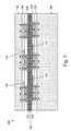
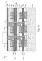
- FIGS. 1 through 16are a series of cross-sectional views illustrating a method of implementing three-dimensional integration of multiple integrated circuit (IC) devices, in accordance with an embodiment of the invention.
- the TSVsare formed post bonding.
- the actual bondinginvolves only oxide-to-oxide bonding (or more generally insulator-to-insulator bonding) of the wafers, in that because the TSVs are not formed on the individual wafers prior to bonding, there are no alignment issues therebetween with respect to the vias.
- the wafer 100represents a memory wafer having front-end-of-line (FEOL), middle-of-line (MOL), and back-end-of-line (BEOL) structures formed thereon, as known in the art.
- the exemplary memory wafer 100is shown having a thick sacrificial base layer 102 (e.g., a heavily doped P+ layer), and a lightly doped epitaxial layer 104 formed on the sacrificial base layer.
- the sacrificial base layer 102may have a dopant concentration of, for example, 1000 times that of the epi-layer 104 .
- the FEOL structuresare formed in the epi-layer 104 , which serves as the memory layer substrate. As indicated above, this layer 104 could be embodied by a bulk substrate of semiconducting material or a semiconductor-on-insulator (SOI) substrate.
- the wiring layers (e.g., 106 and 108 ) shown in the MOL and BEOL regions of the waferare illustrative only. In an actual device, there may be several layers of insulator materials and associated wiring formed therein. As also shown in FIG. 1( a ), one or more strap/landing pads 110 are formed in the wiring layers. For purposes of illustration, the pads are shown at the M 1 (first) level of wiring, although such pads can be formed at various levels within the device.
- the wafer 200represents a processor wafer having FEOL, MOL and BEOL structures formed thereon, as known in the art.
- the exemplary memory wafer 200is shown having a base substrate layer 202 (e.g., a P-type layer), which may be embodied by a bulk substrate of semiconducting material such as silicon or an SOI substrate.
- the wiring layerse.g., 206 and 208 ) shown in the MOL and BEOL regions of the wafer 200 are illustrative only.
- the processor wafer 200also includes metal strap/landing pads 210 formed in one or more of the wiring layers.
- FIGS. 2( a ) and 2 ( b )depict passivation of the wafers 100 , 200 , respectively, with an oxide layer 120 , 220 , or other suitable type of insulator material (including any adhesive material) in preparation of wafer bonding. Both passivated wafers 100 , 200 are then shown together in FIG. 3 where, in particular, memory wafer 100 is flipped and aligned with processor wafer 200 . Such alignment may be implemented through any known techniques such as, for example, infrared (IR) alignment or other suitable method. It will be noted that since no TSVs have been formed in either of the wafers 100 , 200 to this point, there is no need to align any conductor materials between the wafers.
- IRinfrared
- the wafers 100 , 200are bonded together to form an integrated wafer, now depicted generally at 300 .
- the bondingmay be, for example, oxide-to-oxide bonding (e.g., by annealing), oxide/adhesive bonding, or any other suitable technique known in the art that results in a strong bond between electrically insulating layers.
- integrated wafer 300has a bonding interface 302 between layers 120 and 220 , wherein the interface is comprised entirely of insulating materials, and no conducting materials such as vias.
- the exemplary wafers 100 , 200 that are bonded to form integrated wafer 300need not be the specific types of wafers presented in the above example.
- a processor wafercould also be “flipped” and bonded to a memory wafer.
- one memory wafercould be flipped and bonded in the above described manner to another memory wafer.
- the wafers 100 , 200may represent any type of integrated circuit device formed on a substrate where it is desired to integrate the same or other types of integrated circuit devices in a 3D fashion.
- FIG. 5illustrates the removal of the thick sacrificial base layer used in forming the memory portion of the wafer 300 .
- the removalmay be implemented by any suitable means in the semiconductor arts including, for example, techniques such as grinding, chemical mechanical polishing (CMP), etching, etc., as well as combinations thereof.
- CMPchemical mechanical polishing
- etchingbecomes one suitable technique for removal of the sacrificial base layer.
- the epitaxial layer 104 of the memory portion of the integrated wafer 300is now exposed for further processing.
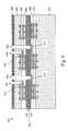
- the processing steps for the “via last” TSV formationare commenced. This may include, for example, forming a passivation layer 304 (e.g., an oxide) on the epitaxial layer 104 . Then, first and second sets of TSVs are defined by via patterning and etching. More specifically, a “shallow” set of TSVs 306 is formed through the passivation layer 304 , the epitaxial layer 104 , and one or more of the wiring layers 106 , 108 corresponding to the particular locations of the landing pads 110 of the memory portion of the wafer 300 .
- a passivation layer 304e.g., an oxide
- first and second sets of TSVsare defined by via patterning and etching. More specifically, a “shallow” set of TSVs 306 is formed through the passivation layer 304 , the epitaxial layer 104 , and one or more of the wiring layers 106 , 108 corresponding to the particular locations of the landing pads 110 of the memory portion
- a “deep” set of TSVs 308is formed through the entirety of the memory portion of the wafer 300 , as well as the passivation layers 120 and 220 , down to the landing pads 210 in the processor portion of the wafer 300 .
- the landing pads 210 in the processor portionmay also be located in various wiring levels, and thus the deep TSV etch may continue through one or more of the wiring layer 206 , 208 in the event the landing pads 210 are present at these levels.
- the shallow TSVs 306may have a diameter of about 2-3 microns ( ⁇ m), a total depth of about 8-15 ⁇ m, and a pitch (spacing) of about 10 ⁇ m or more.
- the deep TSVs 308may have a diameter of about 5-10 ⁇ m, a total depth of about 25-40 ⁇ m, and a pitch of about 10 ⁇ m or more.
- a via liner layere.g., tantalum, tantalum nitride, etc.
- metal seed layere.g., copper
- metal fill 310e.g., copper
- any connection straps desired between shallow and deep TSVsmay be formed such as shown in FIG. 8 .
- another passivation (e.g., oxide) layer 312is formed, followed by patterning etching, liner layer, seed layer, metal plating and CMP to form a connection strap 314 between a shallow/deep TSV pair.
- etchinge.g., oxide
- liner layere.g., seed layer
- metal plating and CMPe.g., CMP
- a top passivation layer(not shown), patterning the passivation layer and forming a conductive capture pad (not shown) or other metallurgy for an external connection such as a C 4 solder ball.
- a conductive capture pad(not shown) or other metallurgy for an external connection such as a C 4 solder ball.
- FIG. 9another layer 320 of passivation is formed on the wafer.
- Layer 320may be, for example, an oxide layer such as used for layers 120 , 220 , or other suitable type of insulator material including any adhesive material in preparation of wafer bonding.
- FIG. 10illustrates the alignment of a second memory wafer 400 with the integrated wafer 300 .
- the second memory wafer 400is similar in construction with respect to the first memory wafer 100 shown in FIG. 3 , in that the wafer 400 includes a thick sacrificial base layer 402 (e.g., a heavily doped P+ layer), a lightly doped epitaxial layer 404 formed on the sacrificial base layer 402 , one or more wiring layers 406 , 408 in the MOL and BEOL regions, and one or more strap/landing pads 410 formed in the wiring layers.
- the wafers 300 and 400are bonded together to form a single integrated wafer, now depicted generally at 500 .
- the bondingmay be, for example, oxide-to-oxide bonding (e.g., by annealing), oxide/adhesive bonding, or any other suitable technique known in the art that results in a strong bond between electrically insulating layers.
- integrated wafer 500has a second bonding interface 502 between layers 320 and 520 , wherein (like the first bonding interface 302 ) the second bonding interface 502 is comprised entirely of insulating materials, and no conducting materials such as vias.
- FIG. 12the thick sacrificial base layer 402 used in forming the second memory wafer 400 is removed by any suitable means in the semiconductor arts such as grinding, CMP, etching, etc.
- the epitaxial layer 404 of the second memory portion of the integrated wafer 500is now exposed for further processing.
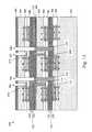
- FIG. 13then illustrates the formation of another set of TSVs, including forming a passivation layer 504 (e.g., an oxide) on the epitaxial layer 404 .
- a passivation layer 504e.g., an oxide
- a shallow set of TSVs 506is formed through the passivation layer 504 , the epitaxial layer 404 , and one or more of the wiring layers 406 , 408 corresponding to the particular locations of the landing pads 410 of the second memory portion of the wafer 500 .
- a deep set of TSVs 508is formed through the entirety of the second memory portion of the wafer 500 , as well as the passivation layers 420 and 320 .
- one of the deep TSVs 508lands on the strap 314 that connects circuitry between the processor and first memory portions of the wafer 500 .
- Another of the deep TSVs 508is shown to connect to an earlier formed TSV, thereby extending the total depth of the TSV 508 from the top of the device down to the landing strap 210 in the processor portion.
- an oxide lineris formed on sidewalls thereof in order to prevent subsequent diffusion of the conductive via fill materials.
- the deposition of the thin oxide lineris then followed up by an anisotropic etch to remove the liner from the horizontal surfaces.
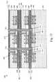
- standard processingmay be carried out to form a via liner layer (e.g., tantalum, tantalum nitride, etc.), metal seed layer, and metal fill 510 (e.g., copper), after which the excess material is planarized such as by CMP, as shown in FIG. 14 .
- connection straps between shallow and deep TSVsare formed.
- connection straps 514between the shallow/deep TSV pair.
- another passivation (e.g., oxide) layer 512is formed, followed by patterning etching, liner layer, seed layer, metal plating and CMP to form connection straps 514 between the shallow/deep TSV pair.
- dual damascene processingcan also be used to simultaneously define and fill the via and strap structures.
- FIG. 16depicts a capture pad 516 (e.g., C 4 ) formed atop the wafer 500 for providing external electrical contact for the 3D integrated wafer 500 .
- the capture pad 516may be formed with or without another passivation layer (not shown).
- additional wafer layermay also be stacked and bonded, in the manner described above, prior to a “via last” definition that electrically interconnects the bonded wafers.
- all bonding processesare, in essence, insulator-to-insulator in that no alignment/bonding of conductive structures need take place for the integration. It is noted that although the deep TSVs ultimately pass through a wafer bonding interface, the vias themselves do not comprise a part of that interface since the metal fill takes place post-bonding.
- the exemplary process flow described hereinmay have many variations including, but not limited to, the use of straight, “via only” wafers, wafers with only wiring redistribution and wafer connection TSVs, and wafers having specific features such as capacitors, voltage regulator modules (VRMs), etc.
- the various waferse.g., processors, wafers
- BOXburied oxide
Landscapes
- Engineering & Computer Science (AREA)
- Microelectronics & Electronic Packaging (AREA)
- Power Engineering (AREA)
- Computer Hardware Design (AREA)
- Physics & Mathematics (AREA)
- Condensed Matter Physics & Semiconductors (AREA)
- General Physics & Mathematics (AREA)
- Manufacturing & Machinery (AREA)
- Internal Circuitry In Semiconductor Integrated Circuit Devices (AREA)
Abstract
Description
- The present invention relates generally to semiconductor device manufacturing techniques and, more particularly, to implementing three-dimensional integration of multiple integrated circuit (IC) devices.
- The packaging density in electronic industry continuously increases in order to accommodate more electronic devices into a package. In this regard, three-dimensional (3D) wafer-to-wafer stacking technology substantially contributes to the device integration process. Typically, a semiconductor wafer includes several layers of integrated circuitry (e.g., processors, programmable devices, memory devices, etc.) built on a silicon substrate. A top layer of the wafer may be connected to a bottom layer of the wafer through silicon interconnects or vias. In order to form a 3D wafer stack, two or more wafers are placed on top of one other and bonded.
- 3D wafer stacking technology offers a number of potential benefits, including, for example, improved form factors, lower costs, enhanced performance, and greater integration through system-on-chip (SOC) solutions. In addition, the 3D wafer stacking technology may provide other functionality to the chip. For instance, after being formed, the 3D wafer stack may be diced into stacked dies or chips, with each stacked chip having multiple tiers (i.e., layers) of integrated circuitry. SOC architectures formed by 3D wafer stacking can enable high bandwidth connectivity of products such as, for example, logic circuitry and dynamic random access memory (DRAM), that otherwise have incompatible process flows. At present, there are many applications for 3D wafer stacking technology, including high performance processing devices, video and graphics processors, high density and high bandwidth memory chips, and other SOC solutions.
- In an exemplary embodiment, a method of implementing three-dimensional (3D) integration of multiple integrated circuit (IC) devices includes forming a first insulating layer over a first IC device; forming a second insulating layer over a second IC device; forming a 3D, bonded IC device by aligning and bonding the first insulating layer of the first IC device to the second insulating layer of the second IC device so as to define a bonding interface therebetween, wherein the bonding interface is absent of electrically conductive materials; subsequent to the bonding, defining a first set of vias within the 3D bonded IC device, the first set of vias landing on conductive pads located within the first IC device, and defining a second set of vias within the 3D bonded IC device, the second set of vias landing on conductive pads located within the second device, such that the second set of vias passes through the bonding interface; and filling the first and second sets of vias with a conductive material, and electrically connecting at least one via of the first set of vias to at least one via of the second set of vias, thereby establishing electrical communication between the first and second ICs of the 3D bonded IC device.
- In another embodiment, a method of implementing three-dimensional (3D) integration of multiple integrated circuit (IC) devices includes forming a first IC device having a semiconductor substrate, front-end-of-line (FEOL) structures, middle-of-line (MOL) structures, and back-end-of-line (BEOL) structures, with a first insulating layer over the BEOL structures of the first IC device; forming a second IC device having a semiconductor substrate, FEOL structures, MOL structures, and BEOL structures, with a second insulating layer over the BEOL structures of the second IC device; forming a 3D, bonded IC device by aligning and bonding the first insulating layer of the first IC device to the second insulating layer of the second IC device so as to define a first bonding interface therebetween, wherein the first bonding interface is absent of electrically conductive materials; subsequent to the bonding, defining a first set of vias within the 3D bonded IC device, the first set of vias landing on conductive pads located within the first IC device, and defining a second set of vias within the 3D bonded IC device, the second set of vias landing on conductive pads located within the second device, such that the second set of vias passes through the first bonding interface; and filling the first and second sets of vias with a conductive material, and electrically connecting at least one via of the first set of vias to at least one via of the second set of vias, thereby establishing electrical communication between the first and second ICs of the 3D bonded IC device.
- In another embodiment, a three-dimensional (3D) integrated circuit (IC) device includes a first IC device bonded to a second IC device at a first bonding interface therebetween, thereby defining a 3D, bonded IC device, the first bonding interface defined between a first insulating layer of the first IC device and second insulating layer of the second IC device, wherein the first bonding interface is absent of electrically conductive materials; a first set of vias defined within the 3D bonded IC device, the first set of vias landing on conductive pads located within the first IC device, and a second set of vias defined within the 3D bonded IC device, the second set of vias landing on conductive pads located within the second device, such that the second set of vias passes through the first bonding interface; and the first and second sets of vias filled with a conductive material, and electrically connecting at least one via of the first set of vias to at least one via of the second set of vias, thereby establishing electrical communication between the first and second ICs of the 3D bonded IC device.
- Referring to the exemplary drawings wherein like elements are numbered alike in the several Figures:
FIGS. 1 through 16 are a series of cross-sectional views illustrating a method of implementing three-dimensional integration of multiple integrated circuit (IC) devices, in accordance with an embodiment of the invention.- One disadvantage associated with the current 3D wafer stacking technology concerns the use of adhesives to bond the wafers. Such adhesives limit the amount of practical, in-fab processing and raised reliability concerns due to undesirable inherent polymeric adhesive properties, such as thermal stability. In addition, achieving acceptable alignment of pre-existing through silicon vias (TSV) across the entire diameter of a pair of wafers is also difficult, which also creates reliability concerns.
- Accordingly, disclosed herein is a method and resulting structure for 3D wafer integration bonding in which the TSVs are formed post bonding. In this manner, the actual bonding involves only oxide-to-oxide bonding (or more generally insulator-to-insulator bonding) of the wafers, in that because the TSVs are not formed on the individual wafers prior to bonding, there are no alignment issues therebetween with respect to the vias.
- It should be appreciated that although specific wafer substrate bonding process flows are depicted herein, such descriptions are exemplary only, and that the principles disclosed herein are also applicable to various types of TSV conductive materials, dielectric and adhesive interface materials, and multiple types of semiconductor wafers and substrates.
- Referring initially to
FIG. 1( a), there is shown a cross-sectional view of afirst wafer 100 to be integrated and bonded with one or more additional wafers. In the exemplary embodiment depicted, thewafer 100 represents a memory wafer having front-end-of-line (FEOL), middle-of-line (MOL), and back-end-of-line (BEOL) structures formed thereon, as known in the art. In addition, theexemplary memory wafer 100 is shown having a thick sacrificial base layer102 (e.g., a heavily doped P+ layer), and a lightly dopedepitaxial layer 104 formed on the sacrificial base layer. Thesacrificial base layer 102 may have a dopant concentration of, for example, 1000 times that of the epi-layer 104. The FEOL structures are formed in the epi-layer 104, which serves as the memory layer substrate. As indicated above, thislayer 104 could be embodied by a bulk substrate of semiconducting material or a semiconductor-on-insulator (SOI) substrate. - As will be appreciated, the wiring layers (e.g.,106 and108) shown in the MOL and BEOL regions of the wafer are illustrative only. In an actual device, there may be several layers of insulator materials and associated wiring formed therein. As also shown in
FIG. 1( a), one or more strap/landing pads 110 are formed in the wiring layers. For purposes of illustration, the pads are shown at the M1 (first) level of wiring, although such pads can be formed at various levels within the device. - Referring now to
FIG. 1( b), there is shown a cross-sectional view of asecond wafer 200 to be integrated and bonded with thefirst wafer 100 shown inFIG. 1( a). In the exemplary embodiment depicted, thewafer 200 represents a processor wafer having FEOL, MOL and BEOL structures formed thereon, as known in the art. In addition, theexemplary memory wafer 200 is shown having a base substrate layer202 (e.g., a P-type layer), which may be embodied by a bulk substrate of semiconducting material such as silicon or an SOI substrate. Again, the wiring layers (e.g.,206 and208) shown in the MOL and BEOL regions of thewafer 200 are illustrative only. As is the case with thememory wafer 100, theprocessor wafer 200 also includes metal strap/landing pads 210 formed in one or more of the wiring layers. FIGS. 2( a) and2(b) depict passivation of thewafers oxide layer wafers FIG. 3 where, in particular,memory wafer 100 is flipped and aligned withprocessor wafer 200. Such alignment may be implemented through any known techniques such as, for example, infrared (IR) alignment or other suitable method. It will be noted that since no TSVs have been formed in either of thewafers - As then shown in
FIG. 4 , thewafers wafer 300 has abonding interface 302 betweenlayers - It should be appreciated at this point that the
exemplary wafers wafer 300 need not be the specific types of wafers presented in the above example. For instance, a processor wafer could also be “flipped” and bonded to a memory wafer. In addition, one memory wafer could be flipped and bonded in the above described manner to another memory wafer. Even more generally, thewafers - In any case,
FIG. 5 illustrates the removal of the thick sacrificial base layer used in forming the memory portion of thewafer 300. The removal may be implemented by any suitable means in the semiconductor arts including, for example, techniques such as grinding, chemical mechanical polishing (CMP), etching, etc., as well as combinations thereof. By doping the sacrificial base layer at such a heavy concentration with respect to theepitaxial layer 104, a strong etch selectivity between the two layers results. Thus, etching becomes one suitable technique for removal of the sacrificial base layer. Upon removal of the sacrificial base layer, theepitaxial layer 104 of the memory portion of the integratedwafer 300 is now exposed for further processing. - Referring now to
FIG. 6 , the processing steps for the “via last” TSV formation are commenced. This may include, for example, forming a passivation layer304 (e.g., an oxide) on theepitaxial layer 104. Then, first and second sets of TSVs are defined by via patterning and etching. More specifically, a “shallow” set ofTSVs 306 is formed through thepassivation layer 304, theepitaxial layer 104, and one or more of thewiring layers landing pads 110 of the memory portion of thewafer 300. In addition, a “deep” set of TSVs308 is formed through the entirety of the memory portion of thewafer 300, as well as thepassivation layers landing pads 210 in the processor portion of thewafer 300. As is the case with thelanding pads 110 in the memory portion, thelanding pads 210 in the processor portion may also be located in various wiring levels, and thus the deep TSV etch may continue through one or more of thewiring layer landing pads 210 are present at these levels. - In an exemplary embodiment, the
shallow TSVs 306 may have a diameter of about 2-3 microns (μm), a total depth of about 8-15 μm, and a pitch (spacing) of about 10 μm or more. Thedeep TSVs 308 may have a diameter of about 5-10 μm, a total depth of about 25-40 μm, and a pitch of about 10 μm or more. After the initial etch of both sets of the TSVs, an oxide liner is formed on sidewalls thereof in order to prevent subsequent diffusion of the conductive via fill materials. The deposition of a thin oxide liner is then followed up by an anisotropic etch to remove the liner from the horizontal surfaces, such as themetallic landing pads FIG. 7 . - At this point in the process, any connection straps desired between shallow and deep TSVs (thereby defining electrical communication between the processor and memory portions of the integrated wafer300) may be formed such as shown in
FIG. 8 . As is shown, another passivation (e.g., oxide)layer 312 is formed, followed by patterning etching, liner layer, seed layer, metal plating and CMP to form aconnection strap 314 between a shallow/deep TSV pair. Although the embodiment depicted is an example of single damascene processing, it will be understood that dual damascene processing can also be used to simultaneously define and fill the via and strap structures. - In the event the resulting 3D integrated structure were substantially complete at this point, final processing steps would then be implemented, such as forming a top passivation layer (not shown), patterning the passivation layer and forming a conductive capture pad (not shown) or other metallurgy for an external connection such as a C4 solder ball. However, for purposes of illustration, it will be assumed that further 3D wafer integration is desired, such as (for example) the addition of more memory chips. Accordingly, as shown in
FIG. 9 , anotherlayer 320 of passivation is formed on the wafer.Layer 320 may be, for example, an oxide layer such as used forlayers FIG. 10 illustrates the alignment of asecond memory wafer 400 with theintegrated wafer 300. Thesecond memory wafer 400 is similar in construction with respect to thefirst memory wafer 100 shown inFIG. 3 , in that thewafer 400 includes a thick sacrificial base layer402 (e.g., a heavily doped P+ layer), a lightly dopedepitaxial layer 404 formed on thesacrificial base layer 402, one or more wiring layers406,408 in the MOL and BEOL regions, and one or more strap/landing pads 410 formed in the wiring layers. As then shown inFIG. 11 , thewafers integrated wafer 500 has asecond bonding interface 502 betweenlayers 320 and520, wherein (like the first bonding interface302) thesecond bonding interface 502 is comprised entirely of insulating materials, and no conducting materials such as vias.- The next steps in the processing sequence are similar to that shown in
FIGS. 5-8 . For example, inFIG. 12 , the thicksacrificial base layer 402 used in forming thesecond memory wafer 400 is removed by any suitable means in the semiconductor arts such as grinding, CMP, etching, etc. Upon removal of the sacrificial base layer, theepitaxial layer 404 of the second memory portion of theintegrated wafer 500 is now exposed for further processing.FIG. 13 then illustrates the formation of another set of TSVs, including forming a passivation layer504 (e.g., an oxide) on theepitaxial layer 404. Once again, a shallow set ofTSVs 506 is formed through thepassivation layer 504, theepitaxial layer 404, and one or more of the wiring layers406,408 corresponding to the particular locations of thelanding pads 410 of the second memory portion of thewafer 500. In addition, a deep set ofTSVs 508 is formed through the entirety of the second memory portion of thewafer 500, as well as the passivation layers420 and320. In the exemplary embodiment depicted, one of thedeep TSVs 508 lands on thestrap 314 that connects circuitry between the processor and first memory portions of thewafer 500. Another of thedeep TSVs 508 is shown to connect to an earlier formed TSV, thereby extending the total depth of theTSV 508 from the top of the device down to thelanding strap 210 in the processor portion. - After the etch of both sets of the
TSVs FIG. 14 . InFIG. 15 , connection straps between shallow and deep TSVs are formed. In particular, another passivation (e.g., oxide)layer 512 is formed, followed by patterning etching, liner layer, seed layer, metal plating and CMP to form connection straps514 between the shallow/deep TSV pair. Again, although the illustrated embodiment is an example of single damascene processing, it will be understood that dual damascene processing can also be used to simultaneously define and fill the via and strap structures. - Finally,
FIG. 16 depicts a capture pad516 (e.g., C4) formed atop thewafer 500 for providing external electrical contact for the 3D integratedwafer 500. Thecapture pad 516 may be formed with or without another passivation layer (not shown). Again, prior to formation of any external capture pads, additional wafer layer may also be stacked and bonded, in the manner described above, prior to a “via last” definition that electrically interconnects the bonded wafers. In so doing, all bonding processes are, in essence, insulator-to-insulator in that no alignment/bonding of conductive structures need take place for the integration. It is noted that although the deep TSVs ultimately pass through a wafer bonding interface, the vias themselves do not comprise a part of that interface since the metal fill takes place post-bonding. - It should be understood that the exemplary process flow described herein may have many variations including, but not limited to, the use of straight, “via only” wafers, wafers with only wiring redistribution and wafer connection TSVs, and wafers having specific features such as capacitors, voltage regulator modules (VRMs), etc. In addition, the various wafers (e.g., processors, wafers) may also include buried oxide (BOX) layers therein for SOI applications.
- While the invention has been described with reference to a preferred embodiment or embodiments, it will be understood by those skilled in the art that various changes may be made and equivalents may be substituted for elements thereof without departing from the scope of the invention. In addition, many modifications may be made to adapt a particular situation or material to the teachings of the invention without departing from the essential scope thereof. Therefore, it is intended that the invention not be limited to the particular embodiment disclosed as the best mode contemplated for carrying out this invention, but that the invention will include all embodiments falling within the scope of the appended claims.
Claims (27)
1. A method of implementing three-dimensional (3D) integration of multiple integrated circuit (IC) devices, the method comprising:
forming a first insulating layer over a first IC device;
forming a second insulating layer over a second IC device;
forming a 3D, bonded IC device by aligning and bonding the first insulating layer of the first IC device to the second insulating layer of the second IC device so as to define a first bonding interface therebetween, wherein the first bonding interface is absent of electrically conductive materials;
subsequent to the bonding, defining a first set of vias within the 3D bonded IC device, the first set of vias landing on conductive pads located within the first IC device, and defining a second set of vias within the 3D bonded IC device, the second set of vias landing on conductive pads located within the second device, such that the second set of vias passes through the first bonding interface; and
filling the first and second sets of vias with a conductive material, and electrically connecting at least one via of the first set of vias to at least one via of the second set of vias, thereby establishing electrical communication between the first and second ICs of the 3D bonded IC device.
2. The method ofclaim 1 , further comprising:
forming a third insulating layer over the 3D bonded IC device;
forming a fourth insulating layer over a third IC device;
attaching the third IC device to the 3D bonded IC device by aligning and bonding the fourth insulating layer of the third IC device to the third insulating layer of the 3D bonded IC device so as to define a second bonding interface therebetween, wherein the second bonding interface is absent of electrically conductive materials;
defining a third set of vias within the 3D bonded IC device, the third set of vias landing on conductive pads located within the third IC device, and defining a fourth set of vias within the 3D bonded IC device, the fourth set of vias landing on one or more of the second set of vias within the 3D bonded IC device and electrical connections between the first and second sets of vias within the 3D bonded IC device, such that the fourth set of vias passes through the second bonding interface; and
filling the third and fourth sets of vias with a conductive material, and electrically connecting at least one via of the third set of vias to at least one via of the fourth set of vias, thereby establishing electrical communication between the first, second and third ICs of the 3D bonded IC device.
3. The method ofclaim 1 , wherein the first IC device comprises an epitaxially grown semiconductor layer formed on a sacrificial base layer, and wherein the sacrificial base layer is removed subsequent to bonding the first and second IC devices, and prior to formation of the first and second sets of vias.
4. The method ofclaim 2 , wherein the sacrificial base layer of the first IC device has a substantially higher dopant concentration with respect to the epitaxially grown semiconductor layer so as to create an etch selectivity therebetween.
5. The method ofclaim 1 , wherein the first and second insulating layers comprise oxide layers, and the bonding comprises one or more of oxide-to-oxide bonding and oxide/adhesive bonding.
6. The method ofclaim 1 , further comprising forming an oxide liner over the first and second sets of vias after etching thereof and removing portions of the oxide liner on horizontal surfaces of the 3D bonded IC device prior to filling the first and second sets of vias with the conductive material.
7. The method ofclaim 1 , wherein vias of the second set of vias are deeper than vias of the first set of vias.
8. The method ofclaim 7 , wherein vias of the second set of vias have a larger diameter than vias of the first set of vias.
9. The method ofclaim 1 , wherein the first IC device comprises a memory device and the second IC device comprises a processor device.
10. The method ofclaim 2 , wherein the first IC device comprises a memory device, the second IC device comprises a processor device, and the third IC device comprises another memory device.
11. A method of implementing three-dimensional (3D) integration of multiple integrated circuit (IC) devices, the method comprising:
forming a first IC device having a semiconductor substrate, front-end-of-line (FEOL) structures, middle-of-line (MOL) structures, and back-end-of-line (BEOL) structures, with a first insulating layer over the BEOL structures of the first IC device;
forming a second IC device having a semiconductor substrate, FEOL structures, MOL structures, and BEOL structures, with a second insulating layer over the BEOL structures of the second IC device;
forming a 3D, bonded IC device by aligning and bonding the first insulating layer of the first IC device to the second insulating layer of the second IC device so as to define a first bonding interface therebetween, wherein the first bonding interface is absent of electrically conductive materials;
subsequent to the bonding, defining a first set of vias within the 3D bonded IC device, the first set of vias landing on conductive pads located within the first IC device, and defining a second set of vias within the 3D bonded IC device, the second set of vias landing on conductive pads located within the second device, such that the second set of vias passes through the first bonding interface; and
filling the first and second sets of vias with a conductive material, and electrically connecting at least one via of the first set of vias to at least one via of the second set of vias, thereby establishing electrical communication between the first and second ICs of the 3D bonded IC device.
12. The method ofclaim 11 , further comprising:
forming a third insulating layer over the 3D bonded IC device;
forming a third IC device having a semiconductor substrate, FEOL structures, MOL structures, and BEOL structures, with a fourth insulating layer over the BEOL structures of the third IC device;
attaching the third IC device to the 3D bonded IC device by aligning and bonding the fourth insulating layer of the third IC device to the third insulating layer of the 3D bonded IC device so as to define a second bonding interface therebetween, wherein the second bonding interface is absent of electrically conductive materials;
defining a third set of vias within the 3D bonded IC device, the third set of vias landing on conductive pads located within the third IC device, and defining a fourth set of vias within the 3D bonded IC device, the fourth set of vias landing on one or more of the second set of vias within the 3D bonded IC device and electrical connections between the first and second sets of vias within the 3D bonded IC device, such that the fourth set of vias passes through the second bonding interface; and
filling the third and fourth sets of vias with a conductive material, and electrically connecting at least one via of the third set of vias to at least one via of the fourth set of vias, thereby establishing electrical communication between the first, second and third ICs of the 3D bonded IC device.
13. The method ofclaim 11 , wherein the forming the first IC device comprises epitaxially growing the semiconductor layer thereof on a sacrificial base layer, and wherein removing the sacrificial base layer subsequent to bonding the first and second IC devices, and prior to formation of the first and second sets of vias.
14. The method ofclaim 12 , wherein the sacrificial base layer of the first IC device has a substantially higher dopant concentration with respect to the epitaxially grown semiconductor layer so as to create an etch selectivity therebetween.
15. The method ofclaim 11 , wherein the first and second insulating layers comprise oxide layers, and the bonding comprises one or more of oxide-to-oxide bonding and oxide/adhesive bonding.
16. The method ofclaim 11 , further comprising forming an oxide liner over the first and second sets of vias after etching thereof and removing portions of the oxide liner on horizontal surfaces of the 3D bonded IC device prior to filling the first and second sets of vias with the conductive material.
17. The method ofclaim 11 , wherein vias of the second set of vias are deeper than vias of the first set of vias.
18. The method ofclaim 17 , wherein vias of the second set of vias have a larger diameter than vias of the first set of vias.
19. The method ofclaim 11 , wherein the first IC device comprises a memory device and the second IC device comprises a processor device.
20. The method ofclaim 12 , wherein the first IC device comprises a memory device, the second IC device comprises a processor device, and the third IC device comprises another memory device.
21. A three-dimensional (3D) integrated circuit (IC) device, comprising:
a first IC device bonded to a second IC device at a first bonding interface therebetween, thereby defining a 3D, bonded IC device, the first bonding interface defined between a first insulating layer of the first IC device and second insulating layer of the second IC device, wherein the first bonding interface is absent of electrically conductive materials;
a first set of vias defined within the 3D bonded IC device, the first set of vias landing on conductive pads located within the first IC device, and a second set of vias defined within the 3D bonded IC device, the second set of vias landing on conductive pads located within the second device, such that the second set of vias passes through the first bonding interface; and
the first and second sets of vias filled with a conductive material, and electrically connecting at least one via of the first set of vias to at least one via of the second set of vias, thereby establishing electrical communication between the first and second ICs of the 3D bonded IC device.
22. The device ofclaim 21 , further comprising:
a third IC device attached to the 3D bonded IC device at a second bonding interface therebetween, the second bonding interface defined between a third insulating layer formed over the 3D bonded IC device and a fourth insulating layer formed of the third IC device;
a third set of vias defined within the 3D bonded IC device, the third set of vias landing on conductive pads located within the third IC device, and a fourth set of vias defined within the 3D bonded IC device, the fourth set of vias landing on one or more of the second set of vias within the 3D bonded IC device;
electrical connections between the first and second sets of vias within the 3D bonded IC device, such that the fourth set of vias passes through the second bonding interface; and
the third and fourth sets of vias filled with a conductive material, and electrically connecting at least one via of the third set of vias to at least one via of the fourth set of vias, thereby establishing electrical communication between the first, second and third ICs of the 3D bonded IC device.
23. The device ofclaim 21 , wherein the first and second insulating layers comprise oxide layers.
24. The device ofclaim 21 , wherein vias of the second set of vias are deeper than vias of the first set of vias.
25. The device ofclaim 24 , wherein vias of the second set of vias have a larger diameter than vias of the first set of vias.
26. The device ofclaim 1 , wherein the first IC device comprises a memory device and the second IC device comprises a processor device.
27. The device ofclaim 22 , wherein the first IC device comprises a memory device, the second IC device comprises a processor device, and the third IC device comprises another memory device.
Priority Applications (4)
| Application Number | Priority Date | Filing Date | Title |
|---|---|---|---|
| US12/426,466US9406561B2 (en) | 2009-04-20 | 2009-04-20 | Three dimensional integrated circuit integration using dielectric bonding first and through via formation last |
| EP10767507.6AEP2422366A4 (en) | 2009-04-20 | 2010-04-08 | Three dimensional integrated circuit integration using dielectric bonding first and through via formation last |
| CN2010800103402ACN102341907A (en) | 2009-04-20 | 2010-04-08 | Three dimensional integrated circuit integration using dielectric bonding first and through via formation last |
| PCT/US2010/030357WO2010123691A1 (en) | 2009-04-20 | 2010-04-08 | Three dimensional integrated circuit integration using dielectric bonding first and through via formation last |
Applications Claiming Priority (1)
| Application Number | Priority Date | Filing Date | Title |
|---|---|---|---|
| US12/426,466US9406561B2 (en) | 2009-04-20 | 2009-04-20 | Three dimensional integrated circuit integration using dielectric bonding first and through via formation last |
Publications (2)
| Publication Number | Publication Date |
|---|---|
| US20100264551A1true US20100264551A1 (en) | 2010-10-21 |
| US9406561B2 US9406561B2 (en) | 2016-08-02 |
Family
ID=42980379
Family Applications (1)
| Application Number | Title | Priority Date | Filing Date |
|---|---|---|---|
| US12/426,466Active2030-10-27US9406561B2 (en) | 2009-04-20 | 2009-04-20 | Three dimensional integrated circuit integration using dielectric bonding first and through via formation last |
Country Status (4)
| Country | Link |
|---|---|
| US (1) | US9406561B2 (en) |
| EP (1) | EP2422366A4 (en) |
| CN (1) | CN102341907A (en) |
| WO (1) | WO2010123691A1 (en) |
Cited By (210)
| Publication number | Priority date | Publication date | Assignee | Title |
|---|---|---|---|---|
| US20100140808A1 (en)* | 2007-10-30 | 2010-06-10 | International Business Machines Corporation | Power Distribution In A Vertically Integrated Circuit |
| US20110034021A1 (en)* | 2009-01-22 | 2011-02-10 | International Business Machines Corporation | Programmable through silicon via |
| US20110189820A1 (en)* | 2010-02-04 | 2011-08-04 | Headway Technologies, Inc. | Method of manufacturing layered chip package |
| US20110193199A1 (en)* | 2010-02-09 | 2011-08-11 | International Business Machines Corporation | Electromigration immune through-substrate vias |
| US20120112358A1 (en)* | 2010-11-10 | 2012-05-10 | Institute of Microelectronics, Chinese Academy of Sciences | Stack-type semiconductor device and method for manufacturing the same |
| CN102468284A (en)* | 2010-11-10 | 2012-05-23 | 中国科学院微电子研究所 | Stacked semiconductor device and manufacturing method thereof |
| US8530973B2 (en) | 2008-08-27 | 2013-09-10 | Semiconductor Energy Laboratory Co., Ltd. | Method for manufacturing semiconductor device |
| US8546961B2 (en) | 2011-01-10 | 2013-10-01 | International Business Machines Corporation | Alignment marks to enable 3D integration |
| US8563403B1 (en) | 2012-06-27 | 2013-10-22 | International Business Machines Corporation | Three dimensional integrated circuit integration using alignment via/dielectric bonding first and through via formation last |
| US8592952B2 (en) | 2010-05-31 | 2013-11-26 | SK Hynix Inc. | Semiconductor chip and semiconductor package with stack chip structure |
| US20140080245A1 (en)* | 2011-07-05 | 2014-03-20 | United Microelectronics Corporation | Method for fabricating optical micro structure and applications thereof |
| US20150187733A1 (en)* | 2013-12-27 | 2015-07-02 | International Business Machines Corporation | Combination of tsv and back side wiring in 3d integration |
| US20150264809A1 (en)* | 2014-03-11 | 2015-09-17 | Kabushiki Kaisha Toshiba | Wiring substrate and semiconductor device using the same |
| US20150270172A1 (en)* | 2011-01-29 | 2015-09-24 | International Business Machines Corporation | Novel 3D Integration Method using SOI Substrates and Structures Produced Thereby |
| US20150364401A1 (en)* | 2013-12-30 | 2015-12-17 | International Business Machines Corporation | Double-sided segmented line architecture in 3d integration |
| US20160181228A1 (en)* | 2013-09-17 | 2016-06-23 | Panasonic Intellectual Property Management Co., Ltd. | Semiconductor device and method for manufacturing same |
| US9406561B2 (en) | 2009-04-20 | 2016-08-02 | International Business Machines Corporation | Three dimensional integrated circuit integration using dielectric bonding first and through via formation last |
| US9496255B2 (en) | 2011-11-16 | 2016-11-15 | Qualcomm Incorporated | Stacked CMOS chipset having an insulating layer and a secondary layer and method of forming same |
| CN106158853A (en)* | 2015-04-24 | 2016-11-23 | 中国科学院微电子研究所 | Integrated circuit structure, manufacturing method thereof and semiconductor device |
| TWI585898B (en)* | 2015-08-31 | 2017-06-01 | 台灣積體電路製造股份有限公司 | Three-dimensional integrated circuit and manufacturing method thereof |
| US20170317011A1 (en)* | 2010-04-28 | 2017-11-02 | Taiwan Semiconductor Manufacturing Company, Ltd. | Through-Substrate Vias with Improved Connections |
| US20180025970A1 (en)* | 2016-07-25 | 2018-01-25 | Taiwan Semiconductor Manufacturing Co., Ltd. | Integrated circuit (ic) structure for high performance and functional density |
| US9881896B2 (en) | 2015-12-17 | 2018-01-30 | International Business Machines Corporation | Advanced chip to wafer stacking |
| US20180076260A1 (en)* | 2016-09-13 | 2018-03-15 | Imec Vzw | Sequential Integration Process |
| US9929050B2 (en)* | 2013-07-16 | 2018-03-27 | Taiwan Semiconductor Manufacturing Company, Ltd. | Mechanisms for forming three-dimensional integrated circuit (3DIC) stacking structure |
| US10127344B2 (en) | 2013-04-15 | 2018-11-13 | Monolithic 3D Inc. | Automation for monolithic 3D devices |
| US10163864B1 (en) | 2017-08-16 | 2018-12-25 | Globalfoundries Inc. | Vertically stacked wafers and methods of forming same |
| US10224279B2 (en) | 2013-03-15 | 2019-03-05 | Monolithic 3D Inc. | Semiconductor device and structure |
| US20190148435A1 (en)* | 2013-03-13 | 2019-05-16 | Taiwan Semiconductor Manufacturing Company, Ltd. | Interconnect Apparatus and Method |
| US10297586B2 (en) | 2015-03-09 | 2019-05-21 | Monolithic 3D Inc. | Methods for processing a 3D semiconductor device |
| US10325849B2 (en) | 2013-11-18 | 2019-06-18 | Taiwan Semiconductor Manufacturing Co., Ltd. | Different scaling ratio in FEOL/ MOL/ BEOL |
| US10325651B2 (en) | 2013-03-11 | 2019-06-18 | Monolithic 3D Inc. | 3D semiconductor device with stacked memory |
| US10366970B2 (en) | 2009-10-12 | 2019-07-30 | Monolithic 3D Inc. | 3D semiconductor device and structure |
| US10381328B2 (en) | 2015-04-19 | 2019-08-13 | Monolithic 3D Inc. | Semiconductor device and structure |
| US10388863B2 (en) | 2009-10-12 | 2019-08-20 | Monolithic 3D Inc. | 3D memory device and structure |
| US10418369B2 (en) | 2015-10-24 | 2019-09-17 | Monolithic 3D Inc. | Multi-level semiconductor memory device and structure |
| US10497713B2 (en) | 2010-11-18 | 2019-12-03 | Monolithic 3D Inc. | 3D semiconductor memory device and structure |
| US10515981B2 (en) | 2015-09-21 | 2019-12-24 | Monolithic 3D Inc. | Multilevel semiconductor device and structure with memory |
| JP2019220244A (en)* | 2018-06-18 | 2019-12-26 | インテル・コーポレーション | Three-dimensional (3D) flash memory with shared control circuit using wafer-to-wafer bonding |
| US10522225B1 (en) | 2015-10-02 | 2019-12-31 | Monolithic 3D Inc. | Semiconductor device with non-volatile memory |
| US20200083196A1 (en)* | 2012-12-22 | 2020-03-12 | Monolithic 3D Inc. | Method to form a 3d semiconductor device and structure |
| US10600888B2 (en) | 2012-04-09 | 2020-03-24 | Monolithic 3D Inc. | 3D semiconductor device |
| US10600657B2 (en) | 2012-12-29 | 2020-03-24 | Monolithic 3D Inc | 3D semiconductor device and structure |
| US10651054B2 (en) | 2012-12-29 | 2020-05-12 | Monolithic 3D Inc. | 3D semiconductor device and structure |
| US10679977B2 (en) | 2010-10-13 | 2020-06-09 | Monolithic 3D Inc. | 3D microdisplay device and structure |
| US10825779B2 (en) | 2015-04-19 | 2020-11-03 | Monolithic 3D Inc. | 3D semiconductor device and structure |
| US10833108B2 (en) | 2010-10-13 | 2020-11-10 | Monolithic 3D Inc. | 3D microdisplay device and structure |
| US10840239B2 (en) | 2014-08-26 | 2020-11-17 | Monolithic 3D Inc. | 3D semiconductor device and structure |
| US10847540B2 (en) | 2015-10-24 | 2020-11-24 | Monolithic 3D Inc. | 3D semiconductor memory device and structure |
| US10879235B2 (en)* | 2013-11-15 | 2020-12-29 | Taiwan Semiconductor Manufacturing Co., Ltd. | Inter-level connection for multi-layer structures |
| US10892169B2 (en) | 2012-12-29 | 2021-01-12 | Monolithic 3D Inc. | 3D semiconductor device and structure |
| US10892016B1 (en) | 2019-04-08 | 2021-01-12 | Monolithic 3D Inc. | 3D memory semiconductor devices and structures |
| US10896931B1 (en) | 2010-10-11 | 2021-01-19 | Monolithic 3D Inc. | 3D semiconductor device and structure |
| US10903089B1 (en) | 2012-12-29 | 2021-01-26 | Monolithic 3D Inc. | 3D semiconductor device and structure |
| US10910364B2 (en) | 2009-10-12 | 2021-02-02 | Monolitaic 3D Inc. | 3D semiconductor device |
| US20210057368A1 (en)* | 2017-07-21 | 2021-02-25 | United Microelectronics Corp. | Chip-stack structure |
| US10943934B2 (en) | 2010-10-13 | 2021-03-09 | Monolithic 3D Inc. | Multilevel semiconductor device and structure |
| US10964807B2 (en) | 2013-03-11 | 2021-03-30 | Monolithic 3D Inc. | 3D semiconductor device with memory |
| US10978501B1 (en) | 2010-10-13 | 2021-04-13 | Monolithic 3D Inc. | Multilevel semiconductor device and structure with waveguides |
| US10998374B1 (en) | 2010-10-13 | 2021-05-04 | Monolithic 3D Inc. | Multilevel semiconductor device and structure |
| US11004719B1 (en) | 2010-11-18 | 2021-05-11 | Monolithic 3D Inc. | Methods for producing a 3D semiconductor memory device and structure |
| US11004694B1 (en) | 2012-12-29 | 2021-05-11 | Monolithic 3D Inc. | 3D semiconductor device and structure |
| US11011507B1 (en) | 2015-04-19 | 2021-05-18 | Monolithic 3D Inc. | 3D semiconductor device and structure |
| US11018133B2 (en) | 2009-10-12 | 2021-05-25 | Monolithic 3D Inc. | 3D integrated circuit |
| US11018156B2 (en) | 2019-04-08 | 2021-05-25 | Monolithic 3D Inc. | 3D memory semiconductor devices and structures |
| US11018191B1 (en) | 2010-10-11 | 2021-05-25 | Monolithic 3D Inc. | 3D semiconductor device and structure |
| US11018116B2 (en) | 2012-12-22 | 2021-05-25 | Monolithic 3D Inc. | Method to form a 3D semiconductor device and structure |
| US11018042B1 (en) | 2010-11-18 | 2021-05-25 | Monolithic 3D Inc. | 3D semiconductor memory device and structure |
| US11024673B1 (en) | 2010-10-11 | 2021-06-01 | Monolithic 3D Inc. | 3D semiconductor device and structure |
| US11031275B2 (en) | 2010-11-18 | 2021-06-08 | Monolithic 3D Inc. | 3D semiconductor device and structure with memory |
| US11030371B2 (en) | 2013-04-15 | 2021-06-08 | Monolithic 3D Inc. | Automation for monolithic 3D devices |
| US11031394B1 (en) | 2014-01-28 | 2021-06-08 | Monolithic 3D Inc. | 3D semiconductor device and structure |
| US11043523B1 (en) | 2010-10-13 | 2021-06-22 | Monolithic 3D Inc. | Multilevel semiconductor device and structure with image sensors |
| US11056468B1 (en) | 2015-04-19 | 2021-07-06 | Monolithic 3D Inc. | 3D semiconductor device and structure |
| US11063024B1 (en) | 2012-12-22 | 2021-07-13 | Monlithic 3D Inc. | Method to form a 3D semiconductor device and structure |
| US11063071B1 (en) | 2010-10-13 | 2021-07-13 | Monolithic 3D Inc. | Multilevel semiconductor device and structure with waveguides |
| US11088050B2 (en) | 2012-04-09 | 2021-08-10 | Monolithic 3D Inc. | 3D semiconductor device with isolation layers |
| US11088130B2 (en) | 2014-01-28 | 2021-08-10 | Monolithic 3D Inc. | 3D semiconductor device and structure |
| US11087995B1 (en) | 2012-12-29 | 2021-08-10 | Monolithic 3D Inc. | 3D semiconductor device and structure |
| US11094576B1 (en) | 2010-11-18 | 2021-08-17 | Monolithic 3D Inc. | Methods for producing a 3D semiconductor memory device and structure |
| US11107808B1 (en) | 2014-01-28 | 2021-08-31 | Monolithic 3D Inc. | 3D semiconductor device and structure |
| US11107721B2 (en) | 2010-11-18 | 2021-08-31 | Monolithic 3D Inc. | 3D semiconductor device and structure with NAND logic |
| US11114427B2 (en) | 2015-11-07 | 2021-09-07 | Monolithic 3D Inc. | 3D semiconductor processor and memory device and structure |
| US11114464B2 (en) | 2015-10-24 | 2021-09-07 | Monolithic 3D Inc. | 3D semiconductor device and structure |
| US11121021B2 (en) | 2010-11-18 | 2021-09-14 | Monolithic 3D Inc. | 3D semiconductor device and structure |
| US11133344B2 (en) | 2010-10-13 | 2021-09-28 | Monolithic 3D Inc. | Multilevel semiconductor device and structure with image sensors |
| US11158652B1 (en) | 2019-04-08 | 2021-10-26 | Monolithic 3D Inc. | 3D memory semiconductor devices and structures |
| US11158674B2 (en) | 2010-10-11 | 2021-10-26 | Monolithic 3D Inc. | Method to produce a 3D semiconductor device and structure |
| US11164811B2 (en) | 2012-04-09 | 2021-11-02 | Monolithic 3D Inc. | 3D semiconductor device with isolation layers and oxide-to-oxide bonding |
| US11163112B2 (en) | 2010-10-13 | 2021-11-02 | Monolithic 3D Inc. | Multilevel semiconductor device and structure with electromagnetic modulators |
| US11164898B2 (en) | 2010-10-13 | 2021-11-02 | Monolithic 3D Inc. | Multilevel semiconductor device and structure |
| US11164770B1 (en) | 2010-11-18 | 2021-11-02 | Monolithic 3D Inc. | Method for producing a 3D semiconductor memory device and structure |
| US11177140B2 (en) | 2012-12-29 | 2021-11-16 | Monolithic 3D Inc. | 3D semiconductor device and structure |
| US11211279B2 (en) | 2010-11-18 | 2021-12-28 | Monolithic 3D Inc. | Method for processing a 3D integrated circuit and structure |
| US11217565B2 (en) | 2012-12-22 | 2022-01-04 | Monolithic 3D Inc. | Method to form a 3D semiconductor device and structure |
| US11227897B2 (en) | 2010-10-11 | 2022-01-18 | Monolithic 3D Inc. | Method for producing a 3D semiconductor memory device and structure |
| US11239201B2 (en)* | 2015-01-07 | 2022-02-01 | Taiwan Semiconductor Manufacturing Company, Ltd. | 3D integrated circuit (3DIC) structure |
| US11251149B2 (en) | 2016-10-10 | 2022-02-15 | Monolithic 3D Inc. | 3D memory device and structure |
| US11257867B1 (en) | 2010-10-11 | 2022-02-22 | Monolithic 3D Inc. | 3D semiconductor device and structure with oxide bonds |
| US11270055B1 (en) | 2013-04-15 | 2022-03-08 | Monolithic 3D Inc. | Automation for monolithic 3D devices |
| US11296115B1 (en) | 2015-10-24 | 2022-04-05 | Monolithic 3D Inc. | 3D semiconductor device and structure |
| US11296106B2 (en) | 2019-04-08 | 2022-04-05 | Monolithic 3D Inc. | 3D memory semiconductor devices and structures |
| JP2022521618A (en)* | 2019-04-15 | 2022-04-11 | 長江存儲科技有限責任公司 | Integration of 3D NAND memory devices with multiple functional chips |
| US11309292B2 (en) | 2012-12-22 | 2022-04-19 | Monolithic 3D Inc. | 3D semiconductor device and structure with metal layers |
| US11315980B1 (en) | 2010-10-11 | 2022-04-26 | Monolithic 3D Inc. | 3D semiconductor device and structure with transistors |
| US11329059B1 (en) | 2016-10-10 | 2022-05-10 | Monolithic 3D Inc. | 3D memory devices and structures with thinned single crystal substrates |
| US11327227B2 (en) | 2010-10-13 | 2022-05-10 | Monolithic 3D Inc. | Multilevel semiconductor device and structure with electromagnetic modulators |
| US11341309B1 (en) | 2013-04-15 | 2022-05-24 | Monolithic 3D Inc. | Automation for monolithic 3D devices |
| US11355380B2 (en) | 2010-11-18 | 2022-06-07 | Monolithic 3D Inc. | Methods for producing 3D semiconductor memory device and structure utilizing alignment marks |
| US11355381B2 (en) | 2010-11-18 | 2022-06-07 | Monolithic 3D Inc. | 3D semiconductor memory device and structure |
| US11374118B2 (en) | 2009-10-12 | 2022-06-28 | Monolithic 3D Inc. | Method to form a 3D integrated circuit |
| US11398569B2 (en) | 2013-03-12 | 2022-07-26 | Monolithic 3D Inc. | 3D semiconductor device and structure |
| US11404466B2 (en) | 2010-10-13 | 2022-08-02 | Monolithic 3D Inc. | Multilevel semiconductor device and structure with image sensors |
| US11410912B2 (en) | 2012-04-09 | 2022-08-09 | Monolithic 3D Inc. | 3D semiconductor device with vias and isolation layers |
| US11430667B2 (en) | 2012-12-29 | 2022-08-30 | Monolithic 3D Inc. | 3D semiconductor device and structure with bonding |
| US11430668B2 (en) | 2012-12-29 | 2022-08-30 | Monolithic 3D Inc. | 3D semiconductor device and structure with bonding |
| US11437368B2 (en) | 2010-10-13 | 2022-09-06 | Monolithic 3D Inc. | Multilevel semiconductor device and structure with oxide bonding |
| US11443971B2 (en) | 2010-11-18 | 2022-09-13 | Monolithic 3D Inc. | 3D semiconductor device and structure with memory |
| US20220293561A1 (en)* | 2021-03-12 | 2022-09-15 | Nanya Technology Corporation | Semiconductor device and method of manufacturing the same |
| US20220293552A1 (en)* | 2021-03-11 | 2022-09-15 | Nanya Technology Corporation | Semiconductor device and method of manufacturing the same |
| US11469271B2 (en) | 2010-10-11 | 2022-10-11 | Monolithic 3D Inc. | Method to produce 3D semiconductor devices and structures with memory |
| US11476181B1 (en) | 2012-04-09 | 2022-10-18 | Monolithic 3D Inc. | 3D semiconductor device and structure with metal layers |
| US11482440B2 (en) | 2010-12-16 | 2022-10-25 | Monolithic 3D Inc. | 3D semiconductor device and structure with a built-in test circuit for repairing faulty circuits |
| US11482438B2 (en) | 2010-11-18 | 2022-10-25 | Monolithic 3D Inc. | Methods for producing a 3D semiconductor memory device and structure |
| US11482439B2 (en) | 2010-11-18 | 2022-10-25 | Monolithic 3D Inc. | Methods for producing a 3D semiconductor memory device comprising charge trap junction-less transistors |
| US11487928B2 (en) | 2013-04-15 | 2022-11-01 | Monolithic 3D Inc. | Automation for monolithic 3D devices |
| US11495484B2 (en) | 2010-11-18 | 2022-11-08 | Monolithic 3D Inc. | 3D semiconductor devices and structures with at least two single-crystal layers |
| US11508605B2 (en) | 2010-11-18 | 2022-11-22 | Monolithic 3D Inc. | 3D semiconductor memory device and structure |
| US11521888B2 (en) | 2010-11-18 | 2022-12-06 | Monolithic 3D Inc. | 3D semiconductor device and structure with high-k metal gate transistors |
| US11569117B2 (en) | 2010-11-18 | 2023-01-31 | Monolithic 3D Inc. | 3D semiconductor device and structure with single-crystal layers |
| US11574109B1 (en) | 2013-04-15 | 2023-02-07 | Monolithic 3D Inc | Automation methods for 3D integrated circuits and devices |
| US11594473B2 (en) | 2012-04-09 | 2023-02-28 | Monolithic 3D Inc. | 3D semiconductor device and structure with metal layers and a connective path |
| US20230060360A1 (en)* | 2021-09-01 | 2023-03-02 | Samsung Electronics Co., Ltd. | Semiconductor package and method of fabricating the same |
| US11600667B1 (en) | 2010-10-11 | 2023-03-07 | Monolithic 3D Inc. | Method to produce 3D semiconductor devices and structures with memory |
| US11605663B2 (en) | 2010-10-13 | 2023-03-14 | Monolithic 3D Inc. | Multilevel semiconductor device and structure with image sensors and wafer bonding |
| US11610802B2 (en) | 2010-11-18 | 2023-03-21 | Monolithic 3D Inc. | Method for producing a 3D semiconductor device and structure with single crystal transistors and metal gate electrodes |
| US11616004B1 (en) | 2012-04-09 | 2023-03-28 | Monolithic 3D Inc. | 3D semiconductor device and structure with metal layers and a connective path |
| US11615977B2 (en) | 2010-11-18 | 2023-03-28 | Monolithic 3D Inc. | 3D semiconductor memory device and structure |
| US11694922B2 (en) | 2010-10-13 | 2023-07-04 | Monolithic 3D Inc. | Multilevel semiconductor device and structure with oxide bonding |
| US11694944B1 (en) | 2012-04-09 | 2023-07-04 | Monolithic 3D Inc. | 3D semiconductor device and structure with metal layers and a connective path |
| US11711928B2 (en) | 2016-10-10 | 2023-07-25 | Monolithic 3D Inc. | 3D memory devices and structures with control circuits |
| US11720736B2 (en) | 2013-04-15 | 2023-08-08 | Monolithic 3D Inc. | Automation methods for 3D integrated circuits and devices |
| US20230260875A1 (en)* | 2022-02-11 | 2023-08-17 | Micron Technology, Inc. | Monolithic conductive column in a semiconductor device and associated methods |
| US11735501B1 (en) | 2012-04-09 | 2023-08-22 | Monolithic 3D Inc. | 3D semiconductor device and structure with metal layers and a connective path |
| US11735462B2 (en) | 2010-11-18 | 2023-08-22 | Monolithic 3D Inc. | 3D semiconductor device and structure with single-crystal layers |
| US11763864B2 (en) | 2019-04-08 | 2023-09-19 | Monolithic 3D Inc. | 3D memory semiconductor devices and structures with bit-line pillars |
| US11784169B2 (en) | 2012-12-22 | 2023-10-10 | Monolithic 3D Inc. | 3D semiconductor device and structure with metal layers |
| US11784082B2 (en) | 2010-11-18 | 2023-10-10 | Monolithic 3D Inc. | 3D semiconductor device and structure with bonding |
| US11798916B2 (en)* | 2013-12-19 | 2023-10-24 | Taiwan Semiconductor Manufacturing Company, Ltd. | 3DIC interconnect apparatus and method |
| US11804396B2 (en) | 2010-11-18 | 2023-10-31 | Monolithic 3D Inc. | Methods for producing a 3D semiconductor device and structure with memory cells and multiple metal layers |
| US11812620B2 (en) | 2016-10-10 | 2023-11-07 | Monolithic 3D Inc. | 3D DRAM memory devices and structures with control circuits |
| US11855100B2 (en) | 2010-10-13 | 2023-12-26 | Monolithic 3D Inc. | Multilevel semiconductor device and structure with oxide bonding |
| US11854857B1 (en) | 2010-11-18 | 2023-12-26 | Monolithic 3D Inc. | Methods for producing a 3D semiconductor device and structure with memory cells and multiple metal layers |
| US11855114B2 (en) | 2010-10-13 | 2023-12-26 | Monolithic 3D Inc. | Multilevel semiconductor device and structure with image sensors and wafer bonding |
| US11862503B2 (en) | 2010-11-18 | 2024-01-02 | Monolithic 3D Inc. | Method for producing a 3D semiconductor device and structure with memory cells and multiple metal layers |
| US11869915B2 (en) | 2010-10-13 | 2024-01-09 | Monolithic 3D Inc. | Multilevel semiconductor device and structure with image sensors and wafer bonding |
| US11869965B2 (en) | 2013-03-11 | 2024-01-09 | Monolithic 3D Inc. | 3D semiconductor device and structure with metal layers and memory cells |
| US11869591B2 (en) | 2016-10-10 | 2024-01-09 | Monolithic 3D Inc. | 3D memory devices and structures with control circuits |
| US11881443B2 (en) | 2012-04-09 | 2024-01-23 | Monolithic 3D Inc. | 3D semiconductor device and structure with metal layers and a connective path |
| US11901210B2 (en) | 2010-11-18 | 2024-02-13 | Monolithic 3D Inc. | 3D semiconductor device and structure with memory |
| US11916045B2 (en) | 2012-12-22 | 2024-02-27 | Monolithic 3D Inc. | 3D semiconductor device and structure with metal layers |
| US11923374B2 (en) | 2013-03-12 | 2024-03-05 | Monolithic 3D Inc. | 3D semiconductor device and structure with metal layers |
| US11923230B1 (en) | 2010-11-18 | 2024-03-05 | Monolithic 3D Inc. | 3D semiconductor device and structure with bonding |
| US11923338B2 (en) | 2014-07-17 | 2024-03-05 | Taiwan Semiconductor Manufacturing Company, Ltd. | Stacked integrated circuits with redistribution lines |
| US11929372B2 (en) | 2010-10-13 | 2024-03-12 | Monolithic 3D Inc. | Multilevel semiconductor device and structure with image sensors and wafer bonding |
| US11930648B1 (en) | 2016-10-10 | 2024-03-12 | Monolithic 3D Inc. | 3D memory devices and structures with metal layers |
| US11937422B2 (en) | 2015-11-07 | 2024-03-19 | Monolithic 3D Inc. | Semiconductor memory device and structure |
| US11935949B1 (en) | 2013-03-11 | 2024-03-19 | Monolithic 3D Inc. | 3D semiconductor device and structure with metal layers and memory cells |
| US11956952B2 (en) | 2015-08-23 | 2024-04-09 | Monolithic 3D Inc. | Semiconductor memory device and structure |
| US11961827B1 (en) | 2012-12-22 | 2024-04-16 | Monolithic 3D Inc. | 3D semiconductor device and structure with metal layers |
| US11967583B2 (en) | 2012-12-22 | 2024-04-23 | Monolithic 3D Inc. | 3D semiconductor device and structure with metal layers |
| DE102022211198A1 (en)* | 2022-10-21 | 2024-05-02 | Robert Bosch Gesellschaft mit beschränkter Haftung | Method for producing a micromechanical component |
| US11978731B2 (en) | 2015-09-21 | 2024-05-07 | Monolithic 3D Inc. | Method to produce a multi-level semiconductor memory device and structure |
| US11984445B2 (en) | 2009-10-12 | 2024-05-14 | Monolithic 3D Inc. | 3D semiconductor devices and structures with metal layers |
| US11984438B2 (en) | 2010-10-13 | 2024-05-14 | Monolithic 3D Inc. | Multilevel semiconductor device and structure with oxide bonding |
| US20240162035A1 (en)* | 2022-11-14 | 2024-05-16 | Powerchip Semiconductor Manufacturing Corporation | Multilayer stacking wafer bonding structure and method of manufacturing the same |
| US11991884B1 (en) | 2015-10-24 | 2024-05-21 | Monolithic 3D Inc. | 3D semiconductor device and structure with logic and memory |
| US20240194555A1 (en)* | 2022-12-13 | 2024-06-13 | International Business Machines Corporation | Wafer dies with thermally conducting perimeter regions |
| US12016181B2 (en) | 2015-10-24 | 2024-06-18 | Monolithic 3D Inc. | 3D semiconductor device and structure with logic and memory |
| US12027518B1 (en) | 2009-10-12 | 2024-07-02 | Monolithic 3D Inc. | 3D semiconductor devices and structures with metal layers |
| US12035531B2 (en) | 2015-10-24 | 2024-07-09 | Monolithic 3D Inc. | 3D semiconductor device and structure with logic and memory |
| US12033884B2 (en) | 2010-11-18 | 2024-07-09 | Monolithic 3D Inc. | Methods for producing a 3D semiconductor device and structure with memory cells and multiple metal layers |
| US12051674B2 (en) | 2012-12-22 | 2024-07-30 | Monolithic 3D Inc. | 3D semiconductor device and structure with metal layers |
| CN118471932A (en)* | 2024-07-09 | 2024-08-09 | 武汉新芯集成电路股份有限公司 | Semiconductor device and method for manufacturing the same |
| US12068187B2 (en) | 2010-11-18 | 2024-08-20 | Monolithic 3D Inc. | 3D semiconductor device and structure with bonding and DRAM memory cells |
| US12080743B2 (en) | 2010-10-13 | 2024-09-03 | Monolithic 3D Inc. | Multilevel semiconductor device and structure with image sensors and wafer bonding |
| US12094892B2 (en) | 2010-10-13 | 2024-09-17 | Monolithic 3D Inc. | 3D micro display device and structure |
| US12094829B2 (en) | 2014-01-28 | 2024-09-17 | Monolithic 3D Inc. | 3D semiconductor device and structure |
| US12094965B2 (en) | 2013-03-11 | 2024-09-17 | Monolithic 3D Inc. | 3D semiconductor device and structure with metal layers and memory cells |
| US12100611B2 (en) | 2010-11-18 | 2024-09-24 | Monolithic 3D Inc. | Methods for producing a 3D semiconductor device and structure with memory cells and multiple metal layers |
| US12100646B2 (en) | 2013-03-12 | 2024-09-24 | Monolithic 3D Inc. | 3D semiconductor device and structure with metal layers |
| US12100658B2 (en) | 2015-09-21 | 2024-09-24 | Monolithic 3D Inc. | Method to produce a 3D multilayer semiconductor device and structure |
| US12120880B1 (en) | 2015-10-24 | 2024-10-15 | Monolithic 3D Inc. | 3D semiconductor device and structure with logic and memory |
| US12125737B1 (en) | 2010-11-18 | 2024-10-22 | Monolithic 3D Inc. | 3D semiconductor device and structure with metal layers and memory cells |
| US12136562B2 (en) | 2010-11-18 | 2024-11-05 | Monolithic 3D Inc. | 3D semiconductor device and structure with single-crystal layers |
| US12144190B2 (en) | 2010-11-18 | 2024-11-12 | Monolithic 3D Inc. | 3D semiconductor device and structure with bonding and memory cells preliminary class |
| US12154817B1 (en) | 2010-11-18 | 2024-11-26 | Monolithic 3D Inc. | Methods for producing a 3D semiconductor memory device and structure |
| US12178055B2 (en) | 2015-09-21 | 2024-12-24 | Monolithic 3D Inc. | 3D semiconductor memory devices and structures |
| US12183716B2 (en) | 2022-02-11 | 2024-12-31 | Micron Technology, Inc. | Monolithic conductive columns in a semiconductor device and associated methods |
| US12219769B2 (en) | 2015-10-24 | 2025-02-04 | Monolithic 3D Inc. | 3D semiconductor device and structure with logic and memory |
| US12225704B2 (en) | 2016-10-10 | 2025-02-11 | Monolithic 3D Inc. | 3D memory devices and structures with memory arrays and metal layers |
| US12243765B2 (en) | 2010-11-18 | 2025-03-04 | Monolithic 3D Inc. | 3D semiconductor device and structure with metal layers and memory cells |
| US12250830B2 (en) | 2015-09-21 | 2025-03-11 | Monolithic 3D Inc. | 3D semiconductor memory devices and structures |
| US12249538B2 (en) | 2012-12-29 | 2025-03-11 | Monolithic 3D Inc. | 3D semiconductor device and structure including power distribution grids |
| US12272586B2 (en) | 2010-11-18 | 2025-04-08 | Monolithic 3D Inc. | 3D semiconductor memory device and structure with memory and metal layers |
| US12360310B2 (en) | 2010-10-13 | 2025-07-15 | Monolithic 3D Inc. | Multilevel semiconductor device and structure with oxide bonding |
| US12362219B2 (en) | 2010-11-18 | 2025-07-15 | Monolithic 3D Inc. | 3D semiconductor memory device and structure |
| US12381195B2 (en) | 2013-12-26 | 2025-08-05 | Taiwan Semiconductor Manufacturing Company, Ltd. | Semiconductor devices and methods of manufacture thereof |
| US12424516B2 (en) | 2022-02-11 | 2025-09-23 | Micron Technology, Inc. | Monolithic conductive column in a semiconductor device and associated methods |
| US12424517B2 (en) | 2022-02-11 | 2025-09-23 | Micron Technology, Inc. | Monolithic conductive cylinder in a semiconductor device and associated methods |
Families Citing this family (17)
| Publication number | Priority date | Publication date | Assignee | Title |
|---|---|---|---|---|
| US9343449B2 (en) | 2012-07-06 | 2016-05-17 | Nvidia Corporation | Alternative 3D stacking scheme for DRAMs atop GPUs |
| CN103066093B (en)* | 2013-01-14 | 2015-12-09 | 武汉新芯集成电路制造有限公司 | A kind of deep trench isolation manufactures method and the image sensor structure of image sensor |
| CN103972151B (en)* | 2013-01-31 | 2016-06-29 | 旺宏电子股份有限公司 | Method for forming intermediate connector connecting conductive layers of laminated structure |
| US9704827B2 (en)* | 2015-06-25 | 2017-07-11 | Taiwan Semiconductor Manufacturing Co., Ltd. | Hybrid bond pad structure |
| US11297258B2 (en)* | 2015-10-01 | 2022-04-05 | Qualcomm Incorporated | High dynamic range solid state image sensor and camera system |
| US10020223B1 (en) | 2017-04-12 | 2018-07-10 | International Business Machines Corporation | Reduced tip-to-tip and via pitch at line end |
| CN108766893B (en)* | 2018-05-31 | 2020-05-05 | 德淮半导体有限公司 | Semiconductor device and method for manufacturing the same |
| CN109148469B (en)* | 2018-08-01 | 2020-08-25 | 长江存储科技有限责任公司 | Memory structure and manufacturing method thereof |
| CN109148498B (en)* | 2018-08-14 | 2021-06-15 | 武汉新芯集成电路制造有限公司 | A structure of a three-dimensional bonded sensor with high storage capacity and its manufacturing method |
| US11205620B2 (en)* | 2018-09-18 | 2021-12-21 | International Business Machines Corporation | Method and apparatus for supplying power to VLSI silicon chips |
| CN109473436B (en)* | 2018-11-15 | 2020-05-26 | 长江存储科技有限责任公司 | Semiconductor device and method of forming the same |
| CN109560099A (en)* | 2018-11-29 | 2019-04-02 | 德淮半导体有限公司 | For the semiconductor devices and its detection method of plasma damage detection, forming method |
| US10784282B2 (en) | 2018-12-22 | 2020-09-22 | Xcelsis Corporation | 3D NAND—high aspect ratio strings and channels |
| US11056426B2 (en) | 2019-05-29 | 2021-07-06 | International Business Machines Corporation | Metallization interconnect structure formation |
| US11600519B2 (en)* | 2019-09-16 | 2023-03-07 | International Business Machines Corporation | Skip-via proximity interconnect |
| CN112164674A (en)* | 2020-09-24 | 2021-01-01 | 芯盟科技有限公司 | Stacked High Bandwidth Memory |
| US11355464B2 (en)* | 2020-11-10 | 2022-06-07 | Nanya Technology Corporation | Semiconductor device structure with bottle-shaped through silicon via and method for forming the same |
Citations (93)
| Publication number | Priority date | Publication date | Assignee | Title |
|---|---|---|---|---|
| US4285969A (en)* | 1979-03-09 | 1981-08-25 | Montedison S.P.A. | Pyrethroids |
| US4939101A (en)* | 1988-09-06 | 1990-07-03 | General Electric Company | Method of making direct bonded wafers having a void free interface |
| US5489554A (en)* | 1992-07-21 | 1996-02-06 | Hughes Aircraft Company | Method of making a 3-dimensional circuit assembly having electrical contacts that extend through the IC layer |
| US5753536A (en)* | 1994-08-29 | 1998-05-19 | Matsushita Electric Industrial Co., Ltd. | Semiconductor device and associated fabrication method |
| US5889302A (en)* | 1997-04-21 | 1999-03-30 | Advanced Micro Devices, Inc. | Multilayer floating gate field effect transistor structure for use in integrated circuit devices |
| US6566232B1 (en)* | 1999-10-22 | 2003-05-20 | Seiko Epson Corporation | Method of fabricating semiconductor device |
| US6577013B1 (en)* | 2000-09-05 | 2003-06-10 | Amkor Technology, Inc. | Chip size semiconductor packages with stacked dies |
| US6809421B1 (en)* | 1996-12-02 | 2004-10-26 | Kabushiki Kaisha Toshiba | Multichip semiconductor device, chip therefor and method of formation thereof |
| US6821826B1 (en)* | 2003-09-30 | 2004-11-23 | International Business Machines Corporation | Three dimensional CMOS integrated circuits having device layers built on different crystal oriented wafers |
| US20060057836A1 (en)* | 2004-09-10 | 2006-03-16 | Agency For Science, Technology And Research | Method of stacking thin substrates by transfer bonding |
| US20060278979A1 (en)* | 2005-06-09 | 2006-12-14 | Intel Corporation | Die stacking recessed pad wafer design |
| US20060286767A1 (en)* | 2005-06-17 | 2006-12-21 | Clarke Rowland C | Novel thinning process for 3 - dimensional integration via wafer bonding |
| US7157787B2 (en)* | 2002-02-20 | 2007-01-02 | Intel Corporation | Process of vertically stacking multiple wafers supporting different active integrated circuit (IC) devices |
| US20070117348A1 (en)* | 2005-11-21 | 2007-05-24 | Shriram Ramanathan | 3D integrated circuits using thick metal for backside connections and offset bumps |
| US20070166997A1 (en)* | 2006-01-18 | 2007-07-19 | Andreas Knorr | Semiconductor devices and methods of manufacture thereof |
| US20070231950A1 (en)* | 2006-03-30 | 2007-10-04 | Pozder Scott K | Barrier for use in 3-d integration of circuits |
| US7312487B2 (en)* | 2004-08-16 | 2007-12-25 | International Business Machines Corporation | Three dimensional integrated circuit |
| US20080029896A1 (en)* | 2006-07-24 | 2008-02-07 | Han-Choon Lee | Sip semiconductor device and method for manufacturing the same |
| US20080061419A1 (en)* | 1999-10-01 | 2008-03-13 | Ziptronix | Three dimensional device integration method and integrated device |
| US7354798B2 (en)* | 2002-12-20 | 2008-04-08 | International Business Machines Corporation | Three-dimensional device fabrication method |
| US7354862B2 (en)* | 2005-04-18 | 2008-04-08 | Intel Corporation | Thin passivation layer on 3D devices |
| US7390723B2 (en)* | 2004-12-28 | 2008-06-24 | Industrial Technology Research Institute | Alignment method of using alignment marks on wafer edge |
| US7413979B2 (en)* | 2003-11-13 | 2008-08-19 | Micron Technology, Inc. | Methods for forming vias in microelectronic devices, and methods for packaging microelectronic devices |
| US7427803B2 (en)* | 2006-09-22 | 2008-09-23 | Taiwan Semiconductor Manufacturing Company, Ltd. | Electromagnetic shielding using through-silicon vias |
| US7435913B2 (en)* | 2004-08-27 | 2008-10-14 | Micron Technology, Inc. | Slanted vias for electrical circuits on circuit boards and other substrates |
| US20090004777A1 (en)* | 2007-05-22 | 2009-01-01 | United Test And Assembly Center Ltd. | Stacked die semiconductor package and method of assembly |
| US7494846B2 (en)* | 2007-03-09 | 2009-02-24 | Taiwan Semiconductor Manufacturing Company, Ltd. | Design techniques for stacking identical memory dies |
| US7507637B2 (en)* | 2006-03-17 | 2009-03-24 | Hynix Semiconductor Inc. | Method of manufacturing wafer level stack package |
| US7514116B2 (en)* | 2005-12-30 | 2009-04-07 | Intel Corporation | Horizontal Carbon Nanotubes by Vertical Growth and Rolling |
| US7531453B2 (en)* | 2004-06-29 | 2009-05-12 | Micron Technology, Inc. | Microelectronic devices and methods for forming interconnects in microelectronic devices |
| US7564115B2 (en)* | 2007-05-16 | 2009-07-21 | Taiwan Semiconductor Manufacturing Company, Ltd. | Tapered through-silicon via structure |
| US7589008B2 (en)* | 2004-12-30 | 2009-09-15 | Micron Technology, Inc. | Methods for forming interconnects in microelectronic workpieces and microelectronic workpieces formed using such methods |
| US7598617B2 (en)* | 2006-03-17 | 2009-10-06 | Hynix Semiconductor Inc. | Stack package utilizing through vias and re-distribution lines |
| US7598523B2 (en)* | 2007-03-19 | 2009-10-06 | Taiwan Semiconductor Manufacturing Company, Ltd. | Test structures for stacking dies having through-silicon vias |
| US7629249B2 (en)* | 2006-08-28 | 2009-12-08 | Micron Technology, Inc. | Microfeature workpieces having conductive interconnect structures formed by chemically reactive processes, and associated systems and methods |
| US7666711B2 (en)* | 2008-05-27 | 2010-02-23 | Stats Chippac, Ltd. | Semiconductor device and method of forming double-sided through vias in saw streets |
| US7666768B2 (en)* | 2006-09-29 | 2010-02-23 | Intel Corporation | Through-die metal vias with a dispersed phase of graphitic structures of carbon for reduced thermal expansion and increased electrical conductance |
| US7670950B2 (en)* | 2007-08-02 | 2010-03-02 | Enthone Inc. | Copper metallization of through silicon via |
| US7683458B2 (en)* | 2004-09-02 | 2010-03-23 | Micron Technology, Inc. | Through-wafer interconnects for photoimager and memory wafers |
| US7692946B2 (en)* | 2007-06-29 | 2010-04-06 | Intel Corporation | Memory array on more than one die |
| US7691748B2 (en)* | 2006-09-30 | 2010-04-06 | Hynix Semiconductor Inc. | Through-silicon via and method for forming the same |
| US7692448B2 (en)* | 2007-09-12 | 2010-04-06 | Neal Solomon | Reprogrammable three dimensional field programmable gate arrays |
| US7692310B2 (en)* | 2006-03-27 | 2010-04-06 | Intel Corporation | Forming a hybrid device |
| US7741156B2 (en)* | 2008-05-27 | 2010-06-22 | Stats Chippac, Ltd. | Semiconductor device and method of forming through vias with reflowed conductive material |
| US7741148B1 (en)* | 2008-12-10 | 2010-06-22 | Stats Chippac, Ltd. | Semiconductor device and method of forming an interconnect structure for 3-D devices using encapsulant for structural support |
| US7750459B2 (en)* | 2008-02-01 | 2010-07-06 | International Business Machines Corporation | Integrated module for data processing system |
| US7749899B2 (en)* | 2006-06-01 | 2010-07-06 | Micron Technology, Inc. | Microelectronic workpieces and methods and systems for forming interconnects in microelectronic workpieces |
| US7759165B1 (en)* | 2009-03-01 | 2010-07-20 | Rajeev Bajaj | Nanospring |
| US7772880B2 (en)* | 2007-09-12 | 2010-08-10 | Neal Solomon | Reprogrammable three dimensional intelligent system on a chip |
| US7776741B2 (en)* | 2008-08-18 | 2010-08-17 | Novellus Systems, Inc. | Process for through silicon via filing |
| US7777330B2 (en)* | 2008-02-05 | 2010-08-17 | Freescale Semiconductor, Inc. | High bandwidth cache-to-processing unit communication in a multiple processor/cache system |
| US7786008B2 (en)* | 2008-12-12 | 2010-08-31 | Stats Chippac Ltd. | Integrated circuit packaging system having through silicon vias with partial depth metal fill regions and method of manufacture thereof |
| US7791175B2 (en)* | 2007-12-20 | 2010-09-07 | Mosaid Technologies Incorporated | Method for stacking serially-connected integrated circuits and multi-chip device made from same |
| US7795650B2 (en)* | 2008-12-09 | 2010-09-14 | Teledyne Scientific & Imaging Llc | Method and apparatus for backside illuminated image sensors using capacitively coupled readout integrated circuits |
| US7795134B2 (en)* | 2005-06-28 | 2010-09-14 | Micron Technology, Inc. | Conductive interconnect structures and formation methods using supercritical fluids |
| US7795735B2 (en)* | 2007-03-21 | 2010-09-14 | Taiwan Semiconductor Manufacturing Co., Ltd. | Methods for forming single dies with multi-layer interconnect structures and structures formed therefrom |
| US7795139B2 (en)* | 2007-06-20 | 2010-09-14 | Hynix Semiconductor Inc. | Method for manufacturing semiconductor package |
| US7803714B2 (en)* | 2008-03-31 | 2010-09-28 | Freescale Semiconductor, Inc. | Semiconductor through silicon vias of variable size and method of formation |
| US7813043B2 (en)* | 2008-08-15 | 2010-10-12 | Ether Precision, Inc. | Lens assembly and method of manufacture |
| US7812446B2 (en)* | 2007-04-24 | 2010-10-12 | Nec Electronics Corporation | Semiconductor device |
| US7812459B2 (en)* | 2006-12-19 | 2010-10-12 | Taiwan Semiconductor Manufacturing Company, Ltd. | Three-dimensional integrated circuits with protection layers |
| US7821107B2 (en)* | 2008-04-22 | 2010-10-26 | Micron Technology, Inc. | Die stacking with an annular via having a recessed socket |
| US7825024B2 (en)* | 2008-11-25 | 2010-11-02 | Taiwan Semiconductor Manufacturing Company, Ltd. | Method of forming through-silicon vias |
| US7830018B2 (en)* | 2007-08-31 | 2010-11-09 | Micron Technology, Inc. | Partitioned through-layer via and associated systems and methods |
| US7830692B2 (en)* | 2007-10-04 | 2010-11-09 | Samsung Electronics Co., Ltd. | Multi-chip memory device with stacked memory chips, method of stacking memory chips, and method of controlling operation of multi-chip package memory |
| US7834440B2 (en)* | 2008-09-29 | 2010-11-16 | Hitachi, Ltd. | Semiconductor device with stacked memory and processor LSIs |
| US7838337B2 (en)* | 2008-12-01 | 2010-11-23 | Stats Chippac, Ltd. | Semiconductor device and method of forming an interposer package with through silicon vias |
| US7838975B2 (en)* | 2008-05-27 | 2010-11-23 | Mediatek Inc. | Flip-chip package with fan-out WLCSP |
| US7838967B2 (en)* | 2008-04-24 | 2010-11-23 | Powertech Technology Inc. | Semiconductor chip having TSV (through silicon via) and stacked assembly including the chips |
| US7843064B2 (en)* | 2007-12-21 | 2010-11-30 | Taiwan Semiconductor Manufacturing Company, Ltd. | Structure and process for the formation of TSVs |
| US7848153B2 (en)* | 2008-08-19 | 2010-12-07 | Qimonda Ag | High speed memory architecture |
| US7847379B2 (en)* | 2007-06-26 | 2010-12-07 | Hynix Semiconductor Inc. | Lightweight and compact through-silicon via stack package with excellent electrical connections and method for manufacturing the same |
| US7859099B2 (en)* | 2008-12-11 | 2010-12-28 | Stats Chippac Ltd. | Integrated circuit packaging system having through silicon via with direct interconnects and method of manufacture thereof |
| US7863106B2 (en)* | 2008-12-24 | 2011-01-04 | International Business Machines Corporation | Silicon interposer testing for three dimensional chip stack |
| US7863721B2 (en)* | 2008-06-11 | 2011-01-04 | Stats Chippac, Ltd. | Method and apparatus for wafer level integration using tapered vias |
| US7863187B2 (en)* | 2005-09-01 | 2011-01-04 | Micron Technology, Inc. | Microfeature workpieces and methods for forming interconnects in microfeature workpieces |
| US7867821B1 (en)* | 2009-09-18 | 2011-01-11 | Stats Chippac Ltd. | Integrated circuit package system with through semiconductor vias and method of manufacture thereof |
| US7872332B2 (en)* | 2008-09-11 | 2011-01-18 | Micron Technology, Inc. | Interconnect structures for stacked dies, including penetrating structures for through-silicon vias, and associated systems and methods |
| US7875948B2 (en)* | 2008-10-21 | 2011-01-25 | Jaroslav Hynecek | Backside illuminated image sensor |
| US7884016B2 (en)* | 2009-02-12 | 2011-02-08 | Asm International, N.V. | Liner materials and related processes for 3-D integration |
| US7884015B2 (en)* | 2007-12-06 | 2011-02-08 | Micron Technology, Inc. | Methods for forming interconnects in microelectronic workpieces and microelectronic workpieces formed using such methods |
| US7884466B2 (en)* | 2006-04-25 | 2011-02-08 | Oki Electric Industry Co., Ltd. | Semiconductor device with double-sided electrode structure and its manufacturing method |
| US7888668B2 (en)* | 2008-07-17 | 2011-02-15 | United Microelectronics Corp. | Phase change memory |
| US7893526B2 (en)* | 2007-08-21 | 2011-02-22 | Samsung Electronics Co., Ltd. | Semiconductor package apparatus |
| US7893529B2 (en)* | 2009-01-12 | 2011-02-22 | International Business Machines Corporation | Thermoelectric 3D cooling |
| US7898095B2 (en)* | 2006-03-20 | 2011-03-01 | Tezzaron Semiconductor, Inc. | Fiducial scheme adapted for stacked integrated circuits |
| US7904273B2 (en)* | 2009-02-16 | 2011-03-08 | International Business Machines Corporation | In-line depth measurement for thru silicon via |
| US7900519B2 (en)* | 2009-06-11 | 2011-03-08 | Qualcomm Incorporated | Microfluidic measuring tool to measure through-silicon via depth |
| US7902069B2 (en)* | 2007-08-02 | 2011-03-08 | International Business Machines Corporation | Small area, robust silicon via structure and process |
| US7902643B2 (en)* | 2006-08-31 | 2011-03-08 | Micron Technology, Inc. | Microfeature workpieces having interconnects and conductive backplanes, and associated systems and methods |
| US7906431B2 (en)* | 2007-11-19 | 2011-03-15 | Oki Semiconductor Co., Ltd. | Semiconductor device fabrication method |
| US7910473B2 (en)* | 2008-12-31 | 2011-03-22 | Taiwan Semiconductor Manufacturing Company, Ltd. | Through-silicon via with air gap |
| US7913000B2 (en)* | 2008-06-23 | 2011-03-22 | Samsung Electronics Co., Ltd. | Stacked semiconductor memory device with compound read buffer |
Family Cites Families (20)
| Publication number | Priority date | Publication date | Assignee | Title |
|---|---|---|---|---|
| WO2005122706A2 (en) | 2004-05-31 | 2005-12-29 | Joon-Mo Kang | Method of aligning semiconductor device and semiconductor structure thereof |
| US7262134B2 (en) | 2005-09-01 | 2007-08-28 | Micron Technology, Inc. | Microfeature workpieces and methods for forming interconnects in microfeature workpieces |
| JP2008153499A (en) | 2006-12-19 | 2008-07-03 | Sharp Corp | Manufacturing method of semiconductor device |
| US7939941B2 (en) | 2007-06-27 | 2011-05-10 | Taiwan Semiconductor Manufacturing Company, Ltd. | Formation of through via before contact processing |
| US7973413B2 (en) | 2007-08-24 | 2011-07-05 | Taiwan Semiconductor Manufacturing Company, Ltd. | Through-substrate via for semiconductor device |
| US7958627B2 (en) | 2007-09-24 | 2011-06-14 | Kemet Electronics Corporation | Method of attaching an electronic device to an MLCC having a curved surface |
| JP5159273B2 (en) | 2007-11-28 | 2013-03-06 | ルネサスエレクトロニクス株式会社 | Manufacturing method of electronic device |
| US8014166B2 (en) | 2008-09-06 | 2011-09-06 | Broadpak Corporation | Stacking integrated circuits containing serializer and deserializer blocks using through silicon via |
| US7936052B2 (en) | 2008-09-30 | 2011-05-03 | Infineon Technologies Ag | On-chip RF shields with backside redistribution lines |
| US7989318B2 (en) | 2008-12-08 | 2011-08-02 | Taiwan Semiconductor Manufacturing Company, Ltd. | Method for stacking semiconductor dies |
| US7943473B2 (en) | 2009-01-13 | 2011-05-17 | Maxim Integrated Products, Inc. | Minimum cost method for forming high density passive capacitors for replacement of discrete board capacitors using a minimum cost 3D wafer-to-wafer modular integration scheme |
| TWI466258B (en) | 2009-04-10 | 2014-12-21 | Nanya Technology Corp | Conductive through connection and forming method thereof |
| US7960242B2 (en) | 2009-04-14 | 2011-06-14 | Monolithic 3D Inc. | Method for fabrication of a semiconductor device and structure |
| US7986042B2 (en) | 2009-04-14 | 2011-07-26 | Monolithic 3D Inc. | Method for fabrication of a semiconductor device and structure |
| US7964916B2 (en) | 2009-04-14 | 2011-06-21 | Monolithic 3D Inc. | Method for fabrication of a semiconductor device and structure |
| US9406561B2 (en) | 2009-04-20 | 2016-08-02 | International Business Machines Corporation | Three dimensional integrated circuit integration using dielectric bonding first and through via formation last |
| US7939369B2 (en) | 2009-05-14 | 2011-05-10 | International Business Machines Corporation | 3D integration structure and method using bonded metal planes |
| US7960282B2 (en) | 2009-05-21 | 2011-06-14 | Globalfoundries Singapore Pte. Ltd. | Method of manufacture an integrated circuit system with through silicon via |
| JP4505035B1 (en) | 2009-06-02 | 2010-07-14 | パナソニック株式会社 | Stereo microphone device |
| JP5518879B2 (en) | 2009-09-21 | 2014-06-11 | 株式会社東芝 | Three-dimensional integrated circuit manufacturing method and apparatus |
- 2009
- 2009-04-20USUS12/426,466patent/US9406561B2/enactiveActive
- 2010
- 2010-04-08CNCN2010800103402Apatent/CN102341907A/enactivePending
- 2010-04-08WOPCT/US2010/030357patent/WO2010123691A1/enactiveApplication Filing
- 2010-04-08EPEP10767507.6Apatent/EP2422366A4/ennot_activeWithdrawn
Patent Citations (99)
| Publication number | Priority date | Publication date | Assignee | Title |
|---|---|---|---|---|
| US4285969A (en)* | 1979-03-09 | 1981-08-25 | Montedison S.P.A. | Pyrethroids |
| US4939101A (en)* | 1988-09-06 | 1990-07-03 | General Electric Company | Method of making direct bonded wafers having a void free interface |
| US5489554A (en)* | 1992-07-21 | 1996-02-06 | Hughes Aircraft Company | Method of making a 3-dimensional circuit assembly having electrical contacts that extend through the IC layer |
| US5753536A (en)* | 1994-08-29 | 1998-05-19 | Matsushita Electric Industrial Co., Ltd. | Semiconductor device and associated fabrication method |
| US6809421B1 (en)* | 1996-12-02 | 2004-10-26 | Kabushiki Kaisha Toshiba | Multichip semiconductor device, chip therefor and method of formation thereof |
| US5889302A (en)* | 1997-04-21 | 1999-03-30 | Advanced Micro Devices, Inc. | Multilayer floating gate field effect transistor structure for use in integrated circuit devices |
| US20080061419A1 (en)* | 1999-10-01 | 2008-03-13 | Ziptronix | Three dimensional device integration method and integrated device |
| US6566232B1 (en)* | 1999-10-22 | 2003-05-20 | Seiko Epson Corporation | Method of fabricating semiconductor device |
| US6577013B1 (en)* | 2000-09-05 | 2003-06-10 | Amkor Technology, Inc. | Chip size semiconductor packages with stacked dies |
| US7157787B2 (en)* | 2002-02-20 | 2007-01-02 | Intel Corporation | Process of vertically stacking multiple wafers supporting different active integrated circuit (IC) devices |
| US7354798B2 (en)* | 2002-12-20 | 2008-04-08 | International Business Machines Corporation | Three-dimensional device fabrication method |
| US6821826B1 (en)* | 2003-09-30 | 2004-11-23 | International Business Machines Corporation | Three dimensional CMOS integrated circuits having device layers built on different crystal oriented wafers |
| US7759800B2 (en)* | 2003-11-13 | 2010-07-20 | Micron Technology, Inc. | Microelectronics devices, having vias, and packaged microelectronic devices having vias |
| US7413979B2 (en)* | 2003-11-13 | 2008-08-19 | Micron Technology, Inc. | Methods for forming vias in microelectronic devices, and methods for packaging microelectronic devices |
| US7829976B2 (en)* | 2004-06-29 | 2010-11-09 | Micron Technology, Inc. | Microelectronic devices and methods for forming interconnects in microelectronic devices |
| US7531453B2 (en)* | 2004-06-29 | 2009-05-12 | Micron Technology, Inc. | Microelectronic devices and methods for forming interconnects in microelectronic devices |
| US7312487B2 (en)* | 2004-08-16 | 2007-12-25 | International Business Machines Corporation | Three dimensional integrated circuit |
| US7435913B2 (en)* | 2004-08-27 | 2008-10-14 | Micron Technology, Inc. | Slanted vias for electrical circuits on circuit boards and other substrates |
| US7683458B2 (en)* | 2004-09-02 | 2010-03-23 | Micron Technology, Inc. | Through-wafer interconnects for photoimager and memory wafers |
| US20060057836A1 (en)* | 2004-09-10 | 2006-03-16 | Agency For Science, Technology And Research | Method of stacking thin substrates by transfer bonding |
| US7390723B2 (en)* | 2004-12-28 | 2008-06-24 | Industrial Technology Research Institute | Alignment method of using alignment marks on wafer edge |
| US7589008B2 (en)* | 2004-12-30 | 2009-09-15 | Micron Technology, Inc. | Methods for forming interconnects in microelectronic workpieces and microelectronic workpieces formed using such methods |
| US7354862B2 (en)* | 2005-04-18 | 2008-04-08 | Intel Corporation | Thin passivation layer on 3D devices |
| US20060278979A1 (en)* | 2005-06-09 | 2006-12-14 | Intel Corporation | Die stacking recessed pad wafer design |
| US20060286767A1 (en)* | 2005-06-17 | 2006-12-21 | Clarke Rowland C | Novel thinning process for 3 - dimensional integration via wafer bonding |
| US7795134B2 (en)* | 2005-06-28 | 2010-09-14 | Micron Technology, Inc. | Conductive interconnect structures and formation methods using supercritical fluids |
| US7863187B2 (en)* | 2005-09-01 | 2011-01-04 | Micron Technology, Inc. | Microfeature workpieces and methods for forming interconnects in microfeature workpieces |
| US7410884B2 (en)* | 2005-11-21 | 2008-08-12 | Intel Corporation | 3D integrated circuits using thick metal for backside connections and offset bumps |
| US20070117348A1 (en)* | 2005-11-21 | 2007-05-24 | Shriram Ramanathan | 3D integrated circuits using thick metal for backside connections and offset bumps |
| US7514116B2 (en)* | 2005-12-30 | 2009-04-07 | Intel Corporation | Horizontal Carbon Nanotubes by Vertical Growth and Rolling |
| US20070166997A1 (en)* | 2006-01-18 | 2007-07-19 | Andreas Knorr | Semiconductor devices and methods of manufacture thereof |
| US7507637B2 (en)* | 2006-03-17 | 2009-03-24 | Hynix Semiconductor Inc. | Method of manufacturing wafer level stack package |
| US7598617B2 (en)* | 2006-03-17 | 2009-10-06 | Hynix Semiconductor Inc. | Stack package utilizing through vias and re-distribution lines |
| US7898095B2 (en)* | 2006-03-20 | 2011-03-01 | Tezzaron Semiconductor, Inc. | Fiducial scheme adapted for stacked integrated circuits |
| US7692310B2 (en)* | 2006-03-27 | 2010-04-06 | Intel Corporation | Forming a hybrid device |
| US20070231950A1 (en)* | 2006-03-30 | 2007-10-04 | Pozder Scott K | Barrier for use in 3-d integration of circuits |
| US7884466B2 (en)* | 2006-04-25 | 2011-02-08 | Oki Electric Industry Co., Ltd. | Semiconductor device with double-sided electrode structure and its manufacturing method |
| US7749899B2 (en)* | 2006-06-01 | 2010-07-06 | Micron Technology, Inc. | Microelectronic workpieces and methods and systems for forming interconnects in microelectronic workpieces |
| US20080029896A1 (en)* | 2006-07-24 | 2008-02-07 | Han-Choon Lee | Sip semiconductor device and method for manufacturing the same |
| US7629249B2 (en)* | 2006-08-28 | 2009-12-08 | Micron Technology, Inc. | Microfeature workpieces having conductive interconnect structures formed by chemically reactive processes, and associated systems and methods |
| US7902643B2 (en)* | 2006-08-31 | 2011-03-08 | Micron Technology, Inc. | Microfeature workpieces having interconnects and conductive backplanes, and associated systems and methods |
| US7427803B2 (en)* | 2006-09-22 | 2008-09-23 | Taiwan Semiconductor Manufacturing Company, Ltd. | Electromagnetic shielding using through-silicon vias |
| US7666768B2 (en)* | 2006-09-29 | 2010-02-23 | Intel Corporation | Through-die metal vias with a dispersed phase of graphitic structures of carbon for reduced thermal expansion and increased electrical conductance |
| US7691748B2 (en)* | 2006-09-30 | 2010-04-06 | Hynix Semiconductor Inc. | Through-silicon via and method for forming the same |
| US7812459B2 (en)* | 2006-12-19 | 2010-10-12 | Taiwan Semiconductor Manufacturing Company, Ltd. | Three-dimensional integrated circuits with protection layers |
| US7494846B2 (en)* | 2007-03-09 | 2009-02-24 | Taiwan Semiconductor Manufacturing Company, Ltd. | Design techniques for stacking identical memory dies |
| US7598523B2 (en)* | 2007-03-19 | 2009-10-06 | Taiwan Semiconductor Manufacturing Company, Ltd. | Test structures for stacking dies having through-silicon vias |
| US7795735B2 (en)* | 2007-03-21 | 2010-09-14 | Taiwan Semiconductor Manufacturing Co., Ltd. | Methods for forming single dies with multi-layer interconnect structures and structures formed therefrom |
| US7812446B2 (en)* | 2007-04-24 | 2010-10-12 | Nec Electronics Corporation | Semiconductor device |
| US7816227B2 (en)* | 2007-05-16 | 2010-10-19 | Taiwan Semiconductor Manufacturing Company, Ltd. | Tapered through-silicon via structure |
| US7564115B2 (en)* | 2007-05-16 | 2009-07-21 | Taiwan Semiconductor Manufacturing Company, Ltd. | Tapered through-silicon via structure |
| US20090004777A1 (en)* | 2007-05-22 | 2009-01-01 | United Test And Assembly Center Ltd. | Stacked die semiconductor package and method of assembly |
| US7883938B2 (en)* | 2007-05-22 | 2011-02-08 | United Test And Assembly Center Ltd. | Stacked die semiconductor package and method of assembly |
| US7795139B2 (en)* | 2007-06-20 | 2010-09-14 | Hynix Semiconductor Inc. | Method for manufacturing semiconductor package |
| US7847379B2 (en)* | 2007-06-26 | 2010-12-07 | Hynix Semiconductor Inc. | Lightweight and compact through-silicon via stack package with excellent electrical connections and method for manufacturing the same |
| US7692946B2 (en)* | 2007-06-29 | 2010-04-06 | Intel Corporation | Memory array on more than one die |
| US7670950B2 (en)* | 2007-08-02 | 2010-03-02 | Enthone Inc. | Copper metallization of through silicon via |
| US7902069B2 (en)* | 2007-08-02 | 2011-03-08 | International Business Machines Corporation | Small area, robust silicon via structure and process |
| US7893526B2 (en)* | 2007-08-21 | 2011-02-22 | Samsung Electronics Co., Ltd. | Semiconductor package apparatus |
| US7830018B2 (en)* | 2007-08-31 | 2010-11-09 | Micron Technology, Inc. | Partitioned through-layer via and associated systems and methods |
| US7772880B2 (en)* | 2007-09-12 | 2010-08-10 | Neal Solomon | Reprogrammable three dimensional intelligent system on a chip |
| US7692448B2 (en)* | 2007-09-12 | 2010-04-06 | Neal Solomon | Reprogrammable three dimensional field programmable gate arrays |
| US7830692B2 (en)* | 2007-10-04 | 2010-11-09 | Samsung Electronics Co., Ltd. | Multi-chip memory device with stacked memory chips, method of stacking memory chips, and method of controlling operation of multi-chip package memory |
| US7906431B2 (en)* | 2007-11-19 | 2011-03-15 | Oki Semiconductor Co., Ltd. | Semiconductor device fabrication method |
| US7884015B2 (en)* | 2007-12-06 | 2011-02-08 | Micron Technology, Inc. | Methods for forming interconnects in microelectronic workpieces and microelectronic workpieces formed using such methods |
| US7791175B2 (en)* | 2007-12-20 | 2010-09-07 | Mosaid Technologies Incorporated | Method for stacking serially-connected integrated circuits and multi-chip device made from same |
| US7843064B2 (en)* | 2007-12-21 | 2010-11-30 | Taiwan Semiconductor Manufacturing Company, Ltd. | Structure and process for the formation of TSVs |
| US7799613B2 (en)* | 2008-02-01 | 2010-09-21 | International Business Machines Corporation | Integrated module for data processing system |
| US7750459B2 (en)* | 2008-02-01 | 2010-07-06 | International Business Machines Corporation | Integrated module for data processing system |
| US7777330B2 (en)* | 2008-02-05 | 2010-08-17 | Freescale Semiconductor, Inc. | High bandwidth cache-to-processing unit communication in a multiple processor/cache system |
| US7803714B2 (en)* | 2008-03-31 | 2010-09-28 | Freescale Semiconductor, Inc. | Semiconductor through silicon vias of variable size and method of formation |
| US7821107B2 (en)* | 2008-04-22 | 2010-10-26 | Micron Technology, Inc. | Die stacking with an annular via having a recessed socket |
| US7838967B2 (en)* | 2008-04-24 | 2010-11-23 | Powertech Technology Inc. | Semiconductor chip having TSV (through silicon via) and stacked assembly including the chips |
| US7741156B2 (en)* | 2008-05-27 | 2010-06-22 | Stats Chippac, Ltd. | Semiconductor device and method of forming through vias with reflowed conductive material |
| US7838975B2 (en)* | 2008-05-27 | 2010-11-23 | Mediatek Inc. | Flip-chip package with fan-out WLCSP |
| US7666711B2 (en)* | 2008-05-27 | 2010-02-23 | Stats Chippac, Ltd. | Semiconductor device and method of forming double-sided through vias in saw streets |
| US7863721B2 (en)* | 2008-06-11 | 2011-01-04 | Stats Chippac, Ltd. | Method and apparatus for wafer level integration using tapered vias |
| US7913000B2 (en)* | 2008-06-23 | 2011-03-22 | Samsung Electronics Co., Ltd. | Stacked semiconductor memory device with compound read buffer |
| US7888668B2 (en)* | 2008-07-17 | 2011-02-15 | United Microelectronics Corp. | Phase change memory |
| US7813043B2 (en)* | 2008-08-15 | 2010-10-12 | Ether Precision, Inc. | Lens assembly and method of manufacture |
| US7776741B2 (en)* | 2008-08-18 | 2010-08-17 | Novellus Systems, Inc. | Process for through silicon via filing |
| US7848153B2 (en)* | 2008-08-19 | 2010-12-07 | Qimonda Ag | High speed memory architecture |
| US7872332B2 (en)* | 2008-09-11 | 2011-01-18 | Micron Technology, Inc. | Interconnect structures for stacked dies, including penetrating structures for through-silicon vias, and associated systems and methods |
| US7834440B2 (en)* | 2008-09-29 | 2010-11-16 | Hitachi, Ltd. | Semiconductor device with stacked memory and processor LSIs |
| US7875948B2 (en)* | 2008-10-21 | 2011-01-25 | Jaroslav Hynecek | Backside illuminated image sensor |
| US7825024B2 (en)* | 2008-11-25 | 2010-11-02 | Taiwan Semiconductor Manufacturing Company, Ltd. | Method of forming through-silicon vias |
| US7838337B2 (en)* | 2008-12-01 | 2010-11-23 | Stats Chippac, Ltd. | Semiconductor device and method of forming an interposer package with through silicon vias |
| US7795650B2 (en)* | 2008-12-09 | 2010-09-14 | Teledyne Scientific & Imaging Llc | Method and apparatus for backside illuminated image sensors using capacitively coupled readout integrated circuits |
| US7741148B1 (en)* | 2008-12-10 | 2010-06-22 | Stats Chippac, Ltd. | Semiconductor device and method of forming an interconnect structure for 3-D devices using encapsulant for structural support |
| US7859099B2 (en)* | 2008-12-11 | 2010-12-28 | Stats Chippac Ltd. | Integrated circuit packaging system having through silicon via with direct interconnects and method of manufacture thereof |
| US7786008B2 (en)* | 2008-12-12 | 2010-08-31 | Stats Chippac Ltd. | Integrated circuit packaging system having through silicon vias with partial depth metal fill regions and method of manufacture thereof |
| US7863106B2 (en)* | 2008-12-24 | 2011-01-04 | International Business Machines Corporation | Silicon interposer testing for three dimensional chip stack |
| US7910473B2 (en)* | 2008-12-31 | 2011-03-22 | Taiwan Semiconductor Manufacturing Company, Ltd. | Through-silicon via with air gap |
| US7893529B2 (en)* | 2009-01-12 | 2011-02-22 | International Business Machines Corporation | Thermoelectric 3D cooling |
| US7884016B2 (en)* | 2009-02-12 | 2011-02-08 | Asm International, N.V. | Liner materials and related processes for 3-D integration |
| US7904273B2 (en)* | 2009-02-16 | 2011-03-08 | International Business Machines Corporation | In-line depth measurement for thru silicon via |
| US7759165B1 (en)* | 2009-03-01 | 2010-07-20 | Rajeev Bajaj | Nanospring |
| US7900519B2 (en)* | 2009-06-11 | 2011-03-08 | Qualcomm Incorporated | Microfluidic measuring tool to measure through-silicon via depth |
| US7867821B1 (en)* | 2009-09-18 | 2011-01-11 | Stats Chippac Ltd. | Integrated circuit package system with through semiconductor vias and method of manufacture thereof |
Cited By (260)
| Publication number | Priority date | Publication date | Assignee | Title |
|---|---|---|---|---|
| US8105940B2 (en)* | 2007-10-30 | 2012-01-31 | International Business Machines Corporation | Power distribution in a vertically integrated circuit |
| US20100140808A1 (en)* | 2007-10-30 | 2010-06-10 | International Business Machines Corporation | Power Distribution In A Vertically Integrated Circuit |
| US8530973B2 (en) | 2008-08-27 | 2013-09-10 | Semiconductor Energy Laboratory Co., Ltd. | Method for manufacturing semiconductor device |
| US20110034021A1 (en)* | 2009-01-22 | 2011-02-10 | International Business Machines Corporation | Programmable through silicon via |
| US7930664B2 (en)* | 2009-01-22 | 2011-04-19 | International Business Machines Corporation | Programmable through silicon via |
| US9406561B2 (en) | 2009-04-20 | 2016-08-02 | International Business Machines Corporation | Three dimensional integrated circuit integration using dielectric bonding first and through via formation last |
| US10910364B2 (en) | 2009-10-12 | 2021-02-02 | Monolitaic 3D Inc. | 3D semiconductor device |
| US11018133B2 (en) | 2009-10-12 | 2021-05-25 | Monolithic 3D Inc. | 3D integrated circuit |
| US10388863B2 (en) | 2009-10-12 | 2019-08-20 | Monolithic 3D Inc. | 3D memory device and structure |
| US11984445B2 (en) | 2009-10-12 | 2024-05-14 | Monolithic 3D Inc. | 3D semiconductor devices and structures with metal layers |
| US10366970B2 (en) | 2009-10-12 | 2019-07-30 | Monolithic 3D Inc. | 3D semiconductor device and structure |
| US12027518B1 (en) | 2009-10-12 | 2024-07-02 | Monolithic 3D Inc. | 3D semiconductor devices and structures with metal layers |
| US11374118B2 (en) | 2009-10-12 | 2022-06-28 | Monolithic 3D Inc. | Method to form a 3D integrated circuit |
| US8012802B2 (en)* | 2010-02-04 | 2011-09-06 | Headway Technologies, Inc. | Method of manufacturing layered chip package |
| US20110189820A1 (en)* | 2010-02-04 | 2011-08-04 | Headway Technologies, Inc. | Method of manufacturing layered chip package |
| US8304863B2 (en)* | 2010-02-09 | 2012-11-06 | International Business Machines Corporation | Electromigration immune through-substrate vias |
| US20110193199A1 (en)* | 2010-02-09 | 2011-08-11 | International Business Machines Corporation | Electromigration immune through-substrate vias |
| US9153558B2 (en) | 2010-02-09 | 2015-10-06 | International Business Machines Corporation | Electromigration immune through-substrate vias |
| US11296011B2 (en) | 2010-04-28 | 2022-04-05 | Taiwan Semiconductor Manufacturing Company, Ltd. | Through-substrate vias with improved connections |
| US12387996B2 (en) | 2010-04-28 | 2025-08-12 | Taiwan Semiconductor Manufacturing Company, Ltd. | Through-substrate vias with improved connections |
| US10340205B2 (en)* | 2010-04-28 | 2019-07-02 | Taiwan Semiconductor Manufacturing Company, Ltd. | Through substrate vias with improved connections |
| US20170317011A1 (en)* | 2010-04-28 | 2017-11-02 | Taiwan Semiconductor Manufacturing Company, Ltd. | Through-Substrate Vias with Improved Connections |
| US8592952B2 (en) | 2010-05-31 | 2013-11-26 | SK Hynix Inc. | Semiconductor chip and semiconductor package with stack chip structure |
| US11257867B1 (en) | 2010-10-11 | 2022-02-22 | Monolithic 3D Inc. | 3D semiconductor device and structure with oxide bonds |
| US11024673B1 (en) | 2010-10-11 | 2021-06-01 | Monolithic 3D Inc. | 3D semiconductor device and structure |
| US11469271B2 (en) | 2010-10-11 | 2022-10-11 | Monolithic 3D Inc. | Method to produce 3D semiconductor devices and structures with memory |
| US11227897B2 (en) | 2010-10-11 | 2022-01-18 | Monolithic 3D Inc. | Method for producing a 3D semiconductor memory device and structure |
| US10896931B1 (en) | 2010-10-11 | 2021-01-19 | Monolithic 3D Inc. | 3D semiconductor device and structure |
| US11018191B1 (en) | 2010-10-11 | 2021-05-25 | Monolithic 3D Inc. | 3D semiconductor device and structure |
| US11315980B1 (en) | 2010-10-11 | 2022-04-26 | Monolithic 3D Inc. | 3D semiconductor device and structure with transistors |
| US11158674B2 (en) | 2010-10-11 | 2021-10-26 | Monolithic 3D Inc. | Method to produce a 3D semiconductor device and structure |
| US11600667B1 (en) | 2010-10-11 | 2023-03-07 | Monolithic 3D Inc. | Method to produce 3D semiconductor devices and structures with memory |
| US11404466B2 (en) | 2010-10-13 | 2022-08-02 | Monolithic 3D Inc. | Multilevel semiconductor device and structure with image sensors |
| US10998374B1 (en) | 2010-10-13 | 2021-05-04 | Monolithic 3D Inc. | Multilevel semiconductor device and structure |
| US11694922B2 (en) | 2010-10-13 | 2023-07-04 | Monolithic 3D Inc. | Multilevel semiconductor device and structure with oxide bonding |
| US11063071B1 (en) | 2010-10-13 | 2021-07-13 | Monolithic 3D Inc. | Multilevel semiconductor device and structure with waveguides |
| US12094892B2 (en) | 2010-10-13 | 2024-09-17 | Monolithic 3D Inc. | 3D micro display device and structure |
| US11043523B1 (en) | 2010-10-13 | 2021-06-22 | Monolithic 3D Inc. | Multilevel semiconductor device and structure with image sensors |
| US12080743B2 (en) | 2010-10-13 | 2024-09-03 | Monolithic 3D Inc. | Multilevel semiconductor device and structure with image sensors and wafer bonding |
| US11605663B2 (en) | 2010-10-13 | 2023-03-14 | Monolithic 3D Inc. | Multilevel semiconductor device and structure with image sensors and wafer bonding |
| US11163112B2 (en) | 2010-10-13 | 2021-11-02 | Monolithic 3D Inc. | Multilevel semiconductor device and structure with electromagnetic modulators |
| US11164898B2 (en) | 2010-10-13 | 2021-11-02 | Monolithic 3D Inc. | Multilevel semiconductor device and structure |
| US12360310B2 (en) | 2010-10-13 | 2025-07-15 | Monolithic 3D Inc. | Multilevel semiconductor device and structure with oxide bonding |
| US11984438B2 (en) | 2010-10-13 | 2024-05-14 | Monolithic 3D Inc. | Multilevel semiconductor device and structure with oxide bonding |
| US11327227B2 (en) | 2010-10-13 | 2022-05-10 | Monolithic 3D Inc. | Multilevel semiconductor device and structure with electromagnetic modulators |
| US11133344B2 (en) | 2010-10-13 | 2021-09-28 | Monolithic 3D Inc. | Multilevel semiconductor device and structure with image sensors |
| US10978501B1 (en) | 2010-10-13 | 2021-04-13 | Monolithic 3D Inc. | Multilevel semiconductor device and structure with waveguides |
| US11374042B1 (en) | 2010-10-13 | 2022-06-28 | Monolithic 3D Inc. | 3D micro display semiconductor device and structure |
| US10679977B2 (en) | 2010-10-13 | 2020-06-09 | Monolithic 3D Inc. | 3D microdisplay device and structure |
| US10943934B2 (en) | 2010-10-13 | 2021-03-09 | Monolithic 3D Inc. | Multilevel semiconductor device and structure |
| US11869915B2 (en) | 2010-10-13 | 2024-01-09 | Monolithic 3D Inc. | Multilevel semiconductor device and structure with image sensors and wafer bonding |
| US11437368B2 (en) | 2010-10-13 | 2022-09-06 | Monolithic 3D Inc. | Multilevel semiconductor device and structure with oxide bonding |
| US11929372B2 (en) | 2010-10-13 | 2024-03-12 | Monolithic 3D Inc. | Multilevel semiconductor device and structure with image sensors and wafer bonding |
| US10833108B2 (en) | 2010-10-13 | 2020-11-10 | Monolithic 3D Inc. | 3D microdisplay device and structure |
| US11855100B2 (en) | 2010-10-13 | 2023-12-26 | Monolithic 3D Inc. | Multilevel semiconductor device and structure with oxide bonding |
| US11855114B2 (en) | 2010-10-13 | 2023-12-26 | Monolithic 3D Inc. | Multilevel semiconductor device and structure with image sensors and wafer bonding |
| CN102468284A (en)* | 2010-11-10 | 2012-05-23 | 中国科学院微电子研究所 | Stacked semiconductor device and manufacturing method thereof |
| US8557677B2 (en)* | 2010-11-10 | 2013-10-15 | Institute of Microelectronics, Chinese Academy of Sciences | Stack-type semiconductor device and method for manufacturing the same |
| US20120112358A1 (en)* | 2010-11-10 | 2012-05-10 | Institute of Microelectronics, Chinese Academy of Sciences | Stack-type semiconductor device and method for manufacturing the same |
| US11854857B1 (en) | 2010-11-18 | 2023-12-26 | Monolithic 3D Inc. | Methods for producing a 3D semiconductor device and structure with memory cells and multiple metal layers |
| US12068187B2 (en) | 2010-11-18 | 2024-08-20 | Monolithic 3D Inc. | 3D semiconductor device and structure with bonding and DRAM memory cells |
| US12272586B2 (en) | 2010-11-18 | 2025-04-08 | Monolithic 3D Inc. | 3D semiconductor memory device and structure with memory and metal layers |
| US11495484B2 (en) | 2010-11-18 | 2022-11-08 | Monolithic 3D Inc. | 3D semiconductor devices and structures with at least two single-crystal layers |
| US11521888B2 (en) | 2010-11-18 | 2022-12-06 | Monolithic 3D Inc. | 3D semiconductor device and structure with high-k metal gate transistors |
| US11569117B2 (en) | 2010-11-18 | 2023-01-31 | Monolithic 3D Inc. | 3D semiconductor device and structure with single-crystal layers |
| US11211279B2 (en) | 2010-11-18 | 2021-12-28 | Monolithic 3D Inc. | Method for processing a 3D integrated circuit and structure |
| US11482439B2 (en) | 2010-11-18 | 2022-10-25 | Monolithic 3D Inc. | Methods for producing a 3D semiconductor memory device comprising charge trap junction-less transistors |
| US11164770B1 (en) | 2010-11-18 | 2021-11-02 | Monolithic 3D Inc. | Method for producing a 3D semiconductor memory device and structure |
| US12243765B2 (en) | 2010-11-18 | 2025-03-04 | Monolithic 3D Inc. | 3D semiconductor device and structure with metal layers and memory cells |
| US12154817B1 (en) | 2010-11-18 | 2024-11-26 | Monolithic 3D Inc. | Methods for producing a 3D semiconductor memory device and structure |
| US11901210B2 (en) | 2010-11-18 | 2024-02-13 | Monolithic 3D Inc. | 3D semiconductor device and structure with memory |
| US12144190B2 (en) | 2010-11-18 | 2024-11-12 | Monolithic 3D Inc. | 3D semiconductor device and structure with bonding and memory cells preliminary class |
| US11862503B2 (en) | 2010-11-18 | 2024-01-02 | Monolithic 3D Inc. | Method for producing a 3D semiconductor device and structure with memory cells and multiple metal layers |
| US12136562B2 (en) | 2010-11-18 | 2024-11-05 | Monolithic 3D Inc. | 3D semiconductor device and structure with single-crystal layers |
| US11443971B2 (en) | 2010-11-18 | 2022-09-13 | Monolithic 3D Inc. | 3D semiconductor device and structure with memory |
| US12125737B1 (en) | 2010-11-18 | 2024-10-22 | Monolithic 3D Inc. | 3D semiconductor device and structure with metal layers and memory cells |
| US11923230B1 (en) | 2010-11-18 | 2024-03-05 | Monolithic 3D Inc. | 3D semiconductor device and structure with bonding |
| US10497713B2 (en) | 2010-11-18 | 2019-12-03 | Monolithic 3D Inc. | 3D semiconductor memory device and structure |
| US11355381B2 (en) | 2010-11-18 | 2022-06-07 | Monolithic 3D Inc. | 3D semiconductor memory device and structure |
| US11355380B2 (en) | 2010-11-18 | 2022-06-07 | Monolithic 3D Inc. | Methods for producing 3D semiconductor memory device and structure utilizing alignment marks |
| US11804396B2 (en) | 2010-11-18 | 2023-10-31 | Monolithic 3D Inc. | Methods for producing a 3D semiconductor device and structure with memory cells and multiple metal layers |
| US11121021B2 (en) | 2010-11-18 | 2021-09-14 | Monolithic 3D Inc. | 3D semiconductor device and structure |
| US12362219B2 (en) | 2010-11-18 | 2025-07-15 | Monolithic 3D Inc. | 3D semiconductor memory device and structure |
| US11482438B2 (en) | 2010-11-18 | 2022-10-25 | Monolithic 3D Inc. | Methods for producing a 3D semiconductor memory device and structure |
| US11610802B2 (en) | 2010-11-18 | 2023-03-21 | Monolithic 3D Inc. | Method for producing a 3D semiconductor device and structure with single crystal transistors and metal gate electrodes |
| US11004719B1 (en) | 2010-11-18 | 2021-05-11 | Monolithic 3D Inc. | Methods for producing a 3D semiconductor memory device and structure |
| US11107721B2 (en) | 2010-11-18 | 2021-08-31 | Monolithic 3D Inc. | 3D semiconductor device and structure with NAND logic |
| US11615977B2 (en) | 2010-11-18 | 2023-03-28 | Monolithic 3D Inc. | 3D semiconductor memory device and structure |
| US11784082B2 (en) | 2010-11-18 | 2023-10-10 | Monolithic 3D Inc. | 3D semiconductor device and structure with bonding |
| US12033884B2 (en) | 2010-11-18 | 2024-07-09 | Monolithic 3D Inc. | Methods for producing a 3D semiconductor device and structure with memory cells and multiple metal layers |
| US11094576B1 (en) | 2010-11-18 | 2021-08-17 | Monolithic 3D Inc. | Methods for producing a 3D semiconductor memory device and structure |
| US12100611B2 (en) | 2010-11-18 | 2024-09-24 | Monolithic 3D Inc. | Methods for producing a 3D semiconductor device and structure with memory cells and multiple metal layers |
| US11735462B2 (en) | 2010-11-18 | 2023-08-22 | Monolithic 3D Inc. | 3D semiconductor device and structure with single-crystal layers |
| US11018042B1 (en) | 2010-11-18 | 2021-05-25 | Monolithic 3D Inc. | 3D semiconductor memory device and structure |
| US11508605B2 (en) | 2010-11-18 | 2022-11-22 | Monolithic 3D Inc. | 3D semiconductor memory device and structure |
| US11031275B2 (en) | 2010-11-18 | 2021-06-08 | Monolithic 3D Inc. | 3D semiconductor device and structure with memory |
| US11482440B2 (en) | 2010-12-16 | 2022-10-25 | Monolithic 3D Inc. | 3D semiconductor device and structure with a built-in test circuit for repairing faulty circuits |
| US8546961B2 (en) | 2011-01-10 | 2013-10-01 | International Business Machines Corporation | Alignment marks to enable 3D integration |
| US10651086B2 (en)* | 2011-01-29 | 2020-05-12 | International Business Machines Corporation | 3D integration method using SOI substrates and structures produced thereby |
| US10777454B2 (en) | 2011-01-29 | 2020-09-15 | International Business Machines Corporation | 3D integration method using SOI substrates and structures produced thereby |
| US20180374751A1 (en)* | 2011-01-29 | 2018-12-27 | International Business Machines Corporation | Novel 3D Integration Method Using SOI Substrates and Structures Produced Thereby |
| US10796958B2 (en) | 2011-01-29 | 2020-10-06 | International Business Machines Corporation | 3D integration method using SOI substrates and structures produced thereby |
| US20150270172A1 (en)* | 2011-01-29 | 2015-09-24 | International Business Machines Corporation | Novel 3D Integration Method using SOI Substrates and Structures Produced Thereby |
| US20140080245A1 (en)* | 2011-07-05 | 2014-03-20 | United Microelectronics Corporation | Method for fabricating optical micro structure and applications thereof |
| US9070612B2 (en)* | 2011-07-05 | 2015-06-30 | United Microelectronics Corporation | Method for fabricating optical micro structure and applications thereof |
| US9496255B2 (en) | 2011-11-16 | 2016-11-15 | Qualcomm Incorporated | Stacked CMOS chipset having an insulating layer and a secondary layer and method of forming same |
| US11735501B1 (en) | 2012-04-09 | 2023-08-22 | Monolithic 3D Inc. | 3D semiconductor device and structure with metal layers and a connective path |
| US11088050B2 (en) | 2012-04-09 | 2021-08-10 | Monolithic 3D Inc. | 3D semiconductor device with isolation layers |
| US11616004B1 (en) | 2012-04-09 | 2023-03-28 | Monolithic 3D Inc. | 3D semiconductor device and structure with metal layers and a connective path |
| US11881443B2 (en) | 2012-04-09 | 2024-01-23 | Monolithic 3D Inc. | 3D semiconductor device and structure with metal layers and a connective path |
| US11476181B1 (en) | 2012-04-09 | 2022-10-18 | Monolithic 3D Inc. | 3D semiconductor device and structure with metal layers |
| US11694944B1 (en) | 2012-04-09 | 2023-07-04 | Monolithic 3D Inc. | 3D semiconductor device and structure with metal layers and a connective path |
| US11410912B2 (en) | 2012-04-09 | 2022-08-09 | Monolithic 3D Inc. | 3D semiconductor device with vias and isolation layers |
| US11594473B2 (en) | 2012-04-09 | 2023-02-28 | Monolithic 3D Inc. | 3D semiconductor device and structure with metal layers and a connective path |
| US10600888B2 (en) | 2012-04-09 | 2020-03-24 | Monolithic 3D Inc. | 3D semiconductor device |
| US11164811B2 (en) | 2012-04-09 | 2021-11-02 | Monolithic 3D Inc. | 3D semiconductor device with isolation layers and oxide-to-oxide bonding |
| US8563403B1 (en) | 2012-06-27 | 2013-10-22 | International Business Machines Corporation | Three dimensional integrated circuit integration using alignment via/dielectric bonding first and through via formation last |
| US10811395B2 (en)* | 2012-12-22 | 2020-10-20 | Monolithic 3D Inc. | Method to form a 3D semiconductor device and structure |
| US11916045B2 (en) | 2012-12-22 | 2024-02-27 | Monolithic 3D Inc. | 3D semiconductor device and structure with metal layers |
| US11961827B1 (en) | 2012-12-22 | 2024-04-16 | Monolithic 3D Inc. | 3D semiconductor device and structure with metal layers |
| US11018116B2 (en) | 2012-12-22 | 2021-05-25 | Monolithic 3D Inc. | Method to form a 3D semiconductor device and structure |
| US11967583B2 (en) | 2012-12-22 | 2024-04-23 | Monolithic 3D Inc. | 3D semiconductor device and structure with metal layers |
| US11217565B2 (en) | 2012-12-22 | 2022-01-04 | Monolithic 3D Inc. | Method to form a 3D semiconductor device and structure |
| US11784169B2 (en) | 2012-12-22 | 2023-10-10 | Monolithic 3D Inc. | 3D semiconductor device and structure with metal layers |
| US20200083196A1 (en)* | 2012-12-22 | 2020-03-12 | Monolithic 3D Inc. | Method to form a 3d semiconductor device and structure |
| US11309292B2 (en) | 2012-12-22 | 2022-04-19 | Monolithic 3D Inc. | 3D semiconductor device and structure with metal layers |
| US12051674B2 (en) | 2012-12-22 | 2024-07-30 | Monolithic 3D Inc. | 3D semiconductor device and structure with metal layers |
| US12278216B2 (en) | 2012-12-22 | 2025-04-15 | Monolithic 3D Inc. | 3D semiconductor device and structure with metal layers |
| US11063024B1 (en) | 2012-12-22 | 2021-07-13 | Monlithic 3D Inc. | Method to form a 3D semiconductor device and structure |
| US12249538B2 (en) | 2012-12-29 | 2025-03-11 | Monolithic 3D Inc. | 3D semiconductor device and structure including power distribution grids |
| US10903089B1 (en) | 2012-12-29 | 2021-01-26 | Monolithic 3D Inc. | 3D semiconductor device and structure |
| US11177140B2 (en) | 2012-12-29 | 2021-11-16 | Monolithic 3D Inc. | 3D semiconductor device and structure |
| US10600657B2 (en) | 2012-12-29 | 2020-03-24 | Monolithic 3D Inc | 3D semiconductor device and structure |
| US11430668B2 (en) | 2012-12-29 | 2022-08-30 | Monolithic 3D Inc. | 3D semiconductor device and structure with bonding |
| US11087995B1 (en) | 2012-12-29 | 2021-08-10 | Monolithic 3D Inc. | 3D semiconductor device and structure |
| US11430667B2 (en) | 2012-12-29 | 2022-08-30 | Monolithic 3D Inc. | 3D semiconductor device and structure with bonding |
| US10651054B2 (en) | 2012-12-29 | 2020-05-12 | Monolithic 3D Inc. | 3D semiconductor device and structure |
| US11004694B1 (en) | 2012-12-29 | 2021-05-11 | Monolithic 3D Inc. | 3D semiconductor device and structure |
| US10892169B2 (en) | 2012-12-29 | 2021-01-12 | Monolithic 3D Inc. | 3D semiconductor device and structure |
| US11935949B1 (en) | 2013-03-11 | 2024-03-19 | Monolithic 3D Inc. | 3D semiconductor device and structure with metal layers and memory cells |
| US11515413B2 (en) | 2013-03-11 | 2022-11-29 | Monolithic 3D Inc. | 3D semiconductor device and structure with memory |
| US10964807B2 (en) | 2013-03-11 | 2021-03-30 | Monolithic 3D Inc. | 3D semiconductor device with memory |
| US10325651B2 (en) | 2013-03-11 | 2019-06-18 | Monolithic 3D Inc. | 3D semiconductor device with stacked memory |
| US11869965B2 (en) | 2013-03-11 | 2024-01-09 | Monolithic 3D Inc. | 3D semiconductor device and structure with metal layers and memory cells |
| US11004967B1 (en) | 2013-03-11 | 2021-05-11 | Monolithic 3D Inc. | 3D semiconductor device and structure with memory |
| US12094965B2 (en) | 2013-03-11 | 2024-09-17 | Monolithic 3D Inc. | 3D semiconductor device and structure with metal layers and memory cells |
| US11121246B2 (en) | 2013-03-11 | 2021-09-14 | Monolithic 3D Inc. | 3D semiconductor device and structure with memory |
| US11923374B2 (en) | 2013-03-12 | 2024-03-05 | Monolithic 3D Inc. | 3D semiconductor device and structure with metal layers |
| US11398569B2 (en) | 2013-03-12 | 2022-07-26 | Monolithic 3D Inc. | 3D semiconductor device and structure |
| US12100646B2 (en) | 2013-03-12 | 2024-09-24 | Monolithic 3D Inc. | 3D semiconductor device and structure with metal layers |
| US10763292B2 (en)* | 2013-03-13 | 2020-09-01 | Taiwan Semiconductor Manufacturing Company, Ltd. | Interconnect apparatus and method for a stacked semiconductor device |
| US20190148435A1 (en)* | 2013-03-13 | 2019-05-16 | Taiwan Semiconductor Manufacturing Company, Ltd. | Interconnect Apparatus and Method |
| US10224279B2 (en) | 2013-03-15 | 2019-03-05 | Monolithic 3D Inc. | Semiconductor device and structure |
| US11341309B1 (en) | 2013-04-15 | 2022-05-24 | Monolithic 3D Inc. | Automation for monolithic 3D devices |
| US11030371B2 (en) | 2013-04-15 | 2021-06-08 | Monolithic 3D Inc. | Automation for monolithic 3D devices |
| US10127344B2 (en) | 2013-04-15 | 2018-11-13 | Monolithic 3D Inc. | Automation for monolithic 3D devices |
| US11574109B1 (en) | 2013-04-15 | 2023-02-07 | Monolithic 3D Inc | Automation methods for 3D integrated circuits and devices |
| US11487928B2 (en) | 2013-04-15 | 2022-11-01 | Monolithic 3D Inc. | Automation for monolithic 3D devices |
| US11720736B2 (en) | 2013-04-15 | 2023-08-08 | Monolithic 3D Inc. | Automation methods for 3D integrated circuits and devices |
| US11270055B1 (en) | 2013-04-15 | 2022-03-08 | Monolithic 3D Inc. | Automation for monolithic 3D devices |
| US9929050B2 (en)* | 2013-07-16 | 2018-03-27 | Taiwan Semiconductor Manufacturing Company, Ltd. | Mechanisms for forming three-dimensional integrated circuit (3DIC) stacking structure |
| US10541230B2 (en)* | 2013-09-17 | 2020-01-21 | Panasonic Intellectual Property Management Co., Ltd. | Semiconductor device and method for manufacturing same |
| US20160181228A1 (en)* | 2013-09-17 | 2016-06-23 | Panasonic Intellectual Property Management Co., Ltd. | Semiconductor device and method for manufacturing same |
| US11784183B2 (en) | 2013-11-15 | 2023-10-10 | Taiwan Semiconductor Manufacturing Co., Ltd. | Inter-level connection for multi-layer structures |
| US11532612B2 (en) | 2013-11-15 | 2022-12-20 | Taiwan Semiconductor Manufacturing Co., Ltd. | Inter-level connection for multi-layer structures |
| US10879235B2 (en)* | 2013-11-15 | 2020-12-29 | Taiwan Semiconductor Manufacturing Co., Ltd. | Inter-level connection for multi-layer structures |
| US12322701B2 (en) | 2013-11-18 | 2025-06-03 | Taiwan Semiconductor Manufacturing Company, Ltd. | Different scaling ratio in FEOL / MOL/ BEOL |
| US10325849B2 (en) | 2013-11-18 | 2019-06-18 | Taiwan Semiconductor Manufacturing Co., Ltd. | Different scaling ratio in FEOL/ MOL/ BEOL |
| US11152303B2 (en) | 2013-11-18 | 2021-10-19 | Taiwan Semiconductor Manufacturing Company, Ltd. | Different scaling ratio in FEOL / MOL/ BEOL |
| US11798916B2 (en)* | 2013-12-19 | 2023-10-24 | Taiwan Semiconductor Manufacturing Company, Ltd. | 3DIC interconnect apparatus and method |
| US12381195B2 (en) | 2013-12-26 | 2025-08-05 | Taiwan Semiconductor Manufacturing Company, Ltd. | Semiconductor devices and methods of manufacture thereof |
| US9543229B2 (en)* | 2013-12-27 | 2017-01-10 | International Business Machines Corporation | Combination of TSV and back side wiring in 3D integration |
| US20150187733A1 (en)* | 2013-12-27 | 2015-07-02 | International Business Machines Corporation | Combination of tsv and back side wiring in 3d integration |
| US9870979B2 (en)* | 2013-12-30 | 2018-01-16 | International Business Machines Corporation | Double-sided segmented line architecture in 3D integration |
| US20150364401A1 (en)* | 2013-12-30 | 2015-12-17 | International Business Machines Corporation | Double-sided segmented line architecture in 3d integration |
| US11088130B2 (en) | 2014-01-28 | 2021-08-10 | Monolithic 3D Inc. | 3D semiconductor device and structure |
| US11031394B1 (en) | 2014-01-28 | 2021-06-08 | Monolithic 3D Inc. | 3D semiconductor device and structure |
| US11107808B1 (en) | 2014-01-28 | 2021-08-31 | Monolithic 3D Inc. | 3D semiconductor device and structure |
| US12094829B2 (en) | 2014-01-28 | 2024-09-17 | Monolithic 3D Inc. | 3D semiconductor device and structure |
| US20150264809A1 (en)* | 2014-03-11 | 2015-09-17 | Kabushiki Kaisha Toshiba | Wiring substrate and semiconductor device using the same |
| US11923338B2 (en) | 2014-07-17 | 2024-03-05 | Taiwan Semiconductor Manufacturing Company, Ltd. | Stacked integrated circuits with redistribution lines |
| US10840239B2 (en) | 2014-08-26 | 2020-11-17 | Monolithic 3D Inc. | 3D semiconductor device and structure |
| US12418001B2 (en) | 2015-01-07 | 2025-09-16 | Taiwan Semiconductor Manufacturing Company, Ltd. | 3D integrated circuit (3DIC) structure |
| US20220157785A1 (en)* | 2015-01-07 | 2022-05-19 | Taiwan Semiconductor Manufacturing Company, Ltd. | 3d integrated circuit (3dic) structure |
| US11239201B2 (en)* | 2015-01-07 | 2022-02-01 | Taiwan Semiconductor Manufacturing Company, Ltd. | 3D integrated circuit (3DIC) structure |
| US10297586B2 (en) | 2015-03-09 | 2019-05-21 | Monolithic 3D Inc. | Methods for processing a 3D semiconductor device |
| US10381328B2 (en) | 2015-04-19 | 2019-08-13 | Monolithic 3D Inc. | Semiconductor device and structure |
| US11011507B1 (en) | 2015-04-19 | 2021-05-18 | Monolithic 3D Inc. | 3D semiconductor device and structure |
| US10825779B2 (en) | 2015-04-19 | 2020-11-03 | Monolithic 3D Inc. | 3D semiconductor device and structure |
| US11056468B1 (en) | 2015-04-19 | 2021-07-06 | Monolithic 3D Inc. | 3D semiconductor device and structure |
| CN106158853A (en)* | 2015-04-24 | 2016-11-23 | 中国科学院微电子研究所 | Integrated circuit structure, manufacturing method thereof and semiconductor device |
| CN106158853B (en)* | 2015-04-24 | 2019-05-21 | 中国科学院微电子研究所 | Integrated circuit structure, manufacturing method thereof and semiconductor device |
| US11956952B2 (en) | 2015-08-23 | 2024-04-09 | Monolithic 3D Inc. | Semiconductor memory device and structure |
| US10170404B2 (en) | 2015-08-31 | 2019-01-01 | Taiwan Semiconductor Manufacturing Company, Ltd. | Monolithic 3D integration inter-tier vias insertion scheme and associated layout structure |
| US11557532B2 (en) | 2015-08-31 | 2023-01-17 | Taiwan Semiconductor Manufacturing Company, Ltd. | Monolithic 3D integration inter-tier vias insertion scheme and associated layout structure |
| US10763198B2 (en) | 2015-08-31 | 2020-09-01 | Taiwan Semiconductor Manufacturing Company, Ltd. | Monolithic 3D integration inter-tier vias insertion scheme and associated layout structure |
| TWI585898B (en)* | 2015-08-31 | 2017-06-01 | 台灣積體電路製造股份有限公司 | Three-dimensional integrated circuit and manufacturing method thereof |
| US9691695B2 (en) | 2015-08-31 | 2017-06-27 | Taiwan Semiconductor Manufacturing Company, Ltd. | Monolithic 3D integration inter-tier vias insertion scheme and associated layout structure |
| US12250830B2 (en) | 2015-09-21 | 2025-03-11 | Monolithic 3D Inc. | 3D semiconductor memory devices and structures |
| US11978731B2 (en) | 2015-09-21 | 2024-05-07 | Monolithic 3D Inc. | Method to produce a multi-level semiconductor memory device and structure |
| US12178055B2 (en) | 2015-09-21 | 2024-12-24 | Monolithic 3D Inc. | 3D semiconductor memory devices and structures |
| US12100658B2 (en) | 2015-09-21 | 2024-09-24 | Monolithic 3D Inc. | Method to produce a 3D multilayer semiconductor device and structure |
| US10515981B2 (en) | 2015-09-21 | 2019-12-24 | Monolithic 3D Inc. | Multilevel semiconductor device and structure with memory |
| US10522225B1 (en) | 2015-10-02 | 2019-12-31 | Monolithic 3D Inc. | Semiconductor device with non-volatile memory |
| US10418369B2 (en) | 2015-10-24 | 2019-09-17 | Monolithic 3D Inc. | Multi-level semiconductor memory device and structure |
| US10847540B2 (en) | 2015-10-24 | 2020-11-24 | Monolithic 3D Inc. | 3D semiconductor memory device and structure |
| US12120880B1 (en) | 2015-10-24 | 2024-10-15 | Monolithic 3D Inc. | 3D semiconductor device and structure with logic and memory |
| US12016181B2 (en) | 2015-10-24 | 2024-06-18 | Monolithic 3D Inc. | 3D semiconductor device and structure with logic and memory |
| US11991884B1 (en) | 2015-10-24 | 2024-05-21 | Monolithic 3D Inc. | 3D semiconductor device and structure with logic and memory |
| US11114464B2 (en) | 2015-10-24 | 2021-09-07 | Monolithic 3D Inc. | 3D semiconductor device and structure |
| US12035531B2 (en) | 2015-10-24 | 2024-07-09 | Monolithic 3D Inc. | 3D semiconductor device and structure with logic and memory |
| US12219769B2 (en) | 2015-10-24 | 2025-02-04 | Monolithic 3D Inc. | 3D semiconductor device and structure with logic and memory |
| US11296115B1 (en) | 2015-10-24 | 2022-04-05 | Monolithic 3D Inc. | 3D semiconductor device and structure |
| US11937422B2 (en) | 2015-11-07 | 2024-03-19 | Monolithic 3D Inc. | Semiconductor memory device and structure |
| US11114427B2 (en) | 2015-11-07 | 2021-09-07 | Monolithic 3D Inc. | 3D semiconductor processor and memory device and structure |
| US10170447B2 (en)* | 2015-12-17 | 2019-01-01 | International Business Machines Corporation | Advanced chip to wafer stacking |
| US9881896B2 (en) | 2015-12-17 | 2018-01-30 | International Business Machines Corporation | Advanced chip to wafer stacking |
| US10269760B2 (en) | 2015-12-17 | 2019-04-23 | International Business Machines Corporation | Advanced chip to wafer stacking |
| US10510592B2 (en)* | 2016-07-25 | 2019-12-17 | Taiwan Semiconductor Manufacturing Co., Ltd. | Integrated circuit (IC) structure for high performance and functional density |
| US11217478B2 (en) | 2016-07-25 | 2022-01-04 | Taiwan Semiconductor Manufacturing Company, Ltd. | Integrated circuit (IC) structure for high performance and functional density |
| US11222814B2 (en) | 2016-07-25 | 2022-01-11 | Taiwan Semiconductor Manufacturing Company, Ltd. | Integrated circuit (IC) structure for high performance and functional density |
| US20180025970A1 (en)* | 2016-07-25 | 2018-01-25 | Taiwan Semiconductor Manufacturing Co., Ltd. | Integrated circuit (ic) structure for high performance and functional density |
| US10367031B2 (en)* | 2016-09-13 | 2019-07-30 | Imec Vzw | Sequential integration process |
| US20180076260A1 (en)* | 2016-09-13 | 2018-03-15 | Imec Vzw | Sequential Integration Process |
| US12225704B2 (en) | 2016-10-10 | 2025-02-11 | Monolithic 3D Inc. | 3D memory devices and structures with memory arrays and metal layers |
| US11812620B2 (en) | 2016-10-10 | 2023-11-07 | Monolithic 3D Inc. | 3D DRAM memory devices and structures with control circuits |
| US11869591B2 (en) | 2016-10-10 | 2024-01-09 | Monolithic 3D Inc. | 3D memory devices and structures with control circuits |
| US11251149B2 (en) | 2016-10-10 | 2022-02-15 | Monolithic 3D Inc. | 3D memory device and structure |
| US11711928B2 (en) | 2016-10-10 | 2023-07-25 | Monolithic 3D Inc. | 3D memory devices and structures with control circuits |
| US11930648B1 (en) | 2016-10-10 | 2024-03-12 | Monolithic 3D Inc. | 3D memory devices and structures with metal layers |
| US11329059B1 (en) | 2016-10-10 | 2022-05-10 | Monolithic 3D Inc. | 3D memory devices and structures with thinned single crystal substrates |
| US20210057368A1 (en)* | 2017-07-21 | 2021-02-25 | United Microelectronics Corp. | Chip-stack structure |
| US10163864B1 (en) | 2017-08-16 | 2018-12-25 | Globalfoundries Inc. | Vertically stacked wafers and methods of forming same |
| JP2019220244A (en)* | 2018-06-18 | 2019-12-26 | インテル・コーポレーション | Three-dimensional (3D) flash memory with shared control circuit using wafer-to-wafer bonding |
| US11763864B2 (en) | 2019-04-08 | 2023-09-19 | Monolithic 3D Inc. | 3D memory semiconductor devices and structures with bit-line pillars |
| US10892016B1 (en) | 2019-04-08 | 2021-01-12 | Monolithic 3D Inc. | 3D memory semiconductor devices and structures |
| US11158652B1 (en) | 2019-04-08 | 2021-10-26 | Monolithic 3D Inc. | 3D memory semiconductor devices and structures |
| US11296106B2 (en) | 2019-04-08 | 2022-04-05 | Monolithic 3D Inc. | 3D memory semiconductor devices and structures |
| US11018156B2 (en) | 2019-04-08 | 2021-05-25 | Monolithic 3D Inc. | 3D memory semiconductor devices and structures |
| JP2022521618A (en)* | 2019-04-15 | 2022-04-11 | 長江存儲科技有限責任公司 | Integration of 3D NAND memory devices with multiple functional chips |
| US11923339B2 (en) | 2019-04-15 | 2024-03-05 | Yangtze Memory Technologies Co., Ltd. | Integration of three-dimensional NAND memory devices with multiple functional chips |
| JP7331119B2 (en) | 2019-04-15 | 2023-08-22 | 長江存儲科技有限責任公司 | Integration of three-dimensional NAND memory devices with multiple functional chips |
| CN115084038A (en)* | 2021-03-11 | 2022-09-20 | 南亚科技股份有限公司 | Semiconductor device and method for manufacturing the same |
| US11842979B2 (en)* | 2021-03-11 | 2023-12-12 | Nanya Technology Corporation | Semiconductor device and method of manufacturing the same |
| US20220293552A1 (en)* | 2021-03-11 | 2022-09-15 | Nanya Technology Corporation | Semiconductor device and method of manufacturing the same |
| US12278211B2 (en)* | 2021-03-11 | 2025-04-15 | Nanya Technology Corporation | Manufacturing method of semiconductor device |
| US20220293561A1 (en)* | 2021-03-12 | 2022-09-15 | Nanya Technology Corporation | Semiconductor device and method of manufacturing the same |
| US11876077B2 (en)* | 2021-03-12 | 2024-01-16 | Nanya Technology Corporation | Semiconductor device and method of manufacturing the same |
| US12170259B2 (en)* | 2021-09-01 | 2024-12-17 | Samsung Electronics Co., Ltd. | Semiconductor package and method of fabricating the same |
| US20230060360A1 (en)* | 2021-09-01 | 2023-03-02 | Samsung Electronics Co., Ltd. | Semiconductor package and method of fabricating the same |
| US20230260875A1 (en)* | 2022-02-11 | 2023-08-17 | Micron Technology, Inc. | Monolithic conductive column in a semiconductor device and associated methods |
| US12424516B2 (en) | 2022-02-11 | 2025-09-23 | Micron Technology, Inc. | Monolithic conductive column in a semiconductor device and associated methods |
| US12183716B2 (en) | 2022-02-11 | 2024-12-31 | Micron Technology, Inc. | Monolithic conductive columns in a semiconductor device and associated methods |
| US12424517B2 (en) | 2022-02-11 | 2025-09-23 | Micron Technology, Inc. | Monolithic conductive cylinder in a semiconductor device and associated methods |
| US12074094B2 (en)* | 2022-02-11 | 2024-08-27 | Micron Technology, Inc. | Monolithic conductive column in a semiconductor device and associated methods |
| DE102022211198A1 (en)* | 2022-10-21 | 2024-05-02 | Robert Bosch Gesellschaft mit beschränkter Haftung | Method for producing a micromechanical component |
| US20240162035A1 (en)* | 2022-11-14 | 2024-05-16 | Powerchip Semiconductor Manufacturing Corporation | Multilayer stacking wafer bonding structure and method of manufacturing the same |
| US12354870B2 (en)* | 2022-11-14 | 2025-07-08 | Powerchip Semiconductor Manufacturing Corporation | Multilayer stacking wafer bonding structure and method of manufacturing the same |
| US20240194555A1 (en)* | 2022-12-13 | 2024-06-13 | International Business Machines Corporation | Wafer dies with thermally conducting perimeter regions |
| CN118471932A (en)* | 2024-07-09 | 2024-08-09 | 武汉新芯集成电路股份有限公司 | Semiconductor device and method for manufacturing the same |
Also Published As
| Publication number | Publication date |
|---|---|
| CN102341907A (en) | 2012-02-01 |
| US9406561B2 (en) | 2016-08-02 |
| EP2422366A1 (en) | 2012-02-29 |
| EP2422366A4 (en) | 2014-01-22 |
| WO2010123691A1 (en) | 2010-10-28 |
Similar Documents
| Publication | Publication Date | Title |
|---|---|---|
| US9406561B2 (en) | Three dimensional integrated circuit integration using dielectric bonding first and through via formation last | |
| US8563403B1 (en) | Three dimensional integrated circuit integration using alignment via/dielectric bonding first and through via formation last | |
| US12218105B2 (en) | Package and method of forming the same | |
| US12046579B2 (en) | Package having bonding layers | |
| US10163864B1 (en) | Vertically stacked wafers and methods of forming same | |
| US9190345B1 (en) | Semiconductor devices and methods of manufacture thereof | |
| KR101729378B1 (en) | Semiconductor devices and methods of manufacture thereof | |
| US8158456B2 (en) | Method of forming stacked dies | |
| US12272622B2 (en) | Package and manufacturing method thereof | |
| US8637995B2 (en) | Bonded semiconductor structures including two or more processed semiconductor structures carried by a common substrate | |
| US9536809B2 (en) | Combination of TSV and back side wiring in 3D integration | |
| TWI566372B (en) | Device with integrated passive components | |
| US12125769B2 (en) | Package structure and method of fabricating the same | |
| US20230387063A1 (en) | Integrated circuit package and method of forming same | |
| US11664315B2 (en) | Structure with interconnection die and method of making same | |
| US20240071970A1 (en) | Semiconductor device with volumetrically-expanded side-connected interconnects | |
| US20240071823A1 (en) | Semiconductor device circuitry formed through volumetric expansion | |
| US20250220926A1 (en) | High bandwidth memory cube | |
| US20250132296A1 (en) | Semiconductor package and manufacturing method thereof |
Legal Events
| Date | Code | Title | Description |
|---|---|---|---|
| AS | Assignment | Owner name:INTERNATIONAL BUSINESS MACHINES CORPORATION, NEW Y Free format text:ASSIGNMENT OF ASSIGNORS INTEREST;ASSIGNORS:FAROOQ, MUKTA G.;HANNON, ROBERT;IYER, SUBRAMANIAN S.;AND OTHERS;SIGNING DATES FROM 20090406 TO 20090408;REEL/FRAME:022744/0344 | |
| STCF | Information on status: patent grant | Free format text:PATENTED CASE | |
| MAFP | Maintenance fee payment | Free format text:PAYMENT OF MAINTENANCE FEE, 4TH YEAR, LARGE ENTITY (ORIGINAL EVENT CODE: M1551); ENTITY STATUS OF PATENT OWNER: LARGE ENTITY Year of fee payment:4 | |
| MAFP | Maintenance fee payment | Free format text:PAYMENT OF MAINTENANCE FEE, 8TH YEAR, LARGE ENTITY (ORIGINAL EVENT CODE: M1552); ENTITY STATUS OF PATENT OWNER: LARGE ENTITY Year of fee payment:8 |