US20100264532A1 - Electronic device package - Google Patents
Electronic device packageDownload PDFInfo
- Publication number
- US20100264532A1 US20100264532A1US12/579,187US57918709AUS2010264532A1US 20100264532 A1US20100264532 A1US 20100264532A1US 57918709 AUS57918709 AUS 57918709AUS 2010264532 A1US2010264532 A1US 2010264532A1
- Authority
- US
- United States
- Prior art keywords
- chip
- package
- semiconductor die
- contact pad
- interposer
- Prior art date
- Legal status (The legal status is an assumption and is not a legal conclusion. Google has not performed a legal analysis and makes no representation as to the accuracy of the status listed.)
- Granted
Links
- 239000000463materialSubstances0.000claimsdescription27
- 239000000758substrateSubstances0.000claimsdescription27
- 239000004065semiconductorSubstances0.000claimsdescription24
- 239000004593EpoxySubstances0.000claimsdescription18
- 239000004020conductorSubstances0.000claimsdescription15
- 229910000679solderInorganic materials0.000claimsdescription6
- 239000012780transparent materialSubstances0.000claimsdescription2
- 239000003989dielectric materialSubstances0.000claims2
- 238000000034methodMethods0.000abstractdescription26
- 238000007789sealingMethods0.000abstractdescription26
- 238000000465mouldingMethods0.000abstractdescription19
- 238000004806packaging method and processMethods0.000abstractdescription6
- 239000000565sealantSubstances0.000description27
- 239000000853adhesiveSubstances0.000description21
- 230000001070adhesive effectEffects0.000description21
- 239000007788liquidSubstances0.000description21
- 230000008569processEffects0.000description16
- SMNRFWMNPDABKZ-WVALLCKVSA-N[[(2R,3S,4R,5S)-5-(2,6-dioxo-3H-pyridin-3-yl)-3,4-dihydroxyoxolan-2-yl]methoxy-hydroxyphosphoryl] [[[(2R,3S,4S,5R,6R)-4-fluoro-3,5-dihydroxy-6-(hydroxymethyl)oxan-2-yl]oxy-hydroxyphosphoryl]oxy-hydroxyphosphoryl] hydrogen phosphateChemical compoundOC[C@H]1O[C@H](OP(O)(=O)OP(O)(=O)OP(O)(=O)OP(O)(=O)OC[C@H]2O[C@H]([C@H](O)[C@@H]2O)C2C=CC(=O)NC2=O)[C@H](O)[C@@H](F)[C@@H]1OSMNRFWMNPDABKZ-WVALLCKVSA-N0.000description13
- 230000015572biosynthetic processEffects0.000description7
- 150000001875compoundsChemical class0.000description5
- 230000005855radiationEffects0.000description5
- 239000000919ceramicSubstances0.000description4
- 238000000151depositionMethods0.000description4
- 238000004519manufacturing processMethods0.000description4
- 238000010521absorption reactionMethods0.000description3
- 230000005670electromagnetic radiationEffects0.000description3
- 239000011521glassSubstances0.000description3
- 230000003287optical effectEffects0.000description3
- 230000002093peripheral effectEffects0.000description3
- 239000004033plasticSubstances0.000description3
- 239000007787solidSubstances0.000description3
- 238000013459approachMethods0.000description2
- 230000008901benefitEffects0.000description2
- 239000005388borosilicate glassSubstances0.000description2
- 238000005229chemical vapour depositionMethods0.000description2
- 230000008021depositionEffects0.000description2
- 238000005137deposition processMethods0.000description2
- 230000007613environmental effectEffects0.000description2
- 239000011344liquid materialSubstances0.000description2
- 239000003039volatile agentSubstances0.000description2
- 230000009471actionEffects0.000description1
- 238000007792additionMethods0.000description1
- 239000004840adhesive resinSubstances0.000description1
- 229920006223adhesive resinPolymers0.000description1
- 230000000712assemblyEffects0.000description1
- 238000000429assemblyMethods0.000description1
- 239000011324beadSubstances0.000description1
- 230000009286beneficial effectEffects0.000description1
- 229910010293ceramic materialInorganic materials0.000description1
- 230000000295complement effectEffects0.000description1
- 230000001010compromised effectEffects0.000description1
- 238000010276constructionMethods0.000description1
- 238000011109contaminationMethods0.000description1
- 238000004132cross linkingMethods0.000description1
- 238000012217deletionMethods0.000description1
- 230000037430deletionEffects0.000description1
- 239000008393encapsulating agentSubstances0.000description1
- 229920006332epoxy adhesivePolymers0.000description1
- 125000003700epoxy groupChemical group0.000description1
- 230000001747exhibiting effectEffects0.000description1
- 239000000945fillerSubstances0.000description1
- 230000009969flowable effectEffects0.000description1
- 230000004907fluxEffects0.000description1
- 230000006870functionEffects0.000description1
- 239000007789gasSubstances0.000description1
- 230000000977initiatory effectEffects0.000description1
- 238000001746injection mouldingMethods0.000description1
- 238000003698laser cuttingMethods0.000description1
- 238000010329laser etchingMethods0.000description1
- 239000011159matrix materialSubstances0.000description1
- 230000007246mechanismEffects0.000description1
- 229910044991metal oxideInorganic materials0.000description1
- 150000004706metal oxidesChemical class0.000description1
- 238000001465metallisationMethods0.000description1
- 239000000203mixtureSubstances0.000description1
- 238000012986modificationMethods0.000description1
- 230000004048modificationEffects0.000description1
- 230000035699permeabilityEffects0.000description1
- 229920000647polyepoxidePolymers0.000description1
- 229920000642polymerPolymers0.000description1
- 229920001296polysiloxanePolymers0.000description1
- 239000010453quartzSubstances0.000description1
- 229920005989resinPolymers0.000description1
- 239000011347resinSubstances0.000description1
- 239000003566sealing materialSubstances0.000description1
- 238000007493shaping processMethods0.000description1
- VYPSYNLAJGMNEJ-UHFFFAOYSA-Nsilicon dioxideInorganic materialsO=[Si]=OVYPSYNLAJGMNEJ-UHFFFAOYSA-N0.000description1
- 239000011856silicon-based particleSubstances0.000description1
- 239000000126substanceSubstances0.000description1
- 229920001169thermoplasticPolymers0.000description1
- 229920001187thermosetting polymerPolymers0.000description1
- 238000001721transfer mouldingMethods0.000description1
- 238000013022ventingMethods0.000description1
Images


Classifications
- H—ELECTRICITY
- H01—ELECTRIC ELEMENTS
- H01L—SEMICONDUCTOR DEVICES NOT COVERED BY CLASS H10
- H01L23/00—Details of semiconductor or other solid state devices
- H01L23/28—Encapsulations, e.g. encapsulating layers, coatings, e.g. for protection
- H—ELECTRICITY
- H01—ELECTRIC ELEMENTS
- H01L—SEMICONDUCTOR DEVICES NOT COVERED BY CLASS H10
- H01L21/00—Processes or apparatus adapted for the manufacture or treatment of semiconductor or solid state devices or of parts thereof
- H01L21/02—Manufacture or treatment of semiconductor devices or of parts thereof
- H01L21/04—Manufacture or treatment of semiconductor devices or of parts thereof the devices having potential barriers, e.g. a PN junction, depletion layer or carrier concentration layer
- H01L21/48—Manufacture or treatment of parts, e.g. containers, prior to assembly of the devices, using processes not provided for in a single one of the groups H01L21/18 - H01L21/326 or H10D48/04 - H10D48/07
- H01L21/4803—Insulating or insulated parts, e.g. mountings, containers, diamond heatsinks
- H01L21/481—Insulating layers on insulating parts, with or without metallisation
- H—ELECTRICITY
- H01—ELECTRIC ELEMENTS
- H01L—SEMICONDUCTOR DEVICES NOT COVERED BY CLASS H10
- H01L21/00—Processes or apparatus adapted for the manufacture or treatment of semiconductor or solid state devices or of parts thereof
- H01L21/02—Manufacture or treatment of semiconductor devices or of parts thereof
- H01L21/04—Manufacture or treatment of semiconductor devices or of parts thereof the devices having potential barriers, e.g. a PN junction, depletion layer or carrier concentration layer
- H01L21/50—Assembly of semiconductor devices using processes or apparatus not provided for in a single one of the groups H01L21/18 - H01L21/326 or H10D48/04 - H10D48/07 e.g. sealing of a cap to a base of a container
- H—ELECTRICITY
- H01—ELECTRIC ELEMENTS
- H01L—SEMICONDUCTOR DEVICES NOT COVERED BY CLASS H10
- H01L23/00—Details of semiconductor or other solid state devices
- H01L23/02—Containers; Seals
- H01L23/04—Containers; Seals characterised by the shape of the container or parts, e.g. caps, walls
- H01L23/053—Containers; Seals characterised by the shape of the container or parts, e.g. caps, walls the container being a hollow construction and having an insulating or insulated base as a mounting for the semiconductor body
- H01L23/055—Containers; Seals characterised by the shape of the container or parts, e.g. caps, walls the container being a hollow construction and having an insulating or insulated base as a mounting for the semiconductor body the leads having a passage through the base
- H—ELECTRICITY
- H01—ELECTRIC ELEMENTS
- H01L—SEMICONDUCTOR DEVICES NOT COVERED BY CLASS H10
- H01L23/00—Details of semiconductor or other solid state devices
- H01L23/02—Containers; Seals
- H01L23/10—Containers; Seals characterised by the material or arrangement of seals between parts, e.g. between cap and base of the container or between leads and walls of the container
- H—ELECTRICITY
- H01—ELECTRIC ELEMENTS
- H01L—SEMICONDUCTOR DEVICES NOT COVERED BY CLASS H10
- H01L23/00—Details of semiconductor or other solid state devices
- H01L23/48—Arrangements for conducting electric current to or from the solid state body in operation, e.g. leads, terminal arrangements ; Selection of materials therefor
- H01L23/488—Arrangements for conducting electric current to or from the solid state body in operation, e.g. leads, terminal arrangements ; Selection of materials therefor consisting of soldered or bonded constructions
- H01L23/498—Leads, i.e. metallisations or lead-frames on insulating substrates, e.g. chip carriers
- H01L23/49861—Lead-frames fixed on or encapsulated in insulating substrates
- H—ELECTRICITY
- H01—ELECTRIC ELEMENTS
- H01L—SEMICONDUCTOR DEVICES NOT COVERED BY CLASS H10
- H01L24/00—Arrangements for connecting or disconnecting semiconductor or solid-state bodies; Methods or apparatus related thereto
- H01L24/01—Means for bonding being attached to, or being formed on, the surface to be connected, e.g. chip-to-package, die-attach, "first-level" interconnects; Manufacturing methods related thereto
- H01L24/42—Wire connectors; Manufacturing methods related thereto
- H01L24/47—Structure, shape, material or disposition of the wire connectors after the connecting process
- H01L24/48—Structure, shape, material or disposition of the wire connectors after the connecting process of an individual wire connector
- H—ELECTRICITY
- H10—SEMICONDUCTOR DEVICES; ELECTRIC SOLID-STATE DEVICES NOT OTHERWISE PROVIDED FOR
- H10F—INORGANIC SEMICONDUCTOR DEVICES SENSITIVE TO INFRARED RADIATION, LIGHT, ELECTROMAGNETIC RADIATION OF SHORTER WAVELENGTH OR CORPUSCULAR RADIATION
- H10F39/00—Integrated devices, or assemblies of multiple devices, comprising at least one element covered by group H10F30/00, e.g. radiation detectors comprising photodiode arrays
- H10F39/011—Manufacture or treatment of image sensors covered by group H10F39/12
- H—ELECTRICITY
- H10—SEMICONDUCTOR DEVICES; ELECTRIC SOLID-STATE DEVICES NOT OTHERWISE PROVIDED FOR
- H10F—INORGANIC SEMICONDUCTOR DEVICES SENSITIVE TO INFRARED RADIATION, LIGHT, ELECTROMAGNETIC RADIATION OF SHORTER WAVELENGTH OR CORPUSCULAR RADIATION
- H10F39/00—Integrated devices, or assemblies of multiple devices, comprising at least one element covered by group H10F30/00, e.g. radiation detectors comprising photodiode arrays
- H10F39/80—Constructional details of image sensors
- H10F39/804—Containers or encapsulations
- B—PERFORMING OPERATIONS; TRANSPORTING
- B33—ADDITIVE MANUFACTURING TECHNOLOGY
- B33Y—ADDITIVE MANUFACTURING, i.e. MANUFACTURING OF THREE-DIMENSIONAL [3-D] OBJECTS BY ADDITIVE DEPOSITION, ADDITIVE AGGLOMERATION OR ADDITIVE LAYERING, e.g. BY 3-D PRINTING, STEREOLITHOGRAPHY OR SELECTIVE LASER SINTERING
- B33Y80/00—Products made by additive manufacturing
- H—ELECTRICITY
- H01—ELECTRIC ELEMENTS
- H01L—SEMICONDUCTOR DEVICES NOT COVERED BY CLASS H10
- H01L2224/00—Indexing scheme for arrangements for connecting or disconnecting semiconductor or solid-state bodies and methods related thereto as covered by H01L24/00
- H01L2224/01—Means for bonding being attached to, or being formed on, the surface to be connected, e.g. chip-to-package, die-attach, "first-level" interconnects; Manufacturing methods related thereto
- H01L2224/02—Bonding areas; Manufacturing methods related thereto
- H01L2224/04—Structure, shape, material or disposition of the bonding areas prior to the connecting process
- H01L2224/0401—Bonding areas specifically adapted for bump connectors, e.g. under bump metallisation [UBM]
- H—ELECTRICITY
- H01—ELECTRIC ELEMENTS
- H01L—SEMICONDUCTOR DEVICES NOT COVERED BY CLASS H10
- H01L2224/00—Indexing scheme for arrangements for connecting or disconnecting semiconductor or solid-state bodies and methods related thereto as covered by H01L24/00
- H01L2224/01—Means for bonding being attached to, or being formed on, the surface to be connected, e.g. chip-to-package, die-attach, "first-level" interconnects; Manufacturing methods related thereto
- H01L2224/02—Bonding areas; Manufacturing methods related thereto
- H01L2224/04—Structure, shape, material or disposition of the bonding areas prior to the connecting process
- H01L2224/05—Structure, shape, material or disposition of the bonding areas prior to the connecting process of an individual bonding area
- H01L2224/0554—External layer
- H01L2224/05599—Material
- H—ELECTRICITY
- H01—ELECTRIC ELEMENTS
- H01L—SEMICONDUCTOR DEVICES NOT COVERED BY CLASS H10
- H01L2224/00—Indexing scheme for arrangements for connecting or disconnecting semiconductor or solid-state bodies and methods related thereto as covered by H01L24/00
- H01L2224/01—Means for bonding being attached to, or being formed on, the surface to be connected, e.g. chip-to-package, die-attach, "first-level" interconnects; Manufacturing methods related thereto
- H01L2224/10—Bump connectors; Manufacturing methods related thereto
- H01L2224/15—Structure, shape, material or disposition of the bump connectors after the connecting process
- H01L2224/16—Structure, shape, material or disposition of the bump connectors after the connecting process of an individual bump connector
- H01L2224/161—Disposition
- H01L2224/16151—Disposition the bump connector connecting between a semiconductor or solid-state body and an item not being a semiconductor or solid-state body, e.g. chip-to-substrate, chip-to-passive
- H01L2224/16221—Disposition the bump connector connecting between a semiconductor or solid-state body and an item not being a semiconductor or solid-state body, e.g. chip-to-substrate, chip-to-passive the body and the item being stacked
- H01L2224/16225—Disposition the bump connector connecting between a semiconductor or solid-state body and an item not being a semiconductor or solid-state body, e.g. chip-to-substrate, chip-to-passive the body and the item being stacked the item being non-metallic, e.g. insulating substrate with or without metallisation
- H01L2224/16235—Disposition the bump connector connecting between a semiconductor or solid-state body and an item not being a semiconductor or solid-state body, e.g. chip-to-substrate, chip-to-passive the body and the item being stacked the item being non-metallic, e.g. insulating substrate with or without metallisation the bump connector connecting to a via metallisation of the item
- H—ELECTRICITY
- H01—ELECTRIC ELEMENTS
- H01L—SEMICONDUCTOR DEVICES NOT COVERED BY CLASS H10
- H01L2224/00—Indexing scheme for arrangements for connecting or disconnecting semiconductor or solid-state bodies and methods related thereto as covered by H01L24/00
- H01L2224/01—Means for bonding being attached to, or being formed on, the surface to be connected, e.g. chip-to-package, die-attach, "first-level" interconnects; Manufacturing methods related thereto
- H01L2224/26—Layer connectors, e.g. plate connectors, solder or adhesive layers; Manufacturing methods related thereto
- H01L2224/31—Structure, shape, material or disposition of the layer connectors after the connecting process
- H01L2224/32—Structure, shape, material or disposition of the layer connectors after the connecting process of an individual layer connector
- H01L2224/321—Disposition
- H01L2224/32151—Disposition the layer connector connecting between a semiconductor or solid-state body and an item not being a semiconductor or solid-state body, e.g. chip-to-substrate, chip-to-passive
- H01L2224/32221—Disposition the layer connector connecting between a semiconductor or solid-state body and an item not being a semiconductor or solid-state body, e.g. chip-to-substrate, chip-to-passive the body and the item being stacked
- H01L2224/32225—Disposition the layer connector connecting between a semiconductor or solid-state body and an item not being a semiconductor or solid-state body, e.g. chip-to-substrate, chip-to-passive the body and the item being stacked the item being non-metallic, e.g. insulating substrate with or without metallisation
- H—ELECTRICITY
- H01—ELECTRIC ELEMENTS
- H01L—SEMICONDUCTOR DEVICES NOT COVERED BY CLASS H10
- H01L2224/00—Indexing scheme for arrangements for connecting or disconnecting semiconductor or solid-state bodies and methods related thereto as covered by H01L24/00
- H01L2224/01—Means for bonding being attached to, or being formed on, the surface to be connected, e.g. chip-to-package, die-attach, "first-level" interconnects; Manufacturing methods related thereto
- H01L2224/42—Wire connectors; Manufacturing methods related thereto
- H01L2224/47—Structure, shape, material or disposition of the wire connectors after the connecting process
- H01L2224/48—Structure, shape, material or disposition of the wire connectors after the connecting process of an individual wire connector
- H01L2224/4805—Shape
- H01L2224/4809—Loop shape
- H01L2224/48091—Arched
- H—ELECTRICITY
- H01—ELECTRIC ELEMENTS
- H01L—SEMICONDUCTOR DEVICES NOT COVERED BY CLASS H10
- H01L2224/00—Indexing scheme for arrangements for connecting or disconnecting semiconductor or solid-state bodies and methods related thereto as covered by H01L24/00
- H01L2224/01—Means for bonding being attached to, or being formed on, the surface to be connected, e.g. chip-to-package, die-attach, "first-level" interconnects; Manufacturing methods related thereto
- H01L2224/42—Wire connectors; Manufacturing methods related thereto
- H01L2224/47—Structure, shape, material or disposition of the wire connectors after the connecting process
- H01L2224/48—Structure, shape, material or disposition of the wire connectors after the connecting process of an individual wire connector
- H01L2224/481—Disposition
- H01L2224/48151—Connecting between a semiconductor or solid-state body and an item not being a semiconductor or solid-state body, e.g. chip-to-substrate, chip-to-passive
- H01L2224/48221—Connecting between a semiconductor or solid-state body and an item not being a semiconductor or solid-state body, e.g. chip-to-substrate, chip-to-passive the body and the item being stacked
- H01L2224/48225—Connecting between a semiconductor or solid-state body and an item not being a semiconductor or solid-state body, e.g. chip-to-substrate, chip-to-passive the body and the item being stacked the item being non-metallic, e.g. insulating substrate with or without metallisation
- H01L2224/48227—Connecting between a semiconductor or solid-state body and an item not being a semiconductor or solid-state body, e.g. chip-to-substrate, chip-to-passive the body and the item being stacked the item being non-metallic, e.g. insulating substrate with or without metallisation connecting the wire to a bond pad of the item
- H01L2224/48228—Connecting between a semiconductor or solid-state body and an item not being a semiconductor or solid-state body, e.g. chip-to-substrate, chip-to-passive the body and the item being stacked the item being non-metallic, e.g. insulating substrate with or without metallisation connecting the wire to a bond pad of the item the bond pad being disposed in a recess of the surface of the item
- H—ELECTRICITY
- H01—ELECTRIC ELEMENTS
- H01L—SEMICONDUCTOR DEVICES NOT COVERED BY CLASS H10
- H01L2224/00—Indexing scheme for arrangements for connecting or disconnecting semiconductor or solid-state bodies and methods related thereto as covered by H01L24/00
- H01L2224/01—Means for bonding being attached to, or being formed on, the surface to be connected, e.g. chip-to-package, die-attach, "first-level" interconnects; Manufacturing methods related thereto
- H01L2224/42—Wire connectors; Manufacturing methods related thereto
- H01L2224/47—Structure, shape, material or disposition of the wire connectors after the connecting process
- H01L2224/48—Structure, shape, material or disposition of the wire connectors after the connecting process of an individual wire connector
- H01L2224/484—Connecting portions
- H—ELECTRICITY
- H01—ELECTRIC ELEMENTS
- H01L—SEMICONDUCTOR DEVICES NOT COVERED BY CLASS H10
- H01L2224/00—Indexing scheme for arrangements for connecting or disconnecting semiconductor or solid-state bodies and methods related thereto as covered by H01L24/00
- H01L2224/01—Means for bonding being attached to, or being formed on, the surface to be connected, e.g. chip-to-package, die-attach, "first-level" interconnects; Manufacturing methods related thereto
- H01L2224/42—Wire connectors; Manufacturing methods related thereto
- H01L2224/47—Structure, shape, material or disposition of the wire connectors after the connecting process
- H01L2224/48—Structure, shape, material or disposition of the wire connectors after the connecting process of an individual wire connector
- H01L2224/4899—Auxiliary members for wire connectors, e.g. flow-barriers, reinforcing structures, spacers, alignment aids
- H01L2224/48996—Auxiliary members for wire connectors, e.g. flow-barriers, reinforcing structures, spacers, alignment aids being formed on an item to be connected not being a semiconductor or solid-state body
- H01L2224/48997—Reinforcing structures
- H—ELECTRICITY
- H01—ELECTRIC ELEMENTS
- H01L—SEMICONDUCTOR DEVICES NOT COVERED BY CLASS H10
- H01L2224/00—Indexing scheme for arrangements for connecting or disconnecting semiconductor or solid-state bodies and methods related thereto as covered by H01L24/00
- H01L2224/01—Means for bonding being attached to, or being formed on, the surface to be connected, e.g. chip-to-package, die-attach, "first-level" interconnects; Manufacturing methods related thereto
- H01L2224/42—Wire connectors; Manufacturing methods related thereto
- H01L2224/47—Structure, shape, material or disposition of the wire connectors after the connecting process
- H01L2224/49—Structure, shape, material or disposition of the wire connectors after the connecting process of a plurality of wire connectors
- H01L2224/491—Disposition
- H01L2224/4912—Layout
- H01L2224/49171—Fan-out arrangements
- H—ELECTRICITY
- H01—ELECTRIC ELEMENTS
- H01L—SEMICONDUCTOR DEVICES NOT COVERED BY CLASS H10
- H01L2224/00—Indexing scheme for arrangements for connecting or disconnecting semiconductor or solid-state bodies and methods related thereto as covered by H01L24/00
- H01L2224/73—Means for bonding being of different types provided for in two or more of groups H01L2224/10, H01L2224/18, H01L2224/26, H01L2224/34, H01L2224/42, H01L2224/50, H01L2224/63, H01L2224/71
- H01L2224/732—Location after the connecting process
- H01L2224/73201—Location after the connecting process on the same surface
- H01L2224/73203—Bump and layer connectors
- H01L2224/73204—Bump and layer connectors the bump connector being embedded into the layer connector
- H—ELECTRICITY
- H01—ELECTRIC ELEMENTS
- H01L—SEMICONDUCTOR DEVICES NOT COVERED BY CLASS H10
- H01L2224/00—Indexing scheme for arrangements for connecting or disconnecting semiconductor or solid-state bodies and methods related thereto as covered by H01L24/00
- H01L2224/80—Methods for connecting semiconductor or other solid state bodies using means for bonding being attached to, or being formed on, the surface to be connected
- H01L2224/85—Methods for connecting semiconductor or other solid state bodies using means for bonding being attached to, or being formed on, the surface to be connected using a wire connector
- H01L2224/8538—Bonding interfaces outside the semiconductor or solid-state body
- H01L2224/85399—Material
- H—ELECTRICITY
- H01—ELECTRIC ELEMENTS
- H01L—SEMICONDUCTOR DEVICES NOT COVERED BY CLASS H10
- H01L2224/00—Indexing scheme for arrangements for connecting or disconnecting semiconductor or solid-state bodies and methods related thereto as covered by H01L24/00
- H01L2224/80—Methods for connecting semiconductor or other solid state bodies using means for bonding being attached to, or being formed on, the surface to be connected
- H01L2224/85—Methods for connecting semiconductor or other solid state bodies using means for bonding being attached to, or being formed on, the surface to be connected using a wire connector
- H01L2224/85909—Post-treatment of the connector or wire bonding area
- H01L2224/8592—Applying permanent coating, e.g. protective coating
- H—ELECTRICITY
- H01—ELECTRIC ELEMENTS
- H01L—SEMICONDUCTOR DEVICES NOT COVERED BY CLASS H10
- H01L24/00—Arrangements for connecting or disconnecting semiconductor or solid-state bodies; Methods or apparatus related thereto
- H01L24/01—Means for bonding being attached to, or being formed on, the surface to be connected, e.g. chip-to-package, die-attach, "first-level" interconnects; Manufacturing methods related thereto
- H01L24/42—Wire connectors; Manufacturing methods related thereto
- H01L24/47—Structure, shape, material or disposition of the wire connectors after the connecting process
- H01L24/49—Structure, shape, material or disposition of the wire connectors after the connecting process of a plurality of wire connectors
- H—ELECTRICITY
- H01—ELECTRIC ELEMENTS
- H01L—SEMICONDUCTOR DEVICES NOT COVERED BY CLASS H10
- H01L2924/00—Indexing scheme for arrangements or methods for connecting or disconnecting semiconductor or solid-state bodies as covered by H01L24/00
- H01L2924/0001—Technical content checked by a classifier
- H01L2924/00014—Technical content checked by a classifier the subject-matter covered by the group, the symbol of which is combined with the symbol of this group, being disclosed without further technical details
- H—ELECTRICITY
- H01—ELECTRIC ELEMENTS
- H01L—SEMICONDUCTOR DEVICES NOT COVERED BY CLASS H10
- H01L2924/00—Indexing scheme for arrangements or methods for connecting or disconnecting semiconductor or solid-state bodies as covered by H01L24/00
- H01L2924/01—Chemical elements
- H01L2924/01005—Boron [B]
- H—ELECTRICITY
- H01—ELECTRIC ELEMENTS
- H01L—SEMICONDUCTOR DEVICES NOT COVERED BY CLASS H10
- H01L2924/00—Indexing scheme for arrangements or methods for connecting or disconnecting semiconductor or solid-state bodies as covered by H01L24/00
- H01L2924/01—Chemical elements
- H01L2924/01006—Carbon [C]
- H—ELECTRICITY
- H01—ELECTRIC ELEMENTS
- H01L—SEMICONDUCTOR DEVICES NOT COVERED BY CLASS H10
- H01L2924/00—Indexing scheme for arrangements or methods for connecting or disconnecting semiconductor or solid-state bodies as covered by H01L24/00
- H01L2924/01—Chemical elements
- H01L2924/01013—Aluminum [Al]
- H—ELECTRICITY
- H01—ELECTRIC ELEMENTS
- H01L—SEMICONDUCTOR DEVICES NOT COVERED BY CLASS H10
- H01L2924/00—Indexing scheme for arrangements or methods for connecting or disconnecting semiconductor or solid-state bodies as covered by H01L24/00
- H01L2924/01—Chemical elements
- H01L2924/01014—Silicon [Si]
- H—ELECTRICITY
- H01—ELECTRIC ELEMENTS
- H01L—SEMICONDUCTOR DEVICES NOT COVERED BY CLASS H10
- H01L2924/00—Indexing scheme for arrangements or methods for connecting or disconnecting semiconductor or solid-state bodies as covered by H01L24/00
- H01L2924/01—Chemical elements
- H01L2924/01033—Arsenic [As]
- H—ELECTRICITY
- H01—ELECTRIC ELEMENTS
- H01L—SEMICONDUCTOR DEVICES NOT COVERED BY CLASS H10
- H01L2924/00—Indexing scheme for arrangements or methods for connecting or disconnecting semiconductor or solid-state bodies as covered by H01L24/00
- H01L2924/01—Chemical elements
- H01L2924/01087—Francium [Fr]
- H—ELECTRICITY
- H01—ELECTRIC ELEMENTS
- H01L—SEMICONDUCTOR DEVICES NOT COVERED BY CLASS H10
- H01L2924/00—Indexing scheme for arrangements or methods for connecting or disconnecting semiconductor or solid-state bodies as covered by H01L24/00
- H01L2924/013—Alloys
- H01L2924/014—Solder alloys
- H—ELECTRICITY
- H01—ELECTRIC ELEMENTS
- H01L—SEMICONDUCTOR DEVICES NOT COVERED BY CLASS H10
- H01L2924/00—Indexing scheme for arrangements or methods for connecting or disconnecting semiconductor or solid-state bodies as covered by H01L24/00
- H01L2924/095—Indexing scheme for arrangements or methods for connecting or disconnecting semiconductor or solid-state bodies as covered by H01L24/00 with a principal constituent of the material being a combination of two or more materials provided in the groups H01L2924/013 - H01L2924/0715
- H01L2924/097—Glass-ceramics, e.g. devitrified glass
- H01L2924/09701—Low temperature co-fired ceramic [LTCC]
- H—ELECTRICITY
- H01—ELECTRIC ELEMENTS
- H01L—SEMICONDUCTOR DEVICES NOT COVERED BY CLASS H10
- H01L2924/00—Indexing scheme for arrangements or methods for connecting or disconnecting semiconductor or solid-state bodies as covered by H01L24/00
- H01L2924/10—Details of semiconductor or other solid state devices to be connected
- H01L2924/11—Device type
- H01L2924/12—Passive devices, e.g. 2 terminal devices
- H01L2924/1204—Optical Diode
- H01L2924/12042—LASER
- H—ELECTRICITY
- H01—ELECTRIC ELEMENTS
- H01L—SEMICONDUCTOR DEVICES NOT COVERED BY CLASS H10
- H01L2924/00—Indexing scheme for arrangements or methods for connecting or disconnecting semiconductor or solid-state bodies as covered by H01L24/00
- H01L2924/15—Details of package parts other than the semiconductor or other solid state devices to be connected
- H01L2924/151—Die mounting substrate
- H01L2924/1515—Shape
- H01L2924/15153—Shape the die mounting substrate comprising a recess for hosting the device
- H—ELECTRICITY
- H01—ELECTRIC ELEMENTS
- H01L—SEMICONDUCTOR DEVICES NOT COVERED BY CLASS H10
- H01L2924/00—Indexing scheme for arrangements or methods for connecting or disconnecting semiconductor or solid-state bodies as covered by H01L24/00
- H01L2924/15—Details of package parts other than the semiconductor or other solid state devices to be connected
- H01L2924/151—Die mounting substrate
- H01L2924/15165—Monolayer substrate
- H—ELECTRICITY
- H01—ELECTRIC ELEMENTS
- H01L—SEMICONDUCTOR DEVICES NOT COVERED BY CLASS H10
- H01L2924/00—Indexing scheme for arrangements or methods for connecting or disconnecting semiconductor or solid-state bodies as covered by H01L24/00
- H01L2924/15—Details of package parts other than the semiconductor or other solid state devices to be connected
- H01L2924/161—Cap
- H01L2924/1615—Shape
- H01L2924/16195—Flat cap [not enclosing an internal cavity]
- H—ELECTRICITY
- H01—ELECTRIC ELEMENTS
- H01L—SEMICONDUCTOR DEVICES NOT COVERED BY CLASS H10
- H01L2924/00—Indexing scheme for arrangements or methods for connecting or disconnecting semiconductor or solid-state bodies as covered by H01L24/00
- H01L2924/15—Details of package parts other than the semiconductor or other solid state devices to be connected
- H01L2924/181—Encapsulation
Definitions
- the present inventionrelates generally to packaging of electronic devices for protection from external environmental conditions. More particularly, the present invention relates to moisture-resistant packages with transparent covers for enclosing solid-state image sensors or similar electronic devices that are sensitive to light or other forms of radiation.
- Solid-state image sensorsfor example, charge coupled devices (CCDs) or complementary metal-oxide semiconductor (CMOS) chips
- CCDscharge coupled devices
- CMOScomplementary metal-oxide semiconductor
- the housing assemblyincorporates a transparent lid to allow light or other forms of radiation to be received by the sensor.
- the lidmay be a flat window or shaped as a lens to provide optical properties.
- the substrate and housingare often formed from a ceramic material, and the lid is glass or a similar transparent substance attached to the housing by an adhesive. Due to the materials and structure involved, this packaging technique may be expensive and difficult to manufacture.
- Image sensor packages constructed from materials such as those described abovemay not provide the same hermetic sealing capabilities as prior art ceramic packaging.
- Glass laminate-type substratesfor instance, are not completely impermeable and may absorb moisture, especially at edge locations where minute gaps between laminate layers are exposed to the outside environment. This moisture may ultimately find its way into the interior of the package, resulting in damage to the image sensor circuitry. Moisture absorption may also cause deformations in the substrate that will negatively affect the focal properties of the package.
- an image sensor packageaccording to the present invention comprises a housing structure formed on an interposer substrate by molding or other deposition process.
- the chipsare mounted in a chip cavity formed by the housing structure and electrically connected to interposer contact pads that are exposed through the housing structure within the chip cavity.
- the chip cavityis then sealed by a transparent cover which acts as a window or lens.
- the image sensor packagemay be incorporated into electronic devices by connection to external attachment pads on the interposer.
- the packagesare inexpensive and simple to construct while exhibiting durability and improved sealing properties.
- an image sensor packageis assembled by forming a housing structure that covers substantially the entire chip surface of the interposer, leaving only a small area of the chip surface immediately surrounding the interposer contact pads exposed through apertures within the housing structure for connection to the image sensor chip.
- chip surfacerefers to the side of the interposer on which image sensor chips are mounted within the chip cavity.
- the interposermay also include peripheral structures in the form of tie bars or other protrusions that extend from the edge surfaces of the interposer.
- the tie barsprovide spacing to enable mold material to cover the edge surfaces of the interposer when forming the housing structure.
- the tie barsmay also be used to connect a strip or array of interposers, thereby enabling multiple housing structures to be formed simultaneously on a single substrate and subsequently separated into individual image sensor packages.
- the housing structurealso covers substantially the entire attachment surface of the interposer, leaving only the area of the attachment surface immediately surrounding the external attachment pads exposed.
- attachment surfacerefers to the side of the interposer which is opposite the chip surface of the interposer.
- bond pads of the image sensor chipare attached directly to the interposer contact pads exposed through the apertures in the housing structure with wire bonds.
- the aperturesmay optionally be filled with a liquid sealant to further seal the interposer from the chip cavity.
- the apertures that expose the interposer contact padsare first filled with a conductive material up to a level that is substantially even with the bottom of the chip cavity.
- the contact padsare built up to further seal the interposer from the chip cavity.
- Bond wiresmay then be attached to the built-up pads at a level that is substantially even with the bottom of the chip cavity, rather than in the relatively small space provided by the apertures in the housing structure exposing the contact pads.
- a liquid sealantmay also be applied to further seal the connection between the built-up pads and the bond wires.
- the bond pads of the image sensor chipare attached directly to the built-up pads in a flip-chip manner, such that bond wires are not required.
- a liquid sealantmay be applied under the image sensor chip in a capillary process to further seal the connection between the image sensor bond pads and the built-up pads.
- the housing structureis provided with runners that enable sealing the bottom of the chip cavity simultaneously with sealing the transparent cover to the housing structure.
- a ledge surrounding the chip cavity for supporting edges of the transparent coveracts as a runner for a sealant that fills the space between the edges of the transparent cover and the molded housing structure.
- At least one additional runneris formed by a channel that extends from the ledge down to the bottom surface of the chip cavity.
- FIG. 1is a cross-sectional side view of an image sensor package interposer according to the present invention.
- FIG. 2Ais a cross-sectional side view of a first embodiment of a package structure according to the present invention.
- FIG. 2Bis a bottom view of the package structure depicted in FIG. 2A .
- FIG. 2Cis a top view of the package structure depicted in FIG. 2A .
- FIG. 3shows a molding process for forming the package structure depicted in FIG. 2A .
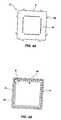
- FIG. 4Ais a top view of an image sensor package interposer according to a second embodiment of the present invention.
- FIG. 4Bis a bottom view of a package structure according to the second embodiment of the present invention.
- FIG. 4Cis a bottom perspective view of the package structure depicted in FIG. 4B .
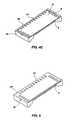
- FIG. 5is a bottom perspective view of a package structure according to a third embodiment of the present invention.
- FIG. 6shows a molding process for forming the package structure depicted in FIG. 5 .
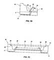
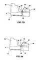
- FIG. 7Ais a cross-sectional side view of a package structure according to a fourth embodiment of the present invention.
- FIG. 7Bis an enlarged sectional view of the package structure depicted in FIG. 7A .
- FIG. 7Cis a cross-sectional side view of an image sensor package according to the fourth embodiment of the present invention.
- FIG. 7Dis an enlarged sectional view of the packaged structure depicted in FIG. 7A including an optional sealant.
- FIG. 8Ashows an enlarged sectional view of a package structure according to a fifth embodiment of the present invention.
- FIG. 8Bshows an enlarged sectional view of an alternative package structure according to the fifth embodiment of the present invention.
- FIG. 9Ais a cross-sectional side view of a flip-chip-configured image sensor package according to the fifth embodiment of the present invention.
- FIG. 9Bis an enlarged sectional view of the image sensor package depicted in FIG. 9A .
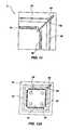
- FIG. 10is a top view of a package structure according to a sixth embodiment of the present invention.
- FIG. 11is an enlarged sectional view showing a channel formed in the package structure depicted in FIG. 10 .
- FIGS. 12A-12D and 13show a process for assembling and sealing an image sensor package according to the sixth embodiment of the present invention.
- the present inventionincludes package structures and methods of package assembly for image sensors such as solid state CCD or CMOS chips for receiving an image of reflected light or other electromagnetic radiation from one or more objects.
- the packages and methods of the present inventionwould also work well for enclosing other types of light or other radiation-sensitive electronic components such as, for example, erasable programmable read-only memory chips (EPROMs).
- EPROMserasable programmable read-only memory chips
- FIG. 1shows an interposer 2 that is utilized as a platform for the subsequent formation of image sensor package embodiments of the present invention.
- Interposer 2includes a chip surface 4 , an opposing attachment surface 6 , and peripheral edge surfaces 8 .
- Contact pads 10are formed on chip surface 4 for wire bond or flip-chip connection to an image sensor chip as described in further detail below.
- Internal conductive elements 12electrically connect contact pads 10 to attachment pads 14 on attachment surface 6 for connecting a completed image sensor package to a larger assembly such as a printed circuit board.
- Interposer 2may be formed of materials such as FR-4 and BT laminates or even plastic, which are less expensive and easier to manufacture than the ceramic substrates typically used for image sensor packages.
- interposer 2any conventional substrate materials, including ceramic, may be used to form interposer 2 if necessary or desirable based on other considerations besides cost. While interposer 2 is illustrated as being configured for assembly of a single image sensor package, it may also be formed as part of a larger substrate comprising multiple interposers. In this manner, several image sensor packages can be formed simultaneously on a single substrate, which is then singulated to provide individual image sensor packages.
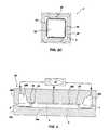
- FIGS. 2A-2Ca first embodiment of an image sensor package according to the present invention is illustrated.
- a housing structure 16is formed on interposer 2 that covers substantially all of chip surface 4 .
- Housing structure 16has raised sidewalls 18 around the perimeter of interposer 2 , thereby forming a chip cavity 20 for receiving an image sensor chip.
- Sidewalls 18include a ledge 22 that surrounds chip cavity 20 for receiving and supporting a transparent cover 46 ( FIG. 7C ).
- Housing structure 16also extends across the bottom surface 24 of chip cavity 20 and includes apertures 26 for exposing contact pads 10 of interposer 2 .
- FIG. 2Bshows a bottom view of interposer 2 with attachment pads 14 positioned around the perimeter of attachment surface 6 .
- attachment pads 14may have a matrix of attachment pads formed in an array pattern on attachment surface 6 .
- attachment pads 14might also have a circular shape to receive ball or spherically shaped external conductive elements.
- FIGS. 2A and 2Bshow that in the current embodiment, housing structure 16 does not cover attachment surface 6 or edge surfaces 8 of interposer 2 , but is instead limited to covering chip surface 4 in the manner shown by FIG. 2C .
- the area of interposer 2 at the bottom of chip cavity 20is entirely covered by housing structure 16 except for locations where apertures 26 are formed to expose contact pads 10 .
- FIG. 2Cillustrates that contact pads 10 are positioned in rows with a single aperture 26 exposing an entire row of contact pads. It is also possible that an aperture 26 may be provided for each contact pad, with material from housing structure 16 covering areas between adjacent contact pads.
- Housing structure 16may be formed on interposer 2 using conventional molding processes such as transfer molding, pot molding, or injection molding.
- FIG. 3shows an example of how housing structure 16 may be formed by a molding process.
- a molding tool 28is provided having a lower platen 28 a and an upper platen 28 b .
- Lower platen 28 aincludes a mold cavity 30 a which holds interposer 2 in sealing relationship against attachment surface 6 and edge surfaces 8 .
- Upper platen 28 bincludes a mold cavity 30 b that is positioned over chip surface 4 .
- mold cavity 30 bincludes protrusions 32 that seal against contact pads 10 to form apertures 26 in housing structure 16 .
- Mold cavity 30 bis then filled with a mold compound 34 in a liquid or otherwise molten state. Mold compound 34 is cured to an at least semisolid state, and interposer 2 is removed from molding tool 28 , leaving the housing structure 16 illustrated in FIGS. 2A-2C .
- mold cavities 30 a and 30 bmay be configured with a size and shape to form a housing structure onto the chip surface of each interposer, with subsequent singulation of the larger substrate providing individual image sensor packages. It is also possible that housing structure 16 could be premolded and then attached to interposer 2 with a layer of suitable adhesive material applied to one or both of chip surface 4 and housing structure 16 .
- Mold compound 34may be a thermoplastic polymer or other suitable encapsulant material as known in the art. Further, a filler material such as fine silicon particles may be incorporated within the mold compound 34 to reduce cost, also as known in the art. Other suitable known materials for mold compounds include, without limitation, thermoset polymers and epoxy compounds. Any other molding compounds may be employed to form housing structure 16 , however, it is desirable to use a material that exhibits low moisture absorption and a CTE (coefficient of thermal expansion) having a minimal difference from that of interposer 2 and transparent cover 46 ( FIG. 7C ).
- CTEcoefficient of thermal expansion
- FIGS. 4A-4Cshow a second embodiment of an image sensor package according to the present invention.
- interposer 2includes tie bars 36 that protrude from edge surfaces 8 .
- Tie bars 36provide spacing to enable mold compound 34 to cover edge surfaces 8 of interposer 2 during package formation.
- tie bars 36would abut against the sides of mold cavity 30 a in lower platen 28 a to center interposer 2 within mold cavity 30 a .
- mold compound 34enters the areas between the sides of mold cavity 30 a and edge surfaces 8 of interposer 2 .
- interposer 2is removed from molding tool 28 , leaving a housing structure 16 ′ that covers and seals chip surface 4 and all of edge surfaces 8 except for the outer ends of tie bars 36 , as illustrated by FIGS. 4B and 4C .
- the second image sensor package embodimentis well suited for situations where interposer 2 comprises a laminate-type substrate with minute gaps between laminate layers that are exposed to the outside environment and may absorb moisture.
- the second embodimentis also applicable where interposer 2 is formed as part of a larger substrate containing multiple interposers. For example, slots or openings may be formed in the larger substrate at locations between the interposer 2 , leaving portions of substrate material between the interposers to act as tie bars 36 . In this manner, tie bars 36 hold the interposers together while enabling mold compound 34 to cover edge surfaces 8 of all the interposers.
- the cured molding compound 34 and tie bars 36 between adjacent interposers 2are cut or otherwise separated to provide individual image sensor packages.
- FIG. 5shows a third embodiment of an image sensor package according to the present invention that addresses this problem.
- a housing structure 16 ′′is formed on interposer 2 that covers substantially all of chip surface 4 and edge surfaces 8 , and also covers substantially the entire attachment surface 6 of the interposer 2 , leaving only the external attachment pads 14 exposed.
- FIG. 6shows an exemplary molding process for forming housing structure 16 ′′.
- molding tool 28is modified such that lower platen 28 a has a mold cavity 30 a ′ that does not seal against attachment surface 6 of interposer 2 .
- mold cavity 30 a ′includes protrusions 38 that raise interposer 2 up from the bottom of mold cavity 30 a ′ and seal against attachment pads 14 .
- interposer 2has tie bars 36 that abut against the sides of mold cavity 30 a ′ in lower platen 28 a to center interposer 2 within mold cavity 30 a ′.
- mold compound 34passes through the areas between the sides of mold cavity 30 a ′ and edge surfaces 8 of interposer 2 , thereby filling the bottom of mold cavity 30 a ′ and covering attachment surface 6 .
- interposer 2is removed from molding tool 28 , leaving housing structure 16 ′′ that covers and seals substantially all of chip surface 4 , edge surfaces 8 , and attachment surface 6 as illustrated by FIG. 5 .
- tie bars 36may be formed in the same manner as described in the second embodiment and used to hold the interposers together during the molding process.
- the spaces between each interposerprovide additional areas for mold compound 34 to pass into mold cavity 30 a ′ in order to cover attachment surface 6 .
- mold cavities 30 a ′ and 30 bare configured with a size and shape for molding large substrates containing multiple interposers, it may also be desirable to supply mold compound 34 directly to mold cavity 30 a ′ while filling mold cavity 30 b to ensure uniform coverage.
- housing structures 16 - 16 ′′are also contemplated by the present invention.
- One such alternativeincludes disposing a flowable material over the surfaces of interposer 2 in one or more sequentially cured layers to build housing structures 16 - 16 ′′.
- a high-viscosity liquid or gelsuch as an epoxy may be dispensed from a nozzle onto chip surface 4 .
- the high-viscosity liquid or gelis then cured to form a first hardened layer.
- An additional layer of high-viscosity liquid or gelis dispensed over the first hardened layer and cured to form second hardened layer. Subsequent layers of liquid or gel may be added, as necessary, until the desired shape for housing structure 16 is formed.
- housing structure 16 ′the liquid or gel may simply be deposited in layers along edge surfaces 8 while covering chip surface 4 . With this method, tie bars 36 are not required to provide mold spacing, and edge surfaces 8 may be completely sealed from the outside environment. Once chip surface 4 and edge surfaces 8 are covered, the same process may be used to cover attachment surface 6 , thereby forming housing structure 16 ′′.
- STLstereolithographic
- a stereolithographic (STL) deposition processto faun housing structures 16 - 16 ′′.
- STLinvolves the formation of solid structures by selectively curing portions of volumes of a photocurable liquid polymer or resin material contained within a tank or reservoir.
- curingmay be accomplished by exposure to irradiation with selected wavelengths of light or other electromagnetic radiation, for instance, when curing a material susceptible to initiation of cross-linking by exposure to ultraviolet (UV) radiation, such as through use of a UV laser beam.
- UV radiationultraviolet
- FIGS. 7A-9Bshow alternative embodiments of how an image sensor chip may be mounted within chip cavity 20 and electrically connected to contact pads 10 of interposer 2 . While the following embodiments are described in terms of housing structure 16 , it should be understood that they also apply to mounting of image sensor chips within housing structures 16 ′ and 16 ′′.
- FIGS. 7A-7Dshow a fourth embodiment of an image sensor package according to the present invention wherein an image sensor chip 40 is wire bonded directly to contact pads 10 exposed through apertures 26 of housing structure 16 .
- image sensor chip 40is attached to the bottom surface 24 of chip cavity 20 between opposing rows of contact pads 10 . Attachment of image sensor chip 40 may be accomplished with an adhesive material (not shown) applied to one or both of bottom surface 24 and image sensor chip 40 .
- FIG. 7Bshows that once image sensor chip 40 is in place, bond wires 42 are attached between contact pads 10 of interposer 2 and bond pads 44 of image sensor chip 40 to provide electrical connection.
- a transparent cover 46may be set onto ledge 22 of housing structure 16 and sealed in place to provide a completed image sensor package 48 , as illustrated by FIG. 7C .
- Transparent cover 46may be formed of an at least partially optically transparent material such as borosilicate glass (BSG). Of course, other types of glass, quartz or even plastic which enable the passage of a desired range of wavelengths of light or other forms of electromagnetic radiation may also be used.
- transparent cover 46may be formed to provide an optical function, for example, shaping its surface at locations above chip cavity 20 to provide focusing capabilities.
- a bead of epoxy, silicone gel or other liquid or gel adhesive sealant 50may be applied along the edge of transparent cover 46 as shown in FIG. 7C .
- a two-component adhesive resinmay be employed, with one component applied to ledge 22 and the other to transparent cover 46 so that a cure will not commence until the two components are in contact.
- Other known sealing mechanismsmay be used as well, as long as they provide a suitable hermetic bond. It is desirable, so that the optical capabilities of image sensor chip 40 are not compromised, that any adhesive used be of a type which does not outgas volatiles or other compounds when curing.
- a snap-cure epoxymay be suitable, as may an epoxy cured to a B-stage, or tacky state, prior to application of transparent cover 46 .
- Another possibilityis to form housing structure 16 with a runner that provides a space for venting gases from chip cavity 20 while adhesive sealant 50 cures, as described in further detail below.
- FIG. 7Dshows that liquid sealant 52 is deposited within apertures 26 to accomplish this complete sealing.
- Liquid sealant 52may be any material that exhibits low moisture permeability and bonds well to the surrounding housing structure 16 .
- Conventional UV or thermally cured epoxy adhesives, for example,may be suitable for this application.
- FIG. 8Ashows a fifth embodiment of an image sensor package according to the present invention where apertures 26 are first filled with a conductive material 54 up to a level that is substantially even with the bottom surface 24 of the chip cavity 20 . In this manner, contact pads 10 are built up to further seal interposer 2 from chip cavity 20 . Furthermore, bond wires 42 may then be attached to conductive material 54 at a level that is substantially even with bottom surface 24 , eliminating the difficulties with having to attach a bond wire 42 within the relatively small space provided by apertures 26 . Filling of apertures 26 may be carried out with conventional metal deposition processes such as chemical-vapor deposition (CVD), depositing a conductive or conductor-filled epoxy, or simply by depositing and reflowing solder paste within apertures 26 .
- FIG. 8Bshows that in the case where conductive material 54 is a solder paste, it may not completely fill apertures 26 because flux material is driven off during reflow. In this situation, liquid sealant 52 may be deposited over conductive material 54 to completely fill apertures 26
- FIGS. 9A and 9Bshow an alternative to the fifth embodiment of the present invention wherein image sensor chip 40 is attached directly to the built-up conductive material 54 over contact pads 10 in a flip-chip manner, such that bond wires 42 are not required.
- image sensor chip 40includes through-hole vias 56 connected to bottom-side bond pads 58 on image sensor chip 40 .
- the formation of through-hole vias 56may be accomplished by laser cutting or etching holes in image sensor chip 40 and filling the holes with conductive material. Such via formation processes are known in the art and need not be described further with respect to carrying out the present invention.
- contact pads 10 of interposer 2may be located underneath, rather than peripheral to, image sensor chip 40 .
- contact pads 10may be positioned in an array-type pad layout across the entire bottom surface 24 of chip cavity 20 , enabling image sensor chips having higher I/O requirements to be mounted within the same area.
- Image sensor chip 40is secured within chip cavity 20 by attaching bottom-side bond pads 58 to conductive material 54 with a conductive bond.
- a conductive adhesive materialmay be used for this purpose, such as conductive or conductor-filled epoxies, or with a film of anisotropically conductive adhesive material that is applied to cover all of the bonding areas.
- bottom-side bond pads 58may simply be set in place and bonded to by curing the epoxy or reflowing the solder paste.
- FIG. 9Bshows that the flip-chip mounting embodiment may optionally include deposition of an underfill 60 by capillary flow of a liquid sealing material to fill gaps between bottom surface 24 of chip cavity 20 and image sensor chip 40 .
- underfill 60reinforces the conductive bonds to image sensor chip 40 and seals out contamination that may cause shorting between bond locations.
- any of housing structures 16 - 16 ′′may be provided with one or more runners that enable sealing the bottom surface 24 of chip cavity 20 simultaneously with the sealing of transparent cover 46 .
- FIGS. 10-13show an example of this embodiment of the invention. While FIGS. 10-13 are described in terms of housing structure 16 , it should be understood that the present embodiment is also applicable to housing structures 16 ′ and 16 ′′.
- FIG. 10shows that housing structure 16 is formed with a ledge 22 surrounding chip cavity 20 for supporting the edges of transparent cover 46 (not shown).
- Ledge 22acts as a runner for adhesive sealant 50 to fill the space between the edges of transparent cover 46 and housing structure 16 .
- adhesive sealant 50comprises a liquid epoxy.
- other curable liquid sealants suitable for deposition by capillary flowmay also be used, as long as they are capable of forming a hermetic seal.
- At least one additional runneris formed by a channel 62 that extends from ledge 22 down to bottom surface 24 of chip cavity 20 .
- FIG. 11is an enlarged view of area A in FIG. 10 that more clearly shows channel 62 formed to extend down a corner of chip cavity 20 .
- FIG. 11also shows that a sealing well 64 is formed in housing structure 16 to provide an expanded opening adjacent to the junction of channel 62 and ledge 22 .
- FIGS. 12A-13an exemplary assembly process is illustrated to show how the present embodiment enables simultaneous sealing of bottom surface 24 and transparent cover 46 .
- an epoxy 66 or other suitable adhesive materialis deposited on bottom surface 24 .
- image sensor chip 40is mounted within chip cavity 20 by attachment to epoxy 66 .
- bond pads 44 on the top of image sensor chip 40are electrically connected to contact pads 10 with bond wires 42 , as shown in FIG. 12C .
- transparent cover 46is placed on ledge 22 of housing structure 16 .
- sealing well 64provides an opening at the corner of transparent cover 46 through which adhesive sealant 50 may be injected into the runner areas formed by ledge 22 and channel 62 .
- FIG. 13is a sectional view of image sensor package 48 taken along line 13 - 13 in FIG. 12D .
- FIG. 13shows that after transparent cover 46 is placed on ledge 22 , adhesive sealant 50 is dispensed from a nozzle 68 into sealing well 64 , and by capillary action flows around the runner area of ledge 22 to fill the space between housing structure 16 and transparent cover 46 .
- capillary flow of adhesive sealant 50 down channel 62covers and further seals bottom surface 24 of chip cavity 20 .
- adhesive sealant 50may be used to fill apertures 26 , eliminating the need to perform a separate filling operation with liquid sealant 52 as described above with respect to the fourth and fifth embodiments of the present invention.
- sealing well 64may be filled to completely seal chip cavity 20 from the outside environment.
- An additional benefit of this processis that while sealing well 64 remains unfilled, volatiles or other compounds produced by the curing of adhesive sealant 50 within chip cavity 20 may be outgassed through the remaining opening.
- FIGS. 12A-13show sealing for an image sensor package with a wire-bonded configuration
- this sealing structure and methodmay also be used for the flip-chip mounted image sensor chip 40 illustrated in FIGS. 9A and 9B .
- the capillary flow of adhesive sealant 50fills the spaces between image sensor chip 40 and bottom surface 24 of chip cavity 20 , eliminating the need to perform a separate operation for forming underfill 60 .
- FIGS. 12A-13depict a single channel 62 formed along a corner of chip cavity 20 , other configurations are possible. Channel 62 and sealing well 64 may be formed at other locations along the perimeter of ledge 22 , and multiple channels could be formed to allow flow of adhesive sealant 50 down to bottom surface 24 .
- any of the above-described housing structures 16 - 16 ′′may also be formed without covering the area of interposer 2 underlying chip cavity 20 . In this manner, package formation is simplified because there is no requirement to wire bond within apertures 26 or to carry out additional operations to fill them with conductive material 54 .
- adhesive sealant 50covers any areas not sealed by the housing structures.
Landscapes
- Engineering & Computer Science (AREA)
- Computer Hardware Design (AREA)
- Microelectronics & Electronic Packaging (AREA)
- Power Engineering (AREA)
- Physics & Mathematics (AREA)
- Condensed Matter Physics & Semiconductors (AREA)
- General Physics & Mathematics (AREA)
- Manufacturing & Machinery (AREA)
- Solid State Image Pick-Up Elements (AREA)
Abstract
Description
- This application is a continuation of application Ser. No. 11/366,793, pending, filed Mar. 2, 2006, which is a continuation of application Ser. No. 11/180,493, filed Jul. 13, 2005, now U.S. Pat. No. 7,026,548, issued Apr. 11, 2006, which is a continuation of application Ser. No. 10/663,959, filed Sep. 16, 2003, now U.S. Pat. No. 6,953,891, issued Oct. 11, 2005. The disclosure of each of the foregoing documents is hereby incorporated by reference in its entirety herein.
- 1. Field of the Invention
- The present invention relates generally to packaging of electronic devices for protection from external environmental conditions. More particularly, the present invention relates to moisture-resistant packages with transparent covers for enclosing solid-state image sensors or similar electronic devices that are sensitive to light or other forms of radiation.
- 2. State of the Art
- Solid-state image sensors, for example, charge coupled devices (CCDs) or complementary metal-oxide semiconductor (CMOS) chips, are increasingly in demand for use with electronic products such as digital cameras. Conventionally, these sensors have been packaged for use by mounting them to a substrate and enclosing them within a housing assembly. The housing assembly incorporates a transparent lid to allow light or other forms of radiation to be received by the sensor. The lid may be a flat window or shaped as a lens to provide optical properties. The substrate and housing are often formed from a ceramic material, and the lid is glass or a similar transparent substance attached to the housing by an adhesive. Due to the materials and structure involved, this packaging technique may be expensive and difficult to manufacture.
- In order to overcome these problems, various methods have been developed in attempts to simplify the construction of image sensor packages and reduce material costs. One such approach has been to fabricate packages by using molded housing assemblies that are attached to, or formed on, substrates of low-cost materials like BT/epoxy laminates or plastic. Examples include U.S. Pat. No. 5,811,799 to Wu and U.S. Pat. No. 6,266,197 to Glenn et al. U.S. Pat. No. 6,906,403, issued Jun. 14, 2005, and pending U.S. patent application Ser. No. 10/228,411, filed Aug. 26, 2002, both assigned to the assignee of the present invention, also disclose image sensor packages of this type.
- While these and other designs have been beneficial with respect to reducing the cost of manufacturing, they raise other concerns. Image sensor packages constructed from materials such as those described above may not provide the same hermetic sealing capabilities as prior art ceramic packaging. Glass laminate-type substrates, for instance, are not completely impermeable and may absorb moisture, especially at edge locations where minute gaps between laminate layers are exposed to the outside environment. This moisture may ultimately find its way into the interior of the package, resulting in damage to the image sensor circuitry. Moisture absorption may also cause deformations in the substrate that will negatively affect the focal properties of the package. Another problem arises from the use of a molded housing, which does not have the high dimensional tolerances of ceramics and may cause difficulties with sealing to the substrate and transparent lid.
- The increasing number of portable electronic products intended for use in extreme environments makes reliable sealing of image sensors an even more important aspect of any packaging structure. What is needed is an image sensor package that is simple and inexpensive to manufacture, and that also provides reliable hermetic sealing capabilities to prevent moisture damage and other harmful environmental effects.
- In accordance with the present invention, improved packages for electronic devices and methods for their assembly are disclosed. Embodiments of the present invention are directed to image sensor chips. However, packaging of any other light or radiation-sensitive electronic components is also contemplated as being within the scope of the present invention. In a basic form, an image sensor package according to the present invention comprises a housing structure formed on an interposer substrate by molding or other deposition process. The chips are mounted in a chip cavity formed by the housing structure and electrically connected to interposer contact pads that are exposed through the housing structure within the chip cavity. The chip cavity is then sealed by a transparent cover which acts as a window or lens. Once assembled, the image sensor package may be incorporated into electronic devices by connection to external attachment pads on the interposer. The packages are inexpensive and simple to construct while exhibiting durability and improved sealing properties.
- In one embodiment according to the present invention, an image sensor package is assembled by forming a housing structure that covers substantially the entire chip surface of the interposer, leaving only a small area of the chip surface immediately surrounding the interposer contact pads exposed through apertures within the housing structure for connection to the image sensor chip. As used herein, the term “chip surface” refers to the side of the interposer on which image sensor chips are mounted within the chip cavity.
- In another embodiment according to the present invention, the interposer may also include peripheral structures in the form of tie bars or other protrusions that extend from the edge surfaces of the interposer. The tie bars provide spacing to enable mold material to cover the edge surfaces of the interposer when forming the housing structure. The tie bars may also be used to connect a strip or array of interposers, thereby enabling multiple housing structures to be formed simultaneously on a single substrate and subsequently separated into individual image sensor packages.
- In another embodiment according to the present invention, the housing structure also covers substantially the entire attachment surface of the interposer, leaving only the area of the attachment surface immediately surrounding the external attachment pads exposed. As used herein, the term “attachment surface” refers to the side of the interposer which is opposite the chip surface of the interposer.
- In another embodiment according to the present invention, bond pads of the image sensor chip are attached directly to the interposer contact pads exposed through the apertures in the housing structure with wire bonds. The apertures may optionally be filled with a liquid sealant to further seal the interposer from the chip cavity.
- In another embodiment according to the present invention, the apertures that expose the interposer contact pads are first filled with a conductive material up to a level that is substantially even with the bottom of the chip cavity. In this manner, the contact pads are built up to further seal the interposer from the chip cavity. Bond wires may then be attached to the built-up pads at a level that is substantially even with the bottom of the chip cavity, rather than in the relatively small space provided by the apertures in the housing structure exposing the contact pads. A liquid sealant may also be applied to further seal the connection between the built-up pads and the bond wires.
- In an alternative to the above embodiment, the bond pads of the image sensor chip are attached directly to the built-up pads in a flip-chip manner, such that bond wires are not required. A liquid sealant may be applied under the image sensor chip in a capillary process to further seal the connection between the image sensor bond pads and the built-up pads.
- In another embodiment according to the present invention, the housing structure is provided with runners that enable sealing the bottom of the chip cavity simultaneously with sealing the transparent cover to the housing structure. Under this embodiment, a ledge surrounding the chip cavity for supporting edges of the transparent cover acts as a runner for a sealant that fills the space between the edges of the transparent cover and the molded housing structure. At least one additional runner is formed by a channel that extends from the ledge down to the bottom surface of the chip cavity. After the transparent cover is placed on the ledge of the housing structure, a liquid sealant is injected into a sealing well formed in the housing structure adjacent to the runner areas. Capillary flow of the liquid sealant along the ledge fills the space between the edges of the transparent cover and the housing structure. At the same time, capillary flow of the liquid sealant along the additional runner or runners covers the bottom surface of the chip cavity to seal any exposed areas of the interposer.
- Other and further features and advantages will be apparent from the following descriptions of the various embodiments of the present invention when read in conjunction with the accompanying drawings. It should be understood that the following descriptions are provided for illustrative and exemplary purposes only, and that numerous combinations of the elements of the various embodiments of the present invention are possible.
- In the drawings, which illustrate what is currently considered to be the best mode for carrying out the invention:
FIG. 1 is a cross-sectional side view of an image sensor package interposer according to the present invention.FIG. 2A is a cross-sectional side view of a first embodiment of a package structure according to the present invention.FIG. 2B is a bottom view of the package structure depicted inFIG. 2A .FIG. 2C is a top view of the package structure depicted inFIG. 2A .FIG. 3 shows a molding process for forming the package structure depicted inFIG. 2A .FIG. 4A is a top view of an image sensor package interposer according to a second embodiment of the present invention.FIG. 4B is a bottom view of a package structure according to the second embodiment of the present invention.FIG. 4C is a bottom perspective view of the package structure depicted inFIG. 4B .FIG. 5 is a bottom perspective view of a package structure according to a third embodiment of the present invention.FIG. 6 shows a molding process for forming the package structure depicted inFIG. 5 .FIG. 7A is a cross-sectional side view of a package structure according to a fourth embodiment of the present invention.FIG. 7B is an enlarged sectional view of the package structure depicted inFIG. 7A .FIG. 7C is a cross-sectional side view of an image sensor package according to the fourth embodiment of the present invention.FIG. 7D is an enlarged sectional view of the packaged structure depicted inFIG. 7A including an optional sealant.FIG. 8A shows an enlarged sectional view of a package structure according to a fifth embodiment of the present invention.FIG. 8B shows an enlarged sectional view of an alternative package structure according to the fifth embodiment of the present invention.FIG. 9A is a cross-sectional side view of a flip-chip-configured image sensor package according to the fifth embodiment of the present invention.FIG. 9B is an enlarged sectional view of the image sensor package depicted inFIG. 9A .FIG. 10 is a top view of a package structure according to a sixth embodiment of the present invention.FIG. 11 is an enlarged sectional view showing a channel formed in the package structure depicted inFIG. 10 .FIGS. 12A-12D and13 show a process for assembling and sealing an image sensor package according to the sixth embodiment of the present invention.- As described below, the present invention includes package structures and methods of package assembly for image sensors such as solid state CCD or CMOS chips for receiving an image of reflected light or other electromagnetic radiation from one or more objects. However, the packages and methods of the present invention would also work well for enclosing other types of light or other radiation-sensitive electronic components such as, for example, erasable programmable read-only memory chips (EPROMs).
- Referring initially to the accompanying drawings, various aspects of the present invention are illustrated to show exemplary image sensor package structures and methods for their assembly. To simplify the description of the present invention, common elements of the various embodiments illustrated by the drawings are designated with like reference numerals. The figures presented by the drawings are not meant to be illustrative of actual views of any particular portion of a particular image sensor package structure, but are merely idealized schematic representations which are employed to assist in clearly and fully describing the invention.
FIG. 1 shows aninterposer 2 that is utilized as a platform for the subsequent formation of image sensor package embodiments of the present invention.Interposer 2 includes a chip surface4, an opposingattachment surface 6, and peripheral edge surfaces8. Contactpads 10 are formed on chip surface4 for wire bond or flip-chip connection to an image sensor chip as described in further detail below. Internalconductive elements 12 electrically connectcontact pads 10 toattachment pads 14 onattachment surface 6 for connecting a completed image sensor package to a larger assembly such as a printed circuit board.Interposer 2 may be formed of materials such as FR-4 and BT laminates or even plastic, which are less expensive and easier to manufacture than the ceramic substrates typically used for image sensor packages. Of course, any conventional substrate materials, including ceramic, may be used to forminterposer 2 if necessary or desirable based on other considerations besides cost. Whileinterposer 2 is illustrated as being configured for assembly of a single image sensor package, it may also be formed as part of a larger substrate comprising multiple interposers. In this manner, several image sensor packages can be formed simultaneously on a single substrate, which is then singulated to provide individual image sensor packages.- Turning to
FIGS. 2A-2C , a first embodiment of an image sensor package according to the present invention is illustrated. As seen inFIG. 2A , ahousing structure 16 is formed oninterposer 2 that covers substantially all of chip surface4.Housing structure 16 has raisedsidewalls 18 around the perimeter ofinterposer 2, thereby forming achip cavity 20 for receiving an image sensor chip.Sidewalls 18 include aledge 22 that surroundschip cavity 20 for receiving and supporting a transparent cover46 (FIG. 7C ).Housing structure 16 also extends across thebottom surface 24 ofchip cavity 20 and includesapertures 26 for exposingcontact pads 10 ofinterposer 2. FIG. 2B shows a bottom view ofinterposer 2 withattachment pads 14 positioned around the perimeter ofattachment surface 6. It should be understood that the location and shape ofattachment pads 14 illustrated inFIG. 2B are only exemplary, and that any other known pad layout is possible. Image sensor packages requiring a high number of I/O connections, for instance, may have a matrix of attachment pads formed in an array pattern onattachment surface 6. Rather than being rectangular,attachment pads 14 might also have a circular shape to receive ball or spherically shaped external conductive elements.FIGS. 2A and 2B show that in the current embodiment,housing structure 16 does not coverattachment surface 6 oredge surfaces 8 ofinterposer 2, but is instead limited to covering chip surface4 in the manner shown byFIG. 2C . As seen inFIG. 2C , the area ofinterposer 2 at the bottom ofchip cavity 20 is entirely covered byhousing structure 16 except for locations whereapertures 26 are formed to exposecontact pads 10.FIG. 2C illustrates thatcontact pads 10 are positioned in rows with asingle aperture 26 exposing an entire row of contact pads. It is also possible that anaperture 26 may be provided for each contact pad, with material fromhousing structure 16 covering areas between adjacent contact pads.Housing structure 16 may be formed oninterposer 2 using conventional molding processes such as transfer molding, pot molding, or injection molding.FIG. 3 shows an example of howhousing structure 16 may be formed by a molding process. Amolding tool 28 is provided having alower platen 28aand anupper platen 28b.Lower platen 28aincludes amold cavity 30awhich holdsinterposer 2 in sealing relationship againstattachment surface 6 and edge surfaces8.Upper platen 28bincludes amold cavity 30bthat is positioned over chip surface4. As seen inFIG. 3 ,mold cavity 30bincludesprotrusions 32 that seal againstcontact pads 10 to formapertures 26 inhousing structure 16.Mold cavity 30bis then filled with amold compound 34 in a liquid or otherwise molten state.Mold compound 34 is cured to an at least semisolid state, andinterposer 2 is removed frommolding tool 28, leaving thehousing structure 16 illustrated inFIGS. 2A-2C .- In the situation where
interposer 2 is formed as part of a larger substrate containing multiple interposers,mold cavities housing structure 16 could be premolded and then attached tointerposer 2 with a layer of suitable adhesive material applied to one or both of chip surface4 andhousing structure 16. Mold compound 34 may be a thermoplastic polymer or other suitable encapsulant material as known in the art. Further, a filler material such as fine silicon particles may be incorporated within themold compound 34 to reduce cost, also as known in the art. Other suitable known materials for mold compounds include, without limitation, thermoset polymers and epoxy compounds. Any other molding compounds may be employed to formhousing structure 16, however, it is desirable to use a material that exhibits low moisture absorption and a CTE (coefficient of thermal expansion) having a minimal difference from that ofinterposer 2 and transparent cover46 (FIG. 7C ).FIGS. 4A-4C show a second embodiment of an image sensor package according to the present invention. As seen inFIG. 4A , with the second embodiment,interposer 2 includes tie bars36 that protrude from edge surfaces8. Tie bars36 provide spacing to enablemold compound 34 to cover edge surfaces8 ofinterposer 2 during package formation. With the molding process illustrated inFIG. 3 , for instance, tie bars36 would abut against the sides ofmold cavity 30ainlower platen 28atocenter interposer 2 withinmold cavity 30a. Whenmold cavity 30bis filled,mold compound 34 enters the areas between the sides ofmold cavity 30aandedge surfaces 8 ofinterposer 2. After curingmold compound 34,interposer 2 is removed frommolding tool 28, leaving ahousing structure 16′ that covers and seals chip surface4 and all ofedge surfaces 8 except for the outer ends of tie bars36, as illustrated byFIGS. 4B and 4C .- The second image sensor package embodiment is well suited for situations where
interposer 2 comprises a laminate-type substrate with minute gaps between laminate layers that are exposed to the outside environment and may absorb moisture. The second embodiment is also applicable whereinterposer 2 is formed as part of a larger substrate containing multiple interposers. For example, slots or openings may be formed in the larger substrate at locations between theinterposer 2, leaving portions of substrate material between the interposers to act as tie bars36. In this manner, tie bars36 hold the interposers together while enablingmold compound 34 to cover edge surfaces8 of all the interposers. Once package formation is complete, the curedmolding compound 34 and tie bars36 betweenadjacent interposers 2 are cut or otherwise separated to provide individual image sensor packages. - In some instances, it may be desirable to seal all of the surfaces of
interposer 2 from the outside environment. Such sealing not only helps prevent moisture from enteringchip cavity 20, but also further limits any moisture that may be absorbed byinterposer 2. Moisture absorption byinterposer 2 is a concern as it may cause warping or other deformations in shape that will negatively affect the focal properties of a completed image sensor package.FIG. 5 shows a third embodiment of an image sensor package according to the present invention that addresses this problem. As seen inFIG. 5 , with the third embodiment, ahousing structure 16″ is formed oninterposer 2 that covers substantially all of chip surface4 andedge surfaces 8, and also covers substantially theentire attachment surface 6 of theinterposer 2, leaving only theexternal attachment pads 14 exposed. FIG. 6 shows an exemplary molding process for forminghousing structure 16″. According to the third embodiment,molding tool 28 is modified such thatlower platen 28ahas amold cavity 30a′ that does not seal againstattachment surface 6 ofinterposer 2. Instead,mold cavity 30a′ includesprotrusions 38 that raiseinterposer 2 up from the bottom ofmold cavity 30a′ and seal againstattachment pads 14. As in the second embodiment,interposer 2 has tie bars36 that abut against the sides ofmold cavity 30a′ inlower platen 28atocenter interposer 2 withinmold cavity 30a′. Whenmold cavity 30bis filled,mold compound 34 passes through the areas between the sides ofmold cavity 30a′ andedge surfaces 8 ofinterposer 2, thereby filling the bottom ofmold cavity 30a′ and coveringattachment surface 6. After curingmold compound 34,interposer 2 is removed frommolding tool 28, leavinghousing structure 16″ that covers and seals substantially all of chip surface4, edge surfaces8, andattachment surface 6 as illustrated byFIG. 5 .- Where
interposer 2 is formed as part of a larger substrate containing multiple interposers, tie bars36 may be formed in the same manner as described in the second embodiment and used to hold the interposers together during the molding process. The spaces between each interposer provide additional areas formold compound 34 to pass intomold cavity 30a′ in order to coverattachment surface 6. When mold cavities30a′ and30bare configured with a size and shape for molding large substrates containing multiple interposers, it may also be desirable to supplymold compound 34 directly tomold cavity 30a′ while fillingmold cavity 30bto ensure uniform coverage. - It will be understood by one of ordinary skill in the art that the molding processes described with respect to the above embodiments are only exemplary, and that other methods may be used to apply mold material to the various surfaces of
interposer 2. - Other alternatives to forming housing structures16-16″ are also contemplated by the present invention. One such alternative includes disposing a flowable material over the surfaces of
interposer 2 in one or more sequentially cured layers to build housing structures16-16″. To formhousing structure 16, for example, a high-viscosity liquid or gel such as an epoxy may be dispensed from a nozzle onto chip surface4. The high-viscosity liquid or gel is then cured to form a first hardened layer. An additional layer of high-viscosity liquid or gel is dispensed over the first hardened layer and cured to form second hardened layer. Subsequent layers of liquid or gel may be added, as necessary, until the desired shape forhousing structure 16 is formed. To formhousing structure 16′, the liquid or gel may simply be deposited in layers along edge surfaces8 while covering chip surface4. With this method, tie bars36 are not required to provide mold spacing, andedge surfaces 8 may be completely sealed from the outside environment. Once chip surface4 andedge surfaces 8 are covered, the same process may be used to coverattachment surface 6, thereby forminghousing structure 16″. - Another example of this layering approach exists in using a stereolithographic (STL) deposition process to faun housing structures16-16″. As defined in the art, STL involves the formation of solid structures by selectively curing portions of volumes of a photocurable liquid polymer or resin material contained within a tank or reservoir. Depending on the liquid material composition, curing may be accomplished by exposure to irradiation with selected wavelengths of light or other electromagnetic radiation, for instance, when curing a material susceptible to initiation of cross-linking by exposure to ultraviolet (UV) radiation, such as through use of a UV laser beam. By curing one or more successive layers of the liquid material, intricate solid structures of almost any shape may be formed.
- After a housing structure16-16″ has been formed on
interposer 2, an image sensor chip may be mounted withinchip cavity 20.FIGS. 7A-9B show alternative embodiments of how an image sensor chip may be mounted withinchip cavity 20 and electrically connected to contactpads 10 ofinterposer 2. While the following embodiments are described in terms ofhousing structure 16, it should be understood that they also apply to mounting of image sensor chips withinhousing structures 16′ and16″. FIGS. 7A-7D show a fourth embodiment of an image sensor package according to the present invention wherein animage sensor chip 40 is wire bonded directly to contactpads 10 exposed throughapertures 26 ofhousing structure 16. As seen inFIG. 7A ,image sensor chip 40 is attached to thebottom surface 24 ofchip cavity 20 between opposing rows ofcontact pads 10. Attachment ofimage sensor chip 40 may be accomplished with an adhesive material (not shown) applied to one or both ofbottom surface 24 andimage sensor chip 40.FIG. 7B shows that onceimage sensor chip 40 is in place,bond wires 42 are attached betweencontact pads 10 ofinterposer 2 andbond pads 44 ofimage sensor chip 40 to provide electrical connection.- At this point, a
transparent cover 46 may be set ontoledge 22 ofhousing structure 16 and sealed in place to provide a completedimage sensor package 48, as illustrated byFIG. 7C .Transparent cover 46 may be formed of an at least partially optically transparent material such as borosilicate glass (BSG). Of course, other types of glass, quartz or even plastic which enable the passage of a desired range of wavelengths of light or other forms of electromagnetic radiation may also be used. Furthermore,transparent cover 46 may be formed to provide an optical function, for example, shaping its surface at locations abovechip cavity 20 to provide focusing capabilities. - To secure
transparent cover 46 in place and hermetically sealimage sensor chip 40 withinchip cavity 20, a bead of epoxy, silicone gel or other liquid orgel adhesive sealant 50 may be applied along the edge oftransparent cover 46 as shown inFIG. 7C . If desired, a two-component adhesive resin may be employed, with one component applied toledge 22 and the other totransparent cover 46 so that a cure will not commence until the two components are in contact. Other known sealing mechanisms may be used as well, as long as they provide a suitable hermetic bond. It is desirable, so that the optical capabilities ofimage sensor chip 40 are not compromised, that any adhesive used be of a type which does not outgas volatiles or other compounds when curing. A snap-cure epoxy, as known in the art, may be suitable, as may an epoxy cured to a B-stage, or tacky state, prior to application oftransparent cover 46. Another possibility is to formhousing structure 16 with a runner that provides a space for venting gases fromchip cavity 20 whileadhesive sealant 50 cures, as described in further detail below. - With the fourth embodiment of the present invention, it may sometimes be desirable to completely seal the
bottom surface 24 ofchip cavity 20 by filling inapertures 26 prior to attachingtransparent cover 46.FIG. 7D shows thatliquid sealant 52 is deposited withinapertures 26 to accomplish this complete sealing.Liquid sealant 52 may be any material that exhibits low moisture permeability and bonds well to thesurrounding housing structure 16. Conventional UV or thermally cured epoxy adhesives, for example, may be suitable for this application. FIG. 8A shows a fifth embodiment of an image sensor package according to the present invention whereapertures 26 are first filled with aconductive material 54 up to a level that is substantially even with thebottom surface 24 of thechip cavity 20. In this manner,contact pads 10 are built up tofurther seal interposer 2 fromchip cavity 20. Furthermore,bond wires 42 may then be attached toconductive material 54 at a level that is substantially even withbottom surface 24, eliminating the difficulties with having to attach abond wire 42 within the relatively small space provided byapertures 26. Filling ofapertures 26 may be carried out with conventional metal deposition processes such as chemical-vapor deposition (CVD), depositing a conductive or conductor-filled epoxy, or simply by depositing and reflowing solder paste withinapertures 26.FIG. 8B shows that in the case whereconductive material 54 is a solder paste, it may not completely fillapertures 26 because flux material is driven off during reflow. In this situation,liquid sealant 52 may be deposited overconductive material 54 to completely fillapertures 26.FIGS. 9A and 9B show an alternative to the fifth embodiment of the present invention whereinimage sensor chip 40 is attached directly to the built-upconductive material 54 overcontact pads 10 in a flip-chip manner, such thatbond wires 42 are not required. As seen inFIG. 9A ,image sensor chip 40 includes through-hole vias 56 connected to bottom-side bond pads 58 onimage sensor chip 40. The formation of through-hole vias 56 may be accomplished by laser cutting or etching holes inimage sensor chip 40 and filling the holes with conductive material. Such via formation processes are known in the art and need not be described further with respect to carrying out the present invention. By using a flip-chip configuration, it is possible to mount a largerimage sensor chip 40 withinchip cavity 20 becausecontact pads 10 ofinterposer 2 may be located underneath, rather than peripheral to,image sensor chip 40. Furthermore,contact pads 10 may be positioned in an array-type pad layout across theentire bottom surface 24 ofchip cavity 20, enabling image sensor chips having higher I/O requirements to be mounted within the same area.Image sensor chip 40 is secured withinchip cavity 20 by attaching bottom-side bond pads 58 toconductive material 54 with a conductive bond. A conductive adhesive material may be used for this purpose, such as conductive or conductor-filled epoxies, or with a film of anisotropically conductive adhesive material that is applied to cover all of the bonding areas. Alternatively, if epoxy or solder paste is used forconductive material 54, bottom-side bond pads 58 may simply be set in place and bonded to by curing the epoxy or reflowing the solder paste.FIG. 9B shows that the flip-chip mounting embodiment may optionally include deposition of anunderfill 60 by capillary flow of a liquid sealing material to fill gaps betweenbottom surface 24 ofchip cavity 20 andimage sensor chip 40. As known in the art, underfill60 reinforces the conductive bonds to imagesensor chip 40 and seals out contamination that may cause shorting between bond locations.- In a sixth embodiment according to the present invention, any of housing structures16-16″ may be provided with one or more runners that enable sealing the
bottom surface 24 ofchip cavity 20 simultaneously with the sealing oftransparent cover 46.FIGS. 10-13 show an example of this embodiment of the invention. WhileFIGS. 10-13 are described in terms ofhousing structure 16, it should be understood that the present embodiment is also applicable tohousing structures 16′ and16″. - In the same manner as previously discussed,
FIG. 10 shows thathousing structure 16 is formed with aledge 22 surroundingchip cavity 20 for supporting the edges of transparent cover46 (not shown).Ledge 22 acts as a runner foradhesive sealant 50 to fill the space between the edges oftransparent cover 46 andhousing structure 16. In the present embodiment,adhesive sealant 50 comprises a liquid epoxy. However, other curable liquid sealants suitable for deposition by capillary flow may also be used, as long as they are capable of forming a hermetic seal. At least one additional runner is formed by achannel 62 that extends fromledge 22 down tobottom surface 24 ofchip cavity 20.FIG. 11 is an enlarged view of area A inFIG. 10 that more clearly showschannel 62 formed to extend down a corner ofchip cavity 20.FIG. 11 also shows that a sealing well64 is formed inhousing structure 16 to provide an expanded opening adjacent to the junction ofchannel 62 andledge 22. - Turning to
FIGS. 12A-13 , an exemplary assembly process is illustrated to show how the present embodiment enables simultaneous sealing ofbottom surface 24 andtransparent cover 46. InFIG. 12A , an epoxy66 or other suitable adhesive material is deposited onbottom surface 24. InFIG. 12B ,image sensor chip 40 is mounted withinchip cavity 20 by attachment to epoxy66. Onceepoxy 66 has sufficiently cured,bond pads 44 on the top ofimage sensor chip 40 are electrically connected to contactpads 10 withbond wires 42, as shown inFIG. 12C . InFIG. 12D transparent cover 46 is placed onledge 22 ofhousing structure 16. As shown byFIG. 12D , sealing well64 provides an opening at the corner oftransparent cover 46 through whichadhesive sealant 50 may be injected into the runner areas formed byledge 22 andchannel 62. FIG. 13 is a sectional view ofimage sensor package 48 taken along line13-13 inFIG. 12D .FIG. 13 shows that aftertransparent cover 46 is placed onledge 22,adhesive sealant 50 is dispensed from anozzle 68 into sealing well64, and by capillary action flows around the runner area ofledge 22 to fill the space betweenhousing structure 16 andtransparent cover 46. At the same time, capillary flow ofadhesive sealant 50 downchannel 62 covers and further sealsbottom surface 24 ofchip cavity 20. In this manner,adhesive sealant 50 may be used to fillapertures 26, eliminating the need to perform a separate filling operation withliquid sealant 52 as described above with respect to the fourth and fifth embodiments of the present invention.- In order to encourage the capillary flow of
adhesive sealant 50, it may be necessary in some situations to carry out the dispensing operation under a vacuum applied tochip cavity 20. Onceadhesive sealant 50 has been dispensed to a desired level, the opening provided by sealing well64 may be filled to completely sealchip cavity 20 from the outside environment. An additional benefit of this process is that while sealing well64 remains unfilled, volatiles or other compounds produced by the curing ofadhesive sealant 50 withinchip cavity 20 may be outgassed through the remaining opening. - Although
FIGS. 12A-13 show sealing for an image sensor package with a wire-bonded configuration, this sealing structure and method may also be used for the flip-chip mountedimage sensor chip 40 illustrated inFIGS. 9A and 9B . In a flip-chip configuration, the capillary flow ofadhesive sealant 50 fills the spaces betweenimage sensor chip 40 andbottom surface 24 ofchip cavity 20, eliminating the need to perform a separate operation for formingunderfill 60. It should also be understood that whileFIGS. 12A-13 depict asingle channel 62 formed along a corner ofchip cavity 20, other configurations are possible.Channel 62 and sealing well64 may be formed at other locations along the perimeter ofledge 22, and multiple channels could be formed to allow flow ofadhesive sealant 50 down tobottom surface 24. - With the simultaneous sealing process of the present embodiment, any of the above-described housing structures16-16″ may also be formed without covering the area of
interposer 2underlying chip cavity 20. In this manner, package formation is simplified because there is no requirement to wire bond withinapertures 26 or to carry out additional operations to fill them withconductive material 54. Onceimage sensor chip 40 is mounted and electrically connected tointerposer 2,adhesive sealant 50 covers any areas not sealed by the housing structures. - Although the present invention has been depicted and described with respect to the illustrated embodiments, various additions, deletions and modifications are contemplated within its scope. The scope of the invention is, therefore, indicated by the appended claims rather than the foregoing description. Further, all changes which may fall within the meaning and range of equivalency of the claims and elements and features thereof are to be embraced within their scope.
Claims (25)
Priority Applications (2)
| Application Number | Priority Date | Filing Date | Title |
|---|---|---|---|
| US12/579,187US8115296B2 (en) | 2003-09-16 | 2009-10-14 | Electronic device package |
| US13/362,644US8508034B2 (en) | 2003-09-16 | 2012-01-31 | Electronic devices |
Applications Claiming Priority (4)
| Application Number | Priority Date | Filing Date | Title |
|---|---|---|---|
| US10/663,959US6953891B2 (en) | 2003-09-16 | 2003-09-16 | Moisture-resistant electronic device package and methods of assembly |
| US11/180,493US7026548B2 (en) | 2003-09-16 | 2005-07-13 | Moisture-resistant electronic device package and methods of assembly |
| US11/366,793US20060169490A1 (en) | 2003-09-16 | 2006-03-02 | Molding tool and a method of forming an electronic device package |
| US12/579,187US8115296B2 (en) | 2003-09-16 | 2009-10-14 | Electronic device package |
Related Parent Applications (1)
| Application Number | Title | Priority Date | Filing Date |
|---|---|---|---|
| US11/366,793ContinuationUS20060169490A1 (en) | 2003-09-16 | 2006-03-02 | Molding tool and a method of forming an electronic device package |
Related Child Applications (1)
| Application Number | Title | Priority Date | Filing Date |
|---|---|---|---|
| US13/362,644ContinuationUS8508034B2 (en) | 2003-09-16 | 2012-01-31 | Electronic devices |
Publications (2)
| Publication Number | Publication Date |
|---|---|
| US20100264532A1true US20100264532A1 (en) | 2010-10-21 |
| US8115296B2 US8115296B2 (en) | 2012-02-14 |
Family
ID=34274490
Family Applications (5)
| Application Number | Title | Priority Date | Filing Date |
|---|---|---|---|
| US10/663,959Expired - LifetimeUS6953891B2 (en) | 2003-09-16 | 2003-09-16 | Moisture-resistant electronic device package and methods of assembly |
| US11/180,493Expired - LifetimeUS7026548B2 (en) | 2003-09-16 | 2005-07-13 | Moisture-resistant electronic device package and methods of assembly |
| US11/366,793AbandonedUS20060169490A1 (en) | 2003-09-16 | 2006-03-02 | Molding tool and a method of forming an electronic device package |
| US12/579,187Expired - LifetimeUS8115296B2 (en) | 2003-09-16 | 2009-10-14 | Electronic device package |
| US13/362,644Expired - Fee RelatedUS8508034B2 (en) | 2003-09-16 | 2012-01-31 | Electronic devices |
Family Applications Before (3)
| Application Number | Title | Priority Date | Filing Date |
|---|---|---|---|
| US10/663,959Expired - LifetimeUS6953891B2 (en) | 2003-09-16 | 2003-09-16 | Moisture-resistant electronic device package and methods of assembly |
| US11/180,493Expired - LifetimeUS7026548B2 (en) | 2003-09-16 | 2005-07-13 | Moisture-resistant electronic device package and methods of assembly |
| US11/366,793AbandonedUS20060169490A1 (en) | 2003-09-16 | 2006-03-02 | Molding tool and a method of forming an electronic device package |
Family Applications After (1)
| Application Number | Title | Priority Date | Filing Date |
|---|---|---|---|
| US13/362,644Expired - Fee RelatedUS8508034B2 (en) | 2003-09-16 | 2012-01-31 | Electronic devices |
Country Status (1)
| Country | Link |
|---|---|
| US (5) | US6953891B2 (en) |
Cited By (4)
| Publication number | Priority date | Publication date | Assignee | Title |
|---|---|---|---|---|
| US20090179304A1 (en)* | 2008-01-11 | 2009-07-16 | Panasonic Corporation | Semiconductor device and method of manufacturing the same |
| US8362496B1 (en)* | 2011-09-27 | 2013-01-29 | Lingsen Precision Industries, Ltd. | Optical module package unit |
| WO2013123204A1 (en)* | 2012-02-14 | 2013-08-22 | Texas Instruments Incorporated | Integrated circuit package |
| US20150001741A1 (en)* | 2013-06-27 | 2015-01-01 | Stats Chippac, Ltd. | Semiconductor Device and Method of Forming an Interposer Including a Beveled Edge |
Families Citing this family (110)
| Publication number | Priority date | Publication date | Assignee | Title |
|---|---|---|---|---|
| US6297548B1 (en) | 1998-06-30 | 2001-10-02 | Micron Technology, Inc. | Stackable ceramic FBGA for high thermal applications |
| JP4004705B2 (en)* | 2000-02-29 | 2007-11-07 | 松下電器産業株式会社 | Imaging device and imaging device assembling method |
| US6953891B2 (en) | 2003-09-16 | 2005-10-11 | Micron Technology, Inc. | Moisture-resistant electronic device package and methods of assembly |
| DE10352002A1 (en)* | 2003-11-07 | 2005-06-09 | Robert Bosch Gmbh | sensor module |
| JP2005302605A (en)* | 2004-04-14 | 2005-10-27 | Canon Inc | Semiconductor device |
| US7821129B2 (en)* | 2004-12-08 | 2010-10-26 | Agilent Technologies, Inc. | Low cost hermetic ceramic microcircuit package |
| US20060170079A1 (en)* | 2005-02-02 | 2006-08-03 | Brennan John M | Integrated circuit device having encapsulant dam with chamfered edge |
| JP2006278726A (en)* | 2005-03-29 | 2006-10-12 | Sharp Corp | Semiconductor device module and manufacturing method of semiconductor device module |
| US9507739B2 (en) | 2005-06-24 | 2016-11-29 | Google Inc. | Configurable memory circuit system and method |
| US7609567B2 (en) | 2005-06-24 | 2009-10-27 | Metaram, Inc. | System and method for simulating an aspect of a memory circuit |
| US8438328B2 (en) | 2008-02-21 | 2013-05-07 | Google Inc. | Emulation of abstracted DIMMs using abstracted DRAMs |
| US20080082763A1 (en) | 2006-10-02 | 2008-04-03 | Metaram, Inc. | Apparatus and method for power management of memory circuits by a system or component thereof |
| US8130560B1 (en) | 2006-11-13 | 2012-03-06 | Google Inc. | Multi-rank partial width memory modules |
| US10013371B2 (en) | 2005-06-24 | 2018-07-03 | Google Llc | Configurable memory circuit system and method |
| US8089795B2 (en) | 2006-02-09 | 2012-01-03 | Google Inc. | Memory module with memory stack and interface with enhanced capabilities |
| US8081474B1 (en) | 2007-12-18 | 2011-12-20 | Google Inc. | Embossed heat spreader |
| US8111566B1 (en) | 2007-11-16 | 2012-02-07 | Google, Inc. | Optimal channel design for memory devices for providing a high-speed memory interface |
| US8359187B2 (en) | 2005-06-24 | 2013-01-22 | Google Inc. | Simulating a different number of memory circuit devices |
| US8327104B2 (en) | 2006-07-31 | 2012-12-04 | Google Inc. | Adjusting the timing of signals associated with a memory system |
| US8397013B1 (en) | 2006-10-05 | 2013-03-12 | Google Inc. | Hybrid memory module |
| US9542352B2 (en) | 2006-02-09 | 2017-01-10 | Google Inc. | System and method for reducing command scheduling constraints of memory circuits |
| US8060774B2 (en) | 2005-06-24 | 2011-11-15 | Google Inc. | Memory systems and memory modules |
| US8041881B2 (en) | 2006-07-31 | 2011-10-18 | Google Inc. | Memory device with emulated characteristics |
| US8055833B2 (en) | 2006-10-05 | 2011-11-08 | Google Inc. | System and method for increasing capacity, performance, and flexibility of flash storage |
| US8335894B1 (en) | 2008-07-25 | 2012-12-18 | Google Inc. | Configurable memory system with interface circuit |
| US8244971B2 (en) | 2006-07-31 | 2012-08-14 | Google Inc. | Memory circuit system and method |
| US7386656B2 (en) | 2006-07-31 | 2008-06-10 | Metaram, Inc. | Interface circuit system and method for performing power management operations in conjunction with only a portion of a memory circuit |
| US8796830B1 (en) | 2006-09-01 | 2014-08-05 | Google Inc. | Stackable low-profile lead frame package |
| US8386722B1 (en) | 2008-06-23 | 2013-02-26 | Google Inc. | Stacked DIMM memory interface |
| US20080028136A1 (en) | 2006-07-31 | 2008-01-31 | Schakel Keith R | Method and apparatus for refresh management of memory modules |
| US8077535B2 (en) | 2006-07-31 | 2011-12-13 | Google Inc. | Memory refresh apparatus and method |
| US9171585B2 (en) | 2005-06-24 | 2015-10-27 | Google Inc. | Configurable memory circuit system and method |
| US8090897B2 (en) | 2006-07-31 | 2012-01-03 | Google Inc. | System and method for simulating an aspect of a memory circuit |
| TWI285415B (en)* | 2005-08-01 | 2007-08-11 | Advanced Semiconductor Eng | Package structure having recession portion on the surface thereof and method of making the same |
| CN100555643C (en)* | 2005-08-12 | 2009-10-28 | 鸿富锦精密工业(深圳)有限公司 | Image sensing chip packaging structure and use the numerical camera mould of this structure |
| WO2007028109A2 (en) | 2005-09-02 | 2007-03-08 | Metaram, Inc. | Methods and apparatus of stacking drams |
| US7209360B1 (en)* | 2005-10-28 | 2007-04-24 | Lear Corporation | Leak-tight system for boxes containing electrical and electronic components |
| US9632929B2 (en) | 2006-02-09 | 2017-04-25 | Google Inc. | Translating an address associated with a command communicated between a system and memory circuits |
| EP1848042A1 (en)* | 2006-04-21 | 2007-10-24 | LEXEDIS Lighting GmbH | LED package with submount |
| KR100744140B1 (en)* | 2006-07-13 | 2007-08-01 | 삼성전자주식회사 | Printed Circuit Boards with Dummy Patterns |
| US7724589B2 (en) | 2006-07-31 | 2010-05-25 | Google Inc. | System and method for delaying a signal communicated from a system to at least one of a plurality of memory circuits |
| US7982137B2 (en) | 2007-06-27 | 2011-07-19 | Hamilton Sundstrand Corporation | Circuit board with an attached die and intermediate interposer |
| JP4856014B2 (en)* | 2007-06-28 | 2012-01-18 | 三菱電機株式会社 | Circuit module and manufacturing method thereof |
| SG149709A1 (en)* | 2007-07-12 | 2009-02-27 | Micron Technology Inc | Microelectronic imagers and methods of manufacturing such microelectronic imagers |
| US8080874B1 (en) | 2007-09-14 | 2011-12-20 | Google Inc. | Providing additional space between an integrated circuit and a circuit board for positioning a component therebetween |
| JP4577370B2 (en)* | 2008-02-12 | 2010-11-10 | 株式会社デンソー | Sensor device and manufacturing method thereof |
| SG142321A1 (en) | 2008-04-24 | 2009-11-26 | Micron Technology Inc | Pre-encapsulated cavity interposer |
| JP5155890B2 (en)* | 2008-06-12 | 2013-03-06 | ルネサスエレクトロニクス株式会社 | Semiconductor device and manufacturing method thereof |
| US8125784B2 (en)* | 2008-08-13 | 2012-02-28 | Continental Automative Systems, Inc. | Seal apparatus and method of manufacturing the same |
| US7765872B2 (en)* | 2008-11-19 | 2010-08-03 | Honeywell International Inc. | Flow sensor apparatus and method with media isolated electrical connections |
| DE202010017690U1 (en) | 2009-06-09 | 2012-05-29 | Google, Inc. | Programming dimming terminating resistor values |
| US8603922B2 (en)* | 2010-01-27 | 2013-12-10 | Creator Technology B.V. | Semiconductor device, display, electronic apparatus and method of manufacturing a semiconductor device |
| WO2011137361A1 (en)* | 2010-04-30 | 2011-11-03 | Uniflux Led. Inc. | A sealed structure of led road/street light |
| CN102263192B (en)* | 2010-05-31 | 2016-02-03 | 精材科技股份有限公司 | Light-emitting diode sub-substrate, light-emitting diode package and manufacturing method thereof |
| US20130043502A1 (en)* | 2010-05-31 | 2013-02-21 | Panasonic Corporation | Light emitting device and method for manufacturing the same |
| DE102010023815A1 (en)* | 2010-06-15 | 2011-12-15 | Osram Opto Semiconductors Gmbh | Surface-mountable optoelectronic component and method for producing a surface-mountable optoelectronic component |
| KR101209306B1 (en)* | 2010-06-23 | 2012-12-06 | 엘지이노텍 주식회사 | Ceramic board, method manufacturing thereof, image censor package and method of manufacturing the same |
| US8611077B2 (en) | 2010-08-27 | 2013-12-17 | Apple Inc. | Electronic devices with component mounting structures |
| EP2577727B1 (en)* | 2011-09-02 | 2016-03-16 | SanDisk Semiconductor (Shanghai) Co., Ltd. | Method for forming color images on memory devices |
| US10109606B2 (en) | 2011-10-27 | 2018-10-23 | Global Circuit Innovations, Inc. | Remapped packaged extracted die |
| US10177054B2 (en) | 2011-10-27 | 2019-01-08 | Global Circuit Innovations, Inc. | Method for remapping a packaged extracted die |
| US10128161B2 (en) | 2011-10-27 | 2018-11-13 | Global Circuit Innovations, Inc. | 3D printed hermetic package assembly and method |
| US10002846B2 (en) | 2011-10-27 | 2018-06-19 | Global Circuit Innovations Incorporated | Method for remapping a packaged extracted die with 3D printed bond connections |
| US9870968B2 (en) | 2011-10-27 | 2018-01-16 | Global Circuit Innovations Incorporated | Repackaged integrated circuit and assembly method |
| US9935028B2 (en) | 2013-03-05 | 2018-04-03 | Global Circuit Innovations Incorporated | Method and apparatus for printing integrated circuit bond connections |
| US10147660B2 (en) | 2011-10-27 | 2018-12-04 | Global Circuits Innovations, Inc. | Remapped packaged extracted die with 3D printed bond connections |
| US9966319B1 (en) | 2011-10-27 | 2018-05-08 | Global Circuit Innovations Incorporated | Environmental hardening integrated circuit method and apparatus |
| JP2013105766A (en)* | 2011-11-10 | 2013-05-30 | Mitsubishi Electric Corp | Electronic control device |
| US8981511B2 (en) | 2012-02-29 | 2015-03-17 | Semiconductor Components Industries, Llc | Multi-chip package for imaging systems |
| JP6296687B2 (en) | 2012-04-27 | 2018-03-20 | キヤノン株式会社 | Electronic components, electronic modules, and methods for manufacturing them. |
| JP5885690B2 (en) | 2012-04-27 | 2016-03-15 | キヤノン株式会社 | Electronic components and equipment |
| JP2013243340A (en)* | 2012-04-27 | 2013-12-05 | Canon Inc | Electronic component, mounting member, electronic apparatus, and manufacturing method of these |
| US20130319866A1 (en) | 2012-05-29 | 2013-12-05 | Lucy Elizabeth Browning | Anodized films |
| EP2876682B1 (en)* | 2012-07-20 | 2023-03-01 | Nikon Corporation | Imaging unit, imaging device, and method for manufacturing imaging unit |
| DE102013217888B4 (en)* | 2012-12-20 | 2024-07-04 | Continental Automotive Technologies GmbH | Electronic device and method for manufacturing an electronic device |
| US9312607B2 (en) | 2013-02-12 | 2016-04-12 | Raytheon Company | Load spreading interposer |
| JP2015038920A (en)* | 2013-08-19 | 2015-02-26 | ソニー株式会社 | Imaging apparatus and electronic apparatus |
| US9208938B2 (en)* | 2013-10-02 | 2015-12-08 | Globalfoundries Inc. | Inductor structure having embedded airgap |
| US9282649B2 (en)* | 2013-10-08 | 2016-03-08 | Cisco Technology, Inc. | Stand-off block |
| US9681032B1 (en) | 2015-03-17 | 2017-06-13 | Amazon Technologies, Inc. | Imager module with molded packaging |
| US9848111B1 (en)* | 2015-03-17 | 2017-12-19 | Amazon Technologies, Inc. | Imager module with molded packaging |
| AT516980B1 (en)* | 2015-03-20 | 2017-10-15 | Ait Austrian Inst Technology | Arrangement for determining the humidity of an object |
| CN106793930B (en)* | 2015-06-16 | 2018-08-07 | 奥林巴斯株式会社 | The manufacturing method of photographing module, endoscopic system and photographing module |
| CN105070732B (en)* | 2015-07-16 | 2018-02-16 | 北京工业大学 | High pixel image sensor package and preparation method thereof |
| US9850124B2 (en)* | 2015-10-27 | 2017-12-26 | Advanced Semiconductor Engineering, Inc. | Semiconductor device package for reducing parasitic light and method of manufacturing the same |
| CN105448859A (en)* | 2015-12-11 | 2016-03-30 | 华天科技(西安)有限公司 | Packaging part provided with glass cover board on chip and manufacturing method thereof |
| CN109547680A (en)* | 2016-02-18 | 2019-03-29 | 宁波舜宇光电信息有限公司 | Camera module and its molding circuit board module and manufacturing method based on moulding technology |
| US9781324B2 (en)* | 2016-02-18 | 2017-10-03 | Ningbo Sunny Opotech Co., Ltd. | Array imaging module and molded photosensitive assembly, circuit board assembly and manufacturing methods thereof for electronic device |
| KR20180132684A (en) | 2016-03-12 | 2018-12-12 | 닝보 써니 오포테크 코., 엘티디. | Camera module, its photosensitive part and method of manufacturing the same |
| KR102335306B1 (en)* | 2016-03-12 | 2021-12-03 | 닝보 써니 오포테크 코., 엘티디. | Array Imaging Module and Molded Photensitive Assembly and Manufacturing Method Thereof for Electronic Device |
| US20170345862A1 (en)* | 2016-05-26 | 2017-11-30 | Semiconductor Components Industries, Llc | Semiconductor package with interposer |
| US10659664B2 (en)* | 2016-08-01 | 2020-05-19 | Ningbo Sunny Opotech Co., Ltd. | Camera module and molded circuit board assembly and manufacturing method thereof |
| CN109716745B (en)* | 2016-08-01 | 2020-12-18 | 宁波舜宇光电信息有限公司 | Camera module and its molded circuit board assembly and molded photosensitive assembly and manufacturing method |
| US10658255B2 (en)* | 2017-01-03 | 2020-05-19 | Advanced Semsconductor Engineering, Inc. | Semiconductor device package and a method of manufacturing the same |
| US11032454B2 (en)* | 2017-01-11 | 2021-06-08 | Ningbo Sunny Opotech Co., Ltd. | Circuit board, molded photosensitive assembly and manufacturing method therefor, photographing module, and electronic device |
| CN108307094B (en)* | 2017-01-11 | 2022-10-11 | 宁波舜宇光电信息有限公司 | Circuit board, molded photosensitive assembly, manufacturing method of molded photosensitive assembly, camera module and electronic equipment |
| KR102405359B1 (en)* | 2017-02-08 | 2022-06-07 | 닝보 써니 오포테크 코., 엘티디. | Photographing module and mold photosensitive assembly and manufacturing method thereof, and electronic device |
| TWI631672B (en)* | 2017-09-01 | 2018-08-01 | 勝麗國際股份有限公司 | Sensor package structure |
| US10115645B1 (en) | 2018-01-09 | 2018-10-30 | Global Circuit Innovations, Inc. | Repackaged reconditioned die method and assembly |
| DE102019201228B4 (en)* | 2019-01-31 | 2023-10-05 | Robert Bosch Gmbh | Method for producing a plurality of sensor devices and sensor device |
| US11289522B2 (en)* | 2019-04-03 | 2022-03-29 | Semiconductor Components Industries, Llc | Controllable gap height for an image sensor package |
| EP3962747B1 (en) | 2019-04-29 | 2025-07-09 | Hewlett-Packard Development Company, L.P. | Fluid ejection device with break(s) in cover layer |
| US11145638B2 (en) | 2019-09-16 | 2021-10-12 | Amkor Technology Singapore Holding Pte. Ltd. | Semiconductor devices and methods of manufacturing semiconductor devices |
| US11515220B2 (en)* | 2019-12-04 | 2022-11-29 | Advanced Semiconductor Engineering, Inc. | Semiconductor package structures and methods of manufacturing the same |
| CN113539842B (en)* | 2020-04-16 | 2024-06-18 | 光宝科技新加坡私人有限公司 | Method for manufacturing packaged sensor |
| CN113889538A (en)* | 2020-06-17 | 2022-01-04 | 江苏长电科技股份有限公司 | Packaging structure, forming method of cover body and forming method of packaging structure |
| WO2022061767A1 (en)* | 2020-09-25 | 2022-03-31 | 华为技术有限公司 | Chip packaging structure, preparation method for chip packaging structure, and device interconnection system |
| US11508680B2 (en) | 2020-11-13 | 2022-11-22 | Global Circuit Innovations Inc. | Solder ball application for singular die |
| US11769716B2 (en)* | 2021-03-25 | 2023-09-26 | Taiwan Semiconductor Manufacturing Company, Ltd. | Semiconductor device and methods of forming the same |
| US11784130B2 (en)* | 2021-08-27 | 2023-10-10 | Taiwan Semiconductor Manufacturing Company, Ltd. | Structure and formation method of package with underfill |
Citations (27)
| Publication number | Priority date | Publication date | Assignee | Title |
|---|---|---|---|---|
| US5264393A (en)* | 1988-11-25 | 1993-11-23 | Fuji Photo Film Co., Ltd. | Solid state image pickup device and method of manufacturing the same |
| US5458716A (en)* | 1994-05-25 | 1995-10-17 | Texas Instruments Incorporated | Methods for manufacturing a thermally enhanced molded cavity package having a parallel lid |
| US5692296A (en)* | 1993-08-18 | 1997-12-02 | Lsi Logic Corporation | Method for encapsulating an integrated circuit package |
| US5811799A (en)* | 1997-07-31 | 1998-09-22 | Wu; Liang-Chung | Image sensor package having a wall with a sealed cover |
| US5865935A (en)* | 1995-02-02 | 1999-02-02 | Eastman Kodak Company | Method of packaging image sensors |
| US5981873A (en)* | 1996-12-27 | 1999-11-09 | Anam Semiconductor Inc. | Printed circuit board for ball grid array semiconductor package |
| US6037655A (en)* | 1998-01-12 | 2000-03-14 | Eastman Kodak Company | Linear image sensor package assembly |
| US6072232A (en)* | 1998-10-13 | 2000-06-06 | Intel Corporation | Windowed non-ceramic package having embedded frame |
| US6130448A (en)* | 1998-08-21 | 2000-10-10 | Gentex Corporation | Optical sensor package and method of making same |
| US6147389A (en)* | 1999-06-04 | 2000-11-14 | Silicon Film Technologies, Inc. | Image sensor package with image plane reference |
| US6266197B1 (en)* | 1999-12-08 | 2001-07-24 | Amkor Technology, Inc. | Molded window array for image sensor packages |
| US6285064B1 (en)* | 2000-03-28 | 2001-09-04 | Omnivision Technologies, Inc. | Chip scale packaging technique for optical image sensing integrated circuits |
| US20010024129A1 (en)* | 2000-03-23 | 2001-09-27 | Salman Akram | Interposer and methods for fabricating same |
| US6319450B1 (en)* | 1999-07-12 | 2001-11-20 | Agere Systems Guardian Corp. | Encapsulated circuit using vented mold |
| US6372553B1 (en)* | 1998-05-18 | 2002-04-16 | St Assembly Test Services, Pte Ltd | Disposable mold runner gate for substrate based electronic packages |
| US20020167093A1 (en)* | 2001-03-06 | 2002-11-14 | Masahiro Koike | Semiconductor device, resin sealing method and resin sealing device |
| US6483030B1 (en)* | 1999-12-08 | 2002-11-19 | Amkor Technology, Inc. | Snap lid image sensor package |
| US6486562B1 (en)* | 1999-06-07 | 2002-11-26 | Nec Corporation | Circuit device with bonding strength improved and method of manufacturing the same |
| US6531328B1 (en)* | 2001-10-11 | 2003-03-11 | Solidlite Corporation | Packaging of light-emitting diode |
| US20040038442A1 (en)* | 2002-08-26 | 2004-02-26 | Kinsman Larry D. | Optically interactive device packages and methods of assembly |
| US6746894B2 (en)* | 2001-03-30 | 2004-06-08 | Micron Technology, Inc. | Ball grid array interposer, packages and methods |
| US20040211882A1 (en)* | 2003-04-23 | 2004-10-28 | Jackson Hsieh | Image sensor having a rough contact surface |
| US6863516B2 (en)* | 2000-08-31 | 2005-03-08 | Micron Technology, Inc. | Transfer molding and underfilling apparatus |
| US6906403B2 (en)* | 2002-06-04 | 2005-06-14 | Micron Technology, Inc. | Sealed electronic device packages with transparent coverings |
| US6953891B2 (en)* | 2003-09-16 | 2005-10-11 | Micron Technology, Inc. | Moisture-resistant electronic device package and methods of assembly |
| US6989122B1 (en)* | 2002-10-17 | 2006-01-24 | National Semiconductor Corporation | Techniques for manufacturing flash-free contacts on a semiconductor package |
| US20060167949A1 (en)* | 2004-12-07 | 2006-07-27 | International Business Machines Corporation | Method, system and program product for managing a file system that includes an archive |
Family Cites Families (1)
| Publication number | Priority date | Publication date | Assignee | Title |
|---|---|---|---|---|
| US6531321B1 (en) | 2000-09-15 | 2003-03-11 | Streck Laboratories, Inc. | Blood control and system for erythrocyte sedimentation measurement |
- 2003
- 2003-09-16USUS10/663,959patent/US6953891B2/ennot_activeExpired - Lifetime
- 2005
- 2005-07-13USUS11/180,493patent/US7026548B2/ennot_activeExpired - Lifetime
- 2006
- 2006-03-02USUS11/366,793patent/US20060169490A1/ennot_activeAbandoned
- 2009
- 2009-10-14USUS12/579,187patent/US8115296B2/ennot_activeExpired - Lifetime
- 2012
- 2012-01-31USUS13/362,644patent/US8508034B2/ennot_activeExpired - Fee Related
Patent Citations (28)
| Publication number | Priority date | Publication date | Assignee | Title |
|---|---|---|---|---|
| US5264393A (en)* | 1988-11-25 | 1993-11-23 | Fuji Photo Film Co., Ltd. | Solid state image pickup device and method of manufacturing the same |
| US5692296A (en)* | 1993-08-18 | 1997-12-02 | Lsi Logic Corporation | Method for encapsulating an integrated circuit package |
| US5458716A (en)* | 1994-05-25 | 1995-10-17 | Texas Instruments Incorporated | Methods for manufacturing a thermally enhanced molded cavity package having a parallel lid |
| US5865935A (en)* | 1995-02-02 | 1999-02-02 | Eastman Kodak Company | Method of packaging image sensors |
| US5981873A (en)* | 1996-12-27 | 1999-11-09 | Anam Semiconductor Inc. | Printed circuit board for ball grid array semiconductor package |
| US5811799A (en)* | 1997-07-31 | 1998-09-22 | Wu; Liang-Chung | Image sensor package having a wall with a sealed cover |
| US6037655A (en)* | 1998-01-12 | 2000-03-14 | Eastman Kodak Company | Linear image sensor package assembly |
| US6372553B1 (en)* | 1998-05-18 | 2002-04-16 | St Assembly Test Services, Pte Ltd | Disposable mold runner gate for substrate based electronic packages |
| US6130448A (en)* | 1998-08-21 | 2000-10-10 | Gentex Corporation | Optical sensor package and method of making same |
| US6072232A (en)* | 1998-10-13 | 2000-06-06 | Intel Corporation | Windowed non-ceramic package having embedded frame |
| US6147389A (en)* | 1999-06-04 | 2000-11-14 | Silicon Film Technologies, Inc. | Image sensor package with image plane reference |
| US6486562B1 (en)* | 1999-06-07 | 2002-11-26 | Nec Corporation | Circuit device with bonding strength improved and method of manufacturing the same |
| US6319450B1 (en)* | 1999-07-12 | 2001-11-20 | Agere Systems Guardian Corp. | Encapsulated circuit using vented mold |
| US6266197B1 (en)* | 1999-12-08 | 2001-07-24 | Amkor Technology, Inc. | Molded window array for image sensor packages |
| US6483030B1 (en)* | 1999-12-08 | 2002-11-19 | Amkor Technology, Inc. | Snap lid image sensor package |
| US20010024129A1 (en)* | 2000-03-23 | 2001-09-27 | Salman Akram | Interposer and methods for fabricating same |
| US6285064B1 (en)* | 2000-03-28 | 2001-09-04 | Omnivision Technologies, Inc. | Chip scale packaging technique for optical image sensing integrated circuits |
| US6863516B2 (en)* | 2000-08-31 | 2005-03-08 | Micron Technology, Inc. | Transfer molding and underfilling apparatus |
| US20020167093A1 (en)* | 2001-03-06 | 2002-11-14 | Masahiro Koike | Semiconductor device, resin sealing method and resin sealing device |
| US6746894B2 (en)* | 2001-03-30 | 2004-06-08 | Micron Technology, Inc. | Ball grid array interposer, packages and methods |
| US6531328B1 (en)* | 2001-10-11 | 2003-03-11 | Solidlite Corporation | Packaging of light-emitting diode |
| US6906403B2 (en)* | 2002-06-04 | 2005-06-14 | Micron Technology, Inc. | Sealed electronic device packages with transparent coverings |
| US20040038442A1 (en)* | 2002-08-26 | 2004-02-26 | Kinsman Larry D. | Optically interactive device packages and methods of assembly |
| US6989122B1 (en)* | 2002-10-17 | 2006-01-24 | National Semiconductor Corporation | Techniques for manufacturing flash-free contacts on a semiconductor package |
| US20040211882A1 (en)* | 2003-04-23 | 2004-10-28 | Jackson Hsieh | Image sensor having a rough contact surface |
| US6953891B2 (en)* | 2003-09-16 | 2005-10-11 | Micron Technology, Inc. | Moisture-resistant electronic device package and methods of assembly |
| US7026548B2 (en)* | 2003-09-16 | 2006-04-11 | Micron Technology, Inc. | Moisture-resistant electronic device package and methods of assembly |
| US20060167949A1 (en)* | 2004-12-07 | 2006-07-27 | International Business Machines Corporation | Method, system and program product for managing a file system that includes an archive |
Cited By (5)
| Publication number | Priority date | Publication date | Assignee | Title |
|---|---|---|---|---|
| US20090179304A1 (en)* | 2008-01-11 | 2009-07-16 | Panasonic Corporation | Semiconductor device and method of manufacturing the same |
| US8097965B2 (en)* | 2008-01-11 | 2012-01-17 | Panasonic Corporation | Semiconductor device and method of manufacturing the same |
| US8362496B1 (en)* | 2011-09-27 | 2013-01-29 | Lingsen Precision Industries, Ltd. | Optical module package unit |
| WO2013123204A1 (en)* | 2012-02-14 | 2013-08-22 | Texas Instruments Incorporated | Integrated circuit package |
| US20150001741A1 (en)* | 2013-06-27 | 2015-01-01 | Stats Chippac, Ltd. | Semiconductor Device and Method of Forming an Interposer Including a Beveled Edge |
Also Published As
| Publication number | Publication date |
|---|---|
| US8508034B2 (en) | 2013-08-13 |
| US20120126386A1 (en) | 2012-05-24 |
| US8115296B2 (en) | 2012-02-14 |
| US20050263312A1 (en) | 2005-12-01 |
| US6953891B2 (en) | 2005-10-11 |
| US20060169490A1 (en) | 2006-08-03 |
| US20050057883A1 (en) | 2005-03-17 |
| US7026548B2 (en) | 2006-04-11 |
Similar Documents
| Publication | Publication Date | Title |
|---|---|---|
| US8115296B2 (en) | Electronic device package | |
| US7541658B2 (en) | Optically interactive device package array | |
| US7195940B2 (en) | Methods for packaging image sensitive electronic devices | |
| US7791184B2 (en) | Image sensor packages and frame structure thereof | |
| KR100652375B1 (en) | Image sensor module structure including wire bonding package and manufacturing method thereof | |
| US8021925B2 (en) | Thermal paste containment for semiconductor modules | |
| KR101559593B1 (en) | Method for producing an opto-electronic component and opto-electronic component | |
| US7033862B2 (en) | Method of embedding semiconductor element in carrier and embedded structure thereof | |
| CN103915393A (en) | Photoelectric packaging body and manufacturing method thereof | |
| JP2004528713A (en) | Optoelectronic device arrangement and method of manufacturing the optoelectronic device arrangement | |
| US6989296B2 (en) | Fabrication method of semiconductor package with photosensitive chip | |
| US20090215216A1 (en) | Packaging method of image sensing device | |
| US20040217451A1 (en) | Semiconductor packaging structure | |
| WO2023140100A1 (en) | Semiconductor device, electronic apparatus and method for manufacturing semiconductor device | |
| CN117096166A (en) | Image sensor package structure and related method | |
| KR100541650B1 (en) | Solid state imaging semiconductor device and manufacturing method thereof | |
| JP3288394B2 (en) | Method for manufacturing solid-state imaging device | |
| CN116344466A (en) | Encapsulation structure of electronic device | |
| KR20050119101A (en) | Method for manufacturing solid-state imaging apparatus |
Legal Events
| Date | Code | Title | Description |
|---|---|---|---|
| FEPP | Fee payment procedure | Free format text:PAYOR NUMBER ASSIGNED (ORIGINAL EVENT CODE: ASPN); ENTITY STATUS OF PATENT OWNER: LARGE ENTITY | |
| STCF | Information on status: patent grant | Free format text:PATENTED CASE | |
| FPAY | Fee payment | Year of fee payment:4 | |
| AS | Assignment | Owner name:U.S. BANK NATIONAL ASSOCIATION, AS COLLATERAL AGENT, CALIFORNIA Free format text:SECURITY INTEREST;ASSIGNOR:MICRON TECHNOLOGY, INC.;REEL/FRAME:038669/0001 Effective date:20160426 Owner name:U.S. BANK NATIONAL ASSOCIATION, AS COLLATERAL AGEN Free format text:SECURITY INTEREST;ASSIGNOR:MICRON TECHNOLOGY, INC.;REEL/FRAME:038669/0001 Effective date:20160426 | |
| AS | Assignment | Owner name:MORGAN STANLEY SENIOR FUNDING, INC., AS COLLATERAL AGENT, MARYLAND Free format text:PATENT SECURITY AGREEMENT;ASSIGNOR:MICRON TECHNOLOGY, INC.;REEL/FRAME:038954/0001 Effective date:20160426 Owner name:MORGAN STANLEY SENIOR FUNDING, INC., AS COLLATERAL Free format text:PATENT SECURITY AGREEMENT;ASSIGNOR:MICRON TECHNOLOGY, INC.;REEL/FRAME:038954/0001 Effective date:20160426 | |
| AS | Assignment | Owner name:U.S. BANK NATIONAL ASSOCIATION, AS COLLATERAL AGENT, CALIFORNIA Free format text:CORRECTIVE ASSIGNMENT TO CORRECT THE REPLACE ERRONEOUSLY FILED PATENT #7358718 WITH THE CORRECT PATENT #7358178 PREVIOUSLY RECORDED ON REEL 038669 FRAME 0001. ASSIGNOR(S) HEREBY CONFIRMS THE SECURITY INTEREST;ASSIGNOR:MICRON TECHNOLOGY, INC.;REEL/FRAME:043079/0001 Effective date:20160426 Owner name:U.S. BANK NATIONAL ASSOCIATION, AS COLLATERAL AGEN Free format text:CORRECTIVE ASSIGNMENT TO CORRECT THE REPLACE ERRONEOUSLY FILED PATENT #7358718 WITH THE CORRECT PATENT #7358178 PREVIOUSLY RECORDED ON REEL 038669 FRAME 0001. ASSIGNOR(S) HEREBY CONFIRMS THE SECURITY INTEREST;ASSIGNOR:MICRON TECHNOLOGY, INC.;REEL/FRAME:043079/0001 Effective date:20160426 | |
| AS | Assignment | Owner name:JPMORGAN CHASE BANK, N.A., AS COLLATERAL AGENT, ILLINOIS Free format text:SECURITY INTEREST;ASSIGNORS:MICRON TECHNOLOGY, INC.;MICRON SEMICONDUCTOR PRODUCTS, INC.;REEL/FRAME:047540/0001 Effective date:20180703 Owner name:JPMORGAN CHASE BANK, N.A., AS COLLATERAL AGENT, IL Free format text:SECURITY INTEREST;ASSIGNORS:MICRON TECHNOLOGY, INC.;MICRON SEMICONDUCTOR PRODUCTS, INC.;REEL/FRAME:047540/0001 Effective date:20180703 | |
| AS | Assignment | Owner name:MICRON TECHNOLOGY, INC., IDAHO Free format text:RELEASE BY SECURED PARTY;ASSIGNOR:U.S. BANK NATIONAL ASSOCIATION, AS COLLATERAL AGENT;REEL/FRAME:047243/0001 Effective date:20180629 | |
| MAFP | Maintenance fee payment | Free format text:PAYMENT OF MAINTENANCE FEE, 8TH YEAR, LARGE ENTITY (ORIGINAL EVENT CODE: M1552); ENTITY STATUS OF PATENT OWNER: LARGE ENTITY Year of fee payment:8 | |
| AS | Assignment | Owner name:MICRON TECHNOLOGY, INC., IDAHO Free format text:RELEASE BY SECURED PARTY;ASSIGNOR:MORGAN STANLEY SENIOR FUNDING, INC., AS COLLATERAL AGENT;REEL/FRAME:050937/0001 Effective date:20190731 | |
| AS | Assignment | Owner name:MICRON SEMICONDUCTOR PRODUCTS, INC., IDAHO Free format text:RELEASE BY SECURED PARTY;ASSIGNOR:JPMORGAN CHASE BANK, N.A., AS COLLATERAL AGENT;REEL/FRAME:051028/0001 Effective date:20190731 Owner name:MICRON TECHNOLOGY, INC., IDAHO Free format text:RELEASE BY SECURED PARTY;ASSIGNOR:JPMORGAN CHASE BANK, N.A., AS COLLATERAL AGENT;REEL/FRAME:051028/0001 Effective date:20190731 | |
| MAFP | Maintenance fee payment | Free format text:PAYMENT OF MAINTENANCE FEE, 12TH YEAR, LARGE ENTITY (ORIGINAL EVENT CODE: M1553); ENTITY STATUS OF PATENT OWNER: LARGE ENTITY Year of fee payment:12 |