US20100264468A1 - Method Of Fabrication Of A FinFET Element - Google Patents
Method Of Fabrication Of A FinFET ElementDownload PDFInfo
- Publication number
- US20100264468A1 US20100264468A1US12/425,854US42585409AUS2010264468A1US 20100264468 A1US20100264468 A1US 20100264468A1US 42585409 AUS42585409 AUS 42585409AUS 2010264468 A1US2010264468 A1US 2010264468A1
- Authority
- US
- United States
- Prior art keywords
- silicon
- substrate
- germanium
- fin
- layer
- Prior art date
- Legal status (The legal status is an assumption and is not a legal conclusion. Google has not performed a legal analysis and makes no representation as to the accuracy of the status listed.)
- Granted
Links
Images


Classifications
- H—ELECTRICITY
- H10—SEMICONDUCTOR DEVICES; ELECTRIC SOLID-STATE DEVICES NOT OTHERWISE PROVIDED FOR
- H10D—INORGANIC ELECTRIC SEMICONDUCTOR DEVICES
- H10D30/00—Field-effect transistors [FET]
- H10D30/01—Manufacture or treatment
- H10D30/021—Manufacture or treatment of FETs having insulated gates [IGFET]
- H10D30/024—Manufacture or treatment of FETs having insulated gates [IGFET] of fin field-effect transistors [FinFET]
Definitions
- the present disclosurerelates generally to the field of fabrication of semiconductor devices, and more specifically to a method of fabricating a fin type field effect transistor (FinFET) or portion thereof.
- FinFETfin type field effect transistor
- Double-gate MOSFETsare MOSFETs that incorporate two gates into a single device. These devices are also known as FinFETs due to their structure including a thin “fin” extending from a substrate. Silicon based FinFETs have been successfully fabricated using conventional MOSFET technology. A typical FinFET is fabricated on a substrate with an overlying insulating layer with a thin ‘fin’ extending from the substrate, for example, etched into a silicon layer of the substrate. The channel of the FET is formed in this vertical fin. A gate is provided over (e.g., wrapping) the fin. The double gate is beneficial in that there is a gate on both sides of the channel allowing gate control of the channel from both sides. Further advantages of FinFETs include reducing the short channel effect and higher current flow. Other FinFET architectures may include three or more effective gates.
- Germanium FinFET (Ge-FinFET) fabricationhas provided numerous difficulties however.
- Ge-FinFET devicesinclude a fin formed at least in part, of germanium (as opposed to silicon fin).
- Typical Ge-FinFET fabricationincludes patterning a germanium layer on a germanium-on-insulator (GOI) substrate to form a narrow Ge-fin.
- GOI substratesare not widely used in production processes.
- GOI substratesmay provide issues with crystalline quality particularly at larger wafer sizes, for example, 300 mm wafers.
- the GOI etch processwill require extensive development in order to make it suitable for production fabrication processes.
- silicon based FinFET processeshave been well developed.
- a method of fabricating a FinFET elementis provided.
- a substrateis provided and a plurality of fins is formed on the substrate.
- An epitaxial layeris grown on the fins.
- the epitaxial layerincludes germanium.
- a germanium condensation processis performed.
- the germanium condensation processtransfers germanium from the epitaxial layer to the fins to form germanium fins (Ge-fins).
- the epitaxial layeris SiGe.
- the Ge-condensation processconsumes silicon in the plurality of fins and/or the epitaxial layer to form a silicon oxide layer overlying the fins. As the silicon is consumed, the germanium may be transferred to the center of the structure and a Ge-fin formed.
- a method of fabricating a semiconductor deviceis provided.
- a substrateis provided and a silicon fin is formed on the substrate.
- the substrateis an SOI substrate.
- the substrateis a bulk silicon substrate.
- a layere.g., an epi layer
- the silicon finis transformed to a germanium fin.
- the transforming of the finincludes performing an oxidation to consume silicon of the silicon fin.
- the consumed siliconforms a silicon oxide layer.
- the silicon oxide layeris removed.
- the oxidation used to transform the silicon finmay be continued until a desired composition of Ge-fin is reached.
- a substantially pure (e.g., only Ge) finis provided.
- a FinFET devicein an embodiment, includes a substrate and a fin structure disposed on the substrate.
- the fin structureincludes an upper portion and a lower portion.
- the upper portionincludes germanium.
- the upper portionincludes a Ge-fin formed using a Ge-condensation process.
- the lower portionincludes an insulating material.
- the lower portionis silicon oxide.
- the lower portionis formed during a wet etch following a Ge-condensation process used to form the upper portion of the fin structure.
- FIG. 1is flowchart illustrating an embodiment of a method of fabricating a Ge-FinFET element.
- FIGS. 2 , 4 , 6 , and 8are cross-sectional views illustrating an embodiment of a substrate corresponding to one or more steps of the method of FIG. 1 .
- FIGS. 3 , 5 , 7 , and 9are perspective views illustrating an embodiment of a substrate corresponding to the cross-sectional views of FIGS. 2 , 4 , 6 , and 8 .
- FIG. 10is a perspective view illustrating an embodiment of a Ge-FinFET element.
- FIGS. 11 , 12 , 13 , and 14are cross-sectional views illustrating an embodiment of a bulk silicon substrate corresponding to one or more steps of the method of FIG. 1 .
- the present disclosurerelates generally to semiconductor devices and more particularly, to a FinFET element and method of fabricating a FinFET element (e.g., device or portion of a device). It is understood, however, that specific embodiments are provided as examples to teach the broader inventive concept, and one of ordinary skill in the art can easily apply the teaching of the present disclosure to other methods or apparatus. In addition, it is understood that the methods and apparatus discussed in the present disclosure include some conventional structures and/or processes. Since these structures and processes are well known in the art, they will only be discussed in a general level of detail. Furthermore, reference numbers are repeated throughout the drawings for sake of convenience and example, and such repetition does not indicate any required combination of features or steps throughout the drawings.
- first and second featuresare formed in direct contact
- additional featuresmay be formed interposing the first and second features, such that the first and second features may not be in direct contact
- FinFET deviceas the term is employed in the current disclosure provides any fin-based, multi-gate transistor.
- a FinFET elementmay include a FinFET device (e.g., transistor) or any portion thereof (e.g., a fin).
- Ge-FinFET elementsone skilled in the art would recognize the applicability of the present disclosure to other chemical composition FinFETs.
- the substrateincludes a silicon substrate (e.g., wafer).
- the substratemay be silicon in a crystalline structure.
- the substratemay include other elementary semiconductors such as germanium, or include a compound semiconductor such as, silicon carbide, gallium arsenide, indium arsenide, and indium phosphide.
- the substrateincludes a silicon-on-insulator (SOI) substrate.
- SOI substratemay be fabricated using separation by implantation of oxygen (SIMOX), wafer bonding, and/or other suitable methods.
- the finsare silicon fins (Si-fins).
- the finsmay be formed, for example, by etching a layer of silicon on the substrate.
- the layer of siliconmay be a silicon layer of an SOI substrate (e.g., overlying an insulator layer).
- a substrate 202is provided.
- the substrate 202may include silicon.
- An insulator layer 204is disposed on the substrate 202 .
- the substrate 202 and the insulator layer 204may be components of an SOI substrate (e.g., including an overlying silicon layer patterned to form fins 206 ).
- the insulator layer 204may include silicon oxide, sapphire, and/or other suitable insulating materials.
- the insulator layer 204may be a buried oxide layer (BOX).
- a plurality of fins 206is disposed on the insulator layer 204 . In an embodiment, the plurality of fins 206 includes silicon.
- the plurality of fins 206may be fabricated by patterning a silicon layer overlying the insulator layer 204 (e.g., an upper silicon layer of a silicon-insulator-silicon stack of an SOI substrate).
- the fins 206may include a capping layer disposed on the fin.
- the capping layeris a silicon layer.
- the fins 206may be fabricated using suitable processes including photolithography and etch processes.
- the photolithography processmay include forming a photoresist layer (resist) overlying the substrate (e.g., on a silicon layer), exposing the resist to a pattern, performing post-exposure bake processes, and developing the resist to form a masking element including the resist.
- the masking elementmay then be used to etch fins 206 into the silicon layer.
- the fins 206may be etched using reactive ion etch (RIE) and/or other suitable processes.
- RIEreactive ion etch
- the fins 206are formed by double-patterning lithography (DPL) process.
- DPLis a method of constructing a pattern on a substrate by dividing the pattern into two interleaved patterns.
- DPLallows enhanced feature (e.g., fin) density.
- Various DPL methodologiesmay used including, double exposure (e.g., using two mask sets), forming spacers adjacent features and removing the features to provide a pattern of spacers, resist freezing, and/or other suitable processes.
- the method 100then proceeds to step 104 where a layer including germanium is formed on each of the fins.
- the layermay include an epitaxial layer grown on the fins.
- the epitaxial layermay include SiGe.
- the epitaxial layermay be grown by a CMOS compatible epitaxial process.
- the epitaxial processmay include chemical vapor deposition (CVD) technique such as vapor-phase epitaxy (VPE), and/or other suitable processes known in the art.
- the epitaxial processmay use gaseous (or liquid) precursors, which interact with composition of the fins (e.g., silicon).
- a low germanium concentration Si 1-x Ge xwhere x is between approximately 0.1 and 0.3, is provided. Referring to the example of FIGS.
- an epitaxial layer 402is grown on the fins 206 .
- the fins 206are silicon and an epitaxial layer 402 includes SiGe.
- the epitaxial layer 402includes a low Ge concentration (e.g., Si 1-x Ge x where x is between approximately 0.1 and 0.3).
- the method 100then proceeds to step 106 where a germanium condensation process (Ge-condensation) is performed.
- the germanium condensation processtransforms the fins provided in step 102 , to fins including germanium (Ge-fins).
- the Ge-condensation processtransforms silicon fins to Ge-fins. It should be noted that the term Ge-fin as provided herein does not necessitate a fin of exclusively germanium (e.g., pure germanium).
- the Ge-condensation processincludes selectively oxidizing the layer including germanium and/or fins, described above with reference to steps 104 and 102 , respectively.
- the germanium condensationprovides for substantially pure germanium fins.
- the Ge-condensationmay include silicon preferential oxidation in a dry atmosphere including oxygen.
- the oxidationis performed at a temperature of up to 1150 C, by way of example and not intended to be limiting.
- silicon of the fins(provided in step 102 ) is consumed in the oxidation. Any silicon in the germanium layer (e.g., silicon of a SiGe epitaxial layer provided in step 104 ) may also be consumed in the oxidation.
- the oxidationmay form a silicon oxide layer on the substrate.
- the silicon oxide layermay be formed using the consumed silicon.
- the germaniummay be condensed to the center of the structure and form fins including germanium.
- the time of the oxidationmay be determined depending on the composition of germanium desired for the fin structure.
- the oxidationmay occur in a plurality of steps. Therefore, step 106 provides for the transforming of Si-fins to Ge-fins.
- fins 602are formed.
- the fins 602include germanium (e.g., Ge-fins).
- An oxidized layer 604is formed around the fins 602 .
- the oxidized layerincludes silicon oxide.
- the oxidized layer 604may be formed by oxidation. For example, during an oxidation process silicon of the epitaxial layer 402 and/of the fins 206 , illustrated on FIGS. 4 and 5 , may be consumed and form the oxidized layer 604 . As the silicon is consumed, germanium from the epi layer 402 is transferred to the center of the structure to form fins 602 .
- the method 100then proceeds to step 108 where the oxidized layer (e.g., formed by the Ge-condensation process) is removed from the substrate.
- the oxidized layermay be removed by suitable etching processes including wet etch, dry etch, plasma etch, and/or other suitable processes.
- a wet etch including a diluted hydrofluoric acid (dHF) solutionis used to remove the oxidized layer.
- the etching processmay also remove a portion of the underlying insulator layer. Thus, a recess in the underlying insulator layer may be formed.
- the oxidized layer 604has been removed exposing the Ge-fins 602 .
- a fin structure 806is formed including an upper portion including Ge-fins 602 and a lower portion including an insulator portion 804 .
- the insulator portion 804is raised from the substrate (e.g., forms a fin) due the recesses 802 .
- a channel of a FinFET devicemay be formed in the upper portion of the fin structure 806 .
- the method 100may continue to provides steps fabricating other features of FinFET elements, including, for example, doping the fin structure, forming a gate structure including a gate dielectric and gate electrode on the fins, forming of source/drain regions, forming contact, interconnect structures, and/or other suitable processes and features.
- a method 100 for forming a FinFET element having fins including germanium (e.g., Ge-fin) on a substrateuses CMOS compatible processes.
- the method 100also allows for use of an SOI substrate. This removes the need to provide a germanium on insulator (GOI) substrate, which may provide issues in fabrication.
- GOIgermanium on insulator
- the FinFET element 1000may be formed using the method 100 , described above with reference to FIG. 1 , or a portion thereof.
- the FinFET element 1000includes a substrate 1002 , an insulator layer 1004 , a fin structure 1006 , and a gate structure 1010 .
- the substrate 1002includes a silicon substrate.
- the substrate 1002may be silicon in a crystalline structure.
- the substrate 1002may include other elementary semiconductors such as germanium, or include a compound semiconductor such as, silicon carbide, gallium arsenide, indium arsenide, and indium phosphide.
- the substrate 1002includes a silicon-on-insulator (SOI) substrate.
- SOI substratemay be fabricated using separation by implantation of oxygen (SIMOX), wafer bonding, and/or other suitable methods.
- the substrate 1002may include isolation regions, doped regions, and/or other features.
- the insulator layer 1004is disposed on the substrate 1002 .
- the insulator layer 1004may include silicon.
- the insulator layer 1004is silicon oxide.
- the insulator layer 1004may be a buried oxide (BOX) layer.
- the insulator layer 1004may be a component (e.g., layer) of an SOI substrate.
- the insulator layer 1004may be formed using processes such as, implantation (e.g., SIMOX), oxidation, deposition, and/or suitable processes.
- the insulator layer 1004includes a raised portion (fin) 1004 a that is included in the fin structure 1006 .
- the insulator fin portion 1004 amay be formed by an etching process used to provide a Ge-fin 1008 of the fin structure 1006 , for example, as described above with reference to step 108 of FIG. 1 .
- the fin structure 1006includes an upper portion including the Ge-fin 1008 and a lower portion including the insulator fin portion 1004 a .
- the Ge-fin 1008may be formed by processes including providing a silicon-fin, growing a layer including germanium on the silicon-fin, and using a Ge-condensation process to provide Ge-fins.
- the Ge-fin 1008may be formed using the method 100 , or portion thereof.
- the gate structure 1010is formed on the fin structure 1008 .
- the gate structure 1010includes a gate dielectric layer 1014 and a gate electrode 1012 . Numerous other layers may also be present, for example, capping layers, interface layers, spacer elements, and/or other suitable features.
- the gate dielectric layer 1014may include dielectric material such as, silicon oxide, silicon nitride, silicon oxinitride, dielectric with a high dielectric constant (high k), and/or combinations thereof. Examples of high k materials include hafnium silicate, hafnium oxide, zirconium oxide, aluminum oxide, hafnium dioxide-alumina (HfO 2 —Al 2 O 3 ) alloy, and/or combinations thereof.
- the gate dielectric layer 1014may be formed using processes such as, photolithography patterning, oxidation, deposition, etching, and/or other suitable processes.
- the gate electrode 1012may include polysilicon, silicon-germanium, a metal including metal compounds such as, Mo, Cu, W, Ti, Ta, TiN, TaN, NiSi, CoSi, and/or other suitable conductive materials known in the art.
- the gate electrode 1012may be formed using processes such as, physical vapor deposition (PVD), chemical vapor deposition (CVD), plasma-enhanced chemical vapor deposition (PECVD), atmospheric pressure chemical vapor deposition (APCVD), low-pressure CVD (LPCVD), high density plasma CVD (HD CVD), atomic layer CVD (ALCVD), and/or other suitable processes which may be followed, for example, by photolithography and/or etching processes.
- PVDphysical vapor deposition
- CVDchemical vapor deposition
- PECVDplasma-enhanced chemical vapor deposition
- APCVDatmospheric pressure chemical vapor deposition
- LPCVDlow-pressure CVD
- HD CVDhigh density plasma CVD
- ACVDatomic layer CVD
- the fin structure 1008and in particular the upper portion including the Ge-fin 1008 may include a channel of the FinFET element 100 .
- the fin structure 1006may be doped to provide a suitable channel for an N-FinFET (NMOS device) or P-FinFET (PMOS device).
- the fin structure 1006and in particular the upper portion including the Ge-fin 1008 , may include suitable dopants such as, p-type dopants (e.g., boron) and/or n-type dopants (e.g., phosphorous).
- the fin structure 1006may be doped using processes such as, ion implantation, diffusion, annealing, and/or other suitable processes.
- the fin structure 1008may include and/or be coupled to source and drain regions associated with the FinFET element 1000 .
- the FinFET device including the FinFET element 1000may be a device included in a microprocessor, memory cell, and/or other semiconductor devices.
- FIGS. 11 , 12 , 13 , and 14illustrated are examples of an embodiment of the method of FIG. 1 .
- the examples of FIGS. 11 , 12 , 13 , and 14include a bulk silicon substrate and include many of the same or substantially similar steps as described above with reference to FIG. 1 and the examples of FIGS. 2-9 .
- a substrate 1102is provided.
- the substrate 1102may be silicon in crystalline structure (e.g., a bulk silicon substrate).
- Fins 1104e.g., Si-fins
- the fins 1104include silicon.
- the fins 1104may be fabricated by using suitable process such as photolithography and etch. In an embodiment, the fins 1104 are etched from the substrate 1102 using dry etch or plasma processes.
- Shallow trench isolation (STI) structures 1106surround the fins 1104 .
- the STI structures 1106may include any suitable insulating material.
- a layer 1202is provided on the fins 1104 .
- the layer 1202includes germanium.
- the layer 1202is Si 1-x Ge x , which may be substantially similar to as described above with reference to epitaxial layer described above with reference to step 104 .
- the layer 1202is epitaxially grown.
- a germanium condensation processis performed which forms Ge-fins 1302 with a silicon oxide layer (e.g., cap layer) 1304 .
- a portion of the silicon fin 1104is oxidized during the condensation process. This forms the oxidized segment 1306 .
- the oxidized segments 1306include silicon oxide.
- the germanium condensation processmay be substantially similar to as described above with reference to FIG. 1 .
- the cap layer 1304is removed by a suitable wet etch process, however, other embodiments maybe possible.
- the oxidized segments 1306may not be removed.
- the Ge-fins 1302are isolated from the remaining portion of the Si-fins 1104 by the oxidized segment 1306 (e.g., silicon oxide insulator).
- the embodiment of the methodmay continue to form transistor features such as gate, source, and drains on or adjacent the formed Ge-fins 1302 .
- transistor featuressuch as gate, source, and drains on or adjacent the formed Ge-fins 1302 .
- One or more of these featuresis described in detail with reference to FIG. 10 . Therefore, provided is a method of forming a Ge-FinFET element from a bulk silicon substrate.
Landscapes
- Thin Film Transistor (AREA)
- Insulated Gate Type Field-Effect Transistor (AREA)
Abstract
Description
- The present disclosure relates generally to the field of fabrication of semiconductor devices, and more specifically to a method of fabricating a fin type field effect transistor (FinFET) or portion thereof.
- Double-gate MOSFETs are MOSFETs that incorporate two gates into a single device. These devices are also known as FinFETs due to their structure including a thin “fin” extending from a substrate. Silicon based FinFETs have been successfully fabricated using conventional MOSFET technology. A typical FinFET is fabricated on a substrate with an overlying insulating layer with a thin ‘fin’ extending from the substrate, for example, etched into a silicon layer of the substrate. The channel of the FET is formed in this vertical fin. A gate is provided over (e.g., wrapping) the fin. The double gate is beneficial in that there is a gate on both sides of the channel allowing gate control of the channel from both sides. Further advantages of FinFETs include reducing the short channel effect and higher current flow. Other FinFET architectures may include three or more effective gates.
- Germanium FinFET (Ge-FinFET) fabrication has provided numerous difficulties however. Ge-FinFET devices include a fin formed at least in part, of germanium (as opposed to silicon fin). Typical Ge-FinFET fabrication includes patterning a germanium layer on a germanium-on-insulator (GOI) substrate to form a narrow Ge-fin. However, GOI substrates are not widely used in production processes. Furthermore, GOI substrates may provide issues with crystalline quality particularly at larger wafer sizes, for example, 300 mm wafers. Further still, the GOI etch process will require extensive development in order to make it suitable for production fabrication processes. In contrast, silicon based FinFET processes have been well developed.
- As such, an improved Ge-FinFET device and fabrication method of a FinFET element is desired.
- In one embodiment, a method of fabricating a FinFET element is provided. A substrate is provided and a plurality of fins is formed on the substrate. An epitaxial layer is grown on the fins. The epitaxial layer includes germanium. A germanium condensation process is performed. The germanium condensation process transfers germanium from the epitaxial layer to the fins to form germanium fins (Ge-fins). In an embodiment, the epitaxial layer is SiGe. In an embodiment, the Ge-condensation process consumes silicon in the plurality of fins and/or the epitaxial layer to form a silicon oxide layer overlying the fins. As the silicon is consumed, the germanium may be transferred to the center of the structure and a Ge-fin formed.
- In another embodiment, a method of fabricating a semiconductor device is provided. A substrate is provided and a silicon fin is formed on the substrate. In an embodiment, the substrate is an SOI substrate. In an embodiment, the substrate is a bulk silicon substrate. A layer (e.g., an epi layer) is formed on the silicon fin. The layer includes germanium. The silicon fin is transformed to a germanium fin. The transforming of the fin includes performing an oxidation to consume silicon of the silicon fin. The consumed silicon forms a silicon oxide layer. In an embodiment, the silicon oxide layer is removed. The oxidation used to transform the silicon fin may be continued until a desired composition of Ge-fin is reached. In an embodiment, a substantially pure (e.g., only Ge) fin is provided.
- In an embodiment, a FinFET device is provided. The FinFET includes a substrate and a fin structure disposed on the substrate. The fin structure includes an upper portion and a lower portion. The upper portion includes germanium. In an embodiment, the upper portion includes a Ge-fin formed using a Ge-condensation process. The lower portion includes an insulating material. In an embodiment, the lower portion is silicon oxide. In an embodiment, the lower portion is formed during a wet etch following a Ge-condensation process used to form the upper portion of the fin structure.
- Aspects of the present disclosure are best understood from the following detailed description when read with the accompanying figures. It is emphasized that, in accordance with the standard practice in the industry, various features are not drawn to scale. In fact, the dimensions of the various features may be arbitrarily increased or reduced for clarity of discussion.
FIG. 1 is flowchart illustrating an embodiment of a method of fabricating a Ge-FinFET element.FIGS. 2 ,4,6, and8 are cross-sectional views illustrating an embodiment of a substrate corresponding to one or more steps of the method ofFIG. 1 .FIGS. 3 ,5,7, and9 are perspective views illustrating an embodiment of a substrate corresponding to the cross-sectional views ofFIGS. 2 ,4,6, and8.FIG. 10 is a perspective view illustrating an embodiment of a Ge-FinFET element.FIGS. 11 ,12,13, and14 are cross-sectional views illustrating an embodiment of a bulk silicon substrate corresponding to one or more steps of the method ofFIG. 1 .- The present disclosure relates generally to semiconductor devices and more particularly, to a FinFET element and method of fabricating a FinFET element (e.g., device or portion of a device). It is understood, however, that specific embodiments are provided as examples to teach the broader inventive concept, and one of ordinary skill in the art can easily apply the teaching of the present disclosure to other methods or apparatus. In addition, it is understood that the methods and apparatus discussed in the present disclosure include some conventional structures and/or processes. Since these structures and processes are well known in the art, they will only be discussed in a general level of detail. Furthermore, reference numbers are repeated throughout the drawings for sake of convenience and example, and such repetition does not indicate any required combination of features or steps throughout the drawings. Moreover, the formation of a first feature over and on a second feature in the description that follows may include embodiments in which the first and second features are formed in direct contact, and may also include embodiments in which additional features may be formed interposing the first and second features, such that the first and second features may not be in direct contact. FinFET device as the term is employed in the current disclosure provides any fin-based, multi-gate transistor. A FinFET element may include a FinFET device (e.g., transistor) or any portion thereof (e.g., a fin). In addition, though described herein as Ge-FinFET elements, one skilled in the art would recognize the applicability of the present disclosure to other chemical composition FinFETs.
- Referring to
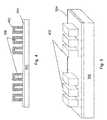
FIG. 1 , illustrated is an embodiment of a method of fabricating a Ge-FinFET element. The method begins atstep 102 where a substrate including one or more fins is provided. In an embodiment, the substrate includes a silicon substrate (e.g., wafer). The substrate may be silicon in a crystalline structure. In other embodiments, the substrate may include other elementary semiconductors such as germanium, or include a compound semiconductor such as, silicon carbide, gallium arsenide, indium arsenide, and indium phosphide. In an embodiment, the substrate includes a silicon-on-insulator (SOI) substrate. The SOI substrate may be fabricated using separation by implantation of oxygen (SIMOX), wafer bonding, and/or other suitable methods. In an embodiment, the fins are silicon fins (Si-fins). The fins may be formed, for example, by etching a layer of silicon on the substrate. The layer of silicon may be a silicon layer of an SOI substrate (e.g., overlying an insulator layer). - Referring to the example of
FIGS. 2 and 3 , asubstrate 202 is provided. Thesubstrate 202 may include silicon. Aninsulator layer 204 is disposed on thesubstrate 202. Thesubstrate 202 and theinsulator layer 204 may be components of an SOI substrate (e.g., including an overlying silicon layer patterned to form fins206). Theinsulator layer 204 may include silicon oxide, sapphire, and/or other suitable insulating materials. Theinsulator layer 204 may be a buried oxide layer (BOX). A plurality offins 206 is disposed on theinsulator layer 204. In an embodiment, the plurality offins 206 includes silicon. The plurality offins 206 may be fabricated by patterning a silicon layer overlying the insulator layer204 (e.g., an upper silicon layer of a silicon-insulator-silicon stack of an SOI substrate). Thefins 206 may include a capping layer disposed on the fin. In an embodiment, the capping layer is a silicon layer. - The
fins 206 may be fabricated using suitable processes including photolithography and etch processes. The photolithography process may include forming a photoresist layer (resist) overlying the substrate (e.g., on a silicon layer), exposing the resist to a pattern, performing post-exposure bake processes, and developing the resist to form a masking element including the resist. The masking element may then be used to etchfins 206 into the silicon layer. Thefins 206 may be etched using reactive ion etch (RIE) and/or other suitable processes. - In an embodiment, the
fins 206 are formed by double-patterning lithography (DPL) process. DPL is a method of constructing a pattern on a substrate by dividing the pattern into two interleaved patterns. DPL allows enhanced feature (e.g., fin) density. Various DPL methodologies may used including, double exposure (e.g., using two mask sets), forming spacers adjacent features and removing the features to provide a pattern of spacers, resist freezing, and/or other suitable processes. - The
method 100 then proceeds to step104 where a layer including germanium is formed on each of the fins. The layer may include an epitaxial layer grown on the fins. The epitaxial layer may include SiGe. The epitaxial layer may be grown by a CMOS compatible epitaxial process. The epitaxial process may include chemical vapor deposition (CVD) technique such as vapor-phase epitaxy (VPE), and/or other suitable processes known in the art. The epitaxial process may use gaseous (or liquid) precursors, which interact with composition of the fins (e.g., silicon). In an embodiment, a low germanium concentration Si1-xGex, where x is between approximately 0.1 and 0.3, is provided. Referring to the example ofFIGS. 4 and 5 , anepitaxial layer 402 is grown on thefins 206. In an embodiment, thefins 206 are silicon and anepitaxial layer 402 includes SiGe. In an embodiment, theepitaxial layer 402 includes a low Ge concentration (e.g., Si1-xGexwhere x is between approximately 0.1 and 0.3). - The
method 100 then proceeds to step106 where a germanium condensation process (Ge-condensation) is performed. The germanium condensation process transforms the fins provided instep 102, to fins including germanium (Ge-fins). In an embodiment, the Ge-condensation process transforms silicon fins to Ge-fins. It should be noted that the term Ge-fin as provided herein does not necessitate a fin of exclusively germanium (e.g., pure germanium). - The Ge-condensation process includes selectively oxidizing the layer including germanium and/or fins, described above with reference to
steps step 106 provides for the transforming of Si-fins to Ge-fins. - Referring to the example of
FIGS. 6 and 7 ,fins 602 are formed. Thefins 602 include germanium (e.g., Ge-fins). Anoxidized layer 604 is formed around thefins 602. The oxidized layer includes silicon oxide. The oxidizedlayer 604 may be formed by oxidation. For example, during an oxidation process silicon of theepitaxial layer 402 and/of thefins 206, illustrated onFIGS. 4 and 5 , may be consumed and form the oxidizedlayer 604. As the silicon is consumed, germanium from theepi layer 402 is transferred to the center of the structure to formfins 602. - The
method 100 then proceeds to step108 where the oxidized layer (e.g., formed by the Ge-condensation process) is removed from the substrate. The oxidized layer may be removed by suitable etching processes including wet etch, dry etch, plasma etch, and/or other suitable processes. In an embodiment, a wet etch including a diluted hydrofluoric acid (dHF) solution is used to remove the oxidized layer. The etching process may also remove a portion of the underlying insulator layer. Thus, a recess in the underlying insulator layer may be formed. Referring to the example ofFIGS. 8 and 9 , the oxidizedlayer 604 has been removed exposing the Ge-fins 602. The removal of the oxidizedlayer 604 createsrecesses 802 in theinsulator layer 204. Thus, afin structure 806 is formed including an upper portion including Ge-fins 602 and a lower portion including aninsulator portion 804. Theinsulator portion 804 is raised from the substrate (e.g., forms a fin) due therecesses 802. A channel of a FinFET device may be formed in the upper portion of thefin structure 806. - The
method 100 may continue to provides steps fabricating other features of FinFET elements, including, for example, doping the fin structure, forming a gate structure including a gate dielectric and gate electrode on the fins, forming of source/drain regions, forming contact, interconnect structures, and/or other suitable processes and features. - Therefore, provided is a
method 100 for forming a FinFET element having fins including germanium (e.g., Ge-fin) on a substrate. Themethod 100 uses CMOS compatible processes. Themethod 100 also allows for use of an SOI substrate. This removes the need to provide a germanium on insulator (GOI) substrate, which may provide issues in fabrication. - Referring to
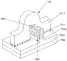
FIG. 10 , illustrated is an embodiment of a FinFET element1000. The FinFET element1000 may be formed using themethod 100, described above with reference toFIG. 1 , or a portion thereof. The FinFET element1000 includes asubstrate 1002, aninsulator layer 1004, afin structure 1006, and agate structure 1010. In an embodiment, thesubstrate 1002 includes a silicon substrate. Thesubstrate 1002 may be silicon in a crystalline structure. In other embodiments, thesubstrate 1002 may include other elementary semiconductors such as germanium, or include a compound semiconductor such as, silicon carbide, gallium arsenide, indium arsenide, and indium phosphide. In an embodiment, thesubstrate 1002 includes a silicon-on-insulator (SOI) substrate. The SOI substrate may be fabricated using separation by implantation of oxygen (SIMOX), wafer bonding, and/or other suitable methods. Thesubstrate 1002 may include isolation regions, doped regions, and/or other features. - The
insulator layer 1004 is disposed on thesubstrate 1002. Theinsulator layer 1004 may include silicon. In an embodiment, theinsulator layer 1004 is silicon oxide. Theinsulator layer 1004 may be a buried oxide (BOX) layer. Theinsulator layer 1004 may be a component (e.g., layer) of an SOI substrate. Theinsulator layer 1004 may be formed using processes such as, implantation (e.g., SIMOX), oxidation, deposition, and/or suitable processes. Theinsulator layer 1004 includes a raised portion (fin)1004athat is included in thefin structure 1006. Theinsulator fin portion 1004amay be formed by an etching process used to provide a Ge-fin 1008 of thefin structure 1006, for example, as described above with reference to step108 ofFIG. 1 . - The
fin structure 1006 includes an upper portion including the Ge-fin 1008 and a lower portion including theinsulator fin portion 1004a. The Ge-fin 1008 may be formed by processes including providing a silicon-fin, growing a layer including germanium on the silicon-fin, and using a Ge-condensation process to provide Ge-fins. The Ge-fin 1008 may be formed using themethod 100, or portion thereof. - The
gate structure 1010 is formed on thefin structure 1008. Thegate structure 1010 includes agate dielectric layer 1014 and agate electrode 1012. Numerous other layers may also be present, for example, capping layers, interface layers, spacer elements, and/or other suitable features. Thegate dielectric layer 1014 may include dielectric material such as, silicon oxide, silicon nitride, silicon oxinitride, dielectric with a high dielectric constant (high k), and/or combinations thereof. Examples of high k materials include hafnium silicate, hafnium oxide, zirconium oxide, aluminum oxide, hafnium dioxide-alumina (HfO2—Al2O3) alloy, and/or combinations thereof. Thegate dielectric layer 1014 may be formed using processes such as, photolithography patterning, oxidation, deposition, etching, and/or other suitable processes. Thegate electrode 1012 may include polysilicon, silicon-germanium, a metal including metal compounds such as, Mo, Cu, W, Ti, Ta, TiN, TaN, NiSi, CoSi, and/or other suitable conductive materials known in the art. Thegate electrode 1012 may be formed using processes such as, physical vapor deposition (PVD), chemical vapor deposition (CVD), plasma-enhanced chemical vapor deposition (PECVD), atmospheric pressure chemical vapor deposition (APCVD), low-pressure CVD (LPCVD), high density plasma CVD (HD CVD), atomic layer CVD (ALCVD), and/or other suitable processes which may be followed, for example, by photolithography and/or etching processes. - The
fin structure 1008, and in particular the upper portion including the Ge-fin 1008 may include a channel of theFinFET element 100. Thefin structure 1006 may be doped to provide a suitable channel for an N-FinFET (NMOS device) or P-FinFET (PMOS device). Thefin structure 1006, and in particular the upper portion including the Ge-fin 1008, may include suitable dopants such as, p-type dopants (e.g., boron) and/or n-type dopants (e.g., phosphorous). Thefin structure 1006 may be doped using processes such as, ion implantation, diffusion, annealing, and/or other suitable processes. - The
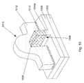
fin structure 1008 may include and/or be coupled to source and drain regions associated with the FinFET element1000. The FinFET device including the FinFET element1000 may be a device included in a microprocessor, memory cell, and/or other semiconductor devices. - Referring now to
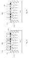
FIGS. 11 ,12,13, and14 illustrated are examples of an embodiment of the method ofFIG. 1 . The examples ofFIGS. 11 ,12,13, and14 include a bulk silicon substrate and include many of the same or substantially similar steps as described above with reference toFIG. 1 and the examples ofFIGS. 2-9 . Referring to the example ofFIG. 11 , asubstrate 1102 is provided. Thesubstrate 1102 may be silicon in crystalline structure (e.g., a bulk silicon substrate). Fins1104 (e.g., Si-fins) extend from thesubstrate 1102. Thefins 1104 include silicon. Thefins 1104 may be fabricated by using suitable process such as photolithography and etch. In an embodiment, thefins 1104 are etched from thesubstrate 1102 using dry etch or plasma processes. Shallow trench isolation (STI)structures 1106 surround thefins 1104. TheSTI structures 1106 may include any suitable insulating material. - Referring to the example of
FIG. 12 , illustrated is an embodiment ofstep 104 of themethod 100, described above with reference toFIG. 1 . Alayer 1202 is provided on thefins 1104. Thelayer 1202 includes germanium. In an embodiment, thelayer 1202 is Si1-xGex, which may be substantially similar to as described above with reference to epitaxial layer described above with reference to step104. In an embodiment, thelayer 1202 is epitaxially grown. - Referring to the example of
FIG. 13 , illustrated is an embodiment of thestep 106 of themethod 100 using a bulk silicon substrate. A germanium condensation process is performed which forms Ge-fins 1302 with a silicon oxide layer (e.g., cap layer)1304. In addition, a portion of thesilicon fin 1104 is oxidized during the condensation process. This forms theoxidized segment 1306. The oxidizedsegments 1306 include silicon oxide. The germanium condensation process may be substantially similar to as described above with reference toFIG. 1 . - Referring to the example of
FIG. 14 , an embodiment of thestep 108 of themethod 100 using a bulk silicon substrate is illustrated. In an embodiment, thecap layer 1304 is removed by a suitable wet etch process, however, other embodiments maybe possible. The oxidizedsegments 1306 may not be removed. Note that the Ge-fins 1302 are isolated from the remaining portion of the Si-fins 1104 by the oxidized segment1306 (e.g., silicon oxide insulator). - The embodiment of the method may continue to form transistor features such as gate, source, and drains on or adjacent the formed Ge-
fins 1302. One or more of these features is described in detail with reference toFIG. 10 . Therefore, provided is a method of forming a Ge-FinFET element from a bulk silicon substrate. - Although only a few exemplary embodiments of this invention have been described in detail above, those skilled in the art will readily appreciate that many modifications are possible in the exemplary embodiments without material departing from the novel teachings and advantages of this disclosure.
Claims (21)
Priority Applications (3)
| Application Number | Priority Date | Filing Date | Title |
|---|---|---|---|
| US12/425,854US8053299B2 (en) | 2009-04-17 | 2009-04-17 | Method of fabrication of a FinFET element |
| CN200910209143ACN101866885A (en) | 2009-04-17 | 2009-10-28 | Manufacturing method of FINFET element |
| US13/247,507US8648400B2 (en) | 2009-04-17 | 2011-09-28 | FinFET semiconductor device with germanium (GE) fins |
Applications Claiming Priority (1)
| Application Number | Priority Date | Filing Date | Title |
|---|---|---|---|
| US12/425,854US8053299B2 (en) | 2009-04-17 | 2009-04-17 | Method of fabrication of a FinFET element |
Related Child Applications (1)
| Application Number | Title | Priority Date | Filing Date |
|---|---|---|---|
| US13/247,507DivisionUS8648400B2 (en) | 2009-04-17 | 2011-09-28 | FinFET semiconductor device with germanium (GE) fins |
Publications (2)
| Publication Number | Publication Date |
|---|---|
| US20100264468A1true US20100264468A1 (en) | 2010-10-21 |
| US8053299B2 US8053299B2 (en) | 2011-11-08 |
Family
ID=42958533
Family Applications (2)
| Application Number | Title | Priority Date | Filing Date |
|---|---|---|---|
| US12/425,854Expired - Fee RelatedUS8053299B2 (en) | 2009-04-17 | 2009-04-17 | Method of fabrication of a FinFET element |
| US13/247,507ActiveUS8648400B2 (en) | 2009-04-17 | 2011-09-28 | FinFET semiconductor device with germanium (GE) fins |
Family Applications After (1)
| Application Number | Title | Priority Date | Filing Date |
|---|---|---|---|
| US13/247,507ActiveUS8648400B2 (en) | 2009-04-17 | 2011-09-28 | FinFET semiconductor device with germanium (GE) fins |
Country Status (2)
| Country | Link |
|---|---|
| US (2) | US8053299B2 (en) |
| CN (1) | CN101866885A (en) |
Cited By (92)
| Publication number | Priority date | Publication date | Assignee | Title |
|---|---|---|---|---|
| US20070228372A1 (en)* | 2004-10-19 | 2007-10-04 | Taiwan Semiconductor Manufacturing Company, Ltd. | Method for Fabricating a Body Contact in a Finfet Structure and a Device Including the Same |
| US20090035909A1 (en)* | 2007-07-31 | 2009-02-05 | Taiwan Semiconductor Manufacturing Company, Ltd. | Method of fabrication of a finfet element |
| US20100006945A1 (en)* | 2008-06-11 | 2010-01-14 | Taiwan Semiconductor Manufacturing Company, Ltd. | Finfet drive strength modification |
| US20100052059A1 (en)* | 2008-08-28 | 2010-03-04 | Taiwan Semiconductor Manufacturing Company, Ltd. | Finfet process compatible native transistor |
| US20100187622A1 (en)* | 2008-03-13 | 2010-07-29 | Tela Innovations, Inc. | Linear Gate Level Cross-Coupled Transistor Device with Complimentary Pairs of Cross-Coupled Transistors Defined by Physically Separate Gate Electrodes within Gate Electrode Level |
| US20100203734A1 (en)* | 2009-02-12 | 2010-08-12 | Taiwan Semiconductor Manufacturing Company, Ltd. | Method of pitch halving |
| US20100287518A1 (en)* | 2009-05-06 | 2010-11-11 | Tela Innovations, Inc. | Cell Circuit and Layout with Linear Finfet Structures |
| US20100292963A1 (en)* | 2009-04-15 | 2010-11-18 | James Schroeder | Personal fit medical implants and orthopedic surgical instruments and methods for making |
| US20100296213A1 (en)* | 2009-02-19 | 2010-11-25 | Jam-Wem Lee | ESD Protection for FinFETs |
| US20110003469A1 (en)* | 2009-07-02 | 2011-01-06 | Kewley David A | Methods Of Forming Memory Cells; And Methods Of Forming Vertical Structures |
| US20110068407A1 (en)* | 2009-09-24 | 2011-03-24 | Taiwan Semiconductor Manufacturing Company, Ltd. | Germanium FinFETs with Metal Gates and Stressors |
| US20110101421A1 (en)* | 2009-10-30 | 2011-05-05 | Taiwan Semiconductor Manufacturing Company, Ltd. | Method of forming epi film in substrate trench |
| US20110117679A1 (en)* | 2009-11-19 | 2011-05-19 | Taiwan Semiconductor Manufacturing Company, Ltd. | Sacrificial offset protection film for a finfet device |
| US20110151359A1 (en)* | 2009-01-20 | 2011-06-23 | Taiwan Semiconductor Manufacturing Company, Ltd. | Integrated circuit layout design |
| US20110147846A1 (en)* | 2009-12-22 | 2011-06-23 | Taiwan Semiconductor Manufacturing Company, Ltd | Method for incorporating impurity element in epi silicon process |
| US20110193141A1 (en)* | 2010-02-11 | 2011-08-11 | Taiwan Semiconductor Manufacturing Company, Ltd. | Method of fabricating a finfet device |
| US8062963B1 (en) | 2010-10-08 | 2011-11-22 | Taiwan Semiconductor Manufacturing Company, Ltd. | Method of fabricating a semiconductor device having an epitaxy region |
| US8214778B2 (en) | 2007-08-02 | 2012-07-03 | Tela Innovations, Inc. | Methods for cell phasing and placement in dynamic array architecture and implementation of the same |
| US8212295B2 (en) | 2010-06-30 | 2012-07-03 | Taiwan Semiconductor Manufacturing Company, Ltd. | ROM cell circuit for FinFET devices |
| US8225239B2 (en) | 2006-03-09 | 2012-07-17 | Tela Innovations, Inc. | Methods for defining and utilizing sub-resolution features in linear topology |
| US8225261B2 (en) | 2006-03-09 | 2012-07-17 | Tela Innovations, Inc. | Methods for defining contact grid in dynamic array architecture |
| US8245180B2 (en) | 2006-03-09 | 2012-08-14 | Tela Innovations, Inc. | Methods for defining and using co-optimized nanopatterns for integrated circuit design and apparatus implementing same |
| US8247846B2 (en) | 2006-03-09 | 2012-08-21 | Tela Innovations, Inc. | Oversized contacts and vias in semiconductor chip defined by linearly constrained topology |
| US8253173B2 (en) | 2006-03-09 | 2012-08-28 | Tela Innovations, Inc. | Semiconductor device with gate level including four transistors of first type and four transistors of second type separated by non-diffusion region and having at least two gate contacts positioned outside separating non-diffusion region |
| US8278173B2 (en) | 2010-06-30 | 2012-10-02 | Taiwan Semiconductor Manufacturing Company, Ltd. | Method of fabricating gate structures |
| US8278196B2 (en) | 2010-07-21 | 2012-10-02 | Taiwan Semiconductor Manufacturing Company, Ltd. | High surface dopant concentration semiconductor device and method of fabricating |
| US8283701B2 (en) | 2007-08-02 | 2012-10-09 | Tela Innovations, Inc. | Semiconductor device with dynamic array sections defined and placed according to manufacturing assurance halos |
| US8286107B2 (en) | 2007-02-20 | 2012-10-09 | Tela Innovations, Inc. | Methods and systems for process compensation technique acceleration |
| US8286114B2 (en) | 2007-04-18 | 2012-10-09 | Taiwan Semiconductor Manufacturing Company, Ltd. | 3-dimensional device design layout |
| US8338305B2 (en) | 2010-10-19 | 2012-12-25 | Taiwan Semiconductor Manufacturing Company, Ltd. | Multi-fin device by self-aligned castle fin formation |
| US8357569B2 (en) | 2009-09-29 | 2013-01-22 | Taiwan Semiconductor Manufacturing Company, Ltd. | Method of fabricating finfet device |
| US8367498B2 (en) | 2010-10-18 | 2013-02-05 | Taiwan Semiconductor Manufacturing Company, Ltd. | Fin-like field effect transistor (FinFET) device and method of manufacturing same |
| US8373229B2 (en) | 2010-08-30 | 2013-02-12 | Taiwan Semiconductor Manufacturing Company, Ltd. | Gate controlled bipolar junction transistor on fin-like field effect transistor (FinFET) structure |
| US8399931B2 (en) | 2010-06-30 | 2013-03-19 | Taiwan Semiconductor Manufacturing Company, Ltd. | Layout for multiple-fin SRAM cell |
| US8448102B2 (en) | 2006-03-09 | 2013-05-21 | Tela Innovations, Inc. | Optimizing layout of irregular structures in regular layout context |
| US8453094B2 (en) | 2008-01-31 | 2013-05-28 | Tela Innovations, Inc. | Enforcement of semiconductor structure regularity for localized transistors and interconnect |
| US8471391B2 (en) | 2008-03-27 | 2013-06-25 | Tela Innovations, Inc. | Methods for multi-wire routing and apparatus implementing same |
| US8486769B2 (en) | 2010-11-19 | 2013-07-16 | Taiwan Semiconductor Manufacturing Company, Ltd. | Method for forming metrology structures from fins in integrated circuitry |
| US8525267B2 (en) | 2010-11-23 | 2013-09-03 | Taiwan Semiconductor Manufacturing Company, Ltd. | Device and method for forming Fins in integrated circuitry |
| US8541879B2 (en) | 2007-12-13 | 2013-09-24 | Tela Innovations, Inc. | Super-self-aligned contacts and method for making the same |
| US8609495B2 (en) | 2010-04-08 | 2013-12-17 | Taiwan Semiconductor Manufacturing Company, Ltd. | Hybrid gate process for fabricating finfet device |
| US8621398B2 (en) | 2010-05-14 | 2013-12-31 | Taiwan Semiconductor Manufacturing Company, Ltd. | Automatic layout conversion for FinFET device |
| US8633076B2 (en) | 2010-11-23 | 2014-01-21 | Taiwan Semiconductor Manufacturing Company, Ltd. | Method for adjusting fin width in integrated circuitry |
| US8653857B2 (en) | 2006-03-09 | 2014-02-18 | Tela Innovations, Inc. | Circuitry and layouts for XOR and XNOR logic |
| US8661392B2 (en) | 2009-10-13 | 2014-02-25 | Tela Innovations, Inc. | Methods for cell boundary encroachment and layouts implementing the Same |
| US8658542B2 (en) | 2006-03-09 | 2014-02-25 | Tela Innovations, Inc. | Coarse grid design methods and structures |
| US8667443B2 (en) | 2007-03-05 | 2014-03-04 | Tela Innovations, Inc. | Integrated circuit cell library for multiple patterning |
| US8675397B2 (en) | 2010-06-25 | 2014-03-18 | Taiwan Semiconductor Manufacturing Company, Ltd. | Cell structure for dual-port SRAM |
| US8680626B2 (en) | 2007-10-26 | 2014-03-25 | Tela Innovations, Inc. | Methods, structures, and designs for self-aligning local interconnects used in integrated circuits |
| US8716094B1 (en)* | 2012-11-21 | 2014-05-06 | Global Foundries Inc. | FinFET formation using double patterning memorization |
| US8729627B2 (en) | 2010-05-14 | 2014-05-20 | Taiwan Semiconductor Manufacturing Company, Ltd. | Strained channel integrated circuit devices |
| US20140197457A1 (en)* | 2013-01-14 | 2014-07-17 | Taiwan Semiconductor Manufacturing Company Ltd. | FinFET Device and Method of Fabricating Same |
| US8785284B1 (en)* | 2013-02-20 | 2014-07-22 | International Business Machines Corporation | FinFETs and fin isolation structures |
| US8796156B2 (en) | 2009-10-27 | 2014-08-05 | Taiwan Semiconductor Manufacturing Company, Ltd. | Cross OD FinFET patterning |
| US8796759B2 (en) | 2010-07-15 | 2014-08-05 | Taiwan Semiconductor Manufacturing Company, Ltd. | Fin-like field effect transistor (FinFET) device and method of manufacturing same |
| US8796124B2 (en) | 2011-10-25 | 2014-08-05 | Taiwan Semiconductor Manufacturing Company, Ltd. | Doping method in 3D semiconductor device |
| US8828839B2 (en)* | 2013-01-29 | 2014-09-09 | GlobalFoundries, Inc. | Methods for fabricating electrically-isolated finFET semiconductor devices |
| US8828818B1 (en) | 2013-03-13 | 2014-09-09 | Samsung Electronics Co., Ltd. | Methods of fabricating integrated circuit device with fin transistors having different threshold voltages |
| US8839175B2 (en) | 2006-03-09 | 2014-09-16 | Tela Innovations, Inc. | Scalable meta-data objects |
| US8863063B2 (en) | 2009-05-06 | 2014-10-14 | Tela Innovations, Inc. | Finfet transistor circuit |
| US8881084B2 (en) | 2010-05-14 | 2014-11-04 | Taiwan Semiconductor Manufacturing Company, Ltd. | FinFET boundary optimization |
| KR20140133727A (en)* | 2013-05-10 | 2014-11-20 | 삼성전자주식회사 | Semiconductor device and method of manufacturing the same |
| US8942030B2 (en) | 2010-06-25 | 2015-01-27 | Taiwan Semiconductor Manufacturing Company, Ltd. | Structure and method for SRAM cell circuit |
| JP2015508567A (en)* | 2011-12-16 | 2015-03-19 | インターナショナル・ビジネス・マシーンズ・コーポレーションInternational Business Machines Corporation | Semiconductor structure and manufacturing method thereof (rare earth oxide separation type semiconductor fin) |
| US9035359B2 (en) | 2006-03-09 | 2015-05-19 | Tela Innovations, Inc. | Semiconductor chip including region including linear-shaped conductive structures forming gate electrodes and having electrical connection areas arranged relative to inner region between transistors of different types and associated methods |
| WO2015102884A1 (en)* | 2014-01-03 | 2015-07-09 | Qualcomm Incorporated | Silicon germanium finfet formation by ge condensation |
| US9122832B2 (en) | 2008-08-01 | 2015-09-01 | Tela Innovations, Inc. | Methods for controlling microloading variation in semiconductor wafer layout and fabrication |
| US9130058B2 (en) | 2010-07-26 | 2015-09-08 | Taiwan Semiconductor Manufacturing Company, Ltd. | Forming crown active regions for FinFETs |
| US20150287721A1 (en)* | 2012-08-29 | 2015-10-08 | International Business Machines Corporation | Sublithographic width finfet employing solid phase epitaxy |
| US9159627B2 (en) | 2010-11-12 | 2015-10-13 | Tela Innovations, Inc. | Methods for linewidth modification and apparatus implementing the same |
| US9166022B2 (en) | 2010-10-18 | 2015-10-20 | Taiwan Semiconductor Manufacturing Company, Ltd. | Fin-like field effect transistor (FinFET) device and method of manufacturing same |
| US9230910B2 (en) | 2006-03-09 | 2016-01-05 | Tela Innovations, Inc. | Oversized contacts and vias in layout defined by linearly constrained topology |
| US9263528B2 (en) | 2012-10-05 | 2016-02-16 | Imec | Method for producing strained Ge fin structures |
| US9269629B2 (en)* | 2012-11-26 | 2016-02-23 | Globalfoundries Inc. | Dummy fin formation by gas cluster ion beam |
| US20160211262A1 (en)* | 2013-09-25 | 2016-07-21 | Walid M. Hafez | Isolation well doping with solid-state diffusion sources for finfet architectures |
| US20160240675A1 (en)* | 2012-01-23 | 2016-08-18 | Taiwan Semiconductor Manufacturing Company, Ltd. | Structure and method for transistors with line end extension |
| US9472550B2 (en) | 2010-11-23 | 2016-10-18 | Taiwan Semiconductor Manufacturing Company, Ltd. | Adjusted fin width in integrated circuitry |
| US9607987B2 (en) | 2011-12-21 | 2017-03-28 | Intel Corporation | Methods for forming fins for metal oxide semiconductor device structures |
| US9685439B1 (en)* | 2016-05-02 | 2017-06-20 | Taiwan Semiconductor Manufacturing Co., Ltd. | Semiconductor device and manufacturing method thereof |
| US9698058B2 (en) | 2014-04-25 | 2017-07-04 | Taiwan Semiconductor Manufacturing Company, Ltd. | Structure and method for FinFET device |
| US9716176B2 (en) | 2013-11-26 | 2017-07-25 | Samsung Electronics Co., Ltd. | FinFET semiconductor devices including recessed source-drain regions on a bottom semiconductor layer and methods of fabricating the same |
| US9721955B2 (en) | 2014-04-25 | 2017-08-01 | Taiwan Semiconductor Manufacturing Company, Ltd. | Structure and method for SRAM FinFET device having an oxide feature |
| US20170338237A1 (en)* | 2016-05-19 | 2017-11-23 | Taiwan Semiconductor Manufacturing Co., Ltd. | Method of fabricating non-volatile memory device array |
| TWI616931B (en)* | 2013-10-21 | 2018-03-01 | 三星電子股份有限公司 | Method of fabricating semiconductor device and method of forming patterns |
| US10468528B2 (en) | 2014-04-16 | 2019-11-05 | Taiwan Semiconductor Manufacturing Company, Ltd. | FinFET device with high-k metal gate stack |
| AU2018200549B2 (en)* | 2012-01-13 | 2019-12-05 | Tela Innovations, Inc. | Circuits with linear finfet structures |
| US11205594B2 (en) | 2013-01-14 | 2021-12-21 | Taiwan Semiconductor Manufacturing Company, Ltd. | Fin spacer protected source and drain regions in FinFETs |
| US11222947B2 (en) | 2015-09-25 | 2022-01-11 | Intel Corporation | Methods of doping fin structures of non-planar transistor devices |
| DE112011105979B4 (en) | 2011-12-20 | 2022-09-15 | Intel Corporation | Semiconductor device with isolated semiconductor body parts and manufacturing method |
| US11563118B2 (en) | 2014-06-27 | 2023-01-24 | Taiwan Semiconductor Manufacturing Company, Ltd. | Structure and method for SRAM FinFET device |
| US11735668B2 (en)* | 2018-06-11 | 2023-08-22 | Taiwan Semiconductor Manufacturing Company, Ltd. | Interfacial layer between fin and source/drain region |
| US12218239B2 (en) | 2012-01-23 | 2025-02-04 | Mosaid Technologies Incorporated | Structure and method for providing line end extensions for fin-type active regions |
Families Citing this family (127)
| Publication number | Priority date | Publication date | Assignee | Title |
|---|---|---|---|---|
| CN102956686A (en)* | 2011-08-18 | 2013-03-06 | 中国科学院微电子研究所 | Silicon-based germanium nano-structure substrate and preparation method thereof |
| CN103165455B (en)* | 2011-12-13 | 2015-09-09 | 中芯国际集成电路制造(上海)有限公司 | Make the method for fin-shaped field effect transistor |
| US8486770B1 (en)* | 2011-12-30 | 2013-07-16 | Taiwan Semiconductor Manufacturing Company, Ltd. | Method of forming CMOS FinFET device |
| US9117877B2 (en) | 2012-01-16 | 2015-08-25 | Globalfoundries Inc. | Methods of forming a dielectric cap layer on a metal gate structure |
| US9281378B2 (en) | 2012-01-24 | 2016-03-08 | Taiwan Semiconductor Manufacturing Company, Ltd. | Fin recess last process for FinFET fabrication |
| US9171925B2 (en) | 2012-01-24 | 2015-10-27 | Taiwan Semiconductor Manufacturing Company, Ltd. | Multi-gate devices with replaced-channels and methods for forming the same |
| US9466696B2 (en) | 2012-01-24 | 2016-10-11 | Taiwan Semiconductor Manufacturing Company, Ltd. | FinFETs and methods for forming the same |
| US8694938B2 (en) | 2012-06-27 | 2014-04-08 | Taiwan Semiconductor Manufacturing Company Limited | Discrete device modeling |
| CN102738060B (en)* | 2012-07-02 | 2014-04-23 | 中国科学院上海微系统与信息技术研究所 | A kind of preparation method of GOI wafer structure |
| US8963206B2 (en) | 2012-08-27 | 2015-02-24 | Taiwan Semiconductor Manufacturing Co., Ltd. | Method for increasing fin density |
| CN103681447A (en)* | 2012-09-10 | 2014-03-26 | 中国科学院微电子研究所 | SOI substrate manufacturing method and SOI substrate |
| US9443962B2 (en) | 2012-11-09 | 2016-09-13 | Taiwan Semiconductor Manufacturing Company, Ltd. | Recessing STI to increase fin height in fin-first process |
| US9349837B2 (en) | 2012-11-09 | 2016-05-24 | Taiwan Semiconductor Manufacturing Company, Ltd. | Recessing STI to increase Fin height in Fin-first process |
| CN103811325B (en)* | 2012-11-13 | 2016-12-21 | 中芯国际集成电路制造(上海)有限公司 | The forming method of fin field effect pipe |
| CN103219381B (en)* | 2013-01-16 | 2016-03-30 | 南京大学 | Ge base tri-gate devices and manufacture method |
| US8963259B2 (en) | 2013-05-31 | 2015-02-24 | Globalfoundries Inc. | Device isolation in finFET CMOS |
| US9349850B2 (en)* | 2013-07-17 | 2016-05-24 | Taiwan Semiconductor Manufacturing Company, Ltd. | Thermally tuning strain in semiconductor devices |
| US9553012B2 (en) | 2013-09-13 | 2017-01-24 | Taiwan Semiconductor Manufacturing Company Ltd. | Semiconductor structure and the manufacturing method thereof |
| US9583590B2 (en) | 2013-09-27 | 2017-02-28 | Samsung Electronics Co., Ltd. | Integrated circuit devices including FinFETs and methods of forming the same |
| US9178045B2 (en) | 2013-09-27 | 2015-11-03 | Samsung Electronics Co., Ltd. | Integrated circuit devices including FinFETS and methods of forming the same |
| CN105493251A (en)* | 2013-09-27 | 2016-04-13 | 英特尔公司 | Non-planar semiconductor device with multi-layer flexible substrate |
| US9425042B2 (en) | 2013-10-10 | 2016-08-23 | Taiwan Semiconductor Manufacturing Company Limited | Hybrid silicon germanium substrate for device fabrication |
| CN104658908A (en)* | 2013-11-18 | 2015-05-27 | 中芯国际集成电路制造(上海)有限公司 | Method for manufacturing FinFET |
| US9425257B2 (en) | 2013-11-20 | 2016-08-23 | Taiwan Semiconductor Manufacturing Company Limited | Non-planar SiGe channel PFET |
| US9159552B2 (en) | 2013-12-27 | 2015-10-13 | Taiwan Semiconductor Manufacturing Company, Ltd. | Method of forming a germanium-containing FinFET |
| WO2015127701A1 (en)* | 2014-02-25 | 2015-09-03 | Tsinghua University | Method for forming fin field effect transistor |
| US9548303B2 (en) | 2014-03-13 | 2017-01-17 | Taiwan Semiconductor Manufacturing Company, Ltd. | FinFET devices with unique fin shape and the fabrication thereof |
| US9780216B2 (en)* | 2014-03-19 | 2017-10-03 | Taiwan Semiconductor Manufacturing Company, Ltd. | Combination FinFET and methods of forming same |
| US9299780B2 (en) | 2014-03-26 | 2016-03-29 | International Business Machines Corporation | Constrained epitaxial source/drain regions on semiconductor-on-insulator finFET device |
| US9362362B2 (en)* | 2014-04-09 | 2016-06-07 | International Business Machines Corporation | FinFET with dielectric isolated channel |
| US9293375B2 (en) | 2014-04-24 | 2016-03-22 | International Business Machines Corporation | Selectively grown self-aligned fins for deep isolation integration |
| US9536900B2 (en) | 2014-05-22 | 2017-01-03 | Globalfoundries Inc. | Forming fins of different semiconductor materials on the same substrate |
| US9312364B2 (en) | 2014-05-27 | 2016-04-12 | International Business Machines Corporation | finFET with dielectric isolation after gate module for improved source and drain region epitaxial growth |
| KR20160004097A (en)* | 2014-07-02 | 2016-01-12 | 삼성전자주식회사 | Fin structure and fabrication method thereof, and fin transistor and fabrication method thereof using the same |
| US9147616B1 (en)* | 2014-08-28 | 2015-09-29 | Globalfoundries Inc. | Methods of forming isolated fins for a FinFET semiconductor device with alternative channel materials |
| KR102241974B1 (en) | 2014-09-23 | 2021-04-19 | 삼성전자주식회사 | Semiconductor devices and methods of manufacturing the same |
| US9391201B2 (en) | 2014-11-25 | 2016-07-12 | Taiwan Semiconductor Manufacturing Company, Ltd. | Source/drain structure and manufacturing the same |
| US9349652B1 (en) | 2014-12-12 | 2016-05-24 | Taiwan Semiconductor Manufacturing Company, Ltd. | Method of forming semiconductor device with different threshold voltages |
| US9741811B2 (en) | 2014-12-15 | 2017-08-22 | Samsung Electronics Co., Ltd. | Integrated circuit devices including source/drain extension regions and methods of forming the same |
| US9780214B2 (en) | 2014-12-22 | 2017-10-03 | Taiwan Semiconductor Manufacturing Co., Ltd. | Semiconductor device including Fin- FET and manufacturing method thereof |
| US10134871B2 (en) | 2014-12-23 | 2018-11-20 | Taiwan Semiconductor Manufacturing Company, Ltd. | Doping of high-K dielectric oxide by wet chemical treatment |
| US10141310B2 (en) | 2014-12-23 | 2018-11-27 | Taiwan Semiconductor Manufacturing Company, Ltd. | Short channel effect suppression |
| US9768301B2 (en) | 2014-12-23 | 2017-09-19 | Taiwan Semiconductor Manufacturing Company, Ltd. | Short channel effect suppression |
| US9515071B2 (en) | 2014-12-24 | 2016-12-06 | Taiwan Semiconductor Manufacturing Company, Ltd. | Asymmetric source/drain depths |
| US9614057B2 (en) | 2014-12-30 | 2017-04-04 | International Business Machines Corporation | Enriched, high mobility strained fin having bottom dielectric isolation |
| US9425250B2 (en) | 2014-12-30 | 2016-08-23 | Taiwan Semiconductor Manufacturing Company, Ltd. | Transistor with wurtzite channel |
| US9647090B2 (en) | 2014-12-30 | 2017-05-09 | Taiwan Semiconductor Manufacturing Company, Ltd. | Surface passivation for germanium-based semiconductor structure |
| US9472573B2 (en) | 2014-12-30 | 2016-10-18 | International Business Machines Corporation | Silicon-germanium fin formation |
| US9601626B2 (en) | 2015-01-23 | 2017-03-21 | Taiwan Semiconductor Manufacturing Co., Ltd. | Semiconductor device including fin structure with two channel layers and manufacturing method thereof |
| CN106158632B (en)* | 2015-03-26 | 2019-08-27 | 中芯国际集成电路制造(上海)有限公司 | Semiconductor structure and forming method thereof |
| US9536885B2 (en) | 2015-03-30 | 2017-01-03 | International Business Machines Corporation | Hybrid FINFET/nanowire SRAM cell using selective germanium condensation |
| US9443729B1 (en) | 2015-03-31 | 2016-09-13 | Taiwan Semiconductor Manufacturing Company, Ltd. | Method for forming FinFET devices |
| US9590102B2 (en) | 2015-04-15 | 2017-03-07 | Taiwan Semiconductor Manufacturing Co., Ltd. | Semiconductor device and manufacturing method thereof |
| US9680014B2 (en) | 2015-04-17 | 2017-06-13 | Taiwan Semiconductor Manufacturing Co., Ltd. | Semiconductor device including Fin structures and manufacturing method thereof |
| US9570557B2 (en) | 2015-04-29 | 2017-02-14 | Taiwan Semiconductor Manufacturing Co., Ltd. | Tilt implantation for STI formation in FinFET structures |
| US9461110B1 (en) | 2015-04-30 | 2016-10-04 | Taiwan Semiconductor Manufacturing Company, Ltd. | FETs and methods of forming FETs |
| US9773786B2 (en) | 2015-04-30 | 2017-09-26 | Taiwan Semiconductor Manufacturing Company, Ltd. | FETs and methods of forming FETs |
| US10269968B2 (en) | 2015-06-03 | 2019-04-23 | Taiwan Semiconductor Manufacturing Co., Ltd. | Semiconductor device including fin structures and manufacturing method thereof |
| US9818647B2 (en) | 2015-06-03 | 2017-11-14 | International Business Machines Corporation | Germanium dual-fin field effect transistor |
| US9647071B2 (en) | 2015-06-15 | 2017-05-09 | Taiwan Semiconductor Manufacturing Company, Ltd. | FINFET structures and methods of forming the same |
| US9449975B1 (en) | 2015-06-15 | 2016-09-20 | Taiwan Semiconductor Manufacturing Company, Ltd. | FinFET devices and methods of forming |
| US9859430B2 (en) | 2015-06-30 | 2018-01-02 | International Business Machines Corporation | Local germanium condensation for suspended nanowire and finFET devices |
| US9425313B1 (en) | 2015-07-07 | 2016-08-23 | Taiwan Semiconductor Manufacturing Co., Ltd. | Semiconductor device and manufacturing method thereof |
| US9953881B2 (en) | 2015-07-20 | 2018-04-24 | Taiwan Semiconductor Manufacturing Company, Ltd. | Method of forming a FinFET device |
| US9761667B2 (en) | 2015-07-30 | 2017-09-12 | International Business Machines Corporation | Semiconductor structure with a silicon germanium alloy fin and silicon germanium alloy pad structure |
| CN106409770B (en)* | 2015-07-31 | 2019-07-30 | 中芯国际集成电路制造(上海)有限公司 | The forming method of semiconductor structure |
| TWI655774B (en)* | 2015-08-12 | 2019-04-01 | 聯華電子股份有限公司 | Semiconductor device and method for fabricating the same |
| US9472620B1 (en) | 2015-09-04 | 2016-10-18 | Taiwan Semiconductor Manufacturing Co., Ltd. | Semiconductor device including fin structures and manufacturing method thereof |
| WO2017044117A1 (en) | 2015-09-11 | 2017-03-16 | Intel Corporation | Aluminum indium phosphide subfin germanium channel transistors |
| US9680017B2 (en) | 2015-09-16 | 2017-06-13 | Taiwan Semiconductor Manufacturing Co., Ltd. | Semiconductor device including Fin FET and manufacturing method thereof |
| KR102323943B1 (en) | 2015-10-21 | 2021-11-08 | 삼성전자주식회사 | Method of manufacturing semiconductor device |
| US10121858B2 (en) | 2015-10-30 | 2018-11-06 | Taiwan Semiconductor Manufacturing Company, Ltd. | Elongated semiconductor structure planarization |
| US10032627B2 (en) | 2015-11-16 | 2018-07-24 | Taiwan Semiconductor Manufacturing Company, Ltd. | Method for forming stacked nanowire transistors |
| US12165869B2 (en) | 2015-11-16 | 2024-12-10 | Taiwan Semiconductor Manufacturing Co., Ltd. | Transistors comprising a vertical stack of elongated semiconductor features |
| US9960273B2 (en) | 2015-11-16 | 2018-05-01 | Taiwan Semiconductor Manufacturing Company, Ltd. | Integrated circuit structure with substrate isolation and un-doped channel |
| US9887269B2 (en) | 2015-11-30 | 2018-02-06 | Taiwan Semiconductor Manufacturing Company, Ltd. | Multi-gate device and method of fabrication thereof |
| US9564317B1 (en) | 2015-12-02 | 2017-02-07 | Taiwan Semiconductor Manufacturing Company, Ltd. | Method of forming a nanowire |
| US9716146B2 (en) | 2015-12-15 | 2017-07-25 | Taiwan Semiconductor Manufacturing Company, Ltd. | Integrated circuit structure and method with solid phase diffusion |
| US9899269B2 (en) | 2015-12-30 | 2018-02-20 | Taiwan Semiconductor Manufacturing Company, Ltd | Multi-gate device and method of fabrication thereof |
| US9660033B1 (en) | 2016-01-13 | 2017-05-23 | Taiwan Semiconductor Manufactuing Company, Ltd. | Multi-gate device and method of fabrication thereof |
| US9876098B2 (en) | 2016-01-15 | 2018-01-23 | Taiwan Semiconductor Manufacturing Company, Ltd. | Method of forming a gate spacer |
| US10038095B2 (en) | 2016-01-28 | 2018-07-31 | Taiwan Semiconductor Manufacturing Co., Ltd. | V-shape recess profile for embedded source/drain epitaxy |
| US10453925B2 (en) | 2016-01-29 | 2019-10-22 | Taiwan Semiconductor Manufacturing Co., Ltd. | Epitaxial growth methods and structures thereof |
| US10340383B2 (en) | 2016-03-25 | 2019-07-02 | Taiwan Semiconductor Manufacturing Co., Ltd. | Semiconductor device having stressor layer |
| US9953883B2 (en) | 2016-04-11 | 2018-04-24 | Samsung Electronics Co., Ltd. | Semiconductor device including a field effect transistor and method for manufacturing the same |
| US9870948B2 (en) | 2016-06-09 | 2018-01-16 | International Business Machines Corporation | Forming insulator fin structure in isolation region to support gate structures |
| US10734522B2 (en) | 2016-06-15 | 2020-08-04 | Taiwan Semiconductor Manufacturing Co., Ltd. | Structure and formation method of semiconductor device structure with gate stacks |
| US11276755B2 (en) | 2016-06-17 | 2022-03-15 | Intel Corporation | Field effect transistors with gate electrode self-aligned to semiconductor fin |
| US10008414B2 (en) | 2016-06-28 | 2018-06-26 | Taiwan Semiconductor Manufacturing Co., Ltd. | System and method for widening Fin widths for small pitch FinFET devices |
| US9620628B1 (en) | 2016-07-07 | 2017-04-11 | Taiwan Semiconductor Manufacturing Co., Ltd. | Methods of forming contact feature |
| US10269938B2 (en) | 2016-07-15 | 2019-04-23 | Taiwan Semiconductor Manufacturing Co., Ltd. | Semiconductor device structure having a doped passivation layer |
| US10217741B2 (en) | 2016-08-03 | 2019-02-26 | Taiwan Semiconductor Manufacturing Company, Ltd. | Fin structure and method of forming same through two-step etching processes |
| US9853150B1 (en) | 2016-08-15 | 2017-12-26 | Taiwan Semiconductor Manufacturing Co., Ltd. | Method of fabricating epitaxial gate dielectrics and semiconductor device of the same |
| US9865589B1 (en) | 2016-10-31 | 2018-01-09 | Taiwan Semiconductor Manufacturing Co., Ltd. | System and method of fabricating ESD FinFET with improved metal landing in the drain |
| US11152362B2 (en) | 2016-11-10 | 2021-10-19 | Taiwan Semiconductor Manufacturing Co., Ltd. | Fin field effect transistor (FinFET) device structure |
| US10879240B2 (en) | 2016-11-18 | 2020-12-29 | Taiwan Semiconductor Manufacturing Co., Ltd. | Fin field effect transistor (FinFET) device structure |
| US9847334B1 (en) | 2016-11-18 | 2017-12-19 | Taiwan Semiconductor Manufacturing Co., Ltd. | Structure and formation method of semiconductor device with channel layer |
| US10134870B2 (en) | 2016-11-28 | 2018-11-20 | Taiwan Semiconductor Manufacturing Co., Ltd. | Semiconductor structure and method of manufacturing the same |
| US10290546B2 (en) | 2016-11-29 | 2019-05-14 | Taiwan Semiconductor Manufacturing Co., Ltd. | Threshold voltage adjustment for a gate-all-around semiconductor structure |
| US10062782B2 (en) | 2016-11-29 | 2018-08-28 | Taiwan Semiconductor Manufacturing Co., Ltd. | Method of manufacturing a semiconductor device with multilayered channel structure |
| US11011634B2 (en) | 2016-11-30 | 2021-05-18 | Taiwan Semiconductor Manufacturing Co., Ltd. | Elongated source/drain region structure in finFET device |
| US9865595B1 (en) | 2016-12-14 | 2018-01-09 | Taiwan Semiconductor Manufacturing Co., Ltd. | FinFET device with epitaxial structures that wrap around the fins and the method of fabricating the same |
| US9899273B1 (en) | 2016-12-15 | 2018-02-20 | Taiwan Semiconductor Manufacturing Co., Ltd. | Semiconductor structure with dopants diffuse protection and method for forming the same |
| US10522643B2 (en) | 2017-04-26 | 2019-12-31 | Taiwan Semiconductor Manufacturing Co., Ltd. | Device and method for tuning threshold voltage by implementing different work function metals in different segments of a gate |
| US10522417B2 (en) | 2017-04-27 | 2019-12-31 | Taiwan Semiconductor Manufacturing Co., Ltd. | FinFET device with different liners for PFET and NFET and method of fabricating thereof |
| US10147820B1 (en) | 2017-07-26 | 2018-12-04 | International Business Machines Corporation | Germanium condensation for replacement metal gate devices with silicon germanium channel |
| US10453753B2 (en) | 2017-08-31 | 2019-10-22 | Taiwan Semiconductor Manufacturing Co., Ltd. | Using a metal-containing layer as an etching stop layer and to pattern source/drain regions of a FinFET |
| US10276697B1 (en) | 2017-10-27 | 2019-04-30 | Taiwan Semiconductor Manufacturing Co., Ltd. | Negative capacitance FET with improved reliability performance |
| US10522557B2 (en) | 2017-10-30 | 2019-12-31 | Taiwan Semiconductor Manufacturing Co., Ltd. | Surface topography by forming spacer-like components |
| US10366915B2 (en) | 2017-11-15 | 2019-07-30 | Taiwan Semiconductor Manufacturing Co., Ltd. | FinFET devices with embedded air gaps and the fabrication thereof |
| US10510894B2 (en) | 2017-11-30 | 2019-12-17 | Taiwan Semiconductor Manufacturing Co., Ltd. | Isolation structure having different distances to adjacent FinFET devices |
| CN115621319A (en)* | 2017-12-04 | 2023-01-17 | 联华电子股份有限公司 | Semiconductor element and manufacturing method thereof |
| US10854615B2 (en) | 2018-03-30 | 2020-12-01 | Taiwan Semiconductor Manufacturing Co., Ltd. | FinFET having non-merging epitaxially grown source/drains |
| US10665697B2 (en) | 2018-06-15 | 2020-05-26 | Taiwan Semiconductor Manufacturing Company, Ltd. | Semiconductor device and method |
| US11302535B2 (en) | 2018-06-27 | 2022-04-12 | Taiwan Semiconductor Manufacturing Co., Ltd. | Performing annealing process to improve fin quality of a FinFET semiconductor |
| US10790352B2 (en) | 2018-06-28 | 2020-09-29 | Taiwan Semiconductor Manufacturing Co., Ltd. | High density capacitor implemented using FinFET |
| US10388771B1 (en) | 2018-06-28 | 2019-08-20 | Taiwan Semiconductor Manufacturing Co., Ltd. | Method and device for forming cut-metal-gate feature |
| US10886226B2 (en) | 2018-07-31 | 2021-01-05 | Taiwan Semiconductor Manufacturing Co, Ltd. | Conductive contact having staircase barrier layers |
| US10998241B2 (en) | 2018-09-19 | 2021-05-04 | Taiwan Semiconductor Manufacturing Co., Ltd. | Selective dual silicide formation using a maskless fabrication process flow |
| DE102019118061A1 (en) | 2018-09-19 | 2020-03-19 | Taiwan Semiconductor Manufacturing Co., Ltd. | SELECTIVE DOUBLE SILICIDE MANUFACTURING USING A MASKLESS MANUFACTURING PROCESS |
| US10971605B2 (en) | 2018-10-22 | 2021-04-06 | Taiwan Semiconductor Manufacturing Co., Ltd. | Dummy dielectric fin design for parasitic capacitance reduction |
| US11728344B2 (en) | 2019-06-28 | 2023-08-15 | Taiwan Semiconductor Manufacturing Co., Ltd. | Hybrid SRAM design with nano-structures |
| US11469238B2 (en) | 2019-09-26 | 2022-10-11 | Taiwan Semiconductor Manufacturing Co., Ltd. | Non-interleaving N-well and P-well pickup region design for IC devices |
| US10930490B1 (en) | 2019-12-26 | 2021-02-23 | Wisconsin Alumni Research Foundation | Arrays of high-aspect-ratio germanium nanostructures with nanoscale pitch and methods for the fabrication thereof |
| CN111508844A (en)* | 2020-04-28 | 2020-08-07 | 上海华力集成电路制造有限公司 | Fabrication method of silicon germanium fin body on FDSOI |
| US12046479B2 (en) | 2020-08-13 | 2024-07-23 | Taiwan Semiconductor Manufacturing Company, Ltd. | Nitride-containing STI liner for SiGe channel |
| US12419097B2 (en) | 2021-10-20 | 2025-09-16 | Taiwan Semiconductor Manufacturing Co., Ltd | Semiconductor device structure and method for forming the same |
Citations (23)
| Publication number | Priority date | Publication date | Assignee | Title |
|---|---|---|---|---|
| US724887A (en)* | 1902-09-03 | 1903-04-07 | Eddy Valve Company | Valve. |
| US6706571B1 (en)* | 2002-10-22 | 2004-03-16 | Advanced Micro Devices, Inc. | Method for forming multiple structures in a semiconductor device |
| US6858478B2 (en)* | 2002-08-23 | 2005-02-22 | Intel Corporation | Tri-gate devices and methods of fabrication |
| US20050153490A1 (en)* | 2003-12-16 | 2005-07-14 | Jae-Man Yoon | Method of forming fin field effect transistor |
| US20060281234A1 (en)* | 2005-06-13 | 2006-12-14 | Kabushiki Kaisha Toshiba | Semiconductor device and method of manufacturing the same |
| US7190050B2 (en)* | 2005-07-01 | 2007-03-13 | Synopsys, Inc. | Integrated circuit on corrugated substrate |
| US20070122953A1 (en)* | 2005-07-01 | 2007-05-31 | Synopsys, Inc. | Enhanced Segmented Channel MOS Transistor with High-Permittivity Dielectric Isolation Material |
| US20070120156A1 (en)* | 2005-07-01 | 2007-05-31 | Synopsys, Inc. | Enhanced Segmented Channel MOS Transistor with Multi Layer Regions |
| US20070122954A1 (en)* | 2005-07-01 | 2007-05-31 | Synopsys, Inc. | Sequential Selective Epitaxial Growth |
| US20070128782A1 (en)* | 2005-07-01 | 2007-06-07 | Synopsys, Inc. | Enhanced Segmented Channel MOS Transistor with Narrowed Base Regions |
| US7265008B2 (en)* | 2005-07-01 | 2007-09-04 | Synopsys, Inc. | Method of IC production using corrugated substrate |
| US20070228372A1 (en)* | 2004-10-19 | 2007-10-04 | Taiwan Semiconductor Manufacturing Company, Ltd. | Method for Fabricating a Body Contact in a Finfet Structure and a Device Including the Same |
| US20070241399A1 (en)* | 2006-02-15 | 2007-10-18 | Toshifumi Irisawa | Semiconductor device and method of fabricating the same |
| US20080237575A1 (en)* | 2007-03-29 | 2008-10-02 | Been-Yih Jin | Silicon germanium and germanium multigate and nanowire structures for logic and multilevel memory applications |
| US20080258228A1 (en)* | 2007-04-18 | 2008-10-23 | Harry Chuang | Contact Scheme for MOSFETs |
| US20080296632A1 (en)* | 2007-05-30 | 2008-12-04 | Synopsys, Inc. | Stress-Enhanced Performance Of A FinFet Using Surface/Channel Orientations And Strained Capping Layers |
| US20090035909A1 (en)* | 2007-07-31 | 2009-02-05 | Taiwan Semiconductor Manufacturing Company, Ltd. | Method of fabrication of a finfet element |
| US20100006945A1 (en)* | 2008-06-11 | 2010-01-14 | Taiwan Semiconductor Manufacturing Company, Ltd. | Finfet drive strength modification |
| US20100006974A1 (en)* | 2008-07-14 | 2010-01-14 | Taiwan Semiconductor Manufacturing Company, Ltd. | Storage nitride encapsulation for non-planar sonos nand flash charge retention |
| US20100052059A1 (en)* | 2008-08-28 | 2010-03-04 | Taiwan Semiconductor Manufacturing Company, Ltd. | Finfet process compatible native transistor |
| US20100163838A1 (en)* | 2008-12-30 | 2010-07-01 | Benjamin Chu-Kung | Method of isolating nanowires from a substrate |
| US20100183961A1 (en)* | 2009-01-20 | 2010-07-22 | Taiwan Semiconductor Manufacturing Company, Ltd. | Integrated circuit layout design |
| US20100203734A1 (en)* | 2009-02-12 | 2010-08-12 | Taiwan Semiconductor Manufacturing Company, Ltd. | Method of pitch halving |
Family Cites Families (4)
| Publication number | Priority date | Publication date | Assignee | Title |
|---|---|---|---|---|
| KR100528486B1 (en)* | 2004-04-12 | 2005-11-15 | 삼성전자주식회사 | Non-volatile memory devices and method for forming the same |
| US7247887B2 (en) | 2005-07-01 | 2007-07-24 | Synopsys, Inc. | Segmented channel MOS transistor |
| KR100781580B1 (en)* | 2006-12-07 | 2007-12-03 | 한국전자통신연구원 | Dual structure fin field effect transistor and its manufacturing method |
| US8048723B2 (en)* | 2008-12-05 | 2011-11-01 | Taiwan Semiconductor Manufacturing Company, Ltd. | Germanium FinFETs having dielectric punch-through stoppers |
- 2009
- 2009-04-17USUS12/425,854patent/US8053299B2/ennot_activeExpired - Fee Related
- 2009-10-28CNCN200910209143Apatent/CN101866885A/enactivePending
- 2011
- 2011-09-28USUS13/247,507patent/US8648400B2/enactiveActive
Patent Citations (30)
| Publication number | Priority date | Publication date | Assignee | Title |
|---|---|---|---|---|
| US724887A (en)* | 1902-09-03 | 1903-04-07 | Eddy Valve Company | Valve. |
| US6858478B2 (en)* | 2002-08-23 | 2005-02-22 | Intel Corporation | Tri-gate devices and methods of fabrication |
| US6706571B1 (en)* | 2002-10-22 | 2004-03-16 | Advanced Micro Devices, Inc. | Method for forming multiple structures in a semiconductor device |
| US20050153490A1 (en)* | 2003-12-16 | 2005-07-14 | Jae-Man Yoon | Method of forming fin field effect transistor |
| US20070228372A1 (en)* | 2004-10-19 | 2007-10-04 | Taiwan Semiconductor Manufacturing Company, Ltd. | Method for Fabricating a Body Contact in a Finfet Structure and a Device Including the Same |
| US20060281234A1 (en)* | 2005-06-13 | 2006-12-14 | Kabushiki Kaisha Toshiba | Semiconductor device and method of manufacturing the same |
| US7528465B2 (en)* | 2005-07-01 | 2009-05-05 | Synopsys, Inc. | Integrated circuit on corrugated substrate |
| US20080290470A1 (en)* | 2005-07-01 | 2008-11-27 | Synopsys, Inc. | Integrated Circuit On Corrugated Substrate |
| US20070122954A1 (en)* | 2005-07-01 | 2007-05-31 | Synopsys, Inc. | Sequential Selective Epitaxial Growth |
| US20070128782A1 (en)* | 2005-07-01 | 2007-06-07 | Synopsys, Inc. | Enhanced Segmented Channel MOS Transistor with Narrowed Base Regions |
| US20070132053A1 (en)* | 2005-07-01 | 2007-06-14 | Synopsys Inc. | Integrated Circuit On Corrugated Substrate |
| US7265008B2 (en)* | 2005-07-01 | 2007-09-04 | Synopsys, Inc. | Method of IC production using corrugated substrate |
| US20070122953A1 (en)* | 2005-07-01 | 2007-05-31 | Synopsys, Inc. | Enhanced Segmented Channel MOS Transistor with High-Permittivity Dielectric Isolation Material |
| US7605449B2 (en)* | 2005-07-01 | 2009-10-20 | Synopsys, Inc. | Enhanced segmented channel MOS transistor with high-permittivity dielectric isolation material |
| US20090181477A1 (en)* | 2005-07-01 | 2009-07-16 | Synopsys, Inc. | Integrated Circuit On Corrugated Substrate |
| US7190050B2 (en)* | 2005-07-01 | 2007-03-13 | Synopsys, Inc. | Integrated circuit on corrugated substrate |
| US7508031B2 (en)* | 2005-07-01 | 2009-03-24 | Synopsys, Inc. | Enhanced segmented channel MOS transistor with narrowed base regions |
| US20070120156A1 (en)* | 2005-07-01 | 2007-05-31 | Synopsys, Inc. | Enhanced Segmented Channel MOS Transistor with Multi Layer Regions |
| US20070241399A1 (en)* | 2006-02-15 | 2007-10-18 | Toshifumi Irisawa | Semiconductor device and method of fabricating the same |
| US20080237575A1 (en)* | 2007-03-29 | 2008-10-02 | Been-Yih Jin | Silicon germanium and germanium multigate and nanowire structures for logic and multilevel memory applications |
| US20080263492A1 (en)* | 2007-04-18 | 2008-10-23 | Harry Chuang | 3-Dimensional Device Design Layout |
| US20080258228A1 (en)* | 2007-04-18 | 2008-10-23 | Harry Chuang | Contact Scheme for MOSFETs |
| US20080296632A1 (en)* | 2007-05-30 | 2008-12-04 | Synopsys, Inc. | Stress-Enhanced Performance Of A FinFet Using Surface/Channel Orientations And Strained Capping Layers |
| US20090035909A1 (en)* | 2007-07-31 | 2009-02-05 | Taiwan Semiconductor Manufacturing Company, Ltd. | Method of fabrication of a finfet element |
| US20100006945A1 (en)* | 2008-06-11 | 2010-01-14 | Taiwan Semiconductor Manufacturing Company, Ltd. | Finfet drive strength modification |
| US20100006974A1 (en)* | 2008-07-14 | 2010-01-14 | Taiwan Semiconductor Manufacturing Company, Ltd. | Storage nitride encapsulation for non-planar sonos nand flash charge retention |
| US20100052059A1 (en)* | 2008-08-28 | 2010-03-04 | Taiwan Semiconductor Manufacturing Company, Ltd. | Finfet process compatible native transistor |
| US20100163838A1 (en)* | 2008-12-30 | 2010-07-01 | Benjamin Chu-Kung | Method of isolating nanowires from a substrate |
| US20100183961A1 (en)* | 2009-01-20 | 2010-07-22 | Taiwan Semiconductor Manufacturing Company, Ltd. | Integrated circuit layout design |
| US20100203734A1 (en)* | 2009-02-12 | 2010-08-12 | Taiwan Semiconductor Manufacturing Company, Ltd. | Method of pitch halving |
Cited By (267)
| Publication number | Priority date | Publication date | Assignee | Title |
|---|---|---|---|---|
| US7943986B2 (en) | 2004-10-19 | 2011-05-17 | Taiwan Semiconductor Manufacturing Company, Ltd. | Method for fabricating a body contact in a finfet structure and a device including the same |
| US20070228372A1 (en)* | 2004-10-19 | 2007-10-04 | Taiwan Semiconductor Manufacturing Company, Ltd. | Method for Fabricating a Body Contact in a Finfet Structure and a Device Including the Same |
| US9336344B2 (en) | 2006-03-09 | 2016-05-10 | Tela Innovations, Inc. | Coarse grid design methods and structures |
| US9673825B2 (en) | 2006-03-09 | 2017-06-06 | Tela Innovations, Inc. | Circuitry and layouts for XOR and XNOR logic |
| US10141334B2 (en) | 2006-03-09 | 2018-11-27 | Tela Innovations, Inc. | Semiconductor chip including region having rectangular-shaped gate structures and first-metal structures |
| US8823062B2 (en) | 2006-03-09 | 2014-09-02 | Tela Innovations, Inc. | Integrated circuit with offset line end spacings in linear gate electrode level |
| US8921896B2 (en) | 2006-03-09 | 2014-12-30 | Tela Innovations, Inc. | Integrated circuit including linear gate electrode structures having different extension distances beyond contact |
| US10217763B2 (en) | 2006-03-09 | 2019-02-26 | Tela Innovations, Inc. | Semiconductor chip having region including gate electrode features of rectangular shape on gate horizontal grid and first-metal structures of rectangular shape on at least eight first-metal gridlines of first-metal vertical grid |
| US10141335B2 (en) | 2006-03-09 | 2018-11-27 | Tela Innovations, Inc. | Semiconductor CIP including region having rectangular-shaped gate structures and first metal structures |
| US8921897B2 (en) | 2006-03-09 | 2014-12-30 | Tela Innovations, Inc. | Integrated circuit with gate electrode conductive structures having offset ends |
| US8946781B2 (en) | 2006-03-09 | 2015-02-03 | Tela Innovations, Inc. | Integrated circuit including gate electrode conductive structures with different extension distances beyond contact |
| US8952425B2 (en) | 2006-03-09 | 2015-02-10 | Tela Innovations, Inc. | Integrated circuit including at least four linear-shaped conductive structures having extending portions of different length |
| US8658542B2 (en) | 2006-03-09 | 2014-02-25 | Tela Innovations, Inc. | Coarse grid design methods and structures |
| US9009641B2 (en) | 2006-03-09 | 2015-04-14 | Tela Innovations, Inc. | Circuits with linear finfet structures |
| US8653857B2 (en) | 2006-03-09 | 2014-02-18 | Tela Innovations, Inc. | Circuitry and layouts for XOR and XNOR logic |
| US9035359B2 (en) | 2006-03-09 | 2015-05-19 | Tela Innovations, Inc. | Semiconductor chip including region including linear-shaped conductive structures forming gate electrodes and having electrical connection areas arranged relative to inner region between transistors of different types and associated methods |
| US9917056B2 (en) | 2006-03-09 | 2018-03-13 | Tela Innovations, Inc. | Coarse grid design methods and structures |
| US9230910B2 (en) | 2006-03-09 | 2016-01-05 | Tela Innovations, Inc. | Oversized contacts and vias in layout defined by linearly constrained topology |
| US9905576B2 (en) | 2006-03-09 | 2018-02-27 | Tela Innovations, Inc. | Semiconductor chip including region having rectangular-shaped gate structures and first metal structures |
| US9240413B2 (en) | 2006-03-09 | 2016-01-19 | Tela Innovations, Inc. | Methods, structures, and designs for self-aligning local interconnects used in integrated circuits |
| US9859277B2 (en) | 2006-03-09 | 2018-01-02 | Tela Innovations, Inc. | Methods, structures, and designs for self-aligning local interconnects used in integrated circuits |
| US10230377B2 (en) | 2006-03-09 | 2019-03-12 | Tela Innovations, Inc. | Circuitry and layouts for XOR and XNOR logic |
| US9754878B2 (en) | 2006-03-09 | 2017-09-05 | Tela Innovations, Inc. | Semiconductor chip including a chip level based on a layout that includes both regular and irregular wires |
| US8839175B2 (en) | 2006-03-09 | 2014-09-16 | Tela Innovations, Inc. | Scalable meta-data objects |
| US9741719B2 (en) | 2006-03-09 | 2017-08-22 | Tela Innovations, Inc. | Methods, structures, and designs for self-aligning local interconnects used in integrated circuits |
| US8225239B2 (en) | 2006-03-09 | 2012-07-17 | Tela Innovations, Inc. | Methods for defining and utilizing sub-resolution features in linear topology |
| US8225261B2 (en) | 2006-03-09 | 2012-07-17 | Tela Innovations, Inc. | Methods for defining contact grid in dynamic array architecture |
| US8245180B2 (en) | 2006-03-09 | 2012-08-14 | Tela Innovations, Inc. | Methods for defining and using co-optimized nanopatterns for integrated circuit design and apparatus implementing same |
| US9711495B2 (en) | 2006-03-09 | 2017-07-18 | Tela Innovations, Inc. | Oversized contacts and vias in layout defined by linearly constrained topology |
| US8247846B2 (en) | 2006-03-09 | 2012-08-21 | Tela Innovations, Inc. | Oversized contacts and vias in semiconductor chip defined by linearly constrained topology |
| US8253173B2 (en) | 2006-03-09 | 2012-08-28 | Tela Innovations, Inc. | Semiconductor device with gate level including four transistors of first type and four transistors of second type separated by non-diffusion region and having at least two gate contacts positioned outside separating non-diffusion region |
| US8253172B2 (en) | 2006-03-09 | 2012-08-28 | Tela Innovations, Inc. | Semiconductor device with linearly restricted gate level region including four serially connected transistors of first type and four serially connected transistors of second type separated by non-diffusion region |
| US10186523B2 (en) | 2006-03-09 | 2019-01-22 | Tela Innovations, Inc. | Semiconductor chip having region including gate electrode features formed in part from rectangular layout shapes on gate horizontal grid and first-metal structures formed in part from rectangular layout shapes on at least eight first-metal gridlines of first-metal vertical grid |
| US8258550B2 (en) | 2006-03-09 | 2012-09-04 | Tela Innovations, Inc. | Semiconductor device including at least six transistor forming linear shapes including at least two transistor forming linear shapes having different extension distances beyond gate contact |
| US8258552B2 (en) | 2006-03-09 | 2012-09-04 | Tela Innovations, Inc. | Semiconductor device including at least six transistor forming linear shapes with at least two transistor forming linear shapes having offset ends |
| US8258548B2 (en) | 2006-03-09 | 2012-09-04 | Tela Innovations, Inc. | Semiconductor device with gate level including four transistors of first type and four transistors of second type separated by non-diffusion region with restricted gate contact placement over separating non-diffusion region |
| US8258549B2 (en) | 2006-03-09 | 2012-09-04 | Tela Innovations, Inc. | Semiconductor device including two transistors of first type having gates formed by conductors of different length respectively aligned with two transistors of second type having gates formed by conductors of different length |
| US8258547B2 (en) | 2006-03-09 | 2012-09-04 | Tela Innovations, Inc. | Semiconductor device with linearly restricted gate level region including two transistors of first type and two transistors of second type with offset gate contacts |
| US8258551B2 (en) | 2006-03-09 | 2012-09-04 | Tela Innovations, Inc. | Semiconductor device with gate level including transistors of first type and transistors of second type with corresponding gate contact placement restriction |
| US8264007B2 (en) | 2006-03-09 | 2012-09-11 | Tela Innovations, Inc. | Semiconductor device including at least six transistor forming linear shapes including at least two different gate contact connection distances |
| US8264008B2 (en) | 2006-03-09 | 2012-09-11 | Tela Innovations, Inc. | Semiconductor device including transistor forming linear shapes including gate portions and extending portions of different size |
| US8436400B2 (en) | 2006-03-09 | 2013-05-07 | Tela Innovations, Inc. | Semiconductor device with gate level including gate electrode conductors for transistors of first type and transistors of second type with some gate electrode conductors of different length |
| US9425145B2 (en) | 2006-03-09 | 2016-08-23 | Tela Innovations, Inc. | Oversized contacts and vias in layout defined by linearly constrained topology |
| US8264009B2 (en) | 2006-03-09 | 2012-09-11 | Tela Innovations, Inc. | Semiconductor device with linearly restricted gate level region including four transistors of first type and four transistors of second type with gate defining shapes of different length |
| US9425273B2 (en) | 2006-03-09 | 2016-08-23 | Tela Innovations, Inc. | Semiconductor chip including integrated circuit including at least five gate level conductive structures having particular spatial and electrical relationship and method for manufacturing the same |
| US8448102B2 (en) | 2006-03-09 | 2013-05-21 | Tela Innovations, Inc. | Optimizing layout of irregular structures in regular layout context |
| US9425272B2 (en) | 2006-03-09 | 2016-08-23 | Tela Innovations, Inc. | Semiconductor chip including integrated circuit including four transistors of first transistor type and four transistors of second transistor type with electrical connections between various transistors and methods for manufacturing the same |
| US9443947B2 (en) | 2006-03-09 | 2016-09-13 | Tela Innovations, Inc. | Semiconductor chip including region having integrated circuit transistor gate electrodes formed by various conductive structures of specified shape and position and method for manufacturing the same |
| US9589091B2 (en) | 2006-03-09 | 2017-03-07 | Tela Innovations, Inc. | Scalable meta-data objects |
| US8286107B2 (en) | 2007-02-20 | 2012-10-09 | Tela Innovations, Inc. | Methods and systems for process compensation technique acceleration |
| US8667443B2 (en) | 2007-03-05 | 2014-03-04 | Tela Innovations, Inc. | Integrated circuit cell library for multiple patterning |
| US10074640B2 (en) | 2007-03-05 | 2018-09-11 | Tela Innovations, Inc. | Integrated circuit cell library for multiple patterning |
| US9633987B2 (en) | 2007-03-05 | 2017-04-25 | Tela Innovations, Inc. | Integrated circuit cell library for multiple patterning |
| US9424387B2 (en) | 2007-03-07 | 2016-08-23 | Tela Innovations, Inc. | Methods for cell phasing and placement in dynamic array architecture and implementation of the same |
| US9595515B2 (en) | 2007-03-07 | 2017-03-14 | Tela Innovations, Inc. | Semiconductor chip including integrated circuit defined within dynamic array section |
| US9910950B2 (en) | 2007-03-07 | 2018-03-06 | Tela Innovations, Inc. | Methods for cell phasing and placement in dynamic array architecture and implementation of the same |
| US8966424B2 (en) | 2007-03-07 | 2015-02-24 | Tela Innovations, Inc. | Methods for cell phasing and placement in dynamic array architecture and implementation of the same |
| US8286114B2 (en) | 2007-04-18 | 2012-10-09 | Taiwan Semiconductor Manufacturing Company, Ltd. | 3-dimensional device design layout |
| US20090035909A1 (en)* | 2007-07-31 | 2009-02-05 | Taiwan Semiconductor Manufacturing Company, Ltd. | Method of fabrication of a finfet element |
| US8883597B2 (en) | 2007-07-31 | 2014-11-11 | Taiwan Semiconductor Manufacturing Company, Ltd. | Method of fabrication of a FinFET element |
| US8756551B2 (en) | 2007-08-02 | 2014-06-17 | Tela Innovations, Inc. | Methods for designing semiconductor device with dynamic array section |
| US8356268B2 (en) | 2007-08-02 | 2013-01-15 | Tela Innovations, Inc. | Integrated circuit device including dynamic array section with gate level having linear conductive features on at least three side-by-side lines and uniform line end spacings |
| US8759882B2 (en) | 2007-08-02 | 2014-06-24 | Tela Innovations, Inc. | Semiconductor device with dynamic array sections defined and placed according to manufacturing assurance halos |
| US8214778B2 (en) | 2007-08-02 | 2012-07-03 | Tela Innovations, Inc. | Methods for cell phasing and placement in dynamic array architecture and implementation of the same |
| US8549455B2 (en) | 2007-08-02 | 2013-10-01 | Tela Innovations, Inc. | Methods for cell phasing and placement in dynamic array architecture and implementation of the same |
| US8283701B2 (en) | 2007-08-02 | 2012-10-09 | Tela Innovations, Inc. | Semiconductor device with dynamic array sections defined and placed according to manufacturing assurance halos |
| US10734383B2 (en) | 2007-10-26 | 2020-08-04 | Tela Innovations, Inc. | Methods, structures, and designs for self-aligning local interconnects used in integrated circuits |
| US8680626B2 (en) | 2007-10-26 | 2014-03-25 | Tela Innovations, Inc. | Methods, structures, and designs for self-aligning local interconnects used in integrated circuits |
| US10461081B2 (en) | 2007-12-13 | 2019-10-29 | Tel Innovations, Inc. | Super-self-aligned contacts and method for making the same |
| US9818747B2 (en) | 2007-12-13 | 2017-11-14 | Tela Innovations, Inc. | Super-self-aligned contacts and method for making the same |
| US8541879B2 (en) | 2007-12-13 | 2013-09-24 | Tela Innovations, Inc. | Super-self-aligned contacts and method for making the same |
| US8951916B2 (en) | 2007-12-13 | 2015-02-10 | Tela Innovations, Inc. | Super-self-aligned contacts and method for making the same |
| US9281371B2 (en) | 2007-12-13 | 2016-03-08 | Tela Innovations, Inc. | Super-self-aligned contacts and method for making the same |
| US8453094B2 (en) | 2008-01-31 | 2013-05-28 | Tela Innovations, Inc. | Enforcement of semiconductor structure regularity for localized transistors and interconnect |
| US8701071B2 (en) | 2008-01-31 | 2014-04-15 | Tela Innovations, Inc. | Enforcement of semiconductor structure regularity for localized transistors and interconnect |
| US9202779B2 (en) | 2008-01-31 | 2015-12-01 | Tela Innovations, Inc. | Enforcement of semiconductor structure regularity for localized transistors and interconnect |
| US9530734B2 (en) | 2008-01-31 | 2016-12-27 | Tela Innovations, Inc. | Enforcement of semiconductor structure regularity for localized transistors and interconnect |
| US8575706B2 (en) | 2008-03-13 | 2013-11-05 | Tela Innovations, Inc. | Integrated circuit including cross-coupled transistors having gate electrodes formed within gate level feature layout channels with at least two different gate level features inner extensions beyond gate electrode |
| US8558322B2 (en) | 2008-03-13 | 2013-10-15 | Tela Innovations, Inc. | Integrated circuit including cross-coupled transistors having gate electrodes formed within gate level feature layout channels with at least two gate electrodes electrically connected to each other through gate level feature |
| US10020321B2 (en) | 2008-03-13 | 2018-07-10 | Tela Innovations, Inc. | Cross-coupled transistor circuit defined on two gate electrode tracks |
| US8581303B2 (en) | 2008-03-13 | 2013-11-12 | Tela Innovations, Inc. | Integrated circuit including cross-coupled trasistors having gate electrodes formed within gate level feature layout channels with four inside positioned gate contacts having offset relationships and electrical connection of cross-coupled transistors through same interconnect layer |
| US8581304B2 (en) | 2008-03-13 | 2013-11-12 | Tela Innovations, Inc. | Integrated circuit including cross-coupled transistors having gate electrodes formed within gate level feature layout channels with four inside positioned gate contacts having offset and aligned relationships |
| US8587034B2 (en) | 2008-03-13 | 2013-11-19 | Tela Innovations, Inc. | Integrated circuit including cross-coupled transistors having gate electrodes formed within gate level feature layout channels with four inside positioned gate contacts and electrical connection of transistor gates through linear interconnect conductors in single interconnect layer |
| US8592872B2 (en) | 2008-03-13 | 2013-11-26 | Tela Innovations, Inc. | Integrated circuit including cross-coupled transistors with two transistors of different type having gate electrodes formed by common gate level feature with shared diffusion regions on opposite sides of common gate level feature |
| US9213792B2 (en) | 2008-03-13 | 2015-12-15 | Tela Innovations, Inc. | Semiconductor chip including digital logic circuit including at least six transistors with some transistors forming cross-coupled transistor configuration and associated methods |
| US9117050B2 (en) | 2008-03-13 | 2015-08-25 | Tela Innovations, Inc. | Integrated circuit including cross-coupled transistors having gate electrodes formed within gate level feature layout channels with gate contact position and offset specifications |
| US8569841B2 (en) | 2008-03-13 | 2013-10-29 | Tela Innovations, Inc. | Integrated circuit including cross-coupled transistors having gate electrodes formed within gate level feature layout channels with at least one gate level feature extending into adjacent gate level feature layout channel |
| US9081931B2 (en) | 2008-03-13 | 2015-07-14 | Tela Innovations, Inc. | Cross-coupled transistor circuit having diffusion regions of common node on opposing sides of same gate electrode track and gate node connection through single interconnect layer |
| US8669595B2 (en) | 2008-03-13 | 2014-03-11 | Tela Innovations, Inc. | Integrated circuit including cross-coupled transistors having gate electrodes formed within gate level feature layout channels with gate contact position, alignment, and offset specifications |
| US10658385B2 (en) | 2008-03-13 | 2020-05-19 | Tela Innovations, Inc. | Cross-coupled transistor circuit defined on four gate electrode tracks |
| US8564071B2 (en) | 2008-03-13 | 2013-10-22 | Tela Innovations, Inc. | Integrated circuit including cross-coupled transistors having gate electrodes formed within gate level feature layout channels with at least two different gate level feature extensions beyond contact |
| US20100187622A1 (en)* | 2008-03-13 | 2010-07-29 | Tela Innovations, Inc. | Linear Gate Level Cross-Coupled Transistor Device with Complimentary Pairs of Cross-Coupled Transistors Defined by Physically Separate Gate Electrodes within Gate Electrode Level |
| US8552508B2 (en) | 2008-03-13 | 2013-10-08 | Tela Innovations, Inc. | Integrated circuit including cross-coupled transistors having gate electrodes formed within gate level feature layout channels with shared diffusion regions on opposite sides of two-transistor-forming gate level feature and electrical connection of transistor gates through linear interconnect conductors in single interconnect layer |
| US10651200B2 (en) | 2008-03-13 | 2020-05-12 | Tela Innovations, Inc. | Cross-coupled transistor circuit defined on three gate electrode tracks |
| US8669594B2 (en) | 2008-03-13 | 2014-03-11 | Tela Innovations, Inc. | Integrated circuit including cross-coupled transistors having gate electrodes formed within at least twelve gate level feature layout channels |
| US8552509B2 (en) | 2008-03-13 | 2013-10-08 | Tela Innovations, Inc. | Integrated circuit including cross-coupled transistors having gate electrodes formed within gate level feature layout channels with other transistors positioned between cross-coupled transistors |
| US9871056B2 (en) | 2008-03-13 | 2018-01-16 | Tela Innovations, Inc. | Semiconductor chip including integrated circuit having cross-coupled transistor configuration and method for manufacturing the same |
| US8680583B2 (en) | 2008-03-13 | 2014-03-25 | Tela Innovations, Inc. | Integrated circuit including cross-coupled transistors having gate electrodes formed within at least nine gate level feature layout channels |
| US9245081B2 (en) | 2008-03-13 | 2016-01-26 | Tela Innovations, Inc. | Semiconductor chip including digital logic circuit including at least nine linear-shaped conductive structures collectively forming gate electrodes of at least six transistors with some transistors forming cross-coupled transistor configuration and associated methods |
| US10727252B2 (en) | 2008-03-13 | 2020-07-28 | Tela Innovations, Inc. | Semiconductor chip including integrated circuit having cross-coupled transistor configuration and method for manufacturing the same |
| US9208279B2 (en) | 2008-03-13 | 2015-12-08 | Tela Innovations, Inc. | Semiconductor chip including digital logic circuit including linear-shaped conductive structures having electrical connection areas located within inner region between transistors of different type and associated methods |
| US8729606B2 (en) | 2008-03-13 | 2014-05-20 | Tela Innovations, Inc. | Integrated circuit including cross-coupled transistors having gate electrodes formed within gate level feature layout channels |
| US8729643B2 (en) | 2008-03-13 | 2014-05-20 | Tela Innovations, Inc. | Cross-coupled transistor circuit including offset inner gate contacts |
| US8258581B2 (en) | 2008-03-13 | 2012-09-04 | Tela Innovations, Inc. | Integrated circuit including cross-coupled transistors with two transistors of different type formed by same gate level structure and two transistors of different type formed by separate gate level structures |
| US8735944B2 (en) | 2008-03-13 | 2014-05-27 | Tela Innovations, Inc. | Integrated circuit including cross-coupled transistors having gate electrodes formed within gate level feature layout channels with serially connected transistors |
| US8735995B2 (en) | 2008-03-13 | 2014-05-27 | Tela Innovations, Inc. | Cross-coupled transistor circuit defined on three gate electrode tracks with diffusion regions of common node on opposing sides of same gate electrode track |
| US8264044B2 (en) | 2008-03-13 | 2012-09-11 | Tela Innovations, Inc. | Integrated circuit including cross-coupled transistors having two complementary pairs of co-aligned gate electrodes with offset contacting structures positioned between transistors of different type |
| US8742463B2 (en) | 2008-03-13 | 2014-06-03 | Tela Innovations, Inc. | Integrated circuit including cross-coupled transistors having gate electrodes formed within gate level feature layout channels with outer positioned gate contacts |
| US8742462B2 (en) | 2008-03-13 | 2014-06-03 | Tela Innovations, Inc. | Integrated circuit including cross-coupled transistors having gate electrodes formed within gate level feature layout channels with gate contact position specifications |
| US8264049B2 (en) | 2008-03-13 | 2012-09-11 | Tela Innovations, Inc. | Integrated circuit including cross-coupled transistors with two transistors of different type having gate electrodes formed by common gate level feature with shared diffusion regions on opposite sides of common gate level feature |
| US8405163B2 (en) | 2008-03-13 | 2013-03-26 | Tela Innovations, Inc. | Integrated circuit including cross-coupled transistors having gate electrodes formed within gate level feature layout channels with shared diffusion regions on opposite sides of two-transistor-forming gate level feature |
| US8274099B2 (en) | 2008-03-13 | 2012-09-25 | Tela Innovations, Inc. | Integrated circuit including cross-coupled transistors having gate electrodes formed within gate level feature layout channels with gate contact position and offset specifications |
| US8772839B2 (en) | 2008-03-13 | 2014-07-08 | Tela Innovations, Inc. | Integrated circuit including cross-coupled transistors having gate electrodes formed within gate level feature layout channels with four inside positioned gate contacts having offset and aligned relationships and electrical connection of transistor gates through linear interconnect conductors in single interconnect layer |
| US8872283B2 (en) | 2008-03-13 | 2014-10-28 | Tela Innovations, Inc. | Integrated circuit including cross-coupled transistors having gate electrodes formed within gate level feature layout channels with shared diffusion regions on opposite sides of two-transistor-forming gate level feature |
| US8866197B2 (en) | 2008-03-13 | 2014-10-21 | Tela Innovations, Inc. | Integrated circuit including cross-coupled transistors having gate electrodes formed within gate level feature layout channels with at least two gate electrodes electrically connected to each other through another transistor forming gate level feature |
| US8785979B2 (en) | 2008-03-13 | 2014-07-22 | Tela Innovations, Inc. | Integrated circuit including cross-coupled transistors having gate electrodes formed within gate level feature layout channels with two inside positioned gate contacts and two outside positioned gate contacts and electrical connection of cross-coupled transistors through same interconnect layer |
| US8785978B2 (en) | 2008-03-13 | 2014-07-22 | Tela Innovations, Inc. | Integrated circuit including cross-coupled transistors having gate electrodes formed within gate level feature layout channels with electrical connection of cross-coupled transistors through same interconnect layer |
| US8853793B2 (en) | 2008-03-13 | 2014-10-07 | Tela Innovations, Inc. | Integrated circuit including gate electrode level region including cross-coupled transistors having gate contacts located over inner portion of gate electrode level region and offset gate level feature line ends |
| US8853794B2 (en) | 2008-03-13 | 2014-10-07 | Tela Innovations, Inc. | Integrated circuit within semiconductor chip including cross-coupled transistor configuration |
| US8847329B2 (en) | 2008-03-13 | 2014-09-30 | Tela Innovations, Inc. | Cross-coupled transistor circuit defined having diffusion regions of common node on opposing sides of same gate electrode track with at least two non-inner positioned gate contacts |
| US8847331B2 (en) | 2008-03-13 | 2014-09-30 | Tela Innovations, Inc. | Semiconductor chip including region having cross-coupled transistor configuration with offset electrical connection areas on gate electrode forming conductive structures and at least two different inner extension distances of gate electrode forming conductive structures |
| US8836045B2 (en) | 2008-03-13 | 2014-09-16 | Tela Innovations, Inc. | Cross-coupled transistor circuit having diffusion regions of common node on opposing sides of same gate electrode track |
| US8816402B2 (en) | 2008-03-13 | 2014-08-26 | Tela Innovations, Inc. | Integrated circuit including cross-coupled transistors having gate electrodes formed within gate level feature layout channels with gate level feature layout channel including single transistor |
| US9536899B2 (en) | 2008-03-13 | 2017-01-03 | Tela Innovations, Inc. | Semiconductor chip including integrated circuit having cross-coupled transistor configuration and method for manufacturing the same |
| US8835989B2 (en) | 2008-03-13 | 2014-09-16 | Tela Innovations, Inc. | Integrated circuit including cross-coupled transistors having gate electrodes formed within gate level feature layout channels with gate electrode placement specifications |
| US8471391B2 (en) | 2008-03-27 | 2013-06-25 | Tela Innovations, Inc. | Methods for multi-wire routing and apparatus implementing same |
| US8759985B2 (en) | 2008-03-27 | 2014-06-24 | Tela Innovations, Inc. | Methods for multi-wire routing and apparatus implementing same |
| US9390215B2 (en) | 2008-03-27 | 2016-07-12 | Tela Innovations, Inc. | Methods for multi-wire routing and apparatus implementing same |
| US9779200B2 (en) | 2008-03-27 | 2017-10-03 | Tela Innovations, Inc. | Methods for multi-wire routing and apparatus implementing same |
| US9048122B2 (en) | 2008-06-11 | 2015-06-02 | Taiwan Semiconductor Manufacturing Company, Ltd. | FinFET drive strength modification |
| US20100006945A1 (en)* | 2008-06-11 | 2010-01-14 | Taiwan Semiconductor Manufacturing Company, Ltd. | Finfet drive strength modification |
| US8283231B2 (en) | 2008-06-11 | 2012-10-09 | Taiwan Semiconductor Manufacturing Company, Ltd. | finFET drive strength modification |
| US8779527B2 (en) | 2008-06-11 | 2014-07-15 | Taiwan Semiconductor Manufacturing Company, Ltd. | FinFET drive strength modification |
| US9122832B2 (en) | 2008-08-01 | 2015-09-01 | Tela Innovations, Inc. | Methods for controlling microloading variation in semiconductor wafer layout and fabrication |
| US8153493B2 (en) | 2008-08-28 | 2012-04-10 | Taiwan Semiconductor Manufacturing Company, Ltd. | FinFET process compatible native transistor |
| US8742491B2 (en) | 2008-08-28 | 2014-06-03 | Taiwan Semiconductor Manufacturing Company, Ltd. | FinFET process compatible native transistor |
| US20100052059A1 (en)* | 2008-08-28 | 2010-03-04 | Taiwan Semiconductor Manufacturing Company, Ltd. | Finfet process compatible native transistor |
| US8039179B2 (en) | 2009-01-20 | 2011-10-18 | Taiwan Semiconductor Manufacturing Company, Ltd. | Integrated circuit layout design |
| US20110151359A1 (en)* | 2009-01-20 | 2011-06-23 | Taiwan Semiconductor Manufacturing Company, Ltd. | Integrated circuit layout design |
| US8241823B2 (en) | 2009-01-20 | 2012-08-14 | Taiwan Semiconductor Manufacturing Company, Ltd. | Method of fabrication of a semiconductor device having reduced pitch |
| US7989355B2 (en) | 2009-02-12 | 2011-08-02 | Taiwan Semiconductor Manufacturing Company, Ltd. | Method of pitch halving |
| US20100203734A1 (en)* | 2009-02-12 | 2010-08-12 | Taiwan Semiconductor Manufacturing Company, Ltd. | Method of pitch halving |
| US8570698B2 (en) | 2009-02-19 | 2013-10-29 | Taiwan Semiconductor Manufacturing Company, Ltd. | ESD protection for FinFETs |
| US8331068B2 (en) | 2009-02-19 | 2012-12-11 | Taiwan Semiconductor Manufacturing Company, Ltd. | ESD protection for FinFETs |
| US20100296213A1 (en)* | 2009-02-19 | 2010-11-25 | Jam-Wem Lee | ESD Protection for FinFETs |
| US20100292963A1 (en)* | 2009-04-15 | 2010-11-18 | James Schroeder | Personal fit medical implants and orthopedic surgical instruments and methods for making |
| US10446536B2 (en) | 2009-05-06 | 2019-10-15 | Tela Innovations, Inc. | Cell circuit and layout with linear finfet structures |
| US9563733B2 (en)* | 2009-05-06 | 2017-02-07 | Tela Innovations, Inc. | Cell circuit and layout with linear finfet structures |
| US8863063B2 (en) | 2009-05-06 | 2014-10-14 | Tela Innovations, Inc. | Finfet transistor circuit |
| US20100287518A1 (en)* | 2009-05-06 | 2010-11-11 | Tela Innovations, Inc. | Cell Circuit and Layout with Linear Finfet Structures |
| US9059115B2 (en) | 2009-07-02 | 2015-06-16 | Micron Technology, Inc. | Methods of forming memory cells; and methods of forming vertical structures |
| US7972926B2 (en)* | 2009-07-02 | 2011-07-05 | Micron Technology, Inc. | Methods of forming memory cells; and methods of forming vertical structures |
| US20110237081A1 (en)* | 2009-07-02 | 2011-09-29 | Micron Technology, Inc. | Methods of Forming Memory; and Methods of Forming Vertical Structures |
| US8609489B2 (en) | 2009-07-02 | 2013-12-17 | Micron Technology, Inc. | Methods of forming memory; and methods of forming vertical structures |
| US20110003469A1 (en)* | 2009-07-02 | 2011-01-06 | Kewley David A | Methods Of Forming Memory Cells; And Methods Of Forming Vertical Structures |
| US9245805B2 (en)* | 2009-09-24 | 2016-01-26 | Taiwan Semiconductor Manufacturing Company, Ltd. | Germanium FinFETs with metal gates and stressors |
| US9698060B2 (en) | 2009-09-24 | 2017-07-04 | Taiwan Semiconductor Manufacturing Company, Ltd. | Germanium FinFETs with metal gates and stressors |
| US20110068407A1 (en)* | 2009-09-24 | 2011-03-24 | Taiwan Semiconductor Manufacturing Company, Ltd. | Germanium FinFETs with Metal Gates and Stressors |
| US8357569B2 (en) | 2009-09-29 | 2013-01-22 | Taiwan Semiconductor Manufacturing Company, Ltd. | Method of fabricating finfet device |
| US8661392B2 (en) | 2009-10-13 | 2014-02-25 | Tela Innovations, Inc. | Methods for cell boundary encroachment and layouts implementing the Same |
| US9530795B2 (en) | 2009-10-13 | 2016-12-27 | Tela Innovations, Inc. | Methods for cell boundary encroachment and semiconductor devices implementing the same |
| US9269702B2 (en) | 2009-10-13 | 2016-02-23 | Tela Innovations, Inc. | Methods for cell boundary encroachment and layouts implementing the same |
| US8796156B2 (en) | 2009-10-27 | 2014-08-05 | Taiwan Semiconductor Manufacturing Company, Ltd. | Cross OD FinFET patterning |
| US8415718B2 (en) | 2009-10-30 | 2013-04-09 | Taiwan Semiconductor Manufacturing Company, Ltd. | Method of forming epi film in substrate trench |
| US20110101421A1 (en)* | 2009-10-30 | 2011-05-05 | Taiwan Semiconductor Manufacturing Company, Ltd. | Method of forming epi film in substrate trench |
| US8445340B2 (en) | 2009-11-19 | 2013-05-21 | Taiwan Semiconductor Manufacturing Company, Ltd. | Sacrificial offset protection film for a FinFET device |
| US20110117679A1 (en)* | 2009-11-19 | 2011-05-19 | Taiwan Semiconductor Manufacturing Company, Ltd. | Sacrificial offset protection film for a finfet device |
| US9356150B2 (en) | 2009-12-22 | 2016-05-31 | Taiwan Semiconductor Manufacturing Company, Ltd. | Method for incorporating impurity element in EPI silicon process |
| US20110147846A1 (en)* | 2009-12-22 | 2011-06-23 | Taiwan Semiconductor Manufacturing Company, Ltd | Method for incorporating impurity element in epi silicon process |
| US9117905B2 (en) | 2009-12-22 | 2015-08-25 | Taiwan Semiconductor Manufacturing Company, Ltd. | Method for incorporating impurity element in EPI silicon process |
| US20110193141A1 (en)* | 2010-02-11 | 2011-08-11 | Taiwan Semiconductor Manufacturing Company, Ltd. | Method of fabricating a finfet device |
| US8310013B2 (en) | 2010-02-11 | 2012-11-13 | Taiwan Semiconductor Manufacturing Company, Ltd. | Method of fabricating a FinFET device |
| US9691774B2 (en) | 2010-03-10 | 2017-06-27 | Taiwan Semiconductor Manufacturing Company, Ltd. | Structure and method for SRAM cell circuit |
| US8609495B2 (en) | 2010-04-08 | 2013-12-17 | Taiwan Semiconductor Manufacturing Company, Ltd. | Hybrid gate process for fabricating finfet device |
| US8994116B2 (en) | 2010-04-08 | 2015-03-31 | Taiwan Semiconductor Manufacturing Company, Ltd. | Hybrid gate process for fabricating FinFET device |
| US8729627B2 (en) | 2010-05-14 | 2014-05-20 | Taiwan Semiconductor Manufacturing Company, Ltd. | Strained channel integrated circuit devices |
| US8621398B2 (en) | 2010-05-14 | 2013-12-31 | Taiwan Semiconductor Manufacturing Company, Ltd. | Automatic layout conversion for FinFET device |
| US9768277B2 (en) | 2010-05-14 | 2017-09-19 | Taiwan Semiconductor Manufacturing Co., Ltd. | Method and apparatus of forming an integrated circuit with a strained channel region |
| US8881084B2 (en) | 2010-05-14 | 2014-11-04 | Taiwan Semiconductor Manufacturing Company, Ltd. | FinFET boundary optimization |
| US9105664B2 (en) | 2010-05-14 | 2015-08-11 | Taiwan Semiconductor Manufacturing Company, Ltd. | Method for enhancing channel strain |
| USRE47207E1 (en) | 2010-06-25 | 2019-01-15 | Taiwan Semiconductor Manufacturing Company, Ltd. | Cell structure for dual-port SRAM |
| US8675397B2 (en) | 2010-06-25 | 2014-03-18 | Taiwan Semiconductor Manufacturing Company, Ltd. | Cell structure for dual-port SRAM |
| US8942030B2 (en) | 2010-06-25 | 2015-01-27 | Taiwan Semiconductor Manufacturing Company, Ltd. | Structure and method for SRAM cell circuit |
| USRE49203E1 (en) | 2010-06-30 | 2022-09-06 | Taiwan Semiconductor Manufacturing Company, Ltd. | Layout for multiple-fin SRAM cell |
| US8278173B2 (en) | 2010-06-30 | 2012-10-02 | Taiwan Semiconductor Manufacturing Company, Ltd. | Method of fabricating gate structures |
| US8399931B2 (en) | 2010-06-30 | 2013-03-19 | Taiwan Semiconductor Manufacturing Company, Ltd. | Layout for multiple-fin SRAM cell |
| US8212295B2 (en) | 2010-06-30 | 2012-07-03 | Taiwan Semiconductor Manufacturing Company, Ltd. | ROM cell circuit for FinFET devices |
| US8575727B2 (en) | 2010-06-30 | 2013-11-05 | Taiwan Semiconductor Manufacturing Company, Ltd. | Gate structures |
| US8441107B2 (en) | 2010-06-30 | 2013-05-14 | Taiwan Semiconductor Manufacturing Company, Ltd. | Gate structures |
| USRE47409E1 (en) | 2010-06-30 | 2019-05-28 | Taiwan Semiconductor Manufacturing Company, Ltd. | Layout for multiple-fin SRAM cell |
| US8653630B2 (en) | 2010-06-30 | 2014-02-18 | Taiwan Semiconductor Manufacturing Company, Ltd. | Layout for multiple-Fin SRAM cell |
| US9601598B2 (en) | 2010-07-15 | 2017-03-21 | Taiwan Semiconductor Manufacturing Company, Ltd. | Method of manufacturing a fin-like field effect transistor (FinFET) device |
| US8796759B2 (en) | 2010-07-15 | 2014-08-05 | Taiwan Semiconductor Manufacturing Company, Ltd. | Fin-like field effect transistor (FinFET) device and method of manufacturing same |
| US8278196B2 (en) | 2010-07-21 | 2012-10-02 | Taiwan Semiconductor Manufacturing Company, Ltd. | High surface dopant concentration semiconductor device and method of fabricating |
| US9543210B2 (en) | 2010-07-26 | 2017-01-10 | Taiwan Semiconductor Manufacturing Company, Ltd. | Forming crown active regions for FinFETs |
| US9130058B2 (en) | 2010-07-26 | 2015-09-08 | Taiwan Semiconductor Manufacturing Company, Ltd. | Forming crown active regions for FinFETs |
| US8373229B2 (en) | 2010-08-30 | 2013-02-12 | Taiwan Semiconductor Manufacturing Company, Ltd. | Gate controlled bipolar junction transistor on fin-like field effect transistor (FinFET) structure |
| US8722520B2 (en) | 2010-10-08 | 2014-05-13 | Taiwan Semiconductor Manufacturing Company, Ltd. | Method of fabricating a semiconductor device having an epitaxy region |
| US8062963B1 (en) | 2010-10-08 | 2011-11-22 | Taiwan Semiconductor Manufacturing Company, Ltd. | Method of fabricating a semiconductor device having an epitaxy region |
| US10468408B2 (en) | 2010-10-18 | 2019-11-05 | Taiwan Semiconductor Manufacturing Company, Ltd. | Fin-like field effect transistor (FinFET) device and method of manufacturing same |
| US9911735B2 (en) | 2010-10-18 | 2018-03-06 | Taiwan Semiconductor Manufacturing Company, Ltd. | Fin-like field effect transistor (FinFET) device and method of manufacturing same |
| US9166022B2 (en) | 2010-10-18 | 2015-10-20 | Taiwan Semiconductor Manufacturing Company, Ltd. | Fin-like field effect transistor (FinFET) device and method of manufacturing same |
| US8367498B2 (en) | 2010-10-18 | 2013-02-05 | Taiwan Semiconductor Manufacturing Company, Ltd. | Fin-like field effect transistor (FinFET) device and method of manufacturing same |
| US9190417B2 (en) | 2010-10-18 | 2015-11-17 | Taiwan Semiconductor Manufacturing Company, Ltd. | Fin-like field effect transistor (FinFET) device and method of manufacturing same |
| US10818661B2 (en) | 2010-10-18 | 2020-10-27 | Taiwan Semiconductor Manufacturing Company, Ltd. | Fin-like field effect transistor (FinFET) device and method of manufacturing same |
| US8338305B2 (en) | 2010-10-19 | 2012-12-25 | Taiwan Semiconductor Manufacturing Company, Ltd. | Multi-fin device by self-aligned castle fin formation |
| US8878308B2 (en)* | 2010-10-19 | 2014-11-04 | Taiwan Semiconductor Manufacturing Company, Ltd. | Multi-fin device by self-aligned castle fin formation |
| US20130113023A1 (en)* | 2010-10-19 | 2013-05-09 | Taiwan Semiconductor Manufacturing Company, Ltd | Multi-Fin Device by Self-Aligned Castle Fin Formation |
| US10090300B2 (en) | 2010-11-02 | 2018-10-02 | Taiwan Semiconductor Manufacturing Company, Ltd. | Fin-like field effect transistor (FinFET) device and method of manufacturing same |
| US9159627B2 (en) | 2010-11-12 | 2015-10-13 | Tela Innovations, Inc. | Methods for linewidth modification and apparatus implementing the same |
| US9704845B2 (en) | 2010-11-12 | 2017-07-11 | Tela Innovations, Inc. | Methods for linewidth modification and apparatus implementing the same |
| US8486769B2 (en) | 2010-11-19 | 2013-07-16 | Taiwan Semiconductor Manufacturing Company, Ltd. | Method for forming metrology structures from fins in integrated circuitry |
| US8633076B2 (en) | 2010-11-23 | 2014-01-21 | Taiwan Semiconductor Manufacturing Company, Ltd. | Method for adjusting fin width in integrated circuitry |
| US8525267B2 (en) | 2010-11-23 | 2013-09-03 | Taiwan Semiconductor Manufacturing Company, Ltd. | Device and method for forming Fins in integrated circuitry |
| US9472550B2 (en) | 2010-11-23 | 2016-10-18 | Taiwan Semiconductor Manufacturing Company, Ltd. | Adjusted fin width in integrated circuitry |
| US8796124B2 (en) | 2011-10-25 | 2014-08-05 | Taiwan Semiconductor Manufacturing Company, Ltd. | Doping method in 3D semiconductor device |
| JP2015508567A (en)* | 2011-12-16 | 2015-03-19 | インターナショナル・ビジネス・マシーンズ・コーポレーションInternational Business Machines Corporation | Semiconductor structure and manufacturing method thereof (rare earth oxide separation type semiconductor fin) |
| DE112011105979B4 (en) | 2011-12-20 | 2022-09-15 | Intel Corporation | Semiconductor device with isolated semiconductor body parts and manufacturing method |
| US10985184B2 (en) | 2011-12-21 | 2021-04-20 | Intel Corporation | Fins for metal oxide semiconductor device structures |
| US12205955B2 (en) | 2011-12-21 | 2025-01-21 | Intel Corporation | Fins for metal oxide semiconductor device structures |
| US9607987B2 (en) | 2011-12-21 | 2017-03-28 | Intel Corporation | Methods for forming fins for metal oxide semiconductor device structures |
| AU2018200549B2 (en)* | 2012-01-13 | 2019-12-05 | Tela Innovations, Inc. | Circuits with linear finfet structures |
| US9917192B2 (en)* | 2012-01-23 | 2018-03-13 | Taiwan Semiconductor Manufacturing Company, Ltd. | Structure and method for transistors with line end extension |
| US20160240675A1 (en)* | 2012-01-23 | 2016-08-18 | Taiwan Semiconductor Manufacturing Company, Ltd. | Structure and method for transistors with line end extension |
| US12218239B2 (en) | 2012-01-23 | 2025-02-04 | Mosaid Technologies Incorporated | Structure and method for providing line end extensions for fin-type active regions |
| US20150287721A1 (en)* | 2012-08-29 | 2015-10-08 | International Business Machines Corporation | Sublithographic width finfet employing solid phase epitaxy |
| US9461042B2 (en)* | 2012-08-29 | 2016-10-04 | Globalfoundries Inc. | Sublithographic width finFET employing solid phase epitaxy |
| US9263528B2 (en) | 2012-10-05 | 2016-02-16 | Imec | Method for producing strained Ge fin structures |
| US8716094B1 (en)* | 2012-11-21 | 2014-05-06 | Global Foundries Inc. | FinFET formation using double patterning memorization |
| US9269629B2 (en)* | 2012-11-26 | 2016-02-23 | Globalfoundries Inc. | Dummy fin formation by gas cluster ion beam |
| US9318606B2 (en)* | 2013-01-14 | 2016-04-19 | Taiwan Semiconductor Manufacturing Company, Ltd. | FinFET device and method of fabricating same |
| US20140197457A1 (en)* | 2013-01-14 | 2014-07-17 | Taiwan Semiconductor Manufacturing Company Ltd. | FinFET Device and Method of Fabricating Same |
| US11205594B2 (en) | 2013-01-14 | 2021-12-21 | Taiwan Semiconductor Manufacturing Company, Ltd. | Fin spacer protected source and drain regions in FinFETs |
| US8828839B2 (en)* | 2013-01-29 | 2014-09-09 | GlobalFoundries, Inc. | Methods for fabricating electrically-isolated finFET semiconductor devices |
| US20140231918A1 (en)* | 2013-02-20 | 2014-08-21 | International Business Machines Corporation | Finfets and fin isolation structures |
| US8785284B1 (en)* | 2013-02-20 | 2014-07-22 | International Business Machines Corporation | FinFETs and fin isolation structures |
| US8941179B2 (en)* | 2013-02-20 | 2015-01-27 | International Business Machines Corporation | Finfets and fin isolation structures |
| US8828818B1 (en) | 2013-03-13 | 2014-09-09 | Samsung Electronics Co., Ltd. | Methods of fabricating integrated circuit device with fin transistors having different threshold voltages |
| KR102017625B1 (en)* | 2013-05-10 | 2019-10-22 | 삼성전자주식회사 | Semiconductor device and method of manufacturing the same |
| KR20140133727A (en)* | 2013-05-10 | 2014-11-20 | 삼성전자주식회사 | Semiconductor device and method of manufacturing the same |
| US10643999B2 (en) | 2013-09-25 | 2020-05-05 | Intel Corporation | Doping with solid-state diffusion sources for finFET architectures |
| US10340273B2 (en) | 2013-09-25 | 2019-07-02 | Intel Corporation | Doping with solid-state diffusion sources for finFET architectures |
| US10090304B2 (en)* | 2013-09-25 | 2018-10-02 | Intel Corporation | Isolation well doping with solid-state diffusion sources for FinFET architectures |
| US20160211262A1 (en)* | 2013-09-25 | 2016-07-21 | Walid M. Hafez | Isolation well doping with solid-state diffusion sources for finfet architectures |
| US10854607B2 (en) | 2013-09-25 | 2020-12-01 | Intel Corporation | Isolation well doping with solid-state diffusion sources for finFET architectures |
| TWI616931B (en)* | 2013-10-21 | 2018-03-01 | 三星電子股份有限公司 | Method of fabricating semiconductor device and method of forming patterns |
| US9716176B2 (en) | 2013-11-26 | 2017-07-25 | Samsung Electronics Co., Ltd. | FinFET semiconductor devices including recessed source-drain regions on a bottom semiconductor layer and methods of fabricating the same |
| US9257556B2 (en) | 2014-01-03 | 2016-02-09 | Qualcomm Incorporated | Silicon germanium FinFET formation by Ge condensation |
| CN105874601A (en)* | 2014-01-03 | 2016-08-17 | 高通股份有限公司 | Silicon germanium FinFET formation by Ge condensation |
| WO2015102884A1 (en)* | 2014-01-03 | 2015-07-09 | Qualcomm Incorporated | Silicon germanium finfet formation by ge condensation |
| US12142685B2 (en) | 2014-04-16 | 2024-11-12 | Taiwan Semiconductor Manufacturing Company, Ltd. | FinFET device with high-K metal gate stack |
| US11171238B2 (en) | 2014-04-16 | 2021-11-09 | Taiwan Semiconductor Manufacturing Company, Ltd. | FinFET device with high-k metal gate stack |
| US10468528B2 (en) | 2014-04-16 | 2019-11-05 | Taiwan Semiconductor Manufacturing Company, Ltd. | FinFET device with high-k metal gate stack |
| US9721955B2 (en) | 2014-04-25 | 2017-08-01 | Taiwan Semiconductor Manufacturing Company, Ltd. | Structure and method for SRAM FinFET device having an oxide feature |
| US10325816B2 (en) | 2014-04-25 | 2019-06-18 | Taiwan Semiconductor Manufacturing Company, Ltd. | Structure and method for FinFET device |
| US9698058B2 (en) | 2014-04-25 | 2017-07-04 | Taiwan Semiconductor Manufacturing Company, Ltd. | Structure and method for FinFET device |
| US10700075B2 (en) | 2014-04-25 | 2020-06-30 | Taiwan Semiconductor Manufacturing Company, Ltd. | Structure and method for SRAM FinFET device having an oxide feature |
| US11289494B2 (en) | 2014-04-25 | 2022-03-29 | Taiwan Semiconductor Manufacturing Company, Ltd. | Structure and method for SRAM FinFET device having an oxide feature |
| US11889674B2 (en) | 2014-04-25 | 2024-01-30 | Taiwan Semiconductor Manufacturing Company, Ltd. | Structure and method for SRAM FinFET device having an oxide feature |
| US11563118B2 (en) | 2014-06-27 | 2023-01-24 | Taiwan Semiconductor Manufacturing Company, Ltd. | Structure and method for SRAM FinFET device |
| US11264453B2 (en) | 2015-09-25 | 2022-03-01 | Intel Corporation | Methods of doping fin structures of non-planar transistor devices |
| US11222947B2 (en) | 2015-09-25 | 2022-01-11 | Intel Corporation | Methods of doping fin structures of non-planar transistor devices |
| US9685439B1 (en)* | 2016-05-02 | 2017-06-20 | Taiwan Semiconductor Manufacturing Co., Ltd. | Semiconductor device and manufacturing method thereof |
| US10158018B2 (en) | 2016-05-02 | 2018-12-18 | Taiwan Semiconductor Manufacturing Co., Ltd. | Semiconductor device and manufacturing method thereof |
| US20170338237A1 (en)* | 2016-05-19 | 2017-11-23 | Taiwan Semiconductor Manufacturing Co., Ltd. | Method of fabricating non-volatile memory device array |
| US10164061B2 (en)* | 2016-05-19 | 2018-12-25 | Taiwan Semiconductor Manufacturing Co., Ltd. | Method of fabricating non-volatile memory device array |
| US11735668B2 (en)* | 2018-06-11 | 2023-08-22 | Taiwan Semiconductor Manufacturing Company, Ltd. | Interfacial layer between fin and source/drain region |
Also Published As
| Publication number | Publication date |
|---|---|
| CN101866885A (en) | 2010-10-20 |
| US8053299B2 (en) | 2011-11-08 |
| US20120018785A1 (en) | 2012-01-26 |
| US8648400B2 (en) | 2014-02-11 |
Similar Documents
| Publication | Publication Date | Title |
|---|---|---|
| US8053299B2 (en) | Method of fabrication of a FinFET element | |
| US11393916B2 (en) | Methods for GAA I/O formation by selective epi regrowth | |
| US8334177B2 (en) | Methods for forming isolated fin structures on bulk semiconductor material | |
| US8541286B2 (en) | Methods for fabricating integrated circuits | |
| CN101189730B (en) | Non-planar bulk transistor with strained channel for enhanced mobility and method of fabrication | |
| US9306019B2 (en) | Integrated circuits with nanowires and methods of manufacturing the same | |
| US8202768B2 (en) | Method of fabricating a semiconductor device | |
| US20170077222A1 (en) | Semiconductor device and manufacturing method thereof | |
| US10170478B2 (en) | Spacer for dual epi CMOS devices | |
| US10374091B2 (en) | Silicon germanium fin immune to epitaxy defect | |
| JP2024102121A (en) | HORIZONTAL GATE-ALL-AROUND (hGAA) NANO-WIRE AND NANO-SLAB TRANSISTORS | |
| US9564370B1 (en) | Effective device formation for advanced technology nodes with aggressive fin-pitch scaling | |
| US9911601B2 (en) | Epitaxial silicon germanium fin formation using sacrificial silicon fin templates | |
| US9437740B2 (en) | Epitaxially forming a set of fins in a semiconductor device | |
| US9620589B2 (en) | Integrated circuits and methods of fabrication thereof | |
| US9478661B1 (en) | Semiconductor device structures with self-aligned fin structure(s) and fabrication methods thereof |
Legal Events
| Date | Code | Title | Description |
|---|---|---|---|
| AS | Assignment | Owner name:TAIWAN SEMICONDUCTOR MANUFACTURING COMPANY, LTD, T Free format text:ASSIGNMENT OF ASSIGNORS INTEREST;ASSIGNOR:XU, JEFF J.;REEL/FRAME:022561/0609 Effective date:20081203 | |
| ZAAA | Notice of allowance and fees due | Free format text:ORIGINAL CODE: NOA | |
| ZAAB | Notice of allowance mailed | Free format text:ORIGINAL CODE: MN/=. | |
| STCF | Information on status: patent grant | Free format text:PATENTED CASE | |
| FPAY | Fee payment | Year of fee payment:4 | |
| MAFP | Maintenance fee payment | Free format text:PAYMENT OF MAINTENANCE FEE, 8TH YEAR, LARGE ENTITY (ORIGINAL EVENT CODE: M1552); ENTITY STATUS OF PATENT OWNER: LARGE ENTITY Year of fee payment:8 | |
| FEPP | Fee payment procedure | Free format text:MAINTENANCE FEE REMINDER MAILED (ORIGINAL EVENT CODE: REM.); ENTITY STATUS OF PATENT OWNER: LARGE ENTITY | |
| LAPS | Lapse for failure to pay maintenance fees | Free format text:PATENT EXPIRED FOR FAILURE TO PAY MAINTENANCE FEES (ORIGINAL EVENT CODE: EXP.); ENTITY STATUS OF PATENT OWNER: LARGE ENTITY | |
| STCH | Information on status: patent discontinuation | Free format text:PATENT EXPIRED DUE TO NONPAYMENT OF MAINTENANCE FEES UNDER 37 CFR 1.362 | |
| FP | Lapsed due to failure to pay maintenance fee | Effective date:20231108 |