US20100264423A1 - Thinned Semiconductor Components Having Lasered Features And Methods For Fabricating Semiconductor Components Using Back Side Laser Processing - Google Patents
Thinned Semiconductor Components Having Lasered Features And Methods For Fabricating Semiconductor Components Using Back Side Laser ProcessingDownload PDFInfo
- Publication number
- US20100264423A1 US20100264423A1US12/424,726US42472609AUS2010264423A1US 20100264423 A1US20100264423 A1US 20100264423A1US 42472609 AUS42472609 AUS 42472609AUS 2010264423 A1US2010264423 A1US 2010264423A1
- Authority
- US
- United States
- Prior art keywords
- substrate
- back side
- semiconductor
- lasered
- feature
- Prior art date
- Legal status (The legal status is an assumption and is not a legal conclusion. Google has not performed a legal analysis and makes no representation as to the accuracy of the status listed.)
- Granted
Links
- 239000004065semiconductorSubstances0.000titleclaimsabstractdescription145
- 238000000034methodMethods0.000titleclaimsabstractdescription70
- 238000012545processingMethods0.000titleclaimsabstractdescription44
- 239000000758substrateSubstances0.000claimsabstractdescription74
- 238000005247getteringMethods0.000claimsabstractdescription17
- 239000002019doping agentSubstances0.000claimsdescription23
- 238000004891communicationMethods0.000claimsdescription11
- 229910052710siliconInorganic materials0.000claimsdescription11
- 239000010703siliconSubstances0.000claimsdescription11
- 239000000463materialSubstances0.000claimsdescription10
- 239000004020conductorSubstances0.000claimsdescription9
- 239000000945fillerSubstances0.000claimsdescription8
- 238000005530etchingMethods0.000claimsdescription4
- 238000010438heat treatmentMethods0.000claimsdescription4
- 239000000126substanceSubstances0.000claimsdescription4
- 229910021417amorphous siliconInorganic materials0.000claimsdescription3
- 229910021420polycrystalline siliconInorganic materials0.000claimsdescription3
- 229920005591polysiliconPolymers0.000claimsdescription3
- 230000000007visual effectEffects0.000claimsdescription3
- 239000013078crystalSubstances0.000claimsdescription2
- 238000000151depositionMethods0.000claims3
- 235000012489doughnutsNutrition0.000claims1
- 235000012431wafersNutrition0.000description89
- XUIMIQQOPSSXEZ-UHFFFAOYSA-NSiliconChemical compound[Si]XUIMIQQOPSSXEZ-UHFFFAOYSA-N0.000description10
- 238000004519manufacturing processMethods0.000description6
- 239000000356contaminantSubstances0.000description5
- 230000007547defectEffects0.000description5
- 238000012986modificationMethods0.000description4
- 230000004048modificationEffects0.000description4
- 239000007788liquidSubstances0.000description3
- 239000000243solutionSubstances0.000description3
- LFQSCWFLJHTTHZ-UHFFFAOYSA-NEthanolChemical compoundCCOLFQSCWFLJHTTHZ-UHFFFAOYSA-N0.000description2
- 238000007792additionMethods0.000description2
- 239000000853adhesiveSubstances0.000description2
- 230000001070adhesive effectEffects0.000description2
- 230000006870functionEffects0.000description2
- 239000011521glassSubstances0.000description2
- 238000010330laser markingMethods0.000description2
- 230000007246mechanismEffects0.000description2
- 229910052751metalInorganic materials0.000description2
- 239000002184metalSubstances0.000description2
- 239000012768molten materialSubstances0.000description2
- 238000004806packaging method and processMethods0.000description2
- 230000005855radiationEffects0.000description2
- 238000004528spin coatingMethods0.000description2
- 238000012360testing methodMethods0.000description2
- ZOXJGFHDIHLPTG-UHFFFAOYSA-NBoronChemical compound[B]ZOXJGFHDIHLPTG-UHFFFAOYSA-N0.000description1
- 241001050985DiscoSpecies0.000description1
- 229910001218Gallium arsenideInorganic materials0.000description1
- OAICVXFJPJFONN-UHFFFAOYSA-NPhosphorusChemical compound[P]OAICVXFJPJFONN-UHFFFAOYSA-N0.000description1
- 230000002411adverseEffects0.000description1
- 229910052785arsenicInorganic materials0.000description1
- RQNWIZPPADIBDY-UHFFFAOYSA-Narsenic atomChemical compound[As]RQNWIZPPADIBDY-UHFFFAOYSA-N0.000description1
- 230000000712assemblyEffects0.000description1
- 238000000429assemblyMethods0.000description1
- 229910052796boronInorganic materials0.000description1
- 238000003486chemical etchingMethods0.000description1
- 239000003795chemical substances by applicationSubstances0.000description1
- 238000004140cleaningMethods0.000description1
- 238000009792diffusion processMethods0.000description1
- 238000010790dilutionMethods0.000description1
- 239000012895dilutionSubstances0.000description1
- 230000000694effectsEffects0.000description1
- 235000019441ethanolNutrition0.000description1
- 239000007789gasSubstances0.000description1
- 238000000227grindingMethods0.000description1
- 230000017525heat dissipationEffects0.000description1
- 239000007791liquid phaseSubstances0.000description1
- 239000006193liquid solutionSubstances0.000description1
- 230000013011matingEffects0.000description1
- 229910003465moissaniteInorganic materials0.000description1
- 230000003287optical effectEffects0.000description1
- 239000003960organic solventSubstances0.000description1
- 229910052698phosphorusInorganic materials0.000description1
- 239000011574phosphorusSubstances0.000description1
- 238000001020plasma etchingMethods0.000description1
- 238000005498polishingMethods0.000description1
- 229920006254polymer filmPolymers0.000description1
- 238000005215recombinationMethods0.000description1
- 230000006798recombinationEffects0.000description1
- 230000003252repetitive effectEffects0.000description1
- 229910052594sapphireInorganic materials0.000description1
- 239000010980sapphireSubstances0.000description1
- 238000007650screen-printingMethods0.000description1
- 238000000926separation methodMethods0.000description1
- 229910010271silicon carbideInorganic materials0.000description1
- 239000007787solidSubstances0.000description1
- 238000007711solidificationMethods0.000description1
- 230000003068static effectEffects0.000description1
- 238000005728strengtheningMethods0.000description1
- 238000012876topographyMethods0.000description1
- XLYOFNOQVPJJNP-UHFFFAOYSA-NwaterSubstancesOXLYOFNOQVPJJNP-UHFFFAOYSA-N0.000description1
Images


Classifications
- H—ELECTRICITY
- H01—ELECTRIC ELEMENTS
- H01L—SEMICONDUCTOR DEVICES NOT COVERED BY CLASS H10
- H01L21/00—Processes or apparatus adapted for the manufacture or treatment of semiconductor or solid state devices or of parts thereof
- H01L21/02—Manufacture or treatment of semiconductor devices or of parts thereof
- H01L21/04—Manufacture or treatment of semiconductor devices or of parts thereof the devices having potential barriers, e.g. a PN junction, depletion layer or carrier concentration layer
- H01L21/18—Manufacture or treatment of semiconductor devices or of parts thereof the devices having potential barriers, e.g. a PN junction, depletion layer or carrier concentration layer the devices having semiconductor bodies comprising elements of Group IV of the Periodic Table or AIIIBV compounds with or without impurities, e.g. doping materials
- H01L21/22—Diffusion of impurity materials, e.g. doping materials, electrode materials, into or out of a semiconductor body, or between semiconductor regions; Interactions between two or more impurities; Redistribution of impurities
- H—ELECTRICITY
- H01—ELECTRIC ELEMENTS
- H01L—SEMICONDUCTOR DEVICES NOT COVERED BY CLASS H10
- H01L21/00—Processes or apparatus adapted for the manufacture or treatment of semiconductor or solid state devices or of parts thereof
- H01L21/02—Manufacture or treatment of semiconductor devices or of parts thereof
- H01L21/04—Manufacture or treatment of semiconductor devices or of parts thereof the devices having potential barriers, e.g. a PN junction, depletion layer or carrier concentration layer
- H01L21/18—Manufacture or treatment of semiconductor devices or of parts thereof the devices having potential barriers, e.g. a PN junction, depletion layer or carrier concentration layer the devices having semiconductor bodies comprising elements of Group IV of the Periodic Table or AIIIBV compounds with or without impurities, e.g. doping materials
- H01L21/26—Bombardment with radiation
- H01L21/263—Bombardment with radiation with high-energy radiation
- H01L21/268—Bombardment with radiation with high-energy radiation using electromagnetic radiation, e.g. laser radiation
- H—ELECTRICITY
- H01—ELECTRIC ELEMENTS
- H01L—SEMICONDUCTOR DEVICES NOT COVERED BY CLASS H10
- H01L21/00—Processes or apparatus adapted for the manufacture or treatment of semiconductor or solid state devices or of parts thereof
- H01L21/02—Manufacture or treatment of semiconductor devices or of parts thereof
- H01L21/04—Manufacture or treatment of semiconductor devices or of parts thereof the devices having potential barriers, e.g. a PN junction, depletion layer or carrier concentration layer
- H01L21/18—Manufacture or treatment of semiconductor devices or of parts thereof the devices having potential barriers, e.g. a PN junction, depletion layer or carrier concentration layer the devices having semiconductor bodies comprising elements of Group IV of the Periodic Table or AIIIBV compounds with or without impurities, e.g. doping materials
- H01L21/30—Treatment of semiconductor bodies using processes or apparatus not provided for in groups H01L21/20 - H01L21/26
- H01L21/322—Treatment of semiconductor bodies using processes or apparatus not provided for in groups H01L21/20 - H01L21/26 to modify their internal properties, e.g. to produce internal imperfections
- H01L21/3221—Treatment of semiconductor bodies using processes or apparatus not provided for in groups H01L21/20 - H01L21/26 to modify their internal properties, e.g. to produce internal imperfections of silicon bodies, e.g. for gettering
- H—ELECTRICITY
- H01—ELECTRIC ELEMENTS
- H01L—SEMICONDUCTOR DEVICES NOT COVERED BY CLASS H10
- H01L21/00—Processes or apparatus adapted for the manufacture or treatment of semiconductor or solid state devices or of parts thereof
- H01L21/70—Manufacture or treatment of devices consisting of a plurality of solid state components formed in or on a common substrate or of parts thereof; Manufacture of integrated circuit devices or of parts thereof
- H01L21/77—Manufacture or treatment of devices consisting of a plurality of solid state components or integrated circuits formed in, or on, a common substrate
- H01L21/78—Manufacture or treatment of devices consisting of a plurality of solid state components or integrated circuits formed in, or on, a common substrate with subsequent division of the substrate into plural individual devices
- H—ELECTRICITY
- H01—ELECTRIC ELEMENTS
- H01L—SEMICONDUCTOR DEVICES NOT COVERED BY CLASS H10
- H01L23/00—Details of semiconductor or other solid state devices
- H01L23/562—Protection against mechanical damage
- H—ELECTRICITY
- H01—ELECTRIC ELEMENTS
- H01L—SEMICONDUCTOR DEVICES NOT COVERED BY CLASS H10
- H01L2924/00—Indexing scheme for arrangements or methods for connecting or disconnecting semiconductor or solid-state bodies as covered by H01L24/00
- H01L2924/0001—Technical content checked by a classifier
- H01L2924/0002—Not covered by any one of groups H01L24/00, H01L24/00 and H01L2224/00
Definitions
- semiconductor componentssuch as dice, packages and interconnects are being made thinner than previous generation components.
- electrical and packaging requirements for semiconductor componentsare becoming more stringent.
- semiconductor componentsare thinned from the back side at the wafer level using a process such as grinding or chemical mechanical planarization (CMP).
- CMPchemical mechanical planarization
- a standard 200 mm (8 inch) diameter semiconductor waferhas a thickness of about 725 ⁇ m.
- the wafercan be thinned to a thickness of about 100 ⁇ m or less.
- Back side thinning of a semiconductor wafercan cause problems during wafer level processes, during component fabrication processes, and in the singulated components as well.
- One problemis that the thinned wafer can bow due to stresses generated by the circuitry formed on the circuit side (face) of the wafer.
- a thinned wafer oriented circuit side upcan bow upward in the shape of a smile (i.e., generally convex shape), causing carrier adhesion, wafer handling and alignment issues during component fabrication.
- a singulated component from a thinned wafercan also bow upward towards the circuit side, and from the corners towards the center of the component. Bowed components can be more difficult to mount, particularly in flip chip and stacking applications. For example, terminal contacts on a bowed flip chip or stacked component can pull away from mating electrodes or contacts on a substrate or adjacent component.
- the back side of a thinned semiconductor componentcan have a smooth, polished surface, reducing the number of defect sites.
- the defect sitescan trap contaminants in the semiconductor substrate and can also act as carrier generation and recombination centers. The contaminants can adversely affect the minority carrier lifetime electrons of the semiconductor devices changing functionality and certain defect mechanisms.
- One technique for attracting contaminantsis to deposit a gettering agent, such as a spin-on dopant, on the back side of a component.
- a gettering agentsuch as a spin-on dopant
- relatively high temperaturese.g., >800° C.
- thinned semiconductor componenttypically includes circuitry on the circuit side, which cannot be subjected to high temperatures. For this reason, thinned semiconductor components do not usually employ an extrinsic back side gettering layer due to the difficulties in applying this layer.
- thinned semiconductor componentscan have different electrical characteristics and a different functionality than full thickness components.
- FIGS. 1A-1Dare schematic cross sectional views illustrating steps in a method for fabricating thinned semiconductor components using back side laser processing to form lasered features
- FIG. 1Eis an enlarged schematic cross sectional view taken along line 1 E- 1 E of FIG. 2A illustrating integrated circuits and associated circuitry on a semiconductor wafer;
- FIG. 1Fis an enlarged schematic cross sectional view taken along line 1 F of FIG. 1C illustrating a laser processing step
- FIG. 2Ais a schematic view taken along line 2 A- 2 A of FIG. 1A illustrating a circuit side of the semiconductor wafer;
- FIG. 2Bis a schematic view taken along line 2 B- 2 B of FIG. 1B illustrating a back side of the semiconductor wafer;
- FIG. 2Cis a schematic view taken along line 2 C- 2 C of FIG. 1D illustrating the back side of the semiconductor wafer following the laser processing step;
- FIG. 3Ais an enlarged schematic view taken along line 3 A of FIG. 2B illustrating the back side of the semiconductor wafer following a thinning step;
- FIG. 3Bis an enlarged schematic view taken along line 3 B of FIG. 2C illustrating the back side of the semiconductor wafer following the laser processing step;
- FIG. 3Cis an enlarged schematic cross sectional view taken along line 3 C- 3 C of FIG. 3B illustrating a lasered feature on the back side of the semiconductor wafer following the laser processing step;
- FIG. 4is a graph illustrating die bow in mm for nine points for a bare silicon die and for a component having a pattern of laser textured features on the back side;
- FIG. 5Ais a schematic bottom view of a singulated semiconductor component illustrating patterns of lasered features in the corners configured to rigidify and reduce bowing of the corners;
- FIG. 5Bis an enlarged schematic cross sectional view taken along line 5 B- 5 B of FIG. 5A illustrating a lasered feature
- FIG. 5Cis an enlarged schematic plan view taken along line 5 C- 5 C of FIG. 5B illustrating the lasered feature
- FIG. 6is a process flow chart of the method
- FIGS. 7A-7Eare schematic cross sectional views illustrating steps in a method for fabricating thinned semiconductor components using back side laser processing to form a gettering layer.
- FIG. 8is a schematic cross sectional view of a thinned semiconductor interconnect fabricated using back side laser processing.
- semiconductor componentmeans an electronic element that includes a semiconductor substrate having integrated circuits and semiconductor devices.
- Interconnectmeans an electrical element that makes electrical contact with a semiconductor component or an embedded circuitry.
- wafer-levelmeans a process conducted on an element, such as a semiconductor wafer, containing multiple semiconductor components.
- Widefer sizemeans having an outline about the same as that of a semiconductor wafer.
- Die levelmeans a process conducted on a singulated semiconductor component.
- Chip scalemeans a semiconductor component having an outline about the same as that of a semiconductor die.
- FIGS. 1A-1Dsteps in a method for fabricating thinned semiconductor components 58 ( FIG. 1D ) using back side laser processing are illustrated.
- a semiconductor wafer 10 containing a plurality of semiconductor dice 12can be provided.
- the methodis performed on an entire semiconductor wafer 10 , it is to be understood that the method can be performed on a portion of a semiconductor wafer 10 , on a panel, or on any other substrate that contains semiconductor dice or components.
- the methodcan be performed on a blank semiconductor wafer containing no active semiconductor dice.
- the semiconductor wafer 10can comprise a conventional semiconductor wafer having a standard diameter and a full thickness (T 1 ).
- a 150 mm diameter waferhas a full thickness (T 1 ) of about 675 ⁇ m
- a 200 mm diameter waferhas a full thickness (T 1 ) of about 725 ⁇ m
- a 300 mm diameter waferhas a full thickness (T 1 ) of about 775 ⁇ m.
- the semiconductor wafer 10comprises silicon (Si).
- the semiconductor wafer 10can comprise another material such GaAs, SiC or sapphire.
- the dice 12can comprise conventional semiconductor dice having a desired configuration, and formed using conventional semiconductor fabrication processes.
- each die 12can comprise a dynamic random access memory (DRAM), a static random access memory (SRAM), a flash memory, a microprocessor, a digital signal processor (DSP) or an application specific integrated circuit (ASIC).
- each die 12can have any polygonal shape.
- the dice 12are generally square in shape, but other polygonal shapes, such as rectangular or hexagonal can also be utilized. Using laser dicing in combination with the method a wider range of shapes for each die 12 can be effected (e.g., triangular, oval, circular).
- the wafer 10 and each die 12includes a semiconductor substrate 14 having a circuit side 16 (first side) wherein integrated circuits 23 ( FIG. 1E ) and associated circuitry are located, and a back side 18 (second side).
- the circuit side 16 and the back side 18are the major planar surfaces of the wafer 10 and the dice 12 .
- the dice 12are separated by streets 20 ( FIG. 2A ) formed on the circuit side 16 of the wafer 10 .
- each die 12includes a pattern of die contacts 22 formed on the circuit side 16 in a selected pattern, such as a dense area array, in electrical communication with integrated circuits 23 ( FIG. 1E ) in the semiconductor substrate 14 .
- FIG. 1Athe wafer 10 and each die 12 includes a semiconductor substrate 14 having a circuit side 16 (first side) wherein integrated circuits 23 ( FIG. 1E ) and associated circuitry are located, and a back side 18 (second side).
- the circuit side 16 and the back side 18are the major planar surfaces of the wafer 10 and the dice 12
- each die 12can include redistribution conductors 25 , device bond pads 27 , and internal conductors 29 , configured to establish electrical communication between the die contacts 22 and the integrated circuits 23 .
- each die 12can include an inner dielectric layer 31 , and an outer dielectric layer 33 which electrically insulates the redistribution conductors 25 . All of these elements are conventional in the art, and can be formed using conventional semiconductor fabrication processes.
- a thinning stepcan be performed on the back side 18 of the wafer 10 to form a thinned semiconductor wafer 10 T.
- the wafer 10can also be attached to a carrier 24 , such as a conventional glass or silicon carrier.
- the wafer 10can be attached to the carrier 24 with the circuit side 16 bonded to the carrier 24 , and with the back side 18 exposed for thinning.
- the wafer 10can be attached to the carrier 24 using a carrier adhesive 26 , such as a double sided tape, or a spin coat adhesive, which can be de-bonded using UV radiation for a glass carrier, or thermal radiation for a silicon carrier.
- the carrieris optional as the wafer 10 can be thinned without using a carrier.
- the thinning stepcan be performed using a mechanical planarization process, such as dry polishing, performed with a mechanical planarization apparatus 28 .
- Suitable mechanical planarization apparatusare manufactured by Accretec of Bloomfield, Mich., and Disco Corporation of Santa Clara, Calif.
- the thinning stepcan also be performed using a chemical mechanical planarization (CMP) apparatus, or using an etch back process, such as a wet etch process, a dry etch process or a plasma etching process, either performed alone or in combination with mechanical planarization.
- CMPchemical mechanical planarization
- etch back processsuch as a wet etch process, a dry etch process or a plasma etching process, either performed alone or in combination with mechanical planarization.
- the thickness T 2 of the thinned wafer 10 Tcan be selected as desired with from 35 ⁇ m to 150 ⁇ m being representative, and less than 100 ⁇ m being preferred.
- the back side 18 of the thinned wafer 10 Thas a smooth, polished surface, and is devoid of features.
- the thinned wafer 10 Tcan be susceptible to bowing particularly if other features, such as circuit side and back side redistribution (RDL) layers, are added.
- RDLredistribution
- a laser processing stepis performed on the backside 18 of the thinned wafer 10 T using a laser system 32 .
- the laser processing stepcan be used to form a textured surface comprised of lasered features 48 on the backside 18 of the thinned wafer 10 T.
- the laser processing stepcan also be performed to form different types of lasered features, configured to accomplish a variety of structural and functional changes on the thinned wafer 10 T and dice 12 , particularly on areas of the back side 18 of the thinned wafer 10 T.
- laser processingcan be used to form lasered features which incorporate materials such as dopants and fillers into selected areas on the entire the back side 18 of the thinned wafer 10 T.
- the lasered featuresmay not be visible geometrical features, but the physical or electrical characteristics of the silicon has been changed to accomplish a desired purpose (e.g., carrier modification, gettering properties, mechanical properties, visual properties).
- the laser processing stepcan be performed to melt and re-solidified the silicon into re-cast lasered features having a different crystal lattice structure (e.g., amorphous silicon to polysilicon). Again the lasered features formed by the re-solidified material can have desired physical or electrical characteristics relative to material that has not been laser processed.
- the laser processing stepcan be performed using a variety of conventional laser systems used in the art.
- the laser system 32includes a laser source 34 configured to produce a laser beam 42 , an expander 36 configured to expand the laser beam 42 , a lens system 50 configured to redirect the expanded laser beam 42 by ninety degrees, a DOE (diffractive optical element) 38 configured to separate the laser beam 42 into a plurality of separate laser beams 44 , and a focusing device 40 configured to focus the laser beams 44 onto the back side 18 of the thinned wafer 10 T.
- the laser system 32can also include a wafer handler 46 configured to align and move the thinned wafer 10 T past the laser beams 44 .
- One suitable laser system 32is commercially available from ALSI (Advanced Laser Separation International) located at Platinawerf 20-G, Beunigen 6641 TL, Netherlands. This laser system 32 is designed to dice semiconductor wafers but can be adapted to perform the present laser processing step. The operational parameters of the laser system 32 can be selected as required depending on the application.
- ALSIAdvanced Laser Separation International
- the thinned semiconductor wafer 10 Tcan be moved past the focusing device 40 ( FIG. 1C ) such that the lasered features 48 ( FIG. 1F ) are formed along parallel, spaced scan lines 52 .
- Each lasered feature 48 ( FIG. 1F )can be formed using from one to several laser pulses directed at the same location.
- the horizontal scan lines 52are generally parallel to the horizontal edges 60 of the dice 12 , and generally orthogonal to the vertical edges 62 of the dice 12 .
- the lasered features 48 ( FIG. 1F )have micron sized dimensions, they are not visible to the naked eye, or in the scale of FIG. 2C .
- 3Bhas a scale of about 100 ⁇ actual size, such that the lasered features 48 , and their orientation along the scan lines 52 relative to the edges of the semiconductor dice 12 , are visible.
- FIG. 3Cthe cross sectional shape of the lasered features 48 is visible.
- the lasered features 48can be formed on the entire back side 18 of the thinned semiconductor wafer 10 T, or within the footprint of each individual semiconductor die 12 , and in a repetitive straight line pattern equally spaced along the scan lines 52 .
- the location and the pattern of the lasered features 48can be selected for particular applications.
- the lasered features 48can be formed on only selected portions of the semiconductor wafer 10 T and dice 12 (e.g., along the edges, in the corners, in the middle, away from active devices or circuitry, in the streets).
- the lasered features 48can also be formed in different patterns than the straight line pattern of FIG. 3B (e.g., along curves).
- a plurality of the lasered features 48can be located in particular areas of the semiconductor wafer 10 T and dice 12 to form selected geometrical shapes (e.g., circles, squares, triangles or any geometrical shape).
- each lasered feature 48can include a shallow, donut-shaped groove 54 , which extends into the back side 18 of the thinned wafer 10 T with a depth (d).
- Each lasered feature 48( FIG. 3C ) can also include a bump 56 (or elevated feature) surrounded by the groove 54 , which has a height (h) relative to the back side 18 of the thinned wafer 10 T.
- the bump 56is elevated and shaped like a bell or a hillock, but other shapes are possible (e.g., elevated, conical, pyramidal, spherical).
- each lasered feature 48can have a selected pitch (P) and an outside diameter (OD) of about 4-8 ⁇ m.
- the groove 54can have a depth (d) of about 0.25 to 1.0 ⁇ m, the bump 56 can have a base diameter (D) of about 4-6 ⁇ m, and the bump 56 can have a height (h) of about 1-2 ⁇ m.
- these dimensionsare exemplary, and the lasered features 48 can be formed with other dimensions and shapes as well.
- the bumps 56 of the lasered features 48are formed by molten material, which is produced by localized heating of the semiconductor substrate 14 by energy from the laser beam 44 , collecting and re-solidifying with an elevated topography.
- the re-solidified materialcan comprise polysilicon or amorphous silicon.
- the grooves 54are formed by the attraction of molten material from the semiconductor substrate 14 into the bumps 56 .
- one or more additional elementscan also be incorporated into the bumps 56 or onto other selected areas of the back side 18 of the thinned wafer 10 T.
- one or more additional elementssuch as dopants and fillers, in solid, gas or liquid form can be incorporated into the liquid or semi-liquid phase silicon.
- the incorporated elementcan perform a desired function, such as carrier modification, visual contrast or strengthening for different applications such as laser marking.
- stress balancingcan be achieved using fillers, or structures, on the circuit side 16 and the back side 18 of the wafer 10 T, or only on selected areas thereof (e.g., proximate to the edges).
- the thinned semiconductor wafer 10 Tcan be diced along dicing lines 84 to form a plurality of chip scale semiconductor components 58 .
- Dicingcan be accomplished using a process such as lasering, sawing, water jetting or etching.
- the semiconductor components 58can be removed from the carrier 24 .
- Each singulated semiconductor component 58has a footprint corresponding to a semiconductor die 12 ( FIG. 2A ) and includes a pattern of lasered features 48 ( FIG. 3C ) on the back side 18 thereof.
- the lasered features 48help to counteract bowing in the thinned semiconductor wafer 10 T, and in singulated semiconductor components 58 .
- a thinned semiconductor wafer that has not been laser processed, and the singulated semiconductor components from the wafermay bow upward in the shape of a smile (i.e., generally convex shape).
- the thinned semiconductor wafer 10 T having lasered features 48 ( FIG. 3C ), and the singulated semiconductor components 58 ( FIG. 1D ) from the wafer 10 Tmay bow by a lesser amount, with the bow direction being downward in the shape of a frown (i.e., generally concave shape). Bowing can also be counteracted by balancing the front side stresses with the back side stresses.
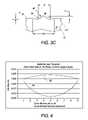
- FIG. 4experimental data on die bow for a thinned silicon die, or an interconnect, having no active circuitry, that has been laser processed with lasered features to form a laser textured component is illustrated.
- the bare semiconductor diewas a 3 mm ⁇ 10 mm silicon die singulated from a blank wafer that had been dry polished (i.e., thinned) to a thickness of about 100 ⁇ m.
- the semiconductor componentwas a 3 mm ⁇ 10 mm blank die from the same blank wafer but with the previously described laser processing step to form lasered features on the back side thereof substantially as previously described for laser features 48 ( FIG. 3C ).
- FIG. 3Cexperimental data on die bow for a thinned silicon die, or an interconnect, having no active circuitry, that has been laser processed with lasered features to form a laser textured component is illustrated.
- the bare semiconductor diewas a 3 mm ⁇ 10 mm silicon die singulated from a blank wafer that had been dry polished (i.e.,
- the vertical axis (y axis)represents Die Bow in (mm) for the die or the component.
- the horizontal axis (x axis)represents measured points ( 1 - 9 ) on the die or the component, with points 1 and 9 being proximate to the edges, and point 5 being proximate to the center.
- curve 66 in FIG. 4a thinned bare semiconductor die that has not been laser processed, bows in the shape of a smile (i.e., generally convex shape) with the center of the die deflected from the zero plane (0.000) by about ( ⁇ 0.019) mm.
- a thinned component having lasered featuresbows in the shape of a frown (i.e., generally concave shape) with the center of the component deflected from the zero plane by about (0.005) mm.
- the lasered features 48( FIG. 3C ) also provide an increased surface area for heat dissipation during operation of the semiconductor components 58 ( FIG. 1D ).
- the increased surface areafacilitates adhesion of the back sides 18 of the semiconductor components 58 ( FIG. 1D ) for packaging and other processes.
- the lasered features 48 ( FIG. 3C )also provide defect sites on the back sides 18 of the semiconductor components 58 ( FIG. 1D ) for trapping contaminants and improving the functionality of the semiconductor components 58 ( FIG. 1D ).
- the semiconductor components 58 ( FIG. 1D )can also include a separate gettering layer 102 ( FIG. 7E ) formed by laser processing.
- each pattern 70includes a plurality of elongated lasered features 72 in a generally parallel, spaced array. As shown in FIGS. 5B and 5C , each elongated lasered feature 72 includes an elongated ridge 74 and parallel spaced grooves 76 , 78 on either side of the ridge 74 .
- the elongated lasered features 72can be formed substantially as previously described for lasered feature 48 ( FIG. 3C ) but with the laser processing step configured to form the ridge 74 and the grooves 76 , 78 with a length (1) of from several microns to several centimeters or more.
- the process flowincludes the following sequence of steps.
- Step 90Provide a semiconductor wafer containing a plurality of semiconductor dice having a circuit side, a back side and integrated circuits and associated circuitry on the circuit side.
- Step 92Thin the wafer to a selected thickness.
- Step 92 Aadditional back side processing can be performed on the back side of the thinned wafer.
- the additional back side processescan include surface etching, such as chemical etching the entire back side, or selected areas thereof.
- Other back side processescan include surface cleaning, laser marking and screen printing of additional back side features.
- Other additional back side processescan include adding elements, such as dopants and fillers, to the back side of the thinned wafer.
- Step 94Laser process the back side of the thinned wafer to form one or more lasered features.
- Step 92 BOptionally, additional back side processing can be performed on the back side of the laser processed wafer, substantially as previously described for step 92 A.
- precut swatches of precured polymer filmas disclosed in U.S. Pat. No. 4,906,314, can be applied to the back side of the laser processed wafer.
- Step 96Dice the wafer into a plurality of components having the lasered features.
- the dicing stepcan be performed using a sawing process, a liquid jet process or a laser dicing process. With laser dicing the dicing step can be performed either prior to or after the laser processing step.
- FIGS. 7A-7Ea method for fabricating thinned semiconductor components 100 ( FIG. 7E ) using back side laser processing to form lasered features in the form of a gettering layer 102 ( FIG. 7E ) is illustrated.
- a semiconductor wafer 10 having a thickness of T 1 and containing a plurality of semiconductor dice 12can be provided, substantially as previously described.
- the wafer 10can be thinned on the carrier 24 from the back side 18 to form a thinned semiconductor wafer 10 T having a thickness of T 2 , substantially as previously described.
- a spin on dopant 98can be applied to the back side 18 of the thinned semiconductor wafer 10 T.
- Spin on dopantsare liquid solutions which can be used to form doped silicon like layers.
- the spin on dopantcan be applied to the back side 18 of the thinned semiconductor wafer 10 T by a spin coating process.
- the solutioncan be dispensed onto the wafer 10 T, which is then spun rapidly using a spin coater to evenly distribute the solution.
- the thickness of the resulting deposited materialdepends on the viscosity of the solution and the spin speed.
- Suitable dopantsinclude phosphorus, boron and arsenic.
- the dopant concentrationcan be varied by dilution with organic solvents (e.g., ethyl alcohol).
- the laser system 32can be used to drive the dopant in the spin on dopant 98 into the semiconductor substrate 14 .
- the drive in mechanismis diffusion caused by heating of the semiconductor substrate by the laser beams 44 to a required temperature, for a desired time period, for a desired effect.
- the heatingcan remain localized, such that the integrated circuits 23 ( FIG. 1E ), internal conductors 29 ( FIG. 1E ) and redistribution conductors 25 remain substantially unaffected.
- the thinned semiconductor wafer 10 Tcan be diced into a plurality of singulated semiconductor components 100 , substantially as previously described.
- Each semiconductor component 100includes a gettering layer 102 on the back side 18 thereof containing dopants driven into the semiconductor substrate 14 by the laser processing step.
- the dopants in the gettering layer 102provide defect sites on the back sides 18 of the semiconductor components 100 for attracting contaminants, and improving functionality.
- the semiconductor components 100can also include lasered features 48 ( FIG. 3C ) or 72 ( FIG. 5B ) formed as previously described concurrently with or separately from the gettering layer 102 .
- Interconnectscan be used to make electrical connections to semiconductor components.
- semiconductor test systemsinclude an interconnect for making temporary electrical connections to component contacts on the semiconductor components.
- the interconnectcan be chip sized or wafer sized.
- Interconnectsare also used to make permanent electrical connections to semiconductor components for various electronic assemblies, such as multi chip modules.
- Interconnectscan also include embedded semiconductor devices and integrated circuits.
- the interconnect 104includes an interconnect substrate 106 having a circuit side 110 and a back side 112 .
- the interconnect substrate 106can comprise a semiconductor material, substantially as previously described for the semiconductor substrate 14 ( FIG. 1A ). However, in this case the interconnect substrate 106 do not necessarily include integrated circuits, which can be embedded separately using a separate circuit substrate 114 .
- the interconnect substrate 106includes a plurality of interconnect contacts 108 A, 108 B, 108 C on the circuit side 110 configured to make electrical connections with semiconductor components (or alternately to the circuit substrate 114 ). For illustrative purposes, three types of interconnect contacts 108 A, 108 B, 108 C are illustrated. However, in actual practice the interconnect substrate 106 may only include one type of interconnect contact 108 A, 108 B, or 108 C.
- the interconnect contact 108 Acan comprise a metallized pillar configured to contact a flat planar component contact such as a bond pad or redistribution pad.
- the interconnect contact 108 Bcan comprise a metallized pillar configured to penetrate a raised component contact such as a metal bump or ball.
- the interconnect contact 108 Ccan comprise a metallized recess configured to contact a raised component contact such as a metal bump or ball.
- the interconnect contact 108 Ccan be configured to physically and electrically contact the circuit substrate 114 .
- U.S. Pat. No. 7,129,156 B2which is incorporated herein by reference, further describes the interconnect contacts 108 A, 108 B and 108 C, and suitable methods of fabrication.
- U.S. Pat. No. 7,498,675 B2which is incorporated herein by reference, further describes components having conductive vias, and additional circuit elements, such as back side redistribution layers, in electrical communication with the conductive vias.
- the interconnect contact 108 Ccan also include a conductive via 116 through the interconnect substrate 106 configured to make back side electrical connections to the interconnect contact 108 C and the circuit substrate 114 .
- the via 116can be placed in electrical communication with electrodes on a module substrate or test fixture.
- the interconnect contacts 108 A and 108 Bcan also include conductive vias configured to make back side electrical connections.
- the circuit substrate 114can comprise a thinned semiconductor die, or portion thereof, configured to fit in the interconnect contact 108 C in electrical communication with the conductive via 116 .
- the back side 112 of the interconnect substrate 106can be thinned and then laser processed with lasered features substantially as previously described for the thinned wafer 10 T ( FIG. 1C ).
- the lasered featurescan be used to rigidify the interconnect 108 and to increase the surface area of the back side 112 , substantially as previously described. Further, the laser processing of the back side 112 can be performed to not affect the interconnect contacts 108 A, 108 B, 108 C on the circuit side 110 .
Landscapes
- Engineering & Computer Science (AREA)
- Physics & Mathematics (AREA)
- Condensed Matter Physics & Semiconductors (AREA)
- Power Engineering (AREA)
- Microelectronics & Electronic Packaging (AREA)
- Computer Hardware Design (AREA)
- General Physics & Mathematics (AREA)
- Manufacturing & Machinery (AREA)
- High Energy & Nuclear Physics (AREA)
- Toxicology (AREA)
- Health & Medical Sciences (AREA)
- Optics & Photonics (AREA)
- Electromagnetism (AREA)
- Dicing (AREA)
- Laser Beam Processing (AREA)
Abstract
Description
- Semiconductor components, such as dice, packages and interconnects are being made thinner than previous generation components. At the same time, electrical and packaging requirements for semiconductor components are becoming more stringent. Typically, semiconductor components are thinned from the back side at the wafer level using a process such as grinding or chemical mechanical planarization (CMP). For example, a standard 200 mm (8 inch) diameter semiconductor wafer has a thickness of about 725 μm. During fabrication, the wafer can be thinned to a thickness of about 100 μm or less.
- Back side thinning of a semiconductor wafer can cause problems during wafer level processes, during component fabrication processes, and in the singulated components as well. One problem is that the thinned wafer can bow due to stresses generated by the circuitry formed on the circuit side (face) of the wafer. In this case, a thinned wafer oriented circuit side up can bow upward in the shape of a smile (i.e., generally convex shape), causing carrier adhesion, wafer handling and alignment issues during component fabrication. A singulated component from a thinned wafer can also bow upward towards the circuit side, and from the corners towards the center of the component. Bowed components can be more difficult to mount, particularly in flip chip and stacking applications. For example, terminal contacts on a bowed flip chip or stacked component can pull away from mating electrodes or contacts on a substrate or adjacent component.
- Another problem caused by thinning is that the back side of a thinned semiconductor component can have a smooth, polished surface, reducing the number of defect sites. The defect sites can trap contaminants in the semiconductor substrate and can also act as carrier generation and recombination centers. The contaminants can adversely affect the minority carrier lifetime electrons of the semiconductor devices changing functionality and certain defect mechanisms. One technique for attracting contaminants is to deposit a gettering agent, such as a spin-on dopant, on the back side of a component. However, relatively high temperatures (e.g., >800° C.) are required to drive the dopant into the semiconductor substrate. A thinned semiconductor component typically includes circuitry on the circuit side, which cannot be subjected to high temperatures. For this reason, thinned semiconductor components do not usually employ an extrinsic back side gettering layer due to the difficulties in applying this layer. In addition, thinned semiconductor components can have different electrical characteristics and a different functionality than full thickness components.
- In view of the foregoing, improved thinned semiconductor components, and improved methods for fabricating thinned semiconductor components are needed in the art. However, the foregoing examples of the related art and limitations related therewith, are intended to be illustrative and not exclusive. Other limitations of the related art will become apparent to those of skill in the art upon a reading of the specification and a study of the drawings.
- Exemplary embodiments are illustrated in the referenced figures of the drawings. It is intended that the embodiments and the figures disclosed herein are to be considered illustrative rather than limiting.
FIGS. 1A-1D are schematic cross sectional views illustrating steps in a method for fabricating thinned semiconductor components using back side laser processing to form lasered features;FIG. 1E is an enlarged schematic cross sectional view taken alongline 1E-1E ofFIG. 2A illustrating integrated circuits and associated circuitry on a semiconductor wafer;FIG. 1F is an enlarged schematic cross sectional view taken alongline 1F ofFIG. 1C illustrating a laser processing step;FIG. 2A is a schematic view taken alongline 2A-2A ofFIG. 1A illustrating a circuit side of the semiconductor wafer;FIG. 2B is a schematic view taken alongline 2B-2B ofFIG. 1B illustrating a back side of the semiconductor wafer;FIG. 2C is a schematic view taken alongline 2C-2C ofFIG. 1D illustrating the back side of the semiconductor wafer following the laser processing step;FIG. 3A is an enlarged schematic view taken along line3A ofFIG. 2B illustrating the back side of the semiconductor wafer following a thinning step;FIG. 3B is an enlarged schematic view taken alongline 3B ofFIG. 2C illustrating the back side of the semiconductor wafer following the laser processing step;FIG. 3C is an enlarged schematic cross sectional view taken along line3C-3C ofFIG. 3B illustrating a lasered feature on the back side of the semiconductor wafer following the laser processing step;FIG. 4 is a graph illustrating die bow in mm for nine points for a bare silicon die and for a component having a pattern of laser textured features on the back side;FIG. 5A is a schematic bottom view of a singulated semiconductor component illustrating patterns of lasered features in the corners configured to rigidify and reduce bowing of the corners;FIG. 5B is an enlarged schematic cross sectional view taken alongline 5B-5B ofFIG. 5A illustrating a lasered feature;FIG. 5C is an enlarged schematic plan view taken along line5C-5C ofFIG. 5B illustrating the lasered feature;FIG. 6 is a process flow chart of the method;FIGS. 7A-7E are schematic cross sectional views illustrating steps in a method for fabricating thinned semiconductor components using back side laser processing to form a gettering layer; andFIG. 8 is a schematic cross sectional view of a thinned semiconductor interconnect fabricated using back side laser processing.- As used herein, “semiconductor component” means an electronic element that includes a semiconductor substrate having integrated circuits and semiconductor devices. “Interconnect” means an electrical element that makes electrical contact with a semiconductor component or an embedded circuitry. “Wafer-level” means a process conducted on an element, such as a semiconductor wafer, containing multiple semiconductor components. “Wafer size” means having an outline about the same as that of a semiconductor wafer. “Die level” means a process conducted on a singulated semiconductor component. “Chip scale” means a semiconductor component having an outline about the same as that of a semiconductor die.
- Referring to
FIGS. 1A-1D , steps in a method for fabricating thinned semiconductor components58 (FIG. 1D ) using back side laser processing are illustrated. Initially, as shown inFIGS. 1A and 2A , asemiconductor wafer 10 containing a plurality ofsemiconductor dice 12 can be provided. Although in the illustrative embodiment, the method is performed on anentire semiconductor wafer 10, it is to be understood that the method can be performed on a portion of asemiconductor wafer 10, on a panel, or on any other substrate that contains semiconductor dice or components. As another alternative, for fabricating interconnects the method can be performed on a blank semiconductor wafer containing no active semiconductor dice. - The
semiconductor wafer 10 can comprise a conventional semiconductor wafer having a standard diameter and a full thickness (T1). By way of example, a 150 mm diameter wafer has a full thickness (T1) of about 675 μm, a 200 mm diameter wafer has a full thickness (T1) of about 725 μm, and a 300 mm diameter wafer has a full thickness (T1) of about 775 μm. In the illustrative embodiment, thesemiconductor wafer 10 comprises silicon (Si). However, thesemiconductor wafer 10 can comprise another material such GaAs, SiC or sapphire. - The
dice 12 can comprise conventional semiconductor dice having a desired configuration, and formed using conventional semiconductor fabrication processes. For example, each die12 can comprise a dynamic random access memory (DRAM), a static random access memory (SRAM), a flash memory, a microprocessor, a digital signal processor (DSP) or an application specific integrated circuit (ASIC). In addition, each die12 can have any polygonal shape. In the illustrative embodiment, thedice 12 are generally square in shape, but other polygonal shapes, such as rectangular or hexagonal can also be utilized. Using laser dicing in combination with the method a wider range of shapes for each die12 can be effected (e.g., triangular, oval, circular). - As shown in
FIG. 1A , thewafer 10 and each die12 includes asemiconductor substrate 14 having a circuit side16 (first side) wherein integrated circuits23 (FIG. 1E ) and associated circuitry are located, and a back side18 (second side). Thecircuit side 16 and theback side 18 are the major planar surfaces of thewafer 10 and thedice 12. In addition, thedice 12 are separated by streets20 (FIG. 2A ) formed on thecircuit side 16 of thewafer 10. Further, as shown inFIG. 2A , each die12 includes a pattern ofdie contacts 22 formed on thecircuit side 16 in a selected pattern, such as a dense area array, in electrical communication with integrated circuits23 (FIG. 1E ) in thesemiconductor substrate 14. As shown inFIG. 1E , each die12 can includeredistribution conductors 25,device bond pads 27, andinternal conductors 29, configured to establish electrical communication between thedie contacts 22 and theintegrated circuits 23. As also shown inFIG. 1E , each die12 can include aninner dielectric layer 31, and anouter dielectric layer 33 which electrically insulates theredistribution conductors 25. All of these elements are conventional in the art, and can be formed using conventional semiconductor fabrication processes. - Next, as shown in
FIG. 1B , a thinning step can be performed on theback side 18 of thewafer 10 to form a thinnedsemiconductor wafer 10T. For performing the thinning step, thewafer 10 can also be attached to acarrier 24, such as a conventional glass or silicon carrier. Thewafer 10 can be attached to thecarrier 24 with thecircuit side 16 bonded to thecarrier 24, and with theback side 18 exposed for thinning. Thewafer 10 can be attached to thecarrier 24 using acarrier adhesive 26, such as a double sided tape, or a spin coat adhesive, which can be de-bonded using UV radiation for a glass carrier, or thermal radiation for a silicon carrier. However, the carrier is optional as thewafer 10 can be thinned without using a carrier. - The thinning step can be performed using a mechanical planarization process, such as dry polishing, performed with a
mechanical planarization apparatus 28. Suitable mechanical planarization apparatus are manufactured by Accretec of Bloomfield, Mich., and Disco Corporation of Santa Clara, Calif. The thinning step can also be performed using a chemical mechanical planarization (CMP) apparatus, or using an etch back process, such as a wet etch process, a dry etch process or a plasma etching process, either performed alone or in combination with mechanical planarization. The thickness T2 of the thinnedwafer 10T can be selected as desired with from 35 μm to 150 μm being representative, and less than 100 μm being preferred. Theback side 18 of the thinnedwafer 10T has a smooth, polished surface, and is devoid of features. The thinnedwafer 10T can be susceptible to bowing particularly if other features, such as circuit side and back side redistribution (RDL) layers, are added. - Next, as shown in
FIG. 1C , a laser processing step is performed on thebackside 18 of the thinnedwafer 10T using alaser system 32. As shown inFIG. 1F , the laser processing step can be used to form a textured surface comprised of lasered features48 on thebackside 18 of the thinnedwafer 10T. As will be further explained, the laser processing step can also be performed to form different types of lasered features, configured to accomplish a variety of structural and functional changes on the thinnedwafer 10T anddice 12, particularly on areas of theback side 18 of the thinnedwafer 10T. For example, laser processing can be used to form lasered features which incorporate materials such as dopants and fillers into selected areas on the entire theback side 18 of the thinnedwafer 10T. In this case, the lasered features may not be visible geometrical features, but the physical or electrical characteristics of the silicon has been changed to accomplish a desired purpose (e.g., carrier modification, gettering properties, mechanical properties, visual properties). As another example, the laser processing step can be performed to melt and re-solidified the silicon into re-cast lasered features having a different crystal lattice structure (e.g., amorphous silicon to polysilicon). Again the lasered features formed by the re-solidified material can have desired physical or electrical characteristics relative to material that has not been laser processed. - The laser processing step can be performed using a variety of conventional laser systems used in the art. In the illustrative embodiment, the
laser system 32 includes alaser source 34 configured to produce alaser beam 42, anexpander 36 configured to expand thelaser beam 42, alens system 50 configured to redirect the expandedlaser beam 42 by ninety degrees, a DOE (diffractive optical element)38 configured to separate thelaser beam 42 into a plurality ofseparate laser beams 44, and a focusingdevice 40 configured to focus thelaser beams 44 onto theback side 18 of the thinnedwafer 10T. Thelaser system 32 can also include awafer handler 46 configured to align and move the thinnedwafer 10T past the laser beams44. Onesuitable laser system 32 is commercially available from ALSI (Advanced Laser Separation International) located at Platinawerf 20-G, Beunigen 6641 TL, Netherlands. Thislaser system 32 is designed to dice semiconductor wafers but can be adapted to perform the present laser processing step. The operational parameters of thelaser system 32 can be selected as required depending on the application. - As shown in
FIG. 2C , the thinnedsemiconductor wafer 10T can be moved past the focusing device40 (FIG. 1C ) such that the lasered features48 (FIG. 1F ) are formed along parallel, spacedscan lines 52. Each lasered feature48 (FIG. 1F ) can be formed using from one to several laser pulses directed at the same location. Thehorizontal scan lines 52 are generally parallel to thehorizontal edges 60 of thedice 12, and generally orthogonal to thevertical edges 62 of thedice 12. As the lasered features48 (FIG. 1F ) have micron sized dimensions, they are not visible to the naked eye, or in the scale ofFIG. 2C . On the other hand,FIG. 3B has a scale of about 100× actual size, such that the lasered features48, and their orientation along thescan lines 52 relative to the edges of thesemiconductor dice 12, are visible. InFIG. 3C , the cross sectional shape of the lasered features48 is visible. - As shown in
FIG. 3B , the lasered features48 can be formed on the entireback side 18 of the thinnedsemiconductor wafer 10T, or within the footprint of each individual semiconductor die12, and in a repetitive straight line pattern equally spaced along the scan lines52. However, the location and the pattern of the lasered features48 can be selected for particular applications. For example, the lasered features48 can be formed on only selected portions of thesemiconductor wafer 10T and dice12 (e.g., along the edges, in the corners, in the middle, away from active devices or circuitry, in the streets). The lasered features48 can also be formed in different patterns than the straight line pattern ofFIG. 3B (e.g., along curves). In addition, a plurality of the lasered features48 can be located in particular areas of thesemiconductor wafer 10T anddice 12 to form selected geometrical shapes (e.g., circles, squares, triangles or any geometrical shape). - As shown in
FIG. 3C , each laseredfeature 48 can include a shallow, donut-shapedgroove 54, which extends into theback side 18 of the thinnedwafer 10T with a depth (d). Each lasered feature48 (FIG. 3C ) can also include a bump56 (or elevated feature) surrounded by thegroove 54, which has a height (h) relative to theback side 18 of the thinnedwafer 10T. In the illustrative embodiment, thebump 56 is elevated and shaped like a bell or a hillock, but other shapes are possible (e.g., elevated, conical, pyramidal, spherical). Also in the illustrative embodiment, each laseredfeature 48 can have a selected pitch (P) and an outside diameter (OD) of about 4-8 μm. Thegroove 54 can have a depth (d) of about 0.25 to 1.0 μm, thebump 56 can have a base diameter (D) of about 4-6 μm, and thebump 56 can have a height (h) of about 1-2 μm. However, these dimensions are exemplary, and the lasered features48 can be formed with other dimensions and shapes as well. - It is theorized that the
bumps 56 of the lasered features48 (FIG. 3C ) are formed by molten material, which is produced by localized heating of thesemiconductor substrate 14 by energy from thelaser beam 44, collecting and re-solidifying with an elevated topography. Depending on the conditions, the re-solidified material can comprise polysilicon or amorphous silicon. It is theorized that thegrooves 54 are formed by the attraction of molten material from thesemiconductor substrate 14 into thebumps 56. - For some applications one or more additional elements can also be incorporated into the
bumps 56 or onto other selected areas of theback side 18 of the thinnedwafer 10T. For example, during laser processing one or more additional elements, such as dopants and fillers, in solid, gas or liquid form can be incorporated into the liquid or semi-liquid phase silicon. Upon re-solidification, the incorporated element can perform a desired function, such as carrier modification, visual contrast or strengthening for different applications such as laser marking. Also, during (or following) laser processing it may be necessary to balance the inherent circuit side stresses on thewafer 10T anddice 12 with the newly formed back side stresses, to achieve flatness, uniformity and planarity in thewafer 10T anddice 12. For example, stress balancing can be achieved using fillers, or structures, on thecircuit side 16 and theback side 18 of thewafer 10T, or only on selected areas thereof (e.g., proximate to the edges). - Referring to
FIG. 1D , following the laser processing step (FIG. 1C ), the thinnedsemiconductor wafer 10T can be diced along dicinglines 84 to form a plurality of chipscale semiconductor components 58. Dicing can be accomplished using a process such as lasering, sawing, water jetting or etching. Following the dicing step, thesemiconductor components 58 can be removed from thecarrier 24. Eachsingulated semiconductor component 58 has a footprint corresponding to a semiconductor die12 (FIG. 2A ) and includes a pattern of lasered features48 (FIG. 3C ) on theback side 18 thereof. - The lasered features48 (
FIG. 3C ) help to counteract bowing in the thinnedsemiconductor wafer 10T, and insingulated semiconductor components 58. In particular, a thinned semiconductor wafer that has not been laser processed, and the singulated semiconductor components from the wafer, may bow upward in the shape of a smile (i.e., generally convex shape). On the other hand, the thinnedsemiconductor wafer 10T having lasered features48 (FIG. 3C ), and the singulated semiconductor components58 (FIG. 1D ) from thewafer 10T may bow by a lesser amount, with the bow direction being downward in the shape of a frown (i.e., generally concave shape). Bowing can also be counteracted by balancing the front side stresses with the back side stresses. - Referring to
FIG. 4 , experimental data on die bow for a thinned silicon die, or an interconnect, having no active circuitry, that has been laser processed with lasered features to form a laser textured component is illustrated. The bare semiconductor die was a 3 mm×10 mm silicon die singulated from a blank wafer that had been dry polished (i.e., thinned) to a thickness of about 100 μm. The semiconductor component was a 3 mm×10 mm blank die from the same blank wafer but with the previously described laser processing step to form lasered features on the back side thereof substantially as previously described for laser features48 (FIG. 3C ). InFIG. 4 , the vertical axis (y axis) represents Die Bow in (mm) for the die or the component. The horizontal axis (x axis) represents measured points (1-9) on the die or the component, withpoints point 5 being proximate to the center. As represented bycurve 66 inFIG. 4 , a thinned bare semiconductor die that has not been laser processed, bows in the shape of a smile (i.e., generally convex shape) with the center of the die deflected from the zero plane (0.000) by about (−0.019) mm. As represented bycurve 64 inFIG. 4 , a thinned component having lasered features bows in the shape of a frown (i.e., generally concave shape) with the center of the component deflected from the zero plane by about (0.005) mm. - In addition to counteracting bowing in the thinned
semiconductor wafer 10T, and in the semiconductor components58 (FIG. 1D ), the lasered features48 (FIG. 3C ) also provide an increased surface area for heat dissipation during operation of the semiconductor components58 (FIG. 1D ). In addition, the increased surface area facilitates adhesion of the back sides18 of the semiconductor components58 (FIG. 1D ) for packaging and other processes. The lasered features48 (FIG. 3C ) also provide defect sites on the back sides18 of the semiconductor components58 (FIG. 1D ) for trapping contaminants and improving the functionality of the semiconductor components58 (FIG. 1D ). As will be further explained, the semiconductor components58 (FIG. 1D ) can also include a separate gettering layer102 (FIG. 7E ) formed by laser processing. - Referring to
FIGS. 5A-5C , asemiconductor component 68 having patterns70 (FIG. 5A ) of elongated lasertextured features 72 on a back side80 (FIG. 5A ) thereof is illustrated. The elongated laser features72 are located proximate to the corners82 (FIG. 5A ) of thecomponent 68, and function to rigidify and prevent flexure of thecorners 82. Eachpattern 70 includes a plurality of elongated lasered features72 in a generally parallel, spaced array. As shown inFIGS. 5B and 5C , each elongated laseredfeature 72 includes anelongated ridge 74 and parallel spacedgrooves ridge 74. The elongated lasered features72 can be formed substantially as previously described for lasered feature48 (FIG. 3C ) but with the laser processing step configured to form theridge 74 and thegrooves - Referring to
FIG. 6 , the previously described method is illustrated in a process flow chart. The process flow includes the following sequence of steps. Step 90—Provide a semiconductor wafer containing a plurality of semiconductor dice having a circuit side, a back side and integrated circuits and associated circuitry on the circuit side.Step 92—Thin the wafer to a selected thickness.Step 92A—Optionally, additional back side processing can be performed on the back side of the thinned wafer. The additional back side processes can include surface etching, such as chemical etching the entire back side, or selected areas thereof. Other back side processes can include surface cleaning, laser marking and screen printing of additional back side features. Other additional back side processes can include adding elements, such as dopants and fillers, to the back side of the thinned wafer.Step 94—Laser process the back side of the thinned wafer to form one or more lasered features.Step 92B—Optionally, additional back side processing can be performed on the back side of the laser processed wafer, substantially as previously described forstep 92A. As another optional step, precut swatches of precured polymer film, as disclosed in U.S. Pat. No. 4,906,314, can be applied to the back side of the laser processed wafer.Step 96—Dice the wafer into a plurality of components having the lasered features. The dicing step can be performed using a sawing process, a liquid jet process or a laser dicing process. With laser dicing the dicing step can be performed either prior to or after the laser processing step.- Referring to
FIGS. 7A-7E , a method for fabricating thinned semiconductor components100 (FIG. 7E ) using back side laser processing to form lasered features in the form of a gettering layer102 (FIG. 7E ) is illustrated. Initially, as shown inFIG. 7A , asemiconductor wafer 10 having a thickness of T1 and containing a plurality ofsemiconductor dice 12 can be provided, substantially as previously described. In addition, as shown inFIG. 7B , thewafer 10 can be thinned on thecarrier 24 from theback side 18 to form a thinnedsemiconductor wafer 10T having a thickness of T2, substantially as previously described. - Next, as shown in
FIG. 7C , a spin ondopant 98 can be applied to theback side 18 of the thinnedsemiconductor wafer 10T. Spin on dopants are liquid solutions which can be used to form doped silicon like layers. The spin on dopant can be applied to theback side 18 of the thinnedsemiconductor wafer 10T by a spin coating process. For performing the spin coating process the solution can be dispensed onto thewafer 10T, which is then spun rapidly using a spin coater to evenly distribute the solution. The thickness of the resulting deposited material depends on the viscosity of the solution and the spin speed. Suitable dopants include phosphorus, boron and arsenic. The dopant concentration can be varied by dilution with organic solvents (e.g., ethyl alcohol). - Next, as shown in
FIG. 7D , thelaser system 32 can be used to drive the dopant in the spin ondopant 98 into thesemiconductor substrate 14. In this case, the drive in mechanism is diffusion caused by heating of the semiconductor substrate by thelaser beams 44 to a required temperature, for a desired time period, for a desired effect. However, the heating can remain localized, such that the integrated circuits23 (FIG. 1E ), internal conductors29 (FIG. 1E ) andredistribution conductors 25 remain substantially unaffected. - Next, as shown in
FIG. 7E , the thinnedsemiconductor wafer 10T can be diced into a plurality ofsingulated semiconductor components 100, substantially as previously described. Eachsemiconductor component 100 includes agettering layer 102 on theback side 18 thereof containing dopants driven into thesemiconductor substrate 14 by the laser processing step. The dopants in thegettering layer 102 provide defect sites on the back sides18 of thesemiconductor components 100 for attracting contaminants, and improving functionality. In addition to thegettering layer 102, thesemiconductor components 100 can also include lasered features48 (FIG. 3C ) or72 (FIG. 5B ) formed as previously described concurrently with or separately from thegettering layer 102. - Referring to
FIG. 8 , the previously described method can also be used to fabricate a thinnedinterconnect 104. Interconnects can be used to make electrical connections to semiconductor components. For example, semiconductor test systems include an interconnect for making temporary electrical connections to component contacts on the semiconductor components. Depending on the system, the interconnect can be chip sized or wafer sized. Interconnects are also used to make permanent electrical connections to semiconductor components for various electronic assemblies, such as multi chip modules. Interconnects can also include embedded semiconductor devices and integrated circuits. - As shown in
FIG. 8 , theinterconnect 104 includes aninterconnect substrate 106 having acircuit side 110 and aback side 112. Theinterconnect substrate 106 can comprise a semiconductor material, substantially as previously described for the semiconductor substrate14 (FIG. 1A ). However, in this case theinterconnect substrate 106 do not necessarily include integrated circuits, which can be embedded separately using aseparate circuit substrate 114. Theinterconnect substrate 106 includes a plurality ofinterconnect contacts circuit side 110 configured to make electrical connections with semiconductor components (or alternately to the circuit substrate114). For illustrative purposes, three types ofinterconnect contacts interconnect substrate 106 may only include one type ofinterconnect contact - As shown in
FIG. 8 , theinterconnect contact 108A can comprise a metallized pillar configured to contact a flat planar component contact such as a bond pad or redistribution pad. Theinterconnect contact 108B can comprise a metallized pillar configured to penetrate a raised component contact such as a metal bump or ball. Theinterconnect contact 108C can comprise a metallized recess configured to contact a raised component contact such as a metal bump or ball. Alternately, theinterconnect contact 108C can be configured to physically and electrically contact thecircuit substrate 114. U.S. Pat. No. 7,129,156 B2, which is incorporated herein by reference, further describes theinterconnect contacts - As shown in
FIG. 8 , theinterconnect contact 108C can also include a conductive via116 through theinterconnect substrate 106 configured to make back side electrical connections to theinterconnect contact 108C and thecircuit substrate 114. For example, the via116 can be placed in electrical communication with electrodes on a module substrate or test fixture. Theinterconnect contacts circuit substrate 114 can comprise a thinned semiconductor die, or portion thereof, configured to fit in theinterconnect contact 108C in electrical communication with the conductive via116. - The
back side 112 of theinterconnect substrate 106 can be thinned and then laser processed with lasered features substantially as previously described for the thinnedwafer 10T (FIG. 1C ). The lasered features can be used to rigidify the interconnect108 and to increase the surface area of theback side 112, substantially as previously described. Further, the laser processing of theback side 112 can be performed to not affect theinterconnect contacts circuit side 110. - While a number of exemplary aspects and embodiments have been discussed above, those of skill in the art will recognize certain modifications, permutations, additions and sub-combinations thereof. It is therefore intended that the following appended claims and claims hereafter introduced are interpreted to include all such modifications, permutations, additions and sub-combinations as are within their true spirit and scope.
Claims (42)
Priority Applications (3)
| Application Number | Priority Date | Filing Date | Title |
|---|---|---|---|
| US12/424,726US8187983B2 (en) | 2009-04-16 | 2009-04-16 | Methods for fabricating semiconductor components using thinning and back side laser processing |
| US13/473,644US8530895B2 (en) | 2009-04-16 | 2012-05-17 | Thinned semiconductor components having lasered features and method of fabrication |
| US13/960,855US8728921B2 (en) | 2009-04-16 | 2013-08-07 | Method for fabricating semiconductor components having lasered features containing dopants |
Applications Claiming Priority (1)
| Application Number | Priority Date | Filing Date | Title |
|---|---|---|---|
| US12/424,726US8187983B2 (en) | 2009-04-16 | 2009-04-16 | Methods for fabricating semiconductor components using thinning and back side laser processing |
Related Child Applications (1)
| Application Number | Title | Priority Date | Filing Date |
|---|---|---|---|
| US13/473,644DivisionUS8530895B2 (en) | 2009-04-16 | 2012-05-17 | Thinned semiconductor components having lasered features and method of fabrication |
Publications (2)
| Publication Number | Publication Date |
|---|---|
| US20100264423A1true US20100264423A1 (en) | 2010-10-21 |
| US8187983B2 US8187983B2 (en) | 2012-05-29 |
Family
ID=42980336
Family Applications (3)
| Application Number | Title | Priority Date | Filing Date |
|---|---|---|---|
| US12/424,726Active2030-05-06US8187983B2 (en) | 2009-04-16 | 2009-04-16 | Methods for fabricating semiconductor components using thinning and back side laser processing |
| US13/473,644ActiveUS8530895B2 (en) | 2009-04-16 | 2012-05-17 | Thinned semiconductor components having lasered features and method of fabrication |
| US13/960,855ActiveUS8728921B2 (en) | 2009-04-16 | 2013-08-07 | Method for fabricating semiconductor components having lasered features containing dopants |
Family Applications After (2)
| Application Number | Title | Priority Date | Filing Date |
|---|---|---|---|
| US13/473,644ActiveUS8530895B2 (en) | 2009-04-16 | 2012-05-17 | Thinned semiconductor components having lasered features and method of fabrication |
| US13/960,855ActiveUS8728921B2 (en) | 2009-04-16 | 2013-08-07 | Method for fabricating semiconductor components having lasered features containing dopants |
Country Status (1)
| Country | Link |
|---|---|
| US (3) | US8187983B2 (en) |
Cited By (17)
| Publication number | Priority date | Publication date | Assignee | Title |
|---|---|---|---|---|
| WO2013036436A1 (en)* | 2011-09-07 | 2013-03-14 | Qualcomm Mems Technologies, Inc. | Mechanical layer for interferometric modulators and methods of making the same |
| US8669166B1 (en)* | 2012-08-15 | 2014-03-11 | Globalfoundries Inc. | Methods of thinning and/or dicing semiconducting substrates having integrated circuit products formed thereon |
| US20140080289A1 (en)* | 2012-09-20 | 2014-03-20 | Disco Corporation | Method of forming gettering layer |
| CN103831529A (en)* | 2012-11-20 | 2014-06-04 | 三星显示有限公司 | Laser processing apparatus |
| WO2014209593A1 (en)* | 2013-06-24 | 2014-12-31 | Qualcomm Incorporated | Stress compensation patterning |
| US8964280B2 (en) | 2006-06-30 | 2015-02-24 | Qualcomm Mems Technologies, Inc. | Method of manufacturing MEMS devices providing air gap control |
| US20160163611A1 (en)* | 2014-12-03 | 2016-06-09 | International Business Machines Corporation | Laminate substrates having radial cut metallic planes |
| US9636783B2 (en) | 2014-04-30 | 2017-05-02 | International Business Machines Corporation | Method and apparatus for laser dicing of wafers |
| CN108140556A (en)* | 2015-08-22 | 2018-06-08 | 东京毅力科创株式会社 | Substrate Backside Texturing |
| WO2023028729A1 (en)* | 2021-08-30 | 2023-03-09 | Yangtze Memory Technologies Co., Ltd. | Wafer stress control and semiconductor structure |
| US11929119B2 (en) | 2021-06-30 | 2024-03-12 | Yangtze Memory Technologies Co., Ltd. | Three-dimensional memory devices and memory system |
| US11996152B2 (en) | 2021-06-30 | 2024-05-28 | Yangtze Memory Technologies Co., Ltd. | Three-dimensional memory devices and methods for forming the same |
| US12020750B2 (en) | 2021-06-30 | 2024-06-25 | Yangtze Memory Technologies Co., Ltd. | Three-dimensional memory devices |
| US12069854B2 (en) | 2021-06-30 | 2024-08-20 | Yangtze Memory Technologies Co., Ltd. | Three-dimensional memory devices and methods for forming the same |
| US12113037B2 (en) | 2021-06-30 | 2024-10-08 | Yangtze Memory Technologies Co., Ltd. | Three-dimensional memory devices and methods for forming the same |
| US12170257B2 (en) | 2021-06-30 | 2024-12-17 | Yangtze Memory Technologies Co., Ltd. | Three-dimensional memory devices and methods for forming the same |
| US12388036B2 (en) | 2021-06-30 | 2025-08-12 | Yangtze Memory Technologies Co., Ltd. | Three-dimensional memory devices and methods for forming the same |
Families Citing this family (5)
| Publication number | Priority date | Publication date | Assignee | Title |
|---|---|---|---|---|
| US8187983B2 (en) | 2009-04-16 | 2012-05-29 | Micron Technology, Inc. | Methods for fabricating semiconductor components using thinning and back side laser processing |
| US20150044783A1 (en)* | 2013-08-12 | 2015-02-12 | Micron Technology, Inc. | Methods of alleviating adverse stress effects on a wafer, and methods of forming a semiconductor device |
| JP6341279B2 (en)* | 2014-07-03 | 2018-06-13 | 新日鐵住金株式会社 | Laser processing equipment |
| DE102018006806B4 (en)* | 2018-08-26 | 2023-01-19 | Hochschule Mittweida (Fh) | Use of at least one laser for structuring at least one area of a surface of a substrate with at least one microelectronic component and/or as a carrier for microelectronic units |
| US11817304B2 (en)* | 2019-12-30 | 2023-11-14 | Micron Technology, Inc. | Method of manufacturing microelectronic devices, related devices, systems, and apparatus |
Citations (63)
| Publication number | Priority date | Publication date | Assignee | Title |
|---|---|---|---|---|
| US4668304A (en)* | 1985-04-10 | 1987-05-26 | Eaton Corporation | Dopant gettering semiconductor processing by excimer laser |
| US4906314A (en)* | 1988-12-30 | 1990-03-06 | Micron Technology, Inc. | Process for simultaneously applying precut swatches of precured polyimide film to each semiconductor die on a wafer |
| US5322988A (en)* | 1990-03-29 | 1994-06-21 | The United States Of America As Represented By The Secretary Of The Navy | Laser texturing |
| US5922224A (en)* | 1996-02-09 | 1999-07-13 | U.S. Philips Corporation | Laser separation of semiconductor elements formed in a wafer of semiconductor material |
| US6107109A (en)* | 1997-12-18 | 2000-08-22 | Micron Technology, Inc. | Method for fabricating a semiconductor interconnect with laser machined electrical paths through substrate |
| US6509546B1 (en)* | 2000-03-15 | 2003-01-21 | International Business Machines Corporation | Laser excision of laminate chip carriers |
| US20030052102A1 (en)* | 2001-09-11 | 2003-03-20 | Seiko Epson Corporation | Laser processing method and laser processing apparatus |
| US6638358B1 (en)* | 2000-01-13 | 2003-10-28 | Advanced Micro Devices, Inc. | Method and system for processing a semiconductor device |
| US6676878B2 (en)* | 2001-01-31 | 2004-01-13 | Electro Scientific Industries, Inc. | Laser segmented cutting |
| US20040013149A1 (en)* | 2002-07-17 | 2004-01-22 | Sharp Kabushiki Kaisha | Nitride semiconductor laser device chip and laser apparatus including the same |
| US20040046288A1 (en)* | 2000-07-18 | 2004-03-11 | Chou Stephen Y. | Laset assisted direct imprint lithography |
| US6734387B2 (en)* | 1999-05-27 | 2004-05-11 | Spectra Physics Lasers, Inc. | Method and apparatus for micro-machining of articles that include polymeric materials |
| US6734032B2 (en)* | 2000-08-25 | 2004-05-11 | Micron Technology, Inc. | Method and apparatus for marking a bare semiconductor die |
| US6737606B2 (en)* | 2001-09-10 | 2004-05-18 | Micron Technology, Inc. | Wafer dicing device and method |
| US20040124184A1 (en)* | 2002-06-11 | 2004-07-01 | Chengwu An | Method and apparatus for forming periodic structures |
| US20050151138A1 (en)* | 2003-11-12 | 2005-07-14 | Slater David B.Jr. | Methods of processing semiconductor wafer backsides having light emitting devices (LEDS) thereon and leds so formed |
| US6924210B1 (en)* | 2004-03-06 | 2005-08-02 | International Business Machines Corporation | Chip dicing |
| US6927167B2 (en)* | 2002-12-11 | 2005-08-09 | Denso Corporation | Method for manufacturing semiconductor device having controlled surface roughness |
| US20050227379A1 (en)* | 2004-04-01 | 2005-10-13 | Matthew Donofrio | Laser patterning of light emitting devices and patterned light emitting devices |
| US20060076649A1 (en)* | 2003-05-30 | 2006-04-13 | S.O.I. Tec Silicon On Insulator Technologies S.A. | Substrate for stressed systems and method of making same |
| US7041578B2 (en)* | 2003-07-02 | 2006-05-09 | Texas Instruments Incorporated | Method for reducing stress concentrations on a semiconductor wafer by surface laser treatment including the backside |
| US7049700B2 (en)* | 2001-04-02 | 2006-05-23 | Micron Technology, Inc. | Semiconductor test board having laser patterned conductors |
| US7095761B2 (en)* | 2003-01-06 | 2006-08-22 | Lg Electronics Inc. | DPSS laser |
| US7118992B2 (en)* | 2001-10-26 | 2006-10-10 | Ifire Technologies, Inc. | Wafer thinning using magnetic mirror plasma |
| US7129156B2 (en)* | 2000-01-10 | 2006-10-31 | Micron Technology, Inc. | Method for fabricating a silicon carbide interconnect for semiconductor components using heating |
| US7138297B2 (en)* | 2003-01-14 | 2006-11-21 | Kabushiki Kaisha Toshiba | Method of dividing a semiconductor wafer utilizing a laser dicing technique |
| US7157038B2 (en)* | 2000-09-20 | 2007-01-02 | Electro Scientific Industries, Inc. | Ultraviolet laser ablative patterning of microstructures in semiconductors |
| US20070004211A1 (en)* | 2003-03-24 | 2007-01-04 | Samsung Electronics Co., Ltd. | Methods of fabricating a semiconductor substrate for reducing wafer warpage |
| US7224051B2 (en)* | 2003-03-31 | 2007-05-29 | Micron Technology, Inc. | Semiconductor component having plate and stacked dice |
| US20070131967A1 (en)* | 2005-12-08 | 2007-06-14 | Hitachi Cable, Ltd. | Self-standing GaN single crystal substrate, method of making same, and method of making a nitride semiconductor device |
| US20070155131A1 (en)* | 2005-12-21 | 2007-07-05 | Intel Corporation | Method of singulating a microelectronic wafer |
| US20070178631A1 (en)* | 2006-02-02 | 2007-08-02 | Semiconductor Energy Laboratory Co., Ltd. | Crystallization method for semiconductor film, manufacturing method for semiconductor device, and laser irradiation apparatus |
| US7256108B2 (en)* | 2004-10-21 | 2007-08-14 | Chippac, Inc. | Method for reducing semiconductor die warpage |
| US7291874B2 (en)* | 2004-12-14 | 2007-11-06 | Arima Optoelectronics Corp. | Laser dicing apparatus for a gallium arsenide wafer and method thereof |
| US20070272940A1 (en)* | 2003-06-27 | 2007-11-29 | Lee Kong W | Semiconductor device with a light emitting semiconductor die |
| US7307348B2 (en)* | 2005-12-07 | 2007-12-11 | Micron Technology, Inc. | Semiconductor components having through wire interconnects (TWI) |
| US20080011852A1 (en)* | 2004-06-30 | 2008-01-17 | Gsi Group Corporation | Laser-based method and system for processing targeted surface material and article produced thereby |
| US20080067159A1 (en)* | 2006-09-19 | 2008-03-20 | General Electric Company | Laser processing system and method for material processing |
| US20080067155A1 (en)* | 2006-09-15 | 2008-03-20 | Bo Gu | Method and system for laser processing targets of different types on a workpiece |
| US20080094640A1 (en)* | 2001-03-29 | 2008-04-24 | Cordingley James J | Methods and systems for precisely relatively positioning a waist of a pulsed laser beam and method for controlling energy delivered to a target structure |
| US20080153262A1 (en)* | 2006-12-22 | 2008-06-26 | Stats Chippac Ltd. | Wafer system with partial cuts |
| US20080211045A1 (en)* | 2006-04-11 | 2008-09-04 | Sharp Kabushik Kaisha | Module for optical apparatus and method of producing module for optical apparatus |
| US20080296754A1 (en)* | 2003-03-31 | 2008-12-04 | Intel Corporation | Apparatus to minimize thermal impedance using copper on die backside |
| US20090001616A1 (en)* | 2007-06-22 | 2009-01-01 | Bonora Anthony C | Method and apparatus for wafer marking |
| US7473582B2 (en)* | 2002-08-29 | 2009-01-06 | Micron Technology, Inc. | Method for fabricating semiconductor component with thinned substrate having pin contacts |
| US20090137085A1 (en)* | 2006-07-14 | 2009-05-28 | Nec Electronics Corporation | Method of manufacturing a wiring substrate and semiconductor device |
| US20090186435A1 (en)* | 2008-01-22 | 2009-07-23 | Nien-Tze Yeh | Surface roughening method for light emitting diode substrate |
| US7582513B2 (en)* | 2006-10-02 | 2009-09-01 | Infineon Technologies Ag | Electronic device and method for producing electronic devices |
| US7645685B2 (en)* | 2006-03-17 | 2010-01-12 | Tdk Corporation | Method for producing a thin IC chip using negative pressure |
| US20100055878A1 (en)* | 2006-05-23 | 2010-03-04 | Renesas Technology Corp. | Fabrication Method of Semiconductor Device |
| US20100092718A1 (en)* | 2008-10-10 | 2010-04-15 | Shin Hee Min | Wafer mount tape, wafer processing apparatus and method of using the same for use in thinning wafers |
| US20100120202A1 (en)* | 2008-11-12 | 2010-05-13 | Ting-Hau Wu | Method for Reducing Chip Warpage |
| US20100148360A1 (en)* | 2008-12-12 | 2010-06-17 | Stats Chippac, Ltd. | Semiconductor Device and Method of Forming a Vertical Interconnect Structure for 3-D FO-WLCSP |
| US20100151678A1 (en)* | 2008-12-15 | 2010-06-17 | Mark Dydyk | Wafer Backside Grinding with Stress Relief |
| US7759224B2 (en)* | 2003-12-26 | 2010-07-20 | Renesas Technology Corp. | Fabrication method of semiconductor integrated circuit device |
| US20100216281A1 (en)* | 2008-05-27 | 2010-08-26 | Stats Chippac, Ltd. | Semiconductor Device and Method of Forming Through Vias with Reflowed Conductive Material |
| US20100219171A1 (en)* | 2006-07-19 | 2010-09-02 | Akio Sato | Laser Processing System and laser Processing Method |
| US7871899B2 (en)* | 2006-01-11 | 2011-01-18 | Amkor Technology, Inc. | Methods of forming back side layers for thinned wafers |
| US20110028003A1 (en)* | 2008-05-12 | 2011-02-03 | Ultratech, Inc. | Substrate processing with reduced warpage and/or controlled strain |
| US7939916B2 (en)* | 2007-01-25 | 2011-05-10 | Analog Devices, Inc. | Wafer level CSP packaging concept |
| US20110128980A1 (en)* | 2007-02-14 | 2011-06-02 | Showa Denko K.K. | Compound semiconductor device and method of manufacturing compound semiconductor device |
| US20110147760A1 (en)* | 2002-11-11 | 2011-06-23 | Mitsuhiko Ogihara | Semiconductor apparatus with thin semiconductor film |
| US8014154B2 (en)* | 2006-09-27 | 2011-09-06 | Samsung Electronics Co., Ltd. | Circuit substrate for preventing warpage and package using the same |
Family Cites Families (30)
| Publication number | Priority date | Publication date | Assignee | Title |
|---|---|---|---|---|
| DE2829983A1 (en)* | 1978-07-07 | 1980-01-24 | Siemens Ag | METHOD FOR SETTING SEMICONDUCTOR COMPONENTS AND INTEGRATED SEMICONDUCTOR CIRCUITS |
| JPS5864029A (en)* | 1981-10-13 | 1983-04-16 | Toshiba Corp | Manufacture of semiconductor device |
| US4415373A (en)* | 1981-11-17 | 1983-11-15 | Allied Corporation | Laser process for gettering defects in semiconductor devices |
| US4585931A (en)* | 1983-11-21 | 1986-04-29 | At&T Technologies, Inc. | Method for automatically identifying semiconductor wafers |
| EP0251280A3 (en)* | 1986-06-30 | 1989-11-23 | Nec Corporation | Method of gettering semiconductor wafers with a laser beam |
| JPS63166276A (en)* | 1986-12-27 | 1988-07-09 | Sharp Corp | Method for forming electrodes of solar cell elements |
| JPH05152306A (en)* | 1991-11-28 | 1993-06-18 | Sony Corp | Semiconductor substrate and manufacture thereof |
| US5329090A (en)* | 1993-04-09 | 1994-07-12 | A B Lasers, Inc. | Writing on silicon wafers |
| US5605602A (en)* | 1994-09-08 | 1997-02-25 | Advanced Micro Devices, Inc. | Method and device for removing a thin film from a wafer backside surface |
| US5764353A (en)* | 1996-11-29 | 1998-06-09 | Seh America, Inc. | Back side damage monitoring system |
| KR100245096B1 (en)* | 1996-12-31 | 2000-03-02 | 김영환 | Method of forming an element field oxide film in a semiconductor device |
| US6919162B1 (en)* | 1998-08-28 | 2005-07-19 | Agilent Technologies, Inc. | Method for producing high-structure area texturing of a substrate, substrates prepared thereby and masks for use therein |
| US6255195B1 (en)* | 1999-02-22 | 2001-07-03 | Intersil Corporation | Method for forming a bonded substrate containing a planar intrinsic gettering zone and substrate formed by said method |
| JP2001274048A (en)* | 2000-03-24 | 2001-10-05 | Hitachi Ltd | Semiconductor device manufacturing method and processing apparatus |
| US6429532B1 (en)* | 2000-05-09 | 2002-08-06 | United Microelectronics Corp. | Pad design |
| TWI240965B (en)* | 2003-02-28 | 2005-10-01 | Toshiba Corp | Semiconductor wafer dividing method and apparatus |
| GB2399311B (en) | 2003-03-04 | 2005-06-15 | Xsil Technology Ltd | Laser machining using an active assist gas |
| TWI220066B (en)* | 2003-03-24 | 2004-08-01 | United Microelectronics Corp | Method of manufacturing a microdisplay |
| US7652326B2 (en)* | 2003-05-20 | 2010-01-26 | Fairchild Semiconductor Corporation | Power semiconductor devices and methods of manufacture |
| US7208380B2 (en)* | 2004-03-22 | 2007-04-24 | Texas Instruments Incorporated | Interface improvement by stress application during oxide growth through use of backside films |
| JP4943636B2 (en)* | 2004-03-25 | 2012-05-30 | エルピーダメモリ株式会社 | Semiconductor device and manufacturing method thereof |
| JP2005317805A (en)* | 2004-04-28 | 2005-11-10 | Sharp Corp | Manufacturing method of thin semiconductor device |
| JP2006005063A (en)* | 2004-06-16 | 2006-01-05 | Sharp Corp | Semiconductor device and method for manufacturing semiconductor device |
| US7141487B2 (en)* | 2004-07-01 | 2006-11-28 | Agency For Science Technology And Research | Method for ultra thinning bumped wafers for flip chip |
| JP2006267312A (en)* | 2005-03-23 | 2006-10-05 | Nikon Corp | Grayscale mask |
| US7781715B2 (en)* | 2006-09-20 | 2010-08-24 | Fujifilm Corporation | Backside illuminated imaging device, semiconductor substrate, imaging apparatus and method for manufacturing backside illuminated imaging device |
| US9159888B2 (en) | 2007-01-22 | 2015-10-13 | Cree, Inc. | Wafer level phosphor coating method and devices fabricated utilizing method |
| US20080302481A1 (en) | 2007-06-07 | 2008-12-11 | Tru-Si Technologies, Inc. | Method and apparatus for debonding of structures which are bonded together, including (but not limited to) debonding of semiconductor wafers from carriers when the bonding is effected by double-sided adhesive tape |
| JP5201420B2 (en)* | 2007-07-04 | 2013-06-05 | 信越半導体株式会社 | Fabrication method of multilayer silicon wafer |
| US8187983B2 (en) | 2009-04-16 | 2012-05-29 | Micron Technology, Inc. | Methods for fabricating semiconductor components using thinning and back side laser processing |
- 2009
- 2009-04-16USUS12/424,726patent/US8187983B2/enactiveActive
- 2012
- 2012-05-17USUS13/473,644patent/US8530895B2/enactiveActive
- 2013
- 2013-08-07USUS13/960,855patent/US8728921B2/enactiveActive
Patent Citations (67)
| Publication number | Priority date | Publication date | Assignee | Title |
|---|---|---|---|---|
| US4668304A (en)* | 1985-04-10 | 1987-05-26 | Eaton Corporation | Dopant gettering semiconductor processing by excimer laser |
| US4906314A (en)* | 1988-12-30 | 1990-03-06 | Micron Technology, Inc. | Process for simultaneously applying precut swatches of precured polyimide film to each semiconductor die on a wafer |
| US5322988A (en)* | 1990-03-29 | 1994-06-21 | The United States Of America As Represented By The Secretary Of The Navy | Laser texturing |
| US5922224A (en)* | 1996-02-09 | 1999-07-13 | U.S. Philips Corporation | Laser separation of semiconductor elements formed in a wafer of semiconductor material |
| US6107109A (en)* | 1997-12-18 | 2000-08-22 | Micron Technology, Inc. | Method for fabricating a semiconductor interconnect with laser machined electrical paths through substrate |
| US6734387B2 (en)* | 1999-05-27 | 2004-05-11 | Spectra Physics Lasers, Inc. | Method and apparatus for micro-machining of articles that include polymeric materials |
| US7129156B2 (en)* | 2000-01-10 | 2006-10-31 | Micron Technology, Inc. | Method for fabricating a silicon carbide interconnect for semiconductor components using heating |
| US6638358B1 (en)* | 2000-01-13 | 2003-10-28 | Advanced Micro Devices, Inc. | Method and system for processing a semiconductor device |
| US6509546B1 (en)* | 2000-03-15 | 2003-01-21 | International Business Machines Corporation | Laser excision of laminate chip carriers |
| US20040046288A1 (en)* | 2000-07-18 | 2004-03-11 | Chou Stephen Y. | Laset assisted direct imprint lithography |
| US6734032B2 (en)* | 2000-08-25 | 2004-05-11 | Micron Technology, Inc. | Method and apparatus for marking a bare semiconductor die |
| US7157038B2 (en)* | 2000-09-20 | 2007-01-02 | Electro Scientific Industries, Inc. | Ultraviolet laser ablative patterning of microstructures in semiconductors |
| US6676878B2 (en)* | 2001-01-31 | 2004-01-13 | Electro Scientific Industries, Inc. | Laser segmented cutting |
| US20080094640A1 (en)* | 2001-03-29 | 2008-04-24 | Cordingley James J | Methods and systems for precisely relatively positioning a waist of a pulsed laser beam and method for controlling energy delivered to a target structure |
| US7049700B2 (en)* | 2001-04-02 | 2006-05-23 | Micron Technology, Inc. | Semiconductor test board having laser patterned conductors |
| US6737606B2 (en)* | 2001-09-10 | 2004-05-18 | Micron Technology, Inc. | Wafer dicing device and method |
| US20030052102A1 (en)* | 2001-09-11 | 2003-03-20 | Seiko Epson Corporation | Laser processing method and laser processing apparatus |
| US7118992B2 (en)* | 2001-10-26 | 2006-10-10 | Ifire Technologies, Inc. | Wafer thinning using magnetic mirror plasma |
| US20040124184A1 (en)* | 2002-06-11 | 2004-07-01 | Chengwu An | Method and apparatus for forming periodic structures |
| US20040013149A1 (en)* | 2002-07-17 | 2004-01-22 | Sharp Kabushiki Kaisha | Nitride semiconductor laser device chip and laser apparatus including the same |
| US7473582B2 (en)* | 2002-08-29 | 2009-01-06 | Micron Technology, Inc. | Method for fabricating semiconductor component with thinned substrate having pin contacts |
| US20110147760A1 (en)* | 2002-11-11 | 2011-06-23 | Mitsuhiko Ogihara | Semiconductor apparatus with thin semiconductor film |
| US6927167B2 (en)* | 2002-12-11 | 2005-08-09 | Denso Corporation | Method for manufacturing semiconductor device having controlled surface roughness |
| US7095761B2 (en)* | 2003-01-06 | 2006-08-22 | Lg Electronics Inc. | DPSS laser |
| US7138297B2 (en)* | 2003-01-14 | 2006-11-21 | Kabushiki Kaisha Toshiba | Method of dividing a semiconductor wafer utilizing a laser dicing technique |
| US20070004211A1 (en)* | 2003-03-24 | 2007-01-04 | Samsung Electronics Co., Ltd. | Methods of fabricating a semiconductor substrate for reducing wafer warpage |
| US7498675B2 (en)* | 2003-03-31 | 2009-03-03 | Micron Technology, Inc. | Semiconductor component having plate, stacked dice and conductive vias |
| US20080296754A1 (en)* | 2003-03-31 | 2008-12-04 | Intel Corporation | Apparatus to minimize thermal impedance using copper on die backside |
| US7224051B2 (en)* | 2003-03-31 | 2007-05-29 | Micron Technology, Inc. | Semiconductor component having plate and stacked dice |
| US20060076649A1 (en)* | 2003-05-30 | 2006-04-13 | S.O.I. Tec Silicon On Insulator Technologies S.A. | Substrate for stressed systems and method of making same |
| US7919787B2 (en)* | 2003-06-27 | 2011-04-05 | Avago Technologies Ecbu Ip (Singapore) Pte. Ltd. | Semiconductor device with a light emitting semiconductor die |
| US20070272940A1 (en)* | 2003-06-27 | 2007-11-29 | Lee Kong W | Semiconductor device with a light emitting semiconductor die |
| US7041578B2 (en)* | 2003-07-02 | 2006-05-09 | Texas Instruments Incorporated | Method for reducing stress concentrations on a semiconductor wafer by surface laser treatment including the backside |
| US20050151138A1 (en)* | 2003-11-12 | 2005-07-14 | Slater David B.Jr. | Methods of processing semiconductor wafer backsides having light emitting devices (LEDS) thereon and leds so formed |
| US7759224B2 (en)* | 2003-12-26 | 2010-07-20 | Renesas Technology Corp. | Fabrication method of semiconductor integrated circuit device |
| US6924210B1 (en)* | 2004-03-06 | 2005-08-02 | International Business Machines Corporation | Chip dicing |
| US20050227379A1 (en)* | 2004-04-01 | 2005-10-13 | Matthew Donofrio | Laser patterning of light emitting devices and patterned light emitting devices |
| US20080011852A1 (en)* | 2004-06-30 | 2008-01-17 | Gsi Group Corporation | Laser-based method and system for processing targeted surface material and article produced thereby |
| US20080073438A1 (en)* | 2004-06-30 | 2008-03-27 | Gsi Group Corporation | Laser-based method and system for processing targeted surface material and article produced thereby |
| US7256108B2 (en)* | 2004-10-21 | 2007-08-14 | Chippac, Inc. | Method for reducing semiconductor die warpage |
| US7291874B2 (en)* | 2004-12-14 | 2007-11-06 | Arima Optoelectronics Corp. | Laser dicing apparatus for a gallium arsenide wafer and method thereof |
| US7307348B2 (en)* | 2005-12-07 | 2007-12-11 | Micron Technology, Inc. | Semiconductor components having through wire interconnects (TWI) |
| US20070131967A1 (en)* | 2005-12-08 | 2007-06-14 | Hitachi Cable, Ltd. | Self-standing GaN single crystal substrate, method of making same, and method of making a nitride semiconductor device |
| US20070155131A1 (en)* | 2005-12-21 | 2007-07-05 | Intel Corporation | Method of singulating a microelectronic wafer |
| US7871899B2 (en)* | 2006-01-11 | 2011-01-18 | Amkor Technology, Inc. | Methods of forming back side layers for thinned wafers |
| US20070178631A1 (en)* | 2006-02-02 | 2007-08-02 | Semiconductor Energy Laboratory Co., Ltd. | Crystallization method for semiconductor film, manufacturing method for semiconductor device, and laser irradiation apparatus |
| US7645685B2 (en)* | 2006-03-17 | 2010-01-12 | Tdk Corporation | Method for producing a thin IC chip using negative pressure |
| US20080211045A1 (en)* | 2006-04-11 | 2008-09-04 | Sharp Kabushik Kaisha | Module for optical apparatus and method of producing module for optical apparatus |
| US20100055878A1 (en)* | 2006-05-23 | 2010-03-04 | Renesas Technology Corp. | Fabrication Method of Semiconductor Device |
| US20090137085A1 (en)* | 2006-07-14 | 2009-05-28 | Nec Electronics Corporation | Method of manufacturing a wiring substrate and semiconductor device |
| US20100219171A1 (en)* | 2006-07-19 | 2010-09-02 | Akio Sato | Laser Processing System and laser Processing Method |
| US20080067155A1 (en)* | 2006-09-15 | 2008-03-20 | Bo Gu | Method and system for laser processing targets of different types on a workpiece |
| US20080067159A1 (en)* | 2006-09-19 | 2008-03-20 | General Electric Company | Laser processing system and method for material processing |
| US8014154B2 (en)* | 2006-09-27 | 2011-09-06 | Samsung Electronics Co., Ltd. | Circuit substrate for preventing warpage and package using the same |
| US7582513B2 (en)* | 2006-10-02 | 2009-09-01 | Infineon Technologies Ag | Electronic device and method for producing electronic devices |
| US20080153262A1 (en)* | 2006-12-22 | 2008-06-26 | Stats Chippac Ltd. | Wafer system with partial cuts |
| US7939916B2 (en)* | 2007-01-25 | 2011-05-10 | Analog Devices, Inc. | Wafer level CSP packaging concept |
| US20110128980A1 (en)* | 2007-02-14 | 2011-06-02 | Showa Denko K.K. | Compound semiconductor device and method of manufacturing compound semiconductor device |
| US20090001616A1 (en)* | 2007-06-22 | 2009-01-01 | Bonora Anthony C | Method and apparatus for wafer marking |
| US7737567B2 (en)* | 2007-06-22 | 2010-06-15 | Crossing Automation, Inc. | Method and apparatus for wafer marking |
| US20090186435A1 (en)* | 2008-01-22 | 2009-07-23 | Nien-Tze Yeh | Surface roughening method for light emitting diode substrate |
| US20110028003A1 (en)* | 2008-05-12 | 2011-02-03 | Ultratech, Inc. | Substrate processing with reduced warpage and/or controlled strain |
| US20100216281A1 (en)* | 2008-05-27 | 2010-08-26 | Stats Chippac, Ltd. | Semiconductor Device and Method of Forming Through Vias with Reflowed Conductive Material |
| US20100092718A1 (en)* | 2008-10-10 | 2010-04-15 | Shin Hee Min | Wafer mount tape, wafer processing apparatus and method of using the same for use in thinning wafers |
| US20100120202A1 (en)* | 2008-11-12 | 2010-05-13 | Ting-Hau Wu | Method for Reducing Chip Warpage |
| US20100148360A1 (en)* | 2008-12-12 | 2010-06-17 | Stats Chippac, Ltd. | Semiconductor Device and Method of Forming a Vertical Interconnect Structure for 3-D FO-WLCSP |
| US20100151678A1 (en)* | 2008-12-15 | 2010-06-17 | Mark Dydyk | Wafer Backside Grinding with Stress Relief |
Cited By (27)
| Publication number | Priority date | Publication date | Assignee | Title |
|---|---|---|---|---|
| US8964280B2 (en) | 2006-06-30 | 2015-02-24 | Qualcomm Mems Technologies, Inc. | Method of manufacturing MEMS devices providing air gap control |
| WO2013036436A1 (en)* | 2011-09-07 | 2013-03-14 | Qualcomm Mems Technologies, Inc. | Mechanical layer for interferometric modulators and methods of making the same |
| US8669166B1 (en)* | 2012-08-15 | 2014-03-11 | Globalfoundries Inc. | Methods of thinning and/or dicing semiconducting substrates having integrated circuit products formed thereon |
| US20140080289A1 (en)* | 2012-09-20 | 2014-03-20 | Disco Corporation | Method of forming gettering layer |
| CN103681267A (en)* | 2012-09-20 | 2014-03-26 | 株式会社迪思科 | Method of forming gettering layer |
| KR20140038302A (en)* | 2012-09-20 | 2014-03-28 | 가부시기가이샤 디스코 | Method for forming a gettering layer |
| KR102008530B1 (en) | 2012-09-20 | 2019-08-07 | 가부시기가이샤 디스코 | Method for forming a gettering layer |
| US9721809B2 (en)* | 2012-09-20 | 2017-08-01 | Disco Corporation | Method of forming gettering layer |
| US9643280B2 (en)* | 2012-11-20 | 2017-05-09 | Samsung Display Co., Ltd. | Laser processing apparatus |
| CN103831529A (en)* | 2012-11-20 | 2014-06-04 | 三星显示有限公司 | Laser processing apparatus |
| TWI635923B (en)* | 2012-11-20 | 2018-09-21 | 三星顯示器有限公司 | Laser processing apparatus |
| US20140177055A1 (en)* | 2012-11-20 | 2014-06-26 | Fraunhofer-Gesellschaft Zur Forderung Der Angewandten Forschung E. V. | Laser processing apparatus |
| WO2014209593A1 (en)* | 2013-06-24 | 2014-12-31 | Qualcomm Incorporated | Stress compensation patterning |
| US9355967B2 (en) | 2013-06-24 | 2016-05-31 | Qualcomm Incorporated | Stress compensation patterning |
| US9636783B2 (en) | 2014-04-30 | 2017-05-02 | International Business Machines Corporation | Method and apparatus for laser dicing of wafers |
| US9818682B2 (en)* | 2014-12-03 | 2017-11-14 | International Business Machines Corporation | Laminate substrates having radial cut metallic planes |
| US20160163611A1 (en)* | 2014-12-03 | 2016-06-09 | International Business Machines Corporation | Laminate substrates having radial cut metallic planes |
| CN108140556A (en)* | 2015-08-22 | 2018-06-08 | 东京毅力科创株式会社 | Substrate Backside Texturing |
| US12020750B2 (en) | 2021-06-30 | 2024-06-25 | Yangtze Memory Technologies Co., Ltd. | Three-dimensional memory devices |
| US11929119B2 (en) | 2021-06-30 | 2024-03-12 | Yangtze Memory Technologies Co., Ltd. | Three-dimensional memory devices and memory system |
| US11996152B2 (en) | 2021-06-30 | 2024-05-28 | Yangtze Memory Technologies Co., Ltd. | Three-dimensional memory devices and methods for forming the same |
| US12069854B2 (en) | 2021-06-30 | 2024-08-20 | Yangtze Memory Technologies Co., Ltd. | Three-dimensional memory devices and methods for forming the same |
| US12113037B2 (en) | 2021-06-30 | 2024-10-08 | Yangtze Memory Technologies Co., Ltd. | Three-dimensional memory devices and methods for forming the same |
| US12170257B2 (en) | 2021-06-30 | 2024-12-17 | Yangtze Memory Technologies Co., Ltd. | Three-dimensional memory devices and methods for forming the same |
| US12388036B2 (en) | 2021-06-30 | 2025-08-12 | Yangtze Memory Technologies Co., Ltd. | Three-dimensional memory devices and methods for forming the same |
| US12412628B2 (en) | 2021-06-30 | 2025-09-09 | Yangtze Memory Technologies Co., Ltd. | Methods for forming three-dimensional memory devices |
| WO2023028729A1 (en)* | 2021-08-30 | 2023-03-09 | Yangtze Memory Technologies Co., Ltd. | Wafer stress control and semiconductor structure |
Also Published As
| Publication number | Publication date |
|---|---|
| US8187983B2 (en) | 2012-05-29 |
| US20120241742A1 (en) | 2012-09-27 |
| US20130323909A1 (en) | 2013-12-05 |
| US8728921B2 (en) | 2014-05-20 |
| US8530895B2 (en) | 2013-09-10 |
Similar Documents
| Publication | Publication Date | Title |
|---|---|---|
| US8728921B2 (en) | Method for fabricating semiconductor components having lasered features containing dopants | |
| US12300662B2 (en) | DBI to SI bonding for simplified handle wafer | |
| US20200035641A1 (en) | Post cmp processing for hybrid bonding | |
| US8383460B1 (en) | Method for fabricating through substrate vias in semiconductor substrate | |
| US9355881B2 (en) | Semiconductor device including a dielectric material | |
| JP4490523B2 (en) | Semiconductor processing system, method and apparatus | |
| KR20180118656A (en) | Composite wafer, semiconductor device, electronic component and method of manufacturing semiconductor device | |
| US10283427B2 (en) | Molding structure for wafer level package | |
| US20160276310A1 (en) | Edge structure for backgrinding asymmetrical bonded wafer | |
| US11195740B2 (en) | Methods and apparatus for wafer handling and processing | |
| CN102804337A (en) | A method of bonding by molecular bonding | |
| US8062958B2 (en) | Microelectronic device wafers and methods of manufacturing | |
| US20220238751A1 (en) | Method of manufacturing a hybrid device | |
| US20050032265A1 (en) | Method for making a color image sensor with recessed contact apertures prior to thinning | |
| KR100919964B1 (en) | Color image sensor on transparent substrate and method for making same | |
| US9522450B2 (en) | Support for capillary self-assembly with horizontal stabilisation, fabrication method and use | |
| CN112599431A (en) | Wafer bonding structure and bonding method | |
| US7985626B2 (en) | Manufacturing tool for wafer level package and method of placing dies | |
| CN217009176U (en) | Packaging structure | |
| JP5223215B2 (en) | Wafer structure and manufacturing method thereof | |
| CN109346419B (en) | Semiconductor device and method for manufacturing the same | |
| US10685831B2 (en) | Semiconductor structures and fabrication methods thereof | |
| CN113658880A (en) | Die-bonding stress measurement method and die-bonding auxiliary structure | |
| CN114496941B (en) | Packaging structure and packaging method | |
| US20240355678A1 (en) | Methods of dicing wafers having arrays of semiconductor chips therein and semiconductor chips formed thereby |
Legal Events
| Date | Code | Title | Description |
|---|---|---|---|
| AS | Assignment | Owner name:MICRON TECHNOLOGY, INC., IDAHO Free format text:ASSIGNMENT OF ASSIGNORS INTEREST;ASSIGNORS:WOOD, ALAN G.;CORBETT, TIM;REEL/FRAME:022576/0866 Effective date:20090413 | |
| FEPP | Fee payment procedure | Free format text:PAYOR NUMBER ASSIGNED (ORIGINAL EVENT CODE: ASPN); ENTITY STATUS OF PATENT OWNER: LARGE ENTITY | |
| STCF | Information on status: patent grant | Free format text:PATENTED CASE | |
| CC | Certificate of correction | ||
| FPAY | Fee payment | Year of fee payment:4 | |
| AS | Assignment | Owner name:U.S. BANK NATIONAL ASSOCIATION, AS COLLATERAL AGENT, CALIFORNIA Free format text:SECURITY INTEREST;ASSIGNOR:MICRON TECHNOLOGY, INC.;REEL/FRAME:038669/0001 Effective date:20160426 Owner name:U.S. BANK NATIONAL ASSOCIATION, AS COLLATERAL AGEN Free format text:SECURITY INTEREST;ASSIGNOR:MICRON TECHNOLOGY, INC.;REEL/FRAME:038669/0001 Effective date:20160426 | |
| AS | Assignment | Owner name:MORGAN STANLEY SENIOR FUNDING, INC., AS COLLATERAL AGENT, MARYLAND Free format text:PATENT SECURITY AGREEMENT;ASSIGNOR:MICRON TECHNOLOGY, INC.;REEL/FRAME:038954/0001 Effective date:20160426 Owner name:MORGAN STANLEY SENIOR FUNDING, INC., AS COLLATERAL Free format text:PATENT SECURITY AGREEMENT;ASSIGNOR:MICRON TECHNOLOGY, INC.;REEL/FRAME:038954/0001 Effective date:20160426 | |
| AS | Assignment | Owner name:U.S. BANK NATIONAL ASSOCIATION, AS COLLATERAL AGENT, CALIFORNIA Free format text:CORRECTIVE ASSIGNMENT TO CORRECT THE REPLACE ERRONEOUSLY FILED PATENT #7358718 WITH THE CORRECT PATENT #7358178 PREVIOUSLY RECORDED ON REEL 038669 FRAME 0001. ASSIGNOR(S) HEREBY CONFIRMS THE SECURITY INTEREST;ASSIGNOR:MICRON TECHNOLOGY, INC.;REEL/FRAME:043079/0001 Effective date:20160426 Owner name:U.S. BANK NATIONAL ASSOCIATION, AS COLLATERAL AGEN Free format text:CORRECTIVE ASSIGNMENT TO CORRECT THE REPLACE ERRONEOUSLY FILED PATENT #7358718 WITH THE CORRECT PATENT #7358178 PREVIOUSLY RECORDED ON REEL 038669 FRAME 0001. ASSIGNOR(S) HEREBY CONFIRMS THE SECURITY INTEREST;ASSIGNOR:MICRON TECHNOLOGY, INC.;REEL/FRAME:043079/0001 Effective date:20160426 | |
| AS | Assignment | Owner name:JPMORGAN CHASE BANK, N.A., AS COLLATERAL AGENT, ILLINOIS Free format text:SECURITY INTEREST;ASSIGNORS:MICRON TECHNOLOGY, INC.;MICRON SEMICONDUCTOR PRODUCTS, INC.;REEL/FRAME:047540/0001 Effective date:20180703 Owner name:JPMORGAN CHASE BANK, N.A., AS COLLATERAL AGENT, IL Free format text:SECURITY INTEREST;ASSIGNORS:MICRON TECHNOLOGY, INC.;MICRON SEMICONDUCTOR PRODUCTS, INC.;REEL/FRAME:047540/0001 Effective date:20180703 | |
| AS | Assignment | Owner name:MICRON TECHNOLOGY, INC., IDAHO Free format text:RELEASE BY SECURED PARTY;ASSIGNOR:U.S. BANK NATIONAL ASSOCIATION, AS COLLATERAL AGENT;REEL/FRAME:047243/0001 Effective date:20180629 | |
| AS | Assignment | Owner name:MICRON TECHNOLOGY, INC., IDAHO Free format text:RELEASE BY SECURED PARTY;ASSIGNOR:MORGAN STANLEY SENIOR FUNDING, INC., AS COLLATERAL AGENT;REEL/FRAME:050937/0001 Effective date:20190731 | |
| AS | Assignment | Owner name:MICRON TECHNOLOGY, INC., IDAHO Free format text:RELEASE BY SECURED PARTY;ASSIGNOR:JPMORGAN CHASE BANK, N.A., AS COLLATERAL AGENT;REEL/FRAME:051028/0001 Effective date:20190731 Owner name:MICRON SEMICONDUCTOR PRODUCTS, INC., IDAHO Free format text:RELEASE BY SECURED PARTY;ASSIGNOR:JPMORGAN CHASE BANK, N.A., AS COLLATERAL AGENT;REEL/FRAME:051028/0001 Effective date:20190731 | |
| MAFP | Maintenance fee payment | Free format text:PAYMENT OF MAINTENANCE FEE, 8TH YEAR, LARGE ENTITY (ORIGINAL EVENT CODE: M1552); ENTITY STATUS OF PATENT OWNER: LARGE ENTITY Year of fee payment:8 | |
| MAFP | Maintenance fee payment | Free format text:PAYMENT OF MAINTENANCE FEE, 12TH YEAR, LARGE ENTITY (ORIGINAL EVENT CODE: M1553); ENTITY STATUS OF PATENT OWNER: LARGE ENTITY Year of fee payment:12 |