US20100261338A1 - Nanostructures, methods of depositing nanostructures and devices incorporating the same - Google Patents
Nanostructures, methods of depositing nanostructures and devices incorporating the sameDownload PDFInfo
- Publication number
- US20100261338A1 US20100261338A1US11/633,205US63320506AUS2010261338A1US 20100261338 A1US20100261338 A1US 20100261338A1US 63320506 AUS63320506 AUS 63320506AUS 2010261338 A1US2010261338 A1US 2010261338A1
- Authority
- US
- United States
- Prior art keywords
- nanowires
- substrate
- liquid
- electronic device
- depositing
- Prior art date
- Legal status (The legal status is an assumption and is not a legal conclusion. Google has not performed a legal analysis and makes no representation as to the accuracy of the status listed.)
- Granted
Links
- 238000000034methodMethods0.000titleclaimsabstractdescription91
- 238000000151depositionMethods0.000titleclaimsabstractdescription37
- 239000002086nanomaterialSubstances0.000titledescription14
- 239000002070nanowireSubstances0.000claimsabstractdescription142
- 239000000758substrateSubstances0.000claimsabstractdescription89
- 239000007788liquidSubstances0.000claimsabstractdescription45
- 238000007598dipping methodMethods0.000claimsabstractdescription10
- 230000008021depositionEffects0.000claimsdescription13
- 239000000463materialSubstances0.000claimsdescription11
- 230000005669field effectEffects0.000claimsdescription10
- 229910052751metalInorganic materials0.000claimsdescription10
- 239000002184metalSubstances0.000claimsdescription10
- PXHVJJICTQNCMI-UHFFFAOYSA-NNickelChemical compound[Ni]PXHVJJICTQNCMI-UHFFFAOYSA-N0.000claimsdescription8
- KDLHZDBZIXYQEI-UHFFFAOYSA-NPalladiumChemical compound[Pd]KDLHZDBZIXYQEI-UHFFFAOYSA-N0.000claimsdescription8
- 238000004519manufacturing processMethods0.000claimsdescription8
- 125000006850spacer groupChemical group0.000claimsdescription6
- VYPSYNLAJGMNEJ-UHFFFAOYSA-NSilicium dioxideChemical compoundO=[Si]=OVYPSYNLAJGMNEJ-UHFFFAOYSA-N0.000claimsdescription5
- 229910052710siliconInorganic materials0.000claimsdescription5
- XLYOFNOQVPJJNP-UHFFFAOYSA-NwaterChemical compoundOXLYOFNOQVPJJNP-UHFFFAOYSA-N0.000claimsdescription5
- 229910052581Si3N4Inorganic materials0.000claimsdescription4
- 230000004888barrier functionEffects0.000claimsdescription4
- 239000011521glassSubstances0.000claimsdescription4
- PCHJSUWPFVWCPO-UHFFFAOYSA-NgoldChemical compound[Au]PCHJSUWPFVWCPO-UHFFFAOYSA-N0.000claimsdescription4
- 229910052737goldInorganic materials0.000claimsdescription4
- 239000010931goldSubstances0.000claimsdescription4
- 229910000449hafnium oxideInorganic materials0.000claimsdescription4
- WIHZLLGSGQNAGK-UHFFFAOYSA-Nhafnium(4+);oxygen(2-)Chemical compound[O-2].[O-2].[Hf+4]WIHZLLGSGQNAGK-UHFFFAOYSA-N0.000claimsdescription4
- 229910052759nickelInorganic materials0.000claimsdescription4
- TWNQGVIAIRXVLR-UHFFFAOYSA-Noxo(oxoalumanyloxy)alumaneChemical compoundO=[Al]O[Al]=OTWNQGVIAIRXVLR-UHFFFAOYSA-N0.000claimsdescription4
- RVTZCBVAJQQJTK-UHFFFAOYSA-Noxygen(2-);zirconium(4+)Chemical compound[O-2].[O-2].[Zr+4]RVTZCBVAJQQJTK-UHFFFAOYSA-N0.000claimsdescription4
- 229910052763palladiumInorganic materials0.000claimsdescription4
- 229920000642polymerPolymers0.000claimsdescription4
- 239000010703siliconSubstances0.000claimsdescription4
- HQVNEWCFYHHQES-UHFFFAOYSA-Nsilicon nitrideChemical compoundN12[Si]34N5[Si]62N3[Si]51N64HQVNEWCFYHHQES-UHFFFAOYSA-N0.000claimsdescription4
- 229910001928zirconium oxideInorganic materials0.000claimsdescription4
- -1bismuth-telleriumChemical compound0.000claimsdescription3
- 230000002209hydrophobic effectEffects0.000claimsdescription3
- 239000000126substanceSubstances0.000claimsdescription3
- 229910001218Gallium arsenideInorganic materials0.000claimsdescription2
- 239000008367deionised waterSubstances0.000claimsdescription2
- 229910021641deionized waterInorganic materials0.000claimsdescription2
- 229910052732germaniumInorganic materials0.000claimsdescription2
- WPYVAWXEWQSOGY-UHFFFAOYSA-Nindium antimonideChemical compound[Sb]#[In]WPYVAWXEWQSOGY-UHFFFAOYSA-N0.000claimsdescription2
- 229910052711seleniumInorganic materials0.000claimsdescription2
- 229910002601GaNInorganic materials0.000claims3
- XLOMVQKBTHCTTD-UHFFFAOYSA-NZinc monoxideChemical compound[Zn]=OXLOMVQKBTHCTTD-UHFFFAOYSA-N0.000claims2
- 239000004020conductorSubstances0.000claims2
- WYTZZXDRDKSJID-UHFFFAOYSA-N(3-aminopropyl)triethoxysilaneChemical compoundCCO[Si](OCC)(OCC)CCCNWYTZZXDRDKSJID-UHFFFAOYSA-N0.000claims1
- JBRZTFJDHDCESZ-UHFFFAOYSA-NAsGaChemical compound[As]#[Ga]JBRZTFJDHDCESZ-UHFFFAOYSA-N0.000claims1
- ZOXJGFHDIHLPTG-UHFFFAOYSA-NBoronChemical compound[B]ZOXJGFHDIHLPTG-UHFFFAOYSA-N0.000claims1
- OKTJSMMVPCPJKN-UHFFFAOYSA-NCarbonChemical compound[C]OKTJSMMVPCPJKN-UHFFFAOYSA-N0.000claims1
- VYZAMTAEIAYCRO-UHFFFAOYSA-NChromiumChemical compound[Cr]VYZAMTAEIAYCRO-UHFFFAOYSA-N0.000claims1
- 229910005540GaPInorganic materials0.000claims1
- JMASRVWKEDWRBT-UHFFFAOYSA-NGallium nitrideChemical compound[Ga]#NJMASRVWKEDWRBT-UHFFFAOYSA-N0.000claims1
- GPXJNWSHGFTCBW-UHFFFAOYSA-NIndium phosphideChemical compound[In]#PGPXJNWSHGFTCBW-UHFFFAOYSA-N0.000claims1
- BUGBHKTXTAQXES-UHFFFAOYSA-NSeleniumChemical compound[Se]BUGBHKTXTAQXES-UHFFFAOYSA-N0.000claims1
- XUIMIQQOPSSXEZ-UHFFFAOYSA-NSiliconChemical compound[Si]XUIMIQQOPSSXEZ-UHFFFAOYSA-N0.000claims1
- 229910000577Silicon-germaniumInorganic materials0.000claims1
- LEVVHYCKPQWKOP-UHFFFAOYSA-N[Si].[Ge]Chemical compound[Si].[Ge]LEVVHYCKPQWKOP-UHFFFAOYSA-N0.000claims1
- MDPILPRLPQYEEN-UHFFFAOYSA-Naluminium arsenideChemical compound[As]#[Al]MDPILPRLPQYEEN-UHFFFAOYSA-N0.000claims1
- 229910052796boronInorganic materials0.000claims1
- AQCDIIAORKRFCD-UHFFFAOYSA-Ncadmium selenideChemical compound[Cd]=[Se]AQCDIIAORKRFCD-UHFFFAOYSA-N0.000claims1
- RPPBZEBXAAZZJH-UHFFFAOYSA-Ncadmium tellurideChemical compound[Te]=[Cd]RPPBZEBXAAZZJH-UHFFFAOYSA-N0.000claims1
- 229910052799carbonInorganic materials0.000claims1
- 229910052804chromiumInorganic materials0.000claims1
- 239000011651chromiumSubstances0.000claims1
- 229910017052cobaltInorganic materials0.000claims1
- 239000010941cobaltSubstances0.000claims1
- GUTLYIVDDKVIGB-UHFFFAOYSA-Ncobalt atomChemical compound[Co]GUTLYIVDDKVIGB-UHFFFAOYSA-N0.000claims1
- 229920001940conductive polymerPolymers0.000claims1
- VTGARNNDLOTBET-UHFFFAOYSA-Ngallium antimonideChemical compound[Sb]#[Ga]VTGARNNDLOTBET-UHFFFAOYSA-N0.000claims1
- HZXMRANICFIONG-UHFFFAOYSA-Ngallium phosphideChemical compound[Ga]#PHZXMRANICFIONG-UHFFFAOYSA-N0.000claims1
- GNPVGFCGXDBREM-UHFFFAOYSA-Ngermanium atomChemical compound[Ge]GNPVGFCGXDBREM-UHFFFAOYSA-N0.000claims1
- 229910003437indium oxideInorganic materials0.000claims1
- PJXISJQVUVHSOJ-UHFFFAOYSA-Nindium(iii) oxideChemical compound[O-2].[O-2].[O-2].[In+3].[In+3]PJXISJQVUVHSOJ-UHFFFAOYSA-N0.000claims1
- 239000011669seleniumSubstances0.000claims1
- HBMJWWWQQXIZIP-UHFFFAOYSA-Nsilicon carbideChemical compound[Si+]#[C-]HBMJWWWQQXIZIP-UHFFFAOYSA-N0.000claims1
- 229910010271silicon carbideInorganic materials0.000claims1
- 235000012239silicon dioxideNutrition0.000claims1
- 239000000377silicon dioxideSubstances0.000claims1
- XOLBLPGZBRYERU-UHFFFAOYSA-Ntin dioxideChemical compoundO=[Sn]=OXOLBLPGZBRYERU-UHFFFAOYSA-N0.000claims1
- 229910001887tin oxideInorganic materials0.000claims1
- 229910052723transition metalInorganic materials0.000claims1
- 239000011787zinc oxideSubstances0.000claims1
- 230000008569processEffects0.000description15
- 239000010410layerSubstances0.000description8
- 239000006919modified lbSubstances0.000description7
- 229920002120photoresistant polymerPolymers0.000description6
- 238000000206photolithographyMethods0.000description5
- VEXZGXHMUGYJMC-UHFFFAOYSA-NHydrochloric acidChemical compoundClVEXZGXHMUGYJMC-UHFFFAOYSA-N0.000description4
- 238000000059patterningMethods0.000description4
- RTAQQCXQSZGOHL-UHFFFAOYSA-NTitaniumChemical compound[Ti]RTAQQCXQSZGOHL-UHFFFAOYSA-N0.000description3
- 238000004518low pressure chemical vapour depositionMethods0.000description3
- 238000001465metallisationMethods0.000description3
- 230000004048modificationEffects0.000description3
- 238000012986modificationMethods0.000description3
- 239000004065semiconductorSubstances0.000description3
- 229910052814silicon oxideInorganic materials0.000description3
- 229910052719titaniumInorganic materials0.000description3
- 239000010936titaniumSubstances0.000description3
- WXRGABKACDFXMG-UHFFFAOYSA-NtrimethylboraneChemical compoundCB(C)CWXRGABKACDFXMG-UHFFFAOYSA-N0.000description3
- XYFCBTPGUUZFHI-UHFFFAOYSA-NPhosphineChemical compoundPXYFCBTPGUUZFHI-UHFFFAOYSA-N0.000description2
- BLRPTPMANUNPDV-UHFFFAOYSA-NSilaneChemical compound[SiH4]BLRPTPMANUNPDV-UHFFFAOYSA-N0.000description2
- 238000003491arrayMethods0.000description2
- 230000015572biosynthetic processEffects0.000description2
- 229910052739hydrogenInorganic materials0.000description2
- 239000001257hydrogenSubstances0.000description2
- 125000004435hydrogen atomChemical class[H]*0.000description2
- 239000000203mixtureSubstances0.000description2
- 239000002073nanorodSubstances0.000description2
- 230000003287optical effectEffects0.000description2
- 229910000077silaneInorganic materials0.000description2
- 238000003786synthesis reactionMethods0.000description2
- 229910002704AlGaNInorganic materials0.000description1
- 229910002909Bi-TeInorganic materials0.000description1
- 229910004613CdTeInorganic materials0.000description1
- 238000001074Langmuir--Blodgett assemblyMethods0.000description1
- 229910003178Mo2CInorganic materials0.000description1
- REYJJPSVUYRZGE-UHFFFAOYSA-NOctadecylamineChemical compoundCCCCCCCCCCCCCCCCCCNREYJJPSVUYRZGE-UHFFFAOYSA-N0.000description1
- 229910008310Si—GeInorganic materials0.000description1
- 239000004809TeflonSubstances0.000description1
- 229920006362Teflon®Polymers0.000description1
- 238000005054agglomerationMethods0.000description1
- 230000002776aggregationEffects0.000description1
- 238000013019agitationMethods0.000description1
- 229910052782aluminiumInorganic materials0.000description1
- XAGFODPZIPBFFR-UHFFFAOYSA-NaluminiumChemical compound[Al]XAGFODPZIPBFFR-UHFFFAOYSA-N0.000description1
- 125000003277amino groupChemical group0.000description1
- UHYPYGJEEGLRJD-UHFFFAOYSA-Ncadmium(2+);selenium(2-)Chemical compound[Se-2].[Cd+2]UHYPYGJEEGLRJD-UHFFFAOYSA-N0.000description1
- 238000005229chemical vapour depositionMethods0.000description1
- 230000005684electric fieldEffects0.000description1
- 238000003306harvestingMethods0.000description1
- FFUAGWLWBBFQJT-UHFFFAOYSA-NhexamethyldisilazaneChemical compoundC[Si](C)(C)N[Si](C)(C)CFFUAGWLWBBFQJT-UHFFFAOYSA-N0.000description1
- 125000002496methyl groupChemical group[H]C([H])([H])*0.000description1
- 239000002071nanotubeSubstances0.000description1
- 230000005693optoelectronicsEffects0.000description1
- 229910000073phosphorus hydrideInorganic materials0.000description1
- 229920003216poly(methylphenylsiloxane)Polymers0.000description1
- 239000002096quantum dotSubstances0.000description1
- 239000013545self-assembled monolayerSubstances0.000description1
- 239000007787solidSubstances0.000description1
Images


Classifications
- H—ELECTRICITY
- H01—ELECTRIC ELEMENTS
- H01L—SEMICONDUCTOR DEVICES NOT COVERED BY CLASS H10
- H01L21/00—Processes or apparatus adapted for the manufacture or treatment of semiconductor or solid state devices or of parts thereof
- H01L21/02—Manufacture or treatment of semiconductor devices or of parts thereof
- H01L21/02104—Forming layers
- H01L21/02365—Forming inorganic semiconducting materials on a substrate
- H01L21/02612—Formation types
- H01L21/02617—Deposition types
- H01L21/02623—Liquid deposition
- H01L21/02628—Liquid deposition using solutions
- B—PERFORMING OPERATIONS; TRANSPORTING
- B82—NANOTECHNOLOGY
- B82Y—SPECIFIC USES OR APPLICATIONS OF NANOSTRUCTURES; MEASUREMENT OR ANALYSIS OF NANOSTRUCTURES; MANUFACTURE OR TREATMENT OF NANOSTRUCTURES
- B82Y10/00—Nanotechnology for information processing, storage or transmission, e.g. quantum computing or single electron logic
- H—ELECTRICITY
- H01—ELECTRIC ELEMENTS
- H01L—SEMICONDUCTOR DEVICES NOT COVERED BY CLASS H10
- H01L21/00—Processes or apparatus adapted for the manufacture or treatment of semiconductor or solid state devices or of parts thereof
- H01L21/02—Manufacture or treatment of semiconductor devices or of parts thereof
- H01L21/02104—Forming layers
- H01L21/02365—Forming inorganic semiconducting materials on a substrate
- H01L21/02518—Deposited layers
- H01L21/02521—Materials
- H—ELECTRICITY
- H01—ELECTRIC ELEMENTS
- H01L—SEMICONDUCTOR DEVICES NOT COVERED BY CLASS H10
- H01L21/00—Processes or apparatus adapted for the manufacture or treatment of semiconductor or solid state devices or of parts thereof
- H01L21/02—Manufacture or treatment of semiconductor devices or of parts thereof
- H01L21/02104—Forming layers
- H01L21/02365—Forming inorganic semiconducting materials on a substrate
- H01L21/02518—Deposited layers
- H01L21/02587—Structure
- H01L21/0259—Microstructure
- H01L21/02603—Nanowires
- H—ELECTRICITY
- H10—SEMICONDUCTOR DEVICES; ELECTRIC SOLID-STATE DEVICES NOT OTHERWISE PROVIDED FOR
- H10D—INORGANIC ELECTRIC SEMICONDUCTOR DEVICES
- H10D30/00—Field-effect transistors [FET]
- H10D30/01—Manufacture or treatment
- H10D30/021—Manufacture or treatment of FETs having insulated gates [IGFET]
- H10D30/031—Manufacture or treatment of FETs having insulated gates [IGFET] of thin-film transistors [TFT]
- H10D30/0312—Manufacture or treatment of FETs having insulated gates [IGFET] of thin-film transistors [TFT] characterised by the gate electrodes
- H10D30/0314—Manufacture or treatment of FETs having insulated gates [IGFET] of thin-film transistors [TFT] characterised by the gate electrodes of lateral top-gate TFTs comprising only a single gate
- H—ELECTRICITY
- H10—SEMICONDUCTOR DEVICES; ELECTRIC SOLID-STATE DEVICES NOT OTHERWISE PROVIDED FOR
- H10D—INORGANIC ELECTRIC SEMICONDUCTOR DEVICES
- H10D30/00—Field-effect transistors [FET]
- H10D30/01—Manufacture or treatment
- H10D30/021—Manufacture or treatment of FETs having insulated gates [IGFET]
- H10D30/031—Manufacture or treatment of FETs having insulated gates [IGFET] of thin-film transistors [TFT]
- H10D30/0321—Manufacture or treatment of FETs having insulated gates [IGFET] of thin-film transistors [TFT] comprising silicon, e.g. amorphous silicon or polysilicon
- H10D30/0323—Manufacture or treatment of FETs having insulated gates [IGFET] of thin-film transistors [TFT] comprising silicon, e.g. amorphous silicon or polysilicon comprising monocrystalline silicon
- H—ELECTRICITY
- H10—SEMICONDUCTOR DEVICES; ELECTRIC SOLID-STATE DEVICES NOT OTHERWISE PROVIDED FOR
- H10D—INORGANIC ELECTRIC SEMICONDUCTOR DEVICES
- H10D30/00—Field-effect transistors [FET]
- H10D30/40—FETs having zero-dimensional [0D], one-dimensional [1D] or two-dimensional [2D] charge carrier gas channels
- H10D30/43—FETs having zero-dimensional [0D], one-dimensional [1D] or two-dimensional [2D] charge carrier gas channels having 1D charge carrier gas channels, e.g. quantum wire FETs or transistors having 1D quantum-confined channels
- H—ELECTRICITY
- H10—SEMICONDUCTOR DEVICES; ELECTRIC SOLID-STATE DEVICES NOT OTHERWISE PROVIDED FOR
- H10D—INORGANIC ELECTRIC SEMICONDUCTOR DEVICES
- H10D30/00—Field-effect transistors [FET]
- H10D30/60—Insulated-gate field-effect transistors [IGFET]
- H10D30/67—Thin-film transistors [TFT]
- H10D30/6757—Thin-film transistors [TFT] characterised by the structure of the channel, e.g. transverse or longitudinal shape or doping profile
- H—ELECTRICITY
- H10—SEMICONDUCTOR DEVICES; ELECTRIC SOLID-STATE DEVICES NOT OTHERWISE PROVIDED FOR
- H10D—INORGANIC ELECTRIC SEMICONDUCTOR DEVICES
- H10D62/00—Semiconductor bodies, or regions thereof, of devices having potential barriers
- H10D62/10—Shapes, relative sizes or dispositions of the regions of the semiconductor bodies; Shapes of the semiconductor bodies
- H10D62/117—Shapes of semiconductor bodies
- H10D62/118—Nanostructure semiconductor bodies
- H10D62/119—Nanowire, nanosheet or nanotube semiconductor bodies
- H10D62/121—Nanowire, nanosheet or nanotube semiconductor bodies oriented parallel to substrates
Definitions
- the inventionrelates generally to nanowires, and, more particularly, to techniques for depositing nanowires and techniques for assembling electronic devices incorporating nanowires.
- Nanostructuresand in particular, nanowires are known to have the potential to facilitate a new generation of electronic devices. Significant progress has been made in the area of nanowire synthesis and device application over past several years. Assembly of the nanowires is a critical factor in forming a functional electronic system. In order to effectively employ nanowires in most of the areas of nanotechnology, a controlled and predictable assembly of aligned nanostructures is desirable.
- LBLangmuir-Blodgett
- a method for depositing nanowiresincludes depositing a plurality of nanowires onto a surface of a liquid.
- the methodalso includes partially compressing the plurality of nanowires.
- the methodalso includes dipping a substrate into the liquid.
- the methodfurther includes pulling the substrate out of the liquid at a controlled speed.
- the methodalso includes transferring the plurality of nanowires onto the substrate parallel to a direction of the pulling.
- an electronic devicein accordance with another aspect of the invention, includes multiple nanowires disposed on a substrate and aligned in a single direction on the substrate within a range of about +/ ⁇ 20 degrees and having a density ranging between about 5 percent and about 90 percent of an area of deposition of the plurality of nanowires on the substrate.
- a method of fabricating a nano field effect transistorincludes depositing multiple nanowires onto a surface of a liquid. The method also includes partially compressing the nanowires. The method also includes dipping a substrate into the liquid. The method further includes pulling the substrate out of the liquid at a controlled speed. The method also includes transferring the nanowires onto the substrate parallel to a direction of the pulling. The method also includes forming a source electrode on the nanowires. The method further includes forming a drain electrode on the nanowires. The method further includes forming a gate electrode.
- a system for depositing nanowiresincludes a trough configured to contain a liquid.
- the systemalso includes multiple rollers configured to move a flexible substrate through the trough containing the liquid.
- the systemfurther includes a nanowire dispensing unit configured to deposit a plurality of nanowires onto a surface of the liquid.
- the systemalso includes a barrier configured to compress the plurality of nanowires.
- FIG. 1is a schematic representation of a nanowire deposition system in accordance with embodiments of the present invention
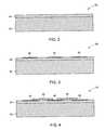
- FIG. 2is a cross-sectional view of a substrate coated with a dielectric layer
- FIG. 3is a cross-sectional view of nanowires deposited on the dielectric layer in FIG. 2 in accordance with embodiments of the present invention
- FIG. 4is a cross sectional view of a metal deposited on the nanowire deposited substrate in FIG. 3 ;
- FIG. 5is a cross-sectional view of a nanowire field effect transistor in accordance with embodiments of the present invention.
- FIG. 6is a cross-sectional view of a nanowire field effect transistor in accordance with embodiments of the present invention.
- FIG. 7is a flow chart illustrating exemplary steps in a method of depositing nanowires on a substrate in accordance with embodiments of the present invention.
- FIG. 8is a flow chart illustrating exemplary steps in a method of fabricating a nano field effect transistor on a substrate in accordance with embodiments of the present invention
- FIG. 9is a graphical representation of a transfer characteristic curve of the nanowire field effect transistor in FIG. 5 and FIG. 6 , illustrating variation of drain-source current as a function of gate voltage at different drain voltages;
- FIG. 10is a graphical representation of current in a nanowire p-n junction device as a function of voltage.
- nanostructuresrefers to a structure having a region or at least one characteristic dimension with a dimension of less than about 500 nm.
- the nanostructuresinclude nanowires, nanotubes, nanorods and quantum dots.
- nanostructuresmay be homogeneous or heterogeneous.
- the nanostructuremay be at least one of substantially crystalline, monocrystalline, polycrystalline, amorphous, or a combination thereof.
- the nanostructuresmay contain heterojunctions of different compositions or homojunctions of a same composition.
- the method of depositing nanostructuresis a modification of the Langmuir-Blodgett (LB) technique and may also be referred to, herein, as a “modified LB technique”.
- LBLangmuir-Blodgett
- the method disclosed hereinmay be used to manufacture any semiconductor device type and electronic component types. Further, the method may also be used in applications such as, but not limited to, electrical systems, optical systems and consumer electronics.
- FIG. 1is a schematic representation of a nanowire deposition system 10 .
- the system 10includes multiple nanowires 12 deposited onto a surface of a liquid 14 .
- the liquid 14may be deionized water.
- the liquid 14may be contained in a trough 16 .
- the trough 16may also be referred to as an “LB trough”.
- a trough barrier 18may be disposed on the surface of the liquid 14 to partially compress the nanowires 12 .
- An example of the trough barrier 18may include teflon.
- the nanowires 12may be partially compressed by depositing multiple spacer molecules between the nanowires 12 .
- the spacer moleculesmay also minimize agglomeration between the nanowires 12 .
- Some non-limiting examples of the spacer moleculesmay include 1-octadecylamine and self assembled monolayers. In another embodiment, there may be no spacer molecules between the nanowires on the water surface.
- a substrate 20may be dipped into the liquid 14 via multiple guide rollers 22 .
- the substrate 20may be a flexible substrate.
- the substrate 20may be a rigid substrate, which may be dipped into the liquid 14 without the use of rollers 22 .
- Some non-limiting examples of the substrate 20may include a glass, a polymer, a metal, and a semiconductor.
- the substrate 20may be pulled out of the liquid 14 at an opposite end of the trough 16 via rollers 22 .
- the nanowires 12are deposited onto a surface of the substrate 20 as the substrate 20 is pulled out of the liquid 14 , parallel to a direction of pulling via surface tension of the liquid 14 .
- Deposited nanowires 24are aligned in-plane of the substrate 20 .
- the rollers 22may be motored by a mechanical system 26 . Further, a control system 28 may automate the mechanical system 26 .
- a nanowire dispensing unit 29may be used to automatically disperse nanowires from a growth substrate into a solution and then dispense the nanowires 12 onto a surface of the liquid 14 .
- FIG. 2is a cross-sectional view of a system 30 including a substrate 32 that may be used in a nanoelectronic device array and depicts a first step in a process flow of metal deposition on nanowires that may be used in manufacturing the nanodevice array.
- a dielectric layer 34is deposited onto the substrate 32 .
- the dielectric layer 34may be deposited by chemical vapor deposition.
- the dielectric layer 34may be grown thermally.
- the dielectric layer 34may include silicon oxide, silicon nitride, aluminum oxide, zirconium oxide, and hafnium oxide.
- the substrate 32may include silicon, glass, a metal, a polymer or a combination thereof.
- FIG. 3is a cross-sectional view of a system 38 including nanowires 40 and illustrating a second step in the process flow of metal deposition.
- Multiple nanowires 40may be deposited onto the dielectric layer 34 .
- the nanowires 40may be deposited via the modified LB technique described above with reference to FIG. 1 .
- nanorodsmay be deposited onto the dielectric layer 34 .
- Some non-limiting examples of semiconductor types of materials for nanowiresmay include Si, Ge, Si—Ge, Sn-oxide, In-oxide, Se, Bi—Te, B, C, GaN, InGaN, AlGaN, ZnO, CdSe, CdTe, GaAs, AlAs, InSb, SiC, Mo 2 C, and a combination thereof.
- FIG. 4is a cross-sectional view of a system 44 illustrating a third step in the process flow of metal deposition.
- a metal 46may be deposited onto the nanowires 40 , and subsequently patterned, as illustrated.
- the metal 46may be deposited and patterned onto the nanowires 40 by photolithography.
- the metalmay include titanium, nickel, gold, aluminum, and palladium, and combinations thereof.
- FIG. 5a cross-sectional view of a field effect transistor (FET) 50 is depicted.
- the FET 50may be employed in an electronic device.
- an electronic device incorporating devices, such as the FET 50 , having nanostructures, such as nanowires,may also be referred to as a nanoelectronic device.
- the FET 50is manufactured using the modified LB technique of deposition of nanowires as discussed above.
- the FET 50may include a substrate 52 .
- Some non-limiting examples of the substrate 52may include glass and polymer.
- Multiple nanowires 54may be deposited onto the substrate 52 via the modified LB technique discussed with reference to FIG. 1 .
- a gate dielectric 56may be deposited onto the nanowires 54 .
- Some non-limiting examples of the gate dielectric 56may include silicon oxide, silicon nitride, aluminum oxide, zirconium oxide and hafnium oxide.
- a photoresist(not shown) may be deposited and patterned on the gate dielectric 56 in order to facilitate deposition and patterning of a source electrode 58 and a drain electrode 60 . In a particular embodiment, the photoresist is patterned via photolithography.
- the gate dielectric 56may further be etched to the nanowires 54 and the source electrode 58 and the drain electrode 60 may be formed onto the nanowires 54 .
- Some non-limiting examples of the source electrode 58 and the drain electrode 60may include titanium, gold, nickel and palladium.
- photoresistmay be employed in order to facilitate deposition and patterning of a gate electrode 62 on top of the gate dielectric 56 .
- FIG. 6is a cross-sectional view of an exemplary FET 70 in accordance with another embodiment of the invention.
- the FET 70may be an element of a large array of a nanoelectronic device.
- the FET 70includes a gate metal 72 as a substrate.
- Some non-limiting examples of the gate metal 72may include degenerately doped silicon.
- a gate dielectric 74may be deposited onto the gate metal 72 .
- Some non-limiting examples of the gate dielectric 74may include silicon oxide, silicon nitride, aluminum oxide, zirconium oxide and hafnium oxide.
- Multiple nanowires 76may further be deposited onto the gate dielectric 74 via the modified LB technique as described with reference to FIG. 1 .
- a photoresist(not shown) is deposited and patterned on top of the nanowires 76 in order to make space for a source electrode 78 and a drain electrode 80 .
- the photoresistis patterned via photolithography.
- the source electrode 78 and the drain electrode 80are then deposited onto the nanowires 76 , as illustrated in FIG. 6 .
- Some non-limiting examples of the source electrode 78 and the drain electrode 80may include titanium, gold, nickel and palladium
- FIG. 7is a flow chart illustrating exemplary steps in a method 90 for depositing nanowires.
- the method 90may include depositing a plurality of nanowires onto a surface of a liquid in step 92 .
- the nanowiresare partially compressed in step 94 .
- the nanowiresare partially compressed by depositing multiple spacer molecules between the nanowires.
- a substrateis dipped into the liquid in step 96 .
- the substrateis pulled out of the liquid at a controlled speed in step 98 .
- the substrateis dipped and pulled via multiple rollers.
- the controlled speedincludes a range between about 5 mm/min and 300 mm/min.
- the nanowiresare transferred onto the substrate parallel to a direction of the pulling in step 100 .
- the surface tension forces at the air-liquid interface and the rotational forces that occur as a result of the vertical pull of the substrate through the interfacegenerally facilitate alignment and transfer of the nanowires onto the surface of the substrate in parallel to the direction of the pull.
- the method 90 of the present inventionprovides certain improvements over conventional LB processes.
- the process of the present inventioninvolves the use of a partially compressed nanowire film, whereas in conventional LB processes, the film is compressed to substantially full density; that is, in the method of the present invention the nanowire film is compressed to some fraction of its theoretical density. In some embodiments, this fraction may range from about 5 percent to about 90 percent of an area of deposition of the nanowires on the substrate.
- the substrate withdrawal speedis controlled in the method of the present invention as described above.
- This speed controlcoupled with the use of a partially compressed film, results in the deposition of nanowires having an aligned orientation on the substrate, and the nanowire deposition may be done with improved control over the density of nanowire deposition compared with conventional processes.
- the nanowiresmay be deposited at a comparatively lower density than those typically achieved in conventional processes, which allows for deposition at precise locations for various passive and active electronic device applications.
- the alignment of the nanowires on the substratemay range within about +/ ⁇ 20 degrees enabling a yield of well-ordered arrays of nanoelectronic devices based on such nanowires.
- the method of the present inventionenables manufacturing of passive devices such as, but not limited to, display films and polarizers in addition to manufacturing functional electronics, sensor and optical nanodevice arrays.
- standing wavesmay be generated in the liquid in order to trap the nanowires against the surface of the substrate during the pull (step 98 ).
- the standing wavesmay be generated using ultrasonic agitation, for example.
- multiple magnetic electrodesmay be applied on the substrate and magnetic tips may be applied on the nanowires to create preferential attraction of the nanowires to the electrodes to enhance deposition and placement of the nanowires on the surface of the substrate.
- the substratemay be chemically treated in order to control placement of the nanowires in pre-defined locations of the substrate.
- a hydrophobic materialmay be used to treat areas of the substrate on which nanowires are not desired.
- Hydrophobic materialssuch as hexamethyldisilazane (HMDS), trimethlysilyl (TMS) or pentamethylsilyl (PMPS) or any other material that provides a methyl group residue.
- HMDShexamethyldisilazane
- TMStrimethlysilyl
- PMPSpentamethylsilyl
- any such area on the substrate treated with such materialwill be resistant to nanowire adhesion.
- materials that provide an amino group residuecould be used to treat areas where nanowire transfer is desirable, since the nanowires would be attracted to such materials.
- the use of such process enhancementsmay result in the nanowires disposed on the substrate in precise locations, allowing for more efficient device fabrication compared to the standard LB nanowire transfer process demonstrated in the art.
- FIG. 8is a flow chart illustrating exemplary steps in a method 110 for fabricating a nanoelectronic device array.
- the method 110includes depositing multiple nanowires onto a surface of a liquid in step 112 .
- the multiple nanowiresmay be partially compressed in step 114 .
- a substratemay be dipped into the liquid in step 116 .
- the substratemay be chemically treated and patterned to aide in the transfer of the nanowires to the desirable locations on the substrate.
- the substratemay be further pulled out of the liquid at a controlled speed in step 118 .
- the substrateis dipped and pulled via multiple rollers.
- the nanowiresmay be transferred onto the substrate being pulled parallel to a direction of the pulling in step 120 .
- standing wavesmay be generated in the liquid in order to trap the nanowires.
- the nanowiresmay be transferred onto the substrate by surface tension of the liquid.
- a source electrodemay be formed on the nanowires in step 122 .
- a drain electrodemay also be formed on the nanowires in step 124 .
- the source electrode and the drain electrodemay be formed in a single step.
- a gate electrodemay be further formed in step 126 .
- a photoresistis patterned via a process such as, but not limited to, photolithography on top of the nanowires prior to depositing the source electrode and the drain electrode.
- a gate dielectricmay be deposited on the gate electrode.
- the gate dielectricmay be deposited on the nanowires.
- the method 110may include fabricating a nano field effect transistor array, a nano p-n junction device array, a nanoelectronic logic circuit array, a nanoscale chemical, physical, or biological sensor array, a nanoelectromechanical device array, or a photodetector array.
- FIG. 9is a graphical representation of a transfer characteristic curve 140 of a nanowire FET fabricated as in FIG. 5 and FIG. 6 . Electrodes of the nanowire FET were fabricated by standard photolithography and lift-off process. The nanowires were grown using a low-pressure chemical vapor deposition (LPCVD) system by flowing silane, hydrogen, hydrochloric acid, and trimethylboron.
- the X-axis 142represents gate voltage in volts.
- the Y-axis 144represents drain current in amperes.
- Curve 146represents variation of drain current as a function of gate voltage at a constant drain voltage of 0.1V.
- curves 148 , 150 , 152 , 154 , 156 , 158 , 160 , 162 and 164represent variation of drain current as a function of gate voltage at drain voltages of 0.3V, 0.5V, 0.7V, 0.9V, 1.1V, 1.3V, 1.5V, 1.7V, and 1.9V respectively.
- a functional nanowire FETmay be fabricated using the modified LB technique as discussed above.
- FIG. 10is a graphical representation of a current-voltage relationship curve 170 in a nanowire p-n junction device fabricated in accordance with an embodiment of the invention.
- Nanowireswere grown using a LPCVD system by flowing silane, hydrogen, hydrochloric acid, and trimethylboron for a p-type segment followed by flowing phosphine in place of trimethylboron for an n-type segment of the nanowire p-n junction device.
- the p-n junction deviceincluded multiple longitudinal p-n junctions.
- X-axis 172represents voltage in volts.
- Y-axis 174represents current in amperes.
- Curve 176shows variation of the current as a function of the voltage and matches a conventional current-voltage curve that is seen in a functional p-n device. Thus, the curve 176 demonstrates a functional p-n device that has been fabricated using the modified LB technique as discussed above.
Landscapes
- Engineering & Computer Science (AREA)
- Physics & Mathematics (AREA)
- Chemical & Material Sciences (AREA)
- Microelectronics & Electronic Packaging (AREA)
- Manufacturing & Machinery (AREA)
- Computer Hardware Design (AREA)
- General Physics & Mathematics (AREA)
- Power Engineering (AREA)
- Condensed Matter Physics & Semiconductors (AREA)
- Nanotechnology (AREA)
- Crystallography & Structural Chemistry (AREA)
- Mathematical Physics (AREA)
- Theoretical Computer Science (AREA)
- Thin Film Transistor (AREA)
Abstract
Description
- The invention relates generally to nanowires, and, more particularly, to techniques for depositing nanowires and techniques for assembling electronic devices incorporating nanowires.
- Nanostructures, and in particular, nanowires are known to have the potential to facilitate a new generation of electronic devices. Significant progress has been made in the area of nanowire synthesis and device application over past several years. Assembly of the nanowires is a critical factor in forming a functional electronic system. In order to effectively employ nanowires in most of the areas of nanotechnology, a controlled and predictable assembly of aligned nanostructures is desirable.
- Various assembly techniques have been employed for alignment of the nanowires. Some of the commonly used techniques include direct growth methods for synthesis of nanowires in specific locations and post growth assembly techniques such as microfluidic assembly, electric field assembly, chemical patterning and Langmuir-Blodgett assembly. One specific technique is to apply Langmuir-Blodgett (LB) alignment techniques to align nanowires. The LB technique allows transfer of nanowire monolayers that are fully compressed, from a surface of water to a solid substrate by slowly passing a substrate through an air-water interface. The LB technique may also be used to assemble large area nanowire monolayers.
- However, the existing assembly techniques have not been useful in yielding a controlled in-plane alignment and patterning of the nanowires that would make a significant impact in a wide variety of applications such as nanoscale electronics, optoelectronics and molecular sensing. Further, a major impediment to the emergence of a new generation of electronic devices based on nanostructures has been the inability to effectively grow and harvest nanowires that have consistent performance characteristics. Current techniques have not yielded desirable performance characteristics.
- Accordingly, an improved assembly technique is needed to address one or more of the foregoing issues.
- In accordance with one aspect of the invention, a method for depositing nanowires is provided. The method includes depositing a plurality of nanowires onto a surface of a liquid. The method also includes partially compressing the plurality of nanowires. The method also includes dipping a substrate into the liquid. The method further includes pulling the substrate out of the liquid at a controlled speed. The method also includes transferring the plurality of nanowires onto the substrate parallel to a direction of the pulling.
- In accordance with another aspect of the invention, an electronic device is provided. The electronic device includes multiple nanowires disposed on a substrate and aligned in a single direction on the substrate within a range of about +/−20 degrees and having a density ranging between about 5 percent and about 90 percent of an area of deposition of the plurality of nanowires on the substrate.
- In accordance with another aspect of the invention, a method of fabricating a nano field effect transistor is provided. The method includes depositing multiple nanowires onto a surface of a liquid. The method also includes partially compressing the nanowires. The method also includes dipping a substrate into the liquid. The method further includes pulling the substrate out of the liquid at a controlled speed. The method also includes transferring the nanowires onto the substrate parallel to a direction of the pulling. The method also includes forming a source electrode on the nanowires. The method further includes forming a drain electrode on the nanowires. The method further includes forming a gate electrode.
- In accordance with another aspect of the invention, a system for depositing nanowires is provided. The system includes a trough configured to contain a liquid. The system also includes multiple rollers configured to move a flexible substrate through the trough containing the liquid. The system further includes a nanowire dispensing unit configured to deposit a plurality of nanowires onto a surface of the liquid. The system also includes a barrier configured to compress the plurality of nanowires.
- These and other features, aspects, and advantages of the present invention will become better understood when the following detailed description is read with reference to the accompanying drawings in which like characters represent like parts throughout the drawings, wherein:
FIG. 1 is a schematic representation of a nanowire deposition system in accordance with embodiments of the present invention;FIG. 2 is a cross-sectional view of a substrate coated with a dielectric layer;FIG. 3 is a cross-sectional view of nanowires deposited on the dielectric layer inFIG. 2 in accordance with embodiments of the present invention;FIG. 4 is a cross sectional view of a metal deposited on the nanowire deposited substrate inFIG. 3 ;FIG. 5 is a cross-sectional view of a nanowire field effect transistor in accordance with embodiments of the present invention;FIG. 6 is a cross-sectional view of a nanowire field effect transistor in accordance with embodiments of the present invention;FIG. 7 is a flow chart illustrating exemplary steps in a method of depositing nanowires on a substrate in accordance with embodiments of the present invention.FIG. 8 is a flow chart illustrating exemplary steps in a method of fabricating a nano field effect transistor on a substrate in accordance with embodiments of the present invention;FIG. 9 is a graphical representation of a transfer characteristic curve of the nanowire field effect transistor inFIG. 5 andFIG. 6 , illustrating variation of drain-source current as a function of gate voltage at different drain voltages; andFIG. 10 is a graphical representation of current in a nanowire p-n junction device as a function of voltage.- As described in detail below, embodiments of the present invention include nanostructures, methods of depositing nanostructures and devices incorporating the same. As used herein, the term “nanostructures” refers to a structure having a region or at least one characteristic dimension with a dimension of less than about 500 nm. Some non-limiting examples of the nanostructures include nanowires, nanotubes, nanorods and quantum dots. In terms of material properties, nanostructures may be homogeneous or heterogeneous. In an example, the nanostructure may be at least one of substantially crystalline, monocrystalline, polycrystalline, amorphous, or a combination thereof. In another example, the nanostructures may contain heterojunctions of different compositions or homojunctions of a same composition. The method of depositing nanostructures is a modification of the Langmuir-Blodgett (LB) technique and may also be referred to, herein, as a “modified LB technique”. The method disclosed herein may be used to manufacture any semiconductor device type and electronic component types. Further, the method may also be used in applications such as, but not limited to, electrical systems, optical systems and consumer electronics.
- Turning now to the drawings,
FIG. 1 is a schematic representation of ananowire deposition system 10. The process will be described in more detail below with reference toFIGS. 7 and 8 . Thesystem 10 includesmultiple nanowires 12 deposited onto a surface of aliquid 14. In an example, theliquid 14 may be deionized water. Theliquid 14 may be contained in atrough 16. Thetrough 16 may also be referred to as an “LB trough”. Atrough barrier 18 may be disposed on the surface of the liquid14 to partially compress thenanowires 12. An example of thetrough barrier 18 may include teflon. In a particular embodiment, thenanowires 12 may be partially compressed by depositing multiple spacer molecules between thenanowires 12. The spacer molecules may also minimize agglomeration between thenanowires 12. Some non-limiting examples of the spacer molecules may include 1-octadecylamine and self assembled monolayers. In another embodiment, there may be no spacer molecules between the nanowires on the water surface. Asubstrate 20 may be dipped into the liquid14 viamultiple guide rollers 22. In a particular embodiment, thesubstrate 20 may be a flexible substrate. In another embodiment, thesubstrate 20 may be a rigid substrate, which may be dipped into the liquid14 without the use ofrollers 22. Some non-limiting examples of thesubstrate 20 may include a glass, a polymer, a metal, and a semiconductor. Thesubstrate 20 may be pulled out of the liquid14 at an opposite end of thetrough 16 viarollers 22. Thenanowires 12 are deposited onto a surface of thesubstrate 20 as thesubstrate 20 is pulled out of the liquid14, parallel to a direction of pulling via surface tension of the liquid14. Depositednanowires 24 are aligned in-plane of thesubstrate 20. Therollers 22 may be motored by amechanical system 26. Further, acontrol system 28 may automate themechanical system 26. In a particular embodiment, ananowire dispensing unit 29 may be used to automatically disperse nanowires from a growth substrate into a solution and then dispense thenanowires 12 onto a surface of the liquid14. FIG. 2 is a cross-sectional view of asystem 30 including asubstrate 32 that may be used in a nanoelectronic device array and depicts a first step in a process flow of metal deposition on nanowires that may be used in manufacturing the nanodevice array. Adielectric layer 34 is deposited onto thesubstrate 32. In a particular embodiment, thedielectric layer 34 may be deposited by chemical vapor deposition. In another embodiment, thedielectric layer 34 may be grown thermally. In an example, thedielectric layer 34 may include silicon oxide, silicon nitride, aluminum oxide, zirconium oxide, and hafnium oxide. Some non-limiting examples of thesubstrate 32 may include silicon, glass, a metal, a polymer or a combination thereof.FIG. 3 is a cross-sectional view of asystem 38 includingnanowires 40 and illustrating a second step in the process flow of metal deposition.Multiple nanowires 40 may be deposited onto thedielectric layer 34. In a particular embodiment, thenanowires 40 may be deposited via the modified LB technique described above with reference toFIG. 1 . In another embodiment, nanorods may be deposited onto thedielectric layer 34. Some non-limiting examples of semiconductor types of materials for nanowires may include Si, Ge, Si—Ge, Sn-oxide, In-oxide, Se, Bi—Te, B, C, GaN, InGaN, AlGaN, ZnO, CdSe, CdTe, GaAs, AlAs, InSb, SiC, Mo2C, and a combination thereof.FIG. 4 is a cross-sectional view of asystem 44 illustrating a third step in the process flow of metal deposition. Once thenanowires 40 are deposited as shown inFIG. 3 , ametal 46 may be deposited onto thenanowires 40, and subsequently patterned, as illustrated. In a particular embodiment, themetal 46 may be deposited and patterned onto thenanowires 40 by photolithography. Some non-limiting examples of the metal may include titanium, nickel, gold, aluminum, and palladium, and combinations thereof.- In another illustrated embodiment of the invention as shown in
FIG. 5 , a cross-sectional view of a field effect transistor (FET)50 is depicted. As will be appreciated, theFET 50 may be employed in an electronic device. As used herein, an electronic device incorporating devices, such as theFET 50, having nanostructures, such as nanowires, may also be referred to as a nanoelectronic device. TheFET 50 is manufactured using the modified LB technique of deposition of nanowires as discussed above. TheFET 50 may include asubstrate 52. Some non-limiting examples of thesubstrate 52 may include glass and polymer.Multiple nanowires 54 may be deposited onto thesubstrate 52 via the modified LB technique discussed with reference toFIG. 1 . Agate dielectric 56 may be deposited onto thenanowires 54. Some non-limiting examples of thegate dielectric 56 may include silicon oxide, silicon nitride, aluminum oxide, zirconium oxide and hafnium oxide. A photoresist (not shown) may be deposited and patterned on thegate dielectric 56 in order to facilitate deposition and patterning of asource electrode 58 and adrain electrode 60. In a particular embodiment, the photoresist is patterned via photolithography. Thegate dielectric 56 may further be etched to thenanowires 54 and thesource electrode 58 and thedrain electrode 60 may be formed onto thenanowires 54. Some non-limiting examples of thesource electrode 58 and thedrain electrode 60 may include titanium, gold, nickel and palladium. Similarly, photoresist may be employed in order to facilitate deposition and patterning of agate electrode 62 on top of thegate dielectric 56. FIG. 6 is a cross-sectional view of anexemplary FET 70 in accordance with another embodiment of the invention. In a particular embodiment, theFET 70 may be an element of a large array of a nanoelectronic device. TheFET 70 includes agate metal 72 as a substrate. Some non-limiting examples of thegate metal 72 may include degenerately doped silicon. Agate dielectric 74 may be deposited onto thegate metal 72. Some non-limiting examples of thegate dielectric 74 may include silicon oxide, silicon nitride, aluminum oxide, zirconium oxide and hafnium oxide. Multiple nanowires76 may further be deposited onto thegate dielectric 74 via the modified LB technique as described with reference toFIG. 1 . A photoresist (not shown) is deposited and patterned on top of the nanowires76 in order to make space for asource electrode 78 and adrain electrode 80. In a particular embodiment, the photoresist is patterned via photolithography. Thesource electrode 78 and thedrain electrode 80 are then deposited onto the nanowires76, as illustrated inFIG. 6 . Some non-limiting examples of thesource electrode 78 and thedrain electrode 80 may include titanium, gold, nickel and palladiumFIG. 7 is a flow chart illustrating exemplary steps in amethod 90 for depositing nanowires. Themethod 90 may include depositing a plurality of nanowires onto a surface of a liquid instep 92. The nanowires are partially compressed instep 94. In a particular embodiment, the nanowires are partially compressed by depositing multiple spacer molecules between the nanowires. A substrate is dipped into the liquid instep 96. The substrate is pulled out of the liquid at a controlled speed instep 98. In an exemplary embodiment, the substrate is dipped and pulled via multiple rollers. In another embodiment, the controlled speed includes a range between about 5 mm/min and 300 mm/min. During the process of pulling instep 98, the nanowires are transferred onto the substrate parallel to a direction of the pulling instep 100. In particular, the surface tension forces at the air-liquid interface and the rotational forces that occur as a result of the vertical pull of the substrate through the interface generally facilitate alignment and transfer of the nanowires onto the surface of the substrate in parallel to the direction of the pull.- The
method 90 of the present invention provides certain improvements over conventional LB processes. For example, as described above, the process of the present invention involves the use of a partially compressed nanowire film, whereas in conventional LB processes, the film is compressed to substantially full density; that is, in the method of the present invention the nanowire film is compressed to some fraction of its theoretical density. In some embodiments, this fraction may range from about 5 percent to about 90 percent of an area of deposition of the nanowires on the substrate. Moreover, the substrate withdrawal speed is controlled in the method of the present invention as described above. This speed control, coupled with the use of a partially compressed film, results in the deposition of nanowires having an aligned orientation on the substrate, and the nanowire deposition may be done with improved control over the density of nanowire deposition compared with conventional processes. For example, the nanowires may be deposited at a comparatively lower density than those typically achieved in conventional processes, which allows for deposition at precise locations for various passive and active electronic device applications. Furthermore, the alignment of the nanowires on the substrate may range within about +/−20 degrees enabling a yield of well-ordered arrays of nanoelectronic devices based on such nanowires. Thus, the method of the present invention enables manufacturing of passive devices such as, but not limited to, display films and polarizers in addition to manufacturing functional electronics, sensor and optical nanodevice arrays. - Various techniques may be employed in conjunction with the process, in order to aid in the transfer of nanowires onto the surface of the substrate. For example, in one particular embodiment, standing waves may be generated in the liquid in order to trap the nanowires against the surface of the substrate during the pull (step98). The standing waves may be generated using ultrasonic agitation, for example. In another embodiment, multiple magnetic electrodes may be applied on the substrate and magnetic tips may be applied on the nanowires to create preferential attraction of the nanowires to the electrodes to enhance deposition and placement of the nanowires on the surface of the substrate. Further, in another embodiment, the substrate may be chemically treated in order to control placement of the nanowires in pre-defined locations of the substrate. For instance, a hydrophobic material may be used to treat areas of the substrate on which nanowires are not desired. Hydrophobic materials, such as hexamethyldisilazane (HMDS), trimethlysilyl (TMS) or pentamethylsilyl (PMPS) or any other material that provides a methyl group residue. As will be appreciated, any such area on the substrate treated with such material will be resistant to nanowire adhesion. Alternatively, materials that provide an amino group residue could be used to treat areas where nanowire transfer is desirable, since the nanowires would be attracted to such materials. The use of such process enhancements may result in the nanowires disposed on the substrate in precise locations, allowing for more efficient device fabrication compared to the standard LB nanowire transfer process demonstrated in the art.
FIG. 8 is a flow chart illustrating exemplary steps in amethod 110 for fabricating a nanoelectronic device array. Themethod 110 includes depositing multiple nanowires onto a surface of a liquid instep 112. The multiple nanowires may be partially compressed instep 114. A substrate may be dipped into the liquid instep 116. As described above, the substrate may be chemically treated and patterned to aide in the transfer of the nanowires to the desirable locations on the substrate. The substrate may be further pulled out of the liquid at a controlled speed instep 118. In an exemplary embodiment, the substrate is dipped and pulled via multiple rollers. The nanowires may be transferred onto the substrate being pulled parallel to a direction of the pulling instep 120. In a particular embodiment, standing waves may be generated in the liquid in order to trap the nanowires. In another embodiment, the nanowires may be transferred onto the substrate by surface tension of the liquid. A source electrode may be formed on the nanowires instep 122. A drain electrode may also be formed on the nanowires instep 124. In a preferred embodiment, the source electrode and the drain electrode may be formed in a single step. A gate electrode may be further formed instep 126. In a particular embodiment, a photoresist is patterned via a process such as, but not limited to, photolithography on top of the nanowires prior to depositing the source electrode and the drain electrode. In another embodiment, a gate dielectric may be deposited on the gate electrode. In yet another embodiment, the gate dielectric may be deposited on the nanowires. In a particular embodiment, themethod 110 may include fabricating a nano field effect transistor array, a nano p-n junction device array, a nanoelectronic logic circuit array, a nanoscale chemical, physical, or biological sensor array, a nanoelectromechanical device array, or a photodetector array.- The examples that follow are merely illustrative, and should not be construed to be any sort of limitation on the scope of the claimed invention.
FIG. 9 is a graphical representation of a transfercharacteristic curve 140 of a nanowire FET fabricated as inFIG. 5 andFIG. 6 . Electrodes of the nanowire FET were fabricated by standard photolithography and lift-off process. The nanowires were grown using a low-pressure chemical vapor deposition (LPCVD) system by flowing silane, hydrogen, hydrochloric acid, and trimethylboron. TheX-axis 142 represents gate voltage in volts. The Y-axis 144 represents drain current in amperes.Curve 146 represents variation of drain current as a function of gate voltage at a constant drain voltage of 0.1V. Similarly, curves148,150,152,154,156,158,160,162 and164 represent variation of drain current as a function of gate voltage at drain voltages of 0.3V, 0.5V, 0.7V, 0.9V, 1.1V, 1.3V, 1.5V, 1.7V, and 1.9V respectively. Thus, it can be seen from the curves that a functional nanowire FET may be fabricated using the modified LB technique as discussed above.FIG. 10 is a graphical representation of a current-voltage relationship curve 170 in a nanowire p-n junction device fabricated in accordance with an embodiment of the invention. Nanowires were grown using a LPCVD system by flowing silane, hydrogen, hydrochloric acid, and trimethylboron for a p-type segment followed by flowing phosphine in place of trimethylboron for an n-type segment of the nanowire p-n junction device. The p-n junction device included multiple longitudinal p-n junctions.X-axis 172 represents voltage in volts. Y-axis 174 represents current in amperes.Curve 176 shows variation of the current as a function of the voltage and matches a conventional current-voltage curve that is seen in a functional p-n device. Thus, thecurve 176 demonstrates a functional p-n device that has been fabricated using the modified LB technique as discussed above.- While only certain features of the invention have been illustrated and described herein, many modifications and changes will occur to those skilled in the art. It is, therefore, to be understood that the appended claims are intended to cover all such modifications and changes as fall within the true spirit of the invention.
Claims (32)
Priority Applications (1)
| Application Number | Priority Date | Filing Date | Title |
|---|---|---|---|
| US11/633,205US8258047B2 (en) | 2006-12-04 | 2006-12-04 | Nanostructures, methods of depositing nanostructures and devices incorporating the same |
Applications Claiming Priority (1)
| Application Number | Priority Date | Filing Date | Title |
|---|---|---|---|
| US11/633,205US8258047B2 (en) | 2006-12-04 | 2006-12-04 | Nanostructures, methods of depositing nanostructures and devices incorporating the same |
Publications (2)
| Publication Number | Publication Date |
|---|---|
| US20100261338A1true US20100261338A1 (en) | 2010-10-14 |
| US8258047B2 US8258047B2 (en) | 2012-09-04 |
Family
ID=42934735
Family Applications (1)
| Application Number | Title | Priority Date | Filing Date |
|---|---|---|---|
| US11/633,205Expired - Fee RelatedUS8258047B2 (en) | 2006-12-04 | 2006-12-04 | Nanostructures, methods of depositing nanostructures and devices incorporating the same |
Country Status (1)
| Country | Link |
|---|---|
| US (1) | US8258047B2 (en) |
Cited By (14)
| Publication number | Priority date | Publication date | Assignee | Title |
|---|---|---|---|---|
| US20090139752A1 (en)* | 2007-10-11 | 2009-06-04 | Riken | Electronic device and method for producing electronic device |
| US20100301308A1 (en)* | 2009-05-26 | 2010-12-02 | University Of Seoul Industry Cooperation Foundation | Photodetectors |
| US20100326489A1 (en)* | 2009-06-29 | 2010-12-30 | University Of Seoul Industry Cooperation Foundation | Light-electricity conversion device |
| US20110001124A1 (en)* | 2009-07-06 | 2011-01-06 | University Of Seoul Industry Cooperation Foundation | Photodetector capable of detecting the visible light spectrum |
| US20110001125A1 (en)* | 2009-07-06 | 2011-01-06 | University Of Seoul Industry Cooperation Foundation | Photodetector capable of detecting long wavelength radiation |
| US20110043884A1 (en)* | 2009-08-21 | 2011-02-24 | University Of Seoul Industry Cooperation Foundation | Polariton mode optical switch with composite structure |
| US20110095309A1 (en)* | 2009-10-27 | 2011-04-28 | University Of Seoul Industry Cooperation Foundation | Semiconductor device |
| US8395141B2 (en) | 2009-07-06 | 2013-03-12 | University Of Seoul Industry Cooperation Foundation | Compound semiconductors |
| US8524517B2 (en) | 2009-11-18 | 2013-09-03 | University Of Seoul Industry Cooperation Foundation | Copper blend I-VII compound semiconductor light-emitting devices |
| ES2407582R1 (en)* | 2011-07-19 | 2013-10-11 | Univ Salamanca | DEVICE AND PROCEDURE FOR EFFECTING A LANGMUIR-BLODGETT COATING IN A TEXTILE MATERIAL |
| US8748862B2 (en) | 2009-07-06 | 2014-06-10 | University Of Seoul Industry Cooperation Foundation | Compound semiconductors |
| WO2015084805A1 (en)* | 2013-12-03 | 2015-06-11 | President And Fellows Of Harvard College | Nanoscale wire probes for the brain and other applications |
| CN108701618A (en)* | 2016-03-30 | 2018-10-23 | 英特尔公司 | The nano wire integrated for transistor |
| US10163932B1 (en)* | 2015-07-24 | 2018-12-25 | Nutech Ventures | Memory device based on heterostructures of ferroelectric and two-dimensional materials |
Citations (18)
| Publication number | Priority date | Publication date | Assignee | Title |
|---|---|---|---|---|
| US5280183A (en)* | 1988-05-31 | 1994-01-18 | Edison Polymer Innovation Corporation | Microelectronic device employing multiring phthalocyanine compound |
| US5688562A (en)* | 1995-06-20 | 1997-11-18 | E. I. Du Pont De Nemours And Company | Method for modifying uncoated synthetic polymer fibers using a Langmuir-Blodgett film coating process |
| US6036778A (en)* | 1997-05-30 | 2000-03-14 | Canon Kabushiki Kaisha | Apparatus for producing Langmuir-Blodgett film |
| US20020130211A1 (en)* | 2001-11-15 | 2002-09-19 | Browne & Co.Ltd. | Holding device for paper towel and napkin holder |
| US6536106B1 (en)* | 1999-06-30 | 2003-03-25 | The Penn State Research Foundation | Electric field assisted assembly process |
| US20030089899A1 (en)* | 2000-08-22 | 2003-05-15 | Lieber Charles M. | Nanoscale wires and related devices |
| US20030186522A1 (en)* | 2002-04-02 | 2003-10-02 | Nanosys, Inc. | Methods of positioning and/or orienting nanostructures |
| US20040137220A1 (en)* | 2003-01-14 | 2004-07-15 | Hitachi, Ltd. | Method for producing nanoparticle layer having uniform easy axis of magnetization, magnetic recording medium having such layer, its production method, and its production apparatus |
| US20050066883A1 (en)* | 2003-09-25 | 2005-03-31 | Nanosys, Inc. | Methods, devices and compositions for depositing and orienting nanostructures |
| US20050110064A1 (en)* | 2002-09-30 | 2005-05-26 | Nanosys, Inc. | Large-area nanoenabled macroelectronic substrates and uses therefor |
| US20050164432A1 (en)* | 2000-08-22 | 2005-07-28 | President And Fellows Of Harvard College | Doped elongated semiconductors, growing such semiconductors, devices including such semiconductors and fabricating such devices |
| US20050181587A1 (en)* | 2002-09-30 | 2005-08-18 | Nanosys, Inc. | Large-area nanoenabled macroelectronic substrates and uses therefor |
| US20050279274A1 (en)* | 2004-04-30 | 2005-12-22 | Chunming Niu | Systems and methods for nanowire growth and manufacturing |
| US20060008942A1 (en)* | 2004-07-07 | 2006-01-12 | Nanosys, Inc. | Systems and methods for harvesting and integrating nanowires |
| US20060105513A1 (en)* | 2004-11-18 | 2006-05-18 | International Business Machines Corporation | Device comprising doped nano-component and method of forming the device |
| US20060148166A1 (en)* | 2004-11-08 | 2006-07-06 | Craig Gordon S | Assembly comprising functional devices and method of making same |
| US20070155025A1 (en)* | 2006-01-04 | 2007-07-05 | Anping Zhang | Nanowire structures and devices for use in large-area electronics and methods of making the same |
| US20080083950A1 (en)* | 2006-10-10 | 2008-04-10 | Alfred I-Tsung Pan | Fused nanocrystal thin film semiconductor and method |
- 2006
- 2006-12-04USUS11/633,205patent/US8258047B2/ennot_activeExpired - Fee Related
Patent Citations (23)
| Publication number | Priority date | Publication date | Assignee | Title |
|---|---|---|---|---|
| US5280183A (en)* | 1988-05-31 | 1994-01-18 | Edison Polymer Innovation Corporation | Microelectronic device employing multiring phthalocyanine compound |
| US5688562A (en)* | 1995-06-20 | 1997-11-18 | E. I. Du Pont De Nemours And Company | Method for modifying uncoated synthetic polymer fibers using a Langmuir-Blodgett film coating process |
| US6036778A (en)* | 1997-05-30 | 2000-03-14 | Canon Kabushiki Kaisha | Apparatus for producing Langmuir-Blodgett film |
| US6536106B1 (en)* | 1999-06-30 | 2003-03-25 | The Penn State Research Foundation | Electric field assisted assembly process |
| US20050164432A1 (en)* | 2000-08-22 | 2005-07-28 | President And Fellows Of Harvard College | Doped elongated semiconductors, growing such semiconductors, devices including such semiconductors and fabricating such devices |
| US20070026645A1 (en)* | 2000-08-22 | 2007-02-01 | President And Fellows Of Harvard College | Doped elongated semiconductors, growing such semiconductors, devices including such semiconductors, and fabricating such devices |
| US20030089899A1 (en)* | 2000-08-22 | 2003-05-15 | Lieber Charles M. | Nanoscale wires and related devices |
| US20020130211A1 (en)* | 2001-11-15 | 2002-09-19 | Browne & Co.Ltd. | Holding device for paper towel and napkin holder |
| US20030186522A1 (en)* | 2002-04-02 | 2003-10-02 | Nanosys, Inc. | Methods of positioning and/or orienting nanostructures |
| US20060151820A1 (en)* | 2002-09-30 | 2006-07-13 | Nanosys, Inc. | Large-area nanoenabled macroelectronic substrates and uses therefor |
| US20060211183A1 (en)* | 2002-09-30 | 2006-09-21 | Nanosys, Inc. | Large-area nanoenabled macroelectronic substrates and uses therefor |
| US20050181587A1 (en)* | 2002-09-30 | 2005-08-18 | Nanosys, Inc. | Large-area nanoenabled macroelectronic substrates and uses therefor |
| US20050110064A1 (en)* | 2002-09-30 | 2005-05-26 | Nanosys, Inc. | Large-area nanoenabled macroelectronic substrates and uses therefor |
| US7064372B2 (en)* | 2002-09-30 | 2006-06-20 | Nanosys, Inc. | Large-area nanoenabled macroelectronic substrates and uses therefor |
| US7135728B2 (en)* | 2002-09-30 | 2006-11-14 | Nanosys, Inc. | Large-area nanoenabled macroelectronic substrates and uses therefor |
| US20040137220A1 (en)* | 2003-01-14 | 2004-07-15 | Hitachi, Ltd. | Method for producing nanoparticle layer having uniform easy axis of magnetization, magnetic recording medium having such layer, its production method, and its production apparatus |
| US20050066883A1 (en)* | 2003-09-25 | 2005-03-31 | Nanosys, Inc. | Methods, devices and compositions for depositing and orienting nanostructures |
| US20050279274A1 (en)* | 2004-04-30 | 2005-12-22 | Chunming Niu | Systems and methods for nanowire growth and manufacturing |
| US20060008942A1 (en)* | 2004-07-07 | 2006-01-12 | Nanosys, Inc. | Systems and methods for harvesting and integrating nanowires |
| US20060148166A1 (en)* | 2004-11-08 | 2006-07-06 | Craig Gordon S | Assembly comprising functional devices and method of making same |
| US20060105513A1 (en)* | 2004-11-18 | 2006-05-18 | International Business Machines Corporation | Device comprising doped nano-component and method of forming the device |
| US20070155025A1 (en)* | 2006-01-04 | 2007-07-05 | Anping Zhang | Nanowire structures and devices for use in large-area electronics and methods of making the same |
| US20080083950A1 (en)* | 2006-10-10 | 2008-04-10 | Alfred I-Tsung Pan | Fused nanocrystal thin film semiconductor and method |
Cited By (27)
| Publication number | Priority date | Publication date | Assignee | Title |
|---|---|---|---|---|
| US8043978B2 (en)* | 2007-10-11 | 2011-10-25 | Riken | Electronic device and method for producing electronic device |
| US20090139752A1 (en)* | 2007-10-11 | 2009-06-04 | Riken | Electronic device and method for producing electronic device |
| US20100301308A1 (en)* | 2009-05-26 | 2010-12-02 | University Of Seoul Industry Cooperation Foundation | Photodetectors |
| US8373153B2 (en) | 2009-05-26 | 2013-02-12 | University Of Seoul Industry Cooperation Foundation | Photodetectors |
| US20100326489A1 (en)* | 2009-06-29 | 2010-12-30 | University Of Seoul Industry Cooperation Foundation | Light-electricity conversion device |
| US8367925B2 (en) | 2009-06-29 | 2013-02-05 | University Of Seoul Industry Cooperation Foundation | Light-electricity conversion device |
| US8802481B2 (en) | 2009-07-06 | 2014-08-12 | University Of Seoul Industry Cooperation Foundation | Photodetector capable of detecting the visible light spectrum |
| US8748862B2 (en) | 2009-07-06 | 2014-06-10 | University Of Seoul Industry Cooperation Foundation | Compound semiconductors |
| US8227793B2 (en)* | 2009-07-06 | 2012-07-24 | University Of Seoul Industry Cooperation Foundation | Photodetector capable of detecting the visible light spectrum |
| US9397249B2 (en) | 2009-07-06 | 2016-07-19 | University Of Seoul Industry Cooperation Foundation | Photodetector capable of detecting long wavelength radiation |
| US8809834B2 (en) | 2009-07-06 | 2014-08-19 | University Of Seoul Industry Cooperation Foundation | Photodetector capable of detecting long wavelength radiation |
| US20110001124A1 (en)* | 2009-07-06 | 2011-01-06 | University Of Seoul Industry Cooperation Foundation | Photodetector capable of detecting the visible light spectrum |
| US20110001125A1 (en)* | 2009-07-06 | 2011-01-06 | University Of Seoul Industry Cooperation Foundation | Photodetector capable of detecting long wavelength radiation |
| US8395141B2 (en) | 2009-07-06 | 2013-03-12 | University Of Seoul Industry Cooperation Foundation | Compound semiconductors |
| US8368990B2 (en) | 2009-08-21 | 2013-02-05 | University Of Seoul Industry Cooperation Foundation | Polariton mode optical switch with composite structure |
| US8681411B2 (en) | 2009-08-21 | 2014-03-25 | University Of Seoul Industry Cooperation Foundation | Polariton mode optical switch with composite structure |
| US20110043884A1 (en)* | 2009-08-21 | 2011-02-24 | University Of Seoul Industry Cooperation Foundation | Polariton mode optical switch with composite structure |
| US20110095309A1 (en)* | 2009-10-27 | 2011-04-28 | University Of Seoul Industry Cooperation Foundation | Semiconductor device |
| US8368047B2 (en) | 2009-10-27 | 2013-02-05 | University Of Seoul Industry Cooperation Foundation | Semiconductor device |
| US8524517B2 (en) | 2009-11-18 | 2013-09-03 | University Of Seoul Industry Cooperation Foundation | Copper blend I-VII compound semiconductor light-emitting devices |
| ES2407582R1 (en)* | 2011-07-19 | 2013-10-11 | Univ Salamanca | DEVICE AND PROCEDURE FOR EFFECTING A LANGMUIR-BLODGETT COATING IN A TEXTILE MATERIAL |
| WO2015084805A1 (en)* | 2013-12-03 | 2015-06-11 | President And Fellows Of Harvard College | Nanoscale wire probes for the brain and other applications |
| US20160302682A1 (en)* | 2013-12-03 | 2016-10-20 | President And Fellows Of Harvard College | Nanoscale wire probes for the brain and other applications |
| US10163932B1 (en)* | 2015-07-24 | 2018-12-25 | Nutech Ventures | Memory device based on heterostructures of ferroelectric and two-dimensional materials |
| CN108701618A (en)* | 2016-03-30 | 2018-10-23 | 英特尔公司 | The nano wire integrated for transistor |
| US11588017B2 (en)* | 2016-03-30 | 2023-02-21 | Intel Corporation | Nanowire for transistor integration |
| CN108701618B (en)* | 2016-03-30 | 2023-02-28 | 英特尔公司 | Nanowires for transistor integration |
Also Published As
| Publication number | Publication date |
|---|---|
| US8258047B2 (en) | 2012-09-04 |
Similar Documents
| Publication | Publication Date | Title |
|---|---|---|
| US8258047B2 (en) | Nanostructures, methods of depositing nanostructures and devices incorporating the same | |
| Güniat et al. | Vapor phase growth of semiconductor nanowires: key developments and open questions | |
| CN100590814C (en) | Devices comprising doped nanoelements and methods of forming the same | |
| US7754524B2 (en) | Methods, devices and compositions for depositing and orienting nanostructures | |
| US7622371B2 (en) | Fused nanocrystal thin film semiconductor and method | |
| Lu et al. | Semiconductor nanowires | |
| US7067867B2 (en) | Large-area nonenabled macroelectronic substrates and uses therefor | |
| CA2499965C (en) | Large-area nanoenabled macroelectronic substrates and uses therefor | |
| US9773669B2 (en) | Method of fabricating a nanoribbon and applications thereof | |
| US20050181587A1 (en) | Large-area nanoenabled macroelectronic substrates and uses therefor | |
| US20120256166A1 (en) | Deposition of nanoparticles | |
| WO2010139386A1 (en) | Process for aligning nanoparticles | |
| Ji et al. | Selective-area MOCVD growth and carrier-transport-type control of InAs (Sb)/GaSb core–shell nanowires | |
| Colli et al. | Nanowire lithography on silicon | |
| US20120129273A1 (en) | Photolithographically defined contacts to carbon nanostructures | |
| US20090212279A1 (en) | Nanostructure-Based Electronic Device | |
| KR101071110B1 (en) | Nano structured optical sensor using photo-induced charge transfer material | |
| Sun et al. | Semiconductor nanomaterials for flexible technologies: From photovoltaics and electronics to sensors and energy storage | |
| Yan et al. | Non-< 111>-oriented semiconductor nanowires: growth, properties, and applications | |
| Jenkins et al. | Piezoelectric Nanomaterials for Energy Harvesting | |
| JP2007158118A (en) | Nanowire solution coating method and nanowire solution coating apparatus | |
| Tsakalakos | Manufacturing electrical contacts to nanostructures | |
| Liu et al. | Side-by-side ZnSe/ZnCdSe bicrystalline nanoribbons prepared by a two-step process | |
| Yip et al. | Properties Engineering of III–V Nanowires for Electronic Application | |
| Dattoli et al. | Hierarchical 3D Nanostructure Organization for Next-Generation Devices |
Legal Events
| Date | Code | Title | Description |
|---|---|---|---|
| AS | Assignment | Owner name:GENERAL ELECTRIC COMPANY, NEW YORK Free format text:ASSIGNMENT OF ASSIGNORS INTEREST;ASSIGNORS:TSAKALAKOS, LOUCAS;BALCH, JOLEYN EILEEN;REEL/FRAME:018640/0285 Effective date:20061204 | |
| FEPP | Fee payment procedure | Free format text:PAYER NUMBER DE-ASSIGNED (ORIGINAL EVENT CODE: RMPN); ENTITY STATUS OF PATENT OWNER: LARGE ENTITY | |
| FEPP | Fee payment procedure | Free format text:PAYOR NUMBER ASSIGNED (ORIGINAL EVENT CODE: ASPN); ENTITY STATUS OF PATENT OWNER: LARGE ENTITY | |
| ZAAA | Notice of allowance and fees due | Free format text:ORIGINAL CODE: NOA | |
| ZAAB | Notice of allowance mailed | Free format text:ORIGINAL CODE: MN/=. | |
| STCF | Information on status: patent grant | Free format text:PATENTED CASE | |
| FPAY | Fee payment | Year of fee payment:4 | |
| MAFP | Maintenance fee payment | Free format text:PAYMENT OF MAINTENANCE FEE, 8TH YEAR, LARGE ENTITY (ORIGINAL EVENT CODE: M1552); ENTITY STATUS OF PATENT OWNER: LARGE ENTITY Year of fee payment:8 | |
| FEPP | Fee payment procedure | Free format text:MAINTENANCE FEE REMINDER MAILED (ORIGINAL EVENT CODE: REM.); ENTITY STATUS OF PATENT OWNER: LARGE ENTITY | |
| LAPS | Lapse for failure to pay maintenance fees | Free format text:PATENT EXPIRED FOR FAILURE TO PAY MAINTENANCE FEES (ORIGINAL EVENT CODE: EXP.); ENTITY STATUS OF PATENT OWNER: LARGE ENTITY | |
| STCH | Information on status: patent discontinuation | Free format text:PATENT EXPIRED DUE TO NONPAYMENT OF MAINTENANCE FEES UNDER 37 CFR 1.362 | |
| FP | Lapsed due to failure to pay maintenance fee | Effective date:20240904 |