US20100261328A1 - Method of manufacturing a semiconductor device having fin-field effect transistor - Google Patents
Method of manufacturing a semiconductor device having fin-field effect transistorDownload PDFInfo
- Publication number
- US20100261328A1 US20100261328A1US12/822,862US82286210AUS2010261328A1US 20100261328 A1US20100261328 A1US 20100261328A1US 82286210 AUS82286210 AUS 82286210AUS 2010261328 A1US2010261328 A1US 2010261328A1
- Authority
- US
- United States
- Prior art keywords
- region
- fin
- insulating film
- manufacturing
- semiconductor device
- Prior art date
- Legal status (The legal status is an assumption and is not a legal conclusion. Google has not performed a legal analysis and makes no representation as to the accuracy of the status listed.)
- Granted
Links
Images


Classifications
- H—ELECTRICITY
- H10—SEMICONDUCTOR DEVICES; ELECTRIC SOLID-STATE DEVICES NOT OTHERWISE PROVIDED FOR
- H10D—INORGANIC ELECTRIC SEMICONDUCTOR DEVICES
- H10D30/00—Field-effect transistors [FET]
- H10D30/01—Manufacture or treatment
- H10D30/021—Manufacture or treatment of FETs having insulated gates [IGFET]
- H10D30/024—Manufacture or treatment of FETs having insulated gates [IGFET] of fin field-effect transistors [FinFET]
- H—ELECTRICITY
- H10—SEMICONDUCTOR DEVICES; ELECTRIC SOLID-STATE DEVICES NOT OTHERWISE PROVIDED FOR
- H10D—INORGANIC ELECTRIC SEMICONDUCTOR DEVICES
- H10D30/00—Field-effect transistors [FET]
- H10D30/60—Insulated-gate field-effect transistors [IGFET]
- H10D30/62—Fin field-effect transistors [FinFET]
- H10D30/6211—Fin field-effect transistors [FinFET] having fin-shaped semiconductor bodies integral with the bulk semiconductor substrates
- H—ELECTRICITY
- H10—SEMICONDUCTOR DEVICES; ELECTRIC SOLID-STATE DEVICES NOT OTHERWISE PROVIDED FOR
- H10D—INORGANIC ELECTRIC SEMICONDUCTOR DEVICES
- H10D86/00—Integrated devices formed in or on insulating or conducting substrates, e.g. formed in silicon-on-insulator [SOI] substrates or on stainless steel or glass substrates
- H10D86/01—Manufacture or treatment
- H—ELECTRICITY
- H10—SEMICONDUCTOR DEVICES; ELECTRIC SOLID-STATE DEVICES NOT OTHERWISE PROVIDED FOR
- H10B—ELECTRONIC MEMORY DEVICES
- H10B12/00—Dynamic random access memory [DRAM] devices
- H—ELECTRICITY
- H10—SEMICONDUCTOR DEVICES; ELECTRIC SOLID-STATE DEVICES NOT OTHERWISE PROVIDED FOR
- H10B—ELECTRONIC MEMORY DEVICES
- H10B12/00—Dynamic random access memory [DRAM] devices
- H10B12/01—Manufacture or treatment
- H10B12/02—Manufacture or treatment for one transistor one-capacitor [1T-1C] memory cells
- H10B12/05—Making the transistor
- H10B12/056—Making the transistor the transistor being a FinFET
Definitions
- the present inventionrelates to a semiconductor device and a manufacturing method thereof, and particularly relates to a semiconductor device including a fin field effect transistor and a method of manufacturing the semiconductor method.
- a gate length of a memory cell transistoris inevitably reduced.
- the gate lengthis smaller, then the short channel effect of the transistor disadvantageously becomes more conspicuous, and sub-threshold current is disadvantageously increased.
- substrate concentrationis increased to suppress the short channel effect and the increase of the sub-threshold current, junction leakage increases. Due to this, the DRAM is confronted with a serious problem of deterioration in refresh characteristics.
- fin-FETfin field effect transistor
- the fin-FETis expected to be able to realize acceleration of operating rate, increase in ON-current, reduction in power consumption and the like, as compared with a planer transistor.
- FIG. 14Ais a generally plan view of a conventional fin-FET.
- FIG. 14Bis a generally plan view of a fin-FET according to a related art.
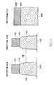
- FIG. 14Ashows an active region 200 a, gate regions 201 a, and contact regions 202 a in a standard fin-FET.
- FIG. 14Bshows thinned contact regions, i.e., an active region 200 b, gate regions 201 b, and contact regions 202 b.
- the active region 200 a shown in FIG. 14Ais shown around the active region 200 b by a broken line for comparison with FIG. 14A .
- the ON-currentcan be increased because the contact regions 202 a can be secured to be sufficiently large.
- the short channel effectcannot be suppressed sufficiently because a channel width Wa is large, i.e., larger than a gate length Lga.
- the fin-FET shown in FIG. 14Athere is proposed a method of narrowing a channel width Wb by forming the thinned active region 200 b as shown in FIG. 14B .
- a gate length Lgbis larger than the channel width Wb, so that the short channel effect can be suppressed.
- the fin-FET shown in FIG. 14Bhas the following problems. Not only the channel width Wb but also a width of each contact region 202 b is narrowed. As a result, a contact resistance is increased and ON-current is reduced accordingly.
- a semiconductor devicecomprising a fin-shaped channel region and a gate electrode, wherein the channel region located under the gate electrode has a width smaller than a gate length.
- a semiconductor devicecomprising an element isolation region formed in a semiconductor substrate; an active region surrounded by the element isolation region and elongated to a first direction; a gate electrode formed in a second direction crossing the first direction; two gate trenches formed in the semiconductor substrate located at a cross region of the active region and the gate electrode, the two gate trenches being elongated to the first direction in parallel; and a fin-shaped part that is a part of the semiconductor substrate and located between the two gate trenches, wherein the gate electrode is buried in the gate trenches and formed on the fin-shaped part, thereby the fin-shaped part serves as a channel region.
- the method of manufacturing the semiconductor device according to the present inventionincludes:
- the present inventioncan realize both suppression of the short channel effect and the increase of the ON-current for the fin field effect transistor by making the width of the channel region under the gate electrode smaller than the gate length.
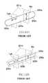
- FIGS. 1A and 1Bare plan views for explaining a semiconductor device according to an embodiment of the present invention.
- FIG. 2is a cross-sectional view showing one process (patterning of a pad oxide film 101 and a silicon nitride film 102 ) in the method of manufacturing the semiconductor device according to the embodiment of the present invention
- FIG. 3is a cross-sectional view showing one process (formation of trenches 10 t for STI) in the method of manufacturing the semiconductor device according to the embodiment of the present invention
- FIG. 4is a cross-sectional view showing one process (formation of a silicon oxide film 103 ) in the method of manufacturing the semiconductor device according to the embodiment of the present invention
- FIG. 5is a cross-sectional view showing one process (formation of an opening 104 ) in the method of manufacturing the semiconductor device according to the embodiment of the present invention
- FIG. 6is a cross-sectional view showing one process (formation of a silicon nitride film sidewall 105 ) in the method of manufacturing the semiconductor device according to the embodiment of the present invention
- FIG. 7is a plan view showing a state of FIG. 6 in the method of manufacturing a semiconductor device according to the embodiment from above;
- FIG. 8is a cross-sectional view showing one process (formation of a silicon oxide film 106 ) in the method of manufacturing the semiconductor device according to the embodiment of the present invention.
- FIG. 9is a cross-sectional view showing one process (selectively etching of the silicon nitride film 105 ) in the method of manufacturing the semiconductor device according to the embodiment of the present invention.
- FIG. 10is a cross-sectional view showing one process (formation of gate trenches 108 ) in the method of manufacturing the semiconductor device according to the embodiment of the present invention.
- FIG. 11is a cross-sectional view showing one process (formation of a sacrificial oxide film 109 ) in the method of manufacturing the semiconductor device according to the embodiment of the present invention.
- FIG. 12is a cross-sectional view showing one process (formation of a gate oxide film 110 , formation of a gate electrode 12 and formation of a source region 14 and drain region 15 ) in the method of manufacturing the semiconductor device according to the embodiment of the present invention
- FIG. 13is a cross-sectional view showing one process (selectively removing of the silicon oxide film 110 and formation of contact plugs 118 ) in the method of manufacturing the semiconductor device according to the embodiment of the present invention
- FIG. 14Ais a generally plan view of a conventional fin-FET
- FIG. 14Bis a generally plan view of a fin-FET according to a related art.
- FIG. 15is a block diagram showing a data processing system using the DRAM that the present invention is applied.
- a configuration of the memory cell transistor in the DRAM formed according to the embodiment of the present inventionwill first be described in detail.
- FIG. 1Ais a plan view showing an STI region (an element isolation region) 10 and a plurality of active regions 11 separated from one another by the STI region 10 in a memory cell region according to the embodiment. Generally, a plurality of active regions are arranged almost equally in the memory cell region. The same is true for the embodiment as shown in FIG. 1A .
- FIG. 1Bis a plan view showing one of the active regions 11 shown in FIG. 1A and the STI region 11 around the active region 11 .
- Gate trenches 12are formed in one direction to cross the active region 11 .
- a source region 14 and drain regions 15(each of which is also referred to as “contact region”) are formed in both ends of the active region 11 and between the two gate electrodes 12 .
- the source region and the drain regionare often reversed depending on whether a read-in operation or a read-out operation is performed.
- a central regionis the source region 14
- regions on both sides of the central regionare the drain regions 15
- the memory cell transistoris an N-channel transistor.
- a channel region 16 having a width W smaller than a gate length Lgis formed under each of the gate electrodes 12 .
- width W of the channel region 16By making the width W of the channel region 16 smaller than the gate length Lg, it is possible to suppress the short channel effect, to secure sufficiently large magnitudes for the contact regions 14 and 15 , and to prevent reduction in ON-current.
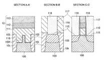
- FIGS. 2 to 6 and 8 to 13are step views schematically showing steps of manufacturing the semiconductor device according to the embodiment.
- three cross sectional views from the leftcorrespond to a section A-A′, a section B-B′, and a section C-C′ taken along a line A-A′, a line B-B′, and a line C-C′ of FIG. 1B , respectively.
- a pad oxide film 101 having a thickness of about 9 nm and a silicon nitride film 102 having a thickness of about 120 nmare formed on the semiconductor substrate 100 .
- the pad oxide film 101 and the silicon nitride film 102are dry-etched and patterned into shape corresponding to the active region 11 shown in FIGS. 1A and 1B by well-known photolithography.
- the silicon oxide film 101 and the silicon nitride film 102serve as a mask layer covering up a region to serve as the active region 11 and including opening for exposing an STI formation region.
- a surface of the semiconductor substrate 100is slightly etched as shown in the section A-A′ and the section B-B′.
- an STI trench 10 t having a depth of about 250 nmare formed in the semiconductor substrate 13 .
- an upper surface of the silicon nitride film 102is chipped by about 50 nm.
- a silicon oxide film 103 having a thickness of about 400 nmis formed on an entire surface including interior of the trench 10 t by HDP-CVD (High Density Plasma-Chemical Vapor Deposition). Thereafter, the silicon oxide film 103 is polished and removed by CMP (Chemical Mechanical Polishing) while using the silicon nitride film 102 as a stopper.
- HDP-CVDHigh Density Plasma-Chemical Vapor Deposition
- a native oxide filmis removed by wet etching.
- the silicon nitride film 102is removed by wet etching using a hot phosphoric acid at about 160° C.
- an opening 104 corresponding to the active region 11is formed on the pad oxide film 101 .
- a height from the surface of the semiconductor substrate 100 to a surface of the silicon oxide film 103is preferably equal to or smaller than 70 nm.
- etch-backis performed, thereby forming a silicon nitride film sidewall 105 on an inner side surface of the opening 104 .
- FIG. 7is a plan view showing a state of FIG. 6 from above. As shown in FIG. 7 , the silicon nitride film sidewall 105 is formed along an inner periphery of the active region 11 and an interior of the silicon nitride film sidewall 105 corresponds to the opening 104 .
- a silicon oxide film 106 having a thickness of about 100 nmis formed on the entire surface including the opening 104 surrounded by the silicon nitride film sidewall 105 (see FIG. 6 )
- the CMPis performed using the silicon nitride film side wall 105 as a stopper. By doing so, a silicon oxide film 106 is buried in the opening 104 .
- a photoresist including openings for exposing regions in which the gate electrodes 12 are to be formed(see FIG. 1B ) (that is, a photoresist patterned to open the regions in which the gate electrodes 12 are to be formed) 107 is formed, and the silicon nitride film 105 is selectively removed by dry etching.
- surfaces of the silicon oxide films 103 and 106are also etched.
- corners of the silicon oxide films 106 and 103are chipped because the corners are etched more easily.
- etching for silicon oxide filmsis performed so as to remove the pad oxide film 101 exposed between the silicon oxide films 103 and 106 .
- gate trenches 108each having a depth of about 100 nm are formed in the semiconductor substrate 100 by isotropic etching.
- an etch rate of etching the semiconductor substrate 100is preferably about 1.5 times as fast as that of etching the oxide films 103 and 106 .
- the silicon oxide films 103 and 106are also etched.
- the two trenches 108 and a fin-shaped part 100 f that is a part of the semiconductor substrate 100 held between the two gate trenches 108are formed on the semiconductor substrate 100 .
- sacrificial oxidationis performed to form a sacrificial oxide film 109 .
- the silicon nitride film 105is removed by wet etching and then the silicon oxide films 103 and 106 are wet-etched, thereby removing the surfaces of the silicon oxide films 103 and 106 , the pad oxide film 101 , and the sacrificial oxide film 109 .
- a silicon oxide film (gate oxide film) 110 having a thickness of about 6 nmis formed as a gate insulating film.
- the gate oxide film 110is formed to cover up both side surfaces and an upper surface of the fin-shaped part 100 f of the semiconductor substrate 100 .
- a doped polysilicon (DOPOS) film 111 having a thickness of about 100 nmis formed on the entire surface including interiors of the two gate trenches 108 .
- a W/WN/WSi film 112 including a stack of a tungsten silicide (WSi) film, a tungsten nitride (WN) film, and a tungsten (W) film and a having a thickness of about 70 nm, and a silicon nitride film 113 having a thickness of about 140 nmare formed on the DOPOS film 111 in this order.
- multilayer films of the DOPOS film 111 , the W/WN/WSi film 112 , and the silicon nitride film 113are patterned.
- the gate electrodes 12each having a part of an electrode material buried in the gate trenches 108 are completed.
- LDDLightly Doped Drain
- impurity ionsare implanted into the semiconductor substrate 100 , thereby forming the source and drain regions 14 and 15 .
- an interlayer insulating film 116is formed.
- contact holes 117are opened in the interlayer insulating film 116 , and contact plugs 118 are formed in the respective contact holes 117 .
- memory cell capacitors, wirings and the likeare formed by ordinary method, thus completing the DRAM.
- the width of each channel regionis made smaller than the gate length in the fin field effect transistor, whereby the short channel effect can be suppressed. Furthermore, magnitudes of the contact regions (source and drain regions) do not depend on the width of each channel region. It is, therefore, possible to secure necessary areas for the contact regions (source and drain regions) and prevent reduction in the ON-current.
- the present inventioncan preferably apply to the semiconductor memory device, especially a DRAM.
- FIG. 15is a block diagram showing a data processing system using the DRAM that the present invention is applied.
- the data processing system 300 shown in FIG. 15includes a data processor 320 and a DRAM 330 that the present invention is applied are connected to each other via a system bus 310 .
- the data processor 320can be selected from at least a microprocessor (MPU) and a digital signal processor (DSP).
- MPUmicroprocessor
- DSPdigital signal processor
- FIG. 15although the data processor 320 and the DRAM 330 are connected via the system bus 310 in order to simplify the diagram, they can be connected via not the system bus 310 but a local bus.
- FIG. 15although only one set of system bus 310 is employed in the data processing system 300 in order to simplify the diagram, a serial bus or a parallel bus connected to the system bus 310 via connectors can be provided. As shown in FIG. 15 , a storage device 340 , an I/O device 350 , and a ROM 360 are connected to the system bus 310 . However, they are not essential element for the data processing system 300 .
- the storage device 340can be selected from at least a hard disk drive, an optical disk drive, and flash memory device.
- the I/O device 350can be selected from a display device such as a liquid crystal display (LCD) and an input device such as a key board or a mouse.
- the I/O device 350can consists of either input or output device. Further, although each one element is provided as shown in FIG. 15 , two or more same elements can be provided in the data processing system.
- the present inventionis not limited to the memory but is applicable to logic-related devices.
Landscapes
- Insulated Gate Type Field-Effect Transistor (AREA)
- Semiconductor Memories (AREA)
Abstract
Description
- This application is a division of application Ser. No. 11/822,591, filed Jul. 9, 2007, now pending, and based on Japanese Patent Application No. 2006-202937, filed Jul. 26, 2006, by Hiroshi Kujirai, which is incorporated herein by reference in its entirety. This application claims only subject matter disclosed in the parent application and therefore presents no new matter.
- The present invention relates to a semiconductor device and a manufacturing method thereof, and particularly relates to a semiconductor device including a fin field effect transistor and a method of manufacturing the semiconductor method.
- In recent years, following downsizing of a memory cell in a DRAM (Dynamic Random Access Memory), a gate length of a memory cell transistor is inevitably reduced. However, if the gate length is smaller, then the short channel effect of the transistor disadvantageously becomes more conspicuous, and sub-threshold current is disadvantageously increased. Furthermore, if substrate concentration is increased to suppress the short channel effect and the increase of the sub-threshold current, junction leakage increases. Due to this, the DRAM is confronted with a serious problem of deterioration in refresh characteristics.
- As a technique for avoiding the above-stated problem, attention has been paid to a fin field effect transistor (fin-FET) structured so that channel regions are formed to be thin each in the form of a fin in a perpendicular direction to a semiconductor substrate and so that gate electrodes are arranged around each of the channel regions, as disclosed in Japanese Patent Application National Publication No. 2006-501672 and Japanese Patent Application Laid-Open No. 2005-310921. The fin-FET is expected to be able to realize acceleration of operating rate, increase in ON-current, reduction in power consumption and the like, as compared with a planer transistor.
- However, to suppress the short channel effect, it is necessary to make a channel width smaller than a gate length in the fin-FET.
FIG. 14A is a generally plan view of a conventional fin-FET.FIG. 14B is a generally plan view of a fin-FET according to a related art.FIG. 14A shows anactive region 200a,gate regions 201a,andcontact regions 202ain a standard fin-FET.FIG. 14B shows thinned contact regions, i.e., anactive region 200b,gate regions 201b,andcontact regions 202b.InFIG. 14B , theactive region 200ashown inFIG. 14A is shown around theactive region 200bby a broken line for comparison withFIG. 14A .- In
FIG. 14A , the ON-current can be increased because thecontact regions 202acan be secured to be sufficiently large. However, the short channel effect cannot be suppressed sufficiently because a channel width Wa is large, i.e., larger than a gate length Lga. - To solve the problem of the conventional fin-FET shown in
FIG. 14A , there is proposed a method of narrowing a channel width Wb by forming the thinnedactive region 200bas shown inFIG. 14B . By doing so, a gate length Lgb is larger than the channel width Wb, so that the short channel effect can be suppressed. However, the fin-FET shown inFIG. 14B has the following problems. Not only the channel width Wb but also a width of eachcontact region 202bis narrowed. As a result, a contact resistance is increased and ON-current is reduced accordingly. - Therefore, it is an object of the present invention to provide a semiconductor device and a semiconductor device manufacturing method capable of suppressing the short channel effect and increasing ON-current.
- According to the present invention, there is provided a semiconductor device comprising a fin-shaped channel region and a gate electrode, wherein the channel region located under the gate electrode has a width smaller than a gate length.
- According to the present invention, there is provided a semiconductor device comprising an element isolation region formed in a semiconductor substrate; an active region surrounded by the element isolation region and elongated to a first direction; a gate electrode formed in a second direction crossing the first direction; two gate trenches formed in the semiconductor substrate located at a cross region of the active region and the gate electrode, the two gate trenches being elongated to the first direction in parallel; and a fin-shaped part that is a part of the semiconductor substrate and located between the two gate trenches, wherein the gate electrode is buried in the gate trenches and formed on the fin-shaped part, thereby the fin-shaped part serves as a channel region.
- Moreover, the method of manufacturing the semiconductor device according to the present invention includes:
- forming a mask layer on a semiconductor substrate, the mask layer covering up a region to serve as an active region and including an opening for exposing a region to serve as an STI region;
- forming a trench for the STI region using the mask layer;
- forming a first insulating film in the trench and in the opening of the mask layer without removing the mask layer;
- forming a second opening corresponding to the mask layer in the first insulating film by selectively removing the mask layer;
- forming a sidewall insulating film on an inner wall of the second opening;
- forming a second insulating film in the second opening in which the sidewall insulating film is formed;
- selectively removing the sidewall insulating film in a region in which a gate electrode is to be formed;
- forming two trenches in the region in which the gate electrode is to be formed on the semiconductor substrate using the first insulating film and the second insulating film as a mask, and forming a fin-shaped part which is located between the two gate trenches, which is a part of the semiconductor substrate, and which is to serve as a channel region;
- forming a gate insulating film at least on an upper surface and a side surface of the fin-shaped part; and
- forming the gate electrode buried in the two gate trenches and covering up the fin-shaped part. With such a method, the width of the channel region under the gate electrode can be made smaller than the gate length.
- As described above, the present invention can realize both suppression of the short channel effect and the increase of the ON-current for the fin field effect transistor by making the width of the channel region under the gate electrode smaller than the gate length.
- The above and other objects, features and advantages of this invention will become more apparent by reference to the following detailed description of the invention taken in conjunction with the accompanying drawings, wherein:
FIGS. 1A and 1B are plan views for explaining a semiconductor device according to an embodiment of the present invention;FIG. 2 is a cross-sectional view showing one process (patterning of apad oxide film 101 and a silicon nitride film102) in the method of manufacturing the semiconductor device according to the embodiment of the present invention;FIG. 3 is a cross-sectional view showing one process (formation oftrenches 10tfor STI) in the method of manufacturing the semiconductor device according to the embodiment of the present invention;FIG. 4 is a cross-sectional view showing one process (formation of a silicon oxide film103) in the method of manufacturing the semiconductor device according to the embodiment of the present invention;FIG. 5 is a cross-sectional view showing one process (formation of an opening104) in the method of manufacturing the semiconductor device according to the embodiment of the present invention;FIG. 6 is a cross-sectional view showing one process (formation of a silicon nitride film sidewall105) in the method of manufacturing the semiconductor device according to the embodiment of the present invention;FIG. 7 is a plan view showing a state ofFIG. 6 in the method of manufacturing a semiconductor device according to the embodiment from above;FIG. 8 is a cross-sectional view showing one process (formation of a silicon oxide film106) in the method of manufacturing the semiconductor device according to the embodiment of the present invention;FIG. 9 is a cross-sectional view showing one process (selectively etching of the silicon nitride film105) in the method of manufacturing the semiconductor device according to the embodiment of the present invention;FIG. 10 is a cross-sectional view showing one process (formation of gate trenches108) in the method of manufacturing the semiconductor device according to the embodiment of the present invention;FIG. 11 is a cross-sectional view showing one process (formation of a sacrificial oxide film109) in the method of manufacturing the semiconductor device according to the embodiment of the present invention;FIG. 12 is a cross-sectional view showing one process (formation of agate oxide film 110, formation of agate electrode 12 and formation of asource region 14 and drain region15) in the method of manufacturing the semiconductor device according to the embodiment of the present invention;FIG. 13 is a cross-sectional view showing one process (selectively removing of thesilicon oxide film 110 and formation of contact plugs118) in the method of manufacturing the semiconductor device according to the embodiment of the present invention;FIG. 14A is a generally plan view of a conventional fin-FET andFIG. 14B is a generally plan view of a fin-FET according to a related art; andFIG. 15 is a block diagram showing a data processing system using the DRAM that the present invention is applied.- Preferred embodiments of the present invention will be explained below with reference to the accompanying drawings.
- Note that the following embodiment is an example of applying the present invention to a memory cell transistor in a DRAM.
- A configuration of the memory cell transistor in the DRAM formed according to the embodiment of the present invention will first be described in detail.
FIG. 1A is a plan view showing an STI region (an element isolation region)10 and a plurality ofactive regions 11 separated from one another by theSTI region 10 in a memory cell region according to the embodiment. Generally, a plurality of active regions are arranged almost equally in the memory cell region. The same is true for the embodiment as shown inFIG. 1A .FIG. 1B is a plan view showing one of theactive regions 11 shown inFIG. 1A and theSTI region 11 around theactive region 11.Gate trenches 12 are formed in one direction to cross theactive region 11. Asource region 14 and drain regions15 (each of which is also referred to as “contact region”) are formed in both ends of theactive region 11 and between the twogate electrodes 12. In the embodiment, because the present invention is applied to the memory cell transistor in the DRAM, the source region and the drain region are often reversed depending on whether a read-in operation or a read-out operation is performed. In the embodiment, it is assumed that a central region is thesource region 14, regions on both sides of the central region are thedrain regions 15, and that the memory cell transistor is an N-channel transistor.- As shown in
FIG. 1B , achannel region 16 having a width W smaller than a gate length Lg is formed under each of thegate electrodes 12. - By making the width W of the
channel region 16 smaller than the gate length Lg, it is possible to suppress the short channel effect, to secure sufficiently large magnitudes for thecontact regions - A method of manufacturing a semiconductor device according to the embodiment of the present invention will next be described in detail with reference to
FIGS. 2 to 13 .FIGS. 2 to 6 and8 to13 are step views schematically showing steps of manufacturing the semiconductor device according to the embodiment. In each ofFIGS. 2 to 6 and8 to13, three cross sectional views from the left correspond to a section A-A′, a section B-B′, and a section C-C′ taken along a line A-A′, a line B-B′, and a line C-C′ ofFIG. 1B , respectively. - As shown in
FIG. 2 , apad oxide film 101 having a thickness of about 9 nm and asilicon nitride film 102 having a thickness of about 120 nm are formed on thesemiconductor substrate 100. Thepad oxide film 101 and thesilicon nitride film 102 are dry-etched and patterned into shape corresponding to theactive region 11 shown inFIGS. 1A and 1B by well-known photolithography. As a result, thesilicon oxide film 101 and thesilicon nitride film 102 serve as a mask layer covering up a region to serve as theactive region 11 and including opening for exposing an STI formation region. At this time, because over-etching is performed, a surface of thesemiconductor substrate 100 is slightly etched as shown in the section A-A′ and the section B-B′. - As shown in
FIG. 3 , while using thesilicon nitride film 102 as a mask, anSTI trench 10thaving a depth of about 250 nm are formed in the semiconductor substrate13. At this time, an upper surface of thesilicon nitride film 102 is chipped by about 50 nm. - As shown in
FIG. 4 , asilicon oxide film 103 having a thickness of about 400 nm is formed on an entire surface including interior of thetrench 10tby HDP-CVD (High Density Plasma-Chemical Vapor Deposition). Thereafter, thesilicon oxide film 103 is polished and removed by CMP (Chemical Mechanical Polishing) while using thesilicon nitride film 102 as a stopper. - After the CMP, a native oxide film is removed by wet etching. Next, as shown in
FIG. 5 , thesilicon nitride film 102 is removed by wet etching using a hot phosphoric acid at about 160° C. As a result, anopening 104 corresponding to theactive region 11 is formed on thepad oxide film 101. At this time, a height from the surface of thesemiconductor substrate 100 to a surface of thesilicon oxide film 103 is preferably equal to or smaller than 70 nm. - As shown in
FIG. 6 , after asilicon nitride film 105 having a thickness of about 20 nm to 35 nm is formed on the entire surface, etch-back is performed, thereby forming a siliconnitride film sidewall 105 on an inner side surface of theopening 104. FIG. 7 is a plan view showing a state ofFIG. 6 from above. As shown inFIG. 7 , the siliconnitride film sidewall 105 is formed along an inner periphery of theactive region 11 and an interior of the siliconnitride film sidewall 105 corresponds to theopening 104.- Next, as shown in
FIG. 8 , after asilicon oxide film 106 having a thickness of about 100 nm is formed on the entire surface including theopening 104 surrounded by the silicon nitride film sidewall105 (seeFIG. 6 ), the CMP is performed using the silicon nitridefilm side wall 105 as a stopper. By doing so, asilicon oxide film 106 is buried in theopening 104. - As shown in
FIG. 9 , a photoresist including openings for exposing regions in which thegate electrodes 12 are to be formed (seeFIG. 1B ) (that is, a photoresist patterned to open the regions in which thegate electrodes 12 are to be formed)107 is formed, and thesilicon nitride film 105 is selectively removed by dry etching. At this time, surfaces of thesilicon oxide films silicon oxide films - After removing the
photoresist 107, etching for silicon oxide films is performed so as to remove thepad oxide film 101 exposed between thesilicon oxide films - As shown in
FIG. 10 , while using thesilicon oxide films gate trenches 108 each having a depth of about 100 nm are formed in thesemiconductor substrate 100 by isotropic etching. At this time, an etch rate of etching thesemiconductor substrate 100 is preferably about 1.5 times as fast as that of etching theoxide films silicon oxide films - In this manner, the two
trenches 108 and a fin-shapedpart 100fthat is a part of thesemiconductor substrate 100 held between the twogate trenches 108 are formed on thesemiconductor substrate 100. - As shown in
FIG. 11 , sacrificial oxidation is performed to form asacrificial oxide film 109. - Thereafter, the
silicon nitride film 105 is removed by wet etching and then thesilicon oxide films silicon oxide films pad oxide film 101, and thesacrificial oxide film 109. - As shown in
FIG. 12 , a silicon oxide film (gate oxide film)110 having a thickness of about 6 nm is formed as a gate insulating film. Thegate oxide film 110 is formed to cover up both side surfaces and an upper surface of the fin-shapedpart 100fof thesemiconductor substrate 100. - Next, a doped polysilicon (DOPOS)
film 111 having a thickness of about 100 nm is formed on the entire surface including interiors of the twogate trenches 108. A W/WN/WSi film 112 including a stack of a tungsten silicide (WSi) film, a tungsten nitride (WN) film, and a tungsten (W) film and a having a thickness of about 70 nm, and asilicon nitride film 113 having a thickness of about 140 nm are formed on theDOPOS film 111 in this order. Thereafter, multilayer films of theDOPOS film 111, the W/WN/WSi film 112, and thesilicon nitride film 113 are patterned. As a result, thegate electrodes 12 each having a part of an electrode material buried in thegate trenches 108 are completed. - Next, while the
gate electrodes 12 are used as a mask, impurity ions are implanted into thesemiconductor substrate 100 to form an LDD (Lightly Doped Drain) layer. Thereafter, sidewall insulatingfilms 114 each having a thickness of 25 nm to 35 nm is formed on respective side surfaces of thegate electrodes 12. - While using the
gate electrodes 12 and thesidewall insulating films 114 as a mask, impurity ions are implanted into thesemiconductor substrate 100, thereby forming the source and drainregions - Thereafter, as shown in
FIG. 13 , after thegate oxide film 110 on the source and drainregions contact regions 115, aninterlayer insulating film 116 is formed. Next, contact holes117 are opened in theinterlayer insulating film 116, and contact plugs118 are formed in the respective contact holes117. - Thereafter, although not shown in the drawings, memory cell capacitors, wirings and the like are formed by ordinary method, thus completing the DRAM.
- As described above, according to the embodiment of the present invention, the width of each channel region is made smaller than the gate length in the fin field effect transistor, whereby the short channel effect can be suppressed. Furthermore, magnitudes of the contact regions (source and drain regions) do not depend on the width of each channel region. It is, therefore, possible to secure necessary areas for the contact regions (source and drain regions) and prevent reduction in the ON-current.
- The present invention can preferably apply to the semiconductor memory device, especially a DRAM.
FIG. 15 is a block diagram showing a data processing system using the DRAM that the present invention is applied.- The
data processing system 300 shown inFIG. 15 includes adata processor 320 and aDRAM 330 that the present invention is applied are connected to each other via asystem bus 310. Thedata processor 320 can be selected from at least a microprocessor (MPU) and a digital signal processor (DSP). InFIG. 15 , although thedata processor 320 and theDRAM 330 are connected via thesystem bus 310 in order to simplify the diagram, they can be connected via not thesystem bus 310 but a local bus. - Further, in
FIG. 15 , although only one set ofsystem bus 310 is employed in thedata processing system 300 in order to simplify the diagram, a serial bus or a parallel bus connected to thesystem bus 310 via connectors can be provided. As shown inFIG. 15 , astorage device 340, an I/O device 350, and aROM 360 are connected to thesystem bus 310. However, they are not essential element for thedata processing system 300. - The
storage device 340 can be selected from at least a hard disk drive, an optical disk drive, and flash memory device. The I/O device 350 can be selected from a display device such as a liquid crystal display (LCD) and an input device such as a key board or a mouse. The I/O device 350 can consists of either input or output device. Further, although each one element is provided as shown inFIG. 15 , two or more same elements can be provided in the data processing system. - While a preferred embodiment of the present invention has been described hereinbefore, the present invention is not limited to the aforementioned embodiment and various modifications can be made without departing from the spirit of the present invention. It goes without saying that such modifications are included in the scope of the present invention.
- For example, while the example of applying the present invention to the memory cell transistor in the DRAM has been described in the embodiment, the present invention is not limited to the memory but is applicable to logic-related devices.
Claims (10)
Priority Applications (1)
| Application Number | Priority Date | Filing Date | Title |
|---|---|---|---|
| US12/822,862US7867856B2 (en) | 2006-07-26 | 2010-06-24 | Method of manufacturing a semiconductor device having fin-field effect transistor |
Applications Claiming Priority (4)
| Application Number | Priority Date | Filing Date | Title |
|---|---|---|---|
| JP2006202937AJP4552908B2 (en) | 2006-07-26 | 2006-07-26 | Manufacturing method of semiconductor device |
| JP2006-202937 | 2006-07-26 | ||
| US11/822,591US20080023757A1 (en) | 2006-07-26 | 2007-07-09 | Semiconductor device having fin-field effect transistor and manufacturing method thereof |
| US12/822,862US7867856B2 (en) | 2006-07-26 | 2010-06-24 | Method of manufacturing a semiconductor device having fin-field effect transistor |
Related Parent Applications (1)
| Application Number | Title | Priority Date | Filing Date |
|---|---|---|---|
| US11/822,591DivisionUS20080023757A1 (en) | 2006-07-26 | 2007-07-09 | Semiconductor device having fin-field effect transistor and manufacturing method thereof |
Publications (2)
| Publication Number | Publication Date |
|---|---|
| US20100261328A1true US20100261328A1 (en) | 2010-10-14 |
| US7867856B2 US7867856B2 (en) | 2011-01-11 |
Family
ID=38985307
Family Applications (2)
| Application Number | Title | Priority Date | Filing Date |
|---|---|---|---|
| US11/822,591AbandonedUS20080023757A1 (en) | 2006-07-26 | 2007-07-09 | Semiconductor device having fin-field effect transistor and manufacturing method thereof |
| US12/822,862ActiveUS7867856B2 (en) | 2006-07-26 | 2010-06-24 | Method of manufacturing a semiconductor device having fin-field effect transistor |
Family Applications Before (1)
| Application Number | Title | Priority Date | Filing Date |
|---|---|---|---|
| US11/822,591AbandonedUS20080023757A1 (en) | 2006-07-26 | 2007-07-09 | Semiconductor device having fin-field effect transistor and manufacturing method thereof |
Country Status (2)
| Country | Link |
|---|---|
| US (2) | US20080023757A1 (en) |
| JP (1) | JP4552908B2 (en) |
Cited By (5)
| Publication number | Priority date | Publication date | Assignee | Title |
|---|---|---|---|---|
| US8860104B2 (en) | 2011-09-06 | 2014-10-14 | Kabushiki Kaisha Toshiba | Semiconductor device and method for manufacturing same |
| US20160163837A1 (en)* | 2014-09-18 | 2016-06-09 | United Microelectronics Corporation | Fin field effect transistor device and fabrication method thereof |
| US9466669B2 (en) | 2014-05-05 | 2016-10-11 | Samsung Electronics Co., Ltd. | Multiple channel length finFETs with same physical gate length |
| US10559690B2 (en) | 2014-09-18 | 2020-02-11 | International Business Machines Corporation | Embedded source/drain structure for tall FinFET and method of formation |
| US11075286B2 (en)* | 2016-12-12 | 2021-07-27 | Intel Corporation | Hybrid finfet structure with bulk source/drain regions |
Families Citing this family (5)
| Publication number | Priority date | Publication date | Assignee | Title |
|---|---|---|---|---|
| US8866254B2 (en) | 2008-02-19 | 2014-10-21 | Micron Technology, Inc. | Devices including fin transistors robust to gate shorts and methods of making the same |
| JP5166458B2 (en)* | 2010-01-22 | 2013-03-21 | 株式会社東芝 | Semiconductor device and manufacturing method thereof |
| US9490176B2 (en) | 2014-10-17 | 2016-11-08 | Taiwan Semiconductor Manufacturing Company, Ltd. | Method and structure for FinFET isolation |
| KR102605621B1 (en) | 2019-01-25 | 2023-11-23 | 삼성전자주식회사 | Method for manufacturing semiconductor device having buried gate electrodes |
| US11502163B2 (en)* | 2019-10-23 | 2022-11-15 | Nanya Technology Corporation | Semiconductor structure and fabrication method thereof |
Citations (14)
| Publication number | Priority date | Publication date | Assignee | Title |
|---|---|---|---|---|
| US6222225B1 (en)* | 1998-09-29 | 2001-04-24 | Kabushiki Kaisha Toshiba | Semiconductor device and manufacturing method thereof |
| US20020011612A1 (en)* | 2000-07-31 | 2002-01-31 | Kabushiki Kaisha Toshiba | Semiconductor device and method for manufacturing the same |
| US6764884B1 (en)* | 2003-04-03 | 2004-07-20 | Advanced Micro Devices, Inc. | Method for forming a gate in a FinFET device and thinning a fin in a channel region of the FinFET device |
| US6800910B2 (en)* | 2002-09-30 | 2004-10-05 | Advanced Micro Devices, Inc. | FinFET device incorporating strained silicon in the channel region |
| US20050051825A1 (en)* | 2003-09-09 | 2005-03-10 | Makoto Fujiwara | Semiconductor device and manufacturing method thereof |
| US20050136617A1 (en)* | 2003-12-03 | 2005-06-23 | Young-Chul Jang | MOS transistor having protruded-shape channel and method of fabricating the same |
| US20050186742A1 (en)* | 2004-02-24 | 2005-08-25 | Chang-Woo Oh | Vertical channel fin field-effect transistors having increased source/drain contact area and methods for fabricating the same |
| US20050224800A1 (en)* | 2004-03-31 | 2005-10-13 | Nick Lindert | Bulk non-planar transistor having strained enhanced mobility and methods of fabrication |
| US6967175B1 (en)* | 2003-12-04 | 2005-11-22 | Advanced Micro Devices, Inc. | Damascene gate semiconductor processing with local thinning of channel region |
| US20050272195A1 (en)* | 2003-07-01 | 2005-12-08 | Andres Bryant | Integrated circuit having pairs of parallel complementary finfets |
| US20050285186A1 (en)* | 2004-06-29 | 2005-12-29 | Kabushiki Kaisha Toshiba | Semiconductor device and method of fabricating the same |
| US20060054969A1 (en)* | 2004-09-10 | 2006-03-16 | Se-Myeong Jang | Semiconductor device having a junction extended by a selective epitaxial growth (SEG) layer and method of fabricating the same |
| US7323375B2 (en)* | 2004-05-04 | 2008-01-29 | Samsung Electronics Co., Ltd. | Fin field effect transistor device and method of fabricating the same |
| US7453124B2 (en)* | 2004-06-22 | 2008-11-18 | Sharp Kabushiki Kaisha | Field effect transistor and fabrication method thereof |
Family Cites Families (10)
| Publication number | Priority date | Publication date | Assignee | Title |
|---|---|---|---|---|
| JPS5710973A (en)* | 1980-06-24 | 1982-01-20 | Agency Of Ind Science & Technol | Semiconductor device |
| JPH07131009A (en)* | 1993-11-04 | 1995-05-19 | Toshiba Corp | Semiconductor device and manufacturing method thereof |
| JPH08181323A (en)* | 1994-12-27 | 1996-07-12 | Hitachi Ltd | Semiconductor device and manufacturing method thereof |
| JP2002151688A (en)* | 2000-08-28 | 2002-05-24 | Mitsubishi Electric Corp | MOS type semiconductor device and method of manufacturing the same |
| JP4870291B2 (en)* | 2001-09-26 | 2012-02-08 | シャープ株式会社 | Semiconductor device, manufacturing method thereof, integrated circuit, and semiconductor system |
| US6818952B2 (en)* | 2002-10-01 | 2004-11-16 | International Business Machines Corporation | Damascene gate multi-mesa MOSFET |
| KR100769418B1 (en)* | 2003-03-20 | 2007-10-22 | 마츠시타 덴끼 산교 가부시키가이샤 | Finfet-type semiconductor device and method for fabricating the same |
| JP2005310921A (en) | 2004-04-19 | 2005-11-04 | Okayama Prefecture | MOS type semiconductor device and manufacturing method thereof |
| JPWO2006006438A1 (en)* | 2004-07-12 | 2008-04-24 | 日本電気株式会社 | Semiconductor device and manufacturing method thereof |
| US7678648B2 (en)* | 2006-07-14 | 2010-03-16 | Micron Technology, Inc. | Subresolution silicon features and methods for forming the same |
- 2006
- 2006-07-26JPJP2006202937Apatent/JP4552908B2/enactiveActive
- 2007
- 2007-07-09USUS11/822,591patent/US20080023757A1/ennot_activeAbandoned
- 2010
- 2010-06-24USUS12/822,862patent/US7867856B2/enactiveActive
Patent Citations (15)
| Publication number | Priority date | Publication date | Assignee | Title |
|---|---|---|---|---|
| US6222225B1 (en)* | 1998-09-29 | 2001-04-24 | Kabushiki Kaisha Toshiba | Semiconductor device and manufacturing method thereof |
| US20020011612A1 (en)* | 2000-07-31 | 2002-01-31 | Kabushiki Kaisha Toshiba | Semiconductor device and method for manufacturing the same |
| US6800910B2 (en)* | 2002-09-30 | 2004-10-05 | Advanced Micro Devices, Inc. | FinFET device incorporating strained silicon in the channel region |
| US6764884B1 (en)* | 2003-04-03 | 2004-07-20 | Advanced Micro Devices, Inc. | Method for forming a gate in a FinFET device and thinning a fin in a channel region of the FinFET device |
| US20050272195A1 (en)* | 2003-07-01 | 2005-12-08 | Andres Bryant | Integrated circuit having pairs of parallel complementary finfets |
| US20050051825A1 (en)* | 2003-09-09 | 2005-03-10 | Makoto Fujiwara | Semiconductor device and manufacturing method thereof |
| US7129550B2 (en)* | 2003-09-09 | 2006-10-31 | Kabushiki Kaisha Toshiba | Fin-shaped semiconductor device |
| US20050136617A1 (en)* | 2003-12-03 | 2005-06-23 | Young-Chul Jang | MOS transistor having protruded-shape channel and method of fabricating the same |
| US6967175B1 (en)* | 2003-12-04 | 2005-11-22 | Advanced Micro Devices, Inc. | Damascene gate semiconductor processing with local thinning of channel region |
| US20050186742A1 (en)* | 2004-02-24 | 2005-08-25 | Chang-Woo Oh | Vertical channel fin field-effect transistors having increased source/drain contact area and methods for fabricating the same |
| US20050224800A1 (en)* | 2004-03-31 | 2005-10-13 | Nick Lindert | Bulk non-planar transistor having strained enhanced mobility and methods of fabrication |
| US7323375B2 (en)* | 2004-05-04 | 2008-01-29 | Samsung Electronics Co., Ltd. | Fin field effect transistor device and method of fabricating the same |
| US7453124B2 (en)* | 2004-06-22 | 2008-11-18 | Sharp Kabushiki Kaisha | Field effect transistor and fabrication method thereof |
| US20050285186A1 (en)* | 2004-06-29 | 2005-12-29 | Kabushiki Kaisha Toshiba | Semiconductor device and method of fabricating the same |
| US20060054969A1 (en)* | 2004-09-10 | 2006-03-16 | Se-Myeong Jang | Semiconductor device having a junction extended by a selective epitaxial growth (SEG) layer and method of fabricating the same |
Cited By (7)
| Publication number | Priority date | Publication date | Assignee | Title |
|---|---|---|---|---|
| US8860104B2 (en) | 2011-09-06 | 2014-10-14 | Kabushiki Kaisha Toshiba | Semiconductor device and method for manufacturing same |
| US9466669B2 (en) | 2014-05-05 | 2016-10-11 | Samsung Electronics Co., Ltd. | Multiple channel length finFETs with same physical gate length |
| US20160163837A1 (en)* | 2014-09-18 | 2016-06-09 | United Microelectronics Corporation | Fin field effect transistor device and fabrication method thereof |
| US9634125B2 (en)* | 2014-09-18 | 2017-04-25 | United Microelectronics Corporation | Fin field effect transistor device and fabrication method thereof |
| US10559690B2 (en) | 2014-09-18 | 2020-02-11 | International Business Machines Corporation | Embedded source/drain structure for tall FinFET and method of formation |
| US10896976B2 (en) | 2014-09-18 | 2021-01-19 | International Business Machines Corporation | Embedded source/drain structure for tall FinFet and method of formation |
| US11075286B2 (en)* | 2016-12-12 | 2021-07-27 | Intel Corporation | Hybrid finfet structure with bulk source/drain regions |
Also Published As
| Publication number | Publication date |
|---|---|
| US20080023757A1 (en) | 2008-01-31 |
| JP4552908B2 (en) | 2010-09-29 |
| US7867856B2 (en) | 2011-01-11 |
| JP2008034427A (en) | 2008-02-14 |
Similar Documents
| Publication | Publication Date | Title |
|---|---|---|
| US7867856B2 (en) | Method of manufacturing a semiconductor device having fin-field effect transistor | |
| KR100739653B1 (en) | Fin field effect transistor and its manufacturing method | |
| US8116121B2 (en) | Semiconductor device and manufacturing methods with using non-planar type of transistors | |
| US20060071299A1 (en) | Independently accessed double-gate and tri-gate transistors in same process flow | |
| US20080299734A1 (en) | Method of manufacturing a self-aligned fin field effect transistor (FinFET) device | |
| JP5718585B2 (en) | Semiconductor device, manufacturing method thereof, and data processing system | |
| US7923773B2 (en) | Semiconductor device, manufacturing method thereof, and data processing system | |
| US6872629B2 (en) | Method of forming a memory cell with a single sided buried strap | |
| US7645671B2 (en) | Recessed access device for a memory | |
| US20080318388A1 (en) | Method for fabricating mos transistor with recess channel | |
| JP2007158269A (en) | Semiconductor device and manufacturing method thereof | |
| JP2009158813A (en) | Semiconductor device manufacturing method and semiconductor device | |
| JP4600834B2 (en) | Manufacturing method of semiconductor device | |
| US20070224756A1 (en) | Method for fabricating recessed gate mos transistor device | |
| US7692251B2 (en) | Transistor for semiconductor device and method of forming the same | |
| JP4470188B2 (en) | Manufacturing method of semiconductor device | |
| JP2016046414A (en) | Method of manufacturing semiconductor device | |
| US20060019447A1 (en) | Process for the self-aligning production of a transistor with a U-shaped gate | |
| JP5307971B2 (en) | Manufacturing method of semiconductor device | |
| JP2008016636A (en) | Semiconductor device and manufacturing method thereof | |
| JP2011029509A (en) | Semiconductor device and method of manufacturing the same | |
| US7214980B2 (en) | Semiconductor device with a self-aligned contact (SAC) structure | |
| KR20110079279A (en) | Semiconductor device and manufacturing method | |
| JP2013110256A (en) | Semiconductor device manufacturing method | |
| JP2007013195A (en) | Method of manufacturing semiconductor integrated circuit device |
Legal Events
| Date | Code | Title | Description |
|---|---|---|---|
| STCF | Information on status: patent grant | Free format text:PATENTED CASE | |
| FEPP | Fee payment procedure | Free format text:PAYOR NUMBER ASSIGNED (ORIGINAL EVENT CODE: ASPN); ENTITY STATUS OF PATENT OWNER: LARGE ENTITY | |
| AS | Assignment | Owner name:MICRON TECHNOLOGY, INC., IDAHO Free format text:ASSIGNMENT OF ASSIGNORS INTEREST;ASSIGNOR:ELPIDA MEMORY, INC.;REEL/FRAME:032645/0422 Effective date:20140220 | |
| FPAY | Fee payment | Year of fee payment:4 | |
| AS | Assignment | Owner name:U.S. BANK NATIONAL ASSOCIATION, AS COLLATERAL AGENT, CALIFORNIA Free format text:SECURITY INTEREST;ASSIGNOR:MICRON TECHNOLOGY, INC.;REEL/FRAME:038669/0001 Effective date:20160426 Owner name:U.S. BANK NATIONAL ASSOCIATION, AS COLLATERAL AGEN Free format text:SECURITY INTEREST;ASSIGNOR:MICRON TECHNOLOGY, INC.;REEL/FRAME:038669/0001 Effective date:20160426 | |
| AS | Assignment | Owner name:MORGAN STANLEY SENIOR FUNDING, INC., AS COLLATERAL AGENT, MARYLAND Free format text:PATENT SECURITY AGREEMENT;ASSIGNOR:MICRON TECHNOLOGY, INC.;REEL/FRAME:038954/0001 Effective date:20160426 Owner name:MORGAN STANLEY SENIOR FUNDING, INC., AS COLLATERAL Free format text:PATENT SECURITY AGREEMENT;ASSIGNOR:MICRON TECHNOLOGY, INC.;REEL/FRAME:038954/0001 Effective date:20160426 | |
| AS | Assignment | Owner name:U.S. BANK NATIONAL ASSOCIATION, AS COLLATERAL AGENT, CALIFORNIA Free format text:CORRECTIVE ASSIGNMENT TO CORRECT THE REPLACE ERRONEOUSLY FILED PATENT #7358718 WITH THE CORRECT PATENT #7358178 PREVIOUSLY RECORDED ON REEL 038669 FRAME 0001. ASSIGNOR(S) HEREBY CONFIRMS THE SECURITY INTEREST;ASSIGNOR:MICRON TECHNOLOGY, INC.;REEL/FRAME:043079/0001 Effective date:20160426 Owner name:U.S. BANK NATIONAL ASSOCIATION, AS COLLATERAL AGEN Free format text:CORRECTIVE ASSIGNMENT TO CORRECT THE REPLACE ERRONEOUSLY FILED PATENT #7358718 WITH THE CORRECT PATENT #7358178 PREVIOUSLY RECORDED ON REEL 038669 FRAME 0001. ASSIGNOR(S) HEREBY CONFIRMS THE SECURITY INTEREST;ASSIGNOR:MICRON TECHNOLOGY, INC.;REEL/FRAME:043079/0001 Effective date:20160426 | |
| MAFP | Maintenance fee payment | Free format text:PAYMENT OF MAINTENANCE FEE, 8TH YEAR, LARGE ENTITY (ORIGINAL EVENT CODE: M1552) Year of fee payment:8 | |
| AS | Assignment | Owner name:JPMORGAN CHASE BANK, N.A., AS COLLATERAL AGENT, ILLINOIS Free format text:SECURITY INTEREST;ASSIGNORS:MICRON TECHNOLOGY, INC.;MICRON SEMICONDUCTOR PRODUCTS, INC.;REEL/FRAME:047540/0001 Effective date:20180703 Owner name:JPMORGAN CHASE BANK, N.A., AS COLLATERAL AGENT, IL Free format text:SECURITY INTEREST;ASSIGNORS:MICRON TECHNOLOGY, INC.;MICRON SEMICONDUCTOR PRODUCTS, INC.;REEL/FRAME:047540/0001 Effective date:20180703 | |
| AS | Assignment | Owner name:MICRON TECHNOLOGY, INC., IDAHO Free format text:RELEASE BY SECURED PARTY;ASSIGNOR:U.S. BANK NATIONAL ASSOCIATION, AS COLLATERAL AGENT;REEL/FRAME:047243/0001 Effective date:20180629 | |
| AS | Assignment | Owner name:MICRON TECHNOLOGY, INC., IDAHO Free format text:RELEASE BY SECURED PARTY;ASSIGNOR:MORGAN STANLEY SENIOR FUNDING, INC., AS COLLATERAL AGENT;REEL/FRAME:050937/0001 Effective date:20190731 | |
| AS | Assignment | Owner name:MICRON SEMICONDUCTOR PRODUCTS, INC., IDAHO Free format text:RELEASE BY SECURED PARTY;ASSIGNOR:JPMORGAN CHASE BANK, N.A., AS COLLATERAL AGENT;REEL/FRAME:051028/0001 Effective date:20190731 Owner name:MICRON TECHNOLOGY, INC., IDAHO Free format text:RELEASE BY SECURED PARTY;ASSIGNOR:JPMORGAN CHASE BANK, N.A., AS COLLATERAL AGENT;REEL/FRAME:051028/0001 Effective date:20190731 | |
| MAFP | Maintenance fee payment | Free format text:PAYMENT OF MAINTENANCE FEE, 12TH YEAR, LARGE ENTITY (ORIGINAL EVENT CODE: M1553); ENTITY STATUS OF PATENT OWNER: LARGE ENTITY Year of fee payment:12 |