US20100261307A1 - Patterning electrode materials free from berm structures for thin film photovoltaic cells - Google Patents
Patterning electrode materials free from berm structures for thin film photovoltaic cellsDownload PDFInfo
- Publication number
- US20100261307A1 US20100261307A1US12/565,735US56573509AUS2010261307A1US 20100261307 A1US20100261307 A1US 20100261307A1US 56573509 AUS56573509 AUS 56573509AUS 2010261307 A1US2010261307 A1US 2010261307A1
- Authority
- US
- United States
- Prior art keywords
- electrode layer
- lower electrode
- layer
- patterns
- forming
- Prior art date
- Legal status (The legal status is an assumption and is not a legal conclusion. Google has not performed a legal analysis and makes no representation as to the accuracy of the status listed.)
- Granted
Links
- 239000010409thin filmSubstances0.000titleclaimsabstractdescription52
- 238000000059patterningMethods0.000titledescription9
- 239000007772electrode materialSubstances0.000titledescription6
- 238000000034methodMethods0.000claimsabstractdescription139
- 239000000463materialSubstances0.000claimsabstractdescription75
- XLOMVQKBTHCTTD-UHFFFAOYSA-NZinc monoxideChemical compound[Zn]=OXLOMVQKBTHCTTD-UHFFFAOYSA-N0.000claimsabstractdescription51
- 239000000758substrateSubstances0.000claimsabstractdescription48
- 239000005361soda-lime glassSubstances0.000claimsabstractdescription30
- 239000011787zinc oxideSubstances0.000claimsabstractdescription25
- 230000005670electromagnetic radiationEffects0.000claimsabstractdescription12
- 238000012545processingMethods0.000claimsabstractdescription12
- ZOKXTWBITQBERF-UHFFFAOYSA-NMolybdenumChemical compound[Mo]ZOKXTWBITQBERF-UHFFFAOYSA-N0.000claimsabstractdescription10
- 239000010408filmSubstances0.000claimsabstractdescription10
- 229910052750molybdenumInorganic materials0.000claimsabstractdescription10
- 239000011733molybdenumSubstances0.000claimsabstractdescription10
- 239000007788liquidSubstances0.000claimsdescription23
- 238000004140cleaningMethods0.000claimsdescription20
- 230000004888barrier functionEffects0.000claimsdescription18
- KTSFMFGEAAANTF-UHFFFAOYSA-N[Cu].[Se].[Se].[In]Chemical compound[Cu].[Se].[Se].[In]KTSFMFGEAAANTF-UHFFFAOYSA-N0.000claimsdescription10
- WUPHOULIZUERAE-UHFFFAOYSA-N3-(oxolan-2-yl)propanoic acidChemical compoundOC(=O)CCC1CCCO1WUPHOULIZUERAE-UHFFFAOYSA-N0.000claimsdescription8
- 229910052980cadmium sulfideInorganic materials0.000claimsdescription8
- DGAQECJNVWCQMB-PUAWFVPOSA-MIlexoside XXIXChemical compoundC[C@@H]1CC[C@@]2(CC[C@@]3(C(=CC[C@H]4[C@]3(CC[C@@H]5[C@@]4(CC[C@@H](C5(C)C)OS(=O)(=O)[O-])C)C)[C@@H]2[C@]1(C)O)C)C(=O)O[C@H]6[C@@H]([C@H]([C@@H]([C@H](O6)CO)O)O)O.[Na+]DGAQECJNVWCQMB-PUAWFVPOSA-M0.000claimsdescription7
- 239000011734sodiumSubstances0.000claimsdescription7
- 229910052708sodiumInorganic materials0.000claimsdescription7
- VYPSYNLAJGMNEJ-UHFFFAOYSA-NSilicium dioxideChemical compoundO=[Si]=OVYPSYNLAJGMNEJ-UHFFFAOYSA-N0.000claimsdescription6
- XLYOFNOQVPJJNP-UHFFFAOYSA-NwaterSubstancesOXLYOFNOQVPJJNP-UHFFFAOYSA-N0.000claimsdescription6
- 239000004677NylonSubstances0.000claimsdescription5
- 229920001778nylonPolymers0.000claimsdescription5
- 238000001704evaporationMethods0.000claimsdescription3
- 230000008020evaporationEffects0.000claimsdescription3
- 239000000377silicon dioxideSubstances0.000claimsdescription3
- 235000012239silicon dioxideNutrition0.000claimsdescription3
- 229910052581Si3N4Inorganic materials0.000claimsdescription2
- GWEVSGVZZGPLCZ-UHFFFAOYSA-NTitan oxideChemical compoundO=[Ti]=OGWEVSGVZZGPLCZ-UHFFFAOYSA-N0.000claimsdescription2
- NRTOMJZYCJJWKI-UHFFFAOYSA-NTitanium nitrideChemical compound[Ti]#NNRTOMJZYCJJWKI-UHFFFAOYSA-N0.000claimsdescription2
- TWNQGVIAIRXVLR-UHFFFAOYSA-Noxo(oxoalumanyloxy)alumaneChemical compoundO=[Al]O[Al]=OTWNQGVIAIRXVLR-UHFFFAOYSA-N0.000claimsdescription2
- RVTZCBVAJQQJTK-UHFFFAOYSA-Noxygen(2-);zirconium(4+)Chemical compound[O-2].[O-2].[Zr+4]RVTZCBVAJQQJTK-UHFFFAOYSA-N0.000claimsdescription2
- HQVNEWCFYHHQES-UHFFFAOYSA-Nsilicon nitrideChemical compoundN12[Si]34N5[Si]62N3[Si]51N64HQVNEWCFYHHQES-UHFFFAOYSA-N0.000claimsdescription2
- OGIDPMRJRNCKJF-UHFFFAOYSA-Ntitanium oxideInorganic materials[Ti]=OOGIDPMRJRNCKJF-UHFFFAOYSA-N0.000claimsdescription2
- 229910001928zirconium oxideInorganic materials0.000claimsdescription2
- 239000010410layerSubstances0.000description144
- 238000010586diagramMethods0.000description13
- 238000004519manufacturing processMethods0.000description12
- 238000012986modificationMethods0.000description12
- 230000004048modificationEffects0.000description12
- 239000007789gasSubstances0.000description9
- 238000000608laser ablationMethods0.000description7
- 239000004065semiconductorSubstances0.000description7
- 238000001035dryingMethods0.000description6
- 238000005516engineering processMethods0.000description5
- 230000005855radiationEffects0.000description5
- 239000002178crystalline materialSubstances0.000description4
- 238000009792diffusion processMethods0.000description4
- 230000000694effectsEffects0.000description4
- 239000011521glassSubstances0.000description4
- 238000004544sputter depositionMethods0.000description4
- 239000006096absorbing agentSubstances0.000description3
- 230000015572biosynthetic processEffects0.000description3
- HVMJUDPAXRRVQO-UHFFFAOYSA-Ncopper indiumChemical compound[Cu].[In]HVMJUDPAXRRVQO-UHFFFAOYSA-N0.000description3
- 239000000446fuelSubstances0.000description3
- IJGRMHOSHXDMSA-UHFFFAOYSA-NAtomic nitrogenChemical compoundN#NIJGRMHOSHXDMSA-UHFFFAOYSA-N0.000description2
- 239000002028BiomassSubstances0.000description2
- BWGNESOTFCXPMA-UHFFFAOYSA-NDihydrogen disulfideChemical compoundSSBWGNESOTFCXPMA-UHFFFAOYSA-N0.000description2
- ATUOYWHBWRKTHZ-UHFFFAOYSA-NPropaneChemical compoundCCCATUOYWHBWRKTHZ-UHFFFAOYSA-N0.000description2
- FKNQFGJONOIPTF-UHFFFAOYSA-NSodium cationChemical compound[Na+]FKNQFGJONOIPTF-UHFFFAOYSA-N0.000description2
- 239000005083Zinc sulfideSubstances0.000description2
- 238000002679ablationMethods0.000description2
- 238000006243chemical reactionMethods0.000description2
- 238000000224chemical solution depositionMethods0.000description2
- 238000005229chemical vapour depositionMethods0.000description2
- 238000000151depositionMethods0.000description2
- 230000008021depositionEffects0.000description2
- 239000012535impuritySubstances0.000description2
- 230000001678irradiating effectEffects0.000description2
- 239000002245particleSubstances0.000description2
- 229910001415sodium ionInorganic materials0.000description2
- 229910052984zinc sulfideInorganic materials0.000description2
- SEAVSGQBBULBCJ-UHFFFAOYSA-N[Sn]=S.[Cu]Chemical compound[Sn]=S.[Cu]SEAVSGQBBULBCJ-UHFFFAOYSA-N0.000description1
- 238000007792additionMethods0.000description1
- 238000000137annealingMethods0.000description1
- NFMAZVUSKIJEIH-UHFFFAOYSA-Nbis(sulfanylidene)ironChemical compoundS=[Fe]=SNFMAZVUSKIJEIH-UHFFFAOYSA-N0.000description1
- 230000000903blocking effectEffects0.000description1
- 238000007664blowingMethods0.000description1
- 230000001680brushing effectEffects0.000description1
- 239000001273butaneSubstances0.000description1
- 230000015556catabolic processEffects0.000description1
- DVRDHUBQLOKMHZ-UHFFFAOYSA-NchalcopyriteChemical group[S-2].[S-2].[Fe+2].[Cu+2]DVRDHUBQLOKMHZ-UHFFFAOYSA-N0.000description1
- 239000003245coalSubstances0.000description1
- 150000001875compoundsChemical class0.000description1
- 238000004590computer programMethods0.000description1
- 239000004020conductorSubstances0.000description1
- 239000000356contaminantSubstances0.000description1
- 238000011109contaminationMethods0.000description1
- 238000010411cookingMethods0.000description1
- 238000006731degradation reactionMethods0.000description1
- 239000008367deionised waterSubstances0.000description1
- 238000005137deposition processMethods0.000description1
- 238000013461designMethods0.000description1
- ZZEMEJKDTZOXOI-UHFFFAOYSA-Ndigallium;selenium(2-)Chemical compound[Ga+3].[Ga+3].[Se-2].[Se-2].[Se-2]ZZEMEJKDTZOXOI-UHFFFAOYSA-N0.000description1
- -1e.g.Substances0.000description1
- 230000005611electricityEffects0.000description1
- 230000007613environmental effectEffects0.000description1
- 239000005357flat glassSubstances0.000description1
- 239000003502gasolineSubstances0.000description1
- 150000002500ionsChemical class0.000description1
- 229910000339iron disulfideInorganic materials0.000description1
- 230000001788irregularEffects0.000description1
- 239000002346layers by functionSubstances0.000description1
- PNHVEGMHOXTHMW-UHFFFAOYSA-Nmagnesium;zinc;oxygen(2-)Chemical compound[O-2].[O-2].[Mg+2].[Zn+2]PNHVEGMHOXTHMW-UHFFFAOYSA-N0.000description1
- 238000001000micrographMethods0.000description1
- 239000000203mixtureSubstances0.000description1
- IJDNQMDRQITEOD-UHFFFAOYSA-Nn-butaneChemical compoundCCCCIJDNQMDRQITEOD-UHFFFAOYSA-N0.000description1
- OFBQJSOFQDEBGM-UHFFFAOYSA-Nn-pentaneNatural productsCCCCCOFBQJSOFQDEBGM-UHFFFAOYSA-N0.000description1
- 229910052757nitrogenInorganic materials0.000description1
- 239000003921oilSubstances0.000description1
- 230000005693optoelectronicsEffects0.000description1
- 239000003348petrochemical agentSubstances0.000description1
- 239000003209petroleum derivativeSubstances0.000description1
- 238000007747platingMethods0.000description1
- 238000002203pretreatmentMethods0.000description1
- 239000001294propaneSubstances0.000description1
- 238000012827research and developmentMethods0.000description1
- 238000005096rolling processMethods0.000description1
- SBIBMFFZSBJNJF-UHFFFAOYSA-Nselenium;zincChemical compound[Se]=[Zn]SBIBMFFZSBJNJF-UHFFFAOYSA-N0.000description1
- 238000000926separation methodMethods0.000description1
- 125000004436sodium atomChemical group0.000description1
- 239000007858starting materialSubstances0.000description1
- 239000000126substanceSubstances0.000description1
- 238000000427thin-film depositionMethods0.000description1
- 238000007738vacuum evaporationMethods0.000description1
- 238000009834vaporizationMethods0.000description1
- 230000008016vaporizationEffects0.000description1
- 238000005406washingMethods0.000description1
- 239000002023woodSubstances0.000description1
- DRDVZXDWVBGGMH-UHFFFAOYSA-Nzinc;sulfideChemical compound[S-2].[Zn+2]DRDVZXDWVBGGMH-UHFFFAOYSA-N0.000description1
Images


Classifications
- H—ELECTRICITY
- H10—SEMICONDUCTOR DEVICES; ELECTRIC SOLID-STATE DEVICES NOT OTHERWISE PROVIDED FOR
- H10F—INORGANIC SEMICONDUCTOR DEVICES SENSITIVE TO INFRARED RADIATION, LIGHT, ELECTROMAGNETIC RADIATION OF SHORTER WAVELENGTH OR CORPUSCULAR RADIATION
- H10F77/00—Constructional details of devices covered by this subclass
- H10F77/10—Semiconductor bodies
- H10F77/12—Active materials
- H10F77/126—Active materials comprising only Group I-III-VI chalcopyrite materials, e.g. CuInSe2, CuGaSe2 or CuInGaSe2 [CIGS]
- H—ELECTRICITY
- H10—SEMICONDUCTOR DEVICES; ELECTRIC SOLID-STATE DEVICES NOT OTHERWISE PROVIDED FOR
- H10F—INORGANIC SEMICONDUCTOR DEVICES SENSITIVE TO INFRARED RADIATION, LIGHT, ELECTROMAGNETIC RADIATION OF SHORTER WAVELENGTH OR CORPUSCULAR RADIATION
- H10F19/00—Integrated devices, or assemblies of multiple devices, comprising at least one photovoltaic cell covered by group H10F10/00, e.g. photovoltaic modules
- H10F19/30—Integrated devices, or assemblies of multiple devices, comprising at least one photovoltaic cell covered by group H10F10/00, e.g. photovoltaic modules comprising thin-film photovoltaic cells
- H10F19/31—Integrated devices, or assemblies of multiple devices, comprising at least one photovoltaic cell covered by group H10F10/00, e.g. photovoltaic modules comprising thin-film photovoltaic cells having multiple laterally adjacent thin-film photovoltaic cells deposited on the same substrate
- H—ELECTRICITY
- H10—SEMICONDUCTOR DEVICES; ELECTRIC SOLID-STATE DEVICES NOT OTHERWISE PROVIDED FOR
- H10F—INORGANIC SEMICONDUCTOR DEVICES SENSITIVE TO INFRARED RADIATION, LIGHT, ELECTROMAGNETIC RADIATION OF SHORTER WAVELENGTH OR CORPUSCULAR RADIATION
- H10F77/00—Constructional details of devices covered by this subclass
- H10F77/10—Semiconductor bodies
- H10F77/16—Material structures, e.g. crystalline structures, film structures or crystal plane orientations
- H10F77/169—Thin semiconductor films on metallic or insulating substrates
- H10F77/1694—Thin semiconductor films on metallic or insulating substrates the films including Group I-III-VI materials, e.g. CIS or CIGS
- H—ELECTRICITY
- H10—SEMICONDUCTOR DEVICES; ELECTRIC SOLID-STATE DEVICES NOT OTHERWISE PROVIDED FOR
- H10F—INORGANIC SEMICONDUCTOR DEVICES SENSITIVE TO INFRARED RADIATION, LIGHT, ELECTROMAGNETIC RADIATION OF SHORTER WAVELENGTH OR CORPUSCULAR RADIATION
- H10F77/00—Constructional details of devices covered by this subclass
- H10F77/20—Electrodes
- H10F77/206—Electrodes for devices having potential barriers
- H10F77/211—Electrodes for devices having potential barriers for photovoltaic cells
- Y—GENERAL TAGGING OF NEW TECHNOLOGICAL DEVELOPMENTS; GENERAL TAGGING OF CROSS-SECTIONAL TECHNOLOGIES SPANNING OVER SEVERAL SECTIONS OF THE IPC; TECHNICAL SUBJECTS COVERED BY FORMER USPC CROSS-REFERENCE ART COLLECTIONS [XRACs] AND DIGESTS
- Y02—TECHNOLOGIES OR APPLICATIONS FOR MITIGATION OR ADAPTATION AGAINST CLIMATE CHANGE
- Y02E—REDUCTION OF GREENHOUSE GAS [GHG] EMISSIONS, RELATED TO ENERGY GENERATION, TRANSMISSION OR DISTRIBUTION
- Y02E10/00—Energy generation through renewable energy sources
- Y02E10/50—Photovoltaic [PV] energy
- Y02E10/541—CuInSe2 material PV cells
Definitions
- the present inventionrelates generally to photovoltaic materials and manufacturing method. More particularly, the present invention provides a method and structure for fabricating thin film solar cells. Merely by way of example, the present method includes patterning electrode material free from berm structures for manufacture of thin film photovoltaic cells, but it would be recognized that the invention may have other configurations.
- Petrochemical energyincludes gas and oil.
- Gasincludes lighter forms such as butane and propane, commonly used to heat homes and serve as fuel for cooking.
- Gasalso includes gasoline, diesel, and jet fuel, commonly used for transportation purposes. Heavier forms of petrochemicals can also be used to heat homes in some places.
- the supply of petrochemical fuelis limited and essentially fixed based upon the amount available on the planet Earth. Additionally, as more people use petroleum products in growing amounts, it is rapidly becoming a scarce resource, which will eventually become depleted over time.
- hydroelectric poweris derived from electric generators driven by the flow of water produced by dams such as the Hoover Dam in Nevada. The electric power generated is used to power a large portion of the city of Los Angeles in California. Clean and renewable sources of energy also include wind, waves, biomass, and the like. That is, windmills convert wind energy into more useful forms of energy such as electricity. Still other types of clean energy include solar energy. Specific details of solar energy can be found throughout the present background and more particularly below.
- Solar energy technologygenerally converts electromagnetic radiation from the sun to other useful forms of energy. These other forms of energy include thermal energy and electrical power.
- solar cellsare often used. Although solar energy is environmentally clean and has been successful to a point, many limitations remain to be resolved before it becomes widely used throughout the world.
- one type of solar celluses crystalline materials, which are derived from semiconductor material ingots. These crystalline materials can be used to fabricate optoelectronic devices that include photovoltaic and photodiode devices that convert electromagnetic radiation into electrical power.
- crystalline materialsare often costly and difficult to make on a large scale. Additionally, devices made from such crystalline materials often have low energy conversion efficiencies.
- the present inventionrelates generally to photovoltaic materials and manufacturing method. More particularly, the present invention provides a method and structure for fabricating thin film solar cells. Merely by way of example, the present method includes patterning electrode material free from berm structures for manufacture of thin film photovoltaic cells, but it would be recognized that the invention may have other configurations.
- the present inventionprovides a method for forming a thin film photovoltaic device having patterned electrode films.
- the methodincludes providing a soda lime glass substrate comprising a surface region and forming a lower electrode layer comprising a molybdenum material overlying the surface region.
- the methodfurther includes subjecting the lower electrode layer with one or more pulses of electromagnetic radiation from a laser source.
- the one or more pulses of electromagnetic radiationis capable of ablating one or more patterns from the lower electrode layer.
- the one or more patternsincludes one or more berm structures.
- the methodincludes processing the lower electrode layer comprising the one or more patterns using a mechanical brush device to remove the one or more berm structures.
- the methodfurther includes treating the lower electrode layer comprising the one or more patterns free from the one or more berm structures. Furthermore, the method includes forming a layer of photovoltaic material overlying the lower electrode layer. The layer of photovoltaic material comprising an interconnect structure based on the one or more patterns within the lower electrode layer. Moreover, the method includes forming a first zinc oxide layer overlying the layer of photovoltaic material.
- the present inventionprovides a method for forming a thin film photovoltaic device having patterned electrode films.
- the methodincludes providing a soda lime glass substrate comprising a surface region and forming a lower electrode layer comprising a molybdenum material overlying the surface region.
- the methodalso includes subjecting the lower electrode layer with one or more pulses of electromagnetic radiation from a laser source for ablating one or more patterns from the lower electrode layer.
- the one or more patternsincludes one or more berm structures.
- the methodincludes processing the lower electrode layer comprising the one or more patterns using a mechanical brush device and a cleaning liquid to remove the one or more berm structures.
- the methodincludes processing the lower electrode layer comprising the one or more patterns free from the one or more berm structures using a gas knife.
- the gas knifeis configured to remove substantially any liquid including liquid droplets from a surface of the lower electrode layer to dry the lower electrode layer comprising the one or more patterns free from the one or more berm structures.
- the present inventionuses starting materials that are commercially available to form a thin film of semiconductor bearing material overlying a suitable substrate member.
- the thin film of semiconductor bearing materialcan be further processed to form a semiconductor thin film material of desired characteristics, such as atomic stoichiometry, impurity concentration, carrier concentration, doping, and others.
- the present inventionprovides a resulting structure that is reliable and free from berm structures and the like.
- the present inventionuses commonly used tools and process technology.
- one or more of the benefitscan be achieved.
- the present method and materialsinclude absorber materials made of copper indium disulfide species, copper tin sulfide, iron disulfide, or others for single junction cells or multi junction cells.
- FIG. 1is a simplified flowchart illustrating a method of fabricating a thin film photovoltaic cell according to an embodiment of the present invention
- FIGS. 2-4 , 4 A, 5 , 5 A, 6 , 6 A, and 7 - 11are schematic diagrams illustrating a method comprising a series of processes and structures for fabricating a thin film photovoltaic cell according to certain embodiments of the present invention.
- the present inventionrelates generally to photovoltaic materials and manufacturing method. More particularly, the present invention provides a method and structure for fabricating thin film solar cells. Merely by way of example, the present method includes patterning electrode material formed on a soda lime glass substrate using electromagnetic radiations and processing the electrode material free from berm structures for manufacture of thin film photovoltaic cells, but it would be recognized that the invention may have other configurations.
- FIG. 1is a simplified flowchart illustrating a method of fabricating a thin film photovoltaic cell according to an embodiment of the present invention. This diagram is merely an example, which should not unduly limit the scope of the claims herein.
- the method 1000includes the following processes:
- the above sequence of processesprovides a method of patterning an electrode layer and processing the electrode layer to form one or more patterns free of berm structures for manufacture of thin film photovoltaic cells according to an embodiment of the present invention.
- the methodincludes applying laser radiations for ablating the one or more patterns from a continuous electrode layer.
- the methodalso includes using mechanical brush device for processing the one or more patterns.
- Other alternativescan also be provided where processes are added, one or more processes are removed, or one or more processes are provided in a different sequence without departing from the scope of the claims herein.
- a barrier layercan be formed before the lower electrode layer is formed. More functional layers with different material compositions can be inserted between the layer of photovoltaic material and the first zinc oxide layer, and so on. Further details of the method can be found throughout the present specification and more particularly below.
- FIG. 2is a simplified diagram illustrating a soda lime glass substrate provided for fabricating a thin film photovoltaic cell according to an embodiment of the present invention. This diagram is merely an example, which should not unduly limit the scope of the claims herein. One of ordinary skill in the art would recognize many variations, alternatives, and modifications. As shown, the soda lime glass substrate 100 including a surface region 101 is provided. The soda lime glass has been widely used as window glass.
- soda lime glassas substrate for forming thin film photovoltaic cells other than simple economical concern is a positive influence of alkaline ions (e.g., Na + ) on the grain growth of high efficiency thin film photovoltaic materials.
- alkaline ionse.g., Na +
- polycrystalline compound semiconductor films of chalcopyrite structure CuIn(Ga)Se 2 or CuInSe 2 materialscan be formed on soda lime glass substrates with coarse grain sizes of 1 microns or larger so that high cell current can be collected with these photovoltaic films to have light-conversion efficiencies of 17% or above.
- the same film material formed on other type of substratehas much finer sized grains.
- the surface region 101is subjected to certain pre-treatment process so that the surface region 101 is cleaned substantially free from surface contaminations, greases, dirts, dusts and particles having sizes larger than 3 microns.
- a lower electrode layeris formed overlying the surface region of the soda lime glass substrate. This process can be visually illustrated by FIG. 3 . As shown, the lower electrode layer 200 is formed overlying the surface region 101 of the soda lime glass substrate 100 . The lower electrode layer 200 is to serve a back electrode for thin film photovoltaic cells to be formed in subsequent processes.
- “lower”is merely a word for current example of forming a thin film on substrate, the thin film is to become a bottom solar cell.
- “Lower” electrodemay correspond to an “upper” or “front” electrode that is located on top of a window layer.
- the lower or upper electrodescan be disposed in opposite way. In certain cases when no confusion, only electrode layer is mentioned.
- either the lower or upper electrode layercan be optically transparent.
- the lower electrode layeris made of molybdenum material with thickness ranging from 0.2 to 1 microns.
- transparent conductive oxidecan be used as the material for upper electrode layer.
- the formation of the electrode layercan be achieved using a deposition process, such as sputtering, plating, evaporation, plasma deposition, and the like and any other suitable technique. Of course, there can be other variations, modifications, and alternatives.
- the method 1000includes subjecting the lower electrode layer with a laser radiation to ablate one or more patterns.
- This laser patterning or ablation processcan be visually illustrated by FIG. 4 .
- FIG. 4is a schematic diagram illustrating a process for fabricating a thin film photovoltaic cell according to an embodiment of the present invention. This diagram is merely an example, which should not unduly limit the scope of the claims herein. One of ordinary skill in the art would recognize many variations, alternatives, and modifications.
- the lower electrode layer 200is subjected to a laser radiation 120 at certain predetermined locations.
- the laser radiation 120can be a beam of pulsed laser or CW laser.
- the laser beamcan be aligned from above the lower electrode layer 200 or from a back surface region of the soda lime glass substrate 100 for the glass is optically transparent. This laser alignment option is depended on the design of a manufacture system and specific thin film growth processes.
- the laser beamis generated from a Nd: YAG infrared Q-Switched pulse laser source with wavelength of about 1065 nm.
- Nd: YAG infrared Q-Switched pulse laser sourcewith wavelength of about 1065 nm.
- other types of laser sources with different wavelength or pulse ratecan also be used depending on applications.
- the laser beam 120 irradiating the lower electrode layer 200causes an ablation process in which a portion of the lower electrode layer under the laser beam is removed from the soda lime glass substrate 100 .
- the laser energycauses vaporization of electrode layer material, e.g., molybdenum, under a beam spot or simply blows away from the substrate 100 .
- the laser beam 120can be scanned along a predetermined pattern and subsequently additional amount of electrode layer material is removed.
- the beamis moved (may be pulsed OFF) to a next spot, then the laser power is pulsed ON to irradiate the new spot again to cause the electrode layer material under the new spot to be removed.
- the electrode layer 200which is initially deposited as a continues film overlying the surface region 101 of the soda lime glass substrate 100 , is going through a laser patterning process to form one or more patterns (or laser ablated patterns).
- one of the one or more patterns 250is schematically illustrated, separating the electrode layer 200 into a left portion 200 A and a right portion 200 B.
- An enlarged top viewshows more details of a circled portion of a particular pattern 250 that separates the lower electrode layer 200 to the two portions 200 A and 200 B.
- the enlarged viewshows that the pattern 250 is actually a continuous line with a width of about 25 to 50 microns of the lower electrode layer with being substantially removed from the glass substrate by the laser ablation process.
- a street structureis ormed within the electrode layer 200 .
- multiple streets with an average separation of about 6 mmare formed in the electrode layer overlying the whole surface region of the soda lime glass substrate, defining a stripe-shaped cell between each neighboring streets.
- one or more berm structures 255are formed within the pattern 250 .
- the one or more berm structures 255usually are located near edges of the pattern 250 , while some may also be left near the middle region of the pattern 250 .
- the one or more berm structures 255have irregular shapes.
- the one or more berm structures 255may include residue material of the electrode layer 250 or contaminants from a system housing the soda lime glass substrate. Because of the berm structures 255 are electrically conductive, they may causes electrical shorting of thin film devices if they are not substantially cleaned or freed by a suitable process.
- FIG. 4Ais a microscope image showing a laser ablated pattern formed on a thin film over a glass substrate.
- the laser ablated patternis created by irradiating a round laser spot on the thin film to remove the thin film material under the spot at least partially. Additionally, the laser spot is allowed to scan from one spot to next, thereby removing thin film material along the way. Provided a certain scanning speed of the laser beam, a street or a channeled pattern is formed. As a top view in FIG. 4A , the street 255 corresponds to the laser ablated pattern 250 in the lower electrode layer 200 seen as a side view in FIG. 4 .
- Embodiments of the present inventionprovide a method to substantially clean the laser ablation pattern free from these berm structures. More detail descriptions on the method can be found throughout this specification and more specifically below.
- the method 1000includes processing the lower electrode layer having one or more patterns to remove the one or more berm structures therein.
- FIG. 5is a schematic diagram illustrating a process for fabricating a thin film photovoltaic cell according to an embodiment of the present invention. This diagram is merely an example, which should not unduly limit the scope of the claims herein. One of ordinary skill in the art would recognize many variations, alternatives, and modifications.
- a specific embodiment of the method 1000provides a mechanical brush device 300 disposed above the lower electrode layer 200 .
- the mechanical brush device 300includes a rotor 301 carrying an outer edge comprising a plurality of bristles 305 .
- the rotor 301is powered to rotate along clockwise direction 310 and at the same time is configured to laterally move along a direction 320 which is substantially in parallel to the surface of the soda lime glass substrate.
- the brush moving direction 320can be either parallel or perpendicular to the laser ablation pattern 250 for the purpose of effectively removing the debris or particles inside the pattern.
- a sprayer 350is associated with the operation of the mechanical brush device 300 to provide a liquid, de-ionized water in a preferred embodiment, during the brushing process.
- the mechanical brush device 300can be disposed to a proper height above the lower electrode layer 200 and rolling the plurality of bristles 305 with a predetermined rotation speed (along a direction 310 ) while at the same time moving laterally with a predetermined lateral speed (along a direction 320 ). Subsequently, the mechanical brush device 300 is configured to adjust its height and lateral moving direction so that the one or more berm structures 255 within or around the one or more patterns 250 in various orientations and densities can be removed properly and as completely as possible.
- the length of the brush bristlescan be chosen to be sufficient to reach the depth of the laser scribed trench so that it can substantially clean up the debris (caused by laser ablation) inside the scribed region in addition to removing the berm structures on the surface region.
- the plurality of bristles 305are made of a nylon material.
- the mechanical strength of the nylon-based bristlesprovides necessary forces to remove the one or more berm structures which are scattered around and bonded to the substrate with relative small forces. While the nylon-based bristles also have relative flexibility by their nature, depending further on how to group a certain number of bristles together and how distribute them around the outer edge of the mechanical brush device 300 , so that the forces generated by these bristles would not cause injures to the remaining portions of lower electrode layer (e.g., 200 A and 200 B), which bonded to are attached to the substrate with much stronger forces.
- the mechanical brush device 300 including nylon-based bristles 305is able to consistently remove the one or more berm structures 255 from the one or more patterns 250 of the lower electrode layer made of molybdenum material.
- the mechanical brush devicecan be applied from both sides of the transparent substrate.
- FIG. 5Awhich is a side view illustrating a substrate being transferred along a plurality of rollers within a batch system.
- one mechanical brush device 300 A including a water sprayer 350 Ais applied from a top surface region 201 and another mechanical brush device 300 B, both of which can be substantially the same as the mechanical brush device 300 , is applied from bottom surface region of the substrate.
- the top surface region 201is a surface of the lower electrode layer 200 overlying the substrate 100 .
- the top surface region 201includes one or more portions being part of the one or more patterns 250 formed within the lower electrode layer 200 .
- the method 1000further includes a process 1050 of treating the lower electrode layer with the one or more patterns free of the one or more berm structures.
- FIG. 6is a schematic diagram showing a process for fabricating a thin film photovoltaic cell according to an embodiment of the present invention. This diagram is merely an example, which should not unduly limit the scope of the claims herein.
- part of the treatment process 1050involves a clean process during which the soda lime glass substrate 100 coated with an electrode layer 200 is exposed to a cleaning liquid 400 .
- the cleaning liquid 400comprises at least DI-water that physically wash out and reactively desorb surface residues.
- another part of the treatment process 1050involves a process of applying an air knife blower to remove moisture and any dusts left on a surface region of the electrode layer 200 .
- a gas knife blower 360is disposed near the surface region of the electrode layer 200 including one or more patterns 250 after the cleaning process using the cleaning solution 400 .
- the gas knife 360is an air knife with an elongated nozzle capable of providing a faceted profile of high speed air flow 365 .
- the impact air flow 365 with the faceted profileis very effective for drying and cleaning the surface region including one or more (stripe shaped) patterns.
- dry nitrogencan be the gas in the gas knife.
- the air knife blower 360is capable of adjusting an angle relative to the surface region 201 for achieving a desirable drying/cleaning effect.
- the angle between the faceted profile of the air relative to the surfacecan be adjusted from 90 degrees to somewhat 45 degrees or 30 degrees and lower to enhance the drying effect.
- an angle between the air flow direction and the laser scribing patterncan also be adjusted between 0 to 90 degrees to enhance the debris cleaning effect.
- air pressure control of the air knife blower 360can be used during the debris removal process, especially for removing debris inside the laser scribed pattern region.
- using the air knife blower 360 for drying the surface regioncan substantially remove any liquid including the residues of the cleaning liquid 400 , water droplets, or other chemicals in liquid forms.
- using the air knife blower 360 to remove the liquid introduced in the treating processcan be accomplished by direct blowing away physically and substantially free from causing any evaporation.
- the drying effect according to the above implementation of embodiments of the inventionresults in substantially free of any moisture residue on the lower electrode layer including one or more patterns.
- both sides of the substratecan be applied with the air knife blowers in the above drying/cleaning process.
- a substratebeing transferred along a plurality of rollers within a batch system.
- the substratehas a top surface region 201 which is essentially a surface of the lower electrode layer 200 overlying the soda lime glass substrate 100 in FIG. 5 .
- One air knife blower 360 Ais applied from above the top surface region 201 and another air knife blower 360 B is applied from the bottom of the substrate.
- the treating process 1050is a combined process including exposing the substrate to a cleaning liquid 400 and using an air knife blower 360 to dry the substrate including the lower electrode layer 200 with one or more patterns 250 .
- the treatment processresults in the lower electrode layer 200 with one or more patterns 250 substantially free from any one or more berm structures 255 and any moisture residues.
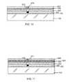
- the method 1000includes a process ( 1060 ) of forming a layer of photovoltaic material overlying the electrode layer.
- FIG. 7is a schematic diagram showing a process for fabricating a thin film photovoltaic cell according to an embodiment of the present invention. This diagram is merely an example, which should not unduly limit the scope of the claims herein.
- a layer of photovoltaic material 500is formed overlying the lower electrode layer 200 .
- a pattern 250 formed by laser ablation (process 1030 ) in the lower electrode layer 200can be filled with a conductive material to form an interconnect structure 270 .
- the interconnect structurecan serve as an electrical lead for collecting current from a thin film solar cell to be formed with the layer of photovoltaic material.
- the layer of photovoltaic material 500is made of copper indium diselenide (CIS) material using a sputtering and a thermal annealing based selenization process.
- the layer of photovoltaic material 500comprises a copper indium gallium diselenide (CIGS) material, or copper indium disulfide material using one or more suitable thin film deposition processes.
- the layer of photovoltaic material 500is a p-type semiconductor material acting as an light absorber of a thin film photovoltaic device.
- the layer of CIGS material formed on (the lower electrode layer over) the soda lime glass substratecan have large grain sizes larger than 1 microns. Therefore, high cell current can be expected for achieving 17% or greater efficiency for the resulted thin film solar cell.
- the method 1000includes a process ( 1070 ) of forming an upper electrode layer over the layer of photovoltaic material.
- the upper electrode layer or the second electrode layeris a first zinc oxide layer which is a kind of transparent conductive oxide or TCO.
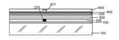
- the process 1070leads to a formation of the second electrode layer 600 overlying the layer of photovoltaic material 500 .
- FIG. 8is merely an example, which should not unduly limit the scope of the claims herein.
- the second electrode layer 600is a first zinc oxide layer.
- the first zinc oxide layeris formed using a metalorganic chemical vapor deposition (MOCVD) technique within a batch system.
- MOCVDmetalorganic chemical vapor deposition
- the formed first zinc oxide layer by MOCVDis a rough layer, which can diffuse the incoming light by scattering, increasing the efficiency of solar cells.
- the first zinc oxide layer 600can be mechanically patterned to form one or more patterns which in additions are used to form at least another interconnect structure 670 for the thin film photovoltaic cell, shown as an example in FIG. 8 .
- the method 1000then can include a process 1070 for any additional step of fabricating a thin film photovoltaic device.
- the process 1070can be another mechanical patterning for configuring the second or upper electrode layer, can be a mechanical isocut process for preparing one or more unit cells, and can be a mechanical bus pad cleaning process for assembling the one or more unit cells.
- the process 1070can be another mechanical patterning for configuring the second or upper electrode layer, can be a mechanical isocut process for preparing one or more unit cells, and can be a mechanical bus pad cleaning process for assembling the one or more unit cells.
- the method 1000may include a process of forming a barrier layer directly onto the surface region (after a pre-washing treatment process) of the soda lime glass substrate before the process 1020 for forming a lower electrode layer.
- FIG. 9shows a process of fabricating a thin film photovoltaic cell on soda lime glass substrate according to an alternative embodiment of the present invention. This diagram is merely an example, which should not unduly limit the scope of the claims herein. One of ordinary skill in the art would recognize many variations, alternatives, and modifications. As shown, a barrier layer 150 is inserted between the lower electrode layer 200 and the surface region 101 of the soda lime glass substrate 100 .
- the barrier layer 150is applied for preventing sodium element from diffusing into the upper layers especially the layer of photovoltaic material.
- the barrier layer 150is a layer of silicon dioxide formed by a sputtering process, which serves as an effective sodium diffusion barrier with a thickness of only about 200 Angstroms or greater.
- Other materialsincluding aluminum oxide, silicon nitride, titanium nitride, titanium oxide, or zirconium oxide also can be used depending on applications.
- the barrier layer propertycan be engineered or adjusted to improve the effectiveness of blocking sodium ion diffusion from glass into photovoltaic active layers.
- the barrier layer densitycan be a factor utilized. Higher barrier layer density can be used to raise the diffusion barrier and limit the amount of sodium diffusion.
- the method 1000can include a process of forming a cadmium sulfide layer overlying the layer of photovoltaic material before forming the first zinc oxide layer.
- the layer of photovoltaic material 500is a layer of copper indium diselenide material overlying the lower electrode molybdenum layer 200 .
- the cadmium sulfide layer 505characterized as a wide bandgap semiconductor, is formed over the layer of copper indium diselenide material 500 to serve as a window layer for the thin film photovoltaic cell while the layer of copper indium diselenide material 500 acting as an absorber layer.
- the cadmium sulfide layer 505is considered as one part of the layer of photovoltaic material which is formed using a multilayer deposition and treatment process.
- the cadmium sulfide layer 505can be formed using sputtering, vacuum evaporation, or chemical bath deposition (CBD) techniques and doped with n + -type impurities for conductivity.
- the window layercan be selected from a group materials consisting of a cadmium sulfide (CdS), a zinc sulfide (ZnS), zinc selenium (ZnSe), zinc oxide (ZnO), zinc magnesium oxide (ZnMgO), or others.
- the method 1000can include a process of forming a second zinc oxide layer before forming the first zinc oxide layer.
- the second zinc oxide layer 605is first formed over the layer of photovoltaic material, or in particular over the cadmium sulfide layer 505 , and the first zinc oxide layer 600 is formed over the second oxide layer 605 .
- the layer of photovoltaic material 500is a layer of copper indium diselenide material overlying the lower electrode molybdenum layer 200 .
- the second zinc oxide layer 605has a higher resistivity than the first zinc oxide layer 600 .
- the second zinc oxide layer 605plays more a role of barrier/protection layer while the first zinc oxide layer 600 with lower resisitivity plays more a role of conductive electrode layer.
- the second zinc oxide layer 605is also formed using a metalorganic chemical vapor deposition (MOCVD) technique within a batch system.
- MOCVDmetalorganic chemical vapor deposition
Landscapes
- Photovoltaic Devices (AREA)
Abstract
Description
- This application claims priority to U.S. Provisional Patent Application No. 61/101,650, filed Sep. 30, 2008, entitled “PATTERNING ELECTRODE MATERIALS FREE FROM BERM STRUCTURES FOR THIN FILM PHOTOVOLTAIC CELLS” by inventor Robert D. Wieting, commonly assigned and incorporated by reference herein for all purposes.
- NOT APPLICABLE
- NOT APPLICABLE
- The present invention relates generally to photovoltaic materials and manufacturing method. More particularly, the present invention provides a method and structure for fabricating thin film solar cells. Merely by way of example, the present method includes patterning electrode material free from berm structures for manufacture of thin film photovoltaic cells, but it would be recognized that the invention may have other configurations.
- From the beginning of time, mankind has been challenged to find way of harnessing energy. Energy comes in the forms such as petrochemical, hydroelectric, nuclear, wind, biomass, solar, and more primitive forms such as wood and coal. Over the past century, modern civilization has relied upon petrochemical energy as an important energy source. Petrochemical energy includes gas and oil. Gas includes lighter forms such as butane and propane, commonly used to heat homes and serve as fuel for cooking. Gas also includes gasoline, diesel, and jet fuel, commonly used for transportation purposes. Heavier forms of petrochemicals can also be used to heat homes in some places. Unfortunately, the supply of petrochemical fuel is limited and essentially fixed based upon the amount available on the planet Earth. Additionally, as more people use petroleum products in growing amounts, it is rapidly becoming a scarce resource, which will eventually become depleted over time.
- More recently, environmentally clean and renewable sources of energy have been desired. An example of a clean source of energy is hydroelectric power. Hydroelectric power is derived from electric generators driven by the flow of water produced by dams such as the Hoover Dam in Nevada. The electric power generated is used to power a large portion of the city of Los Angeles in California. Clean and renewable sources of energy also include wind, waves, biomass, and the like. That is, windmills convert wind energy into more useful forms of energy such as electricity. Still other types of clean energy include solar energy. Specific details of solar energy can be found throughout the present background and more particularly below.
- Solar energy technology generally converts electromagnetic radiation from the sun to other useful forms of energy. These other forms of energy include thermal energy and electrical power. For electrical power applications, solar cells are often used. Although solar energy is environmentally clean and has been successful to a point, many limitations remain to be resolved before it becomes widely used throughout the world. As an example, one type of solar cell uses crystalline materials, which are derived from semiconductor material ingots. These crystalline materials can be used to fabricate optoelectronic devices that include photovoltaic and photodiode devices that convert electromagnetic radiation into electrical power. However, crystalline materials are often costly and difficult to make on a large scale. Additionally, devices made from such crystalline materials often have low energy conversion efficiencies. Other types of solar cells use “thin film” technology to form a thin film of photosensitive material to be used to convert electromagnetic radiation into electrical power. Similar limitations exist with the use of thin film technology in making solar cells. That is, efficiencies are often poor. Additionally, film reliability is often poor and cannot be used for extensive periods of time in conventional environmental applications. Often, thin films are difficult to mechanically integrate with each other. Furthermore, thin films are often difficult to manufacture in a cost effective, efficient, and reliable way. These and other limitations of these conventional technologies can be found throughout the present specification and more particularly below.
- The present invention relates generally to photovoltaic materials and manufacturing method. More particularly, the present invention provides a method and structure for fabricating thin film solar cells. Merely by way of example, the present method includes patterning electrode material free from berm structures for manufacture of thin film photovoltaic cells, but it would be recognized that the invention may have other configurations.
- In a specific embodiment, the present invention provides a method for forming a thin film photovoltaic device having patterned electrode films. The method includes providing a soda lime glass substrate comprising a surface region and forming a lower electrode layer comprising a molybdenum material overlying the surface region. The method further includes subjecting the lower electrode layer with one or more pulses of electromagnetic radiation from a laser source. The one or more pulses of electromagnetic radiation is capable of ablating one or more patterns from the lower electrode layer. The one or more patterns includes one or more berm structures. Additionally, the method includes processing the lower electrode layer comprising the one or more patterns using a mechanical brush device to remove the one or more berm structures. The method further includes treating the lower electrode layer comprising the one or more patterns free from the one or more berm structures. Furthermore, the method includes forming a layer of photovoltaic material overlying the lower electrode layer. The layer of photovoltaic material comprising an interconnect structure based on the one or more patterns within the lower electrode layer. Moreover, the method includes forming a first zinc oxide layer overlying the layer of photovoltaic material.
- In another specific embodiment, the present invention provides a method for forming a thin film photovoltaic device having patterned electrode films. The method includes providing a soda lime glass substrate comprising a surface region and forming a lower electrode layer comprising a molybdenum material overlying the surface region. The method also includes subjecting the lower electrode layer with one or more pulses of electromagnetic radiation from a laser source for ablating one or more patterns from the lower electrode layer. The one or more patterns includes one or more berm structures. Additionally, the method includes processing the lower electrode layer comprising the one or more patterns using a mechanical brush device and a cleaning liquid to remove the one or more berm structures. Furthermore, the method includes processing the lower electrode layer comprising the one or more patterns free from the one or more berm structures using a gas knife. The gas knife is configured to remove substantially any liquid including liquid droplets from a surface of the lower electrode layer to dry the lower electrode layer comprising the one or more patterns free from the one or more berm structures.
- Many benefits are achieved by ways of present invention. For example, the present invention uses starting materials that are commercially available to form a thin film of semiconductor bearing material overlying a suitable substrate member. The thin film of semiconductor bearing material can be further processed to form a semiconductor thin film material of desired characteristics, such as atomic stoichiometry, impurity concentration, carrier concentration, doping, and others. In a specific embodiment, the present invention provides a resulting structure that is reliable and free from berm structures and the like. In preferred embodiments, the present invention uses commonly used tools and process technology. Depending on the embodiment, one or more of the benefits can be achieved. These and other benefits will be described in more detailed throughout the present specification and particularly below.
- Merely by way of example, the present method and materials include absorber materials made of copper indium disulfide species, copper tin sulfide, iron disulfide, or others for single junction cells or multi junction cells.
FIG. 1 is a simplified flowchart illustrating a method of fabricating a thin film photovoltaic cell according to an embodiment of the present invention;FIGS. 2-4 ,4A,5,5A,6,6A, and7-11 are schematic diagrams illustrating a method comprising a series of processes and structures for fabricating a thin film photovoltaic cell according to certain embodiments of the present invention.- The present invention relates generally to photovoltaic materials and manufacturing method. More particularly, the present invention provides a method and structure for fabricating thin film solar cells. Merely by way of example, the present method includes patterning electrode material formed on a soda lime glass substrate using electromagnetic radiations and processing the electrode material free from berm structures for manufacture of thin film photovoltaic cells, but it would be recognized that the invention may have other configurations.
FIG. 1 is a simplified flowchart illustrating a method of fabricating a thin film photovoltaic cell according to an embodiment of the present invention. This diagram is merely an example, which should not unduly limit the scope of the claims herein. Themethod 1000 includes the following processes:- 1.
Process 1010 for providing a soda lime glass substrate with a surface region; - 2.
Process 1020 for forming a lower electrode layer overlying the surface region; - 3.
Process 1030 for subjecting the lower electrode layer with a laser radiation to ablate one or more patterns; - 4.
Process 1040 for processing the lower electrode layer to remove one or more berm structures of the one or more patterns; - 5.
Process 1050 for treating the lower electrode layer with the one or more patterns free of the one or more berm structures; - 6.
Process 1060 for forming a layer of photovoltaic material comprising an interconnect structure based on each of the one or more patterns; - 7.
Process 1070 for forming a first zinc oxide layer overlying the layer of photovoltaic material; - 8.
Process 1080 for performing other steps.
- 1.
- The above sequence of processes provides a method of patterning an electrode layer and processing the electrode layer to form one or more patterns free of berm structures for manufacture of thin film photovoltaic cells according to an embodiment of the present invention. In a specific embodiment, the method includes applying laser radiations for ablating the one or more patterns from a continuous electrode layer. In another specific embodiment, the method also includes using mechanical brush device for processing the one or more patterns. Other alternatives can also be provided where processes are added, one or more processes are removed, or one or more processes are provided in a different sequence without departing from the scope of the claims herein. For example, a barrier layer can be formed before the lower electrode layer is formed. More functional layers with different material compositions can be inserted between the layer of photovoltaic material and the first zinc oxide layer, and so on. Further details of the method can be found throughout the present specification and more particularly below.
- At
Process 1010, a soda lime glass substrate is provided. This process can be visually illustrated byFIG. 2 .FIG. 2 is a simplified diagram illustrating a soda lime glass substrate provided for fabricating a thin film photovoltaic cell according to an embodiment of the present invention. This diagram is merely an example, which should not unduly limit the scope of the claims herein. One of ordinary skill in the art would recognize many variations, alternatives, and modifications. As shown, the sodalime glass substrate 100 including asurface region 101 is provided. The soda lime glass has been widely used as window glass. One important reason for choosing the soda lime glass as substrate for forming thin film photovoltaic cells other than simple economical concern is a positive influence of alkaline ions (e.g., Na+) on the grain growth of high efficiency thin film photovoltaic materials. For example, polycrystalline compound semiconductor films of chalcopyrite structure CuIn(Ga)Se2or CuInSe2materials can be formed on soda lime glass substrates with coarse grain sizes of 1 microns or larger so that high cell current can be collected with these photovoltaic films to have light-conversion efficiencies of 17% or above. Without the doping of sodium atoms, the same film material formed on other type of substrate has much finer sized grains. In certain implementations, thesurface region 101 is subjected to certain pre-treatment process so that thesurface region 101 is cleaned substantially free from surface contaminations, greases, dirts, dusts and particles having sizes larger than 3 microns. - At
Process 1020, a lower electrode layer is formed overlying the surface region of the soda lime glass substrate. This process can be visually illustrated byFIG. 3 . As shown, thelower electrode layer 200 is formed overlying thesurface region 101 of the sodalime glass substrate 100. Thelower electrode layer 200 is to serve a back electrode for thin film photovoltaic cells to be formed in subsequent processes. Here “lower” is merely a word for current example of forming a thin film on substrate, the thin film is to become a bottom solar cell. “Lower” electrode may correspond to an “upper” or “front” electrode that is located on top of a window layer. While when the substrate is used as “superstrate” in an application of forming a top solar cell, the lower or upper electrodes can be disposed in opposite way. In certain cases when no confusion, only electrode layer is mentioned. In particular, either the lower or upper electrode layer can be optically transparent. For example, the lower electrode layer is made of molybdenum material with thickness ranging from 0.2 to 1 microns. In other examples, transparent conductive oxide can be used as the material for upper electrode layer. In certain implementations, the formation of the electrode layer can be achieved using a deposition process, such as sputtering, plating, evaporation, plasma deposition, and the like and any other suitable technique. Of course, there can be other variations, modifications, and alternatives. - In the next process (1030), the
method 1000 includes subjecting the lower electrode layer with a laser radiation to ablate one or more patterns. This laser patterning or ablation process can be visually illustrated byFIG. 4 .FIG. 4 is a schematic diagram illustrating a process for fabricating a thin film photovoltaic cell according to an embodiment of the present invention. This diagram is merely an example, which should not unduly limit the scope of the claims herein. One of ordinary skill in the art would recognize many variations, alternatives, and modifications. As shown, thelower electrode layer 200 is subjected to alaser radiation 120 at certain predetermined locations. Thelaser radiation 120 can be a beam of pulsed laser or CW laser. The laser beam can be aligned from above thelower electrode layer 200 or from a back surface region of the sodalime glass substrate 100 for the glass is optically transparent. This laser alignment option is depended on the design of a manufacture system and specific thin film growth processes. Typically the laser beam is generated from a Nd: YAG infrared Q-Switched pulse laser source with wavelength of about 1065 nm. Of course, other types of laser sources with different wavelength or pulse rate can also be used depending on applications. - In one embodiment, the
laser beam 120 irradiating thelower electrode layer 200 causes an ablation process in which a portion of the lower electrode layer under the laser beam is removed from the sodalime glass substrate 100. In particular, the laser energy causes vaporization of electrode layer material, e.g., molybdenum, under a beam spot or simply blows away from thesubstrate 100. Thelaser beam 120 can be scanned along a predetermined pattern and subsequently additional amount of electrode layer material is removed. Each time after the laser beam ablates a spot of electrode layer material, the beam is moved (may be pulsed OFF) to a next spot, then the laser power is pulsed ON to irradiate the new spot again to cause the electrode layer material under the new spot to be removed. As a result, theelectrode layer 200, which is initially deposited as a continues film overlying thesurface region 101 of the sodalime glass substrate 100, is going through a laser patterning process to form one or more patterns (or laser ablated patterns). - As shown in the side view portion of the
FIG. 4 , one of the one ormore patterns 250 is schematically illustrated, separating theelectrode layer 200 into aleft portion 200A and aright portion 200B. An enlarged top view shows more details of a circled portion of aparticular pattern 250 that separates thelower electrode layer 200 to the twoportions pattern 250 is actually a continuous line with a width of about 25 to 50 microns of the lower electrode layer with being substantially removed from the glass substrate by the laser ablation process. As a result, a street structure is ormed within theelectrode layer 200. In certain embodiments, multiple streets with an average separation of about 6 mm are formed in the electrode layer overlying the whole surface region of the soda lime glass substrate, defining a stripe-shaped cell between each neighboring streets. - Due to laser beam spatial profile and pulse/scan variation, one or
more berm structures 255 are formed within thepattern 250. In a specific embodiment, the one ormore berm structures 255 usually are located near edges of thepattern 250, while some may also be left near the middle region of thepattern 250. As shown, the one ormore berm structures 255 have irregular shapes. Depending on the applications, the one ormore berm structures 255 may include residue material of theelectrode layer 250 or contaminants from a system housing the soda lime glass substrate. Because of theberm structures 255 are electrically conductive, they may causes electrical shorting of thin film devices if they are not substantially cleaned or freed by a suitable process. FIG. 4A is a microscope image showing a laser ablated pattern formed on a thin film over a glass substrate. As shown, the laser ablated pattern is created by irradiating a round laser spot on the thin film to remove the thin film material under the spot at least partially. Additionally, the laser spot is allowed to scan from one spot to next, thereby removing thin film material along the way. Provided a certain scanning speed of the laser beam, a street or a channeled pattern is formed. As a top view inFIG. 4A , thestreet 255 corresponds to the laser ablatedpattern 250 in thelower electrode layer 200 seen as a side view inFIG. 4 . However, imperfection during the laser ablation process may leave certain amount of residue/redeposit or un-removed portion of the thin film material forming one ormore berm structures 255 inside or around thelaser ablation pattern 250. Theseberm structures 255 may cause thin film device degradation, shorting or other problems. Embodiments of the present invention provide a method to substantially clean the laser ablation pattern free from these berm structures. More detail descriptions on the method can be found throughout this specification and more specifically below.- In the
next process 1040, themethod 1000 includes processing the lower electrode layer having one or more patterns to remove the one or more berm structures therein. This process can be visually illustrated byFIG. 5 .FIG. 5 is a schematic diagram illustrating a process for fabricating a thin film photovoltaic cell according to an embodiment of the present invention. This diagram is merely an example, which should not unduly limit the scope of the claims herein. One of ordinary skill in the art would recognize many variations, alternatives, and modifications. As shown inFIG. 5 a specific embodiment of themethod 1000 provides amechanical brush device 300 disposed above thelower electrode layer 200. Themechanical brush device 300 includes arotor 301 carrying an outer edge comprising a plurality ofbristles 305. In one embodiment, therotor 301 is powered to rotate alongclockwise direction 310 and at the same time is configured to laterally move along adirection 320 which is substantially in parallel to the surface of the soda lime glass substrate. In a specific embodiment, thebrush moving direction 320 can be either parallel or perpendicular to thelaser ablation pattern 250 for the purpose of effectively removing the debris or particles inside the pattern. Also shown, asprayer 350 is associated with the operation of themechanical brush device 300 to provide a liquid, de-ionized water in a preferred embodiment, during the brushing process. - In certain implementation of the
process 1040, themechanical brush device 300 can be disposed to a proper height above thelower electrode layer 200 and rolling the plurality ofbristles 305 with a predetermined rotation speed (along a direction310) while at the same time moving laterally with a predetermined lateral speed (along a direction320). Subsequently, themechanical brush device 300 is configured to adjust its height and lateral moving direction so that the one ormore berm structures 255 within or around the one ormore patterns 250 in various orientations and densities can be removed properly and as completely as possible. Of course, there can be other variations, alternatives and modifications in the control of rotation/lateral direction/speed, and configurations of the mechanical brush device including relative position of the rotor, a length of each bristle, supply of liquid from thesprayer 350, and so on. For example, the length of the brush bristles can be chosen to be sufficient to reach the depth of the laser scribed trench so that it can substantially clean up the debris (caused by laser ablation) inside the scribed region in addition to removing the berm structures on the surface region. - In a specific embodiment, the plurality of
bristles 305 are made of a nylon material. The mechanical strength of the nylon-based bristles provides necessary forces to remove the one or more berm structures which are scattered around and bonded to the substrate with relative small forces. While the nylon-based bristles also have relative flexibility by their nature, depending further on how to group a certain number of bristles together and how distribute them around the outer edge of themechanical brush device 300, so that the forces generated by these bristles would not cause injures to the remaining portions of lower electrode layer (e.g.,200A and200B), which bonded to are attached to the substrate with much stronger forces. Themechanical brush device 300 including nylon-basedbristles 305 according to an embodiment of the invention is able to consistently remove the one ormore berm structures 255 from the one ormore patterns 250 of the lower electrode layer made of molybdenum material. - In an alternative embodiment, the mechanical brush device can be applied from both sides of the transparent substrate. As schematically shown in
FIG. 5A , which is a side view illustrating a substrate being transferred along a plurality of rollers within a batch system. In this figure, onemechanical brush device 300A including awater sprayer 350A is applied from atop surface region 201 and anothermechanical brush device 300B, both of which can be substantially the same as themechanical brush device 300, is applied from bottom surface region of the substrate. In one example, thetop surface region 201 is a surface of thelower electrode layer 200 overlying thesubstrate 100. In another example, thetop surface region 201 includes one or more portions being part of the one ormore patterns 250 formed within thelower electrode layer 200. - Referring to
FIG. 1 , themethod 1000 further includes aprocess 1050 of treating the lower electrode layer with the one or more patterns free of the one or more berm structures. This process can be visually illustrated byFIG. 6 , which is a schematic diagram showing a process for fabricating a thin film photovoltaic cell according to an embodiment of the present invention. This diagram is merely an example, which should not unduly limit the scope of the claims herein. One of ordinary skill in the art would recognize many variations, alternatives, and modifications. As shown in a specific embodiment, part of thetreatment process 1050 involves a clean process during which the sodalime glass substrate 100 coated with anelectrode layer 200 is exposed to a cleaningliquid 400. In one implementation, the cleaningliquid 400 comprises at least DI-water that physically wash out and reactively desorb surface residues. Subsequently, another part of thetreatment process 1050 involves a process of applying an air knife blower to remove moisture and any dusts left on a surface region of theelectrode layer 200. - In one implementation, as schematically shown in
FIG. 6 , agas knife blower 360 is disposed near the surface region of theelectrode layer 200 including one ormore patterns 250 after the cleaning process using thecleaning solution 400. In one example, thegas knife 360 is an air knife with an elongated nozzle capable of providing a faceted profile of highspeed air flow 365. Theimpact air flow 365 with the faceted profile is very effective for drying and cleaning the surface region including one or more (stripe shaped) patterns. In another example, dry nitrogen can be the gas in the gas knife. In one embodiment, theair knife blower 360 is capable of adjusting an angle relative to thesurface region 201 for achieving a desirable drying/cleaning effect. For example, the angle between the faceted profile of the air relative to the surface can be adjusted from 90 degrees to somewhat 45 degrees or 30 degrees and lower to enhance the drying effect. In another example, an angle between the air flow direction and the laser scribing pattern can also be adjusted between 0 to 90 degrees to enhance the debris cleaning effect. In an alternative embodiment, air pressure control of theair knife blower 360 can be used during the debris removal process, especially for removing debris inside the laser scribed pattern region. In a specific embodiment, using theair knife blower 360 for drying the surface region can substantially remove any liquid including the residues of the cleaningliquid 400, water droplets, or other chemicals in liquid forms. In another specific embodiment, using theair knife blower 360 to remove the liquid introduced in the treating process can be accomplished by direct blowing away physically and substantially free from causing any evaporation. Thus, the drying effect according to the above implementation of embodiments of the invention results in substantially free of any moisture residue on the lower electrode layer including one or more patterns. - In another implementation, as schematically shown in
FIG. 6A , both sides of the substrate can be applied with the air knife blowers in the above drying/cleaning process. As shown, a substrate being transferred along a plurality of rollers within a batch system. The substrate has atop surface region 201 which is essentially a surface of thelower electrode layer 200 overlying the sodalime glass substrate 100 inFIG. 5 . Oneair knife blower 360A is applied from above thetop surface region 201 and anotherair knife blower 360B is applied from the bottom of the substrate. Essentially, the treatingprocess 1050 is a combined process including exposing the substrate to a cleaningliquid 400 and using anair knife blower 360 to dry the substrate including thelower electrode layer 200 with one ormore patterns 250. The treatment process results in thelower electrode layer 200 with one ormore patterns 250 substantially free from any one ormore berm structures 255 and any moisture residues. - Referring to
FIG. 1 again, themethod 1000 includes a process (1060) of forming a layer of photovoltaic material overlying the electrode layer. This process can be visually illustrated byFIG. 7 , which is a schematic diagram showing a process for fabricating a thin film photovoltaic cell according to an embodiment of the present invention. This diagram is merely an example, which should not unduly limit the scope of the claims herein. One of ordinary skill in the art would recognize many variations, alternatives, and modifications. As shown, a layer ofphotovoltaic material 500 is formed overlying thelower electrode layer 200. In particular, before or during theprocess 1060 of the formation of the layer ofphotovoltaic material 500, apattern 250 formed by laser ablation (process1030) in thelower electrode layer 200 can be filled with a conductive material to form aninterconnect structure 270. The interconnect structure can serve as an electrical lead for collecting current from a thin film solar cell to be formed with the layer of photovoltaic material. In a specific embodiment, the layer ofphotovoltaic material 500 is made of copper indium diselenide (CIS) material using a sputtering and a thermal annealing based selenization process. In another specific embodiment, the layer ofphotovoltaic material 500 comprises a copper indium gallium diselenide (CIGS) material, or copper indium disulfide material using one or more suitable thin film deposition processes. In one typical implementation, the layer ofphotovoltaic material 500 is a p-type semiconductor material acting as an light absorber of a thin film photovoltaic device. In one embodiment, with a certain amount of sodium content doped therein, the layer of CIGS material formed on (the lower electrode layer over) the soda lime glass substrate can have large grain sizes larger than 1 microns. Therefore, high cell current can be expected for achieving 17% or greater efficiency for the resulted thin film solar cell. - Although the above has been generally described in terms of a specific structure for CIS and/or CIGS thin film cells, other specific CIS and/or CIGS configurations can also be used, such as those noted in U.S. Pat. No. 4,612,411 and U.S. Pat. No. 4,611,091, which are hereby incorporated by reference herein, without departing from the invention described by the claims herein.
- Furthermore, the
method 1000 includes a process (1070) of forming an upper electrode layer over the layer of photovoltaic material. Here the upper electrode layer or the second electrode layer is a first zinc oxide layer which is a kind of transparent conductive oxide or TCO. As shown inFIG. 8 , subsequent toprocess 1060, theprocess 1070 leads to a formation of thesecond electrode layer 600 overlying the layer ofphotovoltaic material 500.FIG. 8 is merely an example, which should not unduly limit the scope of the claims herein. One of ordinary skill in the art would recognize many variations, alternatives, and modifications. In a specific embodiment, thesecond electrode layer 600 is a first zinc oxide layer. In one example, the first zinc oxide layer is formed using a metalorganic chemical vapor deposition (MOCVD) technique within a batch system. The formed first zinc oxide layer by MOCVD is a rough layer, which can diffuse the incoming light by scattering, increasing the efficiency of solar cells. Additionally, the firstzinc oxide layer 600 can be mechanically patterned to form one or more patterns which in additions are used to form at least anotherinterconnect structure 670 for the thin film photovoltaic cell, shown as an example inFIG. 8 . - The
method 1000 then can include aprocess 1070 for any additional step of fabricating a thin film photovoltaic device. For example, theprocess 1070 can be another mechanical patterning for configuring the second or upper electrode layer, can be a mechanical isocut process for preparing one or more unit cells, and can be a mechanical bus pad cleaning process for assembling the one or more unit cells. Of course, there can be many variations, alternatives, and modifications. - In an alternative embodiment, the
method 1000 may include a process of forming a barrier layer directly onto the surface region (after a pre-washing treatment process) of the soda lime glass substrate before theprocess 1020 for forming a lower electrode layer.FIG. 9 shows a process of fabricating a thin film photovoltaic cell on soda lime glass substrate according to an alternative embodiment of the present invention. This diagram is merely an example, which should not unduly limit the scope of the claims herein. One of ordinary skill in the art would recognize many variations, alternatives, and modifications. As shown, abarrier layer 150 is inserted between thelower electrode layer 200 and thesurface region 101 of the sodalime glass substrate 100. Because excessive, uncontrolled amount of sodium may reduce the grain sizes of the photovoltaic thin film grown on the soda lime glass substrate, thebarrier layer 150 is applied for preventing sodium element from diffusing into the upper layers especially the layer of photovoltaic material. In one embodiment, thebarrier layer 150 is a layer of silicon dioxide formed by a sputtering process, which serves as an effective sodium diffusion barrier with a thickness of only about 200 Angstroms or greater. Other materials including aluminum oxide, silicon nitride, titanium nitride, titanium oxide, or zirconium oxide also can be used depending on applications. In an alternative embodiment, the barrier layer property can be engineered or adjusted to improve the effectiveness of blocking sodium ion diffusion from glass into photovoltaic active layers. For example, the barrier layer density can be a factor utilized. Higher barrier layer density can be used to raise the diffusion barrier and limit the amount of sodium diffusion. - In another alternative embodiment, the
method 1000 can include a process of forming a cadmium sulfide layer overlying the layer of photovoltaic material before forming the first zinc oxide layer. In particular, as shown inFIG. 10 the layer ofphotovoltaic material 500 is a layer of copper indium diselenide material overlying the lowerelectrode molybdenum layer 200. Thecadmium sulfide layer 505, characterized as a wide bandgap semiconductor, is formed over the layer of copperindium diselenide material 500 to serve as a window layer for the thin film photovoltaic cell while the layer of copperindium diselenide material 500 acting as an absorber layer. In certain embodiments, thecadmium sulfide layer 505 is considered as one part of the layer of photovoltaic material which is formed using a multilayer deposition and treatment process. In one example, thecadmium sulfide layer 505 can be formed using sputtering, vacuum evaporation, or chemical bath deposition (CBD) techniques and doped with n+-type impurities for conductivity. Depending on embodiments, the window layer can be selected from a group materials consisting of a cadmium sulfide (CdS), a zinc sulfide (ZnS), zinc selenium (ZnSe), zinc oxide (ZnO), zinc magnesium oxide (ZnMgO), or others. - In yet another alternative embodiment, the
method 1000 can include a process of forming a second zinc oxide layer before forming the first zinc oxide layer. As shown inFIG. 11 the secondzinc oxide layer 605 is first formed over the layer of photovoltaic material, or in particular over thecadmium sulfide layer 505, and the firstzinc oxide layer 600 is formed over thesecond oxide layer 605. The layer ofphotovoltaic material 500 is a layer of copper indium diselenide material overlying the lowerelectrode molybdenum layer 200. In a specific embodiment, the secondzinc oxide layer 605 has a higher resistivity than the firstzinc oxide layer 600. Functionally, the secondzinc oxide layer 605 plays more a role of barrier/protection layer while the firstzinc oxide layer 600 with lower resisitivity plays more a role of conductive electrode layer. In certain embodiment, the secondzinc oxide layer 605 is also formed using a metalorganic chemical vapor deposition (MOCVD) technique within a batch system. - Although the above has been illustrated according to specific embodiments, there can be other modifications, alternatives, and variations. It is understood that the examples and embodiments described herein are for illustrative purposes only and that various modifications or changes in light thereof will be suggested to persons skilled in the art and are to be included within the spirit and purview of this application and scope of the appended claims.
Claims (22)
Priority Applications (2)
| Application Number | Priority Date | Filing Date | Title |
|---|---|---|---|
| US12/565,735US7863074B2 (en) | 2008-09-30 | 2009-09-23 | Patterning electrode materials free from berm structures for thin film photovoltaic cells |
| US12/962,580US8435822B2 (en) | 2008-09-30 | 2010-12-07 | Patterning electrode materials free from berm structures for thin film photovoltaic cells |
Applications Claiming Priority (2)
| Application Number | Priority Date | Filing Date | Title |
|---|---|---|---|
| US10165008P | 2008-09-30 | 2008-09-30 | |
| US12/565,735US7863074B2 (en) | 2008-09-30 | 2009-09-23 | Patterning electrode materials free from berm structures for thin film photovoltaic cells |
Related Child Applications (1)
| Application Number | Title | Priority Date | Filing Date |
|---|---|---|---|
| US12/962,580ContinuationUS8435822B2 (en) | 2008-09-30 | 2010-12-07 | Patterning electrode materials free from berm structures for thin film photovoltaic cells |
Publications (2)
| Publication Number | Publication Date |
|---|---|
| US20100261307A1true US20100261307A1 (en) | 2010-10-14 |
| US7863074B2 US7863074B2 (en) | 2011-01-04 |
Family
ID=42073867
Family Applications (2)
| Application Number | Title | Priority Date | Filing Date |
|---|---|---|---|
| US12/565,735Expired - Fee RelatedUS7863074B2 (en) | 2008-09-30 | 2009-09-23 | Patterning electrode materials free from berm structures for thin film photovoltaic cells |
| US12/962,580Expired - Fee RelatedUS8435822B2 (en) | 2008-09-30 | 2010-12-07 | Patterning electrode materials free from berm structures for thin film photovoltaic cells |
Family Applications After (1)
| Application Number | Title | Priority Date | Filing Date |
|---|---|---|---|
| US12/962,580Expired - Fee RelatedUS8435822B2 (en) | 2008-09-30 | 2010-12-07 | Patterning electrode materials free from berm structures for thin film photovoltaic cells |
Country Status (4)
| Country | Link |
|---|---|
| US (2) | US7863074B2 (en) |
| CN (1) | CN102160186B (en) |
| DE (1) | DE112009002290T5 (en) |
| WO (1) | WO2010039879A1 (en) |
Cited By (2)
| Publication number | Priority date | Publication date | Assignee | Title |
|---|---|---|---|---|
| US20130052768A1 (en)* | 2011-08-24 | 2013-02-28 | Applied Materials, Inc. | High speed laser scanning system for silicon solar cell fabrication |
| US11211507B2 (en)* | 2016-04-29 | 2021-12-28 | Stichting Energieonderzoek Centrum Nederland | Method for manufacturing interconnected solar cells and such interconnected solar cells |
Families Citing this family (53)
| Publication number | Priority date | Publication date | Assignee | Title |
|---|---|---|---|---|
| US8017860B2 (en) | 2006-05-15 | 2011-09-13 | Stion Corporation | Method and structure for thin film photovoltaic materials using bulk semiconductor materials |
| US20080300918A1 (en)* | 2007-05-29 | 2008-12-04 | Commercenet Consortium, Inc. | System and method for facilitating hospital scheduling and support |
| US8071179B2 (en) | 2007-06-29 | 2011-12-06 | Stion Corporation | Methods for infusing one or more materials into nano-voids if nanoporous or nanostructured materials |
| US8058092B2 (en)* | 2007-09-28 | 2011-11-15 | Stion Corporation | Method and material for processing iron disilicide for photovoltaic application |
| US8759671B2 (en)* | 2007-09-28 | 2014-06-24 | Stion Corporation | Thin film metal oxide bearing semiconductor material for single junction solar cell devices |
| US8287942B1 (en) | 2007-09-28 | 2012-10-16 | Stion Corporation | Method for manufacture of semiconductor bearing thin film material |
| US8614396B2 (en)* | 2007-09-28 | 2013-12-24 | Stion Corporation | Method and material for purifying iron disilicide for photovoltaic application |
| US20110017298A1 (en)* | 2007-11-14 | 2011-01-27 | Stion Corporation | Multi-junction solar cell devices |
| US7998762B1 (en) | 2007-11-14 | 2011-08-16 | Stion Corporation | Method and system for large scale manufacture of thin film photovoltaic devices using multi-chamber configuration |
| DE102008015807A1 (en)* | 2008-03-27 | 2009-10-22 | Schott Solar Gmbh | Process for structuring the zinc oxide front electrode layer of a photovoltaic module |
| US20090301562A1 (en)* | 2008-06-05 | 2009-12-10 | Stion Corporation | High efficiency photovoltaic cell and manufacturing method |
| US8642138B2 (en) | 2008-06-11 | 2014-02-04 | Stion Corporation | Processing method for cleaning sulfur entities of contact regions |
| US9087943B2 (en)* | 2008-06-25 | 2015-07-21 | Stion Corporation | High efficiency photovoltaic cell and manufacturing method free of metal disulfide barrier material |
| US8003432B2 (en) | 2008-06-25 | 2011-08-23 | Stion Corporation | Consumable adhesive layer for thin film photovoltaic material |
| US20110017257A1 (en)* | 2008-08-27 | 2011-01-27 | Stion Corporation | Multi-junction solar module and method for current matching between a plurality of first photovoltaic devices and second photovoltaic devices |
| US20100051090A1 (en)* | 2008-08-28 | 2010-03-04 | Stion Corporation | Four terminal multi-junction thin film photovoltaic device and method |
| US7855089B2 (en)* | 2008-09-10 | 2010-12-21 | Stion Corporation | Application specific solar cell and method for manufacture using thin film photovoltaic materials |
| US8026122B1 (en) | 2008-09-29 | 2011-09-27 | Stion Corporation | Metal species surface treatment of thin film photovoltaic cell and manufacturing method |
| US8476104B1 (en) | 2008-09-29 | 2013-07-02 | Stion Corporation | Sodium species surface treatment of thin film photovoltaic cell and manufacturing method |
| US8008112B1 (en) | 2008-09-29 | 2011-08-30 | Stion Corporation | Bulk chloride species treatment of thin film photovoltaic cell and manufacturing method |
| US8394662B1 (en) | 2008-09-29 | 2013-03-12 | Stion Corporation | Chloride species surface treatment of thin film photovoltaic cell and manufacturing method |
| US8236597B1 (en) | 2008-09-29 | 2012-08-07 | Stion Corporation | Bulk metal species treatment of thin film photovoltaic cell and manufacturing method |
| US8008110B1 (en) | 2008-09-29 | 2011-08-30 | Stion Corporation | Bulk sodium species treatment of thin film photovoltaic cell and manufacturing method |
| US8501521B1 (en) | 2008-09-29 | 2013-08-06 | Stion Corporation | Copper species surface treatment of thin film photovoltaic cell and manufacturing method |
| US8569613B1 (en) | 2008-09-29 | 2013-10-29 | Stion Corporation | Multi-terminal photovoltaic module including independent cells and related system |
| US8008111B1 (en) | 2008-09-29 | 2011-08-30 | Stion Corporation | Bulk copper species treatment of thin film photovoltaic cell and manufacturing method |
| US7863074B2 (en)* | 2008-09-30 | 2011-01-04 | Stion Corporation | Patterning electrode materials free from berm structures for thin film photovoltaic cells |
| US8425739B1 (en) | 2008-09-30 | 2013-04-23 | Stion Corporation | In chamber sodium doping process and system for large scale cigs based thin film photovoltaic materials |
| US20100078059A1 (en)* | 2008-09-30 | 2010-04-01 | Stion Corporation | Method and structure for thin film tandem photovoltaic cell |
| US8232134B2 (en) | 2008-09-30 | 2012-07-31 | Stion Corporation | Rapid thermal method and device for thin film tandem cell |
| US7947524B2 (en)* | 2008-09-30 | 2011-05-24 | Stion Corporation | Humidity control and method for thin film photovoltaic materials |
| US8383450B2 (en)* | 2008-09-30 | 2013-02-26 | Stion Corporation | Large scale chemical bath system and method for cadmium sulfide processing of thin film photovoltaic materials |
| US7910399B1 (en)* | 2008-09-30 | 2011-03-22 | Stion Corporation | Thermal management and method for large scale processing of CIS and/or CIGS based thin films overlying glass substrates |
| US8741689B2 (en)* | 2008-10-01 | 2014-06-03 | Stion Corporation | Thermal pre-treatment process for soda lime glass substrate for thin film photovoltaic materials |
| US20110018103A1 (en) | 2008-10-02 | 2011-01-27 | Stion Corporation | System and method for transferring substrates in large scale processing of cigs and/or cis devices |
| US8003430B1 (en) | 2008-10-06 | 2011-08-23 | Stion Corporation | Sulfide species treatment of thin film photovoltaic cell and manufacturing method |
| US8435826B1 (en) | 2008-10-06 | 2013-05-07 | Stion Corporation | Bulk sulfide species treatment of thin film photovoltaic cell and manufacturing method |
| US8168463B2 (en) | 2008-10-17 | 2012-05-01 | Stion Corporation | Zinc oxide film method and structure for CIGS cell |
| US8344243B2 (en)* | 2008-11-20 | 2013-01-01 | Stion Corporation | Method and structure for thin film photovoltaic cell using similar material junction |
| US8563850B2 (en)* | 2009-03-16 | 2013-10-22 | Stion Corporation | Tandem photovoltaic cell and method using three glass substrate configuration |
| US8507786B1 (en) | 2009-06-27 | 2013-08-13 | Stion Corporation | Manufacturing method for patterning CIGS/CIS solar cells |
| US8398772B1 (en) | 2009-08-18 | 2013-03-19 | Stion Corporation | Method and structure for processing thin film PV cells with improved temperature uniformity |
| US8809096B1 (en) | 2009-10-22 | 2014-08-19 | Stion Corporation | Bell jar extraction tool method and apparatus for thin film photovoltaic materials |
| US8859880B2 (en) | 2010-01-22 | 2014-10-14 | Stion Corporation | Method and structure for tiling industrial thin-film solar devices |
| US8263494B2 (en) | 2010-01-25 | 2012-09-11 | Stion Corporation | Method for improved patterning accuracy for thin film photovoltaic panels |
| US9096930B2 (en) | 2010-03-29 | 2015-08-04 | Stion Corporation | Apparatus for manufacturing thin film photovoltaic devices |
| US8461061B2 (en) | 2010-07-23 | 2013-06-11 | Stion Corporation | Quartz boat method and apparatus for thin film thermal treatment |
| US8628997B2 (en) | 2010-10-01 | 2014-01-14 | Stion Corporation | Method and device for cadmium-free solar cells |
| GB201018141D0 (en) | 2010-10-27 | 2010-12-08 | Pilkington Group Ltd | Polishing coated substrates |
| DE102011008269B4 (en)* | 2011-01-11 | 2015-01-08 | Interpane Entwicklungs-Und Beratungsgesellschaft Mbh | Thin-film solar cells with diffusion-inhibiting coating |
| US8728200B1 (en) | 2011-01-14 | 2014-05-20 | Stion Corporation | Method and system for recycling processing gas for selenization of thin film photovoltaic materials |
| US8998606B2 (en) | 2011-01-14 | 2015-04-07 | Stion Corporation | Apparatus and method utilizing forced convection for uniform thermal treatment of thin film devices |
| US8436445B2 (en) | 2011-08-15 | 2013-05-07 | Stion Corporation | Method of manufacture of sodium doped CIGS/CIGSS absorber layers for high efficiency photovoltaic devices |
Citations (27)
| Publication number | Priority date | Publication date | Assignee | Title |
|---|---|---|---|---|
| US4996108A (en)* | 1989-01-17 | 1991-02-26 | Simon Fraser University | Sheets of transition metal dichalcogenides |
| US5125984A (en)* | 1990-05-31 | 1992-06-30 | Siemens Aktiengesellschaft | Induced junction chalcopyrite solar cell |
| US5261968A (en)* | 1992-01-13 | 1993-11-16 | Photon Energy, Inc. | Photovoltaic cell and method |
| US5501744A (en)* | 1992-01-13 | 1996-03-26 | Photon Energy, Inc. | Photovoltaic cell having a p-type polycrystalline layer with large crystals |
| US5536333A (en)* | 1992-05-12 | 1996-07-16 | Solar Cells, Inc. | Process for making photovoltaic devices and resultant product |
| US5622634A (en)* | 1993-12-17 | 1997-04-22 | Canon Kabushiki Kaisha | Method of manufacturing electron-emitting device, electron source and image-forming apparatus |
| US5665175A (en)* | 1990-05-30 | 1997-09-09 | Safir; Yakov | Bifacial solar cell |
| US5985691A (en)* | 1997-05-16 | 1999-11-16 | International Solar Electric Technology, Inc. | Method of making compound semiconductor films and making related electronic devices |
| US6328871B1 (en)* | 1999-08-16 | 2001-12-11 | Applied Materials, Inc. | Barrier layer for electroplating processes |
| US20020004302A1 (en)* | 1995-09-14 | 2002-01-10 | Yoshihiko Fukumoto | Method for fabricating semiconductor device |
| US6361718B1 (en)* | 1998-02-05 | 2002-03-26 | Nippon Sheet Glass Co., Ltd. | Article having uneven surface, production process for the article, and composition for the process |
| US20020061361A1 (en)* | 2000-09-06 | 2002-05-23 | Hiroki Nakahara | Method and apparatus for fabricating electro-optical device and method and apparatus for fabricating liquid crystal panel |
| US6423565B1 (en)* | 2000-05-30 | 2002-07-23 | Kurt L. Barth | Apparatus and processes for the massproduction of photovotaic modules |
| US6632113B1 (en)* | 1998-09-09 | 2003-10-14 | Canon Kabushiki Kaisha | Image display apparatus, disassembly processing method therefor, and component recovery method |
| US20060220059A1 (en)* | 2003-04-09 | 2006-10-05 | Matsushita Electric Industrial Co., Ltd | Solar cell |
| US20070089782A1 (en)* | 2003-10-02 | 2007-04-26 | Scheuten Glasgroep | Spherical or grain-shaped semiconductor element for use in solar cells and method for producing the same; method for producing a solar cell comprising said semiconductor element and solar cell |
| US20070151596A1 (en)* | 2004-02-20 | 2007-07-05 | Sharp Kabushiki Kaisha | Substrate for photoelectric conversion device, photoelectric conversion device, and stacked photoelectric conversion device |
| US20070169810A1 (en)* | 2004-02-19 | 2007-07-26 | Nanosolar, Inc. | High-throughput printing of semiconductor precursor layer by use of chalcogen-containing vapor |
| US7252923B2 (en)* | 2001-10-16 | 2007-08-07 | Dai Nippon Printing Co., Ltd. | Methods for producing pattern-forming body |
| US20080041446A1 (en)* | 2006-08-09 | 2008-02-21 | Industrial Technology Research Institute | Dye-sensitized solar cells and method for fabricating same |
| US20080092945A1 (en)* | 2006-10-24 | 2008-04-24 | Applied Quantum Technology Llc | Semiconductor Grain and Oxide Layer for Photovoltaic Cells |
| US20080092953A1 (en)* | 2006-05-15 | 2008-04-24 | Stion Corporation | Method and structure for thin film photovoltaic materials using bulk semiconductor materials |
| US7364808B2 (en)* | 2001-10-19 | 2008-04-29 | Asahi Glass Company, Limited | Substrate with transparent conductive oxide film, process for its production and photoelectric conversion element |
| US20080110491A1 (en)* | 2006-03-18 | 2008-05-15 | Solyndra, Inc., | Monolithic integration of non-planar solar cells |
| US20080210303A1 (en)* | 2006-11-02 | 2008-09-04 | Guardian Industries Corp. | Front electrode for use in photovoltaic device and method of making same |
| US7736755B2 (en)* | 2005-04-25 | 2010-06-15 | Fujifilm Corporation | Organic electroluminescent device |
| US7741560B2 (en)* | 2005-07-22 | 2010-06-22 | Honda Motor Co., Ltd. | Chalcopyrite solar cell |
Family Cites Families (218)
| Publication number | Priority date | Publication date | Assignee | Title |
|---|---|---|---|---|
| US3520732A (en) | 1965-10-22 | 1970-07-14 | Matsushita Electric Industrial Co Ltd | Photovoltaic cell and process of preparation of same |
| US3828722A (en) | 1970-05-01 | 1974-08-13 | Cogar Corp | Apparatus for producing ion-free insulating layers |
| US3975211A (en) | 1975-03-28 | 1976-08-17 | Westinghouse Electric Corporation | Solar cells and method for making same |
| US4062038A (en) | 1976-01-28 | 1977-12-06 | International Business Machines Corporation | Radiation responsive device |
| US4332974A (en) | 1979-06-28 | 1982-06-01 | Chevron Research Company | Multilayer photovoltaic cell |
| US5217564A (en) | 1980-04-10 | 1993-06-08 | Massachusetts Institute Of Technology | Method of producing sheets of crystalline material and devices made therefrom |
| EP0191503A3 (en) | 1980-04-10 | 1986-09-10 | Massachusetts Institute Of Technology | Method of producing sheets of crystalline material |
| US4335266A (en) | 1980-12-31 | 1982-06-15 | The Boeing Company | Methods for forming thin-film heterojunction solar cells from I-III-VI.sub.2 |
| US4441113A (en) | 1981-02-13 | 1984-04-03 | Energy Conversion Devices, Inc. | P-Type semiconductor material having a wide band gap |
| US4465575A (en) | 1981-09-21 | 1984-08-14 | Atlantic Richfield Company | Method for forming photovoltaic cells employing multinary semiconductor films |
| DE3314197A1 (en) | 1982-04-28 | 1983-11-03 | Energy Conversion Devices, Inc., 48084 Troy, Mich. | P-CONDUCTING AMORPHOUS SILICON ALLOY WITH A LARGE BAND GAP AND MANUFACTURING PROCESS THEREFOR |
| US4442310A (en) | 1982-07-15 | 1984-04-10 | Rca Corporation | Photodetector having enhanced back reflection |
| US4518855A (en) | 1982-09-30 | 1985-05-21 | Spring-Mornne, Inc. | Method and apparatus for statically aligning shafts and monitoring shaft alignment |
| US4461922A (en) | 1983-02-14 | 1984-07-24 | Atlantic Richfield Company | Solar cell module |
| US4471155A (en) | 1983-04-15 | 1984-09-11 | Energy Conversion Devices, Inc. | Narrow band gap photovoltaic devices with enhanced open circuit voltage |
| US4517403A (en) | 1983-05-16 | 1985-05-14 | Atlantic Richfield Company | Series connected solar cells and method of formation |
| US4724011A (en) | 1983-05-16 | 1988-02-09 | Atlantic Richfield Company | Solar cell interconnection by discrete conductive regions |
| US4532372A (en) | 1983-12-23 | 1985-07-30 | Energy Conversion Devices, Inc. | Barrier layer for photovoltaic devices |
| US4598306A (en) | 1983-07-28 | 1986-07-01 | Energy Conversion Devices, Inc. | Barrier layer for photovoltaic devices |
| US4499658A (en) | 1983-09-06 | 1985-02-19 | Atlantic Richfield Company | Solar cell laminates |
| US4589194A (en) | 1983-12-29 | 1986-05-20 | Atlantic Richfield Company | Ultrasonic scribing of thin film solar cells |
| US4542255A (en) | 1984-01-03 | 1985-09-17 | Atlantic Richfield Company | Gridded thin film solar cell |
| US4581108A (en) | 1984-01-06 | 1986-04-08 | Atlantic Richfield Company | Process of forming a compound semiconductive material |
| US4661370A (en) | 1984-02-08 | 1987-04-28 | Atlantic Richfield Company | Electric discharge processing of thin films |
| US4507181A (en) | 1984-02-17 | 1985-03-26 | Energy Conversion Devices, Inc. | Method of electro-coating a semiconductor device |
| US4611091A (en) | 1984-12-06 | 1986-09-09 | Atlantic Richfield Company | CuInSe2 thin film solar cell with thin CdS and transparent window layer |
| US4599154A (en) | 1985-03-15 | 1986-07-08 | Atlantic Richfield Company | Electrically enhanced liquid jet processing |
| US4663495A (en) | 1985-06-04 | 1987-05-05 | Atlantic Richfield Company | Transparent photovoltaic module |
| US4612411A (en) | 1985-06-04 | 1986-09-16 | Atlantic Richfield Company | Thin film solar cell with ZnO window layer |
| US4623601A (en) | 1985-06-04 | 1986-11-18 | Atlantic Richfield Company | Photoconductive device containing zinc oxide transparent conductive layer |
| US4638111A (en) | 1985-06-04 | 1987-01-20 | Atlantic Richfield Company | Thin film solar cell module |
| JPH0682625B2 (en) | 1985-06-04 | 1994-10-19 | シーメンス ソーラー インダストリーズ,エル.ピー. | Deposition method of zinc oxide film |
| US4798660A (en) | 1985-07-16 | 1989-01-17 | Atlantic Richfield Company | Method for forming Cu In Se2 films |
| US4625070A (en) | 1985-08-30 | 1986-11-25 | Atlantic Richfield Company | Laminated thin film solar module |
| JPS6273784A (en) | 1985-09-27 | 1987-04-04 | Sanyo Electric Co Ltd | photovoltaic device |
| US4865999A (en) | 1987-07-08 | 1989-09-12 | Glasstech Solar, Inc. | Solar cell fabrication method |
| US4775425A (en) | 1987-07-27 | 1988-10-04 | Energy Conversion Devices, Inc. | P and n-type microcrystalline semiconductor alloy material including band gap widening elements, devices utilizing same |
| US4816082A (en) | 1987-08-19 | 1989-03-28 | Energy Conversion Devices, Inc. | Thin film solar cell including a spatially modulated intrinsic layer |
| US4968354A (en) | 1987-11-09 | 1990-11-06 | Fuji Electric Co., Ltd. | Thin film solar cell array |
| US5045409A (en) | 1987-11-27 | 1991-09-03 | Atlantic Richfield Company | Process for making thin film solar cell |
| US4793283A (en) | 1987-12-10 | 1988-12-27 | Sarkozy Robert F | Apparatus for chemical vapor deposition with clean effluent and improved product yield |
| US5008062A (en) | 1988-01-20 | 1991-04-16 | Siemens Solar Industries, L.P. | Method of fabricating photovoltaic module |
| US5259883A (en) | 1988-02-16 | 1993-11-09 | Kabushiki Kaisha Toshiba | Method of thermally processing semiconductor wafers and an apparatus therefor |
| US4915745A (en) | 1988-09-22 | 1990-04-10 | Atlantic Richfield Company | Thin film solar cell and method of making |
| US5180686A (en) | 1988-10-31 | 1993-01-19 | Energy Conversion Devices, Inc. | Method for continuously deposting a transparent oxide material by chemical pyrolysis |
| US4873118A (en) | 1988-11-18 | 1989-10-10 | Atlantic Richfield Company | Oxygen glow treating of ZnO electrode for thin film silicon solar cell |
| US4950615A (en) | 1989-02-06 | 1990-08-21 | International Solar Electric Technology, Inc. | Method and making group IIB metal - telluride films and solar cells |
| FR2646560B1 (en) | 1989-04-27 | 1994-01-14 | Solems Sa | METHOD FOR IMPROVING THE SPECTRAL RESPONSE OF AN IMPROVED PHOTOCONDUCTOR STRUCTURE, SOLAR CELL AND PHOTORECEPTIVE STRUCTURE |
| US5028274A (en) | 1989-06-07 | 1991-07-02 | International Solar Electric Technology, Inc. | Group I-III-VI2 semiconductor films for solar cell application |
| DE69024304T2 (en) | 1989-09-06 | 1996-07-18 | Sanyo Electric Co | Manufacturing process for a flexible photovoltaic device |
| US5078803A (en) | 1989-09-22 | 1992-01-07 | Siemens Solar Industries L.P. | Solar cells incorporating transparent electrodes comprising hazy zinc oxide |
| JPH03124067A (en) | 1989-10-07 | 1991-05-27 | Showa Shell Sekiyu Kk | Photovoltaic device and its manufacture |
| US5011565A (en) | 1989-12-06 | 1991-04-30 | Mobil Solar Energy Corporation | Dotted contact solar cell and method of making same |
| US5154777A (en) | 1990-02-26 | 1992-10-13 | Mcdonnell Douglas Corporation | Advanced survivable space solar power system |
| DE59009771D1 (en) | 1990-07-24 | 1995-11-16 | Siemens Ag | Process for the manufacture of a chalcopyrite solar cell. |
| JP2729239B2 (en) | 1990-10-17 | 1998-03-18 | 昭和シェル石油株式会社 | Integrated photovoltaic device |
| US5528397A (en) | 1991-12-03 | 1996-06-18 | Kopin Corporation | Single crystal silicon transistors for display panels |
| US5336381A (en) | 1991-01-07 | 1994-08-09 | United Technologies Corporation | Electrophoresis process for preparation of ceramic fibers |
| US6784492B1 (en) | 1991-03-18 | 2004-08-31 | Canon Kabushiki Kaisha | Semiconductor device including a gate-insulated transistor |
| JPH0788063A (en) | 1991-05-08 | 1995-04-04 | Sharp Corp | Handle mounting structure |
| US5211824A (en) | 1991-10-31 | 1993-05-18 | Siemens Solar Industries L.P. | Method and apparatus for sputtering of a liquid |
| US5231047A (en) | 1991-12-19 | 1993-07-27 | Energy Conversion Devices, Inc. | High quality photovoltaic semiconductor material and laser ablation method of fabrication same |
| JPH05243596A (en) | 1992-03-02 | 1993-09-21 | Showa Shell Sekiyu Kk | Manufacture of laminated type solar cell |
| JP2756050B2 (en) | 1992-03-03 | 1998-05-25 | キヤノン株式会社 | Photovoltaic device |
| WO1993019491A1 (en) | 1992-03-19 | 1993-09-30 | Siemens Solar Gmbh | Weather-resistant thin layer solar module |
| US5298086A (en) | 1992-05-15 | 1994-03-29 | United Solar Systems Corporation | Method for the manufacture of improved efficiency tandem photovoltaic device and device manufactured thereby |
| EP0574716B1 (en) | 1992-05-19 | 1996-08-21 | Matsushita Electric Industrial Co., Ltd. | Method for preparing chalcopyrite-type compound |
| EP0648373B1 (en) | 1992-06-29 | 2002-01-30 | United Solar Systems Corporation | Microwave energized deposition process with substrate temperature control |
| ATE170669T1 (en) | 1992-06-29 | 1998-09-15 | Canon Kk | RESIN COMPOSITION FOR SEALING AND A SEMICONDUCTOR DEVICE COVERED WITH SEALING RESIN COMPOSITION |
| US5578503A (en) | 1992-09-22 | 1996-11-26 | Siemens Aktiengesellschaft | Rapid process for producing a chalcopyrite semiconductor on a substrate |
| US5474939A (en) | 1992-12-30 | 1995-12-12 | Siemens Solar Industries International | Method of making thin film heterojunction solar cell |
| US5436204A (en) | 1993-04-12 | 1995-07-25 | Midwest Research Institute | Recrystallization method to selenization of thin-film Cu(In,Ga)Se2 for semiconductor device applications |
| DE4333407C1 (en) | 1993-09-30 | 1994-11-17 | Siemens Ag | Solar cell comprising a chalcopyrite absorber layer |
| US5738731A (en) | 1993-11-19 | 1998-04-14 | Mega Chips Corporation | Photovoltaic device |
| US5578103A (en) | 1994-08-17 | 1996-11-26 | Corning Incorporated | Alkali metal ion migration control |
| DE4442824C1 (en) | 1994-12-01 | 1996-01-25 | Siemens Ag | Solar cell having higher degree of activity |
| US5698496A (en) | 1995-02-10 | 1997-12-16 | Lucent Technologies Inc. | Method for making an anisotropically conductive composite medium |
| EP0729189A1 (en) | 1995-02-21 | 1996-08-28 | Interuniversitair Micro-Elektronica Centrum Vzw | Method of preparing solar cells and products obtained thereof |
| US5674325A (en) | 1995-06-07 | 1997-10-07 | Photon Energy, Inc. | Thin film photovoltaic device and process of manufacture |
| US5625688A (en)* | 1995-06-15 | 1997-04-29 | Jing Mei Industrial Holdings, Ltd. | Shower telephone |
| US5977476A (en) | 1996-10-16 | 1999-11-02 | United Solar Systems Corporation | High efficiency photovoltaic device |
| JP3249408B2 (en) | 1996-10-25 | 2002-01-21 | 昭和シェル石油株式会社 | Method and apparatus for manufacturing thin film light absorbing layer of thin film solar cell |
| JP3249407B2 (en) | 1996-10-25 | 2002-01-21 | 昭和シェル石油株式会社 | Thin-film solar cells composed of chalcopyrite-based multi-compound semiconductor thin-film light-absorbing layers |
| JP3527815B2 (en) | 1996-11-08 | 2004-05-17 | 昭和シェル石油株式会社 | Method for producing transparent conductive film of thin film solar cell |
| US5925228A (en) | 1997-01-09 | 1999-07-20 | Sandia Corporation | Electrophoretically active sol-gel processes to backfill, seal, and/or densify porous, flawed, and/or cracked coatings on electrically conductive material |
| JPH1154773A (en) | 1997-08-01 | 1999-02-26 | Canon Inc | Photovoltaic element and method for manufacturing the same |
| DE19741832A1 (en) | 1997-09-23 | 1999-03-25 | Inst Solarenergieforschung | Method of manufacturing a solar cell and solar cell |
| US6258620B1 (en) | 1997-10-15 | 2001-07-10 | University Of South Florida | Method of manufacturing CIGS photovoltaic devices |
| JP2001523049A (en) | 1997-11-10 | 2001-11-20 | スターメガ コーポレイション | Quantum ridges and quantum peaks |
| US6107562A (en) | 1998-03-24 | 2000-08-22 | Matsushita Electric Industrial Co., Ltd. | Semiconductor thin film, method for manufacturing the same, and solar cell using the same |
| US6344608B2 (en) | 1998-06-30 | 2002-02-05 | Canon Kabushiki Kaisha | Photovoltaic element |
| US6127202A (en) | 1998-07-02 | 2000-10-03 | International Solar Electronic Technology, Inc. | Oxide-based method of making compound semiconductor films and making related electronic devices |
| US6451415B1 (en) | 1998-08-19 | 2002-09-17 | The Trustees Of Princeton University | Organic photosensitive optoelectronic device with an exciton blocking layer |
| US6323417B1 (en) | 1998-09-29 | 2001-11-27 | Lockheed Martin Corporation | Method of making I-III-VI semiconductor materials for use in photovoltaic cells |
| JP2000150861A (en) | 1998-11-16 | 2000-05-30 | Tdk Corp | Oxide thin film |
| JP3667178B2 (en) | 1998-11-24 | 2005-07-06 | キヤノン株式会社 | Method for producing zinc oxide thin film, method for producing photovoltaic element using the same, and photovoltaic element |
| JP2000173969A (en) | 1998-12-03 | 2000-06-23 | Canon Inc | Rinse method and photovoltaic device |
| JP2001156321A (en) | 1999-03-09 | 2001-06-08 | Fuji Xerox Co Ltd | Semiconductor device and method of manufacturing the same |
| US6160215A (en) | 1999-03-26 | 2000-12-12 | Curtin; Lawrence F. | Method of making photovoltaic device |
| US6307148B1 (en) | 1999-03-29 | 2001-10-23 | Shinko Electric Industries Co., Ltd. | Compound semiconductor solar cell and production method thereof |
| WO2001057932A1 (en) | 2000-02-07 | 2001-08-09 | Cis Solartechnik Gmbh | Flexible metal substrate for cis solar cells, and method for producing the same |
| US6372538B1 (en) | 2000-03-16 | 2002-04-16 | University Of Delaware | Fabrication of thin-film, flexible photovoltaic module |
| US7194197B1 (en) | 2000-03-16 | 2007-03-20 | Global Solar Energy, Inc. | Nozzle-based, vapor-phase, plume delivery structure for use in production of thin-film deposition layer |
| US7414188B2 (en) | 2002-01-25 | 2008-08-19 | Konarka Technologies, Inc. | Co-sensitizers for dye sensitized solar cells |
| US7301199B2 (en) | 2000-08-22 | 2007-11-27 | President And Fellows Of Harvard College | Nanoscale wires and related devices |
| CN101798057A (en) | 2000-08-22 | 2010-08-11 | 哈佛学院董事会 | Doped elongated semiconductors, growing such semiconductors, devices including such semiconductors and fabricating such devices |
| US6576112B2 (en) | 2000-09-19 | 2003-06-10 | Canon Kabushiki Kaisha | Method of forming zinc oxide film and process for producing photovoltaic device using it |
| JP2002167695A (en) | 2000-09-19 | 2002-06-11 | Canon Inc | Method for forming zinc oxide film and method for manufacturing photovoltaic element using the same |
| DE10104726A1 (en) | 2001-02-02 | 2002-08-08 | Siemens Solar Gmbh | Process for structuring an oxide layer applied to a carrier material |
| US6858308B2 (en) | 2001-03-12 | 2005-02-22 | Canon Kabushiki Kaisha | Semiconductor element, and method of forming silicon-based film |
| JP4827303B2 (en) | 2001-03-12 | 2011-11-30 | キヤノン株式会社 | Photovoltaic element, TFT, and method for forming i-type semiconductor layer |
| JP2002299670A (en) | 2001-04-03 | 2002-10-11 | Canon Inc | Silicon based thin film and photovoltaic device |
| US7842882B2 (en) | 2004-03-01 | 2010-11-30 | Basol Bulent M | Low cost and high throughput deposition methods and apparatus for high density semiconductor film growth |
| US7053294B2 (en) | 2001-07-13 | 2006-05-30 | Midwest Research Institute | Thin-film solar cell fabricated on a flexible metallic substrate |
| US6635307B2 (en) | 2001-12-12 | 2003-10-21 | Nanotek Instruments, Inc. | Manufacturing method for thin-film solar cells |
| US7276749B2 (en) | 2002-02-05 | 2007-10-02 | E-Phocus, Inc. | Image sensor with microcrystalline germanium photodiode layer |
| US6690041B2 (en) | 2002-05-14 | 2004-02-10 | Global Solar Energy, Inc. | Monolithically integrated diodes in thin-film photovoltaic devices |
| US7560641B2 (en) | 2002-06-17 | 2009-07-14 | Shalini Menezes | Thin film solar cell configuration and fabrication method |
| US7291782B2 (en) | 2002-06-22 | 2007-11-06 | Nanosolar, Inc. | Optoelectronic device and fabrication method |
| US6852920B2 (en) | 2002-06-22 | 2005-02-08 | Nanosolar, Inc. | Nano-architected/assembled solar electricity cell |
| WO2004022637A2 (en) | 2002-09-05 | 2004-03-18 | Nanosys, Inc. | Nanocomposites |
| TW200425530A (en) | 2002-09-05 | 2004-11-16 | Nanosys Inc | Nanostructure and nanocomposite based compositions and photovoltaic devices |
| EP1556902A4 (en) | 2002-09-30 | 2009-07-29 | Miasole | APPARATUS AND METHOD FOR MANUFACTURING CON CURRENT FOR LARGE SCALE PRODUCTION OF THIN FILM SOLAR CELLS |
| JP3570515B2 (en) | 2002-10-15 | 2004-09-29 | セイコーエプソン株式会社 | Method and apparatus for forming porous insulating film and electronic device manufactured using the method |
| US6849798B2 (en) | 2002-12-17 | 2005-02-01 | General Electric Company | Photovoltaic cell using stable Cu2O nanocrystals and conductive polymers |
| US6936761B2 (en) | 2003-03-29 | 2005-08-30 | Nanosolar, Inc. | Transparent electrode, optoelectronic apparatus and devices |
| US7279832B2 (en) | 2003-04-01 | 2007-10-09 | Innovalight, Inc. | Phosphor materials and illumination devices made therefrom |
| US20040252488A1 (en) | 2003-04-01 | 2004-12-16 | Innovalight | Light-emitting ceiling tile |
| US7811606B2 (en)* | 2003-04-16 | 2010-10-12 | Dey, L.P. | Nasal pharmaceutical formulations and methods of using the same |
| JP2004332043A (en) | 2003-05-07 | 2004-11-25 | Canon Inc | Method and apparatus for forming zinc oxide thin film, and method for forming photovoltaic element |
| US7462774B2 (en) | 2003-05-21 | 2008-12-09 | Nanosolar, Inc. | Photovoltaic devices fabricated from insulating nanostructured template |
| US7265037B2 (en) | 2003-06-20 | 2007-09-04 | The Regents Of The University Of California | Nanowire array and nanowire solar cells and methods for forming the same |
| KR100838805B1 (en) | 2003-07-14 | 2008-06-17 | 가부시키가이샤후지쿠라 | Electrolyte composition, photoelectric conversion element and dye-sensitized solar cell using same |
| AU2003300775A1 (en) | 2003-09-03 | 2005-04-21 | Midwest Research Institute | Zno/cu(inga)se2 solar cells prepared by vapor phase zn doping |
| US8623448B2 (en) | 2004-02-19 | 2014-01-07 | Nanosolar, Inc. | High-throughput printing of semiconductor precursor layer from chalcogenide microflake particles |
| US20070163643A1 (en) | 2004-02-19 | 2007-07-19 | Nanosolar, Inc. | High-throughput printing of chalcogen layer and the use of an inter-metallic material |
| US7122398B1 (en) | 2004-03-25 | 2006-10-17 | Nanosolar, Inc. | Manufacturing of optoelectronic devices |
| JP2005311292A (en) | 2004-03-25 | 2005-11-04 | Kaneka Corp | Substrate for thin film solar cell, manufacturing method therefor, and thin film solar cell using the same |
| JP4695850B2 (en) | 2004-04-28 | 2011-06-08 | 本田技研工業株式会社 | Chalcopyrite solar cell |
| CN100463230C (en) | 2004-05-11 | 2009-02-18 | 本田技研工业株式会社 | Manufacturing method of chalcopyrite type thin film solar cell |
| EP1797584A4 (en) | 2004-06-08 | 2014-08-13 | Sandisk Corp | METHODS AND DEVICES FOR FORMING NANOSTRUCTURE MONOLAYERS AND DEVICES COMPRISING SUCH SINGLES |
| TWI406890B (en) | 2004-06-08 | 2013-09-01 | Sandisk Corp | Post-deposition encapsulation of nanostructures : compositions, devices and systems incorporating same |
| DE112005001429T5 (en) | 2004-06-18 | 2007-04-26 | Innovalight, Inc., St. Paul | Method and apparatus for forming nanoparticles using radio frequency plasmas |
| US7442320B2 (en) | 2004-06-18 | 2008-10-28 | Ultradots, Inc. | Nanostructured materials and photovoltaic devices including nanostructured materials |
| JP2006049768A (en) | 2004-08-09 | 2006-02-16 | Showa Shell Sekiyu Kk | CIS-based compound semiconductor thin film solar cell and method for producing light absorption layer of solar cell |
| US7750352B2 (en) | 2004-08-10 | 2010-07-06 | Pinion Technologies, Inc. | Light strips for lighting and backlighting applications |
| US7276724B2 (en) | 2005-01-20 | 2007-10-02 | Nanosolar, Inc. | Series interconnected optoelectronic device module assembly |
| US7732229B2 (en) | 2004-09-18 | 2010-06-08 | Nanosolar, Inc. | Formation of solar cells with conductive barrier layers and foil substrates |
| US20060249202A1 (en) | 2004-09-20 | 2006-11-09 | Seunghyup Yoo | Photovoltaic cell |
| US20060096536A1 (en) | 2004-11-10 | 2006-05-11 | Daystar Technologies, Inc. | Pressure control system in a photovoltaic substrate deposition apparatus |
| CN101233260A (en) | 2004-11-10 | 2008-07-30 | 德斯塔尔科技公司 | Pressure control system in photovoltaic substrate deposition |
| WO2006053032A1 (en) | 2004-11-10 | 2006-05-18 | Daystar Technologies, Inc. | Thermal process for creation of an in-situ junction layer in cigs |
| CA2586970A1 (en) | 2004-11-10 | 2006-05-18 | Daystar Technologies, Inc. | Vertical production of photovoltaic devices |
| US20060219288A1 (en) | 2004-11-10 | 2006-10-05 | Daystar Technologies, Inc. | Process and photovoltaic device using an akali-containing layer |
| US20060112983A1 (en) | 2004-11-17 | 2006-06-01 | Nanosys, Inc. | Photoactive devices and components with enhanced efficiency |
| US20060130890A1 (en) | 2004-12-20 | 2006-06-22 | Palo Alto Research Center Incorporated. | Heterojunction photovoltaic cell |
| JP2006179626A (en) | 2004-12-22 | 2006-07-06 | Showa Shell Sekiyu Kk | CIS-based thin-film solar cell module, method for producing the solar cell module, and separation method |
| JP2006186200A (en) | 2004-12-28 | 2006-07-13 | Showa Shell Sekiyu Kk | Precursor film and film forming method thereof |
| JP4131965B2 (en) | 2004-12-28 | 2008-08-13 | 昭和シェル石油株式会社 | Method for producing light absorption layer of CIS thin film solar cell |
| JP2006183117A (en) | 2004-12-28 | 2006-07-13 | Showa Shell Sekiyu Kk | Manufacturing method of ZnO-based transparent conductive film by MOCVD (metal organic chemical vapor deposition) |
| KR100495925B1 (en) | 2005-01-12 | 2005-06-17 | (주)인솔라텍 | Optical absorber layers for solar cell and manufacturing method thereof |
| JP5010806B2 (en) | 2005-02-01 | 2012-08-29 | 日本ペイント株式会社 | Powder coating composition and method for coating aluminum wheel |
| JP4841173B2 (en) | 2005-05-27 | 2011-12-21 | 昭和シェル石油株式会社 | High resistance buffer layer / window layer continuous film forming method and film forming apparatus for CIS thin film solar cell |
| WO2007019188A2 (en) | 2005-08-05 | 2007-02-15 | First Solar, Inc. | Manufacture of photovoltaic devices |
| FR2890232A1 (en) | 2005-08-23 | 2007-03-02 | Saint Gobain | COPLANAR DISCHARGE PLANE LAMP AND USES THEREFOR |
| JP2007123721A (en) | 2005-10-31 | 2007-05-17 | Rohm Co Ltd | Method for manufacturing photoelectric conversion device and photoelectric conversion device |
| US7442413B2 (en) | 2005-11-18 | 2008-10-28 | Daystar Technologies, Inc. | Methods and apparatus for treating a work piece with a vaporous element |
| DE102005062977B3 (en) | 2005-12-28 | 2007-09-13 | Sulfurcell Solartechnik Gmbh | Method and apparatus for converting metallic precursor layers to chalcopyrite layers of CIGSS solar cells |
| US8389852B2 (en) | 2006-02-22 | 2013-03-05 | Guardian Industries Corp. | Electrode structure for use in electronic device and method of making same |
| US9105776B2 (en) | 2006-05-15 | 2015-08-11 | Stion Corporation | Method and structure for thin film photovoltaic materials using semiconductor materials |
| US8617640B2 (en) | 2006-06-12 | 2013-12-31 | Nanosolar, Inc. | Thin-film devices formed from solid group IIIA alloy particles |
| US7879685B2 (en) | 2006-08-04 | 2011-02-01 | Solyndra, Inc. | System and method for creating electric isolation between layers comprising solar cells |
| DE102006041046A1 (en) | 2006-09-01 | 2008-03-06 | Cis Solartechnik Gmbh & Co. Kg | Solar cell, process for the production of solar cells and electrical trace |
| US8076571B2 (en) | 2006-11-02 | 2011-12-13 | Guardian Industries Corp. | Front electrode for use in photovoltaic device and method of making same |
| FR2908406B1 (en) | 2006-11-14 | 2012-08-24 | Saint Gobain | POROUS LAYER, METHOD FOR MANUFACTURING THE SAME, AND APPLICATIONS THEREOF |
| US20080121264A1 (en) | 2006-11-28 | 2008-05-29 | Industrial Technology Research Institute | Thin film solar module and method of fabricating the same |
| MX2009006725A (en) | 2006-12-21 | 2009-06-30 | Helianthos Bv | METHOD FOR PREPARING SOLAR SUB-CELLS FROM A SOLAR CELL. |
| WO2008095146A2 (en) | 2007-01-31 | 2008-08-07 | Van Duren Jeroen K J | Solar cell absorber layer formed from metal ion precursors |
| US20080204696A1 (en) | 2007-02-28 | 2008-08-28 | Tdk Corporation | Method of alignment |
| KR100882668B1 (en) | 2007-07-18 | 2009-02-06 | 삼성모바일디스플레이주식회사 | Organic light emitting display device and manufacturing method thereof |
| FR2919429B1 (en) | 2007-07-27 | 2009-10-09 | Saint Gobain | FRONT PANEL SUBSTRATE OF PHOTOVOLTAIC CELL AND USE OF A SUBSTRATE FOR A FRONT PANEL OF PHOTOVOLTAIC CELL |
| US8287942B1 (en) | 2007-09-28 | 2012-10-16 | Stion Corporation | Method for manufacture of semiconductor bearing thin film material |
| US20090087939A1 (en) | 2007-09-28 | 2009-04-02 | Stion Corporation | Column structure thin film material using metal oxide bearing semiconductor material for solar cell devices |
| JP2009099476A (en) | 2007-10-19 | 2009-05-07 | Sony Corp | Dye-sensitized photoelectric conversion element and method for producing the same |
| US7998762B1 (en) | 2007-11-14 | 2011-08-16 | Stion Corporation | Method and system for large scale manufacture of thin film photovoltaic devices using multi-chamber configuration |
| JP2009135337A (en) | 2007-11-30 | 2009-06-18 | Showa Shell Sekiyu Kk | Laminated structure of CIS solar cell, integrated structure of CIS thin film solar cell, and manufacturing method |
| US8001283B2 (en) | 2008-03-12 | 2011-08-16 | Mips Technologies, Inc. | Efficient, scalable and high performance mechanism for handling IO requests |
| US8981211B2 (en) | 2008-03-18 | 2015-03-17 | Zetta Research and Development LLC—AQT Series | Interlayer design for epitaxial growth of semiconductor layers |
| US20090235987A1 (en) | 2008-03-24 | 2009-09-24 | Epv Solar, Inc. | Chemical Treatments to Enhance Photovoltaic Performance of CIGS |
| US20090255467A1 (en) | 2008-04-15 | 2009-10-15 | Global Solar Energy, Inc. | Apparatus and methods for manufacturing thin-film solar cells |
| JP4384237B2 (en) | 2008-05-19 | 2009-12-16 | 昭和シェル石油株式会社 | CIS type thin film solar cell manufacturing method |
| FR2932009B1 (en) | 2008-06-02 | 2010-09-17 | Saint Gobain | PHOTOVOLTAIC CELL AND PHOTOVOLTAIC CELL SUBSTRATE |
| US8003432B2 (en) | 2008-06-25 | 2011-08-23 | Stion Corporation | Consumable adhesive layer for thin film photovoltaic material |
| US7855089B2 (en) | 2008-09-10 | 2010-12-21 | Stion Corporation | Application specific solar cell and method for manufacture using thin film photovoltaic materials |
| US8008111B1 (en) | 2008-09-29 | 2011-08-30 | Stion Corporation | Bulk copper species treatment of thin film photovoltaic cell and manufacturing method |
| US8008110B1 (en) | 2008-09-29 | 2011-08-30 | Stion Corporation | Bulk sodium species treatment of thin film photovoltaic cell and manufacturing method |
| US8008112B1 (en) | 2008-09-29 | 2011-08-30 | Stion Corporation | Bulk chloride species treatment of thin film photovoltaic cell and manufacturing method |
| US7863074B2 (en)* | 2008-09-30 | 2011-01-04 | Stion Corporation | Patterning electrode materials free from berm structures for thin film photovoltaic cells |
| US8217261B2 (en)* | 2008-09-30 | 2012-07-10 | Stion Corporation | Thin film sodium species barrier method and structure for cigs based thin film photovoltaic cell |
| US7947524B2 (en) | 2008-09-30 | 2011-05-24 | Stion Corporation | Humidity control and method for thin film photovoltaic materials |
| US8053274B2 (en) | 2008-09-30 | 2011-11-08 | Stion Corporation | Self cleaning large scale method and furnace system for selenization of thin film photovoltaic materials |
| US7910399B1 (en) | 2008-09-30 | 2011-03-22 | Stion Corporation | Thermal management and method for large scale processing of CIS and/or CIGS based thin films overlying glass substrates |
| US7960204B2 (en) | 2008-09-30 | 2011-06-14 | Stion Corporation | Method and structure for adhesion of absorber material for thin film photovoltaic cell |
| US8741689B2 (en)* | 2008-10-01 | 2014-06-03 | Stion Corporation | Thermal pre-treatment process for soda lime glass substrate for thin film photovoltaic materials |
| US20110018103A1 (en) | 2008-10-02 | 2011-01-27 | Stion Corporation | System and method for transferring substrates in large scale processing of cigs and/or cis devices |
| US8003430B1 (en) | 2008-10-06 | 2011-08-23 | Stion Corporation | Sulfide species treatment of thin film photovoltaic cell and manufacturing method |
| US8168463B2 (en) | 2008-10-17 | 2012-05-01 | Stion Corporation | Zinc oxide film method and structure for CIGS cell |
| US8344243B2 (en) | 2008-11-20 | 2013-01-01 | Stion Corporation | Method and structure for thin film photovoltaic cell using similar material junction |
| US20100197051A1 (en) | 2009-02-04 | 2010-08-05 | Applied Materials, Inc. | Metrology and inspection suite for a solar production line |
| US8197912B2 (en) | 2009-03-12 | 2012-06-12 | International Business Machines Corporation | Precision separation of PV thin film stacks |
| US8859880B2 (en) | 2010-01-22 | 2014-10-14 | Stion Corporation | Method and structure for tiling industrial thin-film solar devices |
| US8263494B2 (en) | 2010-01-25 | 2012-09-11 | Stion Corporation | Method for improved patterning accuracy for thin film photovoltaic panels |
| US9096930B2 (en) | 2010-03-29 | 2015-08-04 | Stion Corporation | Apparatus for manufacturing thin film photovoltaic devices |
| US8142521B2 (en) | 2010-03-29 | 2012-03-27 | Stion Corporation | Large scale MOCVD system for thin film photovoltaic devices |
| US20110259395A1 (en) | 2010-04-21 | 2011-10-27 | Stion Corporation | Single Junction CIGS/CIS Solar Module |
| US20110259413A1 (en) | 2010-04-21 | 2011-10-27 | Stion Corporation | Hazy Zinc Oxide Film for Shaped CIGS/CIS Solar Cells |
| US8461061B2 (en) | 2010-07-23 | 2013-06-11 | Stion Corporation | Quartz boat method and apparatus for thin film thermal treatment |
| US8628997B2 (en) | 2010-10-01 | 2014-01-14 | Stion Corporation | Method and device for cadmium-free solar cells |
- 2009
- 2009-09-23USUS12/565,735patent/US7863074B2/ennot_activeExpired - Fee Related
- 2009-09-30DEDE112009002290Tpatent/DE112009002290T5/ennot_activeCeased
- 2009-09-30WOPCT/US2009/059095patent/WO2010039879A1/enactiveApplication Filing
- 2009-09-30CNCN200980136265.1Apatent/CN102160186B/ennot_activeExpired - Fee Related
- 2010
- 2010-12-07USUS12/962,580patent/US8435822B2/ennot_activeExpired - Fee Related
Patent Citations (28)
| Publication number | Priority date | Publication date | Assignee | Title |
|---|---|---|---|---|
| US4996108A (en)* | 1989-01-17 | 1991-02-26 | Simon Fraser University | Sheets of transition metal dichalcogenides |
| US5665175A (en)* | 1990-05-30 | 1997-09-09 | Safir; Yakov | Bifacial solar cell |
| US5125984A (en)* | 1990-05-31 | 1992-06-30 | Siemens Aktiengesellschaft | Induced junction chalcopyrite solar cell |
| US5261968A (en)* | 1992-01-13 | 1993-11-16 | Photon Energy, Inc. | Photovoltaic cell and method |
| US5501744A (en)* | 1992-01-13 | 1996-03-26 | Photon Energy, Inc. | Photovoltaic cell having a p-type polycrystalline layer with large crystals |
| US5536333A (en)* | 1992-05-12 | 1996-07-16 | Solar Cells, Inc. | Process for making photovoltaic devices and resultant product |
| US5622634A (en)* | 1993-12-17 | 1997-04-22 | Canon Kabushiki Kaisha | Method of manufacturing electron-emitting device, electron source and image-forming apparatus |
| US20020004302A1 (en)* | 1995-09-14 | 2002-01-10 | Yoshihiko Fukumoto | Method for fabricating semiconductor device |
| US5985691A (en)* | 1997-05-16 | 1999-11-16 | International Solar Electric Technology, Inc. | Method of making compound semiconductor films and making related electronic devices |
| US6361718B1 (en)* | 1998-02-05 | 2002-03-26 | Nippon Sheet Glass Co., Ltd. | Article having uneven surface, production process for the article, and composition for the process |
| US6632113B1 (en)* | 1998-09-09 | 2003-10-14 | Canon Kabushiki Kaisha | Image display apparatus, disassembly processing method therefor, and component recovery method |
| US6328871B1 (en)* | 1999-08-16 | 2001-12-11 | Applied Materials, Inc. | Barrier layer for electroplating processes |
| US6423565B1 (en)* | 2000-05-30 | 2002-07-23 | Kurt L. Barth | Apparatus and processes for the massproduction of photovotaic modules |
| US7220321B2 (en)* | 2000-05-30 | 2007-05-22 | Barth Kurt L | Apparatus and processes for the mass production of photovoltaic modules |
| US20020061361A1 (en)* | 2000-09-06 | 2002-05-23 | Hiroki Nakahara | Method and apparatus for fabricating electro-optical device and method and apparatus for fabricating liquid crystal panel |
| US7252923B2 (en)* | 2001-10-16 | 2007-08-07 | Dai Nippon Printing Co., Ltd. | Methods for producing pattern-forming body |
| US7364808B2 (en)* | 2001-10-19 | 2008-04-29 | Asahi Glass Company, Limited | Substrate with transparent conductive oxide film, process for its production and photoelectric conversion element |
| US20060220059A1 (en)* | 2003-04-09 | 2006-10-05 | Matsushita Electric Industrial Co., Ltd | Solar cell |
| US20070089782A1 (en)* | 2003-10-02 | 2007-04-26 | Scheuten Glasgroep | Spherical or grain-shaped semiconductor element for use in solar cells and method for producing the same; method for producing a solar cell comprising said semiconductor element and solar cell |
| US20070169810A1 (en)* | 2004-02-19 | 2007-07-26 | Nanosolar, Inc. | High-throughput printing of semiconductor precursor layer by use of chalcogen-containing vapor |
| US20070151596A1 (en)* | 2004-02-20 | 2007-07-05 | Sharp Kabushiki Kaisha | Substrate for photoelectric conversion device, photoelectric conversion device, and stacked photoelectric conversion device |
| US7736755B2 (en)* | 2005-04-25 | 2010-06-15 | Fujifilm Corporation | Organic electroluminescent device |
| US7741560B2 (en)* | 2005-07-22 | 2010-06-22 | Honda Motor Co., Ltd. | Chalcopyrite solar cell |
| US20080110491A1 (en)* | 2006-03-18 | 2008-05-15 | Solyndra, Inc., | Monolithic integration of non-planar solar cells |
| US20080092953A1 (en)* | 2006-05-15 | 2008-04-24 | Stion Corporation | Method and structure for thin film photovoltaic materials using bulk semiconductor materials |
| US20080041446A1 (en)* | 2006-08-09 | 2008-02-21 | Industrial Technology Research Institute | Dye-sensitized solar cells and method for fabricating same |
| US20080092945A1 (en)* | 2006-10-24 | 2008-04-24 | Applied Quantum Technology Llc | Semiconductor Grain and Oxide Layer for Photovoltaic Cells |
| US20080210303A1 (en)* | 2006-11-02 | 2008-09-04 | Guardian Industries Corp. | Front electrode for use in photovoltaic device and method of making same |
Cited By (2)
| Publication number | Priority date | Publication date | Assignee | Title |
|---|---|---|---|---|
| US20130052768A1 (en)* | 2011-08-24 | 2013-02-28 | Applied Materials, Inc. | High speed laser scanning system for silicon solar cell fabrication |
| US11211507B2 (en)* | 2016-04-29 | 2021-12-28 | Stichting Energieonderzoek Centrum Nederland | Method for manufacturing interconnected solar cells and such interconnected solar cells |
Also Published As
| Publication number | Publication date |
|---|---|
| US7863074B2 (en) | 2011-01-04 |
| US20110073181A1 (en) | 2011-03-31 |
| CN102160186A (en) | 2011-08-17 |
| DE112009002290T5 (en) | 2011-09-29 |
| US8435822B2 (en) | 2013-05-07 |
| CN102160186B (en) | 2014-08-06 |
| WO2010039879A1 (en) | 2010-04-08 |
Similar Documents
| Publication | Publication Date | Title |
|---|---|---|
| US7863074B2 (en) | Patterning electrode materials free from berm structures for thin film photovoltaic cells | |
| US8217261B2 (en) | Thin film sodium species barrier method and structure for cigs based thin film photovoltaic cell | |
| US8741689B2 (en) | Thermal pre-treatment process for soda lime glass substrate for thin film photovoltaic materials | |
| US8309390B2 (en) | Method of manufacturing a photovoltaic device and system for patterning an object | |
| CN103762270B (en) | Solaode and manufacture method thereof | |
| US8691618B2 (en) | Metal species surface treatment of thin film photovoltaic cell and manufacturing method | |
| CN102479825B (en) | Solar cell and method for manufacturing same | |
| US20140216542A1 (en) | Semiconductor material surface treatment with laser | |
| US20110180122A1 (en) | Floating grid module design for thin film silicon solar cells | |
| US9761752B2 (en) | Solar cell, solar cell module, method for manufacturing solar cell, and method for manufacturing solar cell module | |
| WO2013039912A1 (en) | Laser annealing for thin film solar cells | |
| CN102934240B (en) | For the manufacture of the modification method of photovoltaic cell comprising tco layer | |
| US20130199608A1 (en) | Method for manufacturing a photovoltaic cell comprising a tco layer | |
| US11233165B2 (en) | Multi-junction solar cell and manufacturing method of the same | |
| US8236597B1 (en) | Bulk metal species treatment of thin film photovoltaic cell and manufacturing method | |
| US9257584B2 (en) | Solar cell interconnects and method of fabricating same | |
| US8642138B2 (en) | Processing method for cleaning sulfur entities of contact regions | |
| KR101326964B1 (en) | Solar cell module and method of fabricating the same | |
| JP2014067855A (en) | Photoelectric conversion device |
Legal Events
| Date | Code | Title | Description |
|---|---|---|---|
| AS | Assignment | Owner name:STION CORPORATION, CALIFORNIA Free format text:ASSIGNMENT OF ASSIGNORS INTEREST;ASSIGNOR:WIETING, ROBERT D.;REEL/FRAME:023458/0727 Effective date:20091023 | |
| STCF | Information on status: patent grant | Free format text:PATENTED CASE | |
| FEPP | Fee payment procedure | Free format text:PAT HOLDER NO LONGER CLAIMS SMALL ENTITY STATUS, ENTITY STATUS SET TO UNDISCOUNTED (ORIGINAL EVENT CODE: STOL); ENTITY STATUS OF PATENT OWNER: LARGE ENTITY | |
| AS | Assignment | Owner name:CM MANUFACTURING, INC., CALIFORNIA Free format text:CHANGE OF NAME;ASSIGNOR:STION CORPORATION;REEL/FRAME:032144/0774 Effective date:20131011 | |
| AS | Assignment | Owner name:HETF SOLAR INC., CALIFORNIA Free format text:SECURITY AGREEMENT;ASSIGNOR:DEVELOPMENT SPECIALIST, INC., SOLELY IN ITS CAPACITY AS THE ASSIGNEE FOR THE BENEFIT OF THE CREDITORS OF CM MANUFACTURING, INC. (F/K/A STION CORPORATION), AND CM MANUFACTURING (F/K/A STION CORPORATION);REEL/FRAME:032209/0879 Effective date:20131022 | |
| AS | Assignment | Owner name:STION CORPORATION, CALIFORNIA Free format text:CHANGE OF NAME;ASSIGNOR:HETF SOLAR INC.;REEL/FRAME:032324/0402 Effective date:20131025 | |
| FPAY | Fee payment | Year of fee payment:4 | |
| FEPP | Fee payment procedure | Free format text:MAINTENANCE FEE REMINDER MAILED (ORIGINAL EVENT CODE: REM.); ENTITY STATUS OF PATENT OWNER: LARGE ENTITY | |
| FEPP | Fee payment procedure | Free format text:7.5 YR SURCHARGE - LATE PMT W/IN 6 MO, LARGE ENTITY (ORIGINAL EVENT CODE: M1555); ENTITY STATUS OF PATENT OWNER: LARGE ENTITY | |
| MAFP | Maintenance fee payment | Free format text:PAYMENT OF MAINTENANCE FEE, 8TH YEAR, LARGE ENTITY (ORIGINAL EVENT CODE: M1552); ENTITY STATUS OF PATENT OWNER: LARGE ENTITY Year of fee payment:8 | |
| FEPP | Fee payment procedure | Free format text:MAINTENANCE FEE REMINDER MAILED (ORIGINAL EVENT CODE: REM.); ENTITY STATUS OF PATENT OWNER: LARGE ENTITY | |
| LAPS | Lapse for failure to pay maintenance fees | Free format text:PATENT EXPIRED FOR FAILURE TO PAY MAINTENANCE FEES (ORIGINAL EVENT CODE: EXP.); ENTITY STATUS OF PATENT OWNER: LARGE ENTITY | |
| STCH | Information on status: patent discontinuation | Free format text:PATENT EXPIRED DUE TO NONPAYMENT OF MAINTENANCE FEES UNDER 37 CFR 1.362 | |
| FP | Lapsed due to failure to pay maintenance fee | Effective date:20230104 |