US20100258904A1 - Bottle-shaped trench capacitor with enhanced capacitance - Google Patents
Bottle-shaped trench capacitor with enhanced capacitanceDownload PDFInfo
- Publication number
- US20100258904A1 US20100258904A1US12/423,242US42324209AUS2010258904A1US 20100258904 A1US20100258904 A1US 20100258904A1US 42324209 AUS42324209 AUS 42324209AUS 2010258904 A1US2010258904 A1US 2010258904A1
- Authority
- US
- United States
- Prior art keywords
- trench
- semiconductor region
- wall
- semiconductor
- layer
- Prior art date
- Legal status (The legal status is an assumption and is not a legal conclusion. Google has not performed a legal analysis and makes no representation as to the accuracy of the status listed.)
- Granted
Links
- 239000003990capacitorSubstances0.000titleclaimsabstractdescription68
- 239000004065semiconductorSubstances0.000claimsabstractdescription107
- 238000000034methodMethods0.000claimsabstractdescription37
- 239000002019doping agentSubstances0.000claimsabstractdescription30
- 239000000463materialSubstances0.000claimsabstractdescription30
- 239000000758substrateSubstances0.000claimsabstractdescription26
- 239000013078crystalSubstances0.000claimsabstractdescription25
- 239000004020conductorSubstances0.000claimsabstractdescription6
- 230000001419dependent effectEffects0.000claimsabstractdescription6
- 238000004519manufacturing processMethods0.000claimsdescription30
- XUIMIQQOPSSXEZ-UHFFFAOYSA-NSiliconChemical compound[Si]XUIMIQQOPSSXEZ-UHFFFAOYSA-N0.000claimsdescription12
- 229910052710siliconInorganic materials0.000claimsdescription12
- 239000010703siliconSubstances0.000claimsdescription12
- 238000005530etchingMethods0.000claimsdescription10
- 229910021421monocrystalline siliconInorganic materials0.000claimsdescription8
- 230000003746surface roughnessEffects0.000claimsdescription7
- QVGXLLKOCUKJST-UHFFFAOYSA-Natomic oxygenChemical compound[O]QVGXLLKOCUKJST-UHFFFAOYSA-N0.000claimsdescription3
- 238000000151depositionMethods0.000claimsdescription3
- 229910052760oxygenInorganic materials0.000claimsdescription3
- 239000001301oxygenSubstances0.000claimsdescription3
- 239000011521glassSubstances0.000claims3
- 230000003028elevating effectEffects0.000claims2
- VYPSYNLAJGMNEJ-UHFFFAOYSA-NSilicium dioxideChemical compoundO=[Si]=OVYPSYNLAJGMNEJ-UHFFFAOYSA-N0.000description8
- 125000006850spacer groupChemical group0.000description7
- 229910052581Si3N4Inorganic materials0.000description4
- 238000000231atomic layer depositionMethods0.000description4
- 238000005229chemical vapour depositionMethods0.000description4
- 150000001875compoundsChemical class0.000description4
- 238000004518low pressure chemical vapour depositionMethods0.000description4
- 230000003647oxidationEffects0.000description4
- 238000007254oxidation reactionMethods0.000description4
- HQVNEWCFYHHQES-UHFFFAOYSA-Nsilicon nitrideChemical compoundN12[Si]34N5[Si]62N3[Si]51N64HQVNEWCFYHHQES-UHFFFAOYSA-N0.000description4
- 229910052814silicon oxideInorganic materials0.000description4
- 150000002500ionsChemical class0.000description3
- QGZKDVFQNNGYKY-UHFFFAOYSA-NAmmoniaChemical compoundNQGZKDVFQNNGYKY-UHFFFAOYSA-N0.000description2
- KRHYYFGTRYWZRS-UHFFFAOYSA-NFluoraneChemical compoundFKRHYYFGTRYWZRS-UHFFFAOYSA-N0.000description2
- 230000005684electric fieldEffects0.000description2
- 239000007772electrode materialSubstances0.000description2
- 239000012212insulatorSubstances0.000description2
- 238000010849ion bombardmentMethods0.000description2
- 229910052751metalInorganic materials0.000description2
- 239000002184metalSubstances0.000description2
- JBRZTFJDHDCESZ-UHFFFAOYSA-NAsGaChemical compound[As]#[Ga]JBRZTFJDHDCESZ-UHFFFAOYSA-N0.000description1
- 229910001218Gallium arsenideInorganic materials0.000description1
- 229910000577Silicon-germaniumInorganic materials0.000description1
- NRTOMJZYCJJWKI-UHFFFAOYSA-NTitanium nitrideChemical compound[Ti]#NNRTOMJZYCJJWKI-UHFFFAOYSA-N0.000description1
- LEVVHYCKPQWKOP-UHFFFAOYSA-N[Si].[Ge]Chemical compound[Si].[Ge]LEVVHYCKPQWKOP-UHFFFAOYSA-N0.000description1
- CEPICIBPGDWCRU-UHFFFAOYSA-N[Si].[Hf]Chemical compound[Si].[Hf]CEPICIBPGDWCRU-UHFFFAOYSA-N0.000description1
- ILCYGSITMBHYNK-UHFFFAOYSA-N[Si]=O.[Hf]Chemical compound[Si]=O.[Hf]ILCYGSITMBHYNK-UHFFFAOYSA-N0.000description1
- 229910021529ammoniaInorganic materials0.000description1
- 238000000137annealingMethods0.000description1
- 230000015556catabolic processEffects0.000description1
- 230000003247decreasing effectEffects0.000description1
- 230000008021depositionEffects0.000description1
- 239000003989dielectric materialSubstances0.000description1
- 230000000694effectsEffects0.000description1
- 229910052732germaniumInorganic materials0.000description1
- GNPVGFCGXDBREM-UHFFFAOYSA-Ngermanium atomChemical compound[Ge]GNPVGFCGXDBREM-UHFFFAOYSA-N0.000description1
- 238000009499grossingMethods0.000description1
- 229910021478group 5 elementInorganic materials0.000description1
- 229910021476group 6 elementInorganic materials0.000description1
- 229910000449hafnium oxideInorganic materials0.000description1
- WIHZLLGSGQNAGK-UHFFFAOYSA-Nhafnium(4+);oxygen(2-)Chemical compound[O-2].[O-2].[Hf+4]WIHZLLGSGQNAGK-UHFFFAOYSA-N0.000description1
- 239000007943implantSubstances0.000description1
- 230000003993interactionEffects0.000description1
- 229910000765intermetallicInorganic materials0.000description1
- 238000001459lithographyMethods0.000description1
- 238000012986modificationMethods0.000description1
- 230000004048modificationEffects0.000description1
- 239000002052molecular layerSubstances0.000description1
- 150000004767nitridesChemical class0.000description1
- TWNQGVIAIRXVLR-UHFFFAOYSA-Noxo(oxoalumanyloxy)alumaneChemical compoundO=[Al]O[Al]=OTWNQGVIAIRXVLR-UHFFFAOYSA-N0.000description1
- RVTZCBVAJQQJTK-UHFFFAOYSA-Noxygen(2-);zirconium(4+)Chemical compound[O-2].[O-2].[Zr+4]RVTZCBVAJQQJTK-UHFFFAOYSA-N0.000description1
- 239000005368silicate glassSubstances0.000description1
- 239000000126substanceSubstances0.000description1
- WFKWXMTUELFFGS-UHFFFAOYSA-NtungstenChemical compound[W]WFKWXMTUELFFGS-UHFFFAOYSA-N0.000description1
- 229910052721tungstenInorganic materials0.000description1
- 239000010937tungstenSubstances0.000description1
- XLYOFNOQVPJJNP-UHFFFAOYSA-NwaterChemical compoundOXLYOFNOQVPJJNP-UHFFFAOYSA-N0.000description1
- 229910001928zirconium oxideInorganic materials0.000description1
Images


Classifications
- H—ELECTRICITY
- H10—SEMICONDUCTOR DEVICES; ELECTRIC SOLID-STATE DEVICES NOT OTHERWISE PROVIDED FOR
- H10D—INORGANIC ELECTRIC SEMICONDUCTOR DEVICES
- H10D1/00—Resistors, capacitors or inductors
- H10D1/01—Manufacture or treatment
- H10D1/045—Manufacture or treatment of capacitors having potential barriers, e.g. varactors
- H10D1/047—Manufacture or treatment of capacitors having potential barriers, e.g. varactors of conductor-insulator-semiconductor capacitors, e.g. trench capacitors
- H—ELECTRICITY
- H10—SEMICONDUCTOR DEVICES; ELECTRIC SOLID-STATE DEVICES NOT OTHERWISE PROVIDED FOR
- H10B—ELECTRONIC MEMORY DEVICES
- H10B12/00—Dynamic random access memory [DRAM] devices
- H10B12/01—Manufacture or treatment
- H10B12/02—Manufacture or treatment for one transistor one-capacitor [1T-1C] memory cells
- H10B12/03—Making the capacitor or connections thereto
- H10B12/038—Making the capacitor or connections thereto the capacitor being in a trench in the substrate
- H10B12/0387—Making the trench
- H—ELECTRICITY
- H10—SEMICONDUCTOR DEVICES; ELECTRIC SOLID-STATE DEVICES NOT OTHERWISE PROVIDED FOR
- H10D—INORGANIC ELECTRIC SEMICONDUCTOR DEVICES
- H10D1/00—Resistors, capacitors or inductors
- H10D1/60—Capacitors
- H10D1/68—Capacitors having no potential barriers
- H10D1/692—Electrodes
- H10D1/711—Electrodes having non-planar surfaces, e.g. formed by texturisation
- H—ELECTRICITY
- H10—SEMICONDUCTOR DEVICES; ELECTRIC SOLID-STATE DEVICES NOT OTHERWISE PROVIDED FOR
- H10B—ELECTRONIC MEMORY DEVICES
- H10B12/00—Dynamic random access memory [DRAM] devices
- H10B12/30—DRAM devices comprising one-transistor - one-capacitor [1T-1C] memory cells
- H10B12/37—DRAM devices comprising one-transistor - one-capacitor [1T-1C] memory cells the capacitor being at least partially in a trench in the substrate
- Y—GENERAL TAGGING OF NEW TECHNOLOGICAL DEVELOPMENTS; GENERAL TAGGING OF CROSS-SECTIONAL TECHNOLOGIES SPANNING OVER SEVERAL SECTIONS OF THE IPC; TECHNICAL SUBJECTS COVERED BY FORMER USPC CROSS-REFERENCE ART COLLECTIONS [XRACs] AND DIGESTS
- Y10—TECHNICAL SUBJECTS COVERED BY FORMER USPC
- Y10S—TECHNICAL SUBJECTS COVERED BY FORMER USPC CROSS-REFERENCE ART COLLECTIONS [XRACs] AND DIGESTS
- Y10S438/00—Semiconductor device manufacturing: process
- Y10S438/964—Roughened surface
Definitions
- the present inventionrelates to semiconductor devices and their manufacture, and more specifically to a structure and method of making a semiconductor chip having a trench capacitor.
- a trench capacitorhas length extending in a vertically downward direction with respect to the semiconductor device layer, so that the long dimension of the trench capacitor extends out of the plane in which the semiconductor device layer extends.
- a known way of increasing capacitanceis to form the trench capacitor using a “bottle” process.
- a “bottle” processfirst a relatively narrow trench is formed that extends through the active semiconductor device layer. Then, subsequent processing applied to a lower portion of the trench underlying the active semiconductor device layer to enlarge the lower portion of the trench, thus forming a capacitor having a larger surface area and capacitance.
- a methodfor fabricating a semiconductor chip including a trench capacitor.
- a monocrystalline semiconductor regioncan be etched in a vertical direction through an opening in a dielectric layer to form a trench having a rough-surfaced wall of exposed semiconductor material.
- the trenchhas an initial lateral dimension in a first direction transverse to the vertical direction.
- the rough-surfaced wall of the trenchthen is etched in a crystallographic orientation-dependent manner to expose a multiplicity of crystal facets of the semiconductor region at the trench wall.
- a dopant-containing linermay then be deposited to line the wall of the trench and a temperature of the substrate then be elevated to drive a dopant from the dopant-containing liner into the semiconductor region adjacent to the trench wall.
- typically a portion of the semiconductor material exposed at the trench wallis oxidized.
- the dopant-containing liner and at least some of the oxidized portion of the semiconductor materialcan be removed to expose a wall of an enlarged trench within the semiconductor region.
- the enlarged trenchcan have an enlarged lateral dimension relative to the initial lateral dimension.
- the enlarged trenchcan have a roughness in accordance with the multiplicity of crystal facets, and have smoothed edges which correspond to the boundaries between the crystal facets.
- the oxidation of the semiconductor region and removal of the oxide layer therefromhas an effect of smoothing sharp edges and corners at boundaries between the crystal facets.
- a node dielectric layercan then be formed adjacent to the surface of the enlarged trench and a layer of conductive material be formed adjacent to the node dielectric layer to form a trench capacitor.
- the semiconductor regioncan be a bulk semiconductor region of a substrate and the substrate can include a monocrystalline silicon layer and a buried oxide (“BOX”) region separating the silicon layer from the bulk semiconductor region.
- the process of etching the monocrystalline silicon regioncan include etching an opening in the silicon layer and the BOX region and forming a dielectric layer lining a wall of the opening.
- a semiconductor chipwhich includes a trench capacitor.
- a trenchcan extend within a monocrystalline semiconductor region and have an enlarged lateral dimension relative to a lateral dimension of the trench at a mouth of the trench.
- the trenchcan have a rough surface in accordance with a multiplicity of crystal facets exposed at the surface, the surface also having smoothed edges at boundaries between the crystal facets.
- a node dielectric layer of the trench capacitorcan be disposed adjacent to the surface of the enlarged trench and a layer of conductive material adjacent to the node dielectric layer.
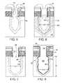
- FIG. 1is a sectional view illustrating a stage in a method of fabricating a trench capacitor in accordance with an embodiment of the invention.
- FIG. 2is a sectional view illustrating a stage in a method of fabricating a trench capacitor in accordance with an embodiment of the invention subsequent to the stage illustrated in FIG. 1 .
- FIG. 3Ais a sectional view illustrating a stage in a method of fabricating a trench capacitor in accordance with an embodiment of the invention subsequent to the stage illustrated in FIG. 2 .
- FIG. 3Bis an enlarged sectional view illustrating in detail a surface of a trench corresponding to the stage of fabrication shown in FIG. 3A .
- FIG. 4is a sectional view illustrating a stage in a method of fabricating a trench capacitor in accordance with an embodiment of the invention subsequent to the stage illustrated in FIG. 3 .
- FIG. 5is a sectional view illustrating a stage in a method of fabricating a trench capacitor in accordance with an embodiment of the invention subsequent to the stage illustrated in FIG. 4 .
- FIG. 6is a sectional view illustrating a stage in a method of fabricating a trench capacitor in accordance with an embodiment of the invention subsequent to the stage illustrated in FIG. 5 .
- FIG. 7is a sectional view illustrating a stage in a method of fabricating a trench capacitor in accordance with an embodiment of the invention subsequent to the stage illustrated in FIG. 6 .
- FIG. 8is a sectional view illustrating a stage in a method of fabricating a trench capacitor in accordance with an embodiment of the invention subsequent to the stage illustrated in FIG. 7 .
- FIG. 9Ais a sectional view illustrating a dynamic random access memory (“DRAM”) cell including a trench capacitor and a transistor having a vertically-oriented channel region, in accordance with an embodiment of the invention.
- DRAMdynamic random access memory
- FIG. 9Bis a sectional view illustrating DRAM cell including a trench capacitor and a transistor having a horizontally-oriented channel region, in accordance with an embodiment of the invention.
- FIG. 10is a sectional view illustrating a stage in a method of fabricating a trench capacitor in accordance with an embodiment of the invention.
- FIG. 11is a sectional view illustrating a stage in a method of fabricating a trench capacitor in accordance with an embodiment of the invention subsequent to the stage illustrated in FIG. 10 .
- FIG. 12is a sectional view illustrating a stage in a method of fabricating a trench capacitor in accordance with an embodiment of the invention subsequent to the stage illustrated in FIG. 1 .
- FIG. 13is a sectional view illustrating a stage in a method of fabricating a trench capacitor in accordance with an embodiment of the invention subsequent to the stage illustrated in FIG. 12 .
- FIG. 14is a sectional view illustrating a stage in a method of fabricating a trench capacitor in accordance with an embodiment of the invention subsequent to the stage illustrated in FIG. 13 .
- FIG. 15is a sectional view illustrating a stage in a method of fabricating a trench capacitor in accordance with an embodiment of the invention subsequent to the stage illustrated in FIG. 14 .
- FIG. 16is a sectional view illustrating a stage in a method of fabricating a trench capacitor in accordance with an embodiment of the invention subsequent to the stage illustrated in FIG. 15 .
- FIG. 17is a sectional view illustrating a stage in a method of fabricating a trench capacitor in accordance with an embodiment of the invention subsequent to the stage illustrated in FIG. 16 .
- FIG. 18is a sectional view illustrating a stage in a method of fabricating a trench capacitor in accordance with an embodiment of the invention subsequent to the stage illustrated in FIG. 17 .
- FIG. 19Ais a sectional view illustrating a DRAM cell including a trench capacitor and a transistor having a vertically-oriented channel region, in accordance with an embodiment of the invention.
- FIG. 19Bis a sectional view illustrating DRAM cell including a trench capacitor and a transistor having a horizontally-oriented channel region, in accordance with an embodiment of the invention.
- FIG. 1is a sectional view illustrating a stage in a method in accordance with an embodiment of the invention of fabricating a semiconductor chip containing a trench capacitor.
- a silicon-on-insulator (“SOI”) substrate 102includes a monocrystalline silicon layer (“SOI layer”) 104 separated from a bulk semiconductor layer 106 by a buried oxide (“BOX”) layer 108 .
- a pad dielectric layer 110 and a hard mask layer 112can be disposed atop the SOI substrate.
- the pad dielectric layer 110typically includes a pad layer of silicon nitride and may also include a pad layer of silicon oxide 110 A underlying the pad nitride.
- the hard mask layer 112typically includes a silicon oxide layer.
- the SOI layermay include other semiconductor materials, including but not limited to, germanium, silicon germanium, a compound semiconductor, such as a semiconductor material formed by a compound of a Group III element with a Group V element (gallium arsenide) or a compound of a Group II element with a Group VI element, or any combination of those materials.
- the SOI layer 104may have the same crystalline orientation as the semiconductor layer 106 or may have a different crystalline orientation.
- an openingis now formed which extends through the hard mask 112 , pad dielectric 110 , the silicon layer 104 and the BOX layer 108 to expose a surface of the bulk semiconductor region 106 underlying the BOX layer.
- the openingcan be formed by any suitable method such as lithography and a directional etch (e.g., reactive ion etch).
- a dielectric layer 114is formed which lines a wall 116 of the opening.
- the dielectric layer 114is formed by depositing silicon nitride onto the wall 116 of the opening and onto an exposed surface 118 of the hard mask layer 112 .
- the dielectric layer 114has walls 120 extending in a vertical direction 125 along the wall 116 of the silicon layer 104 and the dielectric layer has a bottom 122 extending in a direction transverse to the vertical direction.
- a reactive ion etch (“RIE”) processwhich includes ion bombardment, is performed, which forms an opening extending through the bottom 122 of the dielectric layer 114 and expose the underlying bulk semiconductor region 106 ( FIG. 3A ).
- RIEreactive ion etch
- vertically extending spacers 124are formed from the remains of the dielectric layer 114 ( FIG. 2 ) along the walls 116 .
- the same RIE processis continued to remove semiconductor material from the bulk semiconductor region 106 aligned with the opening in the dielectric layer to form a trench 126 .
- the ion bombardment during the RIE processresults in a wall 128 of the trench having much surface roughness, as particularly seen in the enlarged view of the wall 128 provided in FIG. 3B .
- the surface roughnesstypically ranges between about 1 nanometer and 10 nanometers root mean square (rms).
- an etch processis performed to etch the rough-surfaced wall of the trench 126 in a manner which depends upon the orientation of crystallographic planes within the bulk semiconductor region 106 .
- the crystallographic orientation-dependent etchcan be achieved by using a wet etch solution containing ammonia. As a result of such etch process; crystal facets 135 of the semiconductor material therein become exposed.
- the etch processcan enlarge the trench 126 from an initial lateral dimension 132 ( FIG. 3A ) after the initial RIE etch to a larger lateral dimension 134 . The remaining hard mask layer can be removed at this stage or later.
- the exposed crystal facetshave sharp edges and corners where the facets meet. If they were allowed to remain, the sharp edges and corners could be a source of problems in a capacitor formed along a surface of the wall 128 . High electric fields could result at the sharp edges and corners, leading to localized dielectric breakdown, and ultimately, increased leakage current and decreased reliability of the capacitor. Subsequent processing reduces, if not eliminates the sharp edges and corners before a capacitor dielectric layer is formed to extend along the wall 128 .
- a dopant source layer 136( FIG. 5 ) is formed to overlie the exposed wall 128 and spacer 124 .
- the dopant source layerincludes or consists at least essentially of doped oxide such as arsenic-doped silicate glass (“ASG”).
- ASGarsenic-doped silicate glass
- FIG. 6a dopant drive-in anneal is performed, in which the substrate with the dopant source layer thereon is heated to a high temperature sufficient to drive the dopant from the dopant source layer 136 into the bulk semiconductor region 106 adjacent thereto.
- the temperatureis similar to a temperature used to anneal the substrate following an ion implant step.
- an annealcan be performed at a temperature between about 750 and 1300° C. for a period of time between about 30 seconds and 30 minutes.
- a doped region 138is formed in the bulk semiconductor region 106 surrounding the dopant source layer 136 .
- the drive-in annealcan be performed in an environment containing a source of oxygen such as water vapor.
- a portion of the bulk semiconductor region adjacent to dopant source layer 136typically is oxidized to form an oxidized portion 140 .
- the lateral dimension 142 of the trenchis enlarged to an even greater extent than before.
- the resultis a trench 126 ′ having an enlarged lateral dimension 142 larger than the lateral dimension 134 ( FIG. 4 ) of the trench following the etch process illustrated therein.
- the wall 144 of the semiconductor region 106has a rough surface due to the exposed facets of the semiconductor region, but in which the sharp edges and corners between the facets of the semiconductor region have been smoothed into larger radius edges 146 and corners.
- the smoothed, larger radius edges 146 and cornersreduce the electric fields which could have occurred at those locations in the finished capacitor, than if the sharp edges and corners had remained in the finished capacitor.
- the surface roughnesstypically ranges between about 5 nanometers and 25 nanometers rms.
- the rounded corners and edges between facetshave a radius typically ranging between about 2 nanometers and 10 nanometers.
- stepsare performed to complete the trench capacitor 152 .
- the dielectric spacer 124( FIG. 7 ) on the wall 116 of the upper portion of the trench can be stripped and a node dielectric layer 148 then formed or deposited on the wall 116 and on the rough-surfaced wall 146 in the lower portion of the trench.
- an insulating layersuch as a dielectric collar 154 can be formed along a wall of the silicon layer 104 to avoid electrical interaction between the trench capacitor 152 and devices within the silicon layer 104 .
- Node dielectric layer 148may comprise any dielectric material appropriate for forming a trench capacitor, including but not limited to, silicon oxide, silicon nitride, silicon oxynitride, high-k material having a relative permittivity above about 8 , or any combination of these materials.
- high-k materialinclude but are not limited to hafnium oxide, hafnium silicon oxide, hafnium silicon oxynitride, aluminum oxide, zirconium oxide, and any combination of these materials.
- the node dielectric layer 148may be formed by any suitable method, including but not limited to, thermal oxidation, chemical oxidation, thermal nitridation, atomic layer deposition (ALD), molecular layer deposition (MLD), chemical vapor deposition (CVD), low-pressure chemical vapor deposition (LPCVD), and any combination of those methods.
- a conductive electrode material 150such as a doped polycrystalline semiconductor, a metal, a conductive compound of a metal (e.g., tungsten), a conductive metallic compound (e.g., titanium nitride), or a combination thereof can be deposited onto the node dielectric layer to form a node electrode.
- the node electrodecan fill the trench 126 ′ or the node electrode can line the node dielectric layer 148 along the wall 146 .
- the conductive electrode material 150may be formed by any suitable method, including but not limited to, atomic layer deposition (ALD), chemical vapor deposition (CVD), low-pressure chemical vapor deposition (LPCVD), and any combination of those methods.
- the wall 146provides a surface having greater surface area than that of a relatively smooth conventional trench wall.
- the trench capacitor 152can have significantly greater capacitance than a conventional trench capacitor.
- a capacitorcan be obtained which has a capacitance that is more than ten percent greater than that of a conventional trench capacitor having the same lateral dimension 142 and vertical length 151 .
- the increase in capacitance from the process described hereinmay be more than double the increase in capacitance that results from only enlarging the size of the trench using a bottle process.
- the trench capacitor 152can be connected to a transistor 156 having an active semiconductor region in the silicon layer 104 .
- the trench capacitorcan function as the capacitor of a dynamic random access memory (“DRAM”) cell 158 including the transistor 156 and trench capacitor 152 .
- DRAMdynamic random access memory
- the transistor 156can have a channel region 160 which is oriented in a vertical direction 125 with respect to the surface of the substrate 106 , the transistor being conductively connected to the node electrode 150 by way of a buried strap 162 and buried strap outdiffusion 164 .
- the trench capacitor 152can be connected to a planar transistor 166 of a DRAM cell 168 , in which the transistor has a channel region 170 oriented in a horizontal direction 172 with respect to the surface of the substrate 106 .
- the transistorcan be conductively connected to the node electrode 150 by way of a buried strap outdiffusion 174 .
- the transistors shown in FIGS. 9A-Bare merely illustrative of a great variety of transistor structures and DRAM cell designs which can be fabricated to connect with and operate cooperatively with the trench capacitor shown therein.
- FIG. 10varies with respect to FIG. 1 in that the substrate 202 in FIG. 10 is a bulk monocrystalline semiconductor region rather than a silicon-on-insulator structure as shown in FIG. 10 which has a buried oxide layer. As illustrated in FIG. 11 , an opening is formed in the hard mask layer 212 and underlying pad dielectric layer 210 , upon a wall of which a dielectric layer 214 then is formed.
- FIGS. 12 through 17are the same as those described above with reference to FIGS. 3 to 7 .
- a trench 226( FIG. 12 ) is formed in the bulk semiconductor region 206 below the dielectric spacer 224 , the trench having a wall 228 with a rough surface. The rough surface wall then is etched to expose the ⁇ 111> facets 235 of the semiconductor crystal as shown in FIG. 13 .
- FIG. 14illustrates a stage of fabrication in which a dopant source layer 236 is formed on a wall 228 of the semiconductor region 206 .
- FIG. 15illustrates a stage after annealing to drive a dopant contained in the dopant source layer 236 into the semiconductor region 206 to form a buried plate doped region 238 and oxidize a portion of the semiconductor region 206 adjacent to the wall 228 to form an oxide layer 240 .
- FIG. 16illustrates a stage of fabrication after the dopant source layer and oxide layer have been removed to expose the faceted wall 246 of the semiconductor region. With the removal of the oxide layer, the corners and edges between the facets become more rounded, i.e., they have larger radius, such as described above with respect to FIG. 7 .
- FIG. 17illustrates a stage of fabrication after forming a node dielectric 248 in contact with the exposed faceted wall 246 and a node electrode 250 is formed. As shown in FIG. 17 , optionally the dielectric spacer 224 can be left in place as a dielectric collar.
- FIG. 18shows a stage of fabrication after the spacer, node dielectric 248 and node electrode 250 thereon are recessed to form a collar 260 below an exposed transistor region 262 of the semiconductor region 206 .
- a transistor 256can be formed which has a vertically-oriented channel region in the transistor region 262 of the substrate and having a conductive connection to the node electrode 250 of the trench capacitor.
- the trench capacitorcan function as the capacitor of a dynamic random access memory (“DRAM”) cell 258 including the transistor 256 and trench capacitor 252 .
- DRAMdynamic random access memory
- the trench capacitor 252can be connected to a planar transistor 266 of a DRAM cell 268 , in which the transistor has a channel region 270 oriented in a horizontal direction 272 with respect to the surface of the substrate 206 .
- the transistors shown in FIGS. 19A-Bare merely illustrative of a great variety of transistor structures and DRAM cell designs which can be fabricated to connect with and operate cooperatively with the trench capacitor shown therein.
Landscapes
- Engineering & Computer Science (AREA)
- Manufacturing & Machinery (AREA)
- Semiconductor Memories (AREA)
- Semiconductor Integrated Circuits (AREA)
Abstract
Description
- 1. Field of the Invention
- The present invention relates to semiconductor devices and their manufacture, and more specifically to a structure and method of making a semiconductor chip having a trench capacitor.
- 2. Description of the Related Art
- One of the challenges of fabricating capacitors within the active device regions of semiconductor chips is to obtain sufficient capacitance while minimizing the area of the active semiconductor device layer occupied by the capacitor. One known way to reduce the semiconductor device area occupied by the capacitor is to use a trench capacitor. A trench capacitor has length extending in a vertically downward direction with respect to the semiconductor device layer, so that the long dimension of the trench capacitor extends out of the plane in which the semiconductor device layer extends.
- A known way of increasing capacitance is to form the trench capacitor using a “bottle” process. In such process, first a relatively narrow trench is formed that extends through the active semiconductor device layer. Then, subsequent processing applied to a lower portion of the trench underlying the active semiconductor device layer to enlarge the lower portion of the trench, thus forming a capacitor having a larger surface area and capacitance.
- Still further improvements in the fabrication and structure of a trench capacitor would be desirable.
- In accordance with an aspect of the invention, a method is provided for fabricating a semiconductor chip including a trench capacitor. In such method, a monocrystalline semiconductor region can be etched in a vertical direction through an opening in a dielectric layer to form a trench having a rough-surfaced wall of exposed semiconductor material. The trench has an initial lateral dimension in a first direction transverse to the vertical direction. The rough-surfaced wall of the trench then is etched in a crystallographic orientation-dependent manner to expose a multiplicity of crystal facets of the semiconductor region at the trench wall. A dopant-containing liner may then be deposited to line the wall of the trench and a temperature of the substrate then be elevated to drive a dopant from the dopant-containing liner into the semiconductor region adjacent to the trench wall. During such step, typically a portion of the semiconductor material exposed at the trench wall is oxidized.
- Subsequently, the dopant-containing liner and at least some of the oxidized portion of the semiconductor material can be removed to expose a wall of an enlarged trench within the semiconductor region. The enlarged trench can have an enlarged lateral dimension relative to the initial lateral dimension. The enlarged trench can have a roughness in accordance with the multiplicity of crystal facets, and have smoothed edges which correspond to the boundaries between the crystal facets. The oxidation of the semiconductor region and removal of the oxide layer therefrom has an effect of smoothing sharp edges and corners at boundaries between the crystal facets. A node dielectric layer can then be formed adjacent to the surface of the enlarged trench and a layer of conductive material be formed adjacent to the node dielectric layer to form a trench capacitor.
- In accordance with a particular aspect of the invention, the semiconductor region can be a bulk semiconductor region of a substrate and the substrate can include a monocrystalline silicon layer and a buried oxide (“BOX”) region separating the silicon layer from the bulk semiconductor region. The process of etching the monocrystalline silicon region can include etching an opening in the silicon layer and the BOX region and forming a dielectric layer lining a wall of the opening.
- In accordance with another aspect of the invention, a semiconductor chip is provided which includes a trench capacitor. In accordance with such aspect, a trench can extend within a monocrystalline semiconductor region and have an enlarged lateral dimension relative to a lateral dimension of the trench at a mouth of the trench. The trench can have a rough surface in accordance with a multiplicity of crystal facets exposed at the surface, the surface also having smoothed edges at boundaries between the crystal facets. A node dielectric layer of the trench capacitor can be disposed adjacent to the surface of the enlarged trench and a layer of conductive material adjacent to the node dielectric layer.
FIG. 1 is a sectional view illustrating a stage in a method of fabricating a trench capacitor in accordance with an embodiment of the invention.FIG. 2 is a sectional view illustrating a stage in a method of fabricating a trench capacitor in accordance with an embodiment of the invention subsequent to the stage illustrated inFIG. 1 .FIG. 3A is a sectional view illustrating a stage in a method of fabricating a trench capacitor in accordance with an embodiment of the invention subsequent to the stage illustrated inFIG. 2 .FIG. 3B is an enlarged sectional view illustrating in detail a surface of a trench corresponding to the stage of fabrication shown inFIG. 3A .FIG. 4 is a sectional view illustrating a stage in a method of fabricating a trench capacitor in accordance with an embodiment of the invention subsequent to the stage illustrated inFIG. 3 .FIG. 5 is a sectional view illustrating a stage in a method of fabricating a trench capacitor in accordance with an embodiment of the invention subsequent to the stage illustrated inFIG. 4 .FIG. 6 is a sectional view illustrating a stage in a method of fabricating a trench capacitor in accordance with an embodiment of the invention subsequent to the stage illustrated inFIG. 5 .FIG. 7 is a sectional view illustrating a stage in a method of fabricating a trench capacitor in accordance with an embodiment of the invention subsequent to the stage illustrated inFIG. 6 .FIG. 8 is a sectional view illustrating a stage in a method of fabricating a trench capacitor in accordance with an embodiment of the invention subsequent to the stage illustrated inFIG. 7 .FIG. 9A is a sectional view illustrating a dynamic random access memory (“DRAM”) cell including a trench capacitor and a transistor having a vertically-oriented channel region, in accordance with an embodiment of the invention.FIG. 9B is a sectional view illustrating DRAM cell including a trench capacitor and a transistor having a horizontally-oriented channel region, in accordance with an embodiment of the invention.FIG. 10 is a sectional view illustrating a stage in a method of fabricating a trench capacitor in accordance with an embodiment of the invention.FIG. 11 is a sectional view illustrating a stage in a method of fabricating a trench capacitor in accordance with an embodiment of the invention subsequent to the stage illustrated inFIG. 10 .FIG. 12 is a sectional view illustrating a stage in a method of fabricating a trench capacitor in accordance with an embodiment of the invention subsequent to the stage illustrated inFIG. 1 .FIG. 13 is a sectional view illustrating a stage in a method of fabricating a trench capacitor in accordance with an embodiment of the invention subsequent to the stage illustrated inFIG. 12 .FIG. 14 is a sectional view illustrating a stage in a method of fabricating a trench capacitor in accordance with an embodiment of the invention subsequent to the stage illustrated inFIG. 13 .FIG. 15 is a sectional view illustrating a stage in a method of fabricating a trench capacitor in accordance with an embodiment of the invention subsequent to the stage illustrated inFIG. 14 .FIG. 16 is a sectional view illustrating a stage in a method of fabricating a trench capacitor in accordance with an embodiment of the invention subsequent to the stage illustrated inFIG. 15 .FIG. 17 is a sectional view illustrating a stage in a method of fabricating a trench capacitor in accordance with an embodiment of the invention subsequent to the stage illustrated inFIG. 16 .FIG. 18 is a sectional view illustrating a stage in a method of fabricating a trench capacitor in accordance with an embodiment of the invention subsequent to the stage illustrated inFIG. 17 .FIG. 19A is a sectional view illustrating a DRAM cell including a trench capacitor and a transistor having a vertically-oriented channel region, in accordance with an embodiment of the invention.FIG. 19B is a sectional view illustrating DRAM cell including a trench capacitor and a transistor having a horizontally-oriented channel region, in accordance with an embodiment of the invention.FIG. 1 is a sectional view illustrating a stage in a method in accordance with an embodiment of the invention of fabricating a semiconductor chip containing a trench capacitor. As illustrated inFIG. 1 , a silicon-on-insulator (“SOI”)substrate 102 includes a monocrystalline silicon layer (“SOI layer”)104 separated from abulk semiconductor layer 106 by a buried oxide (“BOX”)layer 108. A paddielectric layer 110 and ahard mask layer 112 can be disposed atop the SOI substrate. Thepad dielectric layer 110 typically includes a pad layer of silicon nitride and may also include a pad layer ofsilicon oxide 110A underlying the pad nitride. Thehard mask layer 112 typically includes a silicon oxide layer. Besides silicon, the SOI layer may include other semiconductor materials, including but not limited to, germanium, silicon germanium, a compound semiconductor, such as a semiconductor material formed by a compound of a Group III element with a Group V element (gallium arsenide) or a compound of a Group II element with a Group VI element, or any combination of those materials. TheSOI layer 104 may have the same crystalline orientation as thesemiconductor layer 106 or may have a different crystalline orientation.- As illustrated in
FIG. 2 , an opening is now formed which extends through thehard mask 112,pad dielectric 110, thesilicon layer 104 and theBOX layer 108 to expose a surface of thebulk semiconductor region 106 underlying the BOX layer. The opening can be formed by any suitable method such as lithography and a directional etch (e.g., reactive ion etch). Adielectric layer 114 is formed which lines awall 116 of the opening. In one embodiment, thedielectric layer 114 is formed by depositing silicon nitride onto thewall 116 of the opening and onto an exposedsurface 118 of thehard mask layer 112. As seen inFIG. 2 , thedielectric layer 114 haswalls 120 extending in avertical direction 125 along thewall 116 of thesilicon layer 104 and the dielectric layer has a bottom122 extending in a direction transverse to the vertical direction. - Subsequently, a reactive ion etch (“RIE”) process, which includes ion bombardment, is performed, which forms an opening extending through the
bottom 122 of thedielectric layer 114 and expose the underlying bulk semiconductor region106 (FIG. 3A ). As a result, vertically extendingspacers 124 are formed from the remains of the dielectric layer114 (FIG. 2 ) along thewalls 116. The same RIE process is continued to remove semiconductor material from thebulk semiconductor region 106 aligned with the opening in the dielectric layer to form atrench 126. The ion bombardment during the RIE process results in awall 128 of the trench having much surface roughness, as particularly seen in the enlarged view of thewall 128 provided inFIG. 3B . At this stage of fabrication, the surface roughness typically ranges between about 1 nanometer and 10 nanometers root mean square (rms). - Thereafter, as illustrated in
FIG. 4 , an etch process is performed to etch the rough-surfaced wall of thetrench 126 in a manner which depends upon the orientation of crystallographic planes within thebulk semiconductor region 106. For example, the crystallographic orientation-dependent etch can be achieved by using a wet etch solution containing ammonia. As a result of such etch process;crystal facets 135 of the semiconductor material therein become exposed. In addition, the etch process can enlarge thetrench 126 from an initial lateral dimension132 (FIG. 3A ) after the initial RIE etch to a largerlateral dimension 134. The remaining hard mask layer can be removed at this stage or later. - In a
semiconductor substrate 102 in which amajor surface 130 of thebulk semiconductor region 106 is in the <100> crystal orientation, the etch process exposes a multiplicity ofcrystal facets 135 of thebulk semiconductor region 106, such asfacets 135 in the <111> crystallographic orientation. With an etch process highly dependent upon the crystallographic plane of the material, etching stops oncefacets 135 aligned with the <111> plane of the crystal become exposed. - However, the exposed crystal facets have sharp edges and corners where the facets meet. If they were allowed to remain, the sharp edges and corners could be a source of problems in a capacitor formed along a surface of the
wall 128. High electric fields could result at the sharp edges and corners, leading to localized dielectric breakdown, and ultimately, increased leakage current and decreased reliability of the capacitor. Subsequent processing reduces, if not eliminates the sharp edges and corners before a capacitor dielectric layer is formed to extend along thewall 128. - Subsequently, a dopant source layer136 (
FIG. 5 ) is formed to overlie the exposedwall 128 andspacer 124. Typically, the dopant source layer includes or consists at least essentially of doped oxide such as arsenic-doped silicate glass (“ASG”). As illustrated inFIG. 6 , a dopant drive-in anneal is performed, in which the substrate with the dopant source layer thereon is heated to a high temperature sufficient to drive the dopant from thedopant source layer 136 into thebulk semiconductor region 106 adjacent thereto. Typically, the temperature is similar to a temperature used to anneal the substrate following an ion implant step. For example, an anneal can be performed at a temperature between about 750 and 1300° C. for a period of time between about30 seconds and 30 minutes. As a result, a dopedregion 138 is formed in thebulk semiconductor region 106 surrounding thedopant source layer 136. In addition, the drive-in anneal can be performed in an environment containing a source of oxygen such as water vapor. As a result, a portion of the bulk semiconductor region adjacent to dopantsource layer 136 typically is oxidized to form an oxidizedportion 140. - Because a portion of the bulk semiconductor region is oxidized and consumed during oxidation, the
lateral dimension 142 of the trench is enlarged to an even greater extent than before. The sharp edges and corners, where the crystal facets of the wall meet, oxidize faster than the flat facets between the edges and corners. As a result, the sharp edges and corners are consumed by oxide and become larger radius edges146 and corners. - As seen in
FIG. 7 , a process now is performed to remove the oxidizedportion 140 of thesemiconductor region 106 from overlying the buried plate dopedregion 138, and with it, the dopant source layer as well, for example, by a wet etch solution containing hydrofluoric acid. The result is atrench 126′ having an enlargedlateral dimension 142 larger than the lateral dimension134 (FIG. 4 ) of the trench following the etch process illustrated therein. Thewall 144 of thesemiconductor region 106 has a rough surface due to the exposed facets of the semiconductor region, but in which the sharp edges and corners between the facets of the semiconductor region have been smoothed into larger radius edges146 and corners. The smoothed, larger radius edges146 and corners reduce the electric fields which could have occurred at those locations in the finished capacitor, than if the sharp edges and corners had remained in the finished capacitor. Once this stage of fabrication is reached, the surface roughness typically ranges between about 5 nanometers and 25 nanometers rms. The rounded corners and edges between facets have a radius typically ranging between about 2 nanometers and 10 nanometers. - As seen in
FIG. 8 , steps are performed to complete thetrench capacitor 152. The dielectric spacer124 (FIG. 7 ) on thewall 116 of the upper portion of the trench can be stripped and anode dielectric layer 148 then formed or deposited on thewall 116 and on the rough-surfacedwall 146 in the lower portion of the trench. After stripping thedielectric spacer 124, optionally, an insulating layer such as adielectric collar 154 can be formed along a wall of thesilicon layer 104 to avoid electrical interaction between thetrench capacitor 152 and devices within thesilicon layer 104.Node dielectric layer 148 may comprise any dielectric material appropriate for forming a trench capacitor, including but not limited to, silicon oxide, silicon nitride, silicon oxynitride, high-k material having a relative permittivity above about8, or any combination of these materials. Examples of high-k material include but are not limited to hafnium oxide, hafnium silicon oxide, hafnium silicon oxynitride, aluminum oxide, zirconium oxide, and any combination of these materials. Thenode dielectric layer 148 may be formed by any suitable method, including but not limited to, thermal oxidation, chemical oxidation, thermal nitridation, atomic layer deposition (ALD), molecular layer deposition (MLD), chemical vapor deposition (CVD), low-pressure chemical vapor deposition (LPCVD), and any combination of those methods. - Subsequently, a
conductive electrode material 150 such as a doped polycrystalline semiconductor, a metal, a conductive compound of a metal (e.g., tungsten), a conductive metallic compound (e.g., titanium nitride), or a combination thereof can be deposited onto the node dielectric layer to form a node electrode. The node electrode can fill thetrench 126′ or the node electrode can line thenode dielectric layer 148 along thewall 146. Theconductive electrode material 150 may be formed by any suitable method, including but not limited to, atomic layer deposition (ALD), chemical vapor deposition (CVD), low-pressure chemical vapor deposition (LPCVD), and any combination of those methods. - Because the node dielectric layer is formed on a
wall 146 of the trench having exposed facets, thewall 146 provides a surface having greater surface area than that of a relatively smooth conventional trench wall. As a result, thetrench capacitor 152 can have significantly greater capacitance than a conventional trench capacitor. For example, a capacitor can be obtained which has a capacitance that is more than ten percent greater than that of a conventional trench capacitor having the samelateral dimension 142 andvertical length 151. For example, the increase in capacitance from the process described herein may be more than double the increase in capacitance that results from only enlarging the size of the trench using a bottle process. - Alternatively, as illustrated in
FIG. 9A , thetrench capacitor 152 can be connected to atransistor 156 having an active semiconductor region in thesilicon layer 104. In this way, the trench capacitor can function as the capacitor of a dynamic random access memory (“DRAM”)cell 158 including thetransistor 156 andtrench capacitor 152. In the embodiment seen inFIG. 9 , thetransistor 156 can have achannel region 160 which is oriented in avertical direction 125 with respect to the surface of thesubstrate 106, the transistor being conductively connected to thenode electrode 150 by way of a buriedstrap 162 and buriedstrap outdiffusion 164. - In another variation, as illustrated in
FIG. 9B , thetrench capacitor 152 can be connected to aplanar transistor 166 of aDRAM cell 168, in which the transistor has a channel region170 oriented in ahorizontal direction 172 with respect to the surface of thesubstrate 106. In this case, the transistor can be conductively connected to thenode electrode 150 by way of a buriedstrap outdiffusion 174. The transistors shown inFIGS. 9A-B are merely illustrative of a great variety of transistor structures and DRAM cell designs which can be fabricated to connect with and operate cooperatively with the trench capacitor shown therein. - A variation of the embodiment of the invention illustrated in
FIGS. 1-9B will now be described.FIG. 10 illustrates amonocrystalline semiconductor substrate 202 in an initial stage of fabrication, the substrate having apad dielectric layer 210 thereon and ahard mask layer 212 overlying the pad dielectric layer. The pad dielectric layer may include a layer of silicon nitride overlying a layer of silicon oxide adjacent to the semiconductor substrate, for example FIG. 10 varies with respect toFIG. 1 in that thesubstrate 202 inFIG. 10 is a bulk monocrystalline semiconductor region rather than a silicon-on-insulator structure as shown inFIG. 10 which has a buried oxide layer. As illustrated inFIG. 11 , an opening is formed in thehard mask layer 212 and underlyingpad dielectric layer 210, upon a wall of which a dielectric layer214 then is formed.- Except for the lack of a BOX layer and an overlying monocrystalline silicon layer in the substrate overlying the
bulk semiconductor region 206, the subsequent series of processing steps illustrated with reference toFIGS. 12 through 17 are the same as those described above with reference toFIGS. 3 to 7 . Thus, a trench226 (FIG. 12 ) is formed in thebulk semiconductor region 206 below thedielectric spacer 224, the trench having awall 228 with a rough surface. The rough surface wall then is etched to expose the <111>facets 235 of the semiconductor crystal as shown inFIG. 13 .FIG. 14 illustrates a stage of fabrication in which adopant source layer 236 is formed on awall 228 of thesemiconductor region 206.FIG. 15 illustrates a stage after annealing to drive a dopant contained in thedopant source layer 236 into thesemiconductor region 206 to form a buried plate dopedregion 238 and oxidize a portion of thesemiconductor region 206 adjacent to thewall 228 to form anoxide layer 240. FIG. 16 illustrates a stage of fabrication after the dopant source layer and oxide layer have been removed to expose thefaceted wall 246 of the semiconductor region. With the removal of the oxide layer, the corners and edges between the facets become more rounded, i.e., they have larger radius, such as described above with respect toFIG. 7 .FIG. 17 illustrates a stage of fabrication after forming anode dielectric 248 in contact with the exposedfaceted wall 246 and anode electrode 250 is formed. As shown inFIG. 17 , optionally thedielectric spacer 224 can be left in place as a dielectric collar.FIG. 18 shows a stage of fabrication after the spacer,node dielectric 248 andnode electrode 250 thereon are recessed to form acollar 260 below an exposedtransistor region 262 of thesemiconductor region 206.- Subsequently, as illustrated in
FIG. 19A , atransistor 256 can be formed which has a vertically-oriented channel region in thetransistor region 262 of the substrate and having a conductive connection to thenode electrode 250 of the trench capacitor. Again, the trench capacitor can function as the capacitor of a dynamic random access memory (“DRAM”)cell 258 including thetransistor 256 andtrench capacitor 252. - In another variation, as illustrated in
FIG. 19B , thetrench capacitor 252 can be connected to aplanar transistor 266 of aDRAM cell 268, in which the transistor has achannel region 270 oriented in ahorizontal direction 272 with respect to the surface of thesubstrate 206. The transistors shown inFIGS. 19A-B are merely illustrative of a great variety of transistor structures and DRAM cell designs which can be fabricated to connect with and operate cooperatively with the trench capacitor shown therein. - While the invention has been described in accordance with certain preferred embodiments thereof, those skilled in the art will understand the many modifications and enhancements which can be made thereto without departing from the true scope and spirit of the invention, which is limited only by the claims appended below.
Claims (20)
Priority Applications (1)
| Application Number | Priority Date | Filing Date | Title |
|---|---|---|---|
| US12/423,242US8021945B2 (en) | 2009-04-14 | 2009-04-14 | Bottle-shaped trench capacitor with enhanced capacitance |
Applications Claiming Priority (1)
| Application Number | Priority Date | Filing Date | Title |
|---|---|---|---|
| US12/423,242US8021945B2 (en) | 2009-04-14 | 2009-04-14 | Bottle-shaped trench capacitor with enhanced capacitance |
Publications (2)
| Publication Number | Publication Date |
|---|---|
| US20100258904A1true US20100258904A1 (en) | 2010-10-14 |
| US8021945B2 US8021945B2 (en) | 2011-09-20 |
Family
ID=42933711
Family Applications (1)
| Application Number | Title | Priority Date | Filing Date |
|---|---|---|---|
| US12/423,242Expired - Fee RelatedUS8021945B2 (en) | 2009-04-14 | 2009-04-14 | Bottle-shaped trench capacitor with enhanced capacitance |
Country Status (1)
| Country | Link |
|---|---|
| US (1) | US8021945B2 (en) |
Cited By (6)
| Publication number | Priority date | Publication date | Assignee | Title |
|---|---|---|---|---|
| US20110108916A1 (en)* | 2009-11-06 | 2011-05-12 | Infineon Technologies Ag | Semiconductor Devices and Methods |
| WO2012106720A1 (en)* | 2011-02-04 | 2012-08-09 | Qualcomm Incorporated | High density metal-insulator-metal trench capacitor with concave surfaces |
| GB2497201A (en)* | 2011-11-30 | 2013-06-05 | Ibm | A low resistance embedded strap for a trench capacitor |
| US20140048917A1 (en)* | 2010-01-18 | 2014-02-20 | Semiconductor Components Industries, Llc | Em protected semiconductor die |
| US20170186837A1 (en)* | 2015-12-29 | 2017-06-29 | Taiwan Semiconductor Manufacturing Co., Ltd. | Deep trench capacitor with scallop profile |
| DE102016122943B4 (en) | 2015-12-29 | 2024-03-21 | Taiwan Semiconductor Manufacturing Co., Ltd. | INTEGRATED CHIP INCLUDING A DEEP TRENCH CAPACITOR WITH A CORRUPTED PROFILE AND MANUFACTURING PROCESS FOR THE LATTER |
Families Citing this family (1)
| Publication number | Priority date | Publication date | Assignee | Title |
|---|---|---|---|---|
| US8227311B2 (en) | 2010-10-07 | 2012-07-24 | International Business Machines Corporation | Method of forming enhanced capacitance trench capacitor |
Citations (30)
| Publication number | Priority date | Publication date | Assignee | Title |
|---|---|---|---|---|
| US6025225A (en)* | 1998-01-22 | 2000-02-15 | Micron Technology, Inc. | Circuits with a trench capacitor having micro-roughened semiconductor surfaces and methods for forming the same |
| US6037620A (en)* | 1998-06-08 | 2000-03-14 | International Business Machines Corporation | DRAM cell with transfer device extending along perimeter of trench storage capacitor |
| US6153474A (en)* | 1996-03-04 | 2000-11-28 | International Business Machines Corporation | Method of controllably forming a LOCOS oxide layer over a portion of a vertically extending sidewall of a trench extending into a semiconductor substrate |
| US6171872B1 (en)* | 1996-01-29 | 2001-01-09 | Micron Technology, Inc. | Method of monitoring a process of manufacturing a semiconductor wafer including hemispherical grain polysilicon |
| US6177696B1 (en)* | 1998-08-13 | 2001-01-23 | International Business Machines Corporation | Integration scheme enhancing deep trench capacitance in semiconductor integrated circuit devices |
| US6190988B1 (en)* | 1998-05-28 | 2001-02-20 | International Business Machines Corporation | Method for a controlled bottle trench for a dram storage node |
| US6200873B1 (en)* | 1998-09-17 | 2001-03-13 | Siemens Aktiengesellschaft | Production method for a trench capacitor with an insulation collar |
| US6232171B1 (en)* | 1999-01-11 | 2001-05-15 | Promos Technology, Inc. | Technique of bottle-shaped deep trench formation |
| US6271079B1 (en)* | 1999-05-07 | 2001-08-07 | Mosel Vitelic Inc. | Method of forming a trench capacitor |
| US6291289B2 (en)* | 1999-06-25 | 2001-09-18 | Micron Technology, Inc. | Method of forming DRAM trench capacitor with metal layer over hemispherical grain polysilicon |
| US6365485B1 (en)* | 2000-04-19 | 2002-04-02 | Promos Tech., Inc, | DRAM technology of buried plate formation of bottle-shaped deep trench |
| US6391712B2 (en)* | 2000-08-11 | 2002-05-21 | Hynix Semiconductor, Inc. | Method of forming a storage node of a capacitor that prevents HSG(Hemi-Spherical Grain) bridging |
| US6440792B1 (en)* | 1999-11-05 | 2002-08-27 | Promos Technology, Inc. | DRAM technology of storage node formation and no conduction/isolation process of bottle-shaped deep trench |
| US6448131B1 (en)* | 2001-08-14 | 2002-09-10 | International Business Machines Corporation | Method for increasing the capacitance of a trench capacitor |
| US6555430B1 (en)* | 2000-11-28 | 2003-04-29 | International Business Machines Corporation | Process flow for capacitance enhancement in a DRAM trench |
| US6566177B1 (en)* | 1999-10-25 | 2003-05-20 | International Business Machines Corporation | Silicon-on-insulator vertical array device trench capacitor DRAM |
| US6713341B2 (en)* | 2002-02-05 | 2004-03-30 | Nanya Technology Corporation | Method of forming a bottle-shaped trench in a semiconductor substrate |
| US6806138B1 (en)* | 2004-01-21 | 2004-10-19 | International Business Machines Corporation | Integration scheme for enhancing capacitance of trench capacitors |
| US6828191B1 (en)* | 1998-06-15 | 2004-12-07 | Siemens Aktiengesellschaft | Trench capacitor with an insulation collar and method for producing a trench capacitor |
| US6846744B1 (en)* | 2003-10-17 | 2005-01-25 | Nanya Technology Corp. | Method of fabricating a bottle shaped deep trench for trench capacitor DRAM devices |
| US6849529B2 (en)* | 2002-10-25 | 2005-02-01 | Promos Technologies Inc. | Deep-trench capacitor with hemispherical grain silicon surface and method for making the same |
| US6867089B2 (en)* | 2002-01-28 | 2005-03-15 | Nanya Technology Corporation | Method of forming a bottle-shaped trench in a semiconductor substrate |
| US6872621B1 (en)* | 2003-11-06 | 2005-03-29 | Promos Technologies Inc. | Method for removal of hemispherical grained silicon in a deep trench |
| US6977227B2 (en)* | 2004-03-18 | 2005-12-20 | Nanya Technology Corporation | Method of etching bottle trench and fabricating capacitor with same |
| US6989561B2 (en)* | 2003-12-02 | 2006-01-24 | Nanya Technology Corp. | Trench capacitor structure |
| US7101768B2 (en)* | 2002-09-27 | 2006-09-05 | International Business Machines Corporation | Self-aligned selective hemispherical grain deposition process and structure for enhanced capacitance trench capacitor |
| US7112505B2 (en)* | 2003-11-25 | 2006-09-26 | Promos Technologies, Inc. | Method of selectively etching HSG layer in deep trench capacitor fabrication |
| US7115934B2 (en)* | 2004-03-26 | 2006-10-03 | International Business Machines Corporation | Method and structure for enhancing trench capacitance |
| US20060228864A1 (en)* | 2005-04-12 | 2006-10-12 | Promos Technologies Inc. | Semiconductor devices having a bottle-shaped deep trench capacitor and methods for making the same using Epi-Si growth process |
| US7122439B2 (en)* | 2004-11-17 | 2006-10-17 | International Business Machines Corporation | Method of fabricating a bottle trench and a bottle trench capacitor |
- 2009
- 2009-04-14USUS12/423,242patent/US8021945B2/ennot_activeExpired - Fee Related
Patent Citations (32)
| Publication number | Priority date | Publication date | Assignee | Title |
|---|---|---|---|---|
| US6171872B1 (en)* | 1996-01-29 | 2001-01-09 | Micron Technology, Inc. | Method of monitoring a process of manufacturing a semiconductor wafer including hemispherical grain polysilicon |
| US6153474A (en)* | 1996-03-04 | 2000-11-28 | International Business Machines Corporation | Method of controllably forming a LOCOS oxide layer over a portion of a vertically extending sidewall of a trench extending into a semiconductor substrate |
| US6025225A (en)* | 1998-01-22 | 2000-02-15 | Micron Technology, Inc. | Circuits with a trench capacitor having micro-roughened semiconductor surfaces and methods for forming the same |
| US7084451B2 (en)* | 1998-01-22 | 2006-08-01 | Micron Technology, Inc. | Circuits with a trench capacitor having micro-roughened semiconductor surfaces |
| US6190988B1 (en)* | 1998-05-28 | 2001-02-20 | International Business Machines Corporation | Method for a controlled bottle trench for a dram storage node |
| US6037620A (en)* | 1998-06-08 | 2000-03-14 | International Business Machines Corporation | DRAM cell with transfer device extending along perimeter of trench storage capacitor |
| US6828191B1 (en)* | 1998-06-15 | 2004-12-07 | Siemens Aktiengesellschaft | Trench capacitor with an insulation collar and method for producing a trench capacitor |
| US6177696B1 (en)* | 1998-08-13 | 2001-01-23 | International Business Machines Corporation | Integration scheme enhancing deep trench capacitance in semiconductor integrated circuit devices |
| US6200873B1 (en)* | 1998-09-17 | 2001-03-13 | Siemens Aktiengesellschaft | Production method for a trench capacitor with an insulation collar |
| US6232171B1 (en)* | 1999-01-11 | 2001-05-15 | Promos Technology, Inc. | Technique of bottle-shaped deep trench formation |
| US6271079B1 (en)* | 1999-05-07 | 2001-08-07 | Mosel Vitelic Inc. | Method of forming a trench capacitor |
| US6291289B2 (en)* | 1999-06-25 | 2001-09-18 | Micron Technology, Inc. | Method of forming DRAM trench capacitor with metal layer over hemispherical grain polysilicon |
| US6566177B1 (en)* | 1999-10-25 | 2003-05-20 | International Business Machines Corporation | Silicon-on-insulator vertical array device trench capacitor DRAM |
| US6440792B1 (en)* | 1999-11-05 | 2002-08-27 | Promos Technology, Inc. | DRAM technology of storage node formation and no conduction/isolation process of bottle-shaped deep trench |
| US6365485B1 (en)* | 2000-04-19 | 2002-04-02 | Promos Tech., Inc, | DRAM technology of buried plate formation of bottle-shaped deep trench |
| US6391712B2 (en)* | 2000-08-11 | 2002-05-21 | Hynix Semiconductor, Inc. | Method of forming a storage node of a capacitor that prevents HSG(Hemi-Spherical Grain) bridging |
| US6555430B1 (en)* | 2000-11-28 | 2003-04-29 | International Business Machines Corporation | Process flow for capacitance enhancement in a DRAM trench |
| US6448131B1 (en)* | 2001-08-14 | 2002-09-10 | International Business Machines Corporation | Method for increasing the capacitance of a trench capacitor |
| US6867089B2 (en)* | 2002-01-28 | 2005-03-15 | Nanya Technology Corporation | Method of forming a bottle-shaped trench in a semiconductor substrate |
| US6713341B2 (en)* | 2002-02-05 | 2004-03-30 | Nanya Technology Corporation | Method of forming a bottle-shaped trench in a semiconductor substrate |
| US7101768B2 (en)* | 2002-09-27 | 2006-09-05 | International Business Machines Corporation | Self-aligned selective hemispherical grain deposition process and structure for enhanced capacitance trench capacitor |
| US6849529B2 (en)* | 2002-10-25 | 2005-02-01 | Promos Technologies Inc. | Deep-trench capacitor with hemispherical grain silicon surface and method for making the same |
| US7009238B2 (en)* | 2002-10-25 | 2006-03-07 | Promos Technologies Inc. | Deep-trench capacitor with hemispherical grain silicon surface and method for making the same |
| US6846744B1 (en)* | 2003-10-17 | 2005-01-25 | Nanya Technology Corp. | Method of fabricating a bottle shaped deep trench for trench capacitor DRAM devices |
| US6872621B1 (en)* | 2003-11-06 | 2005-03-29 | Promos Technologies Inc. | Method for removal of hemispherical grained silicon in a deep trench |
| US7112505B2 (en)* | 2003-11-25 | 2006-09-26 | Promos Technologies, Inc. | Method of selectively etching HSG layer in deep trench capacitor fabrication |
| US6989561B2 (en)* | 2003-12-02 | 2006-01-24 | Nanya Technology Corp. | Trench capacitor structure |
| US6806138B1 (en)* | 2004-01-21 | 2004-10-19 | International Business Machines Corporation | Integration scheme for enhancing capacitance of trench capacitors |
| US6977227B2 (en)* | 2004-03-18 | 2005-12-20 | Nanya Technology Corporation | Method of etching bottle trench and fabricating capacitor with same |
| US7115934B2 (en)* | 2004-03-26 | 2006-10-03 | International Business Machines Corporation | Method and structure for enhancing trench capacitance |
| US7122439B2 (en)* | 2004-11-17 | 2006-10-17 | International Business Machines Corporation | Method of fabricating a bottle trench and a bottle trench capacitor |
| US20060228864A1 (en)* | 2005-04-12 | 2006-10-12 | Promos Technologies Inc. | Semiconductor devices having a bottle-shaped deep trench capacitor and methods for making the same using Epi-Si growth process |
Cited By (18)
| Publication number | Priority date | Publication date | Assignee | Title |
|---|---|---|---|---|
| US9171726B2 (en)* | 2009-11-06 | 2015-10-27 | Infineon Technologies Ag | Low noise semiconductor devices |
| US9583595B2 (en) | 2009-11-06 | 2017-02-28 | Infineon Technologies Ag | Methods of forming low noise semiconductor devices |
| US20110108916A1 (en)* | 2009-11-06 | 2011-05-12 | Infineon Technologies Ag | Semiconductor Devices and Methods |
| US9275957B2 (en)* | 2010-01-18 | 2016-03-01 | Semiconductor Components Industries, Llc | EM protected semiconductor die |
| US20140048917A1 (en)* | 2010-01-18 | 2014-02-20 | Semiconductor Components Industries, Llc | Em protected semiconductor die |
| WO2012106720A1 (en)* | 2011-02-04 | 2012-08-09 | Qualcomm Incorporated | High density metal-insulator-metal trench capacitor with concave surfaces |
| US8492874B2 (en) | 2011-02-04 | 2013-07-23 | Qualcomm Incorporated | High density metal-insulator-metal trench capacitor |
| US8507915B2 (en) | 2011-11-30 | 2013-08-13 | International Business Machines Corporation | Low resistance embedded strap for a trench capacitor |
| US9029862B2 (en) | 2011-11-30 | 2015-05-12 | International Business Machines Corporation | Low resistance embedded strap for a trench capacitor |
| GB2497201B (en)* | 2011-11-30 | 2014-02-05 | Ibm | A low resistance embedded strap for a trench capacitor |
| GB2497201A (en)* | 2011-11-30 | 2013-06-05 | Ibm | A low resistance embedded strap for a trench capacitor |
| US20170186837A1 (en)* | 2015-12-29 | 2017-06-29 | Taiwan Semiconductor Manufacturing Co., Ltd. | Deep trench capacitor with scallop profile |
| CN107017237A (en)* | 2015-12-29 | 2017-08-04 | 台湾积体电路制造股份有限公司 | Deep-trench capacitor with scalloped profile |
| KR20190008399A (en)* | 2015-12-29 | 2019-01-23 | 타이완 세미콘덕터 매뉴팩쳐링 컴퍼니 리미티드 | Deep trench capacitor with scallop profile |
| US10692966B2 (en) | 2015-12-29 | 2020-06-23 | Taiwan Semiconductor Manufacturing Co., Ltd. | Deep trench capacitor with scallop profile |
| KR102245976B1 (en)* | 2015-12-29 | 2021-04-30 | 타이완 세미콘덕터 매뉴팩쳐링 컴퍼니 리미티드 | Deep trench capacitor with scallop profile |
| CN107017237B (en)* | 2015-12-29 | 2022-06-17 | 台湾积体电路制造股份有限公司 | Deep trench capacitor with scalloped profile |
| DE102016122943B4 (en) | 2015-12-29 | 2024-03-21 | Taiwan Semiconductor Manufacturing Co., Ltd. | INTEGRATED CHIP INCLUDING A DEEP TRENCH CAPACITOR WITH A CORRUPTED PROFILE AND MANUFACTURING PROCESS FOR THE LATTER |
Also Published As
| Publication number | Publication date |
|---|---|
| US8021945B2 (en) | 2011-09-20 |
Similar Documents
| Publication | Publication Date | Title |
|---|---|---|
| US8227311B2 (en) | Method of forming enhanced capacitance trench capacitor | |
| US8916435B2 (en) | Self-aligned bottom plate for metal high-K dielectric metal insulator metal (MIM) embedded dynamic random access memory | |
| US7410862B2 (en) | Trench capacitor and method for fabricating the same | |
| US8021945B2 (en) | Bottle-shaped trench capacitor with enhanced capacitance | |
| US8030707B2 (en) | Semiconductor structure | |
| US6495411B1 (en) | Technique to improve deep trench capacitance by increasing surface thereof | |
| US9257433B2 (en) | Structure and method of forming enhanced array device isolation for implanted plate EDRAM | |
| US7713814B2 (en) | Hybrid orientation substrate compatible deep trench capacitor embedded DRAM | |
| US20070045699A1 (en) | Method of fabricating a trench capacitor having increased capacitance | |
| US5897352A (en) | Method of manufacturing hemispherical grained polysilicon with improved adhesion and reduced capacitance depletion | |
| WO2008058903A1 (en) | Vertical dram device, having a trench capacitor and a vertical transistor, and manufacturing method | |
| US8766347B2 (en) | Capacitors | |
| US6740555B1 (en) | Semiconductor structures and manufacturing methods | |
| US6916704B2 (en) | Multiple deposition of metal layers for the fabrication of an upper capacitor electrode of a trench capacitor | |
| TW584939B (en) | Method of forming bottle-shaped trench and the method for fabricating bottle-shaped trench capacitors | |
| TW200933710A (en) | Method for preparing doped polysilicon conductors and method for preparing trench capacitor structures using the same | |
| US6872621B1 (en) | Method for removal of hemispherical grained silicon in a deep trench | |
| US6767786B1 (en) | Method for forming bottle trenches by liquid phase oxide deposition | |
| US6706587B1 (en) | Method for forming buried plates | |
| US6245633B1 (en) | Fabrication method for a double-side double-crown stacked capacitor | |
| US6825094B2 (en) | Method for increasing capacitance of deep trench capacitors | |
| US20090065893A1 (en) | Semiconductor devices and fabrication methods thereof | |
| TWI326494B (en) | Method for forming bottle-shaped trench capacitor | |
| TW200820433A (en) | Method for preparing a trench capacitor structure |
Legal Events
| Date | Code | Title | Description |
|---|---|---|---|
| AS | Assignment | Owner name:INTERNATIONAL BUSINESS MACHINES CORPORATION, NEW Y Free format text:ASSIGNMENT OF ASSIGNORS INTEREST;ASSIGNORS:LI, XI;ARNDT, RUSSELL H.;CHENG, KANGGUO;AND OTHERS;SIGNING DATES FROM 20090331 TO 20090408;REEL/FRAME:022587/0778 | |
| STCF | Information on status: patent grant | Free format text:PATENTED CASE | |
| REMI | Maintenance fee reminder mailed | ||
| FPAY | Fee payment | Year of fee payment:4 | |
| SULP | Surcharge for late payment | ||
| AS | Assignment | Owner name:GLOBALFOUNDRIES U.S. 2 LLC, NEW YORK Free format text:ASSIGNMENT OF ASSIGNORS INTEREST;ASSIGNOR:INTERNATIONAL BUSINESS MACHINES CORPORATION;REEL/FRAME:036550/0001 Effective date:20150629 | |
| AS | Assignment | Owner name:GLOBALFOUNDRIES INC., CAYMAN ISLANDS Free format text:ASSIGNMENT OF ASSIGNORS INTEREST;ASSIGNORS:GLOBALFOUNDRIES U.S. 2 LLC;GLOBALFOUNDRIES U.S. INC.;REEL/FRAME:036779/0001 Effective date:20150910 | |
| AS | Assignment | Owner name:WILMINGTON TRUST, NATIONAL ASSOCIATION, DELAWARE Free format text:SECURITY AGREEMENT;ASSIGNOR:GLOBALFOUNDRIES INC.;REEL/FRAME:049490/0001 Effective date:20181127 | |
| FEPP | Fee payment procedure | Free format text:MAINTENANCE FEE REMINDER MAILED (ORIGINAL EVENT CODE: REM.); ENTITY STATUS OF PATENT OWNER: LARGE ENTITY | |
| LAPS | Lapse for failure to pay maintenance fees | Free format text:PATENT EXPIRED FOR FAILURE TO PAY MAINTENANCE FEES (ORIGINAL EVENT CODE: EXP.); ENTITY STATUS OF PATENT OWNER: LARGE ENTITY | |
| STCH | Information on status: patent discontinuation | Free format text:PATENT EXPIRED DUE TO NONPAYMENT OF MAINTENANCE FEES UNDER 37 CFR 1.362 | |
| FP | Lapsed due to failure to pay maintenance fee | Effective date:20190920 | |
| AS | Assignment | Owner name:GLOBALFOUNDRIES INC., CAYMAN ISLANDS Free format text:RELEASE BY SECURED PARTY;ASSIGNOR:WILMINGTON TRUST, NATIONAL ASSOCIATION;REEL/FRAME:054636/0001 Effective date:20201117 | |
| AS | Assignment | Owner name:GLOBALFOUNDRIES U.S. INC., NEW YORK Free format text:RELEASE BY SECURED PARTY;ASSIGNOR:WILMINGTON TRUST, NATIONAL ASSOCIATION;REEL/FRAME:056987/0001 Effective date:20201117 |