US20100258180A1 - Method of forming an indium-containing transparent conductive oxide film, metal targets used in the method and photovoltaic devices utilizing said films - Google Patents
Method of forming an indium-containing transparent conductive oxide film, metal targets used in the method and photovoltaic devices utilizing said filmsDownload PDFInfo
- Publication number
- US20100258180A1 US20100258180A1US12/658,203US65820310AUS2010258180A1US 20100258180 A1US20100258180 A1US 20100258180A1US 65820310 AUS65820310 AUS 65820310AUS 2010258180 A1US2010258180 A1US 2010258180A1
- Authority
- US
- United States
- Prior art keywords
- target
- indium
- oxygen
- photovoltaic device
- metal
- Prior art date
- Legal status (The legal status is an assumption and is not a legal conclusion. Google has not performed a legal analysis and makes no representation as to the accuracy of the status listed.)
- Abandoned
Links
Images


Classifications
- C—CHEMISTRY; METALLURGY
- C23—COATING METALLIC MATERIAL; COATING MATERIAL WITH METALLIC MATERIAL; CHEMICAL SURFACE TREATMENT; DIFFUSION TREATMENT OF METALLIC MATERIAL; COATING BY VACUUM EVAPORATION, BY SPUTTERING, BY ION IMPLANTATION OR BY CHEMICAL VAPOUR DEPOSITION, IN GENERAL; INHIBITING CORROSION OF METALLIC MATERIAL OR INCRUSTATION IN GENERAL
- C23C—COATING METALLIC MATERIAL; COATING MATERIAL WITH METALLIC MATERIAL; SURFACE TREATMENT OF METALLIC MATERIAL BY DIFFUSION INTO THE SURFACE, BY CHEMICAL CONVERSION OR SUBSTITUTION; COATING BY VACUUM EVAPORATION, BY SPUTTERING, BY ION IMPLANTATION OR BY CHEMICAL VAPOUR DEPOSITION, IN GENERAL
- C23C14/00—Coating by vacuum evaporation, by sputtering or by ion implantation of the coating forming material
- C23C14/06—Coating by vacuum evaporation, by sputtering or by ion implantation of the coating forming material characterised by the coating material
- C23C14/08—Oxides
- C23C14/086—Oxides of zinc, germanium, cadmium, indium, tin, thallium or bismuth
- C—CHEMISTRY; METALLURGY
- C23—COATING METALLIC MATERIAL; COATING MATERIAL WITH METALLIC MATERIAL; CHEMICAL SURFACE TREATMENT; DIFFUSION TREATMENT OF METALLIC MATERIAL; COATING BY VACUUM EVAPORATION, BY SPUTTERING, BY ION IMPLANTATION OR BY CHEMICAL VAPOUR DEPOSITION, IN GENERAL; INHIBITING CORROSION OF METALLIC MATERIAL OR INCRUSTATION IN GENERAL
- C23C—COATING METALLIC MATERIAL; COATING MATERIAL WITH METALLIC MATERIAL; SURFACE TREATMENT OF METALLIC MATERIAL BY DIFFUSION INTO THE SURFACE, BY CHEMICAL CONVERSION OR SUBSTITUTION; COATING BY VACUUM EVAPORATION, BY SPUTTERING, BY ION IMPLANTATION OR BY CHEMICAL VAPOUR DEPOSITION, IN GENERAL
- C23C14/00—Coating by vacuum evaporation, by sputtering or by ion implantation of the coating forming material
- C23C14/0021—Reactive sputtering or evaporation
- C23C14/0036—Reactive sputtering
- C23C14/0042—Controlling partial pressure or flow rate of reactive or inert gases with feedback of measurements
- C—CHEMISTRY; METALLURGY
- C23—COATING METALLIC MATERIAL; COATING MATERIAL WITH METALLIC MATERIAL; CHEMICAL SURFACE TREATMENT; DIFFUSION TREATMENT OF METALLIC MATERIAL; COATING BY VACUUM EVAPORATION, BY SPUTTERING, BY ION IMPLANTATION OR BY CHEMICAL VAPOUR DEPOSITION, IN GENERAL; INHIBITING CORROSION OF METALLIC MATERIAL OR INCRUSTATION IN GENERAL
- C23C—COATING METALLIC MATERIAL; COATING MATERIAL WITH METALLIC MATERIAL; SURFACE TREATMENT OF METALLIC MATERIAL BY DIFFUSION INTO THE SURFACE, BY CHEMICAL CONVERSION OR SUBSTITUTION; COATING BY VACUUM EVAPORATION, BY SPUTTERING, BY ION IMPLANTATION OR BY CHEMICAL VAPOUR DEPOSITION, IN GENERAL
- C23C14/00—Coating by vacuum evaporation, by sputtering or by ion implantation of the coating forming material
- C23C14/22—Coating by vacuum evaporation, by sputtering or by ion implantation of the coating forming material characterised by the process of coating
- C23C14/34—Sputtering
- H—ELECTRICITY
- H01—ELECTRIC ELEMENTS
- H01L—SEMICONDUCTOR DEVICES NOT COVERED BY CLASS H10
- H01L21/00—Processes or apparatus adapted for the manufacture or treatment of semiconductor or solid state devices or of parts thereof
- H01L21/02—Manufacture or treatment of semiconductor devices or of parts thereof
- H01L21/02104—Forming layers
- H01L21/02365—Forming inorganic semiconducting materials on a substrate
- H01L21/02612—Formation types
- H01L21/02617—Deposition types
- H01L21/02631—Physical deposition at reduced pressure, e.g. MBE, sputtering, evaporation
- H—ELECTRICITY
- H10—SEMICONDUCTOR DEVICES; ELECTRIC SOLID-STATE DEVICES NOT OTHERWISE PROVIDED FOR
- H10F—INORGANIC SEMICONDUCTOR DEVICES SENSITIVE TO INFRARED RADIATION, LIGHT, ELECTROMAGNETIC RADIATION OF SHORTER WAVELENGTH OR CORPUSCULAR RADIATION
- H10F71/00—Manufacture or treatment of devices covered by this subclass
- H10F71/138—Manufacture of transparent electrodes, e.g. transparent conductive oxides [TCO] or indium tin oxide [ITO] electrodes
- H—ELECTRICITY
- H10—SEMICONDUCTOR DEVICES; ELECTRIC SOLID-STATE DEVICES NOT OTHERWISE PROVIDED FOR
- H10F—INORGANIC SEMICONDUCTOR DEVICES SENSITIVE TO INFRARED RADIATION, LIGHT, ELECTROMAGNETIC RADIATION OF SHORTER WAVELENGTH OR CORPUSCULAR RADIATION
- H10F77/00—Constructional details of devices covered by this subclass
- H10F77/93—Interconnections
- H10F77/933—Interconnections for devices having potential barriers
- H10F77/935—Interconnections for devices having potential barriers for photovoltaic devices or modules
- Y—GENERAL TAGGING OF NEW TECHNOLOGICAL DEVELOPMENTS; GENERAL TAGGING OF CROSS-SECTIONAL TECHNOLOGIES SPANNING OVER SEVERAL SECTIONS OF THE IPC; TECHNICAL SUBJECTS COVERED BY FORMER USPC CROSS-REFERENCE ART COLLECTIONS [XRACs] AND DIGESTS
- Y02—TECHNOLOGIES OR APPLICATIONS FOR MITIGATION OR ADAPTATION AGAINST CLIMATE CHANGE
- Y02E—REDUCTION OF GREENHOUSE GAS [GHG] EMISSIONS, RELATED TO ENERGY GENERATION, TRANSMISSION OR DISTRIBUTION
- Y02E10/00—Energy generation through renewable energy sources
- Y02E10/50—Photovoltaic [PV] energy
Definitions
- the present inventionrelates generally to the field of forming transparent conductive oxide films and particularly to the formation of transparent conductive oxide films by reactive sputtering of a metal target containing indium.
- Transparent conductive oxidesin the form of thin films are useful as an electrical contact in a variety of applications including photovoltaics (e.g. the fabrication of solar electric panels) and in flat-panel displays.
- TCOsby sputtering aluminum-doped zinc oxide or indium zinc oxides from a ceramic (non-metal) target. Ceramic targets are desirable because they achieve relatively high performance and are generally reliable. Despite these advantages, ceramic targets suffer from a number of disadvantages.
- the deposition rates of the TCO from a ceramic targetare lower than desired, which adds to the time and cost of depositing the TCO and forming solar panels.
- the thickness of the TCO formed from conventional aluminum-doped zinc oxide ceramic targetsexceeds what is necessary to obtain a desired conductivity. Still further sputtering of aluminum-doped zinc oxide ceramic targets requires relatively high temperatures adding to the cost of the process.
- the present inventionis generally directed to a method of forming a transparent conductive oxide film useful for the production of solar cells, flat panel displays and the like.
- the methodemploys reactive sputtering from a metal target.
- Reactive sputteringrequires bombarding a metal target in an oxygen containing atmosphere so that the metal atoms react with oxygen to form the corresponding oxide which is deposited on a suitable substrate.
- the metal targetat least includes indium.
- the reactive sputtering process of the present inventionleads to the formation of an indium-containing transparent conductive oxide.
- the present methodis a departure from conventional methods which utilize ceramic targets containing oxides such as aluminum-doped zinc oxides and indium zinc oxides.
- a method of forming an indium-containing transparent conductive oxide filmcomprising:
- the methodis conducted with a rotatable cylindrical target which provides a more uniform magnetic field distribution and thus obtains more efficient use of the target material.
- a metal targetcomprising indium and zinc which can be sputtered in the presence of oxygen to form an indium-zinc transparent conductive oxide.
- a photovoltaic deviceas for example a solar cell, employing an indium-containing transparent conductive oxide film formed by the method described above.
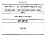
- FIG. 1is a schematic view of a solar cell showing the relative positioning of the principal layers of the solar cell including a transparent conductive oxide film formed in accordance with the present invention
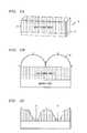
- FIGS. 2A-2Care graphic views showing an embodiment of a planar metal target of indium-zinc used in a reactive sputtering process to form the transparent conductive oxide layer;
- FIGS. 3A-3Care graphic views showing an embodiment of a rotatable metal target of indium-zinc in the form of a rotatable cylinder used in a reactive sputtering process to form the transparent conductive layer;
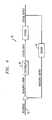
- FIG. 4is a schematic view of a closed-loop feedback control system for controlling the oxygen flow in the reactive sputtering process of the present invention.
- the present inventionis generally directed to a method of forming a transparent conductive oxide film (TCO) on a substrate which can be used as a front contact in the formation of articles such as solar cells and flat display panels.
- a typical solar cell known in the artis identified by reference number 1 .
- the solar cellhas a substrate 2 made of a supporting material such as glass covered by a back contact 3 composed of, for example, molybdenum.
- An absorber layer 4 in the form of a thin filmis spaced between the back contact and a front contact 5 comprised of the transparent conductive oxide.
- the prior art TCO'shave been made from indium-tin oxides or aluminum-doped zinc oxides sputtered from ceramic targets.
- the absorber layer 4is typically a layer comprised of copper-indium selenide (CIS), copper-gallium selenide (CGS), copper-indium-gallium-selenide (CIGS and CIGSS).
- a buffer layer 6typically made of gallium and/or indium oxide is positioned above the absorber layer 4 .
- a transparent resistive oxide (TRO) layer 7is provided between the front contact 5 and the buffer 6 .
- the TROalso referred to as an intrinsic layer, is often made from zinc oxide obtained from sputtering of a ceramic target comprised of zinc oxides or reactive sputtering from a metal zinc target.
- the TROis a low carrier density material which prevents the flow of electrons between the front contact 5 and the absorber layer 4 .
- a method of forming the transparent conductive oxideby sputtering a metal target, preferably comprised of indium and zinc, in a controlled oxygen atmosphere as hereinafter described, to produce a thin film comprised of indium and zinc oxide having properties particularly suited for use as a front contact of a solar cell.
- the TCO films of the present inventionare thinner while exhibiting greater light transmission and lower sheet resistance (ohm/square).
- the TCO of the present inventionis thinner, typically only about half as thick as needed for aluminum-zinc oxide films and exhibits light transmission gains of 3-4%.
- the method of the present inventionis carried out by sputtering an indium-zinc target with a gas mixture that consists of inert gas and reactive gas (e.g. oxygen).
- a gas mixturethat consists of inert gas and reactive gas (e.g. oxygen).
- reactive gase.g. oxygen
- Inert gasessuch as argon are preferred gases for sputtering the metal target.
- the shape of the metal targetcan affect the cost of producing the TCO.
- the targetis a planar target in the shape of a rectangular solid.
- a more preferred metal targetis in the form of a rotatable cylinder.
- a planar target 10 made of indium-zinc (In—Zn)is comprised of an In—Zn layer 11 situated on a backing plate 12 .
- the layer 11is bombarded with an inert gas in an oxygen controlled environment to deposit indium-zinc oxide as the TCO thin film.
- the indium zinc layer 11is comprised of In x Zn 1-x wherein x is from about 0.01 to 0.95, preferably from about 0.6 to 0.9.
- a magnetic field 14(shown in FIG. 2B ) is established proximate the planar target.
- the intensity of the magnetic field over the length of the targeti.e. magnetic field distribution
- the intensity of the magnetic field over the length of the targetis greatest at locations (a) and (b), respectively and decreases toward the center (c) and endpoints (d) and (e).
- the pattern of release of indium and zinc from the targetis greatest at locations (a) and (b) where the intensity of the magnetic field is the greatest.
- the useful life of the planar targetis limited to the extent that the quantity of indium-zinc is exhausted at locations (a) and (b). Conversely, the metal remaining at locations (d), (c), and (e) is unused, which makes the planar target use somewhat inefficient.
- the pattern of usage of the target metal for reactive sputtering in the presence of oxygenis non-uniform and correlates to the magnetic field distribution.
- Target utilizationmay typically be in the range of 25-30%.
- FIGS. 3A-3CA more uniform magnetic field distribution is shown in the embodiment of FIGS. 3A-3C .
- the metal targetis in the form of a rotatable cylinder which during the sputtering process provides a relatively uniform magnetic field distribution.
- FIG. 3Athere is shown an indium-zinc target in the form of a rotatable cylinder (i.e. a rotary target).
- the rotary target 20has a hollow core 22 and a shell 24 comprised of the target metal (e.g. indium-zinc) which is secured to a support or backing tube 26 .
- the targetis rotated during the sputtering process to generate a relatively uniform magnetic field 28 as shown in FIG. 3B .
- the magnetic field distributionis slightly higher than average at the respective ends (f) and (g) of the target, but is relatively continuous over much of the length (h) of the target. Because the magnetic field is relatively uniform over much of the length of the target, utilization of the target material is more uniform, often achieving 70-80% utilization.
- FIG. 3Cthere is shown a representation of a pattern of target erosion typically obtained for a rotary target. Much of the target metal has been released for forming the transparent conductive oxide. Only a relatively small amount of the target material 30 remains on the backing tube 26 . Utilization of the target material is terminated at locations (f) and (g) because the slightly higher than average magnetic field distribution at the respective ends (f) and (g) of the rotary target (see FIG. 3B ) fully erodes the target metal at these locations.
- the indium-zinc metal target in either the planar or rotary formcan be sputtered under moderate pressure of about 3 to 10 mTorr, preferably about 7 m Torr at a moderate power level of about 3 to 15 kW, preferably at about 10 kW.
- the TCO film produced in this mannerprovides a film with a sheet resistance of from about 10 to 90 ohm/square, preferably about 20 ohm/square and a light transmission rate of at least 85% at a thickness of only about 200 to 250 nm, which is up to half the thickness of a transparent conductive film made of aluminum doped zinc oxide from a ceramic target.
- the benefits of using metal targets to produce the transparent conductive oxideare realized in part by controlling the oxygen atmosphere during the sputtering process. If the oxygen content exceeds a desirable level, then the TCO film will be less conductive because of low carrier concentration due to lack of oxygen vacancies. If the oxygen content falls below a desirable level, then the TCO film will exhibit light transmission and be more metal-like due to loss of mobility.
- a feedback control systemis used to monitor and control oxygen levels by associating the oxygen level with a monitorable variable of the system.
- monitorable variablesinclude voltage, O 2 partial pressure and plasma emission.
- FIG. 4there is shown a schematic view of a feedback control system in which a select variable as mentioned above is associated with oxygen levels. The variable is monitored and compared to a standard which correlates with adjustments that may be necessary to the oxygen levels.
- the feedback control system of FIG. 4will be explained below in which voltage is employed as the select variable.
- the feedback control system 30is comprised of a reference 32 which stores a target voltage set point.
- the target voltageis a voltage level that correlates with a desirable oxygen level.
- the desirable oxygen levelis that flow of oxygen into the system which produces a desirable transparent conductive oxide by the reaction of oxygen with metal from the metal target (e.g. InZn).
- a sensor 34continuously measures the actual voltage in the system and generates a signal (measured output) corresponding to the measured voltage which is sent continuously or intermittently to the reference 32 .
- a signalis sent to a controller 36 which monitors the mass flow of oxygen to the system.
- the controlleradjusts the flow of oxygen (system input) until the actual voltage and target voltage are sufficiently similar so that the deviation between the target and actual voltage is either eliminated or sufficiently small that the flow of oxygen to the system is acceptable. For example, if the actual voltage exceeds the target voltage by an amount sufficient to cause a positive deviation (i.e. +deviation), oxygen flow will be increased. Conversely, if the actual voltage is less than the target voltage by an amount sufficient to cause a negative deviation (i.e. ⁇ deviation), oxygen flow will be decreased.
- the feedback control system described in connection with FIG. 4can be modified to employ O 2 partial pressure as the monitorable variable.
- the referenceis configured to establish an O 2 partial pressure set point.
- the sensordetects the actual O 2 pressure while the controller adjusts the oxygen flow to compensate for changes in the O 2 partial pressure.
- the system outputmonitors the actual O 2 partial pressure as detected by the sensor.
- the system inputcorresponds to a signal corresponding to the flow of oxygen from the controller to provide a desirable flow of oxygen to the reactive sputtering process.
- the feedback control systememploys O 2 plasma emission as the monitorable variable.
- the referenceis configured to establish an O 2 plasma emission set point.
- the sensordetects the actual O 2 plasma emission while the controller adjusts the oxygen flow to compensate for changes in the O 2 plasma emission.
- the system outputmonitors the actual O 2 plasma emission as detected by the sensor.
- the system inputcorresponds to the flow of oxygen from the controller to provide a desirable amount of oxygen for the reactive sputtering process.
- the present inventionmay also provide for a transparent resistive oxide (TRO) layer to protect the photovoltaic device from an undesirable flow of electrons.
- TROtransparent resistive oxide
- solar panels employing a TCO in accordance with the present inventionmay also include a transparent resistive oxide layer between the TCO and the buffer. It is preferred in the present invention to employ a TRO comprised of indium-gallium-zinc oxide (IGZO) and/or indium-aluminum-zinc oxide (IAZO).
- IGZOindium-gallium-zinc oxide
- IAZOindium-aluminum-zinc oxide
- the TROcan be produced using metal targets having a desired metal composition (e.g. indium, gallium and zinc) in a manner similar to the method for producing the TCO.
- a metal targetcomprised of indium, gallium and zinc is sputtered in a controlled oxygen atmosphere.
- the targetmay be planar or preferable a rotary target and the system may control the oxygen levels by employing a feedback control system as described in connection with FIG. 4 .
- An InZn targetwas sputtered by argon for twenty-four hours in a continuous operation at a constant power mode at a pressure of about 7 mTorr to produce a TCO on a glass substrate.
- the resulting indium-zinc oxide (IZO) filmhad a thickness of from 243-244 nm, a sheet resistance of from 21.4-21.6 ohm/square and a light transmission rate of from 87%-88%.
- the processwas conducted with the benefit of a closed-loop feedback control of the cathode voltage as described in connection with FIG. 4 .
- a conventional TCO film utilizing a metal target made of AZO (Al:ZnO) with similar electrical properties as the IZO filmhad a thickness of 500-550 nm thickness, a sheet resistance of 23-24 ohm/square and a light transmission rate of 84-85%. Therefore, to achieve similar sheet resistance, only about half of the required AZO film thickness is needed with IZO films prepared in accordance with the present invention with an absolute light transmission gain of 3-4%.
- the deposition rate from an InZn targetwas computed based on typical production runs of solar panels. At a power level of 10 kW, films having a thickness of about 243 nm were produced at a line speed of 40 cm/min.
- the dynamic deposition rate (DDR)was calculated to be 960 nm.cm/min/kW. Converted to effective deposition rate in nm/min, the deposition rate in this example is 756 nm/min at 10 kW. This deposition rate can be increased relatively easily to over 1 ⁇ m/min provided a higher power is used during the sputtering process.
Landscapes
- Chemical & Material Sciences (AREA)
- Engineering & Computer Science (AREA)
- Chemical Kinetics & Catalysis (AREA)
- Materials Engineering (AREA)
- Mechanical Engineering (AREA)
- Metallurgy (AREA)
- Organic Chemistry (AREA)
- Physics & Mathematics (AREA)
- Fluid Mechanics (AREA)
- Condensed Matter Physics & Semiconductors (AREA)
- Manufacturing & Machinery (AREA)
- Computer Hardware Design (AREA)
- Microelectronics & Electronic Packaging (AREA)
- Power Engineering (AREA)
- General Physics & Mathematics (AREA)
- Physical Vapour Deposition (AREA)
- Manufacturing Of Electric Cables (AREA)
Abstract
Description
- This application claims priority of U.S. Provisional Patent Application No. 61/206,877 filed Feb. 4, 2009.
- The present invention relates generally to the field of forming transparent conductive oxide films and particularly to the formation of transparent conductive oxide films by reactive sputtering of a metal target containing indium.
- Transparent conductive oxides (TCO) in the form of thin films are useful as an electrical contact in a variety of applications including photovoltaics (e.g. the fabrication of solar electric panels) and in flat-panel displays.
- It is known in the art to form TCOs by sputtering aluminum-doped zinc oxide or indium zinc oxides from a ceramic (non-metal) target. Ceramic targets are desirable because they achieve relatively high performance and are generally reliable. Despite these advantages, ceramic targets suffer from a number of disadvantages. The deposition rates of the TCO from a ceramic target are lower than desired, which adds to the time and cost of depositing the TCO and forming solar panels. In addition, the thickness of the TCO formed from conventional aluminum-doped zinc oxide ceramic targets exceeds what is necessary to obtain a desired conductivity. Still further sputtering of aluminum-doped zinc oxide ceramic targets requires relatively high temperatures adding to the cost of the process.
- It is therefore desirable to provide a method of producing transparent conductive oxide films in a manner which is cost effective and yet achieves desired high performance and high reliability.
- The present invention is generally directed to a method of forming a transparent conductive oxide film useful for the production of solar cells, flat panel displays and the like. The method employs reactive sputtering from a metal target. Reactive sputtering requires bombarding a metal target in an oxygen containing atmosphere so that the metal atoms react with oxygen to form the corresponding oxide which is deposited on a suitable substrate. In the present invention, the metal target at least includes indium. Thus, the reactive sputtering process of the present invention leads to the formation of an indium-containing transparent conductive oxide. The present method is a departure from conventional methods which utilize ceramic targets containing oxides such as aluminum-doped zinc oxides and indium zinc oxides.
- In one embodiment of the present invention, there is provided:
- A method of forming an indium-containing transparent conductive oxide film comprising:
- a) reactive sputtering from a metal target comprising indium in an oxygen-containing atmosphere to form an indium-containing oxide; and
- b) depositing the indium-containing oxide on a substrate to form said transparent conductive oxide film.
- In a further embodiment of the invention, the method is conducted with a rotatable cylindrical target which provides a more uniform magnetic field distribution and thus obtains more efficient use of the target material.
- In a further embodiment of the invention, there is provided a metal target comprising indium and zinc which can be sputtered in the presence of oxygen to form an indium-zinc transparent conductive oxide.
- In a still further embodiment of the invention, there is provided a photovoltaic device, as for example a solar cell, employing an indium-containing transparent conductive oxide film formed by the method described above.
- The following drawings in which like reference characters indicate like parts are illustrative of embodiments of the invention and are not intended to limit the invention as encompassed by the claims forming part of the application.
FIG. 1 is a schematic view of a solar cell showing the relative positioning of the principal layers of the solar cell including a transparent conductive oxide film formed in accordance with the present invention;FIGS. 2A-2C are graphic views showing an embodiment of a planar metal target of indium-zinc used in a reactive sputtering process to form the transparent conductive oxide layer;FIGS. 3A-3C are graphic views showing an embodiment of a rotatable metal target of indium-zinc in the form of a rotatable cylinder used in a reactive sputtering process to form the transparent conductive layer; andFIG. 4 is a schematic view of a closed-loop feedback control system for controlling the oxygen flow in the reactive sputtering process of the present invention.- The present invention is generally directed to a method of forming a transparent conductive oxide film (TCO) on a substrate which can be used as a front contact in the formation of articles such as solar cells and flat display panels. As shown in
FIG. 1 , a typical solar cell known in the art is identified by reference number1. The solar cell has a substrate2 made of a supporting material such as glass covered by a back contact3 composed of, for example, molybdenum. An absorber layer4 in the form of a thin film is spaced between the back contact and a front contact5 comprised of the transparent conductive oxide. The prior art TCO's have been made from indium-tin oxides or aluminum-doped zinc oxides sputtered from ceramic targets. The absorber layer4 is typically a layer comprised of copper-indium selenide (CIS), copper-gallium selenide (CGS), copper-indium-gallium-selenide (CIGS and CIGSS). - A buffer layer6, typically made of gallium and/or indium oxide is positioned above the absorber layer4. Optionally a transparent resistive oxide (TRO) layer7 is provided between the front contact5 and the buffer6. The TRO, also referred to as an intrinsic layer, is often made from zinc oxide obtained from sputtering of a ceramic target comprised of zinc oxides or reactive sputtering from a metal zinc target. The TRO is a low carrier density material which prevents the flow of electrons between the front contact5 and the absorber layer4.
- In accordance with the present invention, there is provided a method of forming the transparent conductive oxide by sputtering a metal target, preferably comprised of indium and zinc, in a controlled oxygen atmosphere as hereinafter described, to produce a thin film comprised of indium and zinc oxide having properties particularly suited for use as a front contact of a solar cell.
- As compared with conventional TCO films made of aluminum-zinc oxide, the TCO films of the present invention are thinner while exhibiting greater light transmission and lower sheet resistance (ohm/square). In particular, to achieve similar sheet resistance, the TCO of the present invention is thinner, typically only about half as thick as needed for aluminum-zinc oxide films and exhibits light transmission gains of 3-4%.
- The method of the present invention is carried out by sputtering an indium-zinc target with a gas mixture that consists of inert gas and reactive gas (e.g. oxygen). The principles of reactive sputtering are described in Reactive Sputter Deposition, Springer Series in Materials Science, Volume 109. Eds. Diederik Depla and Stijn Mahieu (2008). Inert gases such as argon are preferred gases for sputtering the metal target. The shape of the metal target can affect the cost of producing the TCO. In one embodiment of the invention, the target is a planar target in the shape of a rectangular solid. A more preferred metal target is in the form of a rotatable cylinder.
- As shown in
FIG. 2A , aplanar target 10 made of indium-zinc (In—Zn) is comprised of an In—Zn layer 11 situated on abacking plate 12. Thelayer 11 is bombarded with an inert gas in an oxygen controlled environment to deposit indium-zinc oxide as the TCO thin film. Theindium zinc layer 11 is comprised of InxZn1-xwherein x is from about 0.01 to 0.95, preferably from about 0.6 to 0.9. - During the sputtering process, a magnetic field14 (shown in
FIG. 2B ) is established proximate the planar target. The intensity of the magnetic field over the length of the target (i.e. magnetic field distribution) is greatest at locations (a) and (b), respectively and decreases toward the center (c) and endpoints (d) and (e). Accordingly, the pattern of release of indium and zinc from the target is greatest at locations (a) and (b) where the intensity of the magnetic field is the greatest. As can be observed fromFIG. 2C , the useful life of the planar target is limited to the extent that the quantity of indium-zinc is exhausted at locations (a) and (b). Conversely, the metal remaining at locations (d), (c), and (e) is unused, which makes the planar target use somewhat inefficient. - As shown in
FIGS. 2A-2C , the pattern of usage of the target metal for reactive sputtering in the presence of oxygen is non-uniform and correlates to the magnetic field distribution. Target utilization may typically be in the range of 25-30%. - A more uniform magnetic field distribution is shown in the embodiment of
FIGS. 3A-3C . - In accordance with a preferred embodiment of the invention, the metal target is in the form of a rotatable cylinder which during the sputtering process provides a relatively uniform magnetic field distribution. Referring to
FIG. 3A , there is shown an indium-zinc target in the form of a rotatable cylinder (i.e. a rotary target). Therotary target 20 has ahollow core 22 and ashell 24 comprised of the target metal (e.g. indium-zinc) which is secured to a support or backingtube 26. The target is rotated during the sputtering process to generate a relatively uniformmagnetic field 28 as shown inFIG. 3B . The magnetic field distribution is slightly higher than average at the respective ends (f) and (g) of the target, but is relatively continuous over much of the length (h) of the target. Because the magnetic field is relatively uniform over much of the length of the target, utilization of the target material is more uniform, often achieving 70-80% utilization. - Referring to
FIG. 3C , there is shown a representation of a pattern of target erosion typically obtained for a rotary target. Much of the target metal has been released for forming the transparent conductive oxide. Only a relatively small amount of thetarget material 30 remains on thebacking tube 26. Utilization of the target material is terminated at locations (f) and (g) because the slightly higher than average magnetic field distribution at the respective ends (f) and (g) of the rotary target (seeFIG. 3B ) fully erodes the target metal at these locations. - The indium-zinc metal target in either the planar or rotary form can be sputtered under moderate pressure of about 3 to 10 mTorr, preferably about 7 m Torr at a moderate power level of about 3 to 15 kW, preferably at about 10 kW. The TCO film produced in this manner provides a film with a sheet resistance of from about 10 to 90 ohm/square, preferably about 20 ohm/square and a light transmission rate of at least 85% at a thickness of only about 200 to 250 nm, which is up to half the thickness of a transparent conductive film made of aluminum doped zinc oxide from a ceramic target.
- The benefits of using metal targets to produce the transparent conductive oxide are realized in part by controlling the oxygen atmosphere during the sputtering process. If the oxygen content exceeds a desirable level, then the TCO film will be less conductive because of low carrier concentration due to lack of oxygen vacancies. If the oxygen content falls below a desirable level, then the TCO film will exhibit light transmission and be more metal-like due to loss of mobility.
- Accordingly, in a further embodiment of the invention, means are provided to control the oxygen atmosphere during the sputtering process. In a preferred embodiment, a feedback control system is used to monitor and control oxygen levels by associating the oxygen level with a monitorable variable of the system. Such monitorable variables include voltage, O2partial pressure and plasma emission.
- Referring to
FIG. 4 , there is shown a schematic view of a feedback control system in which a select variable as mentioned above is associated with oxygen levels. The variable is monitored and compared to a standard which correlates with adjustments that may be necessary to the oxygen levels. The feedback control system ofFIG. 4 will be explained below in which voltage is employed as the select variable. - The
feedback control system 30 is comprised of areference 32 which stores a target voltage set point. The target voltage is a voltage level that correlates with a desirable oxygen level. The desirable oxygen level is that flow of oxygen into the system which produces a desirable transparent conductive oxide by the reaction of oxygen with metal from the metal target (e.g. InZn). - A
sensor 34 continuously measures the actual voltage in the system and generates a signal (measured output) corresponding to the measured voltage which is sent continuously or intermittently to thereference 32. When a deviation between the target voltage and the actual voltage is detected, a signal is sent to acontroller 36 which monitors the mass flow of oxygen to the system. The controller adjusts the flow of oxygen (system input) until the actual voltage and target voltage are sufficiently similar so that the deviation between the target and actual voltage is either eliminated or sufficiently small that the flow of oxygen to the system is acceptable. For example, if the actual voltage exceeds the target voltage by an amount sufficient to cause a positive deviation (i.e. +deviation), oxygen flow will be increased. Conversely, if the actual voltage is less than the target voltage by an amount sufficient to cause a negative deviation (i.e. −deviation), oxygen flow will be decreased. - The feedback control system described in connection with
FIG. 4 can be modified to employ O2partial pressure as the monitorable variable. In this embodiment, the reference is configured to establish an O2partial pressure set point. The sensor detects the actual O2pressure while the controller adjusts the oxygen flow to compensate for changes in the O2partial pressure. The system output monitors the actual O2partial pressure as detected by the sensor. The system input corresponds to a signal corresponding to the flow of oxygen from the controller to provide a desirable flow of oxygen to the reactive sputtering process. - Another use of the feedback control system employs O2plasma emission as the monitorable variable. In this embodiment, the reference is configured to establish an O2plasma emission set point. The sensor detects the actual O2plasma emission while the controller adjusts the oxygen flow to compensate for changes in the O2plasma emission. The system output monitors the actual O2plasma emission as detected by the sensor. The system input corresponds to the flow of oxygen from the controller to provide a desirable amount of oxygen for the reactive sputtering process.
- The present invention may also provide for a transparent resistive oxide (TRO) layer to protect the photovoltaic device from an undesirable flow of electrons.
- As indicated in connection with
FIG. 1 , solar panels employing a TCO in accordance with the present invention may also include a transparent resistive oxide layer between the TCO and the buffer. It is preferred in the present invention to employ a TRO comprised of indium-gallium-zinc oxide (IGZO) and/or indium-aluminum-zinc oxide (IAZO). - The TRO can be produced using metal targets having a desired metal composition (e.g. indium, gallium and zinc) in a manner similar to the method for producing the TCO. For example, a metal target comprised of indium, gallium and zinc is sputtered in a controlled oxygen atmosphere. The target may be planar or preferable a rotary target and the system may control the oxygen levels by employing a feedback control system as described in connection with
FIG. 4 . - An InZn target was sputtered by argon for twenty-four hours in a continuous operation at a constant power mode at a pressure of about 7 mTorr to produce a TCO on a glass substrate. The resulting indium-zinc oxide (IZO) film had a thickness of from 243-244 nm, a sheet resistance of from 21.4-21.6 ohm/square and a light transmission rate of from 87%-88%. The process was conducted with the benefit of a closed-loop feedback control of the cathode voltage as described in connection with
FIG. 4 . - As a comparison, a conventional TCO film utilizing a metal target made of AZO (Al:ZnO) with similar electrical properties as the IZO film had a thickness of 500-550 nm thickness, a sheet resistance of 23-24 ohm/square and a light transmission rate of 84-85%. Therefore, to achieve similar sheet resistance, only about half of the required AZO film thickness is needed with IZO films prepared in accordance with the present invention with an absolute light transmission gain of 3-4%.
- The deposition rate from an InZn target was computed based on typical production runs of solar panels. At a power level of 10 kW, films having a thickness of about 243 nm were produced at a line speed of 40 cm/min. The dynamic deposition rate (DDR) was calculated to be 960 nm.cm/min/kW. Converted to effective deposition rate in nm/min, the deposition rate in this example is 756 nm/min at 10 kW. This deposition rate can be increased relatively easily to over 1 μm/min provided a higher power is used during the sputtering process.
Claims (26)
1. A method of forming an indium-containing transparent conductive oxide film comprising:
a) reactive sputtering a metal target comprising indium in an oxygen-containing atmosphere to form an indium-containing oxide
b) depositing the indium oxide on a substrate to form said transparent conductive oxide film.
2. The method ofclaim 1 wherein the metal target further comprises a metal selected from the group consisting of zinc, gallium and aluminum and combinations thereof.
3. The method ofclaim 1 wherein the step of reactive sputtering comprises contacting the metal target with an inert gas under conditions sufficient to sputter the metal from the target.
4. The method ofclaim 3 wherein the inert gas is argon.
5. The method ofclaim 1 further comprising controlling the quantity of oxygen in the oxygen-containing atmosphere.
6. The method ofclaim 5 wherein the step of controlling the quantity of oxygen comprises monitoring a variable selected from the group consisting of voltage, O2partial pressure and O2plasma emission and associating the variable with the flow of oxygen.
7. The method ofclaim 1 wherein the metallic target is in the form of a rotatable cylinder.
8. The method ofclaim 1 wherein the metallic target is planar.
9. The method ofclaim 1 wherein the metal target comprises indium and zinc.
10. The method ofclaim 9 wherein the step of the reactive sputtering frees indium and zinc from the target.
11. The method ofclaim 9 wherein the target comprises InxZn1-xwherein x is in the range of from about 0.01 to 0.95.
12. The method ofclaim 11 wherein x is in the range of from about 0.6 to 0.9.
13. A photovoltaic device comprising a substrate, a transparent conductive layer and an absorber layer between the substrate and the transparent conductive layer, said transparent conductive layer formed by the method ofclaim 1 .
14. The photovoltaic device ofclaim 13 wherein the metal target further comprises a metal selected from the group consisting of zinc, gallium and aluminum and combinations thereof.
15. The photovoltaic device ofclaim 13 wherein the step of reactive sputtering comprises contacting the metal target with an inert gas under conditions sufficient to free the metal atoms from the target surface.
16. The photovoltaic device ofclaim 15 wherein the inert gas is argon.
17. The photovoltaic device ofclaim 13 further comprising controlling the quantity of oxygen in the oxygen containing atmosphere.
18. The photovoltaic device ofclaim 17 wherein the step of controlling the quantity of oxygen comprises monitoring a variable from the group consisting of voltage, O2partial pressure and O2plasma emission and associating the variable with the flow of oxygen.
19. The photovoltaic device ofclaim 13 wherein the metallic target is in the form of a rotatable cylinder.
20. The photovoltaic device ofclaim 13 wherein the metallic target is planar.
21. The photovoltaic device ofclaim 13 wherein the metal target comprises indium and zinc.
22. The photovoltaic device ofclaim 13 wherein the target comprises InxZn1-xand wherein x is in the range of from about 0.01 to 0.95.
23. The photovoltaic device ofclaim 22 wherein x is in the range of from about 0.6 to 0.9.
24. The photovoltaic device ofclaim 13 further comprising a transparent resistive layer between the transparent conductive layer and absorber layer.
25. The photovoltaic device ofclaim 24 wherein the transparent resistive layer comprises an oxide selected from IGZO and IAZO.
26. The photovoltaic device ofclaim 13 having a light transmission rate of at least 85%.
Priority Applications (1)
| Application Number | Priority Date | Filing Date | Title |
|---|---|---|---|
| US12/658,203US20100258180A1 (en) | 2009-02-04 | 2010-02-04 | Method of forming an indium-containing transparent conductive oxide film, metal targets used in the method and photovoltaic devices utilizing said films |
Applications Claiming Priority (2)
| Application Number | Priority Date | Filing Date | Title |
|---|---|---|---|
| US20687709P | 2009-02-04 | 2009-02-04 | |
| US12/658,203US20100258180A1 (en) | 2009-02-04 | 2010-02-04 | Method of forming an indium-containing transparent conductive oxide film, metal targets used in the method and photovoltaic devices utilizing said films |
Publications (1)
| Publication Number | Publication Date |
|---|---|
| US20100258180A1true US20100258180A1 (en) | 2010-10-14 |
Family
ID=42542337
Family Applications (1)
| Application Number | Title | Priority Date | Filing Date |
|---|---|---|---|
| US12/658,203AbandonedUS20100258180A1 (en) | 2009-02-04 | 2010-02-04 | Method of forming an indium-containing transparent conductive oxide film, metal targets used in the method and photovoltaic devices utilizing said films |
Country Status (6)
| Country | Link |
|---|---|
| US (1) | US20100258180A1 (en) |
| EP (1) | EP2393955A4 (en) |
| KR (1) | KR20110111369A (en) |
| AU (1) | AU2010211053A1 (en) |
| CA (1) | CA2740363A1 (en) |
| WO (1) | WO2010090740A1 (en) |
Cited By (1)
| Publication number | Priority date | Publication date | Assignee | Title |
|---|---|---|---|---|
| US20110226337A1 (en)* | 2010-03-17 | 2011-09-22 | Hiroshi Deguchi | Thin-film solar battery and method for producing the same |
Families Citing this family (1)
| Publication number | Priority date | Publication date | Assignee | Title |
|---|---|---|---|---|
| KR20130087354A (en)* | 2012-01-27 | 2013-08-06 | 주식회사 유피케미칼 | Indium-containing oxide film and producing method thereof |
Citations (93)
| Publication number | Priority date | Publication date | Assignee | Title |
|---|---|---|---|---|
| US4088544A (en)* | 1976-04-19 | 1978-05-09 | Hutkin Irving J | Composite and method for making thin copper foil |
| US4267398A (en)* | 1979-05-29 | 1981-05-12 | University Of Delaware | Thin film photovoltaic cells |
| US4315097A (en)* | 1980-10-27 | 1982-02-09 | Mcdonnell Douglas Corporation | Back contacted MIS photovoltaic cell |
| US4322571A (en)* | 1980-07-17 | 1982-03-30 | The Boeing Company | Solar cells and methods for manufacture thereof |
| US4392451A (en)* | 1980-12-31 | 1983-07-12 | The Boeing Company | Apparatus for forming thin-film heterojunction solar cells employing materials selected from the class of I-III-VI2 chalcopyrite compounds |
| US4479847A (en)* | 1981-12-30 | 1984-10-30 | California Institute Of Technology | Equilibrium crystal growth from substrate confined liquid |
| US4523051A (en)* | 1983-09-27 | 1985-06-11 | The Boeing Company | Thin films of mixed metal compounds |
| USRE31968E (en)* | 1980-12-31 | 1985-08-13 | The Boeing Company | Methods for forming thin-film heterojunction solar cells from I-III-VI.sub.2 |
| US4571448A (en)* | 1981-11-16 | 1986-02-18 | University Of Delaware | Thin film photovoltaic solar cell and method of making the same |
| US4609820A (en)* | 1983-04-07 | 1986-09-02 | Fujitsu Limited | Optical shield for image sensing device |
| US4611091A (en)* | 1984-12-06 | 1986-09-09 | Atlantic Richfield Company | CuInSe2 thin film solar cell with thin CdS and transparent window layer |
| US4674434A (en)* | 1984-07-09 | 1987-06-23 | Canon Kabushiki Kaisha | Apparatus for forming deposited film |
| US4823176A (en)* | 1987-04-03 | 1989-04-18 | General Electric Company | Vertical double diffused metal oxide semiconductor (VDMOS) device including high voltage junction exhibiting increased safe operating area |
| US4864599A (en)* | 1987-07-31 | 1989-09-05 | Nec Corporation | Registration of a new cordless telephone to an existing system |
| US4902398A (en)* | 1988-04-27 | 1990-02-20 | American Thim Film Laboratories, Inc. | Computer program for vacuum coating systems |
| US4902668A (en)* | 1988-08-25 | 1990-02-20 | Minnesota Mining And Manufacturing Company | Pressure sensitive carbonless imaging system incorporating uncolored ferric organophosphates and colored chelates |
| US4902395A (en)* | 1986-11-25 | 1990-02-20 | Mitsubishi Kinzoku Kabushiki | Method of manufacturing surface coated carbo-nitride titanium-base cermet materials for inserts of high-speed cutting tools |
| US5028274A (en)* | 1989-06-07 | 1991-07-02 | International Solar Electric Technology, Inc. | Group I-III-VI2 semiconductor films for solar cell application |
| US5055150A (en)* | 1989-02-03 | 1991-10-08 | Alcan International Limited | Process and apparatus for producing coated polymer sheets having oxygen and moisture barrier properties and coated polymer sheets thus produced |
| US5124308A (en)* | 1989-11-17 | 1992-06-23 | Albin Loren D | Monosubstituted dithiooxamide compounds and their use |
| US5124309A (en)* | 1989-03-28 | 1992-06-23 | Dai Nippon Insatsu Kabushiki Kaisha | Heat transfer sheet |
| US5178967A (en)* | 1989-02-03 | 1993-01-12 | Alcan International Limited | Bilayer oxide film and process for producing same |
| US5248621A (en)* | 1990-10-23 | 1993-09-28 | Canon Kabushiki Kaisha | Method for producing solar cell devices of crystalline material |
| US5298449A (en)* | 1992-03-06 | 1994-03-29 | Nec Corporation | Semiconductor substrate having a silicon-on-insulator structure and method of fabricating the same |
| US5396839A (en)* | 1992-09-23 | 1995-03-14 | Col1Or | Apparatus and method for printing color images |
| US5405802A (en)* | 1992-01-31 | 1995-04-11 | Canon Kabushiki Kaisha | Process of fabricating a semiconductor substrate |
| US5436204A (en)* | 1993-04-12 | 1995-07-25 | Midwest Research Institute | Recrystallization method to selenization of thin-film Cu(In,Ga)Se2 for semiconductor device applications |
| JPH07207440A (en)* | 1994-01-18 | 1995-08-08 | Asahi Glass Co Ltd | Reactive sputter film forming method and film forming apparatus |
| US5441897A (en)* | 1993-04-12 | 1995-08-15 | Midwest Research Institute | Method of fabricating high-efficiency Cu(In,Ga)(SeS)2 thin films for solar cells |
| US5567469A (en)* | 1992-10-30 | 1996-10-22 | Matsuhita Electric Co., Ltd. | Process for producing chalcopyrite type compound thin film |
| US5578503A (en)* | 1992-09-22 | 1996-11-26 | Siemens Aktiengesellschaft | Rapid process for producing a chalcopyrite semiconductor on a substrate |
| US5626688A (en)* | 1994-12-01 | 1997-05-06 | Siemens Aktiengesellschaft | Solar cell with chalcopyrite absorber layer |
| US5674555A (en)* | 1995-11-30 | 1997-10-07 | University Of Delaware | Process for preparing group Ib-IIIa-VIa semiconducting films |
| US5687218A (en)* | 1990-02-15 | 1997-11-11 | Canon Kabushiki Kaisha | Cordless telephone |
| US5705011A (en)* | 1993-01-08 | 1998-01-06 | Poly-Bond, Inc. | Method of making composite with discontinuous adhesive structure |
| US5730852A (en)* | 1995-09-25 | 1998-03-24 | Davis, Joseph & Negley | Preparation of cuxinygazsen (X=0-2, Y=0-2, Z=0-2, N=0-3) precursor films by electrodeposition for fabricating high efficiency solar cells |
| US5756240A (en)* | 1997-01-24 | 1998-05-26 | Eastman Kodak Company | Method of making color filter arrays by transferring colorant material |
| US5759954A (en)* | 1994-10-20 | 1998-06-02 | Matsushita Electric Industrial Co., Ltd. | Transfer member and thermal transfer printing method |
| US5794163A (en)* | 1993-07-27 | 1998-08-11 | Spectralink Corporation | Headset for hands-free wireless telephone |
| US5858628A (en)* | 1996-09-13 | 1999-01-12 | Dai Nippon Printing Co., Ltd. | Black thermal transfer sheet |
| US5858121A (en)* | 1995-09-13 | 1999-01-12 | Matsushita Electric Industrial Co., Ltd. | Thin film solar cell and method for manufacturing the same |
| US5942089A (en)* | 1996-04-22 | 1999-08-24 | Northwestern University | Method for sputtering compounds on a substrate |
| US5948176A (en)* | 1997-09-29 | 1999-09-07 | Midwest Research Institute | Cadmium-free junction fabrication process for CuInSe2 thin film solar cells |
| US5972527A (en)* | 1992-12-15 | 1999-10-26 | Idemitsu Kosan Co., Ltd. | Transparent electrically conductive layer, electrically conductive transparent substrate and electrically conductive material |
| US6021207A (en)* | 1997-04-03 | 2000-02-01 | Resound Corporation | Wireless open ear canal earpiece |
| US6026082A (en)* | 1996-11-27 | 2000-02-15 | Telergy, Inc. | Wireless communication system |
| US6072818A (en)* | 1996-03-28 | 2000-06-06 | Fuji Photo Film Co., Ltd. | Semiconductor light emission device |
| US6100165A (en)* | 1996-11-15 | 2000-08-08 | Canon Kabushiki Kaisha | Method of manufacturing semiconductor article |
| US6121541A (en)* | 1997-07-28 | 2000-09-19 | Bp Solarex | Monolithic multi-junction solar cells with amorphous silicon and CIS and their alloys |
| US6141356A (en)* | 1997-11-10 | 2000-10-31 | Ameritech Corporation | System and method for distributing voice and data information over wireless and wireline networks |
| US6185418B1 (en)* | 1997-11-07 | 2001-02-06 | Lucent Technologies Inc. | Adaptive digital radio communication system |
| US6187653B1 (en)* | 1999-12-17 | 2001-02-13 | Lucent Technologies, Inc. | Method for attractive bonding of two crystalline substrates |
| US6190453B1 (en)* | 1999-07-14 | 2001-02-20 | Seh America, Inc. | Growth of epitaxial semiconductor material with improved crystallographic properties |
| US6225190B1 (en)* | 1996-12-09 | 2001-05-01 | Commissariat A L'energie Atomique | Process for the separation of at least two elements of a structure in contact with one another by ion implantation |
| US6225199B1 (en)* | 1998-07-07 | 2001-05-01 | Samsung Electronics Co., Ltd. | Semiconductor device having triple-well |
| US6251754B1 (en)* | 1997-05-09 | 2001-06-26 | Denso Corporation | Semiconductor substrate manufacturing method |
| US6339695B1 (en)* | 1999-05-05 | 2002-01-15 | Radioshack Corporation | Cordless phone data transfer |
| US20020006470A1 (en)* | 1997-10-02 | 2002-01-17 | Chris Eberspacher | Method for forming particulate materials |
| US20020016188A1 (en)* | 2000-06-22 | 2002-02-07 | Iwao Kashiwamura | Wireless transceiver set |
| US6372538B1 (en)* | 2000-03-16 | 2002-04-16 | University Of Delaware | Fabrication of thin-film, flexible photovoltaic module |
| US20020043279A1 (en)* | 1999-11-25 | 2002-04-18 | Franz Karg | Diode structure, especially for thin-filn solar cells |
| US6455398B1 (en)* | 1999-07-16 | 2002-09-24 | Massachusetts Institute Of Technology | Silicon on III-V semiconductor bonding for monolithic optoelectronic integration |
| US6517687B1 (en)* | 1999-03-17 | 2003-02-11 | General Electric Company | Ultraviolet filters with enhanced weatherability and method of making |
| US6521511B1 (en)* | 1997-07-03 | 2003-02-18 | Seiko Epson Corporation | Thin film device transfer method, thin film device, thin film integrated circuit device, active matrix board, liquid crystal display, and electronic apparatus |
| US20030054662A1 (en)* | 2001-09-20 | 2003-03-20 | Stanbery Billy J. | Synthesis of layers, coatings or films using surfactants |
| US20030051664A1 (en)* | 2001-09-20 | 2003-03-20 | Helio Volt Corp | Apparatus for the synthesis of layers, coatings or films |
| US20030054663A1 (en)* | 2001-09-20 | 2003-03-20 | Stanbery Billy J. | Synthesis of layers, coatings or films using collection layer |
| US20030054582A1 (en)* | 2001-09-20 | 2003-03-20 | Stanbery Billy J. | Synthesis of layers, coatings or films using precursor layer exerted pressure containment |
| US6559372B2 (en)* | 2001-09-20 | 2003-05-06 | Heliovolt Corporation | Photovoltaic devices and compositions for use therein |
| US6593213B2 (en)* | 2001-09-20 | 2003-07-15 | Heliovolt Corporation | Synthesis of layers, coatings or films using electrostatic fields |
| US20030201010A1 (en)* | 1999-06-30 | 2003-10-30 | Catalysts & Chemicals Industries Co., Ltd. | Photovoltaic cell |
| US6852920B2 (en)* | 2002-06-22 | 2005-02-08 | Nanosolar, Inc. | Nano-architected/assembled solar electricity cell |
| US6855202B2 (en)* | 2001-11-30 | 2005-02-15 | The Regents Of The University Of California | Shaped nanocrystal particles and methods for making the same |
| US20050095422A1 (en)* | 2003-10-31 | 2005-05-05 | Nanosolar, Inc. | Inorganic/organic hybrid nanolaminate barrier film |
| US20050098204A1 (en)* | 2003-05-21 | 2005-05-12 | Nanosolar, Inc. | Photovoltaic devices fabricated from nanostructured template |
| US20050098205A1 (en)* | 2003-05-21 | 2005-05-12 | Nanosolar, Inc. | Photovoltaic devices fabricated from insulating nanostructured template |
| US20050121068A1 (en)* | 2002-06-22 | 2005-06-09 | Nanosolar, Inc. | Photovoltaic devices fabricated by growth from porous template |
| US20050183767A1 (en)* | 2004-02-19 | 2005-08-25 | Nanosolar, Inc. | Solution-based fabrication of photovoltaic cell |
| US20050186342A1 (en)* | 2004-02-19 | 2005-08-25 | Nanosolar, Inc. | Formation of CIGS absorber layer materials using atomic layer deposition and high throughput surface treatment |
| US20050183768A1 (en)* | 2004-02-19 | 2005-08-25 | Nanosolar, Inc. | Photovoltaic thin-film cell produced from metallic blend using high-temperature printing |
| US6936761B2 (en)* | 2003-03-29 | 2005-08-30 | Nanosolar, Inc. | Transparent electrode, optoelectronic apparatus and devices |
| US20050218377A1 (en)* | 2004-03-31 | 2005-10-06 | Solaris Nanosciences, Inc. | Anisotropic nanoparticles and anisotropic nanostructures and pixels, displays and inks using them |
| US6987071B1 (en)* | 2003-11-21 | 2006-01-17 | Nanosolar, Inc. | Solvent vapor infiltration of organic materials into nanostructures |
| US7014741B2 (en)* | 2003-02-21 | 2006-03-21 | Von Ardenne Anlagentechnik Gmbh | Cylindrical magnetron with self cleaning target |
| US20060062902A1 (en)* | 2004-09-18 | 2006-03-23 | Nanosolar, Inc. | Coated nanoparticles and quantum dots for solution-based fabrication of photovoltaic cells |
| US7045205B1 (en)* | 2004-02-19 | 2006-05-16 | Nanosolar, Inc. | Device based on coated nanoporous structure |
| US7097902B2 (en)* | 2003-12-22 | 2006-08-29 | Eastman Kodak Company | Self assembled organic nanocrystal superlattices |
| US20070077429A1 (en)* | 2004-02-20 | 2007-04-05 | Mirkin Chad A | Multicomponent nanorods |
| US20070119522A1 (en)* | 2005-07-08 | 2007-05-31 | New York University and the Trustees of Princeton University | Assembly of quasicrystalline photonic heterostructures |
| US20070152236A1 (en)* | 2005-12-29 | 2007-07-05 | Halpert Jonathan E | Semiconductor nanocrystal heterostructures |
| US20070163642A1 (en)* | 2004-02-19 | 2007-07-19 | Nanosolar, Inc. | High-throughput printing of semiconductor precursor layer from inter-metallic microflake articles |
| US20100038240A1 (en)* | 2005-06-22 | 2010-02-18 | W. C. Heraeus Gmbh | Powder-Fiber Adhesive |
| US8153031B2 (en)* | 2007-05-11 | 2012-04-10 | Idemitsu Kosan Co., Ltd. | In-Ga-Zn-Sn type oxide sinter and target for physical film deposition |
Family Cites Families (6)
| Publication number | Priority date | Publication date | Assignee | Title |
|---|---|---|---|---|
| JPH1129863A (en)* | 1997-07-10 | 1999-02-02 | Canon Inc | Deposition film manufacturing method |
| DE60041353D1 (en)* | 1999-11-25 | 2009-02-26 | Idemitsu Kosan Co | SPUTTERTARGET, TRANSPARENT CONDUCTIVE OXID AND PREPARATION PROCESS FOR SPUTTERTARGET |
| EP1451009A1 (en)* | 2001-09-14 | 2004-09-01 | CPFilms Inc. | Durable, low ohm, high transmission transparent conductor |
| WO2006041199A1 (en)* | 2004-10-13 | 2006-04-20 | Teijin Dupont Films Japan Limited | Multilayer body for dye-sensitized solar cell, electrode for dye-sensitized solar cell and method for producing same |
| KR101150142B1 (en)* | 2006-04-06 | 2012-06-11 | 어플라이드 머티어리얼스, 인코포레이티드 | Reactive sputtering zinc oxide transparent conductive oxides onto large area substrates |
| US7582161B2 (en)* | 2006-04-07 | 2009-09-01 | Micron Technology, Inc. | Atomic layer deposited titanium-doped indium oxide films |
- 2010
- 2010-02-04EPEP10738859.7Apatent/EP2393955A4/ennot_activeWithdrawn
- 2010-02-04WOPCT/US2010/000310patent/WO2010090740A1/enactiveApplication Filing
- 2010-02-04USUS12/658,203patent/US20100258180A1/ennot_activeAbandoned
- 2010-02-04CACA2740363Apatent/CA2740363A1/ennot_activeAbandoned
- 2010-02-04KRKR1020117012059Apatent/KR20110111369A/ennot_activeCeased
- 2010-02-04AUAU2010211053Apatent/AU2010211053A1/ennot_activeAbandoned
Patent Citations (100)
| Publication number | Priority date | Publication date | Assignee | Title |
|---|---|---|---|---|
| US4088544A (en)* | 1976-04-19 | 1978-05-09 | Hutkin Irving J | Composite and method for making thin copper foil |
| US4267398A (en)* | 1979-05-29 | 1981-05-12 | University Of Delaware | Thin film photovoltaic cells |
| US4322571A (en)* | 1980-07-17 | 1982-03-30 | The Boeing Company | Solar cells and methods for manufacture thereof |
| US4315097A (en)* | 1980-10-27 | 1982-02-09 | Mcdonnell Douglas Corporation | Back contacted MIS photovoltaic cell |
| US4392451A (en)* | 1980-12-31 | 1983-07-12 | The Boeing Company | Apparatus for forming thin-film heterojunction solar cells employing materials selected from the class of I-III-VI2 chalcopyrite compounds |
| USRE31968E (en)* | 1980-12-31 | 1985-08-13 | The Boeing Company | Methods for forming thin-film heterojunction solar cells from I-III-VI.sub.2 |
| US4571448A (en)* | 1981-11-16 | 1986-02-18 | University Of Delaware | Thin film photovoltaic solar cell and method of making the same |
| US4479847A (en)* | 1981-12-30 | 1984-10-30 | California Institute Of Technology | Equilibrium crystal growth from substrate confined liquid |
| US4609820A (en)* | 1983-04-07 | 1986-09-02 | Fujitsu Limited | Optical shield for image sensing device |
| US4523051A (en)* | 1983-09-27 | 1985-06-11 | The Boeing Company | Thin films of mixed metal compounds |
| US4674434A (en)* | 1984-07-09 | 1987-06-23 | Canon Kabushiki Kaisha | Apparatus for forming deposited film |
| US4611091A (en)* | 1984-12-06 | 1986-09-09 | Atlantic Richfield Company | CuInSe2 thin film solar cell with thin CdS and transparent window layer |
| US4902395A (en)* | 1986-11-25 | 1990-02-20 | Mitsubishi Kinzoku Kabushiki | Method of manufacturing surface coated carbo-nitride titanium-base cermet materials for inserts of high-speed cutting tools |
| US4823176A (en)* | 1987-04-03 | 1989-04-18 | General Electric Company | Vertical double diffused metal oxide semiconductor (VDMOS) device including high voltage junction exhibiting increased safe operating area |
| US4864599A (en)* | 1987-07-31 | 1989-09-05 | Nec Corporation | Registration of a new cordless telephone to an existing system |
| US4902398A (en)* | 1988-04-27 | 1990-02-20 | American Thim Film Laboratories, Inc. | Computer program for vacuum coating systems |
| US4902668A (en)* | 1988-08-25 | 1990-02-20 | Minnesota Mining And Manufacturing Company | Pressure sensitive carbonless imaging system incorporating uncolored ferric organophosphates and colored chelates |
| US5055150A (en)* | 1989-02-03 | 1991-10-08 | Alcan International Limited | Process and apparatus for producing coated polymer sheets having oxygen and moisture barrier properties and coated polymer sheets thus produced |
| US5178967A (en)* | 1989-02-03 | 1993-01-12 | Alcan International Limited | Bilayer oxide film and process for producing same |
| US5124309A (en)* | 1989-03-28 | 1992-06-23 | Dai Nippon Insatsu Kabushiki Kaisha | Heat transfer sheet |
| US5028274A (en)* | 1989-06-07 | 1991-07-02 | International Solar Electric Technology, Inc. | Group I-III-VI2 semiconductor films for solar cell application |
| US5124308A (en)* | 1989-11-17 | 1992-06-23 | Albin Loren D | Monosubstituted dithiooxamide compounds and their use |
| US5687218A (en)* | 1990-02-15 | 1997-11-11 | Canon Kabushiki Kaisha | Cordless telephone |
| US5248621A (en)* | 1990-10-23 | 1993-09-28 | Canon Kabushiki Kaisha | Method for producing solar cell devices of crystalline material |
| US5405802A (en)* | 1992-01-31 | 1995-04-11 | Canon Kabushiki Kaisha | Process of fabricating a semiconductor substrate |
| US5298449A (en)* | 1992-03-06 | 1994-03-29 | Nec Corporation | Semiconductor substrate having a silicon-on-insulator structure and method of fabricating the same |
| US5578503A (en)* | 1992-09-22 | 1996-11-26 | Siemens Aktiengesellschaft | Rapid process for producing a chalcopyrite semiconductor on a substrate |
| US5396839A (en)* | 1992-09-23 | 1995-03-14 | Col1Or | Apparatus and method for printing color images |
| US5567469A (en)* | 1992-10-30 | 1996-10-22 | Matsuhita Electric Co., Ltd. | Process for producing chalcopyrite type compound thin film |
| US5972527A (en)* | 1992-12-15 | 1999-10-26 | Idemitsu Kosan Co., Ltd. | Transparent electrically conductive layer, electrically conductive transparent substrate and electrically conductive material |
| US5705011A (en)* | 1993-01-08 | 1998-01-06 | Poly-Bond, Inc. | Method of making composite with discontinuous adhesive structure |
| US5436204A (en)* | 1993-04-12 | 1995-07-25 | Midwest Research Institute | Recrystallization method to selenization of thin-film Cu(In,Ga)Se2 for semiconductor device applications |
| US5441897A (en)* | 1993-04-12 | 1995-08-15 | Midwest Research Institute | Method of fabricating high-efficiency Cu(In,Ga)(SeS)2 thin films for solar cells |
| US5794163A (en)* | 1993-07-27 | 1998-08-11 | Spectralink Corporation | Headset for hands-free wireless telephone |
| JPH07207440A (en)* | 1994-01-18 | 1995-08-08 | Asahi Glass Co Ltd | Reactive sputter film forming method and film forming apparatus |
| US5759954A (en)* | 1994-10-20 | 1998-06-02 | Matsushita Electric Industrial Co., Ltd. | Transfer member and thermal transfer printing method |
| US5626688A (en)* | 1994-12-01 | 1997-05-06 | Siemens Aktiengesellschaft | Solar cell with chalcopyrite absorber layer |
| US5858121A (en)* | 1995-09-13 | 1999-01-12 | Matsushita Electric Industrial Co., Ltd. | Thin film solar cell and method for manufacturing the same |
| US5730852A (en)* | 1995-09-25 | 1998-03-24 | Davis, Joseph & Negley | Preparation of cuxinygazsen (X=0-2, Y=0-2, Z=0-2, N=0-3) precursor films by electrodeposition for fabricating high efficiency solar cells |
| US5674555A (en)* | 1995-11-30 | 1997-10-07 | University Of Delaware | Process for preparing group Ib-IIIa-VIa semiconducting films |
| US6072818A (en)* | 1996-03-28 | 2000-06-06 | Fuji Photo Film Co., Ltd. | Semiconductor light emission device |
| US5942089A (en)* | 1996-04-22 | 1999-08-24 | Northwestern University | Method for sputtering compounds on a substrate |
| US5858628A (en)* | 1996-09-13 | 1999-01-12 | Dai Nippon Printing Co., Ltd. | Black thermal transfer sheet |
| US6100165A (en)* | 1996-11-15 | 2000-08-08 | Canon Kabushiki Kaisha | Method of manufacturing semiconductor article |
| US6026082A (en)* | 1996-11-27 | 2000-02-15 | Telergy, Inc. | Wireless communication system |
| US6225190B1 (en)* | 1996-12-09 | 2001-05-01 | Commissariat A L'energie Atomique | Process for the separation of at least two elements of a structure in contact with one another by ion implantation |
| US5756240A (en)* | 1997-01-24 | 1998-05-26 | Eastman Kodak Company | Method of making color filter arrays by transferring colorant material |
| US6021207A (en)* | 1997-04-03 | 2000-02-01 | Resound Corporation | Wireless open ear canal earpiece |
| US6251754B1 (en)* | 1997-05-09 | 2001-06-26 | Denso Corporation | Semiconductor substrate manufacturing method |
| US6521511B1 (en)* | 1997-07-03 | 2003-02-18 | Seiko Epson Corporation | Thin film device transfer method, thin film device, thin film integrated circuit device, active matrix board, liquid crystal display, and electronic apparatus |
| US6121541A (en)* | 1997-07-28 | 2000-09-19 | Bp Solarex | Monolithic multi-junction solar cells with amorphous silicon and CIS and their alloys |
| US5948176A (en)* | 1997-09-29 | 1999-09-07 | Midwest Research Institute | Cadmium-free junction fabrication process for CuInSe2 thin film solar cells |
| US20020006470A1 (en)* | 1997-10-02 | 2002-01-17 | Chris Eberspacher | Method for forming particulate materials |
| US6185418B1 (en)* | 1997-11-07 | 2001-02-06 | Lucent Technologies Inc. | Adaptive digital radio communication system |
| US6141356A (en)* | 1997-11-10 | 2000-10-31 | Ameritech Corporation | System and method for distributing voice and data information over wireless and wireline networks |
| US6225199B1 (en)* | 1998-07-07 | 2001-05-01 | Samsung Electronics Co., Ltd. | Semiconductor device having triple-well |
| US6517687B1 (en)* | 1999-03-17 | 2003-02-11 | General Electric Company | Ultraviolet filters with enhanced weatherability and method of making |
| US6339695B1 (en)* | 1999-05-05 | 2002-01-15 | Radioshack Corporation | Cordless phone data transfer |
| US20030201010A1 (en)* | 1999-06-30 | 2003-10-30 | Catalysts & Chemicals Industries Co., Ltd. | Photovoltaic cell |
| US6190453B1 (en)* | 1999-07-14 | 2001-02-20 | Seh America, Inc. | Growth of epitaxial semiconductor material with improved crystallographic properties |
| US6455398B1 (en)* | 1999-07-16 | 2002-09-24 | Massachusetts Institute Of Technology | Silicon on III-V semiconductor bonding for monolithic optoelectronic integration |
| US20020043279A1 (en)* | 1999-11-25 | 2002-04-18 | Franz Karg | Diode structure, especially for thin-filn solar cells |
| US6187653B1 (en)* | 1999-12-17 | 2001-02-13 | Lucent Technologies, Inc. | Method for attractive bonding of two crystalline substrates |
| US6372538B1 (en)* | 2000-03-16 | 2002-04-16 | University Of Delaware | Fabrication of thin-film, flexible photovoltaic module |
| US20020016188A1 (en)* | 2000-06-22 | 2002-02-07 | Iwao Kashiwamura | Wireless transceiver set |
| US20030051664A1 (en)* | 2001-09-20 | 2003-03-20 | Helio Volt Corp | Apparatus for the synthesis of layers, coatings or films |
| US20030054663A1 (en)* | 2001-09-20 | 2003-03-20 | Stanbery Billy J. | Synthesis of layers, coatings or films using collection layer |
| US20030054582A1 (en)* | 2001-09-20 | 2003-03-20 | Stanbery Billy J. | Synthesis of layers, coatings or films using precursor layer exerted pressure containment |
| US20030052391A1 (en)* | 2001-09-20 | 2003-03-20 | Stanbery Billy J. | Layers, coatings or films synthesized using precursor layer exerted pressure containment |
| US6559372B2 (en)* | 2001-09-20 | 2003-05-06 | Heliovolt Corporation | Photovoltaic devices and compositions for use therein |
| US6593213B2 (en)* | 2001-09-20 | 2003-07-15 | Heliovolt Corporation | Synthesis of layers, coatings or films using electrostatic fields |
| US20030054662A1 (en)* | 2001-09-20 | 2003-03-20 | Stanbery Billy J. | Synthesis of layers, coatings or films using surfactants |
| US6720239B2 (en)* | 2001-09-20 | 2004-04-13 | Heliovolt Corporation | Synthesis of layers, coatings or films using precursor layer exerted pressure containment |
| US6736986B2 (en)* | 2001-09-20 | 2004-05-18 | Heliovolt Corporation | Chemical synthesis of layers, coatings or films using surfactants |
| US6787012B2 (en)* | 2001-09-20 | 2004-09-07 | Helio Volt Corp | Apparatus for the synthesis of layers, coatings or films |
| US6797874B2 (en)* | 2001-09-20 | 2004-09-28 | Heliovolt Corporation | Layers, coatings or films synthesized using precursor layer exerted pressure containment |
| US6881647B2 (en)* | 2001-09-20 | 2005-04-19 | Heliovolt Corporation | Synthesis of layers, coatings or films using templates |
| US6855202B2 (en)* | 2001-11-30 | 2005-02-15 | The Regents Of The University Of California | Shaped nanocrystal particles and methods for making the same |
| US20050121068A1 (en)* | 2002-06-22 | 2005-06-09 | Nanosolar, Inc. | Photovoltaic devices fabricated by growth from porous template |
| US6852920B2 (en)* | 2002-06-22 | 2005-02-08 | Nanosolar, Inc. | Nano-architected/assembled solar electricity cell |
| US7014741B2 (en)* | 2003-02-21 | 2006-03-21 | Von Ardenne Anlagentechnik Gmbh | Cylindrical magnetron with self cleaning target |
| US6936761B2 (en)* | 2003-03-29 | 2005-08-30 | Nanosolar, Inc. | Transparent electrode, optoelectronic apparatus and devices |
| US20050098204A1 (en)* | 2003-05-21 | 2005-05-12 | Nanosolar, Inc. | Photovoltaic devices fabricated from nanostructured template |
| US20050098205A1 (en)* | 2003-05-21 | 2005-05-12 | Nanosolar, Inc. | Photovoltaic devices fabricated from insulating nanostructured template |
| US20050095422A1 (en)* | 2003-10-31 | 2005-05-05 | Nanosolar, Inc. | Inorganic/organic hybrid nanolaminate barrier film |
| US6987071B1 (en)* | 2003-11-21 | 2006-01-17 | Nanosolar, Inc. | Solvent vapor infiltration of organic materials into nanostructures |
| US7097902B2 (en)* | 2003-12-22 | 2006-08-29 | Eastman Kodak Company | Self assembled organic nanocrystal superlattices |
| US20050183767A1 (en)* | 2004-02-19 | 2005-08-25 | Nanosolar, Inc. | Solution-based fabrication of photovoltaic cell |
| US20050183768A1 (en)* | 2004-02-19 | 2005-08-25 | Nanosolar, Inc. | Photovoltaic thin-film cell produced from metallic blend using high-temperature printing |
| US7045205B1 (en)* | 2004-02-19 | 2006-05-16 | Nanosolar, Inc. | Device based on coated nanoporous structure |
| US20050186342A1 (en)* | 2004-02-19 | 2005-08-25 | Nanosolar, Inc. | Formation of CIGS absorber layer materials using atomic layer deposition and high throughput surface treatment |
| US20070163642A1 (en)* | 2004-02-19 | 2007-07-19 | Nanosolar, Inc. | High-throughput printing of semiconductor precursor layer from inter-metallic microflake articles |
| US20070077429A1 (en)* | 2004-02-20 | 2007-04-05 | Mirkin Chad A | Multicomponent nanorods |
| US7422696B2 (en)* | 2004-02-20 | 2008-09-09 | Northwestern University | Multicomponent nanorods |
| US20050218377A1 (en)* | 2004-03-31 | 2005-10-06 | Solaris Nanosciences, Inc. | Anisotropic nanoparticles and anisotropic nanostructures and pixels, displays and inks using them |
| US20060062902A1 (en)* | 2004-09-18 | 2006-03-23 | Nanosolar, Inc. | Coated nanoparticles and quantum dots for solution-based fabrication of photovoltaic cells |
| US20100038240A1 (en)* | 2005-06-22 | 2010-02-18 | W. C. Heraeus Gmbh | Powder-Fiber Adhesive |
| US20070119522A1 (en)* | 2005-07-08 | 2007-05-31 | New York University and the Trustees of Princeton University | Assembly of quasicrystalline photonic heterostructures |
| US20070152236A1 (en)* | 2005-12-29 | 2007-07-05 | Halpert Jonathan E | Semiconductor nanocrystal heterostructures |
| US8153031B2 (en)* | 2007-05-11 | 2012-04-10 | Idemitsu Kosan Co., Ltd. | In-Ga-Zn-Sn type oxide sinter and target for physical film deposition |
Cited By (1)
| Publication number | Priority date | Publication date | Assignee | Title |
|---|---|---|---|---|
| US20110226337A1 (en)* | 2010-03-17 | 2011-09-22 | Hiroshi Deguchi | Thin-film solar battery and method for producing the same |
Also Published As
| Publication number | Publication date |
|---|---|
| EP2393955A4 (en) | 2015-04-22 |
| KR20110111369A (en) | 2011-10-11 |
| CA2740363A1 (en) | 2010-08-12 |
| EP2393955A1 (en) | 2011-12-14 |
| AU2010211053A1 (en) | 2010-08-12 |
| WO2010090740A1 (en) | 2010-08-12 |
Similar Documents
| Publication | Publication Date | Title |
|---|---|---|
| Minami et al. | Effect of ZnO film deposition methods on the photovoltaic properties of ZnO–Cu2O heterojunction devices | |
| US20090014065A1 (en) | Method for the production of a transparent conductive oxide coating | |
| US5603778A (en) | Method of forming transparent conductive layer, photoelectric conversion device using the transparent conductive layer, and manufacturing method for the photoelectric conversion device | |
| CN105951053B (en) | A kind of preparation method of titania-doped transparent conductive film of niobium and the titania-doped transparent conductive film of niobium | |
| CN101517122B (en) | Method for depositing an oxide layer on absorbers of solar cells, solar cell and use of the method | |
| KR101747395B1 (en) | Molybdenum substrates for cigs photovoltaic devices | |
| JPWO2010084758A1 (en) | Solar cell manufacturing method and solar cell | |
| Zhu et al. | Aluminium doped zinc oxide sputtered from rotatable dual magnetrons for thin film silicon solar cells | |
| Zhuang et al. | Fabrication and optimization of hole transport layer NiO for all inorganic perovskite light emitting diodes | |
| Golan et al. | Novel type of indium oxide thin films sputtering for opto-electronic applications | |
| TW200913284A (en) | Method for the production of a transparent conductive oxide coating | |
| JP2009021607A (en) | Method for producing transparent conductive oxide coating | |
| US20100258180A1 (en) | Method of forming an indium-containing transparent conductive oxide film, metal targets used in the method and photovoltaic devices utilizing said films | |
| KR101582200B1 (en) | A method for preparing CZTS thin film for solar cell | |
| CN103346179B (en) | Solar cell device and preparation method thereof | |
| CN102544213B (en) | The method manufacturing cadmium sulfide layer | |
| JP4229803B2 (en) | Method for producing transparent conductive film | |
| WO2010051282A1 (en) | Low-temperature pulsed dc reactive sputtering deposition of thin films from metal targets | |
| CN110318035A (en) | The more hot filament deposit method and devices of the discrete of alloy cpd film | |
| JP4804505B2 (en) | Sputtering apparatus and film forming method | |
| CN104480441A (en) | Method for preparing hydrogen-containing zinc aluminum oxide transparent conducting film by using metal alloy target | |
| KR101552968B1 (en) | Fabrication Method of CIGS Thin Films and its application to Thin Film Solar Cells | |
| KR20150064930A (en) | Fabrication Method of Flexible CZTS Films and its application to Thin Film Solar Cells and Thin Film Solar Cells | |
| Hua et al. | Influence of target substrate distance on the properties of transparent conductive Si doped ZnO thin films | |
| Spasova et al. | Preparation and characterization of RF sputtered ZnO layers for application in thin films solar cells |
Legal Events
| Date | Code | Title | Description |
|---|---|---|---|
| AS | Assignment | Owner name:HELIO VOLT CORPORATION, TEXAS Free format text:ASSIGNMENT OF ASSIGNORS INTEREST;ASSIGNORS:DENG, YUEPENG;ELDADA, LOUAY;OSWALD, ROBERT;SIGNING DATES FROM 20100526 TO 20100601;REEL/FRAME:024612/0490 | |
| AS | Assignment | Owner name:NEW ENTERPRISE ASSOCIATES 11, LIMITED PARTNERSHIP, Free format text:SECURITY AGREEMENT;ASSIGNOR:HELIOVOLT CORPORATION;REEL/FRAME:029383/0800 Effective date:20121128 | |
| AS | Assignment | Owner name:SK INNOVATION CO., LTD, KOREA, REPUBLIC OF Free format text:SECURITY AGREEMENT;ASSIGNOR:HELIOVOLT CORPORATION;REEL/FRAME:030706/0627 Effective date:20130620 | |
| STCB | Information on status: application discontinuation | Free format text:ABANDONED -- FAILURE TO RESPOND TO AN OFFICE ACTION |