US20100258179A1 - Thin film sodium species barrier method and structure for cigs based thin film photovoltaic cell - Google Patents
Thin film sodium species barrier method and structure for cigs based thin film photovoltaic cellDownload PDFInfo
- Publication number
- US20100258179A1 US20100258179A1US12/567,698US56769809AUS2010258179A1US 20100258179 A1US20100258179 A1US 20100258179A1US 56769809 AUS56769809 AUS 56769809AUS 2010258179 A1US2010258179 A1US 2010258179A1
- Authority
- US
- United States
- Prior art keywords
- layer
- overlying
- molybdenum
- forming
- molybdenum layer
- Prior art date
- Legal status (The legal status is an assumption and is not a legal conclusion. Google has not performed a legal analysis and makes no representation as to the accuracy of the status listed.)
- Granted
Links
- 238000000034methodMethods0.000titleclaimsabstractdescription164
- 239000010409thin filmSubstances0.000titleclaimsabstractdescription68
- 230000004888barrier functionEffects0.000titleclaimsabstractdescription60
- DGAQECJNVWCQMB-PUAWFVPOSA-MIlexoside XXIXChemical compoundC[C@@H]1CC[C@@]2(CC[C@@]3(C(=CC[C@H]4[C@]3(CC[C@@H]5[C@@]4(CC[C@@H](C5(C)C)OS(=O)(=O)[O-])C)C)[C@@H]2[C@]1(C)O)C)C(=O)O[C@H]6[C@@H]([C@H]([C@@H]([C@H](O6)CO)O)O)O.[Na+]DGAQECJNVWCQMB-PUAWFVPOSA-M0.000titleclaimsdescription25
- 229910052708sodiumInorganic materials0.000titleclaimsdescription25
- 239000011734sodiumSubstances0.000titleclaimsdescription25
- ZOKXTWBITQBERF-UHFFFAOYSA-NMolybdenumChemical compound[Mo]ZOKXTWBITQBERF-UHFFFAOYSA-N0.000claimsabstractdescription132
- 229910052750molybdenumInorganic materials0.000claimsabstractdescription132
- 239000011733molybdenumSubstances0.000claimsabstractdescription132
- 230000008569processEffects0.000claimsabstractdescription99
- XLOMVQKBTHCTTD-UHFFFAOYSA-NZinc monoxideChemical compound[Zn]=OXLOMVQKBTHCTTD-UHFFFAOYSA-N0.000claimsabstractdescription96
- 239000000463materialSubstances0.000claimsabstractdescription68
- 239000000758substrateSubstances0.000claimsabstractdescription53
- 239000011787zinc oxideSubstances0.000claimsabstractdescription47
- 239000005361soda-lime glassSubstances0.000claimsabstractdescription43
- 238000000059patterningMethods0.000claimsabstractdescription20
- KKCBUQHMOMHUOY-UHFFFAOYSA-Nsodium oxideChemical compound[O-2].[Na+].[Na+]KKCBUQHMOMHUOY-UHFFFAOYSA-N0.000claimsabstractdescription8
- 229910001948sodium oxideInorganic materials0.000claimsabstractdescription8
- XLYOFNOQVPJJNP-UHFFFAOYSA-NwaterChemical compoundOXLYOFNOQVPJJNP-UHFFFAOYSA-N0.000claimsabstractdescription6
- 239000000356contaminantSubstances0.000claimsabstractdescription4
- 239000002245particleSubstances0.000claimsabstractdescription4
- 238000004140cleaningMethods0.000claimsabstractdescription3
- 239000008367deionised waterSubstances0.000claimsabstractdescription3
- 229910021641deionized waterInorganic materials0.000claimsabstractdescription3
- 239000006096absorbing agentSubstances0.000claimsdescription33
- 238000004544sputter depositionMethods0.000claimsdescription29
- HVMJUDPAXRRVQO-UHFFFAOYSA-Ncopper indiumChemical compound[Cu].[In]HVMJUDPAXRRVQO-UHFFFAOYSA-N0.000claimsdescription15
- ZZEMEJKDTZOXOI-UHFFFAOYSA-Ndigallium;selenium(2-)Chemical compound[Ga+3].[Ga+3].[Se-2].[Se-2].[Se-2]ZZEMEJKDTZOXOI-UHFFFAOYSA-N0.000claimsdescription10
- VYPSYNLAJGMNEJ-UHFFFAOYSA-NSilicium dioxideChemical compoundO=[Si]=OVYPSYNLAJGMNEJ-UHFFFAOYSA-N0.000claimsdescription9
- 229910052733galliumInorganic materials0.000claimsdescription9
- GYHNNYVSQQEPJS-UHFFFAOYSA-NGalliumChemical compound[Ga]GYHNNYVSQQEPJS-UHFFFAOYSA-N0.000claimsdescription8
- 229910052738indiumInorganic materials0.000claimsdescription8
- APFVFJFRJDLVQX-UHFFFAOYSA-Nindium atomChemical compound[In]APFVFJFRJDLVQX-UHFFFAOYSA-N0.000claimsdescription8
- DVRDHUBQLOKMHZ-UHFFFAOYSA-NchalcopyriteChemical compound[S-2].[S-2].[Fe+2].[Cu+2]DVRDHUBQLOKMHZ-UHFFFAOYSA-N0.000claimsdescription7
- RYGMFSIKBFXOCR-UHFFFAOYSA-NCopperChemical compound[Cu]RYGMFSIKBFXOCR-UHFFFAOYSA-N0.000claimsdescription5
- 239000010949copperSubstances0.000claimsdescription5
- 229910052802copperInorganic materials0.000claimsdescription5
- BUGBHKTXTAQXES-UHFFFAOYSA-NSeleniumChemical compound[Se]BUGBHKTXTAQXES-UHFFFAOYSA-N0.000claimsdescription4
- 239000011669seleniumSubstances0.000claimsdescription4
- 229910052711seleniumInorganic materials0.000claimsdescription4
- 239000000377silicon dioxideSubstances0.000claimsdescription4
- 235000012239silicon dioxideNutrition0.000claimsdescription3
- 229910052951chalcopyriteInorganic materials0.000claimsdescription2
- TWNQGVIAIRXVLR-UHFFFAOYSA-Noxo(oxoalumanyloxy)alumaneChemical compoundO=[Al]O[Al]=OTWNQGVIAIRXVLR-UHFFFAOYSA-N0.000claimsdescription2
- 239000010408filmSubstances0.000description24
- 238000010586diagramMethods0.000description22
- 238000012986modificationMethods0.000description17
- 230000004048modificationEffects0.000description17
- 230000015572biosynthetic processEffects0.000description15
- 238000005755formation reactionMethods0.000description15
- 238000004519manufacturing processMethods0.000description9
- 239000004065semiconductorSubstances0.000description8
- WUPHOULIZUERAE-UHFFFAOYSA-N3-(oxolan-2-yl)propanoic acidChemical groupOC(=O)CCC1CCCO1WUPHOULIZUERAE-UHFFFAOYSA-N0.000description7
- 229910052980cadmium sulfideInorganic materials0.000description7
- XKRFYHLGVUSROY-UHFFFAOYSA-NArgonChemical compound[Ar]XKRFYHLGVUSROY-UHFFFAOYSA-N0.000description6
- 238000000224chemical solution depositionMethods0.000description6
- -1copper indium diselenide compoundChemical class0.000description6
- 230000005670electromagnetic radiationEffects0.000description5
- 239000007789gasSubstances0.000description5
- XUIMIQQOPSSXEZ-UHFFFAOYSA-NSiliconChemical compound[Si]XUIMIQQOPSSXEZ-UHFFFAOYSA-N0.000description4
- 239000005083Zinc sulfideSubstances0.000description4
- KTSFMFGEAAANTF-UHFFFAOYSA-N[Cu].[Se].[Se].[In]Chemical compound[Cu].[Se].[Se].[In]KTSFMFGEAAANTF-UHFFFAOYSA-N0.000description4
- 229910052782aluminiumInorganic materials0.000description4
- 239000002178crystalline materialSubstances0.000description4
- 238000000151depositionMethods0.000description4
- 230000008021depositionEffects0.000description4
- 238000005516engineering processMethods0.000description4
- 229910052710siliconInorganic materials0.000description4
- 239000010703siliconSubstances0.000description4
- 229910052984zinc sulfideInorganic materials0.000description4
- KFZMGEQAYNKOFK-UHFFFAOYSA-NIsopropanolChemical compoundCC(C)OKFZMGEQAYNKOFK-UHFFFAOYSA-N0.000description3
- RTAQQCXQSZGOHL-UHFFFAOYSA-NTitaniumChemical compound[Ti]RTAQQCXQSZGOHL-UHFFFAOYSA-N0.000description3
- XAGFODPZIPBFFR-UHFFFAOYSA-NaluminiumChemical compound[Al]XAGFODPZIPBFFR-UHFFFAOYSA-N0.000description3
- 229910052786argonInorganic materials0.000description3
- 230000015556catabolic processEffects0.000description3
- 238000006243chemical reactionMethods0.000description3
- 238000006731degradation reactionMethods0.000description3
- XIMIGUBYDJDCKI-UHFFFAOYSA-NdiseleniumChemical compound[Se]=[Se]XIMIGUBYDJDCKI-UHFFFAOYSA-N0.000description3
- 230000000694effectsEffects0.000description3
- 239000000446fuelSubstances0.000description3
- 239000011521glassSubstances0.000description3
- 150000002500ionsChemical class0.000description3
- 239000000203mixtureSubstances0.000description3
- 239000010936titaniumSubstances0.000description3
- 229910052719titaniumInorganic materials0.000description3
- IJGRMHOSHXDMSA-UHFFFAOYSA-NAtomic nitrogenChemical compoundN#NIJGRMHOSHXDMSA-UHFFFAOYSA-N0.000description2
- 239000002028BiomassSubstances0.000description2
- ZOXJGFHDIHLPTG-UHFFFAOYSA-NBoronChemical compound[B]ZOXJGFHDIHLPTG-UHFFFAOYSA-N0.000description2
- MYMOFIZGZYHOMD-UHFFFAOYSA-NDioxygenChemical compoundO=OMYMOFIZGZYHOMD-UHFFFAOYSA-N0.000description2
- ATUOYWHBWRKTHZ-UHFFFAOYSA-NPropaneChemical compoundCCCATUOYWHBWRKTHZ-UHFFFAOYSA-N0.000description2
- GWEVSGVZZGPLCZ-UHFFFAOYSA-NTitan oxideChemical compoundO=[Ti]=OGWEVSGVZZGPLCZ-UHFFFAOYSA-N0.000description2
- HCHKCACWOHOZIP-UHFFFAOYSA-NZincChemical compound[Zn]HCHKCACWOHOZIP-UHFFFAOYSA-N0.000description2
- 229910052796boronInorganic materials0.000description2
- 238000005229chemical vapour depositionMethods0.000description2
- 150000001875compoundsChemical class0.000description2
- 238000005336crackingMethods0.000description2
- 229910001882dioxygenInorganic materials0.000description2
- 230000005611electricityEffects0.000description2
- 238000005530etchingMethods0.000description2
- 238000001704evaporationMethods0.000description2
- 230000008020evaporationEffects0.000description2
- 238000000608laser ablationMethods0.000description2
- PNHVEGMHOXTHMW-UHFFFAOYSA-Nmagnesium;zinc;oxygen(2-)Chemical compound[O-2].[O-2].[Mg+2].[Zn+2]PNHVEGMHOXTHMW-UHFFFAOYSA-N0.000description2
- 238000001465metallisationMethods0.000description2
- 238000007747platingMethods0.000description2
- 238000012545processingMethods0.000description2
- OGIDPMRJRNCKJF-UHFFFAOYSA-Ntitanium oxideInorganic materials[Ti]=OOGIDPMRJRNCKJF-UHFFFAOYSA-N0.000description2
- 238000007738vacuum evaporationMethods0.000description2
- 238000005406washingMethods0.000description2
- 229910052725zincInorganic materials0.000description2
- 239000011701zincSubstances0.000description2
- DRDVZXDWVBGGMH-UHFFFAOYSA-Nzinc;sulfideChemical compound[S-2].[Zn+2]DRDVZXDWVBGGMH-UHFFFAOYSA-N0.000description2
- YCKRFDGAMUMZLT-UHFFFAOYSA-NFluorine atomChemical compound[F]YCKRFDGAMUMZLT-UHFFFAOYSA-N0.000description1
- 229910000807Ga alloyInorganic materials0.000description1
- 229910052581Si3N4Inorganic materials0.000description1
- UCKMPCXJQFINFW-UHFFFAOYSA-NSulphideChemical compound[S-2]UCKMPCXJQFINFW-UHFFFAOYSA-N0.000description1
- NRTOMJZYCJJWKI-UHFFFAOYSA-NTitanium nitrideChemical compound[Ti]#NNRTOMJZYCJJWKI-UHFFFAOYSA-N0.000description1
- 208000027418Wounds and injuryDiseases0.000description1
- 239000003513alkaliSubstances0.000description1
- CSDREXVUYHZDNP-UHFFFAOYSA-NalumanylidynesiliconChemical compound[Al].[Si]CSDREXVUYHZDNP-UHFFFAOYSA-N0.000description1
- PNEYBMLMFCGWSK-UHFFFAOYSA-Naluminium oxideInorganic materials[O-2].[O-2].[O-2].[Al+3].[Al+3]PNEYBMLMFCGWSK-UHFFFAOYSA-N0.000description1
- 238000000137annealingMethods0.000description1
- 239000007864aqueous solutionSubstances0.000description1
- QVGXLLKOCUKJST-UHFFFAOYSA-Natomic oxygenChemical compound[O]QVGXLLKOCUKJST-UHFFFAOYSA-N0.000description1
- 238000007664blowingMethods0.000description1
- 239000001273butaneSubstances0.000description1
- 239000012159carrier gasSubstances0.000description1
- 238000005234chemical depositionMethods0.000description1
- 239000003245coalSubstances0.000description1
- 238000000576coating methodMethods0.000description1
- 229910052681coesiteInorganic materials0.000description1
- 238000004590computer programMethods0.000description1
- 239000004020conductorSubstances0.000description1
- 238000010411cookingMethods0.000description1
- CDZGJSREWGPJMG-UHFFFAOYSA-Ncopper galliumChemical compound[Cu].[Ga]CDZGJSREWGPJMG-UHFFFAOYSA-N0.000description1
- 229910052593corundumInorganic materials0.000description1
- 229910052906cristobaliteInorganic materials0.000description1
- 239000013078crystalSubstances0.000description1
- 230000006378damageEffects0.000description1
- 238000011161developmentMethods0.000description1
- JAONJTDQXUSBGG-UHFFFAOYSA-Ndialuminum;dizinc;oxygen(2-)Chemical compound[O-2].[O-2].[O-2].[O-2].[O-2].[Al+3].[Al+3].[Zn+2].[Zn+2]JAONJTDQXUSBGG-UHFFFAOYSA-N0.000description1
- 238000009792diffusion processMethods0.000description1
- 239000002019doping agentSubstances0.000description1
- 230000007613environmental effectEffects0.000description1
- 238000009501film coatingMethods0.000description1
- 239000005357flat glassSubstances0.000description1
- 239000011737fluorineSubstances0.000description1
- 229910052731fluorineInorganic materials0.000description1
- 239000003502gasolineSubstances0.000description1
- 238000002513implantationMethods0.000description1
- 239000012535impuritySubstances0.000description1
- AMGQUBHHOARCQH-UHFFFAOYSA-Nindium;oxotinChemical compound[In].[Sn]=OAMGQUBHHOARCQH-UHFFFAOYSA-N0.000description1
- 208000014674injuryDiseases0.000description1
- 230000010354integrationEffects0.000description1
- 230000007246mechanismEffects0.000description1
- 229910052751metalInorganic materials0.000description1
- 239000002184metalSubstances0.000description1
- IJDNQMDRQITEOD-UHFFFAOYSA-Nn-butaneChemical compoundCCCCIJDNQMDRQITEOD-UHFFFAOYSA-N0.000description1
- OFBQJSOFQDEBGM-UHFFFAOYSA-Nn-pentaneNatural productsCCCCCOFBQJSOFQDEBGM-UHFFFAOYSA-N0.000description1
- 230000007935neutral effectEffects0.000description1
- 229910052757nitrogenInorganic materials0.000description1
- 239000003921oilSubstances0.000description1
- 230000005693optoelectronicsEffects0.000description1
- 239000001301oxygenSubstances0.000description1
- 229910052760oxygenInorganic materials0.000description1
- RVTZCBVAJQQJTK-UHFFFAOYSA-Noxygen(2-);zirconium(4+)Chemical compound[O-2].[O-2].[Zr+4]RVTZCBVAJQQJTK-UHFFFAOYSA-N0.000description1
- 239000003348petrochemical agentSubstances0.000description1
- 239000003209petroleum derivativeSubstances0.000description1
- 238000002360preparation methodMethods0.000description1
- 238000004886process controlMethods0.000description1
- 239000001294propaneSubstances0.000description1
- 230000005855radiationEffects0.000description1
- 239000000376reactantSubstances0.000description1
- 230000009467reductionEffects0.000description1
- 238000011160researchMethods0.000description1
- SBIBMFFZSBJNJF-UHFFFAOYSA-Nselenium;zincChemical compound[Se]=[Zn]SBIBMFFZSBJNJF-UHFFFAOYSA-N0.000description1
- 150000003346selenoethersChemical class0.000description1
- HQVNEWCFYHHQES-UHFFFAOYSA-Nsilicon nitrideChemical compoundN12[Si]34N5[Si]62N3[Si]51N64HQVNEWCFYHHQES-UHFFFAOYSA-N0.000description1
- 229910052814silicon oxideInorganic materials0.000description1
- 238000002791soakingMethods0.000description1
- 238000003980solgel methodMethods0.000description1
- 229910052682stishoviteInorganic materials0.000description1
- 238000005987sulfurization reactionMethods0.000description1
- 238000004381surface treatmentMethods0.000description1
- 238000002207thermal evaporationMethods0.000description1
- 238000000427thin-film depositionMethods0.000description1
- XOLBLPGZBRYERU-UHFFFAOYSA-Ntin dioxideChemical compoundO=[Sn]=OXOLBLPGZBRYERU-UHFFFAOYSA-N0.000description1
- 229910001887tin oxideInorganic materials0.000description1
- 229910052905tridymiteInorganic materials0.000description1
- 239000011800void materialSubstances0.000description1
- 239000002023woodSubstances0.000description1
- 229910001845yogo sapphireInorganic materials0.000description1
- 229910001928zirconium oxideInorganic materials0.000description1
Images


Classifications
- H—ELECTRICITY
- H10—SEMICONDUCTOR DEVICES; ELECTRIC SOLID-STATE DEVICES NOT OTHERWISE PROVIDED FOR
- H10F—INORGANIC SEMICONDUCTOR DEVICES SENSITIVE TO INFRARED RADIATION, LIGHT, ELECTROMAGNETIC RADIATION OF SHORTER WAVELENGTH OR CORPUSCULAR RADIATION
- H10F77/00—Constructional details of devices covered by this subclass
- H10F77/10—Semiconductor bodies
- H10F77/12—Active materials
- H10F77/126—Active materials comprising only Group I-III-VI chalcopyrite materials, e.g. CuInSe2, CuGaSe2 or CuInGaSe2 [CIGS]
- H—ELECTRICITY
- H10—SEMICONDUCTOR DEVICES; ELECTRIC SOLID-STATE DEVICES NOT OTHERWISE PROVIDED FOR
- H10F—INORGANIC SEMICONDUCTOR DEVICES SENSITIVE TO INFRARED RADIATION, LIGHT, ELECTROMAGNETIC RADIATION OF SHORTER WAVELENGTH OR CORPUSCULAR RADIATION
- H10F19/00—Integrated devices, or assemblies of multiple devices, comprising at least one photovoltaic cell covered by group H10F10/00, e.g. photovoltaic modules
- H10F19/30—Integrated devices, or assemblies of multiple devices, comprising at least one photovoltaic cell covered by group H10F10/00, e.g. photovoltaic modules comprising thin-film photovoltaic cells
- H10F19/31—Integrated devices, or assemblies of multiple devices, comprising at least one photovoltaic cell covered by group H10F10/00, e.g. photovoltaic modules comprising thin-film photovoltaic cells having multiple laterally adjacent thin-film photovoltaic cells deposited on the same substrate
- H10F19/33—Patterning processes to connect the photovoltaic cells, e.g. laser cutting of conductive or active layers
- H—ELECTRICITY
- H10—SEMICONDUCTOR DEVICES; ELECTRIC SOLID-STATE DEVICES NOT OTHERWISE PROVIDED FOR
- H10F—INORGANIC SEMICONDUCTOR DEVICES SENSITIVE TO INFRARED RADIATION, LIGHT, ELECTROMAGNETIC RADIATION OF SHORTER WAVELENGTH OR CORPUSCULAR RADIATION
- H10F77/00—Constructional details of devices covered by this subclass
- H10F77/10—Semiconductor bodies
- H10F77/16—Material structures, e.g. crystalline structures, film structures or crystal plane orientations
- H10F77/169—Thin semiconductor films on metallic or insulating substrates
- H10F77/1694—Thin semiconductor films on metallic or insulating substrates the films including Group I-III-VI materials, e.g. CIS or CIGS
- H—ELECTRICITY
- H10—SEMICONDUCTOR DEVICES; ELECTRIC SOLID-STATE DEVICES NOT OTHERWISE PROVIDED FOR
- H10F—INORGANIC SEMICONDUCTOR DEVICES SENSITIVE TO INFRARED RADIATION, LIGHT, ELECTROMAGNETIC RADIATION OF SHORTER WAVELENGTH OR CORPUSCULAR RADIATION
- H10F77/00—Constructional details of devices covered by this subclass
- H10F77/10—Semiconductor bodies
- H10F77/16—Material structures, e.g. crystalline structures, film structures or crystal plane orientations
- H10F77/169—Thin semiconductor films on metallic or insulating substrates
- H10F77/1696—Thin semiconductor films on metallic or insulating substrates the films including Group II-VI materials, e.g. CdTe or CdS
- H—ELECTRICITY
- H10—SEMICONDUCTOR DEVICES; ELECTRIC SOLID-STATE DEVICES NOT OTHERWISE PROVIDED FOR
- H10F—INORGANIC SEMICONDUCTOR DEVICES SENSITIVE TO INFRARED RADIATION, LIGHT, ELECTROMAGNETIC RADIATION OF SHORTER WAVELENGTH OR CORPUSCULAR RADIATION
- H10F77/00—Constructional details of devices covered by this subclass
- H10F77/20—Electrodes
- H10F77/206—Electrodes for devices having potential barriers
- H10F77/211—Electrodes for devices having potential barriers for photovoltaic cells
- Y—GENERAL TAGGING OF NEW TECHNOLOGICAL DEVELOPMENTS; GENERAL TAGGING OF CROSS-SECTIONAL TECHNOLOGIES SPANNING OVER SEVERAL SECTIONS OF THE IPC; TECHNICAL SUBJECTS COVERED BY FORMER USPC CROSS-REFERENCE ART COLLECTIONS [XRACs] AND DIGESTS
- Y02—TECHNOLOGIES OR APPLICATIONS FOR MITIGATION OR ADAPTATION AGAINST CLIMATE CHANGE
- Y02E—REDUCTION OF GREENHOUSE GAS [GHG] EMISSIONS, RELATED TO ENERGY GENERATION, TRANSMISSION OR DISTRIBUTION
- Y02E10/00—Energy generation through renewable energy sources
- Y02E10/50—Photovoltaic [PV] energy
- Y02E10/541—CuInSe2 material PV cells
Definitions
- the present inventionrelates generally to photovoltaic materials and manufacturing method. More particularly, the present invention provides a method and structure for fabricating thin film solar cells. Merely by way of example, the present method and structure for manufacture of copper indium gallium diselenide based thin film photovoltaic devices, but it would be recognized that the invention may have other configurations.
- Petrochemical energyincludes gas and oil.
- Gasincludes lighter forms such as butane and propane, commonly used to heat homes and serve as fuel for cooking
- Gasalso includes gasoline, diesel, and jet fuel, commonly used for transportation purposes. Heavier forms of petrochemicals can also be used to heat homes in some places.
- the supply of petrochemical fuelis limited and essentially fixed based upon the amount available on the planet Earth. Additionally, as more people use petroleum products in growing amounts, it is rapidly becoming a scarce resource, which will eventually become depleted over time.
- hydroelectric poweris derived from electric generators driven by the flow of water produced by dams such as the Hoover Dam in Nevada. The electric power generated is used to power a large portion of the city of Los Angeles in California. Clean and renewable sources of energy also include wind, waves, biomass, and the like. That is, windmills convert wind energy into more useful forms of energy such as electricity. Still other types of clean energy include solar energy. Specific details of solar energy can be found throughout the present background and more particularly below.
- Solar energy technologygenerally converts electromagnetic radiation from the sun to other useful forms of energy. These other forms of energy include thermal energy and electrical power.
- solar cellsare often used. Although solar energy is environmentally clean and has been successful to a point, many limitations remain to be resolved before it becomes widely used throughout the world.
- one type of solar celluses crystalline materials, which are derived from semiconductor material ingots. These crystalline materials can be used to fabricate optoelectronic devices that include photovoltaic and photodiode devices that convert electromagnetic radiation into electrical power.
- crystalline materialsare often costly and difficult to make on a large scale. Additionally, devices made from such crystalline materials often have low energy conversion efficiencies.
- the present inventionrelates generally to photovoltaic materials and manufacturing method. More particularly, the present invention provides a method and structure for fabricating thin film solar cells. Merely by way of example, the present method and structure for manufacture of copper indium gallium diselenide based thin film photovoltaic devices, but it would be recognized that the invention may have other configurations.
- the present inventionprovides a method for fabricating a thin film solar cell.
- the methodincludes providing a soda lime glass substrate comprising a surface region and a concentration of sodium oxide of greater than about 10 percent by weight.
- the methodfurther includes treating the surface region with one or more cleaning process, using a deionized water rinse, to remove surface contaminants having a particles size of greater than three microns.
- the methodincludes process of forming a barrier layer overlying the surface region.
- the barrier layeris characterized to maintain the sodium within the soda lime glass substrate.
- the methodfurther includes a first process of forming a first molybdenum layer overlying the barrier layer.
- the first molybdenum layerhas a first thickness and is in tensile configuration.
- the methodalso includes a second process of forming a second molybdenum layer overlying the first molybdenum layer.
- the second molybdenum layerhas a second thickness, which is greater than the first thickness, and is in compressive configuration.
- the methodincludes patterning the first molybdenum layer and the second molybdenum layer to form a lower electrode layer.
- the methodincludes forming a layer of photovoltaic material overlying the lower electrode layer and forming a first zinc oxide layer overlying the layer of photovoltaic materials.
- the present inventionprovides a method for fabricating a thin film solar cell.
- the methodincludes providing a soda lime glass substrate comprising a surface region and a concentration of sodium oxide of greater than about 10 percent by weight.
- the methodfurther includes forming a barrier layer overlying the surface region.
- the barrier layeris characterized to maintain sodium within the soda lime glass substrate.
- the methodincludes forming a first molybdenum layer using a first process overlying the barrier layer.
- the first molybdenum layerhas a first thickness and is in tensile configuration.
- the methodalso includes forming a second molybdenum layer using a second process overlying the first molybdenum layer.
- the second molybdenum layerhas a second thickness, which is greater than the first thickness, and is in compressive configuration. Furthermore, the method includes patterning the first molybdenum layer and the second molybdenum layer to form a lower electrode layer. Moreover, the method includes forming an absorber material comprising a copper species, a gallium species, an indium species, and a selenium species overlying the lower electrode layer and forming a first zinc oxide layer overlying the absorber material.
- the present inventionprovides a thin film solar cell device.
- the thin film solar cell deviceincludes a soda lime glass substrate comprising a surface region and a concentration of sodium oxide of greater than about 10 percent by weight.
- the thin film solar cell devicefurther includes a barrier layer overlying the surface region to maintain the sodium within the soda lime glass substrate.
- the thin film solar cell deviceincludes a lower electrode layer comprising a first molybdenum layer overlying the barrier layer and a second molybdenum layer overlying the first molybdenum layer.
- the first molybdenum layerhas a first thickness and is in tensile configuration
- the second molybdenum layerhas a second thickness, which is greater than the first thickness, and is in compressive configuration.
- the thin film solar cell deviceincludes an absorber material comprising a copper species, an indium species, a gallium species, and a selenium species overlying the lower electrode layer and a first zinc oxide layer overlying the absorber material.
- the photovoltaic absorber layeris a copper indium diselenide compound semiconductor film in chalcopyrite structure or a copper indium gallium diselenide material.
- the absorber layeris covered by a window layer with wide band gap or different dopings.
- the window layercan be cadmium sulfide (CdS), a zinc sulfide (ZnS), zinc selinium (ZnSe), zinc oxide (ZnO), zinc magnesium oxide (ZnMgO), or others.
- the first zinc oxide layerserved as the upper electrode layer of the thin film solar cell device, can be formed after a formation of a second zinc oxide layer over the absorber layer.
- the second zinc oxide layerhas a higher resistivity than the first zinc oxide layer.
- a thin barrier layerserves an important diffusion barrier for keeping sodium-bearing species within the soda lime glass substrate used for forming a thin film photovoltaic cell.
- the barrier layerprevents uncontrolled excessive sodium to react with molybdenum electrode layer or causing film grain degradation during formation of a film of copper indium diselenide in chalcopyrite structure with large grain sizes for achieving high efficiency of thin film solar cells thereof.
- Embodiments of the inventionalso include forming a bi-layered molybdenum electrode layer with specific layered compressive/tensile stress and thickness control through a process control. Accordingly the bi-layered electrode layer is particularly suitable for laser patterning to form a desired lower electrode layer for fabricating a thin film solar cell.
- FIG. 1is a simplified flowchart illustrating a method of fabricating a thin film solar cell according to an embodiment of the present invention
- FIGS. 2-7 , 7 A- 7 E, and 8 - 12are schematic diagrams illustrating a method comprising a series of steps for fabricating a thin film solar cell according to certain embodiments of the present invention.
- FIGS. 13 and 14are tested IV characteristics of thin film solar modules fabricated according to embodiments of the present invention.
- the present inventionrelates generally to photovoltaic materials and manufacturing method. More particularly, the present invention provides a method and structure for fabricating thin film solar cells. Merely by way of example, the present method and structure for manufacture of copper indium gallium diselenide based thin film photovoltaic devices, but it would be recognized that the invention may have other configurations.
- FIG. 1is a simplified flowchart illustrating a method of fabricating a thin film solar cell according to an embodiment of the present invention. This diagram is merely an example, which should not unduly limit the scope of the claims herein.
- the method 1000includes the following processes:
- the above sequence of processesprovides a method of using a thin film barrier structure in processes for manufacture of thin film solar cells according to an embodiment of the present invention.
- the methodis applied to the copper indium gallium diselenide based thin film photovoltaic cell.
- Other alternativescan also be provided where processes are added, one or more processes are removed, or one or more processes are provided in a different sequence without departing from the scope of the claims herein.
- forming the layer of photovoltaic materialmay include formation of a multiple layered structure involving many processes including deposition, annealing, etching, patterning, doping, and so on.
- the formation of the first zinc oxide layermay be carried out after a formation of a second zinc oxide layer overlying the layer of photovoltaic material, the second zinc oxide having different electric property from the first zinc oxide layer. Further details of the method can be found throughout the present specification and more particularly below.
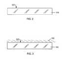
- FIG. 2is a simplified diagram illustrating a soda lime glass substrate provided for fabricating a thin film solar cell according to an embodiment of the present invention. This diagram is merely an example, which should not unduly limit the scope of the claims herein. One of ordinary skill in the art would recognize many variations, alternatives, and modifications.
- the soda lime glass substrate 100 including a surface region 101is provided.
- the soda lime glasscontains alkaline ions, for example greater 10 wt % sodium oxide, or about 15% wt % sodium.
- alkali-containing glass substratesare one of most widely used, inexpensive float window glasses, which are also widely used for forming thin film solar cells with low cost.
- One important reason for choosing the soda lime glass other than economical concernis to utilize its coefficient of thermal expansion of about 9.5 ppm/K, at ⁇ 25-600° C. that matches quite well with high efficiency thin film photovoltaic materials formed thereon.
- another reason for using the soda lime glass substrateis to utilize a positive influence from the alkaline ions (e.g., or simply sodium-bearing species) on the grain growth during the formation of the thin film photovoltaic materials.
- polycrystalline compound semiconductor chalcopyrite thin films of CuIn(Ga)Se 2 or CuInSe 2 materialscan be formed on soda lime glass substrates with coarse grain size of 1 microns or larger so that high cell current can be collected with these photovoltaic films with light-conversion efficiencies of 17% or above.
- certain metal or oxide thin filmis coated over the surface region.
- soda lime glass substrates used for this applicationthere is no such thin film coating.
- a surface treatmentis performed to the surface region of the soda lime glass substrate.
- the surface region 101 of the soda lime glass substrate 100is subjected to the treatment process 150 .
- the treatment process 150is a washing process carried out by soaking into a fluidic environment or simply rinsing with deionized (DI) water with resistivity between 0.05 & 1 Mega Ohm-cm and controlled PH-value above 6.0 to 7.0.
- the soda lime glass substratescan be treated for 15 to 30 minutes under ultrasonic duty in isopropyl alcohol, washed in DI water, and finally dried by blowing with dry nitrogen.
- the washing process 150substantially cleans the surface region 101 by removing surface contaminants, greases, dirt, dusts, and other particles with sizes greater than three microns.
- FIG. 4is a simplified diagram illustrating a barrier layer formed overlying the surface region of the soda lime glass substrate provided for fabricating a thin film solar cell according to an embodiment of the present invention. This diagram is merely an example, which should not unduly limit the scope of the claims herein. One of ordinary skill in the art would recognize many variations, alternatives, and modifications. As mentioned earlier, the grain growth of the photovoltaic materials on the soda lime glass substrate benefits from the existence of sodium-bearing species therein.
- a barrier layeris added overlying the surface region of the soda lime glass substrate for maintaining the sodium-bearing species within the substrate or at least not diffusing across the surface region during the formation of thin film solar cells. As shown in FIG. 4 , a thin barrier layer 200 is formed overlying the surface region 101 after a treatment process.
- the barrier layer 200is a silicon dioxide layer deposited using a sputtering process.
- an AC sputtering processcan be carried out in a chamber equipped with a silicon or silicon-aluminum tile target in an environment with injected oxygen gas at a controlled flow rate.
- Argon gasmay be provided for assisting the sputtering process at about a suitable flow rate.
- DC sputtering, e-beam evaporation, thermal/chemical deposition, sol-gel method, or any other suitable techniquescan be used.
- the AC sputtering processis performed with the soda lime glass substrate 100 being loaded into a vacuum chamber with a pressure of about 10 ⁇ 6 millitorr.
- the substrate temperatureis at a room temperature.
- the thickness of the thin barrier layer 200is about 200 Angstroms and greater. In another specific embodiment, the thickness of the barrier layer 200 is about 500 Angstroms and greater.
- silicon oxide, aluminum oxide, titanium nitride, silicon nitride, titanium oxide, or zirconium oxide or certain combination of above materialscan also be used as material for the thin barrier layer 200 .
- the barrier layer 200can be formed by sputtering from an aluminum doped silicon target. The deposition is done in argon gas plus oxygen gas mixture. About 200 to 500 Angstroms thick film can be deposited, containing a mixture of SiO 2 and Al 2 O 3 .
- barrier layer 200other materials like titanium oxide, SiON X , aluminum zinc oxide or a bi-layered film structure can be used for the barrier layer 200 .
- a two layer barriercan be deposited using following process. A first layer is deposited by sputtering on a target containing aluminum doped silicon. After that, a second layer is deposited using a pure silicon target.
- the carrier gascan be a mixture of argon and oxygen.
- the total thickness of the bi-layer barrier layercan be ranged from 200 to 2000 Angstroms.
- the methodfurther includes a process ( 1040 ) of forming a first molybdenum layer overlying the barrier layer.
- This processcan be visually illustrated by FIG. 5 .
- FIG. 5is a simplified diagram illustrating a first molybdenum layer formed overlying the barrier layer according to an embodiment of the present invention. This diagram is merely an example, which should not unduly limit the scope of the claims herein. One of ordinary skill in the art would recognize many variations, alternatives, and modifications.
- the first molybdenum layer 305is formed, using a first process, overlying the barrier layer 200 .
- the first molybdenum layeris a part of a bi-layered film formed in a first part of a complete metal deposition process.
- the first processis a low-pressure molybdenum sputtering process carried out in a compartment with a pressure of about 1 to 5 millitorr, leading to the first molybdenum layer 305 with a thickness of about 200 Angstroms to 700 Angstroms.
- this sputtering compartment for forming the first molybdenum layer 305can be in a single chamber, but different compartment, as that for forming the barrier layer 200 .
- the first processis designed to provide the first molybdenum layer characterized as a film in substantial tensile stress.
- the first molybdenum layer 305can be formed under tensile stress ranging from 300 MPa to 1000 MPa overlying the barrier layer 200 .
- the tensile stress within the first molybdenum layer 305is configured to allow removal of the first molybdenum layer 305 via laser ablation for patterning from an underlying transparent substrate 100 (with a barrier layer 200 ).
- the tensile stress of the remaining portion of the first molybdenum layer 305helps the remaining portion being strongly attached with the substrate 100 with the overlying barrier layer 200 . More descriptions on the functional effect of the first molybdenum layer 305 during a patterning process of forming a lower electrode layer can be found in later paragraphs of the specification. Of course, there can be other variations, modifications, and alternatives.
- the method 1000includes forming a second molybdenum layer on the first molybdenum layer.
- This processcan be visually illustrated by FIG. 6 .
- FIG. 6is a simplified diagram illustrating a second molybdenum layer formed overlying the first molybdenum layer according to an embodiment of the present invention. This diagram is merely an example, which should not unduly limit the scope of the claims herein. One of ordinary skill in the art would recognize many variations, alternatives, and modifications. As shown, a bi-layer structure is formed with the second molybdenum layer 308 overlying the first molybdenum layer 305 .
- the second molybdenum layer 308is formed in a second process, or a second part of a complete metal deposition process.
- the second processis a relative high-pressure molybdenum sputtering process carried out in a compartment with a pressure between 10 millitorr and 20 millitorr, leading to the second molybdenum layer 308 with a thickness of about 2000 Angstroms to 7000 Angstroms.
- the second molybdenum layer 308is formed under compressive stress ranging from stress neutral to ⁇ 200 MPa, overlying the first molybdenum layer 305 .
- the compressive stress within the second molybdenum layer 308is configured to facilitate a self repairing of the film cracking or thin-edge-void within the first molybdenum layer 305 around the patterns formed during the laser ablation patterning process. Further details about the functional effect of the compressive second molybdenum layer over a tensile first molybdenum layer can be found in later paragraphs of the specification.
- the bi-layer electrode processcan be done using following optional conditions.
- the process 1040 for forming the first molybdenum layercan be done at a low pressure of around 1-5 mtorr and a lower sputtering power of about 1-4 kW.
- the subsequent process ( 1050 ) for forming the second molybdenum layeruses high pressure about 10-20 mtorr combined with high sputtering power of about 12-18 kW.
- the thickness of each layercan be similar to that described above.
- Other options of the processing conditionscan be utilized. For example, the pressure of the chamber can be kept constant for both sputtering processes.
- the sputtering powercan be set to low at 1-4 kW for the first molybdenum layer and increased to high at about 12-18 kW for the second molybdenum layer.
- the first layercan be deposited at low power but relative high pressure and the second layer at high power but relative low pressure.
- the stress nature of the bi-layer film structureis modified but the first layer still is in tensile and the second layer in compressive.
- the first molybdenum layercan be replaced by another material such as titanium.
- the thickness of the titanium layeris about 300 Angstroms.
- a titanium under layercan be added before the first molybdenum layer is formed.
- the methodincludes a process ( 1060 ) of patterning the first molybdenum layer and the second molybdenum layer to form a lower electrode layer.
- This processcan be visually illustrated by FIG. 7 .
- FIG. 7is a simplified diagram illustrating a lower electrode layer formed with a pattern according to an embodiment of the present invention. This diagram is merely an example, which should not unduly limit the scope of the claims herein. One of ordinary skill in the art would recognize many variations, alternatives, and modifications.
- a pattern 310is formed as a via with a depth through both the first molybdenum layer 305 and the second molybdenum layer 308 .
- the patterning process 1060is a process utilizing an electromagnetic radiation 350 to form the pattern 310 by controllably removing a certain amount of the second molybdenum layer and the first molybdenum layer from the barrier layer 200 overlying the substrate 100 .
- the electromagnetic radiation 350can be a laser beam generated from a laser source based on Q-switched Nd: YAG infrared laser. Other laser with similar medium or frequency-doubled green laser can also be used.
- the pattern 310can have a width of about 20 to 50 micron.
- FIGS. 7A through 7Eare schematic diagrams showing a functional effect of the bi-layered electrode layer for fabricating thin film solar cell according to an embodiment of the present invention. These diagrams are merely examples which should not unduly limit the scope of the claims herein. One of ordinary skill in the art would recognize many variations, alternatives, and modifications.
- a side view of the filmillustrate a tensile first molybdenum layer 305 covered by a compressive second molybdenum layer 308 , formed on a barrier layer 200 over the substrate 100 .
- the tensile stress in the first molybdenum layer 305tends to shrink the film while the compressive stress in the second molybdenum layer 308 tends to expand the film.
- a laser beam 350 applied from above the second molybdenum layer 308injects energy into the bi-layer molybdenum film.
- the first molybdenum layer 305 under the laser beam 350absorb (at least partially) the injected energy, the existed tensile stress helps to shrink the film (under the beam) to form a loosed portion 3105 of the first molybdenum layer 305 .
- the loosed portion 3105becomes removable from the underneath barrier layer 200 .
- the materials within the portion 3105 and 3108can be removed away from the barrier layer 200 , as indicated by the arrow, to form a pattern 310 .
- FIG. 7Dshows a top view of the formed pattern 310 , specifically showing a likely structure within a plane in the first molybdenum layer 305 . Due to the existing tensile stress, the remaining portion of the first molybdenum layer 305 surrounding the pattern 310 still tends to shrink, which may cause formations of several cracks or voids 3115 near edges of the pattern 310 . The edges of the remaining portion of the first molybdenum layer 305 near those cracks or voids 3115 may even become partially peeled off, capable of causing shunts or other degradations for subsequent layers if not being repaired.
- Embodiments of the present inventionintroduce a self-repairing mechanism using the compressive second molybdenum layer 308 over the first molybdenum layer 305 during the patterning process to form the lower electrode layer.
- the compressive stress in the remaining portion of the second molybdenum layer 308 around the pattern 310tends to automatically expand at the same time as the first molybdenum layer 305 tends to form those cracks 3115 .
- FIG. 7E of a plane view of the same pattern 310 surrounded by the second molybdenum layer 308no cracks are seen around the pattern edge and elsewhere.
- any cracks formed in the first molybdenum layer 305are effectively repaired or filled by expanding second molybdenum layer 308 .
- the rest portion of the first molybdenum layer 305covered by corresponding remaining portion of the second molybdenum layer 308 , is still in tensile stress that helps to hold the film tightly onto the barrier layer 200 . Therefore, the specific bi-layer structure associated with the first molybdenum layer and the second molybdenum layer and corresponding tensile/compressive stress configuration successfully reduce film cracking during the patterning process that leads to a formation of a lower electrode layer for the thin film solar cell to be formed later.
- the formed pattern by the process 1060is substantially free from the random voids, cracks, berms of sizes smaller than 0.1 microns.
- the patterned electrode layer 300 including both the first molybdenum layer and the second molybdenum layercan serve as an upper electrode layer for a top solar cell.
- the upper electrode layerneeds to be optically transparent.
- molybdenum layer with thickness of about 0.5 microns or lessit is optically transparent to visible light.
- transparent conductive oxidecan be used as the material for the upper electrode layer.
- FIG. 8is a simplified diagram illustrating a layer of photovoltaic material formed overlying the lower electrode layer for fabricating a thin film solar cell on soda lime glass according to an embodiment of the present invention. This diagram is merely an example, which should not unduly limit the scope of the claims herein. One of ordinary skill in the art would recognize many variations, alternatives, and modifications. As shown, the layer of photovoltaic material 400 is applied on the lower electrode layer 300 .
- the layer of photovoltaic materialis a multilayered structure that is formed by a series of thin film deposition, anneal treatment, etching treatment, mechanical or laser patterning, doping or implantation, and other suitable processes.
- the layer of photovoltaic material 400can be formed by a sputtering process using a copper-gallium alloy target and an indium target with a atomic purity up to 99%.
- the sputtering processincludes multi-steps, each step with predominantly one type of material (either copper or indium) being deposited, carried out in a separate compartment within a single chamber at a temperature of about 500 degree Celsius.
- a conductive materialcan be filled into the pattern 310 to form an interconnect structure 311 within the lower electrode layer 300 before or during the formation of the layer of photovoltaic material 400 .
- the sputtering processcan be replaced by other techniques including vacuum evaporation, plating, chemical vapor deposition, or chemical bath deposition.
- the sputtering processis followed by or substantially carried out at the same time with a sodium-bearing species coating process to add a desired amount of sodium-bearing species or other alkaline ions into the films.
- a sodium-bearing species coating processto add a desired amount of sodium-bearing species or other alkaline ions into the films.
- the copper-indium materials (or copper indium gallium materials) deposited earlier plus the desired amount of sodium-bearing speciescan be treated by a thermal process under a specific environment including selenide (or sulfide in certain embodiment) in fluidic phase, leading to a selenization process to form a film of copper indium (gallium) diselenide compound with crystal grains in substantially chalcopyrite structure.
- the film of copper indium(gallium)diselenide (CIS or CIGS) in chalcopyrite structurebecomes a photovoltaic absorber layer for fabricating a thin film solar cell.
- the barrier layer 200formed at Process 1030
- the sodium content within the soda lime glass substrate 100is substantially maintained with the substrate thereof at elevated processing temperatures. Therefore, the method 1000 according to embodiments of the present invention ensures no uncontrolled sodium-bearing species are introduced into the films formed above the surface region of the soda lime glass substrate.
- this barrier layer 200also advantageously prevents excessive sodium from causing a reactive injury to the lower electrode layer 300 made by molybdenum material.
- the photovoltaic material in the multilayered structurefunctionally can include at least one absorber layer and one window layer overlying the absorber layer, serving as basic solar cell elements for collecting sun light and converting into electricity.
- the absorber layer 405can be the thin film in chalcopyrite structure made by copper indium(gallium)diselenide (CIS or CIGS) compound material.
- the absorber layer 405can be a copper indium gallium disulfide compound semiconductor material or copper indium disulfide compound semiconductor material.
- the absorber layer 405usually is characterized as a p-type semiconductor through one or more doping process. Typically p-type acceptor dopants include boron or aluminum ions.
- the absorber layer 405 mentioned abovecan be produced by sputtering, plating, evaporation, and other suitable deposition plus the selenization or sulfurization and one or more thermal processes.
- sputteringplating, evaporation, and other suitable deposition plus the selenization or sulfurization and one or more thermal processes.
- other specific CIS and/or CIGS configurationscan also be used, such as those noted in U.S. Pat. No. 4,612,411 and U.S. Pat. No. 4,611,091, which are hereby incorporated by reference herein, without departing from the invention described by the claims herein.
- the absorber layer 405is overlaid by a window layer 408 characterized as a wide bandgap semiconductor with a photovoltaic junction.
- the window layercan be selected from a group materials consisting of a cadmium sulfide (CdS), a zinc sulfide (ZnS), zinc selenium (ZnSe), zinc oxide (ZnO), zinc magnesium oxide (ZnMgO), or others and may be doped with impurities for conductivity, e.g., n′-type. Sputtering, vacuum evaporation, and chemical bath deposition (CBD) techniques are widely used for the formation of the window layer.
- CBDchemical bath deposition
- CBDis an inexpensive and convenient method for large-area preparation of thin window layer at close-to-room temperatures, where a controllable chemical reaction in an aqueous solution, containing the various reactants, is involved.
- indium speciesare used as the doping element to cause formation of the n + -type semiconductor characteristic.
- the absorber layer 405 resulted from the above processesis about 1 to 10 microns in thickness, but can be other dimensions.
- the window layer 408usually is thinner than the absorber layer 405 .
- a window layer 408 of CdS material made by a CBD methodcan have a thickness ranging from about 200 to 500 nanometers.
- the methodfurther includes a process ( 1080 ) of forming a first zinc oxide layer overlying the layer of photovoltaic material.
- FIG. 10is a simplified diagram illustrating a first zinc oxide layer formed over the layer of photovoltaic material for fabricating a thin film solar cell on soda lime glass according to an embodiment of the present invention. This diagram is merely an example, which should not unduly limit the scope of the claims herein. One of ordinary skill in the art would recognize many variations, alternatives, and modifications.
- the first zinc oxide layer 500forms overlying the layer of photovoltaic material 400 that is formed in previous process ( 1070 ).
- the first zinc oxide layer 500includes an interconnect structure 511 that can be formed by a patterning process carried out after the Process 1080 .
- the first zinc oxide layer 500serves as an upper (or front) electrode layer for the thin film solar cell formed on the soda lime glass substrate.
- the first zinc oxide layer 500can be a properly n-type doped to make it electrically conductive.
- the n-type dopingis possible by introduction of boron, aluminum, indium, or excess zinc.
- the zinc oxideis optically transparent as a so-called transparent conducting oxide (TCO) material and often used in thin film solar devices.
- TCOtransparent conducting oxide
- Other materialsfor example, Indium tin oxide (ITO) and fluorine doped tin oxide (TFO) can also be used.
- the first zinc oxide layeris formed using a metalorganic chemical vapor deposition (MOCVD) technique within a batch system.
- MOCVDmetalorganic chemical vapor deposition
- the formed first zinc oxide layer by MOCVDis a rough layer, which can diffuse the incoming light by scattering, increasing the efficiency of solar cells.
- the first zinc oxide layeris formed over the window layer overlying the copper indium diselenide absorber layer of the photovoltaic material.
- the window layer 408is a cadmium sulfide layer formed using the CBD technique. The cadmium sulfide layer can be deposited after the formation of the copper indium diselenide absorber layer or the copper indium gallium diselenide absorber layer.
- FIG. 11is a simplified diagram illustrating a second zinc oxide layer formed overlying the layer of photovoltaic material before the formation of the first zinc oxide layer according to an alternative embodiment of the present invention.
- This diagramis merely an example, which should not unduly limit the scope of the claims herein.
- the second zinc oxide layer 505is sandwiched between the first zinc oxide layer 500 and the layer of photovoltaic material 400 .
- the second zinc oxide layer 505has a higher resistivity than the first zinc oxide layer 500 .
- the methodincludes performing other processes ( 1090 ).
- forming a second zinc oxide layeris one optional process 1090 .
- FIG. 12is a simplified diagram illustrating one or more layers formed according to certain embodiments of the invention. This diagram is merely an example, which should not unduly limit the scope of the claims herein.
- a layered structureincluding the soda lime glass substrate 100 , the barrier layer 200 , the first electrode layer 300 , the layer of photovoltaic material 400 , and the first zinc oxide layer (or the second electrode layer) creates a basic structure for fabricating a first thin film solar cell.
- one or more layers 600can be provided (or assembled) over the top of the first thin film solar cell, i.e., over the first zinc oxide layer 500 of the above layered structure.
- the added one or more layers 600simply can be a second thin film solar cell formed by similar method while using a soda lime glass superstrate.
- the one or more layers 600represent another copper indium diselenide layer sandwiched by transparent electrode layers with proper patterned interconnect structures to form a photovoltaic cell structure.
- the other processes 1090can include forming the second solar cell including the one or more layers 600 and assembling the second thin film solar cell with the first thin film solar cell to form a multi-junction module.
- FIGS. 13 and 14are tested IV characteristics of thin film solar modules fabricated according to embodiments of the present invention.
- FIG. 13shows an IV characteristic of a thin film solar module of 20 cm ⁇ 20 cm made on a soda lime glass substrate according to an embodiment of the present invention.
- the solar cellhas a bi-layered electrode formed on a barrier layer overlying the glass substrate.
- the barriercan be any of those noted, but can be others.
- the bi-layered electrodecomprises a first molybdenum (Mo) layer in tensile stress configuration and a second molybdenum layer in compressive stress overlying the first Mo layer according to this example.
- Momolybdenum
- the first Mo layeris formed by sputtering Mo target at low pressure of about 2 mtorr and low power of 1-4 kW.
- the second Mo layeris formed by sputtering Mo target at high pressure of about 20 mtorr and high power of 12-18 kW.
- the short circuit current I sc of the moduleis about 0.35 A and the open circuit voltage V oc is about 13.91 Volt.
- the module efficiencyis about 11%.
- FIG. 14shows an IV characteristic of another thin film solar module of 20 cm ⁇ 20 cm made on a soda lime glass substrate according to an embodiment of the present invention.
- This cellhas a Mo bi-layer electrode film overlying a barrier layer on the substrate.
- the barriercan be any of those noted, but can be others.
- the process condition for this bi-layer Mo electrodeis at a constant pressure for both layers of the bi-layer structure but the first Mo layer is done with a lower power with the second Mo layer is done with a higher power.
- the short circuit of the moduleis measured to be 0.34 A and the open circuit voltage of the module is about 14 V.
- the module efficiencyis about 10.5%.
Landscapes
- Photovoltaic Devices (AREA)
Abstract
Description
- This application claims priority to U.S. Provisional Patent Application No. 61/101,645, filed Sep. 30, 2008, entitled “THIN FILM SODIUM SPECIES BARRIER METHOD AND STRUCTURE FOR CIGS BASED THIN FILM PHOTOVOLTAIC CELL” by inventor Robert D. Wieting, commonly assigned and incorporated by reference herein for all purposes.
- NOT APPLICABLE
- NOT APPLICABLE
- The present invention relates generally to photovoltaic materials and manufacturing method. More particularly, the present invention provides a method and structure for fabricating thin film solar cells. Merely by way of example, the present method and structure for manufacture of copper indium gallium diselenide based thin film photovoltaic devices, but it would be recognized that the invention may have other configurations.
- From the beginning of time, mankind has been challenged to find way of harnessing energy. Energy comes in the forms such as petrochemical, hydroelectric, nuclear, wind, biomass, solar, and more primitive forms such as wood and coal. Over the past century, modern civilization has relied upon petrochemical energy as an important energy source. Petrochemical energy includes gas and oil. Gas includes lighter forms such as butane and propane, commonly used to heat homes and serve as fuel for cooking Gas also includes gasoline, diesel, and jet fuel, commonly used for transportation purposes. Heavier forms of petrochemicals can also be used to heat homes in some places. Unfortunately, the supply of petrochemical fuel is limited and essentially fixed based upon the amount available on the planet Earth. Additionally, as more people use petroleum products in growing amounts, it is rapidly becoming a scarce resource, which will eventually become depleted over time.
- More recently, environmentally clean and renewable sources of energy have been desired. An example of a clean source of energy is hydroelectric power. Hydroelectric power is derived from electric generators driven by the flow of water produced by dams such as the Hoover Dam in Nevada. The electric power generated is used to power a large portion of the city of Los Angeles in California. Clean and renewable sources of energy also include wind, waves, biomass, and the like. That is, windmills convert wind energy into more useful forms of energy such as electricity. Still other types of clean energy include solar energy. Specific details of solar energy can be found throughout the present background and more particularly below.
- Solar energy technology generally converts electromagnetic radiation from the sun to other useful forms of energy. These other forms of energy include thermal energy and electrical power. For electrical power applications, solar cells are often used. Although solar energy is environmentally clean and has been successful to a point, many limitations remain to be resolved before it becomes widely used throughout the world. As an example, one type of solar cell uses crystalline materials, which are derived from semiconductor material ingots. These crystalline materials can be used to fabricate optoelectronic devices that include photovoltaic and photodiode devices that convert electromagnetic radiation into electrical power. However, crystalline materials are often costly and difficult to make on a large scale. Additionally, devices made from such crystalline materials often have low energy conversion efficiencies. Other types of solar cells use “thin film” technology to form a thin film of photosensitive material to be used to convert electromagnetic radiation into electrical power. Similar limitations exist with the use of thin film technology in making solar cells. That is, efficiencies are often poor. Additionally, film reliability is often poor and cannot be used for extensive periods of time in conventional environmental applications. Often, thin films are difficult to mechanically integrate with each other. Furthermore, integration of electrode layers, sodium-containing glass substrates, and overlying absorber layers was also problematic. These and other limitations of these conventional technologies can be found throughout the present specification and more particularly below.
- The present invention relates generally to photovoltaic materials and manufacturing method. More particularly, the present invention provides a method and structure for fabricating thin film solar cells. Merely by way of example, the present method and structure for manufacture of copper indium gallium diselenide based thin film photovoltaic devices, but it would be recognized that the invention may have other configurations.
- In a specific embodiment, the present invention provides a method for fabricating a thin film solar cell. The method includes providing a soda lime glass substrate comprising a surface region and a concentration of sodium oxide of greater than about 10 percent by weight. The method further includes treating the surface region with one or more cleaning process, using a deionized water rinse, to remove surface contaminants having a particles size of greater than three microns. Additionally, the method includes process of forming a barrier layer overlying the surface region. The barrier layer is characterized to maintain the sodium within the soda lime glass substrate. The method further includes a first process of forming a first molybdenum layer overlying the barrier layer. The first molybdenum layer has a first thickness and is in tensile configuration. The method also includes a second process of forming a second molybdenum layer overlying the first molybdenum layer. The second molybdenum layer has a second thickness, which is greater than the first thickness, and is in compressive configuration. Furthermore, the method includes patterning the first molybdenum layer and the second molybdenum layer to form a lower electrode layer. Moreover, the method includes forming a layer of photovoltaic material overlying the lower electrode layer and forming a first zinc oxide layer overlying the layer of photovoltaic materials.
- In another specific embodiment, the present invention provides a method for fabricating a thin film solar cell. The method includes providing a soda lime glass substrate comprising a surface region and a concentration of sodium oxide of greater than about 10 percent by weight. The method further includes forming a barrier layer overlying the surface region. The barrier layer is characterized to maintain sodium within the soda lime glass substrate. Additionally, the method includes forming a first molybdenum layer using a first process overlying the barrier layer. The first molybdenum layer has a first thickness and is in tensile configuration. The method also includes forming a second molybdenum layer using a second process overlying the first molybdenum layer. The second molybdenum layer has a second thickness, which is greater than the first thickness, and is in compressive configuration. Furthermore, the method includes patterning the first molybdenum layer and the second molybdenum layer to form a lower electrode layer. Moreover, the method includes forming an absorber material comprising a copper species, a gallium species, an indium species, and a selenium species overlying the lower electrode layer and forming a first zinc oxide layer overlying the absorber material.
- In an alternative embodiment, the present invention provides a thin film solar cell device. The thin film solar cell device includes a soda lime glass substrate comprising a surface region and a concentration of sodium oxide of greater than about 10 percent by weight. The thin film solar cell device further includes a barrier layer overlying the surface region to maintain the sodium within the soda lime glass substrate. Additionally, the thin film solar cell device includes a lower electrode layer comprising a first molybdenum layer overlying the barrier layer and a second molybdenum layer overlying the first molybdenum layer. The first molybdenum layer has a first thickness and is in tensile configuration, and the second molybdenum layer has a second thickness, which is greater than the first thickness, and is in compressive configuration. Furthermore, the thin film solar cell device includes an absorber material comprising a copper species, an indium species, a gallium species, and a selenium species overlying the lower electrode layer and a first zinc oxide layer overlying the absorber material.
- In certain specific embodiments, the photovoltaic absorber layer is a copper indium diselenide compound semiconductor film in chalcopyrite structure or a copper indium gallium diselenide material. In some other embodiments, the absorber layer is covered by a window layer with wide band gap or different dopings. The window layer can be cadmium sulfide (CdS), a zinc sulfide (ZnS), zinc selinium (ZnSe), zinc oxide (ZnO), zinc magnesium oxide (ZnMgO), or others. In yet other embodiments, the first zinc oxide layer, served as the upper electrode layer of the thin film solar cell device, can be formed after a formation of a second zinc oxide layer over the absorber layer. In particular, the second zinc oxide layer has a higher resistivity than the first zinc oxide layer.
- Many benefits can be achieved by applying the embodiments of the present invention. Particularly, a thin barrier layer serves an important diffusion barrier for keeping sodium-bearing species within the soda lime glass substrate used for forming a thin film photovoltaic cell. The barrier layer prevents uncontrolled excessive sodium to react with molybdenum electrode layer or causing film grain degradation during formation of a film of copper indium diselenide in chalcopyrite structure with large grain sizes for achieving high efficiency of thin film solar cells thereof. Embodiments of the invention also include forming a bi-layered molybdenum electrode layer with specific layered compressive/tensile stress and thickness control through a process control. Accordingly the bi-layered electrode layer is particularly suitable for laser patterning to form a desired lower electrode layer for fabricating a thin film solar cell. Of course, there can be other variations, modifications, and alternatives.
- These and other benefits may be described throughout the present specification and more particularly below.
FIG. 1 is a simplified flowchart illustrating a method of fabricating a thin film solar cell according to an embodiment of the present invention;FIGS. 2-7 ,7A-7E, and8-12 are schematic diagrams illustrating a method comprising a series of steps for fabricating a thin film solar cell according to certain embodiments of the present invention; andFIGS. 13 and 14 are tested IV characteristics of thin film solar modules fabricated according to embodiments of the present invention.- The present invention relates generally to photovoltaic materials and manufacturing method. More particularly, the present invention provides a method and structure for fabricating thin film solar cells. Merely by way of example, the present method and structure for manufacture of copper indium gallium diselenide based thin film photovoltaic devices, but it would be recognized that the invention may have other configurations.
FIG. 1 is a simplified flowchart illustrating a method of fabricating a thin film solar cell according to an embodiment of the present invention. This diagram is merely an example, which should not unduly limit the scope of the claims herein. Themethod 1000 includes the following processes:- 1.
Process 1010 for providing a soda lime glass substrate with a surface region; - 2.
Process 1020 for treating the surface region; - 3.
Process 1030 for forming a barrier layer overlying the surface region; - 4.
Process 1040 for forming a first molybdenum layer, using a first process, overlying the barrier layer; - 5.
Process 1050 for forming a second molybdenum layer, using a second process, overlying the first molybdenum layer; - 6.
Process 1060 for patterning the first molybdenum layer and the second molybdenum layer to form a lower electrode layer; - 7.
Process 1070 for forming a layer of photovoltaic material overlying the lower electrode layer; - 8.
Process 1080 for forming a first zinc oxide layer overlying the layer of photovoltaic material; - 9.
Process 1090 for performing other steps.
- 1.
- The above sequence of processes provides a method of using a thin film barrier structure in processes for manufacture of thin film solar cells according to an embodiment of the present invention. The method is applied to the copper indium gallium diselenide based thin film photovoltaic cell. Other alternatives can also be provided where processes are added, one or more processes are removed, or one or more processes are provided in a different sequence without departing from the scope of the claims herein. For example, forming the layer of photovoltaic material may include formation of a multiple layered structure involving many processes including deposition, annealing, etching, patterning, doping, and so on. In another example, the formation of the first zinc oxide layer may be carried out after a formation of a second zinc oxide layer overlying the layer of photovoltaic material, the second zinc oxide having different electric property from the first zinc oxide layer. Further details of the method can be found throughout the present specification and more particularly below.
- At
Process 1010, a soda lime glass substrate is provided. This process can be visually illustrated byFIG. 2 .FIG. 2 is a simplified diagram illustrating a soda lime glass substrate provided for fabricating a thin film solar cell according to an embodiment of the present invention. This diagram is merely an example, which should not unduly limit the scope of the claims herein. One of ordinary skill in the art would recognize many variations, alternatives, and modifications. As shown, the sodalime glass substrate 100 including asurface region 101 is provided. In one embodiment, the soda lime glass contains alkaline ions, for example greater 10 wt % sodium oxide, or about 15% wt % sodium. It has been known that alkali-containing glass substrates are one of most widely used, inexpensive float window glasses, which are also widely used for forming thin film solar cells with low cost. One important reason for choosing the soda lime glass other than economical concern is to utilize its coefficient of thermal expansion of about 9.5 ppm/K, at ˜25-600° C. that matches quite well with high efficiency thin film photovoltaic materials formed thereon. In addition, another reason for using the soda lime glass substrate is to utilize a positive influence from the alkaline ions (e.g., or simply sodium-bearing species) on the grain growth during the formation of the thin film photovoltaic materials. For example, polycrystalline compound semiconductor chalcopyrite thin films of CuIn(Ga)Se2or CuInSe2materials can be formed on soda lime glass substrates with coarse grain size of 1 microns or larger so that high cell current can be collected with these photovoltaic films with light-conversion efficiencies of 17% or above. On some commercial soda lime glass substrates, certain metal or oxide thin film is coated over the surface region. On some soda lime glass substrates used for this application, there is no such thin film coating. - At
Process 1020, a surface treatment is performed to the surface region of the soda lime glass substrate. As shown inFIG. 3 , thesurface region 101 of the sodalime glass substrate 100 is subjected to thetreatment process 150. In one embodiment, thetreatment process 150 is a washing process carried out by soaking into a fluidic environment or simply rinsing with deionized (DI) water with resistivity between 0.05 & 1 Mega Ohm-cm and controlled PH-value above 6.0 to 7.0. In one example, the soda lime glass substrates can be treated for 15 to 30 minutes under ultrasonic duty in isopropyl alcohol, washed in DI water, and finally dried by blowing with dry nitrogen. Thewashing process 150 substantially cleans thesurface region 101 by removing surface contaminants, greases, dirt, dusts, and other particles with sizes greater than three microns. - At next process (1030), the method includes forming a barrier layer overlying the surface region. This process can be visually illustrated by
FIG. 4 .FIG. 4 is a simplified diagram illustrating a barrier layer formed overlying the surface region of the soda lime glass substrate provided for fabricating a thin film solar cell according to an embodiment of the present invention. This diagram is merely an example, which should not unduly limit the scope of the claims herein. One of ordinary skill in the art would recognize many variations, alternatives, and modifications. As mentioned earlier, the grain growth of the photovoltaic materials on the soda lime glass substrate benefits from the existence of sodium-bearing species therein. However, it has been known that excessive supply of sodium-bearing species from the soda lime glass substrate would cause degradation of the crystallographic grain structure and correspondingly reduction of cell current, no-load voltage, or short-circuit current density, and other properties important for high efficiency solar cells. Especially during the photovoltaic thin film formation process on a heated substrate the sodium-bearing species inside the substrate would easily diffuse into the films overlying the substrate without control. In one example, instead of replacing the soda lime glass substrate with a non-sodium-bearing substrate, a barrier layer is added overlying the surface region of the soda lime glass substrate for maintaining the sodium-bearing species within the substrate or at least not diffusing across the surface region during the formation of thin film solar cells. As shown inFIG. 4 , athin barrier layer 200 is formed overlying thesurface region 101 after a treatment process. - The
barrier layer 200 is a silicon dioxide layer deposited using a sputtering process. For example, an AC sputtering process can be carried out in a chamber equipped with a silicon or silicon-aluminum tile target in an environment with injected oxygen gas at a controlled flow rate. In one implementation, Argon gas may be provided for assisting the sputtering process at about a suitable flow rate. In other implementations, DC sputtering, e-beam evaporation, thermal/chemical deposition, sol-gel method, or any other suitable techniques can be used. In a preferred embodiment, the AC sputtering process is performed with the sodalime glass substrate 100 being loaded into a vacuum chamber with a pressure of about 10−6millitorr. The substrate temperature is at a room temperature. In a specific embodiment, the thickness of thethin barrier layer 200 is about 200 Angstroms and greater. In another specific embodiment, the thickness of thebarrier layer 200 is about 500 Angstroms and greater. In certain embodiments, silicon oxide, aluminum oxide, titanium nitride, silicon nitride, titanium oxide, or zirconium oxide or certain combination of above materials can also be used as material for thethin barrier layer 200. For example, thebarrier layer 200 can be formed by sputtering from an aluminum doped silicon target. The deposition is done in argon gas plus oxygen gas mixture. About 200 to 500 Angstroms thick film can be deposited, containing a mixture of SiO2and Al2O3. - In an alternative embodiment, other materials like titanium oxide, SiONX, aluminum zinc oxide or a bi-layered film structure can be used for the
barrier layer 200. For example, a two layer barrier can be deposited using following process. A first layer is deposited by sputtering on a target containing aluminum doped silicon. After that, a second layer is deposited using a pure silicon target. The carrier gas can be a mixture of argon and oxygen. The total thickness of the bi-layer barrier layer can be ranged from 200 to 2000 Angstroms. - Referring to
FIG. 1 , the method further includes a process (1040) of forming a first molybdenum layer overlying the barrier layer. This process can be visually illustrated byFIG. 5 .FIG. 5 is a simplified diagram illustrating a first molybdenum layer formed overlying the barrier layer according to an embodiment of the present invention. This diagram is merely an example, which should not unduly limit the scope of the claims herein. One of ordinary skill in the art would recognize many variations, alternatives, and modifications. As shown, thefirst molybdenum layer 305 is formed, using a first process, overlying thebarrier layer 200. In one embodiment, the first molybdenum layer is a part of a bi-layered film formed in a first part of a complete metal deposition process. The first process is a low-pressure molybdenum sputtering process carried out in a compartment with a pressure of about 1 to 5 millitorr, leading to thefirst molybdenum layer 305 with a thickness of about 200 Angstroms to 700 Angstroms. In one implementation, this sputtering compartment for forming thefirst molybdenum layer 305 can be in a single chamber, but different compartment, as that for forming thebarrier layer 200. In another embodiment, the first process is designed to provide the first molybdenum layer characterized as a film in substantial tensile stress. Depending also on the sputtering power and substrate temperature, other than the low-pressure condition, thefirst molybdenum layer 305 can be formed under tensile stress ranging from 300 MPa to 1000 MPa overlying thebarrier layer 200. Of course, other stress levels can also be used depending upon the embodiment. In a preferred embodiment, the tensile stress within thefirst molybdenum layer 305 is configured to allow removal of thefirst molybdenum layer 305 via laser ablation for patterning from an underlying transparent substrate100 (with a barrier layer200). The tensile stress of the remaining portion of thefirst molybdenum layer 305 helps the remaining portion being strongly attached with thesubstrate 100 with theoverlying barrier layer 200. More descriptions on the functional effect of thefirst molybdenum layer 305 during a patterning process of forming a lower electrode layer can be found in later paragraphs of the specification. Of course, there can be other variations, modifications, and alternatives. - In a subsequent process (1050), the
method 1000 includes forming a second molybdenum layer on the first molybdenum layer. This process can be visually illustrated byFIG. 6 .FIG. 6 is a simplified diagram illustrating a second molybdenum layer formed overlying the first molybdenum layer according to an embodiment of the present invention. This diagram is merely an example, which should not unduly limit the scope of the claims herein. One of ordinary skill in the art would recognize many variations, alternatives, and modifications. As shown, a bi-layer structure is formed with thesecond molybdenum layer 308 overlying thefirst molybdenum layer 305. In particular, thesecond molybdenum layer 308 is formed in a second process, or a second part of a complete metal deposition process. The second process is a relative high-pressure molybdenum sputtering process carried out in a compartment with a pressure between 10 millitorr and 20 millitorr, leading to thesecond molybdenum layer 308 with a thickness of about 2000 Angstroms to 7000 Angstroms. Depending on the pressure and also on sputtering power and temperature, thesecond molybdenum layer 308 is formed under compressive stress ranging from stress neutral to −200 MPa, overlying thefirst molybdenum layer 305. In a preferred embodiment, the compressive stress within thesecond molybdenum layer 308 is configured to facilitate a self repairing of the film cracking or thin-edge-void within thefirst molybdenum layer 305 around the patterns formed during the laser ablation patterning process. Further details about the functional effect of the compressive second molybdenum layer over a tensile first molybdenum layer can be found in later paragraphs of the specification. - In an alternative embodiment, the bi-layer electrode process can be done using following optional conditions. For example, the
process 1040 for forming the first molybdenum layer can be done at a low pressure of around 1-5 mtorr and a lower sputtering power of about 1-4 kW. The subsequent process (1050) for forming the second molybdenum layer uses high pressure about 10-20 mtorr combined with high sputtering power of about 12-18 kW. The thickness of each layer can be similar to that described above. Other options of the processing conditions can be utilized. For example, the pressure of the chamber can be kept constant for both sputtering processes. But the sputtering power can be set to low at 1-4 kW for the first molybdenum layer and increased to high at about 12-18 kW for the second molybdenum layer. Of course, there can be other variations, modifications, and alternatives. For example, the first layer can be deposited at low power but relative high pressure and the second layer at high power but relative low pressure. The stress nature of the bi-layer film structure is modified but the first layer still is in tensile and the second layer in compressive. Alternatively, the first molybdenum layer can be replaced by another material such as titanium. The thickness of the titanium layer is about 300 Angstroms. Furthermore, a titanium under layer can be added before the first molybdenum layer is formed. - Referring to
FIG. 1 again, the method includes a process (1060) of patterning the first molybdenum layer and the second molybdenum layer to form a lower electrode layer. This process can be visually illustrated byFIG. 7 .FIG. 7 is a simplified diagram illustrating a lower electrode layer formed with a pattern according to an embodiment of the present invention. This diagram is merely an example, which should not unduly limit the scope of the claims herein. One of ordinary skill in the art would recognize many variations, alternatives, and modifications. As shown schematically, apattern 310 is formed as a via with a depth through both thefirst molybdenum layer 305 and thesecond molybdenum layer 308. Here thepattern 310 is simplified as a rectangular shape having a width and a depth while other more complicated shapes can be formed or used depending on applications. In one implementation, thepatterning process 1060 is a process utilizing anelectromagnetic radiation 350 to form thepattern 310 by controllably removing a certain amount of the second molybdenum layer and the first molybdenum layer from thebarrier layer 200 overlying thesubstrate 100. In particular, theelectromagnetic radiation 350 can be a laser beam generated from a laser source based on Q-switched Nd: YAG infrared laser. Other laser with similar medium or frequency-doubled green laser can also be used. In one example, under a beam spot of the laser radiation350 a portion thesecond molybdenum layer 308 and thefirst molybdenum layer 305 can be removed. Depending on beam spot size and ways of scanning the beam, thepattern 310 can have a width of about 20 to 50 micron. FIGS. 7A through 7E are schematic diagrams showing a functional effect of the bi-layered electrode layer for fabricating thin film solar cell according to an embodiment of the present invention. These diagrams are merely examples which should not unduly limit the scope of the claims herein. One of ordinary skill in the art would recognize many variations, alternatives, and modifications. As shown inFIG. 7A , a side view of the film illustrate a tensilefirst molybdenum layer 305 covered by a compressivesecond molybdenum layer 308, formed on abarrier layer 200 over thesubstrate 100. The tensile stress in thefirst molybdenum layer 305 tends to shrink the film while the compressive stress in thesecond molybdenum layer 308 tends to expand the film. During the patterning process, as shown inFIG. 7B , alaser beam 350 applied from above thesecond molybdenum layer 308 injects energy into the bi-layer molybdenum film. As thefirst molybdenum layer 305 under thelaser beam 350 absorb (at least partially) the injected energy, the existed tensile stress helps to shrink the film (under the beam) to form a loosedportion 3105 of thefirst molybdenum layer 305. As shown inFIG. 7C , the loosedportion 3105 becomes removable from theunderneath barrier layer 200. As sufficient energy injected by the laser beam is transferred into the loosedportion 3105 offirst molybdenum layer 305 and theabove portion 3108 of thesecond molybdenum layer 308, the materials within theportion barrier layer 200, as indicated by the arrow, to form apattern 310.FIG. 7D shows a top view of the formedpattern 310, specifically showing a likely structure within a plane in thefirst molybdenum layer 305. Due to the existing tensile stress, the remaining portion of thefirst molybdenum layer 305 surrounding thepattern 310 still tends to shrink, which may cause formations of several cracks orvoids 3115 near edges of thepattern 310. The edges of the remaining portion of thefirst molybdenum layer 305 near those cracks orvoids 3115 may even become partially peeled off, capable of causing shunts or other degradations for subsequent layers if not being repaired. Embodiments of the present invention introduce a self-repairing mechanism using the compressivesecond molybdenum layer 308 over thefirst molybdenum layer 305 during the patterning process to form the lower electrode layer. In particular, the compressive stress in the remaining portion of thesecond molybdenum layer 308 around thepattern 310 tends to automatically expand at the same time as thefirst molybdenum layer 305 tends to form thosecracks 3115. Effectively, as shown inFIG. 7E of a plane view of thesame pattern 310 surrounded by thesecond molybdenum layer 308, no cracks are seen around the pattern edge and elsewhere. In other words, any cracks formed in thefirst molybdenum layer 305 are effectively repaired or filled by expandingsecond molybdenum layer 308. The rest portion of thefirst molybdenum layer 305, covered by corresponding remaining portion of thesecond molybdenum layer 308, is still in tensile stress that helps to hold the film tightly onto thebarrier layer 200. Therefore, the specific bi-layer structure associated with the first molybdenum layer and the second molybdenum layer and corresponding tensile/compressive stress configuration successfully reduce film cracking during the patterning process that leads to a formation of a lower electrode layer for the thin film solar cell to be formed later. In one example, the formed pattern by theprocess 1060 is substantially free from the random voids, cracks, berms of sizes smaller than 0.1 microns.- In a specific embodiment, when the soda lime glass is used as a superstrate the patterned
electrode layer 300 including both the first molybdenum layer and the second molybdenum layer can serve as an upper electrode layer for a top solar cell. In particular, the upper electrode layer needs to be optically transparent. For molybdenum layer with thickness of about 0.5 microns or less, it is optically transparent to visible light. In other examples, transparent conductive oxide can be used as the material for the upper electrode layer. Of course, there can be other variations, modifications, and alternatives. - In the next process (1070), a layer of photovoltaic material is produced over the lower electrode layer. This process can be visually illustrated by
FIG. 8 .FIG. 8 is a simplified diagram illustrating a layer of photovoltaic material formed overlying the lower electrode layer for fabricating a thin film solar cell on soda lime glass according to an embodiment of the present invention. This diagram is merely an example, which should not unduly limit the scope of the claims herein. One of ordinary skill in the art would recognize many variations, alternatives, and modifications. As shown, the layer ofphotovoltaic material 400 is applied on thelower electrode layer 300. In one embodiment, the layer of photovoltaic material is a multilayered structure that is formed by a series of thin film deposition, anneal treatment, etching treatment, mechanical or laser patterning, doping or implantation, and other suitable processes. For example, the layer ofphotovoltaic material 400 can be formed by a sputtering process using a copper-gallium alloy target and an indium target with a atomic purity up to 99%. The sputtering process includes multi-steps, each step with predominantly one type of material (either copper or indium) being deposited, carried out in a separate compartment within a single chamber at a temperature of about 500 degree Celsius. In a specific embodiment, a conductive material can be filled into thepattern 310 to form aninterconnect structure 311 within thelower electrode layer 300 before or during the formation of the layer ofphotovoltaic material 400. Depending on the applications, the sputtering process can be replaced by other techniques including vacuum evaporation, plating, chemical vapor deposition, or chemical bath deposition. - In another specific embodiment, the sputtering process is followed by or substantially carried out at the same time with a sodium-bearing species coating process to add a desired amount of sodium-bearing species or other alkaline ions into the films. Subsequently, the copper-indium materials (or copper indium gallium materials) deposited earlier plus the desired amount of sodium-bearing species can be treated by a thermal process under a specific environment including selenide (or sulfide in certain embodiment) in fluidic phase, leading to a selenization process to form a film of copper indium (gallium) diselenide compound with crystal grains in substantially chalcopyrite structure. In certain embodiment, the film of copper indium(gallium)diselenide (CIS or CIGS) in chalcopyrite structure becomes a photovoltaic absorber layer for fabricating a thin film solar cell. In one specific embodiment, during the multi-step sputtering deposition and subsequent thermal process with the barrier layer200 (formed at Process1030) the sodium content within the soda
lime glass substrate 100 is substantially maintained with the substrate thereof at elevated processing temperatures. Therefore, themethod 1000 according to embodiments of the present invention ensures no uncontrolled sodium-bearing species are introduced into the films formed above the surface region of the soda lime glass substrate. In fact, thisbarrier layer 200 also advantageously prevents excessive sodium from causing a reactive injury to thelower electrode layer 300 made by molybdenum material. - In an alternative embodiment, the photovoltaic material in the multilayered structure functionally can include at least one absorber layer and one window layer overlying the absorber layer, serving as basic solar cell elements for collecting sun light and converting into electricity. As shown in
FIG. 9 in an example, theabsorber layer 405 can be the thin film in chalcopyrite structure made by copper indium(gallium)diselenide (CIS or CIGS) compound material. In another example, theabsorber layer 405 can be a copper indium gallium disulfide compound semiconductor material or copper indium disulfide compound semiconductor material. Theabsorber layer 405 usually is characterized as a p-type semiconductor through one or more doping process. Typically p-type acceptor dopants include boron or aluminum ions. In certain embodiments of the invention, theabsorber layer 405 mentioned above can be produced by sputtering, plating, evaporation, and other suitable deposition plus the selenization or sulfurization and one or more thermal processes. Although the above has been generally described in terms of a specific structure for CIS and/or CIGS thin film cells, other specific CIS and/or CIGS configurations can also be used, such as those noted in U.S. Pat. No. 4,612,411 and U.S. Pat. No. 4,611,091, which are hereby incorporated by reference herein, without departing from the invention described by the claims herein. - As shown in
FIG. 9 , theabsorber layer 405 is overlaid by awindow layer 408 characterized as a wide bandgap semiconductor with a photovoltaic junction. In one example, the window layer can be selected from a group materials consisting of a cadmium sulfide (CdS), a zinc sulfide (ZnS), zinc selenium (ZnSe), zinc oxide (ZnO), zinc magnesium oxide (ZnMgO), or others and may be doped with impurities for conductivity, e.g., n′-type. Sputtering, vacuum evaporation, and chemical bath deposition (CBD) techniques are widely used for the formation of the window layer. In particular, CBD is an inexpensive and convenient method for large-area preparation of thin window layer at close-to-room temperatures, where a controllable chemical reaction in an aqueous solution, containing the various reactants, is involved. In another example, indium species are used as the doping element to cause formation of the n+-type semiconductor characteristic. In a specific embodiment, theabsorber layer 405 resulted from the above processes is about 1 to 10 microns in thickness, but can be other dimensions. Thewindow layer 408 usually is thinner than theabsorber layer 405. In one implementation, awindow layer 408 of CdS material made by a CBD method can have a thickness ranging from about 200 to 500 nanometers. Of course, there can be other variations, alternatives, and modifications. - Referring back to
FIG. 1 , the method further includes a process (1080) of forming a first zinc oxide layer overlying the layer of photovoltaic material. This process can be visually illustrated byFIG. 10 .FIG. 10 is a simplified diagram illustrating a first zinc oxide layer formed over the layer of photovoltaic material for fabricating a thin film solar cell on soda lime glass according to an embodiment of the present invention. This diagram is merely an example, which should not unduly limit the scope of the claims herein. One of ordinary skill in the art would recognize many variations, alternatives, and modifications. As shown, the firstzinc oxide layer 500 forms overlying the layer ofphotovoltaic material 400 that is formed in previous process (1070). As an example, the firstzinc oxide layer 500 includes aninterconnect structure 511 that can be formed by a patterning process carried out after theProcess 1080. Functionally, the firstzinc oxide layer 500 serves as an upper (or front) electrode layer for the thin film solar cell formed on the soda lime glass substrate. In a specific embodiment, the firstzinc oxide layer 500 can be a properly n-type doped to make it electrically conductive. The n-type doping is possible by introduction of boron, aluminum, indium, or excess zinc. Normally the zinc oxide is optically transparent as a so-called transparent conducting oxide (TCO) material and often used in thin film solar devices. Other materials, for example, Indium tin oxide (ITO) and fluorine doped tin oxide (TFO) can also be used. In certain embodiment, the first zinc oxide layer is formed using a metalorganic chemical vapor deposition (MOCVD) technique within a batch system. The formed first zinc oxide layer by MOCVD is a rough layer, which can diffuse the incoming light by scattering, increasing the efficiency of solar cells. - In a specific embodiment, the first zinc oxide layer is formed over the window layer overlying the copper indium diselenide absorber layer of the photovoltaic material. In one example, the
window layer 408 is a cadmium sulfide layer formed using the CBD technique. The cadmium sulfide layer can be deposited after the formation of the copper indium diselenide absorber layer or the copper indium gallium diselenide absorber layer. FIG. 11 is a simplified diagram illustrating a second zinc oxide layer formed overlying the layer of photovoltaic material before the formation of the first zinc oxide layer according to an alternative embodiment of the present invention. This diagram is merely an example, which should not unduly limit the scope of the claims herein. As shown, the secondzinc oxide layer 505 is sandwiched between the firstzinc oxide layer 500 and the layer ofphotovoltaic material 400. In a specific embodiment, the secondzinc oxide layer 505 has a higher resistivity than the firstzinc oxide layer 500. Referring toFIG. 1 , the method includes performing other processes (1090). In one embodiment, forming a second zinc oxide layer is oneoptional process 1090.FIG. 12 is a simplified diagram illustrating one or more layers formed according to certain embodiments of the invention. This diagram is merely an example, which should not unduly limit the scope of the claims herein. Firstly, a layered structure including the sodalime glass substrate 100, thebarrier layer 200, thefirst electrode layer 300, the layer ofphotovoltaic material 400, and the first zinc oxide layer (or the second electrode layer) creates a basic structure for fabricating a first thin film solar cell. Then as shown inFIG. 12 , one ormore layers 600 can be provided (or assembled) over the top of the first thin film solar cell, i.e., over the firstzinc oxide layer 500 of the above layered structure. The added one ormore layers 600 simply can be a second thin film solar cell formed by similar method while using a soda lime glass superstrate. For example, the one ormore layers 600 represent another copper indium diselenide layer sandwiched by transparent electrode layers with proper patterned interconnect structures to form a photovoltaic cell structure. In certain embodiments, theother processes 1090 can include forming the second solar cell including the one ormore layers 600 and assembling the second thin film solar cell with the first thin film solar cell to form a multi-junction module.FIGS. 13 and 14 are tested IV characteristics of thin film solar modules fabricated according to embodiments of the present invention.FIG. 13 shows an IV characteristic of a thin film solar module of 20 cm×20 cm made on a soda lime glass substrate according to an embodiment of the present invention. In particular, the solar cell has a bi-layered electrode formed on a barrier layer overlying the glass substrate. In this example, the barrier can be any of those noted, but can be others. The bi-layered electrode comprises a first molybdenum (Mo) layer in tensile stress configuration and a second molybdenum layer in compressive stress overlying the first Mo layer according to this example. The first Mo layer is formed by sputtering Mo target at low pressure of about 2 mtorr and low power of 1-4 kW. The second Mo layer is formed by sputtering Mo target at high pressure of about 20 mtorr and high power of 12-18 kW. As seen inFIG. 13 , the short circuit current Iscof the module is about 0.35 A and the open circuit voltage Vocis about 13.91 Volt. In this example, the module efficiency is about 11%. Of course, there can be other variations, modifications, and alternatives.- Alternatively,
FIG. 14 shows an IV characteristic of another thin film solar module of 20 cm×20 cm made on a soda lime glass substrate according to an embodiment of the present invention. This cell has a Mo bi-layer electrode film overlying a barrier layer on the substrate. In this example, the barrier can be any of those noted, but can be others. The process condition for this bi-layer Mo electrode is at a constant pressure for both layers of the bi-layer structure but the first Mo layer is done with a lower power with the second Mo layer is done with a higher power. As seen inFIG. 14 , the short circuit of the module is measured to be 0.34 A and the open circuit voltage of the module is about 14 V. The module efficiency is about 10.5%. Of course, there can be other variations, modifications, and alternatives. - Although the above has been illustrated according to specific embodiments, there can be other modifications, alternatives, and variations. It is understood that the examples and embodiments described herein are for illustrative purposes only and that various modifications or changes in light thereof will be suggested to persons skilled in the art and are to be included within the spirit and purview of this application and scope of the appended claims.
Claims (28)
Priority Applications (1)
| Application Number | Priority Date | Filing Date | Title |
|---|---|---|---|
| US12/567,698US8217261B2 (en) | 2008-09-30 | 2009-09-25 | Thin film sodium species barrier method and structure for cigs based thin film photovoltaic cell |
Applications Claiming Priority (2)
| Application Number | Priority Date | Filing Date | Title |
|---|---|---|---|
| US10164608P | 2008-09-30 | 2008-09-30 | |
| US12/567,698US8217261B2 (en) | 2008-09-30 | 2009-09-25 | Thin film sodium species barrier method and structure for cigs based thin film photovoltaic cell |
Publications (2)
| Publication Number | Publication Date |
|---|---|
| US20100258179A1true US20100258179A1 (en) | 2010-10-14 |
| US8217261B2 US8217261B2 (en) | 2012-07-10 |
Family
ID=42073868
Family Applications (1)
| Application Number | Title | Priority Date | Filing Date |
|---|---|---|---|
| US12/567,698Expired - Fee RelatedUS8217261B2 (en) | 2008-09-30 | 2009-09-25 | Thin film sodium species barrier method and structure for cigs based thin film photovoltaic cell |
Country Status (4)
| Country | Link |
|---|---|
| US (1) | US8217261B2 (en) |
| CN (1) | CN102150276B (en) |
| DE (1) | DE112009002289T5 (en) |
| WO (1) | WO2010039880A1 (en) |
Cited By (54)
| Publication number | Priority date | Publication date | Assignee | Title |
|---|---|---|---|---|
| US20100319775A1 (en)* | 2009-06-22 | 2010-12-23 | First Solar, Inc. | Method and Apparatus for Annealing a Deposited Cadmium Stannate Layer |
| US20110020564A1 (en)* | 2008-06-11 | 2011-01-27 | Stion Corporation | Processing method for cleaning sulfur entities of contact regions |
| US20110073181A1 (en)* | 2008-09-30 | 2011-03-31 | Stion Corporation | Patterning electrode materials free from berm structures for thin film photovoltaic cells |
| US20110186123A1 (en)* | 2010-02-01 | 2011-08-04 | Fujifilm Corporation | Substrate with insulation layer and thin-film solar cell |
| US20110308579A1 (en)* | 2010-06-22 | 2011-12-22 | Electronics And Telecommunications Research Institute | Solar cell and method of manufacturing the same |
| US20120125425A1 (en)* | 2010-11-19 | 2012-05-24 | Electronics And Telecommunications Research Institute | Compound semiconductor solar cell and method of manufacturing the same |
| US8383450B2 (en) | 2008-09-30 | 2013-02-26 | Stion Corporation | Large scale chemical bath system and method for cadmium sulfide processing of thin film photovoltaic materials |
| WO2013009554A3 (en)* | 2011-07-12 | 2013-03-07 | Cardinal Cg Company | Sodium accumulation layer for electronic devices |
| US8398772B1 (en) | 2009-08-18 | 2013-03-19 | Stion Corporation | Method and structure for processing thin film PV cells with improved temperature uniformity |
| US8425739B1 (en) | 2008-09-30 | 2013-04-23 | Stion Corporation | In chamber sodium doping process and system for large scale cigs based thin film photovoltaic materials |
| US8436445B2 (en) | 2011-08-15 | 2013-05-07 | Stion Corporation | Method of manufacture of sodium doped CIGS/CIGSS absorber layers for high efficiency photovoltaic devices |
| US8461061B2 (en) | 2010-07-23 | 2013-06-11 | Stion Corporation | Quartz boat method and apparatus for thin film thermal treatment |
| US8501507B2 (en) | 2007-11-14 | 2013-08-06 | Stion Corporation | Method for large scale manufacture of thin film photovoltaic devices using multi-chamber configuration |
| US8507786B1 (en) | 2009-06-27 | 2013-08-13 | Stion Corporation | Manufacturing method for patterning CIGS/CIS solar cells |
| US8557625B1 (en) | 2008-10-17 | 2013-10-15 | Stion Corporation | Zinc oxide film method and structure for cigs cell |
| WO2013159646A1 (en)* | 2012-04-28 | 2013-10-31 | Saint-Gobain Glass France | Cover plate and method for manufacturing the same, solar glass, and photovoltaic device |
| US8617917B2 (en) | 2008-06-25 | 2013-12-31 | Stion Corporation | Consumable adhesive layer for thin film photovoltaic material |
| US8628997B2 (en) | 2010-10-01 | 2014-01-14 | Stion Corporation | Method and device for cadmium-free solar cells |
| US8673675B2 (en) | 2008-09-30 | 2014-03-18 | Stion Corporation | Humidity control and method for thin film photovoltaic materials |
| US8728200B1 (en) | 2011-01-14 | 2014-05-20 | Stion Corporation | Method and system for recycling processing gas for selenization of thin film photovoltaic materials |
| US8741689B2 (en) | 2008-10-01 | 2014-06-03 | Stion Corporation | Thermal pre-treatment process for soda lime glass substrate for thin film photovoltaic materials |
| US8759671B2 (en) | 2007-09-28 | 2014-06-24 | Stion Corporation | Thin film metal oxide bearing semiconductor material for single junction solar cell devices |
| US8772078B1 (en) | 2008-03-03 | 2014-07-08 | Stion Corporation | Method and system for laser separation for exclusion region of multi-junction photovoltaic materials |
| US20140224324A1 (en)* | 2011-10-04 | 2014-08-14 | Lg Innotek Co., Ltd. | Solar apparatus and method of fabricating the same |
| US8809096B1 (en) | 2009-10-22 | 2014-08-19 | Stion Corporation | Bell jar extraction tool method and apparatus for thin film photovoltaic materials |
| US8859880B2 (en) | 2010-01-22 | 2014-10-14 | Stion Corporation | Method and structure for tiling industrial thin-film solar devices |
| US8871305B2 (en) | 2007-06-29 | 2014-10-28 | Stion Corporation | Methods for infusing one or more materials into nano-voids of nanoporous or nanostructured materials |
| US8941132B2 (en) | 2008-09-10 | 2015-01-27 | Stion Corporation | Application specific solar cell and method for manufacture using thin film photovoltaic materials |
| US8998606B2 (en) | 2011-01-14 | 2015-04-07 | Stion Corporation | Apparatus and method utilizing forced convection for uniform thermal treatment of thin film devices |
| US9087943B2 (en) | 2008-06-25 | 2015-07-21 | Stion Corporation | High efficiency photovoltaic cell and manufacturing method free of metal disulfide barrier material |
| US9096930B2 (en) | 2010-03-29 | 2015-08-04 | Stion Corporation | Apparatus for manufacturing thin film photovoltaic devices |
| US9105776B2 (en) | 2006-05-15 | 2015-08-11 | Stion Corporation | Method and structure for thin film photovoltaic materials using semiconductor materials |
| US20160099429A1 (en)* | 2013-06-13 | 2016-04-07 | Basf Se | Optical detector and method for manufacturing the same |
| US20160247945A1 (en)* | 2013-09-27 | 2016-08-25 | Fraunhofer-Gesellschaft Zur Forderung Der Angewand Ten Forschung E.V. | Photovoltaic solar cell and method for producing a metallic contact-connection of a photovoltaic solar cell |
| US9548407B2 (en) | 2011-10-13 | 2017-01-17 | Lg Innotek Co., Ltd | Solar cell and method for fabricating the same |
| US9557856B2 (en) | 2013-08-19 | 2017-01-31 | Basf Se | Optical detector |
| US9665182B2 (en) | 2013-08-19 | 2017-05-30 | Basf Se | Detector for determining a position of at least one object |
| US9829564B2 (en) | 2013-06-13 | 2017-11-28 | Basf Se | Detector for optically detecting at least one longitudinal coordinate of one object by determining a number of illuminated pixels |
| US10094927B2 (en) | 2014-09-29 | 2018-10-09 | Basf Se | Detector for optically determining a position of at least one object |
| US10120078B2 (en) | 2012-12-19 | 2018-11-06 | Basf Se | Detector having a transversal optical sensor and a longitudinal optical sensor |
| US10353049B2 (en) | 2013-06-13 | 2019-07-16 | Basf Se | Detector for optically detecting an orientation of at least one object |
| US10412283B2 (en) | 2015-09-14 | 2019-09-10 | Trinamix Gmbh | Dual aperture 3D camera and method using differing aperture areas |
| US10775505B2 (en) | 2015-01-30 | 2020-09-15 | Trinamix Gmbh | Detector for an optical detection of at least one object |
| US10890491B2 (en) | 2016-10-25 | 2021-01-12 | Trinamix Gmbh | Optical detector for an optical detection |
| US10948567B2 (en) | 2016-11-17 | 2021-03-16 | Trinamix Gmbh | Detector for optically detecting at least one object |
| US10955936B2 (en) | 2015-07-17 | 2021-03-23 | Trinamix Gmbh | Detector for optically detecting at least one object |
| US11041718B2 (en) | 2014-07-08 | 2021-06-22 | Basf Se | Detector for determining a position of at least one object |
| US11060922B2 (en) | 2017-04-20 | 2021-07-13 | Trinamix Gmbh | Optical detector |
| US11067692B2 (en) | 2017-06-26 | 2021-07-20 | Trinamix Gmbh | Detector for determining a position of at least one object |
| US11125880B2 (en) | 2014-12-09 | 2021-09-21 | Basf Se | Optical detector |
| US11211513B2 (en) | 2016-07-29 | 2021-12-28 | Trinamix Gmbh | Optical sensor and detector for an optical detection |
| KR20220011093A (en)* | 2020-07-20 | 2022-01-27 | 에이에스엠 아이피 홀딩 비.브이. | Method and system for depositing molybdenum layers |
| US11428787B2 (en) | 2016-10-25 | 2022-08-30 | Trinamix Gmbh | Detector for an optical detection of at least one object |
| US11860292B2 (en) | 2016-11-17 | 2024-01-02 | Trinamix Gmbh | Detector and methods for authenticating at least one object |
Families Citing this family (14)
| Publication number | Priority date | Publication date | Assignee | Title |
|---|---|---|---|---|
| US20100180927A1 (en)* | 2008-08-27 | 2010-07-22 | Stion Corporation | Affixing method and solar decal device using a thin film photovoltaic and interconnect structures |
| US9353268B2 (en) | 2009-04-30 | 2016-05-31 | Enki Technology, Inc. | Anti-reflective and anti-soiling coatings for self-cleaning properties |
| US9376593B2 (en) | 2009-04-30 | 2016-06-28 | Enki Technology, Inc. | Multi-layer coatings |
| DE102011008269B4 (en) | 2011-01-11 | 2015-01-08 | Interpane Entwicklungs-Und Beratungsgesellschaft Mbh | Thin-film solar cells with diffusion-inhibiting coating |
| DE102011086563B4 (en) | 2011-11-17 | 2019-03-21 | Interpane Entwicklungs-Und Beratungsgesellschaft Mbh | A method of forming a diffusion barrier layer on a glass surface and appropriately treated glass substrate |
| US9196779B2 (en) | 2012-07-12 | 2015-11-24 | Stion Corporation | Double sided barrier for encapsulating soda lime glass for CIS/CIGS materials |
| CN103354246A (en)* | 2013-07-10 | 2013-10-16 | 尚越光电科技有限公司 | CIGS (Copper Indium Gallium Selenium) solar cell back-electrode Mo film and preparation technology thereof |
| US9382449B2 (en) | 2014-09-19 | 2016-07-05 | Enki Technology, Inc. | Optical enhancing durable anti-reflective coating |
| US9376589B2 (en) | 2014-07-14 | 2016-06-28 | Enki Technology, Inc. | High gain durable anti-reflective coating with oblate voids |
| US9598586B2 (en) | 2014-07-14 | 2017-03-21 | Enki Technology, Inc. | Coating materials and methods for enhanced reliability |
| FR3084203A1 (en) | 2018-07-20 | 2020-01-24 | Sunpartner Technologies | INDUSTRIAL METHOD OF LASER ABLATION OF THIN FILMS IN ONE STEP FOR THE PRODUCTION OF SEMI-TRANSPARENT PHOTOVOLTAIC MODULES |
| CN110323232A (en)* | 2019-07-12 | 2019-10-11 | 湖南大学 | A kind of energy harvester and terminal device |
| CN112054071B (en)* | 2020-08-07 | 2022-05-27 | 宣城开盛新能源科技有限公司 | A kind of CIGS flexible thin film solar cell and preparation method thereof |
| CN114005904A (en)* | 2021-10-22 | 2022-02-01 | 深圳先进技术研究院 | Flexible copper indium gallium selenide solar cell and preparation method thereof |
Citations (23)
| Publication number | Priority date | Publication date | Assignee | Title |
|---|---|---|---|---|
| US4996108A (en)* | 1989-01-17 | 1991-02-26 | Simon Fraser University | Sheets of transition metal dichalcogenides |
| US5125984A (en)* | 1990-05-31 | 1992-06-30 | Siemens Aktiengesellschaft | Induced junction chalcopyrite solar cell |
| US5261968A (en)* | 1992-01-13 | 1993-11-16 | Photon Energy, Inc. | Photovoltaic cell and method |
| US5501744A (en)* | 1992-01-13 | 1996-03-26 | Photon Energy, Inc. | Photovoltaic cell having a p-type polycrystalline layer with large crystals |
| US5536333A (en)* | 1992-05-12 | 1996-07-16 | Solar Cells, Inc. | Process for making photovoltaic devices and resultant product |
| US5578103A (en)* | 1994-08-17 | 1996-11-26 | Corning Incorporated | Alkali metal ion migration control |
| US5626688A (en)* | 1994-12-01 | 1997-05-06 | Siemens Aktiengesellschaft | Solar cell with chalcopyrite absorber layer |
| US5665175A (en)* | 1990-05-30 | 1997-09-09 | Safir; Yakov | Bifacial solar cell |
| US5985691A (en)* | 1997-05-16 | 1999-11-16 | International Solar Electric Technology, Inc. | Method of making compound semiconductor films and making related electronic devices |
| US6258620B1 (en)* | 1997-10-15 | 2001-07-10 | University Of South Florida | Method of manufacturing CIGS photovoltaic devices |
| US6310281B1 (en)* | 2000-03-16 | 2001-10-30 | Global Solar Energy, Inc. | Thin-film, flexible photovoltaic module |
| US6328871B1 (en)* | 1999-08-16 | 2001-12-11 | Applied Materials, Inc. | Barrier layer for electroplating processes |
| US20060219288A1 (en)* | 2004-11-10 | 2006-10-05 | Daystar Technologies, Inc. | Process and photovoltaic device using an akali-containing layer |
| US20060220059A1 (en)* | 2003-04-09 | 2006-10-05 | Matsushita Electric Industrial Co., Ltd | Solar cell |
| US20070089782A1 (en)* | 2003-10-02 | 2007-04-26 | Scheuten Glasgroep | Spherical or grain-shaped semiconductor element for use in solar cells and method for producing the same; method for producing a solar cell comprising said semiconductor element and solar cell |
| US7235736B1 (en)* | 2006-03-18 | 2007-06-26 | Solyndra, Inc. | Monolithic integration of cylindrical solar cells |
| US20070151596A1 (en)* | 2004-02-20 | 2007-07-05 | Sharp Kabushiki Kaisha | Substrate for photoelectric conversion device, photoelectric conversion device, and stacked photoelectric conversion device |
| US20070169810A1 (en)* | 2004-02-19 | 2007-07-26 | Nanosolar, Inc. | High-throughput printing of semiconductor precursor layer by use of chalcogen-containing vapor |
| US20080041446A1 (en)* | 2006-08-09 | 2008-02-21 | Industrial Technology Research Institute | Dye-sensitized solar cells and method for fabricating same |
| US20080092953A1 (en)* | 2006-05-15 | 2008-04-24 | Stion Corporation | Method and structure for thin film photovoltaic materials using bulk semiconductor materials |
| US20080092945A1 (en)* | 2006-10-24 | 2008-04-24 | Applied Quantum Technology Llc | Semiconductor Grain and Oxide Layer for Photovoltaic Cells |
| US20080121277A1 (en)* | 2004-02-19 | 2008-05-29 | Robinson Matthew R | High-throughput printing of semiconductor precursor layer from chalcogenide microflake particles |
| US20090021157A1 (en)* | 2007-07-18 | 2009-01-22 | Tae-Woong Kim | Organic light emitting display and method of manufacturing the same |
Family Cites Families (4)
| Publication number | Priority date | Publication date | Assignee | Title |
|---|---|---|---|---|
| US4611091A (en) | 1984-12-06 | 1986-09-09 | Atlantic Richfield Company | CuInSe2 thin film solar cell with thin CdS and transparent window layer |
| US4612411A (en) | 1985-06-04 | 1986-09-16 | Atlantic Richfield Company | Thin film solar cell with ZnO window layer |
| US20060096536A1 (en)* | 2004-11-10 | 2006-05-11 | Daystar Technologies, Inc. | Pressure control system in a photovoltaic substrate deposition apparatus |
| CN101101939A (en)* | 2007-07-25 | 2008-01-09 | 北京科技大学 | A technology for making absorption layer of Cu2ZnSnS4 film solar battery |
- 2009
- 2009-09-25USUS12/567,698patent/US8217261B2/ennot_activeExpired - Fee Related
- 2009-09-30CNCN2009801352236Apatent/CN102150276B/ennot_activeExpired - Fee Related
- 2009-09-30DEDE112009002289Tpatent/DE112009002289T5/ennot_activeCeased
- 2009-09-30WOPCT/US2009/059097patent/WO2010039880A1/enactiveApplication Filing
Patent Citations (23)
| Publication number | Priority date | Publication date | Assignee | Title |
|---|---|---|---|---|
| US4996108A (en)* | 1989-01-17 | 1991-02-26 | Simon Fraser University | Sheets of transition metal dichalcogenides |
| US5665175A (en)* | 1990-05-30 | 1997-09-09 | Safir; Yakov | Bifacial solar cell |
| US5125984A (en)* | 1990-05-31 | 1992-06-30 | Siemens Aktiengesellschaft | Induced junction chalcopyrite solar cell |
| US5261968A (en)* | 1992-01-13 | 1993-11-16 | Photon Energy, Inc. | Photovoltaic cell and method |
| US5501744A (en)* | 1992-01-13 | 1996-03-26 | Photon Energy, Inc. | Photovoltaic cell having a p-type polycrystalline layer with large crystals |
| US5536333A (en)* | 1992-05-12 | 1996-07-16 | Solar Cells, Inc. | Process for making photovoltaic devices and resultant product |
| US5578103A (en)* | 1994-08-17 | 1996-11-26 | Corning Incorporated | Alkali metal ion migration control |
| US5626688A (en)* | 1994-12-01 | 1997-05-06 | Siemens Aktiengesellschaft | Solar cell with chalcopyrite absorber layer |
| US5985691A (en)* | 1997-05-16 | 1999-11-16 | International Solar Electric Technology, Inc. | Method of making compound semiconductor films and making related electronic devices |
| US6258620B1 (en)* | 1997-10-15 | 2001-07-10 | University Of South Florida | Method of manufacturing CIGS photovoltaic devices |
| US6328871B1 (en)* | 1999-08-16 | 2001-12-11 | Applied Materials, Inc. | Barrier layer for electroplating processes |
| US6310281B1 (en)* | 2000-03-16 | 2001-10-30 | Global Solar Energy, Inc. | Thin-film, flexible photovoltaic module |
| US20060220059A1 (en)* | 2003-04-09 | 2006-10-05 | Matsushita Electric Industrial Co., Ltd | Solar cell |
| US20070089782A1 (en)* | 2003-10-02 | 2007-04-26 | Scheuten Glasgroep | Spherical or grain-shaped semiconductor element for use in solar cells and method for producing the same; method for producing a solar cell comprising said semiconductor element and solar cell |
| US20070169810A1 (en)* | 2004-02-19 | 2007-07-26 | Nanosolar, Inc. | High-throughput printing of semiconductor precursor layer by use of chalcogen-containing vapor |
| US20080121277A1 (en)* | 2004-02-19 | 2008-05-29 | Robinson Matthew R | High-throughput printing of semiconductor precursor layer from chalcogenide microflake particles |
| US20070151596A1 (en)* | 2004-02-20 | 2007-07-05 | Sharp Kabushiki Kaisha | Substrate for photoelectric conversion device, photoelectric conversion device, and stacked photoelectric conversion device |
| US20060219288A1 (en)* | 2004-11-10 | 2006-10-05 | Daystar Technologies, Inc. | Process and photovoltaic device using an akali-containing layer |
| US7235736B1 (en)* | 2006-03-18 | 2007-06-26 | Solyndra, Inc. | Monolithic integration of cylindrical solar cells |
| US20080092953A1 (en)* | 2006-05-15 | 2008-04-24 | Stion Corporation | Method and structure for thin film photovoltaic materials using bulk semiconductor materials |
| US20080041446A1 (en)* | 2006-08-09 | 2008-02-21 | Industrial Technology Research Institute | Dye-sensitized solar cells and method for fabricating same |
| US20080092945A1 (en)* | 2006-10-24 | 2008-04-24 | Applied Quantum Technology Llc | Semiconductor Grain and Oxide Layer for Photovoltaic Cells |
| US20090021157A1 (en)* | 2007-07-18 | 2009-01-22 | Tae-Woong Kim | Organic light emitting display and method of manufacturing the same |
Cited By (73)
| Publication number | Priority date | Publication date | Assignee | Title |
|---|---|---|---|---|
| US9105776B2 (en) | 2006-05-15 | 2015-08-11 | Stion Corporation | Method and structure for thin film photovoltaic materials using semiconductor materials |
| US8871305B2 (en) | 2007-06-29 | 2014-10-28 | Stion Corporation | Methods for infusing one or more materials into nano-voids of nanoporous or nanostructured materials |
| US8759671B2 (en) | 2007-09-28 | 2014-06-24 | Stion Corporation | Thin film metal oxide bearing semiconductor material for single junction solar cell devices |
| US8512528B2 (en) | 2007-11-14 | 2013-08-20 | Stion Corporation | Method and system for large scale manufacture of thin film photovoltaic devices using single-chamber configuration |
| US8623677B2 (en) | 2007-11-14 | 2014-01-07 | Stion Corporation | Method and system for large scale manufacture of thin film photovoltaic devices using multi-chamber configuration |
| US8642361B2 (en) | 2007-11-14 | 2014-02-04 | Stion Corporation | Method and system for large scale manufacture of thin film photovoltaic devices using multi-chamber configuration |
| US8501507B2 (en) | 2007-11-14 | 2013-08-06 | Stion Corporation | Method for large scale manufacture of thin film photovoltaic devices using multi-chamber configuration |
| US8772078B1 (en) | 2008-03-03 | 2014-07-08 | Stion Corporation | Method and system for laser separation for exclusion region of multi-junction photovoltaic materials |
| US20110020564A1 (en)* | 2008-06-11 | 2011-01-27 | Stion Corporation | Processing method for cleaning sulfur entities of contact regions |
| US8642138B2 (en) | 2008-06-11 | 2014-02-04 | Stion Corporation | Processing method for cleaning sulfur entities of contact regions |
| US8617917B2 (en) | 2008-06-25 | 2013-12-31 | Stion Corporation | Consumable adhesive layer for thin film photovoltaic material |
| US9087943B2 (en) | 2008-06-25 | 2015-07-21 | Stion Corporation | High efficiency photovoltaic cell and manufacturing method free of metal disulfide barrier material |
| US8941132B2 (en) | 2008-09-10 | 2015-01-27 | Stion Corporation | Application specific solar cell and method for manufacture using thin film photovoltaic materials |
| US8425739B1 (en) | 2008-09-30 | 2013-04-23 | Stion Corporation | In chamber sodium doping process and system for large scale cigs based thin film photovoltaic materials |
| US8435822B2 (en)* | 2008-09-30 | 2013-05-07 | Stion Corporation | Patterning electrode materials free from berm structures for thin film photovoltaic cells |
| US8673675B2 (en) | 2008-09-30 | 2014-03-18 | Stion Corporation | Humidity control and method for thin film photovoltaic materials |
| US8383450B2 (en) | 2008-09-30 | 2013-02-26 | Stion Corporation | Large scale chemical bath system and method for cadmium sulfide processing of thin film photovoltaic materials |
| US20110073181A1 (en)* | 2008-09-30 | 2011-03-31 | Stion Corporation | Patterning electrode materials free from berm structures for thin film photovoltaic cells |
| US8741689B2 (en) | 2008-10-01 | 2014-06-03 | Stion Corporation | Thermal pre-treatment process for soda lime glass substrate for thin film photovoltaic materials |
| US8557625B1 (en) | 2008-10-17 | 2013-10-15 | Stion Corporation | Zinc oxide film method and structure for cigs cell |
| US20100319775A1 (en)* | 2009-06-22 | 2010-12-23 | First Solar, Inc. | Method and Apparatus for Annealing a Deposited Cadmium Stannate Layer |
| US8507786B1 (en) | 2009-06-27 | 2013-08-13 | Stion Corporation | Manufacturing method for patterning CIGS/CIS solar cells |
| US8398772B1 (en) | 2009-08-18 | 2013-03-19 | Stion Corporation | Method and structure for processing thin film PV cells with improved temperature uniformity |
| US8809096B1 (en) | 2009-10-22 | 2014-08-19 | Stion Corporation | Bell jar extraction tool method and apparatus for thin film photovoltaic materials |
| US8859880B2 (en) | 2010-01-22 | 2014-10-14 | Stion Corporation | Method and structure for tiling industrial thin-film solar devices |
| US20110186123A1 (en)* | 2010-02-01 | 2011-08-04 | Fujifilm Corporation | Substrate with insulation layer and thin-film solar cell |
| US9096930B2 (en) | 2010-03-29 | 2015-08-04 | Stion Corporation | Apparatus for manufacturing thin film photovoltaic devices |
| US8765513B2 (en)* | 2010-06-22 | 2014-07-01 | Electronics And Telecommunications Research Institute | Solar cell and method of manufacturing the same |
| US20110308579A1 (en)* | 2010-06-22 | 2011-12-22 | Electronics And Telecommunications Research Institute | Solar cell and method of manufacturing the same |
| US8981388B2 (en) | 2010-06-22 | 2015-03-17 | Electronics And Telecommunications Research Institute | Solar cell and method of manufacturing the same |
| US8461061B2 (en) | 2010-07-23 | 2013-06-11 | Stion Corporation | Quartz boat method and apparatus for thin film thermal treatment |
| US8628997B2 (en) | 2010-10-01 | 2014-01-14 | Stion Corporation | Method and device for cadmium-free solar cells |
| US20120125425A1 (en)* | 2010-11-19 | 2012-05-24 | Electronics And Telecommunications Research Institute | Compound semiconductor solar cell and method of manufacturing the same |
| US8998606B2 (en) | 2011-01-14 | 2015-04-07 | Stion Corporation | Apparatus and method utilizing forced convection for uniform thermal treatment of thin film devices |
| US8728200B1 (en) | 2011-01-14 | 2014-05-20 | Stion Corporation | Method and system for recycling processing gas for selenization of thin film photovoltaic materials |
| US9084969B1 (en)* | 2011-01-14 | 2015-07-21 | Stion Corporation | Method and system for recycling processing gas for selenization of thin film photovoltaic materials |
| WO2013009554A3 (en)* | 2011-07-12 | 2013-03-07 | Cardinal Cg Company | Sodium accumulation layer for electronic devices |
| US8436445B2 (en) | 2011-08-15 | 2013-05-07 | Stion Corporation | Method of manufacture of sodium doped CIGS/CIGSS absorber layers for high efficiency photovoltaic devices |
| US20140224324A1 (en)* | 2011-10-04 | 2014-08-14 | Lg Innotek Co., Ltd. | Solar apparatus and method of fabricating the same |
| US9991402B2 (en)* | 2011-10-04 | 2018-06-05 | Lg Innotek Co., Ltd. | Solar apparatus and method of fabricating the same |
| US9548407B2 (en) | 2011-10-13 | 2017-01-17 | Lg Innotek Co., Ltd | Solar cell and method for fabricating the same |
| WO2013159646A1 (en)* | 2012-04-28 | 2013-10-31 | Saint-Gobain Glass France | Cover plate and method for manufacturing the same, solar glass, and photovoltaic device |
| US10120078B2 (en) | 2012-12-19 | 2018-11-06 | Basf Se | Detector having a transversal optical sensor and a longitudinal optical sensor |
| US10845459B2 (en) | 2013-06-13 | 2020-11-24 | Basf Se | Detector for optically detecting at least one object |
| US20160099429A1 (en)* | 2013-06-13 | 2016-04-07 | Basf Se | Optical detector and method for manufacturing the same |
| US10823818B2 (en) | 2013-06-13 | 2020-11-03 | Basf Se | Detector for optically detecting at least one object |
| US9741954B2 (en)* | 2013-06-13 | 2017-08-22 | Basf Se | Optical detector and method for manufacturing the same |
| US9829564B2 (en) | 2013-06-13 | 2017-11-28 | Basf Se | Detector for optically detecting at least one longitudinal coordinate of one object by determining a number of illuminated pixels |
| US10353049B2 (en) | 2013-06-13 | 2019-07-16 | Basf Se | Detector for optically detecting an orientation of at least one object |
| US9989623B2 (en) | 2013-06-13 | 2018-06-05 | Basf Se | Detector for determining a longitudinal coordinate of an object via an intensity distribution of illuminated pixels |
| US9557856B2 (en) | 2013-08-19 | 2017-01-31 | Basf Se | Optical detector |
| US9665182B2 (en) | 2013-08-19 | 2017-05-30 | Basf Se | Detector for determining a position of at least one object |
| US10012532B2 (en) | 2013-08-19 | 2018-07-03 | Basf Se | Optical detector |
| US9958535B2 (en) | 2013-08-19 | 2018-05-01 | Basf Se | Detector for determining a position of at least one object |
| US20160247945A1 (en)* | 2013-09-27 | 2016-08-25 | Fraunhofer-Gesellschaft Zur Forderung Der Angewand Ten Forschung E.V. | Photovoltaic solar cell and method for producing a metallic contact-connection of a photovoltaic solar cell |
| US11041718B2 (en) | 2014-07-08 | 2021-06-22 | Basf Se | Detector for determining a position of at least one object |
| US10094927B2 (en) | 2014-09-29 | 2018-10-09 | Basf Se | Detector for optically determining a position of at least one object |
| US11125880B2 (en) | 2014-12-09 | 2021-09-21 | Basf Se | Optical detector |
| US10775505B2 (en) | 2015-01-30 | 2020-09-15 | Trinamix Gmbh | Detector for an optical detection of at least one object |
| US10955936B2 (en) | 2015-07-17 | 2021-03-23 | Trinamix Gmbh | Detector for optically detecting at least one object |
| US10412283B2 (en) | 2015-09-14 | 2019-09-10 | Trinamix Gmbh | Dual aperture 3D camera and method using differing aperture areas |
| US11211513B2 (en) | 2016-07-29 | 2021-12-28 | Trinamix Gmbh | Optical sensor and detector for an optical detection |
| US10890491B2 (en) | 2016-10-25 | 2021-01-12 | Trinamix Gmbh | Optical detector for an optical detection |
| US11428787B2 (en) | 2016-10-25 | 2022-08-30 | Trinamix Gmbh | Detector for an optical detection of at least one object |
| US11698435B2 (en) | 2016-11-17 | 2023-07-11 | Trinamix Gmbh | Detector for optically detecting at least one object |
| US10948567B2 (en) | 2016-11-17 | 2021-03-16 | Trinamix Gmbh | Detector for optically detecting at least one object |
| US11860292B2 (en) | 2016-11-17 | 2024-01-02 | Trinamix Gmbh | Detector and methods for authenticating at least one object |
| US11415661B2 (en) | 2016-11-17 | 2022-08-16 | Trinamix Gmbh | Detector for optically detecting at least one object |
| US11635486B2 (en) | 2016-11-17 | 2023-04-25 | Trinamix Gmbh | Detector for optically detecting at least one object |
| US11060922B2 (en) | 2017-04-20 | 2021-07-13 | Trinamix Gmbh | Optical detector |
| US11067692B2 (en) | 2017-06-26 | 2021-07-20 | Trinamix Gmbh | Detector for determining a position of at least one object |
| KR20220011093A (en)* | 2020-07-20 | 2022-01-27 | 에이에스엠 아이피 홀딩 비.브이. | Method and system for depositing molybdenum layers |
| KR102824731B1 (en) | 2020-07-20 | 2025-06-23 | 에이에스엠 아이피 홀딩 비.브이. | Method and system for depositing molybdenum layers |
Also Published As
| Publication number | Publication date |
|---|---|
| CN102150276A (en) | 2011-08-10 |
| US8217261B2 (en) | 2012-07-10 |
| WO2010039880A1 (en) | 2010-04-08 |
| DE112009002289T5 (en) | 2011-09-29 |
| CN102150276B (en) | 2013-07-31 |
Similar Documents
| Publication | Publication Date | Title |
|---|---|---|
| US8217261B2 (en) | Thin film sodium species barrier method and structure for cigs based thin film photovoltaic cell | |
| US8741689B2 (en) | Thermal pre-treatment process for soda lime glass substrate for thin film photovoltaic materials | |
| US9087955B1 (en) | Humidity control and method for thin film photovoltaic materials | |
| US8344243B2 (en) | Method and structure for thin film photovoltaic cell using similar material junction | |
| US8003430B1 (en) | Sulfide species treatment of thin film photovoltaic cell and manufacturing method | |
| US8198122B2 (en) | Bulk chloride species treatment of thin film photovoltaic cell and manufacturing method | |
| US8008110B1 (en) | Bulk sodium species treatment of thin film photovoltaic cell and manufacturing method | |
| US7960204B2 (en) | Method and structure for adhesion of absorber material for thin film photovoltaic cell | |
| US8425739B1 (en) | In chamber sodium doping process and system for large scale cigs based thin film photovoltaic materials | |
| US8889468B2 (en) | Method and structure for thin film tandem photovoltaic cell | |
| US8026122B1 (en) | Metal species surface treatment of thin film photovoltaic cell and manufacturing method | |
| US8232134B2 (en) | Rapid thermal method and device for thin film tandem cell | |
| US8809109B2 (en) | Method and structure for eliminating edge peeling in thin-film photovoltaic absorber materials | |
| US7964434B2 (en) | Sodium doping method and system of CIGS based materials using large scale batch processing | |
| US9087943B2 (en) | High efficiency photovoltaic cell and manufacturing method free of metal disulfide barrier material | |
| US8394662B1 (en) | Chloride species surface treatment of thin film photovoltaic cell and manufacturing method | |
| US8435826B1 (en) | Bulk sulfide species treatment of thin film photovoltaic cell and manufacturing method | |
| US8476104B1 (en) | Sodium species surface treatment of thin film photovoltaic cell and manufacturing method | |
| US20110020977A1 (en) | Mechanical patterning of thin film photovoltaic materials and structure |
Legal Events
| Date | Code | Title | Description |
|---|---|---|---|
| AS | Assignment | Owner name:STION CORPORATION, CALIFORNIA Free format text:ASSIGNMENT OF ASSIGNORS INTEREST;ASSIGNOR:WIETING, ROBERT D.;REEL/FRAME:023492/0547 Effective date:20091023 | |
| AS | Assignment | Owner name:CM MANUFACTURING, INC., CALIFORNIA Free format text:CHANGE OF NAME;ASSIGNOR:STION CORPORATION;REEL/FRAME:032144/0774 Effective date:20131011 | |
| AS | Assignment | Owner name:HETF SOLAR INC., CALIFORNIA Free format text:SECURITY AGREEMENT;ASSIGNOR:DEVELOPMENT SPECIALIST, INC., SOLELY IN ITS CAPACITY AS THE ASSIGNEE FOR THE BENEFIT OF THE CREDITORS OF CM MANUFACTURING, INC. (F/K/A STION CORPORATION), AND CM MANUFACTURING (F/K/A STION CORPORATION);REEL/FRAME:032209/0879 Effective date:20131022 | |
| AS | Assignment | Owner name:STION CORPORATION, CALIFORNIA Free format text:CHANGE OF NAME;ASSIGNOR:HETF SOLAR INC.;REEL/FRAME:032324/0402 Effective date:20131025 | |
| REMI | Maintenance fee reminder mailed | ||
| LAPS | Lapse for failure to pay maintenance fees | ||
| STCH | Information on status: patent discontinuation | Free format text:PATENT EXPIRED DUE TO NONPAYMENT OF MAINTENANCE FEES UNDER 37 CFR 1.362 | |
| FP | Lapsed due to failure to pay maintenance fee | Effective date:20160710 |