US20100256792A1 - Method of adjusting wafer processing sequence - Google Patents
Method of adjusting wafer processing sequenceDownload PDFInfo
- Publication number
- US20100256792A1 US20100256792A1US12/476,559US47655909AUS2010256792A1US 20100256792 A1US20100256792 A1US 20100256792A1US 47655909 AUS47655909 AUS 47655909AUS 2010256792 A1US2010256792 A1US 2010256792A1
- Authority
- US
- United States
- Prior art keywords
- lots
- wafers
- parameters
- key parameters
- machine
- Prior art date
- Legal status (The legal status is an assumption and is not a legal conclusion. Google has not performed a legal analysis and makes no representation as to the accuracy of the status listed.)
- Granted
Links
- 238000000034methodMethods0.000titleclaimsabstractdescription59
- 238000004519manufacturing processMethods0.000claimsabstractdescription32
- 235000012431wafersNutrition0.000claimsdescription37
- 238000000206photolithographyMethods0.000claimsdescription9
- 238000004904shorteningMethods0.000abstract1
- 238000005229chemical vapour depositionMethods0.000description5
- 239000004065semiconductorSubstances0.000description4
- 238000001039wet etchingMethods0.000description4
- 230000000694effectsEffects0.000description1
- 238000012986modificationMethods0.000description1
- 230000004048modificationEffects0.000description1
Images


Classifications
- G—PHYSICS
- G05—CONTROLLING; REGULATING
- G05B—CONTROL OR REGULATING SYSTEMS IN GENERAL; FUNCTIONAL ELEMENTS OF SUCH SYSTEMS; MONITORING OR TESTING ARRANGEMENTS FOR SUCH SYSTEMS OR ELEMENTS
- G05B19/00—Programme-control systems
- G05B19/02—Programme-control systems electric
- G05B19/418—Total factory control, i.e. centrally controlling a plurality of machines, e.g. direct or distributed numerical control [DNC], flexible manufacturing systems [FMS], integrated manufacturing systems [IMS] or computer integrated manufacturing [CIM]
- G05B19/41865—Total factory control, i.e. centrally controlling a plurality of machines, e.g. direct or distributed numerical control [DNC], flexible manufacturing systems [FMS], integrated manufacturing systems [IMS] or computer integrated manufacturing [CIM] characterised by job scheduling, process planning, material flow
- G—PHYSICS
- G05—CONTROLLING; REGULATING
- G05B—CONTROL OR REGULATING SYSTEMS IN GENERAL; FUNCTIONAL ELEMENTS OF SUCH SYSTEMS; MONITORING OR TESTING ARRANGEMENTS FOR SUCH SYSTEMS OR ELEMENTS
- G05B2219/00—Program-control systems
- G05B2219/30—Nc systems
- G05B2219/32—Operator till task planning
- G05B2219/32015—Optimize, process management, optimize production line
- G—PHYSICS
- G05—CONTROLLING; REGULATING
- G05B—CONTROL OR REGULATING SYSTEMS IN GENERAL; FUNCTIONAL ELEMENTS OF SUCH SYSTEMS; MONITORING OR TESTING ARRANGEMENTS FOR SUCH SYSTEMS OR ELEMENTS
- G05B2219/00—Program-control systems
- G05B2219/30—Nc systems
- G05B2219/32—Operator till task planning
- G05B2219/32016—Minimize setup time of machines
- G—PHYSICS
- G05—CONTROLLING; REGULATING
- G05B—CONTROL OR REGULATING SYSTEMS IN GENERAL; FUNCTIONAL ELEMENTS OF SUCH SYSTEMS; MONITORING OR TESTING ARRANGEMENTS FOR SUCH SYSTEMS OR ELEMENTS
- G05B2219/00—Program-control systems
- G05B2219/30—Nc systems
- G05B2219/32—Operator till task planning
- G05B2219/32019—Dynamic reconfiguration to maintain optimal design, fabrication, assembly
- G—PHYSICS
- G05—CONTROLLING; REGULATING
- G05B—CONTROL OR REGULATING SYSTEMS IN GENERAL; FUNCTIONAL ELEMENTS OF SUCH SYSTEMS; MONITORING OR TESTING ARRANGEMENTS FOR SUCH SYSTEMS OR ELEMENTS
- G05B2219/00—Program-control systems
- G05B2219/30—Nc systems
- G05B2219/45—Nc applications
- G05B2219/45031—Manufacturing semiconductor wafers
- Y—GENERAL TAGGING OF NEW TECHNOLOGICAL DEVELOPMENTS; GENERAL TAGGING OF CROSS-SECTIONAL TECHNOLOGIES SPANNING OVER SEVERAL SECTIONS OF THE IPC; TECHNICAL SUBJECTS COVERED BY FORMER USPC CROSS-REFERENCE ART COLLECTIONS [XRACs] AND DIGESTS
- Y02—TECHNOLOGIES OR APPLICATIONS FOR MITIGATION OR ADAPTATION AGAINST CLIMATE CHANGE
- Y02P—CLIMATE CHANGE MITIGATION TECHNOLOGIES IN THE PRODUCTION OR PROCESSING OF GOODS
- Y02P90/00—Enabling technologies with a potential contribution to greenhouse gas [GHG] emissions mitigation
- Y02P90/02—Total factory control, e.g. smart factories, flexible manufacturing systems [FMS] or integrated manufacturing systems [IMS]
Definitions
- the present inventionrelates to a method of adjusting the wafer processing sequence, and specially to a method of adjusting the wafer processing sequence for semiconductor manufacture.
- each lot of wafers(hereinafter referred as to “lot”) needs to be subjected to multiple processes through a plurality of machines.
- slotIn favor of semiconductor producers' profit, reducing production time and increasing productivity are the endeavors the semiconductor producers have been pursuing.
- the machineneeds to change its process recipe because of different designs of wafers. For example, the machine needs to adjust the processing parameters or replace modules for changing the process recipe. Therein, while the machine is changing the process recipe, the processing of wafers stops. Therefore, the longer the time needed for changing the process recipe, the longer it needs to finish the manufacturing of wafers. Some machines take less time to finish the change of process recipe. However, others, such as a photolithography machine, take much longer to do so.
- the photolithography machineprocesses a first lot, it uses a first mask. Before proceeding the processing of a second lot with different process recipe, the first mask needs to be moved out and then a second mask need to be moved in. The replacement of the masks takes time; therefore the total production time for the second lot becomes longer.
- the other key factoris the time the machine waits for the next lot, even though the process recipes for the previous lot and the next lot are the same. Since the machine is a batch-type machine, the machine starts to operate only when a predetermined amount of lots with the same process recipe are inside the machine. For example, if the determined amount of lots is 4, the furnace tool starts to operate as soon as all four lots are inside the furnace tool. If the amount of lots has not reached the determined amount, then the machine does not work until the rest amount of lots has been supplied, which would lead to longer time for completing the manufacturing of wafers.
- the method of adjusting wafer process sequence of inventionincludes steps of: collecting production parameters for a plurality of lots; selecting a plurality of key parameters from the production parameters, wherein the key parameters at least includes a processing sequence; defining a formula to obtain an epsilon value, wherein the formula is
- p iais an acceptable value
- p imis an upper limit (Range) for the key parameters
- w iis a weighted value for the key parameters
- defining a minimum point numbercategorizing the lots into groups according to the epsilon value and the minimum point number by using density-based spatial clustering of application with noise (DBSCAN); and adjusting the processing sequences of the lots in the groups.
- the DBSCANcalculates the difference (“distinct” in the following formula) between production parameters (p i and p′ i ) for two of the lots:
- the inventionoffers the following advantages.
- DBSCANis used to categorize a plurality of lots into groups so that lots with the same process recipes are put into the same group.
- the processing sequences for the lots in the same groupare adjusted to be equal or almost equal so that they can be sent continuously or simultaneously into a machine. Thereby, the number of times required for changing the process recipe for the same machine can be significantly reduced, or the idle time for the machine can be shortened.
- the key parametersare respectively given a weighted value so that the importance of the key parameters can be valued when the process sequence is to be adjusted. Therefore, the categorization of the lots by DBSCAN can be implemented with high precision.
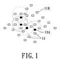
- FIG. 1is a schematic view of categorization of data points by using DBSCAN according to the present invention.
- FIG. 2is a flow chart of a method of adjusting wafer production sequences according to the present invention.
- FIG. 3is a schematic view of a production process according to the present invention.
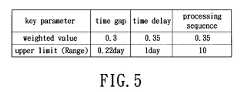
- FIG. 4shows key parameters for each lot according to the present invention.
- FIG. 5is a chart showing weight values and upper limits (Range) for the key parameters according to the present invention.
- FIG. 6shows the results of categorizing the lot NO. 01 according to the present invention.
- a method of adjusting the wafer processing sequencecategorizes lots according to their process recipe so that the lots with similar or the same process recipe are put in the same group.
- the original processing sequences of the categorized wafersare changed in a manner so that the same group of wafers is continuously or simultaneously processed in the same machine.
- the present inventionuses the clustering algorithm, density-based spatial clustering of application with noise (DBSCAN), to categorize a plurality of wafers into groups.
- DBSCANdensity-based spatial clustering of application with noise
- DBSCANselects those data points 11 which are closer to one another and put them into one group.
- two parametersneed to be set: an epsilon value and a minimum point number.
- a first steprandomly selects one of the data points as a starting point.
- the data point 11 Acan be the starting point.
- the difference between the starting point 11 a and other data points 11is calculated.
- the number of data points which have a difference smaller than the epsilon value from the starting point 11 Ais calculated; in other words, determine how many data points 11 are near the starting point 11 A to within the epsilon value. If the calculated number is larger than the minimum point number, then those data points 11 which have difference smaller than the epsilon value from the starting point 11 A, along with the starting point 11 A, are put into a group.
- a data point 11 Bis selected as a starting point, then because the number of the data points 11 that have difference smaller than the epsilon value from the starting point 11 B is less than the minimum point number, therefore the data point 11 B is marked as a noise.
- DBSCANcontinues to select other data points as a next starting point and repeats the above procedure to determine if the next starting point is to group with other data points close to it and form a group, or if the next starting point is a noise.
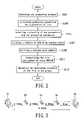
- FIG. 2shows the flow chart of implementation of the process according to the present invention.
- a processing procedureuses 4 machines, including a chemical vapor deposition (CVD) machine 22 , a wet etching machine 23 , an etchant cleaner 24 , and a photolithography machine 25 .
- CVDchemical vapor deposition
- a wet etching machine 23a wet etching machine 23 , an etchant cleaner 24 , and a photolithography machine 25 .
- One lotis subject to the sequential processing of the CVD machine 22 , the wet etching machine 23 , the etchant cleaner 24 , and the photolithography machine 25 after being processed in the machine 21 .
- the CVD machine 22 , the wet etching machine 23 , the etchant cleaner 24are referred to as reference machines, while the photolithography machine 25 is referred to as a target machine.
- all lotsare judged whether they have the same or similar process recipes according to their production parameters such as product specification and processing procedure. Those lots which have the same process recipe are adjusted so that they have the same processing sequence and thus are sent into the target machine.
- this target machinecan be a batch-type machine such as a furnace tool.
- step S 103collect all production parameters which are respectively obtained when the wafers are processed in the CVD machine 22 , the wet etching machine 23 , and the etchant cleaner 24 . Since the obtained production parameters are various, some key parameters need to be picked from them (Step S 105 ).
- a time gapis the period of time during which one lot is moved from the machine 21 to the photolithography machine 25 .
- the time delayis the period of time when one lot waits for entering the machine 21 .
- the processing sequenceis a sequence of determining which lot is processed earlier than others.
- FIG. 4shows the key parameters for each lot.
- the epsilon valueis obtained from the following formula (Step S 107 ):
- p iais an acceptable value for the key parameters
- p imis an upper limit within the range of the key parameters
- w iis a weighted value for each key parameter.
- the acceptable valuemeans if the difference (also referred to as “distinct” here below) between the production parameters for two lots is larger than the acceptable value, then the process recipes for those two lots are significantly different.
- the weighted valuegives the weight to one production parameter when compared to others.
- the upper limitis the maximum value for a production parameter.
- FIG. 5shows the corresponding weighted value, the upper limit, and the acceptable value for each production parameter, provided that the weighted sum of the three key production parameters equals to 1.
- iis set to 1-3.
- the epsilon valueis obtained to be 0.392912 from
- the upper limit (range) and the weighted valueare put into the formula.
- a minimum point numberis defined (Step S 109 ).
- the minimum point numberis 4, i.e., at least four lots are needed for forming a group.
- DBSCANis used to categorize those lots shown in FIG. 4 into a plurality of groups (Step S 111 ).
- one lotis randomly selected as a starting point.
- the lot NO. 01is used as the starting point.
- the production parameters of other lots NO. 02 to NO. 17are collected and their key parameters are selected respectively.
- Differences (“distinct”) between the key parameters of the starting point NO. 01 (lot NO. 01 ) and other points NO. 02 - 17 (lot NO. 02 - 17 )are subsequently obtained from the following formula:
- the difference (“distinct”) between the lot NO. 01 and the lot NO. 02is obtained from:
- FIG. 6shows the differences (“distinct”) of the starting point NO. 01 and other points NO. 02 - 17 .
- the numeral in the column of epsilon valueis 1, it means the difference between the calculated point and the starting point is smaller than the epsilon value.
- the numeral in the column of epsilon valueis 0, it means the difference between the calculated point and the starting point is larger than the epsilon value.
- the number of the lots which have differences smaller than the epsilon value from the starting pointi.e. the lot NO. 01
- the minimum point numberis 4, and the lots NO. 01 , 04 , 05 , 06 , 16 , and 17 are categorized into the same group.
- DBSCANselects another lot as a next starting point and repeats the above processing procedure.
- the processing sequenceis then adjusted so that those lots which have the same or similar process recipes are processed simultaneously or continuously (Step S 113 ). For example, when one group including the lots NO. 05 , 06 , and 16 is set to be processed later than the lots NO. 01 , NO. 04 , and NO. 17 , the processing sequences for the lots NO. 05 , NO. 06 , and NO. 16 are changed to be 1. In such situation, the lots in the same group can be sent continuously into the photolithography machine 25 in a manner such that the replacement of masks used for the photolithography machine 25 is reduced.
- the method of adjusting the wafer processing sequence according to the present inventionoffers the following advantages.
- DBSCANcategorizes a plurality of lots into groups so that lots with the same or similar process recipes are put into the same group.
- the processing sequences for the lots in the same groupare adjusted to be equal or almost equal so that they can be sent continuously or simultaneously into a machine. Thereby, the number of times for changing the process recipe for the same machine can be significantly reduced, or the idle time for the machine can be shortened.
- the key parametersare respectively given a weighted value so that the importance of the key parameters can be valued when the process sequence is to be adjusted. Therefore, the categorization of the lots by DBSCAN can be implemented with high precision.
Landscapes
- Engineering & Computer Science (AREA)
- General Engineering & Computer Science (AREA)
- Manufacturing & Machinery (AREA)
- Quality & Reliability (AREA)
- Physics & Mathematics (AREA)
- General Physics & Mathematics (AREA)
- Automation & Control Theory (AREA)
- Container, Conveyance, Adherence, Positioning, Of Wafer (AREA)
- General Factory Administration (AREA)
Abstract
Description
- 1. Field of the Invention
- The present invention relates to a method of adjusting the wafer processing sequence, and specially to a method of adjusting the wafer processing sequence for semiconductor manufacture.
- 2. Description of Related Art
- In semiconductor manufacturing, each lot of wafers (hereinafter referred as to “lot”) needs to be subjected to multiple processes through a plurality of machines. In favor of semiconductor producers' profit, reducing production time and increasing productivity are the endeavors the semiconductor producers have been pursuing.
- One of the key factors affecting the production time is the time for changing the process recipe. The machine needs to change its process recipe because of different designs of wafers. For example, the machine needs to adjust the processing parameters or replace modules for changing the process recipe. Therein, while the machine is changing the process recipe, the processing of wafers stops. Therefore, the longer the time needed for changing the process recipe, the longer it needs to finish the manufacturing of wafers. Some machines take less time to finish the change of process recipe. However, others, such as a photolithography machine, take much longer to do so.
- When the photolithography machine processes a first lot, it uses a first mask. Before proceeding the processing of a second lot with different process recipe, the first mask needs to be moved out and then a second mask need to be moved in. The replacement of the masks takes time; therefore the total production time for the second lot becomes longer.
- The other key factor is the time the machine waits for the next lot, even though the process recipes for the previous lot and the next lot are the same. Since the machine is a batch-type machine, the machine starts to operate only when a predetermined amount of lots with the same process recipe are inside the machine. For example, if the determined amount of lots is 4, the furnace tool starts to operate as soon as all four lots are inside the furnace tool. If the amount of lots has not reached the determined amount, then the machine does not work until the rest amount of lots has been supplied, which would lead to longer time for completing the manufacturing of wafers.
- In the view of above, if a process engineer fails to put those lots with the same recipe together when arranging the processing procedure, the time needed to finish the manufacture of wafers unavoidably increases.
- Therefore, there is a need for an improved method that overcomes the above disadvantages.
- It is one object of the present invention to provide a method of adjusting wafer processing sequence, which adjusts the processing sequence of lots of wafer (hereinafter referred as to “lots”) with the same recipe so that those lots can be processed continuously or simultaneously.
- In order to achieve the above objectives, the method of adjusting wafer process sequence of invention includes steps of: collecting production parameters for a plurality of lots; selecting a plurality of key parameters from the production parameters, wherein the key parameters at least includes a processing sequence; defining a formula to obtain an epsilon value, wherein the formula is
- piais an acceptable value, pimis an upper limit (Range) for the key parameters, and wiis a weighted value for the key parameters; defining a minimum point number; categorizing the lots into groups according to the epsilon value and the minimum point number by using density-based spatial clustering of application with noise (DBSCAN); and adjusting the processing sequences of the lots in the groups. The DBSCAN calculates the difference (“distinct” in the following formula) between production parameters (piand p′i) for two of the lots:
- The invention offers the following advantages.
- 1. DBSCAN is used to categorize a plurality of lots into groups so that lots with the same process recipes are put into the same group.
- 2. The processing sequences for the lots in the same group are adjusted to be equal or almost equal so that they can be sent continuously or simultaneously into a machine. Thereby, the number of times required for changing the process recipe for the same machine can be significantly reduced, or the idle time for the machine can be shortened.
- 3. The key parameters are respectively given a weighted value so that the importance of the key parameters can be valued when the process sequence is to be adjusted. Therefore, the categorization of the lots by DBSCAN can be implemented with high precision.
- In order to further understand the techniques, means, and effects the present invention takes for achieving the prescribed objectives, the following detailed descriptions and appended drawings are hereby referred; such that, through which the purposes, features, and aspects of the present invention can be thoroughly and concretely appreciated; however, the appended drawings are merely provided for reference and illustration, without any intention to be used for limiting the present invention.
FIG. 1 is a schematic view of categorization of data points by using DBSCAN according to the present invention.FIG. 2 is a flow chart of a method of adjusting wafer production sequences according to the present invention.FIG. 3 is a schematic view of a production process according to the present invention.FIG. 4 shows key parameters for each lot according to the present invention.FIG. 5 is a chart showing weight values and upper limits (Range) for the key parameters according to the present invention.FIG. 6 shows the results of categorizing the lot NO.01 according to the present invention.- In one of the preferred embodiments according to the present invention, a method of adjusting the wafer processing sequence categorizes lots according to their process recipe so that the lots with similar or the same process recipe are put in the same group. The original processing sequences of the categorized wafers are changed in a manner so that the same group of wafers is continuously or simultaneously processed in the same machine.
- In this embodiment, the present invention uses the clustering algorithm, density-based spatial clustering of application with noise (DBSCAN), to categorize a plurality of wafers into groups.
- Below is a brief description of DBSCAN. Referring to
FIG. 1 , if a plurality ofdata points 11 is arranged in a space, DBSCAN selects thosedata points 11 which are closer to one another and put them into one group. Before DBSCAN executes, two parameters need to be set: an epsilon value and a minimum point number. - When DBSCAN executes, a first step randomly selects one of the data points as a starting point. For example, the
data point 11A can be the starting point. Then the difference between the starting point11aandother data points 11 is calculated. The number of data points which have a difference smaller than the epsilon value from thestarting point 11A is calculated; in other words, determine howmany data points 11 are near thestarting point 11A to within the epsilon value. If the calculated number is larger than the minimum point number, then thosedata points 11 which have difference smaller than the epsilon value from thestarting point 11A, along with thestarting point 11A, are put into a group. On the other hand, if adata point 11B is selected as a starting point, then because the number of thedata points 11 that have difference smaller than the epsilon value from thestarting point 11B is less than the minimum point number, therefore thedata point 11B is marked as a noise. Similarly, DBSCAN continues to select other data points as a next starting point and repeats the above procedure to determine if the next starting point is to group with other data points close to it and form a group, or if the next starting point is a noise. FIG. 2 shows the flow chart of implementation of the process according to the present invention.- Referring to
FIG. 3 , in one of the preferred embodiment of the present invention, select a processing procedure (step S101). The processing procedure uses 4 machines, including a chemical vapor deposition (CVD)machine 22, awet etching machine 23, anetchant cleaner 24, and aphotolithography machine 25. One lot is subject to the sequential processing of theCVD machine 22, thewet etching machine 23, theetchant cleaner 24, and thephotolithography machine 25 after being processed in themachine 21. - The
CVD machine 22, thewet etching machine 23, theetchant cleaner 24 are referred to as reference machines, while thephotolithography machine 25 is referred to as a target machine. In the present invention, all lots are judged whether they have the same or similar process recipes according to their production parameters such as product specification and processing procedure. Those lots which have the same process recipe are adjusted so that they have the same processing sequence and thus are sent into the target machine. In other embodiments, this target machine can be a batch-type machine such as a furnace tool. - At the next step (step S103), collect all production parameters which are respectively obtained when the wafers are processed in the
CVD machine 22, thewet etching machine 23, and theetchant cleaner 24. Since the obtained production parameters are various, some key parameters need to be picked from them (Step S105). In the present embodiment, a time gap, a time delay, and a processing sequence are the key parameters. The time gap is the period of time during which one lot is moved from themachine 21 to thephotolithography machine 25. The time delay is the period of time when one lot waits for entering themachine 21. The processing sequence is a sequence of determining which lot is processed earlier than others.FIG. 4 shows the key parameters for each lot. - Below are the definitions of two parameters needed for DBSCAN: the epsilon value and the minimum point number. The epsilon value is obtained from the following formula (Step S107):
- wherein piais an acceptable value for the key parameters, pimis an upper limit within the range of the key parameters, and wiis a weighted value for each key parameter. The acceptable value means if the difference (also referred to as “distinct” here below) between the production parameters for two lots is larger than the acceptable value, then the process recipes for those two lots are significantly different. The weighted value gives the weight to one production parameter when compared to others. The upper limit is the maximum value for a production parameter.
FIG. 5 shows the corresponding weighted value, the upper limit, and the acceptable value for each production parameter, provided that the weighted sum of the three key production parameters equals to 1. - In the present embodiment which uses three key production parameter, i is set to 1-3. The epsilon value is obtained to be 0.392912 from
- , after the acceptable value, the upper limit (range) and the weighted value are put into the formula.
- Then, a minimum point number is defined (Step S109). In the present embodiment, the minimum point number is 4, i.e., at least four lots are needed for forming a group. Thereafter, DBSCAN is used to categorize those lots shown in
FIG. 4 into a plurality of groups (Step S111). - When DBSCAN starts to categorize, one lot is randomly selected as a starting point. For example, in the present embodiment, the lot NO.01 is used as the starting point. Then, the production parameters of other lots NO.02 to NO.17 are collected and their key parameters are selected respectively. Differences (“distinct”) between the key parameters of the starting point NO.01 (lot NO.01) and other points NO.02-17 (lot NO.02-17) are subsequently obtained from the following formula:
- , wherein pirepresents a key parameter for one lot, and p′imeans a key parameter for another lot. Taking the lot NO.02 as an example, the difference (“distinct”) between the lot NO.01 and the lot NO.02 is obtained from:
FIG. 6 shows the differences (“distinct”) of the starting point NO.01 and other points NO.02-17. When the numeral in the column of epsilon value is 1, it means the difference between the calculated point and the starting point is smaller than the epsilon value. On the other hand, when the numeral in the column of epsilon value is 0, it means the difference between the calculated point and the starting point is larger than the epsilon value.- At the next step, the number of the lots which have differences smaller than the epsilon value from the starting point (i.e. the lot NO.01) is calculated. In the present embodiment, there are in total 5 lots. Subsequently, determine whether this obtained number (i.e. 5) is larger than the minimum point number. If yes, then this means that those lots have difference smaller than the epsilon value, and so those lots along with the lot that acts as the starting point are categorized into one group; in other words, the 5 lots and the lot that acts as the starting point are categorized into one group. Specifically, in the present embodiment, the minimum point number is 4, and the lots NO.01,04,05,06,16, and17 are categorized into the same group. On the other hand, if the obtained number is smaller than the minimum point number, then DBSCAN selects another lot as a next starting point and repeats the above processing procedure.
- After DBSCAN categorizes those lots, the processing sequence is then adjusted so that those lots which have the same or similar process recipes are processed simultaneously or continuously (Step S113). For example, when one group including the lots NO.05,06, and16 is set to be processed later than the lots NO.01, NO.04, and NO.17, the processing sequences for the lots NO.05, NO.06, and NO.16 are changed to be 1. In such situation, the lots in the same group can be sent continuously into the
photolithography machine 25 in a manner such that the replacement of masks used for thephotolithography machine 25 is reduced. - In light of the above, the method of adjusting the wafer processing sequence according to the present invention offers the following advantages.
- 1. DBSCAN categorizes a plurality of lots into groups so that lots with the same or similar process recipes are put into the same group.
- 2. The processing sequences for the lots in the same group are adjusted to be equal or almost equal so that they can be sent continuously or simultaneously into a machine. Thereby, the number of times for changing the process recipe for the same machine can be significantly reduced, or the idle time for the machine can be shortened.
- 3. The key parameters are respectively given a weighted value so that the importance of the key parameters can be valued when the process sequence is to be adjusted. Therefore, the categorization of the lots by DBSCAN can be implemented with high precision.
- The above-mentioned descriptions represent merely the preferred embodiment of the present invention, without any intention to limit the scope of the present invention thereto. Various equivalent changes, alternations, or modifications based on the claims of present invention are all consequently viewed as being embraced by the scope of the present invention.
Claims (12)
Applications Claiming Priority (3)
| Application Number | Priority Date | Filing Date | Title |
|---|---|---|---|
| TW98111357 | 2009-04-06 | ||
| TW98111357A | 2009-04-06 | ||
| TW098111357ATWI388954B (en) | 2009-04-06 | 2009-04-06 | Method for adjusting priority of lot of wafer |
Publications (2)
| Publication Number | Publication Date |
|---|---|
| US20100256792A1true US20100256792A1 (en) | 2010-10-07 |
| US8244500B2 US8244500B2 (en) | 2012-08-14 |
Family
ID=42826877
Family Applications (1)
| Application Number | Title | Priority Date | Filing Date |
|---|---|---|---|
| US12/476,559Active2031-02-19US8244500B2 (en) | 2009-04-06 | 2009-06-02 | Method of adjusting wafer processing sequence |
Country Status (2)
| Country | Link |
|---|---|
| US (1) | US8244500B2 (en) |
| TW (1) | TWI388954B (en) |
Cited By (2)
| Publication number | Priority date | Publication date | Assignee | Title |
|---|---|---|---|---|
| CN103903276A (en)* | 2014-04-23 | 2014-07-02 | 吉林大学 | Driver fixation point clustering method based on density clustering method and morphology clustering method |
| CN104751261A (en)* | 2013-12-30 | 2015-07-01 | 中芯国际集成电路制造(上海)有限公司 | Technological process changing method and method for monitoring changed technological process |
Families Citing this family (3)
| Publication number | Priority date | Publication date | Assignee | Title |
|---|---|---|---|---|
| KR101794069B1 (en)* | 2010-05-26 | 2017-12-04 | 삼성전자주식회사 | equipment for manufacturing semiconductor device and seasoning process optimization method of the same |
| CN114037168B (en)* | 2021-11-16 | 2024-08-20 | 长江存储科技有限责任公司 | Method and device for improving production efficiency of machine and processing system |
| CN116579466B (en)* | 2023-04-25 | 2024-05-14 | 上海赛美特软件科技股份有限公司 | Reservation method and reservation device in wafer processing process |
Citations (9)
| Publication number | Priority date | Publication date | Assignee | Title |
|---|---|---|---|---|
| US5546312A (en)* | 1993-09-20 | 1996-08-13 | Texas Instruments Incorporated | Use of spatial models for simultaneous control of various non-uniformity metrics |
| US5991699A (en)* | 1995-05-04 | 1999-11-23 | Kla Instruments Corporation | Detecting groups of defects in semiconductor feature space |
| US6003029A (en)* | 1997-08-22 | 1999-12-14 | International Business Machines Corporation | Automatic subspace clustering of high dimensional data for data mining applications |
| US6961626B1 (en)* | 2004-05-28 | 2005-11-01 | Applied Materials, Inc | Dynamic offset and feedback threshold |
| US7221990B2 (en)* | 2004-05-28 | 2007-05-22 | Applied Materials, Inc. | Process control by distinguishing a white noise component of a process variance |
| US20070282475A1 (en)* | 2006-05-31 | 2007-12-06 | Kilian Schmidt | Method and system for determining utilization of process tools in a manufacturing environment based on characteristics of an automated material handling system |
| US20080027577A1 (en)* | 2004-07-12 | 2008-01-31 | Horak David V | Feature dimension deviation correction system, method and program product |
| US7340320B2 (en)* | 2005-04-13 | 2008-03-04 | Asm Japan K.K. | Method of recipe control operation |
| US20080306621A1 (en)* | 2007-06-05 | 2008-12-11 | Sang-Wook Choi | Semiconductor manufacturing apparatus control system and statistical process control method thereof |
- 2009
- 2009-04-06TWTW098111357Apatent/TWI388954B/enactive
- 2009-06-02USUS12/476,559patent/US8244500B2/enactiveActive
Patent Citations (9)
| Publication number | Priority date | Publication date | Assignee | Title |
|---|---|---|---|---|
| US5546312A (en)* | 1993-09-20 | 1996-08-13 | Texas Instruments Incorporated | Use of spatial models for simultaneous control of various non-uniformity metrics |
| US5991699A (en)* | 1995-05-04 | 1999-11-23 | Kla Instruments Corporation | Detecting groups of defects in semiconductor feature space |
| US6003029A (en)* | 1997-08-22 | 1999-12-14 | International Business Machines Corporation | Automatic subspace clustering of high dimensional data for data mining applications |
| US6961626B1 (en)* | 2004-05-28 | 2005-11-01 | Applied Materials, Inc | Dynamic offset and feedback threshold |
| US7221990B2 (en)* | 2004-05-28 | 2007-05-22 | Applied Materials, Inc. | Process control by distinguishing a white noise component of a process variance |
| US20080027577A1 (en)* | 2004-07-12 | 2008-01-31 | Horak David V | Feature dimension deviation correction system, method and program product |
| US7340320B2 (en)* | 2005-04-13 | 2008-03-04 | Asm Japan K.K. | Method of recipe control operation |
| US20070282475A1 (en)* | 2006-05-31 | 2007-12-06 | Kilian Schmidt | Method and system for determining utilization of process tools in a manufacturing environment based on characteristics of an automated material handling system |
| US20080306621A1 (en)* | 2007-06-05 | 2008-12-11 | Sang-Wook Choi | Semiconductor manufacturing apparatus control system and statistical process control method thereof |
Non-Patent Citations (2)
| Title |
|---|
| A Density-Based Algorithm for Discovering Clusters in Large Spatial Databases With Noise, Ester et al., 1996* |
| Error-Aware Density-Based Clustering of Imprecise Measurement Values, Habich et al., IEEE 2007.* |
Cited By (2)
| Publication number | Priority date | Publication date | Assignee | Title |
|---|---|---|---|---|
| CN104751261A (en)* | 2013-12-30 | 2015-07-01 | 中芯国际集成电路制造(上海)有限公司 | Technological process changing method and method for monitoring changed technological process |
| CN103903276A (en)* | 2014-04-23 | 2014-07-02 | 吉林大学 | Driver fixation point clustering method based on density clustering method and morphology clustering method |
Also Published As
| Publication number | Publication date |
|---|---|
| US8244500B2 (en) | 2012-08-14 |
| TWI388954B (en) | 2013-03-11 |
| TW201037472A (en) | 2010-10-16 |
Similar Documents
| Publication | Publication Date | Title |
|---|---|---|
| US8244500B2 (en) | Method of adjusting wafer processing sequence | |
| US9513565B2 (en) | Using wafer geometry to improve scanner correction effectiveness for overlay control | |
| US8683395B2 (en) | Method and system for feed-forward advanced process control | |
| TWI509551B (en) | System and method for manufacturing semiconductor | |
| CN112534561B (en) | Compensate for chamber and process effects to improve critical dimension variations in trim processes | |
| US20110238198A1 (en) | Method and system for implementing virtual metrology in semiconductor fabrication | |
| CN102063063B (en) | Semiconductor manufacturing method and system | |
| US8406912B2 (en) | System and method for data mining and feature tracking for fab-wide prediction and control | |
| CN101493655B (en) | Exposure method | |
| US10522427B2 (en) | Techniques providing semiconductor wafer grouping in a feed forward process | |
| US7130762B2 (en) | Method and system for handling substrates in a production line including a cluster tool and a metrology tool | |
| US8489218B2 (en) | Chamber match using important variables filtered by dynamic multivariate analysis | |
| US7767471B2 (en) | Auto routing for optimal uniformity control | |
| US8394719B2 (en) | System and method for implementing multi-resolution advanced process control | |
| US20160274570A1 (en) | Method of virtual metrology using combined models | |
| JP2006173373A (en) | Manufacturing system of semiconductor product | |
| Sarfaty et al. | Advance process control solutions for semiconductor manufacturing | |
| US7502658B1 (en) | Methods of fabricating optimization involving process sequence analysis | |
| US8239151B2 (en) | Method and apparatus for analysis of continuous data using binary parsing | |
| JP2009170502A (en) | Supporting system for semiconductor manufacturing | |
| US20090125140A1 (en) | System and method for matching silicon oxide thickness between similar process tools | |
| US7738986B2 (en) | Method and apparatus for compensating metrology data for site bias prior to filtering | |
| US7236840B2 (en) | Manufacturing process developing method for semiconductor device | |
| US6865438B1 (en) | Method of using time interval in IC foundry to control feed back system | |
| US8219341B2 (en) | System and method for implementing wafer acceptance test (“WAT”) advanced process control (“APC”) with routing model |
Legal Events
| Date | Code | Title | Description |
|---|---|---|---|
| AS | Assignment | Owner name:INOTERA MEMORIES, INC., TAIWAN Free format text:ASSIGNMENT OF ASSIGNORS INTEREST;ASSIGNORS:TIAN, YUN-ZONG;CHEN, CHUN CHI;LEE, YI FENG;AND OTHERS;REEL/FRAME:022840/0635 Effective date:20090602 | |
| STCF | Information on status: patent grant | Free format text:PATENTED CASE | |
| FEPP | Fee payment procedure | Free format text:PAT HOLDER NO LONGER CLAIMS SMALL ENTITY STATUS, ENTITY STATUS SET TO UNDISCOUNTED (ORIGINAL EVENT CODE: STOL); ENTITY STATUS OF PATENT OWNER: LARGE ENTITY Free format text:PAT HOLDER CLAIMS SMALL ENTITY STATUS, ENTITY STATUS SET TO SMALL (ORIGINAL EVENT CODE: LTOS); ENTITY STATUS OF PATENT OWNER: LARGE ENTITY | |
| FPAY | Fee payment | Year of fee payment:4 | |
| AS | Assignment | Owner name:MORGAN STANLEY SENIOR FUNDING, INC., MARYLAND Free format text:SUPPLEMENT NO. 3 TO PATENT SECURITY AGREEMENT;ASSIGNOR:MICRON TECHNOLOGY, INC.;REEL/FRAME:041675/0105 Effective date:20170124 | |
| AS | Assignment | Owner name:MICRON TECHNOLOGY, INC., IDAHO Free format text:ASSIGNMENT OF ASSIGNORS INTEREST;ASSIGNOR:INOTERA MEMORIES, INC.;REEL/FRAME:041820/0815 Effective date:20170222 | |
| FEPP | Fee payment procedure | Free format text:PAYOR NUMBER ASSIGNED (ORIGINAL EVENT CODE: ASPN) | |
| AS | Assignment | Owner name:JPMORGAN CHASE BANK, N.A., AS COLLATERAL AGENT, ILLINOIS Free format text:SECURITY INTEREST;ASSIGNORS:MICRON TECHNOLOGY, INC.;MICRON SEMICONDUCTOR PRODUCTS, INC.;REEL/FRAME:047540/0001 Effective date:20180703 Owner name:JPMORGAN CHASE BANK, N.A., AS COLLATERAL AGENT, IL Free format text:SECURITY INTEREST;ASSIGNORS:MICRON TECHNOLOGY, INC.;MICRON SEMICONDUCTOR PRODUCTS, INC.;REEL/FRAME:047540/0001 Effective date:20180703 | |
| AS | Assignment | Owner name:MICRON TECHNOLOGY, INC., IDAHO Free format text:RELEASE BY SECURED PARTY;ASSIGNOR:MORGAN STANLEY SENIOR FUNDING, INC., AS COLLATERAL AGENT;REEL/FRAME:050695/0825 Effective date:20190731 | |
| AS | Assignment | Owner name:MICRON SEMICONDUCTOR PRODUCTS, INC., IDAHO Free format text:RELEASE BY SECURED PARTY;ASSIGNOR:JPMORGAN CHASE BANK, N.A., AS COLLATERAL AGENT;REEL/FRAME:051028/0001 Effective date:20190731 Owner name:MICRON TECHNOLOGY, INC., IDAHO Free format text:RELEASE BY SECURED PARTY;ASSIGNOR:JPMORGAN CHASE BANK, N.A., AS COLLATERAL AGENT;REEL/FRAME:051028/0001 Effective date:20190731 | |
| MAFP | Maintenance fee payment | Free format text:PAYMENT OF MAINTENANCE FEE, 8TH YEAR, LARGE ENTITY (ORIGINAL EVENT CODE: M1552); ENTITY STATUS OF PATENT OWNER: LARGE ENTITY Year of fee payment:8 | |
| MAFP | Maintenance fee payment | Free format text:PAYMENT OF MAINTENANCE FEE, 12TH YEAR, LARGE ENTITY (ORIGINAL EVENT CODE: M1553); ENTITY STATUS OF PATENT OWNER: LARGE ENTITY Year of fee payment:12 |