US20100255630A1 - Sodium-incorporation in solar cell substrates and contacts - Google Patents
Sodium-incorporation in solar cell substrates and contactsDownload PDFInfo
- Publication number
- US20100255630A1 US20100255630A1US12/820,560US82056010AUS2010255630A1US 20100255630 A1US20100255630 A1US 20100255630A1US 82056010 AUS82056010 AUS 82056010AUS 2010255630 A1US2010255630 A1US 2010255630A1
- Authority
- US
- United States
- Prior art keywords
- substrate
- sodium
- front surface
- back contact
- thin
- Prior art date
- Legal status (The legal status is an assumption and is not a legal conclusion. Google has not performed a legal analysis and makes no representation as to the accuracy of the status listed.)
- Granted
Links
Images


Classifications
- E—FIXED CONSTRUCTIONS
- E06—DOORS, WINDOWS, SHUTTERS, OR ROLLER BLINDS IN GENERAL; LADDERS
- E06B—FIXED OR MOVABLE CLOSURES FOR OPENINGS IN BUILDINGS, VEHICLES, FENCES OR LIKE ENCLOSURES IN GENERAL, e.g. DOORS, WINDOWS, BLINDS, GATES
- E06B7/00—Special arrangements or measures in connection with doors or windows
- E06B7/02—Special arrangements or measures in connection with doors or windows for providing ventilation, e.g. through double windows; Arrangement of ventilation roses
- E06B7/08—Louvre doors, windows or grilles
- B—PERFORMING OPERATIONS; TRANSPORTING
- B32—LAYERED PRODUCTS
- B32B—LAYERED PRODUCTS, i.e. PRODUCTS BUILT-UP OF STRATA OF FLAT OR NON-FLAT, e.g. CELLULAR OR HONEYCOMB, FORM
- B32B37/00—Methods or apparatus for laminating, e.g. by curing or by ultrasonic bonding
- B32B37/02—Methods or apparatus for laminating, e.g. by curing or by ultrasonic bonding characterised by a sequence of laminating steps, e.g. by adding new layers at consecutive laminating stations
- H—ELECTRICITY
- H10—SEMICONDUCTOR DEVICES; ELECTRIC SOLID-STATE DEVICES NOT OTHERWISE PROVIDED FOR
- H10F—INORGANIC SEMICONDUCTOR DEVICES SENSITIVE TO INFRARED RADIATION, LIGHT, ELECTROMAGNETIC RADIATION OF SHORTER WAVELENGTH OR CORPUSCULAR RADIATION
- H10F77/00—Constructional details of devices covered by this subclass
- H10F77/10—Semiconductor bodies
- H10F77/16—Material structures, e.g. crystalline structures, film structures or crystal plane orientations
- H10F77/169—Thin semiconductor films on metallic or insulating substrates
- H10F77/1694—Thin semiconductor films on metallic or insulating substrates the films including Group I-III-VI materials, e.g. CIS or CIGS
- H—ELECTRICITY
- H10—SEMICONDUCTOR DEVICES; ELECTRIC SOLID-STATE DEVICES NOT OTHERWISE PROVIDED FOR
- H10F—INORGANIC SEMICONDUCTOR DEVICES SENSITIVE TO INFRARED RADIATION, LIGHT, ELECTROMAGNETIC RADIATION OF SHORTER WAVELENGTH OR CORPUSCULAR RADIATION
- H10F77/00—Constructional details of devices covered by this subclass
- H10F77/10—Semiconductor bodies
- H10F77/16—Material structures, e.g. crystalline structures, film structures or crystal plane orientations
- H10F77/169—Thin semiconductor films on metallic or insulating substrates
- H10F77/1696—Thin semiconductor films on metallic or insulating substrates the films including Group II-VI materials, e.g. CdTe or CdS
- H—ELECTRICITY
- H10—SEMICONDUCTOR DEVICES; ELECTRIC SOLID-STATE DEVICES NOT OTHERWISE PROVIDED FOR
- H10F—INORGANIC SEMICONDUCTOR DEVICES SENSITIVE TO INFRARED RADIATION, LIGHT, ELECTROMAGNETIC RADIATION OF SHORTER WAVELENGTH OR CORPUSCULAR RADIATION
- H10F77/00—Constructional details of devices covered by this subclass
- H10F77/10—Semiconductor bodies
- H10F77/16—Material structures, e.g. crystalline structures, film structures or crystal plane orientations
- H10F77/169—Thin semiconductor films on metallic or insulating substrates
- H10F77/1698—Thin semiconductor films on metallic or insulating substrates the metallic or insulating substrates being flexible
- H10F77/1699—Thin semiconductor films on metallic or insulating substrates the metallic or insulating substrates being flexible the films including Group I-III-VI materials, e.g. CIS or CIGS on metal foils or polymer foils
- B—PERFORMING OPERATIONS; TRANSPORTING
- B32—LAYERED PRODUCTS
- B32B—LAYERED PRODUCTS, i.e. PRODUCTS BUILT-UP OF STRATA OF FLAT OR NON-FLAT, e.g. CELLULAR OR HONEYCOMB, FORM
- B32B2310/00—Treatment by energy or chemical effects
- B32B2310/08—Treatment by energy or chemical effects by wave energy or particle radiation
- B32B2310/0806—Treatment by energy or chemical effects by wave energy or particle radiation using electromagnetic radiation
- B32B2310/0843—Treatment by energy or chemical effects by wave energy or particle radiation using electromagnetic radiation using laser
- B—PERFORMING OPERATIONS; TRANSPORTING
- B32—LAYERED PRODUCTS
- B32B—LAYERED PRODUCTS, i.e. PRODUCTS BUILT-UP OF STRATA OF FLAT OR NON-FLAT, e.g. CELLULAR OR HONEYCOMB, FORM
- B32B2311/00—Metals, their alloys or their compounds
- B—PERFORMING OPERATIONS; TRANSPORTING
- B32—LAYERED PRODUCTS
- B32B—LAYERED PRODUCTS, i.e. PRODUCTS BUILT-UP OF STRATA OF FLAT OR NON-FLAT, e.g. CELLULAR OR HONEYCOMB, FORM
- B32B2311/00—Metals, their alloys or their compounds
- B32B2311/24—Aluminium
- B—PERFORMING OPERATIONS; TRANSPORTING
- B32—LAYERED PRODUCTS
- B32B—LAYERED PRODUCTS, i.e. PRODUCTS BUILT-UP OF STRATA OF FLAT OR NON-FLAT, e.g. CELLULAR OR HONEYCOMB, FORM
- B32B2367/00—Polyesters, e.g. PET, i.e. polyethylene terephthalate
- B—PERFORMING OPERATIONS; TRANSPORTING
- B32—LAYERED PRODUCTS
- B32B—LAYERED PRODUCTS, i.e. PRODUCTS BUILT-UP OF STRATA OF FLAT OR NON-FLAT, e.g. CELLULAR OR HONEYCOMB, FORM
- B32B2457/00—Electrical equipment
- B32B2457/12—Photovoltaic modules
- B—PERFORMING OPERATIONS; TRANSPORTING
- B32—LAYERED PRODUCTS
- B32B—LAYERED PRODUCTS, i.e. PRODUCTS BUILT-UP OF STRATA OF FLAT OR NON-FLAT, e.g. CELLULAR OR HONEYCOMB, FORM
- B32B37/00—Methods or apparatus for laminating, e.g. by curing or by ultrasonic bonding
- B32B37/12—Methods or apparatus for laminating, e.g. by curing or by ultrasonic bonding characterised by using adhesives
- B—PERFORMING OPERATIONS; TRANSPORTING
- B32—LAYERED PRODUCTS
- B32B—LAYERED PRODUCTS, i.e. PRODUCTS BUILT-UP OF STRATA OF FLAT OR NON-FLAT, e.g. CELLULAR OR HONEYCOMB, FORM
- B32B38/00—Ancillary operations in connection with laminating processes
- B32B38/0004—Cutting, tearing or severing, e.g. bursting; Cutter details
- B—PERFORMING OPERATIONS; TRANSPORTING
- B32—LAYERED PRODUCTS
- B32B—LAYERED PRODUCTS, i.e. PRODUCTS BUILT-UP OF STRATA OF FLAT OR NON-FLAT, e.g. CELLULAR OR HONEYCOMB, FORM
- B32B38/00—Ancillary operations in connection with laminating processes
- B32B38/06—Embossing
- H—ELECTRICITY
- H10—SEMICONDUCTOR DEVICES; ELECTRIC SOLID-STATE DEVICES NOT OTHERWISE PROVIDED FOR
- H10F—INORGANIC SEMICONDUCTOR DEVICES SENSITIVE TO INFRARED RADIATION, LIGHT, ELECTROMAGNETIC RADIATION OF SHORTER WAVELENGTH OR CORPUSCULAR RADIATION
- H10F71/00—Manufacture or treatment of devices covered by this subclass
- H10F71/10—Manufacture or treatment of devices covered by this subclass the devices comprising amorphous semiconductor material
- H10F71/107—Continuous treatment of the devices, e.g. roll-to roll processes or multi-chamber deposition
- H—ELECTRICITY
- H10—SEMICONDUCTOR DEVICES; ELECTRIC SOLID-STATE DEVICES NOT OTHERWISE PROVIDED FOR
- H10F—INORGANIC SEMICONDUCTOR DEVICES SENSITIVE TO INFRARED RADIATION, LIGHT, ELECTROMAGNETIC RADIATION OF SHORTER WAVELENGTH OR CORPUSCULAR RADIATION
- H10F77/00—Constructional details of devices covered by this subclass
- H10F77/10—Semiconductor bodies
- H10F77/12—Active materials
- H10F77/126—Active materials comprising only Group I-III-VI chalcopyrite materials, e.g. CuInSe2, CuGaSe2 or CuInGaSe2 [CIGS]
- Y—GENERAL TAGGING OF NEW TECHNOLOGICAL DEVELOPMENTS; GENERAL TAGGING OF CROSS-SECTIONAL TECHNOLOGIES SPANNING OVER SEVERAL SECTIONS OF THE IPC; TECHNICAL SUBJECTS COVERED BY FORMER USPC CROSS-REFERENCE ART COLLECTIONS [XRACs] AND DIGESTS
- Y02—TECHNOLOGIES OR APPLICATIONS FOR MITIGATION OR ADAPTATION AGAINST CLIMATE CHANGE
- Y02E—REDUCTION OF GREENHOUSE GAS [GHG] EMISSIONS, RELATED TO ENERGY GENERATION, TRANSMISSION OR DISTRIBUTION
- Y02E10/00—Energy generation through renewable energy sources
- Y02E10/50—Photovoltaic [PV] energy
- Y02E10/541—CuInSe2 material PV cells
- Y—GENERAL TAGGING OF NEW TECHNOLOGICAL DEVELOPMENTS; GENERAL TAGGING OF CROSS-SECTIONAL TECHNOLOGIES SPANNING OVER SEVERAL SECTIONS OF THE IPC; TECHNICAL SUBJECTS COVERED BY FORMER USPC CROSS-REFERENCE ART COLLECTIONS [XRACs] AND DIGESTS
- Y02—TECHNOLOGIES OR APPLICATIONS FOR MITIGATION OR ADAPTATION AGAINST CLIMATE CHANGE
- Y02P—CLIMATE CHANGE MITIGATION TECHNOLOGIES IN THE PRODUCTION OR PROCESSING OF GOODS
- Y02P70/00—Climate change mitigation technologies in the production process for final industrial or consumer products
- Y02P70/50—Manufacturing or production processes characterised by the final manufactured product
Definitions
- Solar cellsare widely used to collect solar energy and generate electricity, with multiple solar cells interconnected to form solar panels.
- solar collectorsThere are two main types of solar collectors: silicon and thin-film solar collectors.
- Siliconis currently the predominant technology, using silicon-based cells encapsulated behind glass.
- Thin-film processesinvolve depositing thin-film materials on a substrate to form a light absorbing layer sandwiched between electrical contact layers.
- the front or top contactis a transparent and conductive layer for current collection and light enhancement
- the light absorbing layeris a semiconductor material
- the back contactis a conductive layer to provide electrical current throughout the cell.
- a metallic back electrical contact layeris deposited on a substrate.
- a p-type semiconductor layeris then deposited on the back electrical contact layer and an n-type semiconductor layer is deposited on the p-type semiconductor layer to complete a p-n junction.
- Any suitable semiconductor materialssuch as CIGS, CIS, CdTe, CdS, ZnS, ZnO, amorphous silicon, polycrystalline silicon, etc. may be used for these layers.
- a top transparent electrode layeris then deposited on the p-n junction. This layer may be a conductive oxide or other conductive film and is used for current collection. Once these or other materials have been deposited on the substrate to form a photovoltaic stack, the substrate and thin-film materials deposited may be cut into cells. Multiple cells are then assembled into a thin-film solar panel.
- Thin-film solar collectorsare lower cost and require lower energy to produce.
- there are numerous sources of defects in a thin-film panelgiven the materials used, the large surfaces areas required, the small thicknesses of films, and the sensitivity of the films to small particles.
- a one micron particleis on the order of the film thickness. Defects from particles and other sources can cause shunts and otherwise compromise solar cell performance.
- sodiumis incorporated into a substrate or a back contact of a thin-film photovoltaic stack where it can diffuse into a CIGS or other absorber layer to improve efficiency and/or growth of the layer.
- the methodsinvolve laser treating the substrate or back contact in the presence of a sodium (or sodium-containing) solid or vapor to thereby incorporate sodium into the surface of the substrate or back contact.
- the surfaceis simultaneously smoothed.
- One aspect of the inventionrelates to a method of incorporating sodium into a substrate of a thin-film photovoltaic stack, involving providing a substrate for thin-film photovoltaic stack; treating a front surface of the substrate with sodium; and irradiating the front surface with a plurality of laser beams at a plurality of spots on the substrate surface to thereby form molten mixtures of a substrate material and sodium; and solidifying the molten mixtures.
- the substrateis a metal substrate, e.g., a stainless steel foil. Treating the front surface of the substrate may involve any of depositing solid sodium (Na) on the front surface, depositing a solid sodium-containing compound such as NaF, NaCl, NaS, NaOH or any other compound on the front surface, precipitating a sodium-containing liquid on the surface, coating the surface with a sodium-containing solution or exposing the front surface to a sodium-containing vapor while irradiating the front surface with the plurality of laser beams.
- sodiumis incorporated in the substrate such that there is a concentration gradient of sodium across a substrate thickness having a maximum at the front surface.
- Another aspect of the inventioninvolves incorporating sodium into a back contact of a thin-film photovoltaic stack, involving providing a substrate for thin-film photovoltaic stack, said substrate having a thin-film back contact deposited thereon; treating a front surface of the back contact with sodium; irradiating the front surface with a plurality of laser beams at a plurality of spots on the back contact surface to thereby form molten mixtures of a back contact material and sodium; and solidifying the molten mixtures.
- the back contactis a molybdenum thin-film.
- Treating the front surface of the back contactmay involve any of depositing solid sodium (Na) on the front surface, depositing a solid sodium-containing compound such as NaF, NaCl, NaS, NaOH or any other compound on the front surface, precipitating a sodium-containing liquid on the surface, coating the surface with a sodium-containing solution or exposing the front surface to a sodium-containing vapor while irradiating the front surface with the plurality of laser beams.
- sodiumis incorporated in the back contact such that there is a concentration gradient of sodium across a back contact thickness having a maximum at the front surface.
- Another aspect of the inventionrelates to incorporating an additive into a substrate or back contact layer of a thin-film photovoltaic stack, involving providing a partially fabricated thin-film photovoltaic stack, said partially fabricated thin-film photovoltaic stack including at least a substrate; treating a front surface of the partially fabricated thin-film photovoltaic stack with an additive; irradiating the front surface with a plurality of laser beams at a plurality of spots on the substrate surface to thereby form molten mixtures of a substrate or back contact material and the additive; and solidifying the molten mixtures.
- FIG. 1depicts schematic illustrations of a thin-film solar cell and two monolithically integrated thin-film solar cells according to certain embodiments.
- FIG. 2Adepicts a schematic illustration of laser polishing of a substrate of a thin-film photovoltaic stack according to certain embodiments.
- FIG. 2Bdepicts a schematic illustration of laser polishing of a back contact of a thin-film photovoltaic stack according to certain embodiments.
- FIG. 2Cdepicts a schematic illustration of laser cleaning of a surface of a layer in a thin-film photovoltaic stack according to certain embodiments.
- FIG. 3is a simplified diagram showing a deposition apparatus for depositing thin film photovoltaic materials on a web substrate including a laser polishing apparatus according to certain embodiments.
- FIG. 4depicts schematic illustrations of examples of high frequency roughness, low frequency roughness (waviness) and flatness scales of thin-film photovoltaic stacks according to certain embodiments.
- FIG. 5depicts top and side views of an overlapping texture pattern according to certain embodiments.
- FIG. 6is an image showing an example of a laser textured feature formed in a nickel surface.
- FIG. 7Ashows two images of surface finishes of 300 series stainless steel surface prior to laser treatment.
- FIG. 7Bshows an image of a surface finish of a 300 series stainless steel surface after laser treatment according to certain embodiments.
- FIG. 8shows two examples of texturing a surface of substrate in an ellipsoidal pattern according to certain embodiments.
- FIG. 9is a process flow diagram illustrating operations in a method of laser polishing or texturing a back contact film of a thin-film photovoltaic stack according to certain embodiments.
- FIGS. 10 and 11are process flow diagrams illustrating operations in methods of incorporating sodium into a thin-film photovoltaic stack according to certain embodiments.
- FIGS. 12A and 12Bdepict components of a laser polishing apparatus according to certain embodiments.
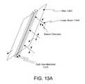
- FIGS. 13A and 13Bdepict components of a laser treatment apparatus according to certain embodiments.
- Thin-film solar panelshave many advantages, including providing low cost, low energy production. However, there are numerous sources of defects in a thin-film panel, given materials used, the large surfaces areas required, the small thicknesses of films, and the sensitivity of the films to small particles. For example, a one micron particle is on the order of the film thickness. Defects from particles and other causes can cause shunts and otherwise compromise solar cell performance.
- substrate preparationAnother factor related to defects is the level of substrate preparation.
- substrate (semiconductor wafer) preparationinvolves chemical-mechanical planarization and cleaning prior to wafers being released into the line.
- media productionnear sub-single nanometer polish levels are achieved.
- these techniquesare highly complex and expensive in comparison to what can reasonably be done as pre-preparation prior to film deposition for a large area solar panel.
- Any large area, economical method of substrate preparationis likely to leave some level of high-frequency roughness, in comparison to the film thickness.
- any robust and high yielding thin-film solar producthas a certain number of defects accounted for in the product and process design.
- wafer flatness requirements for photolithography, probing and other concerns, and magnetic media for spacing controlthere are no significant waviness or flatness requirements for large area photovoltaic panels.
- Shunt sitesmay be present on fabrication or can develop during the lifetime of a solar panel. This development can be related to moisture ingress, collection of ionic contaminants, changes in stress/strain in the film or package or thermal cycling. A new site near a collection line can sink nearly all current generated in a typical cell, and can actually melt the encapsulating material, allowing for additional environmental degradation.
- the use of serialized cell strings where the voltages are increased across an individual cellplace even greater stresses on defect sites and film continuity, the opportunity for field damage to occur in a shaded or poor performing cell.
- other problematic results of film defectsinclude low film performance due to poor junction formation and film delamination.
- Laser polishingrefers to smoothing a surface of a substrate or back contact layer by exposing one or more localized areas or sites of the surface to laser irradiation, thereby creating a melt pool centered on the site of irradiation, and allowing the melted surface material to re-solidify.
- high frequency surface roughnessis removed.
- surface wavinessis removed.
- Laser texturing as described hereinrefers to a process of exposing a surface of a substrate or back contact layer to laser irradiation to create a surface pattern having long range order.
- Long range orderrefers to a substantially uniform pattern over a surface area of at least tens of square feet.
- laser texturinginvolves forming an interconnected low frequency patterned surface, the pattern surface frequency being between about 5 and 200 microns.
- the surfaceis provided having textured features from a rolling or other process. Such a surface may be retextured using laser irradiation.
- a laser textured surfacemay be characterized by one or more of: overlapping features, a substantially uniform array of features having a center-to-center distance of between about 5 and 200 microns, a substantially uniform array of features having circular symmetry, a substantially uniform array of features having non-circular symmetry, or a substantially uniform array of features having a center-to-center distance less than the natural length scale of the features.
- Laser texturingmay involve rastering a laser beam in a first direction, while moving the surface in a second direction, such that features are formed across a surface at a 100-1000 kHz repetition rate.
- Laser cleaning as described hereinrefers to a process of removing organic or inorganic contamination from a surface of a substrate or back contact.
- the contaminationmay be in the form of discrete particles or may be in the form of smeared material.
- the methodsinvolve removing defects from a material surface by rapidly heating the surface in an area of about 5-200 microns to form shallow (about 10-1000 angstroms deep) and rapidly expanding melt pools, followed by rapid cooling of the surface.
- the minimization of surface tensioncauses the surface to re-solidify in a locally smooth surface. That is, high frequency roughness is smoothed out, with a lower frequency bump or texture pattern remaining in certain embodiments after resolidification. Cooling of the surface may be active or passive according to various embodiments.
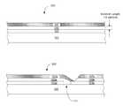
- FIG. 1includes a not-too-scale schematic of a thin-film photovoltaic stack 100 of a photovoltaic cell.
- Substrate 101supports thin-film layers 103 , 105 and 107 .
- thickness of the substrate 101may be on the order of mils, the thickness of the thin-film stack on the order of microns (or hundredths of mils).
- Substrate 101may be a metallic or polymeric material.
- the substrate 101is relatively thin, such as for example, between about 2-100 mils, or in certain embodiments, 2-10 mils. However, other suitable thicknesses may also be used, e.g., 50 mils.
- Back electrical contact layer 103provides electrical contact to allow electrical current to flow through the photovoltaic cell, and may be made of any appropriate material, e.g., molybdenum, niobium, copper, silver, etc.
- Layer 107is a top transparent electrode layer. In certain embodiments, it is a transparent conducting oxide (TCO), for example, zinc oxide, aluminum-doped zinc oxide and indium tin oxide.
- TCOtransparent conducting oxide
- Layer 105represents several thin-films deposited between back electrical contact layer 103 and top transparent electrical contact layer 107 , including a p-n junction. To form the p-n junction, a p-type semiconductor layer is deposited on back electrical contact layer 103 and an n-type semiconductor layer is deposited on the p-type semiconductor layer.
- any suitable semiconductor materialssuch as CIGS, CIS, CdTe, CdS, ZnS, ZnO, amorphous silicon, polycrystalline silicon, etc. are used to form the p-n junction.
- the p-type semiconductor layermay be CIGS or CIS
- the n-type semiconductor layermay be CdS or a cadmium free material, such as ZnS, ZnO, etc.
- Embodiments of the inventionare not limited to these p-n junctions, but include any appropriate p-n junction produced either as a homojunction in a single semiconductor material, or alternatively as a heterojunction between two different semiconductor materials.
- other thin-film layersmay be deposited between the electrical contact layers 103 and 107 .
- electrical contact layers 103 and 107are separated by a distance of about 1-2 microns. Any ionic contamination and moisture, cutting defects (for non-monolithically integrated cells), conductive contamination, or film delamination can lead to shunting sites, resulting in manufacturing or latent defects. In particular, the presence of any defect in the substrate may cause shunting at the time of deposition, or make the stack susceptible to developing shunts.
- FIG. 1also depicts a not-to-scale schematic illustration of two monolithically integrated stacks at 102 .
- a first stack including thin-film layers 103 a , 105 a and 107 ais electrically connected to a second stack including thin-film layers 103 b , 105 b and 107 b at a site 111 , with top contact layer 107 a and back contact 103 b separated into interconnected sections.
- the site 111 of film discontinuitiesis a likely point of moisture ingress, which can lead to shunting.
- photovoltaic thin-film stacks depicted in FIG. 1are deposited on a section of a substrate 101 after it has been polished, and contains no substantial defects, particles, or areas of high roughness. As such no shunting between the top contact layer 107 and metal contact layer 103 and/or substrate 101 is observed.
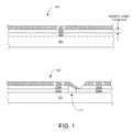
- FIGS. 2A-2Cdepict examples of laser polishing according to various embodiments by directing a pulsed laser beam to one or more sites on a surface.
- a substrate surface 201is depicted.
- the substratemay be a metal foil, such as a stainless steel foil, or a polymeric material.
- the substrate materialis a homogenous or non-homogenous composition of one or more metals, including steel, stainless steel, aluminum or titanium.
- the substrateis a polyimide material.
- Substrate surface 201is a normal appearing material surface after mechanical processing such as mechanical rolling, that is it contains high frequency roughness. To polish the substrate, a single laser pulse is directed at the surface.
- the absorbed energycreates a local melted region on the surface. This melted region expands, and a wave begins to move outward from the irradiated spot. Because the substrate is highly conductive, the thermal energy is lost quickly, resulting in a surface as depicted at 201 ′. The resulting surface feature represents a close approximation to a constant volume process. Because the material reaches a liquid state during the polishing process, any high frequency roughness (as present in surface 201 ) or other short wavelength features are lost due to the minimization of surface energy during the transitory liquid phase. The resultant lower frequency (longer wavelength) roughness is appropriate for film deposition and photovoltaic applications.
- FIG. 2Bdepicts a substrate surface 201 coated with an as-deposited back contact surface 203 .
- the substrate surfaceis not polished prior to depositing the back contact layer, though in other embodiments, the methods involve laser polishing the substrate surface prior to deposition of the back contact layer in addition to laser polishing the back contact layer surface.
- the back contactmay be molybdenum, niobium, chromium, or others, or combinations of these.
- FIG. 2Balso shows the back contact surface 203 ′ after a laser pulse treatment.
- the thickness of the back contactis sufficient to maintain the laser process within the back contact. For example, depending on the laser pulse energy, a back contact layer thickness of about 1-5 microns is sufficient to prevent the laser energy from affecting the underlying substrate surface.
- the laser polishing processcleans the surface in certain embodiments.
- FIG. 2Cshows a particle 204 and an organic smear 206 on a surface 202 .
- Surface 202may be a substrate surface or a back contact surface. If a 1 micron particle on a surface was left in place prior to coating the surface with a 1 micron film, significant discontinuities would be required to cover the particle. Particles larger than the overlying thickness cannot be fully covered. Both situations result in potential conductive paths to the back contact.
- a single laser pulseremoves the surface materials, with the polished section of the surface 202 ′ free of them.
- FIGS. 2A-2Care not-to-scale with the vertical scale much larger than the horizontal scale, such that the actual slopes are much shallower than they appear.
- Exposing the surface to a laser beam in accordance with the embodiments described hereinmay be performed in air, a controlled benign environment such as a noble gas (depending on the reactivity of the surface metal to air), in a reactive gas environment for incorporating elemental compositions into the surface material.
- a controlled benign environmentsuch as a noble gas (depending on the reactivity of the surface metal to air)
- a reactive gas environmentfor incorporating elemental compositions into the surface material.
- the compositions or elementsare placed on the surface prior to treatment for incorporation into the material during the melt phase. This is discussed further below.
- a substrateis provided in a web and thin-films are deposited on the substrate in a roll-to-roll process.
- the substrateis laser polished prior to the deposition of any films thereon.
- FIG. 3shows a simplified schematic diagram illustrating a top view of a laser polishing and deposition apparatus.
- a web 301 of a bare substrateis shown being unspooled to enter the first deposition chamber 304 .
- the manner in which the web is fed into the chamber, the orientation of a spool holding the web, the orientation of the deposition chambers, etc.may be varied.
- the webis vertical or near-vertical during laser polishing.
- the web materialis a thin metal foil such as stainless steel, though it may be a thin polymeric material.
- the web substratehas a width of between about 2 and 4 feet (in the direction perpendicular to the view), though the laser polishing apparatus may be configured to support substrates of any size, including sizes outside this range.
- the substrateis relatively low-cost, rolled sheet stock suitable for use as metallic or non-metallic substrates.
- metallic or non-metallic substratesinclude stainless steel, aluminum, titanium, alloys of aluminum or titanium, any metallic foil, or even a metalized non-metallic substrate.
- aluminum and titanium alloysinclude aluminum-silicon alloy and titanium-aluminum alloy, respectively;
- an example of a metalized non-metallic substrateis a flexible, non-conductive substrate, such as a polymer substrate, with a sputtered metallic layer; and an example of a stainless steel is 430-alloy stainless steel.
- the deposition surface of the substrate webPrior to passing into the first deposition chamber 304 , the deposition surface of the substrate web is irradiated with one or more laser beams at certain points on the surface at a laser polishing station 302 . This causes a melt pool to form at each of these points, evening out surface roughness as well as removing any particles that may be present on the material.
- the webpasses into multiple deposition chambers 304 , 306 and 308 , which contains one or more magnetrons and targets (not shown) for sputtering one or more thin-films on the web substrate.
- magnetrons and targetsfor sputtering one or more thin-films on the web substrate.
- molybdenum, copper or other back electrical contact materialmay be sputtered onto the substrate as it continuously moves through the deposition chamber 304 .
- Various guide rollersmay be used to guide the web substrate through the deposition chamber as well as throughout the apparatus.
- a deposition chambermay include a coating drum (not shown) to support the web substrate while it moves through the deposition chamber.
- the webis kept in constant tension throughout the machine, with rollers used as necessary to spread the web, provide web steering, provide web tension feedback to servo controllers, and to run the web in desired positions.
- the webthen passes into the next deposition chamber 306 for further thin-film deposition.
- a p-type CIGS layermay be deposited in this chamber.
- the webis transferred into deposition chamber 308 for deposition of the top layer or layers of the photovoltaic stack.
- a thin layer of n-type material to form and maintain the p-n junction in coordination with the previous layermay be deposited followed by deposition of a highly conductive and transparent aluminum doped ZnO layer that completes the top electrode.
- the deposition apparatus described aboveis an example of thin-film deposition apparatuses that may be used according to various embodiments.
- the number of deposition chambers usedmay range from one to as many as necessary to deposit the thin-film materials.
- the number, type and thickness of thin-films deposited in each chambermay also be varied depending on system implementation.
- each film described above with reference to FIG. 1may be deposited in one or more deposition chambers as appropriate.
- a single deposition chambermay be used to deposit multiple types of films.
- the active absorber stack deposited on the back contact layer after any of the methods described hereinmay include silicon (e.g. for amorphous, micro-crystalline, polycrystalline and tandem silicon cells), copper-indium-gallium-(selenium and/or sulfur), CdSe, CdTe, organic oligomers or polymers, layers of inorganic and organic materials, and whose final form may include micro-particles, nano-particles, or quantum dots.
- silicone.g. for amorphous, micro-crystalline, polycrystalline and tandem silicon cells
- CdSe, CdTeorganic oligomers or polymers
- layers of inorganic and organic materialsand whose final form may include micro-particles, nano-particles, or quantum dots.
- FIG. 3provides an example of a laser polishing apparatus in the context of a thin-film deposition apparatus
- cut pieces of substratesmay be polished rather than a substrate on a web.
- laser polishingis performed between unspooling of the roll and entering the deposition chamber
- polishingmay occur at a time and/or location remote from the deposition itself and may involve spooling the polished substrate.
- the back contactis polished either in addition to or in lieu of the substrate being polished. This may occur within a deposition apparatus, between deposition apparatuses, etc.
- each irradiated sitemay be between about 5 and 200 microns according to certain embodiments, for example, between about 5 and 100 microns, 5 and 25 microns, 5 and 50 microns, 100 and 200 microns or 150 and 200 microns.
- each irradiated siteis a single generally circular spot, having a diameter equal to the beam diameter at the surface.
- the beam areais defined by a lens that directs the beam on the substrate; in certain embodiments, the lens is shaped to direct ellipsoidal or other shaped spots on the substrate.
- the smoothed surfaceis characterized by interconnected surface features, with the features having a frequency of between about 1 and 200 microns, according to certain embodiments, for example, between about 5 and 200 microns about 5 and 100 microns, 5 and 25 microns, 5 and 50 microns, 100 and 200 microns or 150 and 200 microns.
- These interconnected surface featuresmay have a maximum aspect ratio of no more than 1:1.
- Pulse durationmay range from about 0.10-100 nanoseconds, e.g., 0.1-50 nanoseconds, 0.1-10 nanoseconds, or 1-10 nanoseconds.
- Peak pulse energymay range from about 1 microjoule to millijoules.
- Pulse wavelengthmay range from about 0.4-10 microns. These parameters may depend in part on the material surface being treated, as well as the desired textured surface that results.
- FIG. 4shows examples of high frequency roughness, low frequency roughness (waviness) and flatness scales.
- wavinesslow frequency roughness
- FIG. 4shows examples of surface roughness in film 402 .
- the images in FIG. 4are not shown to scale with the vertical scale exaggerated for illustrative purposes. Peaks 411 are present in the film with the peak-valley roughness being on the same order as the length scale, which ranges up to 10 microns.
- the aspect ratios (peak to valley vertical distance) of the features (peaks 411 )may be 1:1 or greater, e.g., 2:1, 3:1 or even higher. Further details of surface characteristics of as-received metallic substrates are described in U.S. Patent Publication No. 20090229666, incorporated by reference herein.
- the length scalesare greater than the peak to valley roughness, in certain cases at least an order of magnitude greater than the peak to valley roughness.
- the texturing methods described hereinmodify surfaces having high frequency, high aspect ratio (e.g., 1:1 or above) features, retexturing them so that they exhibit only low frequency or flat features as described above. It should be noted that unlike some technologies in which photolithography, multi-step CMP planarization, fly height control and other functional requirements demand controlled long-wavelength flatness, for thin-film photovoltaics, waviness is tolerable. Only the high aspect ratio surface features are disruptive to the film.
- overlapping texture patternsare formed by rastering one or more laser beams to irradiate multiple spots across an entire surface or a portion thereof.
- FIG. 5shows an example surface having a pattern of overlapping features created by laser reflow.
- a plan viewis shown at 510 , with features 512 overlapping in area 514 .
- a cross-sectional viewis shown at 520 .
- the beamis rastered back and forth in a linear fashion to form rows of features. An off-set is applied between rows to ensure complete coverage. To create overlap, the distance between irradiation points is smaller than the length scale of the resulting features.
- the features of the substrate patterninclude overlapping circular raised peripheries and a recessed center region. This is an example of an overlapping surface that may be formed.
- texturing a surface of a photovoltaic stack or a substratetherefore comprises creating features having aspect ratios, or height to diameter ratios of less than about 1, less than about 0.5, less than about 0.1, less than about 0.05, less than about 0.01, or less than about 0.005.
- FIG. 6is an image showing an example of a laser textured feature formed in a nickel surface. The feature has a height of 150 Angstroms and is 5 microns in diameter, a height to diameter ratio of less than 0.005. Note the long wavelength characteristics of the surface roughness, the continuity of the feature and the lack of local features in the region of the bump.
- FIG. 7Ashows two images of surface finishes of rolled or coined 300 series stainless steel surface prior to laser treatment.
- the imagesare 60 ⁇ 60 micron sized images, with a z-scale of 500 nm per division. Valleys are observed in both images (above left axis).
- FIG. 7Bshows an image of a surface finish of a 300 series stainless steel surface after laser treatment. The z-scale resolution is increased to 250 nm per division for additional clarity of the surface.
- the high frequency peaksare removed and a much gentler, more continuous surface results from laser treating. No valleys are observed after laser treating.
- texturing the substrate or back contact surfaceresults in substantially uniform features. These features may have substantially circular symmetry as depicted in FIG. 5 .
- the final surface of the meltincludes non-uniformities and/or non-circular symmetries. Pits, bumps, sombrero shapes and ellipsoidal shapes can be formed under specific conditions of beam size, shape, power intensity, pulse length, lens shape (spherical, cylindrical, etc.) and the like. In certain embodiments, an ellipsoidal pattern is achieved using a cylindrical front lens.
- FIG. 8shows two examples of texturing a surface of substrate 801 . At 810 , a rolled substrate 801 is depicted.
- the substrate surfacePrior to treatment, the substrate surface as directional features due to rolling (or other surface preparation) direction, which is indicated. Ellipsoidal features are created by using an appropriately shaped lens and/or relative motion between the beam and substrate in the direction of the major axis of the ellipse.
- a surface texture pattern having elongated laser features 812 in the longitudinal directionis depicted.
- a surface texture pattern having elongated laser features 812 in the cross-directionis depicted.
- the substrate and/or back contactis textured to produce a surface roughness that enhances light trapping.
- peak to peak distance between features tois between about 0.5 microns to about 1 micron, or about 0.5 microns to about 0.9 microns.
- texturing the substrate and/or back contactinvolves reducing peak height.
- laser polishing and retexturing techniques as described aboveare performed on a back contact layer.
- the back contact layeris molybdenum, niobium, chromium, copper, silver, or combinations of these or other suitable material for forming an ohmic contact.
- the back contact layerincludes molybdenum.
- the laser polishingmay be performed on the surface of the deposited back-contact, either exclusively or combined with a substrate polish, prior to the deposition of the remaining photovoltaic material set.
- FIG. 9provides a process flow chart illustrating certain operations in a method of laser polishing a back contact layer according to certain embodiments. First, a substrate is provided ( 901 ).
- the substratemay be provided in a web, e.g., a web of stainless steel material, or may be provided as cut sheets.
- the substratemay be a metallic foil or a conductive polymer material.
- the substrateis series 300 or series 400 stainless steel.
- the as-provided materialmay be machine rolled or otherwise pre-treated or worked. At the dimensions of interest to photovoltaic cells, machine rolled material exhibits high frequency roughness as described above with respect to FIG. 4 .
- the substrateis optionally polished ( 903 ). According to various embodiments, polishing involves laser polishing as described above. Alternatively, it may involve mechanical polishing, e.g., with an abrasive grit in lieu of or in addition to laser polishing.
- deposition of the back contactinvolves a physical vapor deposition or sputter process, though the methods are not so limited and encompass back contact films deposited by any suitable method.
- the thickness of the back contact filmis between about 0 and 5 microns, e.g., 1 and 5 microns. In certain embodiments, the back contact film thickness is about 5 microns or greater to allow suitable texturing and polishing depths. In certain embodiments, the back contact is less than 1 micron, e.g., about 0.5 microns. In these cases, the depth of the melt pools may be controlled to be relatively shallow, e.g., 10-100 Angstroms.
- laser polishinginvolves exposing multiple localized areas or sites of the back contact film to a laser beam having an intensity and for an exposure time sufficient to create a melt pool centered on each of the localized sites.
- the back contactis exposed to a laser beam to remove particles and organic material that may be present on the film surface or within the film.
- one or more laser beamsis rastered over the surface in a specific pattern to texture the surface as described above with respect to FIGS. 5-8 .
- polishing the as-deposited back contact layeralters the microstructure of the back contact layer from having a crystalline structure, or localized areas of crystalline structure, to a substantially amorphous material. In certain embodiments, this involves reducing the thickness of the layer. Also in certain embodiments, polishing the back contact enhances its diffusion barrier characteristics. That is, after polishing, the back contact lowers a diffusion coefficient for the absorber stack constituents, as well as for the constituents of the underlying substrate. In certain embodiments, at least the surface of the back contact is altered to be an amorphous material.
- an absorber layeris deposited on the back contact layer ( 909 ).
- adhesion of the CIGS or other absorber layeris improved by the laser polishing. The adhesion is improved by the presence of textured features and/or the presence of amorphous metal on the surface of the back contact.
- Polishing the back contactmay result in a superior surface for deposition of an absorber stack than polishing only the underlying substrate. For example, defects introduced during sputtering of the back contact onto a polished or unpolished substrate are eliminated by polishing the substrate.
- Another aspect of the inventioninvolves incorporating an element or compound into a substrate or back contact surface during a laser treatment process.
- sodiumis incorporated into a photovoltaic stack substrate and/or back contact during a laser polishing, cleaning or retexturing treatment.
- sodiumis incorporated into a substrate and/or back contact layer of a CIGS photovoltaic stack.
- Sodium diffusionhas been found to be advantageous during subsequent CIGS growth on the back contact as well as improve conductivity in the CIGS layer.
- FIGS. 10 and 11are process flow charts illustrating operations in methods of incorporating sodium into a CIGS photovoltaic stack according to various embodiments.
- a substrate for thin-film depositionis provided ( 1001 ).
- the substratemay be a metallic or conductive polymeric substrate.
- the substrateis an aluminum substrate or stainless steel.
- the substrateis then treated with sodium or a sodium containing compound ( 1003 ). Treating the substrate may involve exposing it to sodium vapor such that sodium absorbs onto the substrate, spraying, depositing or otherwise applying a coating of a metal salt to the substrate, applying a coating compound containing sodium to the substrate, etc.
- a thin layer of sodium or sodium containing compounde.g., NaF, NaCl, NaS, is deposited as a solid or precipitated as a liquid on the surface.
- a thin layer of a compound of metal and sodiumis deposited on the surface of the substrate.
- the sodium coated or treated substrateis then laser treated ( 1005 ).
- Laser treatinginvolves exposing the substrate to radiation from a laser beam at multiple spots across the substrate. This creates a melt pool of the sodium and substrate material at each spot, allowing incorporation of the sodium into the substrate surface. If a sodium-containing compound is used, laser treating dissociates the compound, with the sodium intermixed in the surface layers. The remaining byproducts (e.g., fluorine, chlorine, and the like) are reacted with a controlled reactive gas or getter system.
- operations 1003 and 1005overlap or are performed simultaneously.
- the substrateis exposed to an overpressure of sodium vapor or a sodium containing compound as it is irradiated. This results in the sodium being intermixed in the surface layers.
- the back contact layere.g., a molybdenum film
- An absorber layere.g., a CIGS layer
- the sodiumdiffuses from the substrate to the back contact, where it may diffuse from to reach the CIGS layer.
- the methodsinvolve forming a sodium concentration gradient in the substrate material, with the highest concentration at the top or front surface. This is possible due to the laser treatment of the substrate surface. Accordingly, in certain embodiments, the methods require less sodium. According to various embodiments, sodium is incorporated to be between about 0.5% and 5% by weight of the substrate.
- FIG. 11is process flow chart illustrating operations in another method of incorporating sodium into a CIGS stack in which the sodium is incorporated into the back contact layer in the same manners as described above for the substrate.
- a substrateis provided as described above ( 1101 ).
- the substratemay be polished or unpolished.
- a back contacte.g., a molybdenum thin-film, is then deposited on the substrate ( 1103 ).
- the back contactis then treated with sodium ( 1105 ). Treating the back contact may involve exposing it to sodium vapor such that sodium absorbs onto the back contact, spraying, depositing or otherwise applying a coating of a metal salt to the substrate, applying a coating compound containing sodium to the substrate, etc.
- a thin layer of sodium or sodium containing compounde.g., NaF, NaCl, NaS, is deposited as a solid or precipitated as a liquid on the back contact surface.
- a thin layer of a compound of metal and sodiumis deposited on the surface of the back contact
- the back contactthen undergoes laser treatment, to melt the molybdenum or back contact, and in certain cases sodium, thereby incorporating the sodium into the back contact ( 1107 ).
- operations 1105 and 1107overlap or are performed simultaneously.
- the back contactis exposed to an overpressure of a sodium vapor or a vapor of a sodium-containing compound as the back contact is irradiated.
- An absorber layere.g., a CIGS layer, is then deposited on the back contact ( 1109 ). The sodium diffuses from the substrate to the back contact, where it may diffuse from to reach the CIGS layer.
- the sodiummay be substantially uniformly incorporated in the back contact layer, or it may be incorporated such that there is a concentration gradient with the highest concentration at the top surface of the back contact layer.
- Other methods of incorporating sodium into the back contactgenerally involve the reverse concentration gradient, e.g., by supplying a sodium source such as lime glass at the back side of the metal contact.
- sodiumis incorporated to be between about 0.5% and 5% by weight of the back contact layer.
- oxygen or an oxygen-containing gasis flowed over the surface being polished to increase oxygen content in the polished film.
- a reducing gasis flowed over the surface to reduce the oxygen content.
- oxygen contentmay be controlled to control the mobility characteristics of species diffusing through molybdenum.
- FIGS. 12A and 12Bdepict an apparatus according to certain embodiments, with FIG. 12A showing a perspective view and FIG. 12B a side view of the apparatus.
- a web substrateis laser polished prior to entering a deposition apparatus.
- the apparatusis configured to laser treat a web substrate, e.g., a thin metal foil, and/or a back contact layer deposited on a web substrate.
- the web 1201is tensioned between two guide rollers 1204 a and 1204 b .
- Unpolished substrateis around roller 1204 a , polished substrate around roller 1204 b .
- one or both of the guide rollersmay not be present, e.g., they may be replaced with a spool.
- unpolished substratemay be taken off a spool, polished and then guided into a deposition apparatus as described above with respect to FIG. 3 .
- a laser source 1203emits a laser beam that is scanned in a cross-web direction by three galvo system 1206 .
- Individual beams 1214are emitted from each galvo system 1206 .
- the system, including web, laser source and galvo mirrorsare at a slight off-angle (mounting angle 1209 ) which may in certain embodiments, 1°-20° from vertical, or 5°-15° from vertical to ensure particulates and materials released from the laser process fall away from the film, and do not fall onto the galvo lenses.
- an air shower 1211is used together with gravity and an ionization system 1213 to further ensure continued clean operation across the entire web and to ensure the expulsion of released material.
- the galvo systems 1204may be spaced about one foot or less away from the web, and include galvo mirrors to raster the beam in a cross-web direction.
- one or more of the galvo systemsincludes a beam splitter to direct a beam to the next galvo system as well to the web. This allows, according to certain embodiments, a single laser source 1203 to be used with beam splitters in the galvo systems 1206 .
- the rastering processis in the near-vertical direction, while the web 1201 transverses along the length direction.
- One or more backside heating or cooling elements 1207is placed near or along the web to control the temperature as needed. According to various embodiments, backside temperature is controlled at a set level between about 0 and 100° C.
- the laser sourcemay be any of a single, double or quadrupled Nd:YAG or Nd:YLF laser, a carbon dioxide gas laser, and excimer source, or any other laser capable of producing the power (10-1000 W), power density (5-200 micron spot size), controlled pulse duration (0.1-100 ns) and repetition rate (100 kHz-1000 kHz) used for the treatment method.
- the laser wavelengthmay range from about 400 nm to 10 microns.
- the galvo systemsaccurately support adjacent spot placement tolerances of less than 5 microns, or less than 2 microns, at a repeating frequency of at least about 100 kHz. In alternate embodiments, multiple laser sources are used, or a single laser source and galvo system may be sufficient depending on the web size.
- FIGS. 13A and 13Billustrate a gas over-pressure system according to certain embodiments, which may be used to incorporate sodium or other components into a surface material.
- a split gas manifold 1315is positioned on either side of the laser beam 1314 .
- the manifold 1315extends across the web to flow gas in the proximity of the laser operation.
- a top view of the manifold 1315is depicted in FIG. 13B .
- the manifoldis configured to direct gas toward intersection of the laser beam 1314 and the web 1301 from either side of the laser beam 1314 .
Landscapes
- Engineering & Computer Science (AREA)
- Civil Engineering (AREA)
- Structural Engineering (AREA)
- Photovoltaic Devices (AREA)
Abstract
Description
- This application is a continuation-in-part of U.S. patent application Ser. No. 12/357,277, filed Jan. 21, 2009, which claims benefit of the following: U.S. Provisional Patent Application No. 61/022,232, filed Jan. 18, 2008 and U.S. Provisional Patent Application No. 61/022,240, filed Jan. 18, 2008. This application is also a continuation-in-part of U.S. patent application Ser. No. 12/049,159, filed Mar. 14, 2008. Each of these applications is incorporated by reference herein for all purposes.
- Solar cells are widely used to collect solar energy and generate electricity, with multiple solar cells interconnected to form solar panels. There are two main types of solar collectors: silicon and thin-film solar collectors. Silicon is currently the predominant technology, using silicon-based cells encapsulated behind glass. Thin-film processes involve depositing thin-film materials on a substrate to form a light absorbing layer sandwiched between electrical contact layers. The front or top contact is a transparent and conductive layer for current collection and light enhancement, the light absorbing layer is a semiconductor material, and the back contact is a conductive layer to provide electrical current throughout the cell.
- In one example of a fabrication process, a metallic back electrical contact layer is deposited on a substrate. A p-type semiconductor layer is then deposited on the back electrical contact layer and an n-type semiconductor layer is deposited on the p-type semiconductor layer to complete a p-n junction. Any suitable semiconductor materials, such as CIGS, CIS, CdTe, CdS, ZnS, ZnO, amorphous silicon, polycrystalline silicon, etc. may be used for these layers. A top transparent electrode layer is then deposited on the p-n junction. This layer may be a conductive oxide or other conductive film and is used for current collection. Once these or other materials have been deposited on the substrate to form a photovoltaic stack, the substrate and thin-film materials deposited may be cut into cells. Multiple cells are then assembled into a thin-film solar panel.
- Thin-film solar collectors are lower cost and require lower energy to produce. However, there are numerous sources of defects in a thin-film panel, given the materials used, the large surfaces areas required, the small thicknesses of films, and the sensitivity of the films to small particles. For example, a one micron particle is on the order of the film thickness. Defects from particles and other sources can cause shunts and otherwise compromise solar cell performance.
- Provided herein are methods of incorporating additives into thin-film solar cell substrates and back contacts. In certain embodiments, sodium is incorporated into a substrate or a back contact of a thin-film photovoltaic stack where it can diffuse into a CIGS or other absorber layer to improve efficiency and/or growth of the layer. The methods involve laser treating the substrate or back contact in the presence of a sodium (or sodium-containing) solid or vapor to thereby incorporate sodium into the surface of the substrate or back contact. In certain embodiments, the surface is simultaneously smoothed.
- One aspect of the invention relates to a method of incorporating sodium into a substrate of a thin-film photovoltaic stack, involving providing a substrate for thin-film photovoltaic stack; treating a front surface of the substrate with sodium; and irradiating the front surface with a plurality of laser beams at a plurality of spots on the substrate surface to thereby form molten mixtures of a substrate material and sodium; and solidifying the molten mixtures.
- In certain embodiments, the substrate is a metal substrate, e.g., a stainless steel foil. Treating the front surface of the substrate may involve any of depositing solid sodium (Na) on the front surface, depositing a solid sodium-containing compound such as NaF, NaCl, NaS, NaOH or any other compound on the front surface, precipitating a sodium-containing liquid on the surface, coating the surface with a sodium-containing solution or exposing the front surface to a sodium-containing vapor while irradiating the front surface with the plurality of laser beams. In certain embodiments, sodium is incorporated in the substrate such that there is a concentration gradient of sodium across a substrate thickness having a maximum at the front surface.
- Another aspect of the invention involves incorporating sodium into a back contact of a thin-film photovoltaic stack, involving providing a substrate for thin-film photovoltaic stack, said substrate having a thin-film back contact deposited thereon; treating a front surface of the back contact with sodium; irradiating the front surface with a plurality of laser beams at a plurality of spots on the back contact surface to thereby form molten mixtures of a back contact material and sodium; and solidifying the molten mixtures. In certain embodiments, the back contact is a molybdenum thin-film.
- Treating the front surface of the back contact may involve any of depositing solid sodium (Na) on the front surface, depositing a solid sodium-containing compound such as NaF, NaCl, NaS, NaOH or any other compound on the front surface, precipitating a sodium-containing liquid on the surface, coating the surface with a sodium-containing solution or exposing the front surface to a sodium-containing vapor while irradiating the front surface with the plurality of laser beams. In certain embodiments, sodium is incorporated in the back contact such that there is a concentration gradient of sodium across a back contact thickness having a maximum at the front surface.
- Another aspect of the invention relates to incorporating an additive into a substrate or back contact layer of a thin-film photovoltaic stack, involving providing a partially fabricated thin-film photovoltaic stack, said partially fabricated thin-film photovoltaic stack including at least a substrate; treating a front surface of the partially fabricated thin-film photovoltaic stack with an additive; irradiating the front surface with a plurality of laser beams at a plurality of spots on the substrate surface to thereby form molten mixtures of a substrate or back contact material and the additive; and solidifying the molten mixtures.
- These and other aspects of the invention are discussed in further detail below with reference to the figures.
- The accompanying drawings, which are incorporated in and form a part of this specification, illustrate embodiments of the invention and, together with the description, serve to explain the embodiments of the invention:
FIG. 1 depicts schematic illustrations of a thin-film solar cell and two monolithically integrated thin-film solar cells according to certain embodiments.FIG. 2A depicts a schematic illustration of laser polishing of a substrate of a thin-film photovoltaic stack according to certain embodiments.FIG. 2B depicts a schematic illustration of laser polishing of a back contact of a thin-film photovoltaic stack according to certain embodiments.FIG. 2C depicts a schematic illustration of laser cleaning of a surface of a layer in a thin-film photovoltaic stack according to certain embodiments.FIG. 3 is a simplified diagram showing a deposition apparatus for depositing thin film photovoltaic materials on a web substrate including a laser polishing apparatus according to certain embodiments.FIG. 4 depicts schematic illustrations of examples of high frequency roughness, low frequency roughness (waviness) and flatness scales of thin-film photovoltaic stacks according to certain embodiments.FIG. 5 depicts top and side views of an overlapping texture pattern according to certain embodiments.FIG. 6 is an image showing an example of a laser textured feature formed in a nickel surface.FIG. 7A shows two images of surface finishes of 300 series stainless steel surface prior to laser treatment.FIG. 7B shows an image of a surface finish of a 300 series stainless steel surface after laser treatment according to certain embodiments.FIG. 8 shows two examples of texturing a surface of substrate in an ellipsoidal pattern according to certain embodiments.FIG. 9 is a process flow diagram illustrating operations in a method of laser polishing or texturing a back contact film of a thin-film photovoltaic stack according to certain embodiments.FIGS. 10 and 11 are process flow diagrams illustrating operations in methods of incorporating sodium into a thin-film photovoltaic stack according to certain embodiments.FIGS. 12A and 12B depict components of a laser polishing apparatus according to certain embodiments.FIGS. 13A and 13B depict components of a laser treatment apparatus according to certain embodiments.- Thin-film solar panels have many advantages, including providing low cost, low energy production. However, there are numerous sources of defects in a thin-film panel, given materials used, the large surfaces areas required, the small thicknesses of films, and the sensitivity of the films to small particles. For example, a one micron particle is on the order of the film thickness. Defects from particles and other causes can cause shunts and otherwise compromise solar cell performance.
- Another factor related to defects is the level of substrate preparation. For semiconductor device fabrication, substrate (semiconductor wafer) preparation involves chemical-mechanical planarization and cleaning prior to wafers being released into the line. In media production, near sub-single nanometer polish levels are achieved. However, these techniques are highly complex and expensive in comparison to what can reasonably be done as pre-preparation prior to film deposition for a large area solar panel. Any large area, economical method of substrate preparation is likely to leave some level of high-frequency roughness, in comparison to the film thickness. As a result, any robust and high yielding thin-film solar product has a certain number of defects accounted for in the product and process design. Unlike wafer flatness requirements for photolithography, probing and other concerns, and magnetic media for spacing control, there are no significant waviness or flatness requirements for large area photovoltaic panels.
- However, defects and particles should be minimized as they can cause shunts between the top and back contacts of a photovoltaic stack. Shunt sites may be present on fabrication or can develop during the lifetime of a solar panel. This development can be related to moisture ingress, collection of ionic contaminants, changes in stress/strain in the film or package or thermal cycling. A new site near a collection line can sink nearly all current generated in a typical cell, and can actually melt the encapsulating material, allowing for additional environmental degradation. The use of serialized cell strings where the voltages are increased across an individual cell place even greater stresses on defect sites and film continuity, the opportunity for field damage to occur in a shaded or poor performing cell. In addition to shunt sites, other problematic results of film defects include low film performance due to poor junction formation and film delamination.
- Provided herein are methods of laser polishing, texturing and cleaning thin-film photovoltaic materials. Laser polishing as described herein refers to smoothing a surface of a substrate or back contact layer by exposing one or more localized areas or sites of the surface to laser irradiation, thereby creating a melt pool centered on the site of irradiation, and allowing the melted surface material to re-solidify. In certain embodiments, high frequency surface roughness is removed. In certain embodiments, surface waviness is removed.
- Laser texturing as described herein refers to a process of exposing a surface of a substrate or back contact layer to laser irradiation to create a surface pattern having long range order. Long range order refers to a substantially uniform pattern over a surface area of at least tens of square feet. In certain embodiments, laser texturing involves forming an interconnected low frequency patterned surface, the pattern surface frequency being between about 5 and 200 microns. In certain embodiments, the surface is provided having textured features from a rolling or other process. Such a surface may be retextured using laser irradiation. In certain embodiments, a laser textured surface may be characterized by one or more of: overlapping features, a substantially uniform array of features having a center-to-center distance of between about 5 and 200 microns, a substantially uniform array of features having circular symmetry, a substantially uniform array of features having non-circular symmetry, or a substantially uniform array of features having a center-to-center distance less than the natural length scale of the features. Laser texturing may involve rastering a laser beam in a first direction, while moving the surface in a second direction, such that features are formed across a surface at a 100-1000 kHz repetition rate.
- Laser cleaning as described herein refers to a process of removing organic or inorganic contamination from a surface of a substrate or back contact. The contamination may be in the form of discrete particles or may be in the form of smeared material.
- According to various embodiments, the methods involve removing defects from a material surface by rapidly heating the surface in an area of about 5-200 microns to form shallow (about 10-1000 angstroms deep) and rapidly expanding melt pools, followed by rapid cooling of the surface. The minimization of surface tension causes the surface to re-solidify in a locally smooth surface. That is, high frequency roughness is smoothed out, with a lower frequency bump or texture pattern remaining in certain embodiments after resolidification. Cooling of the surface may be active or passive according to various embodiments.
FIG. 1 includes a not-too-scale schematic of a thin-filmphotovoltaic stack 100 of a photovoltaic cell.Substrate 101 supports thin-film layers substrate 101 may be on the order of mils, the thickness of the thin-film stack on the order of microns (or hundredths of mils).Substrate 101 may be a metallic or polymeric material. According to various embodiments, thesubstrate 101 is relatively thin, such as for example, between about 2-100 mils, or in certain embodiments, 2-10 mils. However, other suitable thicknesses may also be used, e.g., 50 mils. Backelectrical contact layer 103 provides electrical contact to allow electrical current to flow through the photovoltaic cell, and may be made of any appropriate material, e.g., molybdenum, niobium, copper, silver, etc.Layer 107 is a top transparent electrode layer. In certain embodiments, it is a transparent conducting oxide (TCO), for example, zinc oxide, aluminum-doped zinc oxide and indium tin oxide.Layer 105 represents several thin-films deposited between backelectrical contact layer 103 and top transparentelectrical contact layer 107, including a p-n junction. To form the p-n junction, a p-type semiconductor layer is deposited on backelectrical contact layer 103 and an n-type semiconductor layer is deposited on the p-type semiconductor layer. According to various embodiments, any suitable semiconductor materials, such as CIGS, CIS, CdTe, CdS, ZnS, ZnO, amorphous silicon, polycrystalline silicon, etc. are used to form the p-n junction. For example, the p-type semiconductor layer may be CIGS or CIS, and the n-type semiconductor layer may be CdS or a cadmium free material, such as ZnS, ZnO, etc. Embodiments of the invention are not limited to these p-n junctions, but include any appropriate p-n junction produced either as a homojunction in a single semiconductor material, or alternatively as a heterojunction between two different semiconductor materials.- According to various embodiments, other thin-film layers may be deposited between the electrical contact layers103 and107. As an example, electrical contact layers103 and107 are separated by a distance of about 1-2 microns. Any ionic contamination and moisture, cutting defects (for non-monolithically integrated cells), conductive contamination, or film delamination can lead to shunting sites, resulting in manufacturing or latent defects. In particular, the presence of any defect in the substrate may cause shunting at the time of deposition, or make the stack susceptible to developing shunts.
FIG. 1 also depicts a not-to-scale schematic illustration of two monolithically integrated stacks at102. In this example, a first stack including thin-film layers film layers site 111, withtop contact layer 107aand back contact103bseparated into interconnected sections. Thesite 111 of film discontinuities is a likely point of moisture ingress, which can lead to shunting.- While there are various possible sources and causes of shunting and related defects, methods and apparatuses according to various embodiments remove or reduce a significant number of such causes. The photovoltaic thin-film stacks depicted in
FIG. 1 are deposited on a section of asubstrate 101 after it has been polished, and contains no substantial defects, particles, or areas of high roughness. As such no shunting between thetop contact layer 107 andmetal contact layer 103 and/orsubstrate 101 is observed. FIGS. 2A-2C depict examples of laser polishing according to various embodiments by directing a pulsed laser beam to one or more sites on a surface. First, inFIG. 2A , asubstrate surface 201 is depicted. The substrate may be a metal foil, such as a stainless steel foil, or a polymeric material. In certain embodiments, the substrate material is a homogenous or non-homogenous composition of one or more metals, including steel, stainless steel, aluminum or titanium. In another embodiment, the substrate is a polyimide material.Substrate surface 201 is a normal appearing material surface after mechanical processing such as mechanical rolling, that is it contains high frequency roughness. To polish the substrate, a single laser pulse is directed at the surface. The absorbed energy creates a local melted region on the surface. This melted region expands, and a wave begins to move outward from the irradiated spot. Because the substrate is highly conductive, the thermal energy is lost quickly, resulting in a surface as depicted at201′. The resulting surface feature represents a close approximation to a constant volume process. Because the material reaches a liquid state during the polishing process, any high frequency roughness (as present in surface201) or other short wavelength features are lost due to the minimization of surface energy during the transitory liquid phase. The resultant lower frequency (longer wavelength) roughness is appropriate for film deposition and photovoltaic applications. The slope of the raised feature inpolished surface 201′ created by the laser pulse is much less than the slopes of the unpolished features in201.FIG. 2B depicts asubstrate surface 201 coated with an as-depositedback contact surface 203. In the example shown, the substrate surface is not polished prior to depositing the back contact layer, though in other embodiments, the methods involve laser polishing the substrate surface prior to deposition of the back contact layer in addition to laser polishing the back contact layer surface. As described above, the back contact may be molybdenum, niobium, chromium, or others, or combinations of these.FIG. 2B also shows theback contact surface 203′ after a laser pulse treatment. In certain embodiments, the thickness of the back contact is sufficient to maintain the laser process within the back contact. For example, depending on the laser pulse energy, a back contact layer thickness of about 1-5 microns is sufficient to prevent the laser energy from affecting the underlying substrate surface.- In addition to retexturing the surface, the laser polishing process cleans the surface in certain embodiments. This is depicted in
FIG. 2C , which shows aparticle 204 and anorganic smear 206 on asurface 202.Surface 202 may be a substrate surface or a back contact surface. If a 1 micron particle on a surface was left in place prior to coating the surface with a 1 micron film, significant discontinuities would be required to cover the particle. Particles larger than the overlying thickness cannot be fully covered. Both situations result in potential conductive paths to the back contact. In the methods according to certain embodiments, a single laser pulse removes the surface materials, with the polished section of thesurface 202′ free of them. Because the initial part of the process involves a rapid influx of heat and expansion of the surrounding surface, most surface materials are easily removed. It should be noted that for illustration,FIGS. 2A-2C are not-to-scale with the vertical scale much larger than the horizontal scale, such that the actual slopes are much shallower than they appear. - Exposing the surface to a laser beam in accordance with the embodiments described herein may be performed in air, a controlled benign environment such as a noble gas (depending on the reactivity of the surface metal to air), in a reactive gas environment for incorporating elemental compositions into the surface material. In certain embodiments, the compositions or elements are placed on the surface prior to treatment for incorporation into the material during the melt phase. This is discussed further below.
- In certain embodiments, a substrate is provided in a web and thin-films are deposited on the substrate in a roll-to-roll process. According to various embodiments, the substrate is laser polished prior to the deposition of any films thereon. An example of a web path that includes laser polishing is described below with respect to
FIG. 3 , which shows a simplified schematic diagram illustrating a top view of a laser polishing and deposition apparatus. Aweb 301 of a bare substrate is shown being unspooled to enter thefirst deposition chamber 304. One of skill in the art will understand that the manner in which the web is fed into the chamber, the orientation of a spool holding the web, the orientation of the deposition chambers, etc., may be varied. As described below, in certain embodiments, the web is vertical or near-vertical during laser polishing. - In certain embodiments, the web material is a thin metal foil such as stainless steel, though it may be a thin polymeric material. In many embodiments, the web substrate has a width of between about 2 and 4 feet (in the direction perpendicular to the view), though the laser polishing apparatus may be configured to support substrates of any size, including sizes outside this range.
- In certain embodiments, the substrate is relatively low-cost, rolled sheet stock suitable for use as metallic or non-metallic substrates. These include stainless steel, aluminum, titanium, alloys of aluminum or titanium, any metallic foil, or even a metalized non-metallic substrate. Examples of aluminum and titanium alloys include aluminum-silicon alloy and titanium-aluminum alloy, respectively; an example of a metalized non-metallic substrate is a flexible, non-conductive substrate, such as a polymer substrate, with a sputtered metallic layer; and an example of a stainless steel is 430-alloy stainless steel.
- Prior to passing into the
first deposition chamber 304, the deposition surface of the substrate web is irradiated with one or more laser beams at certain points on the surface at alaser polishing station 302. This causes a melt pool to form at each of these points, evening out surface roughness as well as removing any particles that may be present on the material. - After polishing, the web passes into
multiple deposition chambers deposition chamber 304. Various guide rollers (not shown) may be used to guide the web substrate through the deposition chamber as well as throughout the apparatus. In certain embodiments, a deposition chamber may include a coating drum (not shown) to support the web substrate while it moves through the deposition chamber. In general, the web is kept in constant tension throughout the machine, with rollers used as necessary to spread the web, provide web steering, provide web tension feedback to servo controllers, and to run the web in desired positions. The web then passes into thenext deposition chamber 306 for further thin-film deposition. For example, a p-type CIGS layer may be deposited in this chamber. Next the web is transferred intodeposition chamber 308 for deposition of the top layer or layers of the photovoltaic stack. For example, a thin layer of n-type material to form and maintain the p-n junction in coordination with the previous layer may be deposited followed by deposition of a highly conductive and transparent aluminum doped ZnO layer that completes the top electrode. - The deposition apparatus described above is an example of thin-film deposition apparatuses that may be used according to various embodiments. The number of deposition chambers used may range from one to as many as necessary to deposit the thin-film materials. The number, type and thickness of thin-films deposited in each chamber may also be varied depending on system implementation. For example, each film described above with reference to
FIG. 1 may be deposited in one or more deposition chambers as appropriate. Likewise, a single deposition chamber may be used to deposit multiple types of films. - Still further, the active absorber stack deposited on the back contact layer after any of the methods described herein may include silicon (e.g. for amorphous, micro-crystalline, polycrystalline and tandem silicon cells), copper-indium-gallium-(selenium and/or sulfur), CdSe, CdTe, organic oligomers or polymers, layers of inorganic and organic materials, and whose final form may include micro-particles, nano-particles, or quantum dots.
- While
FIG. 3 provides an example of a laser polishing apparatus in the context of a thin-film deposition apparatus, one of skill in the art will understand that other the methods and apparatuses may be practiced with various modifications. For example, cut pieces of substrates may be polished rather than a substrate on a web. Also, while in certain embodiments, laser polishing is performed between unspooling of the roll and entering the deposition chamber, in other embodiments, polishing may occur at a time and/or location remote from the deposition itself and may involve spooling the polished substrate. In certain embodiments, the back contact is polished either in addition to or in lieu of the substrate being polished. This may occur within a deposition apparatus, between deposition apparatuses, etc. - The area of each irradiated site may be between about 5 and 200 microns according to certain embodiments, for example, between about 5 and 100 microns, 5 and 25 microns, 5 and 50 microns, 100 and 200 microns or 150 and 200 microns. In many embodiments, each irradiated site is a single generally circular spot, having a diameter equal to the beam diameter at the surface. The beam area is defined by a lens that directs the beam on the substrate; in certain embodiments, the lens is shaped to direct ellipsoidal or other shaped spots on the substrate.
- In certain embodiments, the smoothed surface is characterized by interconnected surface features, with the features having a frequency of between about 1 and 200 microns, according to certain embodiments, for example, between about 5 and 200 microns about 5 and 100 microns, 5 and 25 microns, 5 and 50 microns, 100 and 200 microns or 150 and 200 microns. These interconnected surface features may have a maximum aspect ratio of no more than 1:1.
- Pulse duration (full width half max peak power) may range from about 0.10-100 nanoseconds, e.g., 0.1-50 nanoseconds, 0.1-10 nanoseconds, or 1-10 nanoseconds. Peak pulse energy may range from about 1 microjoule to millijoules. Pulse wavelength may range from about 0.4-10 microns. These parameters may depend in part on the material surface being treated, as well as the desired textured surface that results.
- In certain embodiments, methods are provided for texturing the surface of a substrate for a thin-film photovoltaic stack. In certain embodiments, methods are provided for texturing the surface of a back contact layer of a thin-film photovoltaic stack.
FIG. 4 shows examples of high frequency roughness, low frequency roughness (waviness) and flatness scales. At410, is an example of surface roughness infilm 402. The images inFIG. 4 are not shown to scale with the vertical scale exaggerated for illustrative purposes.Peaks 411 are present in the film with the peak-valley roughness being on the same order as the length scale, which ranges up to 10 microns. The aspect ratios (peak to valley vertical distance) of the features (peaks411) may be 1:1 or greater, e.g., 2:1, 3:1 or even higher. Further details of surface characteristics of as-received metallic substrates are described in U.S. Patent Publication No. 20090229666, incorporated by reference herein. - At420, a
film 402 having a lower frequency roughness (waviness) with length scales (distance between features) of greater than 10 microns. Here, the length scales are greater than the peak to valley roughness, in certain cases at least an order of magnitude greater than the peak to valley roughness. At403, afilm 402 that is “flat” with length scales often exceeding a millimeter, is depicted. - According to various embodiments, the texturing methods described herein modify surfaces having high frequency, high aspect ratio (e.g., 1:1 or above) features, retexturing them so that they exhibit only low frequency or flat features as described above. It should be noted that unlike some technologies in which photolithography, multi-step CMP planarization, fly height control and other functional requirements demand controlled long-wavelength flatness, for thin-film photovoltaics, waviness is tolerable. Only the high aspect ratio surface features are disruptive to the film.
- In certain embodiments, overlapping texture patterns are formed by rastering one or more laser beams to irradiate multiple spots across an entire surface or a portion thereof.
FIG. 5 shows an example surface having a pattern of overlapping features created by laser reflow. A plan view is shown at510, withfeatures 512 overlapping inarea 514. A cross-sectional view is shown at520. In the depicted example, the beam is rastered back and forth in a linear fashion to form rows of features. An off-set is applied between rows to ensure complete coverage. To create overlap, the distance between irradiation points is smaller than the length scale of the resulting features. In the example depicted inFIG. 5 , the features of the substrate pattern include overlapping circular raised peripheries and a recessed center region. This is an example of an overlapping surface that may be formed. - According to various embodiments, texturing a surface of a photovoltaic stack or a substrate therefore comprises creating features having aspect ratios, or height to diameter ratios of less than about 1, less than about 0.5, less than about 0.1, less than about 0.05, less than about 0.01, or less than about 0.005.
FIG. 6 is an image showing an example of a laser textured feature formed in a nickel surface. The feature has a height of 150 Angstroms and is 5 microns in diameter, a height to diameter ratio of less than 0.005. Note the long wavelength characteristics of the surface roughness, the continuity of the feature and the lack of local features in the region of the bump. FIG. 7A shows two images of surface finishes of rolled or coined300 series stainless steel surface prior to laser treatment. The images are 60×60 micron sized images, with a z-scale of 500 nm per division. Valleys are observed in both images (above left axis).FIG. 7B shows an image of a surface finish of a 300 series stainless steel surface after laser treatment. The z-scale resolution is increased to 250 nm per division for additional clarity of the surface. As compared to the images inFIG. 7A , the high frequency peaks are removed and a much gentler, more continuous surface results from laser treating. No valleys are observed after laser treating.- In certain embodiments, texturing the substrate or back contact surface results in substantially uniform features. These features may have substantially circular symmetry as depicted in
FIG. 5 . In alternate embodiments, the final surface of the melt includes non-uniformities and/or non-circular symmetries. Pits, bumps, sombrero shapes and ellipsoidal shapes can be formed under specific conditions of beam size, shape, power intensity, pulse length, lens shape (spherical, cylindrical, etc.) and the like. In certain embodiments, an ellipsoidal pattern is achieved using a cylindrical front lens.FIG. 8 shows two examples of texturing a surface ofsubstrate 801. At810, a rolledsubstrate 801 is depicted. Prior to treatment, the substrate surface as directional features due to rolling (or other surface preparation) direction, which is indicated. Ellipsoidal features are created by using an appropriately shaped lens and/or relative motion between the beam and substrate in the direction of the major axis of the ellipse. At820, a surface texture pattern having elongated laser features812 in the longitudinal direction (in the direction of the surface preparation features) is depicted. At830, a surface texture pattern having elongated laser features812 in the cross-direction is depicted. - In certain embodiments, the substrate and/or back contact is textured to produce a surface roughness that enhances light trapping. In certain embodiments, peak to peak distance between features to is between about 0.5 microns to about 1 micron, or about 0.5 microns to about 0.9 microns. In certain embodiments, texturing the substrate and/or back contact involves reducing peak height.
- In certain embodiments, laser polishing and retexturing techniques as described above are performed on a back contact layer. In certain embodiments, the back contact layer is molybdenum, niobium, chromium, copper, silver, or combinations of these or other suitable material for forming an ohmic contact. In particular embodiments, the back contact layer includes molybdenum. The laser polishing may be performed on the surface of the deposited back-contact, either exclusively or combined with a substrate polish, prior to the deposition of the remaining photovoltaic material set.
FIG. 9 provides a process flow chart illustrating certain operations in a method of laser polishing a back contact layer according to certain embodiments. First, a substrate is provided (901). The substrate may be provided in a web, e.g., a web of stainless steel material, or may be provided as cut sheets. The substrate may be a metallic foil or a conductive polymer material. In certain embodiments, the substrate is series300 or series400 stainless steel. The as-provided material may be machine rolled or otherwise pre-treated or worked. At the dimensions of interest to photovoltaic cells, machine rolled material exhibits high frequency roughness as described above with respect toFIG. 4 . The substrate is optionally polished (903). According to various embodiments, polishing involves laser polishing as described above. Alternatively, it may involve mechanical polishing, e.g., with an abrasive grit in lieu of or in addition to laser polishing. The substrate is then provided to a deposition chamber, for deposition of the back contact thin-film thereon (905). In many embodiments, deposition of the back contact involves a physical vapor deposition or sputter process, though the methods are not so limited and encompass back contact films deposited by any suitable method. - According to various embodiments, the thickness of the back contact film is between about 0 and 5 microns, e.g., 1 and 5 microns. In certain embodiments, the back contact film thickness is about 5 microns or greater to allow suitable texturing and polishing depths. In certain embodiments, the back contact is less than 1 micron, e.g., about 0.5 microns. In these cases, the depth of the melt pools may be controlled to be relatively shallow, e.g., 10-100 Angstroms.
- Once the back contact film is deposited, laser polishing is performed (907). As described above, laser polishing involves exposing multiple localized areas or sites of the back contact film to a laser beam having an intensity and for an exposure time sufficient to create a melt pool centered on each of the localized sites. According to various embodiments, the back contact is exposed to a laser beam to remove particles and organic material that may be present on the film surface or within the film. Also, according to various embodiments, one or more laser beams is rastered over the surface in a specific pattern to texture the surface as described above with respect to
FIGS. 5-8 . - In certain embodiments, polishing the as-deposited back contact layer alters the microstructure of the back contact layer from having a crystalline structure, or localized areas of crystalline structure, to a substantially amorphous material. In certain embodiments, this involves reducing the thickness of the layer. Also in certain embodiments, polishing the back contact enhances its diffusion barrier characteristics. That is, after polishing, the back contact lowers a diffusion coefficient for the absorber stack constituents, as well as for the constituents of the underlying substrate. In certain embodiments, at least the surface of the back contact is altered to be an amorphous material.
- After the back contact film is polished and, in certain embodiments, retextured, an absorber layer is deposited on the back contact layer (909). In certain embodiments, adhesion of the CIGS or other absorber layer is improved by the laser polishing. The adhesion is improved by the presence of textured features and/or the presence of amorphous metal on the surface of the back contact.
- Polishing the back contact may result in a superior surface for deposition of an absorber stack than polishing only the underlying substrate. For example, defects introduced during sputtering of the back contact onto a polished or unpolished substrate are eliminated by polishing the substrate.
- Another aspect of the invention involves incorporating an element or compound into a substrate or back contact surface during a laser treatment process. In certain embodiments, sodium is incorporated into a photovoltaic stack substrate and/or back contact during a laser polishing, cleaning or retexturing treatment. In particular embodiments, sodium is incorporated into a substrate and/or back contact layer of a CIGS photovoltaic stack. Sodium diffusion has been found to be advantageous during subsequent CIGS growth on the back contact as well as improve conductivity in the CIGS layer.
FIGS. 10 and 11 are process flow charts illustrating operations in methods of incorporating sodium into a CIGS photovoltaic stack according to various embodiments. First, inFIG. 10 , a substrate for thin-film deposition is provided (1001). The substrate may be a metallic or conductive polymeric substrate. In certain embodiments, the substrate is an aluminum substrate or stainless steel. The substrate is then treated with sodium or a sodium containing compound (1003). Treating the substrate may involve exposing it to sodium vapor such that sodium absorbs onto the substrate, spraying, depositing or otherwise applying a coating of a metal salt to the substrate, applying a coating compound containing sodium to the substrate, etc. In certain embodiments, a thin layer of sodium or sodium containing compound, e.g., NaF, NaCl, NaS, is deposited as a solid or precipitated as a liquid on the surface. In certain embodiments, a thin layer of a compound of metal and sodium is deposited on the surface of the substrate.- The sodium coated or treated substrate is then laser treated (1005). Laser treating involves exposing the substrate to radiation from a laser beam at multiple spots across the substrate. This creates a melt pool of the sodium and substrate material at each spot, allowing incorporation of the sodium into the substrate surface. If a sodium-containing compound is used, laser treating dissociates the compound, with the sodium intermixed in the surface layers. The remaining byproducts (e.g., fluorine, chlorine, and the like) are reacted with a controlled reactive gas or getter system. In certain embodiments,
operations - The back contact layer, e.g., a molybdenum film, is then deposited on the substrate (1007). An absorber layer, e.g., a CIGS layer, is then deposited on the back contact (1009). The sodium diffuses from the substrate to the back contact, where it may diffuse from to reach the CIGS layer.
- In certain embodiments, the methods involve forming a sodium concentration gradient in the substrate material, with the highest concentration at the top or front surface. This is possible due to the laser treatment of the substrate surface. Accordingly, in certain embodiments, the methods require less sodium. According to various embodiments, sodium is incorporated to be between about 0.5% and 5% by weight of the substrate.
FIG. 11 is process flow chart illustrating operations in another method of incorporating sodium into a CIGS stack in which the sodium is incorporated into the back contact layer in the same manners as described above for the substrate. In this method, a substrate is provided as described above (1101). The substrate may be polished or unpolished. A back contact, e.g., a molybdenum thin-film, is then deposited on the substrate (1103). The back contact is then treated with sodium (1105). Treating the back contact may involve exposing it to sodium vapor such that sodium absorbs onto the back contact, spraying, depositing or otherwise applying a coating of a metal salt to the substrate, applying a coating compound containing sodium to the substrate, etc. In certain embodiments, a thin layer of sodium or sodium containing compound, e.g., NaF, NaCl, NaS, is deposited as a solid or precipitated as a liquid on the back contact surface. In certain embodiments, a thin layer of a compound of metal and sodium is deposited on the surface of the back contact- The back contact then undergoes laser treatment, to melt the molybdenum or back contact, and in certain cases sodium, thereby incorporating the sodium into the back contact (1107). In certain embodiments, operations1105 and1107 overlap or are performed simultaneously. For example, in certain embodiments, the back contact is exposed to an overpressure of a sodium vapor or a vapor of a sodium-containing compound as the back contact is irradiated. An absorber layer, e.g., a CIGS layer, is then deposited on the back contact (1109). The sodium diffuses from the substrate to the back contact, where it may diffuse from to reach the CIGS layer.
- According to various embodiments, the sodium may be substantially uniformly incorporated in the back contact layer, or it may be incorporated such that there is a concentration gradient with the highest concentration at the top surface of the back contact layer. Other methods of incorporating sodium into the back contact generally involve the reverse concentration gradient, e.g., by supplying a sodium source such as lime glass at the back side of the metal contact. According to various embodiments, sodium is incorporated to be between about 0.5% and 5% by weight of the back contact layer.
- While the above examples refer to incorporation of sodium into the substrate and/or back contact layer, other elements or compounds may be incorporated in addition to or instead of sodium. These compounds may be coated on or otherwise applied as described above. In certain embodiments, a noble or reactive gas is used in conjunction with the laser process to control the final material composition in the solidified substrate or back contact melt. An example of an apparatus to implement this aspect of the invention is described below with reference to
FIGS. 13A and 13B . - In a particular example, oxygen or an oxygen-containing gas is flowed over the surface being polished to increase oxygen content in the polished film. In another example, a reducing gas is flowed over the surface to reduce the oxygen content. For example, oxygen content may be controlled to control the mobility characteristics of species diffusing through molybdenum.
- Provided herein are apparatuses for carrying out the above-described methods. The methods may also be performed with other laser systems.
FIGS. 12A and 12B depict an apparatus according to certain embodiments, withFIG. 12A showing a perspective view andFIG. 12B a side view of the apparatus. As described above, in certain embodiments, a web substrate is laser polished prior to entering a deposition apparatus. The apparatus is configured to laser treat a web substrate, e.g., a thin metal foil, and/or a back contact layer deposited on a web substrate. - In the figures, the
web 1201 is tensioned between twoguide rollers roller 1204a, polished substrate aroundroller 1204b. In certain embodiments, one or both of the guide rollers may not be present, e.g., they may be replaced with a spool. For example, in certain embodiments, unpolished substrate may be taken off a spool, polished and then guided into a deposition apparatus as described above with respect toFIG. 3 . - A
laser source 1203 emits a laser beam that is scanned in a cross-web direction by threegalvo system 1206.Individual beams 1214 are emitted from eachgalvo system 1206. The system, including web, laser source and galvo mirrors are at a slight off-angle (mounting angle1209) which may in certain embodiments, 1°-20° from vertical, or 5°-15° from vertical to ensure particulates and materials released from the laser process fall away from the film, and do not fall onto the galvo lenses. - In certain embodiments, an
air shower 1211 is used together with gravity and anionization system 1213 to further ensure continued clean operation across the entire web and to ensure the expulsion of released material. The galvo systems1204 may be spaced about one foot or less away from the web, and include galvo mirrors to raster the beam in a cross-web direction. In certain embodiments in which multiple galvo systems are used, one or more of the galvo systems includes a beam splitter to direct a beam to the next galvo system as well to the web. This allows, according to certain embodiments, asingle laser source 1203 to be used with beam splitters in thegalvo systems 1206. The rastering process is in the near-vertical direction, while theweb 1201 transverses along the length direction. One or more backside heating orcooling elements 1207 is placed near or along the web to control the temperature as needed. According to various embodiments, backside temperature is controlled at a set level between about 0 and 100° C. - Using multiple lasers, or a single laser with split beams, and multiple galvo systems increase system throughput. The laser source may be any of a single, double or quadrupled Nd:YAG or Nd:YLF laser, a carbon dioxide gas laser, and excimer source, or any other laser capable of producing the power (10-1000 W), power density (5-200 micron spot size), controlled pulse duration (0.1-100 ns) and repetition rate (100 kHz-1000 kHz) used for the treatment method. The laser wavelength may range from about 400 nm to 10 microns. The galvo systems accurately support adjacent spot placement tolerances of less than 5 microns, or less than 2 microns, at a repeating frequency of at least about 100 kHz. In alternate embodiments, multiple laser sources are used, or a single laser source and galvo system may be sufficient depending on the web size.
FIGS. 13A and 13B illustrate a gas over-pressure system according to certain embodiments, which may be used to incorporate sodium or other components into a surface material. Asplit gas manifold 1315 is positioned on either side of thelaser beam 1314. The manifold1315 extends across the web to flow gas in the proximity of the laser operation. A top view of the manifold1315 is depicted inFIG. 13B . The manifold is configured to direct gas toward intersection of thelaser beam 1314 and theweb 1301 from either side of thelaser beam 1314.- The foregoing descriptions of specific embodiments of the present invention have been presented for purposes of illustration and description. They are not intended to be exhaustive or to limit the invention to the precise forms disclosed, and many modifications and variations are possible in light of the above teaching. The embodiments described herein were chosen and described in order to best explain the principles of the invention and its practical application, to thereby enable others skilled in the art to best utilize the invention and various embodiments with various modifications as are suited to the particular use contemplated. It is intended that the scope of the invention be defined by the claims appended hereto and their equivalents.
Claims (25)
Priority Applications (1)
| Application Number | Priority Date | Filing Date | Title |
|---|---|---|---|
| US12/820,560US8586398B2 (en) | 2008-01-18 | 2010-06-22 | Sodium-incorporation in solar cell substrates and contacts |
Applications Claiming Priority (5)
| Application Number | Priority Date | Filing Date | Title |
|---|---|---|---|
| US2224008P | 2008-01-18 | 2008-01-18 | |
| US2223208P | 2008-01-18 | 2008-01-18 | |
| US12/049,159US20090229666A1 (en) | 2008-03-14 | 2008-03-14 | Smoothing a metallic substrate for a solar cell |
| US12/357,277US20090183764A1 (en) | 2008-01-18 | 2009-01-21 | Detachable Louver System |
| US12/820,560US8586398B2 (en) | 2008-01-18 | 2010-06-22 | Sodium-incorporation in solar cell substrates and contacts |
Related Parent Applications (1)
| Application Number | Title | Priority Date | Filing Date |
|---|---|---|---|
| US12/357,277Continuation-In-PartUS20090183764A1 (en) | 2008-01-18 | 2009-01-21 | Detachable Louver System |
Publications (2)
| Publication Number | Publication Date |
|---|---|
| US20100255630A1true US20100255630A1 (en) | 2010-10-07 |
| US8586398B2 US8586398B2 (en) | 2013-11-19 |
Family
ID=42826524
Family Applications (1)
| Application Number | Title | Priority Date | Filing Date |
|---|---|---|---|
| US12/820,560Active2029-09-11US8586398B2 (en) | 2008-01-18 | 2010-06-22 | Sodium-incorporation in solar cell substrates and contacts |
Country Status (1)
| Country | Link |
|---|---|
| US (1) | US8586398B2 (en) |
Cited By (6)
| Publication number | Priority date | Publication date | Assignee | Title |
|---|---|---|---|---|
| US20100258982A1 (en)* | 2008-01-18 | 2010-10-14 | Miasole | Laser polishing of a solar cell substrate |
| US20100258542A1 (en)* | 2008-01-18 | 2010-10-14 | Miasole | Laser polishing of a back contact of a solar cell |
| US20120240989A1 (en)* | 2010-10-01 | 2012-09-27 | Stion Corporation | Method and Device for Cadmium-Free Solar Cells |
| US8586398B2 (en)* | 2008-01-18 | 2013-11-19 | Miasole | Sodium-incorporation in solar cell substrates and contacts |
| US20140308774A1 (en)* | 2010-10-01 | 2014-10-16 | Stion Corporation | Method and device for cadmium-free solar cells |
| US20210035767A1 (en)* | 2019-07-29 | 2021-02-04 | Applied Materials, Inc. | Methods for repairing a recess of a chamber component |
Citations (83)
| Publication number | Priority date | Publication date | Assignee | Title |
|---|---|---|---|---|
| US2218913A (en)* | 1938-01-18 | 1940-10-22 | John M Hughes | Apparatus for scrubbing and polishing strip metal |
| US3810786A (en)* | 1970-04-15 | 1974-05-14 | Nyby Bruk Ab | Method for cleaning (degreasing) web material |
| US3952180A (en)* | 1974-12-04 | 1976-04-20 | Avco Everett Research Laboratory, Inc. | Cladding |
| US4015100A (en)* | 1974-01-07 | 1977-03-29 | Avco Everett Research Laboratory, Inc. | Surface modification |
| US4122240A (en)* | 1976-02-17 | 1978-10-24 | United Technologies Corporation | Skin melting |
| US4328390A (en)* | 1979-09-17 | 1982-05-04 | The University Of Delaware | Thin film photovoltaic cell |
| US4464479A (en)* | 1982-04-28 | 1984-08-07 | Rheinische Braunkohlenwerke Ag | Method for treating red mud |
| US4639543A (en)* | 1985-02-04 | 1987-01-27 | Richard J. Birch | Semiconductor devices having a metallic glass substrate |
| US4731516A (en)* | 1985-10-11 | 1988-03-15 | Mitsubishi Denki Kabushiki Kaisha | Laser polishing semiconductor wafer |
| US4789438A (en)* | 1987-06-23 | 1988-12-06 | Olin Corporation | Cathode surface treatment for electroforming metallic foil or strip |
| US4968383A (en)* | 1985-06-18 | 1990-11-06 | The Dow Chemical Company | Method for molding over a preform |
| US5038950A (en)* | 1989-07-14 | 1991-08-13 | Kabushiki Kaisha Toshiba | Method and apparatus for joining together associated metal conductors of a layer structure with an insulating layer provided therebetween |
| US5142778A (en)* | 1991-03-13 | 1992-09-01 | United Technologies Corporation | Gas turbine engine component repair |
| US5232674A (en)* | 1989-12-20 | 1993-08-03 | Fujitsu Limited | Method of improving surface morphology of laser irradiated surface |
| US5287622A (en)* | 1986-12-17 | 1994-02-22 | Canon Kabushiki Kaisha | Method for preparation of a substrate for a heat-generating device, method for preparation of a heat-generating substrate, and method for preparation of an ink jet recording head |
| US5407702A (en)* | 1993-05-05 | 1995-04-18 | Aluminum Company Of America | Method for coating a metal strip |
| US5532520A (en)* | 1993-06-22 | 1996-07-02 | Kabushiki Kaisha Toshiba | Semiconductor wafer with alignment marks |
| US5558759A (en)* | 1994-07-26 | 1996-09-24 | Sargent Manufacturing Company | Metal finishing process |
| US5821597A (en)* | 1992-09-11 | 1998-10-13 | Semiconductor Energy Laboratory Co., Ltd. | Photoelectric conversion device |
| US5843117A (en)* | 1996-02-14 | 1998-12-01 | Inflow Dynamics Inc. | Implantable vascular and endoluminal stents and process of fabricating the same |
| US5935307A (en)* | 1997-04-10 | 1999-08-10 | Parks; Katherine D. | Compositions and methods for incorporating alloying compounds into metal substrates |
| US6048255A (en)* | 1995-08-22 | 2000-04-11 | Seagate Technology, Inc. | Pulsed laser surface treatments for magnetic recording media |
| US6113753A (en)* | 1999-03-23 | 2000-09-05 | Flextor, Inc. | Systems and methods for making a magnetic recording medium on a flexible metal substrate |
| US6143095A (en)* | 1997-07-29 | 2000-11-07 | Korea Atomic Energy Research Institute | Method for surface-alloying on metal or alloy substrates, or for surface-repairing the damaged (or failed) metal or alloy substrates using a laser beam |
| US6156997A (en)* | 1995-05-31 | 2000-12-05 | Semiconductor Energy Laboratory Co., Ltd. | Laser processing method and laser processing apparatus |
| US6205830B1 (en)* | 2000-02-24 | 2001-03-27 | The Material Works, Ltd. | Method and apparatus for processing sheet metal |
| US6249503B1 (en)* | 1997-08-08 | 2001-06-19 | Sony Corporation | Method of and apparatus for recording/reproducing an information signal, recording/reproducing head device, memory medium, and head element |
| US6251002B1 (en)* | 1995-11-16 | 2001-06-26 | 3M Innovative Properties Company | Surface treating articles and method of making same |
| US6492615B1 (en)* | 2000-10-12 | 2002-12-10 | Scimed Life Systems, Inc. | Laser polishing of medical devices |
| US20020193870A1 (en)* | 1996-04-26 | 2002-12-19 | Jang G. David | Intravascular stent |
| US6504127B1 (en)* | 1999-09-30 | 2003-01-07 | National Research Council Of Canada | Laser consolidation methodology and apparatus for manufacturing precise structures |
| US20030019853A1 (en)* | 2001-07-24 | 2003-01-30 | Hayen Fredrick V. | Method of laser polishing surfaces on a head suspension assembly |
| US6521862B1 (en)* | 2001-10-09 | 2003-02-18 | International Business Machines Corporation | Apparatus and method for improving chamfer quality of disk edge surfaces with laser treatment |
| US20030068518A1 (en)* | 2001-08-07 | 2003-04-10 | Northeastern University And Trustees Of Tufts College | Process of forming a composite coating on a substrate |
| US6700096B2 (en)* | 2001-10-30 | 2004-03-02 | Semiconductor Energy Laboratory Co., Ltd. | Laser apparatus, laser irradiation method, manufacturing method for semiconductor device, semiconductor device, production system for semiconductor device using the laser apparatus, and electronic equipment |
| US6717105B1 (en)* | 2000-11-02 | 2004-04-06 | Mitsubishi Denki Kabushiki Kaisha | Laser annealing optical system and laser annealing apparatus using the same |
| US20040069751A1 (en)* | 2002-10-07 | 2004-04-15 | Shunpei Yamazaki | Method of irradiating laser, laser irradiation system, and manufacturing method of semiconductor device |
| US6727083B2 (en)* | 1999-03-19 | 2004-04-27 | Sumitomo Chemical Company, Limited | Protein capable of catalyzing transamination stereoselectively, gene encoding said protein and use thereof |
| US6733931B2 (en)* | 2002-03-13 | 2004-05-11 | Sharp Laboratories Of America, Inc. | Symmetrical mask system and method for laser irradiation |
| US6852012B2 (en)* | 2000-03-17 | 2005-02-08 | Wafer Solutions, Inc. | Cluster tool systems and methods for in fab wafer processing |
| US20050038551A1 (en)* | 2002-08-29 | 2005-02-17 | Jyoti Mazumder | Method of fabricating composite tooling using closed-loop direct-metal deposition |
| US6861407B2 (en)* | 2000-07-12 | 2005-03-01 | The Board Of Regents, The University Of Texas System | Methods of therapy with thrombin derived peptides |
| US20050074915A1 (en)* | 2001-07-13 | 2005-04-07 | Tuttle John R. | Thin-film solar cell fabricated on a flexible metallic substrate |
| US20050081367A1 (en)* | 2003-10-21 | 2005-04-21 | Lauinger Geoffrey A. | Method of manufacturing a media reference surface for use in a flexible data storage card |
| US6887124B2 (en)* | 2000-04-05 | 2005-05-03 | Applied Materials, Inc. | Method of polishing and cleaning substrates |
| US6908362B2 (en)* | 2001-03-02 | 2005-06-21 | Superpower, Inc | Reel-to-reel substrate tape polishing system |
| US6944195B2 (en)* | 1999-02-12 | 2005-09-13 | Semiconductor Energy Laboratory Co., Ltd. | Laser irradiation method, laser irradiation apparatus, and semiconductor device |
| US20050252894A1 (en)* | 2001-11-12 | 2005-11-17 | Sony Corporation | Laser annealing device and method for producing thin-film transistor |
| US20060081573A1 (en)* | 2002-06-27 | 2006-04-20 | Fraunhofer-Gesellschaft Zur Foderung Der Angewandten Forschung E.V. | Method for smoothing and polishing surfaces by treating them with energetic radiation |
| US20060091546A1 (en)* | 2004-10-07 | 2006-05-04 | Siemens Aktiengsellschaft | Layer system |
| US7081043B2 (en)* | 2004-01-14 | 2006-07-25 | 3M Innovative Properties Company | Molded abrasive brush and methods of using for manufacture of printed circuit boards |
| US20060166470A1 (en)* | 2001-11-16 | 2006-07-27 | Semiconductor Energy Laboratory Co., Ltd. | Method of irradiating a laser beam, apparatus for irradiating a laser beam and method of fabricating semiconductor devices |
| US7169286B2 (en)* | 2003-07-01 | 2007-01-30 | Superpower, Inc. | Process control methods of electropolishing for metal substrate preparation in producing YBCO coated conductors |
| US20070036994A1 (en)* | 2003-09-17 | 2007-02-15 | Bernard Andre | Multiple zone structure capable of light radiation annealing and method using said structure |
| US7192479B2 (en)* | 2002-04-17 | 2007-03-20 | Sharp Laboratories Of America, Inc. | Laser annealing mask and method for smoothing an annealed surface |
| US7207862B2 (en)* | 2002-02-28 | 2007-04-24 | Ebara Corporation | Polishing apparatus and method for detecting foreign matter on polishing surface |
| US20070140325A1 (en)* | 2004-12-10 | 2007-06-21 | Stmicroelectronics S.R.L. | Method and system for improving modem performance, computer program product therefor |
| US20070158315A1 (en)* | 2004-07-30 | 2007-07-12 | Semiconductor Energy Laboratory Co., Ltd. | Laser irradiation apparatus and laser irradiation method |
| US20080009093A1 (en)* | 2006-07-07 | 2008-01-10 | Chen-Kuei Chung | Silicon material having a mark on the surface thereof and the method of making the same |
| US20080196756A1 (en)* | 2007-01-22 | 2008-08-21 | Basol Bulent M | Roll-to-roll integration of thin film solar modules |
| US20080223832A1 (en)* | 2006-11-16 | 2008-09-18 | Lijun Song | Real time implementation of generalized predictive control algorithm for the control of direct metal deposition (dmd) process |
| US20080264910A1 (en)* | 2004-09-14 | 2008-10-30 | Raman Kashyap | Process for Fabricating Optical Waveguides |
| US20080280541A1 (en)* | 2007-05-10 | 2008-11-13 | 3M Innovative Properties Company | Abrasive filament and brush |
| US7504604B2 (en)* | 2002-11-29 | 2009-03-17 | Leica Geosystems Ag | Method for soldering miniaturized components to a baseplate |
| US20090078313A1 (en)* | 2007-09-18 | 2009-03-26 | Basol Bulent M | Substrate preparation for thin film solar cell manufacturing |
| US20090183760A1 (en)* | 2008-01-18 | 2009-07-23 | Tenksolar Inc | Redundant electrical architecture for photovoltaic modules |
| US20090183763A1 (en)* | 2008-01-18 | 2009-07-23 | Tenksolar, Inc | Flat-Plate Photovoltaic Module |
| US20090183764A1 (en)* | 2008-01-18 | 2009-07-23 | Tenksolar, Inc | Detachable Louver System |
| US20090229666A1 (en)* | 2008-03-14 | 2009-09-17 | Jason Stephan Corneille | Smoothing a metallic substrate for a solar cell |
| US20090266399A1 (en)* | 2008-04-28 | 2009-10-29 | Basol Bulent M | Metallic foil substrate and packaging technique for thin film solar cells and modules |
| US20100131108A1 (en)* | 2008-01-18 | 2010-05-27 | Tenksolar, Inc | Thin-film photovoltaic module |
| US7737054B2 (en)* | 2003-03-17 | 2010-06-15 | Semiconductor Energy Laboratory Co., Ltd. | Laser irradiation apparatus, laser irradiation method, and method for manufacturing a semiconductor device |
| US20100212720A1 (en)* | 2009-02-23 | 2010-08-26 | Tenksolar, Inc. | Highly efficient renewable energy system |
| US20100258542A1 (en)* | 2008-01-18 | 2010-10-14 | Miasole | Laser polishing of a back contact of a solar cell |
| US20100258185A1 (en)* | 2008-01-18 | 2010-10-14 | Miasole | Textured substrate for thin-film solar cell |
| US20100258158A1 (en)* | 2007-10-16 | 2010-10-14 | Saint-Gobain Glass France | Made to elements capable of collecting light |
| US20100258173A1 (en)* | 2009-04-13 | 2010-10-14 | Joseph Laia | Polishing a thin metallic substrate for a solar cell |
| US20100258982A1 (en)* | 2008-01-18 | 2010-10-14 | Miasole | Laser polishing of a solar cell substrate |
| US20100282276A1 (en)* | 2009-04-13 | 2010-11-11 | Miasole | Removing defects from photovoltaic cell metallic substrates with fixed-abrasive filament roller brushes |
| US20100282293A1 (en)* | 2009-01-21 | 2010-11-11 | Tenksolar | Illumination agnostic solar panel |
| US7903336B2 (en)* | 2005-10-11 | 2011-03-08 | Gsi Group Corporation | Optical metrological scale and laser-based manufacturing method therefor |
| US7947575B2 (en)* | 2006-11-27 | 2011-05-24 | Electro Scientific Industries, Inc. | Laser machining |
| US20120204935A1 (en)* | 2010-02-23 | 2012-08-16 | Tenksolar | Highly efficient solar arrays |
Family Cites Families (12)
| Publication number | Priority date | Publication date | Assignee | Title |
|---|---|---|---|---|
| JPS5476446A (en) | 1977-11-30 | 1979-06-19 | Hitachi Chem Co Ltd | Production of selectively absorbing membrane |
| US4646479A (en) | 1981-09-25 | 1987-03-03 | Avco Corporation | Deburring method |
| US4861407A (en) | 1985-06-18 | 1989-08-29 | The Dow Chemical Company | Method for adhesive bonding articles via pretreatment with energy beams |
| JP2001177136A (en) | 1999-10-05 | 2001-06-29 | Fuji Electric Co Ltd | Manufacturing method of thin-film solar cell and thin-film substrate through-hole processing apparatus and patterning apparatus by powder injection method |
| JP2002289888A (en) | 2001-03-23 | 2002-10-04 | Citizen Watch Co Ltd | Substrate for solar cell and method of manufacturing the same, and the solar cell formed by using the same |
| US7323256B2 (en) | 2003-11-13 | 2008-01-29 | Cree, Inc. | Large area, uniformly low dislocation density GaN substrate and process for making the same |
| JP2006005021A (en) | 2004-06-15 | 2006-01-05 | Nippon Sheet Glass Co Ltd | Substrate with rough thin-film and its manufacturing method |
| US7629234B2 (en) | 2004-06-18 | 2009-12-08 | Electro Scientific Industries, Inc. | Semiconductor structure processing using multiple laterally spaced laser beam spots with joint velocity profiling |
| US8557715B2 (en) | 2006-07-07 | 2013-10-15 | National Cheng Kung University | Marking CO2 laser-transparent materials by using absorption-material-assisted laser processing |
| JP5332249B2 (en) | 2007-06-05 | 2013-11-06 | 旭硝子株式会社 | Glass substrate polishing method |
| EP2232576A2 (en) | 2007-12-06 | 2010-09-29 | Craig Leidholm | Methods and devices for processing a precursor layer in a group via environment |
| US8586398B2 (en)* | 2008-01-18 | 2013-11-19 | Miasole | Sodium-incorporation in solar cell substrates and contacts |
- 2010
- 2010-06-22USUS12/820,560patent/US8586398B2/enactiveActive
Patent Citations (98)
| Publication number | Priority date | Publication date | Assignee | Title |
|---|---|---|---|---|
| US2218913A (en)* | 1938-01-18 | 1940-10-22 | John M Hughes | Apparatus for scrubbing and polishing strip metal |
| US3810786A (en)* | 1970-04-15 | 1974-05-14 | Nyby Bruk Ab | Method for cleaning (degreasing) web material |
| US4015100A (en)* | 1974-01-07 | 1977-03-29 | Avco Everett Research Laboratory, Inc. | Surface modification |
| US3952180A (en)* | 1974-12-04 | 1976-04-20 | Avco Everett Research Laboratory, Inc. | Cladding |
| USRE29815E (en)* | 1974-12-04 | 1978-10-24 | Avco Everett Research Laboratory, Inc. | Cladding |
| US4122240A (en)* | 1976-02-17 | 1978-10-24 | United Technologies Corporation | Skin melting |
| US4328390A (en)* | 1979-09-17 | 1982-05-04 | The University Of Delaware | Thin film photovoltaic cell |
| US4464479A (en)* | 1982-04-28 | 1984-08-07 | Rheinische Braunkohlenwerke Ag | Method for treating red mud |
| US4639543A (en)* | 1985-02-04 | 1987-01-27 | Richard J. Birch | Semiconductor devices having a metallic glass substrate |
| US4968383A (en)* | 1985-06-18 | 1990-11-06 | The Dow Chemical Company | Method for molding over a preform |
| US4731516A (en)* | 1985-10-11 | 1988-03-15 | Mitsubishi Denki Kabushiki Kaisha | Laser polishing semiconductor wafer |
| US5287622A (en)* | 1986-12-17 | 1994-02-22 | Canon Kabushiki Kaisha | Method for preparation of a substrate for a heat-generating device, method for preparation of a heat-generating substrate, and method for preparation of an ink jet recording head |
| US4789438A (en)* | 1987-06-23 | 1988-12-06 | Olin Corporation | Cathode surface treatment for electroforming metallic foil or strip |
| US5038950A (en)* | 1989-07-14 | 1991-08-13 | Kabushiki Kaisha Toshiba | Method and apparatus for joining together associated metal conductors of a layer structure with an insulating layer provided therebetween |
| US5232674A (en)* | 1989-12-20 | 1993-08-03 | Fujitsu Limited | Method of improving surface morphology of laser irradiated surface |
| US5142778A (en)* | 1991-03-13 | 1992-09-01 | United Technologies Corporation | Gas turbine engine component repair |
| US5821597A (en)* | 1992-09-11 | 1998-10-13 | Semiconductor Energy Laboratory Co., Ltd. | Photoelectric conversion device |
| US5407702A (en)* | 1993-05-05 | 1995-04-18 | Aluminum Company Of America | Method for coating a metal strip |
| US5532520A (en)* | 1993-06-22 | 1996-07-02 | Kabushiki Kaisha Toshiba | Semiconductor wafer with alignment marks |
| US5558759A (en)* | 1994-07-26 | 1996-09-24 | Sargent Manufacturing Company | Metal finishing process |
| US6156997A (en)* | 1995-05-31 | 2000-12-05 | Semiconductor Energy Laboratory Co., Ltd. | Laser processing method and laser processing apparatus |
| US6048255A (en)* | 1995-08-22 | 2000-04-11 | Seagate Technology, Inc. | Pulsed laser surface treatments for magnetic recording media |
| US6251002B1 (en)* | 1995-11-16 | 2001-06-26 | 3M Innovative Properties Company | Surface treating articles and method of making same |
| US5843117A (en)* | 1996-02-14 | 1998-12-01 | Inflow Dynamics Inc. | Implantable vascular and endoluminal stents and process of fabricating the same |
| US20020193870A1 (en)* | 1996-04-26 | 2002-12-19 | Jang G. David | Intravascular stent |
| US5935307A (en)* | 1997-04-10 | 1999-08-10 | Parks; Katherine D. | Compositions and methods for incorporating alloying compounds into metal substrates |
| US6143095A (en)* | 1997-07-29 | 2000-11-07 | Korea Atomic Energy Research Institute | Method for surface-alloying on metal or alloy substrates, or for surface-repairing the damaged (or failed) metal or alloy substrates using a laser beam |
| US20010019532A1 (en)* | 1997-08-08 | 2001-09-06 | Sony Corporation | Method of and apparatus for recording/reproducing an information signal, recording/reproducing head device, memory medium, and head element |
| US20010021159A1 (en)* | 1997-08-08 | 2001-09-13 | Sony Corporation | Method of and apparatus for recording/reproducing an information signal, recording/reproducing head device, memory medium, and head element |
| US6262962B1 (en)* | 1997-08-08 | 2001-07-17 | Sony Corporation | Method of and apparatus for recording/reproducing information signal, recording/reproducing head device, memory medium, and head element and manufacture thereof |
| US6269067B1 (en)* | 1997-08-08 | 2001-07-31 | Sony Corporation | Method of and apparatus for recording/reproducing information signal recording/reproducing head device memory and head element and manufacture thereof |
| US20010010676A1 (en)* | 1997-08-08 | 2001-08-02 | Sony Corporation | Memory medium |
| US6501725B2 (en)* | 1997-08-08 | 2002-12-31 | Sony Corporation | Method of recording/reproducing an information signal |
| US20010021166A1 (en)* | 1997-08-08 | 2001-09-13 | Sony Corporation | Memory medium |
| US6249503B1 (en)* | 1997-08-08 | 2001-06-19 | Sony Corporation | Method of and apparatus for recording/reproducing an information signal, recording/reproducing head device, memory medium, and head element |
| US20010043545A1 (en)* | 1997-08-08 | 2001-11-22 | Sony Corporation | Method of recording/reproducing an information signal |
| US6356524B2 (en)* | 1997-08-08 | 2002-03-12 | Sony Corporation | Method of recording/reproducing an information signal |
| US7095762B2 (en)* | 1999-02-12 | 2006-08-22 | Semiconductor Energy Laboratory Co., Ltd. | Laser irradiation method, laser irradiation apparatus, and semiconductor device |
| US6944195B2 (en)* | 1999-02-12 | 2005-09-13 | Semiconductor Energy Laboratory Co., Ltd. | Laser irradiation method, laser irradiation apparatus, and semiconductor device |
| US6727083B2 (en)* | 1999-03-19 | 2004-04-27 | Sumitomo Chemical Company, Limited | Protein capable of catalyzing transamination stereoselectively, gene encoding said protein and use thereof |
| US6113753A (en)* | 1999-03-23 | 2000-09-05 | Flextor, Inc. | Systems and methods for making a magnetic recording medium on a flexible metal substrate |
| US6504127B1 (en)* | 1999-09-30 | 2003-01-07 | National Research Council Of Canada | Laser consolidation methodology and apparatus for manufacturing precise structures |
| US6205830B1 (en)* | 2000-02-24 | 2001-03-27 | The Material Works, Ltd. | Method and apparatus for processing sheet metal |
| US6852012B2 (en)* | 2000-03-17 | 2005-02-08 | Wafer Solutions, Inc. | Cluster tool systems and methods for in fab wafer processing |
| US6887124B2 (en)* | 2000-04-05 | 2005-05-03 | Applied Materials, Inc. | Method of polishing and cleaning substrates |
| US6861407B2 (en)* | 2000-07-12 | 2005-03-01 | The Board Of Regents, The University Of Texas System | Methods of therapy with thrombin derived peptides |
| US6492615B1 (en)* | 2000-10-12 | 2002-12-10 | Scimed Life Systems, Inc. | Laser polishing of medical devices |
| US6717105B1 (en)* | 2000-11-02 | 2004-04-06 | Mitsubishi Denki Kabushiki Kaisha | Laser annealing optical system and laser annealing apparatus using the same |
| US6908362B2 (en)* | 2001-03-02 | 2005-06-21 | Superpower, Inc | Reel-to-reel substrate tape polishing system |
| US7053294B2 (en)* | 2001-07-13 | 2006-05-30 | Midwest Research Institute | Thin-film solar cell fabricated on a flexible metallic substrate |
| US20050074915A1 (en)* | 2001-07-13 | 2005-04-07 | Tuttle John R. | Thin-film solar cell fabricated on a flexible metallic substrate |
| US20030019853A1 (en)* | 2001-07-24 | 2003-01-30 | Hayen Fredrick V. | Method of laser polishing surfaces on a head suspension assembly |
| US20030068518A1 (en)* | 2001-08-07 | 2003-04-10 | Northeastern University And Trustees Of Tufts College | Process of forming a composite coating on a substrate |
| US6521862B1 (en)* | 2001-10-09 | 2003-02-18 | International Business Machines Corporation | Apparatus and method for improving chamfer quality of disk edge surfaces with laser treatment |
| US6700096B2 (en)* | 2001-10-30 | 2004-03-02 | Semiconductor Energy Laboratory Co., Ltd. | Laser apparatus, laser irradiation method, manufacturing method for semiconductor device, semiconductor device, production system for semiconductor device using the laser apparatus, and electronic equipment |
| US20050252894A1 (en)* | 2001-11-12 | 2005-11-17 | Sony Corporation | Laser annealing device and method for producing thin-film transistor |
| US20060166470A1 (en)* | 2001-11-16 | 2006-07-27 | Semiconductor Energy Laboratory Co., Ltd. | Method of irradiating a laser beam, apparatus for irradiating a laser beam and method of fabricating semiconductor devices |
| US7207862B2 (en)* | 2002-02-28 | 2007-04-24 | Ebara Corporation | Polishing apparatus and method for detecting foreign matter on polishing surface |
| US6733931B2 (en)* | 2002-03-13 | 2004-05-11 | Sharp Laboratories Of America, Inc. | Symmetrical mask system and method for laser irradiation |
| US7192479B2 (en)* | 2002-04-17 | 2007-03-20 | Sharp Laboratories Of America, Inc. | Laser annealing mask and method for smoothing an annealed surface |
| US20060081573A1 (en)* | 2002-06-27 | 2006-04-20 | Fraunhofer-Gesellschaft Zur Foderung Der Angewandten Forschung E.V. | Method for smoothing and polishing surfaces by treating them with energetic radiation |
| US7139633B2 (en)* | 2002-08-29 | 2006-11-21 | Jyoti Mazumder | Method of fabricating composite tooling using closed-loop direct-metal deposition |
| US20050038551A1 (en)* | 2002-08-29 | 2005-02-17 | Jyoti Mazumder | Method of fabricating composite tooling using closed-loop direct-metal deposition |
| US20040069751A1 (en)* | 2002-10-07 | 2004-04-15 | Shunpei Yamazaki | Method of irradiating laser, laser irradiation system, and manufacturing method of semiconductor device |
| US7504604B2 (en)* | 2002-11-29 | 2009-03-17 | Leica Geosystems Ag | Method for soldering miniaturized components to a baseplate |
| US7737054B2 (en)* | 2003-03-17 | 2010-06-15 | Semiconductor Energy Laboratory Co., Ltd. | Laser irradiation apparatus, laser irradiation method, and method for manufacturing a semiconductor device |
| US7169286B2 (en)* | 2003-07-01 | 2007-01-30 | Superpower, Inc. | Process control methods of electropolishing for metal substrate preparation in producing YBCO coated conductors |
| US20070036994A1 (en)* | 2003-09-17 | 2007-02-15 | Bernard Andre | Multiple zone structure capable of light radiation annealing and method using said structure |
| US20050081367A1 (en)* | 2003-10-21 | 2005-04-21 | Lauinger Geoffrey A. | Method of manufacturing a media reference surface for use in a flexible data storage card |
| US7081043B2 (en)* | 2004-01-14 | 2006-07-25 | 3M Innovative Properties Company | Molded abrasive brush and methods of using for manufacture of printed circuit boards |
| US20070158315A1 (en)* | 2004-07-30 | 2007-07-12 | Semiconductor Energy Laboratory Co., Ltd. | Laser irradiation apparatus and laser irradiation method |
| US20080264910A1 (en)* | 2004-09-14 | 2008-10-30 | Raman Kashyap | Process for Fabricating Optical Waveguides |
| US20060091546A1 (en)* | 2004-10-07 | 2006-05-04 | Siemens Aktiengsellschaft | Layer system |
| US20070140325A1 (en)* | 2004-12-10 | 2007-06-21 | Stmicroelectronics S.R.L. | Method and system for improving modem performance, computer program product therefor |
| US7903336B2 (en)* | 2005-10-11 | 2011-03-08 | Gsi Group Corporation | Optical metrological scale and laser-based manufacturing method therefor |
| US20080009093A1 (en)* | 2006-07-07 | 2008-01-10 | Chen-Kuei Chung | Silicon material having a mark on the surface thereof and the method of making the same |
| US20080223832A1 (en)* | 2006-11-16 | 2008-09-18 | Lijun Song | Real time implementation of generalized predictive control algorithm for the control of direct metal deposition (dmd) process |
| US7947575B2 (en)* | 2006-11-27 | 2011-05-24 | Electro Scientific Industries, Inc. | Laser machining |
| US20080196756A1 (en)* | 2007-01-22 | 2008-08-21 | Basol Bulent M | Roll-to-roll integration of thin film solar modules |
| US20080280541A1 (en)* | 2007-05-10 | 2008-11-13 | 3M Innovative Properties Company | Abrasive filament and brush |
| US20090078313A1 (en)* | 2007-09-18 | 2009-03-26 | Basol Bulent M | Substrate preparation for thin film solar cell manufacturing |
| US20100258158A1 (en)* | 2007-10-16 | 2010-10-14 | Saint-Gobain Glass France | Made to elements capable of collecting light |
| US20100258542A1 (en)* | 2008-01-18 | 2010-10-14 | Miasole | Laser polishing of a back contact of a solar cell |
| US20090183763A1 (en)* | 2008-01-18 | 2009-07-23 | Tenksolar, Inc | Flat-Plate Photovoltaic Module |
| US20120234374A1 (en)* | 2008-01-18 | 2012-09-20 | Tenksolar | Thin-film photovoltaic module |
| US20100258185A1 (en)* | 2008-01-18 | 2010-10-14 | Miasole | Textured substrate for thin-film solar cell |
| US20090183764A1 (en)* | 2008-01-18 | 2009-07-23 | Tenksolar, Inc | Detachable Louver System |
| US8212139B2 (en)* | 2008-01-18 | 2012-07-03 | Tenksolar, Inc. | Thin-film photovoltaic module |
| US20100258982A1 (en)* | 2008-01-18 | 2010-10-14 | Miasole | Laser polishing of a solar cell substrate |
| US20090183760A1 (en)* | 2008-01-18 | 2009-07-23 | Tenksolar Inc | Redundant electrical architecture for photovoltaic modules |
| US20100131108A1 (en)* | 2008-01-18 | 2010-05-27 | Tenksolar, Inc | Thin-film photovoltaic module |
| US20090229666A1 (en)* | 2008-03-14 | 2009-09-17 | Jason Stephan Corneille | Smoothing a metallic substrate for a solar cell |
| US20090266399A1 (en)* | 2008-04-28 | 2009-10-29 | Basol Bulent M | Metallic foil substrate and packaging technique for thin film solar cells and modules |
| US20100282293A1 (en)* | 2009-01-21 | 2010-11-11 | Tenksolar | Illumination agnostic solar panel |
| US20100212720A1 (en)* | 2009-02-23 | 2010-08-26 | Tenksolar, Inc. | Highly efficient renewable energy system |
| US20100282276A1 (en)* | 2009-04-13 | 2010-11-11 | Miasole | Removing defects from photovoltaic cell metallic substrates with fixed-abrasive filament roller brushes |
| US20100258173A1 (en)* | 2009-04-13 | 2010-10-14 | Joseph Laia | Polishing a thin metallic substrate for a solar cell |
| US20120204935A1 (en)* | 2010-02-23 | 2012-08-16 | Tenksolar | Highly efficient solar arrays |
Cited By (11)
| Publication number | Priority date | Publication date | Assignee | Title |
|---|---|---|---|---|
| US20100258982A1 (en)* | 2008-01-18 | 2010-10-14 | Miasole | Laser polishing of a solar cell substrate |
| US20100258542A1 (en)* | 2008-01-18 | 2010-10-14 | Miasole | Laser polishing of a back contact of a solar cell |
| US8536054B2 (en)* | 2008-01-18 | 2013-09-17 | Miasole | Laser polishing of a solar cell substrate |
| US8546172B2 (en)* | 2008-01-18 | 2013-10-01 | Miasole | Laser polishing of a back contact of a solar cell |
| US8586398B2 (en)* | 2008-01-18 | 2013-11-19 | Miasole | Sodium-incorporation in solar cell substrates and contacts |
| US20120240989A1 (en)* | 2010-10-01 | 2012-09-27 | Stion Corporation | Method and Device for Cadmium-Free Solar Cells |
| US8628997B2 (en)* | 2010-10-01 | 2014-01-14 | Stion Corporation | Method and device for cadmium-free solar cells |
| US20140308774A1 (en)* | 2010-10-01 | 2014-10-16 | Stion Corporation | Method and device for cadmium-free solar cells |
| US8906732B2 (en)* | 2010-10-01 | 2014-12-09 | Stion Corporation | Method and device for cadmium-free solar cells |
| US20150136231A1 (en)* | 2010-10-01 | 2015-05-21 | Stion Corporation | Method and device for cadmium-free solar cells |
| US20210035767A1 (en)* | 2019-07-29 | 2021-02-04 | Applied Materials, Inc. | Methods for repairing a recess of a chamber component |
Also Published As
| Publication number | Publication date |
|---|---|
| US8586398B2 (en) | 2013-11-19 |
Similar Documents
| Publication | Publication Date | Title |
|---|---|---|
| US8546172B2 (en) | Laser polishing of a back contact of a solar cell | |
| US20100258185A1 (en) | Textured substrate for thin-film solar cell | |
| US8536054B2 (en) | Laser polishing of a solar cell substrate | |
| US9406820B2 (en) | Method for fabricating photovoltaic cells with plated contacts | |
| US8586398B2 (en) | Sodium-incorporation in solar cell substrates and contacts | |
| JP6629277B2 (en) | Crystallization for semiconductor applications | |
| JP3017422B2 (en) | Photovoltaic element array and manufacturing method thereof | |
| US7259321B2 (en) | Method of manufacturing thin film photovoltaic modules | |
| US9776279B2 (en) | Laser crystallization of thin films on various substrates at low temperatures | |
| WO2010120669A2 (en) | Polishing a thin metallic substrate for a solar cell | |
| WO2009114281A2 (en) | Smoothing a metallic substrate for a solar cell | |
| GB2499192A (en) | Method for producing a solar cell with a selective emitter | |
| TW201324836A (en) | Back contact hole forming process for solar cell manufacturing | |
| US20130199608A1 (en) | Method for manufacturing a photovoltaic cell comprising a tco layer | |
| CN102934240B (en) | For the manufacture of the modification method of photovoltaic cell comprising tco layer | |
| Gečys et al. | ps-laser scribing of CIGS films at different wavelengths | |
| Berger et al. | Controlling the optical performance of transparent conducting oxides using direct laser interference patterning | |
| Palani et al. | Investigation on Laser-annealing and Subsequent Laser-nanotexturing of Amorphous Silicon (a-Si) Films for Photovoltaic Application. | |
| Račiukaitis et al. | Picosecond-laser structuring of thin films for CIGS solar cells | |
| Shinohara et al. | Applications of laser patterning to fabricate innovative thin-film silicon solar cells | |
| KR20110092023A (en) | Solar cell and manufacturing method thereof | |
| Behrouznejad et al. | UV Laser Scribing for Perovskite Solar Modules Fabrication, Pros, and Cons | |
| Schutz-Kuchly et al. | UV and IR laser induced ablation of Al2O3/SiN: H and a-Si: H/SiN: H | |
| Schneller et al. | Study of the laser scribing of molybdenum thin films fabricated using different deposition techniques | |
| Gečys | Ultrashort pulsed laser processing of thin-films for solar cells |
Legal Events
| Date | Code | Title | Description |
|---|---|---|---|
| AS | Assignment | Owner name:MIASOLE, CALIFORNIA Free format text:ASSIGNMENT OF ASSIGNORS INTEREST;ASSIGNORS:MEYER, DALLAS W.;CORNEILLE, JASON STEPHEN;CROFT, STEVEN THOMAS;AND OTHERS;SIGNING DATES FROM 20100611 TO 20100618;REEL/FRAME:024580/0119 | |
| AS | Assignment | Owner name:PINNACLE VENTURES, L.L.C., CALIFORNIA Free format text:SECURITY AGREEMENT;ASSIGNOR:MIASOLE;REEL/FRAME:028863/0887 Effective date:20120828 | |
| AS | Assignment | Owner name:MIASOLE, CALIFORNIA Free format text:RELEASE BY SECURED PARTY;ASSIGNOR:PINNACLE VENTURES, L.L.C.;REEL/FRAME:029579/0494 Effective date:20130107 | |
| STCF | Information on status: patent grant | Free format text:PATENTED CASE | |
| AS | Assignment | Owner name:HANERGY HOLDING GROUP LTD, CHINA Free format text:CONFIRMATORY ASSIGNMENT OF PATENT RIGHTS;ASSIGNOR:MIASOLE;REEL/FRAME:032127/0428 Effective date:20140109 | |
| AS | Assignment | Owner name:APOLLO PRECISION (KUNMING) YUANHONG LIMITED, CHINA Free format text:ASSIGNMENT OF ASSIGNORS INTEREST;ASSIGNOR:HANERGY HOLDING GROUP LTD.;REEL/FRAME:034857/0380 Effective date:20140810 | |
| AS | Assignment | Owner name:BEIJING APOLLO DING RONG SOLAR TECHNOLOGY CO., LTD Free format text:ASSIGNMENT OF ASSIGNORS INTEREST;ASSIGNOR:APOLLO PRECISION (KUNMING) YUANHONG LIMITED;REEL/FRAME:037896/0010 Effective date:20160225 | |
| FPAY | Fee payment | Year of fee payment:4 | |
| FEPP | Fee payment procedure | Free format text:MAINTENANCE FEE REMINDER MAILED (ORIGINAL EVENT CODE: REM.); ENTITY STATUS OF PATENT OWNER: LARGE ENTITY | |
| FEPP | Fee payment procedure | Free format text:7.5 YR SURCHARGE - LATE PMT W/IN 6 MO, LARGE ENTITY (ORIGINAL EVENT CODE: M1555); ENTITY STATUS OF PATENT OWNER: LARGE ENTITY | |
| MAFP | Maintenance fee payment | Free format text:PAYMENT OF MAINTENANCE FEE, 8TH YEAR, LARGE ENTITY (ORIGINAL EVENT CODE: M1552); ENTITY STATUS OF PATENT OWNER: LARGE ENTITY Year of fee payment:8 | |
| FEPP | Fee payment procedure | Free format text:MAINTENANCE FEE REMINDER MAILED (ORIGINAL EVENT CODE: REM.); ENTITY STATUS OF PATENT OWNER: LARGE ENTITY |