US20100252816A1 - High-Mobility Multiple-Gate Transistor with Improved On-to-Off Current Ratio - Google Patents
High-Mobility Multiple-Gate Transistor with Improved On-to-Off Current RatioDownload PDFInfo
- Publication number
- US20100252816A1 US20100252816A1US12/639,653US63965309AUS2010252816A1US 20100252816 A1US20100252816 A1US 20100252816A1US 63965309 AUS63965309 AUS 63965309AUS 2010252816 A1US2010252816 A1US 2010252816A1
- Authority
- US
- United States
- Prior art keywords
- semiconductor layer
- semiconductor
- gate transistor
- fin
- central fin
- Prior art date
- Legal status (The legal status is an assumption and is not a legal conclusion. Google has not performed a legal analysis and makes no representation as to the accuracy of the status listed.)
- Granted
Links
- 239000004065semiconductorSubstances0.000claimsabstractdescription153
- 239000000463materialSubstances0.000claimsabstractdescription55
- 239000000758substrateSubstances0.000claimsabstractdescription22
- 150000001875compoundsChemical class0.000claimsdescription9
- 238000009413insulationMethods0.000claimsdescription6
- 229910021478group 5 elementInorganic materials0.000claimsdescription3
- 239000010410layerSubstances0.000description47
- 229910052732germaniumInorganic materials0.000description14
- GNPVGFCGXDBREM-UHFFFAOYSA-Ngermanium atomChemical compound[Ge]GNPVGFCGXDBREM-UHFFFAOYSA-N0.000description14
- 238000000034methodMethods0.000description11
- 239000003989dielectric materialSubstances0.000description10
- 230000037230mobilityEffects0.000description9
- 238000004519manufacturing processMethods0.000description8
- XUIMIQQOPSSXEZ-UHFFFAOYSA-NSiliconChemical compound[Si]XUIMIQQOPSSXEZ-UHFFFAOYSA-N0.000description7
- 230000015572biosynthetic processEffects0.000description7
- 229910052710siliconInorganic materials0.000description7
- 239000010703siliconSubstances0.000description7
- VYPSYNLAJGMNEJ-UHFFFAOYSA-NSilicium dioxideChemical compoundO=[Si]=OVYPSYNLAJGMNEJ-UHFFFAOYSA-N0.000description5
- 229910052814silicon oxideInorganic materials0.000description5
- JBRZTFJDHDCESZ-UHFFFAOYSA-NAsGaChemical compound[As]#[Ga]JBRZTFJDHDCESZ-UHFFFAOYSA-N0.000description4
- 229910001218Gallium arsenideInorganic materials0.000description4
- 230000008901benefitEffects0.000description4
- 238000010586diagramMethods0.000description4
- 229910052751metalInorganic materials0.000description4
- 239000002184metalSubstances0.000description4
- 239000000203mixtureSubstances0.000description3
- 229910000530Gallium indium arsenideInorganic materials0.000description2
- 229910052581Si3N4Inorganic materials0.000description2
- MCMNRKCIXSYSNV-UHFFFAOYSA-NZirconium dioxideChemical compoundO=[Zr]=OMCMNRKCIXSYSNV-UHFFFAOYSA-N0.000description2
- 230000004888barrier functionEffects0.000description2
- -1but not limited toSubstances0.000description2
- 230000005669field effectEffects0.000description2
- 150000002500ionsChemical class0.000description2
- 238000002955isolationMethods0.000description2
- HQVNEWCFYHHQES-UHFFFAOYSA-Nsilicon nitrideChemical compoundN12[Si]34N5[Si]62N3[Si]51N64HQVNEWCFYHHQES-UHFFFAOYSA-N0.000description2
- 229910017115AlSbInorganic materials0.000description1
- 229910005542GaSbInorganic materials0.000description1
- 229910003855HfAlOInorganic materials0.000description1
- 229910000673Indium arsenideInorganic materials0.000description1
- GPXJNWSHGFTCBW-UHFFFAOYSA-NIndium phosphideChemical compound[In]#PGPXJNWSHGFTCBW-UHFFFAOYSA-N0.000description1
- 229910002244LaAlO3Inorganic materials0.000description1
- 230000004075alterationEffects0.000description1
- 229910052782aluminiumInorganic materials0.000description1
- XAGFODPZIPBFFR-UHFFFAOYSA-NaluminiumChemical compound[Al]XAGFODPZIPBFFR-UHFFFAOYSA-N0.000description1
- PNEYBMLMFCGWSK-UHFFFAOYSA-Naluminium oxideInorganic materials[O-2].[O-2].[O-2].[Al+3].[Al+3]PNEYBMLMFCGWSK-UHFFFAOYSA-N0.000description1
- 229910052593corundumInorganic materials0.000description1
- 230000000694effectsEffects0.000description1
- CJNBYAVZURUTKZ-UHFFFAOYSA-Nhafnium(IV) oxideInorganic materialsO=[Hf]=OCJNBYAVZURUTKZ-UHFFFAOYSA-N0.000description1
- 238000002513implantationMethods0.000description1
- 239000012535impuritySubstances0.000description1
- RPQDHPTXJYYUPQ-UHFFFAOYSA-Nindium arsenideChemical compound[In]#[As]RPQDHPTXJYYUPQ-UHFFFAOYSA-N0.000description1
- 150000002739metalsChemical class0.000description1
- 150000004767nitridesChemical class0.000description1
- 230000003647oxidationEffects0.000description1
- 238000007254oxidation reactionMethods0.000description1
- 229910021420polycrystalline siliconInorganic materials0.000description1
- 229920005591polysiliconPolymers0.000description1
- 229910021332silicideInorganic materials0.000description1
- 238000006467substitution reactionMethods0.000description1
- 239000002344surface layerSubstances0.000description1
- XLYOFNOQVPJJNP-UHFFFAOYSA-NwaterSubstancesOXLYOFNOQVPJJNP-UHFFFAOYSA-N0.000description1
- 229910001845yogo sapphireInorganic materials0.000description1
Images


Classifications
- H—ELECTRICITY
- H10—SEMICONDUCTOR DEVICES; ELECTRIC SOLID-STATE DEVICES NOT OTHERWISE PROVIDED FOR
- H10D—INORGANIC ELECTRIC SEMICONDUCTOR DEVICES
- H10D30/00—Field-effect transistors [FET]
- H10D30/80—FETs having rectifying junction gate electrodes
- H10D30/87—FETs having Schottky gate electrodes, e.g. metal-semiconductor FETs [MESFET]
- H10D30/873—FETs having Schottky gate electrodes, e.g. metal-semiconductor FETs [MESFET] having multiple gate electrodes
- H—ELECTRICITY
- H10—SEMICONDUCTOR DEVICES; ELECTRIC SOLID-STATE DEVICES NOT OTHERWISE PROVIDED FOR
- H10D—INORGANIC ELECTRIC SEMICONDUCTOR DEVICES
- H10D30/00—Field-effect transistors [FET]
- H10D30/60—Insulated-gate field-effect transistors [IGFET]
- H10D30/62—Fin field-effect transistors [FinFET]
- H—ELECTRICITY
- H10—SEMICONDUCTOR DEVICES; ELECTRIC SOLID-STATE DEVICES NOT OTHERWISE PROVIDED FOR
- H10D—INORGANIC ELECTRIC SEMICONDUCTOR DEVICES
- H10D30/00—Field-effect transistors [FET]
- H10D30/01—Manufacture or treatment
- H10D30/015—Manufacture or treatment of FETs having heterojunction interface channels or heterojunction gate electrodes, e.g. HEMT
- H—ELECTRICITY
- H10—SEMICONDUCTOR DEVICES; ELECTRIC SOLID-STATE DEVICES NOT OTHERWISE PROVIDED FOR
- H10D—INORGANIC ELECTRIC SEMICONDUCTOR DEVICES
- H10D30/00—Field-effect transistors [FET]
- H10D30/01—Manufacture or treatment
- H10D30/021—Manufacture or treatment of FETs having insulated gates [IGFET]
- H10D30/023—Manufacture or treatment of FETs having insulated gates [IGFET] having multiple independently-addressable gate electrodes influencing the same channel
- H—ELECTRICITY
- H10—SEMICONDUCTOR DEVICES; ELECTRIC SOLID-STATE DEVICES NOT OTHERWISE PROVIDED FOR
- H10D—INORGANIC ELECTRIC SEMICONDUCTOR DEVICES
- H10D30/00—Field-effect transistors [FET]
- H10D30/01—Manufacture or treatment
- H10D30/021—Manufacture or treatment of FETs having insulated gates [IGFET]
- H10D30/024—Manufacture or treatment of FETs having insulated gates [IGFET] of fin field-effect transistors [FinFET]
- H10D30/0245—Manufacture or treatment of FETs having insulated gates [IGFET] of fin field-effect transistors [FinFET] by further thinning the channel after patterning the channel, e.g. using sacrificial oxidation on fins
- H—ELECTRICITY
- H10—SEMICONDUCTOR DEVICES; ELECTRIC SOLID-STATE DEVICES NOT OTHERWISE PROVIDED FOR
- H10D—INORGANIC ELECTRIC SEMICONDUCTOR DEVICES
- H10D30/00—Field-effect transistors [FET]
- H10D30/60—Insulated-gate field-effect transistors [IGFET]
- H10D30/751—Insulated-gate field-effect transistors [IGFET] having composition variations in the channel regions
- H—ELECTRICITY
- H10—SEMICONDUCTOR DEVICES; ELECTRIC SOLID-STATE DEVICES NOT OTHERWISE PROVIDED FOR
- H10D—INORGANIC ELECTRIC SEMICONDUCTOR DEVICES
- H10D30/00—Field-effect transistors [FET]
- H10D30/80—FETs having rectifying junction gate electrodes
- H10D30/87—FETs having Schottky gate electrodes, e.g. metal-semiconductor FETs [MESFET]
- H—ELECTRICITY
- H10—SEMICONDUCTOR DEVICES; ELECTRIC SOLID-STATE DEVICES NOT OTHERWISE PROVIDED FOR
- H10D—INORGANIC ELECTRIC SEMICONDUCTOR DEVICES
- H10D62/00—Semiconductor bodies, or regions thereof, of devices having potential barriers
- H10D62/80—Semiconductor bodies, or regions thereof, of devices having potential barriers characterised by the materials
- H10D62/81—Semiconductor bodies, or regions thereof, of devices having potential barriers characterised by the materials of structures exhibiting quantum-confinement effects, e.g. single quantum wells; of structures having periodic or quasi-periodic potential variation
- H10D62/812—Single quantum well structures
- H—ELECTRICITY
- H10—SEMICONDUCTOR DEVICES; ELECTRIC SOLID-STATE DEVICES NOT OTHERWISE PROVIDED FOR
- H10D—INORGANIC ELECTRIC SEMICONDUCTOR DEVICES
- H10D64/00—Electrodes of devices having potential barriers
- H10D64/20—Electrodes characterised by their shapes, relative sizes or dispositions
- H10D64/27—Electrodes not carrying the current to be rectified, amplified, oscillated or switched, e.g. gates
- H10D64/311—Gate electrodes for field-effect devices
- H—ELECTRICITY
- H10—SEMICONDUCTOR DEVICES; ELECTRIC SOLID-STATE DEVICES NOT OTHERWISE PROVIDED FOR
- H10D—INORGANIC ELECTRIC SEMICONDUCTOR DEVICES
- H10D30/00—Field-effect transistors [FET]
- H10D30/60—Insulated-gate field-effect transistors [IGFET]
- H10D30/611—Insulated-gate field-effect transistors [IGFET] having multiple independently-addressable gate electrodes influencing the same channel
Definitions
- This inventionrelates generally to integrated circuit devices, and more particularly to metal-oxide-semiconductor (MOS) transistors and methods for forming the same.
- MOSmetal-oxide-semiconductor
- MOS transistorsare closely related to the drive currents of the MOS transistors, which drive currents are further closely related to the mobility of charges.
- MOS transistorshave high drive currents when the electron mobility in their channel regions is high
- PMOS transistorshave high drive currents when the hole mobility in their channel regions is high.
- Germaniumis a commonly known semiconductor material.
- the electron mobility and hole mobility of germaniumare greater than that of silicon, which is the most commonly used semiconductor material in the formation of integrated circuits.
- germaniumis an excellent material for forming integrated circuits.
- silicongained more popularity over germanium since its oxide (silicon oxide) is readily usable in the gate dielectric of MOS transistors.
- the gate dielectrics of the MOS transistorscan be conveniently formed by thermal oxidation of silicon substrates.
- the oxide of germaniumon the other hand, is soluble in water, and hence is not suitable for the formation of gate dielectrics.
- III-V compound semiconductorsIn addition to germanium, compound semiconductor materials of group III and group V elements (referred to as III-V compound semiconductors hereinafter) are also good candidates for forming NMOS devices for their high electron mobility.
- FIG. 1illustrates the comparison of bandgaps and dielectric constants of germanium and some commonly used III-V compound semiconductors, and some other semiconductor materials.
- FIG. 1reveals that the bandgaps of germanium and some commonly used III-V compound semiconductors are small. Therefore, the respective MOS transistors suffer from band-to-band leakage currents between their gates and source/drain regions. The high dielectric constants of these materials further worsen the leakage currents. As a result, the on/off current ratios (Ion/Ioff) of these MOS transistors are relatively low.
- a multi-gate transistorincludes a semiconductor fin over a substrate.
- the semiconductor finincludes a central fin formed of a first semiconductor material; and a semiconductor layer having a first portion and a second portion on opposite sidewalls of the central fin.
- the semiconductor layerincludes a second semiconductor material different from the first semiconductor material.
- the multi-gate transistorfurther includes a gate electrode wrapping around sidewalls of the semiconductor fin; and a source region and a drain region on opposite ends of the semiconductor fin. Each of the central fin and the semiconductor layer extends from the source region to the drain region.
- a multi-gate transistorin accordance with another aspect of the present invention, includes a substrate and a semiconductor fin over the substrate.
- the semiconductor finincludes a central fin formed of a first semiconductor material, and a semiconductor layer including a first portion and a second portion on opposite sidewalls of, and adjoining, the central fin.
- the central fin and the semiconductor layerform a quantum well.
- the multi-gate transistorfurther includes a gate dielectric having a first portion on an outer sidewall of the first portion of the semiconductor layer and a second portion on an outer sidewall of the second portion of the semiconductor layer; a gate electrode over the gate dielectric; and a source region and a drain region on opposite ends of, and adjoining, the central fin and the semiconductor layer.
- the source region and the drain regionare n-type regions.
- a method of forming a multi-gate transistorincludes forming a semiconductor fin, which further includes forming a central fin including a first semiconductor material; and forming a semiconductor layer including a first portion and a second portion on opposite sidewalls of the central fin.
- the semiconductor layerincludes a second semiconductor material different from the first semiconductor material.
- the methodfurther includes forming a gate electrode wrapping around sidewalls of the semiconductor fin; and forming a source region and a drain region on opposite ends of the semiconductor fin. Each of the central fin and the semiconductor layer extends from the source region to the drain region.
- a method of forming a multi-gate transistorincludes providing a semiconductor substrate; forming insulation regions in the semiconductor substrate and adjacent to each other; recessing the insulation regions, so that a region between the insulation regions forms a central fin including a first semiconductor material; epitaxially growing a semiconductor layer including a first portion and a second portion on opposite sidewalls of the central fin, wherein the semiconductor layer includes a second semiconductor material different from the first semiconductor material; forming a gate electrode over a top surface and wrapping around sidewalls of the semiconductor fin; and forming a source region and a drain region on opposite ends of the semiconductor fin.
- Each of the central fin and the semiconductor layerextends from the source region to the drain region.
- the advantageous features of the present inventioninclude improved performance in MOS transistors including improved drive currents, reduced leakage currents, and high on-to-off current ratios.
- FIG. 1illustrates bandgaps and dielectric constants of some semiconductor materials
- FIG. 2illustrates a perspective view of an embodiment
- FIG. 3Aillustrates a cross-sectional view of a double-gate fin field-effect transistor (FinFET);
- FIG. 3Billustrates a band diagram of the embodiment shown in FIG. 3A ;
- FIG. 4illustrates a cross-sectional view of a tri-gate FinFET
- FIGS. 5 through 8are cross-sectional views of intermediate stages in the manufacturing of the double-gate FinFET as shown in FIG. 3A ;
- FIGS. 9 through 11are cross-sectional views of intermediate stages in the manufacturing of the tri-gate FinFET as shown in FIG. 4 ;
- FIG. 12Aillustrates a cross-sectional view of a double-gate FinFET, wherein no gate dielectric is formed
- FIG. 12Billustrates a band diagram of the embodiment shown in FIG. 12A ;
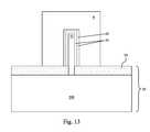
- FIG. 13illustrates a cross-sectional view of a tri-gate FinFET, wherein no gate dielectric is formed
- FIG. 14illustrates a double-gate FinFET comprising three semiconductor materials in the fin.
- FIG. 15illustrates a tri-gate FinFET comprising three semiconductor materials in the fin.
- Novel fin field-effect transistorsand the methods of forming the same are presented.
- the intermediate stages of manufacturing embodiments of the present inventionare illustrated. The variations and the operation of the embodiments are discussed.
- like reference numbersare used to designate like elements.
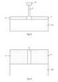
- FIG. 2illustrates a perspective view of FinFET 100 (which may be an n-type FinFET) formed on base material 10 .
- Base material 10may be formed of a dielectric material, for example, silicon oxide.
- base material 10may be formed of a semiconductor material including, but not limited to, silicon, germanium, gallium arsenide, and the like.
- base materials 10may include portions of a semiconductor substrate and isolation structures in the semiconductor substrate.
- FinFET 100includes source region 4 , drain region 6 , and fin 20 therebetween. FinFET 100 may be an NFET, and hence source region 4 and drain region 6 are n-type regions doped with an n-type impurity, for example, by implantations.
- Gate dielectric 12may be formed on the top and opposite sidewalls of fin 20 .
- Gate electrode 8is further formed on gate dielectric 12 . In an embodiment, gate dielectric 12 may be omitted.
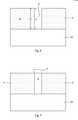
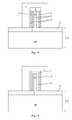
- FIG. 3Aillustrates the cross-sectional view of a double-gate FinFET.
- Fin 20comprises central fin 22 formed of a first semiconductor material.
- Fin 20further comprises semiconductor layer(s) 24 that are formed of a second semiconductor material different from the first semiconductor material.
- Semiconductor layer(s) 24are formed on opposite sidewalls of central fin 22 .
- Gate dielectric 12is formed on sidewalls of semiconductor layer(s) 24 .
- Gate electrode 8is formed on gate dielectric 12 .
- Gate dielectric 12may be formed of commonly used dielectric material such as silicon oxide, silicon nitride, oxynitrides, multi-layers thereof, and combinations thereof. Gate dielectric 12 may also be formed of high-k dielectric materials. The exemplary high-k materials may have k values greater than about 4.0, or even greater than about 7.0, and may include aluminum-containing dielectrics such as Al 2 O 3 , HfAlO, HfAlON, AlZrO, Hf-containing materials such as HfO 2 , HfSiO x , HfAlO x , HfZrSiO x , HfSiON, and other materials such as LaAlO 3 and ZrO 2 . Gate electrode 8 may be formed of doped polysilicon, metals, metal nitrides, metal silicides, and the like.
- FIG. 3Billustrates a schematic band diagram of the double-gate FinFET as shown in FIG. 3A .
- central fin 22has bandgap EgA, while semiconductor layer(s) 24 have bandgap EgB greater than bandgap EgA.
- bandgap EgAis lower than bandgap EgB by about 0.1 eV, although greater or lower bandgap differences may also apply.
- Conduction band EcA of central fin 22may also be lower than conduction band EcB of semiconductor layer(s) 24 .
- conduction band EcAis lower than conduction band EcB by about 0.05 eV, although greater or lower conduction band differences may also apply.
- central fin 22 and semiconductor layer(s) 24may be selected by comparing the bandgaps of the available semiconductor materials with high electron mobilities, which may include, but are not limited to, silicon, germanium, GaAs, InP, GaN, InGaAs, InAlAs, GaSb, AlSb, AlAs, AlP, GaP, and the like.
- central fin 22comprises InGaAs
- semiconductor layer(s) 24comprise GaAs.
- central fin 22comprises InAs
- semiconductor layer(s) 24comprise InAlAs.
- fin 20(including central fin 22 and semiconductor layer(s) 24 ) forms a quantum well.
- gate electrode 8When a non-zero gate voltage is applied to gate electrode 8 , due to the quantum confinement effect, electrons tend to flow through the central portion of fin 20 , that is, central fin 22 . Accordingly, the carrier mobility is high because of the low bandgap EgA, and hence the on-current Ion of the respective FinFET 100 is high.
- FinFET 100when FinFET 100 is turned off with the gate voltage being zero volts, electrons tend to flow through the surface layers of fin 20 , that is, semiconductor layer(s) 24 . Accordingly, the carrier mobility is low due to the high bandgap EgB, and hence the off-current (leakage current) Ioff of the respective FinFET 100 is low. FinFET 100 thus has a high on/off current ratio.
- thickness T 1 of central semiconductor fin 20is preferably small. In an exemplary embodiment, thickness T 1 is less than about 50 nm, and may even be less than about 10 nm. Thickness T 2 of semiconductor layer(s) 24 may be less than about 50 nm.
- FIG. 3Afurther includes hard mask 26 on top of semiconductor fin 20 , wherein hard mask 26 may be formed of commonly used dielectric materials such as silicon nitride, silicon oxide, silicon oxynitride, and the like.
- FinFET 100 as shown in FIG. 3Ais a double-gate FinFET.
- FinFET 100as shown in FIG. 4 is a tri-gate FinFET.
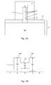
- FIGS. 5 through 8illustrate cross-sectional views of intermediate stages in the manufacturing of the embodiment shown in FIG. 3A .
- substrate 200is provided.
- Substrate 200may be a semiconductor formed of commonly used semiconductor materials such as silicon, germanium, GaAs, or the like.
- Insulation regionssuch as shallow trench isolation (STI) regions 30 are formed in substrate 200 .
- the spacing S between neighboring STI regions 30may be small, for example, less than about 50 nm, which spacing may be equal to or greater than thickness T 1 of central fin 22 as shown in FIG. 3A .
- Recessing depth D 1may be substantially equal to or less than thickness D 2 of STI regions 30 .
- central fin 22is epitaxially grown in recess 32 .
- Hard mask 26may be blanket formed and patterned to cover central fin 22 , as also shown in FIG. 7 .
- substrate 200comprises compound semiconductor materials of group III and group V elements (referred to as III-V compound semiconductors hereinafter), and hence the formation of recess 32 and the epitaxial growth in recess 32 may be omitted. Accordingly, the portion of substrate 200 between STI regions 30 is central fin 22 .
- top portions of STI regions 30are selectively etched, while bottom portions are left un-etched.
- central fin 22has a portion standing above the bottom portions of STI regions 30 .
- an isotropic etchis performed to laterally recess central fin 22 , so that hard mask 26 extends beyond edges of the remaining central fin 22 .
- semiconductor layer(s) 24are epitaxially grown, followed by the formation of gate dielectric layer 12 .
- gate electrode 8is formed, resulting in the structure as shown in FIG. 3A .
- FIGS. 9 through 11illustrate cross-sectional views of intermediate stages in the manufacturing of the embodiment shown in FIG. 4 .
- the initial stepswhich involve the formation of STI regions 30 in substrate 200 and optionally the recessing and epitaxial growth of central fin 22 are essentially the same as shown FIGS. 5-7 .
- no hard maskis formed.
- FIG. 10illustrates the recessing of STI regions 30 , so that central fin 22 has a portion protruding above the remaining portions of STI regions 30 .
- semiconductor layer(s) 24are epitaxially grown, followed by the formation of gate dielectric layer 12 .
- gate electrode 8is formed, resulting in the structure as shown in FIG. 4 .
- FIG. 12Aillustrates yet another double-gate FinFET.
- This embodimentis similar to the embodiment as shown in FIG. 3A , except that no gate dielectric 12 is formed.
- gate electrode 8may be formed of metal, so that a Schottky barrier is formed between gate electrode 8 and semiconductor layer(s) 24 , resulting in depletion layers 40 , which act as gate dielectrics that electrically insulate gate electrode 8 from semiconductor layer(s) 24 .
- a band diagramis illustrated in FIG. 12B .
- the materials of central fin 22 and semiconductor layer(s) 24have been discussed in preceding paragraphs, and hence are not repeated herein. Again, bandgap EgA of central fin 22 may be less than bandgap EgB of semiconductor layer(s) 24 . Also, conduction band EcA of central fin 22 may be less than conduction band EcB of semiconductor layer(s) 24 .
- FIG. 13illustrates yet another tri-gate FinFET embodiment. This embodiment is similar to the embodiment as shown in FIG. 4 , except gate dielectric 12 as shown in FIG. 4 is replaced by depletion region 40 resulting from the Schottky barrier formed between gate electrode 8 and semiconductor layer(s) 24 .
- FIGS. 14 and 15illustrate yet other multiple-gate FinFETs, wherein the quantum wells are formed of more than two semiconductor materials.
- semiconductor layer(s) 44may be formed between semiconductor layer(s) 24 and central fin 22 .
- the bandgap of semiconductor layer(s) 44is higher than bandgap EgA of central fin 22 , and lower than bandgap EgB of semiconductor layer(s) 24 (refer to FIGS. 3B and 13B ).
- the conduction band of semiconductor layer(s) 44may be higher than conduction band EcA of central fin 22 , and lower than conduction band EcB of semiconductor layer(s) 24 (refer to FIGS. 3B and 13B ).
- hard mask 26is formed, while no hard mask is formed in FIG. 15 .
Landscapes
- Insulated Gate Type Field-Effect Transistor (AREA)
- Thin Film Transistor (AREA)
Abstract
Description
- This application claims the benefit of U.S. Provisional Application No. 61/165,803 filed on Apr. 1, 2009, entitled “High-Mobility Multiple-Gate Transistor with Improved On-to-Off Current Ratio,” which application is hereby incorporated herein by reference.
- This invention relates generally to integrated circuit devices, and more particularly to metal-oxide-semiconductor (MOS) transistors and methods for forming the same.
- The speeds of metal-oxide-semiconductor (MOS) transistors are closely related to the drive currents of the MOS transistors, which drive currents are further closely related to the mobility of charges. For example, NMOS transistors have high drive currents when the electron mobility in their channel regions is high, while PMOS transistors have high drive currents when the hole mobility in their channel regions is high.
- Germanium is a commonly known semiconductor material. The electron mobility and hole mobility of germanium are greater than that of silicon, which is the most commonly used semiconductor material in the formation of integrated circuits. Hence, germanium is an excellent material for forming integrated circuits. However, in the past, silicon gained more popularity over germanium since its oxide (silicon oxide) is readily usable in the gate dielectric of MOS transistors. The gate dielectrics of the MOS transistors can be conveniently formed by thermal oxidation of silicon substrates. The oxide of germanium, on the other hand, is soluble in water, and hence is not suitable for the formation of gate dielectrics.
- With the use of high-k dielectric materials in the gate dielectrics of MOS transistors, however, the convenience provided by the silicon oxide is no longer a big advantage, and hence germanium is reexamined for use in integrated circuits.
- In addition to germanium, compound semiconductor materials of group III and group V elements (referred to as III-V compound semiconductors hereinafter) are also good candidates for forming NMOS devices for their high electron mobility.
- A challenge faced by the semiconductor industry is that although the MOS transistors formed on germanium and III-V compound semiconductors have high drive currents, the leakage currents of these MOS transistors are also high. This is partially caused by the low bandgap and the high dielectric constants of germanium and the III-V compound semiconductors. For example,
FIG. 1 illustrates the comparison of bandgaps and dielectric constants of germanium and some commonly used III-V compound semiconductors, and some other semiconductor materials.FIG. 1 reveals that the bandgaps of germanium and some commonly used III-V compound semiconductors are small. Therefore, the respective MOS transistors suffer from band-to-band leakage currents between their gates and source/drain regions. The high dielectric constants of these materials further worsen the leakage currents. As a result, the on/off current ratios (Ion/Ioff) of these MOS transistors are relatively low. - In accordance with one aspect of the present invention, a multi-gate transistor includes a semiconductor fin over a substrate. The semiconductor fin includes a central fin formed of a first semiconductor material; and a semiconductor layer having a first portion and a second portion on opposite sidewalls of the central fin. The semiconductor layer includes a second semiconductor material different from the first semiconductor material. The multi-gate transistor further includes a gate electrode wrapping around sidewalls of the semiconductor fin; and a source region and a drain region on opposite ends of the semiconductor fin. Each of the central fin and the semiconductor layer extends from the source region to the drain region.
- In accordance with another aspect of the present invention, a multi-gate transistor includes a substrate and a semiconductor fin over the substrate. The semiconductor fin includes a central fin formed of a first semiconductor material, and a semiconductor layer including a first portion and a second portion on opposite sidewalls of, and adjoining, the central fin. The central fin and the semiconductor layer form a quantum well. The multi-gate transistor further includes a gate dielectric having a first portion on an outer sidewall of the first portion of the semiconductor layer and a second portion on an outer sidewall of the second portion of the semiconductor layer; a gate electrode over the gate dielectric; and a source region and a drain region on opposite ends of, and adjoining, the central fin and the semiconductor layer. The source region and the drain region are n-type regions.
- In accordance with yet another aspect of the present invention, a method of forming a multi-gate transistor includes forming a semiconductor fin, which further includes forming a central fin including a first semiconductor material; and forming a semiconductor layer including a first portion and a second portion on opposite sidewalls of the central fin. The semiconductor layer includes a second semiconductor material different from the first semiconductor material. The method further includes forming a gate electrode wrapping around sidewalls of the semiconductor fin; and forming a source region and a drain region on opposite ends of the semiconductor fin. Each of the central fin and the semiconductor layer extends from the source region to the drain region.
- In accordance with yet another aspect of the present invention, a method of forming a multi-gate transistor includes providing a semiconductor substrate; forming insulation regions in the semiconductor substrate and adjacent to each other; recessing the insulation regions, so that a region between the insulation regions forms a central fin including a first semiconductor material; epitaxially growing a semiconductor layer including a first portion and a second portion on opposite sidewalls of the central fin, wherein the semiconductor layer includes a second semiconductor material different from the first semiconductor material; forming a gate electrode over a top surface and wrapping around sidewalls of the semiconductor fin; and forming a source region and a drain region on opposite ends of the semiconductor fin. Each of the central fin and the semiconductor layer extends from the source region to the drain region.
- The advantageous features of the present invention include improved performance in MOS transistors including improved drive currents, reduced leakage currents, and high on-to-off current ratios.
- For a more complete understanding of the present invention, and the advantages thereof, reference is now made to the following descriptions taken in conjunction with the accompanying drawings, in which:
FIG. 1 illustrates bandgaps and dielectric constants of some semiconductor materials;FIG. 2 illustrates a perspective view of an embodiment;FIG. 3A illustrates a cross-sectional view of a double-gate fin field-effect transistor (FinFET);FIG. 3B illustrates a band diagram of the embodiment shown inFIG. 3A ;FIG. 4 illustrates a cross-sectional view of a tri-gate FinFET;FIGS. 5 through 8 are cross-sectional views of intermediate stages in the manufacturing of the double-gate FinFET as shown inFIG. 3A ;FIGS. 9 through 11 are cross-sectional views of intermediate stages in the manufacturing of the tri-gate FinFET as shown inFIG. 4 ;FIG. 12A illustrates a cross-sectional view of a double-gate FinFET, wherein no gate dielectric is formed;FIG. 12B illustrates a band diagram of the embodiment shown inFIG. 12A ;FIG. 13 illustrates a cross-sectional view of a tri-gate FinFET, wherein no gate dielectric is formed;FIG. 14 illustrates a double-gate FinFET comprising three semiconductor materials in the fin; andFIG. 15 illustrates a tri-gate FinFET comprising three semiconductor materials in the fin.- The making and using of the embodiments of the present invention are discussed in detail below. It should be appreciated, however, that the embodiments provide many applicable inventive concepts that can be embodied in a wide variety of specific contexts. The specific embodiments discussed are merely illustrative of specific ways to make and use the invention, and do not limit the scope of the invention.
- Novel fin field-effect transistors (FinFETs) and the methods of forming the same are presented. The intermediate stages of manufacturing embodiments of the present invention are illustrated. The variations and the operation of the embodiments are discussed. Throughout the various views and illustrative embodiments of the present invention, like reference numbers are used to designate like elements.
FIG. 2 illustrates a perspective view of FinFET100 (which may be an n-type FinFET) formed onbase material 10.Base material 10 may be formed of a dielectric material, for example, silicon oxide. Alternatively,base material 10 may be formed of a semiconductor material including, but not limited to, silicon, germanium, gallium arsenide, and the like. In yet other embodiments,base materials 10 may include portions of a semiconductor substrate and isolation structures in the semiconductor substrate.FinFET 100 includessource region 4, drainregion 6, andfin 20 therebetween.FinFET 100 may be an NFET, and hence sourceregion 4 and drainregion 6 are n-type regions doped with an n-type impurity, for example, by implantations.Gate dielectric 12 may be formed on the top and opposite sidewalls offin 20.Gate electrode 8 is further formed ongate dielectric 12. In an embodiment,gate dielectric 12 may be omitted.- The cross-sectional views that are shown in detail in subsequent paragraphs, unless specified otherwise, are made across a vertical
plane crossing line 3A-3A inFIG. 2 .FIG. 3A illustrates the cross-sectional view of a double-gate FinFET.Fin 20 comprisescentral fin 22 formed of a first semiconductor material.Fin 20 further comprises semiconductor layer(s)24 that are formed of a second semiconductor material different from the first semiconductor material. Semiconductor layer(s)24 are formed on opposite sidewalls ofcentral fin 22.Gate dielectric 12 is formed on sidewalls of semiconductor layer(s)24.Gate electrode 8 is formed ongate dielectric 12. Gate dielectric 12 may be formed of commonly used dielectric material such as silicon oxide, silicon nitride, oxynitrides, multi-layers thereof, and combinations thereof.Gate dielectric 12 may also be formed of high-k dielectric materials. The exemplary high-k materials may have k values greater than about 4.0, or even greater than about 7.0, and may include aluminum-containing dielectrics such as Al2O3, HfAlO, HfAlON, AlZrO, Hf-containing materials such as HfO2, HfSiOx, HfAlOx, HfZrSiOx, HfSiON, and other materials such as LaAlO3and ZrO2.Gate electrode 8 may be formed of doped polysilicon, metals, metal nitrides, metal silicides, and the like.FIG. 3B illustrates a schematic band diagram of the double-gate FinFET as shown inFIG. 3A . In an embodiment,central fin 22 has bandgap EgA, while semiconductor layer(s)24 have bandgap EgB greater than bandgap EgA. In an exemplary embodiment, bandgap EgA is lower than bandgap EgB by about 0.1 eV, although greater or lower bandgap differences may also apply. Conduction band EcA ofcentral fin 22 may also be lower than conduction band EcB of semiconductor layer(s)24. In an exemplary embodiment, conduction band EcA is lower than conduction band EcB by about 0.05 eV, although greater or lower conduction band differences may also apply. The appropriate materials ofcentral fin 22 and semiconductor layer(s)24 may be selected by comparing the bandgaps of the available semiconductor materials with high electron mobilities, which may include, but are not limited to, silicon, germanium, GaAs, InP, GaN, InGaAs, InAlAs, GaSb, AlSb, AlAs, AlP, GaP, and the like. In an exemplary embodiment,central fin 22 comprises InGaAs, while semiconductor layer(s)24 comprise GaAs. In other embodiments,central fin 22 comprises InAs, while semiconductor layer(s)24 comprise InAlAs.- Referring back to
FIG. 3A , with bandgap EgA ofcentral fin 22 being lower than bandgap EgB of semiconductor layer(s)24, fin20 (includingcentral fin 22 and semiconductor layer(s)24) forms a quantum well. When a non-zero gate voltage is applied togate electrode 8, due to the quantum confinement effect, electrons tend to flow through the central portion offin 20, that is,central fin 22. Accordingly, the carrier mobility is high because of the low bandgap EgA, and hence the on-current Ion of therespective FinFET 100 is high. On the other hand, whenFinFET 100 is turned off with the gate voltage being zero volts, electrons tend to flow through the surface layers offin 20, that is, semiconductor layer(s)24. Accordingly, the carrier mobility is low due to the high bandgap EgB, and hence the off-current (leakage current) Ioff of therespective FinFET 100 is low.FinFET 100 thus has a high on/off current ratio. - To improve the performance of
FinFET 100, the quantum well needs to be strengthened. Accordingly, thickness T1 ofcentral semiconductor fin 20 is preferably small. In an exemplary embodiment, thickness T1 is less than about 50 nm, and may even be less than about 10 nm. Thickness T2 of semiconductor layer(s)24 may be less than about 50 nm. FIG. 3A further includeshard mask 26 on top ofsemiconductor fin 20, whereinhard mask 26 may be formed of commonly used dielectric materials such as silicon nitride, silicon oxide, silicon oxynitride, and the like.FinFET 100 as shown inFIG. 3A is a double-gate FinFET.- In alternative embodiments, as shown in
FIG. 4 , no hard mask is formed on top offin 20. Instead, semiconductor layer(s)24 on opposite sidewalls ofcentral fin 22 are joined by a portion on top ofcentral fin 22 to form a continuous layer.Gate dielectric 12 also forms a continuous layer.FinFET 100 as shown inFIG. 4 is a tri-gate FinFET. FIGS. 5 through 8 illustrate cross-sectional views of intermediate stages in the manufacturing of the embodiment shown inFIG. 3A . Referring toFIG. 5 ,substrate 200 is provided.Substrate 200 may be a semiconductor formed of commonly used semiconductor materials such as silicon, germanium, GaAs, or the like. Insulation regions such as shallow trench isolation (STI)regions 30 are formed insubstrate 200. The spacing S between neighboringSTI regions 30 may be small, for example, less than about 50 nm, which spacing may be equal to or greater than thickness T1 ofcentral fin 22 as shown inFIG. 3A .- Next, as shown in
FIG. 6 , the portion ofsubstrate 200 between opposingSTI regions 30 is recessed to formrecess 32. Recessing depth D1 may be substantially equal to or less than thickness D2 ofSTI regions 30. InFIG. 7 ,central fin 22 is epitaxially grown inrecess 32.Hard mask 26 may be blanket formed and patterned to covercentral fin 22, as also shown inFIG. 7 . - In alternative embodiments,
substrate 200 comprises compound semiconductor materials of group III and group V elements (referred to as III-V compound semiconductors hereinafter), and hence the formation ofrecess 32 and the epitaxial growth inrecess 32 may be omitted. Accordingly, the portion ofsubstrate 200 betweenSTI regions 30 iscentral fin 22. - Next, as shown in
FIG. 8 , top portions ofSTI regions 30 are selectively etched, while bottom portions are left un-etched. As a result,central fin 22 has a portion standing above the bottom portions ofSTI regions 30. After the formation ofhard mask 26, an isotropic etch is performed to laterally recesscentral fin 22, so thathard mask 26 extends beyond edges of the remainingcentral fin 22. Next, as shown inFIG. 3A , semiconductor layer(s)24 are epitaxially grown, followed by the formation ofgate dielectric layer 12. In subsequent steps,gate electrode 8 is formed, resulting in the structure as shown inFIG. 3A . FIGS. 9 through 11 illustrate cross-sectional views of intermediate stages in the manufacturing of the embodiment shown inFIG. 4 . The initial steps, which involve the formation ofSTI regions 30 insubstrate 200 and optionally the recessing and epitaxial growth ofcentral fin 22 are essentially the same as shownFIGS. 5-7 . However, as shown inFIG. 9 , no hard mask is formed.FIG. 10 illustrates the recessing ofSTI regions 30, so thatcentral fin 22 has a portion protruding above the remaining portions ofSTI regions 30. Next, as shown inFIG. 11 , semiconductor layer(s)24 are epitaxially grown, followed by the formation ofgate dielectric layer 12. In subsequent steps,gate electrode 8 is formed, resulting in the structure as shown inFIG. 4 .FIG. 12A illustrates yet another double-gate FinFET. This embodiment is similar to the embodiment as shown inFIG. 3A , except that nogate dielectric 12 is formed. In this embodiment,gate electrode 8 may be formed of metal, so that a Schottky barrier is formed betweengate electrode 8 and semiconductor layer(s)24, resulting indepletion layers 40, which act as gate dielectrics that electrically insulategate electrode 8 from semiconductor layer(s)24. A band diagram is illustrated inFIG. 12B . The materials ofcentral fin 22 and semiconductor layer(s)24 have been discussed in preceding paragraphs, and hence are not repeated herein. Again, bandgap EgA ofcentral fin 22 may be less than bandgap EgB of semiconductor layer(s)24. Also, conduction band EcA ofcentral fin 22 may be less than conduction band EcB of semiconductor layer(s)24.FIG. 13 illustrates yet another tri-gate FinFET embodiment. This embodiment is similar to the embodiment as shown inFIG. 4 , exceptgate dielectric 12 as shown inFIG. 4 is replaced bydepletion region 40 resulting from the Schottky barrier formed betweengate electrode 8 and semiconductor layer(s)24.FIGS. 14 and 15 illustrate yet other multiple-gate FinFETs, wherein the quantum wells are formed of more than two semiconductor materials. For example, semiconductor layer(s)44 may be formed between semiconductor layer(s)24 andcentral fin 22. In an embodiment, the bandgap of semiconductor layer(s)44 is higher than bandgap EgA ofcentral fin 22, and lower than bandgap EgB of semiconductor layer(s)24 (refer toFIGS. 3B and 13B ). Also, the conduction band of semiconductor layer(s)44 may be higher than conduction band EcA ofcentral fin 22, and lower than conduction band EcB of semiconductor layer(s)24 (refer toFIGS. 3B and 13B ). InFIG. 14 ,hard mask 26 is formed, while no hard mask is formed inFIG. 15 .- Although the present invention and its advantages have been described in detail, it should be understood that various changes, substitutions and alterations can be made herein without departing from the spirit and scope of the invention as defined by the appended claims. Moreover, the scope of the present application is not intended to be limited to the particular embodiments of the process, machine, manufacture, and composition of matter, means, methods and steps described in the specification. As one of ordinary skill in the art will readily appreciate from the disclosure of the present invention, processes, machines, manufacture, compositions of matter, means, methods, or steps, presently existing or later to be developed, that perform substantially the same function or achieve substantially the same result as the corresponding embodiments described herein may be utilized according to the present invention. Accordingly, the appended claims are intended to include within their scope such processes, machines, manufacture, compositions of matter, means, methods, or steps. In addition, each claim constitutes a separate embodiment, and the combination of various claims and embodiments are within the scope of the invention.
Claims (20)
1. A multi-gate transistor comprising:
a substrate;
a semiconductor fin over the substrate and comprising:
a central fin formed of a first semiconductor material; and
a semiconductor layer comprising a first portion and a second portion on opposite sidewalls of the central fin, wherein the semiconductor layer comprises a second semiconductor material different from the first semiconductor material;
a gate electrode wrapping around sidewalls of the semiconductor fin; and
a source region and a drain region on opposite ends of the semiconductor fin, wherein each of the central fin and the semiconductor layer extends from the source region to the drain region.
2. The multi-gate transistor ofclaim 1 , wherein the central fin and the semiconductor layer form a quantum well.
3. The multi-gate transistor ofclaim 1 , wherein the first semiconductor material has a bandgap lower than a bandgap of the second semiconductor material.
4. The multi-gate transistor ofclaim 1 , wherein the first semiconductor material has a conduction band lower than a conduction band of the second semiconductor material.
5. The multi-gate transistor ofclaim 1 , wherein the source region and the drain region are n-type regions.
6. The multi-gate transistor ofclaim 1 further comprising a gate dielectric comprising a first portion on an outer sidewall of the first portion of the semiconductor layer, and a second portion on an outer sidewall of the second portion of the semiconductor layer.
7. The multi-gate transistor ofclaim 1 , wherein the gate electrode contacts the first portion and the second portion of the semiconductor layer.
8. The multi-gate transistor ofclaim 1 , wherein the semiconductor layer further comprises a third portion on a top surface of the central fin and connecting the first portion of the semiconductor layer to the second portion of the semiconductor layer.
9. The multi-gate transistor ofclaim 1 further comprising a hard mask on a top surface of the central fin and disconnecting the first portion of the semiconductor layer from the second portion of the semiconductor layer.
10. The multi-gate transistor ofclaim 9 , wherein the hard mask extends directly over the first portion and the second portion of the semiconductor layer.
11. The multi-gate transistor ofclaim 1 further comprising an additional semiconductor layer comprising:
a first portion between the first portion of the semiconductor layer and the central fin; and
a second portion between the second portion of the semiconductor layer and the central fin, wherein the additional semiconductor layer has a bandgap greater than a bandgap of the central fin, and lower than a bandgap of the semiconductor layer.
12. A multi-gate transistor comprising:
a substrate;
a semiconductor fin over the substrate and comprising:
a central fin formed of a first semiconductor material; and
a semiconductor layer comprising a first portion and a second portion on opposite sidewalls of, and adjoining, the central fin, wherein the semiconductor layer comprises a second semiconductor material different from the first semiconductor material, and wherein the central fin and the semiconductor layer form a quantum well;
a gate dielectric comprising a first portion on an outer sidewall of the first portion of the semiconductor layer, and a second portion on an outer sidewall of the second portion of the semiconductor layer;
a gate electrode over the gate dielectric; and
a source region and a drain region on opposite ends of, and adjoining, the central fin and the semiconductor layer, wherein the source region and the drain region are n-type regions.
13. The multi-gate transistor ofclaim 12 , wherein the central fin extends down into the substrate, and wherein the substrate comprises an insulation region, with the insulation region having an end contacting a sidewall of the central fin, and a top surface contacting a bottom end of the semiconductor layer.
14. The multi-gate transistor ofclaim 12 , wherein the first semiconductor material has a bandgap lower than a bandgap of the second semiconductor material.
15. The multi-gate transistor ofclaim 14 , wherein the first bandgap is lower than the second bandgap by greater than about 0.1 eV.
16. The multi-gate transistor ofclaim 12 , wherein the first semiconductor material has a first conduction band lower than a second conduction band of the second semiconductor material.
17. The multi-gate transistor ofclaim 12 , wherein the central fin has a thickness less than about 10 nm.
18. The multi-gate transistor ofclaim 12 , wherein the semiconductor layer further comprises a third portion on a top surface of the central fin and connecting the first portion of the semiconductor layer to the second portion of the semiconductor layer.
19. The multi-gate transistor ofclaim 12 further comprising a hard mask on a top surface of the central fin and disconnecting the first portion of the semiconductor layer from the second portion of the semiconductor layer.
20. The multi-gate transistor ofclaim 12 , wherein at least one of the central fin and the semiconductor material comprises a compound semiconductor material comprising a group III element and a group V element.
Priority Applications (7)
| Application Number | Priority Date | Filing Date | Title |
|---|---|---|---|
| US12/639,653US8674341B2 (en) | 2009-04-01 | 2009-12-16 | High-mobility multiple-gate transistor with improved on-to-off current ratio |
| KR1020100028059AKR101145959B1 (en) | 2009-04-01 | 2010-03-29 | High-Mobility Multiple-Gate Transistor with Improved On-to-Off Current Ratio |
| TW099110083ATWI416730B (en) | 2009-04-01 | 2010-04-01 | Multi-gate transistor |
| JP2010085075AJP5452322B2 (en) | 2009-04-01 | 2010-04-01 | High mobility multi-gate transistor with improved on / off current ratio |
| US14/157,638US8927371B2 (en) | 2009-04-01 | 2014-01-17 | High-mobility multiple-gate transistor with improved on-to-off current ratio |
| US14/546,031US9590068B2 (en) | 2009-04-01 | 2014-11-18 | High-mobility multiple-gate transistor with improved on-to-off current ratio |
| US15/443,261US10109748B2 (en) | 2009-04-01 | 2017-02-27 | High-mobility multiple-gate transistor with improved on-to-off current ratio |
Applications Claiming Priority (2)
| Application Number | Priority Date | Filing Date | Title |
|---|---|---|---|
| US16580309P | 2009-04-01 | 2009-04-01 | |
| US12/639,653US8674341B2 (en) | 2009-04-01 | 2009-12-16 | High-mobility multiple-gate transistor with improved on-to-off current ratio |
Related Child Applications (1)
| Application Number | Title | Priority Date | Filing Date |
|---|---|---|---|
| US14/157,638ContinuationUS8927371B2 (en) | 2009-04-01 | 2014-01-17 | High-mobility multiple-gate transistor with improved on-to-off current ratio |
Publications (2)
| Publication Number | Publication Date |
|---|---|
| US20100252816A1true US20100252816A1 (en) | 2010-10-07 |
| US8674341B2 US8674341B2 (en) | 2014-03-18 |
Family
ID=42805239
Family Applications (4)
| Application Number | Title | Priority Date | Filing Date |
|---|---|---|---|
| US12/639,653Active2032-10-16US8674341B2 (en) | 2009-04-01 | 2009-12-16 | High-mobility multiple-gate transistor with improved on-to-off current ratio |
| US14/157,638ActiveUS8927371B2 (en) | 2009-04-01 | 2014-01-17 | High-mobility multiple-gate transistor with improved on-to-off current ratio |
| US14/546,031Active2030-02-26US9590068B2 (en) | 2009-04-01 | 2014-11-18 | High-mobility multiple-gate transistor with improved on-to-off current ratio |
| US15/443,261ActiveUS10109748B2 (en) | 2009-04-01 | 2017-02-27 | High-mobility multiple-gate transistor with improved on-to-off current ratio |
Family Applications After (3)
| Application Number | Title | Priority Date | Filing Date |
|---|---|---|---|
| US14/157,638ActiveUS8927371B2 (en) | 2009-04-01 | 2014-01-17 | High-mobility multiple-gate transistor with improved on-to-off current ratio |
| US14/546,031Active2030-02-26US9590068B2 (en) | 2009-04-01 | 2014-11-18 | High-mobility multiple-gate transistor with improved on-to-off current ratio |
| US15/443,261ActiveUS10109748B2 (en) | 2009-04-01 | 2017-02-27 | High-mobility multiple-gate transistor with improved on-to-off current ratio |
Country Status (5)
| Country | Link |
|---|---|
| US (4) | US8674341B2 (en) |
| JP (1) | JP5452322B2 (en) |
| KR (1) | KR101145959B1 (en) |
| CN (1) | CN101853882B (en) |
| TW (1) | TWI416730B (en) |
Cited By (44)
| Publication number | Priority date | Publication date | Assignee | Title |
|---|---|---|---|---|
| US20090321835A1 (en)* | 2008-06-30 | 2009-12-31 | Frank Wirbeleit | Three-dimensional transistor with double channel configuration |
| US20100301390A1 (en)* | 2009-05-29 | 2010-12-02 | Chih-Hsin Ko | Gradient Ternary or Quaternary Multiple-Gate Transistor |
| US20100301392A1 (en)* | 2009-06-01 | 2010-12-02 | Chih-Hsin Ko | Source/Drain Re-Growth for Manufacturing III-V Based Transistors |
| US20130011983A1 (en)* | 2011-07-07 | 2013-01-10 | Taiwan Semiconductor Manufacturing Company, Ltd. | In-Situ Doping of Arsenic for Source and Drain Epitaxy |
| JP2013513973A (en)* | 2009-12-30 | 2013-04-22 | インテル・コーポレーション | Multi-gate III-V quantum well structure |
| US8455929B2 (en) | 2010-06-30 | 2013-06-04 | Taiwan Semiconductor Manufacturing Company, Ltd. | Formation of III-V based devices on semiconductor substrates |
| US8455860B2 (en) | 2009-04-30 | 2013-06-04 | Taiwan Semiconductor Manufacturing Company, Ltd. | Reducing source/drain resistance of III-V based transistors |
| CN103187272A (en)* | 2013-02-28 | 2013-07-03 | 溧阳市宏达电机有限公司 | Manufacturing method of fin-shaped PIN diode |
| US20130256759A1 (en)* | 2012-03-27 | 2013-10-03 | Taiwan Semiconductor Manufacturing Company, Ltd. | Fin Structure for a FinFET Device |
| US8674341B2 (en) | 2009-04-01 | 2014-03-18 | Taiwan Semiconductor Manufacturing Company, Ltd. | High-mobility multiple-gate transistor with improved on-to-off current ratio |
| US20140084299A1 (en)* | 2012-09-21 | 2014-03-27 | Robert Bosch Gmbh | Vertical microelectronic component and corresponding production method |
| US20140183660A1 (en)* | 2012-12-31 | 2014-07-03 | Chewn-Pu Jou | Power cell and power cell circuit for a power amplifier |
| CN103915336A (en)* | 2013-01-08 | 2014-07-09 | 中芯国际集成电路制造(上海)有限公司 | Three-dimensional quantum well transistor and forming method thereof |
| US8785285B2 (en) | 2012-03-08 | 2014-07-22 | Taiwan Semiconductor Manufacturing Company, Ltd. | Semiconductor devices and methods of manufacture thereof |
| US8816391B2 (en) | 2009-04-01 | 2014-08-26 | Taiwan Semiconductor Manufacturing Company, Ltd. | Source/drain engineering of devices with high-mobility channels |
| US20150077086A1 (en)* | 2013-09-18 | 2015-03-19 | Globalfoundries Inc | Fin width measurement using quantum well structure |
| EP2887399A1 (en)* | 2013-12-20 | 2015-06-24 | Imec | A method for manufacturing a transistor device and associated device |
| US9087902B2 (en) | 2013-02-27 | 2015-07-21 | Taiwan Semiconductor Manufacturing Company, Ltd. | FinFETs with strained well regions |
| US20150221676A1 (en)* | 2014-02-04 | 2015-08-06 | International Business Machines Corporation | FinFET DEVICE CONTAINING A COMPOSITE SPACER STRUCTURE |
| US20150279936A1 (en)* | 2012-02-02 | 2015-10-01 | International Business Machines Corporation | Strained channel for depleted channel semiconductor devices |
| US9159824B2 (en)* | 2013-02-27 | 2015-10-13 | Taiwan Semiconductor Manufacturing Company, Ltd. | FinFETs with strained well regions |
| US20150294879A1 (en)* | 2012-11-30 | 2015-10-15 | Institute of Microelectronics, Chinese Academy of Sciences | Method for manufacturing fin structure |
| US20150340294A1 (en)* | 2014-05-21 | 2015-11-26 | International Business Machines Corporation | Structure and method for effective device width adjustment in finfet devices using gate workfunction shift |
| US20150380438A1 (en)* | 2014-06-26 | 2015-12-31 | International Business Machines Corporation | Trapping dislocations in high-mobility fins below isolation layer |
| US9236483B2 (en) | 2014-02-12 | 2016-01-12 | Qualcomm Incorporated | FinFET with backgate, without punchthrough, and with reduced fin height variation |
| US20160163843A1 (en)* | 2014-06-06 | 2016-06-09 | Taiwan Semiconductor Manufacturing Company, Ltd. | Quantum Well Fin-Like Field Effect Transistor (QWFINFET) Having a Two-Section Combo QW Structure |
| US20160172477A1 (en)* | 2013-09-27 | 2016-06-16 | Intel Corporation | Methods to achieve high mobility in cladded iii-v channel materials |
| US9385234B2 (en) | 2013-02-27 | 2016-07-05 | Taiwan Semiconductor Manufacturing Company, Ltd. | FinFETs with strained well regions |
| KR20160101900A (en)* | 2013-12-23 | 2016-08-26 | 인텔 코포레이션 | Pre-sculpting of si fin elements prior to cladding for transistor channel applications |
| GB2524411B (en)* | 2012-12-19 | 2017-02-15 | Intel Corp | Group III-N transistors on nanoscale template structures |
| US9608117B2 (en) | 2015-03-30 | 2017-03-28 | Samsung Electronics Co., Ltd. | Semiconductor devices including a finFET |
| EP3050092A4 (en)* | 2013-09-27 | 2017-05-03 | Intel Corporation | Non-silicon device heterolayers on patterned silicon substrate for cmos by combination of selective and conformal epitaxy |
| US20170162387A1 (en)* | 2015-12-04 | 2017-06-08 | International Business Machines Corporation | Integration of iii-v compound materials on silicon |
| US9735239B2 (en) | 2012-04-11 | 2017-08-15 | Taiwan Semiconductor Manufacturing Company, Ltd. | Semiconductor device channel system and method |
| US20170236841A1 (en)* | 2016-02-11 | 2017-08-17 | Qualcomm Incorporated | Fin with an epitaxial cladding layer |
| EP3123519A4 (en)* | 2014-03-24 | 2017-10-25 | Intel Corporation | Fin sculpting and cladding during replacement gate process for transistor channel applications |
| US9853026B2 (en)* | 2013-06-04 | 2017-12-26 | Semiconductor Manufacturing International (Shanghai) Corporation | FinFET device and fabrication method thereof |
| WO2018095931A3 (en)* | 2016-11-24 | 2018-08-02 | Cambridge Enterprise Limited | A gallium nitride transistor |
| US20190207028A1 (en)* | 2018-01-03 | 2019-07-04 | International Business Machines Corporation | Transistor having an oxide-isolated strained channel fin on a bulk substrate |
| US10854752B2 (en) | 2014-03-27 | 2020-12-01 | Intel Corporation | High mobility strained channels for fin-based NMOS transistors |
| US20220384431A1 (en)* | 2021-05-28 | 2022-12-01 | Fujian Jinhua Integrated Circuit Co., Ltd. | Semiconductor device and method of forming the same |
| US20230091260A1 (en)* | 2021-09-23 | 2023-03-23 | Texas Instruments Incorporated | LOW RESISTIVE SOURCE/BACKGATE finFET |
| WO2023245756A1 (en)* | 2022-06-23 | 2023-12-28 | 长鑫存储技术有限公司 | Semiconductor structure and method for forming same |
| US12426237B2 (en) | 2022-06-23 | 2025-09-23 | Changxin Memory Technologies, Inc. | Semiconductor structure and method for forming same |
Families Citing this family (35)
| Publication number | Priority date | Publication date | Assignee | Title |
|---|---|---|---|---|
| US8283653B2 (en) | 2009-12-23 | 2012-10-09 | Intel Corporation | Non-planar germanium quantum well devices |
| KR101160084B1 (en)* | 2011-02-01 | 2012-06-26 | 서울대학교산학협력단 | Semiconductor memory device having low leakage current |
| US8890207B2 (en)* | 2011-09-06 | 2014-11-18 | Taiwan Semiconductor Manufacturing Company, Ltd. | FinFET design controlling channel thickness |
| KR101700213B1 (en)* | 2011-12-21 | 2017-01-26 | 인텔 코포레이션 | Methods for forming fins for metal oxide semiconductor device structures |
| KR101823105B1 (en)* | 2012-03-19 | 2018-01-30 | 삼성전자주식회사 | Method for fabricating field effect transistor |
| US9748338B2 (en) | 2012-06-29 | 2017-08-29 | Intel Corporation | Preventing isolation leakage in III-V devices |
| TWI553858B (en)* | 2012-07-11 | 2016-10-11 | 聯華電子股份有限公司 | Multi-gate mosfet and process thereof |
| TWI644433B (en)* | 2013-03-13 | 2018-12-11 | 半導體能源研究所股份有限公司 | Semiconductor device |
| TWI620324B (en)* | 2013-04-12 | 2018-04-01 | 半導體能源研究所股份有限公司 | Semiconductor device |
| CN104217948B (en)* | 2013-05-31 | 2018-04-03 | 中国科学院微电子研究所 | Semiconductor manufacturing method |
| CN104253044B (en)* | 2013-06-26 | 2017-03-29 | 中芯国际集成电路制造(上海)有限公司 | Transistor and forming method thereof |
| CN105531797A (en)* | 2013-06-28 | 2016-04-27 | 英特尔公司 | Nanostructures and nanofeatures with Si(111) planes on Si(100) wafers for III-N epitaxy |
| CN104347408B (en)* | 2013-07-31 | 2017-12-26 | 中芯国际集成电路制造(上海)有限公司 | Semiconductor device and its manufacture method |
| CN104347407B (en)* | 2013-07-31 | 2017-10-31 | 中芯国际集成电路制造(上海)有限公司 | Semiconductor device and its manufacture method |
| US9583590B2 (en) | 2013-09-27 | 2017-02-28 | Samsung Electronics Co., Ltd. | Integrated circuit devices including FinFETs and methods of forming the same |
| CN105493251A (en)* | 2013-09-27 | 2016-04-13 | 英特尔公司 | Non-planar semiconductor device with multi-layer flexible substrate |
| US9178045B2 (en)* | 2013-09-27 | 2015-11-03 | Samsung Electronics Co., Ltd. | Integrated circuit devices including FinFETS and methods of forming the same |
| JP6438727B2 (en)* | 2013-10-11 | 2018-12-19 | 株式会社半導体エネルギー研究所 | Semiconductor device and manufacturing method of semiconductor device |
| CN104576385A (en)* | 2013-10-14 | 2015-04-29 | 中国科学院微电子研究所 | FinFET structure and manufacturing method thereof |
| US9048303B1 (en)* | 2014-01-30 | 2015-06-02 | Infineon Technologies Austria Ag | Group III-nitride-based enhancement mode transistor |
| US9337279B2 (en) | 2014-03-03 | 2016-05-10 | Infineon Technologies Austria Ag | Group III-nitride-based enhancement mode transistor |
| US9263555B2 (en)* | 2014-07-03 | 2016-02-16 | Globalfoundries Inc. | Methods of forming a channel region for a semiconductor device by performing a triple cladding process |
| US9461179B2 (en)* | 2014-07-11 | 2016-10-04 | Semiconductor Energy Laboratory Co., Ltd. | Thin film transistor device (TFT) comprising stacked oxide semiconductor layers and having a surrounded channel structure |
| KR101611337B1 (en)* | 2014-11-14 | 2016-04-12 | 울산과학기술원 | Method of high-performance and low-power field-effect transistor fabrication without or minimizing surface roughness scattering |
| US9741811B2 (en) | 2014-12-15 | 2017-08-22 | Samsung Electronics Co., Ltd. | Integrated circuit devices including source/drain extension regions and methods of forming the same |
| KR101668442B1 (en)* | 2015-02-17 | 2016-10-21 | 경북대학교 산학협력단 | Manufacturing method for semiconductor device |
| US10833175B2 (en)* | 2015-06-04 | 2020-11-10 | International Business Machines Corporation | Formation of dislocation-free SiGe finFET using porous silicon |
| CN107667430B (en) | 2015-06-26 | 2022-07-22 | 英特尔公司 | High mobility semiconductor source/drain spacers |
| WO2017052608A1 (en) | 2015-09-25 | 2017-03-30 | Intel Corporation | High-electron-mobility transistors with counter-doped dopant diffusion barrier |
| WO2017052619A1 (en) | 2015-09-25 | 2017-03-30 | Intel Corporation | High mobility field effect transistors with a retrograded semiconductor source/drain |
| US10446685B2 (en) | 2015-09-25 | 2019-10-15 | Intel Corporation | High-electron-mobility transistors with heterojunction dopant diffusion barrier |
| US10411007B2 (en) | 2015-09-25 | 2019-09-10 | Intel Corporation | High mobility field effect transistors with a band-offset semiconductor source/drain spacer |
| US10957769B2 (en) | 2016-06-17 | 2021-03-23 | Intel Corporation | High-mobility field effect transistors with wide bandgap fin cladding |
| US9978872B1 (en) | 2017-03-23 | 2018-05-22 | International Business Machines Corporation | Non-polar, III-nitride semiconductor fin field-effect transistor |
| EP3676873A4 (en)* | 2017-08-29 | 2021-05-26 | Micron Technology, Inc. | DEVICES AND SYSTEMS INCLUDING STRING DRIVERS WITH HIGH GAP MATERIAL AND METHODS OF FORMING |
Citations (58)
| Publication number | Priority date | Publication date | Assignee | Title |
|---|---|---|---|---|
| US5621227A (en)* | 1995-07-18 | 1997-04-15 | Discovery Semiconductors, Inc. | Method and apparatus for monolithic optoelectronic integrated circuit using selective epitaxy |
| US6121153A (en)* | 1994-08-29 | 2000-09-19 | Fujitsu Limited | Semiconductor device having a regrowth crystal region |
| US6218685B1 (en)* | 1998-01-08 | 2001-04-17 | Matsushita Electronics Corporation | Semiconductor device and method for fabricating the same |
| US6399970B2 (en)* | 1996-09-17 | 2002-06-04 | Matsushita Electric Industrial Co., Ltd. | FET having a Si/SiGeC heterojunction channel |
| US6475890B1 (en)* | 2001-02-12 | 2002-11-05 | Advanced Micro Devices, Inc. | Fabrication of a field effect transistor with an upside down T-shaped semiconductor pillar in SOI technology |
| US6475869B1 (en)* | 2001-02-26 | 2002-11-05 | Advanced Micro Devices, Inc. | Method of forming a double gate transistor having an epitaxial silicon/germanium channel region |
| US6512252B1 (en)* | 1999-11-15 | 2003-01-28 | Matsushita Electric Industrial Co., Ltd. | Semiconductor device |
| US20030178677A1 (en)* | 2002-03-19 | 2003-09-25 | International Business Machines Corporation | Strained fin fets structure and method |
| US6706571B1 (en)* | 2002-10-22 | 2004-03-16 | Advanced Micro Devices, Inc. | Method for forming multiple structures in a semiconductor device |
| US6762483B1 (en)* | 2003-01-23 | 2004-07-13 | Advanced Micro Devices, Inc. | Narrow fin FinFET |
| US20040173812A1 (en)* | 2003-03-07 | 2004-09-09 | Amberwave Systems Corporation | Shallow trench isolation process |
| US20040251479A1 (en)* | 2003-06-16 | 2004-12-16 | Matsushita Electric Industrial Co., Ltd. | Semiconductor device and method for fabricating the same |
| US20040256647A1 (en)* | 2003-06-23 | 2004-12-23 | Sharp Laboratories Of America Inc. | Strained silicon finFET device |
| US6858478B2 (en)* | 2002-08-23 | 2005-02-22 | Intel Corporation | Tri-gate devices and methods of fabrication |
| US20050093154A1 (en)* | 2003-07-25 | 2005-05-05 | Interuniversitair Microelektronica Centrum (Imec Vzw) | Multiple gate semiconductor device and method for forming same |
| US20050104137A1 (en)* | 2002-08-12 | 2005-05-19 | Carl Faulkner | Insulated gate field-effect transistor having III-VI source/drain layer(s) |
| US20050153490A1 (en)* | 2003-12-16 | 2005-07-14 | Jae-Man Yoon | Method of forming fin field effect transistor |
| US20050186742A1 (en)* | 2004-02-24 | 2005-08-25 | Chang-Woo Oh | Vertical channel fin field-effect transistors having increased source/drain contact area and methods for fabricating the same |
| US20060057856A1 (en)* | 2004-09-09 | 2006-03-16 | Toshiba Ceramics Co., Ltd. | Manufacturing method for strained silicon wafer |
| US20060076625A1 (en)* | 2004-09-25 | 2006-04-13 | Lee Sung-Young | Field effect transistors having a strained silicon channel and methods of fabricating same |
| US7042009B2 (en)* | 2004-06-30 | 2006-05-09 | Intel Corporation | High mobility tri-gate devices and methods of fabrication |
| US20060148182A1 (en)* | 2005-01-03 | 2006-07-06 | Suman Datta | Quantum well transistor using high dielectric constant dielectric layer |
| US20060292719A1 (en)* | 2005-05-17 | 2006-12-28 | Amberwave Systems Corporation | Lattice-mismatched semiconductor structures with reduced dislocation defect densities and related methods for device fabrication |
| US7190050B2 (en)* | 2005-07-01 | 2007-03-13 | Synopsys, Inc. | Integrated circuit on corrugated substrate |
| US20070102763A1 (en)* | 2003-09-24 | 2007-05-10 | Yee-Chia Yeo | Multiple-gate transistors formed on bulk substrates |
| US20070122953A1 (en)* | 2005-07-01 | 2007-05-31 | Synopsys, Inc. | Enhanced Segmented Channel MOS Transistor with High-Permittivity Dielectric Isolation Material |
| US20070120156A1 (en)* | 2005-07-01 | 2007-05-31 | Synopsys, Inc. | Enhanced Segmented Channel MOS Transistor with Multi Layer Regions |
| US20070122954A1 (en)* | 2005-07-01 | 2007-05-31 | Synopsys, Inc. | Sequential Selective Epitaxial Growth |
| US20070128782A1 (en)* | 2005-07-01 | 2007-06-07 | Synopsys, Inc. | Enhanced Segmented Channel MOS Transistor with Narrowed Base Regions |
| US7247887B2 (en)* | 2005-07-01 | 2007-07-24 | Synopsys, Inc. | Segmented channel MOS transistor |
| US7265008B2 (en)* | 2005-07-01 | 2007-09-04 | Synopsys, Inc. | Method of IC production using corrugated substrate |
| US20070238281A1 (en)* | 2006-03-28 | 2007-10-11 | Hudait Mantu K | Depositing polar materials on non-polar semiconductor substrates |
| US20070243703A1 (en)* | 2006-04-14 | 2007-10-18 | Aonex Technololgies, Inc. | Processes and structures for epitaxial growth on laminate substrates |
| US20070262353A1 (en)* | 2006-04-28 | 2007-11-15 | Nobuyasu Nishiyama | Semiconductor device and method of fabricating the same |
| US20080169485A1 (en)* | 2006-12-22 | 2008-07-17 | Interuniversitair Microelektronica Centrum (Imec) Vzw | Field effect transistor device and method of producing the same |
| US20080185691A1 (en)* | 2007-02-01 | 2008-08-07 | Kangguo Cheng | Fin Pin Diode |
| US20080237655A1 (en)* | 2007-03-29 | 2008-10-02 | Kabushiki Kaisha Toshiba | Semiconductor apparatus and method for manufacturing same |
| US20080237577A1 (en)* | 2007-03-27 | 2008-10-02 | Chi On Chui | Forming a non-planar transistor having a quantum well channel |
| US20080258243A1 (en)* | 2007-04-20 | 2008-10-23 | Masayuki Kuroda | Field effect transistor |
| US20080296632A1 (en)* | 2007-05-30 | 2008-12-04 | Synopsys, Inc. | Stress-Enhanced Performance Of A FinFet Using Surface/Channel Orientations And Strained Capping Layers |
| US20080315310A1 (en)* | 2007-06-19 | 2008-12-25 | Willy Rachmady | High k dielectric materials integrated into multi-gate transistor structures |
| US20090001415A1 (en)* | 2007-06-30 | 2009-01-01 | Nick Lindert | Multi-gate transistor with strained body |
| US20090079014A1 (en)* | 2007-09-26 | 2009-03-26 | Sandford Justin S | Transistors with high-k dielectric spacer liner to mitigate lateral oxide encroachment |
| US20090095984A1 (en)* | 2005-11-30 | 2009-04-16 | Brask Justin K | Dielectric interface for group iii-v semiconductor device |
| US20090194790A1 (en)* | 2008-01-11 | 2009-08-06 | Yoshihiro Sato | Field effect transister and process for producing the same |
| US20090242990A1 (en)* | 2008-03-28 | 2009-10-01 | Kabushiki Kaisha Toshiba | Semiconductor device and manufacturing method of same |
| US7598134B2 (en)* | 2004-07-28 | 2009-10-06 | Micron Technology, Inc. | Memory device forming methods |
| US20090272965A1 (en)* | 2008-04-30 | 2009-11-05 | Willy Rachmady | Selective High-K dielectric film deposition for semiconductor device |
| US20100252862A1 (en)* | 2009-04-01 | 2010-10-07 | Chih-Hsin Ko | Source/Drain Engineering of Devices with High-Mobility Channels |
| US20100276668A1 (en)* | 2009-04-30 | 2010-11-04 | Chih-Hsin Ko | Reducing Source/Drain Resistance of III-V Based Transistors |
| US20100301392A1 (en)* | 2009-06-01 | 2010-12-02 | Chih-Hsin Ko | Source/Drain Re-Growth for Manufacturing III-V Based Transistors |
| US20100301390A1 (en)* | 2009-05-29 | 2010-12-02 | Chih-Hsin Ko | Gradient Ternary or Quaternary Multiple-Gate Transistor |
| US7936040B2 (en)* | 2008-10-26 | 2011-05-03 | Koucheng Wu | Schottky barrier quantum well resonant tunneling transistor |
| US8058692B2 (en)* | 2008-12-29 | 2011-11-15 | Taiwan Semiconductor Manufacturing Company, Ltd. | Multiple-gate transistors with reverse T-shaped fins |
| US20120001239A1 (en)* | 2010-06-30 | 2012-01-05 | Taiwan Semiconductor Manufacturing Company, Ltd. | Formation of III-V Based Devices on Semiconductor Substrates |
| US8174073B2 (en)* | 2007-05-30 | 2012-05-08 | Taiwan Semiconductor Manufacturing Co., Ltd. | Integrated circuit structures with multiple FinFETs |
| US8237152B2 (en)* | 2009-06-02 | 2012-08-07 | The United States Of America, As Represented By The Secretary Of The Navy | White light emitting device based on polariton laser |
| US8357927B2 (en)* | 2010-03-09 | 2013-01-22 | Hynix Semiconductor Inc. | Semiconductor device and method for manufacturing the same |
Family Cites Families (29)
| Publication number | Priority date | Publication date | Assignee | Title |
|---|---|---|---|---|
| US5055890A (en)* | 1990-01-25 | 1991-10-08 | The United States Of America As Represented By The United States Department Of Energy | Nonvolatile semiconductor memory having three dimension charge confinement |
| JP3443343B2 (en) | 1997-12-03 | 2003-09-02 | 松下電器産業株式会社 | Semiconductor device |
| JP3099880B2 (en) | 1998-08-12 | 2000-10-16 | 日本電気株式会社 | Semiconductor switch and switch circuit |
| US6350993B1 (en)* | 1999-03-12 | 2002-02-26 | International Business Machines Corporation | High speed composite p-channel Si/SiGe heterostructure for field effect devices |
| CN1254026C (en)* | 2000-11-21 | 2006-04-26 | 松下电器产业株式会社 | Instrument for communication system and semiconductor integrated circuit device |
| US6995430B2 (en) | 2002-06-07 | 2006-02-07 | Amberwave Systems Corporation | Strained-semiconductor-on-insulator device structures |
| JP2004179318A (en) | 2002-11-26 | 2004-06-24 | Nec Compound Semiconductor Devices Ltd | Junction type field effect transistor and method of manufacturing the same |
| US6867433B2 (en)* | 2003-04-30 | 2005-03-15 | Taiwan Semiconductor Manufacturing Company, Ltd. | Semiconductor-on-insulator chip incorporating strained-channel partially-depleted, fully-depleted, and multiple-gate transistors |
| JP2005005646A (en) | 2003-06-16 | 2005-01-06 | Nippon Telegr & Teleph Corp <Ntt> | Semiconductor device |
| US7202494B2 (en)* | 2003-06-26 | 2007-04-10 | Rj Mears, Llc | FINFET including a superlattice |
| JP2005051241A (en) | 2003-07-25 | 2005-02-24 | Interuniv Micro Electronica Centrum Vzw | Multilayer gate semiconductor device and manufacturing method thereof |
| JP2005062219A (en) | 2003-08-08 | 2005-03-10 | Nikon Corp | Optical member switching device and microscope using the same |
| US7154118B2 (en) | 2004-03-31 | 2006-12-26 | Intel Corporation | Bulk non-planar transistor having strained enhanced mobility and methods of fabrication |
| KR100642747B1 (en) | 2004-06-22 | 2006-11-10 | 삼성전자주식회사 | Method for manufacturing CMOS transistor and CMOS transistor manufactured by |
| US7602006B2 (en)* | 2005-04-20 | 2009-10-13 | Taiwan Semiconductor Manufacturing Co., Ltd. | Semiconductor flash device |
| JP4648096B2 (en)* | 2005-06-03 | 2011-03-09 | 株式会社東芝 | Manufacturing method of semiconductor device |
| JP4956776B2 (en) | 2005-09-08 | 2012-06-20 | 日産自動車株式会社 | Manufacturing method of semiconductor device |
| JP5167816B2 (en) | 2005-10-21 | 2013-03-21 | 富士通株式会社 | Fin-type semiconductor device and manufacturing method thereof |
| US7348225B2 (en)* | 2005-10-27 | 2008-03-25 | International Business Machines Corporation | Structure and method of fabricating FINFET with buried channel |
| JP2008014104A (en) | 2006-07-10 | 2008-01-24 | Hi-Lex Corporation | Window regulator carrier plate and window regulator using the same |
| KR100781549B1 (en) | 2006-11-03 | 2007-12-03 | 삼성전자주식회사 | Method for manufacturing a semiconductor integrated circuit device and semiconductor integrated circuit device manufactured thereby |
| JP5217157B2 (en) | 2006-12-04 | 2013-06-19 | 日本電気株式会社 | Field effect transistor and manufacturing method thereof |
| US8135135B2 (en) | 2006-12-08 | 2012-03-13 | Microsoft Corporation | Secure data protection during disasters |
| US8421121B2 (en) | 2007-04-18 | 2013-04-16 | Northrop Grumman Systems Corporation | Antimonide-based compound semiconductor with titanium tungsten stack |
| JP2009105163A (en) | 2007-10-22 | 2009-05-14 | Toshiba Corp | Semiconductor device |
| CN101853882B (en) | 2009-04-01 | 2016-03-23 | 台湾积体电路制造股份有限公司 | There is the high-mobility multiple-gate transistor of the switch current ratio of improvement |
| US8283653B2 (en)* | 2009-12-23 | 2012-10-09 | Intel Corporation | Non-planar germanium quantum well devices |
| US8314652B2 (en) | 2010-05-11 | 2012-11-20 | Taiwan Semiconductor Manufacturing Co., Ltd. | System and method for RC calibration using phase and frequency |
| US8114757B1 (en)* | 2010-10-11 | 2012-02-14 | Monolithic 3D Inc. | Semiconductor device and structure |
- 2009
- 2009-10-30CNCN200910210197.0Apatent/CN101853882B/enactiveActive
- 2009-12-16USUS12/639,653patent/US8674341B2/enactiveActive
- 2010
- 2010-03-29KRKR1020100028059Apatent/KR101145959B1/enactiveActive
- 2010-04-01TWTW099110083Apatent/TWI416730B/enactive
- 2010-04-01JPJP2010085075Apatent/JP5452322B2/enactiveActive
- 2014
- 2014-01-17USUS14/157,638patent/US8927371B2/enactiveActive
- 2014-11-18USUS14/546,031patent/US9590068B2/enactiveActive
- 2017
- 2017-02-27USUS15/443,261patent/US10109748B2/enactiveActive
Patent Citations (71)
| Publication number | Priority date | Publication date | Assignee | Title |
|---|---|---|---|---|
| US6121153A (en)* | 1994-08-29 | 2000-09-19 | Fujitsu Limited | Semiconductor device having a regrowth crystal region |
| US5621227A (en)* | 1995-07-18 | 1997-04-15 | Discovery Semiconductors, Inc. | Method and apparatus for monolithic optoelectronic integrated circuit using selective epitaxy |
| US6399970B2 (en)* | 1996-09-17 | 2002-06-04 | Matsushita Electric Industrial Co., Ltd. | FET having a Si/SiGeC heterojunction channel |
| US6218685B1 (en)* | 1998-01-08 | 2001-04-17 | Matsushita Electronics Corporation | Semiconductor device and method for fabricating the same |
| US6512252B1 (en)* | 1999-11-15 | 2003-01-28 | Matsushita Electric Industrial Co., Ltd. | Semiconductor device |
| US6475890B1 (en)* | 2001-02-12 | 2002-11-05 | Advanced Micro Devices, Inc. | Fabrication of a field effect transistor with an upside down T-shaped semiconductor pillar in SOI technology |
| US6475869B1 (en)* | 2001-02-26 | 2002-11-05 | Advanced Micro Devices, Inc. | Method of forming a double gate transistor having an epitaxial silicon/germanium channel region |
| US6635909B2 (en)* | 2002-03-19 | 2003-10-21 | International Business Machines Corporation | Strained fin FETs structure and method |
| US20030178677A1 (en)* | 2002-03-19 | 2003-09-25 | International Business Machines Corporation | Strained fin fets structure and method |
| US20050104137A1 (en)* | 2002-08-12 | 2005-05-19 | Carl Faulkner | Insulated gate field-effect transistor having III-VI source/drain layer(s) |
| US7382021B2 (en)* | 2002-08-12 | 2008-06-03 | Acorn Technologies, Inc. | Insulated gate field-effect transistor having III-VI source/drain layer(s) |
| US6858478B2 (en)* | 2002-08-23 | 2005-02-22 | Intel Corporation | Tri-gate devices and methods of fabrication |
| US6706571B1 (en)* | 2002-10-22 | 2004-03-16 | Advanced Micro Devices, Inc. | Method for forming multiple structures in a semiconductor device |
| US6762483B1 (en)* | 2003-01-23 | 2004-07-13 | Advanced Micro Devices, Inc. | Narrow fin FinFET |
| US20040197975A1 (en)* | 2003-01-23 | 2004-10-07 | Zoran Krivokapic | Narrow fin finfet |
| US20040173812A1 (en)* | 2003-03-07 | 2004-09-09 | Amberwave Systems Corporation | Shallow trench isolation process |
| US20040251479A1 (en)* | 2003-06-16 | 2004-12-16 | Matsushita Electric Industrial Co., Ltd. | Semiconductor device and method for fabricating the same |
| US20040256647A1 (en)* | 2003-06-23 | 2004-12-23 | Sharp Laboratories Of America Inc. | Strained silicon finFET device |
| US20050093154A1 (en)* | 2003-07-25 | 2005-05-05 | Interuniversitair Microelektronica Centrum (Imec Vzw) | Multiple gate semiconductor device and method for forming same |
| US20070102763A1 (en)* | 2003-09-24 | 2007-05-10 | Yee-Chia Yeo | Multiple-gate transistors formed on bulk substrates |
| US20050153490A1 (en)* | 2003-12-16 | 2005-07-14 | Jae-Man Yoon | Method of forming fin field effect transistor |
| US20050186742A1 (en)* | 2004-02-24 | 2005-08-25 | Chang-Woo Oh | Vertical channel fin field-effect transistors having increased source/drain contact area and methods for fabricating the same |
| US7042009B2 (en)* | 2004-06-30 | 2006-05-09 | Intel Corporation | High mobility tri-gate devices and methods of fabrication |
| US7598134B2 (en)* | 2004-07-28 | 2009-10-06 | Micron Technology, Inc. | Memory device forming methods |
| US20060057856A1 (en)* | 2004-09-09 | 2006-03-16 | Toshiba Ceramics Co., Ltd. | Manufacturing method for strained silicon wafer |
| US20060076625A1 (en)* | 2004-09-25 | 2006-04-13 | Lee Sung-Young | Field effect transistors having a strained silicon channel and methods of fabricating same |
| US20060148182A1 (en)* | 2005-01-03 | 2006-07-06 | Suman Datta | Quantum well transistor using high dielectric constant dielectric layer |
| US20060292719A1 (en)* | 2005-05-17 | 2006-12-28 | Amberwave Systems Corporation | Lattice-mismatched semiconductor structures with reduced dislocation defect densities and related methods for device fabrication |
| US20090181477A1 (en)* | 2005-07-01 | 2009-07-16 | Synopsys, Inc. | Integrated Circuit On Corrugated Substrate |
| US20070120156A1 (en)* | 2005-07-01 | 2007-05-31 | Synopsys, Inc. | Enhanced Segmented Channel MOS Transistor with Multi Layer Regions |
| US20070128782A1 (en)* | 2005-07-01 | 2007-06-07 | Synopsys, Inc. | Enhanced Segmented Channel MOS Transistor with Narrowed Base Regions |
| US20070132053A1 (en)* | 2005-07-01 | 2007-06-14 | Synopsys Inc. | Integrated Circuit On Corrugated Substrate |
| US7247887B2 (en)* | 2005-07-01 | 2007-07-24 | Synopsys, Inc. | Segmented channel MOS transistor |
| US7265008B2 (en)* | 2005-07-01 | 2007-09-04 | Synopsys, Inc. | Method of IC production using corrugated substrate |
| US7528465B2 (en)* | 2005-07-01 | 2009-05-05 | Synopsys, Inc. | Integrated circuit on corrugated substrate |
| US20080290470A1 (en)* | 2005-07-01 | 2008-11-27 | Synopsys, Inc. | Integrated Circuit On Corrugated Substrate |
| US20070122953A1 (en)* | 2005-07-01 | 2007-05-31 | Synopsys, Inc. | Enhanced Segmented Channel MOS Transistor with High-Permittivity Dielectric Isolation Material |
| US7508031B2 (en)* | 2005-07-01 | 2009-03-24 | Synopsys, Inc. | Enhanced segmented channel MOS transistor with narrowed base regions |
| US7190050B2 (en)* | 2005-07-01 | 2007-03-13 | Synopsys, Inc. | Integrated circuit on corrugated substrate |
| US20070122954A1 (en)* | 2005-07-01 | 2007-05-31 | Synopsys, Inc. | Sequential Selective Epitaxial Growth |
| US7605449B2 (en)* | 2005-07-01 | 2009-10-20 | Synopsys, Inc. | Enhanced segmented channel MOS transistor with high-permittivity dielectric isolation material |
| US20090095984A1 (en)* | 2005-11-30 | 2009-04-16 | Brask Justin K | Dielectric interface for group iii-v semiconductor device |
| US20070238281A1 (en)* | 2006-03-28 | 2007-10-11 | Hudait Mantu K | Depositing polar materials on non-polar semiconductor substrates |
| US20070243703A1 (en)* | 2006-04-14 | 2007-10-18 | Aonex Technololgies, Inc. | Processes and structures for epitaxial growth on laminate substrates |
| US20070262353A1 (en)* | 2006-04-28 | 2007-11-15 | Nobuyasu Nishiyama | Semiconductor device and method of fabricating the same |
| US20080169485A1 (en)* | 2006-12-22 | 2008-07-17 | Interuniversitair Microelektronica Centrum (Imec) Vzw | Field effect transistor device and method of producing the same |
| US20080185691A1 (en)* | 2007-02-01 | 2008-08-07 | Kangguo Cheng | Fin Pin Diode |
| US7560784B2 (en)* | 2007-02-01 | 2009-07-14 | International Business Machines Corporation | Fin PIN diode |
| US20080237577A1 (en)* | 2007-03-27 | 2008-10-02 | Chi On Chui | Forming a non-planar transistor having a quantum well channel |
| US8237153B2 (en)* | 2007-03-27 | 2012-08-07 | Intel Corporation | Forming a non-planar transistor having a quantum well channel |
| US20080237655A1 (en)* | 2007-03-29 | 2008-10-02 | Kabushiki Kaisha Toshiba | Semiconductor apparatus and method for manufacturing same |
| US20080258243A1 (en)* | 2007-04-20 | 2008-10-23 | Masayuki Kuroda | Field effect transistor |
| US7956383B2 (en)* | 2007-04-20 | 2011-06-07 | Panasonic Corporation | Field effect transistor |
| US20080296632A1 (en)* | 2007-05-30 | 2008-12-04 | Synopsys, Inc. | Stress-Enhanced Performance Of A FinFet Using Surface/Channel Orientations And Strained Capping Layers |
| US8174073B2 (en)* | 2007-05-30 | 2012-05-08 | Taiwan Semiconductor Manufacturing Co., Ltd. | Integrated circuit structures with multiple FinFETs |
| US20080315310A1 (en)* | 2007-06-19 | 2008-12-25 | Willy Rachmady | High k dielectric materials integrated into multi-gate transistor structures |
| US20090001415A1 (en)* | 2007-06-30 | 2009-01-01 | Nick Lindert | Multi-gate transistor with strained body |
| US20090079014A1 (en)* | 2007-09-26 | 2009-03-26 | Sandford Justin S | Transistors with high-k dielectric spacer liner to mitigate lateral oxide encroachment |
| US20090194790A1 (en)* | 2008-01-11 | 2009-08-06 | Yoshihiro Sato | Field effect transister and process for producing the same |
| US20120037994A1 (en)* | 2008-03-28 | 2012-02-16 | Kabushiki Kaisha Toshiba | Semiconductor device and manufacturing method of same |
| US20090242990A1 (en)* | 2008-03-28 | 2009-10-01 | Kabushiki Kaisha Toshiba | Semiconductor device and manufacturing method of same |
| US20090272965A1 (en)* | 2008-04-30 | 2009-11-05 | Willy Rachmady | Selective High-K dielectric film deposition for semiconductor device |
| US7936040B2 (en)* | 2008-10-26 | 2011-05-03 | Koucheng Wu | Schottky barrier quantum well resonant tunneling transistor |
| US8058692B2 (en)* | 2008-12-29 | 2011-11-15 | Taiwan Semiconductor Manufacturing Company, Ltd. | Multiple-gate transistors with reverse T-shaped fins |
| US20100252862A1 (en)* | 2009-04-01 | 2010-10-07 | Chih-Hsin Ko | Source/Drain Engineering of Devices with High-Mobility Channels |
| US20100276668A1 (en)* | 2009-04-30 | 2010-11-04 | Chih-Hsin Ko | Reducing Source/Drain Resistance of III-V Based Transistors |
| US20100301390A1 (en)* | 2009-05-29 | 2010-12-02 | Chih-Hsin Ko | Gradient Ternary or Quaternary Multiple-Gate Transistor |
| US20100301392A1 (en)* | 2009-06-01 | 2010-12-02 | Chih-Hsin Ko | Source/Drain Re-Growth for Manufacturing III-V Based Transistors |
| US8237152B2 (en)* | 2009-06-02 | 2012-08-07 | The United States Of America, As Represented By The Secretary Of The Navy | White light emitting device based on polariton laser |
| US8357927B2 (en)* | 2010-03-09 | 2013-01-22 | Hynix Semiconductor Inc. | Semiconductor device and method for manufacturing the same |
| US20120001239A1 (en)* | 2010-06-30 | 2012-01-05 | Taiwan Semiconductor Manufacturing Company, Ltd. | Formation of III-V Based Devices on Semiconductor Substrates |
Cited By (97)
| Publication number | Priority date | Publication date | Assignee | Title |
|---|---|---|---|---|
| US8164145B2 (en)* | 2008-06-30 | 2012-04-24 | GlobalFoundries, Inc. | Three-dimensional transistor with double channel configuration |
| US20090321835A1 (en)* | 2008-06-30 | 2009-12-31 | Frank Wirbeleit | Three-dimensional transistor with double channel configuration |
| US8816391B2 (en) | 2009-04-01 | 2014-08-26 | Taiwan Semiconductor Manufacturing Company, Ltd. | Source/drain engineering of devices with high-mobility channels |
| US8674341B2 (en) | 2009-04-01 | 2014-03-18 | Taiwan Semiconductor Manufacturing Company, Ltd. | High-mobility multiple-gate transistor with improved on-to-off current ratio |
| US8455860B2 (en) | 2009-04-30 | 2013-06-04 | Taiwan Semiconductor Manufacturing Company, Ltd. | Reducing source/drain resistance of III-V based transistors |
| US8674408B2 (en) | 2009-04-30 | 2014-03-18 | Taiwan Semiconductor Manufacturing Company, Ltd. | Reducing source/drain resistance of III-V based transistors |
| US9768305B2 (en) | 2009-05-29 | 2017-09-19 | Taiwan Semiconductor Manufacturing Company, Ltd. | Gradient ternary or quaternary multiple-gate transistor |
| US20100301390A1 (en)* | 2009-05-29 | 2010-12-02 | Chih-Hsin Ko | Gradient Ternary or Quaternary Multiple-Gate Transistor |
| US10269970B2 (en) | 2009-05-29 | 2019-04-23 | Taiwan Semiconductor Manufacturing Company, Ltd. | Gradient ternary or quaternary multiple-gate transistor |
| US8617976B2 (en) | 2009-06-01 | 2013-12-31 | Taiwan Semiconductor Manufacturing Company, Ltd. | Source/drain re-growth for manufacturing III-V based transistors |
| US9006788B2 (en) | 2009-06-01 | 2015-04-14 | Taiwan Semiconductor Manufacturing Company, Ltd. | Source/drain re-growth for manufacturing III-V based transistors |
| US20100301392A1 (en)* | 2009-06-01 | 2010-12-02 | Chih-Hsin Ko | Source/Drain Re-Growth for Manufacturing III-V Based Transistors |
| JP2013513973A (en)* | 2009-12-30 | 2013-04-22 | インテル・コーポレーション | Multi-gate III-V quantum well structure |
| US8455929B2 (en) | 2010-06-30 | 2013-06-04 | Taiwan Semiconductor Manufacturing Company, Ltd. | Formation of III-V based devices on semiconductor substrates |
| US9887290B2 (en) | 2011-07-07 | 2018-02-06 | Taiwan Semiconductor Manufacturing Company, Ltd. | Silicon germanium source/drain regions |
| US20130011983A1 (en)* | 2011-07-07 | 2013-01-10 | Taiwan Semiconductor Manufacturing Company, Ltd. | In-Situ Doping of Arsenic for Source and Drain Epitaxy |
| US8962400B2 (en)* | 2011-07-07 | 2015-02-24 | Taiwan Semiconductor Manufacturing Company, Ltd. | In-situ doping of arsenic for source and drain epitaxy |
| US9530843B2 (en)* | 2012-02-02 | 2016-12-27 | Globalfoundries Inc. | FinFET having an epitaxially grown semiconductor on the fin in the channel region |
| US20150279936A1 (en)* | 2012-02-02 | 2015-10-01 | International Business Machines Corporation | Strained channel for depleted channel semiconductor devices |
| US8785285B2 (en) | 2012-03-08 | 2014-07-22 | Taiwan Semiconductor Manufacturing Company, Ltd. | Semiconductor devices and methods of manufacture thereof |
| US8866188B1 (en) | 2012-03-08 | 2014-10-21 | Taiwan Semiconductor Manufacturing Company, Ltd. | Semiconductor devices and methods of manufacture thereof |
| US20130256759A1 (en)* | 2012-03-27 | 2013-10-03 | Taiwan Semiconductor Manufacturing Company, Ltd. | Fin Structure for a FinFET Device |
| US9502541B2 (en) | 2012-03-27 | 2016-11-22 | Taiwan Semiconductor Manufacturing Company, Ltd. | Forming fins on the sidewalls of a sacrificial fin to form a FinFET |
| US10510853B2 (en) | 2012-03-27 | 2019-12-17 | Taiwan Semiconductor Manufacturing Company | FinFET with two fins on STI |
| US10164031B2 (en) | 2012-03-27 | 2018-12-25 | Taiwan Semiconductor Manufacturing Company | FinFET with two fins on STI |
| US8987835B2 (en)* | 2012-03-27 | 2015-03-24 | Taiwan Semiconductor Manufacturing Company, Ltd. | FinFET with a buried semiconductor material between two fins |
| US10050111B2 (en) | 2012-04-11 | 2018-08-14 | Taiwan Semiconductor Manufacturing Company, Ltd. | Semiconductor device channel system and method |
| US9735239B2 (en) | 2012-04-11 | 2017-08-15 | Taiwan Semiconductor Manufacturing Company, Ltd. | Semiconductor device channel system and method |
| US9525056B2 (en)* | 2012-09-21 | 2016-12-20 | Robert Bosch Gmbh | Vertical microelectronic component and corresponding production method |
| US20140084299A1 (en)* | 2012-09-21 | 2014-03-27 | Robert Bosch Gmbh | Vertical microelectronic component and corresponding production method |
| US9691624B2 (en)* | 2012-11-30 | 2017-06-27 | Institute of Microelectronics, Chinese Academy of Sciences | Method for manufacturing fin structure |
| US20150294879A1 (en)* | 2012-11-30 | 2015-10-15 | Institute of Microelectronics, Chinese Academy of Sciences | Method for manufacturing fin structure |
| US9716149B2 (en) | 2012-12-19 | 2017-07-25 | Intel Corporation | Group III-N transistors on nanoscale template structures |
| GB2524411B (en)* | 2012-12-19 | 2017-02-15 | Intel Corp | Group III-N transistors on nanoscale template structures |
| US9780211B2 (en)* | 2012-12-31 | 2017-10-03 | Taiwan Semiconductor Manufacturing Company, Ltd. | Power cell and power cell circuit for a power amplifier |
| US20140183660A1 (en)* | 2012-12-31 | 2014-07-03 | Chewn-Pu Jou | Power cell and power cell circuit for a power amplifier |
| US11177384B2 (en) | 2012-12-31 | 2021-11-16 | Taiwan Semiconductor Manufacturing Company, Ltd. | Method of forming a semiconductor device |
| US10553721B2 (en) | 2012-12-31 | 2020-02-04 | Taiwan Semiconductor Manufacturing Company, Ltd. | Semiconductor device and method of forming the same |
| CN103915336A (en)* | 2013-01-08 | 2014-07-09 | 中芯国际集成电路制造(上海)有限公司 | Three-dimensional quantum well transistor and forming method thereof |
| US10158015B2 (en) | 2013-02-27 | 2018-12-18 | Taiwan Semiconductor Manufacturing Company, Ltd. | FinFETs with strained well regions |
| US9748143B2 (en) | 2013-02-27 | 2017-08-29 | Taiwan Semiconductor Manufacturing Company, Ltd. | FinFETs with strained well regions |
| US20150380528A1 (en)* | 2013-02-27 | 2015-12-31 | Taiwan Semiconductor Manufacturing Company, Ltd. | FinFETs with Strained Well Regions |
| US9455320B2 (en)* | 2013-02-27 | 2016-09-27 | Taiwan Semiconductor Manufacturing Company, Ltd. | FinFETs with strained well regions |
| US9385234B2 (en) | 2013-02-27 | 2016-07-05 | Taiwan Semiconductor Manufacturing Company, Ltd. | FinFETs with strained well regions |
| US20150263093A1 (en)* | 2013-02-27 | 2015-09-17 | Taiwan Semiconductor Manufacturing Company, Ltd. | FinFETs with Strained Well Regions |
| US9859380B2 (en) | 2013-02-27 | 2018-01-02 | Taiwan Semiconductor Manufacturing Company, Ltd. | FinFETs with strained well regions |
| US9748142B2 (en) | 2013-02-27 | 2017-08-29 | Taiwan Semiconductor Manufacturing Company, Ltd. | FinFETs with strained well regions |
| US9159824B2 (en)* | 2013-02-27 | 2015-10-13 | Taiwan Semiconductor Manufacturing Company, Ltd. | FinFETs with strained well regions |
| US9601342B2 (en)* | 2013-02-27 | 2017-03-21 | Taiwan Semiconductor Manufacturing Company, Ltd. | FinFETs with strained well regions |
| US9087902B2 (en) | 2013-02-27 | 2015-07-21 | Taiwan Semiconductor Manufacturing Company, Ltd. | FinFETs with strained well regions |
| CN103187272A (en)* | 2013-02-28 | 2013-07-03 | 溧阳市宏达电机有限公司 | Manufacturing method of fin-shaped PIN diode |
| US10164022B2 (en) | 2013-03-08 | 2018-12-25 | Taiwan Semiconductor Manufacturing Company, Ltd. | FinFETs with strained well regions |
| US20180083103A1 (en)* | 2013-03-08 | 2018-03-22 | Taiwan Semiconductor Manufacturing Company, Ltd. | FinFETs with Strained Well Regions |
| US10164023B2 (en)* | 2013-03-08 | 2018-12-25 | Taiwan Semiconductor Manufacturing Company, Ltd. | FinFETs with strained well regions |
| US9853026B2 (en)* | 2013-06-04 | 2017-12-26 | Semiconductor Manufacturing International (Shanghai) Corporation | FinFET device and fabrication method thereof |
| US9780212B2 (en)* | 2013-09-18 | 2017-10-03 | Globalfoundries Inc. | Fin width measurement using quantum well structure |
| US20150077086A1 (en)* | 2013-09-18 | 2015-03-19 | Globalfoundries Inc | Fin width measurement using quantum well structure |
| EP3050092A4 (en)* | 2013-09-27 | 2017-05-03 | Intel Corporation | Non-silicon device heterolayers on patterned silicon substrate for cmos by combination of selective and conformal epitaxy |
| EP3050114A4 (en)* | 2013-09-27 | 2017-05-03 | Intel Corporation | Methods to achieve high mobility in cladded iii-v channel materials |
| US10249490B2 (en) | 2013-09-27 | 2019-04-02 | Intel Corporation | Non-silicon device heterolayers on patterned silicon substrate for CMOS by combination of selective and conformal epitaxy |
| US20160172477A1 (en)* | 2013-09-27 | 2016-06-16 | Intel Corporation | Methods to achieve high mobility in cladded iii-v channel materials |
| US20150179755A1 (en)* | 2013-12-20 | 2015-06-25 | Imec Vzw | Method for manufacturing transistor and associated device |
| US9257539B2 (en)* | 2013-12-20 | 2016-02-09 | Imec Vzw | Method for manufacturing transistor and associated device |
| EP2887399A1 (en)* | 2013-12-20 | 2015-06-24 | Imec | A method for manufacturing a transistor device and associated device |
| US10396203B2 (en) | 2013-12-23 | 2019-08-27 | Intel Corporation | Pre-sculpting of Si fin elements prior to cladding for transistor channel applications |
| EP3087590A4 (en)* | 2013-12-23 | 2017-11-22 | Intel Corporation | Pre-sculpting of si fin elements prior to cladding for transistor channel applications |
| KR20160101900A (en)* | 2013-12-23 | 2016-08-26 | 인텔 코포레이션 | Pre-sculpting of si fin elements prior to cladding for transistor channel applications |
| KR102175547B1 (en)* | 2013-12-23 | 2020-11-06 | 인텔 코포레이션 | Pre-sculpting of si fin elements prior to cladding for transistor channel applications |
| US10014412B2 (en) | 2013-12-23 | 2018-07-03 | Intel Corporation | Pre-sculpting of Si fin elements prior to cladding for transistor channel applications |
| TWI703641B (en)* | 2013-12-23 | 2020-09-01 | 美商英特爾股份有限公司 | Transistor and computing device with the transistor |
| US9653584B2 (en) | 2013-12-23 | 2017-05-16 | Intel Corporation | Pre-sculpting of Si fin elements prior to cladding for transistor channel applications |
| US9236397B2 (en)* | 2014-02-04 | 2016-01-12 | Globalfoundries Inc. | FinFET device containing a composite spacer structure |
| US20150221676A1 (en)* | 2014-02-04 | 2015-08-06 | International Business Machines Corporation | FinFET DEVICE CONTAINING A COMPOSITE SPACER STRUCTURE |
| US9236483B2 (en) | 2014-02-12 | 2016-01-12 | Qualcomm Incorporated | FinFET with backgate, without punchthrough, and with reduced fin height variation |
| EP3123519A4 (en)* | 2014-03-24 | 2017-10-25 | Intel Corporation | Fin sculpting and cladding during replacement gate process for transistor channel applications |
| US10403626B2 (en) | 2014-03-24 | 2019-09-03 | Intel Corporation | Fin sculpting and cladding during replacement gate process for transistor channel applications |
| US10854752B2 (en) | 2014-03-27 | 2020-12-01 | Intel Corporation | High mobility strained channels for fin-based NMOS transistors |
| US9418903B2 (en)* | 2014-05-21 | 2016-08-16 | Globalfoundries Inc. | Structure and method for effective device width adjustment in finFET devices using gate workfunction shift |
| US20150340294A1 (en)* | 2014-05-21 | 2015-11-26 | International Business Machines Corporation | Structure and method for effective device width adjustment in finfet devices using gate workfunction shift |
| US9620633B2 (en)* | 2014-06-06 | 2017-04-11 | Taiwan Semiconductor Manufacturing Company, Ltd. | Quantum well fin-like field effect transistor (QWFinFET) having a two-section combo QW structure |
| US20160163843A1 (en)* | 2014-06-06 | 2016-06-09 | Taiwan Semiconductor Manufacturing Company, Ltd. | Quantum Well Fin-Like Field Effect Transistor (QWFINFET) Having a Two-Section Combo QW Structure |
| US9524986B2 (en)* | 2014-06-26 | 2016-12-20 | Globalfoundries Inc. | Trapping dislocations in high-mobility fins below isolation layer |
| US20150380438A1 (en)* | 2014-06-26 | 2015-12-31 | International Business Machines Corporation | Trapping dislocations in high-mobility fins below isolation layer |
| US9608117B2 (en) | 2015-03-30 | 2017-03-28 | Samsung Electronics Co., Ltd. | Semiconductor devices including a finFET |
| US20170162387A1 (en)* | 2015-12-04 | 2017-06-08 | International Business Machines Corporation | Integration of iii-v compound materials on silicon |
| US10217632B2 (en)* | 2015-12-04 | 2019-02-26 | International Business Machines Corporation | Integration of III-V compound materials on silicon |
| US20170236841A1 (en)* | 2016-02-11 | 2017-08-17 | Qualcomm Incorporated | Fin with an epitaxial cladding layer |
| WO2018095931A3 (en)* | 2016-11-24 | 2018-08-02 | Cambridge Enterprise Limited | A gallium nitride transistor |
| US10964806B2 (en) | 2016-11-24 | 2021-03-30 | Cambridge Enterprise Limited | Gallium nitride transistor |
| US10720527B2 (en)* | 2018-01-03 | 2020-07-21 | International Business Machines Corporation | Transistor having an oxide-isolated strained channel fin on a bulk substrate |
| US20190207028A1 (en)* | 2018-01-03 | 2019-07-04 | International Business Machines Corporation | Transistor having an oxide-isolated strained channel fin on a bulk substrate |
| US20220384431A1 (en)* | 2021-05-28 | 2022-12-01 | Fujian Jinhua Integrated Circuit Co., Ltd. | Semiconductor device and method of forming the same |
| US12068316B2 (en)* | 2021-05-28 | 2024-08-20 | Fujian Jinhua Integrated Circuit Co., Ltd. | Semiconductor device and method of forming the same |
| US20230091260A1 (en)* | 2021-09-23 | 2023-03-23 | Texas Instruments Incorporated | LOW RESISTIVE SOURCE/BACKGATE finFET |
| US12278290B2 (en)* | 2021-09-23 | 2025-04-15 | Texas Instruments Incorporated | Low resistive source/backgate finFET |
| WO2023245756A1 (en)* | 2022-06-23 | 2023-12-28 | 长鑫存储技术有限公司 | Semiconductor structure and method for forming same |
| US12426237B2 (en) | 2022-06-23 | 2025-09-23 | Changxin Memory Technologies, Inc. | Semiconductor structure and method for forming same |
Also Published As
| Publication number | Publication date |
|---|---|
| KR101145959B1 (en) | 2012-05-15 |
| US9590068B2 (en) | 2017-03-07 |
| US20150072495A1 (en) | 2015-03-12 |
| JP5452322B2 (en) | 2014-03-26 |
| US8674341B2 (en) | 2014-03-18 |
| CN101853882A (en) | 2010-10-06 |
| US10109748B2 (en) | 2018-10-23 |
| KR20100111241A (en) | 2010-10-14 |
| TWI416730B (en) | 2013-11-21 |
| CN101853882B (en) | 2016-03-23 |
| JP2010258443A (en) | 2010-11-11 |
| US8927371B2 (en) | 2015-01-06 |
| US20140134815A1 (en) | 2014-05-15 |
| TW201114037A (en) | 2011-04-16 |
| US20170170335A1 (en) | 2017-06-15 |
Similar Documents
| Publication | Publication Date | Title |
|---|---|---|
| US10109748B2 (en) | High-mobility multiple-gate transistor with improved on-to-off current ratio | |
| US10269970B2 (en) | Gradient ternary or quaternary multiple-gate transistor | |
| US20230253500A1 (en) | Semiconductor device and method of manufacturing thereof | |
| US8604518B2 (en) | Split-channel transistor and methods for forming the same | |
| US9741800B2 (en) | III-V multi-channel FinFETs | |
| US8264032B2 (en) | Accumulation type FinFET, circuits and fabrication method thereof | |
| US8629478B2 (en) | Fin structure for high mobility multiple-gate transistor | |
| US7834345B2 (en) | Tunnel field-effect transistors with superlattice channels | |
| JP5328722B2 (en) | Source / drain engineering for devices with high mobility channels (High-Mobility Channels) | |
| US8723223B2 (en) | Hybrid Fin field-effect transistors | |
| US8614468B2 (en) | Mask-less and implant free formation of complementary tunnel field effect transistors | |
| US20130049080A1 (en) | Semiconductor device and manufacturing method of semiconductor device | |
| US20240178308A1 (en) | Semiconductor device | |
| KR102131902B1 (en) | Tunneling field effect transistor and fabrication methods of the same |
Legal Events
| Date | Code | Title | Description |
|---|---|---|---|
| AS | Assignment | Owner name:TAIWAN SEMICONDUCTOR MANUFACTURING COMPANY, LTD., Free format text:ASSIGNMENT OF ASSIGNORS INTEREST;ASSIGNORS:KO, CHIH-HSIN;WANN, CLEMENT HSINGJEN;SIGNING DATES FROM 20091210 TO 20091215;REEL/FRAME:023664/0451 | |
| STCF | Information on status: patent grant | Free format text:PATENTED CASE | |
| CC | Certificate of correction | ||
| MAFP | Maintenance fee payment | Free format text:PAYMENT OF MAINTENANCE FEE, 4TH YEAR, LARGE ENTITY (ORIGINAL EVENT CODE: M1551) Year of fee payment:4 | |
| MAFP | Maintenance fee payment | Free format text:PAYMENT OF MAINTENANCE FEE, 8TH YEAR, LARGE ENTITY (ORIGINAL EVENT CODE: M1552); ENTITY STATUS OF PATENT OWNER: LARGE ENTITY Year of fee payment:8 |