US20100248466A1 - Method for making a stressed non-volatile memory device - Google Patents
Method for making a stressed non-volatile memory deviceDownload PDFInfo
- Publication number
- US20100248466A1 US20100248466A1US12/414,778US41477809AUS2010248466A1US 20100248466 A1US20100248466 A1US 20100248466A1US 41477809 AUS41477809 AUS 41477809AUS 2010248466 A1US2010248466 A1US 2010248466A1
- Authority
- US
- United States
- Prior art keywords
- layer
- over
- forming
- semiconductor device
- amorphous silicon
- Prior art date
- Legal status (The legal status is an assumption and is not a legal conclusion. Google has not performed a legal analysis and makes no representation as to the accuracy of the status listed.)
- Granted
Links
Images


Classifications
- H—ELECTRICITY
- H10—SEMICONDUCTOR DEVICES; ELECTRIC SOLID-STATE DEVICES NOT OTHERWISE PROVIDED FOR
- H10D—INORGANIC ELECTRIC SEMICONDUCTOR DEVICES
- H10D30/00—Field-effect transistors [FET]
- H10D30/60—Insulated-gate field-effect transistors [IGFET]
- H10D30/68—Floating-gate IGFETs
- H10D30/681—Floating-gate IGFETs having only two programming levels
- B—PERFORMING OPERATIONS; TRANSPORTING
- B82—NANOTECHNOLOGY
- B82Y—SPECIFIC USES OR APPLICATIONS OF NANOSTRUCTURES; MEASUREMENT OR ANALYSIS OF NANOSTRUCTURES; MANUFACTURE OR TREATMENT OF NANOSTRUCTURES
- B82Y10/00—Nanotechnology for information processing, storage or transmission, e.g. quantum computing or single electron logic
- H—ELECTRICITY
- H10—SEMICONDUCTOR DEVICES; ELECTRIC SOLID-STATE DEVICES NOT OTHERWISE PROVIDED FOR
- H10D—INORGANIC ELECTRIC SEMICONDUCTOR DEVICES
- H10D30/00—Field-effect transistors [FET]
- H10D30/60—Insulated-gate field-effect transistors [IGFET]
- H10D30/68—Floating-gate IGFETs
- H10D30/6891—Floating-gate IGFETs characterised by the shapes, relative sizes or dispositions of the floating gate electrode
- H10D30/6892—Floating-gate IGFETs characterised by the shapes, relative sizes or dispositions of the floating gate electrode having at least one additional gate other than the floating gate and the control gate, e.g. program gate, erase gate or select gate
- H—ELECTRICITY
- H10—SEMICONDUCTOR DEVICES; ELECTRIC SOLID-STATE DEVICES NOT OTHERWISE PROVIDED FOR
- H10D—INORGANIC ELECTRIC SEMICONDUCTOR DEVICES
- H10D30/00—Field-effect transistors [FET]
- H10D30/60—Insulated-gate field-effect transistors [IGFET]
- H10D30/791—Arrangements for exerting mechanical stress on the crystal lattice of the channel regions
- H10D30/796—Arrangements for exerting mechanical stress on the crystal lattice of the channel regions having memorised stress for introducing strain in the channel regions, e.g. recrystallised polysilicon gates
- H—ELECTRICITY
- H10—SEMICONDUCTOR DEVICES; ELECTRIC SOLID-STATE DEVICES NOT OTHERWISE PROVIDED FOR
- H10D—INORGANIC ELECTRIC SEMICONDUCTOR DEVICES
- H10D64/00—Electrodes of devices having potential barriers
- H10D64/01—Manufacture or treatment
- H10D64/031—Manufacture or treatment of data-storage electrodes
- H10D64/035—Manufacture or treatment of data-storage electrodes comprising conductor-insulator-conductor-insulator-semiconductor structures
Definitions
- This inventionis related to application serial number (docket number MT11251TP); titled “Stressed Semiconductor Device and Method for Making” by Konstantin Loiko, Cheong Min Hong, Sung-Taeg Kang, Taras Kirichenko, and Brian Winstead; assigned to the assignee hereof; and filed on even date herewith.
- This disclosurerelates generally to memories, and more specifically, to a method for making a stressed non-volatile memory device.
- NVMsSemiconductor non-volatile memories
- EEPROMsflash electrically erasable, programmable read-only memories
- a floating-gate NVM cellis characterized by a stacked gate construction in which a floating gate, typically formed from polysilicon, is separated from the substrate by a first (lower) oxide layer and is separated from a polysilicon control gate by a second (upper) oxide layer. No direct electrical connection is made to the floating gate (hence, “floating”).
- a charge storage layercomprising nanocrystals as the charge storage mechanism is used in place of the floating gate.
- the nanocrystalsfunction as isolated charge storage elements.
- NVMnon-volatile memory
- the charge storage layeris separated from the channel region by a relatively thin tunnel dielectric layer.
- the thickness of the tunnel dielectricis often increased.
- a thicker tunnel dielectricrequires higher programming and erasing voltages for storing and removing charge from the charge storage layer as the charge carriers must pass through the thicker tunnel dielectric.
- higher programming voltagesincrease power consumption and may require the implementation of charge pumps in order to increase the supply voltage to meet programming voltage requirements.
- Such charge pumpsconsume a significant amount of die area for the integrated circuit and therefore reduce the memory array area efficiency and increase overall costs.
- FIG. 1is a cross section of a semiconductor device at a stage in processing according to an embodiment
- FIG. 2is a cross section of the semiconductor device of FIG. 1 at a subsequent stage in processing
- FIG. 3is a cross section of the semiconductor device of FIG. 2 at a subsequent stage in processing
- FIG. 4is a cross section of the semiconductor device of FIG. 3 at a subsequent stage in processing
- FIG. 5is a cross section of the semiconductor device of FIG. 4 at a subsequent stage in processing
- FIG. 6is a cross section of the semiconductor device of FIG. 5 at a subsequent stage in processing
- FIG. 7is a cross section of the semiconductor device of FIG. 6 at a subsequent stage in processing
- FIG. 8is a cross section of the semiconductor device of FIG. 7 at a subsequent stage in processing.
- FIG. 9is a cross section of the semiconductor device of FIG. 8 at a subsequent stage in processing as a non-volatile memory cell
- a split-gate NVM cellhas enhanced performance by having a stressed charge storage layer as a result of a change of the control gate changing from amorphous silicon to polysilicon while a stressor layer is over both the control gate and the select gate before source/drain formation.
- the stresschanges the energy barrier height between the bottom insulator and the nanocrystals of the charge storage layer gate.
- the stressmay also increase the effective mass in the nanocrystals of the charge storage layer.
- the higher energy barrier and increased effective massimprove data retention of the nanocrystals by reducing a leakage current from the charge storage layer to the channel region.
- the conversion from amorphous to polysiliconis achieved with an anneal that has the effect of applying tensile stress in the plane of the charge storage layer. This is better understood by reference to the drawings and the following description.
- the semiconductor substrate described hereincan be any semiconductor material or combinations of materials, such as gallium arsenide, silicon germanium, silicon-on-insulator (SOI), silicon, monocrystalline silicon, the like, and combinations of the above.
- SOIsilicon-on-insulator
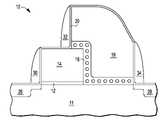
- FIG. 1illustrates, in cross-section, a semiconductor device 10 that is a partially completed NVM device.
- Semiconductor device 10 as shown In FIG. 1comprises a substrate 11 , gate dielectric 12 on substrate 11 , and a select gate portion 14 on gate dielectric 12 .
- Gate dielectric 12may be grown oxide or a high k dielectric or some other material suitable for a gate dielectric.
- Gate dielectricmay be a conventional, thermally formed silicon dioxide or silicon oxynitride with a thickness of less than 10 nanometers.
- gate dielectric 12may comprise an alternative gate material such as a first or second transition metal oxide or rare earth oxide material.
- Such alternative gate dielectric materialsare suitable for their high dielectric constant (K), which enables the use of a thicker gate dielectric layer without adversely affecting the electrical and capacitive characteristics of the film.
- One preferred high K gate dielectricis hafnium oxide (HfO 2 ).
- suitable transition metal oxide compositesselected from oxides of zirconium, hafnium, aluminum, lanthanum, strontium, tantalum, titanium, silicon and the combinations thereof may be used.
- Transition metal silicates and aluminatesmay also be used for the gate dielectric, such as hafnium silicate (Hf x Si y O z ) hafnium aluminate (Hf x Al y O z ).
- a polysilicon layeris formed over gate dielectric 12 etched using conventional deposition and etch processes to form select gate portion 14 so select gate portion 14 may also be called polysilicon layer 14 in this example. This leaves a portion of substrate 11 exposed.
- Storage layer 16Shown in FIG. 2 is semiconductor device 10 after a storage layer 16 has been deposited over select gate portion 14 and over the exposed portion of substrate 11 .
- Storage layer 16 as shownis a layer of nanocrystals but another type of storage layer useful in storing charge may be used instead.
- Nanocrystalsare typically formed of silicon, but the discrete storage elements may also be formed of clusters of material consisting of, for example, of germanium, silicon carbide, any number of metals, or in any combination.
- the charge storage materialmay consist of nitride, although any number of dielectrics containing traps may be used, such as aluminum oxide, zirconium oxide, hafnium oxide, tantalum oxide, lanthanum oxide, hafnium silicate, or hafnium aluminate.
- storage layer 16may be formed from a different material, such as for example, a floating gate formed from polysilicon.
- Amorphous silicon layer 18is preferably deposited by sputtering although it may be possible to deposit an effective amorphous silicon layer by a chemical vapor deposition (CVD) such as low-pressure or plasma enhanced CVD.
- CVDchemical vapor deposition
- Impuritiesmay be included in amorphous silicon layer 18 , such as nickel, gold, platinum, aluminum, copper, palladium, germanium, arsenic, and potentially other materials that combine with silicon to form a gate material that, when it converts from amorphous to polycrystalline, will be useful in generating a tensile stress on the charge storage layer.
- one or more of these impuritiesmay be included in a silicon target. Sputtering is particularly advantageous because of a relatively high density of deposited amorphous silicon which tends to expand when it is converted to polycrystalline form.
- FIG. 4Shown in FIG. 4 is semiconductor device 10 after etching amorphous silicon layer 18 and storage layer 16 from over polysilicon layer 14 .
- the etchis patterned so that a small portion of amorphous silicon layer 18 remains over polysilicon layer near a sidewall of polysilicon layer 14 where it is adjacent to a sidewall of amorphous silicon layer 18 .
- Charge storage layer 16is between polysilicon layer 14 and amorphous silicon layer 18 where they are adjacent.
- select gate portion 14 of FIGS. 1-4Shown in FIG. 5 is semiconductor device 10 after etching polysilicon layer 14 and amorphous layer 18 to leave select gate portion 14 of FIGS. 1-4 as a select gate.
- select gate portion 14has had a portion removed on the side away from amorphous silicon layer 18 .
- amorphous layerhas had a portion removed on the side away from select gate portion 14 . This results in exposing portions of substrate 11 on each side of the remaining portions of polysilicon layer 14 and amorphous silicon layer 18 .
- semiconductor device 10after forming an oxide liner 20 over semiconductor device 10 including the exposed portions of substrate 11 and exposed portions of polysilicon layer 14 and amorphous silicon layer 18 .
- the exposed portions of substrate 11are where source/drains are to be formed.
- semiconductor device 10after forming a stressor layer 22 over liner 20 and thus also over semiconductor device 10 including polysilicon layer 14 , amorphous silicon layer, and the substrate where source/drains are to be formed.
- Oxide liner 20needs to be deposited at a sufficiently low temperature to avoid prematurely converting amorphous silicon layer 18 to polysilicon.
- oxide linermay be deposited by a temperature known as low temperature oxide (LTO).
- Stressor layer 22should also be deposited at a sufficiently low temperature to avoid prematurely converting amorphous silicon layer 18 to polysilicon.
- Stressor layer 22may be nitride deposited by plasma-enhanced chemical vapor deposition (PECVD).
- PECVDplasma-enhanced chemical vapor
- FIG. 7Shown in FIG. 7 is semiconductor device 10 after performing an anneal 24 which is at a sufficiently high temperature to convert amorphous silicon layer 18 to a polysilicon control gate 19 .
- the conversion of amorphous to polysilicon, if unconstrained,will result in an increase in volume.
- the annealhas the effect of causing an outward pressure being applied to stressor layer 22 .
- the resultis a compressive stress in polysilicon control gate 19 , a tensile stress in the plane of charge storage layer 16 in the area under polysilicon control gate 19 , and a tensile stress in substrate 11 in the area under polysilicon layer 14 and polysilicon control gate 19 , which is where the channel of the completed NVM cell will be.
- Adding impurities to amorphous silicon layer 18can be useful increasing the added stress.
- the annealis preferably a rapid thermal anneal (RTA) and may be at a temperature in a range of from 500 to 1100 degrees Celsius.
- Shown in FIG. 8is semiconductor device 10 after removing stressor 22 .
- Stressor 22may be nitride which makes it relatively easy to remove selective to oxide layer 20 .
- Stressor 22preferably applies a tensile stress as deposited, but there may be situations in which there are reasons to apply a stressor with minimal or no stress but yet still achieve some benefit because of the amorphous to polysilicon conversion.
- the presence of stressor 22helps the transfer of stress to the substrate by constraining the expansion of amorphous layer 18 to polysilicon control gate 19 , but some beneficial stress may be transferred in the amorphous to polysilicon transfer even in the absence of a stressor layer.
- semiconductor device 10Shown in FIG. 9 is semiconductor device 10 with source/drain regions 26 and 28 on opposing sides of the channel region in substrate 11 under the select gate, which is polysilicon layer 14 of FIG. 9 , and polysilicon control gate 19 . Sidewall spacers 30 , 32 and 34 are also shown. Sidewall spacers 30 and 34 are useful in forming the heavily doped portions of source/drain regions 26 and 28 .
- Semiconductor device 10 of FIG. 9is a split gate NVM memory cell. Thus it is seen that an NVM cell, having a split gate, is able to achieve increased tensile stress and thus improve performance using the method described above.
- the methodincludes forming a gate dielectric over the semiconductor layer.
- the methodfurther includes forming a layer of gate material over the gate dielectric.
- the methodfurther includes etching the layer of gate material to form a select gate.
- the methodfurther includes forming a storage layer that extends over the select gate and over a portion of the semiconductor layer.
- the methodfurther includes depositing an amorphous silicon layer over the storage layer.
- the methodfurther includes etching the amorphous silicon layer to form a control gate.
- the methodfurther includes annealing the semiconductor device to crystallize the amorphous silicon layer.
- the methodmay further comprise forming a capping layer over the semiconductor device, the capping layer formed prior to the step of annealing the semiconductor device.
- the methodmay further comprise removing the capping layer from over the semiconductor device after the step of annealing the semiconductor device.
- the methodmay further be characterized by forming the capping layer further comprising forming a capping layer that causes a channel region in the semiconductor layer to be laterally tensile stressed.
- the methodmay further be characterized by forming the capping layer further comprising forming the capping layer from tensile stressed silicon nitride.
- the methodmay further be characterized by the step of depositing a silicon layer comprising sputtering silicon and an impurity, wherein the impurity comprises one of group consisting of nickel, gold, aluminum, silver, and palladium.
- the methodmay further be characterized by annealing the semiconductor device to crystallize the amorphous silicon layer further comprising annealing the semiconductor device at a temperature in a range of 500 to 1100 degrees Celsius.
- the methodmay further be characterized by depositing the amorphous silicon layer over the storage layer further comprising depositing the amorphous silicon layer to have a thickness in a range of 50 to 250 nanometers.
- the methodmay further be characterized by etching the amorphous silicon layer to form the control gate further comprising etching the amorphous silicon layer to form the control gate having a portion formed over a portion of the select gate.
- the methodmay further be characterized by forming the storage layer being further characterized by the storage layer comprising nanocrystals.
- the methodmay further be characterized by the step of depositing the amorphous silicon layer being performed by sputtering.
- the methodincludes forming a gate dielectric over the semiconductor layer.
- the methodfurther includes forming a layer of gate material over the gate dielectric.
- the methodfurther includes etching the layer of gate material to form a select gate.
- the methodfurther includes forming a charge storage layer that extends over the select gate and over a portion of the semiconductor layer.
- the methodfurther includes depositing an amorphous silicon layer over the charge storage layer.
- the methodfurther includes etching the amorphous silicon layer to form a control gate.
- the methodfurther includes forming a liner on the semiconductor device.
- the methodfurther includes forming a capping layer over the liner.
- the methodfurther includes annealing the semiconductor device to crystallize the amorphous silicon layer.
- the methodmay further comprise removing the capping layer from over the semiconductor device after the step of annealing the semiconductor device.
- the methodmay be further characterized by forming the capping layer further comprising forming the capping layer from tensile stressed silicon nitride.
- the methodmay be further characterized by forming the capping layer further comprising depositing a silicon nitride layer having a thickness in a range of 20 to 200 nanometers.
- the methodmay be further characterized by annealing the semiconductor device to crystallize the amorphous silicon layer further comprising annealing the semiconductor device at a temperature in a range of 500 to 1100 degrees Celsius.
- the methodmay be further characterized by depositing the amorphous silicon layer over the storage layer being further characterized by sputtering silicon and an impurity.
- the methodmay be further characterized by forming the charge storage layer being further characterized by the charge storage layer comprising nanocrystals.
- the methodincludes forming a gate dielectric over the semiconductor layer.
- the methodfurther includes forming a polysilicon layer over the gate dielectric.
- the methodfurther includes etching the polysilicon layer to form a select gate.
- the methodfurther includes forming a charge storage layer that extends over the select gate and over a portion of the semiconductor layer, wherein the charge storage layer comprises nanocrystals.
- the methodfurther includes depositing an amorphous silicon layer over the charge storage layer.
- the methodfurther includes etching the amorphous silicon layer to form a control gate, the control gate having a portion formed over a portion of the select gate.
- the methodfurther includes forming an insulating liner on the semiconductor device.
- the methodfurther includes forming a tensile stressed silicon nitride layer over the insulating liner.
- the methodfurther includes annealing the semiconductor device to crystallize the amorphous silicon layer.
- the methodfurther includes removing the tensile stressed silicon nitride layer.
- the methodmay be further characterized by forming the silicon nitride layer further comprising depositing a silicon nitride layer having a thickness in a range of 20 to 200 nanometers, annealing the semiconductor device to crystallize the amorphous silicon layer further comprising annealing the semiconductor device at a temperature in a range of 500 to 1100 degrees Celsius, and depositing the amorphous silicon layer over the charge storage layer being by sputtering
Landscapes
- Engineering & Computer Science (AREA)
- Chemical & Material Sciences (AREA)
- Nanotechnology (AREA)
- Physics & Mathematics (AREA)
- Mathematical Physics (AREA)
- Theoretical Computer Science (AREA)
- Crystallography & Structural Chemistry (AREA)
- Non-Volatile Memory (AREA)
- Semiconductor Memories (AREA)
Abstract
Description
- This invention is related to application serial number (docket number MT11251TP); titled “Stressed Semiconductor Device and Method for Making” by Konstantin Loiko, Cheong Min Hong, Sung-Taeg Kang, Taras Kirichenko, and Brian Winstead; assigned to the assignee hereof; and filed on even date herewith.
- 1. Field
- This disclosure relates generally to memories, and more specifically, to a method for making a stressed non-volatile memory device.
- 2. Related Art
- Semiconductor non-volatile memories (NVMs), and particularly flash electrically erasable, programmable read-only memories (EEPROMs), are widely used in a range of electronic equipment from computers, to telecommunications hardware, to consumer appliances. The flash EEPROM is encountered in numerous configurations. In particular, a floating-gate NVM cell is characterized by a stacked gate construction in which a floating gate, typically formed from polysilicon, is separated from the substrate by a first (lower) oxide layer and is separated from a polysilicon control gate by a second (upper) oxide layer. No direct electrical connection is made to the floating gate (hence, “floating”).
- In another configuration, a charge storage layer comprising nanocrystals as the charge storage mechanism is used in place of the floating gate. The nanocrystals function as isolated charge storage elements.
- As devices continue to become smaller with advances in semiconductor device technology, the performance of the individual memory cells has become more important. The read function in particular suffers with reduced device performance.
- In many prior art non-volatile memory (NVM) devices, the charge storage layer is separated from the channel region by a relatively thin tunnel dielectric layer. There can be a problem of charge leakage from the charge storage layer to the underlying channel. Such charge leakage can lead to degradation of the memory state stored within the device and is therefore undesirable. In order to avoid such charge leakage, the thickness of the tunnel dielectric is often increased. However, a thicker tunnel dielectric requires higher programming and erasing voltages for storing and removing charge from the charge storage layer as the charge carriers must pass through the thicker tunnel dielectric. In many cases, higher programming voltages increase power consumption and may require the implementation of charge pumps in order to increase the supply voltage to meet programming voltage requirements. Such charge pumps consume a significant amount of die area for the integrated circuit and therefore reduce the memory array area efficiency and increase overall costs.
- Therefore, what is needed is a NVM cell with improved performance.
- The present invention is illustrated by way of example and is not limited by the accompanying figures, in which like references indicate similar elements. Elements in the figures are illustrated for simplicity and clarity and have not necessarily been drawn to scale.
FIG. 1 is a cross section of a semiconductor device at a stage in processing according to an embodiment;FIG. 2 is a cross section of the semiconductor device ofFIG. 1 at a subsequent stage in processing;FIG. 3 is a cross section of the semiconductor device ofFIG. 2 at a subsequent stage in processing;FIG. 4 is a cross section of the semiconductor device ofFIG. 3 at a subsequent stage in processing;FIG. 5 is a cross section of the semiconductor device ofFIG. 4 at a subsequent stage in processing;FIG. 6 is a cross section of the semiconductor device ofFIG. 5 at a subsequent stage in processing;FIG. 7 is a cross section of the semiconductor device ofFIG. 6 at a subsequent stage in processing;FIG. 8 is a cross section of the semiconductor device ofFIG. 7 at a subsequent stage in processing; andFIG. 9 is a cross section of the semiconductor device ofFIG. 8 at a subsequent stage in processing as a non-volatile memory cell;- In one aspect, a split-gate NVM cell has enhanced performance by having a stressed charge storage layer as a result of a change of the control gate changing from amorphous silicon to polysilicon while a stressor layer is over both the control gate and the select gate before source/drain formation. The stress changes the energy barrier height between the bottom insulator and the nanocrystals of the charge storage layer gate. The stress may also increase the effective mass in the nanocrystals of the charge storage layer. The higher energy barrier and increased effective mass improve data retention of the nanocrystals by reducing a leakage current from the charge storage layer to the channel region. The conversion from amorphous to polysilicon is achieved with an anneal that has the effect of applying tensile stress in the plane of the charge storage layer. This is better understood by reference to the drawings and the following description.
- The semiconductor substrate described herein can be any semiconductor material or combinations of materials, such as gallium arsenide, silicon germanium, silicon-on-insulator (SOI), silicon, monocrystalline silicon, the like, and combinations of the above.
- Shown in
FIG. 1 illustrates, in cross-section, asemiconductor device 10 that is a partially completed NVM device.Semiconductor device 10 as shown InFIG. 1 comprises asubstrate 11, gate dielectric12 onsubstrate 11, and aselect gate portion 14 on gate dielectric12. Gate dielectric12 may be grown oxide or a high k dielectric or some other material suitable for a gate dielectric. Gate dielectric may be a conventional, thermally formed silicon dioxide or silicon oxynitride with a thickness of less than 10 nanometers. In another embodiment, gate dielectric12 may comprise an alternative gate material such as a first or second transition metal oxide or rare earth oxide material. Such alternative gate dielectric materials are suitable for their high dielectric constant (K), which enables the use of a thicker gate dielectric layer without adversely affecting the electrical and capacitive characteristics of the film. One preferred high K gate dielectric is hafnium oxide (HfO2). For these alternative gate dielectrics, suitable transition metal oxide composites selected from oxides of zirconium, hafnium, aluminum, lanthanum, strontium, tantalum, titanium, silicon and the combinations thereof may be used. Transition metal silicates and aluminates may also be used for the gate dielectric, such as hafnium silicate (HfxSiyOz) hafnium aluminate (HfxAlyOz). A polysilicon layer is formed over gate dielectric12 etched using conventional deposition and etch processes to formselect gate portion 14 soselect gate portion 14 may also be calledpolysilicon layer 14 in this example. This leaves a portion ofsubstrate 11 exposed. - Shown in
FIG. 2 issemiconductor device 10 after astorage layer 16 has been deposited overselect gate portion 14 and over the exposed portion ofsubstrate 11.Storage layer 16 as shown is a layer of nanocrystals but another type of storage layer useful in storing charge may be used instead. Nanocrystals are typically formed of silicon, but the discrete storage elements may also be formed of clusters of material consisting of, for example, of germanium, silicon carbide, any number of metals, or in any combination. Alternately, the charge storage material may consist of nitride, although any number of dielectrics containing traps may be used, such as aluminum oxide, zirconium oxide, hafnium oxide, tantalum oxide, lanthanum oxide, hafnium silicate, or hafnium aluminate. In another embodiment,storage layer 16 may be formed from a different material, such as for example, a floating gate formed from polysilicon. - Shown in
FIG. 3 issemiconductor device 10 after depositing anamorphous silicon layer 18, which may be doped or undoped, overstorage layer 16.Amorphous silicon layer 18 is preferably deposited by sputtering although it may be possible to deposit an effective amorphous silicon layer by a chemical vapor deposition (CVD) such as low-pressure or plasma enhanced CVD. Impurities may be included inamorphous silicon layer 18, such as nickel, gold, platinum, aluminum, copper, palladium, germanium, arsenic, and potentially other materials that combine with silicon to form a gate material that, when it converts from amorphous to polycrystalline, will be useful in generating a tensile stress on the charge storage layer. In the case of sputtering, one or more of these impurities may be included in a silicon target. Sputtering is particularly advantageous because of a relatively high density of deposited amorphous silicon which tends to expand when it is converted to polycrystalline form. - Shown in
FIG. 4 issemiconductor device 10 after etchingamorphous silicon layer 18 andstorage layer 16 from overpolysilicon layer 14. The etch is patterned so that a small portion ofamorphous silicon layer 18 remains over polysilicon layer near a sidewall ofpolysilicon layer 14 where it is adjacent to a sidewall ofamorphous silicon layer 18.Charge storage layer 16 is betweenpolysilicon layer 14 andamorphous silicon layer 18 where they are adjacent. - Shown in
FIG. 5 issemiconductor device 10 after etchingpolysilicon layer 14 andamorphous layer 18 to leaveselect gate portion 14 ofFIGS. 1-4 as a select gate. As shown inFIG. 5 , selectgate portion 14 has had a portion removed on the side away fromamorphous silicon layer 18. Similarly, amorphous layer has had a portion removed on the side away fromselect gate portion 14. This results in exposing portions ofsubstrate 11 on each side of the remaining portions ofpolysilicon layer 14 andamorphous silicon layer 18. - Shown in
FIG. 6 issemiconductor device 10 after forming anoxide liner 20 oversemiconductor device 10 including the exposed portions ofsubstrate 11 and exposed portions ofpolysilicon layer 14 andamorphous silicon layer 18. The exposed portions ofsubstrate 11 are where source/drains are to be formed. Also shown issemiconductor device 10 after forming astressor layer 22 overliner 20 and thus also oversemiconductor device 10 includingpolysilicon layer 14, amorphous silicon layer, and the substrate where source/drains are to be formed.Oxide liner 20 needs to be deposited at a sufficiently low temperature to avoid prematurely convertingamorphous silicon layer 18 to polysilicon. For example, oxide liner may be deposited by a temperature known as low temperature oxide (LTO).Stressor layer 22 should also be deposited at a sufficiently low temperature to avoid prematurely convertingamorphous silicon layer 18 to polysilicon.Stressor layer 22 may be nitride deposited by plasma-enhanced chemical vapor deposition (PECVD). - Shown in
FIG. 7 issemiconductor device 10 after performing ananneal 24 which is at a sufficiently high temperature to convertamorphous silicon layer 18 to apolysilicon control gate 19. The conversion of amorphous to polysilicon, if unconstrained, will result in an increase in volume. Thus the anneal has the effect of causing an outward pressure being applied tostressor layer 22. Although the mechanism is not certain, the result is a compressive stress inpolysilicon control gate 19, a tensile stress in the plane ofcharge storage layer 16 in the area underpolysilicon control gate 19, and a tensile stress insubstrate 11 in the area underpolysilicon layer 14 andpolysilicon control gate 19, which is where the channel of the completed NVM cell will be. Adding impurities toamorphous silicon layer 18 can be useful increasing the added stress. The anneal is preferably a rapid thermal anneal (RTA) and may be at a temperature in a range of from 500 to 1100 degrees Celsius. - Shown in
FIG. 8 issemiconductor device 10 after removingstressor 22. Although the mechanism is not well understood, the stress generated by this process is effective and retained even afterstressor layer 22 is removed.Stressor 22 may be nitride which makes it relatively easy to remove selective tooxide layer 20.Stressor 22 preferably applies a tensile stress as deposited, but there may be situations in which there are reasons to apply a stressor with minimal or no stress but yet still achieve some benefit because of the amorphous to polysilicon conversion. The presence ofstressor 22 helps the transfer of stress to the substrate by constraining the expansion ofamorphous layer 18 topolysilicon control gate 19, but some beneficial stress may be transferred in the amorphous to polysilicon transfer even in the absence of a stressor layer. - Shown in
FIG. 9 issemiconductor device 10 with source/drain regions substrate 11 under the select gate, which ispolysilicon layer 14 ofFIG. 9 , andpolysilicon control gate 19.Sidewall spacers Sidewall spacers drain regions Semiconductor device 10 ofFIG. 9 is a split gate NVM memory cell. Thus it is seen that an NVM cell, having a split gate, is able to achieve increased tensile stress and thus improve performance using the method described above. - By now it should be apparent that a method of making a semiconductor device on a semiconductor layer has been described. The method includes forming a gate dielectric over the semiconductor layer. The method further includes forming a layer of gate material over the gate dielectric. The method further includes etching the layer of gate material to form a select gate. The method further includes forming a storage layer that extends over the select gate and over a portion of the semiconductor layer. The method further includes depositing an amorphous silicon layer over the storage layer. The method further includes etching the amorphous silicon layer to form a control gate. The method further includes annealing the semiconductor device to crystallize the amorphous silicon layer. The method may further comprise forming a capping layer over the semiconductor device, the capping layer formed prior to the step of annealing the semiconductor device. The method may further comprise removing the capping layer from over the semiconductor device after the step of annealing the semiconductor device. The method may further be characterized by forming the capping layer further comprising forming a capping layer that causes a channel region in the semiconductor layer to be laterally tensile stressed. The method may further be characterized by forming the capping layer further comprising forming the capping layer from tensile stressed silicon nitride. The method may further be characterized by the step of depositing a silicon layer comprising sputtering silicon and an impurity, wherein the impurity comprises one of group consisting of nickel, gold, aluminum, silver, and palladium. The method may further be characterized by annealing the semiconductor device to crystallize the amorphous silicon layer further comprising annealing the semiconductor device at a temperature in a range of 500 to 1100 degrees Celsius. The method may further be characterized by depositing the amorphous silicon layer over the storage layer further comprising depositing the amorphous silicon layer to have a thickness in a range of 50 to 250 nanometers. The method may further be characterized by etching the amorphous silicon layer to form the control gate further comprising etching the amorphous silicon layer to form the control gate having a portion formed over a portion of the select gate. The method may further be characterized by forming the storage layer being further characterized by the storage layer comprising nanocrystals. The method may further be characterized by the step of depositing the amorphous silicon layer being performed by sputtering.
- Also described is a method of making a semiconductor device on a semiconductor layer. The method includes forming a gate dielectric over the semiconductor layer. The method further includes forming a layer of gate material over the gate dielectric. The method further includes etching the layer of gate material to form a select gate. The method further includes forming a charge storage layer that extends over the select gate and over a portion of the semiconductor layer. The method further includes depositing an amorphous silicon layer over the charge storage layer. The method further includes etching the amorphous silicon layer to form a control gate. The method further includes forming a liner on the semiconductor device. The method further includes forming a capping layer over the liner. The method further includes annealing the semiconductor device to crystallize the amorphous silicon layer. The method may further comprise removing the capping layer from over the semiconductor device after the step of annealing the semiconductor device. The method may be further characterized by forming the capping layer further comprising forming the capping layer from tensile stressed silicon nitride. The method may be further characterized by forming the capping layer further comprising depositing a silicon nitride layer having a thickness in a range of 20 to 200 nanometers. The method may be further characterized by annealing the semiconductor device to crystallize the amorphous silicon layer further comprising annealing the semiconductor device at a temperature in a range of 500 to 1100 degrees Celsius. The method may be further characterized by depositing the amorphous silicon layer over the storage layer being further characterized by sputtering silicon and an impurity. The method may be further characterized by forming the charge storage layer being further characterized by the charge storage layer comprising nanocrystals.
- Described also is a method of making a semiconductor device on a semiconductor layer. The method includes forming a gate dielectric over the semiconductor layer. The method further includes forming a polysilicon layer over the gate dielectric. The method further includes etching the polysilicon layer to form a select gate. The method further includes forming a charge storage layer that extends over the select gate and over a portion of the semiconductor layer, wherein the charge storage layer comprises nanocrystals. The method further includes depositing an amorphous silicon layer over the charge storage layer. The method further includes etching the amorphous silicon layer to form a control gate, the control gate having a portion formed over a portion of the select gate. The method further includes forming an insulating liner on the semiconductor device. The method further includes forming a tensile stressed silicon nitride layer over the insulating liner. The method further includes annealing the semiconductor device to crystallize the amorphous silicon layer. The method further includes removing the tensile stressed silicon nitride layer. The method may be further characterized by forming the silicon nitride layer further comprising depositing a silicon nitride layer having a thickness in a range of 20 to 200 nanometers, annealing the semiconductor device to crystallize the amorphous silicon layer further comprising annealing the semiconductor device at a temperature in a range of 500 to 1100 degrees Celsius, and depositing the amorphous silicon layer over the charge storage layer being by sputtering
- Although the invention is described herein with reference to specific embodiments, various modifications and changes can be made without departing from the scope of the present invention as set forth in the claims below. For example, different processes may be used for obtaining some of the temporary structures obtained in order to make effective use of the conversion from amorphous silicon to polysilicon. Accordingly, the specification and figures are to be regarded in an illustrative rather than a restrictive sense, and all such modifications are intended to be included within the scope of the present invention. Any benefits, advantages, or solutions to problems that are described herein with regard to specific embodiments are not intended to be construed as a critical, required, or essential feature or element of any or all the claims.
- Furthermore, the terms “a” or “an,” as used herein, are defined as one or more than one. Also, the use of introductory phrases such as “at least one” and “one or more” in the claims should not be construed to imply that the introduction of another claim element by the indefinite articles “a” or “an” limits any particular claim containing such introduced claim element to inventions containing only one such element, even when the same claim includes the introductory phrases “one or more” or “at least one” and indefinite articles such as “a” or “an.” The same holds true for the use of definite articles.
- Unless stated otherwise, terms such as “first” and “second” are used to arbitrarily distinguish between the elements such terms describe. Thus, these terms are not necessarily intended to indicate temporal or other prioritization of such elements.
Claims (20)
Priority Applications (1)
| Application Number | Priority Date | Filing Date | Title |
|---|---|---|---|
| US12/414,778US7960267B2 (en) | 2009-03-31 | 2009-03-31 | Method for making a stressed non-volatile memory device |
Applications Claiming Priority (1)
| Application Number | Priority Date | Filing Date | Title |
|---|---|---|---|
| US12/414,778US7960267B2 (en) | 2009-03-31 | 2009-03-31 | Method for making a stressed non-volatile memory device |
Publications (2)
| Publication Number | Publication Date |
|---|---|
| US20100248466A1true US20100248466A1 (en) | 2010-09-30 |
| US7960267B2 US7960267B2 (en) | 2011-06-14 |
Family
ID=42784797
Family Applications (1)
| Application Number | Title | Priority Date | Filing Date |
|---|---|---|---|
| US12/414,778Expired - Fee RelatedUS7960267B2 (en) | 2009-03-31 | 2009-03-31 | Method for making a stressed non-volatile memory device |
Country Status (1)
| Country | Link |
|---|---|
| US (1) | US7960267B2 (en) |
Cited By (6)
| Publication number | Priority date | Publication date | Assignee | Title |
|---|---|---|---|---|
| US20120052670A1 (en)* | 2010-08-31 | 2012-03-01 | Shroff Mehul D | Patterning a gate stack of a non-volatile memory (nvm) with simultaneous etch in non-nvm area |
| US8557650B2 (en) | 2010-08-31 | 2013-10-15 | Freescale Semiconductor, Inc. | Patterning a gate stack of a non-volatile memory (NVM) using a dummy gate stack |
| US9257445B2 (en)* | 2014-05-30 | 2016-02-09 | Freescale Semiconductor, Inc. | Method of making a split gate non-volatile memory (NVM) cell and a logic transistor |
| US20180337123A1 (en)* | 2016-01-13 | 2018-11-22 | Taiwan Semiconductor Manufacturing Company, Ltd. | Capacitor Embedded with Nanocrystals |
| US20190181149A1 (en)* | 2017-03-13 | 2019-06-13 | Taiwan Semiconductor Manufacturing Co., Ltd. | Method of manufacturing semiconductor device having multi-height structure |
| US20200027996A1 (en)* | 2018-07-17 | 2020-01-23 | Renesas Electronics Corporation | Semiconductor device and a method of manufacturing the same |
Families Citing this family (2)
| Publication number | Priority date | Publication date | Assignee | Title |
|---|---|---|---|---|
| US20140209995A1 (en)* | 2013-01-29 | 2014-07-31 | Cheong Min Hong | Non-Volatile Memory Cells Having Carbon Impurities and Related Manufacturing Methods |
| US20140357072A1 (en)* | 2013-05-31 | 2014-12-04 | Jinmiao J. Shen | Methods and structures for split gate memory |
Citations (16)
| Publication number | Priority date | Publication date | Assignee | Title |
|---|---|---|---|---|
| US5408115A (en)* | 1994-04-04 | 1995-04-18 | Motorola Inc. | Self-aligned, split-gate EEPROM device |
| US20030034517A1 (en)* | 2000-10-06 | 2003-02-20 | Bin-Shing Chen | Structure of split-gate eeprom memory cell |
| US6875660B2 (en)* | 2003-02-26 | 2005-04-05 | Powerchip Semiconductor Corp. | Method of manufacturing high coupling ratio flash memory having sidewall spacer floating gate electrode |
| US20050104115A1 (en)* | 2002-04-01 | 2005-05-19 | Sohrab Kianian | Self aligned method of forming a semiconductor memory array of floating gate memory cells with buried bit-line and raised source line, and a memory array made thereby |
| US20070132054A1 (en)* | 2005-12-13 | 2007-06-14 | Applied Materials | Memory cell having stressed layers |
| US7235441B2 (en)* | 2003-10-20 | 2007-06-26 | Renesas Technology Corp. | Nonvolatile semiconductor memory device with tapered sidewall gate and method of manufacturing the same |
| US20080042183A1 (en)* | 2006-08-16 | 2008-02-21 | Nima Mokhlesi | Nonvolatile Memories with Shaped Floating Gates |
| US20080142871A1 (en)* | 2003-10-23 | 2008-06-19 | Fujitsu Limited | Semiconductor device and method for manufacturing semiconductor device |
| US20080188052A1 (en)* | 2007-02-06 | 2008-08-07 | Winstead Brian A | Split-gate thin film storage NVM cell with reduced load-up/trap-up effects |
| US7436019B2 (en)* | 2004-03-12 | 2008-10-14 | Sandisk Corporation | Non-volatile memory cells shaped to increase coupling to word lines |
| US20080261385A1 (en)* | 2007-04-20 | 2008-10-23 | Dharmesh Jawarani | Method for selective removal of a layer |
| US7446370B2 (en)* | 2006-04-20 | 2008-11-04 | Powerchip Semiconductor Corp. | Non-volatile memory |
| US7494860B2 (en)* | 2006-08-16 | 2009-02-24 | Sandisk Corporation | Methods of forming nonvolatile memories with L-shaped floating gates |
| US20090072294A1 (en)* | 2006-10-16 | 2009-03-19 | Samsung Electronics Co., Ltd. | Method of manufacturing a non-volatile memory device |
| US7557402B2 (en)* | 2004-06-17 | 2009-07-07 | Taiwan Semiconductor Manufacturing Company, Ltd. | High write and erase efficiency embedded flash cell |
| US7700439B2 (en)* | 2006-03-15 | 2010-04-20 | Freescale Semiconductor, Inc. | Silicided nonvolatile memory and method of making same |
- 2009
- 2009-03-31USUS12/414,778patent/US7960267B2/ennot_activeExpired - Fee Related
Patent Citations (16)
| Publication number | Priority date | Publication date | Assignee | Title |
|---|---|---|---|---|
| US5408115A (en)* | 1994-04-04 | 1995-04-18 | Motorola Inc. | Self-aligned, split-gate EEPROM device |
| US20030034517A1 (en)* | 2000-10-06 | 2003-02-20 | Bin-Shing Chen | Structure of split-gate eeprom memory cell |
| US20050104115A1 (en)* | 2002-04-01 | 2005-05-19 | Sohrab Kianian | Self aligned method of forming a semiconductor memory array of floating gate memory cells with buried bit-line and raised source line, and a memory array made thereby |
| US6875660B2 (en)* | 2003-02-26 | 2005-04-05 | Powerchip Semiconductor Corp. | Method of manufacturing high coupling ratio flash memory having sidewall spacer floating gate electrode |
| US7235441B2 (en)* | 2003-10-20 | 2007-06-26 | Renesas Technology Corp. | Nonvolatile semiconductor memory device with tapered sidewall gate and method of manufacturing the same |
| US20080142871A1 (en)* | 2003-10-23 | 2008-06-19 | Fujitsu Limited | Semiconductor device and method for manufacturing semiconductor device |
| US7436019B2 (en)* | 2004-03-12 | 2008-10-14 | Sandisk Corporation | Non-volatile memory cells shaped to increase coupling to word lines |
| US7557402B2 (en)* | 2004-06-17 | 2009-07-07 | Taiwan Semiconductor Manufacturing Company, Ltd. | High write and erase efficiency embedded flash cell |
| US20070132054A1 (en)* | 2005-12-13 | 2007-06-14 | Applied Materials | Memory cell having stressed layers |
| US7700439B2 (en)* | 2006-03-15 | 2010-04-20 | Freescale Semiconductor, Inc. | Silicided nonvolatile memory and method of making same |
| US7446370B2 (en)* | 2006-04-20 | 2008-11-04 | Powerchip Semiconductor Corp. | Non-volatile memory |
| US7494860B2 (en)* | 2006-08-16 | 2009-02-24 | Sandisk Corporation | Methods of forming nonvolatile memories with L-shaped floating gates |
| US20080042183A1 (en)* | 2006-08-16 | 2008-02-21 | Nima Mokhlesi | Nonvolatile Memories with Shaped Floating Gates |
| US20090072294A1 (en)* | 2006-10-16 | 2009-03-19 | Samsung Electronics Co., Ltd. | Method of manufacturing a non-volatile memory device |
| US20080188052A1 (en)* | 2007-02-06 | 2008-08-07 | Winstead Brian A | Split-gate thin film storage NVM cell with reduced load-up/trap-up effects |
| US20080261385A1 (en)* | 2007-04-20 | 2008-10-23 | Dharmesh Jawarani | Method for selective removal of a layer |
Cited By (10)
| Publication number | Priority date | Publication date | Assignee | Title |
|---|---|---|---|---|
| US20120052670A1 (en)* | 2010-08-31 | 2012-03-01 | Shroff Mehul D | Patterning a gate stack of a non-volatile memory (nvm) with simultaneous etch in non-nvm area |
| US8202778B2 (en)* | 2010-08-31 | 2012-06-19 | Freescale Semiconductor, Inc. | Patterning a gate stack of a non-volatile memory (NVM) with simultaneous etch in non-NVM area |
| US8557650B2 (en) | 2010-08-31 | 2013-10-15 | Freescale Semiconductor, Inc. | Patterning a gate stack of a non-volatile memory (NVM) using a dummy gate stack |
| US9257445B2 (en)* | 2014-05-30 | 2016-02-09 | Freescale Semiconductor, Inc. | Method of making a split gate non-volatile memory (NVM) cell and a logic transistor |
| US20180337123A1 (en)* | 2016-01-13 | 2018-11-22 | Taiwan Semiconductor Manufacturing Company, Ltd. | Capacitor Embedded with Nanocrystals |
| US10930583B2 (en)* | 2016-01-13 | 2021-02-23 | Taiwan Semiconductor Manufacturing Company, Ltd. | Capacitor embedded with nanocrystals |
| US20190181149A1 (en)* | 2017-03-13 | 2019-06-13 | Taiwan Semiconductor Manufacturing Co., Ltd. | Method of manufacturing semiconductor device having multi-height structure |
| US10672777B2 (en)* | 2017-03-13 | 2020-06-02 | Taiwan Semiconductor Manufacturing Co., Ltd. | Method of manufacturing semiconductor device having multi-height structure |
| US20200027996A1 (en)* | 2018-07-17 | 2020-01-23 | Renesas Electronics Corporation | Semiconductor device and a method of manufacturing the same |
| US11094833B2 (en)* | 2018-07-17 | 2021-08-17 | Renesas Electronics Corporation | Semiconductor device including memory using hafnium and a method of manufacturing the same |
Also Published As
| Publication number | Publication date |
|---|---|
| US7960267B2 (en) | 2011-06-14 |
Similar Documents
| Publication | Publication Date | Title |
|---|---|---|
| US7960267B2 (en) | Method for making a stressed non-volatile memory device | |
| US10541252B2 (en) | Memory arrays, and methods of forming memory arrays | |
| US7821055B2 (en) | Stressed semiconductor device and method for making | |
| US8687426B2 (en) | Multi-semiconductor material vertical memory strings, strings of memory cells having individually biasable channel regions, memory arrays incorporating such strings, and methods of accesssing and forming the same | |
| US7138681B2 (en) | High density stepped, non-planar nitride read only memory | |
| US7550341B2 (en) | High density stepped, non-planar flash memory | |
| US11482534B2 (en) | Integrated structures and methods of forming vertically-stacked memory cells | |
| US8263463B2 (en) | Nonvolatile split gate memory cell having oxide growth | |
| US20090134450A1 (en) | Tunneling insulating layer, flash memory device including the same, memory card and system including the flash memory device, and methods of manufacturing the same | |
| US7388251B2 (en) | Non-planar flash memory array with shielded floating gates on silicon mesas | |
| CN102282651A (en) | Memory transistor with a non-planar floating gate and manufacturing method thereof | |
| WO2010066126A1 (en) | Method for manufacturing split gate type flash memory | |
| US11133422B2 (en) | Method for manufacturing a semiconductor device | |
| CN103180952B (en) | Getters in memory charge storage structures | |
| CN100444402C (en) | Semiconductor device with a plurality of semiconductor chips | |
| US7645663B2 (en) | Method of producing non volatile memory device | |
| KR100905276B1 (en) | Flash memory device including multylayer tunnel insulator and method of fabricating the same | |
| EP4576977A1 (en) | Memory cell for a 3d nand flash memory | |
| KR100831976B1 (en) | Nonvolatile Memory Device and Manufacturing Method Thereof | |
| US20130102143A1 (en) | Method of making a non-volatile memory cell having a floating gate | |
| US20160190349A1 (en) | e-Flash Si Dot Nitrogen Passivation for Trap Reduction | |
| US20150129951A1 (en) | Method of forming semiconductor structure of control gate, and semiconductor device | |
| KR20090000315A (en) | Semiconductor memory device and manufacturing method thereof |
Legal Events
| Date | Code | Title | Description |
|---|---|---|---|
| AS | Assignment | Owner name:FREESCALE SEMICONDUCTOR, INC., TEXAS Free format text:ASSIGNMENT OF ASSIGNORS INTEREST;ASSIGNORS:LOIKO, KONSTANTIN V.;WINSTEAD, BRIAN A.;KIRICHENKO, TARAS A.;REEL/FRAME:022475/0649 Effective date:20090325 | |
| AS | Assignment | Owner name:CITIBANK, N.A., NEW YORK Free format text:SECURITY AGREEMENT;ASSIGNOR:FREESCALE SEMICONDUCTOR, INC.;REEL/FRAME:022703/0405 Effective date:20090428 | |
| STCF | Information on status: patent grant | Free format text:PATENTED CASE | |
| AS | Assignment | Owner name:CITIBANK, N.A., AS NOTES COLLATERAL AGENT, NEW YORK Free format text:SECURITY AGREEMENT;ASSIGNOR:FREESCALE SEMICONDUCTOR, INC.;REEL/FRAME:030633/0424 Effective date:20130521 Owner name:CITIBANK, N.A., AS NOTES COLLATERAL AGENT, NEW YOR Free format text:SECURITY AGREEMENT;ASSIGNOR:FREESCALE SEMICONDUCTOR, INC.;REEL/FRAME:030633/0424 Effective date:20130521 | |
| AS | Assignment | Owner name:CITIBANK, N.A., AS NOTES COLLATERAL AGENT, NEW YORK Free format text:SECURITY AGREEMENT;ASSIGNOR:FREESCALE SEMICONDUCTOR, INC.;REEL/FRAME:031591/0266 Effective date:20131101 Owner name:CITIBANK, N.A., AS NOTES COLLATERAL AGENT, NEW YOR Free format text:SECURITY AGREEMENT;ASSIGNOR:FREESCALE SEMICONDUCTOR, INC.;REEL/FRAME:031591/0266 Effective date:20131101 | |
| FPAY | Fee payment | Year of fee payment:4 | |
| AS | Assignment | Owner name:FREESCALE SEMICONDUCTOR, INC., TEXAS Free format text:PATENT RELEASE;ASSIGNOR:CITIBANK, N.A., AS COLLATERAL AGENT;REEL/FRAME:037354/0793 Effective date:20151207 | |
| AS | Assignment | Owner name:MORGAN STANLEY SENIOR FUNDING, INC., MARYLAND Free format text:ASSIGNMENT AND ASSUMPTION OF SECURITY INTEREST IN PATENTS;ASSIGNOR:CITIBANK, N.A.;REEL/FRAME:037486/0517 Effective date:20151207 | |
| AS | Assignment | Owner name:MORGAN STANLEY SENIOR FUNDING, INC., MARYLAND Free format text:ASSIGNMENT AND ASSUMPTION OF SECURITY INTEREST IN PATENTS;ASSIGNOR:CITIBANK, N.A.;REEL/FRAME:037518/0292 Effective date:20151207 | |
| AS | Assignment | Owner name:MORGAN STANLEY SENIOR FUNDING, INC., MARYLAND Free format text:SUPPLEMENT TO THE SECURITY AGREEMENT;ASSIGNOR:FREESCALE SEMICONDUCTOR, INC.;REEL/FRAME:039138/0001 Effective date:20160525 | |
| AS | Assignment | Owner name:NXP, B.V., F/K/A FREESCALE SEMICONDUCTOR, INC., NETHERLANDS Free format text:RELEASE BY SECURED PARTY;ASSIGNOR:MORGAN STANLEY SENIOR FUNDING, INC.;REEL/FRAME:040925/0001 Effective date:20160912 Owner name:NXP, B.V., F/K/A FREESCALE SEMICONDUCTOR, INC., NE Free format text:RELEASE BY SECURED PARTY;ASSIGNOR:MORGAN STANLEY SENIOR FUNDING, INC.;REEL/FRAME:040925/0001 Effective date:20160912 | |
| AS | Assignment | Owner name:NXP B.V., NETHERLANDS Free format text:RELEASE BY SECURED PARTY;ASSIGNOR:MORGAN STANLEY SENIOR FUNDING, INC.;REEL/FRAME:040928/0001 Effective date:20160622 | |
| AS | Assignment | Owner name:NXP USA, INC., TEXAS Free format text:CHANGE OF NAME;ASSIGNOR:FREESCALE SEMICONDUCTOR, INC.;REEL/FRAME:040632/0001 Effective date:20161107 | |
| AS | Assignment | Owner name:MORGAN STANLEY SENIOR FUNDING, INC., MARYLAND Free format text:CORRECTIVE ASSIGNMENT TO CORRECT THE REMOVE PATENTS 8108266 AND 8062324 AND REPLACE THEM WITH 6108266 AND 8060324 PREVIOUSLY RECORDED ON REEL 037518 FRAME 0292. ASSIGNOR(S) HEREBY CONFIRMS THE ASSIGNMENT AND ASSUMPTION OF SECURITY INTEREST IN PATENTS;ASSIGNOR:CITIBANK, N.A.;REEL/FRAME:041703/0536 Effective date:20151207 | |
| AS | Assignment | Owner name:NXP USA, INC., TEXAS Free format text:CORRECTIVE ASSIGNMENT TO CORRECT THE NATURE OF CONVEYANCE PREVIOUSLY RECORDED AT REEL: 040632 FRAME: 0001. ASSIGNOR(S) HEREBY CONFIRMS THE MERGER AND CHANGE OF NAME;ASSIGNOR:FREESCALE SEMICONDUCTOR INC.;REEL/FRAME:044209/0047 Effective date:20161107 | |
| FEPP | Fee payment procedure | Free format text:MAINTENANCE FEE REMINDER MAILED (ORIGINAL EVENT CODE: REM.); ENTITY STATUS OF PATENT OWNER: LARGE ENTITY | |
| AS | Assignment | Owner name:SHENZHEN XINGUODU TECHNOLOGY CO., LTD., CHINA Free format text:CORRECTIVE ASSIGNMENT TO CORRECT THE TO CORRECT THE APPLICATION NO. FROM 13,883,290 TO 13,833,290 PREVIOUSLY RECORDED ON REEL 041703 FRAME 0536. ASSIGNOR(S) HEREBY CONFIRMS THE THE ASSIGNMENT AND ASSUMPTION OF SECURITYINTEREST IN PATENTS.;ASSIGNOR:MORGAN STANLEY SENIOR FUNDING, INC.;REEL/FRAME:048734/0001 Effective date:20190217 | |
| LAPS | Lapse for failure to pay maintenance fees | Free format text:PATENT EXPIRED FOR FAILURE TO PAY MAINTENANCE FEES (ORIGINAL EVENT CODE: EXP.); ENTITY STATUS OF PATENT OWNER: LARGE ENTITY | |
| STCH | Information on status: patent discontinuation | Free format text:PATENT EXPIRED DUE TO NONPAYMENT OF MAINTENANCE FEES UNDER 37 CFR 1.362 | |
| FP | Lapsed due to failure to pay maintenance fee | Effective date:20190614 | |
| AS | Assignment | Owner name:NXP B.V., NETHERLANDS Free format text:RELEASE BY SECURED PARTY;ASSIGNOR:MORGAN STANLEY SENIOR FUNDING, INC.;REEL/FRAME:050744/0097 Effective date:20190903 | |
| AS | Assignment | Owner name:MORGAN STANLEY SENIOR FUNDING, INC., MARYLAND Free format text:CORRECTIVE ASSIGNMENT TO CORRECT THE REMOVE APPLICATION11759915 AND REPLACE IT WITH APPLICATION 11759935 PREVIOUSLY RECORDED ON REEL 037486 FRAME 0517. ASSIGNOR(S) HEREBY CONFIRMS THE ASSIGNMENT AND ASSUMPTION OF SECURITYINTEREST IN PATENTS;ASSIGNOR:CITIBANK, N.A.;REEL/FRAME:053547/0421 Effective date:20151207 | |
| AS | Assignment | Owner name:NXP B.V., NETHERLANDS Free format text:CORRECTIVE ASSIGNMENT TO CORRECT THE REMOVEAPPLICATION 11759915 AND REPLACE IT WITH APPLICATION11759935 PREVIOUSLY RECORDED ON REEL 040928 FRAME 0001. ASSIGNOR(S) HEREBY CONFIRMS THE RELEASE OF SECURITYINTEREST;ASSIGNOR:MORGAN STANLEY SENIOR FUNDING, INC.;REEL/FRAME:052915/0001 Effective date:20160622 | |
| AS | Assignment | Owner name:NXP, B.V. F/K/A FREESCALE SEMICONDUCTOR, INC., NETHERLANDS Free format text:CORRECTIVE ASSIGNMENT TO CORRECT THE REMOVEAPPLICATION 11759915 AND REPLACE IT WITH APPLICATION11759935 PREVIOUSLY RECORDED ON REEL 040925 FRAME 0001. ASSIGNOR(S) HEREBY CONFIRMS THE RELEASE OF SECURITYINTEREST;ASSIGNOR:MORGAN STANLEY SENIOR FUNDING, INC.;REEL/FRAME:052917/0001 Effective date:20160912 |