US20100244121A1 - Stressed semiconductor device and method for making - Google Patents
Stressed semiconductor device and method for makingDownload PDFInfo
- Publication number
- US20100244121A1 US20100244121A1US12/414,763US41476309AUS2010244121A1US 20100244121 A1US20100244121 A1US 20100244121A1US 41476309 AUS41476309 AUS 41476309AUS 2010244121 A1US2010244121 A1US 2010244121A1
- Authority
- US
- United States
- Prior art keywords
- layer
- gate
- over
- select gate
- forming
- Prior art date
- Legal status (The legal status is an assumption and is not a legal conclusion. Google has not performed a legal analysis and makes no representation as to the accuracy of the status listed.)
- Granted
Links
Images


Classifications
- H—ELECTRICITY
- H10—SEMICONDUCTOR DEVICES; ELECTRIC SOLID-STATE DEVICES NOT OTHERWISE PROVIDED FOR
- H10D—INORGANIC ELECTRIC SEMICONDUCTOR DEVICES
- H10D30/00—Field-effect transistors [FET]
- H10D30/60—Insulated-gate field-effect transistors [IGFET]
- H10D30/68—Floating-gate IGFETs
- H10D30/6891—Floating-gate IGFETs characterised by the shapes, relative sizes or dispositions of the floating gate electrode
- H10D30/6892—Floating-gate IGFETs characterised by the shapes, relative sizes or dispositions of the floating gate electrode having at least one additional gate other than the floating gate and the control gate, e.g. program gate, erase gate or select gate
- B—PERFORMING OPERATIONS; TRANSPORTING
- B82—NANOTECHNOLOGY
- B82Y—SPECIFIC USES OR APPLICATIONS OF NANOSTRUCTURES; MEASUREMENT OR ANALYSIS OF NANOSTRUCTURES; MANUFACTURE OR TREATMENT OF NANOSTRUCTURES
- B82Y10/00—Nanotechnology for information processing, storage or transmission, e.g. quantum computing or single electron logic
- H—ELECTRICITY
- H10—SEMICONDUCTOR DEVICES; ELECTRIC SOLID-STATE DEVICES NOT OTHERWISE PROVIDED FOR
- H10D—INORGANIC ELECTRIC SEMICONDUCTOR DEVICES
- H10D30/00—Field-effect transistors [FET]
- H10D30/60—Insulated-gate field-effect transistors [IGFET]
- H10D30/68—Floating-gate IGFETs
- H10D30/681—Floating-gate IGFETs having only two programming levels
- H—ELECTRICITY
- H10—SEMICONDUCTOR DEVICES; ELECTRIC SOLID-STATE DEVICES NOT OTHERWISE PROVIDED FOR
- H10D—INORGANIC ELECTRIC SEMICONDUCTOR DEVICES
- H10D64/00—Electrodes of devices having potential barriers
- H10D64/01—Manufacture or treatment
- H10D64/031—Manufacture or treatment of data-storage electrodes
- H10D64/035—Manufacture or treatment of data-storage electrodes comprising conductor-insulator-conductor-insulator-semiconductor structures
Definitions
- This disclosurerelates generally to semiconductors, and more specifically, to a stressed semiconductor device method for making.
- NVMsSemiconductor non-volatile memories
- EEPROMsflash electrically erasable, programmable read-only memories
- a floating-gate NVM cellis characterized by a stacked gate construction in which a floating gate, typically formed from polysilicon, is separated from the substrate by a first (lower) oxide layer and is separated from a polysilicon control gate by a second (upper) oxide layer. No direct electrical connection is made to the floating gate (hence, “floating”).
- a charge storage layercomprising nanocrystals as the charge storage mechanism is used in place of the floating gate.
- the nanocrystalsfunction as isolated charge storage elements.
- NVMnon-volatile memory
- the charge storage layeris separated from the channel region by a relatively thin tunnel dielectric layer.
- the thickness of the tunnel dielectricis often increased.
- a thicker tunnel dielectricrequires higher programming and erasing voltages for storing and removing charge from the charge storage layer as the charge carriers must pass through the thicker tunnel dielectric.
- higher programming voltagesincrease power consumption and may require the implementation of charge pumps in order to increase the supply voltage to meet programming voltage requirements.
- Such charge pumpsconsume a significant amount of die area for the integrated circuit and therefore reduce the memory array area efficiency and increase overall costs.
- FIGS. 1-8illustrate, in cross-section, steps for the fabrication of an NVM device in accordance with an embodiment.
- FIGS. 9-14illustrate, in cross-section, steps for the fabrication of an NVM device in accordance with an embodiment.
- a split-gate NVM cellhaving a tensile stressor layer for providing a stress to the charge storage layer and to the channel region under the control gate of a split-gate NVM cell.
- the stressor layeris a nitride etch-stop layer for providing a longitudinal tensile stress along the channel direction and for providing a vertical compressive stress perpendicular to the channel direction.
- the stressesare applied to the charge storage layer under the control gate and in the channel region under the control gate.
- the stresschanges the energy barrier height between the bottom insulator and the nanocrystals of the charge storage layer gate.
- the stressmay also increase the effective mass in the nanocrystals of the charge storage layer. The higher energy barrier and increased effective mass improve data retention of the nanocrystals by reducing a leakage current from the charge storage layer to the channel region.
- a method of making a semiconductor device on a semiconductor layercomprising: forming a gate dielectric over the semiconductor layer; forming a first layer of gate material over the gate dielectric; etching the first layer of gate material to remove a portion of the first layer of gate material over a first portion of the semiconductor layer and to leave a select gate portion; forming a storage layer over the select gate portion and over the first portion of the semiconductor layer; forming a second layer of gate material over the storage layer; etching the second layer of gate material to remove a first portion of the second layer of gate material over a first portion of the select gate portion; and etching out a portion of the first portion of the select gate portion to leave an L-shaped select gate structure, wherein: the L-shaped select gate structure has a vertical portion and a horizontal portion; the vertical portion has a height and a width; and the horizontal portion has a thickness that is less than the height of the vertical portion.
- the step of etching outis further characterized by the thickness of the horizontal layer being sufficiently thick to have implant blocking capability sufficient to prevent implants during the step of implanting if the implants are received directly by the horizontal layer.
- the step of etching outmay further comprise removing a portion of the storage layer over the first portion of the select gate structure.
- the step of etching the second layermay be further characterized as leaving a second portion of the second layer over the vertical portion and a third portion of the second layer over the first portion of the semiconductor layer.
- the methodmay further comprise forming a stressor layer over the semiconductor device after the step of etching out.
- the methodmay further comprise removing a portion of the horizontal portion of the L-shaped select gate structure to form a select gate comprising the vertical portion and a portion of the horizontal portion prior to the step of forming the stressor layer.
- the step of etching the second layer of gate materialmay be further characterized as forming a control gate from the second layer of gate material, the method further comprising implanting to form a first source/drain region in the semiconductor layer adjacent to the select gate and a second source/drain region in the semiconductor layer adjacent to the control gate.
- the methodmay further comprise forming a sidewall spacer spanning the portion of the horizontal portion of the select gate to form a mask during at least a portion of the step of implanting.
- the step of etching outmay be further characterized by the thickness of the horizontal portion being less than 60 nanometers.
- the step of implantingmay further include forming sidewall spacers, and the method may further comprise: forming silicide regions at a top surface of the first and second source/drain regions; removing the sidewall spacers; and forming a stressor layer over the select gate, control gate, and first and second source/drain regions.
- the step of forming the storage layermay be further characterized by the storage layer comprising nanocrystals.
- the methodmay further comprise implanting the first layer of gate material with a dopant for use in making the first layer of gate material conductive.
- the step of etching outis further characterized by the width of the vertical portion being less than 60 nanometers.
- a semiconductor devicecomprising: a gate dielectric over a semiconductor layer; an L-shaped select gate over the gate dielectric having a horizontal portion having a thickness and a vertical portion having a width and a height, the height greater than the thickness; a control gate having a first portion over the vertical portion, a second portion laterally adjacent the vertical portion, and a third portion over the semiconductor layer; and a storage layer between the control gate and the select gate and between the control gate and the semiconductor layer.
- the semiconductor devicemay further comprise a stressor layer laterally adjacent to and over the control gate and laterally adjacent to and over the select gate.
- the semiconductor devicemay further comprise: a first source/drain in the semiconductor layer adjacent to the horizontal portion of the select gate; and a second source/drain in the semiconductor layer laterally adjacent to the control gate, wherein the stressor layer is over the first and second source/drains.
- the thickness of the horizontal portionmay be sufficiently thick to be able block source/drain implants. In an alternative embodiment, the thickness of the horizontal portion may be less than 60 nanometers.
- a method of making a semiconductor device on a semiconductor layercomprising: forming a select gate portion over the semiconductor layer; forming a storage layer having a first portion over the select gate portion and a second portion over the semiconductor layer; forming a control gate structure over the storage layer and having a first portion over a first portion of the select gate portion, a second portion laterally adjacent the select gate portion, and a third portion over the semiconductor layer; removing a portion of the select gate portion to provide a select gate comprising a vertical portion under the first portion of the control gate and a horizontal portion extending away from the control gate, wherein the horizontal portion has a thickness less than a height of the vertical portion; and forming an insulating layer that provides a stress to the semiconductor layer under the control gate and the select gate.
- the methodmay further comprise: forming a first source/drain and a second source/drain in the semiconductor layer, wherein the first source/drain is adjacent to the select gate and the second source/drain is adjacent to
- the semiconductor substrate described hereincan be any semiconductor material or combinations of materials, such as gallium arsenide, silicon germanium, silicon-on-insulator (SOI), silicon, monocrystalline silicon, the like, and combinations of the above.
- SOIsilicon-on-insulator
- FIGS. 1-8illustrate, in cross-section, steps for the fabrication of an NVM device in accordance with an embodiment.
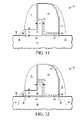
- FIG. 1illustrates, in cross-section, a partially completed NVM device 10 .
- an insulating layer 14is grown on a semiconductor substrate 12 .
- insulating layer 14is a gate dielectric layer comprising a conventional, thermally formed silicon dioxide or silicon oxynitride with a thickness of preferably less than 10 nanometers.
- gate dielectric 14may comprise an alternative gate material such as a first or second transition metal oxide or rare earth oxide material.
- Such alternative gate dielectric materialsare suitable for their high dielectric constant (K), which enables the use of a thicker gate dielectric layer without adversely affecting the electrical and capacitive characteristics of the film.
- Kdielectric constant
- One preferred high K gate dielectricis hafnium oxide (HfO 2 ).
- suitable transition metal oxide compositesselected from oxides of zirconium, hafnium, aluminum, lanthanum, strontium, tantalum, titanium, silicon and the combinations thereof may be used.
- Transition metal silicates and aluminatesmay also be used for the gate dielectric, such as hafnium silicate (Hf x Si y O z ) hafnium aluminate (Hf x Al y O z ).
- a polysilicon layer 16is formed over insulating layer 14 . Polysilicon layer 16 and insulating layer 14 are etched using a conventional etch process to form a select gate for NVM device 10 .
- Polysilicon layer 16is a polysilicon layer or a polysilicon-germanium layer which is either in-situ doped or subsequently doped to be sufficiently conductive for, e.g., a gate electrode application.
- a photoresist layeris formed over polysilicon layer 16 (not shown) and then etched to form a patterned photoresist layer (not shown).
- Polysilicon layer 16is then etched in the areas not covered by the photoresist to form the select gate for NVM device 10 .
- polysilicon layer 16may be from 60 to 200 nanometers thick.
- FIG. 2illustrates, in cross-section, partially completed NVM device 10 .
- a charge storage layer 18is formed over select gate 16 and substrate 12 .
- nanocrystals 19represented by the small circles in charge storage layer 18 , are used to form a plurality of discrete charge storage elements. These nanocrystals are typically formed of silicon, but the discrete storage elements may also be formed of clusters of material consisting of, for example, of germanium, silicon carbide, any number of metals, or in any combination.
- the charge storage materialmay consist of nitride, although any number of dielectrics containing traps may be used, such as aluminum oxide, zirconium oxide, hafnium oxide, tantalum oxide, lanthanum oxide, hafnium silicate, or hafnium aluminate.
- charge storage layer 18may be formed from a different material, such as for example, a floating gate formed from polysilicon.
- a second polysilicon layer 20is deposited over charge storage layer 18 and doped using ion implantation as appropriate for a gate electrode application.
- polysilicon layer 20may be from 40 to 200 nanometers thick.
- FIG. 3illustrates, in cross-section, partially completed NVM device 10 after polysilicon layer 20 and charge storage layer 18 are patterned using a first etching step to form a control gate.
- a photoresist layer(not shown) is formed and patterned.
- polysilicon layer 20is etched in areas not covered by the photoresist layer. Note the over-lap of the control gate polysilicon 20 and select gate polysilicon 16 .
- FIG. 4illustrates, in cross-section, partially completed NVM device 10 after a second etching step is used to form an L-shape in the select gate 16 .
- a second etching stepis used to form an L-shape in the select gate 16 .
- not all of polysilicon layer 16is removed from the uncovered areas.
- the etching processis stopped when polysilicon layer 16 has a reduced thickness in the areas not covered by photo resist layer 24 .
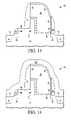
- FIG. 5illustrates, in cross-section, partially completed NVM device 10 after a patterning step to establish a control gate length and select gate length.
- the control gate lengthis in the range of 50-250 nanometers and the select gate length is in the range of 50-250 nanometers.
- the dimension “A” in FIG. 5may be in the range of 10-60 nanometers and the dimension “B” may be in the range of 60-100 nanometers. In another embodiment, the dimension B may be less than 60 nanometers.
- a channel lengthis equal to about the combination of the control gate length, the thickness of the charge storage layer 18 , and the select gate length.
- Device 10can be characterized as being a split-gate NVM cell.
- the split-gate NVM celltypically exhibits two distinguishable channel regions, respectively controllable by the select gate and the control gate.
- FIG. 6illustrates, in cross-section, partially completed NVM device 10 , where an oxide liner 22 is formed over the structure of NVM device 10 , and sidewall spacers 24 , 26 , and 28 are formed over liner 22 .
- spacers 24 , 26 , and 28Prior to forming spacers 24 , 26 , and 28 , source/drain extensions are formed in substrate 12 .
- the spacer materialis typically nitride, although it may be formed of another material that can be selectively etched.
- Spacer 24is formed adjacent to the vertical side of the reduced thickness portion of select gate 16 .
- Spacer 26is formed on the horizontal leg of select gate 16 and adjacent to the vertical leg of the L-shaped select gate 16 and control gate 20 .
- Spacer 28is formed adjacent to control gate 20 on a side opposite the select gate.
- Source/drain regions 30 and 32are then implanted with a relatively low-energy implant, and device 10 is annealed.
- a thickness, dimension B of device 10is sufficiently thick to have an implant blocking capability to prevent implant penetration directly through the horizontal leg during source/drain implantation.
- FIG. 7illustrates, in cross-section, partially completed NVM device 10 , where silicided portions 33 , 34 , 36 , and 38 are formed.
- Silicided portionsare formed by depositing a metal such as cobalt, nickel, platinum, or a combination of metals, on the polysilicon and annealing the device.
- Silicided portions 33 and 38are at a top surface of source/drain regions 30 and 32 , respectively.
- Silicided portion 34is at a top surface of the horizontal leg of L-shaped select gate 16 .
- Silicided portion 36is at a top surface of control gate 20 .
- silicide portion 34may be blocked from the active region, and only formed in a select gate pad region.
- the silicide portion 36may be formed only in a control gate pad region. This is done to make it feasible to use very thin polysilicon gates, that is, polysilicon gates that are less than about 30 nanometers, where silicide may spike through to the gate oxide.
- forming silicide portions 34 and/or 36 only in the gate pad regionsmay be accomplished by using a modified resistor protect oxide (RPO) mask pattern.
- RPOresistor protect oxide
- FIG. 8illustrates, in cross-section, NVM device 10 after a stressor layer 40 is deposited over the device 10 .
- stressor layer 40is a tensile nitride etch stop layer. Stressor layer 40 imparts a longitudinal tensile stress along the channel direction and a vertical compressive stress perpendicular to the channel direction. The stresses are applied to the charge storage layer under the control gate and in the channel region under the control gate.
- FIGS. 9-14illustrate, in cross-section, steps for the fabrication of NVM device 50 in accordance with another embodiment. Unlike the embodiment of FIGS. 1-8 , the embodiment of FIGS. 9-14 uses disposable sidewall spacers.
- FIG. 9illustrates a cross section of partially complete device 50 having a semiconductor substrate 52 , a gate dielectric layer 54 , L-shaped selected gate 56 , charge storage layer 58 and control gate 60 .
- Charge storage layer 58includes nanocrystals 59 .
- Device 50 of FIG. 9may be fabricated by following the steps detailed above in FIGS. 1-5 except that the dimensions A and B are changed to dimensions C and D.
- Dimension “C” of L-shaped select gate 56is in a range of between 10-60 nanometers.
- Dimension “D” of L-shaped select gate 56is in a range of between 20-100 nanometers. In the interest of brevity and clarity the steps of FIG. 1 through FIG. 5 will not be described again.
- FIG. 10illustrates, in cross-section, partially completed NVM device 50 after source/drain extensions 64 and 66 are implanted and oxide liner 62 is deposited.
- FIG. 11illustrates, in cross-section, partially completed NVM device 50 following the deposition of sidewall spacers 68 , 70 , and 72 .
- the spacer materialis nitride, although it may be formed of another material that can be selectively etched.
- Spacer 68is formed on the vertical side of the reduced thickness of select gate 56 .
- Spacer 70is formed on the horizontal leg of select gate 56 and adjacent to the vertical leg of the L-shaped select gate 56 and the vertical edge of control gate 60 as illustrated in FIG. 11 . Spacer 70 spans the horizontal leg of select gate 56 .
- Spacer 72is formed adjacent to and on control gate 60 on a side opposite of select gate 56 .
- FIG. 12illustrates, in cross-section, partially completed NVM device 50 after source/drain region 74 and source/drain region 76 are implanted using ion implantation. Note that source/drain region 74 and source/drain region 76 can be relatively deeper than those of the embodiment illustrated in FIG. 6 because the substantially wider spacer 70 on select gate 56 in FIG. 12 covers, or masks, the whole horizontal leg of the select gate and blocks source/drain implant penetration.
- FIG. 13illustrates, in cross-section, partially completed NVM device 50 after silicide formation.
- spacers 68 , 70 , and 72are removed, new sidewall spacers 78 , 80 , and 82 are formed.
- the spacer materialis titanium nitride, although it may be formed of silicon nitride or another material that can be selectively etched.
- Liner 62is then removed from the areas not covered by spacers 78 , 80 , and 82 .
- Silicided regions 84 , 86 , 88 , and 90are formed. As illustrated in FIG.
- silicided region 84is formed in source/drain region 74
- silicided region 86is formed in select gate 56
- silicided region 88is formed in control gate 60
- silicided region 90is formed in source/drain region 76 .
- silicide portion 86may be blocked from the active region, and only formed in a select gate pad region.
- the silicide portion 88may be formed only in a control gate pad region.
- forming silicide portions 86 and/or 88 only in the gate pad regionsmay be accomplished by using a modified RPO mask pattern. Spacers 78 , 80 , and 82 are then removed.
- FIG. 14illustrates, in cross-section, partially completed NVM device 50 after a stressor layer 92 is deposited over device 50 .
- stressor layer 92is a tensile nitride etch stop layer. Stressor layer 92 imparts a longitudinal tensile stress along the channel direction and a vertical compressive stress perpendicular to the channel direction. The stresses are applied to the charge storage layer under the control gate and in the channel region under the control gate. In both illustrated embodiments, the stress reduces the leakage current from the charge storage layer to the channel region. Note that even though tensile stress is applied in the illustrated embodiment, in another embodiment compressive stress may be applied.
- disposable sidewall spacer 70allows the source/drain regions to be more deeply doped by covering the horizontal portion of L-shaped select gate 56 .
- the removal of spacer 80allows the stressor layer 92 to be closer to the portion of the charge storage layer 58 under the control gate
Landscapes
- Engineering & Computer Science (AREA)
- Chemical & Material Sciences (AREA)
- Nanotechnology (AREA)
- Physics & Mathematics (AREA)
- Mathematical Physics (AREA)
- Theoretical Computer Science (AREA)
- Crystallography & Structural Chemistry (AREA)
- Non-Volatile Memory (AREA)
Abstract
Description
- This application is related to Attorney Docket No. MT11252TP, filed on even date, entitled “Method For Making A Stressed Non-Volatile Memory Device”, by Loiko et al., and assigned to the current assignee hereof.
- 1. Field
- This disclosure relates generally to semiconductors, and more specifically, to a stressed semiconductor device method for making.
- 2. Related Art
- Semiconductor non-volatile memories (NVMs), and particularly flash electrically erasable, programmable read-only memories (EEPROMs), are widely used in a range of electronic equipment from computers, to telecommunications hardware, to consumer appliances. The flash EEPROM is encountered in numerous configurations. In particular, a floating-gate NVM cell is characterized by a stacked gate construction in which a floating gate, typically formed from polysilicon, is separated from the substrate by a first (lower) oxide layer and is separated from a polysilicon control gate by a second (upper) oxide layer. No direct electrical connection is made to the floating gate (hence, “floating”).
- In another configuration, a charge storage layer comprising nanocrystals as the charge storage mechanism is used in place of the floating gate. The nanocrystals function as isolated charge storage elements.
- In many prior art non-volatile memory (NVM) devices, the charge storage layer is separated from the channel region by a relatively thin tunnel dielectric layer. There can be a problem of charge leakage from the charge storage layer to the underlying channel. Such charge leakage can lead to degradation of the memory state stored within the device and is therefore undesirable. In order to avoid such charge leakage, the thickness of the tunnel dielectric is often increased. However, a thicker tunnel dielectric requires higher programming and erasing voltages for storing and removing charge from the charge storage layer as the charge carriers must pass through the thicker tunnel dielectric. In many cases, higher programming voltages increase power consumption and may require the implementation of charge pumps in order to increase the supply voltage to meet programming voltage requirements. Such charge pumps consume a significant amount of die area for the integrated circuit and therefore reduce the memory array area efficiency and increase overall costs.
- Therefore, what is needed is a NVM cell that solves the above problems.
- The present invention is illustrated by way of example and is not limited by the accompanying figures, in which like references indicate similar elements. Elements in the figures are illustrated for simplicity and clarity and have not necessarily been drawn to scale.
FIGS. 1-8 illustrate, in cross-section, steps for the fabrication of an NVM device in accordance with an embodiment.FIGS. 9-14 illustrate, in cross-section, steps for the fabrication of an NVM device in accordance with an embodiment.- Generally, there is provided, a split-gate NVM cell having a tensile stressor layer for providing a stress to the charge storage layer and to the channel region under the control gate of a split-gate NVM cell. In the illustrated embodiment, the stressor layer is a nitride etch-stop layer for providing a longitudinal tensile stress along the channel direction and for providing a vertical compressive stress perpendicular to the channel direction. The stresses are applied to the charge storage layer under the control gate and in the channel region under the control gate. The stress changes the energy barrier height between the bottom insulator and the nanocrystals of the charge storage layer gate. The stress may also increase the effective mass in the nanocrystals of the charge storage layer. The higher energy barrier and increased effective mass improve data retention of the nanocrystals by reducing a leakage current from the charge storage layer to the channel region.
- In one aspect, there is provided, a method of making a semiconductor device on a semiconductor layer, comprising: forming a gate dielectric over the semiconductor layer; forming a first layer of gate material over the gate dielectric; etching the first layer of gate material to remove a portion of the first layer of gate material over a first portion of the semiconductor layer and to leave a select gate portion; forming a storage layer over the select gate portion and over the first portion of the semiconductor layer; forming a second layer of gate material over the storage layer; etching the second layer of gate material to remove a first portion of the second layer of gate material over a first portion of the select gate portion; and etching out a portion of the first portion of the select gate portion to leave an L-shaped select gate structure, wherein: the L-shaped select gate structure has a vertical portion and a horizontal portion; the vertical portion has a height and a width; and the horizontal portion has a thickness that is less than the height of the vertical portion. The step of etching out is further characterized by the thickness of the horizontal layer being sufficiently thick to have implant blocking capability sufficient to prevent implants during the step of implanting if the implants are received directly by the horizontal layer. The step of etching out may further comprise removing a portion of the storage layer over the first portion of the select gate structure. The step of etching the second layer may be further characterized as leaving a second portion of the second layer over the vertical portion and a third portion of the second layer over the first portion of the semiconductor layer. The method may further comprise forming a stressor layer over the semiconductor device after the step of etching out. The method may further comprise removing a portion of the horizontal portion of the L-shaped select gate structure to form a select gate comprising the vertical portion and a portion of the horizontal portion prior to the step of forming the stressor layer. The step of etching the second layer of gate material may be further characterized as forming a control gate from the second layer of gate material, the method further comprising implanting to form a first source/drain region in the semiconductor layer adjacent to the select gate and a second source/drain region in the semiconductor layer adjacent to the control gate. The method may further comprise forming a sidewall spacer spanning the portion of the horizontal portion of the select gate to form a mask during at least a portion of the step of implanting. The step of etching out may be further characterized by the thickness of the horizontal portion being less than 60 nanometers. The step of implanting may further include forming sidewall spacers, and the method may further comprise: forming silicide regions at a top surface of the first and second source/drain regions; removing the sidewall spacers; and forming a stressor layer over the select gate, control gate, and first and second source/drain regions. The step of forming the storage layer may be further characterized by the storage layer comprising nanocrystals. The method may further comprise implanting the first layer of gate material with a dopant for use in making the first layer of gate material conductive. The step of etching out is further characterized by the width of the vertical portion being less than 60 nanometers.
- In another aspect, there is provided, a semiconductor device, comprising: a gate dielectric over a semiconductor layer; an L-shaped select gate over the gate dielectric having a horizontal portion having a thickness and a vertical portion having a width and a height, the height greater than the thickness; a control gate having a first portion over the vertical portion, a second portion laterally adjacent the vertical portion, and a third portion over the semiconductor layer; and a storage layer between the control gate and the select gate and between the control gate and the semiconductor layer. The semiconductor device may further comprise a stressor layer laterally adjacent to and over the control gate and laterally adjacent to and over the select gate. The semiconductor device may further comprise: a first source/drain in the semiconductor layer adjacent to the horizontal portion of the select gate; and a second source/drain in the semiconductor layer laterally adjacent to the control gate, wherein the stressor layer is over the first and second source/drains. The thickness of the horizontal portion may be sufficiently thick to be able block source/drain implants. In an alternative embodiment, the thickness of the horizontal portion may be less than 60 nanometers.
- In yet another embodiment, there is provided, a method of making a semiconductor device on a semiconductor layer, comprising: forming a select gate portion over the semiconductor layer; forming a storage layer having a first portion over the select gate portion and a second portion over the semiconductor layer; forming a control gate structure over the storage layer and having a first portion over a first portion of the select gate portion, a second portion laterally adjacent the select gate portion, and a third portion over the semiconductor layer; removing a portion of the select gate portion to provide a select gate comprising a vertical portion under the first portion of the control gate and a horizontal portion extending away from the control gate, wherein the horizontal portion has a thickness less than a height of the vertical portion; and forming an insulating layer that provides a stress to the semiconductor layer under the control gate and the select gate. The method may further comprise: forming a first source/drain and a second source/drain in the semiconductor layer, wherein the first source/drain is adjacent to the select gate and the second source/drain is adjacent to the control gate.
- The semiconductor substrate described herein can be any semiconductor material or combinations of materials, such as gallium arsenide, silicon germanium, silicon-on-insulator (SOI), silicon, monocrystalline silicon, the like, and combinations of the above.
FIGS. 1-8 illustrate, in cross-section, steps for the fabrication of an NVM device in accordance with an embodiment.FIG. 1 illustrates, in cross-section, a partially completedNVM device 10. InFIG. 1 aninsulating layer 14 is grown on asemiconductor substrate 12. In one embodiment,insulating layer 14 is a gate dielectric layer comprising a conventional, thermally formed silicon dioxide or silicon oxynitride with a thickness of preferably less than 10 nanometers. In another embodiment, gate dielectric14 may comprise an alternative gate material such as a first or second transition metal oxide or rare earth oxide material. Such alternative gate dielectric materials are suitable for their high dielectric constant (K), which enables the use of a thicker gate dielectric layer without adversely affecting the electrical and capacitive characteristics of the film. One preferred high K gate dielectric is hafnium oxide (HfO2). For these alternative gate dielectrics, suitable transition metal oxide composites selected from oxides of zirconium, hafnium, aluminum, lanthanum, strontium, tantalum, titanium, silicon and the combinations thereof may be used. Transition metal silicates and aluminates may also be used for the gate dielectric, such as hafnium silicate (HfxSiyOz) hafnium aluminate (HfxAlyOz). Apolysilicon layer 16 is formed over insulatinglayer 14.Polysilicon layer 16 and insulatinglayer 14 are etched using a conventional etch process to form a select gate forNVM device 10.Polysilicon layer 16 is a polysilicon layer or a polysilicon-germanium layer which is either in-situ doped or subsequently doped to be sufficiently conductive for, e.g., a gate electrode application. A photoresist layer is formed over polysilicon layer16 (not shown) and then etched to form a patterned photoresist layer (not shown).Polysilicon layer 16 is then etched in the areas not covered by the photoresist to form the select gate forNVM device 10. In one embodiment,polysilicon layer 16 may be from 60 to 200 nanometers thick.FIG. 2 illustrates, in cross-section, partially completedNVM device 10. InFIG. 2 , acharge storage layer 18 is formed overselect gate 16 andsubstrate 12. In one embodiment, nanocrystals19, represented by the small circles incharge storage layer 18, are used to form a plurality of discrete charge storage elements. These nanocrystals are typically formed of silicon, but the discrete storage elements may also be formed of clusters of material consisting of, for example, of germanium, silicon carbide, any number of metals, or in any combination. Alternately, the charge storage material may consist of nitride, although any number of dielectrics containing traps may be used, such as aluminum oxide, zirconium oxide, hafnium oxide, tantalum oxide, lanthanum oxide, hafnium silicate, or hafnium aluminate. In another embodiment,charge storage layer 18 may be formed from a different material, such as for example, a floating gate formed from polysilicon. Asecond polysilicon layer 20 is deposited overcharge storage layer 18 and doped using ion implantation as appropriate for a gate electrode application. In one embodiment,polysilicon layer 20 may be from 40 to 200 nanometers thick.FIG. 3 illustrates, in cross-section, partially completedNVM device 10 afterpolysilicon layer 20 andcharge storage layer 18 are patterned using a first etching step to form a control gate. A photoresist layer (not shown) is formed and patterned. Thenpolysilicon layer 20 is etched in areas not covered by the photoresist layer. Note the over-lap of thecontrol gate polysilicon 20 andselect gate polysilicon 16.FIG. 4 illustrates, in cross-section, partially completedNVM device 10 after a second etching step is used to form an L-shape in theselect gate 16. As can be seen inFIG. 4 , not all ofpolysilicon layer 16 is removed from the uncovered areas. In one embodiment, the etching process is stopped whenpolysilicon layer 16 has a reduced thickness in the areas not covered by photo resistlayer 24.FIG. 5 illustrates, in cross-section, partially completedNVM device 10 after a patterning step to establish a control gate length and select gate length. The control gate length is in the range of 50-250 nanometers and the select gate length is in the range of 50-250 nanometers. In one embodiment, the dimension “A” inFIG. 5 may be in the range of 10-60 nanometers and the dimension “B” may be in the range of 60-100 nanometers. In another embodiment, the dimension B may be less than 60 nanometers. A channel length is equal to about the combination of the control gate length, the thickness of thecharge storage layer 18, and the select gate length.Device 10 can be characterized as being a split-gate NVM cell. The split-gate NVM cell typically exhibits two distinguishable channel regions, respectively controllable by the select gate and the control gate.FIG. 6 illustrates, in cross-section, partially completedNVM device 10, where anoxide liner 22 is formed over the structure ofNVM device 10, andsidewall spacers liner 22. Prior to formingspacers substrate 12. The spacer material is typically nitride, although it may be formed of another material that can be selectively etched.Spacer 24 is formed adjacent to the vertical side of the reduced thickness portion ofselect gate 16.Spacer 26 is formed on the horizontal leg ofselect gate 16 and adjacent to the vertical leg of the L-shapedselect gate 16 andcontrol gate 20.Spacer 28 is formed adjacent to controlgate 20 on a side opposite the select gate. Source/drain regions device 10 is annealed. In another embodiment, a thickness, dimension B ofdevice 10, is sufficiently thick to have an implant blocking capability to prevent implant penetration directly through the horizontal leg during source/drain implantation.FIG. 7 illustrates, in cross-section, partially completedNVM device 10, wheresilicided portions Silicided portions drain regions Silicided portion 34 is at a top surface of the horizontal leg of L-shapedselect gate 16.Silicided portion 36 is at a top surface ofcontrol gate 20. Alternatively,silicide portion 34 may be blocked from the active region, and only formed in a select gate pad region. Similarly, thesilicide portion 36 may be formed only in a control gate pad region. This is done to make it feasible to use very thin polysilicon gates, that is, polysilicon gates that are less than about 30 nanometers, where silicide may spike through to the gate oxide. In one embodiment, formingsilicide portions 34 and/or36 only in the gate pad regions may be accomplished by using a modified resistor protect oxide (RPO) mask pattern.FIG. 8 illustrates, in cross-section,NVM device 10 after astressor layer 40 is deposited over thedevice 10. In one embodiment,stressor layer 40 is a tensile nitride etch stop layer.Stressor layer 40 imparts a longitudinal tensile stress along the channel direction and a vertical compressive stress perpendicular to the channel direction. The stresses are applied to the charge storage layer under the control gate and in the channel region under the control gate.FIGS. 9-14 illustrate, in cross-section, steps for the fabrication ofNVM device 50 in accordance with another embodiment. Unlike the embodiment ofFIGS. 1-8 , the embodiment ofFIGS. 9-14 uses disposable sidewall spacers.FIG. 9 illustrates a cross section of partiallycomplete device 50 having asemiconductor substrate 52, agate dielectric layer 54, L-shaped selectedgate 56,charge storage layer 58 andcontrol gate 60.Charge storage layer 58 includesnanocrystals 59.Device 50 ofFIG. 9 may be fabricated by following the steps detailed above inFIGS. 1-5 except that the dimensions A and B are changed to dimensions C and D. Dimension “C” of L-shapedselect gate 56 is in a range of between 10-60 nanometers. Dimension “D” of L-shapedselect gate 56 is in a range of between 20-100 nanometers. In the interest of brevity and clarity the steps ofFIG. 1 throughFIG. 5 will not be described again.FIG. 10 illustrates, in cross-section, partially completedNVM device 50 after source/drain extensions oxide liner 62 is deposited.FIG. 11 illustrates, in cross-section, partially completedNVM device 50 following the deposition ofsidewall spacers Spacer 68 is formed on the vertical side of the reduced thickness ofselect gate 56.Spacer 70 is formed on the horizontal leg ofselect gate 56 and adjacent to the vertical leg of the L-shapedselect gate 56 and the vertical edge ofcontrol gate 60 as illustrated inFIG. 11 .Spacer 70 spans the horizontal leg ofselect gate 56.Spacer 72 is formed adjacent to and oncontrol gate 60 on a side opposite ofselect gate 56.FIG. 12 illustrates, in cross-section, partially completedNVM device 50 after source/drain region 74 and source/drain region 76 are implanted using ion implantation. Note that source/drain region 74 and source/drain region 76 can be relatively deeper than those of the embodiment illustrated inFIG. 6 because the substantiallywider spacer 70 onselect gate 56 inFIG. 12 covers, or masks, the whole horizontal leg of the select gate and blocks source/drain implant penetration.FIG. 13 illustrates, in cross-section, partially completedNVM device 50 after silicide formation. After spacers68,70, and72 are removed,new sidewall spacers Liner 62 is then removed from the areas not covered byspacers Silicided regions FIG. 13 ,silicided region 84 is formed in source/drain region 74,silicided region 86 is formed inselect gate 56,silicided region 88 is formed incontrol gate 60, andsilicided region 90 is formed in source/drain region 76. Alternatively,silicide portion 86 may be blocked from the active region, and only formed in a select gate pad region. Similarly, thesilicide portion 88 may be formed only in a control gate pad region. In one embodiment, formingsilicide portions 86 and/or88 only in the gate pad regions may be accomplished by using a modified RPO mask pattern.Spacers FIG. 14 illustrates, in cross-section, partially completedNVM device 50 after astressor layer 92 is deposited overdevice 50. In one embodiment,stressor layer 92 is a tensile nitride etch stop layer.Stressor layer 92 imparts a longitudinal tensile stress along the channel direction and a vertical compressive stress perpendicular to the channel direction. The stresses are applied to the charge storage layer under the control gate and in the channel region under the control gate. In both illustrated embodiments, the stress reduces the leakage current from the charge storage layer to the channel region. Note that even though tensile stress is applied in the illustrated embodiment, in another embodiment compressive stress may be applied. The use ofdisposable sidewall spacer 70 allows the source/drain regions to be more deeply doped by covering the horizontal portion of L-shapedselect gate 56. The removal ofspacer 80 allows thestressor layer 92 to be closer to the portion of thecharge storage layer 58 under the control gate- Moreover, the terms “front,” “back,” “top,” “bottom,” “over,” “under” and the like in the description and in the claims, if any, are used for descriptive purposes and not necessarily for describing permanent relative positions. It is understood that the terms so used are interchangeable under appropriate circumstances such that the embodiments of the invention described herein are, for example, capable of operation in other orientations than those illustrated or otherwise described herein.
- Although the invention is described herein with reference to specific embodiments, various modifications and changes can be made without departing from the scope of the present invention as set forth in the claims below. Accordingly, the specification and figures are to be regarded in an illustrative rather than a restrictive sense, and all such modifications are intended to be included within the scope of the present invention. Any benefits, advantages, or solutions to problems that are described herein with regard to specific embodiments are not intended to be construed as a critical, required, or essential feature or element of any or all the claims.
- Furthermore, the terms “a” or “an,” as used herein, are defined as one or more than one. Also, the use of introductory phrases such as “at least one” and “one or more” in the claims should not be construed to imply that the introduction of another claim element by the indefinite articles “a” or “an” limits any particular claim containing such introduced claim element to inventions containing only one such element, even when the same claim includes the introductory phrases “one or more” or “at least one” and indefinite articles such as “a” or “an.” The same holds true for the use of definite articles.
- Unless stated otherwise, terms such as “first” and “second” are used to arbitrarily distinguish between the elements such terms describe. Thus, these terms are not necessarily intended to indicate temporal or other prioritization of such elements.
Claims (20)
Priority Applications (1)
| Application Number | Priority Date | Filing Date | Title |
|---|---|---|---|
| US12/414,763US7821055B2 (en) | 2009-03-31 | 2009-03-31 | Stressed semiconductor device and method for making |
Applications Claiming Priority (1)
| Application Number | Priority Date | Filing Date | Title |
|---|---|---|---|
| US12/414,763US7821055B2 (en) | 2009-03-31 | 2009-03-31 | Stressed semiconductor device and method for making |
Publications (2)
| Publication Number | Publication Date |
|---|---|
| US20100244121A1true US20100244121A1 (en) | 2010-09-30 |
| US7821055B2 US7821055B2 (en) | 2010-10-26 |
Family
ID=42783034
Family Applications (1)
| Application Number | Title | Priority Date | Filing Date |
|---|---|---|---|
| US12/414,763ActiveUS7821055B2 (en) | 2009-03-31 | 2009-03-31 | Stressed semiconductor device and method for making |
Country Status (1)
| Country | Link |
|---|---|
| US (1) | US7821055B2 (en) |
Cited By (7)
| Publication number | Priority date | Publication date | Assignee | Title |
|---|---|---|---|---|
| CN102800695A (en)* | 2011-05-24 | 2012-11-28 | 爱思开海力士有限公司 | 3-dimensional non-volatile memory device and method of manufacturing the same |
| US8530950B1 (en)* | 2012-05-31 | 2013-09-10 | Freescale Semiconductor, Inc. | Methods and structures for split gate memory |
| US8853027B2 (en) | 2012-10-01 | 2014-10-07 | Freescale Semiconductor, Inc. | Split gate flash cell |
| US20150001606A1 (en)* | 2013-06-28 | 2015-01-01 | Cheong Min Hong | Methods and structures for a split gate memory cell structure |
| US9257445B2 (en)* | 2014-05-30 | 2016-02-09 | Freescale Semiconductor, Inc. | Method of making a split gate non-volatile memory (NVM) cell and a logic transistor |
| US9761689B2 (en)* | 2014-09-12 | 2017-09-12 | Globalfoundries Inc. | Method of forming a semiconductor device and according semiconductor device |
| US20200027996A1 (en)* | 2018-07-17 | 2020-01-23 | Renesas Electronics Corporation | Semiconductor device and a method of manufacturing the same |
Families Citing this family (30)
| Publication number | Priority date | Publication date | Assignee | Title |
|---|---|---|---|---|
| US8399310B2 (en) | 2010-10-29 | 2013-03-19 | Freescale Semiconductor, Inc. | Non-volatile memory and logic circuit process integration |
| US8669609B2 (en)* | 2011-02-28 | 2014-03-11 | Freescale Semiconductor, Inc. | Non-volatile memory (NVM) cell for endurance and method of making |
| US9202930B2 (en) | 2011-05-19 | 2015-12-01 | Freescale Semiconductor, Inc. | Memory with discrete storage elements |
| US8906764B2 (en) | 2012-01-04 | 2014-12-09 | Freescale Semiconductor, Inc. | Non-volatile memory (NVM) and logic integration |
| US8951863B2 (en) | 2012-04-06 | 2015-02-10 | Freescale Semiconductor, Inc. | Non-volatile memory (NVM) and logic integration |
| US9087913B2 (en) | 2012-04-09 | 2015-07-21 | Freescale Semiconductor, Inc. | Integration technique using thermal oxide select gate dielectric for select gate and apartial replacement gate for logic |
| US9165652B2 (en)* | 2012-08-20 | 2015-10-20 | Freescale Semiconductor, Inc. | Split-gate memory cells having select-gate sidewall metal silicide regions and related manufacturing methods |
| US9111865B2 (en) | 2012-10-26 | 2015-08-18 | Freescale Semiconductor, Inc. | Method of making a logic transistor and a non-volatile memory (NVM) cell |
| US9006093B2 (en) | 2013-06-27 | 2015-04-14 | Freescale Semiconductor, Inc. | Non-volatile memory (NVM) and high voltage transistor integration |
| US9129996B2 (en) | 2013-07-31 | 2015-09-08 | Freescale Semiconductor, Inc. | Non-volatile memory (NVM) cell and high-K and metal gate transistor integration |
| US8877585B1 (en) | 2013-08-16 | 2014-11-04 | Freescale Semiconductor, Inc. | Non-volatile memory (NVM) cell, high voltage transistor, and high-K and metal gate transistor integration |
| US8871598B1 (en) | 2013-07-31 | 2014-10-28 | Freescale Semiconductor, Inc. | Non-volatile memory (NVM) and high-k and metal gate integration using gate-first methodology |
| US9082837B2 (en) | 2013-08-08 | 2015-07-14 | Freescale Semiconductor, Inc. | Nonvolatile memory bitcell with inlaid high k metal select gate |
| US9082650B2 (en) | 2013-08-21 | 2015-07-14 | Freescale Semiconductor, Inc. | Integrated split gate non-volatile memory cell and logic structure |
| US9252246B2 (en) | 2013-08-21 | 2016-02-02 | Freescale Semiconductor, Inc. | Integrated split gate non-volatile memory cell and logic device |
| US9275864B2 (en) | 2013-08-22 | 2016-03-01 | Freescale Semiconductor,Inc. | Method to form a polysilicon nanocrystal thin film storage bitcell within a high k metal gate platform technology using a gate last process to form transistor gates |
| US8932925B1 (en) | 2013-08-22 | 2015-01-13 | Freescale Semiconductor, Inc. | Split-gate non-volatile memory (NVM) cell and device structure integration |
| US8901632B1 (en) | 2013-09-30 | 2014-12-02 | Freescale Semiconductor, Inc. | Non-volatile memory (NVM) and high-K and metal gate integration using gate-last methodology |
| US9129855B2 (en) | 2013-09-30 | 2015-09-08 | Freescale Semiconductor, Inc. | Non-volatile memory (NVM) and high-k and metal gate integration using gate-first methodology |
| US9136129B2 (en) | 2013-09-30 | 2015-09-15 | Freescale Semiconductor, Inc. | Non-volatile memory (NVM) and high-k and metal gate integration using gate-last methodology |
| US9231077B2 (en) | 2014-03-03 | 2016-01-05 | Freescale Semiconductor, Inc. | Method of making a logic transistor and non-volatile memory (NVM) cell |
| US9472418B2 (en) | 2014-03-28 | 2016-10-18 | Freescale Semiconductor, Inc. | Method for forming a split-gate device |
| US9112056B1 (en) | 2014-03-28 | 2015-08-18 | Freescale Semiconductor, Inc. | Method for forming a split-gate device |
| US9252152B2 (en) | 2014-03-28 | 2016-02-02 | Freescale Semiconductor, Inc. | Method for forming a split-gate device |
| US9379222B2 (en) | 2014-05-30 | 2016-06-28 | Freescale Semiconductor, Inc. | Method of making a split gate non-volatile memory (NVM) cell |
| US9343314B2 (en) | 2014-05-30 | 2016-05-17 | Freescale Semiconductor, Inc. | Split gate nanocrystal memory integration |
| US9653164B2 (en)* | 2015-03-13 | 2017-05-16 | Nxp Usa, Inc. | Method for integrating non-volatile memory cells with static random access memory cells and logic transistors |
| US9437500B1 (en) | 2015-03-13 | 2016-09-06 | Freescale Semiconductor, Inc. | Method of forming supra low threshold devices |
| DE102018107908B4 (en) | 2017-07-28 | 2023-01-05 | Taiwan Semiconductor Manufacturing Co., Ltd. | Method of forming an integrated circuit with a sealing layer for forming a memory cell structure in logic or BCD technology, and an integrated circuit with a dummy structure at a boundary of a device region |
| US10504912B2 (en)* | 2017-07-28 | 2019-12-10 | Taiwan Semiconductor Manufacturing Co., Ltd. | Seal method to integrate non-volatile memory (NVM) into logic or bipolar CMOS DMOS (BCD) technology |
Citations (11)
| Publication number | Priority date | Publication date | Assignee | Title |
|---|---|---|---|---|
| US5408115A (en)* | 1994-04-04 | 1995-04-18 | Motorola Inc. | Self-aligned, split-gate EEPROM device |
| US6875660B2 (en)* | 2003-02-26 | 2005-04-05 | Powerchip Semiconductor Corp. | Method of manufacturing high coupling ratio flash memory having sidewall spacer floating gate electrode |
| US20050104115A1 (en)* | 2002-04-01 | 2005-05-19 | Sohrab Kianian | Self aligned method of forming a semiconductor memory array of floating gate memory cells with buried bit-line and raised source line, and a memory array made thereby |
| US20070132054A1 (en)* | 2005-12-13 | 2007-06-14 | Applied Materials | Memory cell having stressed layers |
| US7235441B2 (en)* | 2003-10-20 | 2007-06-26 | Renesas Technology Corp. | Nonvolatile semiconductor memory device with tapered sidewall gate and method of manufacturing the same |
| US20080042183A1 (en)* | 2006-08-16 | 2008-02-21 | Nima Mokhlesi | Nonvolatile Memories with Shaped Floating Gates |
| US7436019B2 (en)* | 2004-03-12 | 2008-10-14 | Sandisk Corporation | Non-volatile memory cells shaped to increase coupling to word lines |
| US20080261385A1 (en)* | 2007-04-20 | 2008-10-23 | Dharmesh Jawarani | Method for selective removal of a layer |
| US7446370B2 (en)* | 2006-04-20 | 2008-11-04 | Powerchip Semiconductor Corp. | Non-volatile memory |
| US7494860B2 (en)* | 2006-08-16 | 2009-02-24 | Sandisk Corporation | Methods of forming nonvolatile memories with L-shaped floating gates |
| US7557402B2 (en)* | 2004-06-17 | 2009-07-07 | Taiwan Semiconductor Manufacturing Company, Ltd. | High write and erase efficiency embedded flash cell |
- 2009
- 2009-03-31USUS12/414,763patent/US7821055B2/enactiveActive
Patent Citations (12)
| Publication number | Priority date | Publication date | Assignee | Title |
|---|---|---|---|---|
| US5408115A (en)* | 1994-04-04 | 1995-04-18 | Motorola Inc. | Self-aligned, split-gate EEPROM device |
| US20050104115A1 (en)* | 2002-04-01 | 2005-05-19 | Sohrab Kianian | Self aligned method of forming a semiconductor memory array of floating gate memory cells with buried bit-line and raised source line, and a memory array made thereby |
| US6875660B2 (en)* | 2003-02-26 | 2005-04-05 | Powerchip Semiconductor Corp. | Method of manufacturing high coupling ratio flash memory having sidewall spacer floating gate electrode |
| US7235441B2 (en)* | 2003-10-20 | 2007-06-26 | Renesas Technology Corp. | Nonvolatile semiconductor memory device with tapered sidewall gate and method of manufacturing the same |
| US7436019B2 (en)* | 2004-03-12 | 2008-10-14 | Sandisk Corporation | Non-volatile memory cells shaped to increase coupling to word lines |
| US7557402B2 (en)* | 2004-06-17 | 2009-07-07 | Taiwan Semiconductor Manufacturing Company, Ltd. | High write and erase efficiency embedded flash cell |
| US20070132054A1 (en)* | 2005-12-13 | 2007-06-14 | Applied Materials | Memory cell having stressed layers |
| US7446370B2 (en)* | 2006-04-20 | 2008-11-04 | Powerchip Semiconductor Corp. | Non-volatile memory |
| US20090004796A1 (en)* | 2006-04-20 | 2009-01-01 | Powerchip Semiconductor Corp. | Method of manufacturing non-volatile memory |
| US20080042183A1 (en)* | 2006-08-16 | 2008-02-21 | Nima Mokhlesi | Nonvolatile Memories with Shaped Floating Gates |
| US7494860B2 (en)* | 2006-08-16 | 2009-02-24 | Sandisk Corporation | Methods of forming nonvolatile memories with L-shaped floating gates |
| US20080261385A1 (en)* | 2007-04-20 | 2008-10-23 | Dharmesh Jawarani | Method for selective removal of a layer |
Cited By (13)
| Publication number | Priority date | Publication date | Assignee | Title |
|---|---|---|---|---|
| US9559114B2 (en)* | 2011-05-24 | 2017-01-31 | SK Hynix Inc. | Manufacturing method of three-dimensional non-volatile memory device including a selection gate having an L shape |
| US20140242765A1 (en)* | 2011-05-24 | 2014-08-28 | SK Hynix Inc. | 3-dimensional non-volatile memory device including a selection gate having an l shape |
| CN102800695A (en)* | 2011-05-24 | 2012-11-28 | 爱思开海力士有限公司 | 3-dimensional non-volatile memory device and method of manufacturing the same |
| US8530950B1 (en)* | 2012-05-31 | 2013-09-10 | Freescale Semiconductor, Inc. | Methods and structures for split gate memory |
| US8853027B2 (en) | 2012-10-01 | 2014-10-07 | Freescale Semiconductor, Inc. | Split gate flash cell |
| US20150001606A1 (en)* | 2013-06-28 | 2015-01-01 | Cheong Min Hong | Methods and structures for a split gate memory cell structure |
| US9590058B2 (en)* | 2013-06-28 | 2017-03-07 | Nxp Usa, Inc. | Methods and structures for a split gate memory cell structure |
| US20170194444A1 (en)* | 2013-06-28 | 2017-07-06 | Nxp Usa, Inc. | Methods and structures for a split gate memory cell structure |
| US10153349B2 (en)* | 2013-06-28 | 2018-12-11 | Nxp Usa, Inc. | Methods and structures for a split gate memory cell structure |
| US9257445B2 (en)* | 2014-05-30 | 2016-02-09 | Freescale Semiconductor, Inc. | Method of making a split gate non-volatile memory (NVM) cell and a logic transistor |
| US9761689B2 (en)* | 2014-09-12 | 2017-09-12 | Globalfoundries Inc. | Method of forming a semiconductor device and according semiconductor device |
| US20200027996A1 (en)* | 2018-07-17 | 2020-01-23 | Renesas Electronics Corporation | Semiconductor device and a method of manufacturing the same |
| US11094833B2 (en)* | 2018-07-17 | 2021-08-17 | Renesas Electronics Corporation | Semiconductor device including memory using hafnium and a method of manufacturing the same |
Also Published As
| Publication number | Publication date |
|---|---|
| US7821055B2 (en) | 2010-10-26 |
Similar Documents
| Publication | Publication Date | Title |
|---|---|---|
| US7821055B2 (en) | Stressed semiconductor device and method for making | |
| US8557658B2 (en) | Multi-transistor non-volatile memory element | |
| US7811889B2 (en) | FinFET memory cell having a floating gate and method therefor | |
| US8263463B2 (en) | Nonvolatile split gate memory cell having oxide growth | |
| US7427533B2 (en) | Methods of fabricating semiconductor devices including trench device isolation layers having protective insulating layers and related devices | |
| US11968828B2 (en) | Method of forming a semiconductor device with a dual gate dielectric layer having middle portion thinner than the edge portions | |
| US8283716B2 (en) | High performance flash memory devices | |
| US7192830B2 (en) | Method for fabricating a memory cell | |
| WO2007122567A1 (en) | Non-volatile memory device | |
| US20060202254A1 (en) | Multi-level flash memory cell capable of fast programming | |
| JP2008530771A (en) | Electrically rewritable non-volatile memory cell for storing multiple data and manufacturing method thereof | |
| US7265409B2 (en) | Non-volatile semiconductor memory | |
| US20220139718A1 (en) | Integrated circuit device | |
| CN1323439C (en) | Permanent memory cell employing a plurality of dielectric nanoclusters and method of manufacturing the same | |
| US9418864B2 (en) | Method of forming a non volatile memory device using wet etching | |
| US20080182375A1 (en) | Split gate memory cell method | |
| US20100264481A1 (en) | Nonvolatile Memory Devices and Related Methods | |
| KR20060035551A (en) | Nonvolatile Memory Device and Manufacturing Method Thereof | |
| US6869843B2 (en) | Non-volatile memory cell with dielectric spacers along sidewalls of a component stack, and method for forming same | |
| US7408219B2 (en) | Nonvolatile semiconductor memory device | |
| US7541639B2 (en) | Memory device and method of fabricating the same | |
| US7579239B2 (en) | Method for the manufacture of a non-volatile memory device and memory device thus obtained | |
| KR100567350B1 (en) | Method for fabricating non-volatile memory device | |
| US20110084327A1 (en) | 3-d electrically programmable and erasable single-transistor non-volatile semiconductor memory device | |
| KR100874434B1 (en) | Manufacturing method of nonvolatile memory device |
Legal Events
| Date | Code | Title | Description |
|---|---|---|---|
| AS | Assignment | Owner name:FREESCALE SEMICONDUCTOR, INC., TEXAS Free format text:ASSIGNMENT OF ASSIGNORS INTEREST;ASSIGNORS:LOIKO, KONSTANTIN V.;HONG, CHEONG M.;KANG, SUNG-TAEG;AND OTHERS;SIGNING DATES FROM 20090305 TO 20090325;REEL/FRAME:022475/0634 | |
| AS | Assignment | Owner name:CITIBANK, N.A., NEW YORK Free format text:SECURITY AGREEMENT;ASSIGNOR:FREESCALE SEMICONDUCTOR, INC.;REEL/FRAME:022703/0405 Effective date:20090428 | |
| STCF | Information on status: patent grant | Free format text:PATENTED CASE | |
| AS | Assignment | Owner name:CITIBANK, N.A., AS NOTES COLLATERAL AGENT, NEW YORK Free format text:SECURITY AGREEMENT;ASSIGNOR:FREESCALE SEMICONDUCTOR, INC.;REEL/FRAME:030633/0424 Effective date:20130521 Owner name:CITIBANK, N.A., AS NOTES COLLATERAL AGENT, NEW YOR Free format text:SECURITY AGREEMENT;ASSIGNOR:FREESCALE SEMICONDUCTOR, INC.;REEL/FRAME:030633/0424 Effective date:20130521 | |
| AS | Assignment | Owner name:CITIBANK, N.A., AS NOTES COLLATERAL AGENT, NEW YORK Free format text:SECURITY AGREEMENT;ASSIGNOR:FREESCALE SEMICONDUCTOR, INC.;REEL/FRAME:031591/0266 Effective date:20131101 Owner name:CITIBANK, N.A., AS NOTES COLLATERAL AGENT, NEW YOR Free format text:SECURITY AGREEMENT;ASSIGNOR:FREESCALE SEMICONDUCTOR, INC.;REEL/FRAME:031591/0266 Effective date:20131101 | |
| FPAY | Fee payment | Year of fee payment:4 | |
| AS | Assignment | Owner name:FREESCALE SEMICONDUCTOR, INC., TEXAS Free format text:PATENT RELEASE;ASSIGNOR:CITIBANK, N.A., AS COLLATERAL AGENT;REEL/FRAME:037354/0793 Effective date:20151207 | |
| AS | Assignment | Owner name:MORGAN STANLEY SENIOR FUNDING, INC., MARYLAND Free format text:ASSIGNMENT AND ASSUMPTION OF SECURITY INTEREST IN PATENTS;ASSIGNOR:CITIBANK, N.A.;REEL/FRAME:037486/0517 Effective date:20151207 | |
| AS | Assignment | Owner name:MORGAN STANLEY SENIOR FUNDING, INC., MARYLAND Free format text:ASSIGNMENT AND ASSUMPTION OF SECURITY INTEREST IN PATENTS;ASSIGNOR:CITIBANK, N.A.;REEL/FRAME:037518/0292 Effective date:20151207 | |
| AS | Assignment | Owner name:MORGAN STANLEY SENIOR FUNDING, INC., MARYLAND Free format text:SUPPLEMENT TO THE SECURITY AGREEMENT;ASSIGNOR:FREESCALE SEMICONDUCTOR, INC.;REEL/FRAME:039138/0001 Effective date:20160525 | |
| AS | Assignment | Owner name:NXP, B.V., F/K/A FREESCALE SEMICONDUCTOR, INC., NETHERLANDS Free format text:RELEASE BY SECURED PARTY;ASSIGNOR:MORGAN STANLEY SENIOR FUNDING, INC.;REEL/FRAME:040925/0001 Effective date:20160912 Owner name:NXP, B.V., F/K/A FREESCALE SEMICONDUCTOR, INC., NE Free format text:RELEASE BY SECURED PARTY;ASSIGNOR:MORGAN STANLEY SENIOR FUNDING, INC.;REEL/FRAME:040925/0001 Effective date:20160912 | |
| AS | Assignment | Owner name:NXP B.V., NETHERLANDS Free format text:RELEASE BY SECURED PARTY;ASSIGNOR:MORGAN STANLEY SENIOR FUNDING, INC.;REEL/FRAME:040928/0001 Effective date:20160622 | |
| AS | Assignment | Owner name:NXP USA, INC., TEXAS Free format text:CHANGE OF NAME;ASSIGNOR:FREESCALE SEMICONDUCTOR, INC.;REEL/FRAME:040632/0001 Effective date:20161107 | |
| AS | Assignment | Owner name:MORGAN STANLEY SENIOR FUNDING, INC., MARYLAND Free format text:CORRECTIVE ASSIGNMENT TO CORRECT THE REMOVE PATENTS 8108266 AND 8062324 AND REPLACE THEM WITH 6108266 AND 8060324 PREVIOUSLY RECORDED ON REEL 037518 FRAME 0292. ASSIGNOR(S) HEREBY CONFIRMS THE ASSIGNMENT AND ASSUMPTION OF SECURITY INTEREST IN PATENTS;ASSIGNOR:CITIBANK, N.A.;REEL/FRAME:041703/0536 Effective date:20151207 | |
| AS | Assignment | Owner name:NXP USA, INC., TEXAS Free format text:CORRECTIVE ASSIGNMENT TO CORRECT THE NATURE OF CONVEYANCE PREVIOUSLY RECORDED AT REEL: 040632 FRAME: 0001. ASSIGNOR(S) HEREBY CONFIRMS THE MERGER AND CHANGE OF NAME;ASSIGNOR:FREESCALE SEMICONDUCTOR INC.;REEL/FRAME:044209/0047 Effective date:20161107 | |
| MAFP | Maintenance fee payment | Free format text:PAYMENT OF MAINTENANCE FEE, 8TH YEAR, LARGE ENTITY (ORIGINAL EVENT CODE: M1552) Year of fee payment:8 | |
| AS | Assignment | Owner name:SHENZHEN XINGUODU TECHNOLOGY CO., LTD., CHINA Free format text:CORRECTIVE ASSIGNMENT TO CORRECT THE TO CORRECT THE APPLICATION NO. FROM 13,883,290 TO 13,833,290 PREVIOUSLY RECORDED ON REEL 041703 FRAME 0536. ASSIGNOR(S) HEREBY CONFIRMS THE THE ASSIGNMENT AND ASSUMPTION OF SECURITYINTEREST IN PATENTS.;ASSIGNOR:MORGAN STANLEY SENIOR FUNDING, INC.;REEL/FRAME:048734/0001 Effective date:20190217 | |
| AS | Assignment | Owner name:NXP B.V., NETHERLANDS Free format text:RELEASE BY SECURED PARTY;ASSIGNOR:MORGAN STANLEY SENIOR FUNDING, INC.;REEL/FRAME:050744/0097 Effective date:20190903 | |
| AS | Assignment | Owner name:MORGAN STANLEY SENIOR FUNDING, INC., MARYLAND Free format text:CORRECTIVE ASSIGNMENT TO CORRECT THE REMOVE APPLICATION11759915 AND REPLACE IT WITH APPLICATION 11759935 PREVIOUSLY RECORDED ON REEL 037486 FRAME 0517. ASSIGNOR(S) HEREBY CONFIRMS THE ASSIGNMENT AND ASSUMPTION OF SECURITYINTEREST IN PATENTS;ASSIGNOR:CITIBANK, N.A.;REEL/FRAME:053547/0421 Effective date:20151207 | |
| AS | Assignment | Owner name:NXP B.V., NETHERLANDS Free format text:CORRECTIVE ASSIGNMENT TO CORRECT THE REMOVEAPPLICATION 11759915 AND REPLACE IT WITH APPLICATION11759935 PREVIOUSLY RECORDED ON REEL 040928 FRAME 0001. ASSIGNOR(S) HEREBY CONFIRMS THE RELEASE OF SECURITYINTEREST;ASSIGNOR:MORGAN STANLEY SENIOR FUNDING, INC.;REEL/FRAME:052915/0001 Effective date:20160622 | |
| AS | Assignment | Owner name:NXP, B.V. F/K/A FREESCALE SEMICONDUCTOR, INC., NETHERLANDS Free format text:CORRECTIVE ASSIGNMENT TO CORRECT THE REMOVEAPPLICATION 11759915 AND REPLACE IT WITH APPLICATION11759935 PREVIOUSLY RECORDED ON REEL 040925 FRAME 0001. ASSIGNOR(S) HEREBY CONFIRMS THE RELEASE OF SECURITYINTEREST;ASSIGNOR:MORGAN STANLEY SENIOR FUNDING, INC.;REEL/FRAME:052917/0001 Effective date:20160912 | |
| MAFP | Maintenance fee payment | Free format text:PAYMENT OF MAINTENANCE FEE, 12TH YEAR, LARGE ENTITY (ORIGINAL EVENT CODE: M1553); ENTITY STATUS OF PATENT OWNER: LARGE ENTITY Year of fee payment:12 |