US20100232212A1 - Split-gate dram with lateral control-gate mugfet - Google Patents
Split-gate dram with lateral control-gate mugfetDownload PDFInfo
- Publication number
- US20100232212A1 US20100232212A1US12/538,196US53819609AUS2010232212A1US 20100232212 A1US20100232212 A1US 20100232212A1US 53819609 AUS53819609 AUS 53819609AUS 2010232212 A1US2010232212 A1US 2010232212A1
- Authority
- US
- United States
- Prior art keywords
- fin
- gate
- finfet
- split
- storage capacitor
- Prior art date
- Legal status (The legal status is an assumption and is not a legal conclusion. Google has not performed a legal analysis and makes no representation as to the accuracy of the status listed.)
- Granted
Links
- 239000004065semiconductorSubstances0.000claimsabstractdescription23
- 230000005669field effectEffects0.000claimsabstractdescription17
- 239000000758substrateSubstances0.000claimsabstractdescription10
- 238000013461designMethods0.000claimsdescription67
- 239000003990capacitorSubstances0.000claimsdescription35
- 238000003860storageMethods0.000claimsdescription28
- 238000000034methodMethods0.000claimsdescription26
- 238000004519manufacturing processMethods0.000claimsdescription18
- 238000012360testing methodMethods0.000claimsdescription9
- XUIMIQQOPSSXEZ-UHFFFAOYSA-NSiliconChemical group[Si]XUIMIQQOPSSXEZ-UHFFFAOYSA-N0.000description23
- 239000004020conductorSubstances0.000description19
- 238000012545processingMethods0.000description17
- 238000005530etchingMethods0.000description15
- 239000000463materialSubstances0.000description15
- VYPSYNLAJGMNEJ-UHFFFAOYSA-NSilicium dioxideChemical compoundO=[Si]=OVYPSYNLAJGMNEJ-UHFFFAOYSA-N0.000description14
- 238000012938design processMethods0.000description13
- 229910052710siliconInorganic materials0.000description11
- 239000010703siliconSubstances0.000description11
- 230000008569processEffects0.000description10
- 239000012212insulatorSubstances0.000description9
- 239000003989dielectric materialSubstances0.000description8
- 239000007772electrode materialSubstances0.000description8
- 238000000059patterningMethods0.000description8
- 238000004088simulationMethods0.000description8
- 239000000377silicon dioxideSubstances0.000description7
- 229910052681coesiteInorganic materials0.000description6
- 229910052906cristobaliteInorganic materials0.000description6
- 238000001020plasma etchingMethods0.000description6
- 229910052682stishoviteInorganic materials0.000description6
- 229910052905tridymiteInorganic materials0.000description6
- NRTOMJZYCJJWKI-UHFFFAOYSA-NTitanium nitrideChemical compound[Ti]#NNRTOMJZYCJJWKI-UHFFFAOYSA-N0.000description5
- 238000000151depositionMethods0.000description5
- 229910021420polycrystalline siliconInorganic materials0.000description5
- 229920005591polysiliconPolymers0.000description5
- WFKWXMTUELFFGS-UHFFFAOYSA-NtungstenChemical compound[W]WFKWXMTUELFFGS-UHFFFAOYSA-N0.000description5
- 229910052721tungstenInorganic materials0.000description5
- 239000010937tungstenSubstances0.000description5
- 150000004767nitridesChemical class0.000description4
- BPQQTUXANYXVAA-UHFFFAOYSA-NOrthosilicateChemical compound[O-][Si]([O-])([O-])[O-]BPQQTUXANYXVAA-UHFFFAOYSA-N0.000description3
- 229910052581Si3N4Inorganic materials0.000description3
- 238000003491arrayMethods0.000description3
- 230000005540biological transmissionEffects0.000description3
- 229910052735hafniumInorganic materials0.000description3
- VBJZVLUMGGDVMO-UHFFFAOYSA-Nhafnium atomChemical compound[Hf]VBJZVLUMGGDVMO-UHFFFAOYSA-N0.000description3
- 230000000873masking effectEffects0.000description3
- RYGMFSIKBFXOCR-UHFFFAOYSA-NCopperChemical compound[Cu]RYGMFSIKBFXOCR-UHFFFAOYSA-N0.000description2
- 238000004458analytical methodMethods0.000description2
- 238000000231atomic layer depositionMethods0.000description2
- 230000015572biosynthetic processEffects0.000description2
- 239000007795chemical reaction productSubstances0.000description2
- 238000005229chemical vapour depositionMethods0.000description2
- 238000007796conventional methodMethods0.000description2
- 229910052802copperInorganic materials0.000description2
- 239000010949copperSubstances0.000description2
- 238000013500data storageMethods0.000description2
- 230000007423decreaseEffects0.000description2
- 230000008021depositionEffects0.000description2
- 238000010586diagramMethods0.000description2
- 230000000694effectsEffects0.000description2
- 238000005516engineering processMethods0.000description2
- 230000006870functionEffects0.000description2
- 229910000449hafnium oxideInorganic materials0.000description2
- WIHZLLGSGQNAGK-UHFFFAOYSA-Nhafnium(4+);oxygen(2-)Chemical compound[O-2].[O-2].[Hf+4]WIHZLLGSGQNAGK-UHFFFAOYSA-N0.000description2
- 238000002955isolationMethods0.000description2
- 238000012986modificationMethods0.000description2
- 230000004048modificationEffects0.000description2
- 125000006850spacer groupChemical group0.000description2
- 239000000126substanceSubstances0.000description2
- MZLGASXMSKOWSE-UHFFFAOYSA-Ntantalum nitrideChemical compound[Ta]#NMZLGASXMSKOWSE-UHFFFAOYSA-N0.000description2
- 238000012795verificationMethods0.000description2
- 239000004642PolyimideSubstances0.000description1
- 229910052782aluminiumInorganic materials0.000description1
- XAGFODPZIPBFFR-UHFFFAOYSA-NaluminiumChemical compound[Al]XAGFODPZIPBFFR-UHFFFAOYSA-N0.000description1
- 230000008901benefitEffects0.000description1
- 238000005266castingMethods0.000description1
- 230000015556catabolic processEffects0.000description1
- 239000000919ceramicSubstances0.000description1
- 238000012512characterization methodMethods0.000description1
- 239000002131composite materialSubstances0.000description1
- 238000011960computer-aided designMethods0.000description1
- 230000007812deficiencyEffects0.000description1
- 238000006731degradation reactionMethods0.000description1
- -1for exampleSubstances0.000description1
- 230000006872improvementEffects0.000description1
- 239000013067intermediate productSubstances0.000description1
- 238000005468ion implantationMethods0.000description1
- 150000002500ionsChemical class0.000description1
- 238000012804iterative processMethods0.000description1
- 230000007246mechanismEffects0.000description1
- 229910052751metalInorganic materials0.000description1
- 239000002184metalSubstances0.000description1
- 238000000465mouldingMethods0.000description1
- 230000006855networkingEffects0.000description1
- 230000003287optical effectEffects0.000description1
- 230000003647oxidationEffects0.000description1
- 238000007254oxidation reactionMethods0.000description1
- 238000000206photolithographyMethods0.000description1
- 239000004033plasticSubstances0.000description1
- 229920001721polyimidePolymers0.000description1
- 239000000047productSubstances0.000description1
- 230000009467reductionEffects0.000description1
- 238000009877renderingMethods0.000description1
- 235000012239silicon dioxideNutrition0.000description1
- 230000003068static effectEffects0.000description1
- 230000002194synthesizing effectEffects0.000description1
- 238000002076thermal analysis methodMethods0.000description1
Images


Classifications
- H—ELECTRICITY
- H10—SEMICONDUCTOR DEVICES; ELECTRIC SOLID-STATE DEVICES NOT OTHERWISE PROVIDED FOR
- H10B—ELECTRONIC MEMORY DEVICES
- H10B12/00—Dynamic random access memory [DRAM] devices
- H10B12/30—DRAM devices comprising one-transistor - one-capacitor [1T-1C] memory cells
- H10B12/36—DRAM devices comprising one-transistor - one-capacitor [1T-1C] memory cells the transistor being a FinFET
- H—ELECTRICITY
- H10—SEMICONDUCTOR DEVICES; ELECTRIC SOLID-STATE DEVICES NOT OTHERWISE PROVIDED FOR
- H10B—ELECTRONIC MEMORY DEVICES
- H10B12/00—Dynamic random access memory [DRAM] devices
- H10B12/01—Manufacture or treatment
- H10B12/02—Manufacture or treatment for one transistor one-capacitor [1T-1C] memory cells
- H10B12/05—Making the transistor
- H10B12/053—Making the transistor the transistor being at least partially in a trench in the substrate
- H—ELECTRICITY
- H10—SEMICONDUCTOR DEVICES; ELECTRIC SOLID-STATE DEVICES NOT OTHERWISE PROVIDED FOR
- H10B—ELECTRONIC MEMORY DEVICES
- H10B12/00—Dynamic random access memory [DRAM] devices
- H10B12/01—Manufacture or treatment
- H10B12/02—Manufacture or treatment for one transistor one-capacitor [1T-1C] memory cells
- H10B12/05—Making the transistor
- H10B12/056—Making the transistor the transistor being a FinFET
- H—ELECTRICITY
- H10—SEMICONDUCTOR DEVICES; ELECTRIC SOLID-STATE DEVICES NOT OTHERWISE PROVIDED FOR
- H10B—ELECTRONIC MEMORY DEVICES
- H10B12/00—Dynamic random access memory [DRAM] devices
- H10B12/30—DRAM devices comprising one-transistor - one-capacitor [1T-1C] memory cells
- H10B12/34—DRAM devices comprising one-transistor - one-capacitor [1T-1C] memory cells the transistor being at least partially in a trench in the substrate
- H—ELECTRICITY
- H10—SEMICONDUCTOR DEVICES; ELECTRIC SOLID-STATE DEVICES NOT OTHERWISE PROVIDED FOR
- H10D—INORGANIC ELECTRIC SEMICONDUCTOR DEVICES
- H10D30/00—Field-effect transistors [FET]
- H10D30/60—Insulated-gate field-effect transistors [IGFET]
- H10D30/62—Fin field-effect transistors [FinFET]
- H10D30/6215—Fin field-effect transistors [FinFET] having multiple independently-addressable gate electrodes
Definitions
- the inventionrelates to semiconductor devices used for memory applications, and more particularly, to a design structure, structure, and method for providing a split-gate DRAM with MuGFET.
- DRAMDynamic Random Access Memory
- SRAMStatic Random Access Memory
- SRAMStatic Random Access Memory
- semiconductor device sizescontinue to decrease (for example, toward the 22 nanometer node, and smaller), single gate devices begin to experience performance degradation, such as short channel effects. Accordingly, there is a trend toward using multiple gate field effect transistor devices (e.g., MuGFET).
- MuGFETmultiple gate field effect transistor devices
- Some conventional DRAM devicesemploy a planar transistor with a gate beneath the channel and a word line above the channel. However, these arrangements exhibit relatively low performance and can only be arranged in low-density arrays.
- a challenge facing DRAM improvementis the reduction of operating power even lower than what it is currently employed. This is at least partly due to the phenomenon of leakage. For example, when threshold voltage of a fin-type field effect transistor (FinFET) DRAM device is reduced too far, leakage becomes a significant concern. The threshold voltage of FinFET retards leakage of stored charge out of the capacitance structure of the DRAM. Leakage increases as threshold voltage decreases, thereby requiring more frequent updating of the capacitance structure of the DRAM.
- FinFETfin-type field effect transistor
- a lower threshold voltagepermits a lower wordline voltage to be utilized with the DRAM device.
- the threshold voltageis kept high to prevent undesirable leakage, the wordline voltage during write and read operations must also be high to overcome the threshold voltage. Since the wordline voltage is directly related to the operating power required to drive a DRAM device, leakage is generally in conflict with lowering the operating power.
- a semiconductor structure of an array of dynamic random access memory cellscomprises: a first fin of a first split-gate fin-type field effect transistor (FinFET) device on a substrate; a second fin of a second split-gate fin-type field effect transistor (FinFET) device on the substrate; and a back-gate associated with the first fin and the second fin.
- the back-gateinfluences a threshold voltage of the first fin and a threshold voltage of the second fin.
- One embodiment of the inventioncombines the first fin with a first storage capacitor, and combines the second fin with a second storage capacitor.
- design structuretangibly embodied in a machine readable medium for designing, manufacturing, or testing an integrated circuit.
- the design structurecomprises a semiconductor structure as described above.
- a method of controlling an array of dynamic random access memory cellscomprising: arranging a back-gate in association with a first plurality of split-gate fin-type field effect transistor (FinFET) devices in the array; and selectively influencing a voltage in a fin of each of the plurality of FinFET devices between a first threshold voltage and a second threshold voltage using the back-gate.
- FinFETfin-type field effect transistor
- FIG. 1shows a cross-sectional plan view of portions of an interleaved array of DRAM devices according to aspects of the invention
- FIGS. 2-20show fabrication processes and respective structures for manufacturing a structure in accordance with aspects of the invention
- FIGS. 21-26show fabrication processes and respective structures for manufacturing a structure in accordance with aspects of the invention.
- FIG. 27shows a cross-sectional plan view of portions of another arrangement of an interleaved array of DRAM devices according to aspects of the invention.
- FIG. 28is a flow diagram of a design process used in semiconductor design, manufacture, and/or test.
- a DRAM devicecomprises a FinFET having a wordline on a first lateral side of a vertical fin and a back-gate on an opposite lateral side of the fin.
- a single back gateis associated with plural memory cells.
- a single back gatemay be arranged adjacent to plural fins of at least two neighboring memory cells. In this manner, the threshold voltage of the fin of each of the memory cells may be controlled by controlling the electrical potential of the single back gate.
- the DRAM deviceoperates in at least two modes.
- a first modee.g., standby mode
- the back-gateis biased relatively negative (e.g., to about ⁇ 1.0 v), which results in a high threshold voltage in all fins associated with the back-gate, which reduces subthreshold channel leakage.
- a second mode of operatione.g., read/write mode, also referred to as access mode
- the back-gateis biased to a relatively positive level (e.g., about 0 to +1.0 v), which lowers the threshold voltage in all of the fins associated with the back-gate, which reduces the amount of voltage required on the wordline to read from or write to the storage structure (e.g., capacitor) of the DRAM, and hence reduces the required power for a read or a write operation.
- a relatively positive levele.g., about 0 to +1.0 v
- embodiments of the inventioninclude a DRAM device that operates at relatively low power while reducing the effect of leakage. Moreover, by using a vertical fin and split gates with a single back-gate arranged to control multiple devices, implementations of the invention provide this low-power DRAM device in dense arrays.
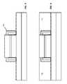
- FIG. 1shows a cross-sectional plan view of portions of an interleaved array of DRAM devices according to aspects of the invention.
- Each respective device 50 a - dis a FinFET device comprising a fin 55 , storage capacitor 60 , and bit line contact 65 .
- back-gates 70 and word lines 75are arranged laterally to the sides of the fins 55 .
- a single back gate 70is associated with and arranged to control at least two devices (e.g., 50 a and 50 c ).
- the back gate 70continues in a substantially linear fashion across two (or more) devices (e.g., 50 a and 50 c ).
- the arrayis interleaved such that the storage capacitor 60 of one device (e.g., 50 a ) is in the place of the bit line contact 65 of an adjacent device (e.g., 50 b ), and vice versa.
- FIGS. 2-20show fabrication processes and respective structures for manufacturing a structure in accordance with the present invention.
- FIG. 2shows a beginning structure for forming devices according to aspects of the invention.
- a doped region 85is formed as a doped region within a substrate (not shown).
- the doped region 85may be either an N-type region or a P-type region, depending upon the desired intended use of the semiconductor structure.
- an insulator 90Formed on a top surface of the doped region 85 is an insulator 90 , such as a buried oxide (BOX).
- BOX 90Formed on a top surface of the BOX 90 is an active silicon region 95 .
- pad films 100are Formed on a top surface of the active silicon 95 , which may comprise, for example, an SiO 2 layer formed on the active silicon 95 and an Si 3 N 4 layer formed on the SiO 2 layer. All of the layers described thus far (e.g., 85 , 90 , 95 , 100 ) may be formed using conventional semiconductor processing techniques.
- FIG. 3shows the structure of FIG. 2 after a number of intermediate processing steps, and corresponds to a cross section along line A-A of FIG. 1 .
- capacitor 60has been formed in the layers 85 , 90 , and 95 .
- a trench capacitor dielectric 105surrounds a trench conductor 110 in the capacitor 60 .
- the trench capacitor dielectric 105may be composed of, for example, an oxynitride, high-k dielectric, etc.
- the trench conductor 110may be formed of doped polysilicon.
- the trench conductor 110may be formed of a titanium nitride liner surrounding aluminum or doped polysilicon.
- the inventionis not limited to these materials, and any suitable materials may be used for the trench capacitor dielectric 105 and the trench conductor 110 .
- the intermediate process steps for forming the structure of FIG. 3may include, for example: forming a trench in the pad films 100 (e.g., using conventional patterning and etching, such as photolithography and reactive ion etching (RIE)), forming a corresponding trench in the layers 85 , 90 , and 95 (e.g., using RIE); depositing the trench capacitor dielectric 105 (e.g., using chemical vapor deposition (CVD), atomic layer deposition (ALD), etc.); form filling the trench conductor 110 ; planarizing the top surface of the structure (e.g., using chemical mechanical polish (CMP); etching the trench conductor 110 down to a level within the BOX layer 90 (e.g., below the active silicon 95 ); etching back the pad films away from the trench; removing any trench dielectric exposed by the etching of the trench conductor 110 (e.g., using wet etch, isotropic etch, etc.); growing, optionally selectively, silicon to fill in open
- FIGS. 4-13show intermediate structures shown along line B-B of FIG. 1 during manufacturing steps according to aspects of the invention.
- the processing steps shown in FIGS. 4-13occur after the capacitor 60 has been formed, as depicted in FIG. 3 .
- a second pad film 115is formed on a top surface of the active silicon 95
- a mandrel 120is formed on a top surface of the second pad film 115 .
- the second pad film 115 and mandrel 120may be any suitable materials, and may be formed using conventional deposition techniques.
- the pad filmmay comprise, for example, oxide, nitride, or a combination of the both.
- the mandrelmay be composed of, but is not limited to, silicon dioxide, or a polyimide.
- portions of the second pad film 115 and active silicon 95are etched to expose portions of the BOX 90 .
- the etchingmay be performed using conventional etching techniques, such as photolithographic masking and RIE.
- back-gate dielectric 125is formed on all exposed surfaces (e.g., of layers 90 , 95 , 115 and 120 ).
- the back-gate dielectric 125may be composed of any suitable substance, including, but not limited to, hafnium oxide, hafnium silicate, etc.
- the back-gate dielectric 125may be formed by known techniques (e.g., deposition, thermal oxidation, etc.).
- back-gate electrode material 130is conformally deposited and anisotropically etched to form sidewall gates.
- a gate cap layer 133is formed around the gate stacks of back-gate electrode material 130 .
- the back-gate electrode material 130comprises, but it not limited to, a titanium nitride and tungsten composite.
- gate cap layer 133comprises, but it not limited to, dielectric material, such as, for example nitride or oxynitride. Subsequently, exposed back-gate dielectric 125 is removed via etching.
- a side gate dielectric isolation layer 134is formed on exposed surfaces.
- the side gate dielectric isolation layer 134may comprise Si 3 N 4 and may be formed using conventional insulator deposition techniques, such as conformal desposition.
- the inventionis not limited to Si 3 N 4 , but rather, any suitable material may be used.
- an insulator 135(e.g., SiO 2 ) is formed above the sidewall gates adjacent the mandrels 120 . Surfaces may be planarized between steps.
- the mandrelis removed to expose portions of the second pad film 115 .
- the mandrelmay be removed using RIE.
- spacers 140are formed on the second pad film 115 .
- the spacers 140may be nitride, for example, formed using a conformal nitride deposition followed by a directional etch.
- portions of the pad film 115 and active silicon 95are removed to form the fins 55 . For example, a first hard mask etch may be followed by a second silicon etch that removes any exposed silicon down to the BOX layer 90 .
- a word-line gate dielectric 145is formed on exposed surfaces and a word-line gate electrode material 150 is formed on the word-line gate dielectric 145 .
- the word-line gate dielectric 145includes hafnium oxide, hafnium silicate, etc., although any suitable material may be used.
- the word-line gate electrode material 150is composed of any suitable conductor, including, but not limited to: titanium nitride, tungsten, doped polysilicon, etc.
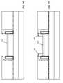
- FIG. 14shows a cross section of an intermediate structure along line A-A following the processing steps described above with respect to FIGS. 2-13 but prior to patterning and etching of the word-line.
- the processing steps described above with respect to FIGS. 4-13result in the formation of, among other things, back-gate electrode material 130 and word-line gate electrode material 150 on opposite side of fins 55 in the vicinity of the capacitor 60 and where the bit line contact will later be formed (e.g., along line A-A of FIG. 1 ).
- FIG. 15shows a cross section of an intermediate structure along line A-A after patterning and etching of the word-line.
- the word line patterning and etchingcomprises conventional masking and etching techniques performed for the selective removal of the word-line gate dielectric and word-line gate electrode material from predetermined areas of the array (e.g., in the vicinity of line A-A), such that a word line is formed on a side of each fin 55 opposite the back gate 70 (e.g., in the vicinity of line B-B), as depicted in FIG. 1 .
- the word line patterning and etchingexposes contacts 155 for the capacitor 60 and a bit line contact (such as 65 shown in FIG.
- the portions of the fins 55 that will serve as the source and drain for each respective FinFET devicemay be doped using conventional techniques, such as masking and ion-implantation of suitable ions.
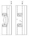
- FIGS. 16-20depict processing steps and cross sections of intermediate structures along line A-A of FIG. 1 , after word line patterning and etching as described above with respect to FIGS. 14 and 15 , according to aspects of the invention.
- the opening between the finsis filled with an insulator material 160 .
- the insulator material 160may be the same as insulator 135 (e.g., SiO 2 ), and may be formed using conventional methods.
- a patterned etchis performed to produce trenches 165 around the contacts 155 .
- the trenchesare filled with a conductor 170 , such as, for example, doped polysilicon, copper, tungsten, etc.
- a layer of insulator material 171e.g., SiO 2
- a trench 172is formed in the layer of insulator material 171 over contacts 155 not associated with a capacitor 60 .
- the trench 172is filled with a conductor 173 (such as, for example, copper, tungsten, etc.), thereby forming a bit line contact 65 (such as that shown in FIG. 1 ).
- BEOLback end of line
- the manufacturing steps described with respect to FIGS. 2-20may be used to create an array of dynamic random access memory cells, such as that shown in FIG. 1 .
- the semiconductor structures shown in FIGS. 2-20are cross sections along lines A-A and B-B (e.g., devices 50 a and 50 b in FIG. 1 )
- similar processing stepsmay be concurrently performed to create any desired number of devices in an array (e.g., 50 c and 50 d in FIG. 1 ).
- a single back-gate formed using the processing steps of FIGS. 2-20may be formed in association with a plurality of devices in an array.
- an array having two back gates and four deviceshas been described thusfar, the invention is not limited to this number of devices, and any suitable number of devices can be used in an array in accordance with aspects of the invention.
- FIGS. 21-27show fabrication processes and intermediate structures for forming an interleaved array of DRAM memory devices in accordance with the invention, such as, for example, that shown in FIG. 1 .
- the capacitoris formed over the fin, instead of under the fin (as in FIGS. 3-20 ).
- the structure shown in FIG. 21may be arrived at using the same processing steps as described above with respect to FIGS. 2-18 , excluding the formation of the capacitors described with respect to FIG. 3 .
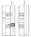
- FIG. 21shows a number of contacts 155 formed on a top surface of the BOX layer 90 , for example, at the line A-A of FIG. 1 .
- Each contact 155comprises a portion of a fin 55 associated with a respective back-gate 70 , and in electrical contact with conductor 170 .
- a second layer of dielectric material 175is deposited on exposed surfaces (e.g., the insulator materials, and the conductor).
- the second layer of dielectric material 175may comprise any suitable material, such as, for example, SiO 2 .
- Trenches 180which will hold the storage capacitors (not yet formed), are created in the second layer of dielectric material 175 , using, for example, conventional patterning and etching techniques.
- a conductive liner 185is conformally deposited on the exposed surfaces of the second layer of dielectric material 175 , including inside the trenches 180 .
- the conductive liner 185may be composed of, but is not limited to, titanium nitride, tantalum nitride, etc.
- a storage dielectric material 190is deposited on the conductive liner 185 .
- the storage dielectric material 190is composed of high-k dielectric, such as hafnium silicate, although other suitable materials may be used.
- a trench conductor 195is deposited on exposed surfaces.
- the trench conductor 195may comprise, but is not limited to, a liner of titanium nitride or tantalum nitride with tungsten or doped polysilicon fill.
- the structureis planarized, e.g., using a CMP process, thereby removing portions of the conductive liner 185 , the storage dielectric material 190 , and the trench conductor 195 .
- FIG. 26shows a third dielectric layer 200 formed on a top surface of the second dielectric layer 175 .
- Trenches 205are formed through the third dielectric layer 200 , down to the trench conductor 195 .
- Trenches 210are formed through the third dielectric layer 200 and the second dielectric layer 175 , down to the conductor 170 .
- the trenches 205 and 210are filled with any suitable conductor 215 , thereby forming interleaved capacitors 60 and bit line contacts 65 (e.g., as shown in FIG. 1 ).
- BEOLback end of line
- conventional interconnect processesmay be used to providing wiring that completes the array.
- FIG. 27shows an alternative configuration of an interleaved array of DRAM devices according to aspects of the invention.
- the arrayincludes fins 55 , word lines 75 , back-gates 70 , bit line contacts 65 , and storage capacitors 60 , either formed downward from the fin 55 (e.g., as shown in FIG. 20 ) or formed upward from the fin 55 (e.g., as shown in FIG. 26 ).
- Back-gate contacts 220 , word-line contacts 225 , and wires 230 connected to the bit line contacts 65may also be employed.
- FIG. 28shows a block diagram of an exemplary design flow 900 used for example, in semiconductor IC logic design, simulation, test, layout, and manufacture.
- Design flow 900includes processes and mechanisms for processing design structures or devices to generate logically or otherwise functionally equivalent representations of the design structures and/or devices described above and shown in FIGS. 1-27 .
- the design structures processed and/or generated by design flow 900may be encoded on machine-readable transmission or storage media to include data and/or instructions that when executed or otherwise processed on a data processing system generate a logically, structurally, mechanically, or otherwise functionally equivalent representation of hardware components, circuits, devices, or systems.
- Design flow 900may vary depending on the type of representation being designed.
- a design flow 900 for building an application specific ICmay differ from a design flow 900 for designing a standard component or from a design flow 900 for instantiating the design into a programmable array, for example a programmable gate array (PGA) or a field programmable gate array (FPGA) offered by Altera® Inc. or Xilinx® Inc.
- PGAprogrammable gate array
- FPGAfield programmable gate array
- FIG. 28illustrates multiple such design structures including an input design structure 920 that is preferably processed by a design process 910 .
- Design structure 920may be a logical simulation design structure generated and processed by design process 910 to produce a logically equivalent functional representation of a hardware device.
- Design structure 920may also or alternatively comprise data and/or program instructions that when processed by design process 910 , generate a functional representation of the physical structure of a hardware device. Whether representing functional and/or structural design features, design structure 920 may be generated using electronic computer-aided design (ECAD) such as implemented by a core developer/designer.
- ECADelectronic computer-aided design
- design structure 920When encoded on a machine-readable data transmission, gate array, or storage medium, design structure 920 may be accessed and processed by one or more hardware and/or software modules within design process 910 to simulate or otherwise functionally represent an electronic component, circuit, electronic or logic module, apparatus, device, or system such as those shown in FIGS. 1-27 .
- design structure 920may comprise files or other data structures including human and/or machine-readable source code, compiled structures, and computer-executable code structures that when processed by a design or simulation data processing system, functionally simulate or otherwise represent circuits or other levels of hardware logic design.
- Such data structuresmay include hardware-description language (HDL) design entities or other data structures conforming to and/or compatible with lower-level HDL design languages such as Verilog and VHDL, and/or higher level design languages such as C or C++.
- HDLhardware-description language
- Design process 910preferably employs and incorporates hardware and/or software modules for synthesizing, translating, or otherwise processing a design/simulation functional equivalent of the components, circuits, devices, or logic structures shown in FIGS. 1-27 to generate a netlist 980 which may contain design structures such as design structure 920 .
- Netlist 980may comprise, for example, compiled or otherwise processed data structures representing a list of wires, discrete components, logic gates, control circuits, I/O devices, models, etc. that describes the connections to other elements and circuits in an integrated circuit design.
- Netlist 980may be synthesized using an iterative process in which netlist 980 is resynthesized one or more times depending on design specifications and parameters for the device.
- netlist 980may be recorded on a machine-readable data storage medium or programmed into a programmable gate array.
- the mediummay be a non-volatile storage medium such as a magnetic or optical disk drive, a programmable gate array, a compact flash, or other flash memory. Additionally, or in the alternative, the medium may be a system or cache memory, buffer space, or electrically or optically conductive devices and materials on which data packets may be transmitted and intermediately stored via the Internet, or other networking suitable means.
- Design process 910may include hardware and software modules for processing a variety of input data structure types including netlist 980 .
- data structure typesmay reside, for example, within library elements 930 and include a set of commonly used elements, circuits, and devices, including models, layouts, and symbolic representations, for a given manufacturing technology (e.g., different technology nodes, 32 nm, 45 nm, 90 nm, etc.).
- the data structure typesmay further include design specifications 940 , characterization data 950 , verification data 960 , design rules 970 , and test data files 985 which may include input test patterns, output test results, and other testing information.
- Design process 910may further include, for example, standard mechanical design processes such as stress analysis, thermal analysis, mechanical event simulation, process simulation for operations such as casting, molding, and die press forming, etc.
- standard mechanical design processessuch as stress analysis, thermal analysis, mechanical event simulation, process simulation for operations such as casting, molding, and die press forming, etc.
- One of ordinary skill in the art of mechanical designcan appreciate the extent of possible mechanical design tools and applications used in design process 910 without deviating from the scope and spirit of the invention.
- Design process 910may also include modules for performing standard circuit design processes such as timing analysis, verification, design rule checking, place and route operations, etc.
- Design process 910employs and incorporates logic and physical design tools such as HDL compilers and simulation model build tools to process design structure 920 together with some or all of the depicted supporting data structures along with any additional mechanical design or data (if applicable), to generate a second design structure 990 .
- Design structure 990resides on a storage medium or programmable gate array in a data format used for the exchange of data of mechanical devices and structures (e.g. information stored in a IGES, DXF, Parasolid XT, JT, DRG, or any other suitable format for storing or rendering such mechanical design structures).
- design structure 990preferably comprises one or more files, data structures, or other computer-encoded data or instructions that reside on transmission or data storage media and that when processed by an ECAD system generate a logically or otherwise functionally equivalent form of one or more of the embodiments of the invention shown in FIGS. 1-27 .
- design structure 990may comprise a compiled, executable HDL simulation model that functionally simulates the devices shown in FIGS. 1-27 .
- Design structure 990may also employ a data format used for the exchange of layout data of integrated circuits and/or symbolic data format (e.g. information stored in a GDSII (GDS2), GL1, OASIS, map files, or any other suitable format for storing such design data structures).
- Design structure 990may comprise information such as, for example, symbolic data, map files, test data files, design content files, manufacturing data, layout parameters, wires, levels of metal, vias, shapes, data for routing through the manufacturing line, and any other data required by a manufacturer or other designer/developer to produce a device or structure as described above and shown in FIGS. 1-27 .
- Design structure 990may then proceed to a stage 995 where, for example, design structure 990 : proceeds to tape-out, is released to manufacturing, is released to a mask house, is sent to another design house, is sent back to the customer, etc.
- the method as described aboveis used in the fabrication of integrated circuit chips.
- the resulting integrated circuit chipscan be distributed by the fabricator in raw wafer form (that is, as a single wafer that has multiple unpackaged chips), as a bare die, or in a packaged form.
- the chipis mounted in a single chip package (such as a plastic carrier, with leads that are affixed to a motherboard or other higher level carrier) or in a multichip package (such as a ceramic carrier that has either or both surface interconnections or buried interconnections).
- the chipis then integrated with other chips, discrete circuit elements, and/or other signal processing devices as part of either (a) an intermediate product, such as a motherboard, or (b) an end product.
- the end productcan be any product that includes integrated circuit chips.
Landscapes
- Engineering & Computer Science (AREA)
- Manufacturing & Machinery (AREA)
- Semiconductor Memories (AREA)
Abstract
Description
- Applicant claims the benefit of Provisional Application Ser. No. 61/159,815, Split-Gate Dram With Lateral Control-Gate Mugfet filed on Mar. 13, 2009.
- The invention relates to semiconductor devices used for memory applications, and more particularly, to a design structure, structure, and method for providing a split-gate DRAM with MuGFET.
- DRAM (Dynamic Random Access Memory) is desirable over SRAM (Static Random Access Memory) in many situations because DRAM arrays can be denser and DRAM devices require less power to operate. As semiconductor device sizes continue to decrease (for example, toward the 22 nanometer node, and smaller), single gate devices begin to experience performance degradation, such as short channel effects. Accordingly, there is a trend toward using multiple gate field effect transistor devices (e.g., MuGFET). Some conventional DRAM devices employ a planar transistor with a gate beneath the channel and a word line above the channel. However, these arrangements exhibit relatively low performance and can only be arranged in low-density arrays.
- A challenge facing DRAM improvement is the reduction of operating power even lower than what it is currently employed. This is at least partly due to the phenomenon of leakage. For example, when threshold voltage of a fin-type field effect transistor (FinFET) DRAM device is reduced too far, leakage becomes a significant concern. The threshold voltage of FinFET retards leakage of stored charge out of the capacitance structure of the DRAM. Leakage increases as threshold voltage decreases, thereby requiring more frequent updating of the capacitance structure of the DRAM.
- However, it is desirable in some circumstances to have a low threshold voltage, because a lower threshold voltage permits a lower wordline voltage to be utilized with the DRAM device. Put another way, when the threshold voltage is kept high to prevent undesirable leakage, the wordline voltage during write and read operations must also be high to overcome the threshold voltage. Since the wordline voltage is directly related to the operating power required to drive a DRAM device, leakage is generally in conflict with lowering the operating power.
- Accordingly, there exists a need in the art to overcome the deficiencies and limitations described hereinabove.
- In a first aspect of the invention, there is a semiconductor structure of an array of dynamic random access memory cells. The structure comprises: a first fin of a first split-gate fin-type field effect transistor (FinFET) device on a substrate; a second fin of a second split-gate fin-type field effect transistor (FinFET) device on the substrate; and a back-gate associated with the first fin and the second fin. The back-gate influences a threshold voltage of the first fin and a threshold voltage of the second fin. One embodiment of the invention combines the first fin with a first storage capacitor, and combines the second fin with a second storage capacitor.
- In a second aspect of the invention, there is a design structure tangibly embodied in a machine readable medium for designing, manufacturing, or testing an integrated circuit. The design structure comprises a semiconductor structure as described above.
- In a third aspect of the invention, there is a method of controlling an array of dynamic random access memory cells, comprising: arranging a back-gate in association with a first plurality of split-gate fin-type field effect transistor (FinFET) devices in the array; and selectively influencing a voltage in a fin of each of the plurality of FinFET devices between a first threshold voltage and a second threshold voltage using the back-gate.
- The present invention is described in the detailed description which follows, in reference to the noted plurality of drawings by way of non-limiting examples of exemplary embodiments of the present invention.
FIG. 1 shows a cross-sectional plan view of portions of an interleaved array of DRAM devices according to aspects of the invention;FIGS. 2-20 show fabrication processes and respective structures for manufacturing a structure in accordance with aspects of the invention;FIGS. 21-26 show fabrication processes and respective structures for manufacturing a structure in accordance with aspects of the invention;FIG. 27 shows a cross-sectional plan view of portions of another arrangement of an interleaved array of DRAM devices according to aspects of the invention; andFIG. 28 is a flow diagram of a design process used in semiconductor design, manufacture, and/or test.- The invention relates to semiconductor devices used for memory applications, and more particularly, to a design structure, structure, and method for providing a split-gate DRAM with MuGFET. In embodiments of the invention, a DRAM device comprises a FinFET having a wordline on a first lateral side of a vertical fin and a back-gate on an opposite lateral side of the fin. According to aspects of the invention, a single back gate is associated with plural memory cells. For example, a single back gate may be arranged adjacent to plural fins of at least two neighboring memory cells. In this manner, the threshold voltage of the fin of each of the memory cells may be controlled by controlling the electrical potential of the single back gate.
- In embodiments of the invention, the DRAM device operates in at least two modes. In a first mode (e.g., standby mode), the back-gate is biased relatively negative (e.g., to about ˜1.0 v), which results in a high threshold voltage in all fins associated with the back-gate, which reduces subthreshold channel leakage. In a second mode of operation (e.g., read/write mode, also referred to as access mode), the back-gate is biased to a relatively positive level (e.g., about 0 to +1.0 v), which lowers the threshold voltage in all of the fins associated with the back-gate, which reduces the amount of voltage required on the wordline to read from or write to the storage structure (e.g., capacitor) of the DRAM, and hence reduces the required power for a read or a write operation. In this manner, plural devices can be placed in standby mode or access mode at the same time using a single back gate. When the plural devices are placed in access mode, respective ones of the devices may be accessed by applying an appropriate voltage to the respective word-lines.
- In this manner, embodiments of the invention include a DRAM device that operates at relatively low power while reducing the effect of leakage. Moreover, by using a vertical fin and split gates with a single back-gate arranged to control multiple devices, implementations of the invention provide this low-power DRAM device in dense arrays.
FIG. 1 shows a cross-sectional plan view of portions of an interleaved array of DRAM devices according to aspects of the invention. Each respective device50a-dis a FinFET device comprising afin 55,storage capacitor 60, andbit line contact 65. In embodiments, back-gates 70 andword lines 75 are arranged laterally to the sides of thefins 55. In embodiments asingle back gate 70 is associated with and arranged to control at least two devices (e.g.,50aand50c). According to aspects of the invention, theback gate 70 continues in a substantially linear fashion across two (or more) devices (e.g.,50aand50c). In embodiments, the array is interleaved such that thestorage capacitor 60 of one device (e.g.,50a) is in the place of thebit line contact 65 of an adjacent device (e.g.,50b), and vice versa.FIGS. 2-20 show fabrication processes and respective structures for manufacturing a structure in accordance with the present invention.FIG. 2 shows a beginning structure for forming devices according to aspects of the invention. As depicted inFIG. 2 , adoped region 85 is formed as a doped region within a substrate (not shown). Thedoped region 85 may be either an N-type region or a P-type region, depending upon the desired intended use of the semiconductor structure. Formed on a top surface of thedoped region 85 is aninsulator 90, such as a buried oxide (BOX). Formed on a top surface of theBOX 90 is anactive silicon region 95. Formed on a top surface of theactive silicon 95 arepad films 100, which may comprise, for example, an SiO2layer formed on theactive silicon 95 and an Si3N4layer formed on the SiO2layer. All of the layers described thus far (e.g.,85,90,95,100) may be formed using conventional semiconductor processing techniques.FIG. 3 shows the structure ofFIG. 2 after a number of intermediate processing steps, and corresponds to a cross section along line A-A ofFIG. 1 . As depicted inFIG. 3 ,capacitor 60 has been formed in thelayers capacitor 60. The trench capacitor dielectric105 may be composed of, for example, an oxynitride, high-k dielectric, etc. In embodiments, when thetrench capacitor dielectric 105 is an oxynitride, thetrench conductor 110 may be formed of doped polysilicon. Alternatively, when thetrench capacitor dielectric 105 is a high-k dielectric, thetrench conductor 110 may be formed of a titanium nitride liner surrounding aluminum or doped polysilicon. However, the invention is not limited to these materials, and any suitable materials may be used for thetrench capacitor dielectric 105 and thetrench conductor 110.- The intermediate process steps for forming the structure of
FIG. 3 may include, for example: forming a trench in the pad films100 (e.g., using conventional patterning and etching, such as photolithography and reactive ion etching (RIE)), forming a corresponding trench in thelayers trench conductor 110; planarizing the top surface of the structure (e.g., using chemical mechanical polish (CMP); etching thetrench conductor 110 down to a level within the BOX layer90 (e.g., below the active silicon95); etching back the pad films away from the trench; removing any trench dielectric exposed by the etching of the trench conductor110 (e.g., using wet etch, isotropic etch, etc.); growing, optionally selectively, silicon to fill in open portions of the trench between thetrench conductor 110 and theactive silicon 95; and stripping the remaining pad films100 (e.g., using selective RIE, then a wet or dry etch). FIGS. 4-13 show intermediate structures shown along line B-B ofFIG. 1 during manufacturing steps according to aspects of the invention. In embodiments, the processing steps shown inFIGS. 4-13 occur after thecapacitor 60 has been formed, as depicted inFIG. 3 . As depicted inFIG. 4 , asecond pad film 115 is formed on a top surface of theactive silicon 95, and amandrel 120 is formed on a top surface of thesecond pad film 115. Thesecond pad film 115 andmandrel 120 may be any suitable materials, and may be formed using conventional deposition techniques. The pad film may comprise, for example, oxide, nitride, or a combination of the both. The mandrel may be composed of, but is not limited to, silicon dioxide, or a polyimide.- As depicted in
FIG. 5 , portions of thesecond pad film 115 andactive silicon 95 are etched to expose portions of theBOX 90. The etching may be performed using conventional etching techniques, such as photolithographic masking and RIE. As depicted inFIG. 6 ,back-gate dielectric 125 is formed on all exposed surfaces (e.g., oflayers back-gate dielectric 125 may be composed of any suitable substance, including, but not limited to, hafnium oxide, hafnium silicate, etc. Theback-gate dielectric 125 may be formed by known techniques (e.g., deposition, thermal oxidation, etc.). - As depicted in
FIG. 7 ,back-gate electrode material 130 is conformally deposited and anisotropically etched to form sidewall gates. Also, agate cap layer 133 is formed around the gate stacks ofback-gate electrode material 130. In embodiments, theback-gate electrode material 130 comprises, but it not limited to, a titanium nitride and tungsten composite. In embodiments,gate cap layer 133 comprises, but it not limited to, dielectric material, such as, for example nitride or oxynitride. Subsequently, exposedback-gate dielectric 125 is removed via etching. - As depicted in
FIG. 8 , a side gatedielectric isolation layer 134 is formed on exposed surfaces. In embodiments, the side gatedielectric isolation layer 134 may comprise Si3N4and may be formed using conventional insulator deposition techniques, such as conformal desposition. However, the invention is not limited to Si3N4, but rather, any suitable material may be used. - As depicted in
FIG. 9 , an insulator135 (e.g., SiO2) is formed above the sidewall gates adjacent themandrels 120. Surfaces may be planarized between steps. AtFIG. 10 , the mandrel is removed to expose portions of thesecond pad film 115. The mandrel may be removed using RIE. AtFIG. 11 ,spacers 140 are formed on thesecond pad film 115. Thespacers 140 may be nitride, for example, formed using a conformal nitride deposition followed by a directional etch. AtFIG. 12 , portions of thepad film 115 andactive silicon 95 are removed to form thefins 55. For example, a first hard mask etch may be followed by a second silicon etch that removes any exposed silicon down to theBOX layer 90. - As depicted in
FIG. 13 , a word-line gate dielectric 145 is formed on exposed surfaces and a word-linegate electrode material 150 is formed on the word-line gate dielectric 145. In embodiments, the word-line gate dielectric 145 includes hafnium oxide, hafnium silicate, etc., although any suitable material may be used. In embodiments, the word-linegate electrode material 150 is composed of any suitable conductor, including, but not limited to: titanium nitride, tungsten, doped polysilicon, etc. FIG. 14 shows a cross section of an intermediate structure along line A-A following the processing steps described above with respect toFIGS. 2-13 but prior to patterning and etching of the word-line. For example, the processing steps described above with respect toFIGS. 4-13 result in the formation of, among other things,back-gate electrode material 130 and word-linegate electrode material 150 on opposite side offins 55 in the vicinity of thecapacitor 60 and where the bit line contact will later be formed (e.g., along line A-A ofFIG. 1 ).FIG. 15 shows a cross section of an intermediate structure along line A-A after patterning and etching of the word-line. In embodiments, the word line patterning and etching comprises conventional masking and etching techniques performed for the selective removal of the word-line gate dielectric and word-line gate electrode material from predetermined areas of the array (e.g., in the vicinity of line A-A), such that a word line is formed on a side of eachfin 55 opposite the back gate70 (e.g., in the vicinity of line B-B), as depicted inFIG. 1 . Moreover, as depicted inFIG. 15 , the word line patterning and etching exposescontacts 155 for thecapacitor 60 and a bit line contact (such as65 shown inFIG. 1 , not yet formed inFIG. 15 ). After the word-line patterning and etching, the portions of thefins 55 that will serve as the source and drain for each respective FinFET device may be doped using conventional techniques, such as masking and ion-implantation of suitable ions.FIGS. 16-20 depict processing steps and cross sections of intermediate structures along line A-A ofFIG. 1 , after word line patterning and etching as described above with respect toFIGS. 14 and 15 , according to aspects of the invention. AtFIG. 16 , the opening between the fins is filled with aninsulator material 160. In embodiments, theinsulator material 160 may be the same as insulator135 (e.g., SiO2), and may be formed using conventional methods. Then, as depicted atFIG. 17 , a patterned etch is performed to producetrenches 165 around thecontacts 155.- At
FIG. 18 , the trenches are filled with aconductor 170, such as, for example, doped polysilicon, copper, tungsten, etc. As depicted atFIG. 19 , a layer of insulator material171 (e.g., SiO2) is formed over exposed surfaces. Then, as shown inFIG. 20 , atrench 172 is formed in the layer ofinsulator material 171 overcontacts 155 not associated with acapacitor 60. Still referring toFIG. 20 , thetrench 172 is filled with a conductor173 (such as, for example, copper, tungsten, etc.), thereby forming a bit line contact65 (such as that shown inFIG. 1 ). At this point, conventional back end of line (BEOL) processing techniques may be used to finish the array. For example, conventional interconnect processes may be used to providing wiring that completes the array. - In embodiments, the manufacturing steps described with respect to
FIGS. 2-20 may be used to create an array of dynamic random access memory cells, such as that shown inFIG. 1 . For example, although the semiconductor structures shown inFIGS. 2-20 are cross sections along lines A-A and B-B (e.g.,devices FIG. 1 ), it is understood that in embodiments of the invention similar processing steps may be concurrently performed to create any desired number of devices in an array (e.g.,50cand50dinFIG. 1 ). In this manner, a single back-gate formed using the processing steps ofFIGS. 2-20 may be formed in association with a plurality of devices in an array. Moreover, although an array having two back gates and four devices has been described thusfar, the invention is not limited to this number of devices, and any suitable number of devices can be used in an array in accordance with aspects of the invention. FIGS. 21-27 show fabrication processes and intermediate structures for forming an interleaved array of DRAM memory devices in accordance with the invention, such as, for example, that shown inFIG. 1 . However, in the devices shown inFIGS. 21-27 , the capacitor is formed over the fin, instead of under the fin (as inFIGS. 3-20 ). The structure shown inFIG. 21 may be arrived at using the same processing steps as described above with respect toFIGS. 2-18 , excluding the formation of the capacitors described with respect toFIG. 3 . Accordingly,FIG. 21 shows a number ofcontacts 155 formed on a top surface of theBOX layer 90, for example, at the line A-A ofFIG. 1 . Eachcontact 155 comprises a portion of afin 55 associated with arespective back-gate 70, and in electrical contact withconductor 170.- As depicted in
FIG. 22 , a second layer ofdielectric material 175 is deposited on exposed surfaces (e.g., the insulator materials, and the conductor). The second layer ofdielectric material 175 may comprise any suitable material, such as, for example, SiO2.Trenches 180, which will hold the storage capacitors (not yet formed), are created in the second layer ofdielectric material 175, using, for example, conventional patterning and etching techniques. - As depicted in
FIG. 23 , aconductive liner 185 is conformally deposited on the exposed surfaces of the second layer ofdielectric material 175, including inside thetrenches 180. Theconductive liner 185 may be composed of, but is not limited to, titanium nitride, tantalum nitride, etc. Subsequently, astorage dielectric material 190 is deposited on theconductive liner 185. In embodiments, thestorage dielectric material 190 is composed of high-k dielectric, such as hafnium silicate, although other suitable materials may be used. - As depicted in
FIG. 24 , atrench conductor 195 is deposited on exposed surfaces. Thetrench conductor 195 may comprise, but is not limited to, a liner of titanium nitride or tantalum nitride with tungsten or doped polysilicon fill. Then, as shown inFIG. 25 , the structure is planarized, e.g., using a CMP process, thereby removing portions of theconductive liner 185, thestorage dielectric material 190, and thetrench conductor 195. FIG. 26 shows a thirddielectric layer 200 formed on a top surface of thesecond dielectric layer 175.Trenches 205 are formed through the thirddielectric layer 200, down to thetrench conductor 195.Trenches 210 are formed through the thirddielectric layer 200 and thesecond dielectric layer 175, down to theconductor 170. Thetrenches suitable conductor 215, thereby forming interleavedcapacitors 60 and bit line contacts65 (e.g., as shown inFIG. 1 ). At this point, conventional back end of line (BEOL) processing techniques may be used to finish the array. For example, conventional interconnect processes may be used to providing wiring that completes the array. Although an array having four devices has been described thusfar, the invention is not limited to this number of devices, and any suitable number of devices can be used in an array in accordance with aspects of the invention.FIG. 27 shows an alternative configuration of an interleaved array of DRAM devices according to aspects of the invention. The array includesfins 55, word lines75, back-gates 70,bit line contacts 65, andstorage capacitors 60, either formed downward from the fin55 (e.g., as shown inFIG. 20 ) or formed upward from the fin55 (e.g., as shown inFIG. 26 ).Back-gate contacts 220, word-line contacts 225, andwires 230 connected to thebit line contacts 65 may also be employed.FIG. 28 shows a block diagram of anexemplary design flow 900 used for example, in semiconductor IC logic design, simulation, test, layout, and manufacture.Design flow 900 includes processes and mechanisms for processing design structures or devices to generate logically or otherwise functionally equivalent representations of the design structures and/or devices described above and shown inFIGS. 1-27 . The design structures processed and/or generated bydesign flow 900 may be encoded on machine-readable transmission or storage media to include data and/or instructions that when executed or otherwise processed on a data processing system generate a logically, structurally, mechanically, or otherwise functionally equivalent representation of hardware components, circuits, devices, or systems.Design flow 900 may vary depending on the type of representation being designed. For example, adesign flow 900 for building an application specific IC (ASIC) may differ from adesign flow 900 for designing a standard component or from adesign flow 900 for instantiating the design into a programmable array, for example a programmable gate array (PGA) or a field programmable gate array (FPGA) offered by Altera® Inc. or Xilinx® Inc.FIG. 28 illustrates multiple such design structures including aninput design structure 920 that is preferably processed by adesign process 910.Design structure 920 may be a logical simulation design structure generated and processed bydesign process 910 to produce a logically equivalent functional representation of a hardware device.Design structure 920 may also or alternatively comprise data and/or program instructions that when processed bydesign process 910, generate a functional representation of the physical structure of a hardware device. Whether representing functional and/or structural design features,design structure 920 may be generated using electronic computer-aided design (ECAD) such as implemented by a core developer/designer. When encoded on a machine-readable data transmission, gate array, or storage medium,design structure 920 may be accessed and processed by one or more hardware and/or software modules withindesign process 910 to simulate or otherwise functionally represent an electronic component, circuit, electronic or logic module, apparatus, device, or system such as those shown inFIGS. 1-27 . As such,design structure 920 may comprise files or other data structures including human and/or machine-readable source code, compiled structures, and computer-executable code structures that when processed by a design or simulation data processing system, functionally simulate or otherwise represent circuits or other levels of hardware logic design. Such data structures may include hardware-description language (HDL) design entities or other data structures conforming to and/or compatible with lower-level HDL design languages such as Verilog and VHDL, and/or higher level design languages such as C or C++.Design process 910 preferably employs and incorporates hardware and/or software modules for synthesizing, translating, or otherwise processing a design/simulation functional equivalent of the components, circuits, devices, or logic structures shown inFIGS. 1-27 to generate anetlist 980 which may contain design structures such asdesign structure 920.Netlist 980 may comprise, for example, compiled or otherwise processed data structures representing a list of wires, discrete components, logic gates, control circuits, I/O devices, models, etc. that describes the connections to other elements and circuits in an integrated circuit design.Netlist 980 may be synthesized using an iterative process in which netlist980 is resynthesized one or more times depending on design specifications and parameters for the device. As with other design structure types described herein,netlist 980 may be recorded on a machine-readable data storage medium or programmed into a programmable gate array. The medium may be a non-volatile storage medium such as a magnetic or optical disk drive, a programmable gate array, a compact flash, or other flash memory. Additionally, or in the alternative, the medium may be a system or cache memory, buffer space, or electrically or optically conductive devices and materials on which data packets may be transmitted and intermediately stored via the Internet, or other networking suitable means.Design process 910 may include hardware and software modules for processing a variety of input data structuretypes including netlist 980. Such data structure types may reside, for example, withinlibrary elements 930 and include a set of commonly used elements, circuits, and devices, including models, layouts, and symbolic representations, for a given manufacturing technology (e.g., different technology nodes, 32 nm, 45 nm, 90 nm, etc.). The data structure types may further includedesign specifications 940,characterization data 950,verification data 960,design rules 970, and test data files985 which may include input test patterns, output test results, and other testing information.Design process 910 may further include, for example, standard mechanical design processes such as stress analysis, thermal analysis, mechanical event simulation, process simulation for operations such as casting, molding, and die press forming, etc. One of ordinary skill in the art of mechanical design can appreciate the extent of possible mechanical design tools and applications used indesign process 910 without deviating from the scope and spirit of the invention.Design process 910 may also include modules for performing standard circuit design processes such as timing analysis, verification, design rule checking, place and route operations, etc.Design process 910 employs and incorporates logic and physical design tools such as HDL compilers and simulation model build tools to processdesign structure 920 together with some or all of the depicted supporting data structures along with any additional mechanical design or data (if applicable), to generate asecond design structure 990.Design structure 990 resides on a storage medium or programmable gate array in a data format used for the exchange of data of mechanical devices and structures (e.g. information stored in a IGES, DXF, Parasolid XT, JT, DRG, or any other suitable format for storing or rendering such mechanical design structures). Similar to designstructure 920,design structure 990 preferably comprises one or more files, data structures, or other computer-encoded data or instructions that reside on transmission or data storage media and that when processed by an ECAD system generate a logically or otherwise functionally equivalent form of one or more of the embodiments of the invention shown inFIGS. 1-27 . In one embodiment,design structure 990 may comprise a compiled, executable HDL simulation model that functionally simulates the devices shown inFIGS. 1-27 .Design structure 990 may also employ a data format used for the exchange of layout data of integrated circuits and/or symbolic data format (e.g. information stored in a GDSII (GDS2), GL1, OASIS, map files, or any other suitable format for storing such design data structures).Design structure 990 may comprise information such as, for example, symbolic data, map files, test data files, design content files, manufacturing data, layout parameters, wires, levels of metal, vias, shapes, data for routing through the manufacturing line, and any other data required by a manufacturer or other designer/developer to produce a device or structure as described above and shown inFIGS. 1-27 .Design structure 990 may then proceed to astage 995 where, for example, design structure990: proceeds to tape-out, is released to manufacturing, is released to a mask house, is sent to another design house, is sent back to the customer, etc.- The method as described above is used in the fabrication of integrated circuit chips. The resulting integrated circuit chips can be distributed by the fabricator in raw wafer form (that is, as a single wafer that has multiple unpackaged chips), as a bare die, or in a packaged form. In the latter case the chip is mounted in a single chip package (such as a plastic carrier, with leads that are affixed to a motherboard or other higher level carrier) or in a multichip package (such as a ceramic carrier that has either or both surface interconnections or buried interconnections). In any case the chip is then integrated with other chips, discrete circuit elements, and/or other signal processing devices as part of either (a) an intermediate product, such as a motherboard, or (b) an end product. The end product can be any product that includes integrated circuit chips.
- The terminology used herein is for the purpose of describing particular embodiments only and is not intended to be limiting of the invention. As used herein, the singular forms “a”, “an” and “the” are intended to include the plural forms as well, unless the context clearly indicates otherwise. It will be further understood that the terms “comprises” and/or “comprising,” when used in this specification, specify the presence of stated features, integers, steps, operations, elements, and/or components, but do not preclude the presence or addition of one or more other features, integers, steps, operations, elements, components, and/or groups thereof.
- The corresponding structures, materials, acts, and equivalents of all means or step plus function elements, if any, in the claims below are intended to include any structure, material, or act for performing the function in combination with other claimed elements as specifically claimed. The description of the present invention has been presented for purposes of illustration and description, but is not intended to be exhaustive or limited to the invention in the form disclosed. Many modifications and variations will be apparent to those of ordinary skill in the art without departing from the scope and spirit of the invention. The embodiments were chosen and described in order to best explain the principles of the invention and the practical application, and to enable others of ordinary skill in the art to understand the invention for various embodiments with various modifications as are suited to the particular use contemplated.
Claims (20)
Priority Applications (1)
| Application Number | Priority Date | Filing Date | Title |
|---|---|---|---|
| US12/538,196US8184472B2 (en) | 2009-03-13 | 2009-08-10 | Split-gate DRAM with lateral control-gate MuGFET |
Applications Claiming Priority (2)
| Application Number | Priority Date | Filing Date | Title |
|---|---|---|---|
| US15981509P | 2009-03-13 | 2009-03-13 | |
| US12/538,196US8184472B2 (en) | 2009-03-13 | 2009-08-10 | Split-gate DRAM with lateral control-gate MuGFET |
Publications (2)
| Publication Number | Publication Date |
|---|---|
| US20100232212A1true US20100232212A1 (en) | 2010-09-16 |
| US8184472B2 US8184472B2 (en) | 2012-05-22 |
Family
ID=42730586
Family Applications (1)
| Application Number | Title | Priority Date | Filing Date |
|---|---|---|---|
| US12/538,196Active2030-02-18US8184472B2 (en) | 2009-03-13 | 2009-08-10 | Split-gate DRAM with lateral control-gate MuGFET |
Country Status (1)
| Country | Link |
|---|---|
| US (1) | US8184472B2 (en) |
Cited By (31)
| Publication number | Priority date | Publication date | Assignee | Title |
|---|---|---|---|---|
| US20100038694A1 (en)* | 2008-08-15 | 2010-02-18 | Anderson Brent A | Split-gate dram with mugfet, design structure, and method of manufacture |
| US20100187622A1 (en)* | 2008-03-13 | 2010-07-29 | Tela Innovations, Inc. | Linear Gate Level Cross-Coupled Transistor Device with Complimentary Pairs of Cross-Coupled Transistors Defined by Physically Separate Gate Electrodes within Gate Electrode Level |
| US20100287518A1 (en)* | 2009-05-06 | 2010-11-11 | Tela Innovations, Inc. | Cell Circuit and Layout with Linear Finfet Structures |
| US8129755B2 (en) | 2006-03-09 | 2012-03-06 | Tela Innovations, Inc. | Integrated circuit with gate electrode level including at least four linear-shaped conductive structures of equal length and equal pitch with linear-shaped conductive structure forming one transistor |
| US8214778B2 (en) | 2007-08-02 | 2012-07-03 | Tela Innovations, Inc. | Methods for cell phasing and placement in dynamic array architecture and implementation of the same |
| US8225239B2 (en) | 2006-03-09 | 2012-07-17 | Tela Innovations, Inc. | Methods for defining and utilizing sub-resolution features in linear topology |
| US8225261B2 (en) | 2006-03-09 | 2012-07-17 | Tela Innovations, Inc. | Methods for defining contact grid in dynamic array architecture |
| US8245180B2 (en) | 2006-03-09 | 2012-08-14 | Tela Innovations, Inc. | Methods for defining and using co-optimized nanopatterns for integrated circuit design and apparatus implementing same |
| US8247846B2 (en) | 2006-03-09 | 2012-08-21 | Tela Innovations, Inc. | Oversized contacts and vias in semiconductor chip defined by linearly constrained topology |
| US8286107B2 (en) | 2007-02-20 | 2012-10-09 | Tela Innovations, Inc. | Methods and systems for process compensation technique acceleration |
| US8283701B2 (en) | 2007-08-02 | 2012-10-09 | Tela Innovations, Inc. | Semiconductor device with dynamic array sections defined and placed according to manufacturing assurance halos |
| CN102983131A (en)* | 2011-10-07 | 2013-03-20 | 钰创科技股份有限公司 | Transistor circuit layout structure |
| US8448102B2 (en) | 2006-03-09 | 2013-05-21 | Tela Innovations, Inc. | Optimizing layout of irregular structures in regular layout context |
| US8453094B2 (en) | 2008-01-31 | 2013-05-28 | Tela Innovations, Inc. | Enforcement of semiconductor structure regularity for localized transistors and interconnect |
| US8471391B2 (en) | 2008-03-27 | 2013-06-25 | Tela Innovations, Inc. | Methods for multi-wire routing and apparatus implementing same |
| US8541879B2 (en) | 2007-12-13 | 2013-09-24 | Tela Innovations, Inc. | Super-self-aligned contacts and method for making the same |
| US8653857B2 (en) | 2006-03-09 | 2014-02-18 | Tela Innovations, Inc. | Circuitry and layouts for XOR and XNOR logic |
| US8661392B2 (en) | 2009-10-13 | 2014-02-25 | Tela Innovations, Inc. | Methods for cell boundary encroachment and layouts implementing the Same |
| US8658542B2 (en) | 2006-03-09 | 2014-02-25 | Tela Innovations, Inc. | Coarse grid design methods and structures |
| US8667443B2 (en) | 2007-03-05 | 2014-03-04 | Tela Innovations, Inc. | Integrated circuit cell library for multiple patterning |
| US8680626B2 (en) | 2007-10-26 | 2014-03-25 | Tela Innovations, Inc. | Methods, structures, and designs for self-aligning local interconnects used in integrated circuits |
| US8839175B2 (en) | 2006-03-09 | 2014-09-16 | Tela Innovations, Inc. | Scalable meta-data objects |
| US8863063B2 (en) | 2009-05-06 | 2014-10-14 | Tela Innovations, Inc. | Finfet transistor circuit |
| US20150135156A1 (en)* | 2013-03-14 | 2015-05-14 | International Business Machines Corporation | Semiconductor structures with deep trench capacitor and methods of manufacture |
| US9035359B2 (en) | 2006-03-09 | 2015-05-19 | Tela Innovations, Inc. | Semiconductor chip including region including linear-shaped conductive structures forming gate electrodes and having electrical connection areas arranged relative to inner region between transistors of different types and associated methods |
| US9122832B2 (en) | 2008-08-01 | 2015-09-01 | Tela Innovations, Inc. | Methods for controlling microloading variation in semiconductor wafer layout and fabrication |
| US9159627B2 (en) | 2010-11-12 | 2015-10-13 | Tela Innovations, Inc. | Methods for linewidth modification and apparatus implementing the same |
| US9230910B2 (en) | 2006-03-09 | 2016-01-05 | Tela Innovations, Inc. | Oversized contacts and vias in layout defined by linearly constrained topology |
| US9954120B2 (en)* | 2015-03-11 | 2018-04-24 | Renesas Electronics Corporation | Semiconductor device and a manufacturing method thereof |
| US20190067116A1 (en)* | 2017-08-31 | 2019-02-28 | Taiwan Semiconductor Manufacturing Co., Ltd. | Leakage reduction methods and structures thereof |
| CN109638016A (en)* | 2019-01-02 | 2019-04-16 | 上海华虹宏力半导体制造有限公司 | Flash memory and forming method thereof |
Families Citing this family (1)
| Publication number | Priority date | Publication date | Assignee | Title |
|---|---|---|---|---|
| US9018054B2 (en) | 2013-03-15 | 2015-04-28 | Applied Materials, Inc. | Metal gate structures for field effect transistors and method of fabrication |
Citations (20)
| Publication number | Priority date | Publication date | Assignee | Title |
|---|---|---|---|---|
| US20050104130A1 (en)* | 2003-10-07 | 2005-05-19 | Nowak Edward J. | High-density split-gate FinFET |
| US6977404B2 (en)* | 2002-12-27 | 2005-12-20 | Kabushiki Kaisha Toshiba | Trench DRAM with double-gated transistor and method of manufacturing the same |
| US6980457B1 (en)* | 2002-11-06 | 2005-12-27 | T-Ram, Inc. | Thyristor-based device having a reduced-resistance contact to a buried emitter region |
| US20060057787A1 (en)* | 2002-11-25 | 2006-03-16 | Doris Bruce B | Strained finfet cmos device structures |
| US7037790B2 (en)* | 2004-09-29 | 2006-05-02 | Intel Corporation | Independently accessed double-gate and tri-gate transistors in same process flow |
| US7105390B2 (en)* | 2003-12-30 | 2006-09-12 | Intel Corporation | Nonplanar transistors with metal gate electrodes |
| US7120046B1 (en)* | 2005-05-13 | 2006-10-10 | Micron Technology, Inc. | Memory array with surrounding gate access transistors and capacitors with global and staggered local bit lines |
| US20060286724A1 (en)* | 2005-06-21 | 2006-12-21 | International Business Machines Corporation | Substrate backgate for trigate fet |
| US7193279B2 (en)* | 2005-01-18 | 2007-03-20 | Intel Corporation | Non-planar MOS structure with a strained channel region |
| US7224020B2 (en)* | 2004-08-24 | 2007-05-29 | Micron Technology, Inc. | Integrated circuit device having non-linear active area pillars |
| US7241653B2 (en)* | 2003-06-27 | 2007-07-10 | Intel Corporation | Nonplanar device with stress incorporation layer and method of fabrication |
| US7247570B2 (en)* | 2004-08-19 | 2007-07-24 | Micron Technology, Inc. | Silicon pillars for vertical transistors |
| US7268058B2 (en)* | 2004-01-16 | 2007-09-11 | Intel Corporation | Tri-gate transistors and methods to fabricate same |
| US7279375B2 (en)* | 2005-06-30 | 2007-10-09 | Intel Corporation | Block contact architectures for nanoscale channel transistors |
| US7285812B2 (en)* | 2004-09-02 | 2007-10-23 | Micron Technology, Inc. | Vertical transistors |
| US20080135953A1 (en)* | 2006-12-07 | 2008-06-12 | Infineon Technologies Ag | Noise reduction in semiconductor devices |
| US20090224312A1 (en)* | 2008-03-05 | 2009-09-10 | Elpida Memory, Inc | Semiconductor device and manufacturing method therefor |
| US20090302354A1 (en)* | 2007-10-02 | 2009-12-10 | International Business Machines Corporation | High Density Stable Static Random Access Memory |
| US20100038694A1 (en)* | 2008-08-15 | 2010-02-18 | Anderson Brent A | Split-gate dram with mugfet, design structure, and method of manufacture |
| US7781283B2 (en)* | 2008-08-15 | 2010-08-24 | International Business Machines Corporation | Split-gate DRAM with MuGFET, design structure, and method of manufacture |
Family Cites Families (7)
| Publication number | Priority date | Publication date | Assignee | Title |
|---|---|---|---|---|
| JP2004517466A (en) | 2000-08-29 | 2004-06-10 | ボイシ ステイト ユニヴァーシティー | Damascene double-gate transistor and manufacturing method related thereto |
| US7049654B2 (en) | 2004-03-31 | 2006-05-23 | Intel Corporation | Memory with split gate devices and method of fabrication |
| US7199419B2 (en) | 2004-12-13 | 2007-04-03 | Micron Technology, Inc. | Memory structure for reduced floating body effect |
| US7229895B2 (en) | 2005-01-14 | 2007-06-12 | Micron Technology, Inc | Memory array buried digit line |
| US7208373B2 (en) | 2005-05-27 | 2007-04-24 | Infineon Technologies Ag | Method of forming a memory cell array and a memory cell array |
| US7348642B2 (en) | 2005-08-03 | 2008-03-25 | International Business Machines Corporation | Fin-type field effect transistor |
| US7348225B2 (en) | 2005-10-27 | 2008-03-25 | International Business Machines Corporation | Structure and method of fabricating FINFET with buried channel |
- 2009
- 2009-08-10USUS12/538,196patent/US8184472B2/enactiveActive
Patent Citations (21)
| Publication number | Priority date | Publication date | Assignee | Title |
|---|---|---|---|---|
| US6980457B1 (en)* | 2002-11-06 | 2005-12-27 | T-Ram, Inc. | Thyristor-based device having a reduced-resistance contact to a buried emitter region |
| US20060057787A1 (en)* | 2002-11-25 | 2006-03-16 | Doris Bruce B | Strained finfet cmos device structures |
| US6977404B2 (en)* | 2002-12-27 | 2005-12-20 | Kabushiki Kaisha Toshiba | Trench DRAM with double-gated transistor and method of manufacturing the same |
| US7241653B2 (en)* | 2003-06-27 | 2007-07-10 | Intel Corporation | Nonplanar device with stress incorporation layer and method of fabrication |
| US20050104130A1 (en)* | 2003-10-07 | 2005-05-19 | Nowak Edward J. | High-density split-gate FinFET |
| US7105390B2 (en)* | 2003-12-30 | 2006-09-12 | Intel Corporation | Nonplanar transistors with metal gate electrodes |
| US7268058B2 (en)* | 2004-01-16 | 2007-09-11 | Intel Corporation | Tri-gate transistors and methods to fabricate same |
| US7247570B2 (en)* | 2004-08-19 | 2007-07-24 | Micron Technology, Inc. | Silicon pillars for vertical transistors |
| US7253493B2 (en)* | 2004-08-24 | 2007-08-07 | Micron Technology, Inc. | High density access transistor having increased channel width and methods of fabricating such devices |
| US7224020B2 (en)* | 2004-08-24 | 2007-05-29 | Micron Technology, Inc. | Integrated circuit device having non-linear active area pillars |
| US7285812B2 (en)* | 2004-09-02 | 2007-10-23 | Micron Technology, Inc. | Vertical transistors |
| US7037790B2 (en)* | 2004-09-29 | 2006-05-02 | Intel Corporation | Independently accessed double-gate and tri-gate transistors in same process flow |
| US7193279B2 (en)* | 2005-01-18 | 2007-03-20 | Intel Corporation | Non-planar MOS structure with a strained channel region |
| US7120046B1 (en)* | 2005-05-13 | 2006-10-10 | Micron Technology, Inc. | Memory array with surrounding gate access transistors and capacitors with global and staggered local bit lines |
| US20060286724A1 (en)* | 2005-06-21 | 2006-12-21 | International Business Machines Corporation | Substrate backgate for trigate fet |
| US7279375B2 (en)* | 2005-06-30 | 2007-10-09 | Intel Corporation | Block contact architectures for nanoscale channel transistors |
| US20080135953A1 (en)* | 2006-12-07 | 2008-06-12 | Infineon Technologies Ag | Noise reduction in semiconductor devices |
| US20090302354A1 (en)* | 2007-10-02 | 2009-12-10 | International Business Machines Corporation | High Density Stable Static Random Access Memory |
| US20090224312A1 (en)* | 2008-03-05 | 2009-09-10 | Elpida Memory, Inc | Semiconductor device and manufacturing method therefor |
| US20100038694A1 (en)* | 2008-08-15 | 2010-02-18 | Anderson Brent A | Split-gate dram with mugfet, design structure, and method of manufacture |
| US7781283B2 (en)* | 2008-08-15 | 2010-08-24 | International Business Machines Corporation | Split-gate DRAM with MuGFET, design structure, and method of manufacture |
Cited By (171)
| Publication number | Priority date | Publication date | Assignee | Title |
|---|---|---|---|---|
| US8658542B2 (en) | 2006-03-09 | 2014-02-25 | Tela Innovations, Inc. | Coarse grid design methods and structures |
| US8247846B2 (en) | 2006-03-09 | 2012-08-21 | Tela Innovations, Inc. | Oversized contacts and vias in semiconductor chip defined by linearly constrained topology |
| US8921896B2 (en) | 2006-03-09 | 2014-12-30 | Tela Innovations, Inc. | Integrated circuit including linear gate electrode structures having different extension distances beyond contact |
| US10230377B2 (en) | 2006-03-09 | 2019-03-12 | Tela Innovations, Inc. | Circuitry and layouts for XOR and XNOR logic |
| US8129755B2 (en) | 2006-03-09 | 2012-03-06 | Tela Innovations, Inc. | Integrated circuit with gate electrode level including at least four linear-shaped conductive structures of equal length and equal pitch with linear-shaped conductive structure forming one transistor |
| US8129753B2 (en) | 2006-03-09 | 2012-03-06 | Tela Innovations, Inc. | Integrated circuit including gate electrode level region including at least seven linear-shaped conductive structures of equal length positioned at equal pitch with at least two linear-shaped conductive structures each forming one transistor and having extending portion sized greater than gate portion |
| US8129752B2 (en) | 2006-03-09 | 2012-03-06 | Tela Innovations, Inc. | Integrated circuit including a linear-shaped conductive structure forming one gate electrode and having length greater than or equal to one-half the length of linear-shaped conductive structure forming two gate electrodes |
| US8129757B2 (en) | 2006-03-09 | 2012-03-06 | Tela Innovations, Inc. | Integrated circuit including at least six linear-shaped conductive structive structures at equal pitch including at least two linear-shaped conductive structures having non-gate portions of different length |
| US8129754B2 (en) | 2006-03-09 | 2012-03-06 | Tela Innovations, Inc. | Integrated circuit with gate electrode level including at least six linear-shaped conductive structures forming gate electrodes of transisters with at least one pair of linear-shaped conductive structures having offset ends |
| US8129751B2 (en) | 2006-03-09 | 2012-03-06 | Tela Innovations, Inc. | Integrated circuit including at least six linear-shaped conductive structures forming gate electrodes and including four conductive contacting structures having at least two different connection distances |
| US8129756B2 (en) | 2006-03-09 | 2012-03-06 | Tela Innovations, Inc. | Integrated circuit including at least six linear-shaped conductive structures forming gate electrodes of transistors with at least two different extension distances beyond conductive contacting structures |
| US8129819B2 (en) | 2006-03-09 | 2012-03-06 | Tela Innovations, Inc. | Method of fabricating integrated circuit including at least six linear-shaped conductive structures at equal pitch including at least two linear-shaped conductive structures having non-gate portions of different length |
| US8129750B2 (en) | 2006-03-09 | 2012-03-06 | Tela Innovations, Inc. | Integrated circuit including at least six linear-shaped conductive structures forming gate electrodes of transistors with at least two linear-shaped conductive structures of different length |
| US8134186B2 (en) | 2006-03-09 | 2012-03-13 | Tela Innovations, Inc. | Integrated circuit including at least three linear-shaped conductive structures at equal pitch including linear-shaped conductive structure having non-gate portion length greater than gate portion length |
| US8134184B2 (en) | 2006-03-09 | 2012-03-13 | Tela Innovations, Inc. | Integrated circuit having gate electrode level region including at least four linear-shaped conductive structures with some outer-contacted linear-shaped conductive structures having larger outer extending portion than inner extending portion |
| US8134185B2 (en) | 2006-03-09 | 2012-03-13 | Tela Innovations, Inc. | Integrated circuit having gate electrode level region including at least seven linear-shaped conductive structures at equal pitch including linear-shaped conductive structure forming transistors of two different types and at least three linear-shaped conductive structures having aligned ends |
| US8134183B2 (en) | 2006-03-09 | 2012-03-13 | Tela Innovations, Inc. | Integrated circuit including linear-shaped conductive structures that have gate portions and extending portions of different size |
| US8138525B2 (en) | 2006-03-09 | 2012-03-20 | Tela Innovations, Inc. | Integrated circuit including at least three linear-shaped conductive structures of different length each forming gate of different transistor |
| US8198656B2 (en) | 2006-03-09 | 2012-06-12 | Tela Innovations, Inc. | Integrated circuit including gate electrode level region including at least four linear-shaped conductive structures of equal length having aligned ends and positioned at equal pitch and forming multiple gate electrodes of transistors of different type |
| US8207053B2 (en) | 2006-03-09 | 2012-06-26 | Tela Innovations, Inc. | Electrodes of transistors with at least two linear-shaped conductive structures of different length |
| US8839175B2 (en) | 2006-03-09 | 2014-09-16 | Tela Innovations, Inc. | Scalable meta-data objects |
| US8217428B2 (en) | 2006-03-09 | 2012-07-10 | Tela Innovations, Inc. | Integrated circuit including gate electrode level region including at least three linear-shaped conductive structures of equal length having aligned ends and positioned at equal pitch and forming multiple gate electrodes of transistors of different type |
| US8225239B2 (en) | 2006-03-09 | 2012-07-17 | Tela Innovations, Inc. | Methods for defining and utilizing sub-resolution features in linear topology |
| US8225261B2 (en) | 2006-03-09 | 2012-07-17 | Tela Innovations, Inc. | Methods for defining contact grid in dynamic array architecture |
| US8245180B2 (en) | 2006-03-09 | 2012-08-14 | Tela Innovations, Inc. | Methods for defining and using co-optimized nanopatterns for integrated circuit design and apparatus implementing same |
| US8823062B2 (en) | 2006-03-09 | 2014-09-02 | Tela Innovations, Inc. | Integrated circuit with offset line end spacings in linear gate electrode level |
| US8253172B2 (en) | 2006-03-09 | 2012-08-28 | Tela Innovations, Inc. | Semiconductor device with linearly restricted gate level region including four serially connected transistors of first type and four serially connected transistors of second type separated by non-diffusion region |
| US8253173B2 (en) | 2006-03-09 | 2012-08-28 | Tela Innovations, Inc. | Semiconductor device with gate level including four transistors of first type and four transistors of second type separated by non-diffusion region and having at least two gate contacts positioned outside separating non-diffusion region |
| US8258550B2 (en) | 2006-03-09 | 2012-09-04 | Tela Innovations, Inc. | Semiconductor device including at least six transistor forming linear shapes including at least two transistor forming linear shapes having different extension distances beyond gate contact |
| US9917056B2 (en) | 2006-03-09 | 2018-03-13 | Tela Innovations, Inc. | Coarse grid design methods and structures |
| US8258551B2 (en) | 2006-03-09 | 2012-09-04 | Tela Innovations, Inc. | Semiconductor device with gate level including transistors of first type and transistors of second type with corresponding gate contact placement restriction |
| US8258552B2 (en) | 2006-03-09 | 2012-09-04 | Tela Innovations, Inc. | Semiconductor device including at least six transistor forming linear shapes with at least two transistor forming linear shapes having offset ends |
| US8258547B2 (en) | 2006-03-09 | 2012-09-04 | Tela Innovations, Inc. | Semiconductor device with linearly restricted gate level region including two transistors of first type and two transistors of second type with offset gate contacts |
| US10217763B2 (en) | 2006-03-09 | 2019-02-26 | Tela Innovations, Inc. | Semiconductor chip having region including gate electrode features of rectangular shape on gate horizontal grid and first-metal structures of rectangular shape on at least eight first-metal gridlines of first-metal vertical grid |
| US8258549B2 (en) | 2006-03-09 | 2012-09-04 | Tela Innovations, Inc. | Semiconductor device including two transistors of first type having gates formed by conductors of different length respectively aligned with two transistors of second type having gates formed by conductors of different length |
| US8264008B2 (en) | 2006-03-09 | 2012-09-11 | Tela Innovations, Inc. | Semiconductor device including transistor forming linear shapes including gate portions and extending portions of different size |
| US8264009B2 (en) | 2006-03-09 | 2012-09-11 | Tela Innovations, Inc. | Semiconductor device with linearly restricted gate level region including four transistors of first type and four transistors of second type with gate defining shapes of different length |
| US8264007B2 (en) | 2006-03-09 | 2012-09-11 | Tela Innovations, Inc. | Semiconductor device including at least six transistor forming linear shapes including at least two different gate contact connection distances |
| US10186523B2 (en) | 2006-03-09 | 2019-01-22 | Tela Innovations, Inc. | Semiconductor chip having region including gate electrode features formed in part from rectangular layout shapes on gate horizontal grid and first-metal structures formed in part from rectangular layout shapes on at least eight first-metal gridlines of first-metal vertical grid |
| US10141334B2 (en) | 2006-03-09 | 2018-11-27 | Tela Innovations, Inc. | Semiconductor chip including region having rectangular-shaped gate structures and first-metal structures |
| US10141335B2 (en) | 2006-03-09 | 2018-11-27 | Tela Innovations, Inc. | Semiconductor CIP including region having rectangular-shaped gate structures and first metal structures |
| US8946781B2 (en) | 2006-03-09 | 2015-02-03 | Tela Innovations, Inc. | Integrated circuit including gate electrode conductive structures with different extension distances beyond contact |
| US8952425B2 (en) | 2006-03-09 | 2015-02-10 | Tela Innovations, Inc. | Integrated circuit including at least four linear-shaped conductive structures having extending portions of different length |
| US9009641B2 (en) | 2006-03-09 | 2015-04-14 | Tela Innovations, Inc. | Circuits with linear finfet structures |
| US9035359B2 (en) | 2006-03-09 | 2015-05-19 | Tela Innovations, Inc. | Semiconductor chip including region including linear-shaped conductive structures forming gate electrodes and having electrical connection areas arranged relative to inner region between transistors of different types and associated methods |
| US8258548B2 (en) | 2006-03-09 | 2012-09-04 | Tela Innovations, Inc. | Semiconductor device with gate level including four transistors of first type and four transistors of second type separated by non-diffusion region with restricted gate contact placement over separating non-diffusion region |
| US9230910B2 (en) | 2006-03-09 | 2016-01-05 | Tela Innovations, Inc. | Oversized contacts and vias in layout defined by linearly constrained topology |
| US9905576B2 (en) | 2006-03-09 | 2018-02-27 | Tela Innovations, Inc. | Semiconductor chip including region having rectangular-shaped gate structures and first metal structures |
| US8436400B2 (en) | 2006-03-09 | 2013-05-07 | Tela Innovations, Inc. | Semiconductor device with gate level including gate electrode conductors for transistors of first type and transistors of second type with some gate electrode conductors of different length |
| US8448102B2 (en) | 2006-03-09 | 2013-05-21 | Tela Innovations, Inc. | Optimizing layout of irregular structures in regular layout context |
| US9240413B2 (en) | 2006-03-09 | 2016-01-19 | Tela Innovations, Inc. | Methods, structures, and designs for self-aligning local interconnects used in integrated circuits |
| US9859277B2 (en) | 2006-03-09 | 2018-01-02 | Tela Innovations, Inc. | Methods, structures, and designs for self-aligning local interconnects used in integrated circuits |
| US9336344B2 (en) | 2006-03-09 | 2016-05-10 | Tela Innovations, Inc. | Coarse grid design methods and structures |
| US9425273B2 (en) | 2006-03-09 | 2016-08-23 | Tela Innovations, Inc. | Semiconductor chip including integrated circuit including at least five gate level conductive structures having particular spatial and electrical relationship and method for manufacturing the same |
| US9425145B2 (en) | 2006-03-09 | 2016-08-23 | Tela Innovations, Inc. | Oversized contacts and vias in layout defined by linearly constrained topology |
| US9754878B2 (en) | 2006-03-09 | 2017-09-05 | Tela Innovations, Inc. | Semiconductor chip including a chip level based on a layout that includes both regular and irregular wires |
| US9741719B2 (en) | 2006-03-09 | 2017-08-22 | Tela Innovations, Inc. | Methods, structures, and designs for self-aligning local interconnects used in integrated circuits |
| US9711495B2 (en) | 2006-03-09 | 2017-07-18 | Tela Innovations, Inc. | Oversized contacts and vias in layout defined by linearly constrained topology |
| US9673825B2 (en) | 2006-03-09 | 2017-06-06 | Tela Innovations, Inc. | Circuitry and layouts for XOR and XNOR logic |
| US8921897B2 (en) | 2006-03-09 | 2014-12-30 | Tela Innovations, Inc. | Integrated circuit with gate electrode conductive structures having offset ends |
| US9425272B2 (en) | 2006-03-09 | 2016-08-23 | Tela Innovations, Inc. | Semiconductor chip including integrated circuit including four transistors of first transistor type and four transistors of second transistor type with electrical connections between various transistors and methods for manufacturing the same |
| US9589091B2 (en) | 2006-03-09 | 2017-03-07 | Tela Innovations, Inc. | Scalable meta-data objects |
| US8653857B2 (en) | 2006-03-09 | 2014-02-18 | Tela Innovations, Inc. | Circuitry and layouts for XOR and XNOR logic |
| US9443947B2 (en) | 2006-03-09 | 2016-09-13 | Tela Innovations, Inc. | Semiconductor chip including region having integrated circuit transistor gate electrodes formed by various conductive structures of specified shape and position and method for manufacturing the same |
| US8286107B2 (en) | 2007-02-20 | 2012-10-09 | Tela Innovations, Inc. | Methods and systems for process compensation technique acceleration |
| US10074640B2 (en) | 2007-03-05 | 2018-09-11 | Tela Innovations, Inc. | Integrated circuit cell library for multiple patterning |
| US9633987B2 (en) | 2007-03-05 | 2017-04-25 | Tela Innovations, Inc. | Integrated circuit cell library for multiple patterning |
| US8667443B2 (en) | 2007-03-05 | 2014-03-04 | Tela Innovations, Inc. | Integrated circuit cell library for multiple patterning |
| US8966424B2 (en) | 2007-03-07 | 2015-02-24 | Tela Innovations, Inc. | Methods for cell phasing and placement in dynamic array architecture and implementation of the same |
| US9910950B2 (en) | 2007-03-07 | 2018-03-06 | Tela Innovations, Inc. | Methods for cell phasing and placement in dynamic array architecture and implementation of the same |
| US9424387B2 (en) | 2007-03-07 | 2016-08-23 | Tela Innovations, Inc. | Methods for cell phasing and placement in dynamic array architecture and implementation of the same |
| US9595515B2 (en) | 2007-03-07 | 2017-03-14 | Tela Innovations, Inc. | Semiconductor chip including integrated circuit defined within dynamic array section |
| US8356268B2 (en) | 2007-08-02 | 2013-01-15 | Tela Innovations, Inc. | Integrated circuit device including dynamic array section with gate level having linear conductive features on at least three side-by-side lines and uniform line end spacings |
| US8549455B2 (en) | 2007-08-02 | 2013-10-01 | Tela Innovations, Inc. | Methods for cell phasing and placement in dynamic array architecture and implementation of the same |
| US8214778B2 (en) | 2007-08-02 | 2012-07-03 | Tela Innovations, Inc. | Methods for cell phasing and placement in dynamic array architecture and implementation of the same |
| US8283701B2 (en) | 2007-08-02 | 2012-10-09 | Tela Innovations, Inc. | Semiconductor device with dynamic array sections defined and placed according to manufacturing assurance halos |
| US8759882B2 (en) | 2007-08-02 | 2014-06-24 | Tela Innovations, Inc. | Semiconductor device with dynamic array sections defined and placed according to manufacturing assurance halos |
| US8756551B2 (en) | 2007-08-02 | 2014-06-17 | Tela Innovations, Inc. | Methods for designing semiconductor device with dynamic array section |
| US8680626B2 (en) | 2007-10-26 | 2014-03-25 | Tela Innovations, Inc. | Methods, structures, and designs for self-aligning local interconnects used in integrated circuits |
| US10734383B2 (en) | 2007-10-26 | 2020-08-04 | Tela Innovations, Inc. | Methods, structures, and designs for self-aligning local interconnects used in integrated circuits |
| US9281371B2 (en) | 2007-12-13 | 2016-03-08 | Tela Innovations, Inc. | Super-self-aligned contacts and method for making the same |
| US9818747B2 (en) | 2007-12-13 | 2017-11-14 | Tela Innovations, Inc. | Super-self-aligned contacts and method for making the same |
| US8951916B2 (en) | 2007-12-13 | 2015-02-10 | Tela Innovations, Inc. | Super-self-aligned contacts and method for making the same |
| US8541879B2 (en) | 2007-12-13 | 2013-09-24 | Tela Innovations, Inc. | Super-self-aligned contacts and method for making the same |
| US10461081B2 (en) | 2007-12-13 | 2019-10-29 | Tel Innovations, Inc. | Super-self-aligned contacts and method for making the same |
| US9202779B2 (en) | 2008-01-31 | 2015-12-01 | Tela Innovations, Inc. | Enforcement of semiconductor structure regularity for localized transistors and interconnect |
| US8453094B2 (en) | 2008-01-31 | 2013-05-28 | Tela Innovations, Inc. | Enforcement of semiconductor structure regularity for localized transistors and interconnect |
| US9530734B2 (en) | 2008-01-31 | 2016-12-27 | Tela Innovations, Inc. | Enforcement of semiconductor structure regularity for localized transistors and interconnect |
| US8701071B2 (en) | 2008-01-31 | 2014-04-15 | Tela Innovations, Inc. | Enforcement of semiconductor structure regularity for localized transistors and interconnect |
| US8785978B2 (en) | 2008-03-13 | 2014-07-22 | Tela Innovations, Inc. | Integrated circuit including cross-coupled transistors having gate electrodes formed within gate level feature layout channels with electrical connection of cross-coupled transistors through same interconnect layer |
| US8581304B2 (en) | 2008-03-13 | 2013-11-12 | Tela Innovations, Inc. | Integrated circuit including cross-coupled transistors having gate electrodes formed within gate level feature layout channels with four inside positioned gate contacts having offset and aligned relationships |
| US8847331B2 (en) | 2008-03-13 | 2014-09-30 | Tela Innovations, Inc. | Semiconductor chip including region having cross-coupled transistor configuration with offset electrical connection areas on gate electrode forming conductive structures and at least two different inner extension distances of gate electrode forming conductive structures |
| US8853794B2 (en) | 2008-03-13 | 2014-10-07 | Tela Innovations, Inc. | Integrated circuit within semiconductor chip including cross-coupled transistor configuration |
| US8853793B2 (en) | 2008-03-13 | 2014-10-07 | Tela Innovations, Inc. | Integrated circuit including gate electrode level region including cross-coupled transistors having gate contacts located over inner portion of gate electrode level region and offset gate level feature line ends |
| US20100187622A1 (en)* | 2008-03-13 | 2010-07-29 | Tela Innovations, Inc. | Linear Gate Level Cross-Coupled Transistor Device with Complimentary Pairs of Cross-Coupled Transistors Defined by Physically Separate Gate Electrodes within Gate Electrode Level |
| US8866197B2 (en) | 2008-03-13 | 2014-10-21 | Tela Innovations, Inc. | Integrated circuit including cross-coupled transistors having gate electrodes formed within gate level feature layout channels with at least two gate electrodes electrically connected to each other through another transistor forming gate level feature |
| US8872283B2 (en) | 2008-03-13 | 2014-10-28 | Tela Innovations, Inc. | Integrated circuit including cross-coupled transistors having gate electrodes formed within gate level feature layout channels with shared diffusion regions on opposite sides of two-transistor-forming gate level feature |
| US8836045B2 (en) | 2008-03-13 | 2014-09-16 | Tela Innovations, Inc. | Cross-coupled transistor circuit having diffusion regions of common node on opposing sides of same gate electrode track |
| US8835989B2 (en) | 2008-03-13 | 2014-09-16 | Tela Innovations, Inc. | Integrated circuit including cross-coupled transistors having gate electrodes formed within gate level feature layout channels with gate electrode placement specifications |
| US8816402B2 (en) | 2008-03-13 | 2014-08-26 | Tela Innovations, Inc. | Integrated circuit including cross-coupled transistors having gate electrodes formed within gate level feature layout channels with gate level feature layout channel including single transistor |
| US10727252B2 (en) | 2008-03-13 | 2020-07-28 | Tela Innovations, Inc. | Semiconductor chip including integrated circuit having cross-coupled transistor configuration and method for manufacturing the same |
| US8785979B2 (en) | 2008-03-13 | 2014-07-22 | Tela Innovations, Inc. | Integrated circuit including cross-coupled transistors having gate electrodes formed within gate level feature layout channels with two inside positioned gate contacts and two outside positioned gate contacts and electrical connection of cross-coupled transistors through same interconnect layer |
| US8772839B2 (en) | 2008-03-13 | 2014-07-08 | Tela Innovations, Inc. | Integrated circuit including cross-coupled transistors having gate electrodes formed within gate level feature layout channels with four inside positioned gate contacts having offset and aligned relationships and electrical connection of transistor gates through linear interconnect conductors in single interconnect layer |
| US10658385B2 (en) | 2008-03-13 | 2020-05-19 | Tela Innovations, Inc. | Cross-coupled transistor circuit defined on four gate electrode tracks |
| US10651200B2 (en) | 2008-03-13 | 2020-05-12 | Tela Innovations, Inc. | Cross-coupled transistor circuit defined on three gate electrode tracks |
| US8742463B2 (en) | 2008-03-13 | 2014-06-03 | Tela Innovations, Inc. | Integrated circuit including cross-coupled transistors having gate electrodes formed within gate level feature layout channels with outer positioned gate contacts |
| US9081931B2 (en) | 2008-03-13 | 2015-07-14 | Tela Innovations, Inc. | Cross-coupled transistor circuit having diffusion regions of common node on opposing sides of same gate electrode track and gate node connection through single interconnect layer |
| US9117050B2 (en) | 2008-03-13 | 2015-08-25 | Tela Innovations, Inc. | Integrated circuit including cross-coupled transistors having gate electrodes formed within gate level feature layout channels with gate contact position and offset specifications |
| US8258581B2 (en) | 2008-03-13 | 2012-09-04 | Tela Innovations, Inc. | Integrated circuit including cross-coupled transistors with two transistors of different type formed by same gate level structure and two transistors of different type formed by separate gate level structures |
| US8264044B2 (en) | 2008-03-13 | 2012-09-11 | Tela Innovations, Inc. | Integrated circuit including cross-coupled transistors having two complementary pairs of co-aligned gate electrodes with offset contacting structures positioned between transistors of different type |
| US8742462B2 (en) | 2008-03-13 | 2014-06-03 | Tela Innovations, Inc. | Integrated circuit including cross-coupled transistors having gate electrodes formed within gate level feature layout channels with gate contact position specifications |
| US9208279B2 (en) | 2008-03-13 | 2015-12-08 | Tela Innovations, Inc. | Semiconductor chip including digital logic circuit including linear-shaped conductive structures having electrical connection areas located within inner region between transistors of different type and associated methods |
| US9213792B2 (en) | 2008-03-13 | 2015-12-15 | Tela Innovations, Inc. | Semiconductor chip including digital logic circuit including at least six transistors with some transistors forming cross-coupled transistor configuration and associated methods |
| US8735995B2 (en) | 2008-03-13 | 2014-05-27 | Tela Innovations, Inc. | Cross-coupled transistor circuit defined on three gate electrode tracks with diffusion regions of common node on opposing sides of same gate electrode track |
| US8735944B2 (en) | 2008-03-13 | 2014-05-27 | Tela Innovations, Inc. | Integrated circuit including cross-coupled transistors having gate electrodes formed within gate level feature layout channels with serially connected transistors |
| US9245081B2 (en) | 2008-03-13 | 2016-01-26 | Tela Innovations, Inc. | Semiconductor chip including digital logic circuit including at least nine linear-shaped conductive structures collectively forming gate electrodes of at least six transistors with some transistors forming cross-coupled transistor configuration and associated methods |
| US8264049B2 (en) | 2008-03-13 | 2012-09-11 | Tela Innovations, Inc. | Integrated circuit including cross-coupled transistors with two transistors of different type having gate electrodes formed by common gate level feature with shared diffusion regions on opposite sides of common gate level feature |
| US8729643B2 (en) | 2008-03-13 | 2014-05-20 | Tela Innovations, Inc. | Cross-coupled transistor circuit including offset inner gate contacts |
| US8729606B2 (en) | 2008-03-13 | 2014-05-20 | Tela Innovations, Inc. | Integrated circuit including cross-coupled transistors having gate electrodes formed within gate level feature layout channels |
| US8274099B2 (en) | 2008-03-13 | 2012-09-25 | Tela Innovations, Inc. | Integrated circuit including cross-coupled transistors having gate electrodes formed within gate level feature layout channels with gate contact position and offset specifications |
| US8680583B2 (en) | 2008-03-13 | 2014-03-25 | Tela Innovations, Inc. | Integrated circuit including cross-coupled transistors having gate electrodes formed within at least nine gate level feature layout channels |
| US8669594B2 (en) | 2008-03-13 | 2014-03-11 | Tela Innovations, Inc. | Integrated circuit including cross-coupled transistors having gate electrodes formed within at least twelve gate level feature layout channels |
| US8669595B2 (en) | 2008-03-13 | 2014-03-11 | Tela Innovations, Inc. | Integrated circuit including cross-coupled transistors having gate electrodes formed within gate level feature layout channels with gate contact position, alignment, and offset specifications |
| US8395224B2 (en) | 2008-03-13 | 2013-03-12 | Tela Innovations, Inc. | Linear gate level cross-coupled transistor device with non-overlapping PMOS transistors and non-overlapping NMOS transistors relative to directions of gate electrodes |
| US8592872B2 (en) | 2008-03-13 | 2013-11-26 | Tela Innovations, Inc. | Integrated circuit including cross-coupled transistors with two transistors of different type having gate electrodes formed by common gate level feature with shared diffusion regions on opposite sides of common gate level feature |
| US10020321B2 (en) | 2008-03-13 | 2018-07-10 | Tela Innovations, Inc. | Cross-coupled transistor circuit defined on two gate electrode tracks |
| US8587034B2 (en) | 2008-03-13 | 2013-11-19 | Tela Innovations, Inc. | Integrated circuit including cross-coupled transistors having gate electrodes formed within gate level feature layout channels with four inside positioned gate contacts and electrical connection of transistor gates through linear interconnect conductors in single interconnect layer |
| US9536899B2 (en) | 2008-03-13 | 2017-01-03 | Tela Innovations, Inc. | Semiconductor chip including integrated circuit having cross-coupled transistor configuration and method for manufacturing the same |
| US8405163B2 (en) | 2008-03-13 | 2013-03-26 | Tela Innovations, Inc. | Integrated circuit including cross-coupled transistors having gate electrodes formed within gate level feature layout channels with shared diffusion regions on opposite sides of two-transistor-forming gate level feature |
| US8581303B2 (en) | 2008-03-13 | 2013-11-12 | Tela Innovations, Inc. | Integrated circuit including cross-coupled trasistors having gate electrodes formed within gate level feature layout channels with four inside positioned gate contacts having offset relationships and electrical connection of cross-coupled transistors through same interconnect layer |
| US8847329B2 (en) | 2008-03-13 | 2014-09-30 | Tela Innovations, Inc. | Cross-coupled transistor circuit defined having diffusion regions of common node on opposing sides of same gate electrode track with at least two non-inner positioned gate contacts |
| US8575706B2 (en) | 2008-03-13 | 2013-11-05 | Tela Innovations, Inc. | Integrated circuit including cross-coupled transistors having gate electrodes formed within gate level feature layout channels with at least two different gate level features inner extensions beyond gate electrode |
| US8569841B2 (en) | 2008-03-13 | 2013-10-29 | Tela Innovations, Inc. | Integrated circuit including cross-coupled transistors having gate electrodes formed within gate level feature layout channels with at least one gate level feature extending into adjacent gate level feature layout channel |
| US8405162B2 (en) | 2008-03-13 | 2013-03-26 | Tela Innovations, Inc. | Integrated circuit including gate electrode level region including cross-coupled transistors having at least one gate contact located over outer portion of gate electrode level region |
| US8564071B2 (en) | 2008-03-13 | 2013-10-22 | Tela Innovations, Inc. | Integrated circuit including cross-coupled transistors having gate electrodes formed within gate level feature layout channels with at least two different gate level feature extensions beyond contact |
| US8558322B2 (en) | 2008-03-13 | 2013-10-15 | Tela Innovations, Inc. | Integrated circuit including cross-coupled transistors having gate electrodes formed within gate level feature layout channels with at least two gate electrodes electrically connected to each other through gate level feature |
| US8552509B2 (en) | 2008-03-13 | 2013-10-08 | Tela Innovations, Inc. | Integrated circuit including cross-coupled transistors having gate electrodes formed within gate level feature layout channels with other transistors positioned between cross-coupled transistors |
| US9871056B2 (en) | 2008-03-13 | 2018-01-16 | Tela Innovations, Inc. | Semiconductor chip including integrated circuit having cross-coupled transistor configuration and method for manufacturing the same |
| US8552508B2 (en) | 2008-03-13 | 2013-10-08 | Tela Innovations, Inc. | Integrated circuit including cross-coupled transistors having gate electrodes formed within gate level feature layout channels with shared diffusion regions on opposite sides of two-transistor-forming gate level feature and electrical connection of transistor gates through linear interconnect conductors in single interconnect layer |
| US8759985B2 (en) | 2008-03-27 | 2014-06-24 | Tela Innovations, Inc. | Methods for multi-wire routing and apparatus implementing same |
| US9390215B2 (en) | 2008-03-27 | 2016-07-12 | Tela Innovations, Inc. | Methods for multi-wire routing and apparatus implementing same |
| US9779200B2 (en) | 2008-03-27 | 2017-10-03 | Tela Innovations, Inc. | Methods for multi-wire routing and apparatus implementing same |
| US8471391B2 (en) | 2008-03-27 | 2013-06-25 | Tela Innovations, Inc. | Methods for multi-wire routing and apparatus implementing same |
| US9122832B2 (en) | 2008-08-01 | 2015-09-01 | Tela Innovations, Inc. | Methods for controlling microloading variation in semiconductor wafer layout and fabrication |
| US20100038694A1 (en)* | 2008-08-15 | 2010-02-18 | Anderson Brent A | Split-gate dram with mugfet, design structure, and method of manufacture |
| US7979836B2 (en)* | 2008-08-15 | 2011-07-12 | International Business Machines Corporation | Split-gate DRAM with MuGFET, design structure, and method of manufacture |
| US20100287518A1 (en)* | 2009-05-06 | 2010-11-11 | Tela Innovations, Inc. | Cell Circuit and Layout with Linear Finfet Structures |
| US8863063B2 (en) | 2009-05-06 | 2014-10-14 | Tela Innovations, Inc. | Finfet transistor circuit |
| US9563733B2 (en)* | 2009-05-06 | 2017-02-07 | Tela Innovations, Inc. | Cell circuit and layout with linear finfet structures |
| US10446536B2 (en) | 2009-05-06 | 2019-10-15 | Tela Innovations, Inc. | Cell circuit and layout with linear finfet structures |
| US8661392B2 (en) | 2009-10-13 | 2014-02-25 | Tela Innovations, Inc. | Methods for cell boundary encroachment and layouts implementing the Same |
| US9269702B2 (en) | 2009-10-13 | 2016-02-23 | Tela Innovations, Inc. | Methods for cell boundary encroachment and layouts implementing the same |
| US9530795B2 (en) | 2009-10-13 | 2016-12-27 | Tela Innovations, Inc. | Methods for cell boundary encroachment and semiconductor devices implementing the same |
| US9159627B2 (en) | 2010-11-12 | 2015-10-13 | Tela Innovations, Inc. | Methods for linewidth modification and apparatus implementing the same |
| US9704845B2 (en) | 2010-11-12 | 2017-07-11 | Tela Innovations, Inc. | Methods for linewidth modification and apparatus implementing the same |
| CN102983131A (en)* | 2011-10-07 | 2013-03-20 | 钰创科技股份有限公司 | Transistor circuit layout structure |
| US10535662B2 (en)* | 2013-03-14 | 2020-01-14 | International Business Machines Corporation | Semiconductor structures including an integrated FinFET with deep trench capacitor and methods of manufacture |
| US10361207B2 (en) | 2013-03-14 | 2019-07-23 | International Business Machines Corporation | Semiconductor structures with deep trench capacitor and methods of manufacture |
| US10269806B2 (en) | 2013-03-14 | 2019-04-23 | International Business Machines Corporation | Semiconductor structures with deep trench capacitor and methods of manufacture |
| US11145658B2 (en) | 2013-03-14 | 2021-10-12 | International Business Machines Corporation | Semiconductor structures with deep trench capacitor and methods of manufacture |
| US11107821B2 (en) | 2013-03-14 | 2021-08-31 | International Business Machines Corporation | Semiconductor structures with deep trench capacitor and methods of manufacture |
| US20150135156A1 (en)* | 2013-03-14 | 2015-05-14 | International Business Machines Corporation | Semiconductor structures with deep trench capacitor and methods of manufacture |
| US11056493B2 (en) | 2013-03-14 | 2021-07-06 | International Business Machines Corporation | Semiconductor structures with deep trench capacitor and methods of manufacture |
| US9954120B2 (en)* | 2015-03-11 | 2018-04-24 | Renesas Electronics Corporation | Semiconductor device and a manufacturing method thereof |
| US10211348B2 (en) | 2015-03-11 | 2019-02-19 | Renesas Electronics Corporation | Semiconductor device and a manufacturing method thereof |
| US20190067116A1 (en)* | 2017-08-31 | 2019-02-28 | Taiwan Semiconductor Manufacturing Co., Ltd. | Leakage reduction methods and structures thereof |
| US10832958B2 (en) | 2017-08-31 | 2020-11-10 | Taiwan Semiconductor Manufacturing Co., Ltd. | Leakage reduction methods and structures thereof |
| CN109427897A (en)* | 2017-08-31 | 2019-03-05 | 台湾积体电路制造股份有限公司 | The method being used for producing the semiconductor devices |
| US10276445B2 (en)* | 2017-08-31 | 2019-04-30 | Taiwan Semiconductor Manfacturing Co., Ltd. | Leakage reduction methods and structures thereof |
| US11742244B2 (en) | 2017-08-31 | 2023-08-29 | Taiwan Semiconductor Manufacturing Co., Ltd. | Leakage reduction methods and structures thereof |
| CN109638016A (en)* | 2019-01-02 | 2019-04-16 | 上海华虹宏力半导体制造有限公司 | Flash memory and forming method thereof |
Also Published As
| Publication number | Publication date |
|---|---|
| US8184472B2 (en) | 2012-05-22 |
Similar Documents
| Publication | Publication Date | Title |
|---|---|---|
| US8184472B2 (en) | Split-gate DRAM with lateral control-gate MuGFET | |
| US8946801B2 (en) | Field effect transistors (FETs) and methods of manufacture | |
| US7449382B2 (en) | Memory device and fabrication method thereof | |
| US10910384B2 (en) | Memory devices and methods of fabricating the same | |
| CN111223863B (en) | Dynamic Random Access Memory Architecture | |
| JP2009506578A (en) | Flash memory with recessed floating gate | |
| US8343864B2 (en) | DRAM with schottky barrier FET and MIM trench capacitor | |
| CN114156269B (en) | Semiconductor structure and preparation method thereof | |
| JP3795366B2 (en) | Memory element and manufacturing method thereof | |
| TW202230734A (en) | Semiconductor structure with vertical gate transistor and method for manufacturing the same | |
| US20130309835A1 (en) | Retrograde substrate for deep trench capacitors | |
| US7781283B2 (en) | Split-gate DRAM with MuGFET, design structure, and method of manufacture | |
| KR20030020300A (en) | Integrated circuit vertical trench device and method of forming thereof | |
| US7979836B2 (en) | Split-gate DRAM with MuGFET, design structure, and method of manufacture | |
| US8053318B2 (en) | FET with replacement gate structure and method of fabricating the same | |
| CN210245506U (en) | Semiconductor structure and memory | |
| CN111987100B (en) | Semiconductor structure, manufacturing method thereof and memory | |
| US9178012B2 (en) | Plated trench capacitor structures | |
| CN210073860U (en) | Semiconductor structure and memory | |
| US9171952B2 (en) | Low gate-to-drain capacitance fully merged finFET | |
| US9153669B2 (en) | Low capacitance finFET gate structure | |
| KR101024806B1 (en) | Manufacturing Method of Semiconductor Device | |
| KR100632058B1 (en) | Highly Integrated Semiconductor Memory Device and Manufacturing Method Thereof | |
| KR101043409B1 (en) | Method for manufacturing semiconductor device | |
| US20240284662A1 (en) | Semiconductor devices and methods of manufacturing the same |
Legal Events
| Date | Code | Title | Description |
|---|---|---|---|
| AS | Assignment | Owner name:INTERNATIONAL BUSINESS MACHINES CORPORATION, NEW Y Free format text:ASSIGNMENT OF ASSIGNORS INTEREST;ASSIGNORS:ANDERSON, BRENT A;NOWAK, EDWARD J;SIGNING DATES FROM 20081217 TO 20081218;REEL/FRAME:023083/0041 | |
| STCF | Information on status: patent grant | Free format text:PATENTED CASE | |
| AS | Assignment | Owner name:GLOBALFOUNDRIES U.S. 2 LLC, NEW YORK Free format text:ASSIGNMENT OF ASSIGNORS INTEREST;ASSIGNOR:INTERNATIONAL BUSINESS MACHINES CORPORATION;REEL/FRAME:036550/0001 Effective date:20150629 | |
| AS | Assignment | Owner name:GLOBALFOUNDRIES INC., CAYMAN ISLANDS Free format text:ASSIGNMENT OF ASSIGNORS INTEREST;ASSIGNORS:GLOBALFOUNDRIES U.S. 2 LLC;GLOBALFOUNDRIES U.S. INC.;REEL/FRAME:036779/0001 Effective date:20150910 | |
| FPAY | Fee payment | Year of fee payment:4 | |
| AS | Assignment | Owner name:WILMINGTON TRUST, NATIONAL ASSOCIATION, DELAWARE Free format text:SECURITY AGREEMENT;ASSIGNOR:GLOBALFOUNDRIES INC.;REEL/FRAME:049490/0001 Effective date:20181127 | |
| AS | Assignment | Owner name:GLOBALFOUNDRIES U.S. INC., CALIFORNIA Free format text:ASSIGNMENT OF ASSIGNORS INTEREST;ASSIGNOR:GLOBALFOUNDRIES INC.;REEL/FRAME:050122/0001 Effective date:20190821 | |
| MAFP | Maintenance fee payment | Free format text:PAYMENT OF MAINTENANCE FEE, 8TH YEAR, LARGE ENTITY (ORIGINAL EVENT CODE: M1552); ENTITY STATUS OF PATENT OWNER: LARGE ENTITY Year of fee payment:8 | |
| AS | Assignment | Owner name:MARVELL INTERNATIONAL LTD., BERMUDA Free format text:ASSIGNMENT OF ASSIGNORS INTEREST;ASSIGNOR:GLOBALFOUNDRIES U.S. INC.;REEL/FRAME:051070/0625 Effective date:20191105 | |
| AS | Assignment | Owner name:CAVIUM INTERNATIONAL, CAYMAN ISLANDS Free format text:ASSIGNMENT OF ASSIGNORS INTEREST;ASSIGNOR:MARVELL INTERNATIONAL LTD.;REEL/FRAME:052918/0001 Effective date:20191231 | |
| AS | Assignment | Owner name:MARVELL ASIA PTE, LTD., SINGAPORE Free format text:ASSIGNMENT OF ASSIGNORS INTEREST;ASSIGNOR:CAVIUM INTERNATIONAL;REEL/FRAME:053475/0001 Effective date:20191231 | |
| AS | Assignment | Owner name:GLOBALFOUNDRIES INC., CAYMAN ISLANDS Free format text:RELEASE BY SECURED PARTY;ASSIGNOR:WILMINGTON TRUST, NATIONAL ASSOCIATION;REEL/FRAME:054636/0001 Effective date:20201117 | |
| MAFP | Maintenance fee payment | Free format text:PAYMENT OF MAINTENANCE FEE, 12TH YEAR, LARGE ENTITY (ORIGINAL EVENT CODE: M1553); ENTITY STATUS OF PATENT OWNER: LARGE ENTITY Year of fee payment:12 |