US20100230795A1 - Stacked microelectronic assemblies having vias extending through bond pads - Google Patents
Stacked microelectronic assemblies having vias extending through bond padsDownload PDFInfo
- Publication number
- US20100230795A1 US20100230795A1US12/723,039US72303910AUS2010230795A1US 20100230795 A1US20100230795 A1US 20100230795A1US 72303910 AUS72303910 AUS 72303910AUS 2010230795 A1US2010230795 A1US 2010230795A1
- Authority
- US
- United States
- Prior art keywords
- microelectronic
- conductive
- die
- face
- extending
- Prior art date
- Legal status (The legal status is an assumption and is not a legal conclusion. Google has not performed a legal analysis and makes no representation as to the accuracy of the status listed.)
- Granted
Links
Images


Classifications
- H—ELECTRICITY
- H01—ELECTRIC ELEMENTS
- H01L—SEMICONDUCTOR DEVICES NOT COVERED BY CLASS H10
- H01L25/00—Assemblies consisting of a plurality of semiconductor or other solid state devices
- H01L25/03—Assemblies consisting of a plurality of semiconductor or other solid state devices all the devices being of a type provided for in a single subclass of subclasses H10B, H10D, H10F, H10H, H10K or H10N, e.g. assemblies of rectifier diodes
- H01L25/04—Assemblies consisting of a plurality of semiconductor or other solid state devices all the devices being of a type provided for in a single subclass of subclasses H10B, H10D, H10F, H10H, H10K or H10N, e.g. assemblies of rectifier diodes the devices not having separate containers
- H01L25/065—Assemblies consisting of a plurality of semiconductor or other solid state devices all the devices being of a type provided for in a single subclass of subclasses H10B, H10D, H10F, H10H, H10K or H10N, e.g. assemblies of rectifier diodes the devices not having separate containers the devices being of a type provided for in group H10D89/00
- H01L25/0657—Stacked arrangements of devices
- H—ELECTRICITY
- H01—ELECTRIC ELEMENTS
- H01L—SEMICONDUCTOR DEVICES NOT COVERED BY CLASS H10
- H01L23/00—Details of semiconductor or other solid state devices
- H01L23/48—Arrangements for conducting electric current to or from the solid state body in operation, e.g. leads, terminal arrangements ; Selection of materials therefor
- H01L23/481—Internal lead connections, e.g. via connections, feedthrough structures
- H—ELECTRICITY
- H01—ELECTRIC ELEMENTS
- H01L—SEMICONDUCTOR DEVICES NOT COVERED BY CLASS H10
- H01L25/00—Assemblies consisting of a plurality of semiconductor or other solid state devices
- H01L25/50—Multistep manufacturing processes of assemblies consisting of devices, the devices being individual devices of subclass H10D or integrated devices of class H10
- H—ELECTRICITY
- H01—ELECTRIC ELEMENTS
- H01L—SEMICONDUCTOR DEVICES NOT COVERED BY CLASS H10
- H01L2224/00—Indexing scheme for arrangements for connecting or disconnecting semiconductor or solid-state bodies and methods related thereto as covered by H01L24/00
- H01L2224/01—Means for bonding being attached to, or being formed on, the surface to be connected, e.g. chip-to-package, die-attach, "first-level" interconnects; Manufacturing methods related thereto
- H01L2224/02—Bonding areas; Manufacturing methods related thereto
- H01L2224/023—Redistribution layers [RDL] for bonding areas
- H01L2224/0237—Disposition of the redistribution layers
- H01L2224/02371—Disposition of the redistribution layers connecting the bonding area on a surface of the semiconductor or solid-state body with another surface of the semiconductor or solid-state body
- H—ELECTRICITY
- H01—ELECTRIC ELEMENTS
- H01L—SEMICONDUCTOR DEVICES NOT COVERED BY CLASS H10
- H01L2224/00—Indexing scheme for arrangements for connecting or disconnecting semiconductor or solid-state bodies and methods related thereto as covered by H01L24/00
- H01L2224/01—Means for bonding being attached to, or being formed on, the surface to be connected, e.g. chip-to-package, die-attach, "first-level" interconnects; Manufacturing methods related thereto
- H01L2224/02—Bonding areas; Manufacturing methods related thereto
- H01L2224/04—Structure, shape, material or disposition of the bonding areas prior to the connecting process
- H01L2224/0401—Bonding areas specifically adapted for bump connectors, e.g. under bump metallisation [UBM]
- H—ELECTRICITY
- H01—ELECTRIC ELEMENTS
- H01L—SEMICONDUCTOR DEVICES NOT COVERED BY CLASS H10
- H01L2224/00—Indexing scheme for arrangements for connecting or disconnecting semiconductor or solid-state bodies and methods related thereto as covered by H01L24/00
- H01L2224/01—Means for bonding being attached to, or being formed on, the surface to be connected, e.g. chip-to-package, die-attach, "first-level" interconnects; Manufacturing methods related thereto
- H01L2224/10—Bump connectors; Manufacturing methods related thereto
- H01L2224/12—Structure, shape, material or disposition of the bump connectors prior to the connecting process
- H01L2224/13—Structure, shape, material or disposition of the bump connectors prior to the connecting process of an individual bump connector
- H01L2224/13001—Core members of the bump connector
- H01L2224/1302—Disposition
- H01L2224/13024—Disposition the bump connector being disposed on a redistribution layer on the semiconductor or solid-state body
- H—ELECTRICITY
- H01—ELECTRIC ELEMENTS
- H01L—SEMICONDUCTOR DEVICES NOT COVERED BY CLASS H10
- H01L2224/00—Indexing scheme for arrangements for connecting or disconnecting semiconductor or solid-state bodies and methods related thereto as covered by H01L24/00
- H01L2224/01—Means for bonding being attached to, or being formed on, the surface to be connected, e.g. chip-to-package, die-attach, "first-level" interconnects; Manufacturing methods related thereto
- H01L2224/18—High density interconnect [HDI] connectors; Manufacturing methods related thereto
- H01L2224/23—Structure, shape, material or disposition of the high density interconnect connectors after the connecting process
- H01L2224/24—Structure, shape, material or disposition of the high density interconnect connectors after the connecting process of an individual high density interconnect connector
- H01L2224/241—Disposition
- H01L2224/24135—Connecting between different semiconductor or solid-state bodies, i.e. chip-to-chip
- H01L2224/24145—Connecting between different semiconductor or solid-state bodies, i.e. chip-to-chip the bodies being stacked
- H—ELECTRICITY
- H01—ELECTRIC ELEMENTS
- H01L—SEMICONDUCTOR DEVICES NOT COVERED BY CLASS H10
- H01L2225/00—Details relating to assemblies covered by the group H01L25/00 but not provided for in its subgroups
- H01L2225/03—All the devices being of a type provided for in the same main group of the same subclass of class H10, e.g. assemblies of rectifier diodes
- H01L2225/04—All the devices being of a type provided for in the same main group of the same subclass of class H10, e.g. assemblies of rectifier diodes the devices not having separate containers
- H01L2225/065—All the devices being of a type provided for in the same main group of the same subclass of class H10
- H01L2225/06503—Stacked arrangements of devices
- H01L2225/06524—Electrical connections formed on device or on substrate, e.g. a deposited or grown layer
- H—ELECTRICITY
- H01—ELECTRIC ELEMENTS
- H01L—SEMICONDUCTOR DEVICES NOT COVERED BY CLASS H10
- H01L2225/00—Details relating to assemblies covered by the group H01L25/00 but not provided for in its subgroups
- H01L2225/03—All the devices being of a type provided for in the same main group of the same subclass of class H10, e.g. assemblies of rectifier diodes
- H01L2225/04—All the devices being of a type provided for in the same main group of the same subclass of class H10, e.g. assemblies of rectifier diodes the devices not having separate containers
- H01L2225/065—All the devices being of a type provided for in the same main group of the same subclass of class H10
- H01L2225/06503—Stacked arrangements of devices
- H01L2225/06541—Conductive via connections through the device, e.g. vertical interconnects, through silicon via [TSV]
- H—ELECTRICITY
- H01—ELECTRIC ELEMENTS
- H01L—SEMICONDUCTOR DEVICES NOT COVERED BY CLASS H10
- H01L2225/00—Details relating to assemblies covered by the group H01L25/00 but not provided for in its subgroups
- H01L2225/03—All the devices being of a type provided for in the same main group of the same subclass of class H10, e.g. assemblies of rectifier diodes
- H01L2225/04—All the devices being of a type provided for in the same main group of the same subclass of class H10, e.g. assemblies of rectifier diodes the devices not having separate containers
- H01L2225/065—All the devices being of a type provided for in the same main group of the same subclass of class H10
- H01L2225/06503—Stacked arrangements of devices
- H01L2225/06551—Conductive connections on the side of the device
- H—ELECTRICITY
- H01—ELECTRIC ELEMENTS
- H01L—SEMICONDUCTOR DEVICES NOT COVERED BY CLASS H10
- H01L2924/00—Indexing scheme for arrangements or methods for connecting or disconnecting semiconductor or solid-state bodies as covered by H01L24/00
- H01L2924/10—Details of semiconductor or other solid state devices to be connected
- H01L2924/146—Mixed devices
- H01L2924/1461—MEMS
Definitions
- the subject matter of the present applicationrelates to packaged microelectronic elements and methods of fabricating them, including microelectronic assemblies having stacked die.
- Microelectronic chipse.g., semiconductor chips are typically flat bodies with oppositely facing, generally planar front and rear surfaces and with edges extending between these surfaces. Chips generally have contacts, sometimes also referred to as pads or bond pads, on the front surface which are electrically connected to the circuits within the chip. Chips are typically packaged by enclosing them with a suitable material to form microelectronic packages having terminals that are electrically connected to the chip contacts. The package may then be connected to test equipment to determine whether the packaged device conforms to a desired performance standard.
- the packagemay be connected to a larger circuit, e.g., a circuit in an electronic product such as a computer or a cell phone, by connecting the package terminals to matching lands on a printed circuit board (PCB) by a suitable connection method such as soldering.
- a larger circuite.g., a circuit in an electronic product such as a computer or a cell phone
- PCBprinted circuit board
- Microelectronic packagesmay be fabricated at the wafer level; that is, the enclosure, terminations and other features that constitute the package, are fabricated while the chips, or die, are still in a wafer form. After the die have been formed, the wafer is subject to a number of additional process steps to form the package structure on the wafer, and the wafer is then diced to free the individually packaged die. Wafer level processing may be a preferred fabrication method because it may provide a cost savings advantage, and because the footprint of each die package may be made identical, or nearly identical, to the size of the die itself, resulting in very efficient utilization of area on the printed circuit board to which the packaged die is attached. A die packaged in this manner is commonly referred to as wafer-level chip scale package or wafer-level chip sized package (WLCSP).
- WLCSPwafer-level chip sized package
- multiple chipsmay be combined in a single package by vertically stacking them.
- Each die in the stackmust typically provide an electrical connection mechanism to either one or more other die in the stack, or to the substrate on which the stack is mounted, or to both. This allows the vertically stacked multiple die package to occupy a surface area on a substrate that is less than the total surface area of all the chips in the package added together.
- a stacked microelectronic assemblywhich includes first and second microelectronic elements each having a front face, a bond pad on the front face, a rear face remote from the front face, and edges extending between the front and rear faces.
- the microelectronic elementscan be stacked such that the front face of the first microelectronic element is adjacent one of the front or rear faces of the second microelectronic element.
- a face of the microelectronic assemblycan overlie the faces of each of the first and second microelectronic elements.
- Each of the first and second microelectronic elementscan include a conductive layer extending along a face of such microelectronic element.
- At least one of the first and second microelectronic elementscan include: a recess extending from the rear surface towards the front surface, and a conductive via extending from the recess through the bond pad and electrically connected to the bond pad, wherein the conductive layer of the at least one microelectronic element is electrically connected to the via.
- a plurality of leadscan extend from the conductive layers of the first and second microelectronic elements, and a plurality of terminals of the assembly can be electrically connected with the leads.
- the conductive viaincludes a conductive layer lining a hole extending through the bond pad, wherein the dielectric layer overlies the conductive layer within the hole.
- an entire area of the via in a direction of the metallic padis enclosed within an area of the bond pad.
- the leadscan extend onto the face of the assembly and the terminals can be exposed at the face of the assembly.
- the microelectronic assemblycan have at least one edge surface extending away from the face, where each edge surface extends along the edges of the first and second microelectronic elements, and the leads extend along the at least one edge surface and onto the face of the assembly.
- the microelectronic assemblymay have an opening extending through at least one of the first and second microelectronic elements, and the leads can extend along a surface of the at least one opening.
- each of the first and second microelectronic elementscan include a recess and a conductive via extending therefrom through a bond pad of such microelectronic element, the conductive layer of such microelectronic element being electrically connected to the via of such microelectronic element.
- the first microelectronic elementincludes the recess and the conductive via, and the conductive layer of such microelectronic element is electrically connected to the via of such microelectronic element.
- the conductive layer of the second microelectronic elementcan electrically contact a surface of the bond pad thereof, wherein the surface extends along the front face of the second microelectronic element.
- the conductive layer of the at least one microelectronic elementextends conformally along a surface of the recess, and the assembly can further include a dielectric layer overlying the conductive layer within the recess.
- the microelectronic assemblymay further include dielectric layers having surfaces extending beyond the edges of the microelectronic elements, wherein the conductive layers extend in a first direction along the surfaces of the dielectric layers beyond the edges.
- at least one of the leadscan include a portion extending in a first direction along the portion of at least one of the conductive layers, the lead portion electrically contacting the conductive layer portion.
- the at least one leadcan be a first lead, and at least one second lead can include a conductive via extending through the lead portion and the conductive layer portion.
- the recesscan be a first recess
- the edge of the at least one microelectronic elementcan include a second recess, wherein the conductive layer extends along a surface of the second recess.
- the conductive layerscan further extend onto major surfaces of dielectric layers beyond the second recesses.
- the microelectronic assemblycan further include a transparent lid mounted above a face of the first microelectronic element, wherein the first microelectronic element includes an image sensor aligned with the transparent lid.
- the assemblyfurther may further include a cavity disposed between the face and the lid, the image sensor being aligned with the cavity.
- the assemblymay include a lid mounted above a face of the first microelectronic element, and a cavity disposed between the front face and the lid, wherein the first microelectronic element includes a micro-electromechanical system (“MEMS”) device aligned with the cavity.
- MEMSmicro-electromechanical system
- walls of a recess in a dieoriented at a normal (90°) angle with respect to a front surface of that die.
- the recesscan be tapered, becoming smaller with increasing distance from the rear surface.
- walls of the recesscan be oriented at an angle of about 5 degrees or greater with respect to a normal to the rear surface. In one embodiment, the walls can be oriented at an angle of less than or equal to about 40 degrees with respect to a normal to the rear surface.
- a dielectric layercan contact the bond pad within the recess, and the conductive via can extend through the dielectric layer and the bond pad. An entire area of the via in a direction along a major surface of the bond pad can be enclosed within an area of the major surface of the bond pad.
- a microelectronic assemblywhich includes a dielectric element having a face and a conductive pad on the face.
- a microelectronic element having a front face, a metallic pad on the front face, a rear face remote from the front face, and a recess extending from the rear surface towards the front surfacecan be mounted on the dielectric element such that the metallic pad is adjacent to and aligned with the conductive pad.
- a conductive viacan extend through the recess and the metallic pad and electrically contact the conductive pad of the substrate.
- the face of the dielectric elementis a first face
- the dielectric elementcan further include a second face remote from the first face and a terminal on the second face electrically connected with the metallic pad.
- the conductive viacan further include a metal layer, and the metal layer can conform to a surface of the metallic pad exposed within a hole extending through the metallic pad.
- the microelectronic elementcan be a first microelectronic element, and the conductive via can be a first conductive via.
- the first microelectronic elementcan include an edge extending between the front and rear faces, and the microelectronic assembly may further include a conductive element extending from the conductive via above the rear face towards the edge.
- the microelectronic assemblyfurther includes a second microelectronic element having a front face, a second metallic pad on the front face, and a rear face remote from the front face, the second microelectronic element being mounted on the dielectric element adjacent the edge of the first microelectronic element.
- the microelectronic assemblymay further include a conductive element electrically connected to the conductive via which extends along the rear face of the first microelectronic element and electrically connects to the second metallic pad.
- the microelectronic elementcan be a first microelectronic element and the conductive via can be a first conductive via.
- the first microelectronic elementcan include an edge extending between the front and rear faces, and the microelectronic assembly can further include a conductive element extending from the conductive via above the rear face towards the edge.
- the microelectronic assemblymay further include a second microelectronic element having a front face, a second metallic pad on the front face, and a rear face remote from the front face, the second microelectronic element including a second recess extending from the rear face towards the front face of the second microelectronic element.
- the second microelectronic elementcan be mounted above the rear face of the first microelectronic element such that the second metallic pad faces the conductive pad.
- the microelectronic assemblycan further include a second conductive via extending through the second recess and the second metallic pad and electrically contacting the conductive pad.
- An edge surface of the microelectronic assemblycan extend along edges of the first and second microelectronic elements.
- a leadcan be connected to the conductive element which extends along the edge surface.
- the microelectronic assemblymay further include a terminal exposed at a face of the dielectric element remote from the conductive pad, and the terminal can be electrically connected to the lead.
- the microelectronic assemblyhas a first face overlying the front face of the first microelectronic element, and a second face overlying the rear face of the second microelectronic element, the microelectronic assembly further comprising an opening extending between the first and second faces and a conductor within the opening electrically connected to the conductive element.
- a methodfor forming a microelectronic assembly having a plurality of stacked microelectronic elements therein.
- the methodcan include forming a plurality of subassemblies. Each subassembly can be formed by a common set of steps.
- a microelectronic elementcan be bonded to a carrier such that a plurality of metallic pads exposed at a front surface of the microelectronic element confront the carrier.
- a recesscan be formed which extends from a rear face of a microelectronic element towards the metallic pad exposed at a front face of the microelectronic element.
- a dielectric layercan be deposited onto the rear face and into the recess.
- a holecan be formed which extends through the dielectric layer and through the metallic pad within the recess.
- a conductive layercan be formed overlying the dielectric layer which extends along the rear surface and within the hole, the conductive layer being electrically connected to the metallic pad.
- the plurality of subassembliescan then be stacked in at least approximate alignment, with the carrier between at least adjacent subassemblies optionally removed. Leads and terminals can then be formed which are electrically connected to the conductive layers of the each of the microelectronic elements.
- a method for forming a microelectronic packagecan include forming a recess extending from a rear face of a microelectronic element towards a metallic pad exposed at a front face of the microelectronic element
- a dielectric layercan be formed onto the rear face and into the recess.
- the dielectric layercan then be patterned overlying the rear face.
- a holecan be formed which extends through the dielectric material and through the metallic pad.
- a conductive layercan be formed overlying the dielectric layer and extending along the rear surface and within the hole, the conductive layer being electrically connected to the metallic pad.
- a methodis provided of forming a plurality of microelectronic assemblies.
- the methodcan include forming a plurality of subassemblies. Each subassembly can be formed by a common set of steps.
- a plurality of first microelectronic elementscan be mounted atop a dielectric element, each first microelectronic element having a front face adjacent the dielectric element and a plurality of metallic pads exposed at the front face.
- Recessescan be formed which extend from rear faces of the first microelectronic elements towards the front faces.
- a dielectric layercan be formed between edges of the first microelectronic elements, the dielectric layer extending onto the rear faces of the first microelectronic elements and into the recesses.
- Through holescan be formed which extend from the recesses through the metallic pads.
- Conductive elementscan be formed which extend within the recesses and the through holes and along the rear surfaces of the first microelectronic elements towards edges of the first microelectronic elements, the conductive elements electrically contacting the metallic pads within the through holes.
- the plurality of subassembliescan then be stacked in at least approximate alignment, with the carrier between at least adjacent subassemblies optionally removed. Leads and terminals can then be formed which are electrically connected to the conductive layers of the each of the microelectronic elements.
- the dielectric elementcan be severed with the first and second microelectronic elements thereon along edges of the microelectronic elements into individual stacked microelectronic assemblies, each microelectronic assembly including terminals electrically connected to the metallic pads of the first and second microelectronic elements therein.
- FIG. 1Ais a simplified illustration of a die stacked package in which multiple discrete die are packaged in one enclosure;
- FIG. 1Bis a simplified illustration of a stacked die package in which multiple discrete chip scale packages die are joined together in a vertical stack;
- FIG. 2is a perspective view of a first embodiment of a die stacked package containing multiple stacked die, as viewed by an observer looking toward a first (e.g., upper) surface of the package, and illustrating a first configuration of a redistribution layer.
- FIG. 3is a perspective view of a second embodiment of a die stacked package containing multiple stacked die, as viewed by an observer looking toward a first (e.g., upper) surface of the package, and illustrating a slightly extended lower surface of the package.
- FIG. 4is a perspective view of a third embodiment of a die stacked package containing multiple stacked die, as viewed by an observer looking toward a first (e.g., upper) surface of the package, and illustrating a second configuration of a redistribution layer.
- FIG. 5is a plan view of a fourth embodiment of a die stacked package 240 , as viewed from a generally planar upper surface 241 , and illustrating a third configuration of a redistribution layer.
- FIG. 6is a side elevation view of the die stacked packaged of FIG. 5 , as viewed by an observer looking directly at an edge surface of the package.
- FIG. 7Ais a cross-sectional view of the die stacked package of FIG. 3 taken at line A of FIG. 3 .
- FIG. 7Bis a plan view illustrating a conductive via extending through a bond pad in the stacked package of FIG. 3 .
- FIG. 7Cis a cutaway perspective view illustrating a structure of recesses and connection of bond pads to external terminals in accordance with a particular embodiment.
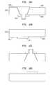
- FIG. 7Dis a sectional view illustrating a variation of the embodiment of FIGS. 2 , 3 and 7 A in which the recesses are provided as thinned regions adjacent edges of a semiconductor chip.
- FIG. 7Eis a plan view illustrating a conductive via extending through a bond pad in accordance with a particular embodiment of a stacked package of FIG. 3 .
- FIG. 8diagrammatically illustrates a first embodiment of a process for fabricating a die stacked package as illustrated herein.
- FIG. 9diagrammatically illustrates a second embodiment of a process for fabricating a die stacked package as illustrated herein.
- FIGS. 10A , 10 B, 10 C and 10 Dillustrate plan and sectional views of a die stacked packages each containing three die having different areas and different locations within the die stacked package with respect to a center line of the package.
- FIGS. 11A and 11Bis a flow diagram of the basic fabrication subprocesses used to produce the die stacked packages of FIGS. 2-7 .
- FIGS. 12A-Dillustrate stages in processing according to the sub-processes of FIG. 11A .
- FIGS. 13A-Cillustrate stages in processing according to the sub-processes of FIG. 11A .
- FIGS. 14A-Dillustrate stages in processing according to the sub-processes of FIG. 11B .
- FIGS. 15A-Cillustrate stages in processing according to the sub-processes of FIG. 11B .
- FIG. 16is a cross-sectional view of a single die stacked package of the type shown in FIG. 2 without a support plate.
- FIG. 17is a cross-sectional view of a single die stacked package of the type shown in FIG. 3 but including a microelectronic element comprising a cavity over part of the die area as the first layer of the stack.
- FIGS. 18A , 18 B, 18 C and 18 Dschematically illustrate further embodiments in which the microelectronic elements in a die stack layer and redistribution layers may be occur in different orientations with respect to a support plate.
- FIGS. 19A-Dshow four permutations of an extended ⁇ RT contact being used to create an electrical pathway between two or more planes possessing electrical conductivity.
- FIGS. 20A through 20Hillustrate stages in a wafer-level process of fabricating microelectronic packages having a plurality of die stacked therein.
- FIG. 20Iis a sectional view illustrating formation of a recess in a process of forming a microelectronic package in a particular embodiment.
- FIGS. 21A-21Eare sectional views illustrating a process of fabricating microelectronic packages in accordance with a particular embodiment.
- FIGS. 22A-22Care sectional views illustrating a variation of the process shown in FIGS. 21A-E .
- FIGS. 23A-Care sectional views illustrating a process of fabricating microelectronic packages containing a plurality of stacked die therein in accordance with a particular embodiment.
- FIG. 24Ais a sectional view illustrating a variation of the process shown in FIGS. 23A-C .
- FIG. 24Bis a plan view corresponding to the sectional view of FIG. 24A .
- FIGS. 25A-Care a sectional view and corresponding plan views of a multiple die package and a wafer containing sets of die for making multiple die packages, in accordance with a particular embodiment.
- FIGS. 26A-Hare sectional views illustrating stages in fabrication of a microelectronic package in accordance with a particular embodiment.
- a contact, bond pad or other conductive element “exposed at” a surface of a dielectric elementmay be flush with such surface; recessed relative to such surface; or protruding from such surface, so long as the contact, bond pad, or other conductive element is accessible by a theoretical point moving towards the surface in a direction perpendicular to the surface.
- a “die stacked package”is a single microelectronic package containing multiple microelectronic elements (for example, semiconductor chips or die) within the package. This is in contrast to a “stacked die package” which is defined herein as a stack of individually packaged microelectronic elements.
- a “stacked die package”is an assembly including a plurality of individual packages containing microelectronic elements are joined together in a stack, in which external terminals of at least one packaged microelectronic element are electrically connected with the external terminals of at least one other packaged microelectronic element.
- FIGS. 1A and 1Billustrate the difference between a die stacked package and a stacked die package. Note that details such as electrical connections between or among individual die and between a microelectronic package and other packages or substrates are omitted for purposes of illustration.
- die stacked package 100is a single entity that contains by way of example three die, 101 , 102 and 103 arranged vertically one on top of another surrounded by unitary enclosure 104 .
- the die stacked packagecan have an encapsulant or other structure protecting the microelectronic elements as a unit, and typically has a set of terminals (not shown) exposed at an exterior of the package through which electrical connections can be made to the microelectronic elements within the package.
- the example of three die shown in FIG. 1Ais not intended to be limiting in any way; fewer or more die may be stacked in this manner.
- FIG. 1Billustrates a stacked die package 150 i.e., an assembly containing a plurality of stacked and electrically connected packages, constructed from three discrete chip scale packages 110 , 120 and 130 . Each discrete chip scale package is surrounded by unitary enclosure 152 .
- chip scale package 120is shown stacked and affixed by material 151 to chip scale package 130
- chip scale package 110is shown stacked and affixed by material 151 to chip scale package 120 to collectively form the assembly of individual packages which make up the stacked die package 150 . It can be seen from FIG. 1B that any number of discrete chip scale packages may be stacked in this manner.
- FIG. 1Bany number of discrete chip scale packages may be stacked in this manner.
- each discrete chip scale package 110 , 120 and 130happens to contain a single die, 111 , 121 and 131 respectively, but the term stacked die package as used herein is not limited to such an arrangement; each discrete chip scale package 110 , 120 and 130 could also contain multiple die such as die stacked package 100 .
- Die stacked package 100may result in a physically more compact component because less material is used to form the package enclosure.
- Stacked die package 150when each discrete chip scale package contains a single die, may provide higher functional yield because each die may be fully tested as a functioning die (the concept referred to as “known good die”) before committing the tested package to the stack.
- FIG. 2is a perspective view of a first embodiment of a die stacked package 200 as viewed from a first surface that is referred to herein as upper surface 201 .
- Die stacked package 200has oppositely facing, generally planar upper surface 201 and lower surface 202 ; lower surface 202 is not visible in this view.
- Edge surfaces 206extend between the upper and lower surfaces 201 , 202 . At least some of the edge surfaces 206 can extend between the lower and upper surfaces at an inclined angle such that upper surface 201 can have smaller area than lower surface 202 .
- the inclined anglecan be about 30 degrees from the perpendicular with respect to the lower surface. In a particular embodiment, the angle can range from 5 degrees to 40 degrees. The angle can be smaller or larger as necessary up to the physical limits of between 0 degrees from the perpendicular and 89.9 degrees.
- the dimensions of die stacked package 200may be determined by the contents of the package (e.g., the number of die stacked, the height of each stacked die, etc.), and thus may vary greatly. In one embodiment, the package dimensions can be several to tens of millimeters on a side, i.e., the length of the edge surface 206 where it meets the lower surface 202 of the package 200 . In one embodiment, the die stacked package 200 is from less than a millimeter to just a few millimeters in height h, giving the package 200 the aspect ratio of a plate.
- Die stacked package 200has the capability to make electrical connection to other components.
- electrical connection to other componentscan be made through a ball grid array (BGA) interface 203 on upper face 201 .
- BGAball grid array
- a BGA interfacecan contain an array of partial spheres 205 of solder exposed at an exterior face of the package 200 .
- By suitable processingit is possible to simultaneously physically attach and electrically connect the spheres of the BGA interface of an electronic component such as die stack package 200 to corresponding terminals of a printed circuit board, or atop another substrate or component.
- Other embodiments of die stack package 200 not shown heremay make use of a variety of other connection schemes in place of a BGA interface 203 that are well known to those skilled in the art, such as wire bonding and TAB (tape automated bonding).
- BGA interface 203can be connected to other parts of the package by a redistribution layer (RDL) including conductive elements or conductive traces 204 .
- the traces 204can extend from terminals (not shown) underlying in alignment with the solder spheres of the BGA along the upper surface 201 and onto the edges, i.e., edge surfaces 206 of the package.
- the traces 204have high aspect ratio; that is, each trace typically has a length 208 and a breadth (width) 209 much greater than the thickness of the trace extending in direction above surface 201 . While traces 204 in FIG. 2 appears as a relatively uniform pattern of straight conductive areas, traces may also appear in less uniform patterns and may even have a serpentine appearance.
- FIG. 3is a perspective view of a second embodiment of a die stacked package 220 .
- Die stacked package 220has a generally planar upper surface 221 and lower support structure 228 ; lower support structure 228 has lower surface 222 which oppositely faces upper surface 221 .
- Die stacked package 220is shown as viewed from upper surface 221 in FIG. 3 .
- lower support structure 228extends slightly beyond the edge surfaces 206 .
- Traces 224extend onto the upper face 210 of lower support structure 228 that extends slightly past edges 206 .
- FIG. 4is a perspective view of a third embodiment of a die stacked package 230 .
- Die stacked package 230has oppositely facing, generally planar upper surface 231 and lower surface 232 , and is shown as viewed from upper surface 231 in FIG. 4 .
- BGA interface 233is visible on upper surface 231 . While the traces 204 of the RDL in FIGS. 2 and 3 appears as a relatively uniform pattern of straight conductive areas, an RDL may also appear in less uniform patterns and may even have a serpentine appearance.
- FIG. 4is a perspective view of a third embodiment of a die stacked package 230 .
- Die stacked package 230has oppositely facing, generally planar upper surface 231 and lower surface 232 , and is shown as viewed from upper surface 231 in FIG. 4 .
- BGA interface 233is visible on upper surface 231 . While the traces 204 of the RDL in FIGS. 2 and 3 appears as a relatively uniform pattern of straight conductive areas, an RDL may
- FIG. 4illustrates an example of an RDL that is asymmetrical in appearance with respect to the pattern that appears on top surface 231 of package 230 , such that some traces 234 are longer than other traces and the pattern of traces may not be the same on all edge surfaces 236 of the package.
- FIG. 5is a plan view of a fourth embodiment of a die stacked package 240 , as viewed from a generally planar upper surface 241 . An oppositely facing lower surface of die stacked package 240 is not visible in FIG. 5 .
- RDL 244 in FIG. 5illustrates an example of a redistribution layer that is symmetrical in appearance with respect to the pattern that appears on top surface 241 and on the edge surfaces 246 and 247 of package 240 .
- FIG. 6is a plan view looking towards edge surface 247 of die stacked package 240 of FIG. 6 .
- FIG. 6shows that upper surface 241 is smaller in area than the lower surface 242 . As seen in FIGS.
- the upper and lower surfaces 241 , 242are connected by planar edge surface 247 which extends at an inclined angle relative thereto.
- BGA interface 243is visible on upper surface 241 of die stacked package 240
- traces 244 of the RDLare visible on the package edge surface 247 .
- FIG. 7Ais a cross-sectional view of die stacked package 220 of FIG. 3 taken at line A of FIG. 3 .
- the cross-sectional view of FIG. 7Ais not necessarily drawn to the same scale as shown in FIG. 3 ; some structures in the cross-sectional view of FIG. 7 may be shown as being larger relative to other structures in the view in order to more clearly show the interior features of die stacked package 220 .
- Lower support structure 228forms the base of package 220 .
- the exterior of die stacked package 220may not reveal the number of die that are stacked within the package.
- three die 101 , 102 and 103are stacked in a “face down” orientation. That is, the surface of each die on which bond pads 603 and 604 or other metallic pads of the die are disposed is closest to the support plate 228 . Note that in the embodiment shown in FIG. 7A , there is a single die on each level of package 220 that appears to be in three distinct fragments or portions, as indicated by the use of identical cross-hatching. This fragmented die structure is explained in more detail below.
- a first die 101is shown attached to lower support plate 228 by a dielectric material 602 ; first die 101 is surrounded by dielectric material 602 which allows for second die 102 and third die 103 to be similarly stacked and attached in a vertical direction, one above the other.
- a front face 606 of the second die 102can be adjacent a rear face 608 of the first die 101
- a front face 606 of the third die 103can be adjacent a rear face 608 of the second die 102 .
- bond pads or other metallic pads 603 and 604are exposed at a front surface 606 of each of the first, second and third dies 101 , 102 , 103 .
- the metallic pads 603 , 604can be electrically connected with microelectronic devices, e.g., semiconductor devices, of each respective die.
- Recesses 618can extend from the rear surfaces 608 of the die 101 , 102 , 103 toward the front surfaces 606 .
- Examples of the shapes the recesses can haveare: cylindrical, frusto-conical, or pyramidal, to name a few.
- Walls 622 of the recessescan be oriented in a normal direction to the front surface 606 , or can be oriented at an angle 621 away from the normal.
- walls 622 of the recess 618can be oriented at an angle 621 of about 5 degrees or greater with respect to a normal to the rear surface.
- the wallscan be oriented at an angle of less than or equal to about 40 degrees with respect to a normal to the rear surface.
- Recesses 618can be provided such that each recess in a particular die is aligned with a single bond pad of that die.
- a statement that one element is “aligned” with another element underlying such elementshall mean that the two elements are “at least approximately aligned” such that there is at least one line which passes through the one element and the underlying element in a direction perpendicular to a surface of the one element.
- each recesscan be formed such that the width of the recess is uniform in lateral directions in the plane of the front surface 606 .
- the walls 622 of a recesscan be vertical, i.e., in a normal direction 607 to the front surface 606 of the die.
- the recesscan be tapered, becoming smaller with increasing distance from the rear surface.
- the width of the recess 618 at the rear surface 608can be quite larger than the width 630 of the recess which is adjacent the bond pad 604 .
- a portion of metallic pads 603 and 604has been removed and conductive vias 605 through the bond pads, i.e., completely through a thickness of the bond pads.
- a statement that a conductive via extends “through a bond pad,” or “through a metallic pad” of a microelectronic elementshall mean that the metallic material of the via extends completely through a thickness of such bond pad or metallic pad from a rear surface of the pad to a front surface of the pad.
- At least a portion of a bond pad or a metallic pad of a microelectronic elementhas a thickness extending in a direction away from a surface of such microelectronic element and has lateral dimensions which extend in directions 628 along such surface which typically are substantially larger than the thickness.
- Each conductive via 605typically directly contacts a surface 640 of the bond pad 604 exposed by the hole that extends through the bond pad thickness.
- Conductive viasare electrically connected with a conductive layer 610 , e.g., a layer including or consisting essentially of metal, which extends along a wall 622 of the recess and being insulated from the wall by a dielectric layer 623 .
- the dielectric layer 623is relatively thin, and can extend conformally along the walls 622 of the recess and onto the rear surface 608 of each die.
- the conductive layercan be further connected to a conductive trace 635 which extends along the die rear surface 608 and along a surface 634 of a dielectric layer 636 extending away from edges 620 of the die.
- a plurality of leadse.g., traces 224 of RDL can extend along the sloping edge surfaces 206 of package 220 and onto upper surface 221 of the package to terminals 616 which are exposed at such surface 221 , on which solder spheres or bumps of the BGA interface 203 can be attached.
- the edge surface 206can extend along the edges 620 of the die within the package.
- Interior to die stack package 220is a conductive layer including conductive traces 610 which provide an electrical pathway between the leads 224 at the exterior of the package 220 and respective bond pads 603 and 604 . Trace 610 is represented as a thick black line in the interior of package 220 .
- traces 610may be connected with a single external lead 224 , or only one trace 610 may be connected with each external lead 224 .
- Circle 612 in FIG. 7Ashows electrical connection 614 which connects wiring trace 610 to redistribution layer 224 .
- Electrical connection 614may be referred to as an “edge connection” because it is the sectional surface, or edge, of wiring trace 610 that is in contact with redistribution layer 224 .
- Electrical connection 614may also be referred to as a “T contact” connection because it can be seen that the portion of wiring trace 610 and leads 224 shown in circle 612 together form the shape of the letter T.
- conductive vias 605can extend through respective metallic pads 603 and 604 .
- a conductive via 625can be completely enclosed within the area of a metallic pad 604 .
- FIG. 7Badditionally illustrates dielectric layer 623 which is disposed laterally outward from the conductive via.
- Each dieincludes recesses 618 which extend from the rear surface 608 of die towards the front surface 606 .
- the conductive layere.g., trace 610 , connects to the conductive via and extends along a wall 622 of the recess and along the rear surface 608 of the die towards an edge 620 of the die.
- the arrangement and fabrication of the recesses 618 , conductive vias 605 , and conductive layer 610 connected thereto to provide electrical connection between the bond pads at the front surface and the conductive layer at the rear surface of a particular diecan be as described below.
- the recessescan be formed by various means for removing semiconductor material from the rear surface 608 .
- the recessmay expose a portion of a major surface 624 of the metallic pad 603 or 604 which is not ordinarily exposed because it faces inwardly towards an interior of the die. However, in a particular embodiment, the surface 624 of the metallic pad may not become exposed as a result of forming the recess.
- the recesscan have a base 626 which extends in a direction in which the front surface 606 of the die extends.
- the width 630 of the base 626 in that direction 628can be greater than the width 632 of the conductive via 605 in the same direction 628 .
- An opening or “void”can be made, e.g., by drilling, which extends through the full thickness of each bond pad 603 and 604 on a single die and some distance into the dielectric layer 602 adjacent the front surface.
- a metal layercan then be deposited by a process applied in a direction from the rear surface 608 to form the conductive via 605 .
- trace 610 connected to the via 605can be formed simultaneously by the same deposition process. In such case, the portion of the metal layer which forms the via 605 in contact with bond pad 603 or 604 and deposited in the void during fabrication may be viewed as contact 605 .
- the metal layercan extend from the via 605 conformally along a surface 622 of the recess 618 .
- the dielectric layer 602may overlie the conductive layer 610 within the recess 618 .
- dielectric layerscan have surfaces 634 which extend beyond the edges 620 of the dies. In such case, the conductive layers 610 can extend in direction 628 along surfaces of the dielectric layers 634 beyond the edges 620 of the dies.
- the contact 605need not have the substantially rectangular shape shown in the cross-sectional view of FIG. 7A , and that the shape of the void produced during fabrication will depend on the technique used to penetrate the bond pads.
- contact 605may be a radially symmetric “T contact” of the type discussed above, and when that embodiment is used, it is referred to herein as a “micro-RT contact” or “ ⁇ RT contact.”
- a contact 605can be made at each bond pad in die stacked package 220 ; as with wiring trace 610 , not all instances of contact 605 are called out with a reference number in FIG. 7A .
- a recess 619 ( FIG. 7C ) in a diecan extend as a trench in a direction into and out of the plane of the drawing which is represented in FIG. 7A .
- a plurality of bond pads 603 of the same diecan be aligned within the same recess 619 in that die.
- a recess of a dieis formed as a thinned portion 619 ′ of the semiconductor region of the die 101 ′ aligned with the bond pads 604 , wherein the thinned portions of the semiconductor region extend to edges 620 of the die.
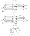
- a conductive via 640( FIG. 7E ) extending through at least the partial area of more than one metallic pad 613 on a die can be used to electrically connect the metallic pads with traces extending to other locations on an assembly.
- such conductive via 640could be used to electrically connect the pads 613 together for distribution of power or ground to other locations on the assembly.
- fabrication process 800constructs a die stacked package 820 by making a vertical assembly of two or more die 801 which includes electrically conductive elements, e.g., traces, etc., exposed at an exterior of each die, and providing encapsulation 812 and electrically conductive elements 816 for connecting the die to terminals 814 of the final package.
- electrically conductive elementse.g., traces, etc.
- FIG. 9is a simplified schematic illustration of Wafer Level Packaging (WLP) process 900 .
- Wafer Level Packagingis a chipscale packaging (CSP) technology in which steps of packaging microelectronic elements are performed simultaneously as to a plurality of microelectronic elements 801 which, for example, are attached together at dicing lanes 904 in form of a wafer or portion of a wafer.
- CSPchipscale packaging
- Wafer Level Packagingcan also refer to packaging of microelectronic elements performed simultaneously as to a plurality of microelectronic elements 801 which have been previously severed from a wafer but which are attached together at edges 904 of each microelectronic element in form of a reconstituted wafer with a material, e.g., adhesive, holding the microelectronic elements in position.
- a materiale.g., adhesive
- consecutive individual wafers of die from among two or more wafers 910 , 911 and 912 of die 801are each subjected to fabrication processes that prepare each wafer for alignment and stacking into multi-layer wafer stack 930 .
- each waferis encapsulated and provided with terminations while still in wafer form.
- Cutting through multi-layer wafer stack 930 in a direction along the dicing lanes 904frees individual packages 820 , each of which can be fully encapsulated with material 812 and provided with conductive elements 824 and an external electrically conductive interface, such as, for example, ball grid array 803 , for attaching package 820 to another component or to a substrate such as a PCB substrate.
- the die in each layerare effectively constrained to being all of the same type; their area dimensions and array spacing must substantially exactly match with each the area and dimensions of die on other ones of the wafers that are to be stacked.
- the yield of working die on each wafermay vary, and if one die in each of the packages 820 is not working, the overall yield of a fully working die stacked package 820 may be unacceptably low.
- Compound yieldis the final yield when a number of wafers of die are stacked where each layer has a certain yield.
- the final yield in a three layer stackis 60% for the first layer, 90% for the second layer and 98% for the third layer the final yield will be 52%, which may not be economically viable. However if each layer in a three layer stack has 98% yield, the final yield is more acceptable at 94%.
- One approach to ensure that the fabrication process produces a high yield of die stacked packagesis to build each wafer layer in a stack of wafers from individual die that have passed a degree of testing and are known good die.
- Known good diemay be separated from their original wafer(s), before or after individual testing, and inferior, non-working die may be discarded. Then, the known good die are re-assembled onto a wafer-like substrate in order to take advantage of a wafer level assembly process such as fabrication process 900 of FIG. 9 .
- a wafer-like substrate on which known good die are mounted in an array formatis referred to as a reconstituted wafer.
- the wafer-like substrate that supports the known good die array assemblymay also serve as a base layer, such as lower support structure 228 of FIGS. 3 and 7 .
- the base layer or support plateis shaped to match the external dimensions of a semiconductor wafer so that it can be handled easily by equipment used to perform wafer level packaging steps thereon with die-containing wafers, as described below.
- a suitable part to use for the support platecan be a reclaimed silicon wafer having the same diameter (e.g., 200 mm or 300 mm) as the die-containing wafers.
- the base layercan consist essentially of a material, e.g., glass, quartz, or other inorganic dielectric material, which has a relatively low coefficient of thermal expansion and relatively high Young's modulus, so that the dimensions of the base layer during processing remain stable with respect to the die-containing wafers, and also provides electrical insulation.
- the thickness of the base layerwill be about 750 micrometers (also referred to as microns or “ ⁇ m” herein).
- the support platecan either remain a permanent part of the final die stacked package (see e.g., die stacked package 220 of FIGS. 3 and 7 ) or removed and recycled.
- the support plateallows the spacing between die to be maximized for die manufacture and also set at a convenient value for the packaging process.
- the dicing lanes between the dieprovide a die-to-die spacing of typically 50 ⁇ m or less.
- the spacing between adjacent diecan range 100-300 ⁇ m, for example.
- Another advantage of building each layer of the die stacked package using individual die bonded to the support plateis that the individual die that are ultimately packaged into the die stacked package can be obtained from multiple and different sources; that is, the individual die may be obtained from different wafers, from different suppliers and even originate from wafers that have different dimensions.
- semiconductor manufacturersendeavor to use the largest possible diameter of wafer.
- wafer level packaging equipmentable to handle the very largest semiconductor wafers may be unavailable or prohibitively expensive.
- the diameter and thickness of the semiconductor wafer from which the original die are sourcedare decoupled from the diameter of the support plate used for the wafer level packaging process and the thickness of each layer in the die stacked package.
- the support platecan have a smaller diameter than the diameter of the original wafer.
- the support platemight even be rectangular shape, such that, in one embodiment, the die can be arranged in an array having the same number of die in each row.
- FIGS. 10A , 10 B, 10 C and 100This advantage of flexibility in die size and location is schematically illustrated in FIGS. 10A , 10 B, 10 C and 100 .
- die 101 , 102 and 103are shown as being the same size and centered around center line 108 relative to each other within package 100 .
- FIG. 10Aschematically illustrates die stacked package 720 in which the plan area dimensions of die 701 , 702 and 703 differ from each other; in FIG. 10A , die 701 , 702 and 703 are centered on die pitch center line 708 .
- FIG. 10Aschematically illustrates die stacked package 720 in which the plan area dimensions of die 701 , 702 and 703 differ from each other; in FIG. 10A , die 701 , 702 and 703 are centered on die pitch center line 708 .
- FIG. 10Aschematically illustrates die stacked package 720 in which the plan area dimensions of die 701 , 702 and 703 differ from each other; in FIG.
- FIG. 10Bis a schematic plan view of the relative size and orientation of die 701 , 702 and 703 of FIG. 10A .
- FIG. 10Cschematically illustrates die stacked package 730 in which the plan area dimensions of die 711 , 712 and 713 differ from each other; in FIG. 10C , die 711 , 712 and 713 are not centered on die pitch center line 708 .
- FIG. 100is a schematic plan view of the relative size and orientation of die 711 , 712 and 713 of FIG. 10C . Because die 712 is larger than die 713 , it is wholly obscured in this view and is represented by dotted line shape 712 .
- FIGS. 11A and 11Bis a flow diagram 1000 of the basic fabrication subprocesses used to produce die stacked packages 200 , 220 , 230 and 240 of FIGS. 2-7 .
- the fabrication processes illustrated in FIGS. 11A and 11Bmay be carried out as a Wafer Level Packaging (WLP) process.
- WLPWafer Level Packaging
- the fabrication processes illustrated in FIGS. 11A AND 11 Bare discussed herein in conjunction with FIGS. 12 through 15 .
- fabrication process 1000 of a die stacked packagebegins with sub-processes 1010 through 1030 of building a first reconstituted wafer.
- a suitable support plate 1210FIG. 12A ) upon which to build a reconstituted wafer comprising an array of individual die is sourced and prepared.
- the area of the support plateis populated in sub-process 1020 with a planar array of tested die 1230 (also referred to as a die layer) in a face-down orientation ( FIGS.
- subprocess 1016is a representative technique of using a die attach adhesive 1212 .
- a dielectric layer 1240is applied over the microelectronic elements 1230 of the die layer in sub-process 1026 , filling in the areas between microelectronic elements 1230 ; dielectric layer 1240 may also cover the rear faces 1232 of microelectronic elements 1230 .
- the dielectric layercan include one or more inorganic dielectric materials such as an oxide, nitride, which may include silicon dioxide, silicon nitride or other dielectric compound of silicon such as SiCOH, among others, or may include an organic dielectric, among which are various polymers such as epoxy, polyimide, among others. As seen in FIG.
- each microelectronic elementcan then be reduced in sub-process 1030 by lapping, grinding or polishing the structure from the rear faces 1232 of each microelectronic element 1230 .
- the thicknessis reduced to 50 to 100 micrometers.
- Sub-process 1030produces thinned reconstituted wafer structure 1250 .
- sub-process 1034forms recesses 1252 ( FIG. 13B ) extending from the rear surfaces 1216 of the die towards the front surfaces 1218 .
- the recesses 1252can be tapered such that they have larger width at the rear surface 1216 than locations of the recesses adjacent to the front surface.
- the recessesmay extend entirely through the silicon portion of the die of the thinned reconstituted wafer structure 1250 ( FIG. 13A ). Vias 1252 are opened at the location of and to the depth of the bond pads on each microelectronic element in structure 1250 using any suitable drilling technique.
- Sub-process 1034produces reconstituted wafer structure 1254 ( FIG. 13B ).
- a dielectric layer 1258( FIG. 13C ) is applied over reconstituted wafer structure 1254 , which can conformally coat the microelectronic elements including interior surfaces of the recesses therein to produce structure 1256 .
- voids 1262e.g., blind holes are formed by drilling through the bond pads of the individual microelectronic elements of structure 1256 . Laser drilling is one suitable technique to use to form voids 1262 .
- Sub-process 1054produces reconstituted wafer structure 1260 . ( FIG. 14A )
- a metal layer 1262( FIG. 14B ) can be formed onto exposed surfaces within the voids 1262 , the recesses 1252 and overlying the rear surface 1216 to form the structure 1266 illustrated.
- the formed metal layer 1262can include conductive vias within the voids and traces which extend from each conductive via along a surface of the recess and to locations overlying the rear surface 1216 of each die.
- the metal layercan be considered a “redistribution layer” as described above and as indicated in subprocess 1060 ; it provides conductive connection between the bond pads and the traces overlying the rear surface.
- the metal layercan be formed, for example, by forming a conductive seed layer by sputtering or electroless plating, for example, then photolithographically patterning the seed layer, and then electroplating a metal layer onto the conductive seed layer.
- the seed layercan serve as an electrical commoning layer during the electroplating step.
- a dielectric material 1272( FIG. 14C ) can be deposited to cover the die with the metal layer thereon to form the structure 1270 .
- another layer of diecan be arranged on the dielectric layer 1272 and bonded thereto with a die attach adhesive, and then the subprocesses 1026 , 1030 , 1034 , 1050 , 1054 , 1060 , 1066 ( FIGS. 11A-B ) can be repeated to form a second substructure 1284 ( FIG.
- a stacked assembly 1280containing a plurality of die attached together at edges and vertically stacked with the front faces 1218 of the die of the upper layer 1284 facing the rear faces 1216 of the lower layer of the die.
- one or more additional layers of die(not shown) having recesses and conductive vias and layers thereon can be formed by the above-described subprocesses.
- a plurality of taper slotsi.e., trenches can be formed which extend in a downward direction away from a top surface 1284 of the dielectric layer 1272 of the stacked assembly 1280 and along edges 1222 of the die.
- the trenchescan also extend in a direction laterally along a surface 1211 of the support plate.
- the trenches 1282can fully separate all the die in one vertical stack 1288 A from all the die in another vertical stack 1288 B.
- the trenchescan be tapered such that the width 1286 of each trench becomes smaller in a downward direction extending towards the support plate 1210 .
- the trenchescan be formed by a dicing subprocess, such as by using a saw to form a tapered trench between edges 1222 of adjacent die.
- the traces connected to the bond pads of each diecan be exposed at interior surfaces 1224 of the trenches.
- conductive leads of an RDLcan be formed which are electrically connected with the exposed traces 1262 .
- the leadscan be formed, for example, by a process including electroplating, similar to the process by which the conductive vias and conductive traces connected to each die are formed.
- a three-dimensional lithography processis used to form the leads 1290 , such as described, for example, in U.S. Pat. No. 5,716,759, the disclosure of which is incorporated by reference herein.
- the leads 1290can extend onto a face 1292 of each assembly and can be electrically connected with terminals 1294 exposed at the face.
- solder bumps or spherescan be bonded to the terminals 1294 to form a BGA interface 1280 ( FIG. 15C ) for connecting the terminals of the stacked assembly to another element, for example, a circuit panel.
- individual stacked assembliescan be severed from each other, such as by dicing, to form the stacked assembly, e.g., die stacked package 1600 seen in FIG. 16 .
- the subprocesses 1 through 9can be performed to provide individual subassemblies, each containing a support plate, a layer of die thereon, and conductive vias, and redistribution layer thereon, as described above.
- the subassembliescan then be stacked and joined together with the support plates between adjacent ones of the subassemblies optionally removed.
- the subprocesses 12 through 15can be performed to create a plurality of microelectronic assemblies as shown and described above, e.g., FIG. 7A ).
- FIG. 17is a cross-sectional view of an embodiment of die stacked package 1700 in which the microelectronic element 1701 closest to support plate 1710 in die stacked package 1700 is positioned adjacent a cavity 1720 .
- the cavitymay be needed to support the function of a microelectromechanical system (“MEMs”) device such as, for example, an accelerometer or a surface acoustic wave (“SAW”) filter.
- MEMS devicesmicroelectromechanical system
- SAWsurface acoustic wave
- Many types of MEMS devicesrequire a sealed gas or vacuum cavity over part of the die area for their function, performance, longevity or assembly.
- the cavitymay be evacuated or filled with gas or liquid in accordance with known practice for such devices.
- Other types of microelectronic devices, such as, for example, a solid state image sensorcan require a cavity to permit focusing of an image onto a surface of the image sensor.
- the support plateis preferably a borosilicate glass which is transparent and has a coefficient of thermal expansion match which is close to that of the die material.
- the glass waferwill typically range from 100 to 300 micrometers in thickness, but could be as thin as 25 micrometers or could be several millimeters in thickness. Glass can be selected on account of the optic functionality of the image sensor.
- process 1000varies from the above description when microelectronic element 1701 is the first die layer.
- An array of microelectronic elements 1701are attached to support plate 1710 by die attach material 1702 ; die attach material 1702 is prevented from covering the entire front surface area of the die by sidewall material 1730 , which leaves cavity 1720 over front surface area of each die.
- FIGS. 18A , 188 , 18 C and 18 Dschematically illustrate further embodiments in which the microelectronic elements in a die stack layer may be mounted in different orientations, and in which redistribution layers occur at different positions in the die stack package.
- the support plate(such as support plate 1210 of FIG. 12 ) is not shown in the figure but it is assumed to be below the structure illustrated in the figure.
- FIG. 18Ashows die 1803 in face-down orientation such that bond pad 1803 on the front face 1801 of the die is towards the support plate.
- RDL 1804is on the rear face 1802 of the die.
- FIG. 188shows die 1810 also in a face down orientation relative to the support plate; RDL layer 1814 is on front face 1811 of die 1810 .
- FIG. 18Cshows the die in face up orientation where the RDL is on the bottom face of the die.
- FIG. 18Dshows the die in face up orientation where the RDL is on the front face of the die. Where required, die could simultaneously have both a front face redistribution layer and ⁇ RT contacts to the rear face.
- RDLhas been shown in the configuration where one RDL is associated with each layer of die in the stack. It is possible there is a requirement for RDLs in other layers of the stack. These may be independent structures unassociated with a die layer or a die layer may have several RDLs.
- FIGS. 19A , 198 , 19 C and 19 Dshow several further embodiments of the structure where direct contact can be made between wiring traces, lands and bond pads on multiple layers by using a ⁇ RT contact.
- the near-parallel sided portion of the ⁇ RT contact 1901which normally only extends through one RDL 1904 is shown extended to penetrate through a second RDL 1902 .
- the near-parallel sided portion of the ⁇ RT contactextends through a first RDL but terminates on the surface of a second RDL 1902 , joining to it at interface 1903 .
- FIG. 19Ctwo RDL layers are shown as being joined at interface 1904 with both RDLs being penetrated by the ⁇ RT contact.
- FIG. 19Dshows a larger portion of a ⁇ RT contact with both the near-parallel sided portion 1901 and its continuation 1905 up an inclined surface.
- the near-parallel sided portion 1901connects to RDL 1904 by penetration while the inclined continuations of the ⁇ RT contact intersect other RDLs 1906,1907 and 1908, forming T-style contacts at the intersections.
- FIG. 19Athe extended ⁇ RT contact connects two layers by penetrating through the thickness of both.
- FIG. 198the extended ⁇ RT contact connects two layers by penetrating the upper layer and terminating on the second.
- FIG. 19Cthe extended ⁇ RT contact penetrates through the thickness of a Shellcase L-style contact, which is a joint between one layer superimposed on another.
- FIG. 19Dshows several layers connecting to the redistribution layer (RDL) above a ⁇ RT contact.
- RDLredistribution layer
- the processbegins with a plurality of die, e.g., of silicon or other material, which remain attached together at edges 2002 thereof in form of an intact wafer 2000 or portion of a such wafer, wherein dicing lanes 2004 of the wafer extend between the edges 2002 of adjacent die 2001 .
- the waferthen is attached to the support plate or permanent carrier 2010 , e.g., by an adhesive, with the bond pads 2003 on the front face 2006 of the wafer adjacent to the support plate.
- the wafer 2000is thinned by polishing or grinding or other processing from a rear face 2008 thereof, as shown at 2020 .
- recesses 2024 , 2026are formed which extend from the rear surface 2008 of the wafer towards the front surface 2006 .
- Recesses 2024are formed in alignment with bond pads 2003 of the wafer.
- other recesses 2026can be formed in alignment with the dicing lanes 2004 of the wafer.
- the recesses 2024can extend completely through the thickness of the portion 2030 of the wafer that consists essentially of monocrystalline semiconductor material as a bulk semiconductor region of the wafer.
- the recesses 2024may have an interior surface exposing a surface 2032 of a dielectric layer 2034 underlying the bond pad.
- the recesses 2024can be formed by etching, drilling (e.g., laser ablation or mechanical drilling) or otherwise removing the semiconductor material of the wafer until the surface of the dielectric layer 2034 is exposed. The etching process can then be stopped. In one embodiment, the removal process can be endpointed when the surface 2032 of the dielectric layer is exposed.
- the removal processcan be performed by an etching process, and the etching process can be performed selectively with respect to the material of the underlying dielectric layer 2034 , the bond pad 2003 , or both.
- This processcan also apply to any of the foregoing and any of the following described embodiments.
- Recesses 2026typically are formed simultaneously with recesses 2024 and can have a similar structure, except that recesses 2026 are not required to be aligned with bond pads. Recesses 2026 can also extend completely through the thickness 2028 of the monocrystalline semiconductor portion of the wafer. In a particular embodiment, when the wafer has a silicon-on-insulator (SOI) structure, the recesses can extend completely through the bulk semiconductor region, a buried oxide (BOX) layer and the monocrystalline silicon-on-insulator layer that overlies the BOX layer. In one variation, the recesses can extend through the dielectric layer 2034 as well, such that a rear surface 2013 of the bond pad 2003 is exposed within the recess.
- SOIsilicon-on-insulator
- BOXburied oxide
- the recessescan extend through the dielectric layer 2034 as well, such that a rear surface 2013 of the bond pad 2003 is exposed within the recess.
- FIGS. 20D , 20 E, 20 F, 20 G and 20 Hrespectively, the processing described above with respect to FIGS. 11A-16 is applied to structure seen at 2022 .
- a conformal dielectric layer 2058 or “passivation layer”can be applied to the exposed surfaces of the recesses, after which, the voids 2062 in the bond pads 2003 can be formed ( FIG. 20E ), and then a metal layer ( FIG. 20F ) including the conductive vias extending through the bond pads, and the traces 2062 can be formed.
- a dielectric layer 2066then can be formed which covers the rear surfaces of the die 2001 including the metal layer 2062 thereon within the recesses 2024 and the recesses 2026 .
- FIGS. 20B-20Gcan then be repeated after attaching to the dielectric layer 2066 a second intact wafer or portion of an intact wafer in which the die thereon remain attached together at dicing lanes 2004 of the wafer, as described above relative to FIG. 20A to form a second layer 2068 of die having the structure as illustrated in FIG. 20G .
- This processingcan then be repeated again to form third and fourth layers 2072 , 2074 of die, or any number of layers of die in a stacked assembly as seen in FIG. 20G . Referring to FIG.
- a dicing operationcan be performed to form notches or trenches in the stacked assembly 2090 which extend in a direction from the highest layer 2074 of die downwardly toward the support layer 2010 , the notches extending through the recesses 2026 formed earlier in each wafer along the dicing lanes therein.
- further processing to form leads, a BGA interface, and final dicing into individual assemblies, e.g., die stacked packagescan be performed, as described in the foregoing with respect to FIGS. 15B and C.
- the variations described above with respect to FIG. 16 or FIG. 17 or FIGS. 18A through 19Dcan also be applied here.
- individual microelectronic elements or die 2101can be mounted face-down onto a substrate 2110 having wiring patterns 2120 thereon, with an adhesive 2102 bonding the front faces 2108 of the die to a major surface of the substrate 2110 .
- Bond pads 2014 on the front faces of the diecan be positioned such that they confront corresponding metallic pads or contacts 2114 of the wiring substrate.
- a dielectric material 2122e.g., a polymeric material such as any of the materials used as layer 1240 provided between die in FIG. 12D , can be provided between edges 2124 of adjacent die 2101 .
- the thicknesses of the diecan then be reduced, such as by grinding, lapping or polishing the die from the rear surfaces 2106 thereof.
- recesses 2136as described in one or more of the above-described embodiments can be formed in the die in alignment with the bond pads 2104 .
- a further dielectric layer 2132can then be formed which covers the rear surfaces 2106 of the die and the interior volumes within the recesses.
- the dielectric layercan be similar to the dielectric layer 1272 ( FIG. 14C ) which has a relatively flat major surface on which to provide additional structure, such as seen in FIG. 14 D.
- the dielectric layer 2132can have a self-planarizing property when deposited.
- a polishing processcan be used to planarize the dielectric layer.
- Redistributed conductive elements 2134e.g. pads or traces, of the structure can extend in a lateral direction along the surface of the dielectric layer 2132 above the rear surfaces 2106 of the die.
- the redistributed conductive pads 2134can function as terminals available to connect other elements, e.g., another microelectronic assembly, circuit panel, or other active or passive electrical or electronic device thereto. As seen in FIG. 21D , electrically conductive elements, i.e., vias 2126 are formed which electrically connect the bond pads 2104 with the aligned substrate pads 2114 .
- Redistributed conductive elements 2134e.g. pads or traces, of the structure can extend in a lateral direction along the surface of the dielectric layer 2132 above the rear surfaces 2106 of the die.
- the redistributed conductive pads 2134can function as terminals available to connect other elements, e.g., another microelectronic assembly, circuit panel, or other active or passive electrical or electronic device thereto. As
- the assemblycan be severed, e.g., by a dicing operation, by sawing or otherwise severing the assembly along edges of the die into individual packaged microelectronic elements 2140 .
- Solder bumps or balls 2142can be attached to conductive elements such as terminals 2144 of the wiring substrate which are exposed at surface 2146 remote from the microelectronic element.
- the conductive elements 2126 and the pads 2134can be formed as follows. Holes can be drilled through the thickness of the dielectric material 2132 , the holes extending through the bond pads 2104 and at least exposing the substrate pads 2114 adjacent each bond pad. The holes may extend into the thickness of the substrate pads 2114 . Then, a metal layer can be electroplated in the holes and onto the major surface 2138 of the dielectric layer. In one embodiment, the locations at which the pads or traces 2134 are formed can be controlled by forming a patterned electrically conductive seed layer on the surface 2138 prior to electroplating a metal thereon to a desired thickness.
- FIGS. 22A , 22 B and 22 Cillustrate a variation of the above-described embodiment ( FIGS. 21A-E ), in which an intact wafer 2200 or portion of an intact wafer containing a plurality of microelectronic elements as yet uncut from each other is bonded to the substrate, wherein the monocrystalline semiconductor material of the wafer remains between edges of the die as dicing lanes 2204 . Then, the wafer 2200 is thinned from the rear surface, as seen in FIG. 22B .
- FIG. 22Cshows a further stage of processing in which the semiconductor material between edges 2214 of adjacent die is removed and the recesses 2236 are formed in the die. The dielectric layer 2232 can then be formed to cover the rear surfaces of the die, the recesses 2232 and the spaces which were formed between the adjacent die.
- conductive traces 2334can be formed which extend along the major surface 2338 of the dielectric layer 2332 away from a conductive via 2326 at one die, beyond the edge of such die, and towards a conductive via 2326 at another die. As seen in FIG. 23A , traces 2334 can extend continuously between the conductive vias 2326 of two adjacent die and can electrically connect the two die as initially deposited.
- FIG. 23Billustrates a further embodiment in which the steps required to form the layer of die 2301 having recesses and conductive vias therein, as well as the traces 2336 electrically connecting the conductive vias (see FIGS. 21A-D and the accompanying description above), are repeated to form additional layers 2310 , 2320 , 2330 of die and traces 2330 extending beyond the edges of each respective die.
- the tracescan have ends between the adjacent die, as seen in FIG. 23B .
- the traces 2330can extend continuously between the conductive vias of adjacent die, as seen in FIG. 23A .
- a notch 2340can be formed which extends downwardly through the traces 2336 connected to each die, after which leads 2344 can be formed which extend along the surfaces of the notch 2340 onto a major surface 2342 of the assembly.
- the notchcan be formed, for example, by sawing between the edges 2348 of adjacent die in a direction extending along the edges 2348 of the die.
- the leads 2344can connect the traces connected to each of the vertically aligned bond pads of the assembly so as to provide busses 2354 between at least a pair of adjacent die 2301 A therein.
- the vertical busses 2354can connect two or more die which are vertically adjacent each other, i.e., in which faces of at least adjacent ones of the die overlie each other.
- busses 2354 at the right hand side of assembly 2360 B in FIG. 23Celectrically connect the bond pads at faces of the die 2301
- the conductive vias 2326 at the left hand side of assembly 2360 B in FIG. 23Cdo not electrically connect the bond pads 2303 , there being electrically insulating dielectric material 2305 between the bond pad 2303 of the uppermost die labeled 2301 A and the trace 2336 disposed between the uppermost die and the die labeled 2301 A which is adjacent to the uppermost die.
- the busses 2354can be connected to external terminals 2350 through the electrical connection provided by the conductive vias 2326 which are electrically connected to the bond pads 2304 , the aligned substrate pads 2314 , and the wiring elements 2316 of the substrate 2302 connected thereto.
- the wiring elementsin turn, can be connected to terminals 2350 exposed at the face 2346 of the substrate remote from the die 2301 therein.
- the assemblycan be severed into individual stacked assemblies 2360 by cutting the assembly along the notch through the leads 2344 and the substrate 2302 thereunder.
- Solder bumps or balls 2352can be metallurgically bonded to the terminals to facilitate joining of the stacked assembly 2360 to corresponding contacts of other circuit components, for example, a circuit panel.
- FIGS. 24A-Billustrate a stacked assembly 2460 in accordance with a variation of the embodiment shown in FIG. 23C .
- individual openings 2434can be formed in the assembly, such as by laser drilling or mechanical drilling, for example, which expose the traces 2436 extending away from the die therein.
- the openingscan be cylindrical, so as to expose only a single trace that leads away from a particular die.
- FIG. 24Aalso depicts the severing of the assembly along a line 2450 between the edges of adjacent die into individual assemblies 2460 or die stacked packages.
- the traces 2436 leading away from each of the die 2401 within the stacked arrangementare in vertical alignment (with respect to a vertical direction 2438 in which the die are stacked), then one of the openings can expose each of those vertically aligned traces of the stacked die. Then, the electrical conductors 2444 can be connected to each such die.
- the traces of each diecan be offset from one another in a direction 2442 such that a single opening exposes no more than one trace of the die which are vertically stacked atop one another, such that each electrical conductor connects to a single trace of a single die.
- each conductorcan be electrically connected to one, more than one, or all of the traces 2436 to which the bond pads 2401 are electrically connected by way of the conductive vias 2426 .
- bond pads of two or more adjacent ones of the diecan be selectively electrically connected by way of the conductive vias 2426 using electrically conductive busses, as described above with respect to FIG. 23C .
- FIGS. 25A-Cillustrate a microelectronic assembly in accordance with a variation of the above-described embodiments ( FIGS. 21A-23C ).
- a plurality of die 2501can be positioned laterally adjacent one another, the edges 2524 of adjacent die being separated in a lateral direction 2526 by a dielectric material which can be a polymeric material such as epoxy.
- a multiple die module 22560includes the die and a supporting substrate 2510 having wiring elements therein and terminals 2550 exposed at a face thereof. Conductive traces of adjacent die can electrically connect particular pairs of contacts of the adjacent die in the completed multiple die package, or can be connected to other contacts of the substrate, or both. For example, as seen in FIGS.
- trace 2536 Aelectrically connects pads of two different die 2501 ;
- trace 2536 Belectrically connects pads of two different die 2501 with a contact of the substrate;
- trace 2536 Celectrically connects a pad of a different die 2501 with a contact of the substrate.
- die which are to be connected in this manner to form multiple die modulescan be arranged together in form of a reconstituted wafer containing a plurality of sets, each set containing the die which are to be packaged together in multiple die module as seen in FIGS. 25A-B .
- the metal traces which line the recesses and extend along the rear surface of the diecan be formed by a damascene method.
- FIG. 26Aillustrates the formation of recesses 2636 in the rear surface 2606 in alignment with the bond pads 2604 of a microelectronic element 2601 , e.g., a die, wafer, reconstituted wafer or portion or of a wafer or reconstituted wafer.
- a dielectric materialis deposited to fill the recesses and cover the rear surface of the microelectronic element as a dielectric layer 2632 thereon.
- the dielectric layer 2632can be self-planarizing such as described above.
- trenches 2634are etched in the dielectric layer in alignment with the recesses.
- the trenchescan have dimensions, e.g., width and length, extending along the rear surface 2606 , which are the same as the conductive elements to be formed therein.
- openings 2638are formed in alignment with the bond pads, the openings extending through the bond pads 2604 .
- FIG. 26Eillustrates the formation of a conductive layer 2640 which extends through the bond pads, along walls of the recesses, and above the dielectric layer 2632 along the rear surface 2606 .
- FIG. 26Fillustrates a stage of grinding or polishing the structure, with a result of planarizing the structure and separating the conductive layer 2640 into individual conductive elements 2642 .
- Each conductive element 2642can include a conductive via extending through a bond pad, and a conductive trace extending therefrom along a wall of a recess 2636 and onto the dielectric layer 2632 disposed at the rear surface 2606 . In this way, each conductive element 2642 can be electrically insulated from each other conductive element 2642 . Then, as illustrated in FIG.
- additional dielectric material 2646is deposited to cover the conductive elements 2642 , with openings formed above portions of the conductive elements as terminals 2644 .
- the dielectric materialcan be a blanket-deposited layer of epoxy, after which the terminals can be exposed by laser ablation of the overlying epoxy material.
- a photo-imageable solder mask materialcan be deposited onto the rear surface of the microelectronic element and then patterned by photolithography to expose the terminals 2644 .
- FIG. 26Hillustrates a subsequent stage of processing in which solder bumps or balls 2652 are attached to the terminals 2644 to permit joining the terminals of the package 2660 to corresponding pads or other contacts of another circuit component such as, for example, a circuit panel.
Landscapes
- Engineering & Computer Science (AREA)
- Microelectronics & Electronic Packaging (AREA)
- Power Engineering (AREA)
- Computer Hardware Design (AREA)
- General Physics & Mathematics (AREA)
- Condensed Matter Physics & Semiconductors (AREA)
- Physics & Mathematics (AREA)
- Manufacturing & Machinery (AREA)
- Wire Bonding (AREA)
- Production Of Multi-Layered Print Wiring Board (AREA)
- Internal Circuitry In Semiconductor Integrated Circuit Devices (AREA)
- Sealing Battery Cases Or Jackets (AREA)
- Structures Or Materials For Encapsulating Or Coating Semiconductor Devices Or Solid State Devices (AREA)
Abstract
Description
- This application claims the benefit of the filing date of U.S. Provisional Patent Application No. 61/210,100 filed Mar. 13, 2009, the disclosure of which is hereby incorporated herein by reference.
- The subject matter of the present application relates to packaged microelectronic elements and methods of fabricating them, including microelectronic assemblies having stacked die.
- Microelectronic chips, e.g., semiconductor chips are typically flat bodies with oppositely facing, generally planar front and rear surfaces and with edges extending between these surfaces. Chips generally have contacts, sometimes also referred to as pads or bond pads, on the front surface which are electrically connected to the circuits within the chip. Chips are typically packaged by enclosing them with a suitable material to form microelectronic packages having terminals that are electrically connected to the chip contacts. The package may then be connected to test equipment to determine whether the packaged device conforms to a desired performance standard. Once tested, the package may be connected to a larger circuit, e.g., a circuit in an electronic product such as a computer or a cell phone, by connecting the package terminals to matching lands on a printed circuit board (PCB) by a suitable connection method such as soldering.
- Microelectronic packages may be fabricated at the wafer level; that is, the enclosure, terminations and other features that constitute the package, are fabricated while the chips, or die, are still in a wafer form. After the die have been formed, the wafer is subject to a number of additional process steps to form the package structure on the wafer, and the wafer is then diced to free the individually packaged die. Wafer level processing may be a preferred fabrication method because it may provide a cost savings advantage, and because the footprint of each die package may be made identical, or nearly identical, to the size of the die itself, resulting in very efficient utilization of area on the printed circuit board to which the packaged die is attached. A die packaged in this manner is commonly referred to as wafer-level chip scale package or wafer-level chip sized package (WLCSP).
- In order to save additional space on the substrate to which a packaged die is mounted, multiple chips may be combined in a single package by vertically stacking them. Each die in the stack must typically provide an electrical connection mechanism to either one or more other die in the stack, or to the substrate on which the stack is mounted, or to both. This allows the vertically stacked multiple die package to occupy a surface area on a substrate that is less than the total surface area of all the chips in the package added together.
- In accordance with an aspect of the invention, a stacked microelectronic assembly is provided which includes first and second microelectronic elements each having a front face, a bond pad on the front face, a rear face remote from the front face, and edges extending between the front and rear faces. The microelectronic elements can be stacked such that the front face of the first microelectronic element is adjacent one of the front or rear faces of the second microelectronic element. A face of the microelectronic assembly can overlie the faces of each of the first and second microelectronic elements. Each of the first and second microelectronic elements can include a conductive layer extending along a face of such microelectronic element. At least one of the first and second microelectronic elements can include: a recess extending from the rear surface towards the front surface, and a conductive via extending from the recess through the bond pad and electrically connected to the bond pad, wherein the conductive layer of the at least one microelectronic element is electrically connected to the via.
- A plurality of leads can extend from the conductive layers of the first and second microelectronic elements, and a plurality of terminals of the assembly can be electrically connected with the leads.
- Typically, the conductive via includes a conductive layer lining a hole extending through the bond pad, wherein the dielectric layer overlies the conductive layer within the hole. In one embodiment, an entire area of the via in a direction of the metallic pad is enclosed within an area of the bond pad.
- In accordance with one or more particular embodiments, the leads can extend onto the face of the assembly and the terminals can be exposed at the face of the assembly. The microelectronic assembly can have at least one edge surface extending away from the face, where each edge surface extends along the edges of the first and second microelectronic elements, and the leads extend along the at least one edge surface and onto the face of the assembly.
- In a particular embodiment, the microelectronic assembly may have an opening extending through at least one of the first and second microelectronic elements, and the leads can extend along a surface of the at least one opening.
- In an embodiment, each of the first and second microelectronic elements can include a recess and a conductive via extending therefrom through a bond pad of such microelectronic element, the conductive layer of such microelectronic element being electrically connected to the via of such microelectronic element.
- In a particular embodiment, the first microelectronic element includes the recess and the conductive via, and the conductive layer of such microelectronic element is electrically connected to the via of such microelectronic element. In such embodiment, the conductive layer of the second microelectronic element can electrically contact a surface of the bond pad thereof, wherein the surface extends along the front face of the second microelectronic element.
- In a particular embodiment, the conductive layer of the at least one microelectronic element extends conformally along a surface of the recess, and the assembly can further include a dielectric layer overlying the conductive layer within the recess.
- In a particular embodiment, the microelectronic assembly may further include dielectric layers having surfaces extending beyond the edges of the microelectronic elements, wherein the conductive layers extend in a first direction along the surfaces of the dielectric layers beyond the edges. In one embodiment, at least one of the leads can include a portion extending in a first direction along the portion of at least one of the conductive layers, the lead portion electrically contacting the conductive layer portion. The at least one lead can be a first lead, and at least one second lead can include a conductive via extending through the lead portion and the conductive layer portion.
- In a particular embodiment, the recess can be a first recess, and the edge of the at least one microelectronic element can include a second recess, wherein the conductive layer extends along a surface of the second recess. The conductive layers can further extend onto major surfaces of dielectric layers beyond the second recesses.
- In a particular embodiment, the microelectronic assembly can further include a transparent lid mounted above a face of the first microelectronic element, wherein the first microelectronic element includes an image sensor aligned with the transparent lid. The assembly further may further include a cavity disposed between the face and the lid, the image sensor being aligned with the cavity.
- Alternatively, the assembly may include a lid mounted above a face of the first microelectronic element, and a cavity disposed between the front face and the lid, wherein the first microelectronic element includes a micro-electromechanical system (“MEMS”) device aligned with the cavity.
- In one embodiment, walls of a recess in a die oriented at a normal (90°) angle with respect to a front surface of that die.
- In accordance with a particular embodiment, the recess can be tapered, becoming smaller with increasing distance from the rear surface. In such embodiment, walls of the recess can be oriented at an angle of about 5 degrees or greater with respect to a normal to the rear surface. In one embodiment, the walls can be oriented at an angle of less than or equal to about 40 degrees with respect to a normal to the rear surface.
- In accordance with a particular embodiment, a dielectric layer can contact the bond pad within the recess, and the conductive via can extend through the dielectric layer and the bond pad. An entire area of the via in a direction along a major surface of the bond pad can be enclosed within an area of the major surface of the bond pad.
- In accordance with another aspect of the invention, a microelectronic assembly is provided which includes a dielectric element having a face and a conductive pad on the face. A microelectronic element having a front face, a metallic pad on the front face, a rear face remote from the front face, and a recess extending from the rear surface towards the front surface can be mounted on the dielectric element such that the metallic pad is adjacent to and aligned with the conductive pad. A conductive via can extend through the recess and the metallic pad and electrically contact the conductive pad of the substrate.
- In a particular embodiment, the face of the dielectric element is a first face, and the dielectric element can further include a second face remote from the first face and a terminal on the second face electrically connected with the metallic pad.
- The conductive via can further include a metal layer, and the metal layer can conform to a surface of the metallic pad exposed within a hole extending through the metallic pad.
- In a particular embodiment, the microelectronic element can be a first microelectronic element, and the conductive via can be a first conductive via. The first microelectronic element can include an edge extending between the front and rear faces, and the microelectronic assembly may further include a conductive element extending from the conductive via above the rear face towards the edge. In such embodiment, the microelectronic assembly further includes a second microelectronic element having a front face, a second metallic pad on the front face, and a rear face remote from the front face, the second microelectronic element being mounted on the dielectric element adjacent the edge of the first microelectronic element. The microelectronic assembly may further include a conductive element electrically connected to the conductive via which extends along the rear face of the first microelectronic element and electrically connects to the second metallic pad.
- Alternatively, in a microelectronic assembly, the microelectronic element can be a first microelectronic element and the conductive via can be a first conductive via. The first microelectronic element can include an edge extending between the front and rear faces, and the microelectronic assembly can further include a conductive element extending from the conductive via above the rear face towards the edge. The microelectronic assembly may further include a second microelectronic element having a front face, a second metallic pad on the front face, and a rear face remote from the front face, the second microelectronic element including a second recess extending from the rear face towards the front face of the second microelectronic element. The second microelectronic element can be mounted above the rear face of the first microelectronic element such that the second metallic pad faces the conductive pad. The microelectronic assembly can further include a second conductive via extending through the second recess and the second metallic pad and electrically contacting the conductive pad.
- An edge surface of the microelectronic assembly can extend along edges of the first and second microelectronic elements. A lead can be connected to the conductive element which extends along the edge surface. The microelectronic assembly may further include a terminal exposed at a face of the dielectric element remote from the conductive pad, and the terminal can be electrically connected to the lead.
- In a particular embodiment, the microelectronic assembly has a first face overlying the front face of the first microelectronic element, and a second face overlying the rear face of the second microelectronic element, the microelectronic assembly further comprising an opening extending between the first and second faces and a conductor within the opening electrically connected to the conductive element.
- In accordance with another embodiment, a method is provided for forming a microelectronic assembly having a plurality of stacked microelectronic elements therein. The method can include forming a plurality of subassemblies. Each subassembly can be formed by a common set of steps. For example, a microelectronic element can be bonded to a carrier such that a plurality of metallic pads exposed at a front surface of the microelectronic element confront the carrier. A recess can be formed which extends from a rear face of a microelectronic element towards the metallic pad exposed at a front face of the microelectronic element. A dielectric layer can be deposited onto the rear face and into the recess. A hole can be formed which extends through the dielectric layer and through the metallic pad within the recess. A conductive layer can be formed overlying the dielectric layer which extends along the rear surface and within the hole, the conductive layer being electrically connected to the metallic pad.
- The plurality of subassemblies can then be stacked in at least approximate alignment, with the carrier between at least adjacent subassemblies optionally removed. Leads and terminals can then be formed which are electrically connected to the conductive layers of the each of the microelectronic elements.
- In accordance with another embodiment, a method is provided for forming a microelectronic package. Such method can include forming a recess extending from a rear face of a microelectronic element towards a metallic pad exposed at a front face of the microelectronic element A dielectric layer can be formed onto the rear face and into the recess. The dielectric layer can then be patterned overlying the rear face. A hole can be formed which extends through the dielectric material and through the metallic pad. A conductive layer can be formed overlying the dielectric layer and extending along the rear surface and within the hole, the conductive layer being electrically connected to the metallic pad.
- In accordance with another embodiment of the invention, a method is provided of forming a plurality of microelectronic assemblies. The method can include forming a plurality of subassemblies. Each subassembly can be formed by a common set of steps. For example, a plurality of first microelectronic elements can be mounted atop a dielectric element, each first microelectronic element having a front face adjacent the dielectric element and a plurality of metallic pads exposed at the front face. Recesses can be formed which extend from rear faces of the first microelectronic elements towards the front faces. A dielectric layer can be formed between edges of the first microelectronic elements, the dielectric layer extending onto the rear faces of the first microelectronic elements and into the recesses. Through holes can be formed which extend from the recesses through the metallic pads. Conductive elements can be formed which extend within the recesses and the through holes and along the rear surfaces of the first microelectronic elements towards edges of the first microelectronic elements, the conductive elements electrically contacting the metallic pads within the through holes.
- The plurality of subassemblies can then be stacked in at least approximate alignment, with the carrier between at least adjacent subassemblies optionally removed. Leads and terminals can then be formed which are electrically connected to the conductive layers of the each of the microelectronic elements.
- The dielectric element can be severed with the first and second microelectronic elements thereon along edges of the microelectronic elements into individual stacked microelectronic assemblies, each microelectronic assembly including terminals electrically connected to the metallic pads of the first and second microelectronic elements therein.
- The devices and methods described herein are best understood when the following description of several illustrated embodiments is read in connection with the accompanying drawings wherein the same reference numbers are used throughout the drawings to refer to the same or like parts. The drawings are not necessarily to scale; emphasis has instead been placed upon illustrating the principles of the described embodiments.
- The structure and methods of fabrication of the microelectronic devices described herein are best understood when the following description of several illustrated embodiments is read in connection with the accompanying drawings wherein the same reference numbers are used throughout the drawings to refer to the same or like parts. The drawings are not necessarily to scale; emphasis has instead been placed upon illustrating the structural and fabrication principles of the described embodiments. The drawings include:
FIG. 1A is a simplified illustration of a die stacked package in which multiple discrete die are packaged in one enclosure;FIG. 1B is a simplified illustration of a stacked die package in which multiple discrete chip scale packages die are joined together in a vertical stack;FIG. 2 is a perspective view of a first embodiment of a die stacked package containing multiple stacked die, as viewed by an observer looking toward a first (e.g., upper) surface of the package, and illustrating a first configuration of a redistribution layer.FIG. 3 is a perspective view of a second embodiment of a die stacked package containing multiple stacked die, as viewed by an observer looking toward a first (e.g., upper) surface of the package, and illustrating a slightly extended lower surface of the package.FIG. 4 is a perspective view of a third embodiment of a die stacked package containing multiple stacked die, as viewed by an observer looking toward a first (e.g., upper) surface of the package, and illustrating a second configuration of a redistribution layer.FIG. 5 is a plan view of a fourth embodiment of a die stackedpackage 240, as viewed from a generally planarupper surface 241, and illustrating a third configuration of a redistribution layer.FIG. 6 is a side elevation view of the die stacked packaged ofFIG. 5 , as viewed by an observer looking directly at an edge surface of the package.FIG. 7A is a cross-sectional view of the die stacked package ofFIG. 3 taken at line A ofFIG. 3 .FIG. 7B is a plan view illustrating a conductive via extending through a bond pad in the stacked package ofFIG. 3 .FIG. 7C is a cutaway perspective view illustrating a structure of recesses and connection of bond pads to external terminals in accordance with a particular embodiment.FIG. 7D is a sectional view illustrating a variation of the embodiment ofFIGS. 2 ,3 and7A in which the recesses are provided as thinned regions adjacent edges of a semiconductor chip.FIG. 7E is a plan view illustrating a conductive via extending through a bond pad in accordance with a particular embodiment of a stacked package ofFIG. 3 .FIG. 8 diagrammatically illustrates a first embodiment of a process for fabricating a die stacked package as illustrated herein.FIG. 9 diagrammatically illustrates a second embodiment of a process for fabricating a die stacked package as illustrated herein.FIGS. 10A ,10B,10C and10D illustrate plan and sectional views of a die stacked packages each containing three die having different areas and different locations within the die stacked package with respect to a center line of the package.FIGS. 11A and 11B is a flow diagram of the basic fabrication subprocesses used to produce the die stacked packages ofFIGS. 2-7 .FIGS. 12A-D illustrate stages in processing according to the sub-processes ofFIG. 11A .FIGS. 13A-C illustrate stages in processing according to the sub-processes ofFIG. 11A .FIGS. 14A-D illustrate stages in processing according to the sub-processes ofFIG. 11B .FIGS. 15A-C illustrate stages in processing according to the sub-processes ofFIG. 11B .FIG. 16 is a cross-sectional view of a single die stacked package of the type shown inFIG. 2 without a support plate.FIG. 17 is a cross-sectional view of a single die stacked package of the type shown inFIG. 3 but including a microelectronic element comprising a cavity over part of the die area as the first layer of the stack.FIGS. 18A ,18B,18C and18D schematically illustrate further embodiments in which the microelectronic elements in a die stack layer and redistribution layers may be occur in different orientations with respect to a support plate.FIGS. 19A-D show four permutations of an extended μRT contact being used to create an electrical pathway between two or more planes possessing electrical conductivity.FIGS. 20A through 20H illustrate stages in a wafer-level process of fabricating microelectronic packages having a plurality of die stacked therein.FIG. 20I is a sectional view illustrating formation of a recess in a process of forming a microelectronic package in a particular embodiment.FIGS. 21A-21E are sectional views illustrating a process of fabricating microelectronic packages in accordance with a particular embodiment.FIGS. 22A-22C are sectional views illustrating a variation of the process shown inFIGS. 21A-E .FIGS. 23A-C are sectional views illustrating a process of fabricating microelectronic packages containing a plurality of stacked die therein in accordance with a particular embodiment.FIG. 24A is a sectional view illustrating a variation of the process shown inFIGS. 23A-C .FIG. 24B is a plan view corresponding to the sectional view ofFIG. 24A .FIGS. 25A-C are a sectional view and corresponding plan views of a multiple die package and a wafer containing sets of die for making multiple die packages, in accordance with a particular embodiment.FIGS. 26A-H are sectional views illustrating stages in fabrication of a microelectronic package in accordance with a particular embodiment.- As used in this disclosure, a contact, bond pad or other conductive element “exposed at” a surface of a dielectric element may be flush with such surface; recessed relative to such surface; or protruding from such surface, so long as the contact, bond pad, or other conductive element is accessible by a theoretical point moving towards the surface in a direction perpendicular to the surface.
- For clarity, the bond pads106 are shown visible above the surface of the
substrate 102, but the bond pads might also be flush with the surface or even below the surface. The embodiments described herein are examples of die stacked packages. As used herein, a “die stacked package” is a single microelectronic package containing multiple microelectronic elements (for example, semiconductor chips or die) within the package. This is in contrast to a “stacked die package” which is defined herein as a stack of individually packaged microelectronic elements. A “stacked die package” is an assembly including a plurality of individual packages containing microelectronic elements are joined together in a stack, in which external terminals of at least one packaged microelectronic element are electrically connected with the external terminals of at least one other packaged microelectronic element. FIGS. 1A and 1B illustrate the difference between a die stacked package and a stacked die package. Note that details such as electrical connections between or among individual die and between a microelectronic package and other packages or substrates are omitted for purposes of illustration. InFIG. 1 A, diestacked package 100 is a single entity that contains by way of example three die,101,102 and103 arranged vertically one on top of another surrounded byunitary enclosure 104. The die stacked package can have an encapsulant or other structure protecting the microelectronic elements as a unit, and typically has a set of terminals (not shown) exposed at an exterior of the package through which electrical connections can be made to the microelectronic elements within the package. The example of three die shown inFIG. 1A is not intended to be limiting in any way; fewer or more die may be stacked in this manner.FIG. 1B illustrates a stackeddie package 150 i.e., an assembly containing a plurality of stacked and electrically connected packages, constructed from three discrete chip scale packages110,120 and130. Each discrete chip scale package is surrounded byunitary enclosure 152. InFIG. 1B ,chip scale package 120 is shown stacked and affixed bymaterial 151 tochip scale package 130, andchip scale package 110 is shown stacked and affixed bymaterial 151 tochip scale package 120 to collectively form the assembly of individual packages which make up the stackeddie package 150. It can be seen fromFIG. 1B that any number of discrete chip scale packages may be stacked in this manner. InFIG. 1B , each discretechip scale package chip scale package stacked package 100.- Various practical product and design factors contribute to the selection of a die stacked package versus a stacked die package. Die stacked package100 (
FIG. 1A ) may result in a physically more compact component because less material is used to form the package enclosure. Stacked die package150 (FIG. 1B ), when each discrete chip scale package contains a single die, may provide higher functional yield because each die may be fully tested as a functioning die (the concept referred to as “known good die”) before committing the tested package to the stack. FIG. 2 is a perspective view of a first embodiment of a die stackedpackage 200 as viewed from a first surface that is referred to herein asupper surface 201. Diestacked package 200 has oppositely facing, generally planarupper surface 201 andlower surface 202;lower surface 202 is not visible in this view. Edge surfaces206 extend between the upper andlower surfaces upper surface 201 can have smaller area thanlower surface 202. In one embodiment, the inclined angle can be about 30 degrees from the perpendicular with respect to the lower surface. In a particular embodiment, the angle can range from 5 degrees to 40 degrees. The angle can be smaller or larger as necessary up to the physical limits of between 0 degrees from the perpendicular and 89.9 degrees.- The dimensions of die stacked
package 200 may be determined by the contents of the package (e.g., the number of die stacked, the height of each stacked die, etc.), and thus may vary greatly. In one embodiment, the package dimensions can be several to tens of millimeters on a side, i.e., the length of theedge surface 206 where it meets thelower surface 202 of thepackage 200. In one embodiment, the die stackedpackage 200 is from less than a millimeter to just a few millimeters in height h, giving thepackage 200 the aspect ratio of a plate. - Die
stacked package 200 has the capability to make electrical connection to other components. In the embodiment shown inFIG. 2 , electrical connection to other components can be made through a ball grid array (BGA)interface 203 onupper face 201. As seen inFIG. 2 , a BGA interface can contain an array ofpartial spheres 205 of solder exposed at an exterior face of thepackage 200. By suitable processing it is possible to simultaneously physically attach and electrically connect the spheres of the BGA interface of an electronic component such as diestack package 200 to corresponding terminals of a printed circuit board, or atop another substrate or component. Other embodiments ofdie stack package 200 not shown here may make use of a variety of other connection schemes in place of aBGA interface 203 that are well known to those skilled in the art, such as wire bonding and TAB (tape automated bonding). - As seen in
FIG. 2 ,BGA interface 203 can be connected to other parts of the package by a redistribution layer (RDL) including conductive elements or conductive traces204. Thetraces 204 can extend from terminals (not shown) underlying in alignment with the solder spheres of the BGA along theupper surface 201 and onto the edges, i.e., edge surfaces206 of the package. In a particular example, thetraces 204 have high aspect ratio; that is, each trace typically has alength 208 and a breadth (width)209 much greater than the thickness of the trace extending in direction abovesurface 201. While traces204 inFIG. 2 appears as a relatively uniform pattern of straight conductive areas, traces may also appear in less uniform patterns and may even have a serpentine appearance. FIG. 3 is a perspective view of a second embodiment of a die stackedpackage 220. Diestacked package 220 has a generally planarupper surface 221 andlower support structure 228;lower support structure 228 haslower surface 222 which oppositely facesupper surface 221. Diestacked package 220 is shown as viewed fromupper surface 221 inFIG. 3 . In the embodiment shown inFIG. 3 ,lower support structure 228 extends slightly beyond the edge surfaces206.Traces 224 extend onto theupper face 210 oflower support structure 228 that extends slightly past edges206.FIG. 4 is a perspective view of a third embodiment of a die stackedpackage 230. Diestacked package 230 has oppositely facing, generally planarupper surface 231 andlower surface 232, and is shown as viewed fromupper surface 231 inFIG. 4 .BGA interface 233 is visible onupper surface 231. While thetraces 204 of the RDL inFIGS. 2 and 3 appears as a relatively uniform pattern of straight conductive areas, an RDL may also appear in less uniform patterns and may even have a serpentine appearance.FIG. 4 illustrates an example of an RDL that is asymmetrical in appearance with respect to the pattern that appears ontop surface 231 ofpackage 230, such that sometraces 234 are longer than other traces and the pattern of traces may not be the same on all edge surfaces236 of the package.FIG. 5 is a plan view of a fourth embodiment of a die stackedpackage 240, as viewed from a generally planarupper surface 241. An oppositely facing lower surface of die stackedpackage 240 is not visible inFIG. 5 .RDL 244 inFIG. 5 illustrates an example of a redistribution layer that is symmetrical in appearance with respect to the pattern that appears ontop surface 241 and on the edge surfaces246 and247 ofpackage 240.FIG. 6 is a plan view looking towardsedge surface 247 of die stackedpackage 240 ofFIG. 6 .FIG. 6 shows thatupper surface 241 is smaller in area than thelower surface 242. As seen inFIGS. 5-6 , the upper andlower surfaces planar edge surface 247 which extends at an inclined angle relative thereto.BGA interface 243 is visible onupper surface 241 of die stackedpackage 240, and traces244 of the RDL are visible on thepackage edge surface 247.FIG. 7A is a cross-sectional view of die stackedpackage 220 ofFIG. 3 taken at line A ofFIG. 3 . Note that the cross-sectional view ofFIG. 7A is not necessarily drawn to the same scale as shown inFIG. 3 ; some structures in the cross-sectional view ofFIG. 7 may be shown as being larger relative to other structures in the view in order to more clearly show the interior features of die stackedpackage 220.Lower support structure 228 forms the base ofpackage 220. As can be seen fromFIG. 3 , the exterior of die stackedpackage 220 may not reveal the number of die that are stacked within the package. In the embodiment shown in the cross-sectional elevational view ofFIG. 7A , three die101,102 and103 are stacked in a “face down” orientation. That is, the surface of each die on whichbond pads support plate 228. Note that in the embodiment shown inFIG. 7A , there is a single die on each level ofpackage 220 that appears to be in three distinct fragments or portions, as indicated by the use of identical cross-hatching. This fragmented die structure is explained in more detail below.- A
first die 101 is shown attached tolower support plate 228 by adielectric material 602; first die101 is surrounded bydielectric material 602 which allows forsecond die 102 andthird die 103 to be similarly stacked and attached in a vertical direction, one above the other. Afront face 606 of thesecond die 102 can be adjacent arear face 608 of thefirst die 101, and afront face 606 of thethird die 103 can be adjacent arear face 608 of thesecond die 102. As seen in the cross-sectional view ofFIG. 7A , bond pads or othermetallic pads front surface 606 of each of the first, second and third dies101,102,103. Themetallic pads Recesses 618 can extend from therear surfaces 608 of thedie Walls 622 of the recesses can be oriented in a normal direction to thefront surface 606, or can be oriented at anangle 621 away from the normal. In one embodiment,walls 622 of therecess 618 can be oriented at anangle 621 of about 5 degrees or greater with respect to a normal to the rear surface. In one embodiment, the walls can be oriented at an angle of less than or equal to about 40 degrees with respect to a normal to the rear surface.Recesses 618 can be provided such that each recess in a particular die is aligned with a single bond pad of that die. As used herein, unless otherwise provided, a statement that one element is “aligned” with another element underlying such element shall mean that the two elements are “at least approximately aligned” such that there is at least one line which passes through the one element and the underlying element in a direction perpendicular to a surface of the one element. In a particular embodiment, each recess can be formed such that the width of the recess is uniform in lateral directions in the plane of thefront surface 606. In one embodiment, thewalls 622 of a recess can be vertical, i.e., in anormal direction 607 to thefront surface 606 of the die. Alternatively, as shown inFIG. 7A , the recess can be tapered, becoming smaller with increasing distance from the rear surface. Thus, as seen inFIG. 7A , the width of therecess 618 at therear surface 608 can be quite larger than thewidth 630 of the recess which is adjacent thebond pad 604.- It can be seen from the figure that a portion of
metallic pads conductive vias 605 through the bond pads, i.e., completely through a thickness of the bond pads. As used herein, a statement that a conductive via extends “through a bond pad,” or “through a metallic pad” of a microelectronic element shall mean that the metallic material of the via extends completely through a thickness of such bond pad or metallic pad from a rear surface of the pad to a front surface of the pad. Unless otherwise described herein, at least a portion of a bond pad or a metallic pad of a microelectronic element has a thickness extending in a direction away from a surface of such microelectronic element and has lateral dimensions which extend indirections 628 along such surface which typically are substantially larger than the thickness. - Each conductive via605 typically directly contacts a
surface 640 of thebond pad 604 exposed by the hole that extends through the bond pad thickness. Conductive vias are electrically connected with aconductive layer 610, e.g., a layer including or consisting essentially of metal, which extends along awall 622 of the recess and being insulated from the wall by adielectric layer 623. Typically, thedielectric layer 623 is relatively thin, and can extend conformally along thewalls 622 of the recess and onto therear surface 608 of each die. The conductive layer can be further connected to a conductive trace635 which extends along the dierear surface 608 and along asurface 634 of adielectric layer 636 extending away fromedges 620 of the die. - On the exterior surface of die stack package or
assembly 220, a plurality of leads, e.g., traces224 of RDL can extend along the sloping edge surfaces206 ofpackage 220 and ontoupper surface 221 of the package toterminals 616 which are exposed atsuch surface 221, on which solder spheres or bumps of theBGA interface 203 can be attached. Theedge surface 206 can extend along theedges 620 of the die within the package. Interior to diestack package 220 is a conductive layer includingconductive traces 610 which provide an electrical pathway between theleads 224 at the exterior of thepackage 220 andrespective bond pads Trace 610 is represented as a thick black line in the interior ofpackage 220.Several traces 610 may be connected with a singleexternal lead 224, or only onetrace 610 may be connected with eachexternal lead 224.Circle 612 inFIG. 7A showselectrical connection 614 which connectswiring trace 610 toredistribution layer 224.Electrical connection 614 may be referred to as an “edge connection” because it is the sectional surface, or edge, ofwiring trace 610 that is in contact withredistribution layer 224.Electrical connection 614 may also be referred to as a “T contact” connection because it can be seen that the portion ofwiring trace 610 and leads224 shown incircle 612 together form the shape of the letter T. - As further seen in
FIG. 7A , an electrical connection is made between themetallic pads front surface 606 of each die and thetraces 610 of the conductive layer which extend ontorear surfaces 608 of the dies. As described above, and as seen in the cross-sectional view inFIG. 7A ,conductive vias 605 can extend through respectivemetallic pads FIG. 7A that themetallic pads FIG. 7B , a conductive via625 can be completely enclosed within the area of ametallic pad 604.FIG. 7B additionally illustratesdielectric layer 623 which is disposed laterally outward from the conductive via. - Each die includes
recesses 618 which extend from therear surface 608 of die towards thefront surface 606. The conductive layer, e.g.,trace 610, connects to the conductive via and extends along awall 622 of the recess and along therear surface 608 of the die towards anedge 620 of the die. The arrangement and fabrication of therecesses 618,conductive vias 605, andconductive layer 610 connected thereto to provide electrical connection between the bond pads at the front surface and the conductive layer at the rear surface of a particular die can be as described below. - During fabrication of die stacked
package 220, as discussed in more detail below, the recesses can be formed by various means for removing semiconductor material from therear surface 608. The recess may expose a portion of amajor surface 624 of themetallic pad surface 624 of the metallic pad may not become exposed as a result of forming the recess. The recess can have a base626 which extends in a direction in which thefront surface 606 of the die extends. Thewidth 630 of the base626 in thatdirection 628 can be greater than thewidth 632 of the conductive via605 in thesame direction 628. - An opening or “void” can be made, e.g., by drilling, which extends through the full thickness of each
bond pad dielectric layer 602 adjacent the front surface. A metal layer can then be deposited by a process applied in a direction from therear surface 608 to form the conductive via605. In a particular embodiment, trace610 connected to the via605 can be formed simultaneously by the same deposition process. In such case, the portion of the metal layer which forms the via605 in contact withbond pad contact 605. - In one embodiment, as seen in
FIG. 7A , the metal layer can extend from the via605 conformally along asurface 622 of therecess 618. Thedielectric layer 602 may overlie theconductive layer 610 within therecess 618. In addition, dielectric layers can havesurfaces 634 which extend beyond theedges 620 of the dies. In such case, theconductive layers 610 can extend indirection 628 along surfaces of thedielectric layers 634 beyond theedges 620 of the dies. - The
contact 605 need not have the substantially rectangular shape shown in the cross-sectional view ofFIG. 7A , and that the shape of the void produced during fabrication will depend on the technique used to penetrate the bond pads. In some embodiments, contact605 may be a radially symmetric “T contact” of the type discussed above, and when that embodiment is used, it is referred to herein as a “micro-RT contact” or “μRT contact.” Acontact 605 can be made at each bond pad in die stackedpackage 220; as withwiring trace 610, not all instances ofcontact 605 are called out with a reference number inFIG. 7A . - In one embodiment, a recess619 (
FIG. 7C ) in a die can extend as a trench in a direction into and out of the plane of the drawing which is represented inFIG. 7A . In that case, a plurality ofbond pads 603 of the same die can be aligned within thesame recess 619 in that die. In a particular embodiment, as seen inFIG. 7D , a recess of a die is formed as a thinnedportion 619′ of the semiconductor region of the die101′ aligned with thebond pads 604, wherein the thinned portions of the semiconductor region extend toedges 620 of the die. - In a particular variation of the above embodiment, a conductive via640 (
FIG. 7E ) extending through at least the partial area of more than onemetallic pad 613 on a die can be used to electrically connect the metallic pads with traces extending to other locations on an assembly. In one example, such conductive via640 could be used to electrically connect thepads 613 together for distribution of power or ground to other locations on the assembly. - As shown schematically in
FIG. 8 , in one embodiment,fabrication process 800 constructs a die stackedpackage 820 by making a vertical assembly of two or more die801 which includes electrically conductive elements, e.g., traces, etc., exposed at an exterior of each die, and providingencapsulation 812 and electricallyconductive elements 816 for connecting the die toterminals 814 of the final package. FIG. 9 is a simplified schematic illustration of Wafer Level Packaging (WLP)process 900. As used herein, Wafer Level Packaging (WLP) is a chipscale packaging (CSP) technology in which steps of packaging microelectronic elements are performed simultaneously as to a plurality ofmicroelectronic elements 801 which, for example, are attached together at dicinglanes 904 in form of a wafer or portion of a wafer. Wafer Level Packaging can also refer to packaging of microelectronic elements performed simultaneously as to a plurality ofmicroelectronic elements 801 which have been previously severed from a wafer but which are attached together atedges 904 of each microelectronic element in form of a reconstituted wafer with a material, e.g., adhesive, holding the microelectronic elements in position.- As further seen in
FIG. 9 , consecutive individual wafers of die from among two ormore wafers die 801 are each subjected to fabrication processes that prepare each wafer for alignment and stacking intomulti-layer wafer stack 930. For example, each wafer is encapsulated and provided with terminations while still in wafer form. Cutting throughmulti-layer wafer stack 930 in a direction along the dicinglanes 904 freesindividual packages 820, each of which can be fully encapsulated withmaterial 812 and provided withconductive elements 824 and an external electrically conductive interface, such as, for example,ball grid array 803, for attachingpackage 820 to another component or to a substrate such as a PCB substrate. - In the wafer level packaging embodiment of
FIG. 9 , the die in each layer are effectively constrained to being all of the same type; their area dimensions and array spacing must substantially exactly match with each the area and dimensions of die on other ones of the wafers that are to be stacked. In addition, the yield of working die on each wafer may vary, and if one die in each of thepackages 820 is not working, the overall yield of a fully working die stackedpackage 820 may be unacceptably low. Compound yield is the final yield when a number of wafers of die are stacked where each layer has a certain yield.
Final yield=Yield(layer 1)×Yield(layer 2)×Yield(layer 3) . . . ×Yield(layerN)- For example if the yield in a three layer stack is 60% for the first layer, 90% for the second layer and 98% for the third layer the final yield will be 52%, which may not be economically viable. However if each layer in a three layer stack has 98% yield, the final yield is more acceptable at 94%.
- One approach to ensure that the fabrication process produces a high yield of die stacked packages is to build each wafer layer in a stack of wafers from individual die that have passed a degree of testing and are known good die. Known good die may be separated from their original wafer(s), before or after individual testing, and inferior, non-working die may be discarded. Then, the known good die are re-assembled onto a wafer-like substrate in order to take advantage of a wafer level assembly process such as
fabrication process 900 ofFIG. 9 . A wafer-like substrate on which known good die are mounted in an array format is referred to as a reconstituted wafer. - In the case of fabricating a die stacked package such as any one of the packages200 (
FIG. 2 ),220 (FIG. 3 ),230 (FIG. 4) and 240 (FIGS. 5-6 ) shown in the figures, the wafer-like substrate that supports the known good die array assembly may also serve as a base layer, such aslower support structure 228 ofFIGS. 3 and 7 . Typically, the base layer or support plate is shaped to match the external dimensions of a semiconductor wafer so that it can be handled easily by equipment used to perform wafer level packaging steps thereon with die-containing wafers, as described below. In one embodiment, a suitable part to use for the support plate can be a reclaimed silicon wafer having the same diameter (e.g., 200 mm or 300 mm) as the die-containing wafers. Alternatively, in one embodiment, the base layer can consist essentially of a material, e.g., glass, quartz, or other inorganic dielectric material, which has a relatively low coefficient of thermal expansion and relatively high Young's modulus, so that the dimensions of the base layer during processing remain stable with respect to the die-containing wafers, and also provides electrical insulation. Typically, the thickness of the base layer will be about 750 micrometers (also referred to as microns or “μm” herein). As will later be explained, the support plate can either remain a permanent part of the final die stacked package (see e.g., diestacked package 220 ofFIGS. 3 and 7 ) or removed and recycled. - In the embodiments described below, when each layer of die in the die stacked package is built using a number of individual die bonded to the base layer, this can provide advantages over other methods in which the process is performed as to die which remain attached together in form of an uncut wafer. These are, firstly, that the spacing between die can be increased to suit the packaging process. Normally, die are placed as close as possible together on a wafer to maximize occupancy of each wafer. As wafer processing costs are fixed, increasing the number of die on each wafer decreases the unit cost of each. However, if the die are too closely spaced then many of the processes needed to encapsulate the die and provide package terminations might not be applied effectively. By starting with individual die to build the die stacked package the support plate allows the spacing between die to be maximized for die manufacture and also set at a convenient value for the packaging process. For example, in an uncut wafer, the dicing lanes between the die provide a die-to-die spacing of typically 50 μm or less. However, when the die are first severed from the original wafer and then bonded to the support plate, the spacing between adjacent die can range 100-300 μm, for example.
- Another advantage of building each layer of the die stacked package using individual die bonded to the support plate is that the individual die that are ultimately packaged into the die stacked package can be obtained from multiple and different sources; that is, the individual die may be obtained from different wafers, from different suppliers and even originate from wafers that have different dimensions. To decrease unit die costs semiconductor manufacturers endeavor to use the largest possible diameter of wafer. However wafer level packaging equipment able to handle the very largest semiconductor wafers may be unavailable or prohibitively expensive. By building each layer in the die stacked package from individual die, the diameter and thickness of the semiconductor wafer from which the original die are sourced are decoupled from the diameter of the support plate used for the wafer level packaging process and the thickness of each layer in the die stacked package. Thus, for example, the support plate can have a smaller diameter than the diameter of the original wafer. Moreover, the support plate might even be rectangular shape, such that, in one embodiment, the die can be arranged in an array having the same number of die in each row.
- Yet another advantage of building each layer of the die stacked package using individual die is that this fabrication method provides for flexibility in the die dimensions of each layer and the relative locations of the die in each layer. This advantage of flexibility in die size and location is schematically illustrated in
FIGS. 10A ,10B,10C and100. Referring back toFIG. 1A , die101,102 and103 are shown as being the same size and centered aroundcenter line 108 relative to each other withinpackage 100.FIG. 10A schematically illustrates die stackedpackage 720 in which the plan area dimensions ofdie FIG. 10A , die701,702 and703 are centered on diepitch center line 708.FIG. 10B is a schematic plan view of the relative size and orientation ofdie FIG. 10A .FIG. 10C schematically illustrates die stackedpackage 730 in which the plan area dimensions ofdie FIG. 10C , die711,712 and713 are not centered on diepitch center line 708.FIG. 100 is a schematic plan view of the relative size and orientation ofdie FIG. 10C . Becausedie 712 is larger than die713, it is wholly obscured in this view and is represented by dottedline shape 712. FIGS. 11A and 11B is a flow diagram1000 of the basic fabrication subprocesses used to produce diestacked packages FIGS. 2-7 . The fabrication processes illustrated inFIGS. 11A and 11B may be carried out as a Wafer Level Packaging (WLP) process. The fabrication processes illustrated inFIGS. 11A AND 11 B are discussed herein in conjunction withFIGS. 12 through 15 .- With reference to
FIG. 11A andFIG. 12A-D ,fabrication process 1000 of a die stacked package begins with sub-processes1010 through1030 of building a first reconstituted wafer. In sub-process1010, a suitable support plate1210 (FIG. 12A ) upon which to build a reconstituted wafer comprising an array of individual die is sourced and prepared. The area of the support plate is populated in sub-process1020 with a planar array of tested die1230 (also referred to as a die layer) in a face-down orientation (FIGS. 12B-C ), withbond pads 1214 on the front surface of the die facing toward the support plate, using one of any number of techniques to place the die in the appropriate location in the array of die and to join the die with the support plate. Many well-known and understood methods based on commercially available film or liquid adhesives are suitable for this purpose;subprocess 1016 is a representative technique of using a die attach adhesive1212. - With reference to
FIG. 12C , after attaching the die layer in sub-process1020, adielectric layer 1240 is applied over themicroelectronic elements 1230 of the die layer in sub-process1026, filling in the areas betweenmicroelectronic elements 1230;dielectric layer 1240 may also cover the rear faces1232 ofmicroelectronic elements 1230. The dielectric layer can include one or more inorganic dielectric materials such as an oxide, nitride, which may include silicon dioxide, silicon nitride or other dielectric compound of silicon such as SiCOH, among others, or may include an organic dielectric, among which are various polymers such as epoxy, polyimide, among others. As seen inFIG. 13A , the thickness of each microelectronic element can then be reduced in sub-process1030 by lapping, grinding or polishing the structure from the rear faces1232 of eachmicroelectronic element 1230. In one embodiment the thickness is reduced to 50 to 100 micrometers.Sub-process 1030 produces thinned reconstitutedwafer structure 1250. - With continued reference now to
FIGS. 13B-D , sub-process1034 forms recesses1252 (FIG. 13B ) extending from therear surfaces 1216 of the die towards the front surfaces1218. Therecesses 1252 can be tapered such that they have larger width at therear surface 1216 than locations of the recesses adjacent to the front surface. The recesses may extend entirely through the silicon portion of the die of the thinned reconstituted wafer structure1250 (FIG. 13A ).Vias 1252 are opened at the location of and to the depth of the bond pads on each microelectronic element instructure 1250 using any suitable drilling technique.Sub-process 1034 produces reconstituted wafer structure1254 (FIG. 13B ). In sub-process1050, a dielectric layer1258 (FIG. 13C ) is applied over reconstitutedwafer structure 1254, which can conformally coat the microelectronic elements including interior surfaces of the recesses therein to producestructure 1256. - In sub-process1054,
voids 1262, e.g., blind holes are formed by drilling through the bond pads of the individual microelectronic elements ofstructure 1256. Laser drilling is one suitable technique to use to form voids1262.Sub-process 1054 produces reconstitutedwafer structure 1260. (FIG. 14A ) - With reference now to
FIG. 11B andFIGS. 14A-D , in the sub-process shown therein, a metal layer1262 (FIG. 14B ) can be formed onto exposed surfaces within thevoids 1262, therecesses 1252 and overlying therear surface 1216 to form thestructure 1266 illustrated. By this process, the formedmetal layer 1262 can include conductive vias within the voids and traces which extend from each conductive via along a surface of the recess and to locations overlying therear surface 1216 of each die. The metal layer can be considered a “redistribution layer” as described above and as indicated insubprocess 1060; it provides conductive connection between the bond pads and the traces overlying the rear surface. The metal layer can be formed, for example, by forming a conductive seed layer by sputtering or electroless plating, for example, then photolithographically patterning the seed layer, and then electroplating a metal layer onto the conductive seed layer. The seed layer can serve as an electrical commoning layer during the electroplating step. - Following the formation of the
metal layer 1262, a dielectric material1272 (FIG. 14C ) can be deposited to cover the die with the metal layer thereon to form thestructure 1270. Then, as indicated at subprocess1070 (FIG. 11B ), another layer of die can be arranged on thedielectric layer 1272 and bonded thereto with a die attach adhesive, and then thesubprocesses FIGS. 11A-B ) can be repeated to form a second substructure1284 (FIG. 14D ) thereon which can be the same as the achievedstructure 1270, except that the die of the second substructure are joined with thedielectric layer 1272 of the achieved structure rather than thesupport plate 1210. In this way, astacked assembly 1280 containing a plurality of die attached together at edges and vertically stacked with the front faces1218 of the die of theupper layer 1284 facing the rear faces1216 of the lower layer of the die. In a particular embodiment, one or more additional layers of die (not shown) having recesses and conductive vias and layers thereon can be formed by the above-described subprocesses. - Subsequently, as seen in
FIG. 15A , in a subprocess1076 (FIGS. 11A-B ), a plurality of taper slots, i.e., trenches can be formed which extend in a downward direction away from atop surface 1284 of thedielectric layer 1272 of the stackedassembly 1280 and alongedges 1222 of the die. The trenches can also extend in a direction laterally along asurface 1211 of the support plate. In one embodiment, thetrenches 1282 can fully separate all the die in onevertical stack 1288A from all the die in anothervertical stack 1288B. The trenches can be tapered such that thewidth 1286 of each trench becomes smaller in a downward direction extending towards thesupport plate 1210. In one embodiment, the trenches can be formed by a dicing subprocess, such as by using a saw to form a tapered trench betweenedges 1222 of adjacent die. The traces connected to the bond pads of each die can be exposed atinterior surfaces 1224 of the trenches. - Then, as further seen in
FIG. 15B , in a further subprocess1080 (FIGS. 11A-B ), conductive leads of an RDL can be formed which are electrically connected with the exposed traces1262. The leads can be formed, for example, by a process including electroplating, similar to the process by which the conductive vias and conductive traces connected to each die are formed. In one embodiment, a three-dimensional lithography process is used to form theleads 1290, such as described, for example, in U.S. Pat. No. 5,716,759, the disclosure of which is incorporated by reference herein. Theleads 1290 can extend onto aface 1292 of each assembly and can be electrically connected withterminals 1294 exposed at the face. Subsequently, in a subprocess1084 (FIGS. 11A-B ), solder bumps or spheres can be bonded to theterminals 1294 to form a BGA interface1280 (FIG. 15C ) for connecting the terminals of the stacked assembly to another element, for example, a circuit panel. - Then, in a subsequent subprocess1090 (
FIGS. 11A-B ), individual stacked assemblies can be severed from each other, such as by dicing, to form the stacked assembly, e.g., die stackedpackage 1600 seen inFIG. 16 . - In a variation of the above-described embodiment, the
subprocesses 1 through9 (FIGS. 11A-B ) can be performed to provide individual subassemblies, each containing a support plate, a layer of die thereon, and conductive vias, and redistribution layer thereon, as described above. The subassemblies can then be stacked and joined together with the support plates between adjacent ones of the subassemblies optionally removed. Thereafter, thesubprocesses 12 through15 (FIGS. 11A-B ) can be performed to create a plurality of microelectronic assemblies as shown and described above, e.g.,FIG. 7A ). - Die Stacked Package Embodiment with Cavity Die
FIG. 17 is a cross-sectional view of an embodiment of die stackedpackage 1700 in which themicroelectronic element 1701 closest to supportplate 1710 in die stackedpackage 1700 is positioned adjacent acavity 1720. The cavity may be needed to support the function of a microelectromechanical system (“MEMs”) device such as, for example, an accelerometer or a surface acoustic wave (“SAW”) filter. Many types of MEMS devices require a sealed gas or vacuum cavity over part of the die area for their function, performance, longevity or assembly. The cavity may be evacuated or filled with gas or liquid in accordance with known practice for such devices. Other types of microelectronic devices, such as, for example, a solid state image sensor can require a cavity to permit focusing of an image onto a surface of the image sensor.- When die1701 is a solid state image sensor, the support plate is preferably a borosilicate glass which is transparent and has a coefficient of thermal expansion match which is close to that of the die material. The glass wafer will typically range from 100 to 300 micrometers in thickness, but could be as thin as 25 micrometers or could be several millimeters in thickness. Glass can be selected on account of the optic functionality of the image sensor.
- Particular techniques associated with fabricating a MEMS device are well known in the art and are omitted from this discussion. With respect to the
fabrication process 1000 ofFIGS. 11A and 118 described above,process 1000 varies from the above description whenmicroelectronic element 1701 is the first die layer. An array ofmicroelectronic elements 1701 are attached to supportplate 1710 by die attachmaterial 1702; die attachmaterial 1702 is prevented from covering the entire front surface area of the die bysidewall material 1730, which leavescavity 1720 over front surface area of each die. - Die Stacked Packages with Various Die Orientation Embodiments
FIGS. 18A ,188,18C and18D schematically illustrate further embodiments in which the microelectronic elements in a die stack layer may be mounted in different orientations, and in which redistribution layers occur at different positions in the die stack package. In each ofFIGS. 18A ,188,18C and18D, the support plate (such assupport plate 1210 ofFIG. 12 ) is not shown in the figure but it is assumed to be below the structure illustrated in the figure.FIG. 18A shows die1803 in face-down orientation such thatbond pad 1803 on thefront face 1801 of the die is towards the support plate.RDL 1804 is on therear face 1802 of the die.FIG. 188 shows die1810 also in a face down orientation relative to the support plate;RDL layer 1814 is onfront face 1811 ofdie 1810.FIG. 18C shows the die in face up orientation where the RDL is on the bottom face of the die.FIG. 18D shows the die in face up orientation where the RDL is on the front face of the die. Where required, die could simultaneously have both a front face redistribution layer and μRT contacts to the rear face.- Hitherto the RDL has been shown in the configuration where one RDL is associated with each layer of die in the stack. It is possible there is a requirement for RDLs in other layers of the stack. These may be independent structures unassociated with a die layer or a die layer may have several RDLs.
- In semiconductor device packages containing multiple RDLs it is possible to make connection between them.
FIGS. 19A ,198,19C and19D show several further embodiments of the structure where direct contact can be made between wiring traces, lands and bond pads on multiple layers by using a μRT contact. - In
FIG. 19A , the near-parallel sided portion of theμRT contact 1901 which normally only extends through oneRDL 1904 is shown extended to penetrate through asecond RDL 1902. InFIG. 198 the near-parallel sided portion of the μRT contact extends through a first RDL but terminates on the surface of asecond RDL 1902, joining to it atinterface 1903. InFIG. 19C two RDL layers are shown as being joined atinterface 1904 with both RDLs being penetrated by the μRT contact.FIG. 19D shows a larger portion of a μRT contact with both the near-parallelsided portion 1901 and its continuation1905 up an inclined surface. The near-parallelsided portion 1901 connects toRDL 1904 by penetration while the inclined continuations of the μRT contact intersectother RDLs - In
FIG. 19A the extended μRT contact connects two layers by penetrating through the thickness of both. InFIG. 198 the extended μRT contact connects two layers by penetrating the upper layer and terminating on the second. InFIG. 19C the extended μRT contact penetrates through the thickness of a Shellcase L-style contact, which is a joint between one layer superimposed on another.FIG. 19D shows several layers connecting to the redistribution layer (RDL) above a μRT contact. - Referring now to
FIGS. 20A-20H , in a variation of the above-described process (FIGS. 11A-16 ), the process begins with a plurality of die, e.g., of silicon or other material, which remain attached together atedges 2002 thereof in form of anintact wafer 2000 or portion of a such wafer, wherein dicinglanes 2004 of the wafer extend between theedges 2002 ofadjacent die 2001. The wafer then is attached to the support plate orpermanent carrier 2010, e.g., by an adhesive, with thebond pads 2003 on thefront face 2006 of the wafer adjacent to the support plate. Then, thewafer 2000 is thinned by polishing or grinding or other processing from arear face 2008 thereof, as shown at2020. - Thereafter, as shown at2022, recesses2024,2026 are formed which extend from the
rear surface 2008 of the wafer towards thefront surface 2006.Recesses 2024 are formed in alignment withbond pads 2003 of the wafer. In addition,other recesses 2026 can be formed in alignment with the dicinglanes 2004 of the wafer. - As seen in
FIG. 20C , and as shown particularly inFIG. 20I , therecesses 2024 can extend completely through the thickness of theportion 2030 of the wafer that consists essentially of monocrystalline semiconductor material as a bulk semiconductor region of the wafer. Therecesses 2024 may have an interior surface exposing asurface 2032 of adielectric layer 2034 underlying the bond pad. Therecesses 2024 can be formed by etching, drilling (e.g., laser ablation or mechanical drilling) or otherwise removing the semiconductor material of the wafer until the surface of thedielectric layer 2034 is exposed. The etching process can then be stopped. In one embodiment, the removal process can be endpointed when thesurface 2032 of the dielectric layer is exposed. In a particular embodiment, the removal process can be performed by an etching process, and the etching process can be performed selectively with respect to the material of theunderlying dielectric layer 2034, thebond pad 2003, or both. This process can also apply to any of the foregoing and any of the following described embodiments. Recesses 2026 typically are formed simultaneously withrecesses 2024 and can have a similar structure, except that recesses2026 are not required to be aligned with bond pads.Recesses 2026 can also extend completely through thethickness 2028 of the monocrystalline semiconductor portion of the wafer. In a particular embodiment, when the wafer has a silicon-on-insulator (SOI) structure, the recesses can extend completely through the bulk semiconductor region, a buried oxide (BOX) layer and the monocrystalline silicon-on-insulator layer that overlies the BOX layer. In one variation, the recesses can extend through thedielectric layer 2034 as well, such that a rear surface2013 of thebond pad 2003 is exposed within the recess.- With respect to the
views FIGS. 20D ,20E,20F,20G and20H, respectively, the processing described above with respect toFIGS. 11A-16 is applied to structure seen at2022. Thus, in viewFIG. 20D , aconformal dielectric layer 2058 or “passivation layer” can be applied to the exposed surfaces of the recesses, after which, thevoids 2062 in thebond pads 2003 can be formed (FIG. 20E ), and then a metal layer (FIG. 20F ) including the conductive vias extending through the bond pads, and thetraces 2062 can be formed. As seen inFIG. 20G , adielectric layer 2066 then can be formed which covers the rear surfaces of thedie 2001 including themetal layer 2062 thereon within therecesses 2024 and therecesses 2026. - The above-described processing (
FIGS. 20B-20G ) can then be repeated after attaching to the dielectric layer2066 a second intact wafer or portion of an intact wafer in which the die thereon remain attached together at dicinglanes 2004 of the wafer, as described above relative toFIG. 20A to form asecond layer 2068 of die having the structure as illustrated inFIG. 20G . This processing can then be repeated again to form third andfourth layers FIG. 20G . Referring to FIG.20H, a dicing operation can be performed to form notches or trenches in the stackedassembly 2090 which extend in a direction from thehighest layer 2074 of die downwardly toward thesupport layer 2010, the notches extending through therecesses 2026 formed earlier in each wafer along the dicing lanes therein. Thereafter, further processing to form leads, a BGA interface, and final dicing into individual assemblies, e.g., die stacked packages can be performed, as described in the foregoing with respect toFIGS. 15B and C. In particular embodiments, the variations described above with respect toFIG. 16 orFIG. 17 orFIGS. 18A through 19D can also be applied here. - Turning now to
FIGS. 21A-E , in another embodiment, individual microelectronic elements or die2101 can be mounted face-down onto asubstrate 2110 havingwiring patterns 2120 thereon, with an adhesive2102 bonding the front faces2108 of the die to a major surface of thesubstrate 2110. Bond pads2014 on the front faces of the die can be positioned such that they confront corresponding metallic pads orcontacts 2114 of the wiring substrate. - Then, as illustrated in
FIG. 21B , adielectric material 2122, e.g., a polymeric material such as any of the materials used aslayer 1240 provided between die inFIG. 12D , can be provided betweenedges 2124 ofadjacent die 2101. The thicknesses of the die can then be reduced, such as by grinding, lapping or polishing the die from therear surfaces 2106 thereof. - As seen in
FIG. 21C , recesses2136 as described in one or more of the above-described embodiments can be formed in the die in alignment with thebond pads 2104. Afurther dielectric layer 2132 can then be formed which covers therear surfaces 2106 of the die and the interior volumes within the recesses. The dielectric layer can be similar to the dielectric layer1272 (FIG. 14C ) which has a relatively flat major surface on which to provide additional structure, such as seen in FIG.14D. In one embodiment, thedielectric layer 2132 can have a self-planarizing property when deposited. Alternatively, a polishing process can be used to planarize the dielectric layer. - Then, as shown in
FIG. 21D , electrically conductive elements, i.e.,vias 2126 are formed which electrically connect thebond pads 2104 with the alignedsubstrate pads 2114. Redistributedconductive elements 2134, e.g. pads or traces, of the structure can extend in a lateral direction along the surface of thedielectric layer 2132 above therear surfaces 2106 of the die. The redistributedconductive pads 2134 can function as terminals available to connect other elements, e.g., another microelectronic assembly, circuit panel, or other active or passive electrical or electronic device thereto. As seen inFIG. 21E , in one embodiment, the assembly can be severed, e.g., by a dicing operation, by sawing or otherwise severing the assembly along edges of the die into individual packagedmicroelectronic elements 2140. Solder bumps orballs 2142 can be attached to conductive elements such asterminals 2144 of the wiring substrate which are exposed atsurface 2146 remote from the microelectronic element. - In one embodiment, the
conductive elements 2126 and thepads 2134 can be formed as follows. Holes can be drilled through the thickness of thedielectric material 2132, the holes extending through thebond pads 2104 and at least exposing thesubstrate pads 2114 adjacent each bond pad. The holes may extend into the thickness of thesubstrate pads 2114. Then, a metal layer can be electroplated in the holes and onto themajor surface 2138 of the dielectric layer. In one embodiment, the locations at which the pads or traces2134 are formed can be controlled by forming a patterned electrically conductive seed layer on thesurface 2138 prior to electroplating a metal thereon to a desired thickness. FIGS. 22A ,22B and22C illustrate a variation of the above-described embodiment (FIGS. 21A-E ), in which anintact wafer 2200 or portion of an intact wafer containing a plurality of microelectronic elements as yet uncut from each other is bonded to the substrate, wherein the monocrystalline semiconductor material of the wafer remains between edges of the die as dicinglanes 2204. Then, thewafer 2200 is thinned from the rear surface, as seen inFIG. 22B .FIG. 22C shows a further stage of processing in which the semiconductor material betweenedges 2214 of adjacent die is removed and therecesses 2236 are formed in the die. Thedielectric layer 2232 can then be formed to cover the rear surfaces of the die, therecesses 2232 and the spaces which were formed between the adjacent die.- Referring now to
FIG. 23A , in a variation of the above-described process (FIGS. 21A-E ),conductive traces 2334 can be formed which extend along the major surface2338 of thedielectric layer 2332 away from a conductive via2326 at one die, beyond the edge of such die, and towards a conductive via2326 at another die. As seen inFIG. 23A , traces2334 can extend continuously between theconductive vias 2326 of two adjacent die and can electrically connect the two die as initially deposited. FIG. 23B illustrates a further embodiment in which the steps required to form the layer of die2301 having recesses and conductive vias therein, as well as thetraces 2336 electrically connecting the conductive vias (seeFIGS. 21A-D and the accompanying description above), are repeated to formadditional layers FIG. 23B , the traces can have ends between the adjacent die, as seen inFIG. 23B . Alternatively, thetraces 2330 can extend continuously between the conductive vias of adjacent die, as seen inFIG. 23A .- As further illustrated in
FIG. 23C , anotch 2340 can be formed which extends downwardly through thetraces 2336 connected to each die, after which leads2344 can be formed which extend along the surfaces of thenotch 2340 onto amajor surface 2342 of the assembly. The notch can be formed, for example, by sawing between theedges 2348 of adjacent die in a direction extending along theedges 2348 of the die. In one embodiment, theleads 2344 can connect the traces connected to each of the vertically aligned bond pads of the assembly so as to providebusses 2354 between at least a pair ofadjacent die 2301A therein. Thevertical busses 2354 can connect two or more die which are vertically adjacent each other, i.e., in which faces of at least adjacent ones of the die overlie each other. For example, it can be seen that busses2354 at the right hand side ofassembly 2360B inFIG. 23C electrically connect the bond pads at faces of thedie 2301, while theconductive vias 2326 at the left hand side ofassembly 2360B inFIG. 23C do not electrically connect thebond pads 2303, there being electrically insulatingdielectric material 2305 between thebond pad 2303 of the uppermost die labeled2301A and thetrace 2336 disposed between the uppermost die and the die labeled2301A which is adjacent to the uppermost die. - The
busses 2354, in turn, can be connected toexternal terminals 2350 through the electrical connection provided by theconductive vias 2326 which are electrically connected to thebond pads 2304, the alignedsubstrate pads 2314, and thewiring elements 2316 of thesubstrate 2302 connected thereto. The wiring elements, in turn, can be connected toterminals 2350 exposed at theface 2346 of the substrate remote from thedie 2301 therein. The assembly can be severed into individual stacked assemblies2360 by cutting the assembly along the notch through theleads 2344 and thesubstrate 2302 thereunder. Solder bumps orballs 2352 can be metallurgically bonded to the terminals to facilitate joining of the stacked assembly2360 to corresponding contacts of other circuit components, for example, a circuit panel. FIGS. 24A-B illustrate astacked assembly 2460 in accordance with a variation of the embodiment shown inFIG. 23C . In this embodiment, instead of forming notches which will become the edge surfaces206 (FIGS. 2-3 ) of each microelectronic assembly,individual openings 2434 can be formed in the assembly, such as by laser drilling or mechanical drilling, for example, which expose thetraces 2436 extending away from the die therein. The openings can be cylindrical, so as to expose only a single trace that leads away from a particular die. Then, a metal or metallic material can be deposited into the openings to formelectrical conductors 2444 connected to thetraces 2436 of the die within the assembly, the conductors being electrically connected with terminals2446 at an upper surface of the assembly,terminals 2448 at a lower surface of the assembly, or terminals at both surfaces.FIG. 24A also depicts the severing of the assembly along aline 2450 between the edges of adjacent die intoindividual assemblies 2460 or die stacked packages.- If the
traces 2436 leading away from each of thedie 2401 within the stacked arrangement are in vertical alignment (with respect to avertical direction 2438 in which the die are stacked), then one of the openings can expose each of those vertically aligned traces of the stacked die. Then, theelectrical conductors 2444 can be connected to each such die. Alternatively, the traces of each die can be offset from one another in adirection 2442 such that a single opening exposes no more than one trace of the die which are vertically stacked atop one another, such that each electrical conductor connects to a single trace of a single die. In this way, each conductor can be electrically connected to one, more than one, or all of thetraces 2436 to which thebond pads 2401 are electrically connected by way of theconductive vias 2426. In addition, if desired, bond pads of two or more adjacent ones of the die can be selectively electrically connected by way of theconductive vias 2426 using electrically conductive busses, as described above with respect toFIG. 23C . FIGS. 25A-C illustrate a microelectronic assembly in accordance with a variation of the above-described embodiments (FIGS. 21A-23C ). In this embodiment, a plurality of die2501 can be positioned laterally adjacent one another, theedges 2524 of adjacent die being separated in alateral direction 2526 by a dielectric material which can be a polymeric material such as epoxy. A multiple die module22560 includes the die and a supportingsubstrate 2510 having wiring elements therein andterminals 2550 exposed at a face thereof. Conductive traces of adjacent die can electrically connect particular pairs of contacts of the adjacent die in the completed multiple die package, or can be connected to other contacts of the substrate, or both. For example, as seen inFIGS. 25A-B , trace2536A electrically connects pads of twodifferent die 2501; trace2536B electrically connects pads of twodifferent die 2501 with a contact of the substrate; and trace2536C electrically connects a pad of adifferent die 2501 with a contact of the substrate. As further seen inFIG. 25C , die which are to be connected in this manner to form multiple die modules can be arranged together in form of a reconstituted wafer containing a plurality of sets, each set containing the die which are to be packaged together in multiple die module as seen inFIGS. 25A-B .- In another embodiment, as seen in
FIGS. 26A-H , the metal traces which line the recesses and extend along the rear surface of the die can be formed by a damascene method.FIG. 26A illustrates the formation ofrecesses 2636 in therear surface 2606 in alignment with thebond pads 2604 of amicroelectronic element 2601, e.g., a die, wafer, reconstituted wafer or portion or of a wafer or reconstituted wafer. Then, as seen inFIG. 26B , a dielectric material is deposited to fill the recesses and cover the rear surface of the microelectronic element as adielectric layer 2632 thereon. Thedielectric layer 2632 can be self-planarizing such as described above. Then, as illustrated inFIG. 26C ,trenches 2634 are etched in the dielectric layer in alignment with the recesses. The trenches can have dimensions, e.g., width and length, extending along therear surface 2606, which are the same as the conductive elements to be formed therein. Then, as seen inFIG. 26D ,openings 2638 are formed in alignment with the bond pads, the openings extending through thebond pads 2604. FIG. 26E illustrates the formation of aconductive layer 2640 which extends through the bond pads, along walls of the recesses, and above thedielectric layer 2632 along therear surface 2606.FIG. 26F illustrates a stage of grinding or polishing the structure, with a result of planarizing the structure and separating theconductive layer 2640 into individualconductive elements 2642. Eachconductive element 2642 can include a conductive via extending through a bond pad, and a conductive trace extending therefrom along a wall of arecess 2636 and onto thedielectric layer 2632 disposed at therear surface 2606. In this way, eachconductive element 2642 can be electrically insulated from each otherconductive element 2642. Then, as illustrated inFIG. 26G , additionaldielectric material 2646 is deposited to cover theconductive elements 2642, with openings formed above portions of the conductive elements asterminals 2644. In one embodiment, the dielectric material can be a blanket-deposited layer of epoxy, after which the terminals can be exposed by laser ablation of the overlying epoxy material. In another embodiment, a photo-imageable solder mask material can be deposited onto the rear surface of the microelectronic element and then patterned by photolithography to expose theterminals 2644.FIG. 26H illustrates a subsequent stage of processing in which solder bumps orballs 2652 are attached to theterminals 2644 to permit joining the terminals of thepackage 2660 to corresponding pads or other contacts of another circuit component such as, for example, a circuit panel.- Although the invention herein has been described with reference to particular embodiments, it is to be understood that these embodiments are merely illustrative of the principles and applications of the present invention. It is therefore to be understood that numerous modifications may be made to the illustrative embodiments and that other arrangements may be devised without departing from the spirit and scope of the present invention as defined by the appended claims.
Claims (32)
Priority Applications (1)
| Application Number | Priority Date | Filing Date | Title |
|---|---|---|---|
| US12/723,039US8466542B2 (en) | 2009-03-13 | 2010-03-12 | Stacked microelectronic assemblies having vias extending through bond pads |
Applications Claiming Priority (2)
| Application Number | Priority Date | Filing Date | Title |
|---|---|---|---|
| US21010009P | 2009-03-13 | 2009-03-13 | |
| US12/723,039US8466542B2 (en) | 2009-03-13 | 2010-03-12 | Stacked microelectronic assemblies having vias extending through bond pads |
Publications (2)
| Publication Number | Publication Date |
|---|---|
| US20100230795A1true US20100230795A1 (en) | 2010-09-16 |
| US8466542B2 US8466542B2 (en) | 2013-06-18 |
Family
ID=42335411
Family Applications (1)
| Application Number | Title | Priority Date | Filing Date |
|---|---|---|---|
| US12/723,039Expired - Fee RelatedUS8466542B2 (en) | 2009-03-13 | 2010-03-12 | Stacked microelectronic assemblies having vias extending through bond pads |
Country Status (7)
| Country | Link |
|---|---|
| US (1) | US8466542B2 (en) |
| EP (1) | EP2406821A2 (en) |
| JP (1) | JP5389956B2 (en) |
| KR (2) | KR20120068985A (en) |
| CN (1) | CN102422412A (en) |
| TW (1) | TWI446498B (en) |
| WO (1) | WO2010104610A2 (en) |
Cited By (60)
| Publication number | Priority date | Publication date | Assignee | Title |
|---|---|---|---|---|
| US20080246136A1 (en)* | 2007-03-05 | 2008-10-09 | Tessera, Inc. | Chips having rear contacts connected by through vias to front contacts |
| US20090321956A1 (en)* | 2008-06-30 | 2009-12-31 | Tdk Corporation | Layered chip package and method of manufacturing same |
| US20100312468A1 (en)* | 2009-06-03 | 2010-12-09 | Honeywell International Inc. | Integrated micro-electro-mechanical systems (mems) sensor device |
| US20100327464A1 (en)* | 2008-06-23 | 2010-12-30 | Headway Technologies, Inc. | Layered chip package |
| US20110202896A1 (en)* | 2010-02-16 | 2011-08-18 | Deca Technologies Inc. | Adaptive patterning for panelized packaging |
| US20110260322A1 (en)* | 2010-04-27 | 2011-10-27 | International Rectifier Corporation | "Semiconductor on semiconductor substrate multi-chip-scale package" |
| US20110266673A1 (en)* | 2010-04-29 | 2011-11-03 | Hon Hai Precision Industry Co., Ltd. | Integrated circuit package structure and method |
| US20110316156A1 (en)* | 2010-06-24 | 2011-12-29 | Stats Chippac, Ltd. | Semiconductor Device and Method of Forming RDL Along Sloped Side Surface of Semiconductor Die for Z-Direction Interconnect |
| US20120068351A1 (en)* | 2010-09-16 | 2012-03-22 | Tessera Research Llc | Chip assembly having via interconnects joined by plating |
| WO2012037216A3 (en)* | 2010-09-17 | 2012-06-07 | Tessera, Inc. | Staged via formation from both sides of chip |
| US20120139082A1 (en)* | 2010-12-02 | 2012-06-07 | Tessera Research Llc | Stacked microelectronic assemby with tsvs formed in stages and carrier above chip |
| US20120139094A1 (en)* | 2010-12-02 | 2012-06-07 | Tessera Research Llc | Stacked microelectronic assembly having interposer connecting active chips |
| US8349654B2 (en) | 2006-12-28 | 2013-01-08 | Tessera, Inc. | Method of fabricating stacked packages with bridging traces |
| US8426957B2 (en) | 2006-10-10 | 2013-04-23 | Tessera, Inc. | Edge connect wafer level stacking |
| US8431435B2 (en) | 2006-10-10 | 2013-04-30 | Tessera, Inc. | Edge connect wafer level stacking |
| US20130105972A1 (en)* | 2011-11-01 | 2013-05-02 | Flextronics Ap, Llc | Stacked packages using laser direct structuring |
| US8461672B2 (en) | 2007-07-27 | 2013-06-11 | Tessera, Inc. | Reconstituted wafer stack packaging with after-applied pad extensions |
| US8466542B2 (en) | 2009-03-13 | 2013-06-18 | Tessera, Inc. | Stacked microelectronic assemblies having vias extending through bond pads |
| US8476774B2 (en) | 2006-10-10 | 2013-07-02 | Tessera, Inc. | Off-chip VIAS in stacked chips |
| US20130187267A1 (en)* | 2012-01-19 | 2013-07-25 | Hong Kong Applied Science and Technology Research Institute Company Limited | Increased surface area electrical contacts for microelectronic packages |
| US8513794B2 (en) | 2007-08-09 | 2013-08-20 | Tessera, Inc. | Stacked assembly including plurality of stacked microelectronic elements |
| US8551815B2 (en) | 2007-08-03 | 2013-10-08 | Tessera, Inc. | Stack packages using reconstituted wafers |
| US20130292673A1 (en)* | 2011-10-06 | 2013-11-07 | Stats Chippac, Ltd. | Semiconductor Device and Method of Forming Reconstituted Wafer with Larger Carrier to Achieve More EWLB Packages per Wafer with Encapsulant Deposited Under Temperature and Pressure |
| US8587126B2 (en) | 2010-12-02 | 2013-11-19 | Tessera, Inc. | Stacked microelectronic assembly with TSVs formed in stages with plural active chips |
| US8610259B2 (en) | 2010-09-17 | 2013-12-17 | Tessera, Inc. | Multi-function and shielded 3D interconnects |
| US8610264B2 (en) | 2010-12-08 | 2013-12-17 | Tessera, Inc. | Compliant interconnects in wafers |
| US8653644B2 (en) | 2006-11-22 | 2014-02-18 | Tessera, Inc. | Packaged semiconductor chips with array |
| US8680662B2 (en) | 2008-06-16 | 2014-03-25 | Tessera, Inc. | Wafer level edge stacking |
| US8704347B2 (en) | 2006-11-22 | 2014-04-22 | Tessera, Inc. | Packaged semiconductor chips |
| US8735287B2 (en) | 2007-07-31 | 2014-05-27 | Invensas Corp. | Semiconductor packaging process using through silicon vias |
| US20140151900A1 (en)* | 2011-12-14 | 2014-06-05 | Broadcom Corporation | Stacked packaging using reconstituted wafers |
| US8791575B2 (en) | 2010-07-23 | 2014-07-29 | Tessera, Inc. | Microelectronic elements having metallic pads overlying vias |
| US8796135B2 (en) | 2010-07-23 | 2014-08-05 | Tessera, Inc. | Microelectronic elements with rear contacts connected with via first or via middle structures |
| US20140291820A1 (en)* | 2011-04-30 | 2014-10-02 | Stats Chippac, Ltd. | Semiconductor Device and Method of Forming Shielding Layer Over Active Surface of Semiconductor Die |
| US9040316B1 (en) | 2014-06-12 | 2015-05-26 | Deca Technologies Inc. | Semiconductor device and method of adaptive patterning for panelized packaging with dynamic via clipping |
| US20150145117A1 (en)* | 2010-10-19 | 2015-05-28 | Tessera, Inc. | Enhanced stacked microelectronic assemblies with central contacts and improved thermal characteristics |
| US9087759B1 (en)* | 2014-03-28 | 2015-07-21 | Taiwan Semiconductor Manufacturing Co., Ltd. | Method of forming an image sensor device and method of forming the same |
| US9196509B2 (en) | 2010-02-16 | 2015-11-24 | Deca Technologies Inc | Semiconductor device and method of adaptive patterning for panelized packaging |
| US9281266B2 (en) | 2011-04-21 | 2016-03-08 | Tessera, Inc. | Stacked chip-on-board module with edge connector |
| US9281295B2 (en) | 2011-04-21 | 2016-03-08 | Invensas Corporation | Embedded heat spreader for package with multiple microelectronic elements and face-down connection |
| US9312244B2 (en) | 2011-04-21 | 2016-04-12 | Tessera, Inc. | Multiple die stacking for two or more die |
| US9349611B2 (en)* | 2010-03-22 | 2016-05-24 | Advanced Semiconductor Engineering, Inc. | Stackable semiconductor package and manufacturing method thereof |
| US9406658B2 (en) | 2010-12-17 | 2016-08-02 | Advanced Semiconductor Engineering, Inc. | Embedded component device and manufacturing methods thereof |
| US9437579B2 (en) | 2011-04-21 | 2016-09-06 | Tessera, Inc. | Multiple die face-down stacking for two or more die |
| US9640437B2 (en) | 2010-07-23 | 2017-05-02 | Tessera, Inc. | Methods of forming semiconductor elements using micro-abrasive particle stream |
| US20170133270A1 (en)* | 2012-10-02 | 2017-05-11 | STATS ChipPAC Pte. Ltd. | Semiconductor Device and Method of Using a Standardized Carrier in Semiconductor Packaging |
| US20170243739A1 (en)* | 2016-02-24 | 2017-08-24 | Skyworks Solutions, Inc. | 3d micromold and pattern transfer |
| US9806017B2 (en) | 2011-04-21 | 2017-10-31 | Tessera, Inc. | Flip-chip, face-up and face-down centerbond memory wirebond assemblies |
| US10157803B2 (en) | 2016-09-19 | 2018-12-18 | Deca Technologies Inc. | Semiconductor device and method of unit specific progressive alignment |
| CN109872979A (en)* | 2019-02-14 | 2019-06-11 | 南通通富微电子有限公司 | A kind of fan-out package device |
| US10453763B2 (en) | 2016-08-10 | 2019-10-22 | Skyworks Solutions, Inc. | Packaging structures with improved adhesion and strength |
| US10515828B2 (en) | 2012-10-02 | 2019-12-24 | STATS ChipPAC Pte. Ltd. | Method of depositing encapsulant along sides and surface edge of semiconductor die in embedded WLCSP |
| US10573601B2 (en) | 2016-09-19 | 2020-02-25 | Deca Technologies Inc. | Semiconductor device and method of unit specific progressive alignment |
| US10629468B2 (en) | 2016-02-11 | 2020-04-21 | Skyworks Solutions, Inc. | Device packaging using a recyclable carrier substrate |
| US10658330B2 (en) | 2013-01-03 | 2020-05-19 | STATS ChipPAC Pte. Ltd. | Semiconductor device and method of using a standardized carrier to form embedded wafer level chip scale packages |
| US10777528B2 (en) | 2013-01-03 | 2020-09-15 | STATS ChipPAC Pte. Ltd. | Semiconductor device and method of forming embedded wafer level chip scale packages |
| US11270963B2 (en) | 2020-01-14 | 2022-03-08 | Sandisk Technologies Llc | Bonding pads including interfacial electromigration barrier layers and methods of making the same |
| US11509289B2 (en) | 2016-12-08 | 2022-11-22 | Murata Manufacturing Co., Ltd. | Composite component and mounting structure therefor |
| US20240072002A1 (en)* | 2022-08-23 | 2024-02-29 | Micron Technology, Inc. | Semiconductor devices, assemblies, and associated methods |
| US12362322B2 (en) | 2023-06-22 | 2025-07-15 | Deca Technologies Usa, Inc. | Method of making a fan-out semiconductor assembly with an intermediate carrier |
Families Citing this family (20)
| Publication number | Priority date | Publication date | Assignee | Title |
|---|---|---|---|---|
| US8951839B2 (en)* | 2010-03-15 | 2015-02-10 | Stats Chippac, Ltd. | Semiconductor device and method of forming conductive vias through interconnect structures and encapsulant of WLCSP |
| US8686565B2 (en) | 2010-09-16 | 2014-04-01 | Tessera, Inc. | Stacked chip assembly having vertical vias |
| CN102339842A (en)* | 2011-10-08 | 2012-02-01 | 江阴长电先进封装有限公司 | Implementation method of TSV (Through Silicon Via)-free high-reliability image sensor encapsulation structure |
| CN102339844A (en)* | 2011-10-08 | 2012-02-01 | 江阴长电先进封装有限公司 | Implementation method for silicon-free through hole low-cost image sensor packaging structure |
| KR102122928B1 (en)* | 2015-08-21 | 2020-06-15 | 삼성전기주식회사 | A module comprising acoustic wave module |
| US10892296B2 (en) | 2017-11-27 | 2021-01-12 | Seoul Viosys Co., Ltd. | Light emitting device having commonly connected LED sub-units |
| US11282981B2 (en) | 2017-11-27 | 2022-03-22 | Seoul Viosys Co., Ltd. | Passivation covered light emitting unit stack |
| US11527519B2 (en) | 2017-11-27 | 2022-12-13 | Seoul Viosys Co., Ltd. | LED unit for display and display apparatus having the same |
| US12100696B2 (en) | 2017-11-27 | 2024-09-24 | Seoul Viosys Co., Ltd. | Light emitting diode for display and display apparatus having the same |
| US10892297B2 (en) | 2017-11-27 | 2021-01-12 | Seoul Viosys Co., Ltd. | Light emitting diode (LED) stack for a display |
| US10748881B2 (en) | 2017-12-05 | 2020-08-18 | Seoul Viosys Co., Ltd. | Light emitting device with LED stack for display and display apparatus having the same |
| US10886327B2 (en) | 2017-12-14 | 2021-01-05 | Seoul Viosys Co., Ltd. | Light emitting stacked structure and display device having the same |
| US11552057B2 (en) | 2017-12-20 | 2023-01-10 | Seoul Viosys Co., Ltd. | LED unit for display and display apparatus having the same |
| US11522006B2 (en) | 2017-12-21 | 2022-12-06 | Seoul Viosys Co., Ltd. | Light emitting stacked structure and display device having the same |
| US11552061B2 (en) | 2017-12-22 | 2023-01-10 | Seoul Viosys Co., Ltd. | Light emitting device with LED stack for display and display apparatus having the same |
| US11114499B2 (en) | 2018-01-02 | 2021-09-07 | Seoul Viosys Co., Ltd. | Display device having light emitting stacked structure |
| US10784240B2 (en) | 2018-01-03 | 2020-09-22 | Seoul Viosys Co., Ltd. | Light emitting device with LED stack for display and display apparatus having the same |
| US11062975B2 (en)* | 2018-09-27 | 2021-07-13 | Taiwan Semiconductor Manufacturing Company, Ltd. | Package structures |
| US11133251B1 (en)* | 2020-03-16 | 2021-09-28 | Nanya Technology Corporation | Semiconductor assembly having T-shaped interconnection and method of manufacturing the same |
| CN112968012B (en)* | 2021-02-01 | 2022-09-09 | 长江存储科技有限责任公司 | Fan-out chip stack package structure and manufacturing method thereof |
Citations (96)
| Publication number | Priority date | Publication date | Assignee | Title |
|---|---|---|---|---|
| US4074342A (en)* | 1974-12-20 | 1978-02-14 | International Business Machines Corporation | Electrical package for lsi devices and assembly process therefor |
| US4500905A (en)* | 1981-09-30 | 1985-02-19 | Tokyo Shibaura Denki Kabushiki Kaisha | Stacked semiconductor device with sloping sides |
| US4765864A (en)* | 1987-07-15 | 1988-08-23 | Sri International | Etching method for producing an electrochemical cell in a crystalline substrate |
| US4842699A (en)* | 1988-05-10 | 1989-06-27 | Avantek, Inc. | Method of selective via-hole and heat sink plating using a metal mask |
| US4897708A (en)* | 1986-07-17 | 1990-01-30 | Laser Dynamics, Inc. | Semiconductor wafer array |
| US4954875A (en)* | 1986-07-17 | 1990-09-04 | Laser Dynamics, Inc. | Semiconductor wafer array with electrically conductive compliant material |
| US5322816A (en)* | 1993-01-19 | 1994-06-21 | Hughes Aircraft Company | Method for forming deep conductive feedthroughs |
| US5343071A (en)* | 1993-04-28 | 1994-08-30 | Raytheon Company | Semiconductor structures having dual surface via holes |
| US5412539A (en)* | 1993-10-18 | 1995-05-02 | Hughes Aircraft Company | Multichip module with a mandrel-produced interconnecting decal |
| US5424245A (en)* | 1994-01-04 | 1995-06-13 | Motorola, Inc. | Method of forming vias through two-sided substrate |
| US5426072A (en)* | 1993-01-21 | 1995-06-20 | Hughes Aircraft Company | Process of manufacturing a three dimensional integrated circuit from stacked SOI wafers using a temporary silicon substrate |
| US5466634A (en)* | 1994-12-20 | 1995-11-14 | International Business Machines Corporation | Electronic modules with interconnected surface metallization layers and fabrication methods therefore |
| US5563084A (en)* | 1994-09-22 | 1996-10-08 | Fraunhofer-Gesellschaft zur F orderung der angewandten Forschung e.V. | Method of making a three-dimensional integrated circuit |
| US5571754A (en)* | 1995-07-26 | 1996-11-05 | International Business Machines Corporation | Method of fabrication of endcap chip with conductive, monolithic L-connect for multichip stack |
| US5604673A (en)* | 1995-06-07 | 1997-02-18 | Hughes Electronics | Low temperature co-fired ceramic substrates for power converters |
| US5608264A (en)* | 1995-06-05 | 1997-03-04 | Harris Corporation | Surface mountable integrated circuit with conductive vias |
| US5614766A (en)* | 1991-09-30 | 1997-03-25 | Rohm Co., Ltd. | Semiconductor device with stacked alternate-facing chips |
| US5618752A (en)* | 1995-06-05 | 1997-04-08 | Harris Corporation | Method of fabrication of surface mountable integrated circuits |
| US5646067A (en)* | 1995-06-05 | 1997-07-08 | Harris Corporation | Method of bonding wafers having vias including conductive material |
| US5656553A (en)* | 1994-08-22 | 1997-08-12 | International Business Machines Corporation | Method for forming a monolithic electronic module by dicing wafer stacks |
| US5661087A (en)* | 1994-06-23 | 1997-08-26 | Cubic Memory, Inc. | Vertical interconnect process for silicon segments |
| US5682062A (en)* | 1995-06-05 | 1997-10-28 | Harris Corporation | System for interconnecting stacked integrated circuits |
| US5716759A (en)* | 1993-09-02 | 1998-02-10 | Shellcase Ltd. | Method and apparatus for producing integrated circuit devices |
| US5766984A (en)* | 1994-09-22 | 1998-06-16 | Fraunhofer-Gesellschaft Zur Foerderung Der Angewandten Forschung | Method of making a vertical integrated circuit |
| US5767001A (en)* | 1993-05-05 | 1998-06-16 | Siemens Aktiengesellschaft | Process for producing semiconductor components between which contact is made vertically |
| US5804004A (en)* | 1992-05-11 | 1998-09-08 | Nchip, Inc. | Stacked devices for multichip modules |
| US5814889A (en)* | 1995-06-05 | 1998-09-29 | Harris Corporation | Intergrated circuit with coaxial isolation and method |
| US5817530A (en)* | 1996-05-20 | 1998-10-06 | Micron Technology, Inc. | Use of conductive lines on the back side of wafers and dice for semiconductor interconnects |
| US5880010A (en)* | 1994-07-12 | 1999-03-09 | Sun Microsystems, Inc. | Ultrathin electronics |
| US5915167A (en)* | 1997-04-04 | 1999-06-22 | Elm Technology Corporation | Three dimensional structure memory |
| US5946545A (en)* | 1994-03-30 | 1999-08-31 | Internatinal Business Machines Corporation | Semiconductor stack structures and fabrication/sparing methods utilizing programmable spare circuit |
| US5973386A (en)* | 1996-02-16 | 1999-10-26 | Nec Corporation | Semiconductor substrate having silicon oxide layers formed between polysilicon layers |
| US6002167A (en)* | 1995-09-22 | 1999-12-14 | Hitachi Cable, Ltd. | Semiconductor device having lead on chip structure |
| US6022758A (en)* | 1994-07-10 | 2000-02-08 | Shellcase Ltd. | Process for manufacturing solder leads on a semiconductor device package |
| US6031274A (en)* | 1996-10-11 | 2000-02-29 | Hamamatsu Photonics K.K. | Back irradiation type light-receiving device and method of making the same |
| US6040235A (en)* | 1994-01-17 | 2000-03-21 | Shellcase Ltd. | Methods and apparatus for producing integrated circuit devices |
| US6103552A (en)* | 1998-08-10 | 2000-08-15 | Lin; Mou-Shiung | Wafer scale packaging scheme |
| US6130823A (en)* | 1999-02-01 | 2000-10-10 | Raytheon E-Systems, Inc. | Stackable ball grid array module and method |
| US6177707B1 (en)* | 1998-03-02 | 2001-01-23 | U.S. Philips Corporation | Semiconductor device comprising a glass supporting body onto which a substrate with semiconductor elements and a metalization is attached by means of an adhesive |
| US6177721B1 (en)* | 1998-10-21 | 2001-01-23 | Hyundai Electronics Industries Co., Ltd | Chip stack-type semiconductor package and method for fabricating the same |
| US6188129B1 (en)* | 1997-03-24 | 2001-02-13 | Hyundai Electronics Industries Co., Ltd. | Stacked semiconductor chip package having external terminal pads and stackable chips having a protection layer |
| US6204562B1 (en)* | 1999-02-11 | 2001-03-20 | United Microelectronics Corp. | Wafer-level chip scale package |
| US6205654B1 (en)* | 1992-12-11 | 2001-03-27 | Staktek Group L.P. | Method of manufacturing a surface mount package |
| US6228686B1 (en)* | 1995-09-18 | 2001-05-08 | Tessera, Inc. | Method of fabricating a microelectronic assembly using sheets with gaps to define lead regions |
| US6252305B1 (en)* | 2000-02-29 | 2001-06-26 | Advanced Semiconductor Engineering, Inc. | Multichip module having a stacked chip arrangement |
| US6261865B1 (en)* | 1998-10-06 | 2001-07-17 | Micron Technology, Inc. | Multi chip semiconductor package and method of construction |
| US6277669B1 (en)* | 1999-09-15 | 2001-08-21 | Industrial Technology Research Institute | Wafer level packaging method and packages formed |
| US20010024839A1 (en)* | 1998-12-17 | 2001-09-27 | Lin Charles Wen Chyang | Bumpless flip chip assembly with strips-in-via and plating |
| US20010048151A1 (en)* | 1998-05-30 | 2001-12-06 | Hyundai Electronics Industries Co., Inc. | Stackable ball grid array semiconductor package and fabrication method thereof |
| US6340845B1 (en)* | 1999-01-22 | 2002-01-22 | Nec Corporation | Memory package implementing two-fold memory capacity and two different memory functions |
| US6344401B1 (en)* | 2000-03-09 | 2002-02-05 | Atmel Corporation | Method of forming a stacked-die integrated circuit chip package on a water level |
| US20020047199A1 (en)* | 2000-09-11 | 2002-04-25 | Shinji Ohuchi | Semiconductor device, manufacturing method of semiconductor device, stack type semiconductor device, and manufacturing method of stack type semiconductor device |
| US6396710B1 (en)* | 2000-05-12 | 2002-05-28 | Raytheon Company | High density interconnect module |
| US20020074637A1 (en)* | 2000-12-19 | 2002-06-20 | Intel Corporation | Stacked flip chip assemblies |
| US20020109236A1 (en)* | 2001-02-09 | 2002-08-15 | Samsung Electronics Co., Ltd. | Three-dimensional multi-chip package having chip selection pads and manufacturing method thereof |
| US20020113303A1 (en)* | 2000-12-18 | 2002-08-22 | Kei Murayama | Mounting structure for semiconductor devices |
| US20020127775A1 (en)* | 1999-12-23 | 2002-09-12 | Rambus Inc. | Redistributed bond pads in stacked integrated circuit die package |
| US20020132465A1 (en)* | 1997-04-04 | 2002-09-19 | Elm Technology Corporation | Reconfigurable integrated circuit memory |
| US6472247B1 (en)* | 2000-06-26 | 2002-10-29 | Ricoh Company, Ltd. | Solid-state imaging device and method of production of the same |
| US6472293B2 (en)* | 1999-04-13 | 2002-10-29 | Oki Electric Industry Co., Ltd. | Method for manufacturing an interconnect structure for stacked semiconductor device |
| US20020171145A1 (en)* | 2001-05-21 | 2002-11-21 | Akifumi Higuchi | BGA type semiconductor device, tape carrier for semiconductor device, and semiconductor device using said tape carrier |
| US6486546B2 (en)* | 1998-08-21 | 2002-11-26 | Micron Technology, Inc. | Low profile multi-IC chip package connector |
| US6492201B1 (en)* | 1998-07-10 | 2002-12-10 | Tessera, Inc. | Forming microelectronic connection components by electrophoretic deposition |
| US6498387B1 (en)* | 2000-02-15 | 2002-12-24 | Wen-Ken Yang | Wafer level package and the process of the same |
| US6498381B2 (en)* | 2001-02-22 | 2002-12-24 | Tru-Si Technologies, Inc. | Semiconductor structures having multiple conductive layers in an opening, and methods for fabricating same |
| US20040115863A1 (en)* | 2002-08-30 | 2004-06-17 | Katsuhiko Oyama | Semiconductor device and manufacturing method therefor |
| US6759272B2 (en)* | 1996-11-21 | 2004-07-06 | Renesas Technology Corp. | Semiconductor device and manufacturing method thereof |
| US20040142509A1 (en)* | 2002-09-24 | 2004-07-22 | Seiko Epson Corporation | Semiconductor device and method of manufacturing the same, circuit board, and electronic instrument |
| US20050051883A1 (en)* | 2003-06-19 | 2005-03-10 | Seiko Epson Corporation | Semiconductor device and method of manufacturing the same, circuit board, and electronic instrument |
| US7102219B2 (en)* | 2000-06-02 | 2006-09-05 | Seiko Epson Corporation | Semiconductor device, method of fabricating the same, stack-type semiconductor device, circuit board and electronic instrument |
| US7247518B2 (en)* | 2001-11-01 | 2007-07-24 | Rohm Co., Ltd. | Semiconductor device and method for manufacturing same |
| US7253527B2 (en)* | 2003-05-13 | 2007-08-07 | Rohm Co., Ltd. | Semiconductor chip production method, semiconductor device production method, semiconductor chip, and semiconductor device |
| US7312521B2 (en)* | 2002-04-23 | 2007-12-25 | Sanyo Electric Co., Ltd. | Semiconductor device with holding member |
| US7321164B2 (en)* | 2005-08-15 | 2008-01-22 | Phoenix Precision Technology Corporation | Stack structure with semiconductor chip embedded in carrier |
| US20080029850A1 (en)* | 2006-08-01 | 2008-02-07 | Qimonda Ag | Electrical through contact |
| US7374972B2 (en)* | 2005-07-15 | 2008-05-20 | Samsung Electronics Co., Ltd. | Micro-package, multi-stack micro-package, and manufacturing method therefor |
| US7413979B2 (en)* | 2003-11-13 | 2008-08-19 | Micron Technology, Inc. | Methods for forming vias in microelectronic devices, and methods for packaging microelectronic devices |
| US20080230923A1 (en)* | 2007-03-19 | 2008-09-25 | Samsung Electronics Co., Ltd. | Chip stack package and method of manufacturing the chip stack package |
| US7498661B2 (en)* | 2003-03-25 | 2009-03-03 | Seiko Epson Corporation | Manufacturing method for semiconductor device, semiconductor device, and electronic apparatus |
| US20090121323A1 (en)* | 2007-11-08 | 2009-05-14 | Samsung Electronics Co., Ltd | Semiconductor device and method of fabricating the same |
| US20090166846A1 (en)* | 2007-12-28 | 2009-07-02 | Micron Technology, Inc. | Pass-through 3d interconnect for microelectronic dies and associated systems and methods |
| US20090166840A1 (en)* | 2007-12-27 | 2009-07-02 | Samsung Electronics Co., Ltd. | Wafer-level stack package |
| US7598607B2 (en)* | 2007-05-22 | 2009-10-06 | Samsung Electronics Co., Ltd. | Semiconductor packages with enhanced joint reliability and methods of fabricating the same |
| US7622810B2 (en)* | 2002-10-11 | 2009-11-24 | Sanyo Electric Co., Ltd. | Semiconductor device and manufacturing method thereof |
| US20090302435A1 (en)* | 2008-06-04 | 2009-12-10 | Stats Chippac, Ltd. | Semiconductor Device and Method of Shielding Semiconductor Die from Inter-Device Interference |
| US20100065949A1 (en)* | 2008-09-17 | 2010-03-18 | Andreas Thies | Stacked Semiconductor Chips with Through Substrate Vias |
| US20100200959A1 (en)* | 2009-02-10 | 2010-08-12 | Headway Technologies, Inc. | Semiconductor substrate, laminated chip package, semiconductor plate and method of manufacturing the same |
| US7858512B2 (en)* | 2008-06-26 | 2010-12-28 | Wafer-Level Packaging Portfolio Llc | Semiconductor with bottom-side wrap-around flange contact |
| US7859115B2 (en)* | 2008-11-07 | 2010-12-28 | Hynix Semiconductor Inc. | Semiconductor package for improving characteristics for transmitting signals and power |
| US7972903B2 (en)* | 2008-01-31 | 2011-07-05 | Casio Computer Co., Ltd. | Semiconductor device having wiring line and manufacturing method thereof |
| US7973416B2 (en)* | 2008-05-12 | 2011-07-05 | Texas Instruments Incorporated | Thru silicon enabled die stacking scheme |
| US20110198722A1 (en)* | 2007-08-16 | 2011-08-18 | Hynix Semiconductor Inc. | Semiconductor package through-electrode suitable for a stacked semiconductor package and semiconductor package having the same |
| US8044516B2 (en)* | 2007-08-09 | 2011-10-25 | Hynix Semiconductor Inc. | Semiconductor package with a reduced volume and thickness and capable of high speed operation and method for fabricating the same |
| US8076788B2 (en)* | 2006-10-10 | 2011-12-13 | Tessera, Inc. | Off-chip vias in stacked chips |
| US8093703B2 (en)* | 2007-08-10 | 2012-01-10 | Samsung Electronics Co., Ltd. | Semiconductor package having buried post in encapsulant and method of manufacturing the same |
| US8193615B2 (en)* | 2007-07-31 | 2012-06-05 | DigitalOptics Corporation Europe Limited | Semiconductor packaging process using through silicon vias |
Family Cites Families (158)
| Publication number | Priority date | Publication date | Assignee | Title |
|---|---|---|---|---|
| FR2704690B1 (en) | 1993-04-27 | 1995-06-23 | Thomson Csf | Method for encapsulating semiconductor wafers, device obtained by this process and application to the interconnection of wafers in three dimensions. |
| DE19516487C1 (en)* | 1995-05-05 | 1996-07-25 | Fraunhofer Ges Forschung | Vertical integration process for microelectronic system |
| US6784023B2 (en) | 1996-05-20 | 2004-08-31 | Micron Technology, Inc. | Method of fabrication of stacked semiconductor devices |
| EP0926723B1 (en) | 1997-11-26 | 2007-01-17 | STMicroelectronics S.r.l. | Process for forming front-back through contacts in micro-integrated electronic devices |
| US6620731B1 (en) | 1997-12-18 | 2003-09-16 | Micron Technology, Inc. | Method for fabricating semiconductor components and interconnects with contacts on opposing sides |
| US6624505B2 (en) | 1998-02-06 | 2003-09-23 | Shellcase, Ltd. | Packaged integrated circuits and methods of producing thereof |
| IL123207A0 (en) | 1998-02-06 | 1998-09-24 | Shellcase Ltd | Integrated circuit device |
| US6982475B1 (en) | 1998-03-20 | 2006-01-03 | Mcsp, Llc | Hermetic wafer scale integrated circuit structure |
| US6229216B1 (en) | 1999-01-11 | 2001-05-08 | Intel Corporation | Silicon interposer and multi-chip-module (MCM) with through substrate vias |
| EP1041624A1 (en) | 1999-04-02 | 2000-10-04 | Interuniversitair Microelektronica Centrum Vzw | Method of transferring ultra-thin substrates and application of the method to the manufacture of a multilayer thin film device |
| US20030233704A1 (en) | 2000-04-17 | 2003-12-25 | Miguel Castellote | Air massage system for bathtub |
| ATE250806T1 (en) | 1999-05-27 | 2003-10-15 | Fraunhofer Ges Forschung | METHOD FOR THE VERTICAL INTEGRATION OF ELECTRICAL COMPONENTS USING BACK SIDE CONTACTING |
| JP2001035995A (en) | 1999-07-22 | 2001-02-09 | Seiko Epson Corp | Method for forming through hole in semiconductor chip |
| IL133453A0 (en) | 1999-12-10 | 2001-04-30 | Shellcase Ltd | Methods for producing packaged integrated circuit devices and packaged integrated circuit devices produced thereby |
| US6621155B1 (en) | 1999-12-23 | 2003-09-16 | Rambus Inc. | Integrated circuit device having stacked dies and impedance balanced transmission lines |
| JP3684978B2 (en) | 2000-02-03 | 2005-08-17 | セイコーエプソン株式会社 | SEMICONDUCTOR DEVICE, ITS MANUFACTURING METHOD, AND ELECTRONIC DEVICE |
| JP2001223323A (en) | 2000-02-10 | 2001-08-17 | Mitsubishi Electric Corp | Semiconductor device |
| US6693358B2 (en) | 2000-10-23 | 2004-02-17 | Matsushita Electric Industrial Co., Ltd. | Semiconductor chip, wiring board and manufacturing process thereof as well as semiconductor device |
| JP4505983B2 (en) | 2000-12-01 | 2010-07-21 | 日本電気株式会社 | Semiconductor device |
| JP3420748B2 (en) | 2000-12-14 | 2003-06-30 | 松下電器産業株式会社 | Semiconductor device and manufacturing method thereof |
| KR100855015B1 (en) | 2000-12-21 | 2008-08-28 | 테쎄라 테크놀로지스 헝가리 케이에프티. | Packaged integrated circuit and manufacturing method thereof |
| JP3915513B2 (en) | 2001-01-12 | 2007-05-16 | コニカミノルタホールディングス株式会社 | Imaging device |
| US20020098620A1 (en) | 2001-01-24 | 2002-07-25 | Yi-Chuan Ding | Chip scale package and manufacturing method thereof |
| KR100352236B1 (en) | 2001-01-30 | 2002-09-12 | 삼성전자 주식회사 | Wafer level package including ground metal layer |
| JPWO2002063681A1 (en) | 2001-02-08 | 2004-06-10 | 株式会社ルネサステクノロジ | Semiconductor integrated circuit device and method of manufacturing the same |
| US6717254B2 (en) | 2001-02-22 | 2004-04-06 | Tru-Si Technologies, Inc. | Devices having substrates with opening passing through the substrates and conductors in the openings, and methods of manufacture |
| US7115986B2 (en) | 2001-05-02 | 2006-10-03 | Micron Technology, Inc. | Flexible ball grid array chip scale packages |
| US6528408B2 (en) | 2001-05-21 | 2003-03-04 | Micron Technology, Inc. | Method for bumped die and wire bonded board-on-chip package |
| US6878608B2 (en) | 2001-05-31 | 2005-04-12 | International Business Machines Corporation | Method of manufacture of silicon based package |
| US20030006494A1 (en) | 2001-07-03 | 2003-01-09 | Lee Sang Ho | Thin profile stackable semiconductor package and method for manufacturing |
| KR100394808B1 (en) | 2001-07-19 | 2003-08-14 | 삼성전자주식회사 | Wafer level stack chip package and method for manufacturing the same |
| US6787916B2 (en) | 2001-09-13 | 2004-09-07 | Tru-Si Technologies, Inc. | Structures having a substrate with a cavity and having an integrated circuit bonded to a contact pad located in the cavity |
| US6727576B2 (en) | 2001-10-31 | 2004-04-27 | Infineon Technologies Ag | Transfer wafer level packaging |
| US6611052B2 (en) | 2001-11-16 | 2003-08-26 | Micron Technology, Inc. | Wafer level stackable semiconductor package |
| US6607941B2 (en) | 2002-01-11 | 2003-08-19 | National Semiconductor Corporation | Process and structure improvements to shellcase style packaging technology |
| US6743660B2 (en) | 2002-01-12 | 2004-06-01 | Taiwan Semiconductor Manufacturing Co., Ltd | Method of making a wafer level chip scale package |
| JP4002106B2 (en)* | 2002-01-16 | 2007-10-31 | 日立オムロンターミナルソリューションズ株式会社 | Automatic transaction equipment |
| KR100486832B1 (en) | 2002-02-06 | 2005-05-03 | 삼성전자주식회사 | Semiconductor Chip, Chip Stack Package And Manufacturing Method |
| US6806559B2 (en) | 2002-04-22 | 2004-10-19 | Irvine Sensors Corporation | Method and apparatus for connecting vertically stacked integrated circuit chips |
| JP2003318178A (en) | 2002-04-24 | 2003-11-07 | Seiko Epson Corp | Semiconductor device and its manufacturing method, circuit board, and electronic equipment |
| US7340181B1 (en) | 2002-05-13 | 2008-03-04 | National Semiconductor Corporation | Electrical die contact structure and fabrication method |
| TWI229435B (en) | 2002-06-18 | 2005-03-11 | Sanyo Electric Co | Manufacture of semiconductor device |
| US6984545B2 (en) | 2002-07-22 | 2006-01-10 | Micron Technology, Inc. | Methods of encapsulating selected locations of a semiconductor die assembly using a thick solder mask |
| JP2004063569A (en) | 2002-07-25 | 2004-02-26 | Seiko Epson Corp | Semiconductor device and its manufacturing method, circuit board, and electronic equipment |
| US6903442B2 (en) | 2002-08-29 | 2005-06-07 | Micron Technology, Inc. | Semiconductor component having backside pin contacts |
| US7329563B2 (en) | 2002-09-03 | 2008-02-12 | Industrial Technology Research Institute | Method for fabrication of wafer level package incorporating dual compliant layers |
| SE0202681D0 (en) | 2002-09-10 | 2002-09-10 | Frank Niklaus | Hermetic sealing with combined adhesive bonding and sealing rings |
| US20040061213A1 (en) | 2002-09-17 | 2004-04-01 | Chippac, Inc. | Semiconductor multi-package module having package stacked over die-up flip chip ball grid array package and having wire bond interconnect between stacked packages |
| US20040104454A1 (en) | 2002-10-10 | 2004-06-03 | Rohm Co., Ltd. | Semiconductor device and method of producing the same |
| US6656827B1 (en) | 2002-10-17 | 2003-12-02 | Taiwan Semiconductor Manufacturing Co., Ltd. | Electrical performance enhanced wafer level chip scale package with ground |
| US6869824B2 (en) | 2002-10-29 | 2005-03-22 | Ultratera Corporation | Fabrication method of window-type ball grid array semiconductor package |
| TWI227550B (en) | 2002-10-30 | 2005-02-01 | Sanyo Electric Co | Semiconductor device manufacturing method |
| JP4056854B2 (en) | 2002-11-05 | 2008-03-05 | 新光電気工業株式会社 | Manufacturing method of semiconductor device |
| DE10253163B4 (en) | 2002-11-14 | 2015-07-23 | Epcos Ag | Hermetic encapsulation device and wafer scale manufacturing method |
| US20050012225A1 (en) | 2002-11-15 | 2005-01-20 | Choi Seung-Yong | Wafer-level chip scale package and method for fabricating and using the same |
| JP3566957B2 (en) | 2002-12-24 | 2004-09-15 | 沖電気工業株式会社 | Semiconductor device and manufacturing method thereof |
| KR20040059742A (en) | 2002-12-30 | 2004-07-06 | 동부전자 주식회사 | Packaging method of multi chip module for semiconductor |
| JP4145301B2 (en) | 2003-01-15 | 2008-09-03 | 富士通株式会社 | Semiconductor device and three-dimensional mounting semiconductor device |
| JP3680839B2 (en) | 2003-03-18 | 2005-08-10 | セイコーエプソン株式会社 | Semiconductor device and manufacturing method of semiconductor device |
| EP1519410A1 (en) | 2003-09-25 | 2005-03-30 | Interuniversitair Microelektronica Centrum vzw ( IMEC) | Method for producing electrical through hole interconnects and devices made thereof |
| US6897148B2 (en) | 2003-04-09 | 2005-05-24 | Tru-Si Technologies, Inc. | Electroplating and electroless plating of conductive materials into openings, and structures obtained thereby |
| JP4373695B2 (en) | 2003-04-16 | 2009-11-25 | 浜松ホトニクス株式会社 | Manufacturing method of backside illuminated photodetector |
| SG119185A1 (en) | 2003-05-06 | 2006-02-28 | Micron Technology Inc | Method for packaging circuits and packaged circuits |
| JP4130158B2 (en) | 2003-06-09 | 2008-08-06 | 三洋電機株式会社 | Semiconductor device manufacturing method, semiconductor device |
| EP1482553A3 (en) | 2003-05-26 | 2007-03-28 | Sanyo Electric Co., Ltd. | Semiconductor device and manufacturing method thereof |
| WO2004109771A2 (en) | 2003-06-03 | 2004-12-16 | Casio Computer Co., Ltd. | Stackable semiconductor device and method of manufacturing the same |
| US6972480B2 (en) | 2003-06-16 | 2005-12-06 | Shellcase Ltd. | Methods and apparatus for packaging integrated circuit devices |
| ATE427560T1 (en) | 2003-06-20 | 2009-04-15 | Nxp Bv | ELECTRONIC DEVICE, ARRANGEMENT AND METHOD FOR PRODUCING AN ELECTRONIC DEVICE |
| CN100587962C (en) | 2003-07-03 | 2010-02-03 | 泰塞拉技术匈牙利公司 | Method and apparatus for packaging integrated circuit devices |
| JP2005045073A (en) | 2003-07-23 | 2005-02-17 | Hamamatsu Photonics Kk | Back-illuminated photodetection element |
| KR100537892B1 (en) | 2003-08-26 | 2005-12-21 | 삼성전자주식회사 | Chip stack package and manufacturing method thereof |
| US7180149B2 (en) | 2003-08-28 | 2007-02-20 | Fujikura Ltd. | Semiconductor package with through-hole |
| US7061085B2 (en) | 2003-09-19 | 2006-06-13 | Micron Technology, Inc. | Semiconductor component and system having stiffener and circuit decal |
| KR100594229B1 (en) | 2003-09-19 | 2006-07-03 | 삼성전자주식회사 | Semiconductor package and manufacturing method |
| JP2005101067A (en) | 2003-09-22 | 2005-04-14 | Sharp Corp | Substrate wiring structure and wiring forming method |
| WO2005031861A1 (en) | 2003-09-26 | 2005-04-07 | Tessera, Inc. | Structure and method of making capped chips including a flowable conductive medium |
| SG120123A1 (en) | 2003-09-30 | 2006-03-28 | Micron Technology Inc | Castellated chip-scale packages and methods for fabricating the same |
| KR100621992B1 (en) | 2003-11-19 | 2006-09-13 | 삼성전자주식회사 | Wafer Level Stack Structure and Method of Heterogeneous Devices and System-in-Package Using the Same |
| US7049170B2 (en) | 2003-12-17 | 2006-05-23 | Tru-Si Technologies, Inc. | Integrated circuits and packaging substrates with cavities, and attachment methods including insertion of protruding contact pads into cavities |
| US7060601B2 (en) | 2003-12-17 | 2006-06-13 | Tru-Si Technologies, Inc. | Packaging substrates for integrated circuits and soldering methods |
| US20050156330A1 (en) | 2004-01-21 | 2005-07-21 | Harris James M. | Through-wafer contact to bonding pad |
| DE102004008135A1 (en) | 2004-02-18 | 2005-09-22 | Infineon Technologies Ag | Semiconductor device with a stack of semiconductor chips and method for producing the same |
| US7160753B2 (en) | 2004-03-16 | 2007-01-09 | Voxtel, Inc. | Silicon-on-insulator active pixel sensors |
| JP4285309B2 (en) | 2004-04-13 | 2009-06-24 | パナソニック株式会社 | Electronic circuit module manufacturing method, multilayer electronic circuit module and manufacturing method thereof |
| US7215018B2 (en) | 2004-04-13 | 2007-05-08 | Vertical Circuits, Inc. | Stacked die BGA or LGA component assembly |
| US7952189B2 (en) | 2004-05-27 | 2011-05-31 | Chang-Feng Wan | Hermetic packaging and method of manufacture and use therefore |
| US7232754B2 (en) | 2004-06-29 | 2007-06-19 | Micron Technology, Inc. | Microelectronic devices and methods for forming interconnects in microelectronic devices |
| KR100587081B1 (en) | 2004-06-30 | 2006-06-08 | 주식회사 하이닉스반도체 | Semiconductor package with improved heat dissipation |
| JP4211696B2 (en) | 2004-06-30 | 2009-01-21 | ソニー株式会社 | Method for manufacturing solid-state imaging device |
| KR100605314B1 (en) | 2004-07-22 | 2006-07-28 | 삼성전자주식회사 | Method for Manufacturing Wafer Level Package with Rewiring Protective Film |
| DE102004039906A1 (en) | 2004-08-18 | 2005-08-18 | Infineon Technologies Ag | Electronic component with a number of integrated members, is formed by producing members with a surface that contains a circuit, and connecting components using bond wires |
| US20060043556A1 (en) | 2004-08-25 | 2006-03-02 | Chao-Yuan Su | Stacked packaging methods and structures |
| US7378342B2 (en) | 2004-08-27 | 2008-05-27 | Micron Technology, Inc. | Methods for forming vias varying lateral dimensions |
| US7129567B2 (en) | 2004-08-31 | 2006-10-31 | Micron Technology, Inc. | Substrate, semiconductor die, multichip module, and system including a via structure comprising a plurality of conductive elements |
| KR100604049B1 (en) | 2004-09-01 | 2006-07-24 | 동부일렉트로닉스 주식회사 | Semiconductor chip package and manufacturing method thereof |
| JP2006073825A (en) | 2004-09-02 | 2006-03-16 | Toshiba Corp | Semiconductor device and mounting method thereof |
| TWI288448B (en) | 2004-09-10 | 2007-10-11 | Toshiba Corp | Semiconductor device and method of manufacturing the same |
| JP4139803B2 (en) | 2004-09-28 | 2008-08-27 | シャープ株式会社 | Manufacturing method of semiconductor device |
| KR100855819B1 (en) | 2004-10-08 | 2008-09-01 | 삼성전기주식회사 | MEMS package with metal sealing member |
| TWI273682B (en) | 2004-10-08 | 2007-02-11 | Epworks Co Ltd | Method for manufacturing wafer level chip scale package using redistribution substrate |
| JP4873517B2 (en) | 2004-10-28 | 2012-02-08 | オンセミコンダクター・トレーディング・リミテッド | Semiconductor device and manufacturing method thereof |
| DE102004052921A1 (en) | 2004-10-29 | 2006-05-11 | Infineon Technologies Ag | Process for the production of semiconductor devices with external contacts |
| US20060138626A1 (en) | 2004-12-29 | 2006-06-29 | Tessera, Inc. | Microelectronic packages using a ceramic substrate having a window and a conductive surface region |
| KR20060087273A (en) | 2005-01-28 | 2006-08-02 | 삼성전기주식회사 | Semiconductor package and manufacturing method |
| US7675153B2 (en) | 2005-02-02 | 2010-03-09 | Kabushiki Kaisha Toshiba | Semiconductor device having semiconductor chips stacked and mounted thereon and manufacturing method thereof |
| US7538032B2 (en) | 2005-06-23 | 2009-05-26 | Teledyne Scientific & Imaging, Llc | Low temperature method for fabricating high-aspect ratio vias and devices fabricated by said method |
| US7449779B2 (en) | 2005-03-22 | 2008-11-11 | Tessera, Inc. | Wire bonded wafer level cavity package |
| US7326592B2 (en) | 2005-04-04 | 2008-02-05 | Infineon Technologies Ag | Stacked die package |
| JP4237160B2 (en) | 2005-04-08 | 2009-03-11 | エルピーダメモリ株式会社 | Multilayer semiconductor device |
| JP4308797B2 (en) | 2005-05-02 | 2009-08-05 | 株式会社アドバンストシステムズジャパン | Circuit board with semiconductor package and socket |
| US7208345B2 (en) | 2005-05-11 | 2007-04-24 | Infineon Technologies Ag | Method of manufacturing a semiconductor device comprising stacked chips and a corresponding semiconductor device |
| JP2007019107A (en) | 2005-07-05 | 2007-01-25 | Shinko Electric Ind Co Ltd | Semiconductor device and its manufacturing method |
| JP4551321B2 (en) | 2005-07-21 | 2010-09-29 | 新光電気工業株式会社 | Electronic component mounting structure and manufacturing method thereof |
| US7485968B2 (en)* | 2005-08-11 | 2009-02-03 | Ziptronix, Inc. | 3D IC method and device |
| US7419853B2 (en) | 2005-08-11 | 2008-09-02 | Hymite A/S | Method of fabrication for chip scale package for a micro component |
| SG130066A1 (en) | 2005-08-26 | 2007-03-20 | Micron Technology Inc | Microelectronic device packages, stacked microelectronic device packages, and methods for manufacturing microelectronic devices |
| US7485969B2 (en) | 2005-09-01 | 2009-02-03 | Micron Technology, Inc. | Stacked microelectronic devices and methods for manufacturing microelectronic devices |
| US20070052050A1 (en) | 2005-09-07 | 2007-03-08 | Bart Dierickx | Backside thinned image sensor with integrated lens stack |
| US20070126085A1 (en)* | 2005-12-02 | 2007-06-07 | Nec Electronics Corporation | Semiconductor device and method of manufacturing the same |
| JP4934053B2 (en) | 2005-12-09 | 2012-05-16 | スパンション エルエルシー | Semiconductor device and manufacturing method thereof |
| US7981726B2 (en) | 2005-12-12 | 2011-07-19 | Intel Corporation | Copper plating connection for multi-die stack in substrate package |
| US7632708B2 (en) | 2005-12-27 | 2009-12-15 | Tessera, Inc. | Microelectronic component with photo-imageable substrate |
| US20070158807A1 (en) | 2005-12-29 | 2007-07-12 | Daoqiang Lu | Edge interconnects for die stacking |
| US20070190747A1 (en) | 2006-01-23 | 2007-08-16 | Tessera Technologies Hungary Kft. | Wafer level packaging to lidded chips |
| SG135074A1 (en) | 2006-02-28 | 2007-09-28 | Micron Technology Inc | Microelectronic devices, stacked microelectronic devices, and methods for manufacturing such devices |
| US7741707B2 (en) | 2006-02-27 | 2010-06-22 | Stats Chippac Ltd. | Stackable integrated circuit package system |
| US7510928B2 (en) | 2006-05-05 | 2009-03-31 | Tru-Si Technologies, Inc. | Dielectric trenches, nickel/tantalum oxide structures, and chemical mechanical polishing techniques |
| JP5258567B2 (en) | 2006-08-11 | 2013-08-07 | セミコンダクター・コンポーネンツ・インダストリーズ・リミテッド・ライアビリティ・カンパニー | Semiconductor device and manufacturing method thereof |
| US7888185B2 (en) | 2006-08-17 | 2011-02-15 | Micron Technology, Inc. | Semiconductor device assemblies and systems including at least one conductive pathway extending around a side of at least one semiconductor device |
| US7531445B2 (en) | 2006-09-26 | 2009-05-12 | Hymite A/S | Formation of through-wafer electrical interconnections and other structures using a thin dielectric membrane |
| US7829438B2 (en) | 2006-10-10 | 2010-11-09 | Tessera, Inc. | Edge connect wafer level stacking |
| US8513789B2 (en) | 2006-10-10 | 2013-08-20 | Tessera, Inc. | Edge connect wafer level stacking with leads extending along edges |
| US7759166B2 (en) | 2006-10-17 | 2010-07-20 | Tessera, Inc. | Microelectronic packages fabricated at the wafer level and methods therefor |
| US7807508B2 (en) | 2006-10-31 | 2010-10-05 | Tessera Technologies Hungary Kft. | Wafer-level fabrication of lidded chips with electrodeposited dielectric coating |
| US7935568B2 (en) | 2006-10-31 | 2011-05-03 | Tessera Technologies Ireland Limited | Wafer-level fabrication of lidded chips with electrodeposited dielectric coating |
| US7394152B2 (en) | 2006-11-13 | 2008-07-01 | China Wafer Level Csp Ltd. | Wafer level chip size packaged chip device with an N-shape junction inside and method of fabricating the same |
| US7663213B2 (en) | 2006-11-13 | 2010-02-16 | China Wafer Level Csp Ltd. | Wafer level chip size packaged chip device with a double-layer lead structure and method of fabricating the same |
| US7791199B2 (en) | 2006-11-22 | 2010-09-07 | Tessera, Inc. | Packaged semiconductor chips |
| US8569876B2 (en) | 2006-11-22 | 2013-10-29 | Tessera, Inc. | Packaged semiconductor chips with array |
| US7952195B2 (en) | 2006-12-28 | 2011-05-31 | Tessera, Inc. | Stacked packages with bridging traces |
| US20080157327A1 (en) | 2007-01-03 | 2008-07-03 | Advanced Chip Engineering Technology Inc. | Package on package structure for semiconductor devices and method of the same |
| US8405196B2 (en) | 2007-03-05 | 2013-03-26 | DigitalOptics Corporation Europe Limited | Chips having rear contacts connected by through vias to front contacts |
| US20080284041A1 (en) | 2007-05-18 | 2008-11-20 | Samsung Electronics Co., Ltd. | Semiconductor package with through silicon via and related method of fabrication |
| KR100914977B1 (en) | 2007-06-18 | 2009-09-02 | 주식회사 하이닉스반도체 | Method for fabricating stack package |
| TW200917391A (en) | 2007-06-20 | 2009-04-16 | Vertical Circuits Inc | Three-dimensional circuitry formed on integrated circuit device using two-dimensional fabrication |
| US20110024890A1 (en) | 2007-06-29 | 2011-02-03 | Stats Chippac, Ltd. | Stackable Package By Using Internal Stacking Modules |
| US8766910B2 (en) | 2007-07-04 | 2014-07-01 | Cypress Semiconductor Corporation | Capacitive sensing control knob |
| JP2009032929A (en) | 2007-07-27 | 2009-02-12 | Sanyo Electric Co Ltd | Semiconductor device and manufacturing method thereof |
| JP5572089B2 (en)* | 2007-07-27 | 2014-08-13 | テッセラ,インコーポレイテッド | Reconfigured wafer stack packaging with pad extension after application |
| KR101387701B1 (en) | 2007-08-01 | 2014-04-23 | 삼성전자주식회사 | Semiconductor packages and methods for manufacturing the same |
| US8551815B2 (en) | 2007-08-03 | 2013-10-08 | Tessera, Inc. | Stack packages using reconstituted wafers |
| US8043895B2 (en) | 2007-08-09 | 2011-10-25 | Tessera, Inc. | Method of fabricating stacked assembly including plurality of stacked microelectronic elements |
| WO2009023462A1 (en)* | 2007-08-10 | 2009-02-19 | Spansion Llc | Semiconductor device and method for manufacturing thereof |
| US20090212381A1 (en) | 2008-02-26 | 2009-08-27 | Tessera, Inc. | Wafer level packages for rear-face illuminated solid state image sensors |
| US20100053407A1 (en) | 2008-02-26 | 2010-03-04 | Tessera, Inc. | Wafer level compliant packages for rear-face illuminated solid state image sensors |
| US7863721B2 (en) | 2008-06-11 | 2011-01-04 | Stats Chippac, Ltd. | Method and apparatus for wafer level integration using tapered vias |
| JP5639052B2 (en) | 2008-06-16 | 2014-12-10 | テッセラ,インコーポレイテッド | Edge stacking at wafer level |
| WO2010104610A2 (en) | 2009-03-13 | 2010-09-16 | Tessera Technologies Hungary Kft. | Stacked microelectronic assemblies having vias extending through bond pads |
- 2010
- 2010-03-12WOPCT/US2010/000777patent/WO2010104610A2/enactiveApplication Filing
- 2010-03-12KRKR1020127012519Apatent/KR20120068985A/ennot_activeCeased
- 2010-03-12JPJP2011554055Apatent/JP5389956B2/ennot_activeExpired - Fee Related
- 2010-03-12CNCN2010800205321Apatent/CN102422412A/enactivePending
- 2010-03-12TWTW099107382Apatent/TWI446498B/enactive
- 2010-03-12USUS12/723,039patent/US8466542B2/ennot_activeExpired - Fee Related
- 2010-03-12KRKR1020117024111Apatent/KR101187214B1/ennot_activeExpired - Fee Related
- 2010-03-12EPEP10724912Apatent/EP2406821A2/ennot_activeWithdrawn
Patent Citations (99)
| Publication number | Priority date | Publication date | Assignee | Title |
|---|---|---|---|---|
| US4074342A (en)* | 1974-12-20 | 1978-02-14 | International Business Machines Corporation | Electrical package for lsi devices and assembly process therefor |
| US4500905A (en)* | 1981-09-30 | 1985-02-19 | Tokyo Shibaura Denki Kabushiki Kaisha | Stacked semiconductor device with sloping sides |
| US4897708A (en)* | 1986-07-17 | 1990-01-30 | Laser Dynamics, Inc. | Semiconductor wafer array |
| US4954875A (en)* | 1986-07-17 | 1990-09-04 | Laser Dynamics, Inc. | Semiconductor wafer array with electrically conductive compliant material |
| US4765864A (en)* | 1987-07-15 | 1988-08-23 | Sri International | Etching method for producing an electrochemical cell in a crystalline substrate |
| US4842699A (en)* | 1988-05-10 | 1989-06-27 | Avantek, Inc. | Method of selective via-hole and heat sink plating using a metal mask |
| US5614766A (en)* | 1991-09-30 | 1997-03-25 | Rohm Co., Ltd. | Semiconductor device with stacked alternate-facing chips |
| US5804004A (en)* | 1992-05-11 | 1998-09-08 | Nchip, Inc. | Stacked devices for multichip modules |
| US6205654B1 (en)* | 1992-12-11 | 2001-03-27 | Staktek Group L.P. | Method of manufacturing a surface mount package |
| US5322816A (en)* | 1993-01-19 | 1994-06-21 | Hughes Aircraft Company | Method for forming deep conductive feedthroughs |
| US5426072A (en)* | 1993-01-21 | 1995-06-20 | Hughes Aircraft Company | Process of manufacturing a three dimensional integrated circuit from stacked SOI wafers using a temporary silicon substrate |
| US5343071A (en)* | 1993-04-28 | 1994-08-30 | Raytheon Company | Semiconductor structures having dual surface via holes |
| US5767001A (en)* | 1993-05-05 | 1998-06-16 | Siemens Aktiengesellschaft | Process for producing semiconductor components between which contact is made vertically |
| US5716759A (en)* | 1993-09-02 | 1998-02-10 | Shellcase Ltd. | Method and apparatus for producing integrated circuit devices |
| US5412539A (en)* | 1993-10-18 | 1995-05-02 | Hughes Aircraft Company | Multichip module with a mandrel-produced interconnecting decal |
| US5424245A (en)* | 1994-01-04 | 1995-06-13 | Motorola, Inc. | Method of forming vias through two-sided substrate |
| US6040235A (en)* | 1994-01-17 | 2000-03-21 | Shellcase Ltd. | Methods and apparatus for producing integrated circuit devices |
| US5946545A (en)* | 1994-03-30 | 1999-08-31 | Internatinal Business Machines Corporation | Semiconductor stack structures and fabrication/sparing methods utilizing programmable spare circuit |
| US5661087A (en)* | 1994-06-23 | 1997-08-26 | Cubic Memory, Inc. | Vertical interconnect process for silicon segments |
| US6022758A (en)* | 1994-07-10 | 2000-02-08 | Shellcase Ltd. | Process for manufacturing solder leads on a semiconductor device package |
| US5880010A (en)* | 1994-07-12 | 1999-03-09 | Sun Microsystems, Inc. | Ultrathin electronics |
| US5656553A (en)* | 1994-08-22 | 1997-08-12 | International Business Machines Corporation | Method for forming a monolithic electronic module by dicing wafer stacks |
| US5563084A (en)* | 1994-09-22 | 1996-10-08 | Fraunhofer-Gesellschaft zur F orderung der angewandten Forschung e.V. | Method of making a three-dimensional integrated circuit |
| US5766984A (en)* | 1994-09-22 | 1998-06-16 | Fraunhofer-Gesellschaft Zur Foerderung Der Angewandten Forschung | Method of making a vertical integrated circuit |
| US5466634A (en)* | 1994-12-20 | 1995-11-14 | International Business Machines Corporation | Electronic modules with interconnected surface metallization layers and fabrication methods therefore |
| US5814889A (en)* | 1995-06-05 | 1998-09-29 | Harris Corporation | Intergrated circuit with coaxial isolation and method |
| US5646067A (en)* | 1995-06-05 | 1997-07-08 | Harris Corporation | Method of bonding wafers having vias including conductive material |
| US5618752A (en)* | 1995-06-05 | 1997-04-08 | Harris Corporation | Method of fabrication of surface mountable integrated circuits |
| US5682062A (en)* | 1995-06-05 | 1997-10-28 | Harris Corporation | System for interconnecting stacked integrated circuits |
| US5608264A (en)* | 1995-06-05 | 1997-03-04 | Harris Corporation | Surface mountable integrated circuit with conductive vias |
| US5604673A (en)* | 1995-06-07 | 1997-02-18 | Hughes Electronics | Low temperature co-fired ceramic substrates for power converters |
| US5571754A (en)* | 1995-07-26 | 1996-11-05 | International Business Machines Corporation | Method of fabrication of endcap chip with conductive, monolithic L-connect for multichip stack |
| US6228686B1 (en)* | 1995-09-18 | 2001-05-08 | Tessera, Inc. | Method of fabricating a microelectronic assembly using sheets with gaps to define lead regions |
| US6002167A (en)* | 1995-09-22 | 1999-12-14 | Hitachi Cable, Ltd. | Semiconductor device having lead on chip structure |
| US5973386A (en)* | 1996-02-16 | 1999-10-26 | Nec Corporation | Semiconductor substrate having silicon oxide layers formed between polysilicon layers |
| US5817530A (en)* | 1996-05-20 | 1998-10-06 | Micron Technology, Inc. | Use of conductive lines on the back side of wafers and dice for semiconductor interconnects |
| US6031274A (en)* | 1996-10-11 | 2000-02-29 | Hamamatsu Photonics K.K. | Back irradiation type light-receiving device and method of making the same |
| US6759272B2 (en)* | 1996-11-21 | 2004-07-06 | Renesas Technology Corp. | Semiconductor device and manufacturing method thereof |
| US6188129B1 (en)* | 1997-03-24 | 2001-02-13 | Hyundai Electronics Industries Co., Ltd. | Stacked semiconductor chip package having external terminal pads and stackable chips having a protection layer |
| US6133640A (en)* | 1997-04-04 | 2000-10-17 | Elm Technology Corporation | Three-dimensional structure memory |
| US5915167A (en)* | 1997-04-04 | 1999-06-22 | Elm Technology Corporation | Three dimensional structure memory |
| US6208545B1 (en)* | 1997-04-04 | 2001-03-27 | Glenn J. Leedy | Three dimensional structure memory |
| US20020132465A1 (en)* | 1997-04-04 | 2002-09-19 | Elm Technology Corporation | Reconfigurable integrated circuit memory |
| US6177707B1 (en)* | 1998-03-02 | 2001-01-23 | U.S. Philips Corporation | Semiconductor device comprising a glass supporting body onto which a substrate with semiconductor elements and a metalization is attached by means of an adhesive |
| US20010048151A1 (en)* | 1998-05-30 | 2001-12-06 | Hyundai Electronics Industries Co., Inc. | Stackable ball grid array semiconductor package and fabrication method thereof |
| US6492201B1 (en)* | 1998-07-10 | 2002-12-10 | Tessera, Inc. | Forming microelectronic connection components by electrophoretic deposition |
| US6103552A (en)* | 1998-08-10 | 2000-08-15 | Lin; Mou-Shiung | Wafer scale packaging scheme |
| US6486546B2 (en)* | 1998-08-21 | 2002-11-26 | Micron Technology, Inc. | Low profile multi-IC chip package connector |
| US6261865B1 (en)* | 1998-10-06 | 2001-07-17 | Micron Technology, Inc. | Multi chip semiconductor package and method of construction |
| US6177721B1 (en)* | 1998-10-21 | 2001-01-23 | Hyundai Electronics Industries Co., Ltd | Chip stack-type semiconductor package and method for fabricating the same |
| US20010024839A1 (en)* | 1998-12-17 | 2001-09-27 | Lin Charles Wen Chyang | Bumpless flip chip assembly with strips-in-via and plating |
| US6340845B1 (en)* | 1999-01-22 | 2002-01-22 | Nec Corporation | Memory package implementing two-fold memory capacity and two different memory functions |
| US6130823A (en)* | 1999-02-01 | 2000-10-10 | Raytheon E-Systems, Inc. | Stackable ball grid array module and method |
| US6204562B1 (en)* | 1999-02-11 | 2001-03-20 | United Microelectronics Corp. | Wafer-level chip scale package |
| US6472293B2 (en)* | 1999-04-13 | 2002-10-29 | Oki Electric Industry Co., Ltd. | Method for manufacturing an interconnect structure for stacked semiconductor device |
| US6277669B1 (en)* | 1999-09-15 | 2001-08-21 | Industrial Technology Research Institute | Wafer level packaging method and packages formed |
| US20020127775A1 (en)* | 1999-12-23 | 2002-09-12 | Rambus Inc. | Redistributed bond pads in stacked integrated circuit die package |
| US6498387B1 (en)* | 2000-02-15 | 2002-12-24 | Wen-Ken Yang | Wafer level package and the process of the same |
| US6252305B1 (en)* | 2000-02-29 | 2001-06-26 | Advanced Semiconductor Engineering, Inc. | Multichip module having a stacked chip arrangement |
| US6344401B1 (en)* | 2000-03-09 | 2002-02-05 | Atmel Corporation | Method of forming a stacked-die integrated circuit chip package on a water level |
| US6396710B1 (en)* | 2000-05-12 | 2002-05-28 | Raytheon Company | High density interconnect module |
| US7102219B2 (en)* | 2000-06-02 | 2006-09-05 | Seiko Epson Corporation | Semiconductor device, method of fabricating the same, stack-type semiconductor device, circuit board and electronic instrument |
| US6472247B1 (en)* | 2000-06-26 | 2002-10-29 | Ricoh Company, Ltd. | Solid-state imaging device and method of production of the same |
| US20020047199A1 (en)* | 2000-09-11 | 2002-04-25 | Shinji Ohuchi | Semiconductor device, manufacturing method of semiconductor device, stack type semiconductor device, and manufacturing method of stack type semiconductor device |
| US20020113303A1 (en)* | 2000-12-18 | 2002-08-22 | Kei Murayama | Mounting structure for semiconductor devices |
| US20020074637A1 (en)* | 2000-12-19 | 2002-06-20 | Intel Corporation | Stacked flip chip assemblies |
| US20020109236A1 (en)* | 2001-02-09 | 2002-08-15 | Samsung Electronics Co., Ltd. | Three-dimensional multi-chip package having chip selection pads and manufacturing method thereof |
| US6498381B2 (en)* | 2001-02-22 | 2002-12-24 | Tru-Si Technologies, Inc. | Semiconductor structures having multiple conductive layers in an opening, and methods for fabricating same |
| US20020171145A1 (en)* | 2001-05-21 | 2002-11-21 | Akifumi Higuchi | BGA type semiconductor device, tape carrier for semiconductor device, and semiconductor device using said tape carrier |
| US7247518B2 (en)* | 2001-11-01 | 2007-07-24 | Rohm Co., Ltd. | Semiconductor device and method for manufacturing same |
| US7312521B2 (en)* | 2002-04-23 | 2007-12-25 | Sanyo Electric Co., Ltd. | Semiconductor device with holding member |
| US20040115863A1 (en)* | 2002-08-30 | 2004-06-17 | Katsuhiko Oyama | Semiconductor device and manufacturing method therefor |
| US20040142509A1 (en)* | 2002-09-24 | 2004-07-22 | Seiko Epson Corporation | Semiconductor device and method of manufacturing the same, circuit board, and electronic instrument |
| US7622810B2 (en)* | 2002-10-11 | 2009-11-24 | Sanyo Electric Co., Ltd. | Semiconductor device and manufacturing method thereof |
| US7498661B2 (en)* | 2003-03-25 | 2009-03-03 | Seiko Epson Corporation | Manufacturing method for semiconductor device, semiconductor device, and electronic apparatus |
| US7253527B2 (en)* | 2003-05-13 | 2007-08-07 | Rohm Co., Ltd. | Semiconductor chip production method, semiconductor device production method, semiconductor chip, and semiconductor device |
| US20050051883A1 (en)* | 2003-06-19 | 2005-03-10 | Seiko Epson Corporation | Semiconductor device and method of manufacturing the same, circuit board, and electronic instrument |
| US7413979B2 (en)* | 2003-11-13 | 2008-08-19 | Micron Technology, Inc. | Methods for forming vias in microelectronic devices, and methods for packaging microelectronic devices |
| US7374972B2 (en)* | 2005-07-15 | 2008-05-20 | Samsung Electronics Co., Ltd. | Micro-package, multi-stack micro-package, and manufacturing method therefor |
| US7321164B2 (en)* | 2005-08-15 | 2008-01-22 | Phoenix Precision Technology Corporation | Stack structure with semiconductor chip embedded in carrier |
| US20080029850A1 (en)* | 2006-08-01 | 2008-02-07 | Qimonda Ag | Electrical through contact |
| US8076788B2 (en)* | 2006-10-10 | 2011-12-13 | Tessera, Inc. | Off-chip vias in stacked chips |
| US20080230923A1 (en)* | 2007-03-19 | 2008-09-25 | Samsung Electronics Co., Ltd. | Chip stack package and method of manufacturing the chip stack package |
| US7598607B2 (en)* | 2007-05-22 | 2009-10-06 | Samsung Electronics Co., Ltd. | Semiconductor packages with enhanced joint reliability and methods of fabricating the same |
| US8193615B2 (en)* | 2007-07-31 | 2012-06-05 | DigitalOptics Corporation Europe Limited | Semiconductor packaging process using through silicon vias |
| US8044516B2 (en)* | 2007-08-09 | 2011-10-25 | Hynix Semiconductor Inc. | Semiconductor package with a reduced volume and thickness and capable of high speed operation and method for fabricating the same |
| US8093703B2 (en)* | 2007-08-10 | 2012-01-10 | Samsung Electronics Co., Ltd. | Semiconductor package having buried post in encapsulant and method of manufacturing the same |
| US20110198722A1 (en)* | 2007-08-16 | 2011-08-18 | Hynix Semiconductor Inc. | Semiconductor package through-electrode suitable for a stacked semiconductor package and semiconductor package having the same |
| US20090121323A1 (en)* | 2007-11-08 | 2009-05-14 | Samsung Electronics Co., Ltd | Semiconductor device and method of fabricating the same |
| US20090166840A1 (en)* | 2007-12-27 | 2009-07-02 | Samsung Electronics Co., Ltd. | Wafer-level stack package |
| US20090166846A1 (en)* | 2007-12-28 | 2009-07-02 | Micron Technology, Inc. | Pass-through 3d interconnect for microelectronic dies and associated systems and methods |
| US7972903B2 (en)* | 2008-01-31 | 2011-07-05 | Casio Computer Co., Ltd. | Semiconductor device having wiring line and manufacturing method thereof |
| US7973416B2 (en)* | 2008-05-12 | 2011-07-05 | Texas Instruments Incorporated | Thru silicon enabled die stacking scheme |
| US8101460B2 (en)* | 2008-06-04 | 2012-01-24 | Stats Chippac, Ltd. | Semiconductor device and method of shielding semiconductor die from inter-device interference |
| US20090302435A1 (en)* | 2008-06-04 | 2009-12-10 | Stats Chippac, Ltd. | Semiconductor Device and Method of Shielding Semiconductor Die from Inter-Device Interference |
| US7858512B2 (en)* | 2008-06-26 | 2010-12-28 | Wafer-Level Packaging Portfolio Llc | Semiconductor with bottom-side wrap-around flange contact |
| US20100065949A1 (en)* | 2008-09-17 | 2010-03-18 | Andreas Thies | Stacked Semiconductor Chips with Through Substrate Vias |
| US7859115B2 (en)* | 2008-11-07 | 2010-12-28 | Hynix Semiconductor Inc. | Semiconductor package for improving characteristics for transmitting signals and power |
| US20100200959A1 (en)* | 2009-02-10 | 2010-08-12 | Headway Technologies, Inc. | Semiconductor substrate, laminated chip package, semiconductor plate and method of manufacturing the same |
Cited By (134)
| Publication number | Priority date | Publication date | Assignee | Title |
|---|---|---|---|---|
| US8513789B2 (en) | 2006-10-10 | 2013-08-20 | Tessera, Inc. | Edge connect wafer level stacking with leads extending along edges |
| US8476774B2 (en) | 2006-10-10 | 2013-07-02 | Tessera, Inc. | Off-chip VIAS in stacked chips |
| US8426957B2 (en) | 2006-10-10 | 2013-04-23 | Tessera, Inc. | Edge connect wafer level stacking |
| US8431435B2 (en) | 2006-10-10 | 2013-04-30 | Tessera, Inc. | Edge connect wafer level stacking |
| US9048234B2 (en) | 2006-10-10 | 2015-06-02 | Tessera, Inc. | Off-chip vias in stacked chips |
| US8999810B2 (en) | 2006-10-10 | 2015-04-07 | Tessera, Inc. | Method of making a stacked microelectronic package |
| US9378967B2 (en) | 2006-10-10 | 2016-06-28 | Tessera, Inc. | Method of making a stacked microelectronic package |
| US8461673B2 (en) | 2006-10-10 | 2013-06-11 | Tessera, Inc. | Edge connect wafer level stacking |
| US9899353B2 (en) | 2006-10-10 | 2018-02-20 | Tessera, Inc. | Off-chip vias in stacked chips |
| US8653644B2 (en) | 2006-11-22 | 2014-02-18 | Tessera, Inc. | Packaged semiconductor chips with array |
| US9070678B2 (en) | 2006-11-22 | 2015-06-30 | Tessera, Inc. | Packaged semiconductor chips with array |
| US9548254B2 (en) | 2006-11-22 | 2017-01-17 | Tessera, Inc. | Packaged semiconductor chips with array |
| US8704347B2 (en) | 2006-11-22 | 2014-04-22 | Tessera, Inc. | Packaged semiconductor chips |
| US8349654B2 (en) | 2006-12-28 | 2013-01-08 | Tessera, Inc. | Method of fabricating stacked packages with bridging traces |
| US8735205B2 (en) | 2007-03-05 | 2014-05-27 | Invensas Corporation | Chips having rear contacts connected by through vias to front contacts |
| US20080246136A1 (en)* | 2007-03-05 | 2008-10-09 | Tessera, Inc. | Chips having rear contacts connected by through vias to front contacts |
| US20100225006A1 (en)* | 2007-03-05 | 2010-09-09 | Tessera, Inc. | Chips having rear contacts connected by through vias to front contacts |
| US8310036B2 (en)* | 2007-03-05 | 2012-11-13 | DigitalOptics Corporation Europe Limited | Chips having rear contacts connected by through vias to front contacts |
| US8405196B2 (en)* | 2007-03-05 | 2013-03-26 | DigitalOptics Corporation Europe Limited | Chips having rear contacts connected by through vias to front contacts |
| US8883562B2 (en) | 2007-07-27 | 2014-11-11 | Tessera, Inc. | Reconstituted wafer stack packaging with after-applied pad extensions |
| US8461672B2 (en) | 2007-07-27 | 2013-06-11 | Tessera, Inc. | Reconstituted wafer stack packaging with after-applied pad extensions |
| US8735287B2 (en) | 2007-07-31 | 2014-05-27 | Invensas Corp. | Semiconductor packaging process using through silicon vias |
| US8551815B2 (en) | 2007-08-03 | 2013-10-08 | Tessera, Inc. | Stack packages using reconstituted wafers |
| US8513794B2 (en) | 2007-08-09 | 2013-08-20 | Tessera, Inc. | Stacked assembly including plurality of stacked microelectronic elements |
| US8680662B2 (en) | 2008-06-16 | 2014-03-25 | Tessera, Inc. | Wafer level edge stacking |
| US8134229B2 (en) | 2008-06-23 | 2012-03-13 | Headway Technologies, Inc. | Layered chip package |
| US20100327464A1 (en)* | 2008-06-23 | 2010-12-30 | Headway Technologies, Inc. | Layered chip package |
| US7868442B2 (en) | 2008-06-30 | 2011-01-11 | Headway Technologies, Inc. | Layered chip package and method of manufacturing same |
| US7863095B2 (en)* | 2008-06-30 | 2011-01-04 | Headway Technologies, Inc. | Method of manufacturing layered chip package |
| US20090321956A1 (en)* | 2008-06-30 | 2009-12-31 | Tdk Corporation | Layered chip package and method of manufacturing same |
| US20100304531A1 (en)* | 2008-06-30 | 2010-12-02 | Headway Technologies, Inc. | Method of manufacturing layered chip package |
| US8466542B2 (en) | 2009-03-13 | 2013-06-18 | Tessera, Inc. | Stacked microelectronic assemblies having vias extending through bond pads |
| US20100312468A1 (en)* | 2009-06-03 | 2010-12-09 | Honeywell International Inc. | Integrated micro-electro-mechanical systems (mems) sensor device |
| US8315793B2 (en)* | 2009-06-03 | 2012-11-20 | Honeywell International Inc. | Integrated micro-electro-mechanical systems (MEMS) sensor device |
| US9196509B2 (en) | 2010-02-16 | 2015-11-24 | Deca Technologies Inc | Semiconductor device and method of adaptive patterning for panelized packaging |
| US8799845B2 (en)* | 2010-02-16 | 2014-08-05 | Deca Technologies Inc. | Adaptive patterning for panelized packaging |
| US9887103B2 (en) | 2010-02-16 | 2018-02-06 | Deca Technologies, Inc. | Semiconductor device and method of adaptive patterning for panelized packaging |
| US9520331B2 (en) | 2010-02-16 | 2016-12-13 | Deca Technologies Inc. | Adaptive patterning for panelized packaging |
| US8826221B2 (en) | 2010-02-16 | 2014-09-02 | Deca Technologies Inc. | Adaptive patterning for panelized packaging |
| US20110202896A1 (en)* | 2010-02-16 | 2011-08-18 | Deca Technologies Inc. | Adaptive patterning for panelized packaging |
| US9418905B2 (en) | 2010-02-16 | 2016-08-16 | Deca Technologies Inc. | Adaptive patterning for panelized packaging |
| US9349611B2 (en)* | 2010-03-22 | 2016-05-24 | Advanced Semiconductor Engineering, Inc. | Stackable semiconductor package and manufacturing method thereof |
| US20110260322A1 (en)* | 2010-04-27 | 2011-10-27 | International Rectifier Corporation | "Semiconductor on semiconductor substrate multi-chip-scale package" |
| US8525334B2 (en)* | 2010-04-27 | 2013-09-03 | International Rectifier Corporation | Semiconductor on semiconductor substrate multi-chip-scale package |
| US20110266673A1 (en)* | 2010-04-29 | 2011-11-03 | Hon Hai Precision Industry Co., Ltd. | Integrated circuit package structure and method |
| US9437538B2 (en) | 2010-06-24 | 2016-09-06 | STATS ChipPAC Pte. Ltd. | Semiconductor device including RDL along sloped side surface of semiconductor die for Z-direction interconnect |
| US20110316156A1 (en)* | 2010-06-24 | 2011-12-29 | Stats Chippac, Ltd. | Semiconductor Device and Method of Forming RDL Along Sloped Side Surface of Semiconductor Die for Z-Direction Interconnect |
| US8796137B2 (en)* | 2010-06-24 | 2014-08-05 | Stats Chippac, Ltd. | Semiconductor device and method of forming RDL along sloped side surface of semiconductor die for z-direction interconnect |
| US8791575B2 (en) | 2010-07-23 | 2014-07-29 | Tessera, Inc. | Microelectronic elements having metallic pads overlying vias |
| US9640437B2 (en) | 2010-07-23 | 2017-05-02 | Tessera, Inc. | Methods of forming semiconductor elements using micro-abrasive particle stream |
| US8796135B2 (en) | 2010-07-23 | 2014-08-05 | Tessera, Inc. | Microelectronic elements with rear contacts connected with via first or via middle structures |
| US8835223B2 (en)* | 2010-09-16 | 2014-09-16 | Tessera, Inc. | Chip assembly having via interconnects joined by plating |
| US20120068351A1 (en)* | 2010-09-16 | 2012-03-22 | Tessera Research Llc | Chip assembly having via interconnects joined by plating |
| US8685793B2 (en)* | 2010-09-16 | 2014-04-01 | Tessera, Inc. | Chip assembly having via interconnects joined by plating |
| WO2012037216A3 (en)* | 2010-09-17 | 2012-06-07 | Tessera, Inc. | Staged via formation from both sides of chip |
| US8809190B2 (en) | 2010-09-17 | 2014-08-19 | Tessera, Inc. | Multi-function and shielded 3D interconnects |
| US9362203B2 (en) | 2010-09-17 | 2016-06-07 | Tessera, Inc. | Staged via formation from both sides of chip |
| US9355948B2 (en) | 2010-09-17 | 2016-05-31 | Tessera, Inc. | Multi-function and shielded 3D interconnects |
| US8847380B2 (en) | 2010-09-17 | 2014-09-30 | Tessera, Inc. | Staged via formation from both sides of chip |
| US8610259B2 (en) | 2010-09-17 | 2013-12-17 | Tessera, Inc. | Multi-function and shielded 3D interconnects |
| US9847277B2 (en) | 2010-09-17 | 2017-12-19 | Tessera, Inc. | Staged via formation from both sides of chip |
| US10354942B2 (en) | 2010-09-17 | 2019-07-16 | Tessera, Inc. | Staged via formation from both sides of chip |
| US20150145117A1 (en)* | 2010-10-19 | 2015-05-28 | Tessera, Inc. | Enhanced stacked microelectronic assemblies with central contacts and improved thermal characteristics |
| US9312239B2 (en)* | 2010-10-19 | 2016-04-12 | Tessera, Inc. | Enhanced stacked microelectronic assemblies with central contacts and improved thermal characteristics |
| US8587126B2 (en) | 2010-12-02 | 2013-11-19 | Tessera, Inc. | Stacked microelectronic assembly with TSVs formed in stages with plural active chips |
| US9269692B2 (en)* | 2010-12-02 | 2016-02-23 | Tessera, Inc. | Stacked microelectronic assembly with TSVS formed in stages and carrier above chip |
| US9620437B2 (en)* | 2010-12-02 | 2017-04-11 | Tessera, Inc. | Stacked microelectronic assembly with TSVS formed in stages and carrier above chip |
| KR20130122959A (en)* | 2010-12-02 | 2013-11-11 | 테세라, 인코포레이티드 | Stacked microelectronic assembly having interposer connecting active chips |
| KR101871866B1 (en)* | 2010-12-02 | 2018-06-27 | 테세라, 인코포레이티드 | Stacked microelectronic assembly having interposer connecting active chips |
| CN103329266A (en)* | 2010-12-02 | 2013-09-25 | 德塞拉股份有限公司 | Stacked microelectronic assembly having interposer connecting active chips |
| TWI479613B (en)* | 2010-12-02 | 2015-04-01 | Tessera Inc | Stacked microelectronic assembly with tsvs formed in stages and carrier above chip |
| US9099296B2 (en) | 2010-12-02 | 2015-08-04 | Tessera, Inc. | Stacked microelectronic assembly with TSVS formed in stages with plural active chips |
| US20150333050A1 (en)* | 2010-12-02 | 2015-11-19 | Tessera, Inc. | Stacked microelectronic assembly with tsvs formed in stages with plural active chips |
| US20140206147A1 (en)* | 2010-12-02 | 2014-07-24 | Tessera, Inc. | Stacked microelectronic assembly with tsvs formed in stages and carrier above chip |
| US9368476B2 (en)* | 2010-12-02 | 2016-06-14 | Tessera, Inc. | Stacked microelectronic assembly with TSVs formed in stages with plural active chips |
| US8736066B2 (en)* | 2010-12-02 | 2014-05-27 | Tessera, Inc. | Stacked microelectronic assemby with TSVS formed in stages and carrier above chip |
| US8637968B2 (en)* | 2010-12-02 | 2014-01-28 | Tessera, Inc. | Stacked microelectronic assembly having interposer connecting active chips |
| EP2647046B1 (en)* | 2010-12-02 | 2020-11-18 | Tessera, Inc. | Stacked microelectronic assembly having interposer connecting active chips |
| US20120139082A1 (en)* | 2010-12-02 | 2012-06-07 | Tessera Research Llc | Stacked microelectronic assemby with tsvs formed in stages and carrier above chip |
| US20120139094A1 (en)* | 2010-12-02 | 2012-06-07 | Tessera Research Llc | Stacked microelectronic assembly having interposer connecting active chips |
| TWI458070B (en)* | 2010-12-02 | 2014-10-21 | Tessera Inc | Stacked microelectronic assembly having interposer connecting active chips |
| US8796828B2 (en) | 2010-12-08 | 2014-08-05 | Tessera, Inc. | Compliant interconnects in wafers |
| US8610264B2 (en) | 2010-12-08 | 2013-12-17 | Tessera, Inc. | Compliant interconnects in wafers |
| US9224649B2 (en) | 2010-12-08 | 2015-12-29 | Tessera, Inc. | Compliant interconnects in wafers |
| US9406658B2 (en) | 2010-12-17 | 2016-08-02 | Advanced Semiconductor Engineering, Inc. | Embedded component device and manufacturing methods thereof |
| US9735093B2 (en) | 2011-04-21 | 2017-08-15 | Tessera, Inc. | Stacked chip-on-board module with edge connector |
| US9281266B2 (en) | 2011-04-21 | 2016-03-08 | Tessera, Inc. | Stacked chip-on-board module with edge connector |
| US9312244B2 (en) | 2011-04-21 | 2016-04-12 | Tessera, Inc. | Multiple die stacking for two or more die |
| US9806017B2 (en) | 2011-04-21 | 2017-10-31 | Tessera, Inc. | Flip-chip, face-up and face-down centerbond memory wirebond assemblies |
| US9281295B2 (en) | 2011-04-21 | 2016-03-08 | Invensas Corporation | Embedded heat spreader for package with multiple microelectronic elements and face-down connection |
| US9437579B2 (en) | 2011-04-21 | 2016-09-06 | Tessera, Inc. | Multiple die face-down stacking for two or more die |
| US9640515B2 (en) | 2011-04-21 | 2017-05-02 | Tessera, Inc. | Multiple die stacking for two or more die |
| US10622289B2 (en) | 2011-04-21 | 2020-04-14 | Tessera, Inc. | Stacked chip-on-board module with edge connector |
| US9437482B2 (en)* | 2011-04-30 | 2016-09-06 | STATS ChipPAC Pte. Ltd. | Semiconductor device and method of forming shielding layer over active surface of semiconductor die |
| US20140291820A1 (en)* | 2011-04-30 | 2014-10-02 | Stats Chippac, Ltd. | Semiconductor Device and Method of Forming Shielding Layer Over Active Surface of Semiconductor Die |
| US10916482B2 (en)* | 2011-10-06 | 2021-02-09 | Jcet Semiconductor (Shaoxing) Co., Ltd. | Semiconductor device and method of forming reconstituted wafer with larger carrier to achieve more EWLB packages per wafer with encapsulant deposited under temperature and pressure |
| TWI556389B (en)* | 2011-10-06 | 2016-11-01 | 史達晶片有限公司 | Semiconductor device and method of forming reconstituted wafer with larger carrier to achieve more ewlb packages per wafer with encapsulant deposited under temperature and pressure |
| US20130292673A1 (en)* | 2011-10-06 | 2013-11-07 | Stats Chippac, Ltd. | Semiconductor Device and Method of Forming Reconstituted Wafer with Larger Carrier to Achieve More EWLB Packages per Wafer with Encapsulant Deposited Under Temperature and Pressure |
| US8642387B2 (en)* | 2011-11-01 | 2014-02-04 | Flextronics Ap, Llc | Method of fabricating stacked packages using laser direct structuring |
| US20130105972A1 (en)* | 2011-11-01 | 2013-05-02 | Flextronics Ap, Llc | Stacked packages using laser direct structuring |
| US9018749B2 (en) | 2011-11-01 | 2015-04-28 | Flextronics Ap, Llc | Stacked packages using laser direct structuring |
| US9293393B2 (en)* | 2011-12-14 | 2016-03-22 | Broadcom Corporation | Stacked packaging using reconstituted wafers |
| US20140151900A1 (en)* | 2011-12-14 | 2014-06-05 | Broadcom Corporation | Stacked packaging using reconstituted wafers |
| US20130187267A1 (en)* | 2012-01-19 | 2013-07-25 | Hong Kong Applied Science and Technology Research Institute Company Limited | Increased surface area electrical contacts for microelectronic packages |
| US8772930B2 (en)* | 2012-01-19 | 2014-07-08 | Hong Kong Applied Science and Technology Research Institute Company Limited | Increased surface area electrical contacts for microelectronic packages |
| US20190109048A1 (en)* | 2012-10-02 | 2019-04-11 | STATS ChipPAC Pte. Ltd. | Semiconductor Device and Method of Using a Standardized Carrier in Semiconductor Packaging |
| US12094729B2 (en) | 2012-10-02 | 2024-09-17 | STATS ChipPAC Pte. Ltd. | Semiconductor device with encapsulant deposited along sides and surface edge of semiconductor die in embedded WLCSP |
| US11961764B2 (en) | 2012-10-02 | 2024-04-16 | STATS ChipPAC Pte. Ltd. | Semiconductor device and method of making a wafer-level chip-scale package |
| US10181423B2 (en)* | 2012-10-02 | 2019-01-15 | STATS ChipPAC Pte. Ltd. | Semiconductor device and method of using a standardized carrier in semiconductor packaging |
| US20170133270A1 (en)* | 2012-10-02 | 2017-05-11 | STATS ChipPAC Pte. Ltd. | Semiconductor Device and Method of Using a Standardized Carrier in Semiconductor Packaging |
| US11222793B2 (en) | 2012-10-02 | 2022-01-11 | STATS ChipPAC Pte. Ltd. | Semiconductor device with encapsulant deposited along sides and surface edge of semiconductor die in embedded WLCSP |
| US10515828B2 (en) | 2012-10-02 | 2019-12-24 | STATS ChipPAC Pte. Ltd. | Method of depositing encapsulant along sides and surface edge of semiconductor die in embedded WLCSP |
| US11011423B2 (en)* | 2012-10-02 | 2021-05-18 | STATS ChipPAC Pte. Ltd. | Semiconductor device and method of using a standardized carrier in semiconductor packaging |
| US10658330B2 (en) | 2013-01-03 | 2020-05-19 | STATS ChipPAC Pte. Ltd. | Semiconductor device and method of using a standardized carrier to form embedded wafer level chip scale packages |
| US11488932B2 (en) | 2013-01-03 | 2022-11-01 | STATS ChipPAC Pte. Ltd. | Semiconductor device and method of using a standardized carrier to form embedded wafer level chip scale packages |
| US11488933B2 (en) | 2013-01-03 | 2022-11-01 | STATS ChipPAC Pte. Ltd. | Semiconductor device and method of forming embedded wafer level chip scale packages |
| US10777528B2 (en) | 2013-01-03 | 2020-09-15 | STATS ChipPAC Pte. Ltd. | Semiconductor device and method of forming embedded wafer level chip scale packages |
| US9087759B1 (en)* | 2014-03-28 | 2015-07-21 | Taiwan Semiconductor Manufacturing Co., Ltd. | Method of forming an image sensor device and method of forming the same |
| US9496309B2 (en) | 2014-03-28 | 2016-11-15 | Taiwan Semiconductor Manufacturing Co., Ltd. | Image sensor device |
| US9397069B2 (en) | 2014-06-12 | 2016-07-19 | Deca Technologies Inc. | Semiconductor device and method of adaptive patterning for panelized packaging with dynamic via clipping |
| US9040316B1 (en) | 2014-06-12 | 2015-05-26 | Deca Technologies Inc. | Semiconductor device and method of adaptive patterning for panelized packaging with dynamic via clipping |
| US9978655B2 (en) | 2014-06-12 | 2018-05-22 | Deca Technologies Inc. | Semiconductor device and method of adaptive patterning for panelized packaging with dynamic via clipping |
| US11101160B2 (en) | 2016-02-11 | 2021-08-24 | Skyworks Solutions, Inc. | Device packaging using a recyclable carrier substrate |
| US10629468B2 (en) | 2016-02-11 | 2020-04-21 | Skyworks Solutions, Inc. | Device packaging using a recyclable carrier substrate |
| US20170243739A1 (en)* | 2016-02-24 | 2017-08-24 | Skyworks Solutions, Inc. | 3d micromold and pattern transfer |
| US10453763B2 (en) | 2016-08-10 | 2019-10-22 | Skyworks Solutions, Inc. | Packaging structures with improved adhesion and strength |
| US10971418B2 (en) | 2016-08-10 | 2021-04-06 | Skyworks Solutions, Inc. | Packaging structures with improved adhesion and strength |
| US10573601B2 (en) | 2016-09-19 | 2020-02-25 | Deca Technologies Inc. | Semiconductor device and method of unit specific progressive alignment |
| US10157803B2 (en) | 2016-09-19 | 2018-12-18 | Deca Technologies Inc. | Semiconductor device and method of unit specific progressive alignment |
| US11509289B2 (en) | 2016-12-08 | 2022-11-22 | Murata Manufacturing Co., Ltd. | Composite component and mounting structure therefor |
| CN109872979A (en)* | 2019-02-14 | 2019-06-11 | 南通通富微电子有限公司 | A kind of fan-out package device |
| US11270963B2 (en) | 2020-01-14 | 2022-03-08 | Sandisk Technologies Llc | Bonding pads including interfacial electromigration barrier layers and methods of making the same |
| US20240072002A1 (en)* | 2022-08-23 | 2024-02-29 | Micron Technology, Inc. | Semiconductor devices, assemblies, and associated methods |
| US12362322B2 (en) | 2023-06-22 | 2025-07-15 | Deca Technologies Usa, Inc. | Method of making a fan-out semiconductor assembly with an intermediate carrier |
Also Published As
| Publication number | Publication date |
|---|---|
| JP2012520567A (en) | 2012-09-06 |
| CN102422412A (en) | 2012-04-18 |
| WO2010104610A2 (en) | 2010-09-16 |
| TW201108371A (en) | 2011-03-01 |
| TWI446498B (en) | 2014-07-21 |
| KR20120068985A (en) | 2012-06-27 |
| JP5389956B2 (en) | 2014-01-15 |
| WO2010104610A3 (en) | 2011-01-13 |
| EP2406821A2 (en) | 2012-01-18 |
| US8466542B2 (en) | 2013-06-18 |
| KR101187214B1 (en) | 2012-10-02 |
| WO2010104610A8 (en) | 2011-11-17 |
| KR20110118187A (en) | 2011-10-28 |
Similar Documents
| Publication | Publication Date | Title |
|---|---|---|
| US8466542B2 (en) | Stacked microelectronic assemblies having vias extending through bond pads | |
| EP2596689B1 (en) | Microelectronic elements with post-assembly planarization | |
| US8349707B2 (en) | Process for making contact with and housing integrated circuits | |
| US5380681A (en) | Three-dimensional multichip package and methods of fabricating | |
| US8367472B2 (en) | Method of fabricating a 3-D device | |
| EP1427006B1 (en) | Electronic parts packaging structure and method of manufacturing the same | |
| CN110299329A (en) | A kind of encapsulating structure and preparation method thereof, electronic equipment | |
| EP1903606A2 (en) | Stackable tier structure comprising an IC die and a high density feedthrough structure | |
| WO2012011931A1 (en) | Microelectronic elements having metallic pads overlying vias | |
| TW202105666A (en) | Chip structure | |
| KR20130086347A (en) | Stackable molded microelectronic packages with area array unit connectors | |
| US12243860B2 (en) | Package structure, semiconductor device comprising grating coupler and reflector structure embedded in the dielectric layer | |
| US6972243B2 (en) | Fabrication of semiconductor dies with micro-pins and structures produced therewith | |
| CN113066781A (en) | Interposer stacking module, three-dimensional module and stacking process | |
| US8039306B2 (en) | 3D integration of vertical components in reconstituted substrates | |
| US8680683B1 (en) | Wafer level package with embedded passive components and method of manufacturing | |
| CN113066780B (en) | Interposer stacking module, multi-layer module and stacking process | |
| TW202243175A (en) | Semiconductor package and method of manufacturing semiconductor package | |
| CN114420578B (en) | Preparation method of wafer-level reconfigurable Chiplet integrated structure | |
| WO2003073505A1 (en) | Integrated circuit device and method of manufacturing thereof | |
| TWI884420B (en) | Electronic package and manufacturing method thereof | |
| KR20090041988A (en) | Manufacturing method of chip on chip semiconductor device | |
| CN116884924A (en) | Three-dimensional high-density integrated structure based on folding of silicon-based adapter plate and preparation method thereof | |
| TW202522727A (en) | Electronic package and manufacturing method thereof |
Legal Events
| Date | Code | Title | Description |
|---|---|---|---|
| AS | Assignment | Owner name:TESSERA TECHNOLOGIES HUNGARY KFT., HUNGARY Free format text:ASSIGNMENT OF ASSIGNORS INTEREST;ASSIGNORS:KRIMAN, MOSHE;AVSIAN, OSHER;HABA, BELGACEM;AND OTHERS;SIGNING DATES FROM 20100322 TO 20100526;REEL/FRAME:024467/0649 | |
| AS | Assignment | Owner name:TESSERA TECHNOLOGIES IRELAND LIMITED, IRELAND Free format text:ASSIGNMENT OF ASSIGNORS INTEREST;ASSIGNOR:TESSERA TECHNOLOGIES HUNGARY HOLDING LIMITED LIABILITY COMPANY;REEL/FRAME:025592/0734 Effective date:20101119 | |
| AS | Assignment | Owner name:TESSERA, INC., CALIFORNIA Free format text:ASSIGNMENT OF ASSIGNORS INTEREST;ASSIGNOR:TESSERA TECHNOLOGIES IRELAND LIMITED;REEL/FRAME:026545/0288 Effective date:20110627 | |
| STCF | Information on status: patent grant | Free format text:PATENTED CASE | |
| CC | Certificate of correction | ||
| AS | Assignment | Owner name:ROYAL BANK OF CANADA, AS COLLATERAL AGENT, CANADA Free format text:SECURITY INTEREST;ASSIGNORS:INVENSAS CORPORATION;TESSERA, INC.;TESSERA ADVANCED TECHNOLOGIES, INC.;AND OTHERS;REEL/FRAME:040797/0001 Effective date:20161201 | |
| FPAY | Fee payment | Year of fee payment:4 | |
| AS | Assignment | Owner name:BANK OF AMERICA, N.A., NORTH CAROLINA Free format text:SECURITY INTEREST;ASSIGNORS:ROVI SOLUTIONS CORPORATION;ROVI TECHNOLOGIES CORPORATION;ROVI GUIDES, INC.;AND OTHERS;REEL/FRAME:053468/0001 Effective date:20200601 | |
| AS | Assignment | Owner name:TESSERA, INC., CALIFORNIA Free format text:RELEASE BY SECURED PARTY;ASSIGNOR:ROYAL BANK OF CANADA;REEL/FRAME:052920/0001 Effective date:20200601 Owner name:IBIQUITY DIGITAL CORPORATION, MARYLAND Free format text:RELEASE BY SECURED PARTY;ASSIGNOR:ROYAL BANK OF CANADA;REEL/FRAME:052920/0001 Effective date:20200601 Owner name:PHORUS, INC., CALIFORNIA Free format text:RELEASE BY SECURED PARTY;ASSIGNOR:ROYAL BANK OF CANADA;REEL/FRAME:052920/0001 Effective date:20200601 Owner name:FOTONATION CORPORATION (F/K/A DIGITALOPTICS CORPORATION AND F/K/A DIGITALOPTICS CORPORATION MEMS), CALIFORNIA Free format text:RELEASE BY SECURED PARTY;ASSIGNOR:ROYAL BANK OF CANADA;REEL/FRAME:052920/0001 Effective date:20200601 Owner name:DTS LLC, CALIFORNIA Free format text:RELEASE BY SECURED PARTY;ASSIGNOR:ROYAL BANK OF CANADA;REEL/FRAME:052920/0001 Effective date:20200601 Owner name:INVENSAS BONDING TECHNOLOGIES, INC. (F/K/A ZIPTRONIX, INC.), CALIFORNIA Free format text:RELEASE BY SECURED PARTY;ASSIGNOR:ROYAL BANK OF CANADA;REEL/FRAME:052920/0001 Effective date:20200601 Owner name:TESSERA ADVANCED TECHNOLOGIES, INC, CALIFORNIA Free format text:RELEASE BY SECURED PARTY;ASSIGNOR:ROYAL BANK OF CANADA;REEL/FRAME:052920/0001 Effective date:20200601 Owner name:INVENSAS CORPORATION, CALIFORNIA Free format text:RELEASE BY SECURED PARTY;ASSIGNOR:ROYAL BANK OF CANADA;REEL/FRAME:052920/0001 Effective date:20200601 Owner name:DTS, INC., CALIFORNIA Free format text:RELEASE BY SECURED PARTY;ASSIGNOR:ROYAL BANK OF CANADA;REEL/FRAME:052920/0001 Effective date:20200601 | |
| MAFP | Maintenance fee payment | Free format text:PAYMENT OF MAINTENANCE FEE, 8TH YEAR, LARGE ENTITY (ORIGINAL EVENT CODE: M1552); ENTITY STATUS OF PATENT OWNER: LARGE ENTITY Year of fee payment:8 | |
| FEPP | Fee payment procedure | Free format text:MAINTENANCE FEE REMINDER MAILED (ORIGINAL EVENT CODE: REM.); ENTITY STATUS OF PATENT OWNER: LARGE ENTITY | |
| LAPS | Lapse for failure to pay maintenance fees | Free format text:PATENT EXPIRED FOR FAILURE TO PAY MAINTENANCE FEES (ORIGINAL EVENT CODE: EXP.); ENTITY STATUS OF PATENT OWNER: LARGE ENTITY | |
| STCH | Information on status: patent discontinuation | Free format text:PATENT EXPIRED DUE TO NONPAYMENT OF MAINTENANCE FEES UNDER 37 CFR 1.362 | |
| FP | Lapsed due to failure to pay maintenance fee | Effective date:20250618 |