US20100230749A1 - Semiconductor devices and formation methods thereof - Google Patents
Semiconductor devices and formation methods thereofDownload PDFInfo
- Publication number
- US20100230749A1 US20100230749A1US12/574,793US57479309AUS2010230749A1US 20100230749 A1US20100230749 A1US 20100230749A1US 57479309 AUS57479309 AUS 57479309AUS 2010230749 A1US2010230749 A1US 2010230749A1
- Authority
- US
- United States
- Prior art keywords
- region
- conductivity type
- well
- deep well
- disposed
- Prior art date
- Legal status (The legal status is an assumption and is not a legal conclusion. Google has not performed a legal analysis and makes no representation as to the accuracy of the status listed.)
- Granted
Links
- 239000004065semiconductorSubstances0.000titleclaimsabstractdescription31
- 238000000034methodMethods0.000titleclaimsdescription13
- 230000015572biosynthetic processEffects0.000title1
- 239000000758substrateSubstances0.000claimsabstractdescription25
- 229910021420polycrystalline siliconInorganic materials0.000claimsabstractdescription21
- 239000002210silicon-based materialSubstances0.000claimsabstractdescription21
- 238000009413insulationMethods0.000claimsabstractdescription7
- 238000009792diffusion processMethods0.000claimsdescription18
- 238000004519manufacturing processMethods0.000claimsdescription2
- 230000004888barrier functionEffects0.000description7
- 230000015556catabolic processEffects0.000description4
- 239000003990capacitorSubstances0.000description3
- 239000002184metalSubstances0.000description2
- 238000012986modificationMethods0.000description2
- 230000004048modificationEffects0.000description2
- 238000002955isolationMethods0.000description1
Images


Classifications
- H—ELECTRICITY
- H10—SEMICONDUCTOR DEVICES; ELECTRIC SOLID-STATE DEVICES NOT OTHERWISE PROVIDED FOR
- H10D—INORGANIC ELECTRIC SEMICONDUCTOR DEVICES
- H10D84/00—Integrated devices formed in or on semiconductor substrates that comprise only semiconducting layers, e.g. on Si wafers or on GaAs-on-Si wafers
- H10D84/01—Manufacture or treatment
- H10D84/0123—Integrating together multiple components covered by H10D12/00 or H10D30/00, e.g. integrating multiple IGBTs
- H10D84/0126—Integrating together multiple components covered by H10D12/00 or H10D30/00, e.g. integrating multiple IGBTs the components including insulated gates, e.g. IGFETs
- H10D84/0165—Integrating together multiple components covered by H10D12/00 or H10D30/00, e.g. integrating multiple IGBTs the components including insulated gates, e.g. IGFETs the components including complementary IGFETs, e.g. CMOS devices
- H10D84/0172—Manufacturing their gate conductors
- H10D84/0179—Manufacturing their gate conductors the gate conductors having different shapes or dimensions
- H—ELECTRICITY
- H10—SEMICONDUCTOR DEVICES; ELECTRIC SOLID-STATE DEVICES NOT OTHERWISE PROVIDED FOR
- H10D—INORGANIC ELECTRIC SEMICONDUCTOR DEVICES
- H10D84/00—Integrated devices formed in or on semiconductor substrates that comprise only semiconducting layers, e.g. on Si wafers or on GaAs-on-Si wafers
- H10D84/01—Manufacture or treatment
- H10D84/0123—Integrating together multiple components covered by H10D12/00 or H10D30/00, e.g. integrating multiple IGBTs
- H10D84/0126—Integrating together multiple components covered by H10D12/00 or H10D30/00, e.g. integrating multiple IGBTs the components including insulated gates, e.g. IGFETs
- H10D84/0165—Integrating together multiple components covered by H10D12/00 or H10D30/00, e.g. integrating multiple IGBTs the components including insulated gates, e.g. IGFETs the components including complementary IGFETs, e.g. CMOS devices
- H10D84/0181—Manufacturing their gate insulating layers
- H—ELECTRICITY
- H10—SEMICONDUCTOR DEVICES; ELECTRIC SOLID-STATE DEVICES NOT OTHERWISE PROVIDED FOR
- H10D—INORGANIC ELECTRIC SEMICONDUCTOR DEVICES
- H10D84/00—Integrated devices formed in or on semiconductor substrates that comprise only semiconducting layers, e.g. on Si wafers or on GaAs-on-Si wafers
- H10D84/01—Manufacture or treatment
- H10D84/0123—Integrating together multiple components covered by H10D12/00 or H10D30/00, e.g. integrating multiple IGBTs
- H10D84/0126—Integrating together multiple components covered by H10D12/00 or H10D30/00, e.g. integrating multiple IGBTs the components including insulated gates, e.g. IGFETs
- H10D84/0165—Integrating together multiple components covered by H10D12/00 or H10D30/00, e.g. integrating multiple IGBTs the components including insulated gates, e.g. IGFETs the components including complementary IGFETs, e.g. CMOS devices
- H10D84/0191—Manufacturing their doped wells
- H—ELECTRICITY
- H10—SEMICONDUCTOR DEVICES; ELECTRIC SOLID-STATE DEVICES NOT OTHERWISE PROVIDED FOR
- H10D—INORGANIC ELECTRIC SEMICONDUCTOR DEVICES
- H10D84/00—Integrated devices formed in or on semiconductor substrates that comprise only semiconducting layers, e.g. on Si wafers or on GaAs-on-Si wafers
- H10D84/01—Manufacture or treatment
- H10D84/02—Manufacture or treatment characterised by using material-based technologies
- H10D84/03—Manufacture or treatment characterised by using material-based technologies using Group IV technology, e.g. silicon technology or silicon-carbide [SiC] technology
- H10D84/038—Manufacture or treatment characterised by using material-based technologies using Group IV technology, e.g. silicon technology or silicon-carbide [SiC] technology using silicon technology, e.g. SiGe
- H—ELECTRICITY
- H10—SEMICONDUCTOR DEVICES; ELECTRIC SOLID-STATE DEVICES NOT OTHERWISE PROVIDED FOR
- H10D—INORGANIC ELECTRIC SEMICONDUCTOR DEVICES
- H10D84/00—Integrated devices formed in or on semiconductor substrates that comprise only semiconducting layers, e.g. on Si wafers or on GaAs-on-Si wafers
- H10D84/80—Integrated devices formed in or on semiconductor substrates that comprise only semiconducting layers, e.g. on Si wafers or on GaAs-on-Si wafers characterised by the integration of at least one component covered by groups H10D12/00 or H10D30/00, e.g. integration of IGFETs
- H10D84/82—Integrated devices formed in or on semiconductor substrates that comprise only semiconducting layers, e.g. on Si wafers or on GaAs-on-Si wafers characterised by the integration of at least one component covered by groups H10D12/00 or H10D30/00, e.g. integration of IGFETs of only field-effect components
- H10D84/83—Integrated devices formed in or on semiconductor substrates that comprise only semiconducting layers, e.g. on Si wafers or on GaAs-on-Si wafers characterised by the integration of at least one component covered by groups H10D12/00 or H10D30/00, e.g. integration of IGFETs of only field-effect components of only insulated-gate FETs [IGFET]
- H10D84/85—Complementary IGFETs, e.g. CMOS
- H10D84/859—Complementary IGFETs, e.g. CMOS comprising both N-type and P-type wells, e.g. twin-tub
Definitions
- the inventionrelates to a semiconductor device, and more particularly to a new high-side device integrated with an original low-side device.
- a variety of power suppliers and motor driversutilize bridge circuits to control a power source to a load.
- the bridge circuitnormally has a high-side transistor connected to the power source and a low-side transistor connected to the ground.
- a common node between the high-side transistor and the low-side transistoris coupled to the load.
- the transistorsare controlled to alternately conduct, the voltage of the common node swings between voltage levels of the power source and the ground. Therefore, a high-side transistor driver requires a charge pump circuit and/or a floating drive circuit in order to fully turn on the high-side transistor.
- many floating circuitsare being disclosed in U.S. Pat. No. 6,344,959 (Milazzo), U.S. Pat. No. 6,781,422 (Yang) and U.S. Pat. No. 6,836,173 (Yang).
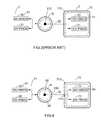
- FIG. 1shows a high-side transistor drive circuit.
- a floating circuit 10is applied to control the on/off state of a high-side transistor 11 .
- An NMOS transistor 12is connected to receive a control signal S 1 through an inverter 13 in a low-side circuit.
- the NMOS transistor 12comprises a drain region 120 coupled to an inverter 17 of the floating circuit 10 .
- the high-side transistor 11is coupled to a low-side transistor 14 at a common node where an output voltage V O is generated.
- a charge-pump capacitor 15provides a supply voltage to the floating circuit 10 .
- a voltage V Dcharges the charge-pump capacitor 15 through a diode 16 once the low-side transistor 14 is turned on according to a control signal S 2 .
- the ground reference of the charge-pump capacitor 15is pulled to the level of a voltage source V IN when the high-side transistor 11 is turned on.
- FIG. 2shows a top view of a conventional semiconductor device of the high-side inverter 17 and the low-side inverter 13 shown in FIG. 1 .
- the integrated circuitincludes a high-side region 2 to form high-side devices, such as the high-side inverter 17 .
- a barrier 170is disposed between the high-side region 2 and a low-side region 3 .
- the drain region 120 of the NMOS transistor 12is coupled to an NMOS transistor 20 and a PMOS transistor 21 of the high-side region 2 through a high-side conduction line 22 , and a gate region of the NMOS transistor 12 is coupled to an NMOS transistor 30 and a PMOS transistor 31 of the low-side region 3 .
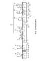
- FIG. 3shows a cross view of a conventional semiconductor structure of the semiconductor device shown in FIG. 2 .
- the NMOS transistor 12is disposed in an N-type well 102 .
- An N + conductivity type regionforms the drain region (D) 120
- another N + conductivity type regionforms a source region (S) 121
- a poly-silicon material between the drain region 120 and the source region 121forms a gate electrode (G) 122 .
- the gate electrode 122is disposed above oxides 123 for controlling the current flow in the conduction channel.
- the high-side devicescomprise the NMOS transistor 20 and the PMOS transistor 21 to serve as the high-side inverter 17 .
- an N + conductivity type regionis disposed in a P-type well 204 as a source region (S) 200 , another N + conductivity type region disposed in an N-type region 201 (N-type Double diffusion region, wherein the N + conductivity type region has a heavy diffusion concentration, and the N-type region 201 has a light diffusion concentration) forms a drain region (D) 202 , and a poly-silicon material between the drain region 202 and the source region 200 forms a gate electrode (G) 203 .
- a P + conductivity type regionis disposed in the N-type well 102 as a source region (S) 210 , another P + conductivity type region disposed in a P-type region 211 (P-type Double diffusion region, wherein the P + conductivity type region has a heavy diffusion concentration, and the P-type region 211 has a light diffusion concentration) forms a drain region (D) 212 , and a poly-silicon material between the drain region 212 and the source region 210 forms a gate electrode (G) 213 .
- the P-type well barrier 170is composed of a P + conductivity type region 171 .
- a P diffusion regions 172is disposed in the N-type well 102 .
- the high-side conduction line (500V) 22is coupled across the P-type well barrier 170 .
- the low-side devicescomprise the NMOS transistor 30 and the PMOS transistor 31 to serve as the low-side inverter 13 .
- the NMOS transistor 30 and the PMOS transistor 31are disposed in the deep N-type well 102 .
- the NMOS transistor 30comprises an N + conductivity type region as a drain region (D) 40 , and another N + conductivity type region disposed in a P-type well 41 as a source region (S) 42 .
- a poly-silicon material between the drain region 40 and the source region 42forms a gate electrode (G) 43 .
- the PMOS transistor 31comprises a P + conductivity type region as a source region (S) 50 , and another P + conductivity type region disposed in a P-type well 51 as a drain region (D) 52 .
- a poly-silicon material between the drain region 52 and the source region 50forms a gate electrode 53 .
- the drawback of the conventional semiconductor structureis that the operation voltage of the high-side conduction line is lower because dielectric breakdown voltage between high-side conduction line 22 and the metal of the barrier 170 (Metal-to-Metal dielectric breakdown voltage) is 500 V.
- the operation voltage of the NMOS transistor 20is 15V. Higher dielectric breakdown voltage and operation voltage is appreciated.
- An exemplary embodiment a method for forming a semiconductor devicecomprises steps: forming a substrate of a first conductivity type; forming a layer of a second conductivity type on the substrate; forming a deep well of the second conductivity type, wherein the deep well is extended down from a surface of the substrate; forming a well of the first conductivity type from the surface of the substrate, wherein the well is disposed within the deep well and on the layer; disposing a first poly-silicon material on the deep-well; and forming first and second regions of the second conductivity type within the well.
- FIG. 1shows a high-side transistor drive circuit
- FIG. 2shows a top view of a conventional semiconductor device of the high-side inverter and the low-side inverter shown in FIG. 1 ;
- FIG. 3shows a cross view of a conventional semiconductor structure of the semiconductor device shown in FIG. 2 ;
- FIG. 4is a top view of a semiconductor device for a high-side device and a low-side devices of an exemplary embodiment
- FIG. 5show a cross section view of the semiconductor device shown in FIG. 4 ;
- FIG. 6is flow chart of a method for forming the semiconductor device in the embodiment with FIG. 5 .
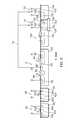
- a drain region 80 of an NMOS transistor 8is coupled to an NMOS transistor 73 and a PMOS transistor 72 of the high-side region 70 through the high-side conduction line 10 , and a gate region of the NMOS transistor 8 is coupled to an NMOS transistor 63 and a PMOS transistor 62 of the low-side region 71 .
- a source region 82 of the NMOS transistor 8has an opening 820 which is formed corresponding to the path of the high-side conduction line 10 .
- FIG. 5shows a cross section view of the semiconductor device shown in FIG. 4 .
- the NMOS transistor 8is disposed in an N-type well 102 .
- An N + conductivity type regionforms the drain region (D) 80
- another N + conductivity type regionforms the source region (S) 82
- a poly-silicon material disposed between the drain region 80 and the source region 82forms a gate electrode (G) 84 .
- the gate electrode 84is disposed above oxides 83 for controlling the current flow in the conduction channel.
- the high-side devices 60comprise the NMOS transistor 73 and the PMOS transistor 72 .
- an N + conductivity type layer 730is disposed on the P substrate P_SUB for insulation, which is define an insulation layer in the embodiment, and a P ⁇ conductivity type region is formed on the N + conductivity type layer 730 as a deep P-type well 731 .
- An N + conductivity type region disposed in the N + conductivity type layer 730forms a source region (S) 732 , another N + conductivity type region disposed in an N-type region 733 (N-type Double diffusion region, wherein the N + conductivity type region has a heavy diffusion concentration, and the N-type region 733 has a light diffusion concentration) forms a drain region (D) 734 , and a poly-silicon material disposed between the drain region 734 and the source region 732 forms a gate electrode 735 .
- a P + conductivity type regionis disposed in the N-type well 102 as a source region (S) 720 (third region), another P + conductivity type region disposed in a P-type region (fifth region) 721 (P-type Double diffusion region, wherein the P + conductivity type region has a heavy diffusion concentration, and the P-type region 721 has a light diffusion concentration) forms a drain region (D) (fourth region) 722 , and a poly-silicon material disposed between the drain region 722 and the source region 720 forms a gate electrode 723 .
- a P diffusion region 103forms the P-type well barrier 700 disposed in the N-type well 102 .
- the high-side conduction line 10which is disposed above the opening 820 and the open area 710 is coupled to the gate regions 723 and 735 of the PMOS transistor 72 and the NMOS transistor 73 .
- the low-side device 61comprises the NMOS transistor 63 and the PMOS transistor 62 to serve as a low-side inverter.
- the NMOS transistor 63 and the PMOS transistor 62are disposed in the deep N-type well 102 .
- the NMOS transistor 63comprises an N + conductivity type region as a drain region (D) 630 , and another N + conductivity type region disposed in a P-type well 631 as a source region (S) 632 .
- a poly-silicon material between the drain region 630 and the source region 632forms a gate electrode (G) 633 .
- the PMOS transistor 62comprises a P + conductivity type region as a source region (S) 620 , and another P + conductivity type region disposed in a P-type well 621 as a drain region (D) 622 .
- a poly-silicon material between the source region 620 and the drain region 622forms a gate electrode (G) 623 .
- the semiconductor device of the embodimenthas a deeper P-type well 731 for the NMOS transistor 73 , so the operation voltage of the high-side NMOS transistor 73 is increased, such as 30V in the embodiment.
- the opening 820 and the open area 710are formed under the high-side conduction line 10 , so that the operation voltage of the high-side conduction line 10 is increased to 700V due to higher metal-to-poly breakdown voltage.
- a substrate having a first conductive typesuch as a P-substrate P_SUB is formed (step 600 ).
- a layer having a second conductive type, such as N + conductivity type layer 730is formed on the P substrate P_SUB (step 610 ).
- the layer 730is formed within the P-substrate P_SUB.
- a deep well having a second conductive typesuch as N-type deep well 102 , is extended down from a surface of the P-substrate P_SUB (step 620 ).
- the P + conductivity type regions 722 , 720 , 620 and 622are formed within the P-type well 721 , N-type deep well 102 , N-type deep well 102 , and P-type region 621 , respectively (step 680 ).
- Subsequent processes, such as connecting a high-side conduction line 10 between the drain region (D) 80 and the NMOS transistor 73 and PMOS transistor 72 , and other processes,are preformed to finish the semiconductor manufacture (step 690 ).
- the N + conductivity type source region 732 , the N + conductivity type drain region 734 , and the gate electrode 735form a high-side device, such as the NMOS transistor 73 in FIG. 4 .
- the P + conductivity type source region 720 , the P + conductivity type drain region 722 , and the gate electrode 723form another high-side device, such as the PMOS transistor 72 in FIG. 4 .
Landscapes
- Metal-Oxide And Bipolar Metal-Oxide Semiconductor Integrated Circuits (AREA)
Abstract
Description
- The present application claims the benefit of U.S. provisional application entitled “SEMICONDUCTOR STRUCTURE FOR HIGH-SIDE DEVIDES INTEGRATED WITH LOW SIDE DEVICEW”, Ser. No. 61/210,114, filed Mar. 12, 2009.
- 1. Field of the Invention
- The invention relates to a semiconductor device, and more particularly to a new high-side device integrated with an original low-side device.
- 2. Description of the Related Art
- A variety of power suppliers and motor drivers utilize bridge circuits to control a power source to a load. The bridge circuit normally has a high-side transistor connected to the power source and a low-side transistor connected to the ground. A common node between the high-side transistor and the low-side transistor is coupled to the load. As the transistors are controlled to alternately conduct, the voltage of the common node swings between voltage levels of the power source and the ground. Therefore, a high-side transistor driver requires a charge pump circuit and/or a floating drive circuit in order to fully turn on the high-side transistor. In recent development, many floating circuits are being disclosed in U.S. Pat. No. 6,344,959 (Milazzo), U.S. Pat. No. 6,781,422 (Yang) and U.S. Pat. No. 6,836,173 (Yang).
FIG. 1 shows a high-side transistor drive circuit. Afloating circuit 10 is applied to control the on/off state of a high-side transistor 11. AnNMOS transistor 12 is connected to receive a control signal S1through aninverter 13 in a low-side circuit. TheNMOS transistor 12 comprises adrain region 120 coupled to aninverter 17 of thefloating circuit 10. The high-side transistor 11 is coupled to a low-side transistor 14 at a common node where an output voltage VOis generated. A charge-pump capacitor 15 provides a supply voltage to thefloating circuit 10. A voltage VDcharges the charge-pump capacitor 15 through adiode 16 once the low-side transistor 14 is turned on according to a control signal S2. The ground reference of the charge-pump capacitor 15 is pulled to the level of a voltage source VINwhen the high-side transistor 11 is turned on.FIG. 2 shows a top view of a conventional semiconductor device of the high-side inverter 17 and the low-side inverter 13 shown inFIG. 1 . The integrated circuit includes a high-side region 2 to form high-side devices, such as the high-side inverter 17. Abarrier 170 is disposed between the high-side region 2 and a low-side region 3.- The
drain region 120 of theNMOS transistor 12 is coupled to anNMOS transistor 20 and aPMOS transistor 21 of the high-side region 2 through a high-side conduction line 22, and a gate region of theNMOS transistor 12 is coupled to anNMOS transistor 30 and aPMOS transistor 31 of the low-side region 3. FIG. 3 shows a cross view of a conventional semiconductor structure of the semiconductor device shown inFIG. 2 . TheNMOS transistor 12 is disposed in an N-type well 102. An N+ conductivity type region forms the drain region (D)120, another N+ conductivity type region forms a source region (S)121, and a poly-silicon material between thedrain region 120 and thesource region 121 forms a gate electrode (G)122. Wherein thegate electrode 122 is disposed aboveoxides 123 for controlling the current flow in the conduction channel. The high-side devices comprise theNMOS transistor 20 and thePMOS transistor 21 to serve as the high-side inverter 17. In theNMOS transistor 20, an N+ conductivity type region is disposed in a P-type well 204 as a source region (S)200, another N+ conductivity type region disposed in an N-type region201 (N-type Double diffusion region, wherein the N+ conductivity type region has a heavy diffusion concentration, and the N-type region 201 has a light diffusion concentration) forms a drain region (D)202, and a poly-silicon material between thedrain region 202 and thesource region 200 forms a gate electrode (G)203. For thePMOS transistor 21, a P+ conductivity type region is disposed in the N-type well 102 as a source region (S)210, another P+ conductivity type region disposed in a P-type region211 (P-type Double diffusion region, wherein the P+ conductivity type region has a heavy diffusion concentration, and the P-type region 211 has a light diffusion concentration) forms a drain region (D)212, and a poly-silicon material between thedrain region 212 and thesource region 210 forms a gate electrode (G)213. The P-type well barrier 170 is composed of a P+conductivity type region 171.A P diffusion regions 172 is disposed in the N-type well 102. The high-side conduction line (500V)22 is coupled across the P-type well barrier 170.- The low-side devices comprise the
NMOS transistor 30 and thePMOS transistor 31 to serve as the low-side inverter 13. TheNMOS transistor 30 and thePMOS transistor 31 are disposed in the deep N-type well 102. TheNMOS transistor 30 comprises an N+ conductivity type region as a drain region (D)40, and another N+ conductivity type region disposed in a P-type well 41 as a source region (S)42. A poly-silicon material between thedrain region 40 and thesource region 42 forms a gate electrode (G)43. ThePMOS transistor 31 comprises a P+ conductivity type region as a source region (S)50, and another P+ conductivity type region disposed in a P-type well 51 as a drain region (D)52. A poly-silicon material between thedrain region 52 and thesource region 50 forms agate electrode 53. - The drawback of the conventional semiconductor structure is that the operation voltage of the high-side conduction line is lower because dielectric breakdown voltage between high-
side conduction line 22 and the metal of the barrier170 (Metal-to-Metal dielectric breakdown voltage) is 500 V. The operation voltage of theNMOS transistor 20 is 15V. Higher dielectric breakdown voltage and operation voltage is appreciated. - An exemplary embodiment of a semiconductor device comprises a substrate of a first conductivity type, a deep well of a second conductivity type, and a first high-side device. The deep well of a second conductivity type is formed on the substrate. The first high-side device is disposed within the deep well and comprises an insulation layer of the second conductivity type, a well of the first conductivity type, first and second regions of the second conductivity type, and a first poly-silicon material. The insulation layer of the second conductivity type is formed on the substrate. The well of the first conductivity type is formed within the deep well. The first and second regions of the second conductivity type are formed within the well. The first poly-silicon material is disposed between the first region and the second region and on the deep well.
- An exemplary embodiment a method for forming a semiconductor device comprises steps: forming a substrate of a first conductivity type; forming a layer of a second conductivity type on the substrate; forming a deep well of the second conductivity type, wherein the deep well is extended down from a surface of the substrate; forming a well of the first conductivity type from the surface of the substrate, wherein the well is disposed within the deep well and on the layer; disposing a first poly-silicon material on the deep-well; and forming first and second regions of the second conductivity type within the well.
- A detailed description is given in the following embodiments with reference to the accompanying drawings.
- The invention can be more fully understood by reading the subsequent detailed description and examples with references made to the accompanying drawings, wherein:
FIG. 1 shows a high-side transistor drive circuit;FIG. 2 shows a top view of a conventional semiconductor device of the high-side inverter and the low-side inverter shown inFIG. 1 ;FIG. 3 shows a cross view of a conventional semiconductor structure of the semiconductor device shown inFIG. 2 ;FIG. 4 is a top view of a semiconductor device for a high-side device and a low-side devices of an exemplary embodiment;FIG. 5 show a cross section view of the semiconductor device shown inFIG. 4 ; andFIG. 6 is flow chart of a method for forming the semiconductor device in the embodiment withFIG. 5 .- The following description is of the best-contemplated mode of carrying out the invention. This description is made for the purpose of illustrating the general principles of the invention and should not be taken in a limiting sense. The scope of the invention is best determined by reference to the appended claims.
FIG. 4 is a top view of a semiconductor device for a high-side device (inverter)60 and a low-side device (inverter)61 of an exemplary embodiment.FIG. 5 shows a cross-section view of the semiconductor device according to an exemplary embodiment. Referring toFIG. 4 , the semiconductor device comprises a high-side region 70 to form the high-side device, such as a high-side inverter 60 in the embodiment. Abarrier 700 is disposed between the high-side region 70 and a low-side region 71. Thebarrier 700 has anopen area 710 which is formed under a high-side conduction line 10.- A
drain region 80 of anNMOS transistor 8 is coupled to anNMOS transistor 73 and aPMOS transistor 72 of the high-side region 70 through the high-side conduction line 10, and a gate region of theNMOS transistor 8 is coupled to anNMOS transistor 63 and aPMOS transistor 62 of the low-side region 71. Asource region 82 of theNMOS transistor 8 has anopening 820 which is formed corresponding to the path of the high-side conduction line 10. FIG. 5 shows a cross section view of the semiconductor device shown inFIG. 4 . TheNMOS transistor 8 is disposed in an N-type well 102. An N+ conductivity type region forms the drain region (D)80, another N+ conductivity type region forms the source region (S)82, and a poly-silicon material disposed between thedrain region 80 and thesource region 82 forms a gate electrode (G)84. Wherein thegate electrode 84 is disposed aboveoxides 83 for controlling the current flow in the conduction channel.- The high-
side devices 60 comprise theNMOS transistor 73 and thePMOS transistor 72. In theNMOS transistor 73, an N+conductivity type layer 730 is disposed on the P substrate P_SUB for insulation, which is define an insulation layer in the embodiment, and a P− conductivity type region is formed on the N+conductivity type layer 730 as a deep P-type well 731. An N+ conductivity type region disposed in the N+conductivity type layer 730 forms a source region (S)732, another N+ conductivity type region disposed in an N-type region733 (N-type Double diffusion region, wherein the N+ conductivity type region has a heavy diffusion concentration, and the N-type region 733 has a light diffusion concentration) forms a drain region (D)734, and a poly-silicon material disposed between thedrain region 734 and thesource region 732 forms agate electrode 735. For thePMOS transistor 72, a P+ conductivity type region is disposed in the N-type well102 as a source region (S)720 (third region), another P+ conductivity type region disposed in a P-type region (fifth region)721 (P-type Double diffusion region, wherein the P+ conductivity type region has a heavy diffusion concentration, and the P-type region 721 has a light diffusion concentration) forms a drain region (D) (fourth region)722, and a poly-silicon material disposed between thedrain region 722 and thesource region 720 forms agate electrode 723. As shown inFIG. 4 , aP diffusion region 103 forms the P-type well barrier 700 disposed in the N-type well 102. The high-side conduction line 10 which is disposed above theopening 820 and theopen area 710 is coupled to thegate regions PMOS transistor 72 and theNMOS transistor 73. - The low-
side device 61 comprises theNMOS transistor 63 and thePMOS transistor 62 to serve as a low-side inverter. TheNMOS transistor 63 and thePMOS transistor 62 are disposed in the deep N-type well 102. TheNMOS transistor 63 comprises an N+ conductivity type region as a drain region (D)630, and another N+ conductivity type region disposed in a P-type well631 as a source region (S)632. A poly-silicon material between thedrain region 630 and thesource region 632 forms a gate electrode (G)633. ThePMOS transistor 62 comprises a P+ conductivity type region as a source region (S)620, and another P+ conductivity type region disposed in a P-type well621 as a drain region (D)622. A poly-silicon material between thesource region 620 and thedrain region 622 forms a gate electrode (G)623. - According to the aforementioned description, the semiconductor device of the embodiment has a deeper P-type well731 for the
NMOS transistor 73, so the operation voltage of the high-side NMOS transistor 73 is increased, such as 30V in the embodiment. Besides, theopening 820 and theopen area 710 are formed under the high-side conduction line 10, so that the operation voltage of the high-side conduction line 10 is increased to 700V due to higher metal-to-poly breakdown voltage. - The following will describe the flow of a method for forming the semiconductor device in the embodiment with
FIG. 5 . Referring toFIG. 6 , first, a substrate having a first conductive type, such as a P-substrate P_SUB is formed (step600). A layer having a second conductive type, such as N+conductivity type layer 730 is formed on the P substrate P_SUB (step610). Thelayer 730 is formed within the P-substrate P_SUB. Then, a deep well having a second conductive type, such as N-type deep well102, is extended down from a surface of the P-substrate P_SUB (step620). A deep well having a first conductive type, such as P-type well 731, is then formed from a surface of the P-substrate P_SUB (step630). Wherein the P-type well 731 is disposed within the N-type deep well102 and on the N+conductivity type layer 730. Thus, the N+conductivity type layer 730 provides isolation between the P substrate P_SUB and the P-type well 731. Next, instep 640, a plurality of first doping regions (such as P-type regions deep well 102. Then, a second doping region (such as an N-type region733) is formed in the P-type well731 (step650). Next,field oxides 83 is formed on the N-type deep well102, and thegate regions conductivity type regions type well 731, N-type region 733, N-type deep well102, and P-type region 631, respectively (step670). Next, the P+conductivity type regions type well 721, N-type deep well102, N-type deep well102, and P-type region 621, respectively (step680). Subsequent processes, such as connecting a high-side conduction line 10 between the drain region (D)80 and theNMOS transistor 73 andPMOS transistor 72, and other processes, are preformed to finish the semiconductor manufacture (step690). - In the embodiment, the N+ conductivity
type source region 732, the N+ conductivitytype drain region 734, and thegate electrode 735 form a high-side device, such as theNMOS transistor 73 inFIG. 4 . The P+ conductivitytype source region 720, the P+ conductivitytype drain region 722, and thegate electrode 723 form another high-side device, such as thePMOS transistor 72 inFIG. 4 . - While the invention has been described by way of example and in terms of the preferred embodiments, it is to be understood that the invention is not limited to the disclosed embodiments. To the contrary, it is intended to cover various modifications and similar arrangements (as would be apparent to those skilled in the art). Therefore, the scope of the appended claims should be accorded the broadest interpretation so as to encompass all such modifications and similar arrangements.
Claims (14)
Priority Applications (1)
| Application Number | Priority Date | Filing Date | Title |
|---|---|---|---|
| US12/574,793US9184097B2 (en) | 2009-03-12 | 2009-10-07 | Semiconductor devices and formation methods thereof |
Applications Claiming Priority (2)
| Application Number | Priority Date | Filing Date | Title |
|---|---|---|---|
| US21011409P | 2009-03-12 | 2009-03-12 | |
| US12/574,793US9184097B2 (en) | 2009-03-12 | 2009-10-07 | Semiconductor devices and formation methods thereof |
Publications (2)
| Publication Number | Publication Date |
|---|---|
| US20100230749A1true US20100230749A1 (en) | 2010-09-16 |
| US9184097B2 US9184097B2 (en) | 2015-11-10 |
Family
ID=42729977
Family Applications (1)
| Application Number | Title | Priority Date | Filing Date |
|---|---|---|---|
| US12/574,793Active2031-06-30US9184097B2 (en) | 2009-03-12 | 2009-10-07 | Semiconductor devices and formation methods thereof |
Country Status (3)
| Country | Link |
|---|---|
| US (1) | US9184097B2 (en) |
| CN (1) | CN101853856B (en) |
| TW (1) | TWI404193B (en) |
Cited By (2)
| Publication number | Priority date | Publication date | Assignee | Title |
|---|---|---|---|---|
| US20150311280A1 (en)* | 2012-11-28 | 2015-10-29 | Shenzhen Sunmoon Microelectronics Co., Ltd. | A high voltage device with composite structure and a starting circuit |
| TWI605498B (en)* | 2016-09-28 | 2017-11-11 | 台灣積體電路製造股份有限公司 | Semiconductor device and method of manufacturing same |
Families Citing this family (2)
| Publication number | Priority date | Publication date | Assignee | Title |
|---|---|---|---|---|
| US9633734B1 (en)* | 2016-07-14 | 2017-04-25 | Ememory Technology Inc. | Driving circuit for non-volatile memory |
| US10580890B2 (en) | 2017-12-04 | 2020-03-03 | Texas Instruments Incorporated | Drain extended NMOS transistor |
Citations (105)
| Publication number | Priority date | Publication date | Assignee | Title |
|---|---|---|---|---|
| US4300150A (en)* | 1980-06-16 | 1981-11-10 | North American Philips Corporation | Lateral double-diffused MOS transistor device |
| US4403395A (en)* | 1979-02-15 | 1983-09-13 | Texas Instruments Incorporated | Monolithic integration of logic, control and high voltage interface circuitry |
| US4927776A (en)* | 1985-10-17 | 1990-05-22 | Nec Corporation | Method of producing semiconductor integrated circuit device including bipolar transistor and insulated gate field effect transistor |
| US5012322A (en)* | 1987-05-18 | 1991-04-30 | Allegro Microsystems, Inc. | Semiconductor die and mounting assembly |
| US5021860A (en)* | 1987-10-15 | 1991-06-04 | Sgs-Thomson Microelectronics S.R.L. | Integrated device for shielding the injection of charges into the substrate |
| US5065213A (en)* | 1987-12-22 | 1991-11-12 | Sgs-Thomson Microelectronics S.R.L. | Integrated high-voltage bipolar power transistor and low voltage mos power transistor structure in the emitter switching configuration and relative manufacturing process |
| US5163178A (en)* | 1989-12-28 | 1992-11-10 | Sony Corporation | Semiconductor device having enhanced impurity concentration profile |
| US5204541A (en)* | 1991-06-28 | 1993-04-20 | Texas Instruments Incorporated | Gated thyristor and process for its simultaneous fabrication with high- and low-voltage semiconductor devices |
| US5319234A (en)* | 1992-02-17 | 1994-06-07 | Mitsubishi Denki Kabushiki Kaisha | C-BiCMOS semiconductor device |
| US5422508A (en)* | 1992-09-21 | 1995-06-06 | Siliconix Incorporated | BiCDMOS structure |
| US5471085A (en)* | 1993-10-04 | 1995-11-28 | Mitsubishi Denki Kabushiki Kaisha | Semiconductor device with polycrystalline silicon emitter conductive layer |
| US5495124A (en)* | 1993-01-08 | 1996-02-27 | Mitsubishi Denki Kabushiki Kaisha | Semiconductor device with increased breakdown voltage |
| US5501994A (en)* | 1994-04-08 | 1996-03-26 | Texas Instruments Incorporated | Extended drain resurf lateral DMOS devices |
| US5504368A (en)* | 1991-09-24 | 1996-04-02 | Matsushita Electric Industrial Co., Ltd. | Semiconductor integrated circuit device with self-aligned superhigh speed bipolar transistor |
| US5517046A (en)* | 1993-11-19 | 1996-05-14 | Micrel, Incorporated | High voltage lateral DMOS device with enhanced drift region |
| US5591657A (en)* | 1993-10-26 | 1997-01-07 | Fuji Electric Co., Ltd. | Semiconductor apparatus manufacturing method employing gate side wall self-aligning for masking |
| US5631487A (en)* | 1993-07-30 | 1997-05-20 | Nec Corporation | Semiconductor device and motor driver circuit using the same |
| US5637889A (en)* | 1995-02-28 | 1997-06-10 | Sgs-Thomson Microelectronics, Inc. | Composite power transistor structures using semiconductor materials with different bandgaps |
| US5643809A (en)* | 1995-03-08 | 1997-07-01 | Integrated Device Technology, Inc. | Method for making high speed poly-emitter bipolar transistor |
| US5648281A (en)* | 1992-09-21 | 1997-07-15 | Siliconix Incorporated | Method for forming an isolation structure and a bipolar transistor on a semiconductor substrate |
| US5852314A (en)* | 1995-05-02 | 1998-12-22 | SGS--Thomson Microelectronics S.r.l. | Thin epitaxy resurf integrated circuit containing high voltage p-channel and n-channel devices with source or drain not tied to ground |
| US5907171A (en)* | 1995-05-18 | 1999-05-25 | Texas Instruments Incorporated | Method of making floating-gate memory-cell array with digital logic transistors |
| US5943564A (en)* | 1996-02-13 | 1999-08-24 | National Semiconductor Corporation | BiCMOS process for forming double-poly MOS and bipolar transistors with substantially identical device architectures |
| US5953600A (en)* | 1996-11-19 | 1999-09-14 | Sgs-Thomson Microelectronics S.A | Fabrication of bipolar/CMOS integrated circuits |
| US6137153A (en)* | 1998-02-13 | 2000-10-24 | Advanced Micro Devices, Inc. | Floating gate capacitor for use in voltage regulators |
| US6194764B1 (en)* | 1997-09-30 | 2001-02-27 | Infineon Technologies Ag | Integrated semiconductor circuit with protection structure for protecting against electrostatic discharge |
| US6238959B1 (en)* | 1999-08-03 | 2001-05-29 | United Microelectronics Corp. | Method of fabricating LDMOS transistor |
| US6245609B1 (en)* | 1999-09-27 | 2001-06-12 | Taiwan Semiconductor Manufacturing Company | High voltage transistor using P+ buried layer |
| US6255713B1 (en)* | 1999-07-27 | 2001-07-03 | Taiwan Semiconductor Manufacturing Corporation | Current source using merged vertical bipolar transistor based on gate induced gate leakage current |
| US20010013610A1 (en)* | 1999-08-02 | 2001-08-16 | Min-Hwa Chi | Vertical bipolar transistor based on gate induced drain leakage current |
| US6281565B1 (en)* | 1997-12-25 | 2001-08-28 | Sony Corporation | Semiconductor device and method for producing the same |
| US6303419B1 (en)* | 2000-03-24 | 2001-10-16 | Industrial Technology Research Institute | Method for fabricating a BiCMOS device featuring twin wells and an N type epitaxial layer |
| US6303961B1 (en)* | 1998-04-29 | 2001-10-16 | Aqere Systems Guardian Corp. | Complementary semiconductor devices |
| US20020030238A1 (en)* | 2000-09-11 | 2002-03-14 | Kabushiki Kaisha Toshiba | Semiconductor device |
| US6376891B1 (en)* | 1995-12-30 | 2002-04-23 | Mitsubishi Denki Kabushiki Kaisha | High voltage breakdown isolation semiconductor device and manufacturing process for making the device |
| US20020053710A1 (en)* | 1999-04-16 | 2002-05-09 | Eiji Io | Semiconductor device having a high breakdown voltage |
| US20020079514A1 (en)* | 2000-12-27 | 2002-06-27 | Hower Philip L. | Metal-oxide-semiconductor transistor structure and method of manufacturing same |
| US20020106860A1 (en)* | 2000-04-13 | 2002-08-08 | Sanyo Electric Co., Ltd., A Japan Corporation | Semiconductor device and method of manufacturing the same |
| US20020109202A1 (en)* | 2001-02-13 | 2002-08-15 | Te-Wei Chen | Diode structure on MOS wafer |
| US6440812B2 (en)* | 1995-08-25 | 2002-08-27 | Micron Technology, Inc. | Angled implant to improve high current operation of bipolar transistors |
| US20020182805A1 (en)* | 2001-05-02 | 2002-12-05 | Ching-Hsiang Hsu | Structure of a low-voltage channel write/erase flash memory cell and fabricating method thereof |
| US20020179977A1 (en)* | 2000-05-30 | 2002-12-05 | Ting-Wah Wong | Integrated radio frequency circuits |
| US20020190308A1 (en)* | 2001-05-29 | 2002-12-19 | Ching-Hsiang Hsu | Structure of an embedded channel write/erase flash memory cell and fabricating method thereof |
| US6569742B1 (en)* | 1998-12-25 | 2003-05-27 | Hitachi, Ltd. | Method of manufacturing semiconductor integrated circuit device having silicide layers |
| US20030173624A1 (en)* | 2002-02-23 | 2003-09-18 | Fairchild Korea Semiconductor Ltd. | High breakdown voltage low on-resistance lateral DMOS transistor |
| US6729886B2 (en)* | 2002-06-11 | 2004-05-04 | Texas Instruments Incorporated | Method of fabricating a drain isolated LDMOS device |
| US6750489B1 (en)* | 2002-10-25 | 2004-06-15 | Foveon, Inc. | Isolated high voltage PMOS transistor |
| US20040152288A1 (en)* | 2002-12-31 | 2004-08-05 | Trogolo Joe R. | Transistors formed with grid or island implantation masks to form reduced diffusion-depth regions without additional masks and process steps |
| US6815794B2 (en)* | 2002-03-05 | 2004-11-09 | Samsung Electronics Co., Ltd. | Semiconductor devices with multiple isolation structure and methods for fabricating the same |
| US20040251492A1 (en)* | 2003-06-13 | 2004-12-16 | John Lin | LDMOS transistors and methods for making the same |
| US20050006701A1 (en)* | 2003-07-07 | 2005-01-13 | Tzu-Chiang Sung | High voltage metal-oxide semiconductor device |
| US6844578B2 (en)* | 2001-03-28 | 2005-01-18 | Seiko Instruments Inc. | Semiconductor integrated circuit device and manufacturing method therefor |
| US6879003B1 (en)* | 2004-06-18 | 2005-04-12 | United Microelectronics Corp. | Electrostatic discharge (ESD) protection MOS device and ESD circuitry thereof |
| US6878996B2 (en)* | 2002-05-29 | 2005-04-12 | Infineon Technologies Ag | MOS power transistor |
| US20050082565A1 (en)* | 2003-10-17 | 2005-04-21 | Stmicroelectronics S.A. | Isolated HF-control SCR switch |
| US20050106825A1 (en)* | 2003-11-13 | 2005-05-19 | Budong You | Method of fabricating a lateral double-diffused mosfet (LDMOS) transistor and a conventional CMOS transistor |
| US20050179092A1 (en)* | 2003-12-30 | 2005-08-18 | Dongbuanam Semiconductor Inc. | Method of fabricating high voltage device using double epitaxial growth |
| US6949424B2 (en)* | 2003-08-28 | 2005-09-27 | Texas Instruments Incorporated | Single poly-emitter PNP using DWELL diffusion in a BiCMOS technology |
| US20050221551A1 (en)* | 2002-04-26 | 2005-10-06 | Naohiro Ueda | Method of forming semiconductor integrated device |
| US20060006462A1 (en)* | 2004-07-12 | 2006-01-12 | Chi-Hsuen Chang | Method and apparatus for a semiconductor device having low and high voltage transistors |
| US20060065947A1 (en)* | 2002-12-20 | 2006-03-30 | Exar Corporation | Reverse-biased p/n wells isolating a cmos inductor from the substrate |
| US7049663B2 (en)* | 2004-03-22 | 2006-05-23 | Sunplus Technology Co,Ltd. | ESD protection device with high voltage and negative voltage tolerance |
| US20060113592A1 (en)* | 2004-05-03 | 2006-06-01 | Sameer Pendharkar | Robust DEMOS transistors and method for making the same |
| US20060124999A1 (en)* | 2004-12-15 | 2006-06-15 | Texas Instruments Incorporated | Drain extended PMOS transistors and methods for making the same |
| US7091079B2 (en)* | 2004-11-11 | 2006-08-15 | United Microelectronics Corp. | Method of forming devices having three different operation voltages |
| US20060255850A1 (en)* | 2004-09-03 | 2006-11-16 | International Business Machines Corporation | High speed latch circuits using gated diodes |
| US7161198B2 (en)* | 2001-09-12 | 2007-01-09 | Seiko Instruments Inc. | Semiconductor integrated circuit device having MOS transistor |
| US7195965B2 (en)* | 2002-10-25 | 2007-03-27 | Texas Instruments Incorporated | Premature breakdown in submicron device geometries |
| US20070132033A1 (en)* | 2005-12-12 | 2007-06-14 | Taiwan Semiconductor Manufacturing Company, Ltd. | High voltage CMOS devices |
| US20070181909A1 (en)* | 2006-02-03 | 2007-08-09 | Semiconductor Components Industries, Llc. | Schottky diode structure with enhanced breakdown voltage and method of manufacture |
| US20070249135A1 (en)* | 2006-04-19 | 2007-10-25 | Texas Instruments Incorporated | Collector tailored structures for integration of binary junction transistors |
| US20070252731A1 (en)* | 2006-04-26 | 2007-11-01 | Magnachip Semiconductor, Ltd. | Semiconductor integrated circuit |
| US20070275509A1 (en)* | 2003-08-06 | 2007-11-29 | Samsung Electronics Co., Ltd. | Method of manufacturing NOR-type mask ROM device and semiconductor device including the same |
| US7304387B2 (en)* | 2005-06-08 | 2007-12-04 | Samsung Elecronics Co., Ltd. | Semiconductor integrated circuit device |
| US7329570B2 (en)* | 2004-12-29 | 2008-02-12 | Dongbu Electronics Co., Ltd. | Method for manufacturing a semiconductor device |
| US20080036027A1 (en)* | 2006-08-11 | 2008-02-14 | System General Corp. | Integrated circuit for a high-side transistor driver |
| US20080061867A1 (en)* | 2006-08-10 | 2008-03-13 | Cetin Kaya | Methods and apparatus to reduce substrate voltage bounces and spike voltages in switching amplifiers |
| US20080128756A1 (en)* | 2005-06-10 | 2008-06-05 | Fujitsu Limited | Semiconductor device, semiconductor system and semiconductor device manufacturing method |
| US20080138946A1 (en)* | 2004-07-15 | 2008-06-12 | Samsung Electronics Co., Ltd. | High frequency mos transistor, method of forming the same, and method of manufacturing a semiconductor device including the same |
| US7394133B1 (en)* | 2005-08-31 | 2008-07-01 | National Semiconductor Corporation | Dual direction ESD clamp based on snapback NMOS cell with embedded SCR |
| US20080173949A1 (en)* | 2007-01-19 | 2008-07-24 | Episil Technologies Inc. | Complementary metal-oxide-semiconductor field effect transistor |
| US20080237703A1 (en)* | 2007-03-28 | 2008-10-02 | Taiwan Semiconductor Manufacturing Co., Ltd. | High voltage semiconductor devices and methods for fabricating the same |
| US20080237777A1 (en)* | 2007-03-27 | 2008-10-02 | Alpha & Omega Semiconductor, Ltd | Completely decoupled high voltage and low voltage transistor manufacurting processes |
| US20080277728A1 (en)* | 2007-05-11 | 2008-11-13 | System General Corp. | Semiconductor structure for protecting an internal integrated circuit and method for manufacturing the same |
| US20080293202A1 (en)* | 2003-06-13 | 2008-11-27 | Denso Corporation | Method for manufacturing semiconductor device |
| US20090001461A1 (en)* | 2007-06-26 | 2009-01-01 | Choul-Joo Ko | Lateral dmos device and method for fabricating the same |
| US20090014791A1 (en)* | 2007-07-11 | 2009-01-15 | Great Wall Semiconductor Corporation | Lateral Power MOSFET With Integrated Schottky Diode |
| US7489007B2 (en)* | 2006-05-31 | 2009-02-10 | Advanced Analogic Technologies, Inc. | High-voltage lateral DMOS device |
| US7528032B2 (en)* | 2001-06-21 | 2009-05-05 | Seiko Instruments Inc. | Method for manufacturing semiconductor device |
| US20090152668A1 (en)* | 2007-12-14 | 2009-06-18 | Denso Dorporation | Semiconductor apparatus |
| US20090166721A1 (en)* | 2007-12-31 | 2009-07-02 | Marie Denison | Quasi-vertical gated npn-pnp esd protection device |
| US20090212373A1 (en)* | 2008-02-27 | 2009-08-27 | Fuji Electric Device Technology Co., Ltd. | Semiconductor device |
| US20090236679A1 (en)* | 2008-03-24 | 2009-09-24 | Puo-Yu Chiang | Schottky Diode Structures Having Deep Wells for Improving Breakdown Voltages |
| US7608895B2 (en)* | 2002-09-29 | 2009-10-27 | Advanced Analogic Technologies, Inc. | Modular CMOS analog integrated circuit and power technology |
| US7635621B2 (en)* | 2002-11-22 | 2009-12-22 | Micrel, Inc. | Lateral double-diffused metal oxide semiconductor (LDMOS) device with an enhanced drift region that has an improved Ron area product |
| US20100027172A1 (en)* | 2008-07-15 | 2010-02-04 | Semiconductor Manufacturing International (Shanghai) Corporation | Integrated electrostatic discharge (esd) device |
| US20100032756A1 (en)* | 2008-08-07 | 2010-02-11 | Texas Instruments Incorporated | Buried floating layer structure for improved breakdown |
| US7704819B2 (en)* | 2005-07-06 | 2010-04-27 | Hewlett-Packard Development Company, L.P. | Creating high voltage FETs with low voltage process |
| US7714390B2 (en)* | 2005-04-01 | 2010-05-11 | Stmicroelectronics S.A. | Integrated circuit comprising a substrate and a resistor |
| US20100148250A1 (en)* | 2008-12-11 | 2010-06-17 | United Microelectronics Corp. | Metal oxide semiconductor device |
| US20100151648A1 (en)* | 2007-08-29 | 2010-06-17 | Taiwan Semiconductor Manufacturing Company,Ltd. | Strained Channel Transistor |
| US20100213987A1 (en)* | 2009-02-20 | 2010-08-26 | Keita Takahashi | Semiconductor memory device and driving method for the same |
| US7843002B2 (en)* | 2007-07-03 | 2010-11-30 | Taiwan Semiconductor Manufacturing Company, Ltd. | Fully isolated high-voltage MOS device |
| US7906808B2 (en)* | 2008-07-09 | 2011-03-15 | Kabushiki Kaisha Toshiba | Semiconductor device |
| US20110254097A1 (en)* | 2004-10-29 | 2011-10-20 | Mitsuhiro Noguchi | Nonvolatile semiconductor memory device with twin-well |
Family Cites Families (1)
| Publication number | Priority date | Publication date | Assignee | Title |
|---|---|---|---|---|
| TWI397180B (en)* | 2008-12-17 | 2013-05-21 | Vanguard Int Semiconduct Corp | Horizontally diffused metal oxide semiconductor (LDMOS) device with electrostatic discharge protection capability in integrated circuits |
- 2009
- 2009-10-07USUS12/574,793patent/US9184097B2/enactiveActive
- 2009-12-25TWTW098144916Apatent/TWI404193B/enactive
- 2010
- 2010-01-20CNCN2010100007873Apatent/CN101853856B/ennot_activeExpired - Fee Related
Patent Citations (117)
| Publication number | Priority date | Publication date | Assignee | Title |
|---|---|---|---|---|
| US4403395A (en)* | 1979-02-15 | 1983-09-13 | Texas Instruments Incorporated | Monolithic integration of logic, control and high voltage interface circuitry |
| US4300150A (en)* | 1980-06-16 | 1981-11-10 | North American Philips Corporation | Lateral double-diffused MOS transistor device |
| US4927776A (en)* | 1985-10-17 | 1990-05-22 | Nec Corporation | Method of producing semiconductor integrated circuit device including bipolar transistor and insulated gate field effect transistor |
| US5012322A (en)* | 1987-05-18 | 1991-04-30 | Allegro Microsystems, Inc. | Semiconductor die and mounting assembly |
| US5021860A (en)* | 1987-10-15 | 1991-06-04 | Sgs-Thomson Microelectronics S.R.L. | Integrated device for shielding the injection of charges into the substrate |
| US5065213A (en)* | 1987-12-22 | 1991-11-12 | Sgs-Thomson Microelectronics S.R.L. | Integrated high-voltage bipolar power transistor and low voltage mos power transistor structure in the emitter switching configuration and relative manufacturing process |
| US5163178A (en)* | 1989-12-28 | 1992-11-10 | Sony Corporation | Semiconductor device having enhanced impurity concentration profile |
| US5204541A (en)* | 1991-06-28 | 1993-04-20 | Texas Instruments Incorporated | Gated thyristor and process for its simultaneous fabrication with high- and low-voltage semiconductor devices |
| US5504368A (en)* | 1991-09-24 | 1996-04-02 | Matsushita Electric Industrial Co., Ltd. | Semiconductor integrated circuit device with self-aligned superhigh speed bipolar transistor |
| US5319234A (en)* | 1992-02-17 | 1994-06-07 | Mitsubishi Denki Kabushiki Kaisha | C-BiCMOS semiconductor device |
| US5422508A (en)* | 1992-09-21 | 1995-06-06 | Siliconix Incorporated | BiCDMOS structure |
| US5648281A (en)* | 1992-09-21 | 1997-07-15 | Siliconix Incorporated | Method for forming an isolation structure and a bipolar transistor on a semiconductor substrate |
| US5495124A (en)* | 1993-01-08 | 1996-02-27 | Mitsubishi Denki Kabushiki Kaisha | Semiconductor device with increased breakdown voltage |
| US5631487A (en)* | 1993-07-30 | 1997-05-20 | Nec Corporation | Semiconductor device and motor driver circuit using the same |
| US5471085A (en)* | 1993-10-04 | 1995-11-28 | Mitsubishi Denki Kabushiki Kaisha | Semiconductor device with polycrystalline silicon emitter conductive layer |
| US5591657A (en)* | 1993-10-26 | 1997-01-07 | Fuji Electric Co., Ltd. | Semiconductor apparatus manufacturing method employing gate side wall self-aligning for masking |
| US5517046A (en)* | 1993-11-19 | 1996-05-14 | Micrel, Incorporated | High voltage lateral DMOS device with enhanced drift region |
| US5501994A (en)* | 1994-04-08 | 1996-03-26 | Texas Instruments Incorporated | Extended drain resurf lateral DMOS devices |
| US5637889A (en)* | 1995-02-28 | 1997-06-10 | Sgs-Thomson Microelectronics, Inc. | Composite power transistor structures using semiconductor materials with different bandgaps |
| US5643809A (en)* | 1995-03-08 | 1997-07-01 | Integrated Device Technology, Inc. | Method for making high speed poly-emitter bipolar transistor |
| US5852314A (en)* | 1995-05-02 | 1998-12-22 | SGS--Thomson Microelectronics S.r.l. | Thin epitaxy resurf integrated circuit containing high voltage p-channel and n-channel devices with source or drain not tied to ground |
| US5907171A (en)* | 1995-05-18 | 1999-05-25 | Texas Instruments Incorporated | Method of making floating-gate memory-cell array with digital logic transistors |
| US6440812B2 (en)* | 1995-08-25 | 2002-08-27 | Micron Technology, Inc. | Angled implant to improve high current operation of bipolar transistors |
| US6376891B1 (en)* | 1995-12-30 | 2002-04-23 | Mitsubishi Denki Kabushiki Kaisha | High voltage breakdown isolation semiconductor device and manufacturing process for making the device |
| US5943564A (en)* | 1996-02-13 | 1999-08-24 | National Semiconductor Corporation | BiCMOS process for forming double-poly MOS and bipolar transistors with substantially identical device architectures |
| US5953600A (en)* | 1996-11-19 | 1999-09-14 | Sgs-Thomson Microelectronics S.A | Fabrication of bipolar/CMOS integrated circuits |
| US6194764B1 (en)* | 1997-09-30 | 2001-02-27 | Infineon Technologies Ag | Integrated semiconductor circuit with protection structure for protecting against electrostatic discharge |
| US6281565B1 (en)* | 1997-12-25 | 2001-08-28 | Sony Corporation | Semiconductor device and method for producing the same |
| US6137153A (en)* | 1998-02-13 | 2000-10-24 | Advanced Micro Devices, Inc. | Floating gate capacitor for use in voltage regulators |
| US6303961B1 (en)* | 1998-04-29 | 2001-10-16 | Aqere Systems Guardian Corp. | Complementary semiconductor devices |
| US6569742B1 (en)* | 1998-12-25 | 2003-05-27 | Hitachi, Ltd. | Method of manufacturing semiconductor integrated circuit device having silicide layers |
| US20020053710A1 (en)* | 1999-04-16 | 2002-05-09 | Eiji Io | Semiconductor device having a high breakdown voltage |
| US6255713B1 (en)* | 1999-07-27 | 2001-07-03 | Taiwan Semiconductor Manufacturing Corporation | Current source using merged vertical bipolar transistor based on gate induced gate leakage current |
| US20010013610A1 (en)* | 1999-08-02 | 2001-08-16 | Min-Hwa Chi | Vertical bipolar transistor based on gate induced drain leakage current |
| US6238959B1 (en)* | 1999-08-03 | 2001-05-29 | United Microelectronics Corp. | Method of fabricating LDMOS transistor |
| US6245609B1 (en)* | 1999-09-27 | 2001-06-12 | Taiwan Semiconductor Manufacturing Company | High voltage transistor using P+ buried layer |
| US6303419B1 (en)* | 2000-03-24 | 2001-10-16 | Industrial Technology Research Institute | Method for fabricating a BiCMOS device featuring twin wells and an N type epitaxial layer |
| US20020106860A1 (en)* | 2000-04-13 | 2002-08-08 | Sanyo Electric Co., Ltd., A Japan Corporation | Semiconductor device and method of manufacturing the same |
| US20020179977A1 (en)* | 2000-05-30 | 2002-12-05 | Ting-Wah Wong | Integrated radio frequency circuits |
| US20020030238A1 (en)* | 2000-09-11 | 2002-03-14 | Kabushiki Kaisha Toshiba | Semiconductor device |
| US6605844B2 (en)* | 2000-09-11 | 2003-08-12 | Kabushiki Kaisha Toshiba | Semiconductor device |
| US20020079514A1 (en)* | 2000-12-27 | 2002-06-27 | Hower Philip L. | Metal-oxide-semiconductor transistor structure and method of manufacturing same |
| US20020109202A1 (en)* | 2001-02-13 | 2002-08-15 | Te-Wei Chen | Diode structure on MOS wafer |
| US6844578B2 (en)* | 2001-03-28 | 2005-01-18 | Seiko Instruments Inc. | Semiconductor integrated circuit device and manufacturing method therefor |
| US20020185673A1 (en)* | 2001-05-02 | 2002-12-12 | Ching-Hsiang Hsu | Structure of a low-voltage channel write/erase flash memory cell and fabricating method thereof |
| US20020182805A1 (en)* | 2001-05-02 | 2002-12-05 | Ching-Hsiang Hsu | Structure of a low-voltage channel write/erase flash memory cell and fabricating method thereof |
| US6677198B2 (en)* | 2001-05-02 | 2004-01-13 | Ememory Technology Inc. | Structure of a low-voltage channel write/erase flash memory cell and fabricating method thereof |
| US20020190308A1 (en)* | 2001-05-29 | 2002-12-19 | Ching-Hsiang Hsu | Structure of an embedded channel write/erase flash memory cell and fabricating method thereof |
| US6717206B2 (en)* | 2001-05-29 | 2004-04-06 | Ememory Technology Inc. | Structure of an embedded channel write/erase flash memory cell and fabricating method thereof |
| US7528032B2 (en)* | 2001-06-21 | 2009-05-05 | Seiko Instruments Inc. | Method for manufacturing semiconductor device |
| US7161198B2 (en)* | 2001-09-12 | 2007-01-09 | Seiko Instruments Inc. | Semiconductor integrated circuit device having MOS transistor |
| US20030173624A1 (en)* | 2002-02-23 | 2003-09-18 | Fairchild Korea Semiconductor Ltd. | High breakdown voltage low on-resistance lateral DMOS transistor |
| US6815794B2 (en)* | 2002-03-05 | 2004-11-09 | Samsung Electronics Co., Ltd. | Semiconductor devices with multiple isolation structure and methods for fabricating the same |
| US20050221551A1 (en)* | 2002-04-26 | 2005-10-06 | Naohiro Ueda | Method of forming semiconductor integrated device |
| US6878996B2 (en)* | 2002-05-29 | 2005-04-12 | Infineon Technologies Ag | MOS power transistor |
| US6729886B2 (en)* | 2002-06-11 | 2004-05-04 | Texas Instruments Incorporated | Method of fabricating a drain isolated LDMOS device |
| US7608895B2 (en)* | 2002-09-29 | 2009-10-27 | Advanced Analogic Technologies, Inc. | Modular CMOS analog integrated circuit and power technology |
| US6750489B1 (en)* | 2002-10-25 | 2004-06-15 | Foveon, Inc. | Isolated high voltage PMOS transistor |
| US7195965B2 (en)* | 2002-10-25 | 2007-03-27 | Texas Instruments Incorporated | Premature breakdown in submicron device geometries |
| US7635621B2 (en)* | 2002-11-22 | 2009-12-22 | Micrel, Inc. | Lateral double-diffused metal oxide semiconductor (LDMOS) device with an enhanced drift region that has an improved Ron area product |
| US20060065947A1 (en)* | 2002-12-20 | 2006-03-30 | Exar Corporation | Reverse-biased p/n wells isolating a cmos inductor from the substrate |
| US20040152288A1 (en)* | 2002-12-31 | 2004-08-05 | Trogolo Joe R. | Transistors formed with grid or island implantation masks to form reduced diffusion-depth regions without additional masks and process steps |
| US20040251492A1 (en)* | 2003-06-13 | 2004-12-16 | John Lin | LDMOS transistors and methods for making the same |
| US20080293202A1 (en)* | 2003-06-13 | 2008-11-27 | Denso Corporation | Method for manufacturing semiconductor device |
| US20050006701A1 (en)* | 2003-07-07 | 2005-01-13 | Tzu-Chiang Sung | High voltage metal-oxide semiconductor device |
| US20070275509A1 (en)* | 2003-08-06 | 2007-11-29 | Samsung Electronics Co., Ltd. | Method of manufacturing NOR-type mask ROM device and semiconductor device including the same |
| US6949424B2 (en)* | 2003-08-28 | 2005-09-27 | Texas Instruments Incorporated | Single poly-emitter PNP using DWELL diffusion in a BiCMOS technology |
| US20050258453A1 (en)* | 2003-08-28 | 2005-11-24 | Lily Springer | Single poly-emitter PNP using dwell diffusion in a BiCMOS technology |
| US20050082565A1 (en)* | 2003-10-17 | 2005-04-21 | Stmicroelectronics S.A. | Isolated HF-control SCR switch |
| US20050106825A1 (en)* | 2003-11-13 | 2005-05-19 | Budong You | Method of fabricating a lateral double-diffused mosfet (LDMOS) transistor and a conventional CMOS transistor |
| US20050179092A1 (en)* | 2003-12-30 | 2005-08-18 | Dongbuanam Semiconductor Inc. | Method of fabricating high voltage device using double epitaxial growth |
| US7049663B2 (en)* | 2004-03-22 | 2006-05-23 | Sunplus Technology Co,Ltd. | ESD protection device with high voltage and negative voltage tolerance |
| US20060113592A1 (en)* | 2004-05-03 | 2006-06-01 | Sameer Pendharkar | Robust DEMOS transistors and method for making the same |
| US6879003B1 (en)* | 2004-06-18 | 2005-04-12 | United Microelectronics Corp. | Electrostatic discharge (ESD) protection MOS device and ESD circuitry thereof |
| US20060006462A1 (en)* | 2004-07-12 | 2006-01-12 | Chi-Hsuen Chang | Method and apparatus for a semiconductor device having low and high voltage transistors |
| US20080138946A1 (en)* | 2004-07-15 | 2008-06-12 | Samsung Electronics Co., Ltd. | High frequency mos transistor, method of forming the same, and method of manufacturing a semiconductor device including the same |
| US20060255850A1 (en)* | 2004-09-03 | 2006-11-16 | International Business Machines Corporation | High speed latch circuits using gated diodes |
| US20110254097A1 (en)* | 2004-10-29 | 2011-10-20 | Mitsuhiro Noguchi | Nonvolatile semiconductor memory device with twin-well |
| US7091079B2 (en)* | 2004-11-11 | 2006-08-15 | United Microelectronics Corp. | Method of forming devices having three different operation voltages |
| US20060124999A1 (en)* | 2004-12-15 | 2006-06-15 | Texas Instruments Incorporated | Drain extended PMOS transistors and methods for making the same |
| US7329570B2 (en)* | 2004-12-29 | 2008-02-12 | Dongbu Electronics Co., Ltd. | Method for manufacturing a semiconductor device |
| US7714390B2 (en)* | 2005-04-01 | 2010-05-11 | Stmicroelectronics S.A. | Integrated circuit comprising a substrate and a resistor |
| US7304387B2 (en)* | 2005-06-08 | 2007-12-04 | Samsung Elecronics Co., Ltd. | Semiconductor integrated circuit device |
| US20080128756A1 (en)* | 2005-06-10 | 2008-06-05 | Fujitsu Limited | Semiconductor device, semiconductor system and semiconductor device manufacturing method |
| US7755147B2 (en)* | 2005-06-10 | 2010-07-13 | Fujitsu Semiconductor Limited | Semiconductor device, semiconductor system and semiconductor device manufacturing method |
| US7704819B2 (en)* | 2005-07-06 | 2010-04-27 | Hewlett-Packard Development Company, L.P. | Creating high voltage FETs with low voltage process |
| US7394133B1 (en)* | 2005-08-31 | 2008-07-01 | National Semiconductor Corporation | Dual direction ESD clamp based on snapback NMOS cell with embedded SCR |
| US20080191291A1 (en)* | 2005-12-12 | 2008-08-14 | Chen-Bau Wu | High Voltage CMOS Devices |
| US7719064B2 (en)* | 2005-12-12 | 2010-05-18 | Taiwan Semiconductor Manufacturing Company, Ltd. | High voltage CMOS devices |
| US20070132033A1 (en)* | 2005-12-12 | 2007-06-14 | Taiwan Semiconductor Manufacturing Company, Ltd. | High voltage CMOS devices |
| US20070181909A1 (en)* | 2006-02-03 | 2007-08-09 | Semiconductor Components Industries, Llc. | Schottky diode structure with enhanced breakdown voltage and method of manufacture |
| US20070249135A1 (en)* | 2006-04-19 | 2007-10-25 | Texas Instruments Incorporated | Collector tailored structures for integration of binary junction transistors |
| US20070252731A1 (en)* | 2006-04-26 | 2007-11-01 | Magnachip Semiconductor, Ltd. | Semiconductor integrated circuit |
| US7489007B2 (en)* | 2006-05-31 | 2009-02-10 | Advanced Analogic Technologies, Inc. | High-voltage lateral DMOS device |
| US20080061867A1 (en)* | 2006-08-10 | 2008-03-13 | Cetin Kaya | Methods and apparatus to reduce substrate voltage bounces and spike voltages in switching amplifiers |
| US20080036027A1 (en)* | 2006-08-11 | 2008-02-14 | System General Corp. | Integrated circuit for a high-side transistor driver |
| US20080173949A1 (en)* | 2007-01-19 | 2008-07-24 | Episil Technologies Inc. | Complementary metal-oxide-semiconductor field effect transistor |
| US7411271B1 (en)* | 2007-01-19 | 2008-08-12 | Episil Technologies Inc. | Complementary metal-oxide-semiconductor field effect transistor |
| US20080237777A1 (en)* | 2007-03-27 | 2008-10-02 | Alpha & Omega Semiconductor, Ltd | Completely decoupled high voltage and low voltage transistor manufacurting processes |
| US20080237703A1 (en)* | 2007-03-28 | 2008-10-02 | Taiwan Semiconductor Manufacturing Co., Ltd. | High voltage semiconductor devices and methods for fabricating the same |
| US7834400B2 (en)* | 2007-05-11 | 2010-11-16 | System General Corp. | Semiconductor structure for protecting an internal integrated circuit and method for manufacturing the same |
| US20080277728A1 (en)* | 2007-05-11 | 2008-11-13 | System General Corp. | Semiconductor structure for protecting an internal integrated circuit and method for manufacturing the same |
| US20090001461A1 (en)* | 2007-06-26 | 2009-01-01 | Choul-Joo Ko | Lateral dmos device and method for fabricating the same |
| US7843002B2 (en)* | 2007-07-03 | 2010-11-30 | Taiwan Semiconductor Manufacturing Company, Ltd. | Fully isolated high-voltage MOS device |
| US20090014791A1 (en)* | 2007-07-11 | 2009-01-15 | Great Wall Semiconductor Corporation | Lateral Power MOSFET With Integrated Schottky Diode |
| US20100151648A1 (en)* | 2007-08-29 | 2010-06-17 | Taiwan Semiconductor Manufacturing Company,Ltd. | Strained Channel Transistor |
| US20090152668A1 (en)* | 2007-12-14 | 2009-06-18 | Denso Dorporation | Semiconductor apparatus |
| US20090166721A1 (en)* | 2007-12-31 | 2009-07-02 | Marie Denison | Quasi-vertical gated npn-pnp esd protection device |
| US20090212373A1 (en)* | 2008-02-27 | 2009-08-27 | Fuji Electric Device Technology Co., Ltd. | Semiconductor device |
| US20090236679A1 (en)* | 2008-03-24 | 2009-09-24 | Puo-Yu Chiang | Schottky Diode Structures Having Deep Wells for Improving Breakdown Voltages |
| US7906808B2 (en)* | 2008-07-09 | 2011-03-15 | Kabushiki Kaisha Toshiba | Semiconductor device |
| US20110133818A1 (en)* | 2008-07-09 | 2011-06-09 | Kabushiki Kaisha Toshiba | Semiconductor device |
| US20100027172A1 (en)* | 2008-07-15 | 2010-02-04 | Semiconductor Manufacturing International (Shanghai) Corporation | Integrated electrostatic discharge (esd) device |
| US20100032756A1 (en)* | 2008-08-07 | 2010-02-11 | Texas Instruments Incorporated | Buried floating layer structure for improved breakdown |
| US20100148250A1 (en)* | 2008-12-11 | 2010-06-17 | United Microelectronics Corp. | Metal oxide semiconductor device |
| US7902600B2 (en)* | 2008-12-11 | 2011-03-08 | United Microelectronics Corp. | Metal oxide semiconductor device |
| US20100213987A1 (en)* | 2009-02-20 | 2010-08-26 | Keita Takahashi | Semiconductor memory device and driving method for the same |
Cited By (7)
| Publication number | Priority date | Publication date | Assignee | Title |
|---|---|---|---|---|
| US20150311280A1 (en)* | 2012-11-28 | 2015-10-29 | Shenzhen Sunmoon Microelectronics Co., Ltd. | A high voltage device with composite structure and a starting circuit |
| US9385186B2 (en)* | 2012-11-28 | 2016-07-05 | Shenzhen Sunmoon Microelectronics Co., Ltd. | High voltage device with composite structure and a starting circuit |
| TWI605498B (en)* | 2016-09-28 | 2017-11-11 | 台灣積體電路製造股份有限公司 | Semiconductor device and method of manufacturing same |
| US9831134B1 (en) | 2016-09-28 | 2017-11-28 | Taiwan Semiconductor Manufacturing Co., Ltd. | Method of manufacturing a semiconductor device having deep wells |
| US10134644B2 (en) | 2016-09-28 | 2018-11-20 | Taiwan Semiconductor Manufacturing Co., Ltd. | Method of manufacturing a semiconductor device having deep wells |
| US10644000B2 (en) | 2016-09-28 | 2020-05-05 | Taiwan Semiconductor Manufacturing Co., Ltd. | Semiconductor device having deep wells |
| US11195834B2 (en) | 2016-09-28 | 2021-12-07 | Taiwan Semiconductor Manufacturing Co., Ltd. | Semiconductor device having deep wells |
Also Published As
| Publication number | Publication date |
|---|---|
| US9184097B2 (en) | 2015-11-10 |
| CN101853856B (en) | 2013-02-13 |
| CN101853856A (en) | 2010-10-06 |
| TWI404193B (en) | 2013-08-01 |
| TW201034166A (en) | 2010-09-16 |
Similar Documents
| Publication | Publication Date | Title |
|---|---|---|
| US7906828B2 (en) | High-voltage integrated circuit device including high-voltage resistant diode | |
| US6507080B2 (en) | MOS transistor and fabrication method thereof | |
| US20050106791A1 (en) | Lateral double-diffused MOSFET | |
| US11189613B2 (en) | Semiconductor device | |
| CN107665923A (en) | Semiconductor devices and its manufacture method | |
| JP4995873B2 (en) | Semiconductor device and power supply circuit | |
| US9184097B2 (en) | Semiconductor devices and formation methods thereof | |
| US8878239B2 (en) | Semiconductor device | |
| US8558349B2 (en) | Integrated circuit for a high-side transistor driver | |
| JP5055740B2 (en) | Semiconductor device | |
| US10601422B2 (en) | Integrated high-side driver for P-N bimodal power device | |
| CN100466256C (en) | High Voltage Integrated Circuits | |
| US7732890B2 (en) | Integrated circuit with high voltage junction structure | |
| CN222169598U (en) | Switching power supply | |
| US20070034912A1 (en) | Low voltage CMOS structure with dynamic threshold voltage | |
| CN200941586Y (en) | High Voltage Integrated Circuits | |
| JP2009283543A (en) | Semiconductor device and manufacturing method therefor | |
| JP2002134691A (en) | Dielectric separated type semiconductor device | |
| JP2023166727A (en) | Semiconductor device and semiconductor module | |
| CN101174627A (en) | Semiconductor device and method of operating the same |
Legal Events
| Date | Code | Title | Description |
|---|---|---|---|
| AS | Assignment | Owner name:SYSTEM GENERAL CORPORATION, TAIWAN Free format text:ASSIGNMENT OF ASSIGNORS INTEREST;ASSIGNORS:CHIANG, HSIN-CHIH;TAI, HAN-CHUNG;REEL/FRAME:023336/0614 Effective date:20090916 | |
| STCF | Information on status: patent grant | Free format text:PATENTED CASE | |
| AS | Assignment | Owner name:FAIRCHILD (TAIWAN) CORPORATION, TAIWAN Free format text:CHANGE OF NAME;ASSIGNOR:SYSTEM GENERAL CORPORATION;REEL/FRAME:038599/0043 Effective date:20140620 | |
| AS | Assignment | Owner name:SEMICONDUCTOR COMPONENTS INDUSTRIES, LLC, ARIZONA Free format text:ASSIGNMENT OF ASSIGNORS INTEREST;ASSIGNOR:FAIRCHILD (TAIWAN) CORPORATION (FORMERLY SYSTEM GENERAL CORPORATION);REEL/FRAME:042328/0318 Effective date:20161221 | |
| AS | Assignment | Owner name:DEUTSCHE BANK AG NEW YORK BRANCH, AS COLLATERAL AGENT, NEW YORK Free format text:PATENT SECURITY AGREEMENT;ASSIGNOR:SEMICONDUCTOR COMPONENTS INDUSTRIES, LLC;REEL/FRAME:046410/0933 Effective date:20170210 Owner name:DEUTSCHE BANK AG NEW YORK BRANCH, AS COLLATERAL AG Free format text:PATENT SECURITY AGREEMENT;ASSIGNOR:SEMICONDUCTOR COMPONENTS INDUSTRIES, LLC;REEL/FRAME:046410/0933 Effective date:20170210 | |
| MAFP | Maintenance fee payment | Free format text:PAYMENT OF MAINTENANCE FEE, 4TH YEAR, LARGE ENTITY (ORIGINAL EVENT CODE: M1551); ENTITY STATUS OF PATENT OWNER: LARGE ENTITY Year of fee payment:4 | |
| MAFP | Maintenance fee payment | Free format text:PAYMENT OF MAINTENANCE FEE, 8TH YEAR, LARGE ENTITY (ORIGINAL EVENT CODE: M1552); ENTITY STATUS OF PATENT OWNER: LARGE ENTITY Year of fee payment:8 | |
| AS | Assignment | Owner name:FAIRCHILD SEMICONDUCTOR CORPORATION, ARIZONA Free format text:RELEASE OF SECURITY INTEREST IN PATENTS RECORDED AT RECORDED AT REEL 046410, FRAME 0933;ASSIGNOR:DEUTSCHE BANK AG NEW YORK BRANCH, AS COLLATERAL AGENT;REEL/FRAME:064072/0001 Effective date:20230622 Owner name:SEMICONDUCTOR COMPONENTS INDUSTRIES, LLC, ARIZONA Free format text:RELEASE OF SECURITY INTEREST IN PATENTS RECORDED AT RECORDED AT REEL 046410, FRAME 0933;ASSIGNOR:DEUTSCHE BANK AG NEW YORK BRANCH, AS COLLATERAL AGENT;REEL/FRAME:064072/0001 Effective date:20230622 |