US20100226633A1 - Compact camera module - Google Patents
Compact camera moduleDownload PDFInfo
- Publication number
- US20100226633A1 US20100226633A1US12/399,706US39970609AUS2010226633A1US 20100226633 A1US20100226633 A1US 20100226633A1US 39970609 AUS39970609 AUS 39970609AUS 2010226633 A1US2010226633 A1US 2010226633A1
- Authority
- US
- United States
- Prior art keywords
- image sensor
- sensor array
- trace
- module
- array chip
- Prior art date
- Legal status (The legal status is an assumption and is not a legal conclusion. Google has not performed a legal analysis and makes no representation as to the accuracy of the status listed.)
- Granted
Links
Images


Classifications
- G—PHYSICS
- G03—PHOTOGRAPHY; CINEMATOGRAPHY; ANALOGOUS TECHNIQUES USING WAVES OTHER THAN OPTICAL WAVES; ELECTROGRAPHY; HOLOGRAPHY
- G03B—APPARATUS OR ARRANGEMENTS FOR TAKING PHOTOGRAPHS OR FOR PROJECTING OR VIEWING THEM; APPARATUS OR ARRANGEMENTS EMPLOYING ANALOGOUS TECHNIQUES USING WAVES OTHER THAN OPTICAL WAVES; ACCESSORIES THEREFOR
- G03B17/00—Details of cameras or camera bodies; Accessories therefor
- H—ELECTRICITY
- H04—ELECTRIC COMMUNICATION TECHNIQUE
- H04N—PICTORIAL COMMUNICATION, e.g. TELEVISION
- H04N23/00—Cameras or camera modules comprising electronic image sensors; Control thereof
- H04N23/50—Constructional details
- H04N23/54—Mounting of pick-up tubes, electronic image sensors, deviation or focusing coils
- H—ELECTRICITY
- H04—ELECTRIC COMMUNICATION TECHNIQUE
- H04N—PICTORIAL COMMUNICATION, e.g. TELEVISION
- H04N23/00—Cameras or camera modules comprising electronic image sensors; Control thereof
- H04N23/50—Constructional details
- H04N23/55—Optical parts specially adapted for electronic image sensors; Mounting thereof
- H—ELECTRICITY
- H04—ELECTRIC COMMUNICATION TECHNIQUE
- H04N—PICTORIAL COMMUNICATION, e.g. TELEVISION
- H04N23/00—Cameras or camera modules comprising electronic image sensors; Control thereof
- H04N23/57—Mechanical or electrical details of cameras or camera modules specially adapted for being embedded in other devices
Definitions
- the inventionrelates to photosensitive devices and more particularly to compact camera modules.
- a machine component of a conventional automatic focus compact camera module and zoom compact camera moduleis electrically connected to an external circuit board by a cable or a flexible printed circuit board.
- the external circuit boardis electrically connected to an image sensor, and thus, the image sensor and the corresponding compact camera module are indirectly electrically connected.
- the electrical connections between conventional compact camera modulesare complicated and an encapsulating material is required to assemble the conventional compact camera module and the corresponding image sensor. As a result, process costs are relatively high and product size is relatively larger, such that device performance and yield are negatively affected.
- An embodiment of the inventionprovides a compact camera module.
- the compact camera moduleincludes an image sensing device, a set of optical elements, and a zooming device.
- the set of optical elementsconnects to the image sensing device, and comprises a lens set.
- the zooming deviceconnects to the set of optical elements for adjusting a distance between the lens set and the image sensing device.
- the zooming devicedirectly electrically joins with the image sensing device.
- the image sensor deviceincludes an image sensor array chip, a package layer, a trace set, a transparent substrate, a set of optical elements, and a zooming device.
- the image sensor array chipcomprises an image sensor array on a top surface thereof.
- the package layerunderlies side surfaces and a bottom surface of the image sensor array chip.
- the trace setcomprises a plurality of first traces and at least one second trace extending from the top surface of the image sensor array chip via side surfaces of the package layer to a bottom surface of the package layer.
- the transparent substratecovers the top surface of the image sensor array chip.
- the set of optical elementsoverlies the transparent substrate, aligns with the image sensor array, and comprises a lens set.
- the zooming deviceconnects to the set of optical elements for adjusting a distance between the lens set and the image sensor array.
- the zooming devicedirectly electrically joins with the at least one second trace.
- An embodiment of the inventionprovides another compact camera module.
- the image sensor deviceincludes an image sensor array chip, a through hole set, a trace set, a transparent substrate, a set of optical elements, and a zooming device.
- the image sensor array chipcomprises an image sensor array on a top surface thereof.
- the through hole setcomprises a plurality of first through holes and at least one second through hole passing through the image sensor array chip beyond the image sensor array.
- the trace setcomprises a plurality of first traces and at least one second trace, wherein the plurality of first traces respectively extend from the top surface of the image sensor array chip via side surfaces of the first through holes to a bottom surface of the image sensor array chip, and the at least one second trace extend from the top surface of the image sensor array chip via side surfaces of the at least one through hole to the bottom surface of the image sensor array chip.
- the transparent substratecovers the top surface of the image sensor array chip.
- the set of optical elementsoverlies the transparent substrate, aligns with the image sensor array, and comprises a lens set.
- the zooming deviceconnects to the set of optical elements for adjusting a distance between the lens set and the image sensor array.
- the zooming devicedirectly electrically joins with the at least one second trace.
- FIG. 1shows a schematic cross-section of a compact camera module of a first embodiment of the invention
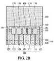
- FIGS. 2A and 2Bshow exemplary side views of the compact camera module shown in FIG. 1 ;
- FIG. 3shows a schematic cross-section of a compact camera module of a second embodiment of the invention.
- FIG. 4shows a schematic cross-section of a compact camera module of a third embodiment of the invention.
- FIG. 1is a schematic cross-section of a compact camera module of a first embodiment of the invention.
- FIGS. 2A and 2Bare exemplary side views of the compact camera module shown in FIG. 1 .
- the compact camera modulecomprises an image sensing device, a set of optical elements 140 , and a zooming device 150 .
- the image sensing devicecomprises a chip scale package having an image sensor array chip 100 , a package layer 110 , a trace set 120 (see FIG. 2A or 2 B), and a transparent substrate 130 .
- the image sensor array chip 100comprises an image sensor array 105 on a top surface 100 a thereof.
- the image sensor array chip 100is made of a semiconductor substrate such as elemental or compound semiconductors.
- the image sensor array chip 100is made of a single crystalline silicon substrate with predetermined electron components (not shown), interconnection wirings (not shown), and the image sensor array 105 .
- the image sensor array 105is a photosensitive component, such as an array of photodiodes in this embodiment for sensing incident light and generating corresponding electronic signals.
- the package layer 110underlies side surfaces 100 b and a bottom surface 100 c of the image sensor array chip 100 .
- the package layer 110comprises an adhesion layer 111 , such as epoxy, underlying the side surfaces 100 b and the bottom surface 100 c of the image sensor array chip 100 , and a substrate layer 112 underlying the adhesion layer 111 .
- the trace set 120comprises a plurality of first traces 121 and at least one second trace 122 extending from the top surface 100 a of the image sensor array chip 100 via side surfaces 110 b of the package layer 110 to a bottom surface 110 c of the package layer 110 .
- the plurality of first traces 121conducts the electronic signals generated by the image sensor array 105 and ground connection for the image sensor array chip 100
- the at least one second trace 122is electrically joined to the zooming device 150 .
- a formation method for the trace setis known by those skilled in the art (referring to U.S. Pat. No. 6,777,767 disclosed by Badehi, for example), and thus, is omitted herein.
- a plurality of optional solder balls or bumps 180are respectively attached to ends of the plurality of first traces 121 and the at least one second trace 122 underlying the package layer 110 for signal input/output and ground connection.
- the transparent substrate 130covers the top surface 100 a of the image sensor array chip 100 . More specifically, the transparent substrate 130 covers the image sensor array 105 of the image sensor array chip 100 .
- the transparent substrate 130can be glass, quartz, or other appropriate transparent materials. In this embodiment the transparent substrate 130 is glass, attached to and spaced from the image sensor array chip 100 by spacers 135 .
- the set of optical elements 140connects to the image sensing device, and comprises a lens set 141 . More specifically, the set of optical elements 140 overlies the transparent substrate 130 , and aligns with the image sensor array 105 .
- the set of optical elements 140further comprises a housing 143 , a supporter set 142 , and an aperture opening 144 .
- the housing 143is connected to the transparent substrate 130 of the image sensing device and supports the lens set 141 .
- the housing 143can be optionally coated by an opaque coating (not shown) to prevent unwanted light incidence into the image sensing device.
- the supporter set 142holds and connects the lens set 141 to the housing 143 .
- the aperture opening 144exposes the lens set 141 and the image sensor array 105 to the environment for light incident.
- the set of optical elements 141comprises a set of convex lenses 141 a and 141 b.
- the set of optical elements 141may comprise one single lens or more than two lenses, and the lens type can be properly selected as needed.
- the supporter set 142comprises a supporter 142 a connecting the lens 141 a of the set of optical elements 141 to the housing 143 and aligning the lens 141 a with the image sensor array 105 , and a supporter 142 b connecting the lens 141 b of the set of optical elements 141 to the housing 143 and aligning the lens 141 b with the image sensor array 105 and the lens 141 a.
- the lenses 141 a and 141 bmay directly connect to the housing 143 without any supporters.
- the zooming device 150connects to the set of optical elements 140 for adjusting a distance between the lens set 141 and the image sensing device; more specifically, the image sensor array 105 .
- the zooming device 150directly electrically joins with the image sensing device, and thus, the image sensing device can directly control the operation of the zooming device 150 . More specifically, the image sensing device controls the zooming device 150 to move back and forth along a direction shown by an arrow A in FIG. 1 for zooming for image capture of the image sensor array 105 of the image sensing devices.
- the zooming device 150can be selected from a group consisting of a piezo motor, a stepping motor, and a voice coil motor for the aforementioned operation.
- the zooming device 150further comprises at least one extension part 151 directly electrically connected to the at least one second trace 122 of the image sensing device, and a housing 152 connected to the image sensing device and the set of optical elements 140 .
- the image sensing devicemay transfer signals to the zooming device 150 via the at least one second trace 122 and the at least one extension part 151 for controlling the zooming operation of the zooming device 150 .
- the signal transfer pathcan be shortened, and thus, product performance can be improved.
- the zooming device 150directly electrically joins with the image sensing device, so a conventional cable, flexible printed circuit board, and encapsulating material are no longer required.
- the assembly process and structure of the image sensing device and the zooming device 150is simplified, product size can be decreased, and product yield can be improved.
- the zooming device 150directly electrically joins with the image sensing device at a position between the package layer 110 and the transparent substrate 130 . More specifically, when considering the extension path of the at least one second trace 122 of the image sensing device, the zooming device 150 directly electrically joins with the image sensing device at a position between side surfaces 110 b and 130 b of the package layer 110 and the transparent substrate 130 .
- the at least one extension part 151 of the zooming device 150may extend along the side surface 130 b of the transparent substrate 130 to the position between side surfaces 110 b and 130 b of the package layer 110 and the transparent substrate 130 , and directly electrically contacts the at least one second trace 122 of the trace set 120 of the image sensing device.
- the at least one second trace 122is directly electrically joined to the zooming device 150 , more specifically the at least one extension part 151 , by a connection component 160 , such as by solder, a retaining clamp, a thimble, or an anisotropic conduction paste for solid connection therebetween and/or decrease of contact resistance thereof.
- a connection component 160such as by solder, a retaining clamp, a thimble, or an anisotropic conduction paste for solid connection therebetween and/or decrease of contact resistance thereof.
- FIGS. 2A and 2Bshow exemplary side views of the compact camera module along the arrow B shown in FIG. 1 .
- the plurality of first traces 121 and the at least one second trace 122 of the trace set 120are all kept exposed prior to assembly of the image sensing device and the zooming device 150 , and then the at least one second trace 122 and the zooming device 150 , more specifically the at least one extension part 151 , are electrically joined.
- the plurality of first traces 121are respectively sealed by insulating material 170 at the position between side surfaces 110 b and 130 b (see FIG. 1 ) of the package layer 110 and the transparent substrate 130 .
- the plurality of first traces 121are protected from corrosion and peeling due to moisture penetration from the environment.
- the at least one second trace 122 and the zooming device 150are electrically joined, and the joint can also protect the at least one second trace 122 from corrosion and peeling due to moisture penetration from the environment.
- FIG. 3is a cross section of a compact camera module of a second embodiment of the invention.
- the compact camera module of this embodimentis nearly identical to that of the first embodiment, and for brevity, detailed descriptions of identical portions are omitted.
- the compact camera module of this embodimentis different from the first embodiment in the extension paths of the plurality of first traces 121 and the at least one second trace 122 of the trace set 120 .
- the compact camera module of the second embodimentfurther comprises a through hole set comprising a plurality of first through holes 101 and at least one second through hole 102 passing through the image sensor array chip 100 beyond the image sensor array 105 .
- the plurality of first traces 121respectively extend from the top surface 100 a of the image sensor array chip 100 via the plurality of first through holes 101 to a bottom surface 100 c of the image sensor array chip 100 .
- the at least one second trace 122extends from the top surface 100 a of the image sensor array chip 100 via the at least one second through hole 102 to the bottom surface 100 c of the image sensor array chip 100 .
- a plurality of optional solder balls or bumps 180are respectively attached to ends of the plurality of first traces 121 and the at least one second trace 122 on the bottom surface 100 c of the image sensor array chip 100 for signal input/output and ground connection.
- the package layer 110 shown in FIG. 1 of the compact camera module of the first embodimentis not required.
- the package layer 110 shown in FIG. 1can be optionally disposed as shown in FIG. 1 , and the through hole set and the trace set 120 further extend to the bottom of the package layer 110 .
- the at least one second trace 122further extends through the top surface 100 a of the image sensor array chip 100 to a position between side surfaces 100 b and 130 b of the image sensor array chip 100 and the transparent substrate 130 .
- the zooming device 150more specifically the at least one extension part 151 , further extends along the side surface 130 b of the transparent substrate 130 and electrically contacts with the at least one second trace 122 as described for FIGS. 1 , 2 A and 2 B.
- FIG. 4is a cross section of a compact camera module of a third embodiment of the invention.
- the compact camera module of this embodimentis nearly identical to that of the second embodiment, and for brevity, detailed descriptions of identical portions are omitted.
- the compact camera module of this embodimentis different from the second embodiment in that the zooming device 150 , more specifically the at least one extension part 151 , extends through the transparent substrate 130 and directly electrically joins with the at least one second trace 122 .
- the at least one second trace 122is not required to be extended through the top surface 100 a of the image sensor array chip 100 to the position between side surfaces 100 b and 130 b of the image sensor array chip 100 and the transparent substrate 130 .
- the at least one second trace 122is directly electrically joined to the zooming device 150 , more specifically the at least one extension part 151 , by a connection component 160 , such as by solder or an anisotropic conduction paste for solid connection therebetween and/or decrease of contact resistance thereof.
Landscapes
- Engineering & Computer Science (AREA)
- Multimedia (AREA)
- Signal Processing (AREA)
- Physics & Mathematics (AREA)
- General Physics & Mathematics (AREA)
- Transforming Light Signals Into Electric Signals (AREA)
- Lens Barrels (AREA)
- Studio Devices (AREA)
Abstract
Description
- 1. Field of the Invention
- The invention relates to photosensitive devices and more particularly to compact camera modules.
- 2. Description of the Related Art
- A machine component of a conventional automatic focus compact camera module and zoom compact camera module is electrically connected to an external circuit board by a cable or a flexible printed circuit board. The external circuit board is electrically connected to an image sensor, and thus, the image sensor and the corresponding compact camera module are indirectly electrically connected. The electrical connections between conventional compact camera modules are complicated and an encapsulating material is required to assemble the conventional compact camera module and the corresponding image sensor. As a result, process costs are relatively high and product size is relatively larger, such that device performance and yield are negatively affected.
- Thus, a novel compact camera module is required to solve the described problems.
- An embodiment of the invention provides a compact camera module. The compact camera module includes an image sensing device, a set of optical elements, and a zooming device. The set of optical elements connects to the image sensing device, and comprises a lens set. The zooming device connects to the set of optical elements for adjusting a distance between the lens set and the image sensing device. The zooming device directly electrically joins with the image sensing device.
- An embodiment of the invention provides another compact camera module. The image sensor device includes an image sensor array chip, a package layer, a trace set, a transparent substrate, a set of optical elements, and a zooming device. The image sensor array chip comprises an image sensor array on a top surface thereof. The package layer underlies side surfaces and a bottom surface of the image sensor array chip. The trace set comprises a plurality of first traces and at least one second trace extending from the top surface of the image sensor array chip via side surfaces of the package layer to a bottom surface of the package layer. The transparent substrate covers the top surface of the image sensor array chip. The set of optical elements overlies the transparent substrate, aligns with the image sensor array, and comprises a lens set. The zooming device connects to the set of optical elements for adjusting a distance between the lens set and the image sensor array. The zooming device directly electrically joins with the at least one second trace.
- An embodiment of the invention provides another compact camera module. The image sensor device includes an image sensor array chip, a through hole set, a trace set, a transparent substrate, a set of optical elements, and a zooming device. The image sensor array chip comprises an image sensor array on a top surface thereof. The through hole set comprises a plurality of first through holes and at least one second through hole passing through the image sensor array chip beyond the image sensor array. The trace set comprises a plurality of first traces and at least one second trace, wherein the plurality of first traces respectively extend from the top surface of the image sensor array chip via side surfaces of the first through holes to a bottom surface of the image sensor array chip, and the at least one second trace extend from the top surface of the image sensor array chip via side surfaces of the at least one through hole to the bottom surface of the image sensor array chip. The transparent substrate covers the top surface of the image sensor array chip. The set of optical elements overlies the transparent substrate, aligns with the image sensor array, and comprises a lens set. The zooming device connects to the set of optical elements for adjusting a distance between the lens set and the image sensor array. The zooming device directly electrically joins with the at least one second trace.
- Further scope of the applicability of the invention will become apparent from the detailed descriptions given hereinafter. It should be understood however, that the detailed descriptions and specific examples, while indicating preferred embodiments of the invention, are given by way of illustration only, as various changes and modifications within the spirit and scope of the invention will become apparent to those skilled in the Art from the detailed descriptions.
- A detailed description is given in the following embodiments with reference to the accompanying drawings.
- The invention can be more fully understood by reading the subsequent detailed description and examples with references made to the accompanying drawings, wherein:
FIG. 1 shows a schematic cross-section of a compact camera module of a first embodiment of the invention;FIGS. 2A and 2B show exemplary side views of the compact camera module shown inFIG. 1 ;FIG. 3 shows a schematic cross-section of a compact camera module of a second embodiment of the invention; andFIG. 4 shows a schematic cross-section of a compact camera module of a third embodiment of the invention.- The following description is of the best-contemplated mode of carrying out the invention. This description is made for the purpose of illustrating the general principles of the invention and should not be taken in a limiting sense. The scope of the invention is best determined by reference to the appended claims.
- Next, the concepts and specific practice modes of the invention is detailedly described by the embodiments and the attached drawings. In the drawings or description, similar elements are indicated by similar reference numerals and/or letters. Further, the element shape or thickness in the drawings can be expanded for simplification or convenience of indication. Moreover, elements which are not shown or described can be in every form known by those skilled in the art.
- Specific embodiments of the invention for fabrication of a chip scale package comprising an image sensor array chip are described. It is noted that the concepts of the invention can be applied to any known or newly developed package types of the image sensor array chip.
FIG. 1 is a schematic cross-section of a compact camera module of a first embodiment of the invention.FIGS. 2A and 2B are exemplary side views of the compact camera module shown inFIG. 1 . Referring toFIG. 1 , the compact camera module comprises an image sensing device, a set ofoptical elements 140, and azooming device 150.- In this embodiment, the image sensing device comprises a chip scale package having an image
sensor array chip 100, apackage layer 110, a trace set120 (seeFIG. 2A or2B), and atransparent substrate 130. The imagesensor array chip 100 comprises animage sensor array 105 on atop surface 100athereof. The imagesensor array chip 100 is made of a semiconductor substrate such as elemental or compound semiconductors. In this embodiment, the imagesensor array chip 100 is made of a single crystalline silicon substrate with predetermined electron components (not shown), interconnection wirings (not shown), and theimage sensor array 105. Theimage sensor array 105 is a photosensitive component, such as an array of photodiodes in this embodiment for sensing incident light and generating corresponding electronic signals. - The
package layer 110 underlies side surfaces100band abottom surface 100cof the imagesensor array chip 100. In this embodiment, thepackage layer 110 comprises anadhesion layer 111, such as epoxy, underlying the side surfaces100band thebottom surface 100cof the imagesensor array chip 100, and asubstrate layer 112 underlying theadhesion layer 111. - Referring to
FIG. 1 andFIG. 2A or2B, the trace set120 comprises a plurality offirst traces 121 and at least onesecond trace 122 extending from thetop surface 100aof the imagesensor array chip 100 via side surfaces110bof thepackage layer 110 to abottom surface 110cof thepackage layer 110. In this embodiment, the plurality offirst traces 121 conducts the electronic signals generated by theimage sensor array 105 and ground connection for the imagesensor array chip 100, and the at least onesecond trace 122 is electrically joined to thezooming device 150. A formation method for the trace set is known by those skilled in the art (referring to U.S. Pat. No. 6,777,767 disclosed by Badehi, for example), and thus, is omitted herein. In this embodiment, a plurality of optional solder balls or bumps180 are respectively attached to ends of the plurality offirst traces 121 and the at least onesecond trace 122 underlying thepackage layer 110 for signal input/output and ground connection. - The
transparent substrate 130 covers thetop surface 100aof the imagesensor array chip 100. More specifically, thetransparent substrate 130 covers theimage sensor array 105 of the imagesensor array chip 100. Thetransparent substrate 130 can be glass, quartz, or other appropriate transparent materials. In this embodiment thetransparent substrate 130 is glass, attached to and spaced from the imagesensor array chip 100 byspacers 135. - In
FIG. 1 , the set ofoptical elements 140 connects to the image sensing device, and comprises alens set 141. More specifically, the set ofoptical elements 140 overlies thetransparent substrate 130, and aligns with theimage sensor array 105. In this embodiment, the set ofoptical elements 140 further comprises ahousing 143, asupporter set 142, and anaperture opening 144. Thehousing 143 is connected to thetransparent substrate 130 of the image sensing device and supports thelens set 141. Thehousing 143 can be optionally coated by an opaque coating (not shown) to prevent unwanted light incidence into the image sensing device. The supporter set142 holds and connects the lens set141 to thehousing 143. Theaperture opening 144 exposes the lens set141 and theimage sensor array 105 to the environment for light incident. - In this embodiment, the set of
optical elements 141 comprises a set ofconvex lenses optical elements 141 may comprise one single lens or more than two lenses, and the lens type can be properly selected as needed. In this embodiment, the supporter set142 comprises asupporter 142aconnecting thelens 141aof the set ofoptical elements 141 to thehousing 143 and aligning thelens 141awith theimage sensor array 105, and asupporter 142bconnecting thelens 141bof the set ofoptical elements 141 to thehousing 143 and aligning thelens 141bwith theimage sensor array 105 and thelens 141a.In other embodiments, thelenses housing 143 without any supporters. - Referring to
FIG. 1 andFIG. 2A or2B, thezooming device 150 connects to the set ofoptical elements 140 for adjusting a distance between the lens set141 and the image sensing device; more specifically, theimage sensor array 105. Thezooming device 150 directly electrically joins with the image sensing device, and thus, the image sensing device can directly control the operation of thezooming device 150. More specifically, the image sensing device controls thezooming device 150 to move back and forth along a direction shown by an arrow A inFIG. 1 for zooming for image capture of theimage sensor array 105 of the image sensing devices. Thezooming device 150 can be selected from a group consisting of a piezo motor, a stepping motor, and a voice coil motor for the aforementioned operation. - In this embodiment, the
zooming device 150 further comprises at least oneextension part 151 directly electrically connected to the at least onesecond trace 122 of the image sensing device, and ahousing 152 connected to the image sensing device and the set ofoptical elements 140. Thus, the image sensing device may transfer signals to thezooming device 150 via the at least onesecond trace 122 and the at least oneextension part 151 for controlling the zooming operation of thezooming device 150. As compared with the prior art, the signal transfer path can be shortened, and thus, product performance can be improved. Further, thezooming device 150 directly electrically joins with the image sensing device, so a conventional cable, flexible printed circuit board, and encapsulating material are no longer required. Thus, the assembly process and structure of the image sensing device and thezooming device 150 is simplified, product size can be decreased, and product yield can be improved. - In this embodiment, the
zooming device 150 directly electrically joins with the image sensing device at a position between thepackage layer 110 and thetransparent substrate 130. More specifically, when considering the extension path of the at least onesecond trace 122 of the image sensing device, thezooming device 150 directly electrically joins with the image sensing device at a position betweenside surfaces package layer 110 and thetransparent substrate 130. For example, the at least oneextension part 151 of thezooming device 150 may extend along theside surface 130bof thetransparent substrate 130 to the position betweenside surfaces package layer 110 and thetransparent substrate 130, and directly electrically contacts the at least onesecond trace 122 of the trace set120 of the image sensing device. In other embodiments, the at least onesecond trace 122 is directly electrically joined to thezooming device 150, more specifically the at least oneextension part 151, by aconnection component 160, such as by solder, a retaining clamp, a thimble, or an anisotropic conduction paste for solid connection therebetween and/or decrease of contact resistance thereof. FIGS. 2A and 2B show exemplary side views of the compact camera module along the arrow B shown inFIG. 1 . Referring toFIG. 2A , the plurality offirst traces 121 and the at least onesecond trace 122 of the trace set120 are all kept exposed prior to assembly of the image sensing device and thezooming device 150, and then the at least onesecond trace 122 and thezooming device 150, more specifically the at least oneextension part 151, are electrically joined. In other embodiments as shown inFIG. 2B , for example, the plurality offirst traces 121 are respectively sealed by insulatingmaterial 170 at the position betweenside surfaces FIG. 1 ) of thepackage layer 110 and thetransparent substrate 130. Thus, the plurality offirst traces 121 are protected from corrosion and peeling due to moisture penetration from the environment. The at least onesecond trace 122 and thezooming device 150, more specifically the at least oneextension part 151, are electrically joined, and the joint can also protect the at least onesecond trace 122 from corrosion and peeling due to moisture penetration from the environment.FIG. 3 is a cross section of a compact camera module of a second embodiment of the invention. The compact camera module of this embodiment is nearly identical to that of the first embodiment, and for brevity, detailed descriptions of identical portions are omitted. The compact camera module of this embodiment is different from the first embodiment in the extension paths of the plurality offirst traces 121 and the at least onesecond trace 122 of the trace set120.- More specifically, the compact camera module of the second embodiment further comprises a through hole set comprising a plurality of first through
holes 101 and at least one second throughhole 102 passing through the imagesensor array chip 100 beyond theimage sensor array 105. The plurality offirst traces 121 respectively extend from thetop surface 100aof the imagesensor array chip 100 via the plurality of first throughholes 101 to abottom surface 100cof the imagesensor array chip 100. The at least onesecond trace 122 extends from thetop surface 100aof the imagesensor array chip 100 via the at least one second throughhole 102 to thebottom surface 100cof the imagesensor array chip 100. In this embodiment, a plurality of optional solder balls or bumps180 are respectively attached to ends of the plurality offirst traces 121 and the at least onesecond trace 122 on thebottom surface 100cof the imagesensor array chip 100 for signal input/output and ground connection. Thus, thepackage layer 110 shown inFIG. 1 of the compact camera module of the first embodiment is not required. In some cases, thepackage layer 110 shown inFIG. 1 can be optionally disposed as shown inFIG. 1 , and the through hole set and the trace set120 further extend to the bottom of thepackage layer 110. - In this embodiment, the at least one
second trace 122 further extends through thetop surface 100aof the imagesensor array chip 100 to a position betweenside surfaces 100band130bof the imagesensor array chip 100 and thetransparent substrate 130. Thus, thezooming device 150, more specifically the at least oneextension part 151, further extends along theside surface 130bof thetransparent substrate 130 and electrically contacts with the at least onesecond trace 122 as described forFIGS. 1 ,2A and2B. FIG. 4 is a cross section of a compact camera module of a third embodiment of the invention. The compact camera module of this embodiment is nearly identical to that of the second embodiment, and for brevity, detailed descriptions of identical portions are omitted. The compact camera module of this embodiment is different from the second embodiment in that thezooming device 150, more specifically the at least oneextension part 151, extends through thetransparent substrate 130 and directly electrically joins with the at least onesecond trace 122. Thus, the at least onesecond trace 122 is not required to be extended through thetop surface 100aof the imagesensor array chip 100 to the position betweenside surfaces 100band130bof the imagesensor array chip 100 and thetransparent substrate 130. In other embodiments, the at least onesecond trace 122 is directly electrically joined to thezooming device 150, more specifically the at least oneextension part 151, by aconnection component 160, such as by solder or an anisotropic conduction paste for solid connection therebetween and/or decrease of contact resistance thereof.- While the invention has been described by way of example and in terms of preferred embodiment, it is to be understood that the invention is not limited thereto. To the contrary, it is intended to cover various modifications and similar arrangements (as would be apparent to those skilled in the Art). Therefore, the scope of the appended claims should be accorded the broadest interpretation so as to encompass all such modifications and similar arrangements.
Claims (17)
Priority Applications (3)
| Application Number | Priority Date | Filing Date | Title |
|---|---|---|---|
| US12/399,706US8355628B2 (en) | 2009-03-06 | 2009-03-06 | Compact camera module |
| TW098123869ATWI417629B (en) | 2009-03-06 | 2009-07-15 | Compact camera module |
| CN2009101651920ACN101827208B (en) | 2009-03-06 | 2009-07-27 | tiny camera module |
Applications Claiming Priority (1)
| Application Number | Priority Date | Filing Date | Title |
|---|---|---|---|
| US12/399,706US8355628B2 (en) | 2009-03-06 | 2009-03-06 | Compact camera module |
Publications (2)
| Publication Number | Publication Date |
|---|---|
| US20100226633A1true US20100226633A1 (en) | 2010-09-09 |
| US8355628B2 US8355628B2 (en) | 2013-01-15 |
Family
ID=42678330
Family Applications (1)
| Application Number | Title | Priority Date | Filing Date |
|---|---|---|---|
| US12/399,706Active2029-04-14US8355628B2 (en) | 2009-03-06 | 2009-03-06 | Compact camera module |
Country Status (3)
| Country | Link |
|---|---|
| US (1) | US8355628B2 (en) |
| CN (1) | CN101827208B (en) |
| TW (1) | TWI417629B (en) |
Cited By (4)
| Publication number | Priority date | Publication date | Assignee | Title |
|---|---|---|---|---|
| US20110037886A1 (en)* | 2009-08-14 | 2011-02-17 | Harpuneet Singh | Wafer level camera module with molded housing and method of manufacturing |
| EP2575176A3 (en)* | 2011-09-29 | 2013-05-01 | Flextronics Ap, Llc | Folded tape package for electronic devices |
| US20130141626A1 (en)* | 2010-08-23 | 2013-06-06 | Canon Kabushiki Kaisha | Image pickup device, image pickup module, and camera |
| TWI575303B (en)* | 2014-05-13 | 2017-03-21 | 豪威科技股份有限公司 | Suspension lens system and wafer level method for manufacturing suspension lens system |
Families Citing this family (3)
| Publication number | Priority date | Publication date | Assignee | Title |
|---|---|---|---|---|
| US8837060B2 (en) | 2011-02-25 | 2014-09-16 | Visera Technologies Company Limited | Image capture lens module and wafer level packaged image capture devices |
| US20170280034A1 (en)* | 2016-03-23 | 2017-09-28 | Magna Electronics Inc. | Vehicle vision system camera with enhanced imager and lens assembly |
| TWI799943B (en)* | 2021-08-12 | 2023-04-21 | 致伸科技股份有限公司 | Lens module and manufacturing method used therein |
Citations (18)
| Publication number | Priority date | Publication date | Assignee | Title |
|---|---|---|---|---|
| US5008582A (en)* | 1988-01-29 | 1991-04-16 | Kabushiki Kaisha Toshiba | Electronic device having a cooling element |
| US20040041282A1 (en)* | 2002-08-29 | 2004-03-04 | Kinsman Larry D. | Flip-chip image sensor packages and methods of fabrication |
| US6777767B2 (en)* | 1999-12-10 | 2004-08-17 | Shellcase Ltd. | Methods for producing packaged integrated circuit devices & packaged integrated circuit devices produced thereby |
| US20050259174A1 (en)* | 2004-05-21 | 2005-11-24 | Matsushita Electric Industrial Co., Ltd. | Solid state imaging device and method for producing the same |
| US20060138905A1 (en)* | 2004-12-28 | 2006-06-29 | Gonzales Christopher A | Piezoelectric fan for an integrated circuit chip |
| US20060152615A1 (en)* | 2005-01-07 | 2006-07-13 | Yong-Chai Kwon | Image sensor chip having plate, wafer assembly and manufacturing method for the same |
| WO2006106953A1 (en)* | 2005-04-01 | 2006-10-12 | Matsushita Electric Industrial Co., Ltd. | Image pickup device |
| US7167376B2 (en)* | 2003-05-19 | 2007-01-23 | Fuji Photo Film Co., Ltd. | Multilayer wiring board, method of mounting components, and image pick-up device |
| US20070147816A1 (en)* | 2005-12-27 | 2007-06-28 | Tessera, Inc. | Camera modules with liquid optical elements |
| US20070154198A1 (en)* | 2003-12-19 | 2007-07-05 | Hysonic Co., Ltd. | Image photographing apparatus |
| US20070278701A1 (en)* | 2006-06-02 | 2007-12-06 | Siliconware Precision Industries Co., Ltd. | Semiconductor package and method for fabricating the same |
| US7359631B2 (en)* | 2004-09-22 | 2008-04-15 | Fujifilm Corporation | Lens driving device, imaging device using the same, and small-sized electronics device using the same |
| US20080142917A1 (en)* | 2006-12-14 | 2008-06-19 | Samsung Electro-Mechanics Co., Ltd. | Image sensor module, method of manufacturing the same, and camera module having the same |
| US20080164553A1 (en)* | 2007-01-04 | 2008-07-10 | Visera Technologies Company Limited | Isolation structures for CMOS image sensor chip scale packages |
| US20080217715A1 (en)* | 2005-10-11 | 2008-09-11 | Park Tae-Seok | Wafer Level Package Using Silicon Via Contacts for Cmos Image Sensor and Method of Fabricating the Same |
| US7665915B2 (en)* | 2006-03-23 | 2010-02-23 | Lg Innotek Co., Ltd. | Camera module, method of manufacturing the same, and printed circuit board for the camera module |
| US7683960B2 (en)* | 2003-03-25 | 2010-03-23 | Fujinon Corporation | Double-sealed imaging apparatus |
| US7863724B2 (en)* | 2008-02-12 | 2011-01-04 | International Business Machines Corporation | Circuit substrate having post-fed die side power supply connections |
Family Cites Families (2)
| Publication number | Priority date | Publication date | Assignee | Title |
|---|---|---|---|---|
| CN1858975B (en)* | 2005-05-08 | 2010-12-01 | 吉佳科技股份有限公司 | Voice coil motor device |
| CN2890964Y (en)* | 2006-04-04 | 2007-04-18 | 新钜科技股份有限公司 | Improved miniature camera barrel mount |
- 2009
- 2009-03-06USUS12/399,706patent/US8355628B2/enactiveActive
- 2009-07-15TWTW098123869Apatent/TWI417629B/enactive
- 2009-07-27CNCN2009101651920Apatent/CN101827208B/enactiveActive
Patent Citations (19)
| Publication number | Priority date | Publication date | Assignee | Title |
|---|---|---|---|---|
| US5008582A (en)* | 1988-01-29 | 1991-04-16 | Kabushiki Kaisha Toshiba | Electronic device having a cooling element |
| US6777767B2 (en)* | 1999-12-10 | 2004-08-17 | Shellcase Ltd. | Methods for producing packaged integrated circuit devices & packaged integrated circuit devices produced thereby |
| US20040041282A1 (en)* | 2002-08-29 | 2004-03-04 | Kinsman Larry D. | Flip-chip image sensor packages and methods of fabrication |
| US7683960B2 (en)* | 2003-03-25 | 2010-03-23 | Fujinon Corporation | Double-sealed imaging apparatus |
| US7167376B2 (en)* | 2003-05-19 | 2007-01-23 | Fuji Photo Film Co., Ltd. | Multilayer wiring board, method of mounting components, and image pick-up device |
| US20070154198A1 (en)* | 2003-12-19 | 2007-07-05 | Hysonic Co., Ltd. | Image photographing apparatus |
| US20050259174A1 (en)* | 2004-05-21 | 2005-11-24 | Matsushita Electric Industrial Co., Ltd. | Solid state imaging device and method for producing the same |
| US7359631B2 (en)* | 2004-09-22 | 2008-04-15 | Fujifilm Corporation | Lens driving device, imaging device using the same, and small-sized electronics device using the same |
| US20060138905A1 (en)* | 2004-12-28 | 2006-06-29 | Gonzales Christopher A | Piezoelectric fan for an integrated circuit chip |
| US20060152615A1 (en)* | 2005-01-07 | 2006-07-13 | Yong-Chai Kwon | Image sensor chip having plate, wafer assembly and manufacturing method for the same |
| WO2006106953A1 (en)* | 2005-04-01 | 2006-10-12 | Matsushita Electric Industrial Co., Ltd. | Image pickup device |
| US20090213232A1 (en)* | 2005-04-01 | 2009-08-27 | Matsushita Electric Industrial Co., Ltd. | Image pickup device |
| US20080217715A1 (en)* | 2005-10-11 | 2008-09-11 | Park Tae-Seok | Wafer Level Package Using Silicon Via Contacts for Cmos Image Sensor and Method of Fabricating the Same |
| US20070147816A1 (en)* | 2005-12-27 | 2007-06-28 | Tessera, Inc. | Camera modules with liquid optical elements |
| US7665915B2 (en)* | 2006-03-23 | 2010-02-23 | Lg Innotek Co., Ltd. | Camera module, method of manufacturing the same, and printed circuit board for the camera module |
| US20070278701A1 (en)* | 2006-06-02 | 2007-12-06 | Siliconware Precision Industries Co., Ltd. | Semiconductor package and method for fabricating the same |
| US20080142917A1 (en)* | 2006-12-14 | 2008-06-19 | Samsung Electro-Mechanics Co., Ltd. | Image sensor module, method of manufacturing the same, and camera module having the same |
| US20080164553A1 (en)* | 2007-01-04 | 2008-07-10 | Visera Technologies Company Limited | Isolation structures for CMOS image sensor chip scale packages |
| US7863724B2 (en)* | 2008-02-12 | 2011-01-04 | International Business Machines Corporation | Circuit substrate having post-fed die side power supply connections |
Cited By (7)
| Publication number | Priority date | Publication date | Assignee | Title |
|---|---|---|---|---|
| US20110037886A1 (en)* | 2009-08-14 | 2011-02-17 | Harpuneet Singh | Wafer level camera module with molded housing and method of manufacturing |
| US9419032B2 (en)* | 2009-08-14 | 2016-08-16 | Nanchang O-Film Optoelectronics Technology Ltd | Wafer level camera module with molded housing and method of manufacturing |
| US20130141626A1 (en)* | 2010-08-23 | 2013-06-06 | Canon Kabushiki Kaisha | Image pickup device, image pickup module, and camera |
| US9111826B2 (en)* | 2010-08-23 | 2015-08-18 | Canon Kabushiki Kaisha | Image pickup device, image pickup module, and camera |
| EP2575176A3 (en)* | 2011-09-29 | 2013-05-01 | Flextronics Ap, Llc | Folded tape package for electronic devices |
| US8913180B2 (en) | 2011-09-29 | 2014-12-16 | Flextronics Ap, Llc | Folded tape package for electronic devices |
| TWI575303B (en)* | 2014-05-13 | 2017-03-21 | 豪威科技股份有限公司 | Suspension lens system and wafer level method for manufacturing suspension lens system |
Also Published As
| Publication number | Publication date |
|---|---|
| TW201033717A (en) | 2010-09-16 |
| US8355628B2 (en) | 2013-01-15 |
| TWI417629B (en) | 2013-12-01 |
| CN101827208A (en) | 2010-09-08 |
| CN101827208B (en) | 2012-11-21 |
Similar Documents
| Publication | Publication Date | Title |
|---|---|---|
| US8355628B2 (en) | Compact camera module | |
| CN101432759B (en) | System and method for mounting an image record device on a flexible substrate | |
| JP4981129B2 (en) | Camera module with pre-formed lens housing and method for manufacturing the same | |
| KR100614476B1 (en) | Camera module and camera-module manufacturing method | |
| US8823872B2 (en) | Image pickup module with improved flatness of image sensor and via electrodes | |
| KR100546411B1 (en) | Flip chip package, image sensor module including the package, and manufacturing method thereof | |
| US8194162B2 (en) | Imaging device | |
| US8606057B1 (en) | Opto-electronic modules including electrically conductive connections for integration with an electronic device | |
| US8223248B2 (en) | Image sensor module having a semiconductor chip, a holder and a coupling member | |
| US20040256687A1 (en) | Optical module, method of manufacturing the same, and electronic instrument | |
| US20050059269A1 (en) | Connector and image sensor module using the same | |
| JP2010034668A (en) | Solid-state imaging device and electronic apparatus equipped with the same | |
| CN109417081B (en) | Chip packaging structure, method and electronic equipment | |
| CN111371975A (en) | Camera module packaging structure | |
| TWI543613B (en) | Image sensor module | |
| US20040234190A1 (en) | Optical modules and method for manufacturing the same, and electronic devices | |
| US20120007148A1 (en) | Solid-state image pickup device and method for manufacturing same | |
| TWI728737B (en) | Camera module package structure | |
| JP2015088498A (en) | Solid-state imaging device and electronic camera | |
| JP5479972B2 (en) | Imaging device | |
| KR100764410B1 (en) | Image sensor module and manufacturing method | |
| TWM597983U (en) | Camera module packaging structure | |
| KR100990397B1 (en) | Wafer level image sensor module and manufacturing method thereof and camera module using same | |
| CN209104140U (en) | Chip package structure and electronic equipment | |
| JP2006157030A (en) | Solid-state imaging apparatus and manufacturing method of solid-state imaging apparatus |
Legal Events
| Date | Code | Title | Description |
|---|---|---|---|
| AS | Assignment | Owner name:VISERA TECHNOLOGIES COMPANY LIMITED, TAIWAN Free format text:ASSIGNMENT OF ASSIGNORS INTEREST;ASSIGNORS:SHIUNG, SHIN-CHANG;CHENG, CHIEH-YUAN;TSENG, LI-HSIN;REEL/FRAME:022360/0657 Effective date:20090226 | |
| AS | Assignment | Owner name:OMNIVISION TECHNOLOGIES, INC., CALIFORNIA Free format text:ASSIGNMENT OF ASSIGNORS INTEREST;ASSIGNOR:VISERA TECHNOLOGIES COMPANY LIMITED;REEL/FRAME:026563/0895 Effective date:20110624 | |
| AS | Assignment | Owner name:OMNIVISION TECHNOLOGIES, INC., CALIFORNIA Free format text:CORRECTIVE ASSIGNMENT TO CORRECT THE ASSIGNEE PREVIOUSLY RECORDED ON REEL 026563 FRAME 0895. ASSIGNOR(S) HEREBY CONFIRMS THE ASSIGNEES ARE OMNIVISION TECHNOLOGIES, INC. AND VISERA TECHNOLOGIES COMPANY LIMITED;ASSIGNOR:VISERA TECHNOLOGIES COMPANY LIMITED;REEL/FRAME:026736/0545 Effective date:20110624 Owner name:VISERA TECHNOLOGIES COMPANY LIMITED, TAIWAN Free format text:CORRECTIVE ASSIGNMENT TO CORRECT THE ASSIGNEE PREVIOUSLY RECORDED ON REEL 026563 FRAME 0895. ASSIGNOR(S) HEREBY CONFIRMS THE ASSIGNEES ARE OMNIVISION TECHNOLOGIES, INC. AND VISERA TECHNOLOGIES COMPANY LIMITED;ASSIGNOR:VISERA TECHNOLOGIES COMPANY LIMITED;REEL/FRAME:026736/0545 Effective date:20110624 | |
| STCF | Information on status: patent grant | Free format text:PATENTED CASE | |
| FPAY | Fee payment | Year of fee payment:4 | |
| MAFP | Maintenance fee payment | Free format text:PAYMENT OF MAINTENANCE FEE, 8TH YEAR, LARGE ENTITY (ORIGINAL EVENT CODE: M1552); ENTITY STATUS OF PATENT OWNER: LARGE ENTITY Year of fee payment:8 | |
| MAFP | Maintenance fee payment | Free format text:PAYMENT OF MAINTENANCE FEE, 12TH YEAR, LARGE ENTITY (ORIGINAL EVENT CODE: M1553); ENTITY STATUS OF PATENT OWNER: LARGE ENTITY Year of fee payment:12 |