US20100224130A1 - Rotating substrate support and methods of use - Google Patents
Rotating substrate support and methods of useDownload PDFInfo
- Publication number
- US20100224130A1 US20100224130A1US12/779,904US77990410AUS2010224130A1US 20100224130 A1US20100224130 A1US 20100224130A1US 77990410 AUS77990410 AUS 77990410AUS 2010224130 A1US2010224130 A1US 2010224130A1
- Authority
- US
- United States
- Prior art keywords
- substrate support
- substrate
- shaft
- disposed
- seal block
- Prior art date
- Legal status (The legal status is an assumption and is not a legal conclusion. Google has not performed a legal analysis and makes no representation as to the accuracy of the status listed.)
- Abandoned
Links
Images


Classifications
- H—ELECTRICITY
- H01—ELECTRIC ELEMENTS
- H01L—SEMICONDUCTOR DEVICES NOT COVERED BY CLASS H10
- H01L21/00—Processes or apparatus adapted for the manufacture or treatment of semiconductor or solid state devices or of parts thereof
- H01L21/67—Apparatus specially adapted for handling semiconductor or electric solid state devices during manufacture or treatment thereof; Apparatus specially adapted for handling wafers during manufacture or treatment of semiconductor or electric solid state devices or components ; Apparatus not specifically provided for elsewhere
- H01L21/683—Apparatus specially adapted for handling semiconductor or electric solid state devices during manufacture or treatment thereof; Apparatus specially adapted for handling wafers during manufacture or treatment of semiconductor or electric solid state devices or components ; Apparatus not specifically provided for elsewhere for supporting or gripping
- H01L21/687—Apparatus specially adapted for handling semiconductor or electric solid state devices during manufacture or treatment thereof; Apparatus specially adapted for handling wafers during manufacture or treatment of semiconductor or electric solid state devices or components ; Apparatus not specifically provided for elsewhere for supporting or gripping using mechanical means, e.g. chucks, clamps or pinches
- H01L21/68714—Apparatus specially adapted for handling semiconductor or electric solid state devices during manufacture or treatment thereof; Apparatus specially adapted for handling wafers during manufacture or treatment of semiconductor or electric solid state devices or components ; Apparatus not specifically provided for elsewhere for supporting or gripping using mechanical means, e.g. chucks, clamps or pinches the wafers being placed on a susceptor, stage or support
- H01L21/68792—Apparatus specially adapted for handling semiconductor or electric solid state devices during manufacture or treatment thereof; Apparatus specially adapted for handling wafers during manufacture or treatment of semiconductor or electric solid state devices or components ; Apparatus not specifically provided for elsewhere for supporting or gripping using mechanical means, e.g. chucks, clamps or pinches the wafers being placed on a susceptor, stage or support characterised by the construction of the shaft
- C—CHEMISTRY; METALLURGY
- C23—COATING METALLIC MATERIAL; COATING MATERIAL WITH METALLIC MATERIAL; CHEMICAL SURFACE TREATMENT; DIFFUSION TREATMENT OF METALLIC MATERIAL; COATING BY VACUUM EVAPORATION, BY SPUTTERING, BY ION IMPLANTATION OR BY CHEMICAL VAPOUR DEPOSITION, IN GENERAL; INHIBITING CORROSION OF METALLIC MATERIAL OR INCRUSTATION IN GENERAL
- C23C—COATING METALLIC MATERIAL; COATING MATERIAL WITH METALLIC MATERIAL; SURFACE TREATMENT OF METALLIC MATERIAL BY DIFFUSION INTO THE SURFACE, BY CHEMICAL CONVERSION OR SUBSTITUTION; COATING BY VACUUM EVAPORATION, BY SPUTTERING, BY ION IMPLANTATION OR BY CHEMICAL VAPOUR DEPOSITION, IN GENERAL
- C23C16/00—Chemical coating by decomposition of gaseous compounds, without leaving reaction products of surface material in the coating, i.e. chemical vapour deposition [CVD] processes
- C23C16/44—Chemical coating by decomposition of gaseous compounds, without leaving reaction products of surface material in the coating, i.e. chemical vapour deposition [CVD] processes characterised by the method of coating
- C23C16/458—Chemical coating by decomposition of gaseous compounds, without leaving reaction products of surface material in the coating, i.e. chemical vapour deposition [CVD] processes characterised by the method of coating characterised by the method used for supporting substrates in the reaction chamber
- C23C16/4582—Rigid and flat substrates, e.g. plates or discs
- C23C16/4583—Rigid and flat substrates, e.g. plates or discs the substrate being supported substantially horizontally
- C23C16/4584—Rigid and flat substrates, e.g. plates or discs the substrate being supported substantially horizontally the substrate being rotated
- G—PHYSICS
- G02—OPTICS
- G02F—OPTICAL DEVICES OR ARRANGEMENTS FOR THE CONTROL OF LIGHT BY MODIFICATION OF THE OPTICAL PROPERTIES OF THE MEDIA OF THE ELEMENTS INVOLVED THEREIN; NON-LINEAR OPTICS; FREQUENCY-CHANGING OF LIGHT; OPTICAL LOGIC ELEMENTS; OPTICAL ANALOGUE/DIGITAL CONVERTERS
- G02F1/00—Devices or arrangements for the control of the intensity, colour, phase, polarisation or direction of light arriving from an independent light source, e.g. switching, gating or modulating; Non-linear optics
- G02F1/01—Devices or arrangements for the control of the intensity, colour, phase, polarisation or direction of light arriving from an independent light source, e.g. switching, gating or modulating; Non-linear optics for the control of the intensity, phase, polarisation or colour
- G02F1/13—Devices or arrangements for the control of the intensity, colour, phase, polarisation or direction of light arriving from an independent light source, e.g. switching, gating or modulating; Non-linear optics for the control of the intensity, phase, polarisation or colour based on liquid crystals, e.g. single liquid crystal display cells
- H—ELECTRICITY
- H01—ELECTRIC ELEMENTS
- H01L—SEMICONDUCTOR DEVICES NOT COVERED BY CLASS H10
- H01L21/00—Processes or apparatus adapted for the manufacture or treatment of semiconductor or solid state devices or of parts thereof
- H01L21/02—Manufacture or treatment of semiconductor devices or of parts thereof
- H01L21/02104—Forming layers
- H01L21/02365—Forming inorganic semiconducting materials on a substrate
- H—ELECTRICITY
- H01—ELECTRIC ELEMENTS
- H01L—SEMICONDUCTOR DEVICES NOT COVERED BY CLASS H10
- H01L21/00—Processes or apparatus adapted for the manufacture or treatment of semiconductor or solid state devices or of parts thereof
- H01L21/67—Apparatus specially adapted for handling semiconductor or electric solid state devices during manufacture or treatment thereof; Apparatus specially adapted for handling wafers during manufacture or treatment of semiconductor or electric solid state devices or components ; Apparatus not specifically provided for elsewhere
- H01L21/67005—Apparatus not specifically provided for elsewhere
- H01L21/67011—Apparatus for manufacture or treatment
- H01L21/67126—Apparatus for sealing, encapsulating, glassing, decapsulating or the like
- H—ELECTRICITY
- H01—ELECTRIC ELEMENTS
- H01L—SEMICONDUCTOR DEVICES NOT COVERED BY CLASS H10
- H01L21/00—Processes or apparatus adapted for the manufacture or treatment of semiconductor or solid state devices or of parts thereof
- H01L21/67—Apparatus specially adapted for handling semiconductor or electric solid state devices during manufacture or treatment thereof; Apparatus specially adapted for handling wafers during manufacture or treatment of semiconductor or electric solid state devices or components ; Apparatus not specifically provided for elsewhere
- H01L21/67005—Apparatus not specifically provided for elsewhere
- H01L21/67011—Apparatus for manufacture or treatment
- H01L21/67155—Apparatus for manufacturing or treating in a plurality of work-stations
- H01L21/67207—Apparatus for manufacturing or treating in a plurality of work-stations comprising a chamber adapted to a particular process
- H—ELECTRICITY
- H01—ELECTRIC ELEMENTS
- H01L—SEMICONDUCTOR DEVICES NOT COVERED BY CLASS H10
- H01L21/00—Processes or apparatus adapted for the manufacture or treatment of semiconductor or solid state devices or of parts thereof
- H01L21/67—Apparatus specially adapted for handling semiconductor or electric solid state devices during manufacture or treatment thereof; Apparatus specially adapted for handling wafers during manufacture or treatment of semiconductor or electric solid state devices or components ; Apparatus not specifically provided for elsewhere
- H01L21/683—Apparatus specially adapted for handling semiconductor or electric solid state devices during manufacture or treatment thereof; Apparatus specially adapted for handling wafers during manufacture or treatment of semiconductor or electric solid state devices or components ; Apparatus not specifically provided for elsewhere for supporting or gripping
- H01L21/687—Apparatus specially adapted for handling semiconductor or electric solid state devices during manufacture or treatment thereof; Apparatus specially adapted for handling wafers during manufacture or treatment of semiconductor or electric solid state devices or components ; Apparatus not specifically provided for elsewhere for supporting or gripping using mechanical means, e.g. chucks, clamps or pinches
- H01L21/68714—Apparatus specially adapted for handling semiconductor or electric solid state devices during manufacture or treatment thereof; Apparatus specially adapted for handling wafers during manufacture or treatment of semiconductor or electric solid state devices or components ; Apparatus not specifically provided for elsewhere for supporting or gripping using mechanical means, e.g. chucks, clamps or pinches the wafers being placed on a susceptor, stage or support
- H01L21/68742—Apparatus specially adapted for handling semiconductor or electric solid state devices during manufacture or treatment thereof; Apparatus specially adapted for handling wafers during manufacture or treatment of semiconductor or electric solid state devices or components ; Apparatus not specifically provided for elsewhere for supporting or gripping using mechanical means, e.g. chucks, clamps or pinches the wafers being placed on a susceptor, stage or support characterised by a lifting arrangement, e.g. lift pins
Definitions
- This applicationgenerally relates to the processing of semiconductor substrates and more specifically to the deposition of materials on a semiconductor substrate. More specifically, this invention relates to a rotating substrate support for use in a single-substrate deposition chamber.
- Integrated circuitscomprise multiple layers of materials deposited by various techniques, including chemical vapor deposition.
- CVDchemical vapor deposition
- Typical CVD chambershave a heated substrate support for heating a substrate during processing, a gas port for introducing process gases into the chamber, and a pumping port for maintaining the processing pressure within the chamber and to remove excess gases or processing by products. Due to the flow pattern of the gases introduced into the process chamber towards the pumping port, it is difficult to maintain a uniform deposition profile on the substrate.
- variance in the emissivity of the internal chamber componentsleads to non-uniform heat distribution profiles within the chamber and, therefore, on the substrate.
- an apparatus for processing a substrateincludes a chamber having a substrate support assembly disposed within the chamber.
- the substrate support assemblyincludes a substrate support having a support surface and a heater disposed beneath the support surface.
- a shaftis coupled to the substrate support and a motor is coupled to the shaft through a rotor to provide rotary movement to the substrate support.
- a seal blockis disposed around the rotor and forms a seal therewith.
- the seal blockhas at least one seal and at least one channel disposed along the interface between the seal block and the shaft.
- a portis coupled to each channel for connecting to a pump.
- a lift mechanismis coupled to the shaft for raising and lowering the substrate support.
- a method for processing a substrate in a processing chamber utilizing a rotating substrate supportincludes the steps of placing a substrate to be processed on the substrate support and rotating the substrate in a multiple of 360 degrees throughout a process cycle.
- the deposition rate of a material layer to be formed on the substrateis determined and the rate of rotation of the substrate is controlled in response to the determined deposition rate in order to control a final deposition profile of the material layer.
- the speed of rotation of the substrateis controlled in response to a specified variable or variables.
- the variablesmay be at least one of temperature, pressure, calculated rate of deposition, or measured rate of deposition.
- the substratemay be processed for a first period of time in a first orientation and then indexed to a second orientation and processed for a second period of time.
- FIG. 1is a simplified cross sectional view of an exemplary chemical vapor deposition chamber having a rotating substrate support of the present invention
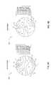
- FIG. 2is a schematic cross sectional view of the rotating substrate support depicted in FIG. 1 ;
- FIG. 3is a detailed view of one embodiment of the interface between the support shaft and the rotor of the rotating substrate support;
- FIGS. 4-5are graphs depicting film thickness non-uniformity for rotating and non-rotating substrates.
- FIGS. 6A-Bare film thickness variation plots for a film formed on a non-rotating and a rotating substrate, respectively.
- One exemplary process chamber suitable for use with a rotating substrate support as described hereinis a low pressure thermal chemical vapor deposition reactor, such as, for example, a SiNgen chamber, available from Applied Materials, Inc., of Santa Clara, Calif. It is contemplated that other process chambers may also benefit from the use of the rotating substrate support described herein.
- FIG. 1illustrates one embodiment of a suitable reactor 100 .
- the reactor 100comprises a base 104 , walls 102 , and a lid 106 (collectively referred to as a chamber body 105 ) that define a reaction chamber, or process volume 108 , in which process gases, precursor gases, or reactant gases are thermally decomposed to form a layer of material on a substrate (not shown).
- At least one port 134is formed in the lid and is coupled to a gas panel 128 that supplies one or more gases to the process volume 108 .
- a gas distribution plate, or showerhead 120is disposed beneath the lid 106 to more uniformly spread the process gases entering through the port 134 throughout the process volume 108 .
- process gases or precursor gases provided by the gas panel 128are introduced into the process volume 108 .
- the process gasis distributed from the port 134 through a plurality of holes (not shown) in the showerhead 120 .
- the showerhead 120uniformly distributes the process gas into the process volume 108 .
- a pumping port 126is formed in the chamber body 105 and is coupled to pumping equipment (not shown) such as valves, pumps, and the like, to selectively maintain the processing pressures within the chamber body 105 as needed.
- pumping equipmentsuch as valves, pumps, and the like
- Other componentssuch as pressure regulators (not shown), sensors (not shown), and the like, may be utilized to monitor the processing pressure within the process volume 108 .
- the chamber body 105is constructed of materials that will enable the chamber to sustain pressures between about 10 to about 350 Torr. In one exemplary embodiment, the chamber body 105 is constructed of an aluminum alloy material.
- the chamber body 105may include passages (not shown) for a temperature controlled fluid to be pumped therethrough to cool the chamber body 105 . Equipped with such temperature controlled fluid passages, the reactor 100 is referred to as a “cold-wall” or a “warm-wall” reactor. Cooling the chamber body 105 prevents corrosion to the material that is used to form the chamber body 105 due to the presence of the reactive species and the high temperature.
- the interior of the chamber body 105may also be lined with a temperature-controlled liner or an insulation liner (not shown) to prevent the undesirable condensation of particles on the interior surfaces of the chamber body 105 .
- the reactor 100further comprises a rotating lift assembly 150 for supporting a substrate within the process volume 108 of the reactor 100 .
- the lift assembly 150includes a substrate support 110 , a shaft 112 , and a substrate support motion assembly 124 .
- the substrate support 110typically houses lift pins 114 and may further include heating elements, electrodes, thermocouples, backside gas grooves, and the like (all not shown for simplicity).
- the substrate support 110includes a heater 136 disposed beneath a substrate receiving pocket 116 .
- the substrate receiving pocket 116is typically approximately the thickness of a substrate.
- the substrate receiving pocket 116may have a plurality of features, such as “bumps,” or stand-offs (not shown), that hold the substrate slightly above the surface of the substrate receiving pocket 116 .
- the heater 136may be utilized to control the temperature of the substrate placed on the substrate support 110 during processing in order to facilitate film formation thereupon.
- the heater 136generally includes one or more resistive coils (not shown) embedded in a conductive body.
- the resistive coilsmay be independently controllable to create heater zones.
- a temperature indicator(not shown) may be provided to monitor the processing temperature inside the chamber body 105 .
- the temperature indicatorcan be a thermocouple (not shown), which is positioned such that it provides data correlating to the temperature at the surface of the substrate support 110 (or at the surface of a substrate supported by the substrate support 110 ).
- the substrate support motion assembly 124moves the substrate support 110 vertically up and down as well as rotationally, as depicted by arrows 131 , 132 .
- the vertical movement of the rotating lift assembly 150facilitates transfer of the substrate into and out of the chamber body 105 and positioning the substrate within the process volume 108 .
- a substrateis typically placed on the substrate support 110 through a port 122 formed in the walls 102 of the chamber body 105 by, for example, a robotic transfer mechanism (not shown).
- the substrate support motion assembly 124lowers the substrate support 110 so that the support surface of the substrate support 110 is below the port 122 .
- the transfer mechanisminserts the substrate through the port 122 to position the substrate above the substrate support 110 .
- the lift pins 114 in the substrate support 110are then raised by raising a contact lift plate 118 that is movably coupled to the base 104 of the reactor 100 .
- the lift pins 114lift the substrate from the transfer mechanism, which is then withdrawn.
- the contact lift plate 118 and lift pins 114are then lowered to place the substrate on the substrate support 110 .
- the port 122is sealed, and the substrate support motion assembly 124 raises the substrate support 110 into processing position.
- the advancementstops when the wafer substrate is a short distance (e.g., 400-900 mils) from the showerhead 120 .
- the substratecan be removed from the chamber by essentially reversing the above steps.
- the rotational movement of the rotating lift assembly 150enables smoothing, or making more uniform, any uneven temperature distribution on the substrate during processing and provides numerous other processing advantages, as detailed below.
- FIG. 2depicts a cross sectional simplified view of one embodiment of the rotating lift assembly 150 .
- the rotating lift assembly 150includes a frame 204 movably coupled to a support 202 disposed beneath the base 104 of the reactor 100 .
- the frame 204may be movably coupled to the support 202 by suitable means, such as linear bearings and the like.
- the framesupports the substrate support 110 via the shaft 112 , which extends through an opening in the base 104 of the reactor 100 .
- a lift mechanism 206is coupled to the frame 204 and moves the frame 204 within the support 202 , thereby providing a range of motion to raise and lower the substrate support 110 within the reactor 100 .
- the lift mechanism 206can be a stepper motor or other suitable mechanism for providing the desired range of motion to the substrate support 110 .
- the frame 204further includes a housing 230 that supports a motor 208 that is coaxially aligned with the shaft 112 and the substrate support 110 .
- the motor 208provides rotary motion to the substrate support 110 via a rotor 210 that is coupled to a shaft 209 of the motor 208 .
- the shaft 209may be hollow to allow cooling water, electrical power, thermocouple signals, and the like to be passed coaxially through the motor 208 .
- a drive 232may be coupled to and provide control over the motor 208 .
- the motor 208typically operates in the range of between about 0 to about 60 rotations per minute (rpm) and has a steady state rotational speed variability of about 1 percent. In one embodiment, the motor 208 rotates in the range of between about 1 and about 15 rpm.
- the motor 208has accurate rotational control and is index capable to within about 1 degree. Such rotational control allows for alignment of a feature, for example, a flat portion of the substrate or a notch formed on the substrate, used to orient the substrate during processing. Additionally, such rotational control allows for the knowledge of the position of any point on a substrate relative to the fixed coordinates of the interior of the reactor 100 .
- the substrate support 110is supported by the motor 208 through the shaft 112 and the rotor 210 , allowing the bearings of the motor 208 to support and align the substrate support 110 .
- the motor 208may be offset from the substrate support 110 , using gears, belts, pulleys, and the like to rotate the substrate support 110 .
- a sensorsuch as an optical sensor, may be provided to prevent rotation of the substrate support 110 when the lift pins 114 are engaged with the lift plate 118 (depicted in FIG. 1 ).
- the optical sensormay be disposed on the outside of the rotating lift assembly 150 and configured to detect when the assembly is at a predetermined height (e.g., a raised processing position or a lowered substrate transfer position).
- the rotor 210typically comprises a process compatible, corrosion-resistant material that reduces friction and wear to facilitate rotation, such as a hardened stainless steel, anodized aluminum, ceramic, and the like.
- the rotor 210may further be polished.
- the rotor 210comprises 17-4PH steel that has been machined, ground, hardened, and polished.
- the seating surfaces at the interface between the shaft 112 and the rotor 210are typically ground to ensure proper alignment of the substrate support 110 relative to a central axis of the motor 208 and the rotor 210 .
- Alignment of the substrate support 110may be accomplished by precision machining. Alternatively or in combination, adjustment mechanisms, such as jack bolts, may also be utilized to assist in the alignment of the substrate support 110 . Such alignment ensures that the central axes of the motor 208 and the substrate support 110 are parallel, thereby reducing rotational wobble of the substrate support 110 .
- the substrate support 110has a surface run-out of between about 0.002 to about 0.003 inches. In one embodiment, the substrate support 110 has a height variation less than about 0.005 inches over a 200 mm diameter support surface. Utilization of a high quality motor 208 with good bearings further assists in reducing substrate support wobble.
- the shaft 112 of the substrate support 110may be coupled to the rotor 210 by any suitable means such as pinning, bolting, screwing, welding, brazing, and the like.
- the shaft 112is removably coupled to the rotor 210 to facilitate quick and easy removal and replacement of the substrate support 110 when desired.
- a plurality of pins 304extend from a base 302 of the shaft 112 .
- An aperture 310is formed in a body 308 of the rotor 210 in a position corresponding to each of the pins 304 such that the shaft may be lowered (as indicated by arrow 318 ) onto the rotor 210 with the pins 304 extending into the apertures 310 .
- a rotatable shaft 312extends partially into the aperture 310 .
- a notch 316is formed in the shaft 312 in a position that allows alignment of the notch 316 with an inner wall of the aperture 310 .
- the pin 304may extend into the aperture 310 unobstructed by the shaft 312 .
- a notch 306 formed in the pin 304is aligned with the shaft 312 .
- the shaft 312may then be rotated, as indicated by arrows 320 , such that the body of the shaft 312 moves into the notch 306 of the pin 304 .
- the body of the shaft 312locks the shaft 112 in position.
- the shaft 312may be eccentric with respect to the notch 306 of the pin 304 to facilitate engaging the pin 304 upon rotation of the shaft 312 .
- the shaft 312may have a cam (not shown) formed thereon that engages the pin 304 when the shaft 312 is rotated.
- an outer end of the shaft 312may have a feature, such as a hex head 314 formed thereon. The hex head 314 is positioned such that a tool may be used to more easily turn the shaft 312 .
- a seal block 212surrounds the rotor 210 and forms a seal therewith. Additionally, a bellows 216 is coupled between the base 104 and the seal block 212 .
- a mounting plate 214may optionally be provided atop the seal block 212 to assist in the alignment of the base of the shaft 112 with the rotor 210 . In the embodiment depicted in FIG. 2 , the bellows 216 is coupled to the mounting plate 214 disposed on top of the seal block 212 .
- the seal block 212may include at least one seal 228 , for example, a lip seal, provided at the interface between the seal block 212 and the rotor 210 .
- the seal 228is typically abrasion resistant and may be formed from polyethylene or other process compatible material. In one embodiment, the seals are formed from polytetrafluoroethylene (PTFE). In the embodiment depicted in FIG. 2 , three seals 228 are disposed between the seal block 212 and the rotor 210 .
- the seal block 212may be allowed to float during installation, and thereby be centered by the pressure of the seals 228 . The seal block 212 may then be bolted, clamped, or otherwise secured upon completion of the installation process.
- One or more grooves, or channels 226may further be provided along the interface between the seal block 212 and the rotor 210 .
- the channel 226may be formed in one or both of the seal block 212 and the rotor 210 and is connected to a pump 224 via lines 225 .
- the pump 224continually maintains the pressure within the channel 226 in a suitable range to maintain the seal between the interior process volume 108 of the reactor 100 and the atmosphere outside of the reactor 100 .
- two channels 226are disposed in the space between the three seals 228 and are coupled to the pump 224 by two lines 225 .
- At least one conduit 242is disposed within the hollow shaft 112 to couple the necessary facilities to the substrate support 110 .
- the conduit 242may contain electrical wires to provide power for the heater 136 , thermocouples and other electric connections to the substrate support.
- Each conduitmay be formed of an insulative material, such as a ceramic, in order to shield and protect the wires.
- a single conduit 242may be used for each electrical connection, thereby isolating each individual wire.
- Other conduits(not shown) may provide cooling gases or fluids where utilized to the substrate support 110 .
- a slip ring 234is provided to run electrical connections from an electrical supply 240 to the substrate support 110 .
- a rotary union 236may be coupled to a coolant supply and return 238 to provide a coolant to the rotating lift assembly for use in cooling the rotor 210 , the base of the shaft 112 , and/or the heater 136 .
- the rotor 210may further comprise air-cooled fins (not shown) to facilitate radiant cooling of the rotor 210 .
- a fan(not shown) may additionally be utilized to increase the air flow rate over the cooling fins. It is contemplated that other cooling mechanisms may be used in combination with the reactor 100 or other processing chamber having the rotating lift assembly 150 . For example, a fan (not shown) may be provided outside the reactor 100 to circulate air and cool the bellows 216 .
- the slip ring 234 and the rotary union 236 or their equivalentsare necessary for methods that rotate the substrate without restriction, it is contemplated that the rotary motion provided by the motor 208 could be reciprocating, rather than continuous rotation in a single direction. As such, the slip ring 234 and the rotary union 236 are considered optional if reciprocating motion is all that is required.
- the electrical and cooling utilitiesmay be provided by flexible conduits (not shown) as well as through the slip ring 234 and the rotary union 236 as depicted in FIG. 2 .
- a purge gas supply line 225is coupled to a purge gas supply 220 to provide a purge gas, such as nitrogen or any other process-inert gas, to an interior volume 218 of the reactor 100 disposed between the bellows 216 and the shaft 112 .
- a purge gassuch as nitrogen or any other process-inert gas
- the purge gas in the interior volume 218prevents the deposition of materials introduced into the reactor 100 onto the interior side of the bellows 216 and/or the shaft 112 .
- a purge gasmay be supplied to the channels 226 from the purge gas supply 220 via a supply line 223 .
- a controller 130is coupled to the chamber body 105 to receive signals from sensors, which indicate the chamber pressure.
- the controller 130can also be coupled to the gas panel 128 to control the flow of gas or gases to the process volume 108 .
- the controller 130can work in conjunction with the pressure regulator or regulators to adjust or to maintain the desired pressure within the process volume 108 .
- the controller 130can control the temperature of the substrate support 110 , and therefore the temperature of a substrate placed thereon.
- the controllercan further be coupled to the rotating lift assembly 150 to control the rotation thereof during processing.
- the controller 130includes a memory which contains instructions in a computer readable format for controlling the gas flows as well as the pressure in the chamber and temperature of the substrate support 110 within parameters set forth above in order to form a layer of material on a substrate in accordance with the present invention.
- the rotating lift assemblycan be employed to minimize the impact of temperature and flow non-uniformity inherent in the processing chamber.
- the impact from hardware manufacturing and installation tolerancese.g., machining and materials tolerances or the installation precision of various parts, will be reduced by the smoothing effect on the flow and temperature inhomogeneities by use of the rotating lift assembly 150 .
- the rotationcreates a substrate environment that time-averages these inhomogeneities, which results in a more uniform film thickness across the substrate.
- the film thickness uniformity improvementapplies for chambers having a gas flow inlet disposed above the wafer, as shown in FIGS. 1-2 , as well as for process chambers having a gas flow inlets arranged to provide a cross-flow, or flow parallel to the substrate diameter.
- FIG. 4depicts a graph 400 of film thickness non-uniformity (axis 402 ), expressed as a percentage, versus a number representative of processing conditions (axis 404 ).
- the data for this chartwas obtained by depositing a silicon nitride film using silane (SiH 4 ) and ammonia (NH 3 ) on a 300 mm bare silicon substrate in a CVD chamber similar to the one described above with respect to FIGS. 1-2 .
- Data points 406represent substrates processed without rotation.
- Data points 408represent substrates processed while rotating the substrate.
- the data points 408reveal lower non-uniformity percentage for substrates processed with substrate rotation, as compared to the data points 406 , for all processing conditions measured (e.g., along axis 404 ).
- FIG. 5depicts a graph 500 of film thickness non-uniformity, expressed as a percentage on axis 502 , for several substrates processed with and without substrate rotation, numbered sequentially on axis 504 .
- the data for this chartwas obtained by depositing a silicon nitride film using bis(tert-butylamino)silane (BTBAS) and ammonia (NH 3 ) on a 300 mm bare silicon substrate in a CVD chamber similar to the one described above with respect to FIGS. 1-2 .
- Data points 506represent substrates processed without rotation.
- Data points 508represent substrates processed while rotating the substrate.
- the data points 508show that rotating the substrate improves, i.e., lowers, the film thickness non-uniformity percentage as compared to substrates processed without rotation (e.g., data points 506 ).
- FIGS. 6A-Bdepict film thickness variation plots across the surface of a substrate for a film deposited on a stationary and a rotating substrate, respectively.
- Plot 610depicted in FIG. 6A
- plot 620shows a greater variation in film thickness across the surface of the substrate for a substrate processed without rotation as compared to plot 620 , depicted in FIG. 6B , which corresponds to a substrate processed while rotating the substrate.
- Another advantage of the rotating lift assembly 150is the increased flow created by the rotation of the substrate, which may further reduce particulate contamination on a substrate. Furthermore, because of the added flow component created by the rotation of the substrate by the rotating lift assembly 150 , lower total flow rates may be used thereby allowing reduction in the inert gases and other dilutants added to the reactant gases to maintain uniform flow or relatively uniform flow within the process chamber. The reduction in the dilutant gases advantageously increases the deposition rate due to the greater concentration of reactant species in the process volume 108 of the reactor 100 .
- the substratemay be in multiples of 360 degrees (including 360 degrees) throughout a particular process cycle.
- the substratemay be rotated multiples of 360 degrees through at least one of a process ramp-up portion, a steady-state portion, and/or a ramp-down portion of a particular process cycle.
- a substrate supported on a substrate support 110may be rotated during a particular process to deposit a uniform seed layer of material. Subsequent to the deposition of the seed layer, bulk deposition over the seed layer may then proceed with or without rotation of the substrate support 110 .
- a substratemay be monitored by appropriate profiling equipment such that the rotation of a substrate supported on the rotating lift assembly 150 may be controlled over the course of multiple process cycles in order to get a desired deposition profile within each process cycle.
- the deposition profilesmay be monitored and adjusted appropriately for each subsequent deposition cycle such that the total deposition thickness profile equals a desired profile (e.g., flat).
- the speed of the rotation of the rotating lift assembly 150may be varied depending upon particular variables that are measured or monitored during the processing of the substrate. For example, process variables known to affect deposition rates, such as temperature or pressure, or a measured or calculated rate of deposition may be utilized to control the speed of rotation of the substrate supported by the substrate support 110 during processing. For example, the substrate may be rotated at slower speeds during slow deposition rate periods and at faster speeds during faster deposition rate periods.
- the substrate supported by the rotating lift assembly 150may be incrementally indexed during processing, rather then uniformly rotated. For example, you can process a substrate in one position for a certain period of time then index the substrate to a new position for a subsequent period of time.
- the substratemay be held in a first orientation for a first period of time, the rotated 180 degrees into a second orientation and processed for a second period of time.
- the substratemay also be indexed in order to align a substrate for removal from the chamber.
- the indexing capabilitymay also be used to retain knowledge of the substrate orientation within the chamber so that process non-uniformities or defects detected on the substrate can be correlated to a specific region of the reactor 100 .
- the rotating lift assemblymay be utilized to provide improved film thickness uniformity in atomic layer deposition (ALD) processes, which pulse gas precursors separately to deposit a film in one atomic layer per cycle.
- ALDatomic layer deposition
- the rotating lift assemblymay be utilized to provide improved film thickness uniformity in ultraviolet (UV) light- or plasma-enhanced thermal deposition processes, which respectively utilize UV light or a plasma to increase chemical reactivity.
- UVultraviolet
Landscapes
- Engineering & Computer Science (AREA)
- Physics & Mathematics (AREA)
- Chemical & Material Sciences (AREA)
- General Physics & Mathematics (AREA)
- Condensed Matter Physics & Semiconductors (AREA)
- Manufacturing & Machinery (AREA)
- Computer Hardware Design (AREA)
- Microelectronics & Electronic Packaging (AREA)
- Power Engineering (AREA)
- Chemical Kinetics & Catalysis (AREA)
- General Chemical & Material Sciences (AREA)
- Materials Engineering (AREA)
- Mechanical Engineering (AREA)
- Metallurgy (AREA)
- Organic Chemistry (AREA)
- Nonlinear Science (AREA)
- Crystallography & Structural Chemistry (AREA)
- Optics & Photonics (AREA)
- Chemical Vapour Deposition (AREA)
- Container, Conveyance, Adherence, Positioning, Of Wafer (AREA)
Abstract
Description
- This application is a divisional application of U.S. application Ser. No. 11/147,938, filed Jun. 8, 2005, which is incorporated herein by reference.
- 1. Field of the Invention
- This application generally relates to the processing of semiconductor substrates and more specifically to the deposition of materials on a semiconductor substrate. More specifically, this invention relates to a rotating substrate support for use in a single-substrate deposition chamber.
- 2. Description of the Related Art
- Integrated circuits comprise multiple layers of materials deposited by various techniques, including chemical vapor deposition. As such, the deposition of materials on a semiconductor substrate via chemical vapor deposition, or CVD, is a critical step in the process of producing integrated circuits. Typical CVD chambers have a heated substrate support for heating a substrate during processing, a gas port for introducing process gases into the chamber, and a pumping port for maintaining the processing pressure within the chamber and to remove excess gases or processing by products. Due to the flow pattern of the gases introduced into the process chamber towards the pumping port, it is difficult to maintain a uniform deposition profile on the substrate. In addition, variance in the emissivity of the internal chamber components leads to non-uniform heat distribution profiles within the chamber and, therefore, on the substrate. Such non uniformities in the heat distribution profile across the surface of the substrate further leads to non uniformities in the deposition of materials on the substrate. This, in turn, leads to further costs incurred in planarizing or otherwise repairing the substrate prior to further processing or possible failure of the integrated circuit all together.
- As such, a need exists for an improved apparatus for uniformly depositing material on a substrate in a CVD chamber.
- A method and apparatus for processing a substrate utilizing a rotating substrate support are disclosed herein. In one embodiment, an apparatus for processing a substrate includes a chamber having a substrate support assembly disposed within the chamber. The substrate support assembly includes a substrate support having a support surface and a heater disposed beneath the support surface. A shaft is coupled to the substrate support and a motor is coupled to the shaft through a rotor to provide rotary movement to the substrate support. A seal block is disposed around the rotor and forms a seal therewith. The seal block has at least one seal and at least one channel disposed along the interface between the seal block and the shaft. A port is coupled to each channel for connecting to a pump. A lift mechanism is coupled to the shaft for raising and lowering the substrate support.
- In another aspect of the invention, various methods of processing a substrate utilizing a rotating substrate support are provided. In one embodiment, a method for processing a substrate in a processing chamber utilizing a rotating substrate support includes the steps of placing a substrate to be processed on the substrate support and rotating the substrate in a multiple of 360 degrees throughout a process cycle. In another embodiment, the deposition rate of a material layer to be formed on the substrate is determined and the rate of rotation of the substrate is controlled in response to the determined deposition rate in order to control a final deposition profile of the material layer. In another embodiment, the speed of rotation of the substrate is controlled in response to a specified variable or variables. The variables may be at least one of temperature, pressure, calculated rate of deposition, or measured rate of deposition. In another embodiment, the substrate may be processed for a first period of time in a first orientation and then indexed to a second orientation and processed for a second period of time.
- So that the manner in which the above recited features of the present invention can be understood in detail, a more particular description of the invention, briefly summarized above, may be had by reference to embodiments, some of which are illustrated in the appended drawings. It is to be noted, however, that the appended drawings illustrate only typical embodiments of this invention and are therefore not to be considered limiting of its scope, for the invention may admit to other equally effective embodiments.
FIG. 1 is a simplified cross sectional view of an exemplary chemical vapor deposition chamber having a rotating substrate support of the present invention;FIG. 2 is a schematic cross sectional view of the rotating substrate support depicted inFIG. 1 ;FIG. 3 is a detailed view of one embodiment of the interface between the support shaft and the rotor of the rotating substrate support;FIGS. 4-5 are graphs depicting film thickness non-uniformity for rotating and non-rotating substrates; andFIGS. 6A-B are film thickness variation plots for a film formed on a non-rotating and a rotating substrate, respectively.- One exemplary process chamber suitable for use with a rotating substrate support as described herein is a low pressure thermal chemical vapor deposition reactor, such as, for example, a SiNgen chamber, available from Applied Materials, Inc., of Santa Clara, Calif. It is contemplated that other process chambers may also benefit from the use of the rotating substrate support described herein.
FIG. 1 illustrates one embodiment of asuitable reactor 100. Thereactor 100 comprises abase 104,walls 102, and a lid106 (collectively referred to as a chamber body105) that define a reaction chamber, or process volume108, in which process gases, precursor gases, or reactant gases are thermally decomposed to form a layer of material on a substrate (not shown).- At least one
port 134 is formed in the lid and is coupled to agas panel 128 that supplies one or more gases to the process volume108. Typically, a gas distribution plate, orshowerhead 120, is disposed beneath thelid 106 to more uniformly spread the process gases entering through theport 134 throughout the process volume108. In one exemplary embodiment, when ready for deposition or processing, process gases or precursor gases provided by thegas panel 128 are introduced into the process volume108. The process gas is distributed from theport 134 through a plurality of holes (not shown) in theshowerhead 120. Theshowerhead 120 uniformly distributes the process gas into the process volume108. - A
pumping port 126 is formed in thechamber body 105 and is coupled to pumping equipment (not shown) such as valves, pumps, and the like, to selectively maintain the processing pressures within thechamber body 105 as needed. Other components, such as pressure regulators (not shown), sensors (not shown), and the like, may be utilized to monitor the processing pressure within the process volume108. Thechamber body 105 is constructed of materials that will enable the chamber to sustain pressures between about 10 to about 350 Torr. In one exemplary embodiment, thechamber body 105 is constructed of an aluminum alloy material. - The
chamber body 105 may include passages (not shown) for a temperature controlled fluid to be pumped therethrough to cool thechamber body 105. Equipped with such temperature controlled fluid passages, thereactor 100 is referred to as a “cold-wall” or a “warm-wall” reactor. Cooling thechamber body 105 prevents corrosion to the material that is used to form thechamber body 105 due to the presence of the reactive species and the high temperature. The interior of thechamber body 105 may also be lined with a temperature-controlled liner or an insulation liner (not shown) to prevent the undesirable condensation of particles on the interior surfaces of thechamber body 105. - The
reactor 100 further comprises a rotatinglift assembly 150 for supporting a substrate within the process volume108 of thereactor 100. Thelift assembly 150 includes asubstrate support 110, ashaft 112, and a substratesupport motion assembly 124. Thesubstrate support 110 typically houseslift pins 114 and may further include heating elements, electrodes, thermocouples, backside gas grooves, and the like (all not shown for simplicity). - In the embodiment depicted in
FIG. 1 , thesubstrate support 110 includes aheater 136 disposed beneath asubstrate receiving pocket 116. Thesubstrate receiving pocket 116 is typically approximately the thickness of a substrate. Thesubstrate receiving pocket 116 may have a plurality of features, such as “bumps,” or stand-offs (not shown), that hold the substrate slightly above the surface of thesubstrate receiving pocket 116. - The
heater 136 may be utilized to control the temperature of the substrate placed on thesubstrate support 110 during processing in order to facilitate film formation thereupon. Theheater 136 generally includes one or more resistive coils (not shown) embedded in a conductive body. The resistive coils may be independently controllable to create heater zones. A temperature indicator (not shown) may be provided to monitor the processing temperature inside thechamber body 105. In one example, the temperature indicator can be a thermocouple (not shown), which is positioned such that it provides data correlating to the temperature at the surface of the substrate support110 (or at the surface of a substrate supported by the substrate support110). - The substrate
support motion assembly 124 moves thesubstrate support 110 vertically up and down as well as rotationally, as depicted byarrows rotating lift assembly 150 facilitates transfer of the substrate into and out of thechamber body 105 and positioning the substrate within the process volume108. - For example, a substrate is typically placed on the
substrate support 110 through aport 122 formed in thewalls 102 of thechamber body 105 by, for example, a robotic transfer mechanism (not shown). The substratesupport motion assembly 124 lowers thesubstrate support 110 so that the support surface of thesubstrate support 110 is below theport 122. The transfer mechanism inserts the substrate through theport 122 to position the substrate above thesubstrate support 110. The lift pins114 in thesubstrate support 110 are then raised by raising acontact lift plate 118 that is movably coupled to thebase 104 of thereactor 100. The lift pins114 lift the substrate from the transfer mechanism, which is then withdrawn. Thecontact lift plate 118 and liftpins 114 are then lowered to place the substrate on thesubstrate support 110. - Once the substrate is loaded and the transfer mechanism retracts, the
port 122 is sealed, and the substratesupport motion assembly 124 raises thesubstrate support 110 into processing position. In one exemplary embodiment, the advancement stops when the wafer substrate is a short distance (e.g., 400-900 mils) from theshowerhead 120. The substrate can be removed from the chamber by essentially reversing the above steps. - The rotational movement of the
rotating lift assembly 150 enables smoothing, or making more uniform, any uneven temperature distribution on the substrate during processing and provides numerous other processing advantages, as detailed below. FIG. 2 depicts a cross sectional simplified view of one embodiment of therotating lift assembly 150. In one embodiment, therotating lift assembly 150 includes aframe 204 movably coupled to asupport 202 disposed beneath thebase 104 of thereactor 100. Theframe 204 may be movably coupled to thesupport 202 by suitable means, such as linear bearings and the like. The frame supports thesubstrate support 110 via theshaft 112, which extends through an opening in thebase 104 of thereactor 100.- A
lift mechanism 206 is coupled to theframe 204 and moves theframe 204 within thesupport 202, thereby providing a range of motion to raise and lower thesubstrate support 110 within thereactor 100. Thelift mechanism 206 can be a stepper motor or other suitable mechanism for providing the desired range of motion to thesubstrate support 110. - The
frame 204 further includes ahousing 230 that supports amotor 208 that is coaxially aligned with theshaft 112 and thesubstrate support 110. Themotor 208 provides rotary motion to thesubstrate support 110 via arotor 210 that is coupled to ashaft 209 of themotor 208. Theshaft 209 may be hollow to allow cooling water, electrical power, thermocouple signals, and the like to be passed coaxially through themotor 208. Adrive 232 may be coupled to and provide control over themotor 208. - The
motor 208 typically operates in the range of between about 0 to about 60 rotations per minute (rpm) and has a steady state rotational speed variability of about 1 percent. In one embodiment, themotor 208 rotates in the range of between about 1 and about 15 rpm. Themotor 208 has accurate rotational control and is index capable to within about 1 degree. Such rotational control allows for alignment of a feature, for example, a flat portion of the substrate or a notch formed on the substrate, used to orient the substrate during processing. Additionally, such rotational control allows for the knowledge of the position of any point on a substrate relative to the fixed coordinates of the interior of thereactor 100. - The
substrate support 110 is supported by themotor 208 through theshaft 112 and therotor 210, allowing the bearings of themotor 208 to support and align thesubstrate support 110. As thesubstrate support 110 is mounted to, and supported by, themotor 208, the number of components is thereby minimized and alignment and coupling problems between multiple sets of bearings may be reduced or eliminated. Alternatively, themotor 208 may be offset from thesubstrate support 110, using gears, belts, pulleys, and the like to rotate thesubstrate support 110. - Optionally, a sensor (not shown), such as an optical sensor, may be provided to prevent rotation of the
substrate support 110 when the lift pins114 are engaged with the lift plate118 (depicted inFIG. 1 ). For example, the optical sensor may be disposed on the outside of therotating lift assembly 150 and configured to detect when the assembly is at a predetermined height (e.g., a raised processing position or a lowered substrate transfer position). - The
rotor 210 typically comprises a process compatible, corrosion-resistant material that reduces friction and wear to facilitate rotation, such as a hardened stainless steel, anodized aluminum, ceramic, and the like. Therotor 210 may further be polished. In one embodiment, therotor 210 comprises 17-4PH steel that has been machined, ground, hardened, and polished. The seating surfaces at the interface between theshaft 112 and therotor 210 are typically ground to ensure proper alignment of thesubstrate support 110 relative to a central axis of themotor 208 and therotor 210. - Alignment of the
substrate support 110 may be accomplished by precision machining. Alternatively or in combination, adjustment mechanisms, such as jack bolts, may also be utilized to assist in the alignment of thesubstrate support 110. Such alignment ensures that the central axes of themotor 208 and thesubstrate support 110 are parallel, thereby reducing rotational wobble of thesubstrate support 110. In one embodiment, thesubstrate support 110 has a surface run-out of between about 0.002 to about 0.003 inches. In one embodiment, thesubstrate support 110 has a height variation less than about 0.005 inches over a 200 mm diameter support surface. Utilization of ahigh quality motor 208 with good bearings further assists in reducing substrate support wobble. - The
shaft 112 of thesubstrate support 110 may be coupled to therotor 210 by any suitable means such as pinning, bolting, screwing, welding, brazing, and the like. In one embodiment, theshaft 112 is removably coupled to therotor 210 to facilitate quick and easy removal and replacement of thesubstrate support 110 when desired. In one embodiment, depicted inFIG. 3 , a plurality of pins304 (one shown inFIG. 3 for clarity) extend from abase 302 of theshaft 112. Anaperture 310 is formed in abody 308 of therotor 210 in a position corresponding to each of thepins 304 such that the shaft may be lowered (as indicated by arrow318) onto therotor 210 with thepins 304 extending into theapertures 310. - A
rotatable shaft 312 extends partially into theaperture 310. Anotch 316 is formed in theshaft 312 in a position that allows alignment of thenotch 316 with an inner wall of theaperture 310. When so aligned, thepin 304 may extend into theaperture 310 unobstructed by theshaft 312. When fully inserted, anotch 306 formed in thepin 304 is aligned with theshaft 312. Theshaft 312 may then be rotated, as indicated byarrows 320, such that the body of theshaft 312 moves into thenotch 306 of thepin 304. Upon rotating theshaft 312, the body of theshaft 312 locks theshaft 112 in position. Theshaft 312 may be eccentric with respect to thenotch 306 of thepin 304 to facilitate engaging thepin 304 upon rotation of theshaft 312. Alternatively or in combination, theshaft 312 may have a cam (not shown) formed thereon that engages thepin 304 when theshaft 312 is rotated. To facilitate rotating theshaft 312, an outer end of theshaft 312 may have a feature, such as ahex head 314 formed thereon. Thehex head 314 is positioned such that a tool may be used to more easily turn theshaft 312. - Returning to
FIG. 2 , in order to maintain the pressure differential between the process volume108 inside thereactor 100 and the atmosphere outside thereactor 100, aseal block 212 surrounds therotor 210 and forms a seal therewith. Additionally, a bellows216 is coupled between the base104 and theseal block 212. A mountingplate 214 may optionally be provided atop theseal block 212 to assist in the alignment of the base of theshaft 112 with therotor 210. In the embodiment depicted inFIG. 2 , thebellows 216 is coupled to the mountingplate 214 disposed on top of theseal block 212. - The
seal block 212 may include at least oneseal 228, for example, a lip seal, provided at the interface between theseal block 212 and therotor 210. Theseal 228 is typically abrasion resistant and may be formed from polyethylene or other process compatible material. In one embodiment, the seals are formed from polytetrafluoroethylene (PTFE). In the embodiment depicted inFIG. 2 , threeseals 228 are disposed between theseal block 212 and therotor 210. To facilitate making theseal block 212 coaxial with therotor 210, theseal block 212 may be allowed to float during installation, and thereby be centered by the pressure of theseals 228. Theseal block 212 may then be bolted, clamped, or otherwise secured upon completion of the installation process. - One or more grooves, or
channels 226, may further be provided along the interface between theseal block 212 and therotor 210. Thechannel 226 may be formed in one or both of theseal block 212 and therotor 210 and is connected to apump 224 vialines 225. Thepump 224 continually maintains the pressure within thechannel 226 in a suitable range to maintain the seal between the interior process volume108 of thereactor 100 and the atmosphere outside of thereactor 100. In the embodiment depicted inFIG. 2 , twochannels 226 are disposed in the space between the threeseals 228 and are coupled to thepump 224 by twolines 225. - At least one
conduit 242 is disposed within thehollow shaft 112 to couple the necessary facilities to thesubstrate support 110. For example, theconduit 242 may contain electrical wires to provide power for theheater 136, thermocouples and other electric connections to the substrate support. Each conduit may be formed of an insulative material, such as a ceramic, in order to shield and protect the wires. In addition, asingle conduit 242 may be used for each electrical connection, thereby isolating each individual wire. Other conduits (not shown) may provide cooling gases or fluids where utilized to thesubstrate support 110. Aslip ring 234 is provided to run electrical connections from anelectrical supply 240 to thesubstrate support 110. - A
rotary union 236 may be coupled to a coolant supply and return238 to provide a coolant to the rotating lift assembly for use in cooling therotor 210, the base of theshaft 112, and/or theheater 136. Alternatively or in combination, therotor 210 may further comprise air-cooled fins (not shown) to facilitate radiant cooling of therotor 210. In embodiments where air-cooled fins are utilized, a fan (not shown) may additionally be utilized to increase the air flow rate over the cooling fins. It is contemplated that other cooling mechanisms may be used in combination with thereactor 100 or other processing chamber having therotating lift assembly 150. For example, a fan (not shown) may be provided outside thereactor 100 to circulate air and cool thebellows 216. - Although the
slip ring 234 and therotary union 236 or their equivalents are necessary for methods that rotate the substrate without restriction, it is contemplated that the rotary motion provided by themotor 208 could be reciprocating, rather than continuous rotation in a single direction. As such, theslip ring 234 and therotary union 236 are considered optional if reciprocating motion is all that is required. For such an embodiment, the electrical and cooling utilities may be provided by flexible conduits (not shown) as well as through theslip ring 234 and therotary union 236 as depicted inFIG. 2 . - A purge
gas supply line 225 is coupled to apurge gas supply 220 to provide a purge gas, such as nitrogen or any other process-inert gas, to aninterior volume 218 of thereactor 100 disposed between thebellows 216 and theshaft 112. The purge gas in theinterior volume 218 prevents the deposition of materials introduced into thereactor 100 onto the interior side of thebellows 216 and/or theshaft 112. Optionally, a purge gas may be supplied to thechannels 226 from thepurge gas supply 220 via asupply line 223. - Returning to
FIG. 1 , in one embodiment, acontroller 130 is coupled to thechamber body 105 to receive signals from sensors, which indicate the chamber pressure. Thecontroller 130 can also be coupled to thegas panel 128 to control the flow of gas or gases to the process volume108. Thecontroller 130 can work in conjunction with the pressure regulator or regulators to adjust or to maintain the desired pressure within the process volume108. Additionally, thecontroller 130 can control the temperature of thesubstrate support 110, and therefore the temperature of a substrate placed thereon. The controller can further be coupled to therotating lift assembly 150 to control the rotation thereof during processing. Thecontroller 130 includes a memory which contains instructions in a computer readable format for controlling the gas flows as well as the pressure in the chamber and temperature of thesubstrate support 110 within parameters set forth above in order to form a layer of material on a substrate in accordance with the present invention. - In operation, the rotating lift assembly can be employed to minimize the impact of temperature and flow non-uniformity inherent in the processing chamber. For example, the impact from hardware manufacturing and installation tolerances, e.g., machining and materials tolerances or the installation precision of various parts, will be reduced by the smoothing effect on the flow and temperature inhomogeneities by use of the
rotating lift assembly 150. The rotation creates a substrate environment that time-averages these inhomogeneities, which results in a more uniform film thickness across the substrate. The film thickness uniformity improvement applies for chambers having a gas flow inlet disposed above the wafer, as shown inFIGS. 1-2 , as well as for process chambers having a gas flow inlets arranged to provide a cross-flow, or flow parallel to the substrate diameter. - For example,
FIG. 4 depicts agraph 400 of film thickness non-uniformity (axis402), expressed as a percentage, versus a number representative of processing conditions (axis404). The data for this chart was obtained by depositing a silicon nitride film using silane (SiH4) and ammonia (NH3) on a 300 mm bare silicon substrate in a CVD chamber similar to the one described above with respect toFIGS. 1-2 . Data points406 represent substrates processed without rotation. Data points408 represent substrates processed while rotating the substrate. The data points408 reveal lower non-uniformity percentage for substrates processed with substrate rotation, as compared to the data points406, for all processing conditions measured (e.g., along axis404). - As another example,
FIG. 5 depicts agraph 500 of film thickness non-uniformity, expressed as a percentage onaxis 502, for several substrates processed with and without substrate rotation, numbered sequentially onaxis 504. The data for this chart was obtained by depositing a silicon nitride film using bis(tert-butylamino)silane (BTBAS) and ammonia (NH3) on a 300 mm bare silicon substrate in a CVD chamber similar to the one described above with respect toFIGS. 1-2 . Data points506 represent substrates processed without rotation. Data points508 represent substrates processed while rotating the substrate. The data points508 show that rotating the substrate improves, i.e., lowers, the film thickness non-uniformity percentage as compared to substrates processed without rotation (e.g., data points506). - As another example,
FIGS. 6A-B depict film thickness variation plots across the surface of a substrate for a film deposited on a stationary and a rotating substrate, respectively. Plot610, depicted inFIG. 6A , shows a greater variation in film thickness across the surface of the substrate for a substrate processed without rotation as compared toplot 620, depicted inFIG. 6B , which corresponds to a substrate processed while rotating the substrate. - Another advantage of the
rotating lift assembly 150 is the increased flow created by the rotation of the substrate, which may further reduce particulate contamination on a substrate. Furthermore, because of the added flow component created by the rotation of the substrate by therotating lift assembly 150, lower total flow rates may be used thereby allowing reduction in the inert gases and other dilutants added to the reactant gases to maintain uniform flow or relatively uniform flow within the process chamber. The reduction in the dilutant gases advantageously increases the deposition rate due to the greater concentration of reactant species in the process volume108 of thereactor 100. - Examples of methods of use of the
rotating lift assembly 150 described above are provided below. In one embodiment, the substrate may be in multiples of 360 degrees (including 360 degrees) throughout a particular process cycle. Alternatively, the substrate may be rotated multiples of 360 degrees through at least one of a process ramp-up portion, a steady-state portion, and/or a ramp-down portion of a particular process cycle. - In another embodiment, a substrate supported on a
substrate support 110 may be rotated during a particular process to deposit a uniform seed layer of material. Subsequent to the deposition of the seed layer, bulk deposition over the seed layer may then proceed with or without rotation of thesubstrate support 110. - A substrate may be monitored by appropriate profiling equipment such that the rotation of a substrate supported on the
rotating lift assembly 150 may be controlled over the course of multiple process cycles in order to get a desired deposition profile within each process cycle. The deposition profiles may be monitored and adjusted appropriately for each subsequent deposition cycle such that the total deposition thickness profile equals a desired profile (e.g., flat). - Furthermore, the speed of the rotation of the
rotating lift assembly 150 may be varied depending upon particular variables that are measured or monitored during the processing of the substrate. For example, process variables known to affect deposition rates, such as temperature or pressure, or a measured or calculated rate of deposition may be utilized to control the speed of rotation of the substrate supported by thesubstrate support 110 during processing. For example, the substrate may be rotated at slower speeds during slow deposition rate periods and at faster speeds during faster deposition rate periods. - In addition, the substrate supported by the
rotating lift assembly 150 may be incrementally indexed during processing, rather then uniformly rotated. For example, you can process a substrate in one position for a certain period of time then index the substrate to a new position for a subsequent period of time. For example, the substrate may be held in a first orientation for a first period of time, the rotated 180 degrees into a second orientation and processed for a second period of time. - The substrate may also be indexed in order to align a substrate for removal from the chamber. The indexing capability may also be used to retain knowledge of the substrate orientation within the chamber so that process non-uniformities or defects detected on the substrate can be correlated to a specific region of the
reactor 100. - While the above methods and apparatus relate to a low temperature chemical vapor deposition chamber, it is contemplated that other chambers and other thin-film deposition processes may be adapted to benefit from the rotating
substrate support 150 described herein. For example, the rotating lift assembly may be utilized to provide improved film thickness uniformity in atomic layer deposition (ALD) processes, which pulse gas precursors separately to deposit a film in one atomic layer per cycle. Alternatively, the rotating lift assembly may be utilized to provide improved film thickness uniformity in ultraviolet (UV) light- or plasma-enhanced thermal deposition processes, which respectively utilize UV light or a plasma to increase chemical reactivity. - While the foregoing is directed to embodiments of the present invention, other and further embodiments of the invention may be devised without departing from the basic scope thereof, and the scope thereof is determined by the claims that follow.
Claims (20)
1. An apparatus for processing a substrate, comprising:
a chamber;
a bellows connected to the chamber;
a substrate support having a heater disposed within the chamber; and
a seal block connecting the substrate support to the bellows.
2. The apparatus ofclaim 1 , wherein the substrate support has a rotor that contacts the seal block.
3. The apparatus ofclaim 2 , further comprising a motor connected to the rotor.
4. The apparatus ofclaim 3 , further comprising a lift mechanism connected to the seal block.
5. The apparatus ofclaim 4 , wherein the bellows has a mounting plate that contacts the seal block.
6. An apparatus for processing a substrate, comprising:
a chamber;
a substrate support having a heater disposed within the chamber and a support pedestal disposed below the heater;
a bellows connected to the chamber and surrounding the support pedestal;
a seal block connecting the support pedestal to the bellows;
a motor connected to the support pedestal; and
a lift mechanism connected to the bellows.
7. The apparatus ofclaim 6 , wherein the bellows has a mounting plate that contacts the seal block.
8. An apparatus for processing a substrate, comprising:
a chamber; and
a substrate support assembly disposed within the chamber, the substrate support assembly comprising:
a substrate support having a support surface;
a heater disposed beneath the support surface;
a shaft coupled to the substrate support;
a motor coupled to the shaft through a rotor to provide rotary movement to the substrate support;
a seal block disposed around the rotor and forming a seal therewith, the seal block having at least one seal and at least one channel disposed along the interface between the seal block and the shaft and a port coupled to each channel for connecting to a pump; and
a lift mechanism coupled to the shaft for raising and lowering the substrate support.
9. The apparatus ofclaim 8 , wherein the motor rotates at a speed of up to about 60 rotations per minute.
10. The apparatus ofclaim 8 , wherein the motor has a steady state rotational variation of within about 1 percent.
11. The apparatus ofclaim 8 , wherein the motor is index capable to less than about 1 degree.
12. The apparatus ofclaim 8 , wherein the seal block further comprises:
a plurality of seals disposed at the interface between the seal block and the shaft, wherein at least one channel is disposed between two of the plurality of seals.
13. The apparatus ofclaim 8 , wherein the seal block further comprises:
three seals and two channels disposed at the interface between the seal block and the shaft, wherein each of the two channels is disposed between two of the three seals.
14. The apparatus ofclaim 8 , further comprising:
a plurality of apertures formed in an upper surface of the rotor; and
a plurality of pins disposed on a bottom of the shaft and extending into the plurality of apertures.
15. The apparatus ofclaim 14 , further comprising:
a notch formed in each pin; and
a rotatable shaft partially protruding into the aperture and having a notch formed therein that, when aligned, allows free movement of the pin into and out of the aperture and, when not aligned prevents the movement of the pin out of the aperture by extending into the notch of the pin.
16. The apparatus ofclaim 8 , further comprising:
three apertures formed in an upper surface of the rotor; and
three pins disposed on a bottom of the shaft, each pin extending into a corresponding one of the three apertures.
17. The apparatus ofclaim 8 , further comprising:
at least one insulative conduit disposed within the shaft and extending from a bottom surface of the substrate support to a bottom portion of the shaft.
18. The apparatus ofclaim 8 , further comprising:
a controller coupled to the substrate support assembly and containing instructions to rotate the substrate support assembly during processing.
19. The apparatus ofclaim 8 , wherein the substrate support is coupled coaxially with the motor, and wherein bearings of the motor support and position the heater.
20. The apparatus ofclaim 8 , wherein the substrate support is driven directly by the motor.
Priority Applications (1)
| Application Number | Priority Date | Filing Date | Title |
|---|---|---|---|
| US12/779,904US20100224130A1 (en) | 2005-06-08 | 2010-05-13 | Rotating substrate support and methods of use |
Applications Claiming Priority (2)
| Application Number | Priority Date | Filing Date | Title |
|---|---|---|---|
| US11/147,938US20060281310A1 (en) | 2005-06-08 | 2005-06-08 | Rotating substrate support and methods of use |
| US12/779,904US20100224130A1 (en) | 2005-06-08 | 2010-05-13 | Rotating substrate support and methods of use |
Related Parent Applications (1)
| Application Number | Title | Priority Date | Filing Date |
|---|---|---|---|
| US11/147,938DivisionUS20060281310A1 (en) | 2005-06-08 | 2005-06-08 | Rotating substrate support and methods of use |
Publications (1)
| Publication Number | Publication Date |
|---|---|
| US20100224130A1true US20100224130A1 (en) | 2010-09-09 |
Family
ID=37398409
Family Applications (3)
| Application Number | Title | Priority Date | Filing Date |
|---|---|---|---|
| US11/147,938AbandonedUS20060281310A1 (en) | 2005-06-08 | 2005-06-08 | Rotating substrate support and methods of use |
| US12/779,904AbandonedUS20100224130A1 (en) | 2005-06-08 | 2010-05-13 | Rotating substrate support and methods of use |
| US13/559,511AbandonedUS20120291709A1 (en) | 2005-06-08 | 2012-07-26 | Rotating substrate support and methods of use |
Family Applications Before (1)
| Application Number | Title | Priority Date | Filing Date |
|---|---|---|---|
| US11/147,938AbandonedUS20060281310A1 (en) | 2005-06-08 | 2005-06-08 | Rotating substrate support and methods of use |
Family Applications After (1)
| Application Number | Title | Priority Date | Filing Date |
|---|---|---|---|
| US13/559,511AbandonedUS20120291709A1 (en) | 2005-06-08 | 2012-07-26 | Rotating substrate support and methods of use |
Country Status (6)
| Country | Link |
|---|---|
| US (3) | US20060281310A1 (en) |
| JP (1) | JP2008544491A (en) |
| KR (6) | KR101038607B1 (en) |
| CN (3) | CN102337521A (en) |
| TW (2) | TWI364810B (en) |
| WO (1) | WO2006132878A2 (en) |
Cited By (299)
| Publication number | Priority date | Publication date | Assignee | Title |
|---|---|---|---|---|
| US20130017503A1 (en)* | 2011-07-13 | 2013-01-17 | De Ridder Chris G M | Wafer processing apparatus with heated, rotating substrate support |
| US20140008349A1 (en)* | 2012-07-03 | 2014-01-09 | Applied Materials, Inc. | Substrate support for substrate backside contamination control |
| US20150090708A1 (en)* | 2012-02-27 | 2015-04-02 | Tokyo Electron Limited | Microwave heating apparatus and processing method |
| US20160020137A1 (en)* | 2014-07-21 | 2016-01-21 | Asm Ip Holding B.V. | Apparatus and method for adjusting a pedestal assembly for a reactor |
| US9593419B2 (en) | 2014-03-12 | 2017-03-14 | Applied Materials, Inc. | Wafer rotation in a semiconductor chamber |
| US10147610B1 (en) | 2017-05-30 | 2018-12-04 | Lam Research Corporation | Substrate pedestal module including metallized ceramic tubes for RF and gas delivery |
| US10847366B2 (en) | 2018-11-16 | 2020-11-24 | Asm Ip Holding B.V. | Methods for depositing a transition metal chalcogenide film on a substrate by a cyclical deposition process |
| US10844484B2 (en) | 2017-09-22 | 2020-11-24 | Asm Ip Holding B.V. | Apparatus for dispensing a vapor phase reactant to a reaction chamber and related methods |
| US10844486B2 (en) | 2009-04-06 | 2020-11-24 | Asm Ip Holding B.V. | Semiconductor processing reactor and components thereof |
| US10851456B2 (en) | 2016-04-21 | 2020-12-01 | Asm Ip Holding B.V. | Deposition of metal borides |
| US10858737B2 (en) | 2014-07-28 | 2020-12-08 | Asm Ip Holding B.V. | Showerhead assembly and components thereof |
| US10867788B2 (en) | 2016-12-28 | 2020-12-15 | Asm Ip Holding B.V. | Method of forming a structure on a substrate |
| US10867786B2 (en) | 2018-03-30 | 2020-12-15 | Asm Ip Holding B.V. | Substrate processing method |
| US10883175B2 (en) | 2018-08-09 | 2021-01-05 | Asm Ip Holding B.V. | Vertical furnace for processing substrates and a liner for use therein |
| US10886123B2 (en) | 2017-06-02 | 2021-01-05 | Asm Ip Holding B.V. | Methods for forming low temperature semiconductor layers and related semiconductor device structures |
| US10892156B2 (en) | 2017-05-08 | 2021-01-12 | Asm Ip Holding B.V. | Methods for forming a silicon nitride film on a substrate and related semiconductor device structures |
| US10910262B2 (en) | 2017-11-16 | 2021-02-02 | Asm Ip Holding B.V. | Method of selectively depositing a capping layer structure on a semiconductor device structure |
| US10914004B2 (en) | 2018-06-29 | 2021-02-09 | Asm Ip Holding B.V. | Thin-film deposition method and manufacturing method of semiconductor device |
| US10923344B2 (en) | 2017-10-30 | 2021-02-16 | Asm Ip Holding B.V. | Methods for forming a semiconductor structure and related semiconductor structures |
| US10928731B2 (en) | 2017-09-21 | 2021-02-23 | Asm Ip Holding B.V. | Method of sequential infiltration synthesis treatment of infiltrateable material and structures and devices formed using same |
| US10934619B2 (en) | 2016-11-15 | 2021-03-02 | Asm Ip Holding B.V. | Gas supply unit and substrate processing apparatus including the gas supply unit |
| US10941490B2 (en) | 2014-10-07 | 2021-03-09 | Asm Ip Holding B.V. | Multiple temperature range susceptor, assembly, reactor and system including the susceptor, and methods of using the same |
| US10943771B2 (en) | 2016-10-26 | 2021-03-09 | Asm Ip Holding B.V. | Methods for thermally calibrating reaction chambers |
| US10950432B2 (en) | 2017-04-25 | 2021-03-16 | Asm Ip Holding B.V. | Method of depositing thin film and method of manufacturing semiconductor device |
| USD913980S1 (en) | 2018-02-01 | 2021-03-23 | Asm Ip Holding B.V. | Gas supply plate for semiconductor manufacturing apparatus |
| US10975470B2 (en) | 2018-02-23 | 2021-04-13 | Asm Ip Holding B.V. | Apparatus for detecting or monitoring for a chemical precursor in a high temperature environment |
| US11001925B2 (en) | 2016-12-19 | 2021-05-11 | Asm Ip Holding B.V. | Substrate processing apparatus |
| US11004977B2 (en) | 2017-07-19 | 2021-05-11 | Asm Ip Holding B.V. | Method for depositing a group IV semiconductor and related semiconductor device structures |
| US11015245B2 (en) | 2014-03-19 | 2021-05-25 | Asm Ip Holding B.V. | Gas-phase reactor and system having exhaust plenum and components thereof |
| US11018002B2 (en) | 2017-07-19 | 2021-05-25 | Asm Ip Holding B.V. | Method for selectively depositing a Group IV semiconductor and related semiconductor device structures |
| US11018047B2 (en) | 2018-01-25 | 2021-05-25 | Asm Ip Holding B.V. | Hybrid lift pin |
| US11022879B2 (en) | 2017-11-24 | 2021-06-01 | Asm Ip Holding B.V. | Method of forming an enhanced unexposed photoresist layer |
| US11024523B2 (en) | 2018-09-11 | 2021-06-01 | Asm Ip Holding B.V. | Substrate processing apparatus and method |
| US11031242B2 (en) | 2018-11-07 | 2021-06-08 | Asm Ip Holding B.V. | Methods for depositing a boron doped silicon germanium film |
| USD922229S1 (en) | 2019-06-05 | 2021-06-15 | Asm Ip Holding B.V. | Device for controlling a temperature of a gas supply unit |
| US11049751B2 (en) | 2018-09-14 | 2021-06-29 | Asm Ip Holding B.V. | Cassette supply system to store and handle cassettes and processing apparatus equipped therewith |
| US11056344B2 (en) | 2017-08-30 | 2021-07-06 | Asm Ip Holding B.V. | Layer forming method |
| US11053591B2 (en) | 2018-08-06 | 2021-07-06 | Asm Ip Holding B.V. | Multi-port gas injection system and reactor system including same |
| US11056567B2 (en) | 2018-05-11 | 2021-07-06 | Asm Ip Holding B.V. | Method of forming a doped metal carbide film on a substrate and related semiconductor device structures |
| US11069510B2 (en) | 2017-08-30 | 2021-07-20 | Asm Ip Holding B.V. | Substrate processing apparatus |
| US11081345B2 (en) | 2018-02-06 | 2021-08-03 | Asm Ip Holding B.V. | Method of post-deposition treatment for silicon oxide film |
| US11088002B2 (en) | 2018-03-29 | 2021-08-10 | Asm Ip Holding B.V. | Substrate rack and a substrate processing system and method |
| US11087997B2 (en) | 2018-10-31 | 2021-08-10 | Asm Ip Holding B.V. | Substrate processing apparatus for processing substrates |
| US11094582B2 (en) | 2016-07-08 | 2021-08-17 | Asm Ip Holding B.V. | Selective deposition method to form air gaps |
| US11094546B2 (en) | 2017-10-05 | 2021-08-17 | Asm Ip Holding B.V. | Method for selectively depositing a metallic film on a substrate |
| US11101370B2 (en) | 2016-05-02 | 2021-08-24 | Asm Ip Holding B.V. | Method of forming a germanium oxynitride film |
| US11107676B2 (en) | 2016-07-28 | 2021-08-31 | Asm Ip Holding B.V. | Method and apparatus for filling a gap |
| US11114283B2 (en) | 2018-03-16 | 2021-09-07 | Asm Ip Holding B.V. | Reactor, system including the reactor, and methods of manufacturing and using same |
| US11114294B2 (en) | 2019-03-08 | 2021-09-07 | Asm Ip Holding B.V. | Structure including SiOC layer and method of forming same |
| USD930782S1 (en) | 2019-08-22 | 2021-09-14 | Asm Ip Holding B.V. | Gas distributor |
| US11127589B2 (en) | 2019-02-01 | 2021-09-21 | Asm Ip Holding B.V. | Method of topology-selective film formation of silicon oxide |
| US11127617B2 (en) | 2017-11-27 | 2021-09-21 | Asm Ip Holding B.V. | Storage device for storing wafer cassettes for use with a batch furnace |
| USD931978S1 (en) | 2019-06-27 | 2021-09-28 | Asm Ip Holding B.V. | Showerhead vacuum transport |
| US11139308B2 (en) | 2015-12-29 | 2021-10-05 | Asm Ip Holding B.V. | Atomic layer deposition of III-V compounds to form V-NAND devices |
| US11139191B2 (en) | 2017-08-09 | 2021-10-05 | Asm Ip Holding B.V. | Storage apparatus for storing cassettes for substrates and processing apparatus equipped therewith |
| US11158513B2 (en) | 2018-12-13 | 2021-10-26 | Asm Ip Holding B.V. | Methods for forming a rhenium-containing film on a substrate by a cyclical deposition process and related semiconductor device structures |
| US11164955B2 (en) | 2017-07-18 | 2021-11-02 | Asm Ip Holding B.V. | Methods for forming a semiconductor device structure and related semiconductor device structures |
| US11171025B2 (en) | 2019-01-22 | 2021-11-09 | Asm Ip Holding B.V. | Substrate processing device |
| USD935572S1 (en) | 2019-05-24 | 2021-11-09 | Asm Ip Holding B.V. | Gas channel plate |
| US11168395B2 (en) | 2018-06-29 | 2021-11-09 | Asm Ip Holding B.V. | Temperature-controlled flange and reactor system including same |
| US11205585B2 (en) | 2016-07-28 | 2021-12-21 | Asm Ip Holding B.V. | Substrate processing apparatus and method of operating the same |
| US11217444B2 (en) | 2018-11-30 | 2022-01-04 | Asm Ip Holding B.V. | Method for forming an ultraviolet radiation responsive metal oxide-containing film |
| US11222772B2 (en) | 2016-12-14 | 2022-01-11 | Asm Ip Holding B.V. | Substrate processing apparatus |
| USD940837S1 (en) | 2019-08-22 | 2022-01-11 | Asm Ip Holding B.V. | Electrode |
| US11227789B2 (en) | 2019-02-20 | 2022-01-18 | Asm Ip Holding B.V. | Method and apparatus for filling a recess formed within a substrate surface |
| US11227782B2 (en) | 2019-07-31 | 2022-01-18 | Asm Ip Holding B.V. | Vertical batch furnace assembly |
| US11233133B2 (en) | 2015-10-21 | 2022-01-25 | Asm Ip Holding B.V. | NbMC layers |
| US11230766B2 (en) | 2018-03-29 | 2022-01-25 | Asm Ip Holding B.V. | Substrate processing apparatus and method |
| US11232963B2 (en) | 2018-10-03 | 2022-01-25 | Asm Ip Holding B.V. | Substrate processing apparatus and method |
| US11242598B2 (en) | 2015-06-26 | 2022-02-08 | Asm Ip Holding B.V. | Structures including metal carbide material, devices including the structures, and methods of forming same |
| US11251035B2 (en) | 2016-12-22 | 2022-02-15 | Asm Ip Holding B.V. | Method of forming a structure on a substrate |
| US11251068B2 (en) | 2018-10-19 | 2022-02-15 | Asm Ip Holding B.V. | Substrate processing apparatus and substrate processing method |
| US11251040B2 (en) | 2019-02-20 | 2022-02-15 | Asm Ip Holding B.V. | Cyclical deposition method including treatment step and apparatus for same |
| USD944946S1 (en) | 2019-06-14 | 2022-03-01 | Asm Ip Holding B.V. | Shower plate |
| US11270899B2 (en) | 2018-06-04 | 2022-03-08 | Asm Ip Holding B.V. | Wafer handling chamber with moisture reduction |
| US11274369B2 (en) | 2018-09-11 | 2022-03-15 | Asm Ip Holding B.V. | Thin film deposition method |
| US11282698B2 (en) | 2019-07-19 | 2022-03-22 | Asm Ip Holding B.V. | Method of forming topology-controlled amorphous carbon polymer film |
| US11286562B2 (en) | 2018-06-08 | 2022-03-29 | Asm Ip Holding B.V. | Gas-phase chemical reactor and method of using same |
| US11289326B2 (en) | 2019-05-07 | 2022-03-29 | Asm Ip Holding B.V. | Method for reforming amorphous carbon polymer film |
| US11286558B2 (en) | 2019-08-23 | 2022-03-29 | Asm Ip Holding B.V. | Methods for depositing a molybdenum nitride film on a surface of a substrate by a cyclical deposition process and related semiconductor device structures including a molybdenum nitride film |
| US11295980B2 (en) | 2017-08-30 | 2022-04-05 | Asm Ip Holding B.V. | Methods for depositing a molybdenum metal film over a dielectric surface of a substrate by a cyclical deposition process and related semiconductor device structures |
| USD947913S1 (en) | 2019-05-17 | 2022-04-05 | Asm Ip Holding B.V. | Susceptor shaft |
| US11296189B2 (en) | 2018-06-21 | 2022-04-05 | Asm Ip Holding B.V. | Method for depositing a phosphorus doped silicon arsenide film and related semiconductor device structures |
| USD948463S1 (en) | 2018-10-24 | 2022-04-12 | Asm Ip Holding B.V. | Susceptor for semiconductor substrate supporting apparatus |
| US11306395B2 (en) | 2017-06-28 | 2022-04-19 | Asm Ip Holding B.V. | Methods for depositing a transition metal nitride film on a substrate by atomic layer deposition and related deposition apparatus |
| USD949319S1 (en) | 2019-08-22 | 2022-04-19 | Asm Ip Holding B.V. | Exhaust duct |
| US11315794B2 (en) | 2019-10-21 | 2022-04-26 | Asm Ip Holding B.V. | Apparatus and methods for selectively etching films |
| US11339476B2 (en) | 2019-10-08 | 2022-05-24 | Asm Ip Holding B.V. | Substrate processing device having connection plates, substrate processing method |
| US11342216B2 (en) | 2019-02-20 | 2022-05-24 | Asm Ip Holding B.V. | Cyclical deposition method and apparatus for filling a recess formed within a substrate surface |
| US11345999B2 (en) | 2019-06-06 | 2022-05-31 | Asm Ip Holding B.V. | Method of using a gas-phase reactor system including analyzing exhausted gas |
| US11355338B2 (en) | 2019-05-10 | 2022-06-07 | Asm Ip Holding B.V. | Method of depositing material onto a surface and structure formed according to the method |
| US11361990B2 (en) | 2018-05-28 | 2022-06-14 | Asm Ip Holding B.V. | Substrate processing method and device manufactured by using the same |
| US11374112B2 (en) | 2017-07-19 | 2022-06-28 | Asm Ip Holding B.V. | Method for depositing a group IV semiconductor and related semiconductor device structures |
| US11378337B2 (en) | 2019-03-28 | 2022-07-05 | Asm Ip Holding B.V. | Door opener and substrate processing apparatus provided therewith |
| US11387106B2 (en) | 2018-02-14 | 2022-07-12 | Asm Ip Holding B.V. | Method for depositing a ruthenium-containing film on a substrate by a cyclical deposition process |
| US11387120B2 (en) | 2017-09-28 | 2022-07-12 | Asm Ip Holding B.V. | Chemical dispensing apparatus and methods for dispensing a chemical to a reaction chamber |
| US11390950B2 (en) | 2017-01-10 | 2022-07-19 | Asm Ip Holding B.V. | Reactor system and method to reduce residue buildup during a film deposition process |
| US11390945B2 (en) | 2019-07-03 | 2022-07-19 | Asm Ip Holding B.V. | Temperature control assembly for substrate processing apparatus and method of using same |
| US11393690B2 (en) | 2018-01-19 | 2022-07-19 | Asm Ip Holding B.V. | Deposition method |
| US11390946B2 (en) | 2019-01-17 | 2022-07-19 | Asm Ip Holding B.V. | Methods of forming a transition metal containing film on a substrate by a cyclical deposition process |
| US11398382B2 (en) | 2018-03-27 | 2022-07-26 | Asm Ip Holding B.V. | Method of forming an electrode on a substrate and a semiconductor device structure including an electrode |
| US11401605B2 (en) | 2019-11-26 | 2022-08-02 | Asm Ip Holding B.V. | Substrate processing apparatus |
| US11410851B2 (en) | 2017-02-15 | 2022-08-09 | Asm Ip Holding B.V. | Methods for forming a metallic film on a substrate by cyclical deposition and related semiconductor device structures |
| US11411088B2 (en) | 2018-11-16 | 2022-08-09 | Asm Ip Holding B.V. | Methods for forming a metal silicate film on a substrate in a reaction chamber and related semiconductor device structures |
| US11414760B2 (en) | 2018-10-08 | 2022-08-16 | Asm Ip Holding B.V. | Substrate support unit, thin film deposition apparatus including the same, and substrate processing apparatus including the same |
| US11417545B2 (en) | 2017-08-08 | 2022-08-16 | Asm Ip Holding B.V. | Radiation shield |
| US11424119B2 (en) | 2019-03-08 | 2022-08-23 | Asm Ip Holding B.V. | Method for selective deposition of silicon nitride layer and structure including selectively-deposited silicon nitride layer |
| US11430674B2 (en) | 2018-08-22 | 2022-08-30 | Asm Ip Holding B.V. | Sensor array, apparatus for dispensing a vapor phase reactant to a reaction chamber and related methods |
| US11430640B2 (en) | 2019-07-30 | 2022-08-30 | Asm Ip Holding B.V. | Substrate processing apparatus |
| US11437241B2 (en) | 2020-04-08 | 2022-09-06 | Asm Ip Holding B.V. | Apparatus and methods for selectively etching silicon oxide films |
| US11443926B2 (en) | 2019-07-30 | 2022-09-13 | Asm Ip Holding B.V. | Substrate processing apparatus |
| US11447861B2 (en) | 2016-12-15 | 2022-09-20 | Asm Ip Holding B.V. | Sequential infiltration synthesis apparatus and a method of forming a patterned structure |
| US11447864B2 (en) | 2019-04-19 | 2022-09-20 | Asm Ip Holding B.V. | Layer forming method and apparatus |
| US11453943B2 (en) | 2016-05-25 | 2022-09-27 | Asm Ip Holding B.V. | Method for forming carbon-containing silicon/metal oxide or nitride film by ALD using silicon precursor and hydrocarbon precursor |
| USD965044S1 (en) | 2019-08-19 | 2022-09-27 | Asm Ip Holding B.V. | Susceptor shaft |
| USD965524S1 (en) | 2019-08-19 | 2022-10-04 | Asm Ip Holding B.V. | Susceptor support |
| US11469098B2 (en) | 2018-05-08 | 2022-10-11 | Asm Ip Holding B.V. | Methods for depositing an oxide film on a substrate by a cyclical deposition process and related device structures |
| US11473195B2 (en) | 2018-03-01 | 2022-10-18 | Asm Ip Holding B.V. | Semiconductor processing apparatus and a method for processing a substrate |
| US11476109B2 (en) | 2019-06-11 | 2022-10-18 | Asm Ip Holding B.V. | Method of forming an electronic structure using reforming gas, system for performing the method, and structure formed using the method |
| US11482418B2 (en) | 2018-02-20 | 2022-10-25 | Asm Ip Holding B.V. | Substrate processing method and apparatus |
| US11482533B2 (en) | 2019-02-20 | 2022-10-25 | Asm Ip Holding B.V. | Apparatus and methods for plug fill deposition in 3-D NAND applications |
| US11482412B2 (en) | 2018-01-19 | 2022-10-25 | Asm Ip Holding B.V. | Method for depositing a gap-fill layer by plasma-assisted deposition |
| US11488854B2 (en) | 2020-03-11 | 2022-11-01 | Asm Ip Holding B.V. | Substrate handling device with adjustable joints |
| US11488819B2 (en) | 2018-12-04 | 2022-11-01 | Asm Ip Holding B.V. | Method of cleaning substrate processing apparatus |
| US11495932B2 (en)* | 2017-06-09 | 2022-11-08 | Applied Materials, Inc. | Slip ring for use in rotatable substrate support |
| US11492703B2 (en) | 2018-06-27 | 2022-11-08 | Asm Ip Holding B.V. | Cyclic deposition methods for forming metal-containing material and films and structures including the metal-containing material |
| US11495459B2 (en) | 2019-09-04 | 2022-11-08 | Asm Ip Holding B.V. | Methods for selective deposition using a sacrificial capping layer |
| US11501956B2 (en) | 2012-10-12 | 2022-11-15 | Asm Ip Holding B.V. | Semiconductor reaction chamber showerhead |
| US11501973B2 (en) | 2018-01-16 | 2022-11-15 | Asm Ip Holding B.V. | Method for depositing a material film on a substrate within a reaction chamber by a cyclical deposition process and related device structures |
| US11499226B2 (en) | 2018-11-02 | 2022-11-15 | Asm Ip Holding B.V. | Substrate supporting unit and a substrate processing device including the same |
| US11499222B2 (en) | 2018-06-27 | 2022-11-15 | Asm Ip Holding B.V. | Cyclic deposition methods for forming metal-containing material and films and structures including the metal-containing material |
| US11501968B2 (en) | 2019-11-15 | 2022-11-15 | Asm Ip Holding B.V. | Method for providing a semiconductor device with silicon filled gaps |
| US11515188B2 (en) | 2019-05-16 | 2022-11-29 | Asm Ip Holding B.V. | Wafer boat handling device, vertical batch furnace and method |
| US11515187B2 (en) | 2020-05-01 | 2022-11-29 | Asm Ip Holding B.V. | Fast FOUP swapping with a FOUP handler |
| US11521851B2 (en) | 2020-02-03 | 2022-12-06 | Asm Ip Holding B.V. | Method of forming structures including a vanadium or indium layer |
| US11527403B2 (en) | 2019-12-19 | 2022-12-13 | Asm Ip Holding B.V. | Methods for filling a gap feature on a substrate surface and related semiconductor structures |
| US11527400B2 (en) | 2019-08-23 | 2022-12-13 | Asm Ip Holding B.V. | Method for depositing silicon oxide film having improved quality by peald using bis(diethylamino)silane |
| US11530876B2 (en) | 2020-04-24 | 2022-12-20 | Asm Ip Holding B.V. | Vertical batch furnace assembly comprising a cooling gas supply |
| US11530483B2 (en) | 2018-06-21 | 2022-12-20 | Asm Ip Holding B.V. | Substrate processing system |
| US11532757B2 (en) | 2016-10-27 | 2022-12-20 | Asm Ip Holding B.V. | Deposition of charge trapping layers |
| US11551912B2 (en) | 2020-01-20 | 2023-01-10 | Asm Ip Holding B.V. | Method of forming thin film and method of modifying surface of thin film |
| US11551925B2 (en) | 2019-04-01 | 2023-01-10 | Asm Ip Holding B.V. | Method for manufacturing a semiconductor device |
| US11557474B2 (en) | 2019-07-29 | 2023-01-17 | Asm Ip Holding B.V. | Methods for selective deposition utilizing n-type dopants and/or alternative dopants to achieve high dopant incorporation |
| USD975665S1 (en) | 2019-05-17 | 2023-01-17 | Asm Ip Holding B.V. | Susceptor shaft |
| US11562901B2 (en) | 2019-09-25 | 2023-01-24 | Asm Ip Holding B.V. | Substrate processing method |
| US11572620B2 (en) | 2018-11-06 | 2023-02-07 | Asm Ip Holding B.V. | Methods for selectively depositing an amorphous silicon film on a substrate |
| US11581186B2 (en) | 2016-12-15 | 2023-02-14 | Asm Ip Holding B.V. | Sequential infiltration synthesis apparatus |
| US11587815B2 (en) | 2019-07-31 | 2023-02-21 | Asm Ip Holding B.V. | Vertical batch furnace assembly |
| US11587814B2 (en) | 2019-07-31 | 2023-02-21 | Asm Ip Holding B.V. | Vertical batch furnace assembly |
| US11587821B2 (en) | 2017-08-08 | 2023-02-21 | Asm Ip Holding B.V. | Substrate lift mechanism and reactor including same |
| US11594600B2 (en) | 2019-11-05 | 2023-02-28 | Asm Ip Holding B.V. | Structures with doped semiconductor layers and methods and systems for forming same |
| USD979506S1 (en) | 2019-08-22 | 2023-02-28 | Asm Ip Holding B.V. | Insulator |
| US11594450B2 (en) | 2019-08-22 | 2023-02-28 | Asm Ip Holding B.V. | Method for forming a structure with a hole |
| USD980813S1 (en) | 2021-05-11 | 2023-03-14 | Asm Ip Holding B.V. | Gas flow control plate for substrate processing apparatus |
| US11605528B2 (en) | 2019-07-09 | 2023-03-14 | Asm Ip Holding B.V. | Plasma device using coaxial waveguide, and substrate treatment method |
| USD980814S1 (en) | 2021-05-11 | 2023-03-14 | Asm Ip Holding B.V. | Gas distributor for substrate processing apparatus |
| US11610774B2 (en) | 2019-10-02 | 2023-03-21 | Asm Ip Holding B.V. | Methods for forming a topographically selective silicon oxide film by a cyclical plasma-enhanced deposition process |
| US11610775B2 (en) | 2016-07-28 | 2023-03-21 | Asm Ip Holding B.V. | Method and apparatus for filling a gap |
| US11615970B2 (en) | 2019-07-17 | 2023-03-28 | Asm Ip Holding B.V. | Radical assist ignition plasma system and method |
| USD981973S1 (en) | 2021-05-11 | 2023-03-28 | Asm Ip Holding B.V. | Reactor wall for substrate processing apparatus |
| US11626316B2 (en) | 2019-11-20 | 2023-04-11 | Asm Ip Holding B.V. | Method of depositing carbon-containing material on a surface of a substrate, structure formed using the method, and system for forming the structure |
| US11626308B2 (en) | 2020-05-13 | 2023-04-11 | Asm Ip Holding B.V. | Laser alignment fixture for a reactor system |
| US11629407B2 (en) | 2019-02-22 | 2023-04-18 | Asm Ip Holding B.V. | Substrate processing apparatus and method for processing substrates |
| US11629406B2 (en) | 2018-03-09 | 2023-04-18 | Asm Ip Holding B.V. | Semiconductor processing apparatus comprising one or more pyrometers for measuring a temperature of a substrate during transfer of the substrate |
| US11637014B2 (en) | 2019-10-17 | 2023-04-25 | Asm Ip Holding B.V. | Methods for selective deposition of doped semiconductor material |
| US11637011B2 (en) | 2019-10-16 | 2023-04-25 | Asm Ip Holding B.V. | Method of topology-selective film formation of silicon oxide |
| US11639548B2 (en) | 2019-08-21 | 2023-05-02 | Asm Ip Holding B.V. | Film-forming material mixed-gas forming device and film forming device |
| US11639811B2 (en) | 2017-11-27 | 2023-05-02 | Asm Ip Holding B.V. | Apparatus including a clean mini environment |
| US11646205B2 (en) | 2019-10-29 | 2023-05-09 | Asm Ip Holding B.V. | Methods of selectively forming n-type doped material on a surface, systems for selectively forming n-type doped material, and structures formed using same |
| US11646197B2 (en) | 2018-07-03 | 2023-05-09 | Asm Ip Holding B.V. | Method for depositing silicon-free carbon-containing film as gap-fill layer by pulse plasma-assisted deposition |
| US11643724B2 (en) | 2019-07-18 | 2023-05-09 | Asm Ip Holding B.V. | Method of forming structures using a neutral beam |
| US11644758B2 (en) | 2020-07-17 | 2023-05-09 | Asm Ip Holding B.V. | Structures and methods for use in photolithography |
| US11646204B2 (en) | 2020-06-24 | 2023-05-09 | Asm Ip Holding B.V. | Method for forming a layer provided with silicon |
| US11646184B2 (en) | 2019-11-29 | 2023-05-09 | Asm Ip Holding B.V. | Substrate processing apparatus |
| US11649546B2 (en) | 2016-07-08 | 2023-05-16 | Asm Ip Holding B.V. | Organic reactants for atomic layer deposition |
| US11658030B2 (en) | 2017-03-29 | 2023-05-23 | Asm Ip Holding B.V. | Method for forming doped metal oxide films on a substrate by cyclical deposition and related semiconductor device structures |
| US11658029B2 (en) | 2018-12-14 | 2023-05-23 | Asm Ip Holding B.V. | Method of forming a device structure using selective deposition of gallium nitride and system for same |
| US11658035B2 (en) | 2020-06-30 | 2023-05-23 | Asm Ip Holding B.V. | Substrate processing method |
| US11664199B2 (en) | 2018-10-19 | 2023-05-30 | Asm Ip Holding B.V. | Substrate processing apparatus and substrate processing method |
| US11664267B2 (en) | 2019-07-10 | 2023-05-30 | Asm Ip Holding B.V. | Substrate support assembly and substrate processing device including the same |
| US11664245B2 (en) | 2019-07-16 | 2023-05-30 | Asm Ip Holding B.V. | Substrate processing device |
| US11674220B2 (en) | 2020-07-20 | 2023-06-13 | Asm Ip Holding B.V. | Method for depositing molybdenum layers using an underlayer |
| US11676812B2 (en) | 2016-02-19 | 2023-06-13 | Asm Ip Holding B.V. | Method for forming silicon nitride film selectively on top/bottom portions |
| US11680839B2 (en) | 2019-08-05 | 2023-06-20 | Asm Ip Holding B.V. | Liquid level sensor for a chemical source vessel |
| USD990534S1 (en) | 2020-09-11 | 2023-06-27 | Asm Ip Holding B.V. | Weighted lift pin |
| US11685991B2 (en) | 2018-02-14 | 2023-06-27 | Asm Ip Holding B.V. | Method for depositing a ruthenium-containing film on a substrate by a cyclical deposition process |
| USD990441S1 (en) | 2021-09-07 | 2023-06-27 | Asm Ip Holding B.V. | Gas flow control plate |
| US11688603B2 (en) | 2019-07-17 | 2023-06-27 | Asm Ip Holding B.V. | Methods of forming silicon germanium structures |
| US11705333B2 (en) | 2020-05-21 | 2023-07-18 | Asm Ip Holding B.V. | Structures including multiple carbon layers and methods of forming and using same |
| TWI810807B (en)* | 2016-10-12 | 2023-08-01 | 美商蘭姆研究公司 | Pad raising mechanism in wafer positioning pedestal for semiconductor processing |
| US11718913B2 (en) | 2018-06-04 | 2023-08-08 | Asm Ip Holding B.V. | Gas distribution system and reactor system including same |
| US11725280B2 (en) | 2020-08-26 | 2023-08-15 | Asm Ip Holding B.V. | Method for forming metal silicon oxide and metal silicon oxynitride layers |
| US11725277B2 (en) | 2011-07-20 | 2023-08-15 | Asm Ip Holding B.V. | Pressure transmitter for a semiconductor processing environment |
| US11735422B2 (en) | 2019-10-10 | 2023-08-22 | Asm Ip Holding B.V. | Method of forming a photoresist underlayer and structure including same |
| US11742198B2 (en) | 2019-03-08 | 2023-08-29 | Asm Ip Holding B.V. | Structure including SiOCN layer and method of forming same |
| US11742189B2 (en) | 2015-03-12 | 2023-08-29 | Asm Ip Holding B.V. | Multi-zone reactor, system including the reactor, and method of using the same |
| US11767589B2 (en) | 2020-05-29 | 2023-09-26 | Asm Ip Holding B.V. | Substrate processing device |
| US11769682B2 (en) | 2017-08-09 | 2023-09-26 | Asm Ip Holding B.V. | Storage apparatus for storing cassettes for substrates and processing apparatus equipped therewith |
| US11776846B2 (en) | 2020-02-07 | 2023-10-03 | Asm Ip Holding B.V. | Methods for depositing gap filling fluids and related systems and devices |
| US11781221B2 (en) | 2019-05-07 | 2023-10-10 | Asm Ip Holding B.V. | Chemical source vessel with dip tube |
| US11781243B2 (en) | 2020-02-17 | 2023-10-10 | Asm Ip Holding B.V. | Method for depositing low temperature phosphorous-doped silicon |
| US11804364B2 (en) | 2020-05-19 | 2023-10-31 | Asm Ip Holding B.V. | Substrate processing apparatus |
| US11802338B2 (en) | 2017-07-26 | 2023-10-31 | Asm Ip Holding B.V. | Chemical treatment, deposition and/or infiltration apparatus and method for using the same |
| US11810788B2 (en) | 2016-11-01 | 2023-11-07 | Asm Ip Holding B.V. | Methods for forming a transition metal niobium nitride film on a substrate by atomic layer deposition and related semiconductor device structures |
| US11814747B2 (en) | 2019-04-24 | 2023-11-14 | Asm Ip Holding B.V. | Gas-phase reactor system-with a reaction chamber, a solid precursor source vessel, a gas distribution system, and a flange assembly |
| US11821078B2 (en) | 2020-04-15 | 2023-11-21 | Asm Ip Holding B.V. | Method for forming precoat film and method for forming silicon-containing film |
| US11823866B2 (en) | 2020-04-02 | 2023-11-21 | Asm Ip Holding B.V. | Thin film forming method |
| US11823876B2 (en) | 2019-09-05 | 2023-11-21 | Asm Ip Holding B.V. | Substrate processing apparatus |
| US11830730B2 (en) | 2017-08-29 | 2023-11-28 | Asm Ip Holding B.V. | Layer forming method and apparatus |
| US11827981B2 (en) | 2020-10-14 | 2023-11-28 | Asm Ip Holding B.V. | Method of depositing material on stepped structure |
| US11828707B2 (en) | 2020-02-04 | 2023-11-28 | Asm Ip Holding B.V. | Method and apparatus for transmittance measurements of large articles |
| US11830738B2 (en) | 2020-04-03 | 2023-11-28 | Asm Ip Holding B.V. | Method for forming barrier layer and method for manufacturing semiconductor device |
| US11840761B2 (en) | 2019-12-04 | 2023-12-12 | Asm Ip Holding B.V. | Substrate processing apparatus |
| US11848200B2 (en) | 2017-05-08 | 2023-12-19 | Asm Ip Holding B.V. | Methods for selectively forming a silicon nitride film on a substrate and related semiconductor device structures |
| US11873557B2 (en) | 2020-10-22 | 2024-01-16 | Asm Ip Holding B.V. | Method of depositing vanadium metal |
| US11876356B2 (en) | 2020-03-11 | 2024-01-16 | Asm Ip Holding B.V. | Lockout tagout assembly and system and method of using same |
| US11887857B2 (en) | 2020-04-24 | 2024-01-30 | Asm Ip Holding B.V. | Methods and systems for depositing a layer comprising vanadium, nitrogen, and a further element |
| US11885013B2 (en) | 2019-12-17 | 2024-01-30 | Asm Ip Holding B.V. | Method of forming vanadium nitride layer and structure including the vanadium nitride layer |
| US11885023B2 (en) | 2018-10-01 | 2024-01-30 | Asm Ip Holding B.V. | Substrate retaining apparatus, system including the apparatus, and method of using same |
| USD1012873S1 (en) | 2020-09-24 | 2024-01-30 | Asm Ip Holding B.V. | Electrode for semiconductor processing apparatus |
| US11885020B2 (en) | 2020-12-22 | 2024-01-30 | Asm Ip Holding B.V. | Transition metal deposition method |
| US11891696B2 (en) | 2020-11-30 | 2024-02-06 | Asm Ip Holding B.V. | Injector configured for arrangement within a reaction chamber of a substrate processing apparatus |
| US11901179B2 (en) | 2020-10-28 | 2024-02-13 | Asm Ip Holding B.V. | Method and device for depositing silicon onto substrates |
| US11898243B2 (en) | 2020-04-24 | 2024-02-13 | Asm Ip Holding B.V. | Method of forming vanadium nitride-containing layer |
| US11915929B2 (en) | 2019-11-26 | 2024-02-27 | Asm Ip Holding B.V. | Methods for selectively forming a target film on a substrate comprising a first dielectric surface and a second metallic surface |
| US11923190B2 (en) | 2018-07-03 | 2024-03-05 | Asm Ip Holding B.V. | Method for depositing silicon-free carbon-containing film as gap-fill layer by pulse plasma-assisted deposition |
| US11923181B2 (en) | 2019-11-29 | 2024-03-05 | Asm Ip Holding B.V. | Substrate processing apparatus for minimizing the effect of a filling gas during substrate processing |
| US11929251B2 (en) | 2019-12-02 | 2024-03-12 | Asm Ip Holding B.V. | Substrate processing apparatus having electrostatic chuck and substrate processing method |
| US11946137B2 (en) | 2020-12-16 | 2024-04-02 | Asm Ip Holding B.V. | Runout and wobble measurement fixtures |
| US11961741B2 (en) | 2020-03-12 | 2024-04-16 | Asm Ip Holding B.V. | Method for fabricating layer structure having target topological profile |
| US11959168B2 (en) | 2020-04-29 | 2024-04-16 | Asm Ip Holding B.V. | Solid source precursor vessel |
| US11967488B2 (en) | 2013-02-01 | 2024-04-23 | Asm Ip Holding B.V. | Method for treatment of deposition reactor |
| USD1023959S1 (en) | 2021-05-11 | 2024-04-23 | Asm Ip Holding B.V. | Electrode for substrate processing apparatus |
| US11976359B2 (en) | 2020-01-06 | 2024-05-07 | Asm Ip Holding B.V. | Gas supply assembly, components thereof, and reactor system including same |
| US11987881B2 (en) | 2020-05-22 | 2024-05-21 | Asm Ip Holding B.V. | Apparatus for depositing thin films using hydrogen peroxide |
| US11986868B2 (en) | 2020-02-28 | 2024-05-21 | Asm Ip Holding B.V. | System dedicated for parts cleaning |
| US11996309B2 (en) | 2019-05-16 | 2024-05-28 | Asm Ip Holding B.V. | Wafer boat handling device, vertical batch furnace and method |
| US11996292B2 (en) | 2019-10-25 | 2024-05-28 | Asm Ip Holding B.V. | Methods for filling a gap feature on a substrate surface and related semiconductor structures |
| US11996289B2 (en) | 2020-04-16 | 2024-05-28 | Asm Ip Holding B.V. | Methods of forming structures including silicon germanium and silicon layers, devices formed using the methods, and systems for performing the methods |
| US11993843B2 (en) | 2017-08-31 | 2024-05-28 | Asm Ip Holding B.V. | Substrate processing apparatus |
| US11993847B2 (en) | 2020-01-08 | 2024-05-28 | Asm Ip Holding B.V. | Injector |
| US12006572B2 (en) | 2019-10-08 | 2024-06-11 | Asm Ip Holding B.V. | Reactor system including a gas distribution assembly for use with activated species and method of using same |
| US12009241B2 (en) | 2019-10-14 | 2024-06-11 | Asm Ip Holding B.V. | Vertical batch furnace assembly with detector to detect cassette |
| US12009224B2 (en) | 2020-09-29 | 2024-06-11 | Asm Ip Holding B.V. | Apparatus and method for etching metal nitrides |
| US12020934B2 (en) | 2020-07-08 | 2024-06-25 | Asm Ip Holding B.V. | Substrate processing method |
| US12027365B2 (en) | 2020-11-24 | 2024-07-02 | Asm Ip Holding B.V. | Methods for filling a gap and related systems and devices |
| US12025484B2 (en) | 2018-05-08 | 2024-07-02 | Asm Ip Holding B.V. | Thin film forming method |
| US12033885B2 (en) | 2020-01-06 | 2024-07-09 | Asm Ip Holding B.V. | Channeled lift pin |
| US12040200B2 (en) | 2017-06-20 | 2024-07-16 | Asm Ip Holding B.V. | Semiconductor processing apparatus and methods for calibrating a semiconductor processing apparatus |
| US12040199B2 (en) | 2018-11-28 | 2024-07-16 | Asm Ip Holding B.V. | Substrate processing apparatus for processing substrates |
| US12040177B2 (en) | 2020-08-18 | 2024-07-16 | Asm Ip Holding B.V. | Methods for forming a laminate film by cyclical plasma-enhanced deposition processes |
| US12051602B2 (en) | 2020-05-04 | 2024-07-30 | Asm Ip Holding B.V. | Substrate processing system for processing substrates with an electronics module located behind a door in a front wall of the substrate processing system |
| US12051567B2 (en) | 2020-10-07 | 2024-07-30 | Asm Ip Holding B.V. | Gas supply unit and substrate processing apparatus including gas supply unit |
| US12057314B2 (en) | 2020-05-15 | 2024-08-06 | Asm Ip Holding B.V. | Methods for silicon germanium uniformity control using multiple precursors |
| US12074022B2 (en) | 2020-08-27 | 2024-08-27 | Asm Ip Holding B.V. | Method and system for forming patterned structures using multiple patterning process |
| US12087586B2 (en) | 2020-04-15 | 2024-09-10 | Asm Ip Holding B.V. | Method of forming chromium nitride layer and structure including the chromium nitride layer |
| US12107005B2 (en) | 2020-10-06 | 2024-10-01 | Asm Ip Holding B.V. | Deposition method and an apparatus for depositing a silicon-containing material |
| US12106944B2 (en) | 2020-06-02 | 2024-10-01 | Asm Ip Holding B.V. | Rotating substrate support |
| US12112940B2 (en) | 2019-07-19 | 2024-10-08 | Asm Ip Holding B.V. | Method of forming topology-controlled amorphous carbon polymer film |
| US12125700B2 (en) | 2020-01-16 | 2024-10-22 | Asm Ip Holding B.V. | Method of forming high aspect ratio features |
| US12131885B2 (en) | 2020-12-22 | 2024-10-29 | Asm Ip Holding B.V. | Plasma treatment device having matching box |
| US12129545B2 (en) | 2020-12-22 | 2024-10-29 | Asm Ip Holding B.V. | Precursor capsule, a vessel and a method |
| US12148609B2 (en) | 2020-09-16 | 2024-11-19 | Asm Ip Holding B.V. | Silicon oxide deposition method |
| US12154824B2 (en) | 2020-08-14 | 2024-11-26 | Asm Ip Holding B.V. | Substrate processing method |
| US12159788B2 (en) | 2020-12-14 | 2024-12-03 | Asm Ip Holding B.V. | Method of forming structures for threshold voltage control |
| US12169361B2 (en) | 2019-07-30 | 2024-12-17 | Asm Ip Holding B.V. | Substrate processing apparatus and method |
| US12173404B2 (en) | 2020-03-17 | 2024-12-24 | Asm Ip Holding B.V. | Method of depositing epitaxial material, structure formed using the method, and system for performing the method |
| US12173402B2 (en) | 2018-02-15 | 2024-12-24 | Asm Ip Holding B.V. | Method of forming a transition metal containing film on a substrate by a cyclical deposition process, a method for supplying a transition metal halide compound to a reaction chamber, and related vapor deposition apparatus |
| US12195852B2 (en) | 2020-11-23 | 2025-01-14 | Asm Ip Holding B.V. | Substrate processing apparatus with an injector |
| US12211742B2 (en) | 2020-09-10 | 2025-01-28 | Asm Ip Holding B.V. | Methods for depositing gap filling fluid |
| US12209308B2 (en) | 2020-11-12 | 2025-01-28 | Asm Ip Holding B.V. | Reactor and related methods |
| US12217946B2 (en) | 2020-10-15 | 2025-02-04 | Asm Ip Holding B.V. | Method of manufacturing semiconductor device, and substrate treatment apparatus using ether-CAT |
| US12218269B2 (en) | 2020-02-13 | 2025-02-04 | Asm Ip Holding B.V. | Substrate processing apparatus including light receiving device and calibration method of light receiving device |
| US12218000B2 (en) | 2020-09-25 | 2025-02-04 | Asm Ip Holding B.V. | Semiconductor processing method |
| US12217954B2 (en) | 2020-08-25 | 2025-02-04 | Asm Ip Holding B.V. | Method of cleaning a surface |
| USD1060598S1 (en) | 2021-12-03 | 2025-02-04 | Asm Ip Holding B.V. | Split showerhead cover |
| US12221357B2 (en) | 2020-04-24 | 2025-02-11 | Asm Ip Holding B.V. | Methods and apparatus for stabilizing vanadium compounds |
| US12230531B2 (en) | 2018-04-09 | 2025-02-18 | Asm Ip Holding B.V. | Substrate supporting apparatus, substrate processing apparatus including the same, and substrate processing method |
| US12241158B2 (en) | 2020-07-20 | 2025-03-04 | Asm Ip Holding B.V. | Method for forming structures including transition metal layers |
| US12243747B2 (en) | 2020-04-24 | 2025-03-04 | Asm Ip Holding B.V. | Methods of forming structures including vanadium boride and vanadium phosphide layers |
| US12243742B2 (en) | 2020-04-21 | 2025-03-04 | Asm Ip Holding B.V. | Method for processing a substrate |
| US12240760B2 (en) | 2016-03-18 | 2025-03-04 | Asm Ip Holding B.V. | Aligned carbon nanotubes |
| US12243757B2 (en) | 2020-05-21 | 2025-03-04 | Asm Ip Holding B.V. | Flange and apparatus for processing substrates |
| US12247286B2 (en) | 2019-08-09 | 2025-03-11 | Asm Ip Holding B.V. | Heater assembly including cooling apparatus and method of using same |
| US12255053B2 (en) | 2020-12-10 | 2025-03-18 | Asm Ip Holding B.V. | Methods and systems for depositing a layer |
| US12252785B2 (en) | 2019-06-10 | 2025-03-18 | Asm Ip Holding B.V. | Method for cleaning quartz epitaxial chambers |
| US12266524B2 (en) | 2020-06-16 | 2025-04-01 | Asm Ip Holding B.V. | Method for depositing boron containing silicon germanium layers |
| US12272527B2 (en) | 2018-05-09 | 2025-04-08 | Asm Ip Holding B.V. | Apparatus for use with hydrogen radicals and method of using same |
| US12278129B2 (en) | 2020-03-04 | 2025-04-15 | Asm Ip Holding B.V. | Alignment fixture for a reactor system |
| US12276023B2 (en) | 2017-08-04 | 2025-04-15 | Asm Ip Holding B.V. | Showerhead assembly for distributing a gas within a reaction chamber |
| US12288710B2 (en) | 2020-12-18 | 2025-04-29 | Asm Ip Holding B.V. | Wafer processing apparatus with a rotatable table |
| US12322591B2 (en) | 2020-07-27 | 2025-06-03 | Asm Ip Holding B.V. | Thin film deposition process |
| US12378665B2 (en) | 2018-10-26 | 2025-08-05 | Asm Ip Holding B.V. | High temperature coatings for a preclean and etch apparatus and related methods |
| US12406846B2 (en) | 2020-05-26 | 2025-09-02 | Asm Ip Holding B.V. | Method for depositing boron and gallium containing silicon germanium layers |
| US12410515B2 (en) | 2020-01-29 | 2025-09-09 | Asm Ip Holding B.V. | Contaminant trap system for a reactor system |
| US12428726B2 (en) | 2019-10-08 | 2025-09-30 | Asm Ip Holding B.V. | Gas injection system and reactor system including same |
| US12431354B2 (en) | 2020-07-01 | 2025-09-30 | Asm Ip Holding B.V. | Silicon nitride and silicon oxide deposition methods using fluorine inhibitor |
| US12431334B2 (en) | 2020-02-13 | 2025-09-30 | Asm Ip Holding B.V. | Gas distribution assembly |
| US12442082B2 (en) | 2021-05-04 | 2025-10-14 | Asm Ip Holding B.V. | Reactor system comprising a tuning circuit |
Families Citing this family (46)
| Publication number | Priority date | Publication date | Assignee | Title |
|---|---|---|---|---|
| CN100358098C (en) | 2005-08-05 | 2007-12-26 | 中微半导体设备(上海)有限公司 | Semiconductor arts piece processing device |
| JP2007324369A (en)* | 2006-06-01 | 2007-12-13 | Sekisui Chem Co Ltd | Substrate circumference treating apparatus |
| CN101140344A (en)* | 2006-09-08 | 2008-03-12 | 鸿富锦精密工业(深圳)有限公司 | Dispensing method |
| US7378618B1 (en)* | 2006-12-14 | 2008-05-27 | Applied Materials, Inc. | Rapid conductive cooling using a secondary process plane |
| WO2008103758A1 (en)* | 2007-02-20 | 2008-08-28 | Tech M3, Inc. | Wear resistant coating for brake disks with unique surface appearance and methods for coating |
| TWI349720B (en)* | 2007-05-30 | 2011-10-01 | Ind Tech Res Inst | A power-delivery mechanism and apparatus of plasma-enhanced chemical vapor deposition using the same |
| KR101046520B1 (en)* | 2007-09-07 | 2011-07-04 | 어플라이드 머티어리얼스, 인코포레이티드 | Source gas flow path control in pecvd system to control a by-product film deposition on inside chamber |
| US20090194026A1 (en)* | 2008-01-31 | 2009-08-06 | Burrows Brian H | Processing system for fabricating compound nitride semiconductor devices |
| US20090194024A1 (en)* | 2008-01-31 | 2009-08-06 | Applied Materials, Inc. | Cvd apparatus |
| US20100075488A1 (en)* | 2008-09-19 | 2010-03-25 | Applied Materials, Inc. | Cvd reactor with multiple processing levels and dual-axis motorized lift mechanism |
| US8425977B2 (en) | 2008-09-29 | 2013-04-23 | Applied Materials, Inc. | Substrate processing chamber with off-center gas delivery funnel |
| US20100101730A1 (en)* | 2008-10-29 | 2010-04-29 | Jusung Engineering Co., Ltd. | Substrate processing apparatus |
| SG10201401671SA (en)* | 2009-04-21 | 2014-07-30 | Applied Materials Inc | Cvd apparatus for improved film thickness non-uniformity and particle performance |
| CN102498557A (en)* | 2009-08-05 | 2012-06-13 | 应用材料公司 | Chemical Vapor Deposition Equipment |
| US8274017B2 (en)* | 2009-12-18 | 2012-09-25 | Applied Materials, Inc. | Multifunctional heater/chiller pedestal for wide range wafer temperature control |
| EP2850221B1 (en)* | 2012-05-18 | 2022-07-06 | Veeco Instruments Inc. | Rotating disk reactor with ferrofluid seal for chemical vapor deposition |
| TW201437421A (en)* | 2013-02-20 | 2014-10-01 | Applied Materials Inc | Apparatus and methods for carousel atomic layer deposition |
| TW201437423A (en)* | 2013-02-21 | 2014-10-01 | Applied Materials Inc | Apparatus and methods for injector to substrate gap control |
| US10351956B2 (en) | 2013-03-14 | 2019-07-16 | Applied Materials, Inc. | Integrated two-axis lift-rotation motor center pedestal in multi-wafer carousel ALD |
| KR102261013B1 (en) | 2013-03-14 | 2021-06-03 | 어플라이드 머티어리얼스, 인코포레이티드 | Temperature measurement in multi-zone heater |
| US20140263275A1 (en)* | 2013-03-15 | 2014-09-18 | Applied Materials, Inc. | Rotation enabled multifunctional heater-chiller pedestal |
| CN103343334A (en)* | 2013-07-18 | 2013-10-09 | 湖南顶立科技有限公司 | Vapor deposition method |
| TWI665753B (en)* | 2014-06-05 | 2019-07-11 | 美商應用材料股份有限公司 | Integrated two-axis lift-rotation motor center pedestal in multi-wafer carousel ald |
| JP6356516B2 (en) | 2014-07-22 | 2018-07-11 | 東芝メモリ株式会社 | Plasma processing apparatus and plasma processing method |
| US9490116B2 (en)* | 2015-01-09 | 2016-11-08 | Applied Materials, Inc. | Gate stack materials for semiconductor applications for lithographic overlay improvement |
| US10081861B2 (en)* | 2015-04-08 | 2018-09-25 | Varian Semiconductor Equipment Associates, Inc. | Selective processing of a workpiece |
| TWI677046B (en)* | 2015-04-23 | 2019-11-11 | 美商應用材料股份有限公司 | External substrate rotation in a semiconductor processing system |
| JP6054470B2 (en)* | 2015-05-26 | 2016-12-27 | 株式会社日本製鋼所 | Atomic layer growth equipment |
| JP2017228597A (en)* | 2016-06-20 | 2017-12-28 | 三星電子株式会社Samsung Electronics Co.,Ltd. | Deposition equipment |
| JP6650841B2 (en)* | 2016-06-27 | 2020-02-19 | 東京エレクトロン株式会社 | Substrate lifting mechanism, substrate mounting table and substrate processing device |
| RU2638870C1 (en)* | 2016-07-05 | 2017-12-18 | Акционерное общество "Концерн "Центральный научно-исследовательский институт "Электроприбор" | Method for manufacturing rotor of electrostatic gyroscope and device for implementation of this method |
| DE102017100507B4 (en)* | 2017-01-12 | 2021-11-25 | Ald Vacuum Technologies Gmbh | Device and method for coating workpieces |
| CN109423630A (en)* | 2017-09-04 | 2019-03-05 | 台湾积体电路制造股份有限公司 | Lifting device, chemical vapor deposition device and method |
| CN107761077B (en)* | 2017-10-20 | 2019-12-03 | 京东方科技集团股份有限公司 | A kind of film plating process, device and PECVD device |
| US11133200B2 (en) | 2017-10-30 | 2021-09-28 | Taiwan Semiconductor Manufacturing Co., Ltd. | Substrate vapor drying apparatus and method |
| US20190131585A1 (en)* | 2017-11-01 | 2019-05-02 | Shenzhen China Star Optoelectronics Semiconductor Display Technology Co., Ltd. | Apparatus of pecvd and manufacturing method of oled panel |
| CN110047790B (en)* | 2018-01-15 | 2021-10-15 | 北京北方华创微电子装备有限公司 | Biaxial mechanism and semiconductor processing apparatus |
| US11251067B2 (en)* | 2019-04-26 | 2022-02-15 | Applied Materials, Inc. | Pedestal lift for semiconductor processing chambers |
| WO2020257141A1 (en)* | 2019-06-20 | 2020-12-24 | Lam Research Corporation | Use of rotation to correct for azimuthal non-uniformities in semiconductor substrate processing |
| CN111364026B (en)* | 2020-05-27 | 2020-08-14 | 上海陛通半导体能源科技股份有限公司 | Reciprocating rotary CVD equipment and application method |
| US11501957B2 (en) | 2020-09-03 | 2022-11-15 | Applied Materials, Inc. | Pedestal support design for precise chamber matching and process control |
| WO2022048241A1 (en)* | 2020-09-07 | 2022-03-10 | 江苏鲁汶仪器有限公司 | Ion beam etching machine and lifting and rotating platform device thereof |
| CN113774360B (en)* | 2021-11-11 | 2022-02-11 | 陛通半导体设备(苏州)有限公司 | Chemical vapor deposition equipment capable of reciprocating, rotating and lifting |
| US20230162955A1 (en)* | 2021-11-24 | 2023-05-25 | Applied Materials, Inc. | Electrostatic chuck with detachable shaft |
| CN114695245B (en)* | 2022-03-29 | 2023-02-07 | 苏州矽行半导体技术有限公司 | Lifting shaft and wafer carrying platform |
| US20240427255A1 (en)* | 2023-06-20 | 2024-12-26 | Applied Materials, Inc. | Rotary Substrate Support Having an Actuator for Aligning a Substrate |
Citations (35)
| Publication number | Priority date | Publication date | Assignee | Title |
|---|---|---|---|---|
| US4438154A (en)* | 1982-04-28 | 1984-03-20 | Stanley Electric Co., Ltd. | Method of fabricating an amorphous silicon film |
| US4591417A (en)* | 1983-12-27 | 1986-05-27 | Ford Motor Company | Tandem deposition of cermets |
| US4676994A (en)* | 1983-06-15 | 1987-06-30 | The Boc Group, Inc. | Adherent ceramic coatings |
| US4770121A (en)* | 1982-11-27 | 1988-09-13 | Toshiba Kikai Kabushiki Kaisha | Semiconductor vapor phase growing apparatus |
| US4897284A (en)* | 1987-03-27 | 1990-01-30 | Canon Kabushiki Kaisha | Process for forming a deposited film on each of a plurality of substrates by way of microwave plasma chemical vapor deposition method |
| US4923584A (en)* | 1988-10-31 | 1990-05-08 | Eaton Corporation | Sealing apparatus for a vacuum processing system |
| US4929840A (en)* | 1989-02-28 | 1990-05-29 | Eaton Corporation | Wafer rotation control for an ion implanter |
| US5407755A (en)* | 1993-06-14 | 1995-04-18 | Eastman Kodak Company | Multilayer magnetooptic recording media |
| US5421893A (en)* | 1993-02-26 | 1995-06-06 | Applied Materials, Inc. | Susceptor drive and wafer displacement mechanism |
| US5576059A (en)* | 1993-01-13 | 1996-11-19 | Applied Materials, Inc. | Depositing polysilicon films having improved uniformity and apparatus therefor |
| US5628829A (en)* | 1994-06-03 | 1997-05-13 | Materials Research Corporation | Method and apparatus for low temperature deposition of CVD and PECVD films |
| US5695832A (en)* | 1993-07-07 | 1997-12-09 | Sanyo Electric Co., Ltd. | Method of forming a hard-carbon-film-coated substrate |
| US5710407A (en)* | 1993-01-21 | 1998-01-20 | Moore Epitaxial, Inc. | Rapid thermal processing apparatus for processing semiconductor wafers |
| US5747113A (en)* | 1996-07-29 | 1998-05-05 | Tsai; Charles Su-Chang | Method of chemical vapor deposition for producing layer variation by planetary susceptor rotation |
| US5772773A (en)* | 1996-05-20 | 1998-06-30 | Applied Materials, Inc. | Co-axial motorized wafer lift |
| US5814365A (en)* | 1997-08-15 | 1998-09-29 | Micro C Technologies, Inc. | Reactor and method of processing a semiconductor substate |
| US5866204A (en)* | 1996-07-23 | 1999-02-02 | The Governors Of The University Of Alberta | Method of depositing shadow sculpted thin films |
| US5928427A (en)* | 1994-12-16 | 1999-07-27 | Hwang; Chul-Ju | Apparatus for low pressure chemical vapor deposition |
| US6264752B1 (en)* | 1998-03-13 | 2001-07-24 | Gary L. Curtis | Reactor for processing a microelectronic workpiece |
| US6287635B1 (en)* | 1997-08-11 | 2001-09-11 | Torrex Equipment Corp. | High rate silicon deposition method at low pressures |
| US20010052392A1 (en)* | 1998-02-25 | 2001-12-20 | Masahiko Nakamura | Multichamber substrate processing apparatus |
| US6419802B1 (en)* | 2001-03-16 | 2002-07-16 | David Alan Baldwin | System and method for controlling deposition thickness by synchronously varying a sputtering rate of a target with respect to a position of a rotating substrate |
| US20020106826A1 (en)* | 2001-02-07 | 2002-08-08 | Vadim Boguslavskiy | Susceptorless reactor for growing epitaxial layers on wafers by chemical vapor deposition |
| US6457557B1 (en)* | 2000-06-27 | 2002-10-01 | Leslie Anderson | Tool for retrieving a ladder from an elevated position |
| US20020139307A1 (en)* | 2000-12-04 | 2002-10-03 | Applied Materials, Inc. | Cooling gas delivery system for a rotatable semiconductor substrate support assembly |
| US6475557B1 (en)* | 1998-08-26 | 2002-11-05 | Nippon Telegraph And Telephone Corporation | Method for manufacturing optical filter |
| US6592679B2 (en)* | 2001-07-13 | 2003-07-15 | Asyst Technologies, Inc. | Clean method for vacuum holding of substrates |
| US6616816B2 (en)* | 2000-08-01 | 2003-09-09 | Anelva Corporation | Substrate processing device and method |
| US6645303B2 (en)* | 1996-11-14 | 2003-11-11 | Applied Materials, Inc. | Heater/lift assembly for high temperature processing chamber |
| US20040013808A1 (en)* | 2002-07-16 | 2004-01-22 | Hanson Kyle M. | Apparatus and method for thermally controlled processing of microelectronic workpieces |
| US6699004B1 (en)* | 2000-03-08 | 2004-03-02 | Advanced Micro Devices, Inc. | Wafer rotation in wafer handling devices |
| US20040057343A1 (en)* | 2002-09-18 | 2004-03-25 | Matsushita Electric Industrial Co., Ltd. | Magnetic recording medium, method for producing the same and magnetic recording/reproducing apparatus |
| US6723214B2 (en)* | 1998-10-29 | 2004-04-20 | Applied Materials, Inc. | Apparatus for improved power coupling through a workpiece in a semiconductor wafer processing system |
| US20040082171A1 (en)* | 2002-09-17 | 2004-04-29 | Shin Cheol Ho | ALD apparatus and ALD method for manufacturing semiconductor device |
| US6812157B1 (en)* | 1999-06-24 | 2004-11-02 | Prasad Narhar Gadgil | Apparatus for atomic layer chemical vapor deposition |
Family Cites Families (14)
| Publication number | Priority date | Publication date | Assignee | Title |
|---|---|---|---|---|
| US4902531A (en)* | 1986-10-30 | 1990-02-20 | Nihon Shinku Gijutsu Kabushiki Kaisha | Vacuum processing method and apparatus |
| US5850089A (en)* | 1992-03-13 | 1998-12-15 | American Research Corporation Of Virginia | Modulated-structure of PZT/PT ferroelectric thin films for non-volatile random access memories |
| US5580421A (en)* | 1994-06-14 | 1996-12-03 | Fsi International | Apparatus for surface conditioning |
| KR100225916B1 (en)* | 1994-12-16 | 1999-10-15 | 황철주 | Low pressure chemical vapor deposition system applying plasma |
| US6120609A (en)* | 1996-10-25 | 2000-09-19 | Applied Materials, Inc. | Self-aligning lift mechanism |
| US6321680B2 (en)* | 1997-08-11 | 2001-11-27 | Torrex Equipment Corporation | Vertical plasma enhanced process apparatus and method |
| US6352593B1 (en)* | 1997-08-11 | 2002-03-05 | Torrex Equipment Corp. | Mini-batch process chamber |
| WO2001020663A1 (en)* | 1999-09-13 | 2001-03-22 | Tokyo Electron Limited | Vacuum processing device |
| JP2002050809A (en)* | 2000-08-01 | 2002-02-15 | Anelva Corp | Substrate processing apparatus and method |
| JP3579690B2 (en)* | 2000-09-01 | 2004-10-20 | 独立行政法人 科学技術振興機構 | A method and apparatus for producing a composite oxide thin film and a composite oxide thin film produced by the method. |
| US6645344B2 (en)* | 2001-05-18 | 2003-11-11 | Tokyo Electron Limited | Universal backplane assembly and methods |
| US20030159652A1 (en)* | 2002-02-25 | 2003-08-28 | United Microelectronics Corp. | Heating injection apparatus for vapor liquid delivery system |
| US6905737B2 (en)* | 2002-10-11 | 2005-06-14 | Applied Materials, Inc. | Method of delivering activated species for rapid cyclical deposition |
| JP3972126B2 (en)* | 2004-05-28 | 2007-09-05 | 独立行政法人産業技術総合研究所 | Ultraviolet generation source, ultraviolet irradiation processing apparatus and semiconductor manufacturing apparatus |
- 2005
- 2005-06-08USUS11/147,938patent/US20060281310A1/ennot_activeAbandoned
- 2006
- 2006-05-31KRKR1020107003773Apatent/KR101038607B1/enactiveActive
- 2006-05-31JPJP2008515759Apatent/JP2008544491A/ennot_activeWithdrawn
- 2006-05-31KRKR1020107003774Apatent/KR20100035180A/ennot_activeCeased
- 2006-05-31KRKR1020077030109Apatent/KR100979329B1/enactiveActive
- 2006-05-31KRKR1020117010620Apatent/KR101343025B1/enactiveActive
- 2006-05-31CNCN2011103376840Apatent/CN102337521A/enactivePending
- 2006-05-31KRKR1020147009579Apatent/KR20140061516A/ennot_activeCeased
- 2006-05-31WOPCT/US2006/021077patent/WO2006132878A2/enactiveApplication Filing
- 2006-05-31CNCN2006800205024Apatent/CN101194040B/enactiveActive
- 2006-05-31CNCN201210041686.XApatent/CN102560433B/enactiveActive
- 2006-05-31KRKR1020137022545Apatent/KR20130114255A/ennot_activeCeased
- 2006-06-08TWTW095120429Apatent/TWI364810B/enactive
- 2006-06-08TWTW100130755Apatent/TW201203430A/enunknown
- 2010
- 2010-05-13USUS12/779,904patent/US20100224130A1/ennot_activeAbandoned
- 2012
- 2012-07-26USUS13/559,511patent/US20120291709A1/ennot_activeAbandoned
Patent Citations (38)
| Publication number | Priority date | Publication date | Assignee | Title |
|---|---|---|---|---|
| US4438154A (en)* | 1982-04-28 | 1984-03-20 | Stanley Electric Co., Ltd. | Method of fabricating an amorphous silicon film |
| US4770121A (en)* | 1982-11-27 | 1988-09-13 | Toshiba Kikai Kabushiki Kaisha | Semiconductor vapor phase growing apparatus |
| US4676994A (en)* | 1983-06-15 | 1987-06-30 | The Boc Group, Inc. | Adherent ceramic coatings |
| US4591417A (en)* | 1983-12-27 | 1986-05-27 | Ford Motor Company | Tandem deposition of cermets |
| US4897284A (en)* | 1987-03-27 | 1990-01-30 | Canon Kabushiki Kaisha | Process for forming a deposited film on each of a plurality of substrates by way of microwave plasma chemical vapor deposition method |
| US4923584A (en)* | 1988-10-31 | 1990-05-08 | Eaton Corporation | Sealing apparatus for a vacuum processing system |
| US4929840A (en)* | 1989-02-28 | 1990-05-29 | Eaton Corporation | Wafer rotation control for an ion implanter |
| US5576059A (en)* | 1993-01-13 | 1996-11-19 | Applied Materials, Inc. | Depositing polysilicon films having improved uniformity and apparatus therefor |
| US6402850B1 (en)* | 1993-01-13 | 2002-06-11 | Applied Materials, Inc. | Depositing polysilicon films having improved uniformity and apparatus therefor |
| US5710407A (en)* | 1993-01-21 | 1998-01-20 | Moore Epitaxial, Inc. | Rapid thermal processing apparatus for processing semiconductor wafers |
| US5421893A (en)* | 1993-02-26 | 1995-06-06 | Applied Materials, Inc. | Susceptor drive and wafer displacement mechanism |
| US5407755A (en)* | 1993-06-14 | 1995-04-18 | Eastman Kodak Company | Multilayer magnetooptic recording media |
| US5695832A (en)* | 1993-07-07 | 1997-12-09 | Sanyo Electric Co., Ltd. | Method of forming a hard-carbon-film-coated substrate |
| US5628829A (en)* | 1994-06-03 | 1997-05-13 | Materials Research Corporation | Method and apparatus for low temperature deposition of CVD and PECVD films |
| US6190460B1 (en)* | 1994-12-16 | 2001-02-20 | Chul-Ju Hwang | Apparatus for low pressure chemical vapor depostion |
| US5928427A (en)* | 1994-12-16 | 1999-07-27 | Hwang; Chul-Ju | Apparatus for low pressure chemical vapor deposition |
| US5772773A (en)* | 1996-05-20 | 1998-06-30 | Applied Materials, Inc. | Co-axial motorized wafer lift |
| US5866204A (en)* | 1996-07-23 | 1999-02-02 | The Governors Of The University Of Alberta | Method of depositing shadow sculpted thin films |
| US5747113A (en)* | 1996-07-29 | 1998-05-05 | Tsai; Charles Su-Chang | Method of chemical vapor deposition for producing layer variation by planetary susceptor rotation |
| US6645303B2 (en)* | 1996-11-14 | 2003-11-11 | Applied Materials, Inc. | Heater/lift assembly for high temperature processing chamber |
| US6287635B1 (en)* | 1997-08-11 | 2001-09-11 | Torrex Equipment Corp. | High rate silicon deposition method at low pressures |
| US5814365A (en)* | 1997-08-15 | 1998-09-29 | Micro C Technologies, Inc. | Reactor and method of processing a semiconductor substate |
| US20010052392A1 (en)* | 1998-02-25 | 2001-12-20 | Masahiko Nakamura | Multichamber substrate processing apparatus |
| US6264752B1 (en)* | 1998-03-13 | 2001-07-24 | Gary L. Curtis | Reactor for processing a microelectronic workpiece |
| US6475557B1 (en)* | 1998-08-26 | 2002-11-05 | Nippon Telegraph And Telephone Corporation | Method for manufacturing optical filter |
| US6723214B2 (en)* | 1998-10-29 | 2004-04-20 | Applied Materials, Inc. | Apparatus for improved power coupling through a workpiece in a semiconductor wafer processing system |
| US6812157B1 (en)* | 1999-06-24 | 2004-11-02 | Prasad Narhar Gadgil | Apparatus for atomic layer chemical vapor deposition |
| US6699004B1 (en)* | 2000-03-08 | 2004-03-02 | Advanced Micro Devices, Inc. | Wafer rotation in wafer handling devices |
| US6457557B1 (en)* | 2000-06-27 | 2002-10-01 | Leslie Anderson | Tool for retrieving a ladder from an elevated position |
| US6616816B2 (en)* | 2000-08-01 | 2003-09-09 | Anelva Corporation | Substrate processing device and method |
| US20020139307A1 (en)* | 2000-12-04 | 2002-10-03 | Applied Materials, Inc. | Cooling gas delivery system for a rotatable semiconductor substrate support assembly |
| US20020106826A1 (en)* | 2001-02-07 | 2002-08-08 | Vadim Boguslavskiy | Susceptorless reactor for growing epitaxial layers on wafers by chemical vapor deposition |
| US6419802B1 (en)* | 2001-03-16 | 2002-07-16 | David Alan Baldwin | System and method for controlling deposition thickness by synchronously varying a sputtering rate of a target with respect to a position of a rotating substrate |
| US6592679B2 (en)* | 2001-07-13 | 2003-07-15 | Asyst Technologies, Inc. | Clean method for vacuum holding of substrates |
| US20040013808A1 (en)* | 2002-07-16 | 2004-01-22 | Hanson Kyle M. | Apparatus and method for thermally controlled processing of microelectronic workpieces |
| US20040082171A1 (en)* | 2002-09-17 | 2004-04-29 | Shin Cheol Ho | ALD apparatus and ALD method for manufacturing semiconductor device |
| US7435445B2 (en)* | 2002-09-17 | 2008-10-14 | Moohan Co., Ltd. | Method for manufacturing semiconductor device |
| US20040057343A1 (en)* | 2002-09-18 | 2004-03-25 | Matsushita Electric Industrial Co., Ltd. | Magnetic recording medium, method for producing the same and magnetic recording/reproducing apparatus |
Cited By (365)
| Publication number | Priority date | Publication date | Assignee | Title |
|---|---|---|---|---|
| US10844486B2 (en) | 2009-04-06 | 2020-11-24 | Asm Ip Holding B.V. | Semiconductor processing reactor and components thereof |
| US9018567B2 (en)* | 2011-07-13 | 2015-04-28 | Asm International N.V. | Wafer processing apparatus with heated, rotating substrate support |
| US20130017503A1 (en)* | 2011-07-13 | 2013-01-17 | De Ridder Chris G M | Wafer processing apparatus with heated, rotating substrate support |
| US11725277B2 (en) | 2011-07-20 | 2023-08-15 | Asm Ip Holding B.V. | Pressure transmitter for a semiconductor processing environment |
| US20150090708A1 (en)* | 2012-02-27 | 2015-04-02 | Tokyo Electron Limited | Microwave heating apparatus and processing method |
| US20140008349A1 (en)* | 2012-07-03 | 2014-01-09 | Applied Materials, Inc. | Substrate support for substrate backside contamination control |
| US9490150B2 (en)* | 2012-07-03 | 2016-11-08 | Applied Materials, Inc. | Substrate support for substrate backside contamination control |
| US11501956B2 (en) | 2012-10-12 | 2022-11-15 | Asm Ip Holding B.V. | Semiconductor reaction chamber showerhead |
| US11967488B2 (en) | 2013-02-01 | 2024-04-23 | Asm Ip Holding B.V. | Method for treatment of deposition reactor |
| US9593419B2 (en) | 2014-03-12 | 2017-03-14 | Applied Materials, Inc. | Wafer rotation in a semiconductor chamber |
| US9922819B2 (en) | 2014-03-12 | 2018-03-20 | Applied Materials, Inc. | Wafer rotation in a semiconductor chamber |
| US11015245B2 (en) | 2014-03-19 | 2021-05-25 | Asm Ip Holding B.V. | Gas-phase reactor and system having exhaust plenum and components thereof |
| US20160020137A1 (en)* | 2014-07-21 | 2016-01-21 | Asm Ip Holding B.V. | Apparatus and method for adjusting a pedestal assembly for a reactor |
| US11417563B2 (en) | 2014-07-21 | 2022-08-16 | Asm America, Inc. | Apparatus and method for adjusting a pedestal assembly for a reactor |
| US11088015B2 (en) | 2014-07-21 | 2021-08-10 | Asm Ip Holding B.V. | Apparatus for adjusting a pedestal assembly for a reactor |
| US10186450B2 (en)* | 2014-07-21 | 2019-01-22 | Asm Ip Holding B.V. | Apparatus and method for adjusting a pedestal assembly for a reactor |
| US10858737B2 (en) | 2014-07-28 | 2020-12-08 | Asm Ip Holding B.V. | Showerhead assembly and components thereof |
| US11795545B2 (en) | 2014-10-07 | 2023-10-24 | Asm Ip Holding B.V. | Multiple temperature range susceptor, assembly, reactor and system including the susceptor, and methods of using the same |
| US10941490B2 (en) | 2014-10-07 | 2021-03-09 | Asm Ip Holding B.V. | Multiple temperature range susceptor, assembly, reactor and system including the susceptor, and methods of using the same |
| US11742189B2 (en) | 2015-03-12 | 2023-08-29 | Asm Ip Holding B.V. | Multi-zone reactor, system including the reactor, and method of using the same |
| US11242598B2 (en) | 2015-06-26 | 2022-02-08 | Asm Ip Holding B.V. | Structures including metal carbide material, devices including the structures, and methods of forming same |
| US11233133B2 (en) | 2015-10-21 | 2022-01-25 | Asm Ip Holding B.V. | NbMC layers |
| US11956977B2 (en) | 2015-12-29 | 2024-04-09 | Asm Ip Holding B.V. | Atomic layer deposition of III-V compounds to form V-NAND devices |
| US11139308B2 (en) | 2015-12-29 | 2021-10-05 | Asm Ip Holding B.V. | Atomic layer deposition of III-V compounds to form V-NAND devices |
| US11676812B2 (en) | 2016-02-19 | 2023-06-13 | Asm Ip Holding B.V. | Method for forming silicon nitride film selectively on top/bottom portions |
| US12240760B2 (en) | 2016-03-18 | 2025-03-04 | Asm Ip Holding B.V. | Aligned carbon nanotubes |
| US10851456B2 (en) | 2016-04-21 | 2020-12-01 | Asm Ip Holding B.V. | Deposition of metal borides |
| US11101370B2 (en) | 2016-05-02 | 2021-08-24 | Asm Ip Holding B.V. | Method of forming a germanium oxynitride film |
| US11453943B2 (en) | 2016-05-25 | 2022-09-27 | Asm Ip Holding B.V. | Method for forming carbon-containing silicon/metal oxide or nitride film by ALD using silicon precursor and hydrocarbon precursor |
| US11649546B2 (en) | 2016-07-08 | 2023-05-16 | Asm Ip Holding B.V. | Organic reactants for atomic layer deposition |
| US11749562B2 (en) | 2016-07-08 | 2023-09-05 | Asm Ip Holding B.V. | Selective deposition method to form air gaps |
| US11094582B2 (en) | 2016-07-08 | 2021-08-17 | Asm Ip Holding B.V. | Selective deposition method to form air gaps |
| US11610775B2 (en) | 2016-07-28 | 2023-03-21 | Asm Ip Holding B.V. | Method and apparatus for filling a gap |
| US11107676B2 (en) | 2016-07-28 | 2021-08-31 | Asm Ip Holding B.V. | Method and apparatus for filling a gap |
| US11205585B2 (en) | 2016-07-28 | 2021-12-21 | Asm Ip Holding B.V. | Substrate processing apparatus and method of operating the same |
| US11694892B2 (en) | 2016-07-28 | 2023-07-04 | Asm Ip Holding B.V. | Method and apparatus for filling a gap |
| TWI810807B (en)* | 2016-10-12 | 2023-08-01 | 美商蘭姆研究公司 | Pad raising mechanism in wafer positioning pedestal for semiconductor processing |
| US10943771B2 (en) | 2016-10-26 | 2021-03-09 | Asm Ip Holding B.V. | Methods for thermally calibrating reaction chambers |
| US11532757B2 (en) | 2016-10-27 | 2022-12-20 | Asm Ip Holding B.V. | Deposition of charge trapping layers |
| US11810788B2 (en) | 2016-11-01 | 2023-11-07 | Asm Ip Holding B.V. | Methods for forming a transition metal niobium nitride film on a substrate by atomic layer deposition and related semiconductor device structures |
| US11396702B2 (en) | 2016-11-15 | 2022-07-26 | Asm Ip Holding B.V. | Gas supply unit and substrate processing apparatus including the gas supply unit |
| US10934619B2 (en) | 2016-11-15 | 2021-03-02 | Asm Ip Holding B.V. | Gas supply unit and substrate processing apparatus including the gas supply unit |
| US11222772B2 (en) | 2016-12-14 | 2022-01-11 | Asm Ip Holding B.V. | Substrate processing apparatus |
| US11970766B2 (en) | 2016-12-15 | 2024-04-30 | Asm Ip Holding B.V. | Sequential infiltration synthesis apparatus |
| US12000042B2 (en) | 2016-12-15 | 2024-06-04 | Asm Ip Holding B.V. | Sequential infiltration synthesis apparatus and a method of forming a patterned structure |
| US11851755B2 (en) | 2016-12-15 | 2023-12-26 | Asm Ip Holding B.V. | Sequential infiltration synthesis apparatus and a method of forming a patterned structure |
| US11581186B2 (en) | 2016-12-15 | 2023-02-14 | Asm Ip Holding B.V. | Sequential infiltration synthesis apparatus |
| US11447861B2 (en) | 2016-12-15 | 2022-09-20 | Asm Ip Holding B.V. | Sequential infiltration synthesis apparatus and a method of forming a patterned structure |
| US11001925B2 (en) | 2016-12-19 | 2021-05-11 | Asm Ip Holding B.V. | Substrate processing apparatus |
| US11251035B2 (en) | 2016-12-22 | 2022-02-15 | Asm Ip Holding B.V. | Method of forming a structure on a substrate |
| US10867788B2 (en) | 2016-12-28 | 2020-12-15 | Asm Ip Holding B.V. | Method of forming a structure on a substrate |
| US12043899B2 (en) | 2017-01-10 | 2024-07-23 | Asm Ip Holding B.V. | Reactor system and method to reduce residue buildup during a film deposition process |
| US11390950B2 (en) | 2017-01-10 | 2022-07-19 | Asm Ip Holding B.V. | Reactor system and method to reduce residue buildup during a film deposition process |
| US12106965B2 (en) | 2017-02-15 | 2024-10-01 | Asm Ip Holding B.V. | Methods for forming a metallic film on a substrate by cyclical deposition and related semiconductor device structures |
| US11410851B2 (en) | 2017-02-15 | 2022-08-09 | Asm Ip Holding B.V. | Methods for forming a metallic film on a substrate by cyclical deposition and related semiconductor device structures |
| US11658030B2 (en) | 2017-03-29 | 2023-05-23 | Asm Ip Holding B.V. | Method for forming doped metal oxide films on a substrate by cyclical deposition and related semiconductor device structures |
| US10950432B2 (en) | 2017-04-25 | 2021-03-16 | Asm Ip Holding B.V. | Method of depositing thin film and method of manufacturing semiconductor device |
| US10892156B2 (en) | 2017-05-08 | 2021-01-12 | Asm Ip Holding B.V. | Methods for forming a silicon nitride film on a substrate and related semiconductor device structures |
| US11848200B2 (en) | 2017-05-08 | 2023-12-19 | Asm Ip Holding B.V. | Methods for selectively forming a silicon nitride film on a substrate and related semiconductor device structures |
| US10964545B2 (en) | 2017-05-30 | 2021-03-30 | Lam Research Corporation | Apparatus including metallized-ceramic tubes for radio-frequency and gas delivery |
| US10431467B2 (en) | 2017-05-30 | 2019-10-01 | Lam Research Corporation | Module including metallized ceramic tubes for RF and gas delivery |
| US10147610B1 (en) | 2017-05-30 | 2018-12-04 | Lam Research Corporation | Substrate pedestal module including metallized ceramic tubes for RF and gas delivery |
| US10886123B2 (en) | 2017-06-02 | 2021-01-05 | Asm Ip Holding B.V. | Methods for forming low temperature semiconductor layers and related semiconductor device structures |
| US11495932B2 (en)* | 2017-06-09 | 2022-11-08 | Applied Materials, Inc. | Slip ring for use in rotatable substrate support |
| US12040200B2 (en) | 2017-06-20 | 2024-07-16 | Asm Ip Holding B.V. | Semiconductor processing apparatus and methods for calibrating a semiconductor processing apparatus |
| US11306395B2 (en) | 2017-06-28 | 2022-04-19 | Asm Ip Holding B.V. | Methods for depositing a transition metal nitride film on a substrate by atomic layer deposition and related deposition apparatus |
| US11976361B2 (en) | 2017-06-28 | 2024-05-07 | Asm Ip Holding B.V. | Methods for depositing a transition metal nitride film on a substrate by atomic layer deposition and related deposition apparatus |
| US11164955B2 (en) | 2017-07-18 | 2021-11-02 | Asm Ip Holding B.V. | Methods for forming a semiconductor device structure and related semiconductor device structures |
| US11695054B2 (en) | 2017-07-18 | 2023-07-04 | Asm Ip Holding B.V. | Methods for forming a semiconductor device structure and related semiconductor device structures |
| US11374112B2 (en) | 2017-07-19 | 2022-06-28 | Asm Ip Holding B.V. | Method for depositing a group IV semiconductor and related semiconductor device structures |
| US12363960B2 (en) | 2017-07-19 | 2025-07-15 | Asm Ip Holding B.V. | Method for depositing a Group IV semiconductor and related semiconductor device structures |
| US11018002B2 (en) | 2017-07-19 | 2021-05-25 | Asm Ip Holding B.V. | Method for selectively depositing a Group IV semiconductor and related semiconductor device structures |
| US11004977B2 (en) | 2017-07-19 | 2021-05-11 | Asm Ip Holding B.V. | Method for depositing a group IV semiconductor and related semiconductor device structures |
| US11802338B2 (en) | 2017-07-26 | 2023-10-31 | Asm Ip Holding B.V. | Chemical treatment, deposition and/or infiltration apparatus and method for using the same |
| US12276023B2 (en) | 2017-08-04 | 2025-04-15 | Asm Ip Holding B.V. | Showerhead assembly for distributing a gas within a reaction chamber |
| US11587821B2 (en) | 2017-08-08 | 2023-02-21 | Asm Ip Holding B.V. | Substrate lift mechanism and reactor including same |
| US11417545B2 (en) | 2017-08-08 | 2022-08-16 | Asm Ip Holding B.V. | Radiation shield |
| US11139191B2 (en) | 2017-08-09 | 2021-10-05 | Asm Ip Holding B.V. | Storage apparatus for storing cassettes for substrates and processing apparatus equipped therewith |
| US11769682B2 (en) | 2017-08-09 | 2023-09-26 | Asm Ip Holding B.V. | Storage apparatus for storing cassettes for substrates and processing apparatus equipped therewith |
| US11830730B2 (en) | 2017-08-29 | 2023-11-28 | Asm Ip Holding B.V. | Layer forming method and apparatus |
| US11295980B2 (en) | 2017-08-30 | 2022-04-05 | Asm Ip Holding B.V. | Methods for depositing a molybdenum metal film over a dielectric surface of a substrate by a cyclical deposition process and related semiconductor device structures |
| US11069510B2 (en) | 2017-08-30 | 2021-07-20 | Asm Ip Holding B.V. | Substrate processing apparatus |
| US11581220B2 (en) | 2017-08-30 | 2023-02-14 | Asm Ip Holding B.V. | Methods for depositing a molybdenum metal film over a dielectric surface of a substrate by a cyclical deposition process and related semiconductor device structures |
| US11056344B2 (en) | 2017-08-30 | 2021-07-06 | Asm Ip Holding B.V. | Layer forming method |
| US11993843B2 (en) | 2017-08-31 | 2024-05-28 | Asm Ip Holding B.V. | Substrate processing apparatus |
| US10928731B2 (en) | 2017-09-21 | 2021-02-23 | Asm Ip Holding B.V. | Method of sequential infiltration synthesis treatment of infiltrateable material and structures and devices formed using same |
| US10844484B2 (en) | 2017-09-22 | 2020-11-24 | Asm Ip Holding B.V. | Apparatus for dispensing a vapor phase reactant to a reaction chamber and related methods |
| US11387120B2 (en) | 2017-09-28 | 2022-07-12 | Asm Ip Holding B.V. | Chemical dispensing apparatus and methods for dispensing a chemical to a reaction chamber |
| US11094546B2 (en) | 2017-10-05 | 2021-08-17 | Asm Ip Holding B.V. | Method for selectively depositing a metallic film on a substrate |
| US12033861B2 (en) | 2017-10-05 | 2024-07-09 | Asm Ip Holding B.V. | Method for selectively depositing a metallic film on a substrate |
| US10923344B2 (en) | 2017-10-30 | 2021-02-16 | Asm Ip Holding B.V. | Methods for forming a semiconductor structure and related semiconductor structures |
| US12040184B2 (en) | 2017-10-30 | 2024-07-16 | Asm Ip Holding B.V. | Methods for forming a semiconductor structure and related semiconductor structures |
| US10910262B2 (en) | 2017-11-16 | 2021-02-02 | Asm Ip Holding B.V. | Method of selectively depositing a capping layer structure on a semiconductor device structure |
| US11022879B2 (en) | 2017-11-24 | 2021-06-01 | Asm Ip Holding B.V. | Method of forming an enhanced unexposed photoresist layer |
| US11682572B2 (en) | 2017-11-27 | 2023-06-20 | Asm Ip Holdings B.V. | Storage device for storing wafer cassettes for use with a batch furnace |
| US11127617B2 (en) | 2017-11-27 | 2021-09-21 | Asm Ip Holding B.V. | Storage device for storing wafer cassettes for use with a batch furnace |
| US11639811B2 (en) | 2017-11-27 | 2023-05-02 | Asm Ip Holding B.V. | Apparatus including a clean mini environment |
| US11501973B2 (en) | 2018-01-16 | 2022-11-15 | Asm Ip Holding B.V. | Method for depositing a material film on a substrate within a reaction chamber by a cyclical deposition process and related device structures |
| US12119228B2 (en) | 2018-01-19 | 2024-10-15 | Asm Ip Holding B.V. | Deposition method |
| US11972944B2 (en) | 2018-01-19 | 2024-04-30 | Asm Ip Holding B.V. | Method for depositing a gap-fill layer by plasma-assisted deposition |
| US11482412B2 (en) | 2018-01-19 | 2022-10-25 | Asm Ip Holding B.V. | Method for depositing a gap-fill layer by plasma-assisted deposition |
| US11393690B2 (en) | 2018-01-19 | 2022-07-19 | Asm Ip Holding B.V. | Deposition method |
| US11018047B2 (en) | 2018-01-25 | 2021-05-25 | Asm Ip Holding B.V. | Hybrid lift pin |
| USD913980S1 (en) | 2018-02-01 | 2021-03-23 | Asm Ip Holding B.V. | Gas supply plate for semiconductor manufacturing apparatus |
| US11081345B2 (en) | 2018-02-06 | 2021-08-03 | Asm Ip Holding B.V. | Method of post-deposition treatment for silicon oxide film |
| US11735414B2 (en) | 2018-02-06 | 2023-08-22 | Asm Ip Holding B.V. | Method of post-deposition treatment for silicon oxide film |
| US11685991B2 (en) | 2018-02-14 | 2023-06-27 | Asm Ip Holding B.V. | Method for depositing a ruthenium-containing film on a substrate by a cyclical deposition process |
| US11387106B2 (en) | 2018-02-14 | 2022-07-12 | Asm Ip Holding B.V. | Method for depositing a ruthenium-containing film on a substrate by a cyclical deposition process |
| US12173402B2 (en) | 2018-02-15 | 2024-12-24 | Asm Ip Holding B.V. | Method of forming a transition metal containing film on a substrate by a cyclical deposition process, a method for supplying a transition metal halide compound to a reaction chamber, and related vapor deposition apparatus |
| US11482418B2 (en) | 2018-02-20 | 2022-10-25 | Asm Ip Holding B.V. | Substrate processing method and apparatus |
| US10975470B2 (en) | 2018-02-23 | 2021-04-13 | Asm Ip Holding B.V. | Apparatus for detecting or monitoring for a chemical precursor in a high temperature environment |
| US11939673B2 (en) | 2018-02-23 | 2024-03-26 | Asm Ip Holding B.V. | Apparatus for detecting or monitoring for a chemical precursor in a high temperature environment |
| US11473195B2 (en) | 2018-03-01 | 2022-10-18 | Asm Ip Holding B.V. | Semiconductor processing apparatus and a method for processing a substrate |
| US11629406B2 (en) | 2018-03-09 | 2023-04-18 | Asm Ip Holding B.V. | Semiconductor processing apparatus comprising one or more pyrometers for measuring a temperature of a substrate during transfer of the substrate |
| US11114283B2 (en) | 2018-03-16 | 2021-09-07 | Asm Ip Holding B.V. | Reactor, system including the reactor, and methods of manufacturing and using same |
| US11398382B2 (en) | 2018-03-27 | 2022-07-26 | Asm Ip Holding B.V. | Method of forming an electrode on a substrate and a semiconductor device structure including an electrode |
| US12020938B2 (en) | 2018-03-27 | 2024-06-25 | Asm Ip Holding B.V. | Method of forming an electrode on a substrate and a semiconductor device structure including an electrode |
| US11230766B2 (en) | 2018-03-29 | 2022-01-25 | Asm Ip Holding B.V. | Substrate processing apparatus and method |
| US11088002B2 (en) | 2018-03-29 | 2021-08-10 | Asm Ip Holding B.V. | Substrate rack and a substrate processing system and method |
| US10867786B2 (en) | 2018-03-30 | 2020-12-15 | Asm Ip Holding B.V. | Substrate processing method |
| US12230531B2 (en) | 2018-04-09 | 2025-02-18 | Asm Ip Holding B.V. | Substrate supporting apparatus, substrate processing apparatus including the same, and substrate processing method |
| US11469098B2 (en) | 2018-05-08 | 2022-10-11 | Asm Ip Holding B.V. | Methods for depositing an oxide film on a substrate by a cyclical deposition process and related device structures |
| US12025484B2 (en) | 2018-05-08 | 2024-07-02 | Asm Ip Holding B.V. | Thin film forming method |
| US12272527B2 (en) | 2018-05-09 | 2025-04-08 | Asm Ip Holding B.V. | Apparatus for use with hydrogen radicals and method of using same |
| US11056567B2 (en) | 2018-05-11 | 2021-07-06 | Asm Ip Holding B.V. | Method of forming a doped metal carbide film on a substrate and related semiconductor device structures |
| US11361990B2 (en) | 2018-05-28 | 2022-06-14 | Asm Ip Holding B.V. | Substrate processing method and device manufactured by using the same |
| US11908733B2 (en) | 2018-05-28 | 2024-02-20 | Asm Ip Holding B.V. | Substrate processing method and device manufactured by using the same |
| US11718913B2 (en) | 2018-06-04 | 2023-08-08 | Asm Ip Holding B.V. | Gas distribution system and reactor system including same |
| US11837483B2 (en) | 2018-06-04 | 2023-12-05 | Asm Ip Holding B.V. | Wafer handling chamber with moisture reduction |
| US11270899B2 (en) | 2018-06-04 | 2022-03-08 | Asm Ip Holding B.V. | Wafer handling chamber with moisture reduction |
| US11286562B2 (en) | 2018-06-08 | 2022-03-29 | Asm Ip Holding B.V. | Gas-phase chemical reactor and method of using same |
| US11296189B2 (en) | 2018-06-21 | 2022-04-05 | Asm Ip Holding B.V. | Method for depositing a phosphorus doped silicon arsenide film and related semiconductor device structures |
| US11530483B2 (en) | 2018-06-21 | 2022-12-20 | Asm Ip Holding B.V. | Substrate processing system |
| US11499222B2 (en) | 2018-06-27 | 2022-11-15 | Asm Ip Holding B.V. | Cyclic deposition methods for forming metal-containing material and films and structures including the metal-containing material |
| US11952658B2 (en) | 2018-06-27 | 2024-04-09 | Asm Ip Holding B.V. | Cyclic deposition methods for forming metal-containing material and films and structures including the metal-containing material |
| US11492703B2 (en) | 2018-06-27 | 2022-11-08 | Asm Ip Holding B.V. | Cyclic deposition methods for forming metal-containing material and films and structures including the metal-containing material |
| US11814715B2 (en) | 2018-06-27 | 2023-11-14 | Asm Ip Holding B.V. | Cyclic deposition methods for forming metal-containing material and films and structures including the metal-containing material |
| US10914004B2 (en) | 2018-06-29 | 2021-02-09 | Asm Ip Holding B.V. | Thin-film deposition method and manufacturing method of semiconductor device |
| US11168395B2 (en) | 2018-06-29 | 2021-11-09 | Asm Ip Holding B.V. | Temperature-controlled flange and reactor system including same |
| US11923190B2 (en) | 2018-07-03 | 2024-03-05 | Asm Ip Holding B.V. | Method for depositing silicon-free carbon-containing film as gap-fill layer by pulse plasma-assisted deposition |
| US11646197B2 (en) | 2018-07-03 | 2023-05-09 | Asm Ip Holding B.V. | Method for depositing silicon-free carbon-containing film as gap-fill layer by pulse plasma-assisted deposition |
| US11053591B2 (en) | 2018-08-06 | 2021-07-06 | Asm Ip Holding B.V. | Multi-port gas injection system and reactor system including same |
| US10883175B2 (en) | 2018-08-09 | 2021-01-05 | Asm Ip Holding B.V. | Vertical furnace for processing substrates and a liner for use therein |
| US11430674B2 (en) | 2018-08-22 | 2022-08-30 | Asm Ip Holding B.V. | Sensor array, apparatus for dispensing a vapor phase reactant to a reaction chamber and related methods |
| US11804388B2 (en) | 2018-09-11 | 2023-10-31 | Asm Ip Holding B.V. | Substrate processing apparatus and method |
| US11024523B2 (en) | 2018-09-11 | 2021-06-01 | Asm Ip Holding B.V. | Substrate processing apparatus and method |
| US11274369B2 (en) | 2018-09-11 | 2022-03-15 | Asm Ip Holding B.V. | Thin film deposition method |
| US11049751B2 (en) | 2018-09-14 | 2021-06-29 | Asm Ip Holding B.V. | Cassette supply system to store and handle cassettes and processing apparatus equipped therewith |
| US11885023B2 (en) | 2018-10-01 | 2024-01-30 | Asm Ip Holding B.V. | Substrate retaining apparatus, system including the apparatus, and method of using same |
| US11232963B2 (en) | 2018-10-03 | 2022-01-25 | Asm Ip Holding B.V. | Substrate processing apparatus and method |
| US11414760B2 (en) | 2018-10-08 | 2022-08-16 | Asm Ip Holding B.V. | Substrate support unit, thin film deposition apparatus including the same, and substrate processing apparatus including the same |
| US11664199B2 (en) | 2018-10-19 | 2023-05-30 | Asm Ip Holding B.V. | Substrate processing apparatus and substrate processing method |
| US11251068B2 (en) | 2018-10-19 | 2022-02-15 | Asm Ip Holding B.V. | Substrate processing apparatus and substrate processing method |
| USD948463S1 (en) | 2018-10-24 | 2022-04-12 | Asm Ip Holding B.V. | Susceptor for semiconductor substrate supporting apparatus |
| US12378665B2 (en) | 2018-10-26 | 2025-08-05 | Asm Ip Holding B.V. | High temperature coatings for a preclean and etch apparatus and related methods |
| US11735445B2 (en) | 2018-10-31 | 2023-08-22 | Asm Ip Holding B.V. | Substrate processing apparatus for processing substrates |
| US11087997B2 (en) | 2018-10-31 | 2021-08-10 | Asm Ip Holding B.V. | Substrate processing apparatus for processing substrates |
| US11499226B2 (en) | 2018-11-02 | 2022-11-15 | Asm Ip Holding B.V. | Substrate supporting unit and a substrate processing device including the same |
| US11866823B2 (en) | 2018-11-02 | 2024-01-09 | Asm Ip Holding B.V. | Substrate supporting unit and a substrate processing device including the same |
| US11572620B2 (en) | 2018-11-06 | 2023-02-07 | Asm Ip Holding B.V. | Methods for selectively depositing an amorphous silicon film on a substrate |
| US11031242B2 (en) | 2018-11-07 | 2021-06-08 | Asm Ip Holding B.V. | Methods for depositing a boron doped silicon germanium film |
| US10847366B2 (en) | 2018-11-16 | 2020-11-24 | Asm Ip Holding B.V. | Methods for depositing a transition metal chalcogenide film on a substrate by a cyclical deposition process |
| US11798999B2 (en) | 2018-11-16 | 2023-10-24 | Asm Ip Holding B.V. | Methods for forming a metal silicate film on a substrate in a reaction chamber and related semiconductor device structures |
| US11411088B2 (en) | 2018-11-16 | 2022-08-09 | Asm Ip Holding B.V. | Methods for forming a metal silicate film on a substrate in a reaction chamber and related semiconductor device structures |
| US11244825B2 (en) | 2018-11-16 | 2022-02-08 | Asm Ip Holding B.V. | Methods for depositing a transition metal chalcogenide film on a substrate by a cyclical deposition process |
| US12040199B2 (en) | 2018-11-28 | 2024-07-16 | Asm Ip Holding B.V. | Substrate processing apparatus for processing substrates |
| US11217444B2 (en) | 2018-11-30 | 2022-01-04 | Asm Ip Holding B.V. | Method for forming an ultraviolet radiation responsive metal oxide-containing film |
| US11488819B2 (en) | 2018-12-04 | 2022-11-01 | Asm Ip Holding B.V. | Method of cleaning substrate processing apparatus |
| US11769670B2 (en) | 2018-12-13 | 2023-09-26 | Asm Ip Holding B.V. | Methods for forming a rhenium-containing film on a substrate by a cyclical deposition process and related semiconductor device structures |
| US11158513B2 (en) | 2018-12-13 | 2021-10-26 | Asm Ip Holding B.V. | Methods for forming a rhenium-containing film on a substrate by a cyclical deposition process and related semiconductor device structures |
| US11658029B2 (en) | 2018-12-14 | 2023-05-23 | Asm Ip Holding B.V. | Method of forming a device structure using selective deposition of gallium nitride and system for same |
| US11959171B2 (en) | 2019-01-17 | 2024-04-16 | Asm Ip Holding B.V. | Methods of forming a transition metal containing film on a substrate by a cyclical deposition process |
| US11390946B2 (en) | 2019-01-17 | 2022-07-19 | Asm Ip Holding B.V. | Methods of forming a transition metal containing film on a substrate by a cyclical deposition process |
| US11171025B2 (en) | 2019-01-22 | 2021-11-09 | Asm Ip Holding B.V. | Substrate processing device |
| US11127589B2 (en) | 2019-02-01 | 2021-09-21 | Asm Ip Holding B.V. | Method of topology-selective film formation of silicon oxide |
| US11615980B2 (en) | 2019-02-20 | 2023-03-28 | Asm Ip Holding B.V. | Method and apparatus for filling a recess formed within a substrate surface |
| US11251040B2 (en) | 2019-02-20 | 2022-02-15 | Asm Ip Holding B.V. | Cyclical deposition method including treatment step and apparatus for same |
| US11227789B2 (en) | 2019-02-20 | 2022-01-18 | Asm Ip Holding B.V. | Method and apparatus for filling a recess formed within a substrate surface |
| US11342216B2 (en) | 2019-02-20 | 2022-05-24 | Asm Ip Holding B.V. | Cyclical deposition method and apparatus for filling a recess formed within a substrate surface |
| US11798834B2 (en) | 2019-02-20 | 2023-10-24 | Asm Ip Holding B.V. | Cyclical deposition method and apparatus for filling a recess formed within a substrate surface |
| US12176243B2 (en) | 2019-02-20 | 2024-12-24 | Asm Ip Holding B.V. | Method and apparatus for filling a recess formed within a substrate surface |
| US11482533B2 (en) | 2019-02-20 | 2022-10-25 | Asm Ip Holding B.V. | Apparatus and methods for plug fill deposition in 3-D NAND applications |
| US11629407B2 (en) | 2019-02-22 | 2023-04-18 | Asm Ip Holding B.V. | Substrate processing apparatus and method for processing substrates |
| US12410522B2 (en) | 2019-02-22 | 2025-09-09 | Asm Ip Holding B.V. | Substrate processing apparatus and method for processing substrates |
| US11114294B2 (en) | 2019-03-08 | 2021-09-07 | Asm Ip Holding B.V. | Structure including SiOC layer and method of forming same |
| US11901175B2 (en) | 2019-03-08 | 2024-02-13 | Asm Ip Holding B.V. | Method for selective deposition of silicon nitride layer and structure including selectively-deposited silicon nitride layer |
| US11424119B2 (en) | 2019-03-08 | 2022-08-23 | Asm Ip Holding B.V. | Method for selective deposition of silicon nitride layer and structure including selectively-deposited silicon nitride layer |
| US11742198B2 (en) | 2019-03-08 | 2023-08-29 | Asm Ip Holding B.V. | Structure including SiOCN layer and method of forming same |
| US11378337B2 (en) | 2019-03-28 | 2022-07-05 | Asm Ip Holding B.V. | Door opener and substrate processing apparatus provided therewith |
| US11551925B2 (en) | 2019-04-01 | 2023-01-10 | Asm Ip Holding B.V. | Method for manufacturing a semiconductor device |
| US11447864B2 (en) | 2019-04-19 | 2022-09-20 | Asm Ip Holding B.V. | Layer forming method and apparatus |
| US11814747B2 (en) | 2019-04-24 | 2023-11-14 | Asm Ip Holding B.V. | Gas-phase reactor system-with a reaction chamber, a solid precursor source vessel, a gas distribution system, and a flange assembly |
| US11289326B2 (en) | 2019-05-07 | 2022-03-29 | Asm Ip Holding B.V. | Method for reforming amorphous carbon polymer film |
| US11781221B2 (en) | 2019-05-07 | 2023-10-10 | Asm Ip Holding B.V. | Chemical source vessel with dip tube |
| US11355338B2 (en) | 2019-05-10 | 2022-06-07 | Asm Ip Holding B.V. | Method of depositing material onto a surface and structure formed according to the method |
| US11996309B2 (en) | 2019-05-16 | 2024-05-28 | Asm Ip Holding B.V. | Wafer boat handling device, vertical batch furnace and method |
| US11515188B2 (en) | 2019-05-16 | 2022-11-29 | Asm Ip Holding B.V. | Wafer boat handling device, vertical batch furnace and method |
| USD947913S1 (en) | 2019-05-17 | 2022-04-05 | Asm Ip Holding B.V. | Susceptor shaft |
| USD975665S1 (en) | 2019-05-17 | 2023-01-17 | Asm Ip Holding B.V. | Susceptor shaft |
| USD935572S1 (en) | 2019-05-24 | 2021-11-09 | Asm Ip Holding B.V. | Gas channel plate |
| USD922229S1 (en) | 2019-06-05 | 2021-06-15 | Asm Ip Holding B.V. | Device for controlling a temperature of a gas supply unit |
| US11345999B2 (en) | 2019-06-06 | 2022-05-31 | Asm Ip Holding B.V. | Method of using a gas-phase reactor system including analyzing exhausted gas |
| US12195855B2 (en) | 2019-06-06 | 2025-01-14 | Asm Ip Holding B.V. | Gas-phase reactor system including a gas detector |
| US11453946B2 (en) | 2019-06-06 | 2022-09-27 | Asm Ip Holding B.V. | Gas-phase reactor system including a gas detector |
| US12252785B2 (en) | 2019-06-10 | 2025-03-18 | Asm Ip Holding B.V. | Method for cleaning quartz epitaxial chambers |
| US11476109B2 (en) | 2019-06-11 | 2022-10-18 | Asm Ip Holding B.V. | Method of forming an electronic structure using reforming gas, system for performing the method, and structure formed using the method |
| US11908684B2 (en) | 2019-06-11 | 2024-02-20 | Asm Ip Holding B.V. | Method of forming an electronic structure using reforming gas, system for performing the method, and structure formed using the method |
| USD944946S1 (en) | 2019-06-14 | 2022-03-01 | Asm Ip Holding B.V. | Shower plate |
| USD931978S1 (en) | 2019-06-27 | 2021-09-28 | Asm Ip Holding B.V. | Showerhead vacuum transport |
| US11390945B2 (en) | 2019-07-03 | 2022-07-19 | Asm Ip Holding B.V. | Temperature control assembly for substrate processing apparatus and method of using same |
| US11746414B2 (en) | 2019-07-03 | 2023-09-05 | Asm Ip Holding B.V. | Temperature control assembly for substrate processing apparatus and method of using same |
| US11605528B2 (en) | 2019-07-09 | 2023-03-14 | Asm Ip Holding B.V. | Plasma device using coaxial waveguide, and substrate treatment method |
| US12107000B2 (en) | 2019-07-10 | 2024-10-01 | Asm Ip Holding B.V. | Substrate support assembly and substrate processing device including the same |
| US11664267B2 (en) | 2019-07-10 | 2023-05-30 | Asm Ip Holding B.V. | Substrate support assembly and substrate processing device including the same |
| US11996304B2 (en) | 2019-07-16 | 2024-05-28 | Asm Ip Holding B.V. | Substrate processing device |
| US11664245B2 (en) | 2019-07-16 | 2023-05-30 | Asm Ip Holding B.V. | Substrate processing device |
| US11688603B2 (en) | 2019-07-17 | 2023-06-27 | Asm Ip Holding B.V. | Methods of forming silicon germanium structures |
| US11615970B2 (en) | 2019-07-17 | 2023-03-28 | Asm Ip Holding B.V. | Radical assist ignition plasma system and method |
| US11643724B2 (en) | 2019-07-18 | 2023-05-09 | Asm Ip Holding B.V. | Method of forming structures using a neutral beam |
| US12129548B2 (en) | 2019-07-18 | 2024-10-29 | Asm Ip Holding B.V. | Method of forming structures using a neutral beam |
| US11282698B2 (en) | 2019-07-19 | 2022-03-22 | Asm Ip Holding B.V. | Method of forming topology-controlled amorphous carbon polymer film |
| US12112940B2 (en) | 2019-07-19 | 2024-10-08 | Asm Ip Holding B.V. | Method of forming topology-controlled amorphous carbon polymer film |
| US11557474B2 (en) | 2019-07-29 | 2023-01-17 | Asm Ip Holding B.V. | Methods for selective deposition utilizing n-type dopants and/or alternative dopants to achieve high dopant incorporation |
| US11443926B2 (en) | 2019-07-30 | 2022-09-13 | Asm Ip Holding B.V. | Substrate processing apparatus |
| US12169361B2 (en) | 2019-07-30 | 2024-12-17 | Asm Ip Holding B.V. | Substrate processing apparatus and method |
| US11430640B2 (en) | 2019-07-30 | 2022-08-30 | Asm Ip Holding B.V. | Substrate processing apparatus |
| US11587814B2 (en) | 2019-07-31 | 2023-02-21 | Asm Ip Holding B.V. | Vertical batch furnace assembly |
| US11876008B2 (en) | 2019-07-31 | 2024-01-16 | Asm Ip Holding B.V. | Vertical batch furnace assembly |
| US11587815B2 (en) | 2019-07-31 | 2023-02-21 | Asm Ip Holding B.V. | Vertical batch furnace assembly |
| US11227782B2 (en) | 2019-07-31 | 2022-01-18 | Asm Ip Holding B.V. | Vertical batch furnace assembly |
| US11680839B2 (en) | 2019-08-05 | 2023-06-20 | Asm Ip Holding B.V. | Liquid level sensor for a chemical source vessel |
| US12247286B2 (en) | 2019-08-09 | 2025-03-11 | Asm Ip Holding B.V. | Heater assembly including cooling apparatus and method of using same |
| USD965044S1 (en) | 2019-08-19 | 2022-09-27 | Asm Ip Holding B.V. | Susceptor shaft |
| USD965524S1 (en) | 2019-08-19 | 2022-10-04 | Asm Ip Holding B.V. | Susceptor support |
| US11639548B2 (en) | 2019-08-21 | 2023-05-02 | Asm Ip Holding B.V. | Film-forming material mixed-gas forming device and film forming device |
| USD949319S1 (en) | 2019-08-22 | 2022-04-19 | Asm Ip Holding B.V. | Exhaust duct |
| US12040229B2 (en) | 2019-08-22 | 2024-07-16 | Asm Ip Holding B.V. | Method for forming a structure with a hole |
| USD940837S1 (en) | 2019-08-22 | 2022-01-11 | Asm Ip Holding B.V. | Electrode |
| USD930782S1 (en) | 2019-08-22 | 2021-09-14 | Asm Ip Holding B.V. | Gas distributor |
| US11594450B2 (en) | 2019-08-22 | 2023-02-28 | Asm Ip Holding B.V. | Method for forming a structure with a hole |
| USD979506S1 (en) | 2019-08-22 | 2023-02-28 | Asm Ip Holding B.V. | Insulator |
| US11527400B2 (en) | 2019-08-23 | 2022-12-13 | Asm Ip Holding B.V. | Method for depositing silicon oxide film having improved quality by peald using bis(diethylamino)silane |
| US12033849B2 (en) | 2019-08-23 | 2024-07-09 | Asm Ip Holding B.V. | Method for depositing silicon oxide film having improved quality by PEALD using bis(diethylamino)silane |
| US11286558B2 (en) | 2019-08-23 | 2022-03-29 | Asm Ip Holding B.V. | Methods for depositing a molybdenum nitride film on a surface of a substrate by a cyclical deposition process and related semiconductor device structures including a molybdenum nitride film |
| US11898242B2 (en) | 2019-08-23 | 2024-02-13 | Asm Ip Holding B.V. | Methods for forming a polycrystalline molybdenum film over a surface of a substrate and related structures including a polycrystalline molybdenum film |
| US11827978B2 (en) | 2019-08-23 | 2023-11-28 | Asm Ip Holding B.V. | Methods for depositing a molybdenum nitride film on a surface of a substrate by a cyclical deposition process and related semiconductor device structures including a molybdenum nitride film |
| US11495459B2 (en) | 2019-09-04 | 2022-11-08 | Asm Ip Holding B.V. | Methods for selective deposition using a sacrificial capping layer |
| US11823876B2 (en) | 2019-09-05 | 2023-11-21 | Asm Ip Holding B.V. | Substrate processing apparatus |
| US11562901B2 (en) | 2019-09-25 | 2023-01-24 | Asm Ip Holding B.V. | Substrate processing method |
| US11610774B2 (en) | 2019-10-02 | 2023-03-21 | Asm Ip Holding B.V. | Methods for forming a topographically selective silicon oxide film by a cyclical plasma-enhanced deposition process |
| US12230497B2 (en) | 2019-10-02 | 2025-02-18 | Asm Ip Holding B.V. | Methods for forming a topographically selective silicon oxide film by a cyclical plasma-enhanced deposition process |
| US12428726B2 (en) | 2019-10-08 | 2025-09-30 | Asm Ip Holding B.V. | Gas injection system and reactor system including same |
| US11339476B2 (en) | 2019-10-08 | 2022-05-24 | Asm Ip Holding B.V. | Substrate processing device having connection plates, substrate processing method |
| US12006572B2 (en) | 2019-10-08 | 2024-06-11 | Asm Ip Holding B.V. | Reactor system including a gas distribution assembly for use with activated species and method of using same |
| US11735422B2 (en) | 2019-10-10 | 2023-08-22 | Asm Ip Holding B.V. | Method of forming a photoresist underlayer and structure including same |
| US12009241B2 (en) | 2019-10-14 | 2024-06-11 | Asm Ip Holding B.V. | Vertical batch furnace assembly with detector to detect cassette |
| US11637011B2 (en) | 2019-10-16 | 2023-04-25 | Asm Ip Holding B.V. | Method of topology-selective film formation of silicon oxide |
| US11637014B2 (en) | 2019-10-17 | 2023-04-25 | Asm Ip Holding B.V. | Methods for selective deposition of doped semiconductor material |
| US11315794B2 (en) | 2019-10-21 | 2022-04-26 | Asm Ip Holding B.V. | Apparatus and methods for selectively etching films |
| US11996292B2 (en) | 2019-10-25 | 2024-05-28 | Asm Ip Holding B.V. | Methods for filling a gap feature on a substrate surface and related semiconductor structures |
| US11646205B2 (en) | 2019-10-29 | 2023-05-09 | Asm Ip Holding B.V. | Methods of selectively forming n-type doped material on a surface, systems for selectively forming n-type doped material, and structures formed using same |
| US11594600B2 (en) | 2019-11-05 | 2023-02-28 | Asm Ip Holding B.V. | Structures with doped semiconductor layers and methods and systems for forming same |
| US12266695B2 (en) | 2019-11-05 | 2025-04-01 | Asm Ip Holding B.V. | Structures with doped semiconductor layers and methods and systems for forming same |
| US11501968B2 (en) | 2019-11-15 | 2022-11-15 | Asm Ip Holding B.V. | Method for providing a semiconductor device with silicon filled gaps |
| US11626316B2 (en) | 2019-11-20 | 2023-04-11 | Asm Ip Holding B.V. | Method of depositing carbon-containing material on a surface of a substrate, structure formed using the method, and system for forming the structure |
| US11915929B2 (en) | 2019-11-26 | 2024-02-27 | Asm Ip Holding B.V. | Methods for selectively forming a target film on a substrate comprising a first dielectric surface and a second metallic surface |
| US11401605B2 (en) | 2019-11-26 | 2022-08-02 | Asm Ip Holding B.V. | Substrate processing apparatus |
| US11646184B2 (en) | 2019-11-29 | 2023-05-09 | Asm Ip Holding B.V. | Substrate processing apparatus |
| US11923181B2 (en) | 2019-11-29 | 2024-03-05 | Asm Ip Holding B.V. | Substrate processing apparatus for minimizing the effect of a filling gas during substrate processing |
| US11929251B2 (en) | 2019-12-02 | 2024-03-12 | Asm Ip Holding B.V. | Substrate processing apparatus having electrostatic chuck and substrate processing method |
| US11840761B2 (en) | 2019-12-04 | 2023-12-12 | Asm Ip Holding B.V. | Substrate processing apparatus |
| US11885013B2 (en) | 2019-12-17 | 2024-01-30 | Asm Ip Holding B.V. | Method of forming vanadium nitride layer and structure including the vanadium nitride layer |
| US12119220B2 (en) | 2019-12-19 | 2024-10-15 | Asm Ip Holding B.V. | Methods for filling a gap feature on a substrate surface and related semiconductor structures |
| US11527403B2 (en) | 2019-12-19 | 2022-12-13 | Asm Ip Holding B.V. | Methods for filling a gap feature on a substrate surface and related semiconductor structures |
| US12033885B2 (en) | 2020-01-06 | 2024-07-09 | Asm Ip Holding B.V. | Channeled lift pin |
| US11976359B2 (en) | 2020-01-06 | 2024-05-07 | Asm Ip Holding B.V. | Gas supply assembly, components thereof, and reactor system including same |
| US11993847B2 (en) | 2020-01-08 | 2024-05-28 | Asm Ip Holding B.V. | Injector |
| US12125700B2 (en) | 2020-01-16 | 2024-10-22 | Asm Ip Holding B.V. | Method of forming high aspect ratio features |
| US11551912B2 (en) | 2020-01-20 | 2023-01-10 | Asm Ip Holding B.V. | Method of forming thin film and method of modifying surface of thin film |
| US12410515B2 (en) | 2020-01-29 | 2025-09-09 | Asm Ip Holding B.V. | Contaminant trap system for a reactor system |
| US11521851B2 (en) | 2020-02-03 | 2022-12-06 | Asm Ip Holding B.V. | Method of forming structures including a vanadium or indium layer |
| US11828707B2 (en) | 2020-02-04 | 2023-11-28 | Asm Ip Holding B.V. | Method and apparatus for transmittance measurements of large articles |
| US11776846B2 (en) | 2020-02-07 | 2023-10-03 | Asm Ip Holding B.V. | Methods for depositing gap filling fluids and related systems and devices |
| US12431334B2 (en) | 2020-02-13 | 2025-09-30 | Asm Ip Holding B.V. | Gas distribution assembly |
| US12218269B2 (en) | 2020-02-13 | 2025-02-04 | Asm Ip Holding B.V. | Substrate processing apparatus including light receiving device and calibration method of light receiving device |
| US11781243B2 (en) | 2020-02-17 | 2023-10-10 | Asm Ip Holding B.V. | Method for depositing low temperature phosphorous-doped silicon |
| US11986868B2 (en) | 2020-02-28 | 2024-05-21 | Asm Ip Holding B.V. | System dedicated for parts cleaning |
| US12278129B2 (en) | 2020-03-04 | 2025-04-15 | Asm Ip Holding B.V. | Alignment fixture for a reactor system |
| US11837494B2 (en) | 2020-03-11 | 2023-12-05 | Asm Ip Holding B.V. | Substrate handling device with adjustable joints |
| US11488854B2 (en) | 2020-03-11 | 2022-11-01 | Asm Ip Holding B.V. | Substrate handling device with adjustable joints |
| US11876356B2 (en) | 2020-03-11 | 2024-01-16 | Asm Ip Holding B.V. | Lockout tagout assembly and system and method of using same |
| US11961741B2 (en) | 2020-03-12 | 2024-04-16 | Asm Ip Holding B.V. | Method for fabricating layer structure having target topological profile |
| US12173404B2 (en) | 2020-03-17 | 2024-12-24 | Asm Ip Holding B.V. | Method of depositing epitaxial material, structure formed using the method, and system for performing the method |
| US11823866B2 (en) | 2020-04-02 | 2023-11-21 | Asm Ip Holding B.V. | Thin film forming method |
| US11830738B2 (en) | 2020-04-03 | 2023-11-28 | Asm Ip Holding B.V. | Method for forming barrier layer and method for manufacturing semiconductor device |
| US11437241B2 (en) | 2020-04-08 | 2022-09-06 | Asm Ip Holding B.V. | Apparatus and methods for selectively etching silicon oxide films |
| US12087586B2 (en) | 2020-04-15 | 2024-09-10 | Asm Ip Holding B.V. | Method of forming chromium nitride layer and structure including the chromium nitride layer |
| US11821078B2 (en) | 2020-04-15 | 2023-11-21 | Asm Ip Holding B.V. | Method for forming precoat film and method for forming silicon-containing film |
| US11996289B2 (en) | 2020-04-16 | 2024-05-28 | Asm Ip Holding B.V. | Methods of forming structures including silicon germanium and silicon layers, devices formed using the methods, and systems for performing the methods |
| US12243742B2 (en) | 2020-04-21 | 2025-03-04 | Asm Ip Holding B.V. | Method for processing a substrate |
| US11887857B2 (en) | 2020-04-24 | 2024-01-30 | Asm Ip Holding B.V. | Methods and systems for depositing a layer comprising vanadium, nitrogen, and a further element |
| US11530876B2 (en) | 2020-04-24 | 2022-12-20 | Asm Ip Holding B.V. | Vertical batch furnace assembly comprising a cooling gas supply |
| US12221357B2 (en) | 2020-04-24 | 2025-02-11 | Asm Ip Holding B.V. | Methods and apparatus for stabilizing vanadium compounds |
| US12130084B2 (en) | 2020-04-24 | 2024-10-29 | Asm Ip Holding B.V. | Vertical batch furnace assembly comprising a cooling gas supply |
| US11898243B2 (en) | 2020-04-24 | 2024-02-13 | Asm Ip Holding B.V. | Method of forming vanadium nitride-containing layer |
| US12243747B2 (en) | 2020-04-24 | 2025-03-04 | Asm Ip Holding B.V. | Methods of forming structures including vanadium boride and vanadium phosphide layers |
| US11959168B2 (en) | 2020-04-29 | 2024-04-16 | Asm Ip Holding B.V. | Solid source precursor vessel |
| US11515187B2 (en) | 2020-05-01 | 2022-11-29 | Asm Ip Holding B.V. | Fast FOUP swapping with a FOUP handler |
| US11798830B2 (en) | 2020-05-01 | 2023-10-24 | Asm Ip Holding B.V. | Fast FOUP swapping with a FOUP handler |
| US12051602B2 (en) | 2020-05-04 | 2024-07-30 | Asm Ip Holding B.V. | Substrate processing system for processing substrates with an electronics module located behind a door in a front wall of the substrate processing system |
| US11626308B2 (en) | 2020-05-13 | 2023-04-11 | Asm Ip Holding B.V. | Laser alignment fixture for a reactor system |
| US12057314B2 (en) | 2020-05-15 | 2024-08-06 | Asm Ip Holding B.V. | Methods for silicon germanium uniformity control using multiple precursors |
| US11804364B2 (en) | 2020-05-19 | 2023-10-31 | Asm Ip Holding B.V. | Substrate processing apparatus |
| US11705333B2 (en) | 2020-05-21 | 2023-07-18 | Asm Ip Holding B.V. | Structures including multiple carbon layers and methods of forming and using same |
| US12243757B2 (en) | 2020-05-21 | 2025-03-04 | Asm Ip Holding B.V. | Flange and apparatus for processing substrates |
| US11987881B2 (en) | 2020-05-22 | 2024-05-21 | Asm Ip Holding B.V. | Apparatus for depositing thin films using hydrogen peroxide |
| US12406846B2 (en) | 2020-05-26 | 2025-09-02 | Asm Ip Holding B.V. | Method for depositing boron and gallium containing silicon germanium layers |
| US11767589B2 (en) | 2020-05-29 | 2023-09-26 | Asm Ip Holding B.V. | Substrate processing device |
| US12106944B2 (en) | 2020-06-02 | 2024-10-01 | Asm Ip Holding B.V. | Rotating substrate support |
| US12266524B2 (en) | 2020-06-16 | 2025-04-01 | Asm Ip Holding B.V. | Method for depositing boron containing silicon germanium layers |
| US11646204B2 (en) | 2020-06-24 | 2023-05-09 | Asm Ip Holding B.V. | Method for forming a layer provided with silicon |
| US11658035B2 (en) | 2020-06-30 | 2023-05-23 | Asm Ip Holding B.V. | Substrate processing method |
| US12431354B2 (en) | 2020-07-01 | 2025-09-30 | Asm Ip Holding B.V. | Silicon nitride and silicon oxide deposition methods using fluorine inhibitor |
| US12020934B2 (en) | 2020-07-08 | 2024-06-25 | Asm Ip Holding B.V. | Substrate processing method |
| US12055863B2 (en) | 2020-07-17 | 2024-08-06 | Asm Ip Holding B.V. | Structures and methods for use in photolithography |
| US11644758B2 (en) | 2020-07-17 | 2023-05-09 | Asm Ip Holding B.V. | Structures and methods for use in photolithography |
| US11674220B2 (en) | 2020-07-20 | 2023-06-13 | Asm Ip Holding B.V. | Method for depositing molybdenum layers using an underlayer |
| US12241158B2 (en) | 2020-07-20 | 2025-03-04 | Asm Ip Holding B.V. | Method for forming structures including transition metal layers |
| US12322591B2 (en) | 2020-07-27 | 2025-06-03 | Asm Ip Holding B.V. | Thin film deposition process |
| US12154824B2 (en) | 2020-08-14 | 2024-11-26 | Asm Ip Holding B.V. | Substrate processing method |
| US12040177B2 (en) | 2020-08-18 | 2024-07-16 | Asm Ip Holding B.V. | Methods for forming a laminate film by cyclical plasma-enhanced deposition processes |
| US12217954B2 (en) | 2020-08-25 | 2025-02-04 | Asm Ip Holding B.V. | Method of cleaning a surface |
| US11725280B2 (en) | 2020-08-26 | 2023-08-15 | Asm Ip Holding B.V. | Method for forming metal silicon oxide and metal silicon oxynitride layers |
| US12074022B2 (en) | 2020-08-27 | 2024-08-27 | Asm Ip Holding B.V. | Method and system for forming patterned structures using multiple patterning process |
| US12211742B2 (en) | 2020-09-10 | 2025-01-28 | Asm Ip Holding B.V. | Methods for depositing gap filling fluid |
| USD990534S1 (en) | 2020-09-11 | 2023-06-27 | Asm Ip Holding B.V. | Weighted lift pin |
| US12148609B2 (en) | 2020-09-16 | 2024-11-19 | Asm Ip Holding B.V. | Silicon oxide deposition method |
| USD1012873S1 (en) | 2020-09-24 | 2024-01-30 | Asm Ip Holding B.V. | Electrode for semiconductor processing apparatus |
| US12218000B2 (en) | 2020-09-25 | 2025-02-04 | Asm Ip Holding B.V. | Semiconductor processing method |
| US12009224B2 (en) | 2020-09-29 | 2024-06-11 | Asm Ip Holding B.V. | Apparatus and method for etching metal nitrides |
| US12107005B2 (en) | 2020-10-06 | 2024-10-01 | Asm Ip Holding B.V. | Deposition method and an apparatus for depositing a silicon-containing material |
| US12051567B2 (en) | 2020-10-07 | 2024-07-30 | Asm Ip Holding B.V. | Gas supply unit and substrate processing apparatus including gas supply unit |
| US11827981B2 (en) | 2020-10-14 | 2023-11-28 | Asm Ip Holding B.V. | Method of depositing material on stepped structure |
| US12217946B2 (en) | 2020-10-15 | 2025-02-04 | Asm Ip Holding B.V. | Method of manufacturing semiconductor device, and substrate treatment apparatus using ether-CAT |
| US11873557B2 (en) | 2020-10-22 | 2024-01-16 | Asm Ip Holding B.V. | Method of depositing vanadium metal |
| US11901179B2 (en) | 2020-10-28 | 2024-02-13 | Asm Ip Holding B.V. | Method and device for depositing silicon onto substrates |
| US12209308B2 (en) | 2020-11-12 | 2025-01-28 | Asm Ip Holding B.V. | Reactor and related methods |
| US12195852B2 (en) | 2020-11-23 | 2025-01-14 | Asm Ip Holding B.V. | Substrate processing apparatus with an injector |
| US12027365B2 (en) | 2020-11-24 | 2024-07-02 | Asm Ip Holding B.V. | Methods for filling a gap and related systems and devices |
| US11891696B2 (en) | 2020-11-30 | 2024-02-06 | Asm Ip Holding B.V. | Injector configured for arrangement within a reaction chamber of a substrate processing apparatus |
| US12255053B2 (en) | 2020-12-10 | 2025-03-18 | Asm Ip Holding B.V. | Methods and systems for depositing a layer |
| US12159788B2 (en) | 2020-12-14 | 2024-12-03 | Asm Ip Holding B.V. | Method of forming structures for threshold voltage control |
| US11946137B2 (en) | 2020-12-16 | 2024-04-02 | Asm Ip Holding B.V. | Runout and wobble measurement fixtures |
| US12288710B2 (en) | 2020-12-18 | 2025-04-29 | Asm Ip Holding B.V. | Wafer processing apparatus with a rotatable table |
| US12129545B2 (en) | 2020-12-22 | 2024-10-29 | Asm Ip Holding B.V. | Precursor capsule, a vessel and a method |
| US11885020B2 (en) | 2020-12-22 | 2024-01-30 | Asm Ip Holding B.V. | Transition metal deposition method |
| US12131885B2 (en) | 2020-12-22 | 2024-10-29 | Asm Ip Holding B.V. | Plasma treatment device having matching box |
| US12442082B2 (en) | 2021-05-04 | 2025-10-14 | Asm Ip Holding B.V. | Reactor system comprising a tuning circuit |
| USD981973S1 (en) | 2021-05-11 | 2023-03-28 | Asm Ip Holding B.V. | Reactor wall for substrate processing apparatus |
| USD980813S1 (en) | 2021-05-11 | 2023-03-14 | Asm Ip Holding B.V. | Gas flow control plate for substrate processing apparatus |
| USD980814S1 (en) | 2021-05-11 | 2023-03-14 | Asm Ip Holding B.V. | Gas distributor for substrate processing apparatus |
| USD1023959S1 (en) | 2021-05-11 | 2024-04-23 | Asm Ip Holding B.V. | Electrode for substrate processing apparatus |
| USD990441S1 (en) | 2021-09-07 | 2023-06-27 | Asm Ip Holding B.V. | Gas flow control plate |
| USD1060598S1 (en) | 2021-12-03 | 2025-02-04 | Asm Ip Holding B.V. | Split showerhead cover |
| US12444599B2 (en) | 2021-12-08 | 2025-10-14 | Asm Ip Holding B.V. | Method for forming an ultraviolet radiation responsive metal oxide-containing film |
Also Published As
| Publication number | Publication date |
|---|---|
| KR20130114255A (en) | 2013-10-16 |
| JP2008544491A (en) | 2008-12-04 |
| TW201203430A (en) | 2012-01-16 |
| CN102560433B (en) | 2015-04-08 |
| KR20100034050A (en) | 2010-03-31 |
| US20120291709A1 (en) | 2012-11-22 |
| TWI364810B (en) | 2012-05-21 |
| WO2006132878A3 (en) | 2007-11-29 |
| KR20110058914A (en) | 2011-06-01 |
| CN102560433A (en) | 2012-07-11 |
| KR101038607B1 (en) | 2011-06-03 |
| KR100979329B1 (en) | 2010-08-31 |
| KR20100035180A (en) | 2010-04-02 |
| TW200717684A (en) | 2007-05-01 |
| KR20080014072A (en) | 2008-02-13 |
| KR101343025B1 (en) | 2013-12-18 |
| WO2006132878A2 (en) | 2006-12-14 |
| CN101194040B (en) | 2012-04-18 |
| KR20140061516A (en) | 2014-05-21 |
| US20060281310A1 (en) | 2006-12-14 |
| CN102337521A (en) | 2012-02-01 |
| CN101194040A (en) | 2008-06-04 |
Similar Documents
| Publication | Publication Date | Title |
|---|---|---|
| US20100224130A1 (en) | Rotating substrate support and methods of use | |
| KR101671158B1 (en) | Cvd apparatus for improved film thickness non-uniformity and particle performance | |
| CA2138292C (en) | Rotating susceptor semiconductor wafer processing cluster tool module useful for tungsten cvd | |
| US5273588A (en) | Semiconductor wafer processing CVD reactor apparatus comprising contoured electrode gas directing means | |
| US5356476A (en) | Semiconductor wafer processing method and apparatus with heat and gas flow control | |
| US8057602B2 (en) | Apparatus and method for supporting, positioning and rotating a substrate in a processing chamber | |
| US20070137794A1 (en) | Thermal processing system with across-flow liner | |
| US20050098107A1 (en) | Thermal processing system with cross-flow liner | |
| US20080092812A1 (en) | Methods and Apparatuses for Depositing Uniform Layers | |
| US20050121145A1 (en) | Thermal processing system with cross flow injection system with rotatable injectors | |
| JP2001512789A (en) | Mini-batch process chamber | |
| WO2024158681A1 (en) | Purge system to clean wafer backside for ring susceptor | |
| US20150236566A1 (en) | Integrated Two-Axis Lift-Rotation Motor Center Pedestal In Multi-Wafer Carousel ALD | |
| KR102374532B1 (en) | Integrated two-axis lift-rotation motor center pedestal in multi-wafer carousel ald | |
| US5575856A (en) | Thermal cycle resistant seal and method of sealing for use with semiconductor wafer processing apparatus | |
| KR20130076469A (en) | Shower head assembly and apparatus for chemical vapor deposition having the same |
Legal Events
| Date | Code | Title | Description |
|---|---|---|---|
| AS | Assignment | Owner name:APPLIED MATERIALS, INC., CALIFORNIA Free format text:ASSIGNMENT OF ASSIGNORS INTEREST;ASSIGNORS:SMITH, JACOB;TAM, ALEXANDER;IYER, R. SURYANARAYANAN;AND OTHERS;SIGNING DATES FROM 20050902 TO 20050914;REEL/FRAME:024391/0630 | |
| STCB | Information on status: application discontinuation | Free format text:ABANDONED -- AFTER EXAMINER'S ANSWER OR BOARD OF APPEALS DECISION |