US20100221883A1 - Adjusting of a non-silicon fraction in a semiconductor alloy during transistor fabrication by an intermediate oxidation process - Google Patents
Adjusting of a non-silicon fraction in a semiconductor alloy during transistor fabrication by an intermediate oxidation processDownload PDFInfo
- Publication number
- US20100221883A1 US20100221883A1US12/707,918US70791810AUS2010221883A1US 20100221883 A1US20100221883 A1US 20100221883A1US 70791810 AUS70791810 AUS 70791810AUS 2010221883 A1US2010221883 A1US 2010221883A1
- Authority
- US
- United States
- Prior art keywords
- silicon
- layer
- forming
- alloy
- semiconductor alloy
- Prior art date
- Legal status (The legal status is an assumption and is not a legal conclusion. Google has not performed a legal analysis and makes no representation as to the accuracy of the status listed.)
- Granted
Links
- 239000010703siliconSubstances0.000titleclaimsabstractdescription163
- XUIMIQQOPSSXEZ-UHFFFAOYSA-NSiliconChemical compound[Si]XUIMIQQOPSSXEZ-UHFFFAOYSA-N0.000titleclaimsabstractdescription162
- 239000004065semiconductorSubstances0.000titleclaimsabstractdescription147
- 238000000034methodMethods0.000titleclaimsabstractdescription135
- 229910052710siliconInorganic materials0.000titleclaimsabstractdescription120
- 230000008569processEffects0.000titleclaimsabstractdescription85
- 229910045601alloyInorganic materials0.000titleclaimsabstractdescription82
- 239000000956alloySubstances0.000titleclaimsabstractdescription82
- 230000003647oxidationEffects0.000titleclaimsabstractdescription35
- 238000007254oxidation reactionMethods0.000titleclaimsabstractdescription35
- 238000004519manufacturing processMethods0.000titledescription19
- 239000000463materialSubstances0.000claimsabstractdescription61
- 229910052732germaniumInorganic materials0.000claimsabstractdescription42
- GNPVGFCGXDBREM-UHFFFAOYSA-Ngermanium atomChemical compound[Ge]GNPVGFCGXDBREM-UHFFFAOYSA-N0.000claimsabstractdescription42
- 229910000927Ge alloyInorganic materials0.000claimsabstractdescription41
- 229910000676Si alloyInorganic materials0.000claimsabstractdescription41
- 230000001590oxidative effectEffects0.000claimsabstractdescription16
- 230000001939inductive effectEffects0.000claimsabstractdescription15
- 239000003989dielectric materialSubstances0.000claimsdescription16
- 239000007772electrode materialSubstances0.000claimsdescription16
- 229910052751metalInorganic materials0.000claimsdescription16
- 239000002184metalSubstances0.000claimsdescription16
- 238000009413insulationMethods0.000claimsdescription15
- 239000012774insulation materialSubstances0.000claims1
- VYPSYNLAJGMNEJ-UHFFFAOYSA-NSilicium dioxideChemical compoundO=[Si]=OVYPSYNLAJGMNEJ-UHFFFAOYSA-N0.000abstractdescription41
- 230000001965increasing effectEffects0.000abstractdescription25
- 239000000377silicon dioxideSubstances0.000abstractdescription20
- 235000012239silicon dioxideNutrition0.000abstractdescription20
- 239000000203mixtureSubstances0.000abstractdescription11
- 239000010410layerSubstances0.000description111
- 238000000151depositionMethods0.000description18
- 230000008021depositionEffects0.000description15
- 239000000758substrateSubstances0.000description10
- 239000002019doping agentSubstances0.000description9
- 230000007547defectEffects0.000description8
- KRHYYFGTRYWZRS-UHFFFAOYSA-NFluoraneChemical compoundFKRHYYFGTRYWZRS-UHFFFAOYSA-N0.000description7
- 229910052581Si3N4Inorganic materials0.000description7
- 230000005669field effectEffects0.000description7
- HQVNEWCFYHHQES-UHFFFAOYSA-Nsilicon nitrideChemical compoundN12[Si]34N5[Si]62N3[Si]51N64HQVNEWCFYHHQES-UHFFFAOYSA-N0.000description7
- 238000002955isolationMethods0.000description6
- 238000012545processingMethods0.000description6
- 229910021420polycrystalline siliconInorganic materials0.000description5
- 229920005591polysiliconPolymers0.000description5
- NRTOMJZYCJJWKI-UHFFFAOYSA-NTitanium nitrideChemical compound[Ti]#NNRTOMJZYCJJWKI-UHFFFAOYSA-N0.000description4
- 230000006978adaptationEffects0.000description4
- 230000015572biosynthetic processEffects0.000description4
- 239000002800charge carrierSubstances0.000description4
- 230000008878couplingEffects0.000description4
- 238000010168coupling processMethods0.000description4
- 238000005859coupling reactionMethods0.000description4
- 238000002513implantationMethods0.000description4
- 125000006850spacer groupChemical group0.000description4
- 239000013078crystalSubstances0.000description3
- 230000003247decreasing effectEffects0.000description3
- 238000005516engineering processMethods0.000description3
- 230000009467reductionEffects0.000description3
- 239000002210silicon-based materialSubstances0.000description3
- 238000013459approachMethods0.000description2
- QVGXLLKOCUKJST-UHFFFAOYSA-Natomic oxygenChemical compound[O]QVGXLLKOCUKJST-UHFFFAOYSA-N0.000description2
- 230000008901benefitEffects0.000description2
- 238000005229chemical vapour depositionMethods0.000description2
- 238000004140cleaningMethods0.000description2
- 238000005137deposition processMethods0.000description2
- 238000013461designMethods0.000description2
- 238000011161developmentMethods0.000description2
- 230000000694effectsEffects0.000description2
- 125000001475halogen functional groupChemical group0.000description2
- 238000005468ion implantationMethods0.000description2
- 238000001459lithographyMethods0.000description2
- 230000000873masking effectEffects0.000description2
- 238000012986modificationMethods0.000description2
- 230000004048modificationEffects0.000description2
- TWNQGVIAIRXVLR-UHFFFAOYSA-Noxo(oxoalumanyloxy)alumaneChemical compoundO=[Al]O[Al]=OTWNQGVIAIRXVLR-UHFFFAOYSA-N0.000description2
- 229910052760oxygenInorganic materials0.000description2
- 239000001301oxygenSubstances0.000description2
- RVTZCBVAJQQJTK-UHFFFAOYSA-Noxygen(2-);zirconium(4+)Chemical compound[O-2].[O-2].[Zr+4]RVTZCBVAJQQJTK-UHFFFAOYSA-N0.000description2
- 239000002243precursorSubstances0.000description2
- 229910052814silicon oxideInorganic materials0.000description2
- 238000003860storageMethods0.000description2
- 229910001928zirconium oxideInorganic materials0.000description2
- OKTJSMMVPCPJKN-UHFFFAOYSA-NCarbonChemical compound[C]OKTJSMMVPCPJKN-UHFFFAOYSA-N0.000description1
- 229910004129HfSiOInorganic materials0.000description1
- 230000009471actionEffects0.000description1
- 239000003990capacitorSubstances0.000description1
- 229910052799carbonInorganic materials0.000description1
- 239000012876carrier materialSubstances0.000description1
- 239000004020conductorSubstances0.000description1
- 238000010276constructionMethods0.000description1
- 239000000356contaminantSubstances0.000description1
- 229910021419crystalline siliconInorganic materials0.000description1
- 238000010292electrical insulationMethods0.000description1
- 239000007789gasSubstances0.000description1
- 229910000449hafnium oxideInorganic materials0.000description1
- WIHZLLGSGQNAGK-UHFFFAOYSA-Nhafnium(4+);oxygen(2-)Chemical compound[O-2].[O-2].[Hf+4]WIHZLLGSGQNAGK-UHFFFAOYSA-N0.000description1
- CJNBYAVZURUTKZ-UHFFFAOYSA-Nhafnium(iv) oxideChemical compoundO=[Hf]=OCJNBYAVZURUTKZ-UHFFFAOYSA-N0.000description1
- 239000012212insulatorSubstances0.000description1
- 239000011229interlayerSubstances0.000description1
- 230000007246mechanismEffects0.000description1
- QPJSUIGXIBEQAC-UHFFFAOYSA-Nn-(2,4-dichloro-5-propan-2-yloxyphenyl)acetamideChemical compoundCC(C)OC1=CC(NC(C)=O)=C(Cl)C=C1ClQPJSUIGXIBEQAC-UHFFFAOYSA-N0.000description1
- BPUBBGLMJRNUCC-UHFFFAOYSA-Noxygen(2-);tantalum(5+)Chemical compound[O-2].[O-2].[O-2].[O-2].[O-2].[Ta+5].[Ta+5]BPUBBGLMJRNUCC-UHFFFAOYSA-N0.000description1
- 238000000059patterningMethods0.000description1
- 229910021332silicideInorganic materials0.000description1
- FVBUAEGBCNSCDD-UHFFFAOYSA-Nsilicide(4-)Chemical group[Si-4]FVBUAEGBCNSCDD-UHFFFAOYSA-N0.000description1
- 150000003376siliconChemical class0.000description1
- PWYYWQHXAPXYMF-UHFFFAOYSA-Nstrontium(2+)Chemical compound[Sr+2]PWYYWQHXAPXYMF-UHFFFAOYSA-N0.000description1
- 230000005641tunnelingEffects0.000description1
Images


Classifications
- H—ELECTRICITY
- H10—SEMICONDUCTOR DEVICES; ELECTRIC SOLID-STATE DEVICES NOT OTHERWISE PROVIDED FOR
- H10D—INORGANIC ELECTRIC SEMICONDUCTOR DEVICES
- H10D30/00—Field-effect transistors [FET]
- H10D30/01—Manufacture or treatment
- H10D30/021—Manufacture or treatment of FETs having insulated gates [IGFET]
- H10D30/0223—Manufacture or treatment of FETs having insulated gates [IGFET] having source and drain regions or source and drain extensions self-aligned to sides of the gate
- H10D30/0227—Manufacture or treatment of FETs having insulated gates [IGFET] having source and drain regions or source and drain extensions self-aligned to sides of the gate having both lightly-doped source and drain extensions and source and drain regions self-aligned to the sides of the gate, e.g. lightly-doped drain [LDD] MOSFET or double-diffused drain [DDD] MOSFET
- H—ELECTRICITY
- H10—SEMICONDUCTOR DEVICES; ELECTRIC SOLID-STATE DEVICES NOT OTHERWISE PROVIDED FOR
- H10D—INORGANIC ELECTRIC SEMICONDUCTOR DEVICES
- H10D30/00—Field-effect transistors [FET]
- H10D30/01—Manufacture or treatment
- H10D30/021—Manufacture or treatment of FETs having insulated gates [IGFET]
- H10D30/027—Manufacture or treatment of FETs having insulated gates [IGFET] of lateral single-gate IGFETs
- H10D30/0278—Manufacture or treatment of FETs having insulated gates [IGFET] of lateral single-gate IGFETs forming single crystalline channels on wafers after forming insulating device isolations
- H—ELECTRICITY
- H10—SEMICONDUCTOR DEVICES; ELECTRIC SOLID-STATE DEVICES NOT OTHERWISE PROVIDED FOR
- H10D—INORGANIC ELECTRIC SEMICONDUCTOR DEVICES
- H10D30/00—Field-effect transistors [FET]
- H10D30/60—Insulated-gate field-effect transistors [IGFET]
- H10D30/751—Insulated-gate field-effect transistors [IGFET] having composition variations in the channel regions
- H—ELECTRICITY
- H10—SEMICONDUCTOR DEVICES; ELECTRIC SOLID-STATE DEVICES NOT OTHERWISE PROVIDED FOR
- H10D—INORGANIC ELECTRIC SEMICONDUCTOR DEVICES
- H10D30/00—Field-effect transistors [FET]
- H10D30/60—Insulated-gate field-effect transistors [IGFET]
- H10D30/791—Arrangements for exerting mechanical stress on the crystal lattice of the channel regions
- H10D30/797—Arrangements for exerting mechanical stress on the crystal lattice of the channel regions being in source or drain regions, e.g. SiGe source or drain
- H—ELECTRICITY
- H10—SEMICONDUCTOR DEVICES; ELECTRIC SOLID-STATE DEVICES NOT OTHERWISE PROVIDED FOR
- H10D—INORGANIC ELECTRIC SEMICONDUCTOR DEVICES
- H10D62/00—Semiconductor bodies, or regions thereof, of devices having potential barriers
- H10D62/01—Manufacture or treatment
- H10D62/021—Forming source or drain recesses by etching e.g. recessing by etching and then refilling
- H—ELECTRICITY
- H10—SEMICONDUCTOR DEVICES; ELECTRIC SOLID-STATE DEVICES NOT OTHERWISE PROVIDED FOR
- H10D—INORGANIC ELECTRIC SEMICONDUCTOR DEVICES
- H10D62/00—Semiconductor bodies, or regions thereof, of devices having potential barriers
- H10D62/80—Semiconductor bodies, or regions thereof, of devices having potential barriers characterised by the materials
- H10D62/82—Heterojunctions
- H10D62/822—Heterojunctions comprising only Group IV materials heterojunctions, e.g. Si/Ge heterojunctions
- H—ELECTRICITY
- H10—SEMICONDUCTOR DEVICES; ELECTRIC SOLID-STATE DEVICES NOT OTHERWISE PROVIDED FOR
- H10D—INORGANIC ELECTRIC SEMICONDUCTOR DEVICES
- H10D84/00—Integrated devices formed in or on semiconductor substrates that comprise only semiconducting layers, e.g. on Si wafers or on GaAs-on-Si wafers
- H10D84/01—Manufacture or treatment
- H10D84/0123—Integrating together multiple components covered by H10D12/00 or H10D30/00, e.g. integrating multiple IGBTs
- H10D84/0126—Integrating together multiple components covered by H10D12/00 or H10D30/00, e.g. integrating multiple IGBTs the components including insulated gates, e.g. IGFETs
- H10D84/0165—Integrating together multiple components covered by H10D12/00 or H10D30/00, e.g. integrating multiple IGBTs the components including insulated gates, e.g. IGFETs the components including complementary IGFETs, e.g. CMOS devices
- H10D84/0167—Manufacturing their channels
- H—ELECTRICITY
- H10—SEMICONDUCTOR DEVICES; ELECTRIC SOLID-STATE DEVICES NOT OTHERWISE PROVIDED FOR
- H10D—INORGANIC ELECTRIC SEMICONDUCTOR DEVICES
- H10D84/00—Integrated devices formed in or on semiconductor substrates that comprise only semiconducting layers, e.g. on Si wafers or on GaAs-on-Si wafers
- H10D84/01—Manufacture or treatment
- H10D84/0123—Integrating together multiple components covered by H10D12/00 or H10D30/00, e.g. integrating multiple IGBTs
- H10D84/0126—Integrating together multiple components covered by H10D12/00 or H10D30/00, e.g. integrating multiple IGBTs the components including insulated gates, e.g. IGFETs
- H10D84/0165—Integrating together multiple components covered by H10D12/00 or H10D30/00, e.g. integrating multiple IGBTs the components including insulated gates, e.g. IGFETs the components including complementary IGFETs, e.g. CMOS devices
- H10D84/017—Manufacturing their source or drain regions, e.g. silicided source or drain regions
- H—ELECTRICITY
- H10—SEMICONDUCTOR DEVICES; ELECTRIC SOLID-STATE DEVICES NOT OTHERWISE PROVIDED FOR
- H10D—INORGANIC ELECTRIC SEMICONDUCTOR DEVICES
- H10D84/00—Integrated devices formed in or on semiconductor substrates that comprise only semiconducting layers, e.g. on Si wafers or on GaAs-on-Si wafers
- H10D84/01—Manufacture or treatment
- H10D84/0123—Integrating together multiple components covered by H10D12/00 or H10D30/00, e.g. integrating multiple IGBTs
- H10D84/0126—Integrating together multiple components covered by H10D12/00 or H10D30/00, e.g. integrating multiple IGBTs the components including insulated gates, e.g. IGFETs
- H10D84/0165—Integrating together multiple components covered by H10D12/00 or H10D30/00, e.g. integrating multiple IGBTs the components including insulated gates, e.g. IGFETs the components including complementary IGFETs, e.g. CMOS devices
- H10D84/0172—Manufacturing their gate conductors
- H10D84/0177—Manufacturing their gate conductors the gate conductors having different materials or different implants
- H—ELECTRICITY
- H10—SEMICONDUCTOR DEVICES; ELECTRIC SOLID-STATE DEVICES NOT OTHERWISE PROVIDED FOR
- H10D—INORGANIC ELECTRIC SEMICONDUCTOR DEVICES
- H10D84/00—Integrated devices formed in or on semiconductor substrates that comprise only semiconducting layers, e.g. on Si wafers or on GaAs-on-Si wafers
- H10D84/01—Manufacture or treatment
- H10D84/0123—Integrating together multiple components covered by H10D12/00 or H10D30/00, e.g. integrating multiple IGBTs
- H10D84/0126—Integrating together multiple components covered by H10D12/00 or H10D30/00, e.g. integrating multiple IGBTs the components including insulated gates, e.g. IGFETs
- H10D84/0165—Integrating together multiple components covered by H10D12/00 or H10D30/00, e.g. integrating multiple IGBTs the components including insulated gates, e.g. IGFETs the components including complementary IGFETs, e.g. CMOS devices
- H10D84/0181—Manufacturing their gate insulating layers
- H—ELECTRICITY
- H10—SEMICONDUCTOR DEVICES; ELECTRIC SOLID-STATE DEVICES NOT OTHERWISE PROVIDED FOR
- H10D—INORGANIC ELECTRIC SEMICONDUCTOR DEVICES
- H10D84/00—Integrated devices formed in or on semiconductor substrates that comprise only semiconducting layers, e.g. on Si wafers or on GaAs-on-Si wafers
- H10D84/01—Manufacture or treatment
- H10D84/02—Manufacture or treatment characterised by using material-based technologies
- H10D84/03—Manufacture or treatment characterised by using material-based technologies using Group IV technology, e.g. silicon technology or silicon-carbide [SiC] technology
- H10D84/038—Manufacture or treatment characterised by using material-based technologies using Group IV technology, e.g. silicon technology or silicon-carbide [SiC] technology using silicon technology, e.g. SiGe
- H—ELECTRICITY
- H01—ELECTRIC ELEMENTS
- H01L—SEMICONDUCTOR DEVICES NOT COVERED BY CLASS H10
- H01L21/00—Processes or apparatus adapted for the manufacture or treatment of semiconductor or solid state devices or of parts thereof
- H01L21/02—Manufacture or treatment of semiconductor devices or of parts thereof
- H01L21/04—Manufacture or treatment of semiconductor devices or of parts thereof the devices having potential barriers, e.g. a PN junction, depletion layer or carrier concentration layer
- H01L21/18—Manufacture or treatment of semiconductor devices or of parts thereof the devices having potential barriers, e.g. a PN junction, depletion layer or carrier concentration layer the devices having semiconductor bodies comprising elements of Group IV of the Periodic Table or AIIIBV compounds with or without impurities, e.g. doping materials
- H01L21/28—Manufacture of electrodes on semiconductor bodies using processes or apparatus not provided for in groups H01L21/20 - H01L21/268
- H01L21/28008—Making conductor-insulator-semiconductor electrodes
- H01L21/28017—Making conductor-insulator-semiconductor electrodes the insulator being formed after the semiconductor body, the semiconductor being silicon
- H01L21/28026—Making conductor-insulator-semiconductor electrodes the insulator being formed after the semiconductor body, the semiconductor being silicon characterised by the conductor
- H01L21/28088—Making conductor-insulator-semiconductor electrodes the insulator being formed after the semiconductor body, the semiconductor being silicon characterised by the conductor the final conductor layer next to the insulator being a composite, e.g. TiN
- H—ELECTRICITY
- H10—SEMICONDUCTOR DEVICES; ELECTRIC SOLID-STATE DEVICES NOT OTHERWISE PROVIDED FOR
- H10D—INORGANIC ELECTRIC SEMICONDUCTOR DEVICES
- H10D30/00—Field-effect transistors [FET]
- H10D30/60—Insulated-gate field-effect transistors [IGFET]
- H10D30/601—Insulated-gate field-effect transistors [IGFET] having lightly-doped drain or source extensions, e.g. LDD IGFETs or DDD IGFETs
- H10D30/608—Insulated-gate field-effect transistors [IGFET] having lightly-doped drain or source extensions, e.g. LDD IGFETs or DDD IGFETs having non-planar bodies, e.g. having recessed gate electrodes
- H—ELECTRICITY
- H10—SEMICONDUCTOR DEVICES; ELECTRIC SOLID-STATE DEVICES NOT OTHERWISE PROVIDED FOR
- H10D—INORGANIC ELECTRIC SEMICONDUCTOR DEVICES
- H10D64/00—Electrodes of devices having potential barriers
- H10D64/60—Electrodes characterised by their materials
- H10D64/66—Electrodes having a conductor capacitively coupled to a semiconductor by an insulator, e.g. MIS electrodes
- H10D64/667—Electrodes having a conductor capacitively coupled to a semiconductor by an insulator, e.g. MIS electrodes the conductor comprising a layer of alloy material, compound material or organic material contacting the insulator, e.g. TiN workfunction layers
- H—ELECTRICITY
- H10—SEMICONDUCTOR DEVICES; ELECTRIC SOLID-STATE DEVICES NOT OTHERWISE PROVIDED FOR
- H10D—INORGANIC ELECTRIC SEMICONDUCTOR DEVICES
- H10D64/00—Electrodes of devices having potential barriers
- H10D64/60—Electrodes characterised by their materials
- H10D64/66—Electrodes having a conductor capacitively coupled to a semiconductor by an insulator, e.g. MIS electrodes
- H10D64/68—Electrodes having a conductor capacitively coupled to a semiconductor by an insulator, e.g. MIS electrodes characterised by the insulator, e.g. by the gate insulator
- H10D64/691—Electrodes having a conductor capacitively coupled to a semiconductor by an insulator, e.g. MIS electrodes characterised by the insulator, e.g. by the gate insulator comprising metallic compounds, e.g. metal oxides or metal silicates
- H—ELECTRICITY
- H10—SEMICONDUCTOR DEVICES; ELECTRIC SOLID-STATE DEVICES NOT OTHERWISE PROVIDED FOR
- H10D—INORGANIC ELECTRIC SEMICONDUCTOR DEVICES
- H10D84/00—Integrated devices formed in or on semiconductor substrates that comprise only semiconducting layers, e.g. on Si wafers or on GaAs-on-Si wafers
- H10D84/01—Manufacture or treatment
- H10D84/0123—Integrating together multiple components covered by H10D12/00 or H10D30/00, e.g. integrating multiple IGBTs
- H10D84/0126—Integrating together multiple components covered by H10D12/00 or H10D30/00, e.g. integrating multiple IGBTs the components including insulated gates, e.g. IGFETs
- H10D84/0128—Manufacturing their channels
Definitions
- the present disclosurerelates to sophisticated integrated circuits including advanced transistor elements that comprise highly capacitive gate structures including a metal-containing electrode and a high-k gate dielectric of increased permittivity compared to conventional gate dielectrics, such as silicon dioxide and silicon nitride.
- a field effect transistortypically comprises so-called PN junctions that are formed by an interface of highly doped regions, referred to as drain and source regions, with a slightly doped or non-doped region, such as a channel region, disposed adjacent to the highly doped regions.
- the conductivity of the channel regioni.e., the drive current capability of the conductive channel
- a gate electrodeformed adjacent to the channel region and separated therefrom by a thin insulating layer.
- the conductivity of the channel regionupon formation of a conductive channel due to the application of an appropriate control voltage to the gate electrode, depends on the dopant concentration, the mobility of the charge carriers and, for a given extension of the channel region in the transistor width direction, on the distance between the source and drain regions, which is also referred to as channel length.
- the conductivity of the channel regionsubstantially affects the performance of MOS transistors.
- the scaling of the channel length, and associated therewith the reduction of channel resistivity and reduction of gate resistivityis a dominant design criterion for accomplishing an increase in the operating speed of the integrated circuits.
- siliconwill likely remain the material of choice in the foreseeable future for circuit generations designed for mass products.
- One reason for the importance of silicon in fabricating semiconductor deviceshas been the superior characteristics of a silicon/silicon dioxide interface that allows reliable electrical insulation of different regions from each other.
- the silicon/silicon dioxide interfaceis stable at high temperatures and, thus, allows the performance of subsequent high temperature processes, as are required, for example, for anneal cycles to activate dopants and to cure crystal damage without sacrificing the electrical characteristics of the interface.
- silicon dioxidehas been preferably used as a gate insulation layer that separates the gate electrode, frequently comprised of polysilicon or other materials, from the silicon channel region.
- the length of the channel regionhas continuously been decreased to improve switching speed and drive current capability. Since the transistor performance is controlled by the voltage supplied to the gate electrode, to invert the surface of the channel region to a sufficiently high charge density for providing the desired drive current for a given supply voltage, a certain degree of capacitive coupling, provided by the capacitor formed by the gate electrode, the channel region and the silicon dioxide disposed therebetween, has to be maintained. It turns out that decreasing the channel length requires an increased capacitive coupling to avoid the so-called short channel behavior during transistor operation.
- the short channel behaviormay lead to an increased leakage current and to a pronounced dependence of the threshold voltage on the channel length.
- Aggressively scaled transistor devices with a relatively low supply voltage and thus reduced threshold voltagemay suffer from an exponential increase of the leakage current for the required increased capacitive coupling of the gate electrode to the channel region, since the thickness of the silicon dioxide layer has to be correspondingly decreased to provide the required capacitance between the gate and the channel region.
- a channel length of approximately 0.08 ⁇ mmay require a gate dielectric made of silicon dioxide as thin as approximately 1.2 nm.
- the relatively high leakage current caused by direct tunneling of charge carriers through an ultra-thin silicon dioxide gate insulation layermay reach values for an oxide thickness in the range or 1-2 nm that may no longer be compatible with requirements for performance driven circuits.
- silicon dioxideas the material for gate insulation layers has been considered, particularly for transistors requiring extremely thin silicon dioxide gate layers.
- Possible alternative dielectricsinclude materials that exhibit a significantly higher permittivity so that a physically greater thickness of a correspondingly formed gate insulation layer nevertheless provides a capacitive coupling that would be obtained by an extremely thin silicon dioxide layer.
- transistor performancemay also be increased by providing an appropriate conductive material for the gate electrode to replace the usually used polysilicon material, since polysilicon may suffer from charge carrier depletion at the vicinity of the interface to the gate dielectric, thereby reducing the effective capacitance between the channel region and the gate electrode.
- a gate stackhas been suggested in which a high-k dielectric material provides enhanced capacitance even at a less critical thickness compared to a silicon dioxide layer, while maintaining leakage currents at an acceptable level.
- metal-containing non-polysilicon materialssuch as titanium nitride and the like, may be formed so as to directly connect to the high-k dielectric material, thereby substantially avoiding the presence of a depletion zone. Since, typically, a low threshold voltage of the transistor, which represents the voltage at which a conductive channel forms in the channel region, is desired to obtain the high drive currents, commonly, the controllability of the respective channel requires pronounced lateral dopant profiles and dopant gradients, at least in the vicinity of the PN junctions.
- halo regionsare usually formed by ion implantation in order to introduce a dopant species whose conductivity type corresponds to the conductivity type of the remaining channel and semiconductor region so as to “reinforce” the resulting PN junction dopant gradient after the formation of respective extension and deep drain and source regions.
- the threshold voltage of the transistorsignificantly determines the controllability of the channel, wherein a significant variance of the threshold voltage may be observed for reduced gate lengths.
- the controllability of the channelmay be enhanced, thereby also reducing the variance of the threshold voltage, which is also referred to as threshold roll off, and also reducing significant variations of transistor performance with a variation in gate length. Since the threshold voltage of the transistors is significantly determined by the work function of the gate material that is in contact with the gate dielectric material, an appropriate adjustment of the effective work function with respect to the conductivity type of the transistor under consideration has to be guaranteed.
- appropriate metal-containing gate electrode materialssuch as titanium nitride, aluminum oxide and the like, may frequently be used, wherein the corresponding work function may be adjusted so as to be appropriate for one type of transistor, such as N-channel transistors, while P-channel transistors may require a different work function and thus a differently treated titanium nitride material or any other appropriate metal-containing material in order to obtain the desired threshold voltage.
- complex and sophisticated manufacturing regimesmay be required to provide different gate electrode materials in order to comply with the requirements of different transistor types.
- the silicon/germanium materialmay be formed on the basis of selective epitaxial growth techniques in which process parameters may be controlled such that a significant material deposition may be restricted to crystalline silicon areas only, while a significant deposition on dielectric surface areas may be efficiently suppressed.
- process parameterssuch as flow rates of precursor gases, deposition pressure, temperature and the like, may have to be precisely controlled in order to accomplish a high degree of uniformity of the material characteristics of the silicon/germanium alloy across the entire substrate surface.
- the germanium concentration and the resulting layer thicknessmay represent very critical parameters, which may not be adjusted independently with respect to other process parameters, while, at the same time, even minute variations in concentration and layer thickness may result in a significant threshold variability across individual die regions and also across the entire semiconductor substrate.
- the switching speed and the drive current capability of silicon-based field effect transistorsmay be increased by modifying the lattice structure in the channel region of the transistors. That is, by creating compressive or tensile strain in the channel region of the transistor, the charge carrier mobility may be increased, thereby achieving the desired increase of transistor performance.
- a compressive strain component induced along the current flow direction of a P-channel transistor for a standard crystallographic configuration of the silicon in the channel region, i.e., a (100) surface orientation with the current flow direction being aligned along a ⁇ 110> crystallographic axismay provide a significant increase of the hole mobility.
- a silicon/germanium alloymay be incorporated into the drain and source areas of P-channel transistors which may thus be provided in a highly strained state due to the lattice mismatch between the silicon/germanium alloy and the surrounding silicon material, thereby also inducing corresponding compressive strain components in the adjacent channel region of the transistor.
- the silicon/germanium alloymay be formed in the drain and source areas by first providing appropriate cavities and re-filling the cavities on the basis of a selective epitaxial growth process, wherein the magnitude of the resulting strain component may be adjusted on the basis of a lateral offset of the cavities with respect to the channel region and the germanium concentration, which may determine the magnitude of the lattice mismatch.
- appropriate deposition recipesmay typically be available in a sophisticated semiconductor facility to enable a substantially defect-free deposition of the silicon/germanium alloy with a maximum germanium concentration that may be compatible with the above-explained constraints in view of the parameter setting.
- the present disclosureis directed to various methods that may avoid, or at least reduce, the effects of one or more of the problems identified above.
- the present disclosureprovides techniques for extending the capabilities of presently available well-established process recipes for forming a silicon-containing semiconductor alloy, such as a silicon/germanium alloy, for instance with respect to increasing the concentration of a non-silicon species, such as a germanium species, without contributing to increased processed non-uniformity and substantially without generating additional crystalline defects.
- the silicon-containing semiconductor alloymay be formed on the basis of a well-established process recipe and subsequently adjusting the concentration of the non-silicon species, for instance increasing the concentration thereof by an oxidation process in which preferably the silicon species may be consumed so as to form a corresponding oxide while the non-silicon species may be “driven” into the remaining non-oxidized portion of the previously formed semiconductor alloy.
- the oxidized portionmay be selectively removed and thus a corresponding silicon-containing semiconductor alloy may be obtained with a modified concentration, substantially without contributing to additional crystal defects.
- the oxidation process as well as the selective removalmay be performed with a high degree of process uniformity, thereby substantially not contributing to the overall process non-uniformity, which may substantially be determined by the initially performed epitaxial growth process.
- a sequence of deposition of an alloy, oxidizing the same and removing the oxidized portionmay be repeated one or several times to obtain a desired total thickness of the silicon-containing semiconductor alloy having the modified concentration of the non-silicon species.
- At least the process of oxidizing a portion of a semiconductor alloy and selectively removing the oxidized portionmay be repeated to further increase the concentration of the non-silicon species, wherein an initial layer thickness may be appropriately selectable so as to obtain a desired final thickness after removing two or more oxidized portions.
- the adaptation of the concentration of a non-silicon speciesmay be applied to the formation of a threshold adjusting material in order to obtain a desired band gap offset in forming sophisticated gate electrode structures on the basis of high-k dielectric materials and metal-containing electrode materials.
- the increased concentration of a non-silicon speciesmay be applied to providing a strain-inducing semiconductor alloy in the drain and source areas of transistor elements with an increased internal strain level, while not unduly contributing to an increased degree of lattice defects, such as dislocations, which may frequently be associated when increasing the contents of a non-silicon species.
- the concept of adjusting the material composition of a silicon-containing semiconductor alloymay be applied to both the threshold adjusting and the strain engineering of a transistor element, thereby providing enhanced flexibility in individually adjusting the characteristics of the various semiconductor alloys on the basis of a single well-established process recipe.
- One illustrative method disclosed hereincomprises forming a first layer of a silicon-containing semiconductor alloy on a silicon-containing crystalline semiconductor region, wherein the silicon-containing semiconductor alloy comprises a non-silicon species with a first concentration.
- the methodadditionally comprises forming an oxide by consuming material of the first layer of a silicon-containing semiconductor alloy while preserving a second layer of a silicon-containing semiconductor alloy on the silicon-containing semiconductor region, wherein the second layer of a silicon-containing semiconductor alloy comprises the non-silicon species with a second concentration.
- the oxideis removed from the second layer of a silicon-containing semiconductor alloy.
- the methodcomprises forming a gate electrode structure of a transistor above the second layer of a silicon-containing semiconductor alloy, wherein the gate electrode structure comprises a high-k dielectric gate insulation layer and a metal-containing gate electrode material formed above the high-k dielectric gate insulation layer.
- a further illustrative method disclosed hereincomprises forming a first layer of a silicon/germanium alloy on a silicon-containing semiconductor region, wherein the first layer comprises a germanium species with a first concentration.
- the methodfurther comprises oxidizing a portion of the first layer of a silicon/germanium alloy so as to form a second layer of a silicon/germanium alloy, wherein the second layer comprises the germanium species with a second concentration that is higher than the first concentration.
- the portionis moved selectively to the second layer of a silicon/germanium alloy and a transistor element is formed in and on the silicon-containing semiconductor region on the basis of the second layer of a silicon/germanium alloy.
- a still further illustrative method disclosed hereincomprises forming a cavity in a silicon-containing semiconductor region laterally adjacent to a gate electrode structure of a transistor.
- the methodfurther comprises forming a first layer of a silicon-containing semiconductor alloy in the cavity, wherein the first layer comprises a non-silicon species with a first concentration.
- the methodadditionally comprises oxidizing a portion of the first layer of a silicon-containing semiconductor alloy so as to form a second layer of a silicon-containing semiconductor alloy, wherein the second layer comprises the non-silicon species with a second concentration that is higher than the first concentration.
- the methodcomprises forming drain and source regions in the silicon-containing semiconductor region.
- FIGS. 1 a - 1 cschematically illustrate cross-sectional views of a semiconductor device during a process sequence for forming a silicon-containing semiconductor alloy and modifying the material composition thereof in a portion by performing an oxidation process and removing an oxidized portion, according to illustrative embodiments;
- FIGS. 1 d - 1 fschematically illustrate cross-sectional views of the semiconductor device according to further illustrative embodiments in which the sequence of depositing the semiconductor alloy, oxidizing a portion thereof and removing the oxidized portion may be repeated;
- FIG. 1 gschematically illustrates a cross-sectional view of the semiconductor device in a further advanced manufacturing stage in which the previously formed silicon-containing semiconductor alloy may be used as a threshold adjusting material for one type of transistor that may include a sophisticated gate electrode structure, according to still further illustrative embodiments;
- FIGS. 2 a - 2 dschematically illustrate cross-sectional views of a semiconductor device during various manufacturing stages in which a strain-inducing semiconductor alloy may be formed on the basis of a process sequence for adjusting the concentration of a non-silicon species by oxidation and selective removal, according to illustrative embodiments, wherein a threshold adjustment may also be accomplished by the corresponding process sequence described above.
- the present disclosureprovides techniques for forming a silicon-containing semiconductor alloy on the basis of enhanced flexibility by extending the capabilities of existing well-established recipes in that the concentration of a non-silicon species may be adjusted by performing a well-controllable oxidation process and selectively removing the oxidized portion, thereby efficiently modifying the material composition in the remaining part of the previously deposited semiconductor alloy.
- silicon/germanium alloymay be adapted in view of the germanium concentration without unduly contributing to the overall defect rate by oxidizing a portion of the silicon/germanium alloy, for instance upon establishing an appropriate oxidation ambient, such as a dry oxidation at elevated temperatures of approximately 900° C.
- the silicon speciesmay preferably react with the oxygen
- the germanium speciesmay be driven out of the oxidized portion thereby increasing the germanium concentration in the remaining semiconductor alloy.
- the oxidation processmay be performed on the basis of well-controllable process conditions, that is, corresponding oxidation processes may be performed by using well-established parameter settings in which the resulting oxidation rate may be predicted with a high degree of reliability
- the oxidation of the portion of the silicon/germanium alloymay be accomplished with a high degree of controllability and also the selective removal thereof may be performed on the basis of well-established etch techniques, for instance using diluted hydrofluoric acid (HF) and the like.
- HFdiluted hydrofluoric acid
- any additional process variationsmay be kept at a very low level compared to epitaxial growth techniques in which the germanium concentration is to be increased, for instance, in adjusting a required band gap offset, providing a desired high strain component and the like. Consequently, a very efficient process sequence may be provided for implementing silicon/germanium alloys with a high degree of flexibility with respect to germanium concentration, layer thickness and the like on the basis of only one or a few well-established parameter settings for the complex selective epitaxial growth process, thereby reducing overall yield losses in semiconductor facilities when sophisticated semiconductor devices are to be formed.
- the principles disclosed hereinmay be efficiently applied to silicon/germanium alloys since this material mixture may frequently be used in sophisticated transistor elements.
- the principlesmay be applied to other silicon-containing semiconductor materials in which the oxidation rate may differ for the various non-silicon species, thereby resulting in a corresponding reduction or increase of the concentration of the non-silicon species in the remaining portion of the previously formed semiconductor alloy.
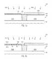
- FIG. 1 aschematically illustrates a cross-sectional view of a semiconductor device 100 at an early manufacturing stage.
- the device 100may comprise a substrate 101 , which may represent any appropriate carrier material for forming thereabove a silicon-containing semiconductor layer 102 .
- the substrate 101 in combination with the semiconductor layer 102may represent a silicon-on-insulator (SOI) configuration, when a buried insulating layer (not shown) may be provided between the semiconductor layer 102 and the substrate 101 .
- SOIsilicon-on-insulator
- the device 100may represent a “bulk” configuration in which the semiconductor layer 102 may represent an upper portion of a crystalline semiconductor material of the substrate 101 .
- an SOI configuration and a bulk configurationmay both be provided in the device 100 at different device areas, if considered appropriate for the overall performance and behavior of the semiconductor device 100 .
- an appropriate isolation structure 103for instance in the form of a shallow trench isolation, may be provided in the semiconductor layer 102 , thereby defining active regions 102 A, 102 B, which may be understood as silicon-containing semiconductor regions in and above which at least one transistor element is to be formed.
- the active region 102 Amay represent an appropriately doped silicon-based semiconductor material for forming therein and thereabove a P-channel transistor, while the active region 102 B may represent the active region of an N-channel transistor.
- a mask layer 104is formed above the active region 102 B and may be comprised of any appropriate material, such as silicon nitride, silicon dioxide and the like, which may substantially suppress oxidation of the semiconductor region 102 B or which may at least significantly reduce a corresponding oxidation rate during an oxidation process to be performed in a later manufacturing stage.
- the mask layer 104may comprise a silicon nitride material which may be considered as a non-oxidizable material for a plurality of oxidation atmospheres.
- the mask layer 104may comprise one or more additional layers, such as a layer 104 A, which may act as an efficient etch stop layer upon removing the mask layer 104 .
- the etch stop layer 104 Amay be comprised of a silicon dioxide material when the layer 104 may be provided in the form of a silicon nitride material.
- a layer of a semiconductor alloy 105such as a silicon/germanium alloy, may be formed on the active region 102 A and may thus represent a portion of the active region 102 A upon forming a transistor element therein in a later manufacturing stage.
- the semiconductor alloymay be provided with a specific thickness and with a germanium concentration that may comply with the available parameter setting of a corresponding deposition technique.
- the semiconductor alloy 105may be formed with a reduced degree of lattice defects, while a corresponding adaptation of the concentration of the non-silicon species contained therein, such as the germanium species, may be accomplished by subsequent well-controllable manufacturing processes in order to enhance overall uniformity of the finally obtained threshold adjusting semiconductor alloy.
- the semiconductor alloy 105may have a thickness of approximately 5-20 ⁇ and may have a germanium concentration of approximately 15-25 atomic percent germanium if a silicon/germanium alloy is considered.
- the germanium concentrationmay be approximately 23 atomic percent and less.
- the semiconductor device 100 as illustrated in FIG. 1 amay be formed on the basis of the following processes.
- the basic doping in the active regions 102 A, 102 Bmay be established by, for instance, ion implantation using appropriate masking regimes on the basis of well-established strategies. If required, an anneal process may be performed to activate the dopants and re-crystallize implantation-induced damage.
- the mask layer 104possibly in combination with the layer 104 A, may be formed, for instance, by oxidation and/or deposition for the layer 104 A and by deposition of the layer 104 .
- the layer 104 Afor instance in the form of a silicon dioxide material
- an appropriate silicon nitride materialmay be deposited and may subsequently be patterned on the basis of well-established lithography techniques, wherein the layer 104 A may be used as an etch stop material, for instance for maintaining integrity of the active region 102 B.
- the exposed portion of the layer 104 Amay be removed on the basis of highly controllable etch recipes, such as hydrofluoric acid and the like, if a silicon dioxide material is considered.
- the surface of the active region 102 Amay be prepared for the deposition of the layer 105 , which may be accomplished by performing one or more cleaning processes in order to remove silicon oxide residues together with other contaminants and the like that may have deposited on the exposed surface portion during the preceding manufacturing processes.
- the semiconductor device 100may be exposed to the ambient of a selective epitaxial growth process 106 in order to provide the material 105 with a high degree of uniformity on the basis of well-established parameter settings. For instance, by selecting an appropriate substrate temperature in the range of approximately 500-800° C.
- the layer 105may deposit with a specific concentration of the non-silicon species, such as germanium, while a significant deposition of material on the mask layer 104 may be suppressed.
- a specific concentration of the non-silicon speciessuch as germanium
- enhanced process uniformitymay be achieved by maintaining the concentration of the non-silicon species by approximately 25 percent and less, if a silicon/germanium alloy is considered.
- silicon-containing semiconductor alloyssuch as silicon/tin, silicon/germanium/tin, silicon/carbon, other appropriate and well-approved parameter settings may be selected so as to obtain a highly uniform process result.
- FIG. 1 bschematically illustrates the semiconductor device 100 in a further advanced manufacturing stage when exposed to an oxidizing ambient 107 .
- the oxidizing ambient 107may be established in any appropriate process tool, such as a furnace, at temperatures of approximately 900° C. and higher, so as to perform a dry oxidation process during which oxygen may diffuse into the layer 105 and may preferably react with the silicon species, thereby increasingly consuming the silicon species and forming an oxidized portion 105 A, while the non-silicon species such as the germanium species may be driven out from the oxidized portion 105 A and may thus diffuse into a remaining layer 105 B, thereby increasing the concentration of the non-silicon species therein.
- the oxidation rate during the process 107may be well controllable and may also exhibit a high degree of uniformity across the entire substrate 101 , which may typically be better than the uniformity obtained by the epitaxial growth process 106 of FIG. 1 a . Consequently, the oxidation process 107 may not contribute to a pronounced further process non-uniformity during the formation of an appropriate semiconductor alloy.
- the oxidized portion 105 A and thus the remaining semiconductor alloy 105 Bmay be provided with well-controllable thickness values, while the enrichment with the non-silicon species may also be achieved in a well-controllable manner. Due to the presence of the mask 104 , a significant oxidation of the active region 102 B may be reliably avoided.
- FIG. 1 cschematically illustrates the semiconductor device 100 when exposed to an etch ambient 108 , which may established on the basis of well-established selective etch recipes, such as hydrofluoric acid, in order to remove the portion 105 A with a high degree of selectivity with respect to the remaining layer of the semiconductor alloy 105 B having the increased concentration of the non-silicon species. Consequently, after removing the oxidized portion 105 A, the layer 105 B may have an increased germanium concentration which may be required for adjusting the threshold voltage of a transistor still to be formed in and above the active region 102 A.
- an etch ambient 108which may established on the basis of well-established selective etch recipes, such as hydrofluoric acid
- the thickness of the layer 105 B and/or the concentration of the germanium speciesmay require a further adaptation with respect to the desired transistor characteristics, further oxidation and removal processes, possibly in combination with a preceding additional epitaxial growth process, may be performed, as will be described later on in more detail.
- the further processingmay be continued by forming a gate electrode structure including high-k dielectric materials and metal-containing electrode materials, as will be explained later on in more detail.
- the etch sequence 108may also comprise any cleaning processes for preparing the surface of the layer 105 B for a further epitaxial growth process.
- material of the isolation structure 103may also be removed, i.e., of an exposed portion thereof, as indicated by the dashed line 103 A. A corresponding material removal may, however, not substantially affect the further processing of the device 100 .
- FIG. 1 dschematically illustrates the semiconductor device 100 when exposed to a further selective epitaxial growth process 109 , which may be performed on the basis of the same parameter setting as the process 106 of FIG. 1 a .
- a different parameter settingmay be used when a desired degree of uniformity of the deposition process 109 may be achieved. Consequently, a further silicon-containing semiconductor alloy 110 may be formed on the previous layer 105 B, wherein the characteristics of the layer 110 may also be adjusted by an oxidation and etch sequence, if required.
- the further processingmay be performed on the basis of the layers 105 B, 110 by forming an appropriate gate electrode structure.
- FIG. 1 eschematically illustrates the semiconductor device 100 when exposed to a further oxidizing ambient 111 , which may be established on the basis of similar parameter settings as described above with reference to FIG. 1 b , while, in other cases, any other appropriate parameters may be selected, depending on the characteristics of the layer 110 . Consequently, during the process 111 , an oxidized portion 110 A may be formed, thereby also modifying the material composition of a remaining portion 110 B, similarly as previously explained.
- one or both oxidation processes 107 ( FIG. 1 b ) and 111may be performed as “locally selective” anneal processes so as to enable an individual adaptation of the characteristics of the layers 105 A and/or 110 B.
- laser-based or flashlight-based anneal techniquesmay be applied in which appropriate scan patterns or masking regimes may be used so as to locally form the oxidized portion 110 A or by locally adapting the oxidation rate so as to obtain different types of layers 105 B and/or 110 B.
- FIG. 1 fschematically illustrates the semiconductor device 100 during a further etch process 112 in order to remove the oxidized portion 110 A ( FIG. 1 e ).
- similar etch recipesmay be used as previously described. Consequently, the remaining semiconductor layers 110 B, 105 B may form a layer of a semiconductor material 113 having a specific thickness 113 T and a specific material composition as adjusted during the previous deposition, oxidation and etch sequences.
- the layer 113 in the form of a silicon/germanium layermay have a thickness of approximately 5-15 ⁇ with a germanium concentration of more than 25 atomic percent, while, in other cases, any other appropriate values for the thickness 113 T and the germanium concentration may be adjusted.
- a further recessing of the isolation structure 103indicated by 103 B, may be created.
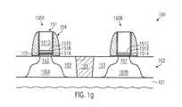
- FIG. 1 gschematically illustrates the semiconductor device 100 in an advanced manufacturing stage.
- a first transistor 150 Asuch as a P-channel transistor
- a second transistor 150 Bsuch as an N-channel transistor
- the transistors 150 A, 150 Bmay comprise a gate electrode structure 151 comprising a sophisticated stack of layers, such as layers 151 A, 151 B and 151 C, which may represent a high-k gate insulation layer, for instance in the form of the layers 151 A and 151 B, wherein at least one of these layers may be comprised of the material having a dielectric constant of 10.0 and higher.
- the layer 151 Amay be provided in the form of a “conventional” dielectric material, such as a silicon-containing oxide material and the like, and may provide superior interface characteristics, as previously described. For example, a thickness of 5-10 ⁇ may be used for the layer 151 A.
- the layer 151 Bmay represent any appropriate high-k material, such as hafnium oxide and the like, with an appropriate thickness, for instance of approximately 10-30 ⁇ , followed by the layer 151 C, which may represent a metal-containing electrode material, such as titanium nitride, aluminum oxide and the like.
- a further electrode material 151 Dfor instance in the form of polysilicon, germanium, a silicon/germanium mixture and the like, may be formed on the metal-containing electrode material 151 C.
- a similar configurationmay be provided in the gate electrode structure of the transistor 150 B.
- the transistors 150 A, 150 Bmay comprise a channel region 152 , which may be laterally enclosed by corresponding drain and source regions 153 .
- the channel region 152 in the action region 102 Amay comprise the silicon-containing semiconductor alloy 113 having characteristics as adjusted during the previous process sequence.
- a spacer structure 154may be formed on sidewalls of the gate electrode structure 151 .
- the transistors 150 A, 150 Bmay be formed on the basis of the following process techniques. After providing the layer 113 in the active region 102 A and after removal of the mask layer 104 ( FIG. 1 f ), the material layers 151 A, 151 B, 151 C and 151 D may be formed in accordance with well-established process techniques followed, by the sophisticated patterning sequence in order to obtain the gate electrode structures 151 . Thereafter, appropriate implantation processes may be performed, possibly in combination with forming the spacer structure 154 , in order to establish a desired dopant profile for the drain and source regions 153 . Thereafter, any anneal cycles may be performed to activate the dopant species and also re-crystallize implantation-induced damage.
- the further processingmay be continued, for instance by forming metal silicide regions in the drain and source regions 153 and providing an appropriate interlayer dielectric material for forming contact elements therein, wherein, if desired, additional strain-inducing mechanisms, for instance in the form of a stressed dielectric material, may be provided.
- a strain-inducing semiconductor alloymay be formed adjacent to a gate electrode structure.
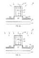
- FIG. 2 aschematically illustrates a semiconductor device 200 comprising a substrate 201 and a semiconductor layer 202 .
- a gate electrode structure 251may be formed on a portion of the semiconductor layer 202 and may be encapsulated by a mask material 204 , for instance in the form of silicon nitride, silicon dioxide and the like.
- the gate electrode structure 251may have any appropriate configuration, such as a gate insulation layer 251 A in combination with an electrode material 251 D.
- the gate insulation layer 251 A in combination with the electrode material 251 Dmay represent a “conventional” gate electrode structure, that is, dielectric materials such as silicon dioxide, silicon nitride, silicon oxynitride and the like may be used for the layer 251 A in combination with silicon, silicon/germanium, germanium and the like for the electrode material 251 D.
- the gate electrode structure 251may represent a sophisticated gate electrode structure in which the gate insulation layer 251 A may comprise a high-k dielectric material, as previously explained.
- the electrode material 251 Dmay comprise a metal-containing material that may be formed on the gate insulation layer 251 A, as previously discussed.
- a channel region 252may represent a silicon material, while, in other cases, additionally, a threshold adjusting semiconductor alloy 213 may be provided and may have appropriately adjusted characteristics in view of obtaining a desired band gap offset, as previously explained.
- cavities 202 Care formed in the semiconductor layer 202 laterally offset from the gate electrode structure 251 .
- a first layer of strain-inducing semiconductor alloy 220such as a silicon/germanium alloy, may be formed in the cavities 202 C.
- the semiconductor alloy 220may have a concentration of a non-silicon species, which may be adapted on the basis of subsequent process steps, while not unduly contributing to increased crystal defects and the like.
- the semiconductor device 200 as shown in FIG. 2 amay be formed on the basis of the following processes. After defining corresponding active regions on the basis of an isolation structure, as previously discussed with reference to the device 100 , if required, the threshold adjusting semiconductor alloy 213 may be formed, wherein, in some illustrative embodiments, at least one deposition, oxidation and etch cycle may be used so as to adjust the overall characteristics of the material 213 , as previously described with reference to the semiconductor device 100 . In other cases, the material 213 may not be provided and the further processing may be continued by forming the gate electrode structure 251 , which may be appropriately encapsulated by providing a cap layer 251 E in combination with the spacers 204 .
- an etch processmay be performed in order to obtain the cavities 202 C and, after preparing the exposed surface portion, a selective epitaxial growth process 206 may be performed in order to provide the layer 220 having specific characteristics with respect to thickness, material composition and the like, as previously explained.
- an appropriate parameter setting for the process 206may be selected so as to obtain the layer 220 with a high degree of uniformity and a reduced defect rate, while other parameters such as the overall germanium concentration, if a silicon/germanium alloy is considered, may be adjusted in a later manufacturing stage.
- FIG. 2 bschematically illustrates the semiconductor device when exposed to an oxidizing ambient 207 in which a portion 220 A of the layer 220 may be oxidized, while preserving a portion 220 B, which may thus have modified characteristics, for instance with respect to the concentration of a non-silicon species.
- FIG. 2 cschematically illustrates the semiconductor device 200 during an etch process 208 for selectively removing the portion 220 A while substantially maintaining the semiconductor alloy 220 B.
- similar etch recipesmay be used, as previously explained with reference to the device 100 .
- FIG. 2 dschematically illustrates the semiconductor device 200 in a further advanced manufacturing stage.
- one or more additional layers of the strain-inducing semiconductor alloyindicated as 221 B, 222 B, 223 B, may be formed in the cavities 202 C ( FIG. 2 c ).
- the layers 221 B, 222 B, 223 Bmay have similar characteristics in view of material composition as the layer 220 B, while, in other cases, different characteristics may be adjusted, for instance by applying a process sequence described above for only some of the layers 221 B, 222 B, 223 B, or by selecting different process parameters, for instance during the oxidation process and the like.
- each of the individual semiconductor layersmay be deposited on the basis of a desired parameter setting of the selective epitaxial growth process and, if required, the material composition of one or more of these layers may be appropriately adjusted by applying an oxidation and etch cycle, as described above.
- an increased degree of germanium concentrationmay be accomplished, at least in some areas, within cavities 202 C without introducing significant lattice defects or differing from superior process non-uniformities, as may typically be the case in conventional process strategies in which the germanium concentration may be increased in a selective epitaxial growth process.
- the processing of the device 200may be continued by removing the spacer 204 and the cap layer 251 E and forming drain and source regions, as is previously described with reference to the semiconductor device 100 .
- the present disclosureprovides techniques for varying the characteristics of a silicon-containing semiconductor alloy in a highly controllable manner by using a stable and uniform deposition recipe for a selective epitaxial growth process and performing at least one oxidation and etch cycle for modifying the characteristics, for instance increasing the germanium concentration in a silicon/germanium alloy.
- enhanced flexibilitymay be accomplished, for instance, for providing a threshold adjusting silicon/germanium alloy and/or providing a strain-inducing semiconductor alloy in drain and source areas of sophisticated transistors.
Landscapes
- Insulated Gate Type Field-Effect Transistor (AREA)
- Metal-Oxide And Bipolar Metal-Oxide Semiconductor Integrated Circuits (AREA)
Abstract
Description
- 1. Field of the Invention
- Generally, the present disclosure relates to sophisticated integrated circuits including advanced transistor elements that comprise highly capacitive gate structures including a metal-containing electrode and a high-k gate dielectric of increased permittivity compared to conventional gate dielectrics, such as silicon dioxide and silicon nitride.
- 2. Description of the Related Art
- The fabrication of advanced integrated circuits, such as CPUs, storage devices, ASICs (application specific integrated circuits) and the like, requires a large number of circuit elements to be formed on a given chip area according to a specified circuit layout, wherein field effect transistors represent one important type of circuit element that substantially determines performance of the integrated circuits. Generally, a plurality of process technologies are currently practiced, wherein, for many types of complex circuitry including field effect transistors, MOS technology is currently one of the most promising approaches due to the superior characteristics in view of operating speed and/or power consumption and/or cost efficiency. During the fabrication of complex integrated circuits using, for instance, MOS technology, millions of transistors, e.g., N-channel transistors and/or P-channel transistors, are formed on a substrate including a crystalline semiconductor layer. A field effect transistor, irrespective of whether an N-channel transistor or a P-channel transistor is considered, typically comprises so-called PN junctions that are formed by an interface of highly doped regions, referred to as drain and source regions, with a slightly doped or non-doped region, such as a channel region, disposed adjacent to the highly doped regions. In a field effect transistor, the conductivity of the channel region, i.e., the drive current capability of the conductive channel, is controlled by a gate electrode formed adjacent to the channel region and separated therefrom by a thin insulating layer. The conductivity of the channel region, upon formation of a conductive channel due to the application of an appropriate control voltage to the gate electrode, depends on the dopant concentration, the mobility of the charge carriers and, for a given extension of the channel region in the transistor width direction, on the distance between the source and drain regions, which is also referred to as channel length. Hence, in combination with the capability of rapidly creating a conductive channel below the insulating layer upon application of the control voltage to the gate electrode, the conductivity of the channel region substantially affects the performance of MOS transistors. Thus, as the speed of creating the channel, which depends on the conductivity of the gate electrode, and the channel resistivity substantially determine the transistor characteristics, the scaling of the channel length, and associated therewith the reduction of channel resistivity and reduction of gate resistivity, is a dominant design criterion for accomplishing an increase in the operating speed of the integrated circuits.
- Presently, the vast majority of integrated circuits are fabricated on the basis of silicon due to the substantially unlimited availability thereof, the well-understood characteristics of silicon and related materials and processes and the experience gathered over the last 50 years.
- Therefore, silicon will likely remain the material of choice in the foreseeable future for circuit generations designed for mass products. One reason for the importance of silicon in fabricating semiconductor devices has been the superior characteristics of a silicon/silicon dioxide interface that allows reliable electrical insulation of different regions from each other. The silicon/silicon dioxide interface is stable at high temperatures and, thus, allows the performance of subsequent high temperature processes, as are required, for example, for anneal cycles to activate dopants and to cure crystal damage without sacrificing the electrical characteristics of the interface.
- For the reasons pointed out above, in field effect transistors, silicon dioxide has been preferably used as a gate insulation layer that separates the gate electrode, frequently comprised of polysilicon or other materials, from the silicon channel region. In steadily improving device performance of field effect transistors, the length of the channel region has continuously been decreased to improve switching speed and drive current capability. Since the transistor performance is controlled by the voltage supplied to the gate electrode, to invert the surface of the channel region to a sufficiently high charge density for providing the desired drive current for a given supply voltage, a certain degree of capacitive coupling, provided by the capacitor formed by the gate electrode, the channel region and the silicon dioxide disposed therebetween, has to be maintained. It turns out that decreasing the channel length requires an increased capacitive coupling to avoid the so-called short channel behavior during transistor operation. The short channel behavior may lead to an increased leakage current and to a pronounced dependence of the threshold voltage on the channel length. Aggressively scaled transistor devices with a relatively low supply voltage and thus reduced threshold voltage may suffer from an exponential increase of the leakage current for the required increased capacitive coupling of the gate electrode to the channel region, since the thickness of the silicon dioxide layer has to be correspondingly decreased to provide the required capacitance between the gate and the channel region. For example, a channel length of approximately 0.08 μm may require a gate dielectric made of silicon dioxide as thin as approximately 1.2 nm. Although, generally, usage of high speed transistor elements having an extremely short channel may be restricted to high speed applications, whereas transistor elements with a longer channel may be used for less critical applications, such as storage transistor elements, the relatively high leakage current caused by direct tunneling of charge carriers through an ultra-thin silicon dioxide gate insulation layer may reach values for an oxide thickness in the range or 1-2 nm that may no longer be compatible with requirements for performance driven circuits.
- Therefore, replacing silicon dioxide as the material for gate insulation layers has been considered, particularly for transistors requiring extremely thin silicon dioxide gate layers. Possible alternative dielectrics include materials that exhibit a significantly higher permittivity so that a physically greater thickness of a correspondingly formed gate insulation layer nevertheless provides a capacitive coupling that would be obtained by an extremely thin silicon dioxide layer.
- It has thus been suggested to replace silicon dioxide with high permittivity materials such as tantalum oxide (Ta2O5) with a k of approximately 25, strontium titanium oxide (SrTiO3) having a k of approximately 150, hafnium oxide (HfO2), HfSiO, zirconium oxide (ZrO2) and the like.
- When advancing to sophisticated gate architectures based on high-k dielectrics, transistor performance may also be increased by providing an appropriate conductive material for the gate electrode to replace the usually used polysilicon material, since polysilicon may suffer from charge carrier depletion at the vicinity of the interface to the gate dielectric, thereby reducing the effective capacitance between the channel region and the gate electrode. Thus, a gate stack has been suggested in which a high-k dielectric material provides enhanced capacitance even at a less critical thickness compared to a silicon dioxide layer, while maintaining leakage currents at an acceptable level. On the other hand, metal-containing non-polysilicon materials, such as titanium nitride and the like, may be formed so as to directly connect to the high-k dielectric material, thereby substantially avoiding the presence of a depletion zone. Since, typically, a low threshold voltage of the transistor, which represents the voltage at which a conductive channel forms in the channel region, is desired to obtain the high drive currents, commonly, the controllability of the respective channel requires pronounced lateral dopant profiles and dopant gradients, at least in the vicinity of the PN junctions. Therefore, so-called halo regions are usually formed by ion implantation in order to introduce a dopant species whose conductivity type corresponds to the conductivity type of the remaining channel and semiconductor region so as to “reinforce” the resulting PN junction dopant gradient after the formation of respective extension and deep drain and source regions. In this way, the threshold voltage of the transistor significantly determines the controllability of the channel, wherein a significant variance of the threshold voltage may be observed for reduced gate lengths. Hence, by providing an appropriate halo implantation region, the controllability of the channel may be enhanced, thereby also reducing the variance of the threshold voltage, which is also referred to as threshold roll off, and also reducing significant variations of transistor performance with a variation in gate length. Since the threshold voltage of the transistors is significantly determined by the work function of the gate material that is in contact with the gate dielectric material, an appropriate adjustment of the effective work function with respect to the conductivity type of the transistor under consideration has to be guaranteed.
- For example, appropriate metal-containing gate electrode materials, such as titanium nitride, aluminum oxide and the like, may frequently be used, wherein the corresponding work function may be adjusted so as to be appropriate for one type of transistor, such as N-channel transistors, while P-channel transistors may require a different work function and thus a differently treated titanium nitride material or any other appropriate metal-containing material in order to obtain the desired threshold voltage. In this case, complex and sophisticated manufacturing regimes may be required to provide different gate electrode materials in order to comply with the requirements of different transistor types. For this reason, it has also been proposed to appropriately adjust the threshold voltage of transistor devices by providing a specifically designed semiconductor material at the interface between the high-k dielectric material and the channel region of the transistor device, in order to appropriately “adapt” the band gap of the specifically designed semiconductor material to the work function of the metal-containing gate electrode material, thereby obtaining the desired low threshold voltage of the transistor under consideration.
- The adjustment of the band gap and thus of the threshold of sophisticated transistor elements on the basis of silicon/germanium is a promising approach for sophisticated transistor elements comprising a metal gate. Typically, the silicon/germanium material may be formed on the basis of selective epitaxial growth techniques in which process parameters may be controlled such that a significant material deposition may be restricted to crystalline silicon areas only, while a significant deposition on dielectric surface areas may be efficiently suppressed. During this epitaxial growth process, parameter values, such as flow rates of precursor gases, deposition pressure, temperature and the like, may have to be precisely controlled in order to accomplish a high degree of uniformity of the material characteristics of the silicon/germanium alloy across the entire substrate surface. For example, a delicate balance between layer thickness, lattice mismatch between the silicon/germanium alloy and the silicon material, temperature during the process and density of the deposited material may have to be maintained in order to obtain a substantially defect-free silicon/germanium alloy. Moreover, in view of appropriately adjusting the band gap of the silicon/germanium alloy in view of the desired threshold voltage, the germanium concentration and the resulting layer thickness may represent very critical parameters, which may not be adjusted independently with respect to other process parameters, while, at the same time, even minute variations in concentration and layer thickness may result in a significant threshold variability across individual die regions and also across the entire semiconductor substrate. Consequently, in sophisticated semiconductor production facilities, only a restricted number of different parameter settings may typically be applied for various semiconductor products when a silicon/germanium alloy may be required, for instance for adjusting the threshold of sophisticated transistor elements. For example, a less than desired germanium concentration may be achieved on the basis of a well-controllable and reliable manufacturing process in a sophisticated semiconductor facility, thereby significantly restricting the flexibility in adjusting the overall transistor characteristics.
- It is also well known that the switching speed and the drive current capability of silicon-based field effect transistors may be increased by modifying the lattice structure in the channel region of the transistors. That is, by creating compressive or tensile strain in the channel region of the transistor, the charge carrier mobility may be increased, thereby achieving the desired increase of transistor performance. For example, a compressive strain component induced along the current flow direction of a P-channel transistor for a standard crystallographic configuration of the silicon in the channel region, i.e., a (100) surface orientation with the current flow direction being aligned along a <110> crystallographic axis, may provide a significant increase of the hole mobility. Thus, frequently, a silicon/germanium alloy may be incorporated into the drain and source areas of P-channel transistors which may thus be provided in a highly strained state due to the lattice mismatch between the silicon/germanium alloy and the surrounding silicon material, thereby also inducing corresponding compressive strain components in the adjacent channel region of the transistor. The silicon/germanium alloy may be formed in the drain and source areas by first providing appropriate cavities and re-filling the cavities on the basis of a selective epitaxial growth process, wherein the magnitude of the resulting strain component may be adjusted on the basis of a lateral offset of the cavities with respect to the channel region and the germanium concentration, which may determine the magnitude of the lattice mismatch. Also in this case, appropriate deposition recipes may typically be available in a sophisticated semiconductor facility to enable a substantially defect-free deposition of the silicon/germanium alloy with a maximum germanium concentration that may be compatible with the above-explained constraints in view of the parameter setting.
- Consequently, although well-established process recipes may be available for forming a silicon/germanium alloy in a controllable manner, the available parameter settings may not provide sufficient flexibility in adjusting the overall transistor characteristics, such as threshold voltage and the like.
- The present disclosure is directed to various methods that may avoid, or at least reduce, the effects of one or more of the problems identified above.
- The following presents a simplified summary of the invention in order to provide a basic understanding of some aspects of the invention. This summary is not an exhaustive overview of the invention. It is not intended to identify key or critical elements of the invention or to delineate the scope of the invention. Its sole purpose is to present some concepts in a simplified form as a prelude to the more detailed description that is discussed later.
- Generally, the present disclosure provides techniques for extending the capabilities of presently available well-established process recipes for forming a silicon-containing semiconductor alloy, such as a silicon/germanium alloy, for instance with respect to increasing the concentration of a non-silicon species, such as a germanium species, without contributing to increased processed non-uniformity and substantially without generating additional crystalline defects. To this end, the silicon-containing semiconductor alloy may be formed on the basis of a well-established process recipe and subsequently adjusting the concentration of the non-silicon species, for instance increasing the concentration thereof by an oxidation process in which preferably the silicon species may be consumed so as to form a corresponding oxide while the non-silicon species may be “driven” into the remaining non-oxidized portion of the previously formed semiconductor alloy. Thereafter, the oxidized portion may be selectively removed and thus a corresponding silicon-containing semiconductor alloy may be obtained with a modified concentration, substantially without contributing to additional crystal defects. Furthermore, the oxidation process as well as the selective removal may be performed with a high degree of process uniformity, thereby substantially not contributing to the overall process non-uniformity, which may substantially be determined by the initially performed epitaxial growth process. If required, a sequence of deposition of an alloy, oxidizing the same and removing the oxidized portion may be repeated one or several times to obtain a desired total thickness of the silicon-containing semiconductor alloy having the modified concentration of the non-silicon species. In other cases, at least the process of oxidizing a portion of a semiconductor alloy and selectively removing the oxidized portion may be repeated to further increase the concentration of the non-silicon species, wherein an initial layer thickness may be appropriately selectable so as to obtain a desired final thickness after removing two or more oxidized portions. In some illustrative embodiments, the adaptation of the concentration of a non-silicon species may be applied to the formation of a threshold adjusting material in order to obtain a desired band gap offset in forming sophisticated gate electrode structures on the basis of high-k dielectric materials and metal-containing electrode materials. In still other illustrative aspects disclosed herein, the increased concentration of a non-silicon species may be applied to providing a strain-inducing semiconductor alloy in the drain and source areas of transistor elements with an increased internal strain level, while not unduly contributing to an increased degree of lattice defects, such as dislocations, which may frequently be associated when increasing the contents of a non-silicon species. In still other illustrative embodiments disclosed herein, the concept of adjusting the material composition of a silicon-containing semiconductor alloy may be applied to both the threshold adjusting and the strain engineering of a transistor element, thereby providing enhanced flexibility in individually adjusting the characteristics of the various semiconductor alloys on the basis of a single well-established process recipe.
- One illustrative method disclosed herein comprises forming a first layer of a silicon-containing semiconductor alloy on a silicon-containing crystalline semiconductor region, wherein the silicon-containing semiconductor alloy comprises a non-silicon species with a first concentration. The method additionally comprises forming an oxide by consuming material of the first layer of a silicon-containing semiconductor alloy while preserving a second layer of a silicon-containing semiconductor alloy on the silicon-containing semiconductor region, wherein the second layer of a silicon-containing semiconductor alloy comprises the non-silicon species with a second concentration. Furthermore, the oxide is removed from the second layer of a silicon-containing semiconductor alloy. Finally, the method comprises forming a gate electrode structure of a transistor above the second layer of a silicon-containing semiconductor alloy, wherein the gate electrode structure comprises a high-k dielectric gate insulation layer and a metal-containing gate electrode material formed above the high-k dielectric gate insulation layer.
- A further illustrative method disclosed herein comprises forming a first layer of a silicon/germanium alloy on a silicon-containing semiconductor region, wherein the first layer comprises a germanium species with a first concentration. The method further comprises oxidizing a portion of the first layer of a silicon/germanium alloy so as to form a second layer of a silicon/germanium alloy, wherein the second layer comprises the germanium species with a second concentration that is higher than the first concentration. Furthermore, the portion is moved selectively to the second layer of a silicon/germanium alloy and a transistor element is formed in and on the silicon-containing semiconductor region on the basis of the second layer of a silicon/germanium alloy.
- A still further illustrative method disclosed herein comprises forming a cavity in a silicon-containing semiconductor region laterally adjacent to a gate electrode structure of a transistor. The method further comprises forming a first layer of a silicon-containing semiconductor alloy in the cavity, wherein the first layer comprises a non-silicon species with a first concentration. The method additionally comprises oxidizing a portion of the first layer of a silicon-containing semiconductor alloy so as to form a second layer of a silicon-containing semiconductor alloy, wherein the second layer comprises the non-silicon species with a second concentration that is higher than the first concentration. Moreover, the method comprises forming drain and source regions in the silicon-containing semiconductor region.
- The disclosure may be understood by reference to the following description taken in conjunction with the accompanying drawings, in which like reference numerals identify like elements, and in which:
FIGS. 1 a-1cschematically illustrate cross-sectional views of a semiconductor device during a process sequence for forming a silicon-containing semiconductor alloy and modifying the material composition thereof in a portion by performing an oxidation process and removing an oxidized portion, according to illustrative embodiments;FIGS. 1 d-1fschematically illustrate cross-sectional views of the semiconductor device according to further illustrative embodiments in which the sequence of depositing the semiconductor alloy, oxidizing a portion thereof and removing the oxidized portion may be repeated;FIG. 1 gschematically illustrates a cross-sectional view of the semiconductor device in a further advanced manufacturing stage in which the previously formed silicon-containing semiconductor alloy may be used as a threshold adjusting material for one type of transistor that may include a sophisticated gate electrode structure, according to still further illustrative embodiments; andFIGS. 2 a-2dschematically illustrate cross-sectional views of a semiconductor device during various manufacturing stages in which a strain-inducing semiconductor alloy may be formed on the basis of a process sequence for adjusting the concentration of a non-silicon species by oxidation and selective removal, according to illustrative embodiments, wherein a threshold adjustment may also be accomplished by the corresponding process sequence described above.- While the subject matter disclosed herein is susceptible to various modifications and alternative forms, specific embodiments thereof have been shown by way of example in the drawings and are herein described in detail. It should be understood, however, that the description herein of specific embodiments is not intended to limit the invention to the particular forms disclosed, but on the contrary, the intention is to cover all modifications, equivalents, and alternatives falling within the spirit and scope of the invention as defined by the appended claims.
- Various illustrative embodiments of the invention are described below. In the interest of clarity, not all features of an actual implementation are described in this specification. It will of course be appreciated that in the development of any such actual embodiment, numerous implementation-specific decisions must be made to achieve the developers' specific goals, such as compliance with system-related and business-related constraints, which will vary from one implementation to another. Moreover, it will be appreciated that such a development effort might be complex and time-consuming, but would nevertheless be a routine undertaking for those of ordinary skill in the art having the benefit of this disclosure.
- The present subject matter will now be described with reference to the attached figures. Various structures, systems and devices are schematically depicted in the drawings for purposes of explanation only and so as to not obscure the present disclosure with details that are well known to those skilled in the art. Nevertheless, the attached drawings are included to describe and explain illustrative examples of the present disclosure. The words and phrases used herein should be understood and interpreted to have a meaning consistent with the understanding of those words and phrases by those skilled in the relevant art. No special definition of a term or phrase, i.e., a definition that is different from the ordinary and customary meaning as understood by those skilled in the art, is intended to be implied by consistent usage of the term or phrase herein. To the extent that a term or phrase is intended to have a special meaning, i.e., a meaning other than that understood by skilled artisans, such a special definition will be expressly set forth in the specification in a definitional manner that directly and unequivocally provides the special definition for the term or phrase.
- Generally, the present disclosure provides techniques for forming a silicon-containing semiconductor alloy on the basis of enhanced flexibility by extending the capabilities of existing well-established recipes in that the concentration of a non-silicon species may be adjusted by performing a well-controllable oxidation process and selectively removing the oxidized portion, thereby efficiently modifying the material composition in the remaining part of the previously deposited semiconductor alloy. In some illustrative embodiments, silicon/germanium alloy may be adapted in view of the germanium concentration without unduly contributing to the overall defect rate by oxidizing a portion of the silicon/germanium alloy, for instance upon establishing an appropriate oxidation ambient, such as a dry oxidation at elevated temperatures of approximately 900° C. and above, during which the silicon species may preferably react with the oxygen, while the germanium species may be driven out of the oxidized portion thereby increasing the germanium concentration in the remaining semiconductor alloy. Since the oxidation process may be performed on the basis of well-controllable process conditions, that is, corresponding oxidation processes may be performed by using well-established parameter settings in which the resulting oxidation rate may be predicted with a high degree of reliability, the oxidation of the portion of the silicon/germanium alloy may be accomplished with a high degree of controllability and also the selective removal thereof may be performed on the basis of well-established etch techniques, for instance using diluted hydrofluoric acid (HF) and the like. Consequently, in total, based on an initial selective epitaxial growth recipe with a desired degree of process uniformity, any additional process variations may be kept at a very low level compared to epitaxial growth techniques in which the germanium concentration is to be increased, for instance, in adjusting a required band gap offset, providing a desired high strain component and the like. Consequently, a very efficient process sequence may be provided for implementing silicon/germanium alloys with a high degree of flexibility with respect to germanium concentration, layer thickness and the like on the basis of only one or a few well-established parameter settings for the complex selective epitaxial growth process, thereby reducing overall yield losses in semiconductor facilities when sophisticated semiconductor devices are to be formed. It should be appreciated that the principles disclosed herein may be efficiently applied to silicon/germanium alloys since this material mixture may frequently be used in sophisticated transistor elements. In other cases, the principles may be applied to other silicon-containing semiconductor materials in which the oxidation rate may differ for the various non-silicon species, thereby resulting in a corresponding reduction or increase of the concentration of the non-silicon species in the remaining portion of the previously formed semiconductor alloy.
FIG. 1 aschematically illustrates a cross-sectional view of asemiconductor device 100 at an early manufacturing stage. As illustrated, thedevice 100 may comprise asubstrate 101, which may represent any appropriate carrier material for forming thereabove a silicon-containingsemiconductor layer 102. Furthermore, in some illustrative embodiments, thesubstrate 101 in combination with thesemiconductor layer 102 may represent a silicon-on-insulator (SOI) configuration, when a buried insulating layer (not shown) may be provided between thesemiconductor layer 102 and thesubstrate 101. In other cases, as illustrated, thedevice 100 may represent a “bulk” configuration in which thesemiconductor layer 102 may represent an upper portion of a crystalline semiconductor material of thesubstrate 101. It should be appreciated that an SOI configuration and a bulk configuration may both be provided in thedevice 100 at different device areas, if considered appropriate for the overall performance and behavior of thesemiconductor device 100. In the manufacturing stage shown, anappropriate isolation structure 103, for instance in the form of a shallow trench isolation, may be provided in thesemiconductor layer 102, thereby definingactive regions active region 102A may represent an appropriately doped silicon-based semiconductor material for forming therein and thereabove a P-channel transistor, while theactive region 102B may represent the active region of an N-channel transistor. Moreover, as illustrated, amask layer 104 is formed above theactive region 102B and may be comprised of any appropriate material, such as silicon nitride, silicon dioxide and the like, which may substantially suppress oxidation of thesemiconductor region 102B or which may at least significantly reduce a corresponding oxidation rate during an oxidation process to be performed in a later manufacturing stage. For example, themask layer 104 may comprise a silicon nitride material which may be considered as a non-oxidizable material for a plurality of oxidation atmospheres. Furthermore, if desired, themask layer 104 may comprise one or more additional layers, such as alayer 104A, which may act as an efficient etch stop layer upon removing themask layer 104. For example, theetch stop layer 104A may be comprised of a silicon dioxide material when thelayer 104 may be provided in the form of a silicon nitride material. Moreover, a layer of asemiconductor alloy 105, such as a silicon/germanium alloy, may be formed on theactive region 102A and may thus represent a portion of theactive region 102A upon forming a transistor element therein in a later manufacturing stage. As previously discussed, in sophisticated process techniques for forming advanced gate electrode structures including a high-k dielectric material in combination with a metal-containing electrode material, it may be necessary to appropriately adjust the band gap offset of a channel material of the transistor, which may be accomplished on the basis of a silicon-containing semiconductor alloy, wherein a uniform thickness and a desired concentration of a non-silicon species, such as a germanium species, may be required. Since the corresponding parameters may not be compatible with the deposition capabilities of available and well-controllable selective epitaxial growth techniques, the semiconductor alloy may be provided with a specific thickness and with a germanium concentration that may comply with the available parameter setting of a corresponding deposition technique. Consequently, thesemiconductor alloy 105 may be formed with a reduced degree of lattice defects, while a corresponding adaptation of the concentration of the non-silicon species contained therein, such as the germanium species, may be accomplished by subsequent well-controllable manufacturing processes in order to enhance overall uniformity of the finally obtained threshold adjusting semiconductor alloy. For example, thesemiconductor alloy 105 may have a thickness of approximately 5-20 Å and may have a germanium concentration of approximately 15-25 atomic percent germanium if a silicon/germanium alloy is considered. For example, the germanium concentration may be approximately 23 atomic percent and less.- The
semiconductor device 100 as illustrated inFIG. 1 amay be formed on the basis of the following processes. After forming theisolation structure 103, which may be accomplished by sophisticated lithography, etch, deposition, oxidation and planarization processes, the basic doping in theactive regions mask layer 104, possibly in combination with thelayer 104A, may be formed, for instance, by oxidation and/or deposition for thelayer 104A and by deposition of thelayer 104. For example, after forming thelayer 104A, for instance in the form of a silicon dioxide material, an appropriate silicon nitride material may be deposited and may subsequently be patterned on the basis of well-established lithography techniques, wherein thelayer 104A may be used as an etch stop material, for instance for maintaining integrity of theactive region 102B. Thereafter, the exposed portion of thelayer 104A may be removed on the basis of highly controllable etch recipes, such as hydrofluoric acid and the like, if a silicon dioxide material is considered. Next, the surface of theactive region 102A may be prepared for the deposition of thelayer 105, which may be accomplished by performing one or more cleaning processes in order to remove silicon oxide residues together with other contaminants and the like that may have deposited on the exposed surface portion during the preceding manufacturing processes. Next, thesemiconductor device 100 may be exposed to the ambient of a selectiveepitaxial growth process 106 in order to provide the material105 with a high degree of uniformity on the basis of well-established parameter settings. For instance, by selecting an appropriate substrate temperature in the range of approximately 500-800° C. and supplying appropriate precursor materials, which are well known from chemical vapor deposition (CVD) based deposition techniques, thelayer 105 may deposit with a specific concentration of the non-silicon species, such as germanium, while a significant deposition of material on themask layer 104 may be suppressed. As previously explained, typically, enhanced process uniformity may be achieved by maintaining the concentration of the non-silicon species by approximately 25 percent and less, if a silicon/germanium alloy is considered. For other silicon-containing semiconductor alloys, such as silicon/tin, silicon/germanium/tin, silicon/carbon, other appropriate and well-approved parameter settings may be selected so as to obtain a highly uniform process result. FIG. 1 bschematically illustrates thesemiconductor device 100 in a further advanced manufacturing stage when exposed to an oxidizing ambient107. In some illustrative embodiments, the oxidizing ambient107 may be established in any appropriate process tool, such as a furnace, at temperatures of approximately 900° C. and higher, so as to perform a dry oxidation process during which oxygen may diffuse into thelayer 105 and may preferably react with the silicon species, thereby increasingly consuming the silicon species and forming anoxidized portion 105A, while the non-silicon species such as the germanium species may be driven out from the oxidizedportion 105A and may thus diffuse into a remaininglayer 105B, thereby increasing the concentration of the non-silicon species therein. It should be appreciated that the oxidation rate during theprocess 107 may be well controllable and may also exhibit a high degree of uniformity across theentire substrate 101, which may typically be better than the uniformity obtained by theepitaxial growth process 106 ofFIG. 1 a. Consequently, theoxidation process 107 may not contribute to a pronounced further process non-uniformity during the formation of an appropriate semiconductor alloy. Thus, based on the initial thickness and the parameters of theoxidation process 107, the oxidizedportion 105A and thus the remainingsemiconductor alloy 105B may be provided with well-controllable thickness values, while the enrichment with the non-silicon species may also be achieved in a well-controllable manner. Due to the presence of themask 104, a significant oxidation of theactive region 102B may be reliably avoided.FIG. 1 cschematically illustrates thesemiconductor device 100 when exposed to an etch ambient108, which may established on the basis of well-established selective etch recipes, such as hydrofluoric acid, in order to remove theportion 105A with a high degree of selectivity with respect to the remaining layer of thesemiconductor alloy 105B having the increased concentration of the non-silicon species. Consequently, after removing the oxidizedportion 105A, thelayer 105B may have an increased germanium concentration which may be required for adjusting the threshold voltage of a transistor still to be formed in and above theactive region 102A. If the thickness of thelayer 105B and/or the concentration of the germanium species may require a further adaptation with respect to the desired transistor characteristics, further oxidation and removal processes, possibly in combination with a preceding additional epitaxial growth process, may be performed, as will be described later on in more detail. In other cases, when the characteristics of thelayer 105B are appropriate for the threshold adjusting effect, the further processing may be continued by forming a gate electrode structure including high-k dielectric materials and metal-containing electrode materials, as will be explained later on in more detail.- In other cases, when additional process steps may be required, such as a further epitaxial growth process, the
etch sequence 108 may also comprise any cleaning processes for preparing the surface of thelayer 105B for a further epitaxial growth process. Furthermore, it should be appreciated that, during theetch process 108, material of theisolation structure 103 may also be removed, i.e., of an exposed portion thereof, as indicated by the dashedline 103A. A corresponding material removal may, however, not substantially affect the further processing of thedevice 100. FIG. 1 dschematically illustrates thesemiconductor device 100 when exposed to a further selectiveepitaxial growth process 109, which may be performed on the basis of the same parameter setting as theprocess 106 ofFIG. 1 a. In other cases, a different parameter setting may be used when a desired degree of uniformity of thedeposition process 109 may be achieved. Consequently, a further silicon-containingsemiconductor alloy 110 may be formed on theprevious layer 105B, wherein the characteristics of thelayer 110 may also be adjusted by an oxidation and etch sequence, if required. In other cases, if a graded concentration may be required, the further processing may be performed on the basis of thelayers FIG. 1 eschematically illustrates thesemiconductor device 100 when exposed to a further oxidizing ambient111, which may be established on the basis of similar parameter settings as described above with reference toFIG. 1 b, while, in other cases, any other appropriate parameters may be selected, depending on the characteristics of thelayer 110. Consequently, during theprocess 111, an oxidizedportion 110A may be formed, thereby also modifying the material composition of a remainingportion 110B, similarly as previously explained.- It should be appreciated that, in some illustrative embodiments, one or both oxidation processes107 (
FIG. 1 b) and111 may be performed as “locally selective” anneal processes so as to enable an individual adaptation of the characteristics of thelayers 105A and/or110B. For example, laser-based or flashlight-based anneal techniques may be applied in which appropriate scan patterns or masking regimes may be used so as to locally form the oxidizedportion 110A or by locally adapting the oxidation rate so as to obtain different types oflayers 105B and/or110B. FIG. 1 fschematically illustrates thesemiconductor device 100 during afurther etch process 112 in order to remove the oxidizedportion 110A (FIG. 1 e). For example, similar etch recipes may be used as previously described. Consequently, the remaining semiconductor layers110B,105B may form a layer of asemiconductor material 113 having aspecific thickness 113T and a specific material composition as adjusted during the previous deposition, oxidation and etch sequences. For instance, thelayer 113 in the form of a silicon/germanium layer may have a thickness of approximately 5-15 Å with a germanium concentration of more than 25 atomic percent, while, in other cases, any other appropriate values for thethickness 113T and the germanium concentration may be adjusted. It should further be appreciated that, due to theadditional etch process 112, a further recessing of theisolation structure 103, indicated by103B, may be created.FIG. 1 gschematically illustrates thesemiconductor device 100 in an advanced manufacturing stage. As illustrated, afirst transistor 150A, such as a P-channel transistor, may be formed in and above theactive region 102A, and asecond transistor 150B, such as an N-channel transistor, may be formed in and above theactive region 102B. Thetransistors gate electrode structure 151 comprising a sophisticated stack of layers, such aslayers layers layer 151A may be provided in the form of a “conventional” dielectric material, such as a silicon-containing oxide material and the like, and may provide superior interface characteristics, as previously described. For example, a thickness of 5-10 Å may be used for thelayer 151A. Thelayer 151B may represent any appropriate high-k material, such as hafnium oxide and the like, with an appropriate thickness, for instance of approximately 10-30 Å, followed by thelayer 151C, which may represent a metal-containing electrode material, such as titanium nitride, aluminum oxide and the like. Moreover, a further electrode material151D, for instance in the form of polysilicon, germanium, a silicon/germanium mixture and the like, may be formed on the metal-containingelectrode material 151C. A similar configuration may be provided in the gate electrode structure of thetransistor 150B. Furthermore, thetransistors channel region 152, which may be laterally enclosed by corresponding drain andsource regions 153. As illustrated, thechannel region 152 in theaction region 102A may comprise the silicon-containingsemiconductor alloy 113 having characteristics as adjusted during the previous process sequence. Furthermore, aspacer structure 154 may be formed on sidewalls of thegate electrode structure 151.- The
transistors layer 113 in theactive region 102A and after removal of the mask layer104 (FIG. 1 f), the material layers151A,151B,151C and151D may be formed in accordance with well-established process techniques followed, by the sophisticated patterning sequence in order to obtain thegate electrode structures 151. Thereafter, appropriate implantation processes may be performed, possibly in combination with forming thespacer structure 154, in order to establish a desired dopant profile for the drain andsource regions 153. Thereafter, any anneal cycles may be performed to activate the dopant species and also re-crystallize implantation-induced damage. Thereafter, the further processing may be continued, for instance by forming metal silicide regions in the drain andsource regions 153 and providing an appropriate interlayer dielectric material for forming contact elements therein, wherein, if desired, additional strain-inducing mechanisms, for instance in the form of a stressed dielectric material, may be provided. - With reference to
FIGS. 2 a-2d, further illustrative embodiments will now be described in which, additionally or alternatively to providing a threshold adjusting semiconductor alloy, a strain-inducing semiconductor alloy may be formed adjacent to a gate electrode structure. FIG. 2 aschematically illustrates asemiconductor device 200 comprising asubstrate 201 and asemiconductor layer 202. With respect to these components, the same criteria may apply as previously explained with reference to thedevice 100. Moreover, in the manufacturing stage shown, agate electrode structure 251 may be formed on a portion of thesemiconductor layer 202 and may be encapsulated by amask material 204, for instance in the form of silicon nitride, silicon dioxide and the like. Thegate electrode structure 251 may have any appropriate configuration, such as agate insulation layer 251A in combination with anelectrode material 251D. In some illustrative embodiments, thegate insulation layer 251A in combination with theelectrode material 251D may represent a “conventional” gate electrode structure, that is, dielectric materials such as silicon dioxide, silicon nitride, silicon oxynitride and the like may be used for thelayer 251A in combination with silicon, silicon/germanium, germanium and the like for theelectrode material 251D. In other illustrative embodiments, thegate electrode structure 251 may represent a sophisticated gate electrode structure in which thegate insulation layer 251A may comprise a high-k dielectric material, as previously explained. Moreover, theelectrode material 251D may comprise a metal-containing material that may be formed on thegate insulation layer 251A, as previously discussed. Furthermore, achannel region 252 may represent a silicon material, while, in other cases, additionally, a threshold adjustingsemiconductor alloy 213 may be provided and may have appropriately adjusted characteristics in view of obtaining a desired band gap offset, as previously explained. Moreover,cavities 202C are formed in thesemiconductor layer 202 laterally offset from thegate electrode structure 251. Furthermore, a first layer of strain-inducingsemiconductor alloy 220, such as a silicon/germanium alloy, may be formed in thecavities 202C. Thesemiconductor alloy 220 may have a concentration of a non-silicon species, which may be adapted on the basis of subsequent process steps, while not unduly contributing to increased crystal defects and the like.- The
semiconductor device 200 as shown inFIG. 2 amay be formed on the basis of the following processes. After defining corresponding active regions on the basis of an isolation structure, as previously discussed with reference to thedevice 100, if required, the threshold adjustingsemiconductor alloy 213 may be formed, wherein, in some illustrative embodiments, at least one deposition, oxidation and etch cycle may be used so as to adjust the overall characteristics of thematerial 213, as previously described with reference to thesemiconductor device 100. In other cases, thematerial 213 may not be provided and the further processing may be continued by forming thegate electrode structure 251, which may be appropriately encapsulated by providing acap layer 251E in combination with thespacers 204. Thereafter, an etch process may be performed in order to obtain thecavities 202C and, after preparing the exposed surface portion, a selective epitaxial growth process206 may be performed in order to provide thelayer 220 having specific characteristics with respect to thickness, material composition and the like, as previously explained. Thus, an appropriate parameter setting for the process206 may be selected so as to obtain thelayer 220 with a high degree of uniformity and a reduced defect rate, while other parameters such as the overall germanium concentration, if a silicon/germanium alloy is considered, may be adjusted in a later manufacturing stage. FIG. 2 bschematically illustrates the semiconductor device when exposed to an oxidizing ambient207 in which aportion 220A of thelayer 220 may be oxidized, while preserving aportion 220B, which may thus have modified characteristics, for instance with respect to the concentration of a non-silicon species.FIG. 2 cschematically illustrates thesemiconductor device 200 during anetch process 208 for selectively removing theportion 220A while substantially maintaining thesemiconductor alloy 220B. For instance, similar etch recipes may be used, as previously explained with reference to thedevice 100.FIG. 2 dschematically illustrates thesemiconductor device 200 in a further advanced manufacturing stage. As illustrated, one or more additional layers of the strain-inducing semiconductor alloy, indicated as221B,222B,223B, may be formed in thecavities 202C (FIG. 2 c). It should be appreciated that thelayers layer 220B, while, in other cases, different characteristics may be adjusted, for instance by applying a process sequence described above for only some of thelayers cavities 202C on the basis of a strain-inducing semiconductor alloy may be achieved, wherein, nevertheless, a high degree of process uniformity may be ensured by using a basic deposition process having a superior process uniformity. That is, each of the individual semiconductor layers may be deposited on the basis of a desired parameter setting of the selective epitaxial growth process and, if required, the material composition of one or more of these layers may be appropriately adjusted by applying an oxidation and etch cycle, as described above. In this case, an increased degree of germanium concentration may be accomplished, at least in some areas, withincavities 202C without introducing significant lattice defects or differing from superior process non-uniformities, as may typically be the case in conventional process strategies in which the germanium concentration may be increased in a selective epitaxial growth process.- Thereafter, the processing of the
device 200 may be continued by removing thespacer 204 and thecap layer 251E and forming drain and source regions, as is previously described with reference to thesemiconductor device 100. - As a result, the present disclosure provides techniques for varying the characteristics of a silicon-containing semiconductor alloy in a highly controllable manner by using a stable and uniform deposition recipe for a selective epitaxial growth process and performing at least one oxidation and etch cycle for modifying the characteristics, for instance increasing the germanium concentration in a silicon/germanium alloy. In this manner, enhanced flexibility may be accomplished, for instance, for providing a threshold adjusting silicon/germanium alloy and/or providing a strain-inducing semiconductor alloy in drain and source areas of sophisticated transistors.
- The particular embodiments disclosed above are illustrative only, as the invention may be modified and practiced in different but equivalent manners apparent to those skilled in the art having the benefit of the teachings herein. For example, the process steps set forth above may be performed in a different order. Furthermore, no limitations are intended to the details of construction or design herein shown, other than as described in the claims below. It is therefore evident that the particular embodiments disclosed above may be altered or modified and all such variations are considered within the scope and spirit of the invention. Accordingly, the protection sought herein is as set forth in the claims below.
Claims (25)
Applications Claiming Priority (3)
| Application Number | Priority Date | Filing Date | Title |
|---|---|---|---|
| DE102009010883.1 | 2009-02-27 | ||
| DE102009010883 | 2009-02-27 | ||
| DE102009010883ADE102009010883B4 (en) | 2009-02-27 | 2009-02-27 | Adjusting a non-silicon content in a semiconductor alloy during FET transistor fabrication by an intermediate oxidation process |
Publications (2)
| Publication Number | Publication Date |
|---|---|
| US20100221883A1true US20100221883A1 (en) | 2010-09-02 |
| US8735253B2 US8735253B2 (en) | 2014-05-27 |
Family
ID=42371775
Family Applications (1)
| Application Number | Title | Priority Date | Filing Date |
|---|---|---|---|
| US12/707,918Active2031-12-17US8735253B2 (en) | 2009-02-27 | 2010-02-18 | Adjusting of a non-silicon fraction in a semiconductor alloy during transistor fabrication by an intermediate oxidation process |
Country Status (2)
| Country | Link |
|---|---|
| US (1) | US8735253B2 (en) |
| DE (1) | DE102009010883B4 (en) |
Cited By (17)
| Publication number | Priority date | Publication date | Assignee | Title |
|---|---|---|---|---|
| US20110095339A1 (en)* | 2009-10-26 | 2011-04-28 | Jason Hong | Semiconductor device and method for manufacturing the same |
| US20110129970A1 (en)* | 2009-11-30 | 2011-06-02 | Stephan Kronholz | Enhancing interface characteristics between a channel semiconductor alloy and a gate dielectric by an oxidation process |
| US20120119259A1 (en)* | 2010-11-16 | 2012-05-17 | Globalfoundries Inc. | Semiconductor device substrate with embedded stress region, and related fabrication methods |
| US20120126296A1 (en)* | 2010-11-18 | 2012-05-24 | Taiwan Semiconductor Manufacturing Company, Ltd. | Integrated circuits and fabrication methods thereof |
| US20120156846A1 (en)* | 2010-12-16 | 2012-06-21 | Globalfoundries Inc. | Semiconductor Devices Comprising a Channel Semiconductor Alloy Formed with Reduced STI Topography |
| US20120161203A1 (en)* | 2010-12-28 | 2012-06-28 | Globalfoundries Inc. | Strain Enhancement in Transistors Comprising an Embedded Strain-Inducing Semiconductor Material by Alloy Species Condensation |
| US20120305995A1 (en)* | 2011-05-30 | 2012-12-06 | Globalfoundries Inc. | Performance enhancement in transistors by providing an embedded strain-inducing semiconductor material on the basis of a seed layer |
| US8343826B2 (en) | 2010-12-28 | 2013-01-01 | Globalfoundries Inc. | Method for forming a transistor comprising high-k metal gate electrode structures including a polycrystalline semiconductor material and embedded strain-inducing semiconductor alloys |
| US20130230977A1 (en)* | 2012-03-05 | 2013-09-05 | Taiwan Semiconductor Manufacturing Co., Ltd. | Thin capped channel layers of semiconductor devices and methods of forming the same |
| US8735253B2 (en)* | 2009-02-27 | 2014-05-27 | Globalfoundries Inc. | Adjusting of a non-silicon fraction in a semiconductor alloy during transistor fabrication by an intermediate oxidation process |
| US20140246698A1 (en)* | 2013-03-04 | 2014-09-04 | Globalfoundries Inc. | CHANNEL SiGe REMOVAL FROM PFET SOURCE/DRAIN REGION FOR IMPROVED SILICIDE FORMATION IN HKMG TECHNOLOGIES WITHOUT EMBEDDED SiGe |
| US8853039B2 (en) | 2013-01-17 | 2014-10-07 | Taiwan Semiconductor Manufacturing Company, Ltd. | Defect reduction for formation of epitaxial layer in source and drain regions |
| US8900958B2 (en) | 2012-12-19 | 2014-12-02 | Taiwan Semiconductor Manufacturing Company, Ltd. | Epitaxial formation mechanisms of source and drain regions |
| US20150206946A1 (en)* | 2014-01-17 | 2015-07-23 | Taiwan Semiconductor Manufacturing Company Ltd. | Semiconductor device and manufacturing method thereof |
| CN106257631A (en)* | 2015-06-18 | 2016-12-28 | 中芯国际集成电路制造(上海)有限公司 | A kind of semiconductor device and manufacture method, electronic installation |
| US9768256B2 (en) | 2014-03-21 | 2017-09-19 | Taiwan Semiconductor Manufacturing Company, Ltd. | Formation of dislocations in source and drain regions of FinFET devices |
| US20210242329A1 (en)* | 2014-06-23 | 2021-08-05 | Taiwan Semiconductor Manufacturing Company Ltd. | Semiconductor device and manufacturing method thereof |
Families Citing this family (1)
| Publication number | Priority date | Publication date | Assignee | Title |
|---|---|---|---|---|
| DE102010063782B4 (en)* | 2010-12-21 | 2016-12-15 | Globalfoundries Dresden Module One Limited Liability Company & Co. Kg | Process for the production of transistors with metal gate stacks with a high ε and an embedded stress material |
Citations (58)
| Publication number | Priority date | Publication date | Assignee | Title |
|---|---|---|---|---|
| US77701A (en)* | 1868-05-05 | William youngblood | ||
| US4975387A (en)* | 1989-12-15 | 1990-12-04 | The United States Of America As Represented By The Secretary Of The Navy | Formation of epitaxial si-ge heterostructures by solid phase epitaxy |
| US5212110A (en)* | 1992-05-26 | 1993-05-18 | Motorola, Inc. | Method for forming isolation regions in a semiconductor device |
| US5268324A (en)* | 1992-05-27 | 1993-12-07 | International Business Machines Corporation | Modified silicon CMOS process having selectively deposited Si/SiGe FETS |
| US5521108A (en)* | 1993-09-15 | 1996-05-28 | Lsi Logic Corporation | Process for making a conductive germanium/silicon member with a roughened surface thereon suitable for use in an integrated circuit structure |
| US6008077A (en)* | 1997-08-22 | 1999-12-28 | Mitsubishi Denki Kabushiki Kaisha | Method for fabricating semiconductor device |
| US6054719A (en)* | 1995-04-20 | 2000-04-25 | Damilerchrysler Ag | Composite structure of an electronic component |
| US6059895A (en)* | 1997-04-30 | 2000-05-09 | International Business Machines Corporation | Strained Si/SiGe layers on insulator |
| US6339232B1 (en)* | 1999-09-20 | 2002-01-15 | Kabushika Kaisha Toshiba | Semiconductor device |
| US20020011617A1 (en)* | 1996-09-17 | 2002-01-31 | Minoru Kubo | Semiconductor device and method of producing the same |
| US6369438B1 (en)* | 1998-12-24 | 2002-04-09 | Kabushiki Kaisha Toshiba | Semiconductor device and method for manufacturing the same |
| US20020130393A1 (en)* | 2001-03-13 | 2002-09-19 | Mariko Takayanagi | Semiconductor device and method of fabricating the same |
| US6492216B1 (en)* | 2002-02-07 | 2002-12-10 | Taiwan Semiconductor Manufacturing Company | Method of forming a transistor with a strained channel |
| US20030013305A1 (en)* | 2001-07-12 | 2003-01-16 | Hitachi, Ltd. | Method of producing semiconductor device and semiconductor substrate |
| US6512252B1 (en)* | 1999-11-15 | 2003-01-28 | Matsushita Electric Industrial Co., Ltd. | Semiconductor device |
| US6607948B1 (en)* | 1998-12-24 | 2003-08-19 | Kabushiki Kaisha Toshiba | Method of manufacturing a substrate using an SiGe layer |
| US6621114B1 (en)* | 2002-05-20 | 2003-09-16 | Advanced Micro Devices, Inc. | MOS transistors with high-k dielectric gate insulator for reducing remote scattering |
| US6743680B1 (en)* | 2000-06-22 | 2004-06-01 | Advanced Micro Devices, Inc. | Process for manufacturing transistors having silicon/germanium channel regions |
| US20040195623A1 (en)* | 2003-04-03 | 2004-10-07 | Chung-Hu Ge | Strained channel on insulator device |
| US20050003229A1 (en)* | 2003-07-01 | 2005-01-06 | International Business Machines Corporation | Defect reduction by oxidation of silicon |
| US20050139961A1 (en)* | 2003-12-25 | 2005-06-30 | Siltronic Ag | Semiconductor substrate and method for production thereof |
| US6924181B2 (en)* | 2003-02-13 | 2005-08-02 | Taiwan Semiconductor Manufacturing Co., Ltd | Strained silicon layer semiconductor product employing strained insulator layer |
| US20050215071A1 (en)* | 2004-03-25 | 2005-09-29 | Commissariat A L'energie Atomique | Method of preparing a silicon dioxide layer by high temperature oxidation on a substrate having, at least on the surface, germanium or a silicon-germanium alloy |
| US20050221591A1 (en)* | 2004-04-06 | 2005-10-06 | International Business Machines Corporation | Method of forming high-quality relaxed SiGe alloy layers on bulk Si substrates |
| US20060040433A1 (en)* | 2004-08-17 | 2006-02-23 | Sadaka Mariam G | Graded semiconductor layer |
| US7022593B2 (en)* | 2003-03-12 | 2006-04-04 | Asm America, Inc. | SiGe rectification process |
| US7060632B2 (en)* | 2002-03-14 | 2006-06-13 | Amberwave Systems Corporation | Methods for fabricating strained layers on semiconductor substrates |
| US7109099B2 (en)* | 2003-10-17 | 2006-09-19 | Chartered Semiconductor Manufacturing Ltd. | End of range (EOR) secondary defect engineering using substitutional carbon doping |
| US20060214257A1 (en)* | 2005-03-25 | 2006-09-28 | Sumco Corporation | Production method of strained silicon-SOI substrate and strained silicon-SOI substrate produced by same |
| US7148130B2 (en)* | 2002-11-14 | 2006-12-12 | Kabushiki Kaisha Toshiba | Semiconductor device and method of manufacturing the same |
| US20060281234A1 (en)* | 2005-06-13 | 2006-12-14 | Kabushiki Kaisha Toshiba | Semiconductor device and method of manufacturing the same |
| US7198997B2 (en)* | 2002-11-28 | 2007-04-03 | Sumitomo Mitsubishi Silicon Corporation | Method for producing semiconductor substrate, method for producing field effect transistor, semiconductor substrate, and field effect transistor |
| US20070077701A1 (en)* | 2005-09-30 | 2007-04-05 | Tokyo Electron Limited | Method of forming a gate stack containing a gate dielectric layer having reduced metal content |
| US7205210B2 (en)* | 2004-02-17 | 2007-04-17 | Freescale Semiconductor, Inc. | Semiconductor structure having strained semiconductor and method therefor |
| US20070090467A1 (en)* | 2005-10-26 | 2007-04-26 | International Business Machines Corporation | Semiconductor substrate with multiple crystallographic orientations |
| US20070111474A1 (en)* | 2005-11-16 | 2007-05-17 | Cecile Delattre | Treating a SiGe layer for selective etching |
| US20070128840A1 (en)* | 2004-01-16 | 2007-06-07 | International Business Machines Corporation | Method of forming thin sgoi wafers with high relaxation and low stacking fault defect density |
| US20070207598A1 (en)* | 2006-03-01 | 2007-09-06 | Commissariat A L'energie Atomique | Method for producing a substrate by germanium condensation |
| US7282402B2 (en)* | 2005-03-30 | 2007-10-16 | Freescale Semiconductor, Inc. | Method of making a dual strained channel semiconductor device |
| US20080020532A1 (en)* | 2006-03-21 | 2008-01-24 | Stmicroelectronics Sa | Transistor with a channel comprising germanium |
| US7348259B2 (en)* | 2001-04-04 | 2008-03-25 | Massachusetts Institute Of Technology | Method of fabricating a semiconductor structure that includes transferring one or more material layers to a substrate and smoothing an exposed surface of at least one of the material layers |
| US7365362B2 (en)* | 2004-11-09 | 2008-04-29 | Kabushiki Kaisha Toshiba | Semiconductor device and method of fabricating semiconductor device using oxidation |
| US20080149988A1 (en)* | 2006-12-22 | 2008-06-26 | Hiroyuki Kinoshita | Semiconductor memory devices and methods for fabricating the same |
| US7501318B2 (en)* | 2003-05-30 | 2009-03-10 | International Business Machines Corporation | Formation of silicon-germanium-on-insulator (SGOI) by an integral high temperature SIMOX-Ge interdiffusion anneal |
| US7524740B1 (en)* | 2008-04-24 | 2009-04-28 | International Business Machines Corporation | Localized strain relaxation for strained Si directly on insulator |
| US7557018B2 (en)* | 2003-11-04 | 2009-07-07 | Kabushiki Kaisha Toshiba | Element fabrication substrate |
| US20100213553A1 (en)* | 2009-02-23 | 2010-08-26 | Advanced Micro Devices, Inc. | Metal oxide semiconductor devices having buried gate channels and methods for fabricating the same |
| US7825493B2 (en)* | 2005-09-09 | 2010-11-02 | Fujitsu Semiconductor Limited | Field-effect transistor and method for fabricating the same |
| US7829916B2 (en)* | 2005-06-06 | 2010-11-09 | Commissariat A L'energie Atomique | Transistor with a germanium-based channel encased by a gate electrode and method for producing one such transistor |
| US20100289094A1 (en)* | 2009-05-15 | 2010-11-18 | Carsten Reichel | Enhancing deposition uniformity of a channel semiconductor alloy by an in situ etch process |
| US7972971B2 (en)* | 2006-06-12 | 2011-07-05 | Commissariat A L'energie Atomique | Method for producing Si1-yGey based zones with different contents in Ge on a same substrate by condensation of germanium |
| US8110486B2 (en)* | 2006-01-18 | 2012-02-07 | Sumco Corporation | Method of manufacturing semiconductor wafer by forming a strain relaxation SiGe layer on an insulating layer of SOI wafer |
| US20120108039A1 (en)* | 2005-01-31 | 2012-05-03 | Ali Zojaji | Etchant treatment processes for substrate surfaces and chamber surfaces |
| US20120156864A1 (en)* | 2010-12-21 | 2012-06-21 | Globalfoundries Inc. | Formation of a Channel Semiconductor Alloy by a Nitride Hard Mask Layer and an Oxide Mask |
| US8232186B2 (en)* | 2008-05-29 | 2012-07-31 | International Business Machines Corporation | Methods of integrating reverse eSiGe on NFET and SiGe channel on PFET, and related structure |
| US8293596B2 (en)* | 2009-07-31 | 2012-10-23 | Globalfoundries Inc. | Formation of a channel semiconductor alloy by depositing a hard mask for the selective epitaxial growth |
| US20120282763A1 (en)* | 2011-05-06 | 2012-11-08 | Globalfoundries Inc. | Process Flow to Reduce Hole Defects in P-Active Regions and to Reduce Across-Wafer Threshold Voltage Scatter |
| US20120280289A1 (en)* | 2011-05-05 | 2012-11-08 | Globalfoundries Inc. | Method of Increasing the Germanium Concentration in a Silicon-Germanium Layer and Semiconductor Device Comprising Same |
Family Cites Families (1)
| Publication number | Priority date | Publication date | Assignee | Title |
|---|---|---|---|---|
| DE102009010883B4 (en)* | 2009-02-27 | 2011-05-26 | Amd Fab 36 Limited Liability Company & Co. Kg | Adjusting a non-silicon content in a semiconductor alloy during FET transistor fabrication by an intermediate oxidation process |
- 2009
- 2009-02-27DEDE102009010883Apatent/DE102009010883B4/ennot_activeExpired - Fee Related
- 2010
- 2010-02-18USUS12/707,918patent/US8735253B2/enactiveActive
Patent Citations (68)
| Publication number | Priority date | Publication date | Assignee | Title |
|---|---|---|---|---|
| US77701A (en)* | 1868-05-05 | William youngblood | ||
| US4975387A (en)* | 1989-12-15 | 1990-12-04 | The United States Of America As Represented By The Secretary Of The Navy | Formation of epitaxial si-ge heterostructures by solid phase epitaxy |
| US5212110A (en)* | 1992-05-26 | 1993-05-18 | Motorola, Inc. | Method for forming isolation regions in a semiconductor device |
| US5268324A (en)* | 1992-05-27 | 1993-12-07 | International Business Machines Corporation | Modified silicon CMOS process having selectively deposited Si/SiGe FETS |
| US5521108A (en)* | 1993-09-15 | 1996-05-28 | Lsi Logic Corporation | Process for making a conductive germanium/silicon member with a roughened surface thereon suitable for use in an integrated circuit structure |
| US6054719A (en)* | 1995-04-20 | 2000-04-25 | Damilerchrysler Ag | Composite structure of an electronic component |
| US20020011617A1 (en)* | 1996-09-17 | 2002-01-31 | Minoru Kubo | Semiconductor device and method of producing the same |
| US6059895A (en)* | 1997-04-30 | 2000-05-09 | International Business Machines Corporation | Strained Si/SiGe layers on insulator |
| US6008077A (en)* | 1997-08-22 | 1999-12-28 | Mitsubishi Denki Kabushiki Kaisha | Method for fabricating semiconductor device |
| US6369438B1 (en)* | 1998-12-24 | 2002-04-09 | Kabushiki Kaisha Toshiba | Semiconductor device and method for manufacturing the same |
| US6607948B1 (en)* | 1998-12-24 | 2003-08-19 | Kabushiki Kaisha Toshiba | Method of manufacturing a substrate using an SiGe layer |
| US6339232B1 (en)* | 1999-09-20 | 2002-01-15 | Kabushika Kaisha Toshiba | Semiconductor device |
| US6512252B1 (en)* | 1999-11-15 | 2003-01-28 | Matsushita Electric Industrial Co., Ltd. | Semiconductor device |
| US6743680B1 (en)* | 2000-06-22 | 2004-06-01 | Advanced Micro Devices, Inc. | Process for manufacturing transistors having silicon/germanium channel regions |
| US20020130393A1 (en)* | 2001-03-13 | 2002-09-19 | Mariko Takayanagi | Semiconductor device and method of fabricating the same |
| US20030207555A1 (en)* | 2001-03-13 | 2003-11-06 | Kabushiki Kaisha Toshiba | Semiconductor device and method of fabricating the same |
| US6746943B2 (en)* | 2001-03-13 | 2004-06-08 | Kabushiki Kaisha Toshiba | Semiconductor device and method of fabricating the same |
| US6600212B2 (en)* | 2001-03-13 | 2003-07-29 | Kabushiki Kaisha Toshiba | Semiconductor device and method of fabricating the same |
| US7348259B2 (en)* | 2001-04-04 | 2008-03-25 | Massachusetts Institute Of Technology | Method of fabricating a semiconductor structure that includes transferring one or more material layers to a substrate and smoothing an exposed surface of at least one of the material layers |
| US20030013305A1 (en)* | 2001-07-12 | 2003-01-16 | Hitachi, Ltd. | Method of producing semiconductor device and semiconductor substrate |
| US6492216B1 (en)* | 2002-02-07 | 2002-12-10 | Taiwan Semiconductor Manufacturing Company | Method of forming a transistor with a strained channel |
| US7060632B2 (en)* | 2002-03-14 | 2006-06-13 | Amberwave Systems Corporation | Methods for fabricating strained layers on semiconductor substrates |
| US6621114B1 (en)* | 2002-05-20 | 2003-09-16 | Advanced Micro Devices, Inc. | MOS transistors with high-k dielectric gate insulator for reducing remote scattering |
| US7148130B2 (en)* | 2002-11-14 | 2006-12-12 | Kabushiki Kaisha Toshiba | Semiconductor device and method of manufacturing the same |
| US7198997B2 (en)* | 2002-11-28 | 2007-04-03 | Sumitomo Mitsubishi Silicon Corporation | Method for producing semiconductor substrate, method for producing field effect transistor, semiconductor substrate, and field effect transistor |
| US6924181B2 (en)* | 2003-02-13 | 2005-08-02 | Taiwan Semiconductor Manufacturing Co., Ltd | Strained silicon layer semiconductor product employing strained insulator layer |
| US7022593B2 (en)* | 2003-03-12 | 2006-04-04 | Asm America, Inc. | SiGe rectification process |
| US20040195623A1 (en)* | 2003-04-03 | 2004-10-07 | Chung-Hu Ge | Strained channel on insulator device |
| US7501318B2 (en)* | 2003-05-30 | 2009-03-10 | International Business Machines Corporation | Formation of silicon-germanium-on-insulator (SGOI) by an integral high temperature SIMOX-Ge interdiffusion anneal |
| US20050003229A1 (en)* | 2003-07-01 | 2005-01-06 | International Business Machines Corporation | Defect reduction by oxidation of silicon |
| US7109099B2 (en)* | 2003-10-17 | 2006-09-19 | Chartered Semiconductor Manufacturing Ltd. | End of range (EOR) secondary defect engineering using substitutional carbon doping |
| US7557018B2 (en)* | 2003-11-04 | 2009-07-07 | Kabushiki Kaisha Toshiba | Element fabrication substrate |
| US20050139961A1 (en)* | 2003-12-25 | 2005-06-30 | Siltronic Ag | Semiconductor substrate and method for production thereof |
| US8043929B2 (en)* | 2003-12-25 | 2011-10-25 | Siltronic Ag | Semiconductor substrate and method for production thereof |
| US20070128840A1 (en)* | 2004-01-16 | 2007-06-07 | International Business Machines Corporation | Method of forming thin sgoi wafers with high relaxation and low stacking fault defect density |
| US7205210B2 (en)* | 2004-02-17 | 2007-04-17 | Freescale Semiconductor, Inc. | Semiconductor structure having strained semiconductor and method therefor |
| US20050215071A1 (en)* | 2004-03-25 | 2005-09-29 | Commissariat A L'energie Atomique | Method of preparing a silicon dioxide layer by high temperature oxidation on a substrate having, at least on the surface, germanium or a silicon-germanium alloy |
| US20050221591A1 (en)* | 2004-04-06 | 2005-10-06 | International Business Machines Corporation | Method of forming high-quality relaxed SiGe alloy layers on bulk Si substrates |
| US7241647B2 (en)* | 2004-08-17 | 2007-07-10 | Freescale Semiconductor, Inc. | Graded semiconductor layer |
| US20060040433A1 (en)* | 2004-08-17 | 2006-02-23 | Sadaka Mariam G | Graded semiconductor layer |
| US7365362B2 (en)* | 2004-11-09 | 2008-04-29 | Kabushiki Kaisha Toshiba | Semiconductor device and method of fabricating semiconductor device using oxidation |
| US20120108039A1 (en)* | 2005-01-31 | 2012-05-03 | Ali Zojaji | Etchant treatment processes for substrate surfaces and chamber surfaces |
| US20060214257A1 (en)* | 2005-03-25 | 2006-09-28 | Sumco Corporation | Production method of strained silicon-SOI substrate and strained silicon-SOI substrate produced by same |
| US7282402B2 (en)* | 2005-03-30 | 2007-10-16 | Freescale Semiconductor, Inc. | Method of making a dual strained channel semiconductor device |
| US7829916B2 (en)* | 2005-06-06 | 2010-11-09 | Commissariat A L'energie Atomique | Transistor with a germanium-based channel encased by a gate electrode and method for producing one such transistor |
| US20060281234A1 (en)* | 2005-06-13 | 2006-12-14 | Kabushiki Kaisha Toshiba | Semiconductor device and method of manufacturing the same |
| US7759228B2 (en)* | 2005-06-13 | 2010-07-20 | Kabushiki Kaisha Toshiba | Semiconductor device and method of manufacturing the same |
| US7825493B2 (en)* | 2005-09-09 | 2010-11-02 | Fujitsu Semiconductor Limited | Field-effect transistor and method for fabricating the same |
| US20070077701A1 (en)* | 2005-09-30 | 2007-04-05 | Tokyo Electron Limited | Method of forming a gate stack containing a gate dielectric layer having reduced metal content |
| US7470591B2 (en)* | 2005-09-30 | 2008-12-30 | Tokyo Electron Limited | Method of forming a gate stack containing a gate dielectric layer having reduced metal content |
| US20070090467A1 (en)* | 2005-10-26 | 2007-04-26 | International Business Machines Corporation | Semiconductor substrate with multiple crystallographic orientations |
| US20070111474A1 (en)* | 2005-11-16 | 2007-05-17 | Cecile Delattre | Treating a SiGe layer for selective etching |
| US8110486B2 (en)* | 2006-01-18 | 2012-02-07 | Sumco Corporation | Method of manufacturing semiconductor wafer by forming a strain relaxation SiGe layer on an insulating layer of SOI wafer |
| US20070207598A1 (en)* | 2006-03-01 | 2007-09-06 | Commissariat A L'energie Atomique | Method for producing a substrate by germanium condensation |
| US7892927B2 (en)* | 2006-03-21 | 2011-02-22 | Stmicroelectronics Sa | Transistor with a channel comprising germanium |
| US20080020532A1 (en)* | 2006-03-21 | 2008-01-24 | Stmicroelectronics Sa | Transistor with a channel comprising germanium |
| US7972971B2 (en)* | 2006-06-12 | 2011-07-05 | Commissariat A L'energie Atomique | Method for producing Si1-yGey based zones with different contents in Ge on a same substrate by condensation of germanium |
| US20080149988A1 (en)* | 2006-12-22 | 2008-06-26 | Hiroyuki Kinoshita | Semiconductor memory devices and methods for fabricating the same |
| US7524740B1 (en)* | 2008-04-24 | 2009-04-28 | International Business Machines Corporation | Localized strain relaxation for strained Si directly on insulator |
| US8232186B2 (en)* | 2008-05-29 | 2012-07-31 | International Business Machines Corporation | Methods of integrating reverse eSiGe on NFET and SiGe channel on PFET, and related structure |
| US8048791B2 (en)* | 2009-02-23 | 2011-11-01 | Globalfoundries Inc. | Method of forming a semiconductor device |
| US20100213553A1 (en)* | 2009-02-23 | 2010-08-26 | Advanced Micro Devices, Inc. | Metal oxide semiconductor devices having buried gate channels and methods for fabricating the same |
| US20100289094A1 (en)* | 2009-05-15 | 2010-11-18 | Carsten Reichel | Enhancing deposition uniformity of a channel semiconductor alloy by an in situ etch process |
| US8324119B2 (en)* | 2009-05-15 | 2012-12-04 | Globalfoundries Inc. | Enhancing deposition uniformity of a channel semiconductor alloy by an in situ etch process |
| US8293596B2 (en)* | 2009-07-31 | 2012-10-23 | Globalfoundries Inc. | Formation of a channel semiconductor alloy by depositing a hard mask for the selective epitaxial growth |
| US20120156864A1 (en)* | 2010-12-21 | 2012-06-21 | Globalfoundries Inc. | Formation of a Channel Semiconductor Alloy by a Nitride Hard Mask Layer and an Oxide Mask |
| US20120280289A1 (en)* | 2011-05-05 | 2012-11-08 | Globalfoundries Inc. | Method of Increasing the Germanium Concentration in a Silicon-Germanium Layer and Semiconductor Device Comprising Same |
| US20120282763A1 (en)* | 2011-05-06 | 2012-11-08 | Globalfoundries Inc. | Process Flow to Reduce Hole Defects in P-Active Regions and to Reduce Across-Wafer Threshold Voltage Scatter |
Cited By (40)
| Publication number | Priority date | Publication date | Assignee | Title |
|---|---|---|---|---|
| US8735253B2 (en)* | 2009-02-27 | 2014-05-27 | Globalfoundries Inc. | Adjusting of a non-silicon fraction in a semiconductor alloy during transistor fabrication by an intermediate oxidation process |
| US20110095339A1 (en)* | 2009-10-26 | 2011-04-28 | Jason Hong | Semiconductor device and method for manufacturing the same |
| US8211784B2 (en)* | 2009-10-26 | 2012-07-03 | Advanced Ion Beam Technology, Inc. | Method for manufacturing a semiconductor device with less leakage current induced by carbon implant |
| US20110129970A1 (en)* | 2009-11-30 | 2011-06-02 | Stephan Kronholz | Enhancing interface characteristics between a channel semiconductor alloy and a gate dielectric by an oxidation process |
| US8609482B2 (en) | 2009-11-30 | 2013-12-17 | Globalfoundries Inc. | Enhancing interface characteristics between a channel semiconductor alloy and a gate dielectric by an oxidation process |
| US8247282B2 (en)* | 2009-11-30 | 2012-08-21 | GlobalFoundries, Inc. | Enhancing interface characteristics between a channel semiconductor alloy and a gate dielectric by an oxidation process |
| US8329551B2 (en)* | 2010-11-16 | 2012-12-11 | GlobalFoundries, Inc. | Semiconductor device substrate with embedded stress region, and related fabrication methods |
| US20120119259A1 (en)* | 2010-11-16 | 2012-05-17 | Globalfoundries Inc. | Semiconductor device substrate with embedded stress region, and related fabrication methods |
| US11373867B2 (en) | 2010-11-18 | 2022-06-28 | Taiwan Semiconductor Manufacturing Company, Ltd. | Integrated circuits having source/drain structure and method of making |
| US9786780B2 (en) | 2010-11-18 | 2017-10-10 | Taiwan Semiconductor Manufacturing Company, Ltd. | Integrated circuits having source/drain structure |
| US11923200B2 (en) | 2010-11-18 | 2024-03-05 | Taiwan Semiconductor Manufacturing Company, Ltd. | Integrated circuits having source/drain structure and method of making |
| US10734517B2 (en) | 2010-11-18 | 2020-08-04 | Taiwan Semiconductor Manufacturing Company, Ltd. | Integrated circuits having source/drain structure |
| US20120126296A1 (en)* | 2010-11-18 | 2012-05-24 | Taiwan Semiconductor Manufacturing Company, Ltd. | Integrated circuits and fabrication methods thereof |
| US8778767B2 (en)* | 2010-11-18 | 2014-07-15 | Taiwan Semiconductor Manufacturing Company, Ltd. | Integrated circuits and fabrication methods thereof |
| US20180033887A1 (en)* | 2010-11-18 | 2018-02-01 | Taiwan Semiconductor Manufacturing Company, Ltd. | Integrated circuits having source/drain structure |
| US20120156846A1 (en)* | 2010-12-16 | 2012-06-21 | Globalfoundries Inc. | Semiconductor Devices Comprising a Channel Semiconductor Alloy Formed with Reduced STI Topography |
| US8748275B2 (en)* | 2010-12-16 | 2014-06-10 | Globalfoundries Inc. | Semiconductor devices comprising a channel semiconductor alloy formed with reduced STI topography |
| US8343826B2 (en) | 2010-12-28 | 2013-01-01 | Globalfoundries Inc. | Method for forming a transistor comprising high-k metal gate electrode structures including a polycrystalline semiconductor material and embedded strain-inducing semiconductor alloys |
| US20120161203A1 (en)* | 2010-12-28 | 2012-06-28 | Globalfoundries Inc. | Strain Enhancement in Transistors Comprising an Embedded Strain-Inducing Semiconductor Material by Alloy Species Condensation |
| US9224863B2 (en)* | 2011-05-30 | 2015-12-29 | Globalfoundries Inc. | Performance enhancement in transistors by providing an embedded strain-inducing semiconductor material on the basis of a seed layer |
| US20120305995A1 (en)* | 2011-05-30 | 2012-12-06 | Globalfoundries Inc. | Performance enhancement in transistors by providing an embedded strain-inducing semiconductor material on the basis of a seed layer |
| US9484459B2 (en) | 2011-05-30 | 2016-11-01 | Globalfoundries Inc. | Performance enhancement in transistors by providing an embedded strain-inducing semiconductor material on the basis of a seed layer |
| US8883598B2 (en)* | 2012-03-05 | 2014-11-11 | Taiwan Semiconductor Manufacturing Co., Ltd. | Thin capped channel layers of semiconductor devices and methods of forming the same |
| US20130230977A1 (en)* | 2012-03-05 | 2013-09-05 | Taiwan Semiconductor Manufacturing Co., Ltd. | Thin capped channel layers of semiconductor devices and methods of forming the same |
| US9502404B2 (en) | 2012-12-19 | 2016-11-22 | Taiwan Semiconductor Manufacturing Company, Ltd. | Epitaxial formation mechanisms of source and drain regions |
| US8900958B2 (en) | 2012-12-19 | 2014-12-02 | Taiwan Semiconductor Manufacturing Company, Ltd. | Epitaxial formation mechanisms of source and drain regions |
| US8853039B2 (en) | 2013-01-17 | 2014-10-07 | Taiwan Semiconductor Manufacturing Company, Ltd. | Defect reduction for formation of epitaxial layer in source and drain regions |
| US9076734B2 (en) | 2013-01-17 | 2015-07-07 | Taiwan Semiconductor Manufacturing Company, Ltd. | Defect reduction for formation of epitaxial layer in source and drain regions |
| US20140246698A1 (en)* | 2013-03-04 | 2014-09-04 | Globalfoundries Inc. | CHANNEL SiGe REMOVAL FROM PFET SOURCE/DRAIN REGION FOR IMPROVED SILICIDE FORMATION IN HKMG TECHNOLOGIES WITHOUT EMBEDDED SiGe |
| US9012956B2 (en)* | 2013-03-04 | 2015-04-21 | Globalfoundries Inc. | Channel SiGe removal from PFET source/drain region for improved silicide formation in HKMG technologies without embedded SiGe |
| CN104037074A (en)* | 2013-03-04 | 2014-09-10 | 格罗方德半导体公司 | Improved Silicide Formation In Hkmg Technologies Without Embedded Sige |
| US20150206946A1 (en)* | 2014-01-17 | 2015-07-23 | Taiwan Semiconductor Manufacturing Company Ltd. | Semiconductor device and manufacturing method thereof |
| US9490345B2 (en)* | 2014-01-17 | 2016-11-08 | Taiwan Semiconductor Manufacturing Company Ltd. | Semiconductor device and manufacturing method thereof |
| US10153344B2 (en) | 2014-03-21 | 2018-12-11 | Taiwan Semiconductor Manufacturing Company, Ltd. | Formation of dislocations in source and drain regions of FinFET devices |
| US9768256B2 (en) | 2014-03-21 | 2017-09-19 | Taiwan Semiconductor Manufacturing Company, Ltd. | Formation of dislocations in source and drain regions of FinFET devices |
| US10741642B2 (en) | 2014-03-21 | 2020-08-11 | Taiwan Semiconductor Manufacturing Company, Ltd. | Formation of dislocations in source and drain regions of finFET devices |
| US11211455B2 (en) | 2014-03-21 | 2021-12-28 | Taiwan Semiconductor Manufacturing Company, Ltd. | Formation of dislocations in source and drain regions of FinFET devices |
| US20210242329A1 (en)* | 2014-06-23 | 2021-08-05 | Taiwan Semiconductor Manufacturing Company Ltd. | Semiconductor device and manufacturing method thereof |
| US11715785B2 (en)* | 2014-06-23 | 2023-08-01 | Taiwan Semiconductor Manufacturing Company Ltd. | Semiconductor device and manufacturing method thereof |
| CN106257631A (en)* | 2015-06-18 | 2016-12-28 | 中芯国际集成电路制造(上海)有限公司 | A kind of semiconductor device and manufacture method, electronic installation |
Also Published As
| Publication number | Publication date |
|---|---|
| DE102009010883A1 (en) | 2010-09-02 |
| DE102009010883B4 (en) | 2011-05-26 |
| US8735253B2 (en) | 2014-05-27 |
Similar Documents
| Publication | Publication Date | Title |
|---|---|---|
| US8735253B2 (en) | Adjusting of a non-silicon fraction in a semiconductor alloy during transistor fabrication by an intermediate oxidation process | |
| US8445344B2 (en) | Uniform high-k metal gate stacks by adjusting threshold voltage for sophisticated transistors by diffusing a metal species prior to gate patterning | |
| US8674416B2 (en) | Semiconductor device with reduced threshold variability having a threshold adjusting semiconductor alloy in the device active region | |
| US8367495B2 (en) | Method for forming CMOS transistors having metal-containing gate electrodes formed on a high-K gate dielectric material | |
| US8343837B2 (en) | Work function adjustment in a high-k gate electrode structure after transistor fabrication by using lanthanum | |
| US8361858B2 (en) | Reduction of thickness variations of a threshold semiconductor alloy by reducing patterning non-uniformities prior to depositing the semiconductor alloy | |
| US8835209B2 (en) | Complementary transistors comprising high-k metal gate electrode structures and epitaxially formed semiconductor materials in the drain and source areas | |
| US20120280277A1 (en) | Short channel transistor with reduced length variation by using amorphous electrode material during implantation | |
| US20130307090A1 (en) | Adjusting of strain caused in a transistor channel by semiconductor material provided for the threshold adjustment | |
| US8293596B2 (en) | Formation of a channel semiconductor alloy by depositing a hard mask for the selective epitaxial growth | |
| US8614122B2 (en) | Formation of a channel semiconductor alloy by forming a hard mask layer stack and applying a plasma-based mask patterning process | |
| US8236654B2 (en) | Reduction of threshold voltage variation in transistors comprising a channel semiconductor alloy by reducing deposition non-uniformities | |
| US8524591B2 (en) | Maintaining integrity of a high-K gate stack by passivation using an oxygen plasma | |
| US8664057B2 (en) | High-K metal gate electrode structures formed by early cap layer adaptation | |
| US8173501B2 (en) | Reduced STI topography in high-K metal gate transistors by using a mask after channel semiconductor alloy deposition | |
| US8017504B2 (en) | Transistor having a high-k metal gate stack and a compressively stressed channel | |
| US8722486B2 (en) | Enhancing deposition uniformity of a channel semiconductor alloy by forming a recess prior to the well implantation | |
| US8609482B2 (en) | Enhancing interface characteristics between a channel semiconductor alloy and a gate dielectric by an oxidation process | |
| US8664066B2 (en) | Formation of a channel semiconductor alloy by forming a nitride based hard mask layer | |
| US8324091B2 (en) | Enhancing integrity of a high-k gate stack by confining a metal cap layer after deposition | |
| US8283225B2 (en) | Enhancing selectivity during formation of a channel semiconductor alloy by a wet oxidation process | |
| US8048748B2 (en) | Reducing contamination in a process flow of forming a channel semiconductor alloy in a semiconductor device |
Legal Events
| Date | Code | Title | Description |
|---|---|---|---|
| AS | Assignment | Owner name:GLOBALFOUNDRIES INC., CAYMAN ISLANDS Free format text:ASSIGNMENT OF ASSIGNORS INTEREST;ASSIGNORS:KRONHOLZ, STEPHAN;PAPAGEORGIOU, VASSILIOS;TRENTZSCH, MARTIN;SIGNING DATES FROM 20100308 TO 20100713;REEL/FRAME:024747/0554 | |
| STCF | Information on status: patent grant | Free format text:PATENTED CASE | |
| MAFP | Maintenance fee payment | Free format text:PAYMENT OF MAINTENANCE FEE, 4TH YEAR, LARGE ENTITY (ORIGINAL EVENT CODE: M1551) Year of fee payment:4 | |
| AS | Assignment | Owner name:WILMINGTON TRUST, NATIONAL ASSOCIATION, DELAWARE Free format text:SECURITY AGREEMENT;ASSIGNOR:GLOBALFOUNDRIES INC.;REEL/FRAME:049490/0001 Effective date:20181127 | |
| AS | Assignment | Owner name:GLOBALFOUNDRIES U.S. INC., CALIFORNIA Free format text:ASSIGNMENT OF ASSIGNORS INTEREST;ASSIGNOR:GLOBALFOUNDRIES INC.;REEL/FRAME:054633/0001 Effective date:20201022 | |
| AS | Assignment | Owner name:GLOBALFOUNDRIES INC., CAYMAN ISLANDS Free format text:RELEASE BY SECURED PARTY;ASSIGNOR:WILMINGTON TRUST, NATIONAL ASSOCIATION;REEL/FRAME:054636/0001 Effective date:20201117 | |
| AS | Assignment | Owner name:GLOBALFOUNDRIES U.S. INC., NEW YORK Free format text:RELEASE BY SECURED PARTY;ASSIGNOR:WILMINGTON TRUST, NATIONAL ASSOCIATION;REEL/FRAME:056987/0001 Effective date:20201117 | |
| MAFP | Maintenance fee payment | Free format text:PAYMENT OF MAINTENANCE FEE, 8TH YEAR, LARGE ENTITY (ORIGINAL EVENT CODE: M1552); ENTITY STATUS OF PATENT OWNER: LARGE ENTITY Year of fee payment:8 |