US20100209598A1 - IN SITU GENERATION OF RuO4 FOR ALD OF Ru AND Ru RELATED MATERIALS - Google Patents
IN SITU GENERATION OF RuO4 FOR ALD OF Ru AND Ru RELATED MATERIALSDownload PDFInfo
- Publication number
- US20100209598A1 US20100209598A1US12/705,587US70558710AUS2010209598A1US 20100209598 A1US20100209598 A1US 20100209598A1US 70558710 AUS70558710 AUS 70558710AUS 2010209598 A1US2010209598 A1US 2010209598A1
- Authority
- US
- United States
- Prior art keywords
- ruo
- precursor
- container
- ruthenium
- microelectronic device
- Prior art date
- Legal status (The legal status is an assumption and is not a legal conclusion. Google has not performed a legal analysis and makes no representation as to the accuracy of the status listed.)
- Granted
Links
- KBTBJLCOAHEZTF-UHFFFAOYSA-NO=O.O=[Ru](=O)(=O)=O.O=[Ru](=O)(=O)=O.O=[Ru]=O.O=[Ru]=O.OOOChemical compoundO=O.O=[Ru](=O)(=O)=O.O=[Ru](=O)(=O)=O.O=[Ru]=O.O=[Ru]=O.OOOKBTBJLCOAHEZTF-UHFFFAOYSA-N0.000description1
Images


Classifications
- H—ELECTRICITY
- H01—ELECTRIC ELEMENTS
- H01G—CAPACITORS; CAPACITORS, RECTIFIERS, DETECTORS, SWITCHING DEVICES, LIGHT-SENSITIVE OR TEMPERATURE-SENSITIVE DEVICES OF THE ELECTROLYTIC TYPE
- H01G4/00—Fixed capacitors; Processes of their manufacture
- H01G4/002—Details
- H01G4/018—Dielectrics
- H01G4/06—Solid dielectrics
- H01G4/08—Inorganic dielectrics
- H01G4/12—Ceramic dielectrics
- H01G4/1209—Ceramic dielectrics characterised by the ceramic dielectric material
- C—CHEMISTRY; METALLURGY
- C23—COATING METALLIC MATERIAL; COATING MATERIAL WITH METALLIC MATERIAL; CHEMICAL SURFACE TREATMENT; DIFFUSION TREATMENT OF METALLIC MATERIAL; COATING BY VACUUM EVAPORATION, BY SPUTTERING, BY ION IMPLANTATION OR BY CHEMICAL VAPOUR DEPOSITION, IN GENERAL; INHIBITING CORROSION OF METALLIC MATERIAL OR INCRUSTATION IN GENERAL
- C23C—COATING METALLIC MATERIAL; COATING MATERIAL WITH METALLIC MATERIAL; SURFACE TREATMENT OF METALLIC MATERIAL BY DIFFUSION INTO THE SURFACE, BY CHEMICAL CONVERSION OR SUBSTITUTION; COATING BY VACUUM EVAPORATION, BY SPUTTERING, BY ION IMPLANTATION OR BY CHEMICAL VAPOUR DEPOSITION, IN GENERAL
- C23C16/00—Chemical coating by decomposition of gaseous compounds, without leaving reaction products of surface material in the coating, i.e. chemical vapour deposition [CVD] processes
- C23C16/22—Chemical coating by decomposition of gaseous compounds, without leaving reaction products of surface material in the coating, i.e. chemical vapour deposition [CVD] processes characterised by the deposition of inorganic material, other than metallic material
- C23C16/30—Deposition of compounds, mixtures or solid solutions, e.g. borides, carbides, nitrides
- C23C16/40—Oxides
- C—CHEMISTRY; METALLURGY
- C23—COATING METALLIC MATERIAL; COATING MATERIAL WITH METALLIC MATERIAL; CHEMICAL SURFACE TREATMENT; DIFFUSION TREATMENT OF METALLIC MATERIAL; COATING BY VACUUM EVAPORATION, BY SPUTTERING, BY ION IMPLANTATION OR BY CHEMICAL VAPOUR DEPOSITION, IN GENERAL; INHIBITING CORROSION OF METALLIC MATERIAL OR INCRUSTATION IN GENERAL
- C23C—COATING METALLIC MATERIAL; COATING MATERIAL WITH METALLIC MATERIAL; SURFACE TREATMENT OF METALLIC MATERIAL BY DIFFUSION INTO THE SURFACE, BY CHEMICAL CONVERSION OR SUBSTITUTION; COATING BY VACUUM EVAPORATION, BY SPUTTERING, BY ION IMPLANTATION OR BY CHEMICAL VAPOUR DEPOSITION, IN GENERAL
- C23C16/00—Chemical coating by decomposition of gaseous compounds, without leaving reaction products of surface material in the coating, i.e. chemical vapour deposition [CVD] processes
- C23C16/44—Chemical coating by decomposition of gaseous compounds, without leaving reaction products of surface material in the coating, i.e. chemical vapour deposition [CVD] processes characterised by the method of coating
- C23C16/448—Chemical coating by decomposition of gaseous compounds, without leaving reaction products of surface material in the coating, i.e. chemical vapour deposition [CVD] processes characterised by the method of coating characterised by the method used for generating reactive gas streams, e.g. by evaporation or sublimation of precursor materials
- C23C16/4488—Chemical coating by decomposition of gaseous compounds, without leaving reaction products of surface material in the coating, i.e. chemical vapour deposition [CVD] processes characterised by the method of coating characterised by the method used for generating reactive gas streams, e.g. by evaporation or sublimation of precursor materials by in situ generation of reactive gas by chemical or electrochemical reaction
- C—CHEMISTRY; METALLURGY
- C23—COATING METALLIC MATERIAL; COATING MATERIAL WITH METALLIC MATERIAL; CHEMICAL SURFACE TREATMENT; DIFFUSION TREATMENT OF METALLIC MATERIAL; COATING BY VACUUM EVAPORATION, BY SPUTTERING, BY ION IMPLANTATION OR BY CHEMICAL VAPOUR DEPOSITION, IN GENERAL; INHIBITING CORROSION OF METALLIC MATERIAL OR INCRUSTATION IN GENERAL
- C23C—COATING METALLIC MATERIAL; COATING MATERIAL WITH METALLIC MATERIAL; SURFACE TREATMENT OF METALLIC MATERIAL BY DIFFUSION INTO THE SURFACE, BY CHEMICAL CONVERSION OR SUBSTITUTION; COATING BY VACUUM EVAPORATION, BY SPUTTERING, BY ION IMPLANTATION OR BY CHEMICAL VAPOUR DEPOSITION, IN GENERAL
- C23C16/00—Chemical coating by decomposition of gaseous compounds, without leaving reaction products of surface material in the coating, i.e. chemical vapour deposition [CVD] processes
- C23C16/44—Chemical coating by decomposition of gaseous compounds, without leaving reaction products of surface material in the coating, i.e. chemical vapour deposition [CVD] processes characterised by the method of coating
- C23C16/455—Chemical coating by decomposition of gaseous compounds, without leaving reaction products of surface material in the coating, i.e. chemical vapour deposition [CVD] processes characterised by the method of coating characterised by the method used for introducing gases into reaction chamber or for modifying gas flows in reaction chamber
- C23C16/45523—Pulsed gas flow or change of composition over time
- C23C16/45525—Atomic layer deposition [ALD]
- C23C16/45553—Atomic layer deposition [ALD] characterized by the use of precursors specially adapted for ALD
- H—ELECTRICITY
- H01—ELECTRIC ELEMENTS
- H01G—CAPACITORS; CAPACITORS, RECTIFIERS, DETECTORS, SWITCHING DEVICES, LIGHT-SENSITIVE OR TEMPERATURE-SENSITIVE DEVICES OF THE ELECTROLYTIC TYPE
- H01G4/00—Fixed capacitors; Processes of their manufacture
- H01G4/002—Details
- H01G4/005—Electrodes
- H01G4/008—Selection of materials
- H—ELECTRICITY
- H01—ELECTRIC ELEMENTS
- H01G—CAPACITORS; CAPACITORS, RECTIFIERS, DETECTORS, SWITCHING DEVICES, LIGHT-SENSITIVE OR TEMPERATURE-SENSITIVE DEVICES OF THE ELECTROLYTIC TYPE
- H01G4/00—Fixed capacitors; Processes of their manufacture
- H01G4/33—Thin- or thick-film capacitors (thin- or thick-film circuits; capacitors without a potential-jump or surface barrier specially adapted for integrated circuits, details thereof, multistep manufacturing processes therefor)
- H—ELECTRICITY
- H01—ELECTRIC ELEMENTS
- H01L—SEMICONDUCTOR DEVICES NOT COVERED BY CLASS H10
- H01L21/00—Processes or apparatus adapted for the manufacture or treatment of semiconductor or solid state devices or of parts thereof
- H01L21/02—Manufacture or treatment of semiconductor devices or of parts thereof
- H01L21/02104—Forming layers
- H01L21/02107—Forming insulating materials on a substrate
- H01L21/02109—Forming insulating materials on a substrate characterised by the type of layer, e.g. type of material, porous/non-porous, pre-cursors, mixtures or laminates
- H01L21/02112—Forming insulating materials on a substrate characterised by the type of layer, e.g. type of material, porous/non-porous, pre-cursors, mixtures or laminates characterised by the material of the layer
- H01L21/02172—Forming insulating materials on a substrate characterised by the type of layer, e.g. type of material, porous/non-porous, pre-cursors, mixtures or laminates characterised by the material of the layer the material containing at least one metal element, e.g. metal oxides, metal nitrides, metal oxynitrides or metal carbides
- H01L21/02175—Forming insulating materials on a substrate characterised by the type of layer, e.g. type of material, porous/non-porous, pre-cursors, mixtures or laminates characterised by the material of the layer the material containing at least one metal element, e.g. metal oxides, metal nitrides, metal oxynitrides or metal carbides characterised by the metal
- H01L21/02194—Forming insulating materials on a substrate characterised by the type of layer, e.g. type of material, porous/non-porous, pre-cursors, mixtures or laminates characterised by the material of the layer the material containing at least one metal element, e.g. metal oxides, metal nitrides, metal oxynitrides or metal carbides characterised by the metal the material containing more than one metal element
- H—ELECTRICITY
- H01—ELECTRIC ELEMENTS
- H01L—SEMICONDUCTOR DEVICES NOT COVERED BY CLASS H10
- H01L21/00—Processes or apparatus adapted for the manufacture or treatment of semiconductor or solid state devices or of parts thereof
- H01L21/02—Manufacture or treatment of semiconductor devices or of parts thereof
- H01L21/02104—Forming layers
- H01L21/02107—Forming insulating materials on a substrate
- H01L21/02225—Forming insulating materials on a substrate characterised by the process for the formation of the insulating layer
- H01L21/0226—Forming insulating materials on a substrate characterised by the process for the formation of the insulating layer formation by a deposition process
- H01L21/02263—Forming insulating materials on a substrate characterised by the process for the formation of the insulating layer formation by a deposition process deposition from the gas or vapour phase
- H01L21/02271—Forming insulating materials on a substrate characterised by the process for the formation of the insulating layer formation by a deposition process deposition from the gas or vapour phase deposition by decomposition or reaction of gaseous or vapour phase compounds, i.e. chemical vapour deposition
- H01L21/0228—Forming insulating materials on a substrate characterised by the process for the formation of the insulating layer formation by a deposition process deposition from the gas or vapour phase deposition by decomposition or reaction of gaseous or vapour phase compounds, i.e. chemical vapour deposition deposition by cyclic CVD, e.g. ALD, ALE, pulsed CVD
- H—ELECTRICITY
- H01—ELECTRIC ELEMENTS
- H01L—SEMICONDUCTOR DEVICES NOT COVERED BY CLASS H10
- H01L21/00—Processes or apparatus adapted for the manufacture or treatment of semiconductor or solid state devices or of parts thereof
- H01L21/02—Manufacture or treatment of semiconductor devices or of parts thereof
- H01L21/04—Manufacture or treatment of semiconductor devices or of parts thereof the devices having potential barriers, e.g. a PN junction, depletion layer or carrier concentration layer
- H01L21/18—Manufacture or treatment of semiconductor devices or of parts thereof the devices having potential barriers, e.g. a PN junction, depletion layer or carrier concentration layer the devices having semiconductor bodies comprising elements of Group IV of the Periodic Table or AIIIBV compounds with or without impurities, e.g. doping materials
- H01L21/28—Manufacture of electrodes on semiconductor bodies using processes or apparatus not provided for in groups H01L21/20 - H01L21/268
- H01L21/283—Deposition of conductive or insulating materials for electrodes conducting electric current
- H01L21/285—Deposition of conductive or insulating materials for electrodes conducting electric current from a gas or vapour, e.g. condensation
- H01L21/28506—Deposition of conductive or insulating materials for electrodes conducting electric current from a gas or vapour, e.g. condensation of conductive layers
- H01L21/28512—Deposition of conductive or insulating materials for electrodes conducting electric current from a gas or vapour, e.g. condensation of conductive layers on semiconductor bodies comprising elements of Group IV of the Periodic Table
- H01L21/28556—Deposition of conductive or insulating materials for electrodes conducting electric current from a gas or vapour, e.g. condensation of conductive layers on semiconductor bodies comprising elements of Group IV of the Periodic Table by chemical means, e.g. CVD, LPCVD, PECVD, laser CVD
- H01L21/28562—Selective deposition
Definitions
- the present inventionrelates to apparatus and method for in situ generation of ruthenium tetraoxide (RuO 4 ) for use in vapor deposition, e.g., atomic layer deposition (ALD), of ruthenium-containing films in the manufacture of microelectronic devices such as high k dielectric material capacitors having ruthenium-containing electrode(s).
- RuO 4ruthenium tetraoxide
- ALDatomic layer deposition
- Ruthenium (Ru) and Group II metal ruthenates such as strontium ruthenate (SrRuO 3 )are promising electrode materials for high k capacitor applications. Smooth thin layers of Ru metal films can also be employed as seed layers or barrier layers for Cu electroplating in copper metallization processes.
- ALDis often used as a technique to deposit Ru and Ru-containing thin films to achieve superior step coverage in high aspect ratio structures.
- metal organic precursorse.g., ruthenium cyclopentadienyls or ruthenium ⁇ -diketonates such as (Et(Cp) 2 Ru and Ru(thd) 3 , wherein Cp is cyclopentadienyl, Et is ethyl, and thd is 2,2,6,6-tetramethyl-3,5-heptanedionate, are commonly used.
- These precursorsrequire long incubation times and frequently produce deposited films that are very rough in texture.
- the arttherefore continues to seek improved ruthenium precursors for vapor deposition processes to form ruthenium-containing thin films without the long incubation times and rough films characteristic of the use of metal organic ruthenium precursors of the prior art.
- the present inventionrelates to apparatus and method for generating ruthenium tetraoxide on demand for use in manufacturing semiconductor or other microelectronic devices.
- the inventionrelates to a system for manufacturing a microelectronic device, comprising:
- a container holding at least one RuO 4 precursor selected from among Ru and RuO 2said container being adapted for heating to temperature in a range of from 40° C. to 400° C., having an inlet for introducing an oxic gas into said container for reaction with said RuO 4 precursor to form gaseous RuO 4 and having an outlet for flowing gaseous RuO 4 out of the container;
- Another aspect of the inventionrelates to a method of manufacturing a microelectronic device, comprising:
- a further aspect of the inventionrelates to a ruthenium tetraoxide supply apparatus, comprising a container holding at least one RuO 4 precursor selected from among Ru and RuO 2 , said container being adapted for heating to temperature in a range of from 40° C. to 400° C., having an inlet for introducing an oxic gas into said container for reaction with said RuO 4 precursor to form gaseous RuO 4 and having an outlet for flowing gaseous RuO 4 out of the container.
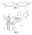
- FIG. 1is a schematic representation of an in situ ruthenium tetraoxide (RuO 4 ) generator of a type usefully employed in the ALD systems and processes of the invention.
- RuO 4ruthenium tetraoxide
- FIG. 2is a schematic representation of an ALD process system incorporating a ruthenium tetraoxide in situ generation system according to one embodiment of the invention.
- FIG. 3is a schematic representation of a container useful in generating ruthenium tetraoxide, according to one specific embodiment of the invention.
- FIG. 4is a schematic process diagram of a process for generating ruthenium tetraoxide, vapor depositing a strontium ruthenate electrode on a microelectronic device substrate, in the manufacture of a high k dielectric capacitor device, and abating ruthenate-containing effluent from the vapor depositing operation.
- the present inventionrelates to use of ruthenium tetraoxide as a precursor for vapor deposition of ruthenium-containing films, e.g., in the manufacture of high k capacitor devices, wherein the ruthenium tetraoxide precursor is generated in situ and flowed from the location of generation to a vapor deposition apparatus in which the ruthenium tetraoxide precursor vapor is contacted under vapor deposition conditions with a microelectronic device substrate, such as a silicon wafer, or other semiconductor substrate.
- a microelectronic device substratesuch as a silicon wafer, or other semiconductor substrate.
- the inventionrelates to an atomic layer deposition method for forming a strontium ruthenate film on a substrate, e.g., in the manufacture of a high k dielectric material capacitor on a microelectronic device substrate.
- the inventionalso contemplates apparatus and method for abatement of a ruthenate-containing effluent from a ruthenium-containing film formation process, in which the effluent from the deposition of the ruthenium-containing film is contacted with an abatement composition comprising an acid, or a base, or other recovery medium, for recovery of ruthenium.
- the inventionprovides an efficient and economic apparatus and method for forming Ru and SrRuO 3 electrodes, e.g., in the fabrication of DRAM capacitors.
- the inventionachieves a major advance over the use of metal organic precursors for vapor deposition of ruthenium.
- metal organic precursorshave the disadvantages of long incubation times, produce rough films that also incorporate significant levels of carbon and oxygen, and realize only low utilization levels of precursor, e.g., 10 grams precursor per wafer.
- the present inventionby using RuO 4 as a precursor for vapor deposition of ruthenium-containing films on microelectronic device substrates, provides a highly volatile precursor that produces extremely smooth films with no carbon incorporation in the film.
- the inventionalso resolves safety and performance issues related to the toxicity of RuO 4 and the inability to store it in a pressurized vessel because of its instability under long-term storage conditions and susceptibility to explosive hazard.
- the inventionutilizes the approach of generating RuO 4 on demand, at the point of use from Ru and/or RuO 2 both of which are very stable and non-toxic solids.
- the RuO 4is generated by reaction with an oxic gas, such as ozone, oxygen, nitrogen oxide, singlet oxygen, air, or other oxic (oxygen-containing) gas.
- an oxic gassuch as ozone, oxygen, nitrogen oxide, singlet oxygen, air, or other oxic (oxygen-containing) gas.
- the RuO 4is contacted with the microelectronic device substrate, resulting in efficient formation of ruthenium-containing films, such as films of elemental Ru or RuO 2 , and any effluent containing RuO 4 , RuO 2 , and unreacted oxic gas is readily abated by scrubbing the effluent gas with dilute acid or other suitable scrubbing medium.
- the effluent waste resulting from the abatementcan be collected for refining of Ru metal to further enhance the
- RuO 4thus can be generated only when needed, as a reaction product produced by reaction of the ruthenium starting material, comprising Ru and/or RuO 2 , with the oxic gas.
- the ruthenium starting materialcan be provided in a storage and dispensing vessel through which the oxic gas is flowed for contact with the ruthenium starting material, to produce RuO 4 as a reaction product gas that can be discharged from the storage and dispensing vessel at a desired rate, by use of a flow control valve, mass flow controller, restricted flow orifice, or other flow control element(s) and/or flow circuitry
- the RuO 4 subsequent to generation at the point of useis contacted with a microelectronic device substrate, e.g., a silicon wafer or other microelectronic device precursor structure under vapor deposition conditions, so that a ruthenium material comprising elemental ruthenium and/or ruthenium dioxide is deposited on the surface of the substrate.
- a microelectronic device substratee.g., a silicon wafer or other microelectronic device precursor structure under vapor deposition conditions, so that a ruthenium material comprising elemental ruthenium and/or ruthenium dioxide is deposited on the surface of the substrate.
- atomic layer depositionis carried out using RuO 4 and a strontium organo-metallic precursor, such as Sr( n PrMe 4 Cp) 2 , Sr(EtMe 4 Cp) 2 , Sr(thd) 2 , or Sr(thd) 2 .
- a strontium organo-metallic precursorsuch as Sr( n PrMe 4 Cp) 2 , Sr(EtMe 4 Cp) 2 , Sr(thd) 2 , or Sr(thd) 2 .
- PMDETAinvolving pulsing of the Sr precursor into the ALD deposition chamber for strontium oxide deposition on the substrate surface, following which excess Sr precursor is purged from the deposition chamber, and RuO 4 and O 3 (or other oxic gas) are pulsed into the deposition chamber.
- the RuO 4 and O 3thereby serve as oxidant and ruthenium deposition source materials.
- the deposition chamberis purged of the RuO 4 , and the aforementioned steps of ruthenium precursor contacting and strontium precursor contacting then are carried out alternatingly and repetitively in sequence, to form a SrRuO 3 film on the substrate.
- RuO 4is a very volatile and small molecule, which easily penetrates into deep trenches in the microelectronic device substrate.
- ozone (O 3 ) as the oxic gasis highly beneficial in stabilizing the RuO 4 to avoid its premature decomposition, with oxygen and ozone both reacting with RuO 2 to form RuO 4 by the following reactions:
- RuO 4can be used as a chemical vapor deposition precursor to deposit Ru or RuO 2 films.
- RuO 4can be used as an oxidant to react with ruthenium metal organic precursors, e.g., ruthenium cyclopentadienyls such as (Et(Cp) 2 Ru and/or or ruthenium ⁇ -diketonates such as Ru(thd) 3 , wherein Cp is cyclopentadienyl, Et is ethyl, and thd is 2,2,6,6-tetramethyl-3,5-heptanedionate, to form ruthenium thin films.
- ruthenium metal organic precursorse.g., ruthenium cyclopentadienyls such as (Et(Cp) 2 Ru and/or or ruthenium ⁇ -diketonates such as Ru(thd) 3 , wherein Cp is cyclopentadienyl, Et is ethyl,
- RuO 4decomposes rapidly when it is mixed with dilute acid, such as HCl, or a base.
- the effluent waste resulting from the ruthenium film formation processes of the inventiontherefore can be readily treated by contacting with dilute acid, to recover and recycle Ru metal, e.g., for using in fabricating electrodes in DRAM applications.
- DRAM devicescan be formed with electrodes of ruthenium or ruthenium oxide by vapor deposition processes of the present invention, to form capacitor structures based on high k dielectric materials such as strontium titanate (STO) and barium strontium titanate (BST).
- STOstrontium titanate
- BSTbarium strontium titanate
- RuO 4is a yellow highly viscous liquid at room temperature (26-30° C.), having a boiling point of 130° C., a melting point of 25.4° C. and a vapor pressure of 10 torr at 25° C. It is a strong oxidant to organics.
- FIG. 1is a schematic representation of an in situ ruthenium tetraoxide (RuO 4 ) generator of a type usefully employed in the ALD systems and processes of the invention. As illustrated, a vessel is provided that holds Ru and/or RuO 2 source material, and ozone or other oxic gas is flowed through the vessel, to generate RuO 4 .
- RuO 4ruthenium tetraoxide
- RuO 4thus can be generated for use in CVD and/or ALD applications using a vessel holding the Ru and/or RuO 2 source material.
- the source materialmay be in any suitable form, such as a powder, porous block, deposited layer of source material, or other appropriate form.
- the ruthenium source materialis provided in a porous, foamed, or powder form in a vessel such as a Pro-EvapTM solid source vaporizer, commercially available from ATMI, Inc. (Danbury, Conn., USA).
- Oxygen or ozone with inert gas(es)is passed through the vessel at elevated temperature, e.g., a temperature in a range of from 40° C. to 400° C., to form RuO 4 .
- the ruthenium tetraoxide resulting from the reaction of Ru or RuO 2 and the ozone/oxygen gasis flowed from the vessel to a deposition chamber, such as an ALD chamber, for deposition of Ru thin film, or Ru-containing materials such as strontium ruthenate (SRO), when a strontium source is also employed in the deposition process.
- a deposition chambersuch as an ALD chamber
- Ru-containing materialssuch as strontium ruthenate (SRO)
- FIG. 2is a schematic representation of an ALD process system 10 incorporating a ruthenium tetraoxide in situ generation system according to one embodiment of the invention.
- the system 10includes an in situ generator 12 for producing ruthenium tetraoxide, a strontium precursor source 50 , an atomic layer deposition apparatus 100 , and an effluent abatement apparatus 200 for abating the ruthenium-containing output resulting from the ALD process to produce a ruthenium-reduced effluent.
- the in situ generator 12includes a storage and dispensing vessel 14 such as a conventional gas cylinder container holding a ruthenium tetraoxide precursor 15 , such as elemental ruthenium or ruthenium dioxide.
- a ruthenium tetraoxide precursor 15such as elemental ruthenium or ruthenium dioxide.
- the precursor 15is constituted by a ruthenium metal foam in the interior volume 16 of the vessel.
- the vesselincludes a valve head 18 containing a valve (not shown) that is actuated by the hand wheel 20 , or by an automatic valve actuator, to open or close the container to flow.
- a feed conduit 30Joined to the valve head 18 is a feed conduit 30 that communicates with the valve head inlet 22 through an inlet passage in the valve head, and terminates at a lower end in the lower portion of the vessel 14 .
- the valve headalso includes an outlet 24 that communicates with a discharge conduit 32 terminating at a lower end in an upper portion of the interior volume 16 of the vessel 14 .
- oxic gasis enabled to flow from inlet 22 through the valve head 18 into the feed conduit 30 for discharge in the lower portion of the vessel and flow upwardly through the ruthenium tetraoxide precursor for reaction to form the ruthenium tetraoxide.
- the resulting ruthenium oxidethen flows through the discharge conduit 32 through the valve head to outlet 24 , for dispensing from the vessel.
- the vessel 14is circumscribed along its length by a heating coil 19 that may be energized by a suitable power supply (not shown).
- the vesselmay be equipped with a heating jacket, disposed in a heating bath, have heating coils embedded in the vessel wall, or otherwise be adapted for heating of the vessel to temperature in a range of from 40° C. to 400° C.
- the system 10includes an oxic gas source 26 , which may for example comprise an oxygen cylinder, compressed air supply, ozone generator, or other suitable source of oxic gas for the system.
- the oxic gas source 26is coupled by feed line 28 with the inlet 22 of the container holding the ruthenium tetraoxide precursor.
- the system 10also includes a vapor delivery line 34 connected with inlet 36 of vapor deposition apparatus comprising an atomic layer deposition apparatus 100 .
- the ALD apparatus 100includes an ALD deposition chamber 40 enclosing an interior volume 62 in which it is mounted in a showerhead disperser 38 communicating with inlet 36 for discharge of vapor. From the showerhead, the vapor is impinged on a microelectronic device substrate 46 to form a ruthenium-containing film 48 thereon.
- the microelectronic device substrate 46is mounted on susceptor 42 , which is heated by an embedded coil 44 to appropriate temperature for the atomic layer deposition operation.
- a strontium precursor source 50comprising a precursor storage and dispensing vessel 52 with valve head 54 to which is coupled with hand wheel 56 to control the valve in the valve head.
- the valve headhas an outlet 58 coupled to feed line 64 delivery of strontium precursor from vessel 52 to the inlet 36 of the ALD apparatus 100 .
- An effluent discharge line 64is coupled to ALD chamber 40 , for discharge of effluent from the ALD process to the effluent abatement apparatus 200 .
- Such apparatusmay comprise a scrubbing apparatus 66 in which the ruthenium-containing effluent resulting from the ALD operation in chamber 40 is scrubbed with an acidic medium for treatment of the effluent to produce a ruthenium-reduced effluent that is discharged from the scrubbing apparatus 66 in discharge line 68 , for venting to the atmosphere, or other treatment or disposition.
- the ruthenium oxides in the ruthenium-containing effluentare scrubbed to recover ruthenium.
- Such recovered rutheniumthat can be processed for reuse in the system, thereby lowering the capital and operating costs of the system.
- ruthenium precursor and strontium precursor from the respective sourcesare sequentially and alternatingly contacted with the microelectronic device substrate to form a strontium ruthenate (SrRuO 3 ) film on the substrate.
- the ALD processcan be carried out in any suitable manner that is effective to deposit the ruthenium and strontium material on the substrate.
- a cylinder-type containermay be packed with porous Ru metal or RuO 2 , with oxygen or ozone being passed through the container at elevated temperature to generate RuO 4 for the ALD formation of an SRO electrode, as described above.
- the respective RuO 4 and organometallic Sr precursorsare then alternatingly and repetitively contacted with the microelectronic device substrate for as many repetitive cycles as necessary to form a SrRuO 3 film of predetermined thickness.
- the process conditions for deposition of Ru-containing films in accordance with the inventionmay be carried out at any suitable temperature, pressure, flow rate and other process conditions, as necessary or desirable to form an Ru-containing film of appropriate character for a specific application, as is readily determinable within the skill of the art based on the disclosure herein.
- the apparatus of the inventionmay be configured in a wide variety of arrangements, for the vapor phase deposition of ruthenium within the broad scope of the invention.
- the apparatusis configured as a system for manufacturing a microelectronic device, comprising:
- a container holding at least one RuO 4 precursor selected from among Ru and RuO 2such container being adapted for heating to temperature in a range of from 40° C. to 400° C., having an inlet for introducing an oxic gas into the container for reaction with the RuO 4 precursor to form gaseous RuO 4 and having an outlet for flowing gaseous RuO 4 out of the container;
- Such systemmay further include a heater arranged to heat the container to the desired temperature.
- the oxic gas supplycan supply an oxic gas such as oxygen, ozone, air, or nitrogen oxide.
- the oxic gasis ozone, and the oxic gas supply comprises an ozone generator.
- the semiconductor manufacturing vapor deposition tool that is employedcan be of any suitable type, and can include a chemical vapor deposition apparatus, or alternatively an atomic layer deposition apparatus.
- the atomic layer deposition apparatusmay as indicated be arranged to flow a strontium precursor from a strontium precursor source to the apparatus, for depositing a strontium ruthenium oxide film on a microelectronic device substrate.
- Such strontium ruthenium oxide filmmay define a SrRuO 3 electrode structure on the microelectronic device substrate.
- the container employed to supply the ruthenium tetraoxidecan be of any suitable type, and may for example include support surface elements in the interior volume of such container, in contact with the ruthenium tetraoxide precursor.
- the support surface elementsmay include plates, shelves, trays or other internal support surface elements, in contact with the RuO 4 precursor.
- the support surface elementsmay comprise an array of trays on which the precursor is reposed on the tray surfaces.
- the ruthenium tetroxide precursormay be present in the container in the form of a porous foam material.
- the vapor deposition chambercan be coupled in a relationship with an abatement tool, such as a scrubber, catalytic oxidizer, chemisorbent unit, physical adsorbent system or other abatement apparatus unsuitable character to treat the effluent for reduction and/or recovery of ruthenium therein, to produce a ruthenium-reduced effluent.
- a scrubber apparatusmay be arranged to contact the effluent from the vapor deposition tool with an acidic scrubbing medium such as the HCl or other scrubbing agent effective to reduce ruthenium in said effluent.
- the inventionus provides a method of manufacturing a microelectronic device, comprising:
- the contactingmay comprise chemical vapor deposition, atomic layer deposition, or other vapor deposition operation.
- the contactingin a specific embodiment may comprise contacting the microelectronic device substrate with a strontium-containing precursor vapor, e.g., SrO 2 , alternatingly and repetitively with such contacting of the microelectronic device substrate with the gaseous RuO 4 , so as to form a strontium- and ruthenium-containing film on the microelectronic device substrate.
- a strontium-containing precursor vapore.g., SrO 2
- a SrRuO 3 filmcan be formed that is extremely smooth in character, and free of the presence of carbon.
- Such filmis suitable for forming an electrode of a capacitor on the microelectronic device substrate.
- Such capacitormay comprise a high k dielectric material, such as barium titanate or barium strontium titanate, in a DRAM device.
- the inventionalso contemplates a ruthenium tetraoxide supply apparatus, comprising a container holding at least one RuO 4 precursor selected from among Ru and RuO 2 , such container being adapted for heating to temperature in a range of from 40° C. to 400° C., having an inlet for introducing an oxic gas into said container for reaction with the RuO 4 precursor to form gaseous RuO 4 and having an outlet for flowing gaseous RuO 4 out of the container.
- the apparatusmay further comprise a heater adapted to heat the container to the aforementioned temperature in the range from 40° C. to 400° C.
- Such ruthenium tetraoxide supply apparatusmay further include an oxic gas source coupled with the container and arranged for flow of oxic gas from an oxic gas source through the container, for contacting with the ruthenium tetraoxide precursor therein.
- an oxic gas sourcecoupled with the container and arranged for flow of oxic gas from an oxic gas source through the container, for contacting with the ruthenium tetraoxide precursor therein.
- FIG. 3is a schematic representation of a container 310 useful in generating ruthenium tetraoxide, according to one specific embodiment of the invention.
- the containerincludes a vessel 312 , fabricated of a suitable heat-conducting material, such as for example silver, silver alloys, copper, copper alloys, aluminum, aluminum alloys, lead, nickel clad, stainless steel, graphite and/or ceramic material.
- the vesselcomprises a bottom 314 and sidewall 316 forming an internal compartment.
- the vesselcan be any shape that facilitates an even flow of oxic gas through the vessel, such as the illustrated cylindrical shape.
- the preferred shape of the vessel baseis a cylindrical shape machined to very tight tolerances.
- the containeris fabricated to ensure that each side wall of the internal trays has good thermal contact with the interior walls of the vessel.
- Oxic gas inlet 320is preferably positioned on the vessel top 318 and communicatively connected to the vessel for introducing the oxic gas into the vessel.
- a plurality of vertically stacked trays 322Positioned within the internal compartment of the vessel is a plurality of vertically stacked trays 322 . The stacked trays are separable from each other and removable from the vessel for easy cleaning and refilling.
- an internal oxic gas member 323Positioned within the vessel is an internal oxic gas member 323 that is connected (welded) to the gas inlet 320 and directs the oxic gas to the bottom of the internal compartment and below the lowest tray in the array of vertically stacked trays. The internal oxic gas member 323 passes through each tray cavity and tray bottom.
- a sealing O-ring(not shown) may be positioned between trays.
- An addition of an outer o-ringis also contemplated to seal between trays on the top surface of each tray sidewall.
- the containerin order to prevent entrainment of solids in the gas flow through the container, by use of appropriate frit or filter elements in the gas flow path.
- the ruthenium tetraoxide precursor material in the containermay be coated in the form of a film on one or more of the support surfaces of the stacked trays in the FIG. 3 .
- Such filmmay be applied by melting the ruthenium precursor, applying it over one or more of the support surfaces of the trays, followed by cooling to solidify the material in a layer on the surface of the trays.
- a solvent solution of the ruthenium tetraoxide precursorcan be applied over one or more support surfaces of respective trays, followed by removal of the solvent to leave a deposit film of the ruthenium precursor on the surface of the trays.
- One commercially available stacked tray container amenable for use for in situ generation of ruthenium tetraoxide in accordance with the present inventionis the Pro-EvapTM vapor delivery vessel, available from ATMI, Inc. (Danbury, Conn., USA).
- FIG. 4is a schematic process diagram of a process for generating ruthenium tetraoxide, vapor depositing a strontium ruthenate electrode on a microelectronic device substrate for manufacture of a high k dielectric capacitor device, and abating ruthenium-containing effluent from the vapor depositing operation.
- ruthenium tetraoxideis generated by reaction of ruthenium or ruthenium dioxide with oxic gas, e.g., ozone, flowed through a source vessel containing ruthenium or ruthenium dioxide.
- oxic gase.g., ozone
- the ruthenium tetraoxide vaporis flowed to an atomic layer deposition chamber and contacted with a wafer therein.
- strontium precursor vaporis flowed to the atomic layer deposition chamber and deposited on the ruthenium layer on the wafer.
- the steps of ruthenium tetraoxide vapor and strontium precursor vapor contactingthen are repeated a desired number of times in sequence, to deposit a strontium ruthenate electrode on the substrate in the manufacture of a microelectronic device such as a high dielectric constant capacitor.
Landscapes
- Engineering & Computer Science (AREA)
- Chemical & Material Sciences (AREA)
- Power Engineering (AREA)
- Microelectronics & Electronic Packaging (AREA)
- Manufacturing & Machinery (AREA)
- General Chemical & Material Sciences (AREA)
- Chemical Kinetics & Catalysis (AREA)
- Condensed Matter Physics & Semiconductors (AREA)
- Computer Hardware Design (AREA)
- Materials Engineering (AREA)
- General Physics & Mathematics (AREA)
- Physics & Mathematics (AREA)
- Mechanical Engineering (AREA)
- Metallurgy (AREA)
- Organic Chemistry (AREA)
- Inorganic Chemistry (AREA)
- Ceramic Engineering (AREA)
- Electrochemistry (AREA)
- Chemical Vapour Deposition (AREA)
Abstract
Description
- This application claims the benefit of priority under the provisions of 35 USC §119 of U.S. Provisional Patent Application No. 61/152,604 filed Feb. 13, 2009. The disclosure of such U.S. Provisional Patent Application No. 61/152,604 is hereby incorporated herein by reference in its respective entirety, for all purposes.
- The present invention relates to apparatus and method for in situ generation of ruthenium tetraoxide (RuO4) for use in vapor deposition, e.g., atomic layer deposition (ALD), of ruthenium-containing films in the manufacture of microelectronic devices such as high k dielectric material capacitors having ruthenium-containing electrode(s).
- Ruthenium (Ru) and Group II metal ruthenates such as strontium ruthenate (SrRuO3) are promising electrode materials for high k capacitor applications. Smooth thin layers of Ru metal films can also be employed as seed layers or barrier layers for Cu electroplating in copper metallization processes.
- ALD is often used as a technique to deposit Ru and Ru-containing thin films to achieve superior step coverage in high aspect ratio structures. For such purpose, metal organic precursors, e.g., ruthenium cyclopentadienyls or ruthenium β-diketonates such as (Et(Cp)2Ru and Ru(thd)3, wherein Cp is cyclopentadienyl, Et is ethyl, and thd is 2,2,6,6-tetramethyl-3,5-heptanedionate, are commonly used. These precursors, however, require long incubation times and frequently produce deposited films that are very rough in texture.
- The art therefore continues to seek improved ruthenium precursors for vapor deposition processes to form ruthenium-containing thin films without the long incubation times and rough films characteristic of the use of metal organic ruthenium precursors of the prior art.
- The present invention relates to apparatus and method for generating ruthenium tetraoxide on demand for use in manufacturing semiconductor or other microelectronic devices.
- In one aspect, the invention relates to a system for manufacturing a microelectronic device, comprising:
- (A) a ruthenium tetraoxide (RuO4) source, adapted for in situ generation of RuO4, said source including:
- (i) an oxic gas supply; and
- (ii) a container holding at least one RuO4precursor selected from among Ru and RuO2, said container being adapted for heating to temperature in a range of from 40° C. to 400° C., having an inlet for introducing an oxic gas into said container for reaction with said RuO4precursor to form gaseous RuO4and having an outlet for flowing gaseous RuO4out of the container; and
- (B) a semiconductor manufacturing vapor deposition tool arranged to receive gaseous RuO4discharged from such container through said outlet, and to effect contacting of said gaseous RuO4with a microelectronic device substrate to deposit Ru and/or RuO2thereon.
- Another aspect of the invention relates to a method of manufacturing a microelectronic device, comprising:
- providing at least one RuO4precursor selected from among Ru and RuO2;
- contacting the RuO4precursor with an oxic gas at temperature temperature in a range of from 40° C. to 400° C. to form gaseous RuO4; and
- contacting the gaseous RuO4with a microelectronic device substrate under vapor deposition conditions to deposit Ru and/or RuO2thereon.
- A further aspect of the invention relates to a ruthenium tetraoxide supply apparatus, comprising a container holding at least one RuO4precursor selected from among Ru and RuO2, said container being adapted for heating to temperature in a range of from 40° C. to 400° C., having an inlet for introducing an oxic gas into said container for reaction with said RuO4precursor to form gaseous RuO4and having an outlet for flowing gaseous RuO4out of the container.
- Other aspects, features and embodiments of the invention will be more fully apparent from the ensuing disclosure and appended claims.
FIG. 1 is a schematic representation of an in situ ruthenium tetraoxide (RuO4) generator of a type usefully employed in the ALD systems and processes of the invention.FIG. 2 is a schematic representation of an ALD process system incorporating a ruthenium tetraoxide in situ generation system according to one embodiment of the invention.FIG. 3 is a schematic representation of a container useful in generating ruthenium tetraoxide, according to one specific embodiment of the invention.FIG. 4 is a schematic process diagram of a process for generating ruthenium tetraoxide, vapor depositing a strontium ruthenate electrode on a microelectronic device substrate, in the manufacture of a high k dielectric capacitor device, and abating ruthenate-containing effluent from the vapor depositing operation.- The present invention relates to use of ruthenium tetraoxide as a precursor for vapor deposition of ruthenium-containing films, e.g., in the manufacture of high k capacitor devices, wherein the ruthenium tetraoxide precursor is generated in situ and flowed from the location of generation to a vapor deposition apparatus in which the ruthenium tetraoxide precursor vapor is contacted under vapor deposition conditions with a microelectronic device substrate, such as a silicon wafer, or other semiconductor substrate.
- In a specific embodiment, the invention relates to an atomic layer deposition method for forming a strontium ruthenate film on a substrate, e.g., in the manufacture of a high k dielectric material capacitor on a microelectronic device substrate.
- The invention also contemplates apparatus and method for abatement of a ruthenate-containing effluent from a ruthenium-containing film formation process, in which the effluent from the deposition of the ruthenium-containing film is contacted with an abatement composition comprising an acid, or a base, or other recovery medium, for recovery of ruthenium.
- The invention provides an efficient and economic apparatus and method for forming Ru and SrRuO3electrodes, e.g., in the fabrication of DRAM capacitors.
- The invention achieves a major advance over the use of metal organic precursors for vapor deposition of ruthenium. Such metal organic precursors have the disadvantages of long incubation times, produce rough films that also incorporate significant levels of carbon and oxygen, and realize only low utilization levels of precursor, e.g., 10 grams precursor per wafer. The present invention by using RuO4as a precursor for vapor deposition of ruthenium-containing films on microelectronic device substrates, provides a highly volatile precursor that produces extremely smooth films with no carbon incorporation in the film. The invention also resolves safety and performance issues related to the toxicity of RuO4and the inability to store it in a pressurized vessel because of its instability under long-term storage conditions and susceptibility to explosive hazard.
- The invention utilizes the approach of generating RuO4on demand, at the point of use from Ru and/or RuO2both of which are very stable and non-toxic solids. The RuO4is generated by reaction with an oxic gas, such as ozone, oxygen, nitrogen oxide, singlet oxygen, air, or other oxic (oxygen-containing) gas. Once generated, the RuO4is contacted with the microelectronic device substrate, resulting in efficient formation of ruthenium-containing films, such as films of elemental Ru or RuO2, and any effluent containing RuO4, RuO2, and unreacted oxic gas is readily abated by scrubbing the effluent gas with dilute acid or other suitable scrubbing medium. The effluent waste resulting from the abatement can be collected for refining of Ru metal to further enhance the economics of the process.
- RuO4thus can be generated only when needed, as a reaction product produced by reaction of the ruthenium starting material, comprising Ru and/or RuO2, with the oxic gas. For such purpose, the ruthenium starting material can be provided in a storage and dispensing vessel through which the oxic gas is flowed for contact with the ruthenium starting material, to produce RuO4as a reaction product gas that can be discharged from the storage and dispensing vessel at a desired rate, by use of a flow control valve, mass flow controller, restricted flow orifice, or other flow control element(s) and/or flow circuitry
- The RuO4subsequent to generation at the point of use, is contacted with a microelectronic device substrate, e.g., a silicon wafer or other microelectronic device precursor structure under vapor deposition conditions, so that a ruthenium material comprising elemental ruthenium and/or ruthenium dioxide is deposited on the surface of the substrate.
- In one preferred aspect of the invention, atomic layer deposition (ALD) is carried out using RuO4and a strontium organo-metallic precursor, such as Sr(nPrMe4Cp)2, Sr(EtMe4Cp)2, Sr(thd)2, or Sr(thd)2.PMDETA, involving pulsing of the Sr precursor into the ALD deposition chamber for strontium oxide deposition on the substrate surface, following which excess Sr precursor is purged from the deposition chamber, and RuO4and O3(or other oxic gas) are pulsed into the deposition chamber. The RuO4and O3thereby serve as oxidant and ruthenium deposition source materials. After contact with the substrate surface by the RuO4and O3, the deposition chamber is purged of the RuO4, and the aforementioned steps of ruthenium precursor contacting and strontium precursor contacting then are carried out alternatingly and repetitively in sequence, to form a SrRuO3film on the substrate.
- RuO4is a very volatile and small molecule, which easily penetrates into deep trenches in the microelectronic device substrate. The presence of ozone (O3) as the oxic gas is highly beneficial in stabilizing the RuO4to avoid its premature decomposition, with oxygen and ozone both reacting with RuO2to form RuO4by the following reactions:
- RuO4can be used as a chemical vapor deposition precursor to deposit Ru or RuO2films. In addition, RuO4can be used as an oxidant to react with ruthenium metal organic precursors, e.g., ruthenium cyclopentadienyls such as (Et(Cp)2Ru and/or or ruthenium β-diketonates such as Ru(thd)3, wherein Cp is cyclopentadienyl, Et is ethyl, and thd is 2,2,6,6-tetramethyl-3,5-heptanedionate, to form ruthenium thin films. As used herein, a thin film is a film having a thickness not exceeding 1 micrometer, such as in a range of from 2 to 1000 nanometers.
- Concerning abatement of effluent from the ruthenium film deposition processes of the invention, RuO4decomposes rapidly when it is mixed with dilute acid, such as HCl, or a base. The effluent waste resulting from the ruthenium film formation processes of the invention therefore can be readily treated by contacting with dilute acid, to recover and recycle Ru metal, e.g., for using in fabricating electrodes in DRAM applications.
- DRAM devices can be formed with electrodes of ruthenium or ruthenium oxide by vapor deposition processes of the present invention, to form capacitor structures based on high k dielectric materials such as strontium titanate (STO) and barium strontium titanate (BST).
- RuO4is a yellow highly viscous liquid at room temperature (26-30° C.), having a boiling point of 130° C., a melting point of 25.4° C. and a vapor pressure of 10 torr at 25° C. It is a strong oxidant to organics.
FIG. 1 is a schematic representation of an in situ ruthenium tetraoxide (RuO4) generator of a type usefully employed in the ALD systems and processes of the invention. As illustrated, a vessel is provided that holds Ru and/or RuO2source material, and ozone or other oxic gas is flowed through the vessel, to generate RuO4.- RuO4thus can be generated for use in CVD and/or ALD applications using a vessel holding the Ru and/or RuO2source material. The source material may be in any suitable form, such as a powder, porous block, deposited layer of source material, or other appropriate form. In one embodiment, the ruthenium source material is provided in a porous, foamed, or powder form in a vessel such as a Pro-Evap™ solid source vaporizer, commercially available from ATMI, Inc. (Danbury, Conn., USA). Oxygen or ozone with inert gas(es) is passed through the vessel at elevated temperature, e.g., a temperature in a range of from 40° C. to 400° C., to form RuO4. The ruthenium tetraoxide resulting from the reaction of Ru or RuO2and the ozone/oxygen gas is flowed from the vessel to a deposition chamber, such as an ALD chamber, for deposition of Ru thin film, or Ru-containing materials such as strontium ruthenate (SRO), when a strontium source is also employed in the deposition process.
FIG. 2 is a schematic representation of anALD process system 10 incorporating a ruthenium tetraoxide in situ generation system according to one embodiment of the invention.- As illustrated, the
system 10 includes an insitu generator 12 for producing ruthenium tetraoxide, astrontium precursor source 50, an atomiclayer deposition apparatus 100, and aneffluent abatement apparatus 200 for abating the ruthenium-containing output resulting from the ALD process to produce a ruthenium-reduced effluent. - The in
situ generator 12 includes a storage and dispensingvessel 14 such as a conventional gas cylinder container holding aruthenium tetraoxide precursor 15, such as elemental ruthenium or ruthenium dioxide. In the embodiment shown, theprecursor 15 is constituted by a ruthenium metal foam in theinterior volume 16 of the vessel. - The vessel includes a
valve head 18 containing a valve (not shown) that is actuated by thehand wheel 20, or by an automatic valve actuator, to open or close the container to flow. Joined to thevalve head 18 is afeed conduit 30 that communicates with thevalve head inlet 22 through an inlet passage in the valve head, and terminates at a lower end in the lower portion of thevessel 14. The valve head also includes anoutlet 24 that communicates with adischarge conduit 32 terminating at a lower end in an upper portion of theinterior volume 16 of thevessel 14. - By such arrangement, oxic gas is enabled to flow from
inlet 22 through thevalve head 18 into thefeed conduit 30 for discharge in the lower portion of the vessel and flow upwardly through the ruthenium tetraoxide precursor for reaction to form the ruthenium tetraoxide. The resulting ruthenium oxide then flows through thedischarge conduit 32 through the valve head tooutlet 24, for dispensing from the vessel. - As illustrated, the
vessel 14 is circumscribed along its length by aheating coil 19 that may be energized by a suitable power supply (not shown). Alternately, the vessel may be equipped with a heating jacket, disposed in a heating bath, have heating coils embedded in the vessel wall, or otherwise be adapted for heating of the vessel to temperature in a range of from 40° C. to 400° C. - The
system 10 includes anoxic gas source 26, which may for example comprise an oxygen cylinder, compressed air supply, ozone generator, or other suitable source of oxic gas for the system. Theoxic gas source 26 is coupled byfeed line 28 with theinlet 22 of the container holding the ruthenium tetraoxide precursor. - The
system 10 also includes avapor delivery line 34 connected withinlet 36 of vapor deposition apparatus comprising an atomiclayer deposition apparatus 100. TheALD apparatus 100 includes anALD deposition chamber 40 enclosing aninterior volume 62 in which it is mounted in ashowerhead disperser 38 communicating withinlet 36 for discharge of vapor. From the showerhead, the vapor is impinged on amicroelectronic device substrate 46 to form a ruthenium-containingfilm 48 thereon. Themicroelectronic device substrate 46 is mounted onsusceptor 42, which is heated by an embeddedcoil 44 to appropriate temperature for the atomic layer deposition operation. - Further included in the
system 10 is astrontium precursor source 50, comprising a precursor storage and dispensingvessel 52 withvalve head 54 to which is coupled withhand wheel 56 to control the valve in the valve head. The valve head has anoutlet 58 coupled to feedline 64 delivery of strontium precursor fromvessel 52 to theinlet 36 of theALD apparatus 100. - An
effluent discharge line 64 is coupled toALD chamber 40, for discharge of effluent from the ALD process to theeffluent abatement apparatus 200. Such apparatus may comprise ascrubbing apparatus 66 in which the ruthenium-containing effluent resulting from the ALD operation inchamber 40 is scrubbed with an acidic medium for treatment of the effluent to produce a ruthenium-reduced effluent that is discharged from the scrubbingapparatus 66 indischarge line 68, for venting to the atmosphere, or other treatment or disposition. - By such treatment, the ruthenium oxides in the ruthenium-containing effluent are scrubbed to recover ruthenium. Such recovered ruthenium that can be processed for reuse in the system, thereby lowering the capital and operating costs of the system.
- In operation at the
system 10 illustrated inFIG. 2 , ruthenium precursor and strontium precursor from the respective sources are sequentially and alternatingly contacted with the microelectronic device substrate to form a strontium ruthenate (SrRuO3) film on the substrate. - The ALD process can be carried out in any suitable manner that is effective to deposit the ruthenium and strontium material on the substrate.
- For example, a cylinder-type container may be packed with porous Ru metal or RuO2, with oxygen or ozone being passed through the container at elevated temperature to generate RuO4for the ALD formation of an SRO electrode, as described above. An organo strontium precursor can be used that is compatible with the process conditions, e.g., Sr(Cp)2, wherein Cp=cyclopentadienyl, or a Sr(beta-diketonate)2precursor such as Sr(thd)2. The respective RuO4and organometallic Sr precursors are then alternatingly and repetitively contacted with the microelectronic device substrate for as many repetitive cycles as necessary to form a SrRuO3film of predetermined thickness.
- The process conditions for deposition of Ru-containing films in accordance with the invention may be carried out at any suitable temperature, pressure, flow rate and other process conditions, as necessary or desirable to form an Ru-containing film of appropriate character for a specific application, as is readily determinable within the skill of the art based on the disclosure herein.
- It will be appreciated that the apparatus of the invention may be configured in a wide variety of arrangements, for the vapor phase deposition of ruthenium within the broad scope of the invention. In one embodiment, the apparatus is configured as a system for manufacturing a microelectronic device, comprising:
- (A) a ruthenium tetraoxide (RuO4) source, adapted for in situ generation of RuO4, in which the source includes:
- (i) an oxic gas supply; and
- (ii) a container holding at least one RuO4precursor selected from among Ru and RuO2, such container being adapted for heating to temperature in a range of from 40° C. to 400° C., having an inlet for introducing an oxic gas into the container for reaction with the RuO4precursor to form gaseous RuO4and having an outlet for flowing gaseous RuO4out of the container; and
- (B) a semiconductor manufacturing vapor deposition tool arranged to receive gaseous RuO4discharged from such container through the outlet, and to effect contacting of the gaseous RuO4with a microelectronic device substrate to deposit Ru and/or RuO2thereon.
- Such system may further include a heater arranged to heat the container to the desired temperature. The oxic gas supply can supply an oxic gas such as oxygen, ozone, air, or nitrogen oxide. In one specific embodiment, the oxic gas is ozone, and the oxic gas supply comprises an ozone generator.
- The semiconductor manufacturing vapor deposition tool that is employed can be of any suitable type, and can include a chemical vapor deposition apparatus, or alternatively an atomic layer deposition apparatus. The atomic layer deposition apparatus may as indicated be arranged to flow a strontium precursor from a strontium precursor source to the apparatus, for depositing a strontium ruthenium oxide film on a microelectronic device substrate.
- Such strontium ruthenium oxide film may define a SrRuO3electrode structure on the microelectronic device substrate.
- The container employed to supply the ruthenium tetraoxide can be of any suitable type, and may for example include support surface elements in the interior volume of such container, in contact with the ruthenium tetraoxide precursor. The support surface elements may include plates, shelves, trays or other internal support surface elements, in contact with the RuO4precursor. For example, the support surface elements may comprise an array of trays on which the precursor is reposed on the tray surfaces.
- Alternatively, the ruthenium tetroxide precursor may be present in the container in the form of a porous foam material.
- The vapor deposition chamber can be coupled in a relationship with an abatement tool, such as a scrubber, catalytic oxidizer, chemisorbent unit, physical adsorbent system or other abatement apparatus unsuitable character to treat the effluent for reduction and/or recovery of ruthenium therein, to produce a ruthenium-reduced effluent. For example, a scrubber apparatus may be arranged to contact the effluent from the vapor deposition tool with an acidic scrubbing medium such as the HCl or other scrubbing agent effective to reduce ruthenium in said effluent.
- The invention us provides a method of manufacturing a microelectronic device, comprising:
- providing at least one RuO4precursor selected from among Ru and RuO2;
- contacting the RuO4precursor with an oxic gas, e.g., oxygen, ozone, air, nitrogen oxide, etc., at temperature temperature in a range of from 40° C. to 400° C. to form gaseous RuO4; and
- contacting the gaseous RuO4with a microelectronic device substrate under vapor deposition conditions to deposit Ru and/or RuO2thereon.
- The contacting may comprise chemical vapor deposition, atomic layer deposition, or other vapor deposition operation. The contacting in a specific embodiment may comprise contacting the microelectronic device substrate with a strontium-containing precursor vapor, e.g., SrO2, alternatingly and repetitively with such contacting of the microelectronic device substrate with the gaseous RuO4, so as to form a strontium- and ruthenium-containing film on the microelectronic device substrate.
- In such manner, a SrRuO3film can be formed that is extremely smooth in character, and free of the presence of carbon. Such film is suitable for forming an electrode of a capacitor on the microelectronic device substrate. Such capacitor may comprise a high k dielectric material, such as barium titanate or barium strontium titanate, in a DRAM device.
- The invention also contemplates a ruthenium tetraoxide supply apparatus, comprising a container holding at least one RuO4precursor selected from among Ru and RuO2, such container being adapted for heating to temperature in a range of from 40° C. to 400° C., having an inlet for introducing an oxic gas into said container for reaction with the RuO4precursor to form gaseous RuO4and having an outlet for flowing gaseous RuO4out of the container. The apparatus may further comprise a heater adapted to heat the container to the aforementioned temperature in the range from 40° C. to 400° C.
- Such ruthenium tetraoxide supply apparatus may further include an oxic gas source coupled with the container and arranged for flow of oxic gas from an oxic gas source through the container, for contacting with the ruthenium tetraoxide precursor therein.
FIG. 3 is a schematic representation of acontainer 310 useful in generating ruthenium tetraoxide, according to one specific embodiment of the invention. The container includes avessel 312, fabricated of a suitable heat-conducting material, such as for example silver, silver alloys, copper, copper alloys, aluminum, aluminum alloys, lead, nickel clad, stainless steel, graphite and/or ceramic material. The vessel comprises a bottom314 andsidewall 316 forming an internal compartment. The vessel can be any shape that facilitates an even flow of oxic gas through the vessel, such as the illustrated cylindrical shape. The preferred shape of the vessel base is a cylindrical shape machined to very tight tolerances. The container is fabricated to ensure that each side wall of the internal trays has good thermal contact with the interior walls of the vessel.Oxic gas inlet 320 is preferably positioned on thevessel top 318 and communicatively connected to the vessel for introducing the oxic gas into the vessel. Positioned within the internal compartment of the vessel is a plurality of vertically stackedtrays 322. The stacked trays are separable from each other and removable from the vessel for easy cleaning and refilling. Positioned within the vessel is an internaloxic gas member 323 that is connected (welded) to thegas inlet 320 and directs the oxic gas to the bottom of the internal compartment and below the lowest tray in the array of vertically stacked trays. The internaloxic gas member 323 passes through each tray cavity and tray bottom. If necessary to ensure a leak-proof seal at the point where the internal oxic gas member intersects the tray bottom, a sealing O-ring (not shown) may be positioned between trays. An addition of an outer o-ring is also contemplated to seal between trays on the top surface of each tray sidewall.- Depending on the specific form of the ruthenium tetraoxide precursor, it may be desirable to modify the container in order to prevent entrainment of solids in the gas flow through the container, by use of appropriate frit or filter elements in the gas flow path.
- The ruthenium tetraoxide precursor material in the container may be coated in the form of a film on one or more of the support surfaces of the stacked trays in the
FIG. 3 . Such film may be applied by melting the ruthenium precursor, applying it over one or more of the support surfaces of the trays, followed by cooling to solidify the material in a layer on the surface of the trays. Alternatively, a solvent solution of the ruthenium tetraoxide precursor can be applied over one or more support surfaces of respective trays, followed by removal of the solvent to leave a deposit film of the ruthenium precursor on the surface of the trays. - One commercially available stacked tray container amenable for use for in situ generation of ruthenium tetraoxide in accordance with the present invention is the Pro-Evap™ vapor delivery vessel, available from ATMI, Inc. (Danbury, Conn., USA).
FIG. 4 is a schematic process diagram of a process for generating ruthenium tetraoxide, vapor depositing a strontium ruthenate electrode on a microelectronic device substrate for manufacture of a high k dielectric capacitor device, and abating ruthenium-containing effluent from the vapor depositing operation.- In the initial (top) step, ruthenium tetraoxide is generated by reaction of ruthenium or ruthenium dioxide with oxic gas, e.g., ozone, flowed through a source vessel containing ruthenium or ruthenium dioxide.
- In the next step, the ruthenium tetraoxide vapor is flowed to an atomic layer deposition chamber and contacted with a wafer therein.
- Thereafter, strontium precursor vapor is flowed to the atomic layer deposition chamber and deposited on the ruthenium layer on the wafer. The steps of ruthenium tetraoxide vapor and strontium precursor vapor contacting then are repeated a desired number of times in sequence, to deposit a strontium ruthenate electrode on the substrate in the manufacture of a microelectronic device such as a high dielectric constant capacitor.
- While the invention has been has been described herein in reference to specific aspects, features and illustrative embodiments of the invention, it will be appreciated that the utility of the invention is not thus limited, but rather extends to and encompasses numerous other variations, modifications and alternative embodiments, as will suggest themselves to those of ordinary skill in the field of the present invention, based on the disclosure herein. Correspondingly, the invention as hereinafter claimed is intended to be broadly construed and interpreted, as including all such variations, modifications and alternative embodiments, within its spirit and scope.

Claims (20)
Priority Applications (1)
| Application Number | Priority Date | Filing Date | Title |
|---|---|---|---|
| US12/705,587US8663735B2 (en) | 2009-02-13 | 2010-02-13 | In situ generation of RuO4 for ALD of Ru and Ru related materials |
Applications Claiming Priority (2)
| Application Number | Priority Date | Filing Date | Title |
|---|---|---|---|
| US15260409P | 2009-02-13 | 2009-02-13 | |
| US12/705,587US8663735B2 (en) | 2009-02-13 | 2010-02-13 | In situ generation of RuO4 for ALD of Ru and Ru related materials |
Publications (2)
| Publication Number | Publication Date |
|---|---|
| US20100209598A1true US20100209598A1 (en) | 2010-08-19 |
| US8663735B2 US8663735B2 (en) | 2014-03-04 |
Family
ID=42560150
Family Applications (1)
| Application Number | Title | Priority Date | Filing Date |
|---|---|---|---|
| US12/705,587Active2032-09-06US8663735B2 (en) | 2009-02-13 | 2010-02-13 | In situ generation of RuO4 for ALD of Ru and Ru related materials |
Country Status (1)
| Country | Link |
|---|---|
| US (1) | US8663735B2 (en) |
Cited By (322)
| Publication number | Priority date | Publication date | Assignee | Title |
|---|---|---|---|---|
| US20110094385A1 (en)* | 2009-04-16 | 2011-04-28 | Gates Kraig R | Natural Gas Reclaimer Device |
| US20130059078A1 (en)* | 2010-02-23 | 2013-03-07 | Julien Gatineau | Use of ruthenium tetroxide as a precursor and reactant for thin film depositions |
| US20190252195A1 (en)* | 2018-02-14 | 2019-08-15 | Asm Ip Holding B.V. | Method for depositing a ruthenium-containing film on a substrate by a cyclical deposition process |
| US10559458B1 (en) | 2018-11-26 | 2020-02-11 | Asm Ip Holding B.V. | Method of forming oxynitride film |
| US10561975B2 (en) | 2014-10-07 | 2020-02-18 | Asm Ip Holdings B.V. | Variable conductance gas distribution apparatus and method |
| USD876504S1 (en) | 2017-04-03 | 2020-02-25 | Asm Ip Holding B.V. | Exhaust flow control ring for semiconductor deposition apparatus |
| US10590535B2 (en) | 2017-07-26 | 2020-03-17 | Asm Ip Holdings B.V. | Chemical treatment, deposition and/or infiltration apparatus and method for using the same |
| US10600673B2 (en) | 2015-07-07 | 2020-03-24 | Asm Ip Holding B.V. | Magnetic susceptor to baseplate seal |
| US10604847B2 (en) | 2014-03-18 | 2020-03-31 | Asm Ip Holding B.V. | Gas distribution system, reactor including the system, and methods of using the same |
| US10612136B2 (en) | 2018-06-29 | 2020-04-07 | ASM IP Holding, B.V. | Temperature-controlled flange and reactor system including same |
| US10622375B2 (en) | 2016-11-07 | 2020-04-14 | Asm Ip Holding B.V. | Method of processing a substrate and a device manufactured by using the method |
| US10643904B2 (en) | 2016-11-01 | 2020-05-05 | Asm Ip Holdings B.V. | Methods for forming a semiconductor device and related semiconductor device structures |
| US10643826B2 (en) | 2016-10-26 | 2020-05-05 | Asm Ip Holdings B.V. | Methods for thermally calibrating reaction chambers |
| US10655221B2 (en) | 2017-02-09 | 2020-05-19 | Asm Ip Holding B.V. | Method for depositing oxide film by thermal ALD and PEALD |
| US10658181B2 (en) | 2018-02-20 | 2020-05-19 | Asm Ip Holding B.V. | Method of spacer-defined direct patterning in semiconductor fabrication |
| US10658205B2 (en) | 2017-09-28 | 2020-05-19 | Asm Ip Holdings B.V. | Chemical dispensing apparatus and methods for dispensing a chemical to a reaction chamber |
| US10665452B2 (en) | 2016-05-02 | 2020-05-26 | Asm Ip Holdings B.V. | Source/drain performance through conformal solid state doping |
| US10672636B2 (en) | 2017-08-09 | 2020-06-02 | Asm Ip Holding B.V. | Cassette holder assembly for a substrate cassette and holding member for use in such assembly |
| US10685834B2 (en) | 2017-07-05 | 2020-06-16 | Asm Ip Holdings B.V. | Methods for forming a silicon germanium tin layer and related semiconductor device structures |
| US10683571B2 (en) | 2014-02-25 | 2020-06-16 | Asm Ip Holding B.V. | Gas supply manifold and method of supplying gases to chamber using same |
| US10692741B2 (en) | 2017-08-08 | 2020-06-23 | Asm Ip Holdings B.V. | Radiation shield |
| US10707106B2 (en) | 2011-06-06 | 2020-07-07 | Asm Ip Holding B.V. | High-throughput semiconductor-processing apparatus equipped with multiple dual-chamber modules |
| US10714315B2 (en) | 2012-10-12 | 2020-07-14 | Asm Ip Holdings B.V. | Semiconductor reaction chamber showerhead |
| US10714335B2 (en) | 2017-04-25 | 2020-07-14 | Asm Ip Holding B.V. | Method of depositing thin film and method of manufacturing semiconductor device |
| US10714350B2 (en) | 2016-11-01 | 2020-07-14 | ASM IP Holdings, B.V. | Methods for forming a transition metal niobium nitride film on a substrate by atomic layer deposition and related semiconductor device structures |
| US10714385B2 (en) | 2016-07-19 | 2020-07-14 | Asm Ip Holding B.V. | Selective deposition of tungsten |
| US10720331B2 (en) | 2016-11-01 | 2020-07-21 | ASM IP Holdings, B.V. | Methods for forming a transition metal nitride film on a substrate by atomic layer deposition and related semiconductor device structures |
| US10720322B2 (en) | 2016-02-19 | 2020-07-21 | Asm Ip Holding B.V. | Method for forming silicon nitride film selectively on top surface |
| US10734223B2 (en) | 2017-10-10 | 2020-08-04 | Asm Ip Holding B.V. | Method for depositing a metal chalcogenide on a substrate by cyclical deposition |
| US10734244B2 (en) | 2017-11-16 | 2020-08-04 | Asm Ip Holding B.V. | Method of processing a substrate and a device manufactured by the same |
| US10734497B2 (en) | 2017-07-18 | 2020-08-04 | Asm Ip Holding B.V. | Methods for forming a semiconductor device structure and related semiconductor device structures |
| US10731249B2 (en) | 2018-02-15 | 2020-08-04 | Asm Ip Holding B.V. | Method of forming a transition metal containing film on a substrate by a cyclical deposition process, a method for supplying a transition metal halide compound to a reaction chamber, and related vapor deposition apparatus |
| US10741385B2 (en) | 2016-07-28 | 2020-08-11 | Asm Ip Holding B.V. | Method and apparatus for filling a gap |
| US10755923B2 (en) | 2018-07-03 | 2020-08-25 | Asm Ip Holding B.V. | Method for depositing silicon-free carbon-containing film as gap-fill layer by pulse plasma-assisted deposition |
| US10755922B2 (en) | 2018-07-03 | 2020-08-25 | Asm Ip Holding B.V. | Method for depositing silicon-free carbon-containing film as gap-fill layer by pulse plasma-assisted deposition |
| KR20200102614A (en)* | 2019-02-21 | 2020-09-01 | 삼성전자주식회사 | Method for manufacturing semiconductor device |
| US10770336B2 (en) | 2017-08-08 | 2020-09-08 | Asm Ip Holding B.V. | Substrate lift mechanism and reactor including same |
| US10767789B2 (en) | 2018-07-16 | 2020-09-08 | Asm Ip Holding B.V. | Diaphragm valves, valve components, and methods for forming valve components |
| US10770286B2 (en) | 2017-05-08 | 2020-09-08 | Asm Ip Holdings B.V. | Methods for selectively forming a silicon nitride film on a substrate and related semiconductor device structures |
| US10784102B2 (en) | 2016-12-22 | 2020-09-22 | Asm Ip Holding B.V. | Method of forming a structure on a substrate |
| US10787741B2 (en) | 2014-08-21 | 2020-09-29 | Asm Ip Holding B.V. | Method and system for in situ formation of gas-phase compounds |
| US10797133B2 (en) | 2018-06-21 | 2020-10-06 | Asm Ip Holding B.V. | Method for depositing a phosphorus doped silicon arsenide film and related semiconductor device structures |
| US10804098B2 (en) | 2009-08-14 | 2020-10-13 | Asm Ip Holding B.V. | Systems and methods for thin-film deposition of metal oxides using excited nitrogen-oxygen species |
| US10811256B2 (en) | 2018-10-16 | 2020-10-20 | Asm Ip Holding B.V. | Method for etching a carbon-containing feature |
| USD900036S1 (en) | 2017-08-24 | 2020-10-27 | Asm Ip Holding B.V. | Heater electrical connector and adapter |
| US10818758B2 (en) | 2018-11-16 | 2020-10-27 | Asm Ip Holding B.V. | Methods for forming a metal silicate film on a substrate in a reaction chamber and related semiconductor device structures |
| US10829852B2 (en) | 2018-08-16 | 2020-11-10 | Asm Ip Holding B.V. | Gas distribution device for a wafer processing apparatus |
| US10832903B2 (en) | 2011-10-28 | 2020-11-10 | Asm Ip Holding B.V. | Process feed management for semiconductor substrate processing |
| US10847365B2 (en) | 2018-10-11 | 2020-11-24 | Asm Ip Holding B.V. | Method of forming conformal silicon carbide film by cyclic CVD |
| US10847366B2 (en) | 2018-11-16 | 2020-11-24 | Asm Ip Holding B.V. | Methods for depositing a transition metal chalcogenide film on a substrate by a cyclical deposition process |
| US10844486B2 (en) | 2009-04-06 | 2020-11-24 | Asm Ip Holding B.V. | Semiconductor processing reactor and components thereof |
| US10844484B2 (en) | 2017-09-22 | 2020-11-24 | Asm Ip Holding B.V. | Apparatus for dispensing a vapor phase reactant to a reaction chamber and related methods |
| US10847371B2 (en) | 2018-03-27 | 2020-11-24 | Asm Ip Holding B.V. | Method of forming an electrode on a substrate and a semiconductor device structure including an electrode |
| US10851456B2 (en) | 2016-04-21 | 2020-12-01 | Asm Ip Holding B.V. | Deposition of metal borides |
| USD903477S1 (en) | 2018-01-24 | 2020-12-01 | Asm Ip Holdings B.V. | Metal clamp |
| US10854498B2 (en) | 2011-07-15 | 2020-12-01 | Asm Ip Holding B.V. | Wafer-supporting device and method for producing same |
| US10858737B2 (en) | 2014-07-28 | 2020-12-08 | Asm Ip Holding B.V. | Showerhead assembly and components thereof |
| US10867786B2 (en) | 2018-03-30 | 2020-12-15 | Asm Ip Holding B.V. | Substrate processing method |
| US10867788B2 (en) | 2016-12-28 | 2020-12-15 | Asm Ip Holding B.V. | Method of forming a structure on a substrate |
| US10865475B2 (en) | 2016-04-21 | 2020-12-15 | Asm Ip Holding B.V. | Deposition of metal borides and silicides |
| US10872771B2 (en) | 2018-01-16 | 2020-12-22 | Asm Ip Holding B. V. | Method for depositing a material film on a substrate within a reaction chamber by a cyclical deposition process and related device structures |
| US10883175B2 (en) | 2018-08-09 | 2021-01-05 | Asm Ip Holding B.V. | Vertical furnace for processing substrates and a liner for use therein |
| US10892156B2 (en) | 2017-05-08 | 2021-01-12 | Asm Ip Holding B.V. | Methods for forming a silicon nitride film on a substrate and related semiconductor device structures |
| US10910262B2 (en) | 2017-11-16 | 2021-02-02 | Asm Ip Holding B.V. | Method of selectively depositing a capping layer structure on a semiconductor device structure |
| US10914004B2 (en) | 2018-06-29 | 2021-02-09 | Asm Ip Holding B.V. | Thin-film deposition method and manufacturing method of semiconductor device |
| US10923344B2 (en) | 2017-10-30 | 2021-02-16 | Asm Ip Holding B.V. | Methods for forming a semiconductor structure and related semiconductor structures |
| US10928731B2 (en) | 2017-09-21 | 2021-02-23 | Asm Ip Holding B.V. | Method of sequential infiltration synthesis treatment of infiltrateable material and structures and devices formed using same |
| US10934619B2 (en) | 2016-11-15 | 2021-03-02 | Asm Ip Holding B.V. | Gas supply unit and substrate processing apparatus including the gas supply unit |
| US10941490B2 (en) | 2014-10-07 | 2021-03-09 | Asm Ip Holding B.V. | Multiple temperature range susceptor, assembly, reactor and system including the susceptor, and methods of using the same |
| USD913980S1 (en) | 2018-02-01 | 2021-03-23 | Asm Ip Holding B.V. | Gas supply plate for semiconductor manufacturing apparatus |
| US10975470B2 (en) | 2018-02-23 | 2021-04-13 | Asm Ip Holding B.V. | Apparatus for detecting or monitoring for a chemical precursor in a high temperature environment |
| US11004977B2 (en) | 2017-07-19 | 2021-05-11 | Asm Ip Holding B.V. | Method for depositing a group IV semiconductor and related semiconductor device structures |
| US11001925B2 (en) | 2016-12-19 | 2021-05-11 | Asm Ip Holding B.V. | Substrate processing apparatus |
| US11018047B2 (en) | 2018-01-25 | 2021-05-25 | Asm Ip Holding B.V. | Hybrid lift pin |
| US11015245B2 (en) | 2014-03-19 | 2021-05-25 | Asm Ip Holding B.V. | Gas-phase reactor and system having exhaust plenum and components thereof |
| US11018002B2 (en) | 2017-07-19 | 2021-05-25 | Asm Ip Holding B.V. | Method for selectively depositing a Group IV semiconductor and related semiconductor device structures |
| US11022879B2 (en) | 2017-11-24 | 2021-06-01 | Asm Ip Holding B.V. | Method of forming an enhanced unexposed photoresist layer |
| US11024523B2 (en) | 2018-09-11 | 2021-06-01 | Asm Ip Holding B.V. | Substrate processing apparatus and method |
| US11031242B2 (en) | 2018-11-07 | 2021-06-08 | Asm Ip Holding B.V. | Methods for depositing a boron doped silicon germanium film |
| USD922229S1 (en) | 2019-06-05 | 2021-06-15 | Asm Ip Holding B.V. | Device for controlling a temperature of a gas supply unit |
| US11049751B2 (en) | 2018-09-14 | 2021-06-29 | Asm Ip Holding B.V. | Cassette supply system to store and handle cassettes and processing apparatus equipped therewith |
| US11056344B2 (en) | 2017-08-30 | 2021-07-06 | Asm Ip Holding B.V. | Layer forming method |
| US11053591B2 (en) | 2018-08-06 | 2021-07-06 | Asm Ip Holding B.V. | Multi-port gas injection system and reactor system including same |
| US11056567B2 (en) | 2018-05-11 | 2021-07-06 | Asm Ip Holding B.V. | Method of forming a doped metal carbide film on a substrate and related semiconductor device structures |
| US11069510B2 (en) | 2017-08-30 | 2021-07-20 | Asm Ip Holding B.V. | Substrate processing apparatus |
| US11081345B2 (en) | 2018-02-06 | 2021-08-03 | Asm Ip Holding B.V. | Method of post-deposition treatment for silicon oxide film |
| US11087997B2 (en) | 2018-10-31 | 2021-08-10 | Asm Ip Holding B.V. | Substrate processing apparatus for processing substrates |
| US11088002B2 (en) | 2018-03-29 | 2021-08-10 | Asm Ip Holding B.V. | Substrate rack and a substrate processing system and method |
| US11094546B2 (en) | 2017-10-05 | 2021-08-17 | Asm Ip Holding B.V. | Method for selectively depositing a metallic film on a substrate |
| US11094582B2 (en) | 2016-07-08 | 2021-08-17 | Asm Ip Holding B.V. | Selective deposition method to form air gaps |
| US11101370B2 (en) | 2016-05-02 | 2021-08-24 | Asm Ip Holding B.V. | Method of forming a germanium oxynitride film |
| US11114294B2 (en) | 2019-03-08 | 2021-09-07 | Asm Ip Holding B.V. | Structure including SiOC layer and method of forming same |
| US11114283B2 (en) | 2018-03-16 | 2021-09-07 | Asm Ip Holding B.V. | Reactor, system including the reactor, and methods of manufacturing and using same |
| USD930782S1 (en) | 2019-08-22 | 2021-09-14 | Asm Ip Holding B.V. | Gas distributor |
| US11127589B2 (en) | 2019-02-01 | 2021-09-21 | Asm Ip Holding B.V. | Method of topology-selective film formation of silicon oxide |
| US11127617B2 (en) | 2017-11-27 | 2021-09-21 | Asm Ip Holding B.V. | Storage device for storing wafer cassettes for use with a batch furnace |
| USD931978S1 (en) | 2019-06-27 | 2021-09-28 | Asm Ip Holding B.V. | Showerhead vacuum transport |
| US11139308B2 (en) | 2015-12-29 | 2021-10-05 | Asm Ip Holding B.V. | Atomic layer deposition of III-V compounds to form V-NAND devices |
| US11139191B2 (en) | 2017-08-09 | 2021-10-05 | Asm Ip Holding B.V. | Storage apparatus for storing cassettes for substrates and processing apparatus equipped therewith |
| US11158513B2 (en) | 2018-12-13 | 2021-10-26 | Asm Ip Holding B.V. | Methods for forming a rhenium-containing film on a substrate by a cyclical deposition process and related semiconductor device structures |
| US11171025B2 (en) | 2019-01-22 | 2021-11-09 | Asm Ip Holding B.V. | Substrate processing device |
| USD935572S1 (en) | 2019-05-24 | 2021-11-09 | Asm Ip Holding B.V. | Gas channel plate |
| US11205585B2 (en) | 2016-07-28 | 2021-12-21 | Asm Ip Holding B.V. | Substrate processing apparatus and method of operating the same |
| US11217444B2 (en) | 2018-11-30 | 2022-01-04 | Asm Ip Holding B.V. | Method for forming an ultraviolet radiation responsive metal oxide-containing film |
| US11222772B2 (en) | 2016-12-14 | 2022-01-11 | Asm Ip Holding B.V. | Substrate processing apparatus |
| USD940837S1 (en) | 2019-08-22 | 2022-01-11 | Asm Ip Holding B.V. | Electrode |
| US11227789B2 (en) | 2019-02-20 | 2022-01-18 | Asm Ip Holding B.V. | Method and apparatus for filling a recess formed within a substrate surface |
| US11227782B2 (en) | 2019-07-31 | 2022-01-18 | Asm Ip Holding B.V. | Vertical batch furnace assembly |
| US11233133B2 (en) | 2015-10-21 | 2022-01-25 | Asm Ip Holding B.V. | NbMC layers |
| US11230766B2 (en) | 2018-03-29 | 2022-01-25 | Asm Ip Holding B.V. | Substrate processing apparatus and method |
| US11232963B2 (en) | 2018-10-03 | 2022-01-25 | Asm Ip Holding B.V. | Substrate processing apparatus and method |
| US11242598B2 (en) | 2015-06-26 | 2022-02-08 | Asm Ip Holding B.V. | Structures including metal carbide material, devices including the structures, and methods of forming same |
| US11251040B2 (en) | 2019-02-20 | 2022-02-15 | Asm Ip Holding B.V. | Cyclical deposition method including treatment step and apparatus for same |
| US11251068B2 (en) | 2018-10-19 | 2022-02-15 | Asm Ip Holding B.V. | Substrate processing apparatus and substrate processing method |
| USD944946S1 (en) | 2019-06-14 | 2022-03-01 | Asm Ip Holding B.V. | Shower plate |
| US11270899B2 (en) | 2018-06-04 | 2022-03-08 | Asm Ip Holding B.V. | Wafer handling chamber with moisture reduction |
| US11274369B2 (en) | 2018-09-11 | 2022-03-15 | Asm Ip Holding B.V. | Thin film deposition method |
| US11282698B2 (en) | 2019-07-19 | 2022-03-22 | Asm Ip Holding B.V. | Method of forming topology-controlled amorphous carbon polymer film |
| US11286558B2 (en) | 2019-08-23 | 2022-03-29 | Asm Ip Holding B.V. | Methods for depositing a molybdenum nitride film on a surface of a substrate by a cyclical deposition process and related semiconductor device structures including a molybdenum nitride film |
| US11289326B2 (en) | 2019-05-07 | 2022-03-29 | Asm Ip Holding B.V. | Method for reforming amorphous carbon polymer film |
| US11286562B2 (en) | 2018-06-08 | 2022-03-29 | Asm Ip Holding B.V. | Gas-phase chemical reactor and method of using same |
| USD947913S1 (en) | 2019-05-17 | 2022-04-05 | Asm Ip Holding B.V. | Susceptor shaft |
| US11295980B2 (en) | 2017-08-30 | 2022-04-05 | Asm Ip Holding B.V. | Methods for depositing a molybdenum metal film over a dielectric surface of a substrate by a cyclical deposition process and related semiconductor device structures |
| USD948463S1 (en) | 2018-10-24 | 2022-04-12 | Asm Ip Holding B.V. | Susceptor for semiconductor substrate supporting apparatus |
| USD949319S1 (en) | 2019-08-22 | 2022-04-19 | Asm Ip Holding B.V. | Exhaust duct |
| US11306395B2 (en) | 2017-06-28 | 2022-04-19 | Asm Ip Holding B.V. | Methods for depositing a transition metal nitride film on a substrate by atomic layer deposition and related deposition apparatus |
| US11315794B2 (en) | 2019-10-21 | 2022-04-26 | Asm Ip Holding B.V. | Apparatus and methods for selectively etching films |
| US11339476B2 (en) | 2019-10-08 | 2022-05-24 | Asm Ip Holding B.V. | Substrate processing device having connection plates, substrate processing method |
| US11342216B2 (en) | 2019-02-20 | 2022-05-24 | Asm Ip Holding B.V. | Cyclical deposition method and apparatus for filling a recess formed within a substrate surface |
| US11345999B2 (en) | 2019-06-06 | 2022-05-31 | Asm Ip Holding B.V. | Method of using a gas-phase reactor system including analyzing exhausted gas |
| US11355338B2 (en) | 2019-05-10 | 2022-06-07 | Asm Ip Holding B.V. | Method of depositing material onto a surface and structure formed according to the method |
| US11361990B2 (en) | 2018-05-28 | 2022-06-14 | Asm Ip Holding B.V. | Substrate processing method and device manufactured by using the same |
| US11374112B2 (en) | 2017-07-19 | 2022-06-28 | Asm Ip Holding B.V. | Method for depositing a group IV semiconductor and related semiconductor device structures |
| US11378337B2 (en) | 2019-03-28 | 2022-07-05 | Asm Ip Holding B.V. | Door opener and substrate processing apparatus provided therewith |
| US11390946B2 (en) | 2019-01-17 | 2022-07-19 | Asm Ip Holding B.V. | Methods of forming a transition metal containing film on a substrate by a cyclical deposition process |
| US11393690B2 (en) | 2018-01-19 | 2022-07-19 | Asm Ip Holding B.V. | Deposition method |
| US11390945B2 (en) | 2019-07-03 | 2022-07-19 | Asm Ip Holding B.V. | Temperature control assembly for substrate processing apparatus and method of using same |
| US11390950B2 (en) | 2017-01-10 | 2022-07-19 | Asm Ip Holding B.V. | Reactor system and method to reduce residue buildup during a film deposition process |
| US11401605B2 (en) | 2019-11-26 | 2022-08-02 | Asm Ip Holding B.V. | Substrate processing apparatus |
| US11410851B2 (en) | 2017-02-15 | 2022-08-09 | Asm Ip Holding B.V. | Methods for forming a metallic film on a substrate by cyclical deposition and related semiconductor device structures |
| US11414760B2 (en) | 2018-10-08 | 2022-08-16 | Asm Ip Holding B.V. | Substrate support unit, thin film deposition apparatus including the same, and substrate processing apparatus including the same |
| US11424119B2 (en) | 2019-03-08 | 2022-08-23 | Asm Ip Holding B.V. | Method for selective deposition of silicon nitride layer and structure including selectively-deposited silicon nitride layer |
| US11430640B2 (en) | 2019-07-30 | 2022-08-30 | Asm Ip Holding B.V. | Substrate processing apparatus |
| US11430674B2 (en) | 2018-08-22 | 2022-08-30 | Asm Ip Holding B.V. | Sensor array, apparatus for dispensing a vapor phase reactant to a reaction chamber and related methods |
| US11437241B2 (en) | 2020-04-08 | 2022-09-06 | Asm Ip Holding B.V. | Apparatus and methods for selectively etching silicon oxide films |
| US11443926B2 (en) | 2019-07-30 | 2022-09-13 | Asm Ip Holding B.V. | Substrate processing apparatus |
| US11447861B2 (en) | 2016-12-15 | 2022-09-20 | Asm Ip Holding B.V. | Sequential infiltration synthesis apparatus and a method of forming a patterned structure |
| US11447864B2 (en) | 2019-04-19 | 2022-09-20 | Asm Ip Holding B.V. | Layer forming method and apparatus |
| USD965044S1 (en) | 2019-08-19 | 2022-09-27 | Asm Ip Holding B.V. | Susceptor shaft |
| US11453943B2 (en) | 2016-05-25 | 2022-09-27 | Asm Ip Holding B.V. | Method for forming carbon-containing silicon/metal oxide or nitride film by ALD using silicon precursor and hydrocarbon precursor |
| USD965524S1 (en) | 2019-08-19 | 2022-10-04 | Asm Ip Holding B.V. | Susceptor support |
| US11469098B2 (en) | 2018-05-08 | 2022-10-11 | Asm Ip Holding B.V. | Methods for depositing an oxide film on a substrate by a cyclical deposition process and related device structures |
| US11473195B2 (en) | 2018-03-01 | 2022-10-18 | Asm Ip Holding B.V. | Semiconductor processing apparatus and a method for processing a substrate |
| US11476109B2 (en) | 2019-06-11 | 2022-10-18 | Asm Ip Holding B.V. | Method of forming an electronic structure using reforming gas, system for performing the method, and structure formed using the method |
| US11482412B2 (en) | 2018-01-19 | 2022-10-25 | Asm Ip Holding B.V. | Method for depositing a gap-fill layer by plasma-assisted deposition |
| US11482418B2 (en) | 2018-02-20 | 2022-10-25 | Asm Ip Holding B.V. | Substrate processing method and apparatus |
| US11482533B2 (en) | 2019-02-20 | 2022-10-25 | Asm Ip Holding B.V. | Apparatus and methods for plug fill deposition in 3-D NAND applications |
| US11488854B2 (en) | 2020-03-11 | 2022-11-01 | Asm Ip Holding B.V. | Substrate handling device with adjustable joints |
| US11488819B2 (en) | 2018-12-04 | 2022-11-01 | Asm Ip Holding B.V. | Method of cleaning substrate processing apparatus |
| US11492703B2 (en) | 2018-06-27 | 2022-11-08 | Asm Ip Holding B.V. | Cyclic deposition methods for forming metal-containing material and films and structures including the metal-containing material |
| US11495459B2 (en) | 2019-09-04 | 2022-11-08 | Asm Ip Holding B.V. | Methods for selective deposition using a sacrificial capping layer |
| US11499226B2 (en) | 2018-11-02 | 2022-11-15 | Asm Ip Holding B.V. | Substrate supporting unit and a substrate processing device including the same |
| US11501968B2 (en) | 2019-11-15 | 2022-11-15 | Asm Ip Holding B.V. | Method for providing a semiconductor device with silicon filled gaps |
| US11499222B2 (en) | 2018-06-27 | 2022-11-15 | Asm Ip Holding B.V. | Cyclic deposition methods for forming metal-containing material and films and structures including the metal-containing material |
| US11515188B2 (en) | 2019-05-16 | 2022-11-29 | Asm Ip Holding B.V. | Wafer boat handling device, vertical batch furnace and method |
| US11515187B2 (en) | 2020-05-01 | 2022-11-29 | Asm Ip Holding B.V. | Fast FOUP swapping with a FOUP handler |
| US11521851B2 (en) | 2020-02-03 | 2022-12-06 | Asm Ip Holding B.V. | Method of forming structures including a vanadium or indium layer |
| US11527400B2 (en) | 2019-08-23 | 2022-12-13 | Asm Ip Holding B.V. | Method for depositing silicon oxide film having improved quality by peald using bis(diethylamino)silane |
| US11527403B2 (en) | 2019-12-19 | 2022-12-13 | Asm Ip Holding B.V. | Methods for filling a gap feature on a substrate surface and related semiconductor structures |
| US11530483B2 (en) | 2018-06-21 | 2022-12-20 | Asm Ip Holding B.V. | Substrate processing system |
| US11532757B2 (en) | 2016-10-27 | 2022-12-20 | Asm Ip Holding B.V. | Deposition of charge trapping layers |
| US11530876B2 (en) | 2020-04-24 | 2022-12-20 | Asm Ip Holding B.V. | Vertical batch furnace assembly comprising a cooling gas supply |
| US11551925B2 (en) | 2019-04-01 | 2023-01-10 | Asm Ip Holding B.V. | Method for manufacturing a semiconductor device |
| US11551912B2 (en) | 2020-01-20 | 2023-01-10 | Asm Ip Holding B.V. | Method of forming thin film and method of modifying surface of thin film |
| US11557474B2 (en) | 2019-07-29 | 2023-01-17 | Asm Ip Holding B.V. | Methods for selective deposition utilizing n-type dopants and/or alternative dopants to achieve high dopant incorporation |
| USD975665S1 (en) | 2019-05-17 | 2023-01-17 | Asm Ip Holding B.V. | Susceptor shaft |
| US11562901B2 (en) | 2019-09-25 | 2023-01-24 | Asm Ip Holding B.V. | Substrate processing method |
| US11572620B2 (en) | 2018-11-06 | 2023-02-07 | Asm Ip Holding B.V. | Methods for selectively depositing an amorphous silicon film on a substrate |
| US11581186B2 (en) | 2016-12-15 | 2023-02-14 | Asm Ip Holding B.V. | Sequential infiltration synthesis apparatus |
| US11587814B2 (en) | 2019-07-31 | 2023-02-21 | Asm Ip Holding B.V. | Vertical batch furnace assembly |
| US11587815B2 (en) | 2019-07-31 | 2023-02-21 | Asm Ip Holding B.V. | Vertical batch furnace assembly |
| US11594450B2 (en) | 2019-08-22 | 2023-02-28 | Asm Ip Holding B.V. | Method for forming a structure with a hole |
| US11594600B2 (en) | 2019-11-05 | 2023-02-28 | Asm Ip Holding B.V. | Structures with doped semiconductor layers and methods and systems for forming same |
| USD979506S1 (en) | 2019-08-22 | 2023-02-28 | Asm Ip Holding B.V. | Insulator |
| USD980814S1 (en) | 2021-05-11 | 2023-03-14 | Asm Ip Holding B.V. | Gas distributor for substrate processing apparatus |
| USD980813S1 (en) | 2021-05-11 | 2023-03-14 | Asm Ip Holding B.V. | Gas flow control plate for substrate processing apparatus |
| US11605528B2 (en) | 2019-07-09 | 2023-03-14 | Asm Ip Holding B.V. | Plasma device using coaxial waveguide, and substrate treatment method |
| US11610775B2 (en) | 2016-07-28 | 2023-03-21 | Asm Ip Holding B.V. | Method and apparatus for filling a gap |
| US11610774B2 (en) | 2019-10-02 | 2023-03-21 | Asm Ip Holding B.V. | Methods for forming a topographically selective silicon oxide film by a cyclical plasma-enhanced deposition process |
| USD981973S1 (en) | 2021-05-11 | 2023-03-28 | Asm Ip Holding B.V. | Reactor wall for substrate processing apparatus |
| US11615970B2 (en) | 2019-07-17 | 2023-03-28 | Asm Ip Holding B.V. | Radical assist ignition plasma system and method |
| US11626308B2 (en) | 2020-05-13 | 2023-04-11 | Asm Ip Holding B.V. | Laser alignment fixture for a reactor system |
| US11626316B2 (en) | 2019-11-20 | 2023-04-11 | Asm Ip Holding B.V. | Method of depositing carbon-containing material on a surface of a substrate, structure formed using the method, and system for forming the structure |
| US11629406B2 (en) | 2018-03-09 | 2023-04-18 | Asm Ip Holding B.V. | Semiconductor processing apparatus comprising one or more pyrometers for measuring a temperature of a substrate during transfer of the substrate |
| US11629407B2 (en) | 2019-02-22 | 2023-04-18 | Asm Ip Holding B.V. | Substrate processing apparatus and method for processing substrates |
| US11637014B2 (en) | 2019-10-17 | 2023-04-25 | Asm Ip Holding B.V. | Methods for selective deposition of doped semiconductor material |
| US11637011B2 (en) | 2019-10-16 | 2023-04-25 | Asm Ip Holding B.V. | Method of topology-selective film formation of silicon oxide |
| US11639811B2 (en) | 2017-11-27 | 2023-05-02 | Asm Ip Holding B.V. | Apparatus including a clean mini environment |
| US11639548B2 (en) | 2019-08-21 | 2023-05-02 | Asm Ip Holding B.V. | Film-forming material mixed-gas forming device and film forming device |
| US11646205B2 (en) | 2019-10-29 | 2023-05-09 | Asm Ip Holding B.V. | Methods of selectively forming n-type doped material on a surface, systems for selectively forming n-type doped material, and structures formed using same |
| US11646204B2 (en) | 2020-06-24 | 2023-05-09 | Asm Ip Holding B.V. | Method for forming a layer provided with silicon |
| US11646184B2 (en) | 2019-11-29 | 2023-05-09 | Asm Ip Holding B.V. | Substrate processing apparatus |
| US11644758B2 (en) | 2020-07-17 | 2023-05-09 | Asm Ip Holding B.V. | Structures and methods for use in photolithography |
| US11643724B2 (en) | 2019-07-18 | 2023-05-09 | Asm Ip Holding B.V. | Method of forming structures using a neutral beam |
| US11649546B2 (en) | 2016-07-08 | 2023-05-16 | Asm Ip Holding B.V. | Organic reactants for atomic layer deposition |
| US11658029B2 (en) | 2018-12-14 | 2023-05-23 | Asm Ip Holding B.V. | Method of forming a device structure using selective deposition of gallium nitride and system for same |
| US11658035B2 (en) | 2020-06-30 | 2023-05-23 | Asm Ip Holding B.V. | Substrate processing method |
| US11658030B2 (en) | 2017-03-29 | 2023-05-23 | Asm Ip Holding B.V. | Method for forming doped metal oxide films on a substrate by cyclical deposition and related semiconductor device structures |
| US11664267B2 (en) | 2019-07-10 | 2023-05-30 | Asm Ip Holding B.V. | Substrate support assembly and substrate processing device including the same |
| US11664245B2 (en) | 2019-07-16 | 2023-05-30 | Asm Ip Holding B.V. | Substrate processing device |
| US11664199B2 (en) | 2018-10-19 | 2023-05-30 | Asm Ip Holding B.V. | Substrate processing apparatus and substrate processing method |
| US11674220B2 (en) | 2020-07-20 | 2023-06-13 | Asm Ip Holding B.V. | Method for depositing molybdenum layers using an underlayer |
| US11680839B2 (en) | 2019-08-05 | 2023-06-20 | Asm Ip Holding B.V. | Liquid level sensor for a chemical source vessel |
| USD990441S1 (en) | 2021-09-07 | 2023-06-27 | Asm Ip Holding B.V. | Gas flow control plate |
| USD990534S1 (en) | 2020-09-11 | 2023-06-27 | Asm Ip Holding B.V. | Weighted lift pin |
| US11688603B2 (en) | 2019-07-17 | 2023-06-27 | Asm Ip Holding B.V. | Methods of forming silicon germanium structures |
| US11685991B2 (en) | 2018-02-14 | 2023-06-27 | Asm Ip Holding B.V. | Method for depositing a ruthenium-containing film on a substrate by a cyclical deposition process |
| US11705333B2 (en) | 2020-05-21 | 2023-07-18 | Asm Ip Holding B.V. | Structures including multiple carbon layers and methods of forming and using same |
| US11718913B2 (en) | 2018-06-04 | 2023-08-08 | Asm Ip Holding B.V. | Gas distribution system and reactor system including same |
| US11725277B2 (en) | 2011-07-20 | 2023-08-15 | Asm Ip Holding B.V. | Pressure transmitter for a semiconductor processing environment |
| US11725280B2 (en) | 2020-08-26 | 2023-08-15 | Asm Ip Holding B.V. | Method for forming metal silicon oxide and metal silicon oxynitride layers |
| US11735422B2 (en) | 2019-10-10 | 2023-08-22 | Asm Ip Holding B.V. | Method of forming a photoresist underlayer and structure including same |
| US11742189B2 (en) | 2015-03-12 | 2023-08-29 | Asm Ip Holding B.V. | Multi-zone reactor, system including the reactor, and method of using the same |
| US11742198B2 (en) | 2019-03-08 | 2023-08-29 | Asm Ip Holding B.V. | Structure including SiOCN layer and method of forming same |
| US11769682B2 (en) | 2017-08-09 | 2023-09-26 | Asm Ip Holding B.V. | Storage apparatus for storing cassettes for substrates and processing apparatus equipped therewith |
| US11767589B2 (en) | 2020-05-29 | 2023-09-26 | Asm Ip Holding B.V. | Substrate processing device |
| US11776846B2 (en) | 2020-02-07 | 2023-10-03 | Asm Ip Holding B.V. | Methods for depositing gap filling fluids and related systems and devices |
| US11781243B2 (en) | 2020-02-17 | 2023-10-10 | Asm Ip Holding B.V. | Method for depositing low temperature phosphorous-doped silicon |
| US11781221B2 (en) | 2019-05-07 | 2023-10-10 | Asm Ip Holding B.V. | Chemical source vessel with dip tube |
| US11804364B2 (en) | 2020-05-19 | 2023-10-31 | Asm Ip Holding B.V. | Substrate processing apparatus |
| US11814747B2 (en) | 2019-04-24 | 2023-11-14 | Asm Ip Holding B.V. | Gas-phase reactor system-with a reaction chamber, a solid precursor source vessel, a gas distribution system, and a flange assembly |
| US11821078B2 (en) | 2020-04-15 | 2023-11-21 | Asm Ip Holding B.V. | Method for forming precoat film and method for forming silicon-containing film |
| US11823866B2 (en) | 2020-04-02 | 2023-11-21 | Asm Ip Holding B.V. | Thin film forming method |
| US11823876B2 (en) | 2019-09-05 | 2023-11-21 | Asm Ip Holding B.V. | Substrate processing apparatus |
| US11828707B2 (en) | 2020-02-04 | 2023-11-28 | Asm Ip Holding B.V. | Method and apparatus for transmittance measurements of large articles |
| US11830738B2 (en) | 2020-04-03 | 2023-11-28 | Asm Ip Holding B.V. | Method for forming barrier layer and method for manufacturing semiconductor device |
| US11830730B2 (en) | 2017-08-29 | 2023-11-28 | Asm Ip Holding B.V. | Layer forming method and apparatus |
| US11827981B2 (en) | 2020-10-14 | 2023-11-28 | Asm Ip Holding B.V. | Method of depositing material on stepped structure |
| US11840761B2 (en) | 2019-12-04 | 2023-12-12 | Asm Ip Holding B.V. | Substrate processing apparatus |
| US11876356B2 (en) | 2020-03-11 | 2024-01-16 | Asm Ip Holding B.V. | Lockout tagout assembly and system and method of using same |
| US11873557B2 (en) | 2020-10-22 | 2024-01-16 | Asm Ip Holding B.V. | Method of depositing vanadium metal |
| US11887857B2 (en) | 2020-04-24 | 2024-01-30 | Asm Ip Holding B.V. | Methods and systems for depositing a layer comprising vanadium, nitrogen, and a further element |
| US11885023B2 (en) | 2018-10-01 | 2024-01-30 | Asm Ip Holding B.V. | Substrate retaining apparatus, system including the apparatus, and method of using same |
| US11885013B2 (en) | 2019-12-17 | 2024-01-30 | Asm Ip Holding B.V. | Method of forming vanadium nitride layer and structure including the vanadium nitride layer |
| USD1012873S1 (en) | 2020-09-24 | 2024-01-30 | Asm Ip Holding B.V. | Electrode for semiconductor processing apparatus |
| US11885020B2 (en) | 2020-12-22 | 2024-01-30 | Asm Ip Holding B.V. | Transition metal deposition method |
| US11891696B2 (en) | 2020-11-30 | 2024-02-06 | Asm Ip Holding B.V. | Injector configured for arrangement within a reaction chamber of a substrate processing apparatus |
| US11898243B2 (en) | 2020-04-24 | 2024-02-13 | Asm Ip Holding B.V. | Method of forming vanadium nitride-containing layer |
| US11901179B2 (en) | 2020-10-28 | 2024-02-13 | Asm Ip Holding B.V. | Method and device for depositing silicon onto substrates |
| US11915929B2 (en) | 2019-11-26 | 2024-02-27 | Asm Ip Holding B.V. | Methods for selectively forming a target film on a substrate comprising a first dielectric surface and a second metallic surface |
| US11923181B2 (en) | 2019-11-29 | 2024-03-05 | Asm Ip Holding B.V. | Substrate processing apparatus for minimizing the effect of a filling gas during substrate processing |
| US11929251B2 (en) | 2019-12-02 | 2024-03-12 | Asm Ip Holding B.V. | Substrate processing apparatus having electrostatic chuck and substrate processing method |
| US11946137B2 (en) | 2020-12-16 | 2024-04-02 | Asm Ip Holding B.V. | Runout and wobble measurement fixtures |
| US11959168B2 (en) | 2020-04-29 | 2024-04-16 | Asm Ip Holding B.V. | Solid source precursor vessel |
| US11961741B2 (en) | 2020-03-12 | 2024-04-16 | Asm Ip Holding B.V. | Method for fabricating layer structure having target topological profile |
| US11967488B2 (en) | 2013-02-01 | 2024-04-23 | Asm Ip Holding B.V. | Method for treatment of deposition reactor |
| USD1023959S1 (en) | 2021-05-11 | 2024-04-23 | Asm Ip Holding B.V. | Electrode for substrate processing apparatus |
| US11976359B2 (en) | 2020-01-06 | 2024-05-07 | Asm Ip Holding B.V. | Gas supply assembly, components thereof, and reactor system including same |
| US11986868B2 (en) | 2020-02-28 | 2024-05-21 | Asm Ip Holding B.V. | System dedicated for parts cleaning |
| US11987881B2 (en) | 2020-05-22 | 2024-05-21 | Asm Ip Holding B.V. | Apparatus for depositing thin films using hydrogen peroxide |
| US11993847B2 (en) | 2020-01-08 | 2024-05-28 | Asm Ip Holding B.V. | Injector |
| US11996289B2 (en) | 2020-04-16 | 2024-05-28 | Asm Ip Holding B.V. | Methods of forming structures including silicon germanium and silicon layers, devices formed using the methods, and systems for performing the methods |
| US11996292B2 (en) | 2019-10-25 | 2024-05-28 | Asm Ip Holding B.V. | Methods for filling a gap feature on a substrate surface and related semiconductor structures |
| US11993843B2 (en) | 2017-08-31 | 2024-05-28 | Asm Ip Holding B.V. | Substrate processing apparatus |
| US11996309B2 (en) | 2019-05-16 | 2024-05-28 | Asm Ip Holding B.V. | Wafer boat handling device, vertical batch furnace and method |
| US12009241B2 (en) | 2019-10-14 | 2024-06-11 | Asm Ip Holding B.V. | Vertical batch furnace assembly with detector to detect cassette |
| US12009224B2 (en) | 2020-09-29 | 2024-06-11 | Asm Ip Holding B.V. | Apparatus and method for etching metal nitrides |
| US12006572B2 (en) | 2019-10-08 | 2024-06-11 | Asm Ip Holding B.V. | Reactor system including a gas distribution assembly for use with activated species and method of using same |
| US12020934B2 (en) | 2020-07-08 | 2024-06-25 | Asm Ip Holding B.V. | Substrate processing method |
| US12027365B2 (en) | 2020-11-24 | 2024-07-02 | Asm Ip Holding B.V. | Methods for filling a gap and related systems and devices |
| US12025484B2 (en) | 2018-05-08 | 2024-07-02 | Asm Ip Holding B.V. | Thin film forming method |
| US12033885B2 (en) | 2020-01-06 | 2024-07-09 | Asm Ip Holding B.V. | Channeled lift pin |
| US12040200B2 (en) | 2017-06-20 | 2024-07-16 | Asm Ip Holding B.V. | Semiconductor processing apparatus and methods for calibrating a semiconductor processing apparatus |
| US12040199B2 (en) | 2018-11-28 | 2024-07-16 | Asm Ip Holding B.V. | Substrate processing apparatus for processing substrates |
| US12040177B2 (en) | 2020-08-18 | 2024-07-16 | Asm Ip Holding B.V. | Methods for forming a laminate film by cyclical plasma-enhanced deposition processes |
| US12051567B2 (en) | 2020-10-07 | 2024-07-30 | Asm Ip Holding B.V. | Gas supply unit and substrate processing apparatus including gas supply unit |
| US12051602B2 (en) | 2020-05-04 | 2024-07-30 | Asm Ip Holding B.V. | Substrate processing system for processing substrates with an electronics module located behind a door in a front wall of the substrate processing system |
| US12057314B2 (en) | 2020-05-15 | 2024-08-06 | Asm Ip Holding B.V. | Methods for silicon germanium uniformity control using multiple precursors |
| US12074022B2 (en) | 2020-08-27 | 2024-08-27 | Asm Ip Holding B.V. | Method and system for forming patterned structures using multiple patterning process |
| US12087586B2 (en) | 2020-04-15 | 2024-09-10 | Asm Ip Holding B.V. | Method of forming chromium nitride layer and structure including the chromium nitride layer |
| US12106944B2 (en) | 2020-06-02 | 2024-10-01 | Asm Ip Holding B.V. | Rotating substrate support |
| US12107005B2 (en) | 2020-10-06 | 2024-10-01 | Asm Ip Holding B.V. | Deposition method and an apparatus for depositing a silicon-containing material |
| US12112940B2 (en) | 2019-07-19 | 2024-10-08 | Asm Ip Holding B.V. | Method of forming topology-controlled amorphous carbon polymer film |
| US12125700B2 (en) | 2020-01-16 | 2024-10-22 | Asm Ip Holding B.V. | Method of forming high aspect ratio features |
| US12131885B2 (en) | 2020-12-22 | 2024-10-29 | Asm Ip Holding B.V. | Plasma treatment device having matching box |
| US12129545B2 (en) | 2020-12-22 | 2024-10-29 | Asm Ip Holding B.V. | Precursor capsule, a vessel and a method |
| US12148609B2 (en) | 2020-09-16 | 2024-11-19 | Asm Ip Holding B.V. | Silicon oxide deposition method |
| US12154824B2 (en) | 2020-08-14 | 2024-11-26 | Asm Ip Holding B.V. | Substrate processing method |
| US12159788B2 (en) | 2020-12-14 | 2024-12-03 | Asm Ip Holding B.V. | Method of forming structures for threshold voltage control |
| US12169361B2 (en) | 2019-07-30 | 2024-12-17 | Asm Ip Holding B.V. | Substrate processing apparatus and method |
| US12173404B2 (en) | 2020-03-17 | 2024-12-24 | Asm Ip Holding B.V. | Method of depositing epitaxial material, structure formed using the method, and system for performing the method |
| US12195852B2 (en) | 2020-11-23 | 2025-01-14 | Asm Ip Holding B.V. | Substrate processing apparatus with an injector |
| US12209308B2 (en) | 2020-11-12 | 2025-01-28 | Asm Ip Holding B.V. | Reactor and related methods |
| US12211742B2 (en) | 2020-09-10 | 2025-01-28 | Asm Ip Holding B.V. | Methods for depositing gap filling fluid |
| US12218269B2 (en) | 2020-02-13 | 2025-02-04 | Asm Ip Holding B.V. | Substrate processing apparatus including light receiving device and calibration method of light receiving device |
| US12217954B2 (en) | 2020-08-25 | 2025-02-04 | Asm Ip Holding B.V. | Method of cleaning a surface |
| US12217946B2 (en) | 2020-10-15 | 2025-02-04 | Asm Ip Holding B.V. | Method of manufacturing semiconductor device, and substrate treatment apparatus using ether-CAT |
| USD1060598S1 (en) | 2021-12-03 | 2025-02-04 | Asm Ip Holding B.V. | Split showerhead cover |
| US12218000B2 (en) | 2020-09-25 | 2025-02-04 | Asm Ip Holding B.V. | Semiconductor processing method |
| US12221357B2 (en) | 2020-04-24 | 2025-02-11 | Asm Ip Holding B.V. | Methods and apparatus for stabilizing vanadium compounds |
| US12230531B2 (en) | 2018-04-09 | 2025-02-18 | Asm Ip Holding B.V. | Substrate supporting apparatus, substrate processing apparatus including the same, and substrate processing method |
| US12243757B2 (en) | 2020-05-21 | 2025-03-04 | Asm Ip Holding B.V. | Flange and apparatus for processing substrates |
| US12240760B2 (en) | 2016-03-18 | 2025-03-04 | Asm Ip Holding B.V. | Aligned carbon nanotubes |
| US12241158B2 (en) | 2020-07-20 | 2025-03-04 | Asm Ip Holding B.V. | Method for forming structures including transition metal layers |
| US12243747B2 (en) | 2020-04-24 | 2025-03-04 | Asm Ip Holding B.V. | Methods of forming structures including vanadium boride and vanadium phosphide layers |
| US12243742B2 (en) | 2020-04-21 | 2025-03-04 | Asm Ip Holding B.V. | Method for processing a substrate |
| US12247286B2 (en) | 2019-08-09 | 2025-03-11 | Asm Ip Holding B.V. | Heater assembly including cooling apparatus and method of using same |
| US12255053B2 (en) | 2020-12-10 | 2025-03-18 | Asm Ip Holding B.V. | Methods and systems for depositing a layer |
| US12252785B2 (en) | 2019-06-10 | 2025-03-18 | Asm Ip Holding B.V. | Method for cleaning quartz epitaxial chambers |
| US12266524B2 (en) | 2020-06-16 | 2025-04-01 | Asm Ip Holding B.V. | Method for depositing boron containing silicon germanium layers |
| US12272527B2 (en) | 2018-05-09 | 2025-04-08 | Asm Ip Holding B.V. | Apparatus for use with hydrogen radicals and method of using same |
| US12276023B2 (en) | 2017-08-04 | 2025-04-15 | Asm Ip Holding B.V. | Showerhead assembly for distributing a gas within a reaction chamber |
| US12278129B2 (en) | 2020-03-04 | 2025-04-15 | Asm Ip Holding B.V. | Alignment fixture for a reactor system |
| US12288710B2 (en) | 2020-12-18 | 2025-04-29 | Asm Ip Holding B.V. | Wafer processing apparatus with a rotatable table |
| US12322591B2 (en) | 2020-07-27 | 2025-06-03 | Asm Ip Holding B.V. | Thin film deposition process |
| US12378665B2 (en) | 2018-10-26 | 2025-08-05 | Asm Ip Holding B.V. | High temperature coatings for a preclean and etch apparatus and related methods |
| US12406846B2 (en) | 2020-05-26 | 2025-09-02 | Asm Ip Holding B.V. | Method for depositing boron and gallium containing silicon germanium layers |
| US12410515B2 (en) | 2020-01-29 | 2025-09-09 | Asm Ip Holding B.V. | Contaminant trap system for a reactor system |
| US12431334B2 (en) | 2020-02-13 | 2025-09-30 | Asm Ip Holding B.V. | Gas distribution assembly |
| US12431354B2 (en) | 2020-07-01 | 2025-09-30 | Asm Ip Holding B.V. | Silicon nitride and silicon oxide deposition methods using fluorine inhibitor |
| US12428726B2 (en) | 2019-10-08 | 2025-09-30 | Asm Ip Holding B.V. | Gas injection system and reactor system including same |
| US12444599B2 (en) | 2021-12-08 | 2025-10-14 | Asm Ip Holding B.V. | Method for forming an ultraviolet radiation responsive metal oxide-containing film |
Citations (56)
| Publication number | Priority date | Publication date | Assignee | Title |
|---|---|---|---|---|
| US4927670A (en)* | 1988-06-22 | 1990-05-22 | Georgia Tech Research Corporation | Chemical vapor deposition of mixed metal oxide coatings |
| US4948623A (en)* | 1987-06-30 | 1990-08-14 | International Business Machines Corporation | Method of chemical vapor deposition of copper, silver, and gold using a cyclopentadienyl/metal complex |
| JPH03100500A (en)* | 1989-09-14 | 1991-04-25 | Ishikawajima Harima Heavy Ind Co Ltd | How to produce ruthenium tetroxide |
| US5453494A (en)* | 1990-07-06 | 1995-09-26 | Advanced Technology Materials, Inc. | Metal complex source reagents for MOCVD |
| US5820664A (en)* | 1990-07-06 | 1998-10-13 | Advanced Technology Materials, Inc. | Precursor compositions for chemical vapor deposition, and ligand exchange resistant metal-organic precursor solutions comprising same |
| US5840897A (en)* | 1990-07-06 | 1998-11-24 | Advanced Technology Materials, Inc. | Metal complex source reagents for chemical vapor deposition |
| US5916359A (en)* | 1995-03-31 | 1999-06-29 | Advanced Technology Materials, Inc. | Alkane and polyamine solvent compositions for liquid delivery chemical vapor deposition |
| US5919522A (en)* | 1995-03-31 | 1999-07-06 | Advanced Technology Materials, Inc. | Growth of BaSrTiO3 using polyamine-based precursors |
| US6002036A (en)* | 1997-07-17 | 1999-12-14 | Kabushikikaisha Kojundokagaku Kenkyusho | Process for producing bis(alkyl-cyclopentadienyl)ruthenium complexes and process for producing ruthenium-containing films by using the same |
| US6036741A (en)* | 1997-07-31 | 2000-03-14 | Japan Energy Corporation | Process for producing high-purity ruthenium |
| US6110529A (en)* | 1990-07-06 | 2000-08-29 | Advanced Tech Materials | Method of forming metal films on a substrate by chemical vapor deposition |
| US6111122A (en)* | 1998-04-28 | 2000-08-29 | Advanced Technology Materials, Inc. | Group II MOCVD source reagents, and method of forming Group II metal-containing films utilizing same |
| US6117571A (en)* | 1997-03-28 | 2000-09-12 | Advanced Technology Materials, Inc. | Compositions and method for forming doped A-site deficient thin-film manganate layers on a substrate |
| US6214105B1 (en)* | 1995-03-31 | 2001-04-10 | Advanced Technology Materials, Inc. | Alkane and polyamine solvent compositions for liquid delivery chemical vapor deposition |
| US6218518B1 (en)* | 1990-07-06 | 2001-04-17 | Advanced Technology Materials, Inc. | Tetrahydrofuran-adducted group II β-diketonate complexes as source reagents for chemical vapor deposition |
| US6277436B1 (en)* | 1997-11-26 | 2001-08-21 | Advanced Technology Materials, Inc. | Liquid delivery MOCVD process for deposition of high frequency dielectric materials |
| US6284654B1 (en)* | 1998-04-16 | 2001-09-04 | Advanced Technology Materials, Inc. | Chemical vapor deposition process for fabrication of hybrid electrodes |
| US6303391B1 (en)* | 1997-06-26 | 2001-10-16 | Advanced Technology Materials, Inc. | Low temperature chemical vapor deposition process for forming bismuth-containing ceramic films useful in ferroelectric memory devices |
| US6344079B1 (en)* | 1995-03-31 | 2002-02-05 | Advanced Technology Materials, Inc. | Alkane and polyamine solvent compositions for liquid delivery chemical vapor deposition |
| US6440495B1 (en)* | 2000-08-03 | 2002-08-27 | Applied Materials, Inc. | Chemical vapor deposition of ruthenium films for metal electrode applications |
| US6444264B2 (en)* | 1995-03-31 | 2002-09-03 | Advanced Technology Materials, Inc. | Method for liquid delivery CVD utilizing alkane and polyamine solvent compositions |
| US6458183B1 (en)* | 1999-09-07 | 2002-10-01 | Colonial Metals, Inc. | Method for purifying ruthenium and related processes |
| US6479100B2 (en)* | 2001-04-05 | 2002-11-12 | Applied Materials, Inc. | CVD ruthenium seed for CVD ruthenium deposition |
| US6506666B2 (en)* | 2000-05-15 | 2003-01-14 | Micron Technology, Inc. | Method of fabricating an SrRuO3 film |
| US20030032238A1 (en)* | 2001-08-08 | 2003-02-13 | Wan-Don Kim | Methods for manufacturing storage nodes of stacked capacitors |
| US6537370B1 (en)* | 1998-09-10 | 2003-03-25 | FRANCE TéLéCOM | Process for obtaining a layer of single-crystal germanium on a substrate of single-crystal silicon, and products obtained |
| US20030165615A1 (en)* | 2002-01-29 | 2003-09-04 | Titta Aaltonen | Process for producing metal thin films by ALD |
| US6680251B2 (en)* | 2001-03-22 | 2004-01-20 | Samsung Electronics Co., Ltd. | Methods of chemical vapor depositing ruthenium by varying chemical vapor deposition parameters |
| US6743739B2 (en)* | 2001-03-26 | 2004-06-01 | Renesas Technology Corporation | Fabrication method for semiconductor integrated devices |
| US20040166671A1 (en)* | 2003-02-26 | 2004-08-26 | Kwang-Hee Lee | Methods for forming ruthenium films with beta-diketone containing ruthenium complexes and method for manufacturing metal-insulator-metal capacitor using the same |
| US20040215030A1 (en)* | 2003-04-22 | 2004-10-28 | Norman John Anthony Thomas | Precursors for metal containing films |
| US6849122B1 (en)* | 2001-01-19 | 2005-02-01 | Novellus Systems, Inc. | Thin layer metal chemical vapor deposition |
| US6884901B2 (en)* | 2002-10-31 | 2005-04-26 | Praxair Technology, Inc. | Methods for making metallocene compounds |
| US6921062B2 (en)* | 2002-07-23 | 2005-07-26 | Advanced Technology Materials, Inc. | Vaporizer delivery ampoule |
| US6984591B1 (en)* | 2000-04-20 | 2006-01-10 | International Business Machines Corporation | Precursor source mixtures |
| US20060128150A1 (en)* | 2004-12-10 | 2006-06-15 | Applied Materials, Inc. | Ruthenium as an underlayer for tungsten film deposition |
| US20060292841A1 (en)* | 2005-06-28 | 2006-12-28 | Micron Technology, Inc. | Atomic layer deposition systems and methods including metal beta-diketiminate compounds |
| US20070031597A1 (en)* | 2005-08-02 | 2007-02-08 | Samsung Electronics Co., Ltd. | Organometallic precursors and methods of forming thin films including the use of the same |
| US20070054487A1 (en)* | 2005-09-06 | 2007-03-08 | Applied Materials, Inc. | Atomic layer deposition processes for ruthenium materials |
| US7211509B1 (en)* | 2004-06-14 | 2007-05-01 | Novellus Systems, Inc, | Method for enhancing the nucleation and morphology of ruthenium films on dielectric substrates using amine containing compounds |
| US20070218205A1 (en)* | 2004-02-23 | 2007-09-20 | Advanced Technology Materials, Inc. | Chemical vapor deposition of high conductivity, adherent thin films of ruthenium |
| US20070235059A1 (en)* | 2006-04-07 | 2007-10-11 | Applied Materials, Inc. | Method of recovering valuable material from exhaust gas stream of a reaction chamber |
| US7300038B2 (en)* | 2002-07-23 | 2007-11-27 | Advanced Technology Materials, Inc. | Method and apparatus to help promote contact of gas with vaporized material |
| US7323581B1 (en)* | 1990-07-06 | 2008-01-29 | Advanced Technology Materials, Inc. | Source reagent compositions and method for forming metal films on a substrate by chemical vapor deposition |
| US20080254218A1 (en)* | 2007-04-16 | 2008-10-16 | Air Products And Chemicals, Inc. | Metal Precursor Solutions For Chemical Vapor Deposition |
| US20090084288A1 (en)* | 2002-11-14 | 2009-04-02 | Advanced Technology Materials, Inc. | Composition and method for low temperature deposition of silicon-containing films |
| US7531679B2 (en)* | 2002-11-14 | 2009-05-12 | Advanced Technology Materials, Inc. | Composition and method for low temperature deposition of silicon-containing films such as films including silicon nitride, silicon dioxide and/or silicon-oxynitride |
| US7544389B2 (en)* | 2004-09-28 | 2009-06-09 | L'Air Liquide, Société Anonyme pour l'Etude et l'Exploitation des Procédés Georges Claude | Precursor for film formation and method for forming ruthenium-containing film |
| US20090242852A1 (en)* | 2008-03-26 | 2009-10-01 | Gatineau Satoko | Deposition of ternary oxide films containing ruthenium and alkali earth metals |
| US20100095865A1 (en)* | 2007-01-17 | 2010-04-22 | Advanced Technology Materials, Inc. | Precursor compositions for ald/cvd of group ii ruthenate thin films |
| US20100116738A1 (en)* | 2008-05-08 | 2010-05-13 | Air Liquide Electronics U.S. Lp | Process Of Purifying Ruthenium Precursors |
| US20120058043A1 (en)* | 2008-01-30 | 2012-03-08 | W.C. Heraeus Gmbh | PROCESSES AND DEVICES FOR REMOVING RUTHENIUM AS RuO4 FROM RUTHENATE-CONTAINING SOLUTIONS BY DISTILLATION |
| US20120216712A1 (en)* | 2009-01-16 | 2012-08-30 | Ajit Paranjpe | Composition and method for low temperature deposition of ruthenium |
| US8329569B2 (en)* | 2009-07-31 | 2012-12-11 | Asm America, Inc. | Deposition of ruthenium or ruthenium dioxide |
| US20130059078A1 (en)* | 2010-02-23 | 2013-03-07 | Julien Gatineau | Use of ruthenium tetroxide as a precursor and reactant for thin film depositions |
| US8435428B2 (en)* | 2007-02-21 | 2013-05-07 | Air Liquide Electronics U.S. Lp | Methods for forming a ruthenium-based film on a substrate |
Family Cites Families (5)
| Publication number | Priority date | Publication date | Assignee | Title |
|---|---|---|---|---|
| SU768457A1 (en) | 1976-01-04 | 1980-10-07 | Всесоюзный научно-исследовательский и проектно-конструкторский институт добычи угля гидравлическим способом | Catalyst for removing nitrogen oxides from exhaust gases |
| JP3100500B2 (en)* | 1993-12-14 | 2000-10-16 | 松下電器産業株式会社 | Drain pump control unit for air conditioner |
| FI108375B (en) | 1998-09-11 | 2002-01-15 | Asm Microchemistry Oy | Still for producing insulating oxide thin films |
| CN102352488B (en) | 2006-11-02 | 2016-04-06 | 诚实公司 | The antimony useful for the CVD/ALD of metallic film and germanium complexes |
| US8455049B2 (en) | 2007-08-08 | 2013-06-04 | Advanced Technology Materials, Inc. | Strontium precursor for use in chemical vapor deposition, atomic layer deposition and rapid vapor deposition |
- 2010
- 2010-02-13USUS12/705,587patent/US8663735B2/enactiveActive
Patent Citations (60)
| Publication number | Priority date | Publication date | Assignee | Title |
|---|---|---|---|---|
| US4948623A (en)* | 1987-06-30 | 1990-08-14 | International Business Machines Corporation | Method of chemical vapor deposition of copper, silver, and gold using a cyclopentadienyl/metal complex |
| US4927670A (en)* | 1988-06-22 | 1990-05-22 | Georgia Tech Research Corporation | Chemical vapor deposition of mixed metal oxide coatings |
| JPH03100500A (en)* | 1989-09-14 | 1991-04-25 | Ishikawajima Harima Heavy Ind Co Ltd | How to produce ruthenium tetroxide |
| US6110529A (en)* | 1990-07-06 | 2000-08-29 | Advanced Tech Materials | Method of forming metal films on a substrate by chemical vapor deposition |
| US5453494A (en)* | 1990-07-06 | 1995-09-26 | Advanced Technology Materials, Inc. | Metal complex source reagents for MOCVD |
| US5820664A (en)* | 1990-07-06 | 1998-10-13 | Advanced Technology Materials, Inc. | Precursor compositions for chemical vapor deposition, and ligand exchange resistant metal-organic precursor solutions comprising same |
| US5840897A (en)* | 1990-07-06 | 1998-11-24 | Advanced Technology Materials, Inc. | Metal complex source reagents for chemical vapor deposition |
| US7323581B1 (en)* | 1990-07-06 | 2008-01-29 | Advanced Technology Materials, Inc. | Source reagent compositions and method for forming metal films on a substrate by chemical vapor deposition |
| US6218518B1 (en)* | 1990-07-06 | 2001-04-17 | Advanced Technology Materials, Inc. | Tetrahydrofuran-adducted group II β-diketonate complexes as source reagents for chemical vapor deposition |
| US6126996A (en)* | 1990-07-06 | 2000-10-03 | Advanced Technology Materials, Inc. | Metal complex source reagents for chemical vapor deposition |
| US6214105B1 (en)* | 1995-03-31 | 2001-04-10 | Advanced Technology Materials, Inc. | Alkane and polyamine solvent compositions for liquid delivery chemical vapor deposition |
| US5919522A (en)* | 1995-03-31 | 1999-07-06 | Advanced Technology Materials, Inc. | Growth of BaSrTiO3 using polyamine-based precursors |
| US5916359A (en)* | 1995-03-31 | 1999-06-29 | Advanced Technology Materials, Inc. | Alkane and polyamine solvent compositions for liquid delivery chemical vapor deposition |
| US6444264B2 (en)* | 1995-03-31 | 2002-09-03 | Advanced Technology Materials, Inc. | Method for liquid delivery CVD utilizing alkane and polyamine solvent compositions |
| US6344079B1 (en)* | 1995-03-31 | 2002-02-05 | Advanced Technology Materials, Inc. | Alkane and polyamine solvent compositions for liquid delivery chemical vapor deposition |
| US6117571A (en)* | 1997-03-28 | 2000-09-12 | Advanced Technology Materials, Inc. | Compositions and method for forming doped A-site deficient thin-film manganate layers on a substrate |
| US6303391B1 (en)* | 1997-06-26 | 2001-10-16 | Advanced Technology Materials, Inc. | Low temperature chemical vapor deposition process for forming bismuth-containing ceramic films useful in ferroelectric memory devices |
| US6002036A (en)* | 1997-07-17 | 1999-12-14 | Kabushikikaisha Kojundokagaku Kenkyusho | Process for producing bis(alkyl-cyclopentadienyl)ruthenium complexes and process for producing ruthenium-containing films by using the same |
| US6036741A (en)* | 1997-07-31 | 2000-03-14 | Japan Energy Corporation | Process for producing high-purity ruthenium |
| US6277436B1 (en)* | 1997-11-26 | 2001-08-21 | Advanced Technology Materials, Inc. | Liquid delivery MOCVD process for deposition of high frequency dielectric materials |
| US6284654B1 (en)* | 1998-04-16 | 2001-09-04 | Advanced Technology Materials, Inc. | Chemical vapor deposition process for fabrication of hybrid electrodes |
| US6111122A (en)* | 1998-04-28 | 2000-08-29 | Advanced Technology Materials, Inc. | Group II MOCVD source reagents, and method of forming Group II metal-containing films utilizing same |
| US6537370B1 (en)* | 1998-09-10 | 2003-03-25 | FRANCE TéLéCOM | Process for obtaining a layer of single-crystal germanium on a substrate of single-crystal silicon, and products obtained |
| US20040202593A1 (en)* | 1999-09-07 | 2004-10-14 | Phillips James E. | Apparatus for purifying ruthenium using ozone |
| US6458183B1 (en)* | 1999-09-07 | 2002-10-01 | Colonial Metals, Inc. | Method for purifying ruthenium and related processes |
| US6984591B1 (en)* | 2000-04-20 | 2006-01-10 | International Business Machines Corporation | Precursor source mixtures |
| US6506666B2 (en)* | 2000-05-15 | 2003-01-14 | Micron Technology, Inc. | Method of fabricating an SrRuO3 film |
| US6440495B1 (en)* | 2000-08-03 | 2002-08-27 | Applied Materials, Inc. | Chemical vapor deposition of ruthenium films for metal electrode applications |
| US6849122B1 (en)* | 2001-01-19 | 2005-02-01 | Novellus Systems, Inc. | Thin layer metal chemical vapor deposition |
| US6680251B2 (en)* | 2001-03-22 | 2004-01-20 | Samsung Electronics Co., Ltd. | Methods of chemical vapor depositing ruthenium by varying chemical vapor deposition parameters |
| US6743739B2 (en)* | 2001-03-26 | 2004-06-01 | Renesas Technology Corporation | Fabrication method for semiconductor integrated devices |
| US6479100B2 (en)* | 2001-04-05 | 2002-11-12 | Applied Materials, Inc. | CVD ruthenium seed for CVD ruthenium deposition |
| US20030032238A1 (en)* | 2001-08-08 | 2003-02-13 | Wan-Don Kim | Methods for manufacturing storage nodes of stacked capacitors |
| US20030165615A1 (en)* | 2002-01-29 | 2003-09-04 | Titta Aaltonen | Process for producing metal thin films by ALD |
| US7300038B2 (en)* | 2002-07-23 | 2007-11-27 | Advanced Technology Materials, Inc. | Method and apparatus to help promote contact of gas with vaporized material |
| US6921062B2 (en)* | 2002-07-23 | 2005-07-26 | Advanced Technology Materials, Inc. | Vaporizer delivery ampoule |
| US6884901B2 (en)* | 2002-10-31 | 2005-04-26 | Praxair Technology, Inc. | Methods for making metallocene compounds |
| US7531679B2 (en)* | 2002-11-14 | 2009-05-12 | Advanced Technology Materials, Inc. | Composition and method for low temperature deposition of silicon-containing films such as films including silicon nitride, silicon dioxide and/or silicon-oxynitride |
| US20090084288A1 (en)* | 2002-11-14 | 2009-04-02 | Advanced Technology Materials, Inc. | Composition and method for low temperature deposition of silicon-containing films |
| US20040166671A1 (en)* | 2003-02-26 | 2004-08-26 | Kwang-Hee Lee | Methods for forming ruthenium films with beta-diketone containing ruthenium complexes and method for manufacturing metal-insulator-metal capacitor using the same |
| US20040215030A1 (en)* | 2003-04-22 | 2004-10-28 | Norman John Anthony Thomas | Precursors for metal containing films |
| US20070218205A1 (en)* | 2004-02-23 | 2007-09-20 | Advanced Technology Materials, Inc. | Chemical vapor deposition of high conductivity, adherent thin films of ruthenium |
| US7285308B2 (en)* | 2004-02-23 | 2007-10-23 | Advanced Technology Materials, Inc. | Chemical vapor deposition of high conductivity, adherent thin films of ruthenium |
| US7211509B1 (en)* | 2004-06-14 | 2007-05-01 | Novellus Systems, Inc, | Method for enhancing the nucleation and morphology of ruthenium films on dielectric substrates using amine containing compounds |
| US7544389B2 (en)* | 2004-09-28 | 2009-06-09 | L'Air Liquide, Société Anonyme pour l'Etude et l'Exploitation des Procédés Georges Claude | Precursor for film formation and method for forming ruthenium-containing film |
| US20060128150A1 (en)* | 2004-12-10 | 2006-06-15 | Applied Materials, Inc. | Ruthenium as an underlayer for tungsten film deposition |
| US20060292841A1 (en)* | 2005-06-28 | 2006-12-28 | Micron Technology, Inc. | Atomic layer deposition systems and methods including metal beta-diketiminate compounds |
| US20070031597A1 (en)* | 2005-08-02 | 2007-02-08 | Samsung Electronics Co., Ltd. | Organometallic precursors and methods of forming thin films including the use of the same |
| US20070054487A1 (en)* | 2005-09-06 | 2007-03-08 | Applied Materials, Inc. | Atomic layer deposition processes for ruthenium materials |
| US20070235059A1 (en)* | 2006-04-07 | 2007-10-11 | Applied Materials, Inc. | Method of recovering valuable material from exhaust gas stream of a reaction chamber |
| US20100095865A1 (en)* | 2007-01-17 | 2010-04-22 | Advanced Technology Materials, Inc. | Precursor compositions for ald/cvd of group ii ruthenate thin films |
| US8435428B2 (en)* | 2007-02-21 | 2013-05-07 | Air Liquide Electronics U.S. Lp | Methods for forming a ruthenium-based film on a substrate |
| US20080254218A1 (en)* | 2007-04-16 | 2008-10-16 | Air Products And Chemicals, Inc. | Metal Precursor Solutions For Chemical Vapor Deposition |
| US20120058043A1 (en)* | 2008-01-30 | 2012-03-08 | W.C. Heraeus Gmbh | PROCESSES AND DEVICES FOR REMOVING RUTHENIUM AS RuO4 FROM RUTHENATE-CONTAINING SOLUTIONS BY DISTILLATION |
| US20090242852A1 (en)* | 2008-03-26 | 2009-10-01 | Gatineau Satoko | Deposition of ternary oxide films containing ruthenium and alkali earth metals |
| US8092721B2 (en)* | 2008-03-26 | 2012-01-10 | L'air Liquide Societe Anonyme Pour L'etude Et L'exploitation Des Procedes Georges Claude | Deposition of ternary oxide films containing ruthenium and alkali earth metals |
| US20100116738A1 (en)* | 2008-05-08 | 2010-05-13 | Air Liquide Electronics U.S. Lp | Process Of Purifying Ruthenium Precursors |
| US20120216712A1 (en)* | 2009-01-16 | 2012-08-30 | Ajit Paranjpe | Composition and method for low temperature deposition of ruthenium |
| US8329569B2 (en)* | 2009-07-31 | 2012-12-11 | Asm America, Inc. | Deposition of ruthenium or ruthenium dioxide |
| US20130059078A1 (en)* | 2010-02-23 | 2013-03-07 | Julien Gatineau | Use of ruthenium tetroxide as a precursor and reactant for thin film depositions |
Non-Patent Citations (6)
| Title |
|---|
| Gatineau, Julien, et al., "A new RuO4 solvent solution for pure ruthenium film depositions". Microelectronic Engineering 83 (2006 2248-2252.* |
| Holm, Joachim, et al., "Deposition of RuO4 on various surfaces in a nuclear reactor containment". Journal of Nuclear Materials, 392 (2009) 55-62.* |
| Mun, C., et al., "Study of RuO4 decomposition in dry and moist air". Radiochim. Acta 95, 643-656 (2007).* |
| Sankar, Jayasree, et al., "Low temperature chemical vapour deposition of ruthenium and ruthenium dioxide on polymer surfaces". Journal of Materials Chemistry, 1999, 9, 2439-2444.* |
| Sasahira, Akira, et al., "Formation Rate and Gas-Liquid Equilibrium of RuO4". Journal of Nuclear Science and Technology, 25(5), pp.472-478 (May 1988).* |
| Yuan, Zheng, et al., "Low-Temperature Chemical Vapor Deposition of Ruthenium Dioxide from Ruthenium Tetroxide: A Simple Approach to High-Purity RuO2 Films". Chem. Mater., 1993, 5, 908-910.* |
Cited By (408)
| Publication number | Priority date | Publication date | Assignee | Title |
|---|---|---|---|---|
| US10844486B2 (en) | 2009-04-06 | 2020-11-24 | Asm Ip Holding B.V. | Semiconductor processing reactor and components thereof |
| US8241379B2 (en)* | 2009-04-16 | 2012-08-14 | PTG Industries, LLC | Natural gas reclaimer device |
| US20110094385A1 (en)* | 2009-04-16 | 2011-04-28 | Gates Kraig R | Natural Gas Reclaimer Device |
| US10804098B2 (en) | 2009-08-14 | 2020-10-13 | Asm Ip Holding B.V. | Systems and methods for thin-film deposition of metal oxides using excited nitrogen-oxygen species |
| US20130059078A1 (en)* | 2010-02-23 | 2013-03-07 | Julien Gatineau | Use of ruthenium tetroxide as a precursor and reactant for thin film depositions |
| US8859047B2 (en)* | 2010-02-23 | 2014-10-14 | L'air Liquide, Societe Anonyme Pour L'etude Et L'exploitation Des Procedes Georges Claude | Use of ruthenium tetroxide as a precursor and reactant for thin film depositions |
| US10707106B2 (en) | 2011-06-06 | 2020-07-07 | Asm Ip Holding B.V. | High-throughput semiconductor-processing apparatus equipped with multiple dual-chamber modules |
| US10854498B2 (en) | 2011-07-15 | 2020-12-01 | Asm Ip Holding B.V. | Wafer-supporting device and method for producing same |
| US11725277B2 (en) | 2011-07-20 | 2023-08-15 | Asm Ip Holding B.V. | Pressure transmitter for a semiconductor processing environment |
| US10832903B2 (en) | 2011-10-28 | 2020-11-10 | Asm Ip Holding B.V. | Process feed management for semiconductor substrate processing |
| US10714315B2 (en) | 2012-10-12 | 2020-07-14 | Asm Ip Holdings B.V. | Semiconductor reaction chamber showerhead |
| US11501956B2 (en) | 2012-10-12 | 2022-11-15 | Asm Ip Holding B.V. | Semiconductor reaction chamber showerhead |
| US11967488B2 (en) | 2013-02-01 | 2024-04-23 | Asm Ip Holding B.V. | Method for treatment of deposition reactor |
| US10683571B2 (en) | 2014-02-25 | 2020-06-16 | Asm Ip Holding B.V. | Gas supply manifold and method of supplying gases to chamber using same |
| US10604847B2 (en) | 2014-03-18 | 2020-03-31 | Asm Ip Holding B.V. | Gas distribution system, reactor including the system, and methods of using the same |
| US11015245B2 (en) | 2014-03-19 | 2021-05-25 | Asm Ip Holding B.V. | Gas-phase reactor and system having exhaust plenum and components thereof |
| US10858737B2 (en) | 2014-07-28 | 2020-12-08 | Asm Ip Holding B.V. | Showerhead assembly and components thereof |
| US10787741B2 (en) | 2014-08-21 | 2020-09-29 | Asm Ip Holding B.V. | Method and system for in situ formation of gas-phase compounds |
| US10561975B2 (en) | 2014-10-07 | 2020-02-18 | Asm Ip Holdings B.V. | Variable conductance gas distribution apparatus and method |
| US10941490B2 (en) | 2014-10-07 | 2021-03-09 | Asm Ip Holding B.V. | Multiple temperature range susceptor, assembly, reactor and system including the susceptor, and methods of using the same |
| US11795545B2 (en) | 2014-10-07 | 2023-10-24 | Asm Ip Holding B.V. | Multiple temperature range susceptor, assembly, reactor and system including the susceptor, and methods of using the same |
| US11742189B2 (en) | 2015-03-12 | 2023-08-29 | Asm Ip Holding B.V. | Multi-zone reactor, system including the reactor, and method of using the same |
| US11242598B2 (en) | 2015-06-26 | 2022-02-08 | Asm Ip Holding B.V. | Structures including metal carbide material, devices including the structures, and methods of forming same |
| US10600673B2 (en) | 2015-07-07 | 2020-03-24 | Asm Ip Holding B.V. | Magnetic susceptor to baseplate seal |
| US11233133B2 (en) | 2015-10-21 | 2022-01-25 | Asm Ip Holding B.V. | NbMC layers |
| US11139308B2 (en) | 2015-12-29 | 2021-10-05 | Asm Ip Holding B.V. | Atomic layer deposition of III-V compounds to form V-NAND devices |
| US11956977B2 (en) | 2015-12-29 | 2024-04-09 | Asm Ip Holding B.V. | Atomic layer deposition of III-V compounds to form V-NAND devices |
| US10720322B2 (en) | 2016-02-19 | 2020-07-21 | Asm Ip Holding B.V. | Method for forming silicon nitride film selectively on top surface |
| US11676812B2 (en) | 2016-02-19 | 2023-06-13 | Asm Ip Holding B.V. | Method for forming silicon nitride film selectively on top/bottom portions |
| US12240760B2 (en) | 2016-03-18 | 2025-03-04 | Asm Ip Holding B.V. | Aligned carbon nanotubes |
| US10865475B2 (en) | 2016-04-21 | 2020-12-15 | Asm Ip Holding B.V. | Deposition of metal borides and silicides |
| US10851456B2 (en) | 2016-04-21 | 2020-12-01 | Asm Ip Holding B.V. | Deposition of metal borides |
| US10665452B2 (en) | 2016-05-02 | 2020-05-26 | Asm Ip Holdings B.V. | Source/drain performance through conformal solid state doping |
| US11101370B2 (en) | 2016-05-02 | 2021-08-24 | Asm Ip Holding B.V. | Method of forming a germanium oxynitride film |
| US11453943B2 (en) | 2016-05-25 | 2022-09-27 | Asm Ip Holding B.V. | Method for forming carbon-containing silicon/metal oxide or nitride film by ALD using silicon precursor and hydrocarbon precursor |
| US11094582B2 (en) | 2016-07-08 | 2021-08-17 | Asm Ip Holding B.V. | Selective deposition method to form air gaps |
| US11749562B2 (en) | 2016-07-08 | 2023-09-05 | Asm Ip Holding B.V. | Selective deposition method to form air gaps |
| US11649546B2 (en) | 2016-07-08 | 2023-05-16 | Asm Ip Holding B.V. | Organic reactants for atomic layer deposition |
| US10714385B2 (en) | 2016-07-19 | 2020-07-14 | Asm Ip Holding B.V. | Selective deposition of tungsten |
| US10741385B2 (en) | 2016-07-28 | 2020-08-11 | Asm Ip Holding B.V. | Method and apparatus for filling a gap |
| US11107676B2 (en) | 2016-07-28 | 2021-08-31 | Asm Ip Holding B.V. | Method and apparatus for filling a gap |
| US11205585B2 (en) | 2016-07-28 | 2021-12-21 | Asm Ip Holding B.V. | Substrate processing apparatus and method of operating the same |
| US11694892B2 (en) | 2016-07-28 | 2023-07-04 | Asm Ip Holding B.V. | Method and apparatus for filling a gap |
| US11610775B2 (en) | 2016-07-28 | 2023-03-21 | Asm Ip Holding B.V. | Method and apparatus for filling a gap |
| US10943771B2 (en) | 2016-10-26 | 2021-03-09 | Asm Ip Holding B.V. | Methods for thermally calibrating reaction chambers |
| US10643826B2 (en) | 2016-10-26 | 2020-05-05 | Asm Ip Holdings B.V. | Methods for thermally calibrating reaction chambers |
| US11532757B2 (en) | 2016-10-27 | 2022-12-20 | Asm Ip Holding B.V. | Deposition of charge trapping layers |
| US11810788B2 (en) | 2016-11-01 | 2023-11-07 | Asm Ip Holding B.V. | Methods for forming a transition metal niobium nitride film on a substrate by atomic layer deposition and related semiconductor device structures |
| US10643904B2 (en) | 2016-11-01 | 2020-05-05 | Asm Ip Holdings B.V. | Methods for forming a semiconductor device and related semiconductor device structures |
| US10720331B2 (en) | 2016-11-01 | 2020-07-21 | ASM IP Holdings, B.V. | Methods for forming a transition metal nitride film on a substrate by atomic layer deposition and related semiconductor device structures |
| US10714350B2 (en) | 2016-11-01 | 2020-07-14 | ASM IP Holdings, B.V. | Methods for forming a transition metal niobium nitride film on a substrate by atomic layer deposition and related semiconductor device structures |
| US10644025B2 (en) | 2016-11-07 | 2020-05-05 | Asm Ip Holding B.V. | Method of processing a substrate and a device manufactured by using the method |
| US10622375B2 (en) | 2016-11-07 | 2020-04-14 | Asm Ip Holding B.V. | Method of processing a substrate and a device manufactured by using the method |
| US11396702B2 (en) | 2016-11-15 | 2022-07-26 | Asm Ip Holding B.V. | Gas supply unit and substrate processing apparatus including the gas supply unit |
| US10934619B2 (en) | 2016-11-15 | 2021-03-02 | Asm Ip Holding B.V. | Gas supply unit and substrate processing apparatus including the gas supply unit |
| US11222772B2 (en) | 2016-12-14 | 2022-01-11 | Asm Ip Holding B.V. | Substrate processing apparatus |
| US11851755B2 (en) | 2016-12-15 | 2023-12-26 | Asm Ip Holding B.V. | Sequential infiltration synthesis apparatus and a method of forming a patterned structure |
| US11581186B2 (en) | 2016-12-15 | 2023-02-14 | Asm Ip Holding B.V. | Sequential infiltration synthesis apparatus |
| US12000042B2 (en) | 2016-12-15 | 2024-06-04 | Asm Ip Holding B.V. | Sequential infiltration synthesis apparatus and a method of forming a patterned structure |
| US11447861B2 (en) | 2016-12-15 | 2022-09-20 | Asm Ip Holding B.V. | Sequential infiltration synthesis apparatus and a method of forming a patterned structure |
| US11970766B2 (en) | 2016-12-15 | 2024-04-30 | Asm Ip Holding B.V. | Sequential infiltration synthesis apparatus |
| US11001925B2 (en) | 2016-12-19 | 2021-05-11 | Asm Ip Holding B.V. | Substrate processing apparatus |
| US11251035B2 (en) | 2016-12-22 | 2022-02-15 | Asm Ip Holding B.V. | Method of forming a structure on a substrate |
| US10784102B2 (en) | 2016-12-22 | 2020-09-22 | Asm Ip Holding B.V. | Method of forming a structure on a substrate |
| US10867788B2 (en) | 2016-12-28 | 2020-12-15 | Asm Ip Holding B.V. | Method of forming a structure on a substrate |
| US12043899B2 (en) | 2017-01-10 | 2024-07-23 | Asm Ip Holding B.V. | Reactor system and method to reduce residue buildup during a film deposition process |
| US11390950B2 (en) | 2017-01-10 | 2022-07-19 | Asm Ip Holding B.V. | Reactor system and method to reduce residue buildup during a film deposition process |
| US10655221B2 (en) | 2017-02-09 | 2020-05-19 | Asm Ip Holding B.V. | Method for depositing oxide film by thermal ALD and PEALD |
| US11410851B2 (en) | 2017-02-15 | 2022-08-09 | Asm Ip Holding B.V. | Methods for forming a metallic film on a substrate by cyclical deposition and related semiconductor device structures |
| US12106965B2 (en) | 2017-02-15 | 2024-10-01 | Asm Ip Holding B.V. | Methods for forming a metallic film on a substrate by cyclical deposition and related semiconductor device structures |
| US11658030B2 (en) | 2017-03-29 | 2023-05-23 | Asm Ip Holding B.V. | Method for forming doped metal oxide films on a substrate by cyclical deposition and related semiconductor device structures |
| USD876504S1 (en) | 2017-04-03 | 2020-02-25 | Asm Ip Holding B.V. | Exhaust flow control ring for semiconductor deposition apparatus |
| US10714335B2 (en) | 2017-04-25 | 2020-07-14 | Asm Ip Holding B.V. | Method of depositing thin film and method of manufacturing semiconductor device |
| US10950432B2 (en) | 2017-04-25 | 2021-03-16 | Asm Ip Holding B.V. | Method of depositing thin film and method of manufacturing semiconductor device |
| US10892156B2 (en) | 2017-05-08 | 2021-01-12 | Asm Ip Holding B.V. | Methods for forming a silicon nitride film on a substrate and related semiconductor device structures |
| US11848200B2 (en) | 2017-05-08 | 2023-12-19 | Asm Ip Holding B.V. | Methods for selectively forming a silicon nitride film on a substrate and related semiconductor device structures |
| US10770286B2 (en) | 2017-05-08 | 2020-09-08 | Asm Ip Holdings B.V. | Methods for selectively forming a silicon nitride film on a substrate and related semiconductor device structures |
| US12040200B2 (en) | 2017-06-20 | 2024-07-16 | Asm Ip Holding B.V. | Semiconductor processing apparatus and methods for calibrating a semiconductor processing apparatus |
| US11306395B2 (en) | 2017-06-28 | 2022-04-19 | Asm Ip Holding B.V. | Methods for depositing a transition metal nitride film on a substrate by atomic layer deposition and related deposition apparatus |
| US11976361B2 (en) | 2017-06-28 | 2024-05-07 | Asm Ip Holding B.V. | Methods for depositing a transition metal nitride film on a substrate by atomic layer deposition and related deposition apparatus |
| US10685834B2 (en) | 2017-07-05 | 2020-06-16 | Asm Ip Holdings B.V. | Methods for forming a silicon germanium tin layer and related semiconductor device structures |
| US11695054B2 (en) | 2017-07-18 | 2023-07-04 | Asm Ip Holding B.V. | Methods for forming a semiconductor device structure and related semiconductor device structures |
| US10734497B2 (en) | 2017-07-18 | 2020-08-04 | Asm Ip Holding B.V. | Methods for forming a semiconductor device structure and related semiconductor device structures |
| US11164955B2 (en) | 2017-07-18 | 2021-11-02 | Asm Ip Holding B.V. | Methods for forming a semiconductor device structure and related semiconductor device structures |
| US11018002B2 (en) | 2017-07-19 | 2021-05-25 | Asm Ip Holding B.V. | Method for selectively depositing a Group IV semiconductor and related semiconductor device structures |
| US12363960B2 (en) | 2017-07-19 | 2025-07-15 | Asm Ip Holding B.V. | Method for depositing a Group IV semiconductor and related semiconductor device structures |
| US11004977B2 (en) | 2017-07-19 | 2021-05-11 | Asm Ip Holding B.V. | Method for depositing a group IV semiconductor and related semiconductor device structures |
| US11374112B2 (en) | 2017-07-19 | 2022-06-28 | Asm Ip Holding B.V. | Method for depositing a group IV semiconductor and related semiconductor device structures |
| US11802338B2 (en) | 2017-07-26 | 2023-10-31 | Asm Ip Holding B.V. | Chemical treatment, deposition and/or infiltration apparatus and method for using the same |
| US10590535B2 (en) | 2017-07-26 | 2020-03-17 | Asm Ip Holdings B.V. | Chemical treatment, deposition and/or infiltration apparatus and method for using the same |
| US12276023B2 (en) | 2017-08-04 | 2025-04-15 | Asm Ip Holding B.V. | Showerhead assembly for distributing a gas within a reaction chamber |
| US11417545B2 (en) | 2017-08-08 | 2022-08-16 | Asm Ip Holding B.V. | Radiation shield |
| US11587821B2 (en) | 2017-08-08 | 2023-02-21 | Asm Ip Holding B.V. | Substrate lift mechanism and reactor including same |
| US10692741B2 (en) | 2017-08-08 | 2020-06-23 | Asm Ip Holdings B.V. | Radiation shield |
| US10770336B2 (en) | 2017-08-08 | 2020-09-08 | Asm Ip Holding B.V. | Substrate lift mechanism and reactor including same |
| US10672636B2 (en) | 2017-08-09 | 2020-06-02 | Asm Ip Holding B.V. | Cassette holder assembly for a substrate cassette and holding member for use in such assembly |
| US11139191B2 (en) | 2017-08-09 | 2021-10-05 | Asm Ip Holding B.V. | Storage apparatus for storing cassettes for substrates and processing apparatus equipped therewith |
| US11769682B2 (en) | 2017-08-09 | 2023-09-26 | Asm Ip Holding B.V. | Storage apparatus for storing cassettes for substrates and processing apparatus equipped therewith |
| USD900036S1 (en) | 2017-08-24 | 2020-10-27 | Asm Ip Holding B.V. | Heater electrical connector and adapter |
| US11830730B2 (en) | 2017-08-29 | 2023-11-28 | Asm Ip Holding B.V. | Layer forming method and apparatus |
| US11295980B2 (en) | 2017-08-30 | 2022-04-05 | Asm Ip Holding B.V. | Methods for depositing a molybdenum metal film over a dielectric surface of a substrate by a cyclical deposition process and related semiconductor device structures |
| US11056344B2 (en) | 2017-08-30 | 2021-07-06 | Asm Ip Holding B.V. | Layer forming method |
| US11581220B2 (en) | 2017-08-30 | 2023-02-14 | Asm Ip Holding B.V. | Methods for depositing a molybdenum metal film over a dielectric surface of a substrate by a cyclical deposition process and related semiconductor device structures |
| US11069510B2 (en) | 2017-08-30 | 2021-07-20 | Asm Ip Holding B.V. | Substrate processing apparatus |
| US11993843B2 (en) | 2017-08-31 | 2024-05-28 | Asm Ip Holding B.V. | Substrate processing apparatus |
| US10928731B2 (en) | 2017-09-21 | 2021-02-23 | Asm Ip Holding B.V. | Method of sequential infiltration synthesis treatment of infiltrateable material and structures and devices formed using same |
| US10844484B2 (en) | 2017-09-22 | 2020-11-24 | Asm Ip Holding B.V. | Apparatus for dispensing a vapor phase reactant to a reaction chamber and related methods |
| US11387120B2 (en) | 2017-09-28 | 2022-07-12 | Asm Ip Holding B.V. | Chemical dispensing apparatus and methods for dispensing a chemical to a reaction chamber |
| US10658205B2 (en) | 2017-09-28 | 2020-05-19 | Asm Ip Holdings B.V. | Chemical dispensing apparatus and methods for dispensing a chemical to a reaction chamber |
| US12033861B2 (en) | 2017-10-05 | 2024-07-09 | Asm Ip Holding B.V. | Method for selectively depositing a metallic film on a substrate |
| US11094546B2 (en) | 2017-10-05 | 2021-08-17 | Asm Ip Holding B.V. | Method for selectively depositing a metallic film on a substrate |
| US10734223B2 (en) | 2017-10-10 | 2020-08-04 | Asm Ip Holding B.V. | Method for depositing a metal chalcogenide on a substrate by cyclical deposition |
| US10923344B2 (en) | 2017-10-30 | 2021-02-16 | Asm Ip Holding B.V. | Methods for forming a semiconductor structure and related semiconductor structures |
| US12040184B2 (en) | 2017-10-30 | 2024-07-16 | Asm Ip Holding B.V. | Methods for forming a semiconductor structure and related semiconductor structures |
| US10910262B2 (en) | 2017-11-16 | 2021-02-02 | Asm Ip Holding B.V. | Method of selectively depositing a capping layer structure on a semiconductor device structure |
| US10734244B2 (en) | 2017-11-16 | 2020-08-04 | Asm Ip Holding B.V. | Method of processing a substrate and a device manufactured by the same |
| US11022879B2 (en) | 2017-11-24 | 2021-06-01 | Asm Ip Holding B.V. | Method of forming an enhanced unexposed photoresist layer |
| US11127617B2 (en) | 2017-11-27 | 2021-09-21 | Asm Ip Holding B.V. | Storage device for storing wafer cassettes for use with a batch furnace |
| US11682572B2 (en) | 2017-11-27 | 2023-06-20 | Asm Ip Holdings B.V. | Storage device for storing wafer cassettes for use with a batch furnace |
| US11639811B2 (en) | 2017-11-27 | 2023-05-02 | Asm Ip Holding B.V. | Apparatus including a clean mini environment |
| US11501973B2 (en) | 2018-01-16 | 2022-11-15 | Asm Ip Holding B.V. | Method for depositing a material film on a substrate within a reaction chamber by a cyclical deposition process and related device structures |
| US10872771B2 (en) | 2018-01-16 | 2020-12-22 | Asm Ip Holding B. V. | Method for depositing a material film on a substrate within a reaction chamber by a cyclical deposition process and related device structures |
| US11972944B2 (en) | 2018-01-19 | 2024-04-30 | Asm Ip Holding B.V. | Method for depositing a gap-fill layer by plasma-assisted deposition |
| US11393690B2 (en) | 2018-01-19 | 2022-07-19 | Asm Ip Holding B.V. | Deposition method |
| US12119228B2 (en) | 2018-01-19 | 2024-10-15 | Asm Ip Holding B.V. | Deposition method |
| US11482412B2 (en) | 2018-01-19 | 2022-10-25 | Asm Ip Holding B.V. | Method for depositing a gap-fill layer by plasma-assisted deposition |
| USD903477S1 (en) | 2018-01-24 | 2020-12-01 | Asm Ip Holdings B.V. | Metal clamp |
| US11018047B2 (en) | 2018-01-25 | 2021-05-25 | Asm Ip Holding B.V. | Hybrid lift pin |
| USD913980S1 (en) | 2018-02-01 | 2021-03-23 | Asm Ip Holding B.V. | Gas supply plate for semiconductor manufacturing apparatus |
| US11081345B2 (en) | 2018-02-06 | 2021-08-03 | Asm Ip Holding B.V. | Method of post-deposition treatment for silicon oxide film |
| US11735414B2 (en) | 2018-02-06 | 2023-08-22 | Asm Ip Holding B.V. | Method of post-deposition treatment for silicon oxide film |
| TWI787433B (en)* | 2018-02-14 | 2022-12-21 | 荷蘭商Asm 智慧財產控股公司 | A method for depositing a ruthenium-containing film on a substrate by a cyclical deposition process |
| US11387106B2 (en)* | 2018-02-14 | 2022-07-12 | Asm Ip Holding B.V. | Method for depositing a ruthenium-containing film on a substrate by a cyclical deposition process |
| US20190252195A1 (en)* | 2018-02-14 | 2019-08-15 | Asm Ip Holding B.V. | Method for depositing a ruthenium-containing film on a substrate by a cyclical deposition process |
| US10896820B2 (en)* | 2018-02-14 | 2021-01-19 | Asm Ip Holding B.V. | Method for depositing a ruthenium-containing film on a substrate by a cyclical deposition process |
| US11685991B2 (en) | 2018-02-14 | 2023-06-27 | Asm Ip Holding B.V. | Method for depositing a ruthenium-containing film on a substrate by a cyclical deposition process |
| US12173402B2 (en) | 2018-02-15 | 2024-12-24 | Asm Ip Holding B.V. | Method of forming a transition metal containing film on a substrate by a cyclical deposition process, a method for supplying a transition metal halide compound to a reaction chamber, and related vapor deposition apparatus |
| US10731249B2 (en) | 2018-02-15 | 2020-08-04 | Asm Ip Holding B.V. | Method of forming a transition metal containing film on a substrate by a cyclical deposition process, a method for supplying a transition metal halide compound to a reaction chamber, and related vapor deposition apparatus |
| US10658181B2 (en) | 2018-02-20 | 2020-05-19 | Asm Ip Holding B.V. | Method of spacer-defined direct patterning in semiconductor fabrication |
| US11482418B2 (en) | 2018-02-20 | 2022-10-25 | Asm Ip Holding B.V. | Substrate processing method and apparatus |
| US11939673B2 (en) | 2018-02-23 | 2024-03-26 | Asm Ip Holding B.V. | Apparatus for detecting or monitoring for a chemical precursor in a high temperature environment |
| US10975470B2 (en) | 2018-02-23 | 2021-04-13 | Asm Ip Holding B.V. | Apparatus for detecting or monitoring for a chemical precursor in a high temperature environment |
| US11473195B2 (en) | 2018-03-01 | 2022-10-18 | Asm Ip Holding B.V. | Semiconductor processing apparatus and a method for processing a substrate |
| US11629406B2 (en) | 2018-03-09 | 2023-04-18 | Asm Ip Holding B.V. | Semiconductor processing apparatus comprising one or more pyrometers for measuring a temperature of a substrate during transfer of the substrate |
| US11114283B2 (en) | 2018-03-16 | 2021-09-07 | Asm Ip Holding B.V. | Reactor, system including the reactor, and methods of manufacturing and using same |
| US11398382B2 (en) | 2018-03-27 | 2022-07-26 | Asm Ip Holding B.V. | Method of forming an electrode on a substrate and a semiconductor device structure including an electrode |
| US12020938B2 (en) | 2018-03-27 | 2024-06-25 | Asm Ip Holding B.V. | Method of forming an electrode on a substrate and a semiconductor device structure including an electrode |
| US10847371B2 (en) | 2018-03-27 | 2020-11-24 | Asm Ip Holding B.V. | Method of forming an electrode on a substrate and a semiconductor device structure including an electrode |
| US11088002B2 (en) | 2018-03-29 | 2021-08-10 | Asm Ip Holding B.V. | Substrate rack and a substrate processing system and method |
| US11230766B2 (en) | 2018-03-29 | 2022-01-25 | Asm Ip Holding B.V. | Substrate processing apparatus and method |
| US10867786B2 (en) | 2018-03-30 | 2020-12-15 | Asm Ip Holding B.V. | Substrate processing method |
| US12230531B2 (en) | 2018-04-09 | 2025-02-18 | Asm Ip Holding B.V. | Substrate supporting apparatus, substrate processing apparatus including the same, and substrate processing method |
| US11469098B2 (en) | 2018-05-08 | 2022-10-11 | Asm Ip Holding B.V. | Methods for depositing an oxide film on a substrate by a cyclical deposition process and related device structures |
| US12025484B2 (en) | 2018-05-08 | 2024-07-02 | Asm Ip Holding B.V. | Thin film forming method |
| US12272527B2 (en) | 2018-05-09 | 2025-04-08 | Asm Ip Holding B.V. | Apparatus for use with hydrogen radicals and method of using same |
| US11056567B2 (en) | 2018-05-11 | 2021-07-06 | Asm Ip Holding B.V. | Method of forming a doped metal carbide film on a substrate and related semiconductor device structures |
| US11361990B2 (en) | 2018-05-28 | 2022-06-14 | Asm Ip Holding B.V. | Substrate processing method and device manufactured by using the same |
| US11908733B2 (en) | 2018-05-28 | 2024-02-20 | Asm Ip Holding B.V. | Substrate processing method and device manufactured by using the same |
| US11270899B2 (en) | 2018-06-04 | 2022-03-08 | Asm Ip Holding B.V. | Wafer handling chamber with moisture reduction |
| US11718913B2 (en) | 2018-06-04 | 2023-08-08 | Asm Ip Holding B.V. | Gas distribution system and reactor system including same |
| US11837483B2 (en) | 2018-06-04 | 2023-12-05 | Asm Ip Holding B.V. | Wafer handling chamber with moisture reduction |
| US11286562B2 (en) | 2018-06-08 | 2022-03-29 | Asm Ip Holding B.V. | Gas-phase chemical reactor and method of using same |
| US11296189B2 (en) | 2018-06-21 | 2022-04-05 | Asm Ip Holding B.V. | Method for depositing a phosphorus doped silicon arsenide film and related semiconductor device structures |
| US10797133B2 (en) | 2018-06-21 | 2020-10-06 | Asm Ip Holding B.V. | Method for depositing a phosphorus doped silicon arsenide film and related semiconductor device structures |
| US11530483B2 (en) | 2018-06-21 | 2022-12-20 | Asm Ip Holding B.V. | Substrate processing system |
| US11499222B2 (en) | 2018-06-27 | 2022-11-15 | Asm Ip Holding B.V. | Cyclic deposition methods for forming metal-containing material and films and structures including the metal-containing material |
| US11814715B2 (en) | 2018-06-27 | 2023-11-14 | Asm Ip Holding B.V. | Cyclic deposition methods for forming metal-containing material and films and structures including the metal-containing material |
| US11492703B2 (en) | 2018-06-27 | 2022-11-08 | Asm Ip Holding B.V. | Cyclic deposition methods for forming metal-containing material and films and structures including the metal-containing material |
| US11952658B2 (en) | 2018-06-27 | 2024-04-09 | Asm Ip Holding B.V. | Cyclic deposition methods for forming metal-containing material and films and structures including the metal-containing material |
| US10914004B2 (en) | 2018-06-29 | 2021-02-09 | Asm Ip Holding B.V. | Thin-film deposition method and manufacturing method of semiconductor device |
| US11168395B2 (en) | 2018-06-29 | 2021-11-09 | Asm Ip Holding B.V. | Temperature-controlled flange and reactor system including same |
| US10612136B2 (en) | 2018-06-29 | 2020-04-07 | ASM IP Holding, B.V. | Temperature-controlled flange and reactor system including same |
| US10755923B2 (en) | 2018-07-03 | 2020-08-25 | Asm Ip Holding B.V. | Method for depositing silicon-free carbon-containing film as gap-fill layer by pulse plasma-assisted deposition |
| US11923190B2 (en) | 2018-07-03 | 2024-03-05 | Asm Ip Holding B.V. | Method for depositing silicon-free carbon-containing film as gap-fill layer by pulse plasma-assisted deposition |
| US10755922B2 (en) | 2018-07-03 | 2020-08-25 | Asm Ip Holding B.V. | Method for depositing silicon-free carbon-containing film as gap-fill layer by pulse plasma-assisted deposition |
| US11646197B2 (en) | 2018-07-03 | 2023-05-09 | Asm Ip Holding B.V. | Method for depositing silicon-free carbon-containing film as gap-fill layer by pulse plasma-assisted deposition |
| US10767789B2 (en) | 2018-07-16 | 2020-09-08 | Asm Ip Holding B.V. | Diaphragm valves, valve components, and methods for forming valve components |
| US11053591B2 (en) | 2018-08-06 | 2021-07-06 | Asm Ip Holding B.V. | Multi-port gas injection system and reactor system including same |
| US10883175B2 (en) | 2018-08-09 | 2021-01-05 | Asm Ip Holding B.V. | Vertical furnace for processing substrates and a liner for use therein |
| US10829852B2 (en) | 2018-08-16 | 2020-11-10 | Asm Ip Holding B.V. | Gas distribution device for a wafer processing apparatus |
| US11430674B2 (en) | 2018-08-22 | 2022-08-30 | Asm Ip Holding B.V. | Sensor array, apparatus for dispensing a vapor phase reactant to a reaction chamber and related methods |
| US11274369B2 (en) | 2018-09-11 | 2022-03-15 | Asm Ip Holding B.V. | Thin film deposition method |
| US11024523B2 (en) | 2018-09-11 | 2021-06-01 | Asm Ip Holding B.V. | Substrate processing apparatus and method |
| US11804388B2 (en) | 2018-09-11 | 2023-10-31 | Asm Ip Holding B.V. | Substrate processing apparatus and method |
| US11049751B2 (en) | 2018-09-14 | 2021-06-29 | Asm Ip Holding B.V. | Cassette supply system to store and handle cassettes and processing apparatus equipped therewith |
| US11885023B2 (en) | 2018-10-01 | 2024-01-30 | Asm Ip Holding B.V. | Substrate retaining apparatus, system including the apparatus, and method of using same |
| US11232963B2 (en) | 2018-10-03 | 2022-01-25 | Asm Ip Holding B.V. | Substrate processing apparatus and method |
| US11414760B2 (en) | 2018-10-08 | 2022-08-16 | Asm Ip Holding B.V. | Substrate support unit, thin film deposition apparatus including the same, and substrate processing apparatus including the same |
| US10847365B2 (en) | 2018-10-11 | 2020-11-24 | Asm Ip Holding B.V. | Method of forming conformal silicon carbide film by cyclic CVD |
| US10811256B2 (en) | 2018-10-16 | 2020-10-20 | Asm Ip Holding B.V. | Method for etching a carbon-containing feature |
| US11251068B2 (en) | 2018-10-19 | 2022-02-15 | Asm Ip Holding B.V. | Substrate processing apparatus and substrate processing method |
| US11664199B2 (en) | 2018-10-19 | 2023-05-30 | Asm Ip Holding B.V. | Substrate processing apparatus and substrate processing method |
| USD948463S1 (en) | 2018-10-24 | 2022-04-12 | Asm Ip Holding B.V. | Susceptor for semiconductor substrate supporting apparatus |
| US12378665B2 (en) | 2018-10-26 | 2025-08-05 | Asm Ip Holding B.V. | High temperature coatings for a preclean and etch apparatus and related methods |
| US11087997B2 (en) | 2018-10-31 | 2021-08-10 | Asm Ip Holding B.V. | Substrate processing apparatus for processing substrates |
| US11735445B2 (en) | 2018-10-31 | 2023-08-22 | Asm Ip Holding B.V. | Substrate processing apparatus for processing substrates |
| US11866823B2 (en) | 2018-11-02 | 2024-01-09 | Asm Ip Holding B.V. | Substrate supporting unit and a substrate processing device including the same |
| US11499226B2 (en) | 2018-11-02 | 2022-11-15 | Asm Ip Holding B.V. | Substrate supporting unit and a substrate processing device including the same |
| US11572620B2 (en) | 2018-11-06 | 2023-02-07 | Asm Ip Holding B.V. | Methods for selectively depositing an amorphous silicon film on a substrate |
| US11031242B2 (en) | 2018-11-07 | 2021-06-08 | Asm Ip Holding B.V. | Methods for depositing a boron doped silicon germanium film |
| US10818758B2 (en) | 2018-11-16 | 2020-10-27 | Asm Ip Holding B.V. | Methods for forming a metal silicate film on a substrate in a reaction chamber and related semiconductor device structures |
| US11244825B2 (en) | 2018-11-16 | 2022-02-08 | Asm Ip Holding B.V. | Methods for depositing a transition metal chalcogenide film on a substrate by a cyclical deposition process |
| US11411088B2 (en) | 2018-11-16 | 2022-08-09 | Asm Ip Holding B.V. | Methods for forming a metal silicate film on a substrate in a reaction chamber and related semiconductor device structures |
| US10847366B2 (en) | 2018-11-16 | 2020-11-24 | Asm Ip Holding B.V. | Methods for depositing a transition metal chalcogenide film on a substrate by a cyclical deposition process |
| US11798999B2 (en) | 2018-11-16 | 2023-10-24 | Asm Ip Holding B.V. | Methods for forming a metal silicate film on a substrate in a reaction chamber and related semiconductor device structures |
| US10559458B1 (en) | 2018-11-26 | 2020-02-11 | Asm Ip Holding B.V. | Method of forming oxynitride film |
| US12040199B2 (en) | 2018-11-28 | 2024-07-16 | Asm Ip Holding B.V. | Substrate processing apparatus for processing substrates |
| US11217444B2 (en) | 2018-11-30 | 2022-01-04 | Asm Ip Holding B.V. | Method for forming an ultraviolet radiation responsive metal oxide-containing film |
| US11488819B2 (en) | 2018-12-04 | 2022-11-01 | Asm Ip Holding B.V. | Method of cleaning substrate processing apparatus |
| US11158513B2 (en) | 2018-12-13 | 2021-10-26 | Asm Ip Holding B.V. | Methods for forming a rhenium-containing film on a substrate by a cyclical deposition process and related semiconductor device structures |
| US11769670B2 (en) | 2018-12-13 | 2023-09-26 | Asm Ip Holding B.V. | Methods for forming a rhenium-containing film on a substrate by a cyclical deposition process and related semiconductor device structures |
| US11658029B2 (en) | 2018-12-14 | 2023-05-23 | Asm Ip Holding B.V. | Method of forming a device structure using selective deposition of gallium nitride and system for same |
| US11390946B2 (en) | 2019-01-17 | 2022-07-19 | Asm Ip Holding B.V. | Methods of forming a transition metal containing film on a substrate by a cyclical deposition process |
| US11959171B2 (en) | 2019-01-17 | 2024-04-16 | Asm Ip Holding B.V. | Methods of forming a transition metal containing film on a substrate by a cyclical deposition process |
| US11171025B2 (en) | 2019-01-22 | 2021-11-09 | Asm Ip Holding B.V. | Substrate processing device |
| US11127589B2 (en) | 2019-02-01 | 2021-09-21 | Asm Ip Holding B.V. | Method of topology-selective film formation of silicon oxide |
| US11482533B2 (en) | 2019-02-20 | 2022-10-25 | Asm Ip Holding B.V. | Apparatus and methods for plug fill deposition in 3-D NAND applications |
| US11798834B2 (en) | 2019-02-20 | 2023-10-24 | Asm Ip Holding B.V. | Cyclical deposition method and apparatus for filling a recess formed within a substrate surface |
| US11615980B2 (en) | 2019-02-20 | 2023-03-28 | Asm Ip Holding B.V. | Method and apparatus for filling a recess formed within a substrate surface |
| US11227789B2 (en) | 2019-02-20 | 2022-01-18 | Asm Ip Holding B.V. | Method and apparatus for filling a recess formed within a substrate surface |
| US11251040B2 (en) | 2019-02-20 | 2022-02-15 | Asm Ip Holding B.V. | Cyclical deposition method including treatment step and apparatus for same |
| US11342216B2 (en) | 2019-02-20 | 2022-05-24 | Asm Ip Holding B.V. | Cyclical deposition method and apparatus for filling a recess formed within a substrate surface |
| US12176243B2 (en) | 2019-02-20 | 2024-12-24 | Asm Ip Holding B.V. | Method and apparatus for filling a recess formed within a substrate surface |
| KR20200102614A (en)* | 2019-02-21 | 2020-09-01 | 삼성전자주식회사 | Method for manufacturing semiconductor device |
| KR102772728B1 (en) | 2019-02-21 | 2025-02-28 | 삼성전자주식회사 | Method for manufacturing semiconductor device |
| US11629407B2 (en) | 2019-02-22 | 2023-04-18 | Asm Ip Holding B.V. | Substrate processing apparatus and method for processing substrates |
| US12410522B2 (en) | 2019-02-22 | 2025-09-09 | Asm Ip Holding B.V. | Substrate processing apparatus and method for processing substrates |
| US11424119B2 (en) | 2019-03-08 | 2022-08-23 | Asm Ip Holding B.V. | Method for selective deposition of silicon nitride layer and structure including selectively-deposited silicon nitride layer |
| US11742198B2 (en) | 2019-03-08 | 2023-08-29 | Asm Ip Holding B.V. | Structure including SiOCN layer and method of forming same |
| US11901175B2 (en) | 2019-03-08 | 2024-02-13 | Asm Ip Holding B.V. | Method for selective deposition of silicon nitride layer and structure including selectively-deposited silicon nitride layer |
| US11114294B2 (en) | 2019-03-08 | 2021-09-07 | Asm Ip Holding B.V. | Structure including SiOC layer and method of forming same |
| US11378337B2 (en) | 2019-03-28 | 2022-07-05 | Asm Ip Holding B.V. | Door opener and substrate processing apparatus provided therewith |
| US11551925B2 (en) | 2019-04-01 | 2023-01-10 | Asm Ip Holding B.V. | Method for manufacturing a semiconductor device |
| US11447864B2 (en) | 2019-04-19 | 2022-09-20 | Asm Ip Holding B.V. | Layer forming method and apparatus |
| US11814747B2 (en) | 2019-04-24 | 2023-11-14 | Asm Ip Holding B.V. | Gas-phase reactor system-with a reaction chamber, a solid precursor source vessel, a gas distribution system, and a flange assembly |
| US11289326B2 (en) | 2019-05-07 | 2022-03-29 | Asm Ip Holding B.V. | Method for reforming amorphous carbon polymer film |
| US11781221B2 (en) | 2019-05-07 | 2023-10-10 | Asm Ip Holding B.V. | Chemical source vessel with dip tube |
| US11355338B2 (en) | 2019-05-10 | 2022-06-07 | Asm Ip Holding B.V. | Method of depositing material onto a surface and structure formed according to the method |
| US11515188B2 (en) | 2019-05-16 | 2022-11-29 | Asm Ip Holding B.V. | Wafer boat handling device, vertical batch furnace and method |
| US11996309B2 (en) | 2019-05-16 | 2024-05-28 | Asm Ip Holding B.V. | Wafer boat handling device, vertical batch furnace and method |
| USD975665S1 (en) | 2019-05-17 | 2023-01-17 | Asm Ip Holding B.V. | Susceptor shaft |
| USD947913S1 (en) | 2019-05-17 | 2022-04-05 | Asm Ip Holding B.V. | Susceptor shaft |
| USD935572S1 (en) | 2019-05-24 | 2021-11-09 | Asm Ip Holding B.V. | Gas channel plate |
| USD922229S1 (en) | 2019-06-05 | 2021-06-15 | Asm Ip Holding B.V. | Device for controlling a temperature of a gas supply unit |
| US11345999B2 (en) | 2019-06-06 | 2022-05-31 | Asm Ip Holding B.V. | Method of using a gas-phase reactor system including analyzing exhausted gas |
| US11453946B2 (en) | 2019-06-06 | 2022-09-27 | Asm Ip Holding B.V. | Gas-phase reactor system including a gas detector |
| US12195855B2 (en) | 2019-06-06 | 2025-01-14 | Asm Ip Holding B.V. | Gas-phase reactor system including a gas detector |
| US12252785B2 (en) | 2019-06-10 | 2025-03-18 | Asm Ip Holding B.V. | Method for cleaning quartz epitaxial chambers |
| US11908684B2 (en) | 2019-06-11 | 2024-02-20 | Asm Ip Holding B.V. | Method of forming an electronic structure using reforming gas, system for performing the method, and structure formed using the method |
| US11476109B2 (en) | 2019-06-11 | 2022-10-18 | Asm Ip Holding B.V. | Method of forming an electronic structure using reforming gas, system for performing the method, and structure formed using the method |
| USD944946S1 (en) | 2019-06-14 | 2022-03-01 | Asm Ip Holding B.V. | Shower plate |
| USD931978S1 (en) | 2019-06-27 | 2021-09-28 | Asm Ip Holding B.V. | Showerhead vacuum transport |
| US11390945B2 (en) | 2019-07-03 | 2022-07-19 | Asm Ip Holding B.V. | Temperature control assembly for substrate processing apparatus and method of using same |
| US11746414B2 (en) | 2019-07-03 | 2023-09-05 | Asm Ip Holding B.V. | Temperature control assembly for substrate processing apparatus and method of using same |
| US11605528B2 (en) | 2019-07-09 | 2023-03-14 | Asm Ip Holding B.V. | Plasma device using coaxial waveguide, and substrate treatment method |
| US11664267B2 (en) | 2019-07-10 | 2023-05-30 | Asm Ip Holding B.V. | Substrate support assembly and substrate processing device including the same |
| US12107000B2 (en) | 2019-07-10 | 2024-10-01 | Asm Ip Holding B.V. | Substrate support assembly and substrate processing device including the same |
| US11996304B2 (en) | 2019-07-16 | 2024-05-28 | Asm Ip Holding B.V. | Substrate processing device |
| US11664245B2 (en) | 2019-07-16 | 2023-05-30 | Asm Ip Holding B.V. | Substrate processing device |
| US11615970B2 (en) | 2019-07-17 | 2023-03-28 | Asm Ip Holding B.V. | Radical assist ignition plasma system and method |
| US11688603B2 (en) | 2019-07-17 | 2023-06-27 | Asm Ip Holding B.V. | Methods of forming silicon germanium structures |
| US11643724B2 (en) | 2019-07-18 | 2023-05-09 | Asm Ip Holding B.V. | Method of forming structures using a neutral beam |
| US12129548B2 (en) | 2019-07-18 | 2024-10-29 | Asm Ip Holding B.V. | Method of forming structures using a neutral beam |
| US12112940B2 (en) | 2019-07-19 | 2024-10-08 | Asm Ip Holding B.V. | Method of forming topology-controlled amorphous carbon polymer film |
| US11282698B2 (en) | 2019-07-19 | 2022-03-22 | Asm Ip Holding B.V. | Method of forming topology-controlled amorphous carbon polymer film |
| US11557474B2 (en) | 2019-07-29 | 2023-01-17 | Asm Ip Holding B.V. | Methods for selective deposition utilizing n-type dopants and/or alternative dopants to achieve high dopant incorporation |
| US12169361B2 (en) | 2019-07-30 | 2024-12-17 | Asm Ip Holding B.V. | Substrate processing apparatus and method |
| US11430640B2 (en) | 2019-07-30 | 2022-08-30 | Asm Ip Holding B.V. | Substrate processing apparatus |
| US11443926B2 (en) | 2019-07-30 | 2022-09-13 | Asm Ip Holding B.V. | Substrate processing apparatus |
| US11587814B2 (en) | 2019-07-31 | 2023-02-21 | Asm Ip Holding B.V. | Vertical batch furnace assembly |
| US11227782B2 (en) | 2019-07-31 | 2022-01-18 | Asm Ip Holding B.V. | Vertical batch furnace assembly |
| US11587815B2 (en) | 2019-07-31 | 2023-02-21 | Asm Ip Holding B.V. | Vertical batch furnace assembly |
| US11876008B2 (en) | 2019-07-31 | 2024-01-16 | Asm Ip Holding B.V. | Vertical batch furnace assembly |
| US11680839B2 (en) | 2019-08-05 | 2023-06-20 | Asm Ip Holding B.V. | Liquid level sensor for a chemical source vessel |
| US12247286B2 (en) | 2019-08-09 | 2025-03-11 | Asm Ip Holding B.V. | Heater assembly including cooling apparatus and method of using same |
| USD965524S1 (en) | 2019-08-19 | 2022-10-04 | Asm Ip Holding B.V. | Susceptor support |
| USD965044S1 (en) | 2019-08-19 | 2022-09-27 | Asm Ip Holding B.V. | Susceptor shaft |
| US11639548B2 (en) | 2019-08-21 | 2023-05-02 | Asm Ip Holding B.V. | Film-forming material mixed-gas forming device and film forming device |
| USD930782S1 (en) | 2019-08-22 | 2021-09-14 | Asm Ip Holding B.V. | Gas distributor |
| US11594450B2 (en) | 2019-08-22 | 2023-02-28 | Asm Ip Holding B.V. | Method for forming a structure with a hole |
| USD940837S1 (en) | 2019-08-22 | 2022-01-11 | Asm Ip Holding B.V. | Electrode |
| US12040229B2 (en) | 2019-08-22 | 2024-07-16 | Asm Ip Holding B.V. | Method for forming a structure with a hole |
| USD979506S1 (en) | 2019-08-22 | 2023-02-28 | Asm Ip Holding B.V. | Insulator |
| USD949319S1 (en) | 2019-08-22 | 2022-04-19 | Asm Ip Holding B.V. | Exhaust duct |
| US11527400B2 (en) | 2019-08-23 | 2022-12-13 | Asm Ip Holding B.V. | Method for depositing silicon oxide film having improved quality by peald using bis(diethylamino)silane |
| US11286558B2 (en) | 2019-08-23 | 2022-03-29 | Asm Ip Holding B.V. | Methods for depositing a molybdenum nitride film on a surface of a substrate by a cyclical deposition process and related semiconductor device structures including a molybdenum nitride film |
| US12033849B2 (en) | 2019-08-23 | 2024-07-09 | Asm Ip Holding B.V. | Method for depositing silicon oxide film having improved quality by PEALD using bis(diethylamino)silane |
| US11898242B2 (en) | 2019-08-23 | 2024-02-13 | Asm Ip Holding B.V. | Methods for forming a polycrystalline molybdenum film over a surface of a substrate and related structures including a polycrystalline molybdenum film |
| US11827978B2 (en) | 2019-08-23 | 2023-11-28 | Asm Ip Holding B.V. | Methods for depositing a molybdenum nitride film on a surface of a substrate by a cyclical deposition process and related semiconductor device structures including a molybdenum nitride film |
| US11495459B2 (en) | 2019-09-04 | 2022-11-08 | Asm Ip Holding B.V. | Methods for selective deposition using a sacrificial capping layer |
| US11823876B2 (en) | 2019-09-05 | 2023-11-21 | Asm Ip Holding B.V. | Substrate processing apparatus |
| US11562901B2 (en) | 2019-09-25 | 2023-01-24 | Asm Ip Holding B.V. | Substrate processing method |
| US11610774B2 (en) | 2019-10-02 | 2023-03-21 | Asm Ip Holding B.V. | Methods for forming a topographically selective silicon oxide film by a cyclical plasma-enhanced deposition process |
| US12230497B2 (en) | 2019-10-02 | 2025-02-18 | Asm Ip Holding B.V. | Methods for forming a topographically selective silicon oxide film by a cyclical plasma-enhanced deposition process |
| US11339476B2 (en) | 2019-10-08 | 2022-05-24 | Asm Ip Holding B.V. | Substrate processing device having connection plates, substrate processing method |
| US12428726B2 (en) | 2019-10-08 | 2025-09-30 | Asm Ip Holding B.V. | Gas injection system and reactor system including same |
| US12006572B2 (en) | 2019-10-08 | 2024-06-11 | Asm Ip Holding B.V. | Reactor system including a gas distribution assembly for use with activated species and method of using same |
| US11735422B2 (en) | 2019-10-10 | 2023-08-22 | Asm Ip Holding B.V. | Method of forming a photoresist underlayer and structure including same |
| US12009241B2 (en) | 2019-10-14 | 2024-06-11 | Asm Ip Holding B.V. | Vertical batch furnace assembly with detector to detect cassette |
| US11637011B2 (en) | 2019-10-16 | 2023-04-25 | Asm Ip Holding B.V. | Method of topology-selective film formation of silicon oxide |
| US11637014B2 (en) | 2019-10-17 | 2023-04-25 | Asm Ip Holding B.V. | Methods for selective deposition of doped semiconductor material |
| US11315794B2 (en) | 2019-10-21 | 2022-04-26 | Asm Ip Holding B.V. | Apparatus and methods for selectively etching films |
| US11996292B2 (en) | 2019-10-25 | 2024-05-28 | Asm Ip Holding B.V. | Methods for filling a gap feature on a substrate surface and related semiconductor structures |
| US11646205B2 (en) | 2019-10-29 | 2023-05-09 | Asm Ip Holding B.V. | Methods of selectively forming n-type doped material on a surface, systems for selectively forming n-type doped material, and structures formed using same |
| US11594600B2 (en) | 2019-11-05 | 2023-02-28 | Asm Ip Holding B.V. | Structures with doped semiconductor layers and methods and systems for forming same |
| US12266695B2 (en) | 2019-11-05 | 2025-04-01 | Asm Ip Holding B.V. | Structures with doped semiconductor layers and methods and systems for forming same |
| US11501968B2 (en) | 2019-11-15 | 2022-11-15 | Asm Ip Holding B.V. | Method for providing a semiconductor device with silicon filled gaps |
| US11626316B2 (en) | 2019-11-20 | 2023-04-11 | Asm Ip Holding B.V. | Method of depositing carbon-containing material on a surface of a substrate, structure formed using the method, and system for forming the structure |
| US11915929B2 (en) | 2019-11-26 | 2024-02-27 | Asm Ip Holding B.V. | Methods for selectively forming a target film on a substrate comprising a first dielectric surface and a second metallic surface |
| US11401605B2 (en) | 2019-11-26 | 2022-08-02 | Asm Ip Holding B.V. | Substrate processing apparatus |
| US11923181B2 (en) | 2019-11-29 | 2024-03-05 | Asm Ip Holding B.V. | Substrate processing apparatus for minimizing the effect of a filling gas during substrate processing |
| US11646184B2 (en) | 2019-11-29 | 2023-05-09 | Asm Ip Holding B.V. | Substrate processing apparatus |
| US11929251B2 (en) | 2019-12-02 | 2024-03-12 | Asm Ip Holding B.V. | Substrate processing apparatus having electrostatic chuck and substrate processing method |
| US11840761B2 (en) | 2019-12-04 | 2023-12-12 | Asm Ip Holding B.V. | Substrate processing apparatus |
| US11885013B2 (en) | 2019-12-17 | 2024-01-30 | Asm Ip Holding B.V. | Method of forming vanadium nitride layer and structure including the vanadium nitride layer |
| US12119220B2 (en) | 2019-12-19 | 2024-10-15 | Asm Ip Holding B.V. | Methods for filling a gap feature on a substrate surface and related semiconductor structures |
| US11527403B2 (en) | 2019-12-19 | 2022-12-13 | Asm Ip Holding B.V. | Methods for filling a gap feature on a substrate surface and related semiconductor structures |
| US12033885B2 (en) | 2020-01-06 | 2024-07-09 | Asm Ip Holding B.V. | Channeled lift pin |
| US11976359B2 (en) | 2020-01-06 | 2024-05-07 | Asm Ip Holding B.V. | Gas supply assembly, components thereof, and reactor system including same |
| US11993847B2 (en) | 2020-01-08 | 2024-05-28 | Asm Ip Holding B.V. | Injector |
| US12125700B2 (en) | 2020-01-16 | 2024-10-22 | Asm Ip Holding B.V. | Method of forming high aspect ratio features |
| US11551912B2 (en) | 2020-01-20 | 2023-01-10 | Asm Ip Holding B.V. | Method of forming thin film and method of modifying surface of thin film |
| US12410515B2 (en) | 2020-01-29 | 2025-09-09 | Asm Ip Holding B.V. | Contaminant trap system for a reactor system |
| US11521851B2 (en) | 2020-02-03 | 2022-12-06 | Asm Ip Holding B.V. | Method of forming structures including a vanadium or indium layer |
| US11828707B2 (en) | 2020-02-04 | 2023-11-28 | Asm Ip Holding B.V. | Method and apparatus for transmittance measurements of large articles |
| US11776846B2 (en) | 2020-02-07 | 2023-10-03 | Asm Ip Holding B.V. | Methods for depositing gap filling fluids and related systems and devices |
| US12431334B2 (en) | 2020-02-13 | 2025-09-30 | Asm Ip Holding B.V. | Gas distribution assembly |
| US12218269B2 (en) | 2020-02-13 | 2025-02-04 | Asm Ip Holding B.V. | Substrate processing apparatus including light receiving device and calibration method of light receiving device |
| US11781243B2 (en) | 2020-02-17 | 2023-10-10 | Asm Ip Holding B.V. | Method for depositing low temperature phosphorous-doped silicon |
| US11986868B2 (en) | 2020-02-28 | 2024-05-21 | Asm Ip Holding B.V. | System dedicated for parts cleaning |
| US12278129B2 (en) | 2020-03-04 | 2025-04-15 | Asm Ip Holding B.V. | Alignment fixture for a reactor system |
| US11488854B2 (en) | 2020-03-11 | 2022-11-01 | Asm Ip Holding B.V. | Substrate handling device with adjustable joints |
| US11876356B2 (en) | 2020-03-11 | 2024-01-16 | Asm Ip Holding B.V. | Lockout tagout assembly and system and method of using same |
| US11837494B2 (en) | 2020-03-11 | 2023-12-05 | Asm Ip Holding B.V. | Substrate handling device with adjustable joints |
| US11961741B2 (en) | 2020-03-12 | 2024-04-16 | Asm Ip Holding B.V. | Method for fabricating layer structure having target topological profile |
| US12173404B2 (en) | 2020-03-17 | 2024-12-24 | Asm Ip Holding B.V. | Method of depositing epitaxial material, structure formed using the method, and system for performing the method |
| US11823866B2 (en) | 2020-04-02 | 2023-11-21 | Asm Ip Holding B.V. | Thin film forming method |
| US11830738B2 (en) | 2020-04-03 | 2023-11-28 | Asm Ip Holding B.V. | Method for forming barrier layer and method for manufacturing semiconductor device |
| US11437241B2 (en) | 2020-04-08 | 2022-09-06 | Asm Ip Holding B.V. | Apparatus and methods for selectively etching silicon oxide films |
| US12087586B2 (en) | 2020-04-15 | 2024-09-10 | Asm Ip Holding B.V. | Method of forming chromium nitride layer and structure including the chromium nitride layer |
| US11821078B2 (en) | 2020-04-15 | 2023-11-21 | Asm Ip Holding B.V. | Method for forming precoat film and method for forming silicon-containing film |
| US11996289B2 (en) | 2020-04-16 | 2024-05-28 | Asm Ip Holding B.V. | Methods of forming structures including silicon germanium and silicon layers, devices formed using the methods, and systems for performing the methods |
| US12243742B2 (en) | 2020-04-21 | 2025-03-04 | Asm Ip Holding B.V. | Method for processing a substrate |
| US11887857B2 (en) | 2020-04-24 | 2024-01-30 | Asm Ip Holding B.V. | Methods and systems for depositing a layer comprising vanadium, nitrogen, and a further element |
| US12243747B2 (en) | 2020-04-24 | 2025-03-04 | Asm Ip Holding B.V. | Methods of forming structures including vanadium boride and vanadium phosphide layers |
| US12221357B2 (en) | 2020-04-24 | 2025-02-11 | Asm Ip Holding B.V. | Methods and apparatus for stabilizing vanadium compounds |
| US11530876B2 (en) | 2020-04-24 | 2022-12-20 | Asm Ip Holding B.V. | Vertical batch furnace assembly comprising a cooling gas supply |
| US12130084B2 (en) | 2020-04-24 | 2024-10-29 | Asm Ip Holding B.V. | Vertical batch furnace assembly comprising a cooling gas supply |
| US11898243B2 (en) | 2020-04-24 | 2024-02-13 | Asm Ip Holding B.V. | Method of forming vanadium nitride-containing layer |
| US11959168B2 (en) | 2020-04-29 | 2024-04-16 | Asm Ip Holding B.V. | Solid source precursor vessel |
| US11798830B2 (en) | 2020-05-01 | 2023-10-24 | Asm Ip Holding B.V. | Fast FOUP swapping with a FOUP handler |
| US11515187B2 (en) | 2020-05-01 | 2022-11-29 | Asm Ip Holding B.V. | Fast FOUP swapping with a FOUP handler |
| US12051602B2 (en) | 2020-05-04 | 2024-07-30 | Asm Ip Holding B.V. | Substrate processing system for processing substrates with an electronics module located behind a door in a front wall of the substrate processing system |
| US11626308B2 (en) | 2020-05-13 | 2023-04-11 | Asm Ip Holding B.V. | Laser alignment fixture for a reactor system |
| US12057314B2 (en) | 2020-05-15 | 2024-08-06 | Asm Ip Holding B.V. | Methods for silicon germanium uniformity control using multiple precursors |
| US11804364B2 (en) | 2020-05-19 | 2023-10-31 | Asm Ip Holding B.V. | Substrate processing apparatus |
| US12243757B2 (en) | 2020-05-21 | 2025-03-04 | Asm Ip Holding B.V. | Flange and apparatus for processing substrates |
| US11705333B2 (en) | 2020-05-21 | 2023-07-18 | Asm Ip Holding B.V. | Structures including multiple carbon layers and methods of forming and using same |
| US11987881B2 (en) | 2020-05-22 | 2024-05-21 | Asm Ip Holding B.V. | Apparatus for depositing thin films using hydrogen peroxide |
| US12406846B2 (en) | 2020-05-26 | 2025-09-02 | Asm Ip Holding B.V. | Method for depositing boron and gallium containing silicon germanium layers |
| US11767589B2 (en) | 2020-05-29 | 2023-09-26 | Asm Ip Holding B.V. | Substrate processing device |
| US12106944B2 (en) | 2020-06-02 | 2024-10-01 | Asm Ip Holding B.V. | Rotating substrate support |
| US12266524B2 (en) | 2020-06-16 | 2025-04-01 | Asm Ip Holding B.V. | Method for depositing boron containing silicon germanium layers |
| US11646204B2 (en) | 2020-06-24 | 2023-05-09 | Asm Ip Holding B.V. | Method for forming a layer provided with silicon |
| US11658035B2 (en) | 2020-06-30 | 2023-05-23 | Asm Ip Holding B.V. | Substrate processing method |
| US12431354B2 (en) | 2020-07-01 | 2025-09-30 | Asm Ip Holding B.V. | Silicon nitride and silicon oxide deposition methods using fluorine inhibitor |
| US12020934B2 (en) | 2020-07-08 | 2024-06-25 | Asm Ip Holding B.V. | Substrate processing method |
| US11644758B2 (en) | 2020-07-17 | 2023-05-09 | Asm Ip Holding B.V. | Structures and methods for use in photolithography |
| US12055863B2 (en) | 2020-07-17 | 2024-08-06 | Asm Ip Holding B.V. | Structures and methods for use in photolithography |
| US11674220B2 (en) | 2020-07-20 | 2023-06-13 | Asm Ip Holding B.V. | Method for depositing molybdenum layers using an underlayer |
| US12241158B2 (en) | 2020-07-20 | 2025-03-04 | Asm Ip Holding B.V. | Method for forming structures including transition metal layers |
| US12322591B2 (en) | 2020-07-27 | 2025-06-03 | Asm Ip Holding B.V. | Thin film deposition process |
| US12154824B2 (en) | 2020-08-14 | 2024-11-26 | Asm Ip Holding B.V. | Substrate processing method |
| US12040177B2 (en) | 2020-08-18 | 2024-07-16 | Asm Ip Holding B.V. | Methods for forming a laminate film by cyclical plasma-enhanced deposition processes |
| US12217954B2 (en) | 2020-08-25 | 2025-02-04 | Asm Ip Holding B.V. | Method of cleaning a surface |
| US11725280B2 (en) | 2020-08-26 | 2023-08-15 | Asm Ip Holding B.V. | Method for forming metal silicon oxide and metal silicon oxynitride layers |
| US12074022B2 (en) | 2020-08-27 | 2024-08-27 | Asm Ip Holding B.V. | Method and system for forming patterned structures using multiple patterning process |
| US12211742B2 (en) | 2020-09-10 | 2025-01-28 | Asm Ip Holding B.V. | Methods for depositing gap filling fluid |
| USD990534S1 (en) | 2020-09-11 | 2023-06-27 | Asm Ip Holding B.V. | Weighted lift pin |
| US12148609B2 (en) | 2020-09-16 | 2024-11-19 | Asm Ip Holding B.V. | Silicon oxide deposition method |
| USD1012873S1 (en) | 2020-09-24 | 2024-01-30 | Asm Ip Holding B.V. | Electrode for semiconductor processing apparatus |
| US12218000B2 (en) | 2020-09-25 | 2025-02-04 | Asm Ip Holding B.V. | Semiconductor processing method |
| US12009224B2 (en) | 2020-09-29 | 2024-06-11 | Asm Ip Holding B.V. | Apparatus and method for etching metal nitrides |
| US12107005B2 (en) | 2020-10-06 | 2024-10-01 | Asm Ip Holding B.V. | Deposition method and an apparatus for depositing a silicon-containing material |
| US12051567B2 (en) | 2020-10-07 | 2024-07-30 | Asm Ip Holding B.V. | Gas supply unit and substrate processing apparatus including gas supply unit |
| US11827981B2 (en) | 2020-10-14 | 2023-11-28 | Asm Ip Holding B.V. | Method of depositing material on stepped structure |
| US12217946B2 (en) | 2020-10-15 | 2025-02-04 | Asm Ip Holding B.V. | Method of manufacturing semiconductor device, and substrate treatment apparatus using ether-CAT |
| US11873557B2 (en) | 2020-10-22 | 2024-01-16 | Asm Ip Holding B.V. | Method of depositing vanadium metal |
| US11901179B2 (en) | 2020-10-28 | 2024-02-13 | Asm Ip Holding B.V. | Method and device for depositing silicon onto substrates |
| US12209308B2 (en) | 2020-11-12 | 2025-01-28 | Asm Ip Holding B.V. | Reactor and related methods |
| US12195852B2 (en) | 2020-11-23 | 2025-01-14 | Asm Ip Holding B.V. | Substrate processing apparatus with an injector |
| US12027365B2 (en) | 2020-11-24 | 2024-07-02 | Asm Ip Holding B.V. | Methods for filling a gap and related systems and devices |
| US11891696B2 (en) | 2020-11-30 | 2024-02-06 | Asm Ip Holding B.V. | Injector configured for arrangement within a reaction chamber of a substrate processing apparatus |
| US12255053B2 (en) | 2020-12-10 | 2025-03-18 | Asm Ip Holding B.V. | Methods and systems for depositing a layer |
| US12159788B2 (en) | 2020-12-14 | 2024-12-03 | Asm Ip Holding B.V. | Method of forming structures for threshold voltage control |
| US11946137B2 (en) | 2020-12-16 | 2024-04-02 | Asm Ip Holding B.V. | Runout and wobble measurement fixtures |
| US12288710B2 (en) | 2020-12-18 | 2025-04-29 | Asm Ip Holding B.V. | Wafer processing apparatus with a rotatable table |
| US11885020B2 (en) | 2020-12-22 | 2024-01-30 | Asm Ip Holding B.V. | Transition metal deposition method |
| US12131885B2 (en) | 2020-12-22 | 2024-10-29 | Asm Ip Holding B.V. | Plasma treatment device having matching box |
| US12129545B2 (en) | 2020-12-22 | 2024-10-29 | Asm Ip Holding B.V. | Precursor capsule, a vessel and a method |
| US12442082B2 (en) | 2021-05-04 | 2025-10-14 | Asm Ip Holding B.V. | Reactor system comprising a tuning circuit |
| USD980814S1 (en) | 2021-05-11 | 2023-03-14 | Asm Ip Holding B.V. | Gas distributor for substrate processing apparatus |
| USD980813S1 (en) | 2021-05-11 | 2023-03-14 | Asm Ip Holding B.V. | Gas flow control plate for substrate processing apparatus |
| USD981973S1 (en) | 2021-05-11 | 2023-03-28 | Asm Ip Holding B.V. | Reactor wall for substrate processing apparatus |
| USD1023959S1 (en) | 2021-05-11 | 2024-04-23 | Asm Ip Holding B.V. | Electrode for substrate processing apparatus |
| USD990441S1 (en) | 2021-09-07 | 2023-06-27 | Asm Ip Holding B.V. | Gas flow control plate |
| USD1060598S1 (en) | 2021-12-03 | 2025-02-04 | Asm Ip Holding B.V. | Split showerhead cover |
| US12444599B2 (en) | 2021-12-08 | 2025-10-14 | Asm Ip Holding B.V. | Method for forming an ultraviolet radiation responsive metal oxide-containing film |
Also Published As
| Publication number | Publication date |
|---|---|
| US8663735B2 (en) | 2014-03-04 |
Similar Documents
| Publication | Publication Date | Title |
|---|---|---|
| US8663735B2 (en) | In situ generation of RuO4 for ALD of Ru and Ru related materials | |
| JP5313171B2 (en) | Method for forming a ruthenium-based film on a substrate | |
| TWI410519B (en) | Vapor deposition method for forming a metal-containing layer on a substrate | |
| TWI410514B (en) | Asymmetric ligand source, symmetry-reduced metal-containing compound, and system and method including the same | |
| TWI426150B (en) | Method for the deposition of a ruthenium containing film | |
| US20110020546A1 (en) | Low Temperature ALD of Noble Metals | |
| JP2005314713A (en) | Method for producing ruthenium film or ruthenium oxide film | |
| WO2006035281A1 (en) | Precursor for film formation and method for forming ruthenium-containing film | |
| JP2004023043A (en) | Film forming method, film forming apparatus, and method of manufacturing semiconductor device | |
| JP2012519777A (en) | Atomic layer deposition process | |
| EP0920435A1 (en) | Platinum source compositions for chemical vapor deposition of platinum | |
| JP2009508003A (en) | Patterned electroless metallization for large area electronics | |
| TW201408810A (en) | Methods for depositing oxygen deficient metal films | |
| CN103361632A (en) | Method of manufacturing semiconductor device, substrate processing method, substrate processing apparatus, evaporation system, and atomizing filter | |
| KR20080098387A (en) | Ruthenium film deposition method and computer readable storage medium | |
| KR101676060B1 (en) | Method and composition for depositing ruthenium with assistive metal species | |
| JP2010258411A (en) | Zirconium precursor useful in atomic layer deposition of zirconium-containing film | |
| US8673390B2 (en) | Methods of making crystalline tantalum pentoxide | |
| US6037002A (en) | Process for producing thin films of oxide ceramic | |
| TWI420006B (en) | Crystal orientation of antimony pentoxide and its production method | |
| JP3488007B2 (en) | Thin film forming method, semiconductor device and manufacturing method thereof | |
| KR100621765B1 (en) | Thin film forming method and semiconductor thin film forming apparatus in semiconductor device | |
| JP2012526811A (en) | Solution-based zirconium precursors for atomic layer deposition | |
| JP2014118605A (en) | Method of producing ruthenium-containing thin film and ruthenium-containing thin film | |
| TW200525616A (en) | Film formation method and apparatus for semiconductor process |
Legal Events
| Date | Code | Title | Description |
|---|---|---|---|
| AS | Assignment | Owner name:ADVANCED TECHNOLOGY MATERIALS, INC., CONNECTICUT Free format text:ASSIGNMENT OF ASSIGNORS INTEREST;ASSIGNORS:XU, CHONGYING;LI, WEIMIN;CAMERON, THOMAS M.;SIGNING DATES FROM 20100219 TO 20100224;REEL/FRAME:024062/0962 | |
| STCF | Information on status: patent grant | Free format text:PATENTED CASE | |
| AS | Assignment | Owner name:GOLDMAN SACHS BANK USA, AS COLLATERAL AGENT, NEW YORK Free format text:SECURITY INTEREST;ASSIGNORS:ENTEGRIS, INC.;POCO GRAPHITE, INC.;ATMI, INC.;AND OTHERS;REEL/FRAME:032815/0852 Effective date:20140430 Owner name:GOLDMAN SACHS BANK USA, AS COLLATERAL AGENT, NEW Y Free format text:SECURITY INTEREST;ASSIGNORS:ENTEGRIS, INC.;POCO GRAPHITE, INC.;ATMI, INC.;AND OTHERS;REEL/FRAME:032815/0852 Effective date:20140430 | |
| AS | Assignment | Owner name:GOLDMAN SACHS BANK USA, AS COLLATERAL AGENT, NEW YORK Free format text:SECURITY INTEREST;ASSIGNORS:ENTEGRIS, INC.;POCO GRAPHITE, INC.;ATMI, INC.;AND OTHERS;REEL/FRAME:032812/0192 Effective date:20140430 Owner name:GOLDMAN SACHS BANK USA, AS COLLATERAL AGENT, NEW Y Free format text:SECURITY INTEREST;ASSIGNORS:ENTEGRIS, INC.;POCO GRAPHITE, INC.;ATMI, INC.;AND OTHERS;REEL/FRAME:032812/0192 Effective date:20140430 | |
| AS | Assignment | Owner name:ENTEGRIS, INC., MASSACHUSETTS Free format text:ASSIGNMENT OF ASSIGNORS INTEREST;ASSIGNOR:ADVANCED TECHNOLOGY MATERIALS, INC.;REEL/FRAME:034894/0025 Effective date:20150204 | |
| MAFP | Maintenance fee payment | Free format text:PAYMENT OF MAINTENANCE FEE, 4TH YEAR, LARGE ENTITY (ORIGINAL EVENT CODE: M1551) Year of fee payment:4 | |
| AS | Assignment | Owner name:ADVANCED TECHNOLOGY MATERIALS, INC., CONNECTICUT Free format text:RELEASE BY SECURED PARTY;ASSIGNOR:GOLDMAN SACHS BANK USA, AS COLLATERAL AGENT;REEL/FRAME:047477/0032 Effective date:20181106 Owner name:ATMI PACKAGING, INC., CONNECTICUT Free format text:RELEASE BY SECURED PARTY;ASSIGNOR:GOLDMAN SACHS BANK USA, AS COLLATERAL AGENT;REEL/FRAME:047477/0032 Effective date:20181106 Owner name:POCO GRAPHITE, INC., MASSACHUSETTS Free format text:RELEASE BY SECURED PARTY;ASSIGNOR:GOLDMAN SACHS BANK USA, AS COLLATERAL AGENT;REEL/FRAME:047477/0032 Effective date:20181106 Owner name:ENTEGRIS, INC., MASSACHUSETTS Free format text:RELEASE BY SECURED PARTY;ASSIGNOR:GOLDMAN SACHS BANK USA, AS COLLATERAL AGENT;REEL/FRAME:047477/0032 Effective date:20181106 Owner name:ATMI, INC., CONNECTICUT Free format text:RELEASE BY SECURED PARTY;ASSIGNOR:GOLDMAN SACHS BANK USA, AS COLLATERAL AGENT;REEL/FRAME:047477/0032 Effective date:20181106 Owner name:POCO GRAPHITE, INC., MASSACHUSETTS Free format text:RELEASE BY SECURED PARTY;ASSIGNOR:GOLDMAN SACHS BANK USA, AS COLLATERAL AGENT;REEL/FRAME:047477/0151 Effective date:20181106 Owner name:ATMI, INC., CONNECTICUT Free format text:RELEASE BY SECURED PARTY;ASSIGNOR:GOLDMAN SACHS BANK USA, AS COLLATERAL AGENT;REEL/FRAME:047477/0151 Effective date:20181106 Owner name:ADVANCED TECHNOLOGY MATERIALS, INC., CONNECTICUT Free format text:RELEASE BY SECURED PARTY;ASSIGNOR:GOLDMAN SACHS BANK USA, AS COLLATERAL AGENT;REEL/FRAME:047477/0151 Effective date:20181106 Owner name:ATMI PACKAGING, INC., CONNECTICUT Free format text:RELEASE BY SECURED PARTY;ASSIGNOR:GOLDMAN SACHS BANK USA, AS COLLATERAL AGENT;REEL/FRAME:047477/0151 Effective date:20181106 Owner name:ENTEGRIS, INC., MASSACHUSETTS Free format text:RELEASE BY SECURED PARTY;ASSIGNOR:GOLDMAN SACHS BANK USA, AS COLLATERAL AGENT;REEL/FRAME:047477/0151 Effective date:20181106 | |
| AS | Assignment | Owner name:GOLDMAN SACHS BANK USA, NEW YORK Free format text:SECURITY INTEREST;ASSIGNORS:ENTEGRIS, INC.;SAES PURE GAS, INC.;REEL/FRAME:048811/0679 Effective date:20181106 | |
| AS | Assignment | Owner name:MORGAN STANLEY SENIOR FUNDING, INC., MARYLAND Free format text:ASSIGNMENT OF PATENT SECURITY INTEREST RECORDED AT REEL/FRAME 048811/0679;ASSIGNOR:GOLDMAN SACHS BANK USA;REEL/FRAME:050965/0035 Effective date:20191031 | |
| MAFP | Maintenance fee payment | Free format text:PAYMENT OF MAINTENANCE FEE, 8TH YEAR, LARGE ENTITY (ORIGINAL EVENT CODE: M1552); ENTITY STATUS OF PATENT OWNER: LARGE ENTITY Year of fee payment:8 | |
| AS | Assignment | Owner name:TRUIST BANK, AS NOTES COLLATERAL AGENT, NORTH CAROLINA Free format text:SECURITY INTEREST;ASSIGNORS:ENTEGRIS, INC.;ENTEGRIS GP, INC.;POCO GRAPHITE, INC.;AND OTHERS;REEL/FRAME:060613/0072 Effective date:20220706 | |
| MAFP | Maintenance fee payment | Free format text:PAYMENT OF MAINTENANCE FEE, 12TH YEAR, LARGE ENTITY (ORIGINAL EVENT CODE: M1553); ENTITY STATUS OF PATENT OWNER: LARGE ENTITY Year of fee payment:12 |