US20100207262A1 - Package-on-package system with through vias and method of manufacture thereof - Google Patents
Package-on-package system with through vias and method of manufacture thereofDownload PDFInfo
- Publication number
- US20100207262A1 US20100207262A1US12/388,516US38851609AUS2010207262A1US 20100207262 A1US20100207262 A1US 20100207262A1US 38851609 AUS38851609 AUS 38851609AUS 2010207262 A1US2010207262 A1US 2010207262A1
- Authority
- US
- United States
- Prior art keywords
- package
- substrate
- package substrate
- encapsulant
- exposed surface
- Prior art date
- Legal status (The legal status is an assumption and is not a legal conclusion. Google has not performed a legal analysis and makes no representation as to the accuracy of the status listed.)
- Granted
Links
Images


Classifications
- H—ELECTRICITY
- H01—ELECTRIC ELEMENTS
- H01L—SEMICONDUCTOR DEVICES NOT COVERED BY CLASS H10
- H01L23/00—Details of semiconductor or other solid state devices
- H01L23/52—Arrangements for conducting electric current within the device in operation from one component to another, i.e. interconnections, e.g. wires, lead frames
- H01L23/522—Arrangements for conducting electric current within the device in operation from one component to another, i.e. interconnections, e.g. wires, lead frames including external interconnections consisting of a multilayer structure of conductive and insulating layers inseparably formed on the semiconductor body
- H01L23/5226—Via connections in a multilevel interconnection structure
- H—ELECTRICITY
- H01—ELECTRIC ELEMENTS
- H01L—SEMICONDUCTOR DEVICES NOT COVERED BY CLASS H10
- H01L21/00—Processes or apparatus adapted for the manufacture or treatment of semiconductor or solid state devices or of parts thereof
- H01L21/02—Manufacture or treatment of semiconductor devices or of parts thereof
- H01L21/04—Manufacture or treatment of semiconductor devices or of parts thereof the devices having potential barriers, e.g. a PN junction, depletion layer or carrier concentration layer
- H01L21/50—Assembly of semiconductor devices using processes or apparatus not provided for in a single one of the groups H01L21/18 - H01L21/326 or H10D48/04 - H10D48/07 e.g. sealing of a cap to a base of a container
- H01L21/56—Encapsulations, e.g. encapsulation layers, coatings
- H01L21/565—Moulds
- H—ELECTRICITY
- H01—ELECTRIC ELEMENTS
- H01L—SEMICONDUCTOR DEVICES NOT COVERED BY CLASS H10
- H01L21/00—Processes or apparatus adapted for the manufacture or treatment of semiconductor or solid state devices or of parts thereof
- H01L21/67—Apparatus specially adapted for handling semiconductor or electric solid state devices during manufacture or treatment thereof; Apparatus specially adapted for handling wafers during manufacture or treatment of semiconductor or electric solid state devices or components ; Apparatus not specifically provided for elsewhere
- H01L21/683—Apparatus specially adapted for handling semiconductor or electric solid state devices during manufacture or treatment thereof; Apparatus specially adapted for handling wafers during manufacture or treatment of semiconductor or electric solid state devices or components ; Apparatus not specifically provided for elsewhere for supporting or gripping
- H01L21/6835—Apparatus specially adapted for handling semiconductor or electric solid state devices during manufacture or treatment thereof; Apparatus specially adapted for handling wafers during manufacture or treatment of semiconductor or electric solid state devices or components ; Apparatus not specifically provided for elsewhere for supporting or gripping using temporarily an auxiliary support
- H—ELECTRICITY
- H01—ELECTRIC ELEMENTS
- H01L—SEMICONDUCTOR DEVICES NOT COVERED BY CLASS H10
- H01L23/00—Details of semiconductor or other solid state devices
- H01L23/28—Encapsulations, e.g. encapsulating layers, coatings, e.g. for protection
- H01L23/31—Encapsulations, e.g. encapsulating layers, coatings, e.g. for protection characterised by the arrangement or shape
- H01L23/3107—Encapsulations, e.g. encapsulating layers, coatings, e.g. for protection characterised by the arrangement or shape the device being completely enclosed
- H01L23/3121—Encapsulations, e.g. encapsulating layers, coatings, e.g. for protection characterised by the arrangement or shape the device being completely enclosed a substrate forming part of the encapsulation
- H01L23/3128—Encapsulations, e.g. encapsulating layers, coatings, e.g. for protection characterised by the arrangement or shape the device being completely enclosed a substrate forming part of the encapsulation the substrate having spherical bumps for external connection
- H—ELECTRICITY
- H01—ELECTRIC ELEMENTS
- H01L—SEMICONDUCTOR DEVICES NOT COVERED BY CLASS H10
- H01L23/00—Details of semiconductor or other solid state devices
- H01L23/48—Arrangements for conducting electric current to or from the solid state body in operation, e.g. leads, terminal arrangements ; Selection of materials therefor
- H01L23/488—Arrangements for conducting electric current to or from the solid state body in operation, e.g. leads, terminal arrangements ; Selection of materials therefor consisting of soldered or bonded constructions
- H01L23/498—Leads, i.e. metallisations or lead-frames on insulating substrates, e.g. chip carriers
- H01L23/49827—Via connections through the substrates, e.g. pins going through the substrate, coaxial cables
- H—ELECTRICITY
- H01—ELECTRIC ELEMENTS
- H01L—SEMICONDUCTOR DEVICES NOT COVERED BY CLASS H10
- H01L24/00—Arrangements for connecting or disconnecting semiconductor or solid-state bodies; Methods or apparatus related thereto
- H01L24/80—Methods for connecting semiconductor or other solid state bodies using means for bonding being attached to, or being formed on, the surface to be connected
- H01L24/82—Methods for connecting semiconductor or other solid state bodies using means for bonding being attached to, or being formed on, the surface to be connected by forming build-up interconnects at chip-level, e.g. for high density interconnects [HDI]
- H—ELECTRICITY
- H01—ELECTRIC ELEMENTS
- H01L—SEMICONDUCTOR DEVICES NOT COVERED BY CLASS H10
- H01L24/00—Arrangements for connecting or disconnecting semiconductor or solid-state bodies; Methods or apparatus related thereto
- H01L24/93—Batch processes
- H01L24/95—Batch processes at chip-level, i.e. with connecting carried out on a plurality of singulated devices, i.e. on diced chips
- H01L24/97—Batch processes at chip-level, i.e. with connecting carried out on a plurality of singulated devices, i.e. on diced chips the devices being connected to a common substrate, e.g. interposer, said common substrate being separable into individual assemblies after connecting
- H—ELECTRICITY
- H01—ELECTRIC ELEMENTS
- H01L—SEMICONDUCTOR DEVICES NOT COVERED BY CLASS H10
- H01L25/00—Assemblies consisting of a plurality of semiconductor or other solid state devices
- H01L25/03—Assemblies consisting of a plurality of semiconductor or other solid state devices all the devices being of a type provided for in a single subclass of subclasses H10B, H10D, H10F, H10H, H10K or H10N, e.g. assemblies of rectifier diodes
- H01L25/10—Assemblies consisting of a plurality of semiconductor or other solid state devices all the devices being of a type provided for in a single subclass of subclasses H10B, H10D, H10F, H10H, H10K or H10N, e.g. assemblies of rectifier diodes the devices having separate containers
- H01L25/105—Assemblies consisting of a plurality of semiconductor or other solid state devices all the devices being of a type provided for in a single subclass of subclasses H10B, H10D, H10F, H10H, H10K or H10N, e.g. assemblies of rectifier diodes the devices having separate containers the devices being integrated devices of class H10
- H—ELECTRICITY
- H01—ELECTRIC ELEMENTS
- H01L—SEMICONDUCTOR DEVICES NOT COVERED BY CLASS H10
- H01L2224/00—Indexing scheme for arrangements for connecting or disconnecting semiconductor or solid-state bodies and methods related thereto as covered by H01L24/00
- H01L2224/01—Means for bonding being attached to, or being formed on, the surface to be connected, e.g. chip-to-package, die-attach, "first-level" interconnects; Manufacturing methods related thereto
- H01L2224/26—Layer connectors, e.g. plate connectors, solder or adhesive layers; Manufacturing methods related thereto
- H01L2224/31—Structure, shape, material or disposition of the layer connectors after the connecting process
- H01L2224/32—Structure, shape, material or disposition of the layer connectors after the connecting process of an individual layer connector
- H01L2224/321—Disposition
- H01L2224/32151—Disposition the layer connector connecting between a semiconductor or solid-state body and an item not being a semiconductor or solid-state body, e.g. chip-to-substrate, chip-to-passive
- H01L2224/32221—Disposition the layer connector connecting between a semiconductor or solid-state body and an item not being a semiconductor or solid-state body, e.g. chip-to-substrate, chip-to-passive the body and the item being stacked
- H01L2224/32225—Disposition the layer connector connecting between a semiconductor or solid-state body and an item not being a semiconductor or solid-state body, e.g. chip-to-substrate, chip-to-passive the body and the item being stacked the item being non-metallic, e.g. insulating substrate with or without metallisation
- H—ELECTRICITY
- H01—ELECTRIC ELEMENTS
- H01L—SEMICONDUCTOR DEVICES NOT COVERED BY CLASS H10
- H01L2224/00—Indexing scheme for arrangements for connecting or disconnecting semiconductor or solid-state bodies and methods related thereto as covered by H01L24/00
- H01L2224/01—Means for bonding being attached to, or being formed on, the surface to be connected, e.g. chip-to-package, die-attach, "first-level" interconnects; Manufacturing methods related thereto
- H01L2224/42—Wire connectors; Manufacturing methods related thereto
- H01L2224/47—Structure, shape, material or disposition of the wire connectors after the connecting process
- H01L2224/48—Structure, shape, material or disposition of the wire connectors after the connecting process of an individual wire connector
- H01L2224/4805—Shape
- H01L2224/4809—Loop shape
- H01L2224/48091—Arched
- H—ELECTRICITY
- H01—ELECTRIC ELEMENTS
- H01L—SEMICONDUCTOR DEVICES NOT COVERED BY CLASS H10
- H01L2224/00—Indexing scheme for arrangements for connecting or disconnecting semiconductor or solid-state bodies and methods related thereto as covered by H01L24/00
- H01L2224/01—Means for bonding being attached to, or being formed on, the surface to be connected, e.g. chip-to-package, die-attach, "first-level" interconnects; Manufacturing methods related thereto
- H01L2224/42—Wire connectors; Manufacturing methods related thereto
- H01L2224/47—Structure, shape, material or disposition of the wire connectors after the connecting process
- H01L2224/48—Structure, shape, material or disposition of the wire connectors after the connecting process of an individual wire connector
- H01L2224/481—Disposition
- H01L2224/48151—Connecting between a semiconductor or solid-state body and an item not being a semiconductor or solid-state body, e.g. chip-to-substrate, chip-to-passive
- H01L2224/48221—Connecting between a semiconductor or solid-state body and an item not being a semiconductor or solid-state body, e.g. chip-to-substrate, chip-to-passive the body and the item being stacked
- H01L2224/48225—Connecting between a semiconductor or solid-state body and an item not being a semiconductor or solid-state body, e.g. chip-to-substrate, chip-to-passive the body and the item being stacked the item being non-metallic, e.g. insulating substrate with or without metallisation
- H01L2224/48227—Connecting between a semiconductor or solid-state body and an item not being a semiconductor or solid-state body, e.g. chip-to-substrate, chip-to-passive the body and the item being stacked the item being non-metallic, e.g. insulating substrate with or without metallisation connecting the wire to a bond pad of the item
- H—ELECTRICITY
- H01—ELECTRIC ELEMENTS
- H01L—SEMICONDUCTOR DEVICES NOT COVERED BY CLASS H10
- H01L2224/00—Indexing scheme for arrangements for connecting or disconnecting semiconductor or solid-state bodies and methods related thereto as covered by H01L24/00
- H01L2224/73—Means for bonding being of different types provided for in two or more of groups H01L2224/10, H01L2224/18, H01L2224/26, H01L2224/34, H01L2224/42, H01L2224/50, H01L2224/63, H01L2224/71
- H01L2224/732—Location after the connecting process
- H01L2224/73251—Location after the connecting process on different surfaces
- H01L2224/73265—Layer and wire connectors
- H—ELECTRICITY
- H01—ELECTRIC ELEMENTS
- H01L—SEMICONDUCTOR DEVICES NOT COVERED BY CLASS H10
- H01L2224/00—Indexing scheme for arrangements for connecting or disconnecting semiconductor or solid-state bodies and methods related thereto as covered by H01L24/00
- H01L2224/93—Batch processes
- H01L2224/95—Batch processes at chip-level, i.e. with connecting carried out on a plurality of singulated devices, i.e. on diced chips
- H01L2224/97—Batch processes at chip-level, i.e. with connecting carried out on a plurality of singulated devices, i.e. on diced chips the devices being connected to a common substrate, e.g. interposer, said common substrate being separable into individual assemblies after connecting
- H—ELECTRICITY
- H01—ELECTRIC ELEMENTS
- H01L—SEMICONDUCTOR DEVICES NOT COVERED BY CLASS H10
- H01L2225/00—Details relating to assemblies covered by the group H01L25/00 but not provided for in its subgroups
- H01L2225/03—All the devices being of a type provided for in the same main group of the same subclass of class H10, e.g. assemblies of rectifier diodes
- H01L2225/10—All the devices being of a type provided for in the same main group of the same subclass of class H10, e.g. assemblies of rectifier diodes the devices having separate containers
- H01L2225/1005—All the devices being of a type provided for in the same main group of the same subclass of class H10, e.g. assemblies of rectifier diodes the devices having separate containers the devices being integrated devices of class H10
- H01L2225/1011—All the devices being of a type provided for in the same main group of the same subclass of class H10, e.g. assemblies of rectifier diodes the devices having separate containers the devices being integrated devices of class H10 the containers being in a stacked arrangement
- H01L2225/1017—All the devices being of a type provided for in the same main group of the same subclass of class H10, e.g. assemblies of rectifier diodes the devices having separate containers the devices being integrated devices of class H10 the containers being in a stacked arrangement the lowermost container comprising a device support
- H01L2225/1023—All the devices being of a type provided for in the same main group of the same subclass of class H10, e.g. assemblies of rectifier diodes the devices having separate containers the devices being integrated devices of class H10 the containers being in a stacked arrangement the lowermost container comprising a device support the support being an insulating substrate
- H—ELECTRICITY
- H01—ELECTRIC ELEMENTS
- H01L—SEMICONDUCTOR DEVICES NOT COVERED BY CLASS H10
- H01L2225/00—Details relating to assemblies covered by the group H01L25/00 but not provided for in its subgroups
- H01L2225/03—All the devices being of a type provided for in the same main group of the same subclass of class H10, e.g. assemblies of rectifier diodes
- H01L2225/10—All the devices being of a type provided for in the same main group of the same subclass of class H10, e.g. assemblies of rectifier diodes the devices having separate containers
- H01L2225/1005—All the devices being of a type provided for in the same main group of the same subclass of class H10, e.g. assemblies of rectifier diodes the devices having separate containers the devices being integrated devices of class H10
- H01L2225/1011—All the devices being of a type provided for in the same main group of the same subclass of class H10, e.g. assemblies of rectifier diodes the devices having separate containers the devices being integrated devices of class H10 the containers being in a stacked arrangement
- H01L2225/1047—Details of electrical connections between containers
- H01L2225/1058—Bump or bump-like electrical connections, e.g. balls, pillars, posts
- H—ELECTRICITY
- H01—ELECTRIC ELEMENTS
- H01L—SEMICONDUCTOR DEVICES NOT COVERED BY CLASS H10
- H01L24/00—Arrangements for connecting or disconnecting semiconductor or solid-state bodies; Methods or apparatus related thereto
- H01L24/01—Means for bonding being attached to, or being formed on, the surface to be connected, e.g. chip-to-package, die-attach, "first-level" interconnects; Manufacturing methods related thereto
- H01L24/26—Layer connectors, e.g. plate connectors, solder or adhesive layers; Manufacturing methods related thereto
- H01L24/28—Structure, shape, material or disposition of the layer connectors prior to the connecting process
- H—ELECTRICITY
- H01—ELECTRIC ELEMENTS
- H01L—SEMICONDUCTOR DEVICES NOT COVERED BY CLASS H10
- H01L24/00—Arrangements for connecting or disconnecting semiconductor or solid-state bodies; Methods or apparatus related thereto
- H01L24/01—Means for bonding being attached to, or being formed on, the surface to be connected, e.g. chip-to-package, die-attach, "first-level" interconnects; Manufacturing methods related thereto
- H01L24/42—Wire connectors; Manufacturing methods related thereto
- H01L24/47—Structure, shape, material or disposition of the wire connectors after the connecting process
- H01L24/48—Structure, shape, material or disposition of the wire connectors after the connecting process of an individual wire connector
- H—ELECTRICITY
- H01—ELECTRIC ELEMENTS
- H01L—SEMICONDUCTOR DEVICES NOT COVERED BY CLASS H10
- H01L24/00—Arrangements for connecting or disconnecting semiconductor or solid-state bodies; Methods or apparatus related thereto
- H01L24/73—Means for bonding being of different types provided for in two or more of groups H01L24/10, H01L24/18, H01L24/26, H01L24/34, H01L24/42, H01L24/50, H01L24/63, H01L24/71
- H—ELECTRICITY
- H01—ELECTRIC ELEMENTS
- H01L—SEMICONDUCTOR DEVICES NOT COVERED BY CLASS H10
- H01L2924/00—Indexing scheme for arrangements or methods for connecting or disconnecting semiconductor or solid-state bodies as covered by H01L24/00
- H01L2924/0001—Technical content checked by a classifier
- H01L2924/00014—Technical content checked by a classifier the subject-matter covered by the group, the symbol of which is combined with the symbol of this group, being disclosed without further technical details
- H—ELECTRICITY
- H01—ELECTRIC ELEMENTS
- H01L—SEMICONDUCTOR DEVICES NOT COVERED BY CLASS H10
- H01L2924/00—Indexing scheme for arrangements or methods for connecting or disconnecting semiconductor or solid-state bodies as covered by H01L24/00
- H01L2924/01—Chemical elements
- H01L2924/01015—Phosphorus [P]
- H—ELECTRICITY
- H01—ELECTRIC ELEMENTS
- H01L—SEMICONDUCTOR DEVICES NOT COVERED BY CLASS H10
- H01L2924/00—Indexing scheme for arrangements or methods for connecting or disconnecting semiconductor or solid-state bodies as covered by H01L24/00
- H01L2924/01—Chemical elements
- H01L2924/01029—Copper [Cu]
- H—ELECTRICITY
- H01—ELECTRIC ELEMENTS
- H01L—SEMICONDUCTOR DEVICES NOT COVERED BY CLASS H10
- H01L2924/00—Indexing scheme for arrangements or methods for connecting or disconnecting semiconductor or solid-state bodies as covered by H01L24/00
- H01L2924/01—Chemical elements
- H01L2924/01033—Arsenic [As]
- H—ELECTRICITY
- H01—ELECTRIC ELEMENTS
- H01L—SEMICONDUCTOR DEVICES NOT COVERED BY CLASS H10
- H01L2924/00—Indexing scheme for arrangements or methods for connecting or disconnecting semiconductor or solid-state bodies as covered by H01L24/00
- H01L2924/01—Chemical elements
- H01L2924/01047—Silver [Ag]
- H—ELECTRICITY
- H01—ELECTRIC ELEMENTS
- H01L—SEMICONDUCTOR DEVICES NOT COVERED BY CLASS H10
- H01L2924/00—Indexing scheme for arrangements or methods for connecting or disconnecting semiconductor or solid-state bodies as covered by H01L24/00
- H01L2924/013—Alloys
- H01L2924/014—Solder alloys
- H—ELECTRICITY
- H01—ELECTRIC ELEMENTS
- H01L—SEMICONDUCTOR DEVICES NOT COVERED BY CLASS H10
- H01L2924/00—Indexing scheme for arrangements or methods for connecting or disconnecting semiconductor or solid-state bodies as covered by H01L24/00
- H01L2924/06—Polymers
- H01L2924/078—Adhesive characteristics other than chemical
- H—ELECTRICITY
- H01—ELECTRIC ELEMENTS
- H01L—SEMICONDUCTOR DEVICES NOT COVERED BY CLASS H10
- H01L2924/00—Indexing scheme for arrangements or methods for connecting or disconnecting semiconductor or solid-state bodies as covered by H01L24/00
- H01L2924/10—Details of semiconductor or other solid state devices to be connected
- H01L2924/11—Device type
- H01L2924/14—Integrated circuits
- H—ELECTRICITY
- H01—ELECTRIC ELEMENTS
- H01L—SEMICONDUCTOR DEVICES NOT COVERED BY CLASS H10
- H01L2924/00—Indexing scheme for arrangements or methods for connecting or disconnecting semiconductor or solid-state bodies as covered by H01L24/00
- H01L2924/15—Details of package parts other than the semiconductor or other solid state devices to be connected
- H01L2924/151—Die mounting substrate
- H01L2924/153—Connection portion
- H01L2924/1531—Connection portion the connection portion being formed only on the surface of the substrate opposite to the die mounting surface
- H01L2924/15311—Connection portion the connection portion being formed only on the surface of the substrate opposite to the die mounting surface being a ball array, e.g. BGA
- H—ELECTRICITY
- H01—ELECTRIC ELEMENTS
- H01L—SEMICONDUCTOR DEVICES NOT COVERED BY CLASS H10
- H01L2924/00—Indexing scheme for arrangements or methods for connecting or disconnecting semiconductor or solid-state bodies as covered by H01L24/00
- H01L2924/15—Details of package parts other than the semiconductor or other solid state devices to be connected
- H01L2924/181—Encapsulation
- H—ELECTRICITY
- H01—ELECTRIC ELEMENTS
- H01L—SEMICONDUCTOR DEVICES NOT COVERED BY CLASS H10
- H01L2924/00—Indexing scheme for arrangements or methods for connecting or disconnecting semiconductor or solid-state bodies as covered by H01L24/00
- H01L2924/30—Technical effects
- H01L2924/35—Mechanical effects
- H01L2924/351—Thermal stress
- H01L2924/3511—Warping
Definitions
- the present inventionrelates generally to semiconductor package system, and more particularly to a stackable package-on-package system for multi-chip modules.
- Such multi-chip packagesmay be realized by connecting multiple semiconductor dies on a single package substrate.
- the Package-in-Package (PiP) approach for packaging multi-chip modulesinvolves first mounting a semiconductor die on a package substrate with interconnects, forming an Internal Stacking Module (ISM). This package module can be tested individually prior to assembly into a multi-chip package.
- ISMInternal Stacking Module
- the PiP approachprovides a means of pre-testing package sub-assemblies (i.e., internal stacking modules), enabling the assembly of complex multi-chip packages using “known good packages.” This modular approach for assembling multi-chip packages reduces overall yield loss.
- PoPPackage-on-Package
- PiP or PoP packagesdo not provide sufficient versatility and reliability for integration into larger multi-chip packages.
- the present inventionprovides a method of manufacture of a package-on-package system including: providing a package substrate; attaching a semiconductor die to the package substrate; forming an encapsulant around the semiconductor die to have a bottom exposed surface coplanar with a bottom surface of the package substrate and to have a top exposed surface with through openings extending therefrom through the bottom exposed surface; and creating through vias by applying solder into the through openings.
- the present inventionprovides a package-on-package system including: a package substrate; a semiconductor die attached to the package substrate; an encapsulant surrounding at least portions of the package substrate and the semiconductor die, the encapsulant having a bottom exposed surface coplanar with the bottom surface of the package substrate and a top exposed surface; and through vias extending from the top exposed surface to a bottom exposed surface of the encapsulant.
- FIG. 1is a bottom view of a package-on-package system in one embodiment of the present invention.
- FIG. 2is a bottom view of the package-on-package system in an alternate embodiment of the present invention.
- FIG. 3is a cross-sectional view of the package-on-package system taken along line 3 - 3 shown in FIG. 1 .
- FIG. 4is a top view of a package substrate assembly incorporating the package substrate of FIG. 3 .
- FIG. 5is a top view of a package substrate assembly incorporating a package substrate in an alternate embodiment of the present invention.
- FIG. 6is a bottom view of a package-on-package system in an alternate embodiment of the present invention.
- FIG. 7is a cross-sectional view of the package-on-package system taken along line 7 - 7 shown in FIG. 6 .
- FIG. 8is a top view of a package substrate assembly incorporating the substrate connections shown in FIG. 6 .
- FIG. 9is a cross-section of a package substrate in the package substrate assembly 800 shown in FIG. 8 .
- FIG. 10is a bottom view of a package-on-package system in an alternate embodiment of the present invention.
- FIG. 11is a top view of a package substrate incorporating the substrate connections and the dummy patterns used in the package-on-package system shown in FIG. 10 .
- FIG. 12is a cross section of a mold used in the initial stages of the fabrication of the package-on-package system.
- FIG. 13is a cross-section of the package-on-package system of FIG. 3 following molding of the encapsulant;
- FIG. 14is a cross-section of the package-on-package system of FIG. 7 following molding of the encapsulant.
- FIG. 15is a mechanical device used to form the through vias in one embodiment of the invention.
- FIG. 16is the package-on-package system of FIG. 3 at the end of the fabrication process following the formation of the through vias and the external interconnects.
- FIG. 17is the package-on-package system of FIG. 6 at the end of the fabrication process following the formation of the through vias and the external interconnects.
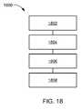
- FIG. 18is a flow chart of a method of manufacture of a package-on-package system in a further embodiment of the present invention.
- the term “horizontal” as used hereinis defined as a plane parallel to the plane or surface of the semiconductor die, regardless of its orientation.
- the term “vertical”refers to a direction perpendicular to the horizontal as just defined. Terms, such as “above”, “below”, “bottom”, “top”, “side” (as in “sidewall”), “higher”, “lower”, “upper”, “over”, and “under”, are defined with respect to the horizontal plane, as shown in the figures.
- the term “on”means that there is direct contact among elements.
- processingincludes deposition of material or photoresist, patterning, exposure, development, etching, cleaning, and/or removal of the material or photoresist as required in forming a described structure.
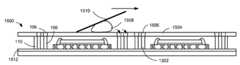
- FIG. 1therein is shown a bottom view of a package-on-package system 100 in one embodiment of the present invention.
- the package-on-package system 100includes two types of external connections 102 : substrate connections 104 and through vias 106 .
- the substrate connections 104provide an electrical path through a package substrate 108 .
- the through vias 106are located entirely within an encapsulant 110 , providing electrical connections through the package-on-package system 100 .
- the package substrate 108includes tie bars 112 extending to edges 114 of the package-on-package system 100 .
- some of the tie bars 112are configured with an offset 116 from each other.
- the package-on-package system 200includes two types of external connections 202 : substrate connections 204 and through vias 206 .
- the substrate connections 204provide an electrical path through a package substrate 208 .
- the package substrate 208has a rectangular shape that extends from an end edge 212 to an opposite edge 214 of the package-on-package system 200 .
- An encapsulant 210surrounds portions of the package substrate 208 .
- FIG. 3therein is shown a cross-sectional view of the package-on-package system 100 taken along line 3 - 3 shown in FIG. 1 .
- a semiconductor die 302is attached to the package substrate 108 using an adhesive 304 .
- Electrical interconnects 306provide connectivity between the semiconductor die 302 and the substrate connections 104 .
- the electrical interconnects 306may be implemented using bond wires as shown in FIG. 3 .
- the through vias 106extend vertically through a thickness 308 of the package-on-package system 100 providing electrical connections through the package-on-package system 100 .
- the encapsulant 110has a bottom exposed surface 310 coplanar with a bottom surface 312 of the package substrate 108 and has a top exposed surface 314 .
- the through vias 106extend from the top exposed surface 314 to the bottom exposed surface 310 of the encapsulant 110 .
- the through vias 106may be employed to provide interconnectivity between external components mounted above and below the package-on-package system 100 .
- External interconnects 316provide connectivity to the next system level.
- the package-on-package system 100can be implemented using the package substrate 108 which is minimally larger than the semiconductor die 302 , reducing the overall cost of the package-on-package system 100 .
- the package-on-package system 100is less susceptible to warping as a result of the fabrication process. Therefore it may easily be integrated as part of a larger multi-chip module.
- the package-on-package system 100may be electrically tested and classified as good known package (GKP) prior to integration into a larger module, increasing the overall reliability of a multi-chip module.
- GKPgood known package
- the package-on-package system 100 of the present inventionfurnishes important and heretofore unknown and unavailable solutions, capabilities, and functional aspects for implementing a low-cost modular package that can be stacked into a multi-level package.
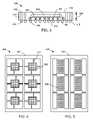
- FIG. 4therein is shown a top view of a package substrate assembly 400 incorporating the package substrate 108 of FIG. 3 .
- the package substrate assembly 400incorporates multiple repetitions of the package substrate 108 held together by a frame 402 using the tie bars 112 .
- the package substrate assembly 400is used in the fabrication of the package-on-package system 100 .
- FIG. 5therein is shown a top view of a package substrate assembly 500 incorporating the package substrate 208 in an alternate embodiment of the present invention.
- the package substrate assembly 500incorporates multiple repetitions of the package substrate 208 held together by a frame 502 .
- the package substrate assembly 500is used in the fabrication of the package-on-package system 200 .
- the package-on-package system 600includes two types of external connections 602 : substrate connections 604 and through vias 606 .
- the substrate connections 604provide an electrical path between external elements (not shown) and a semiconductor die (not shown).
- the through vias 606extend vertically through a thickness (not shown) of an encapsulant 608 , providing electrical connections between the top and bottom surface of the package-on-package system 600 .
- FIG. 7therein is shown a cross-sectional view of the package-on-package system 600 taken along line 7 - 7 shown in FIG. 6 .
- a semiconductor die 702is attached to the substrate connections 604 using an adhesive 704 .
- Electrical interconnects 706provide connectivity between the semiconductor die 702 and the substrate connections 604 .
- the electrical interconnects 706may be implemented using bond wires as shown in FIG. 7 .
- the encapsulant 608surrounds at least portions of the semiconductor die 702 , the substrate connections 604 , the electrical interconnects 706 , and the through vias 606 .
- the encapsulant 608has a bottom exposed surface 710 coplanar with a bottom surface 712 of the substrate connections 604 and has a top exposed surface 714 .
- the through vias 606extend from the top exposed surface 714 to the bottom exposed surface 710 of the encapsulant 608 .
- the through vias 606may be employed to provide interconnectivity between external components mounted above and below the package-on-package system 600 .
- External interconnects 716provide connectivity to the next system level.
- the package-on-package system 600can be implemented using the substrate connections 604 with a layout footprint minimally larger than the semiconductor die 702 , reducing the overall cost of the package-on-package system 600 . Additionally the package-on-package system 600 is less susceptible to warping as a result of the fabrication process.
- the package-on-package system 600 of the present inventionfurnishes important and heretofore unknown and unavailable solutions, capabilities, and functional aspects for implementing a low-cost modular package that can be stacked into a multi-level package.
- FIG. 8therein is shown a top view of a package substrate assembly 800 incorporating the substrate connections 604 shown in FIG. 6 .
- the package substrate assembly 800incorporates multiple repetitions of the layout for the substrate connections 604 used in each package-on-package system 600 .
- the substrate connections 604are supported by a package carrier 802 .
- the package carrier 802is a sacrificial plate such as a copper plate.
- each package substrate 900includes the package carrier 802 and the substrate connections 604 .
- the package carrier 802is a copper plate
- the substrate connections 604are plated metal traces.
- FIG. 10therein is shown a bottom view of a package-on-package system 1000 in an alternate embodiment of the present invention.
- the package-on-package system 1000includes two types of external connections 1002 accessible through its bottom surface: substrate connections 1004 and through vias 1006 .
- the substrate connections 1004provide an electrical path between external elements and a semiconductor die (not shown).
- the through vias 1006extend entirely through the encapsulant 1008 , providing electrical connections between the top and bottom surface of the package-on-package system 1000 .
- the embodiment of the invention shown in FIG. 10includes dummy patterns 1010 made using the same materials as the substrate connections 1004 .
- the dummy patterns 1010are features that are used during the fabrication process to facilitate the planarization process for the substrate connections 1004 and to reduce warping of the package-on-package system 1000 .
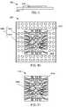
- FIG. 11therein is shown a top view of a package substrate 1100 incorporating the substrate connections 1004 and the dummy patterns 1010 used in the package-on-package system 1000 shown in FIG. 10 .
- the package carrier in the package substrate 1100is not shown for clarity.
- FIG. 12therein is shown a cross section of a mold 1200 used in the initial stages of the fabrication of the package-on-package system 100 .
- the semiconductor die 302is already attached to the package substrate 108 and connected to it using the electrical interconnects 306 .
- the package substrate 108rests on top of a bottom mold plate 1202 .
- a top mold plate 1204covers the package substrate 108 , the semiconductor die 302 , and the electrical interconnects 306 .
- the openings for the through vias 106are defined by pins 1206 extending through a molding cavity 1208 defined by the top mold plate 1204 and the bottom mold plate 1202 .
- the encapsulant(not shown) is injected through an injection port 1210 into the cavity 1208 .
- FIG. 13therein is shown a cross-section of the package-on-package system 100 of FIG. 3 following molding of the encapsulant 110 .
- the pins 1206 shown in FIG. 12define through openings 1302 extending through the encapsulant 110 .
- the through openings 1302are molds for the through vias 106 (not shown).
- the encapsulant 110has the bottom exposed surface 310 coplanar with the bottom surface 312 of the package substrate 108 and has the top exposed surface 314 .
- the through openings 1302extend from the top exposed surface 314 to the bottom exposed surface 310 of the encapsulant 110 .
- FIG. 14therein is shown a cross-section of the package-on-package system 600 of FIG. 7 following molding of the encapsulant 608 .
- the pins 1206 shown in FIG. 12define through openings 1402 extending through the encapsulant 608 .
- the through openings 1402are molds for the through vias 606 (not shown).
- the package carrier 802 of FIG. 8is dissolved following the formation of the encapsulant 608 .
- the encapsulant 608has the bottom exposed surface 710 coplanar with the bottom surface 712 of the substrate connections 604 and has a top exposed surface 714 .
- the through openings 1402extend from the top exposed surface 714 to the bottom exposed surface 710 of the encapsulant 608 .
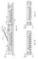
- FIG. 15therein is shown a mechanical device 1500 used to form the through vias 106 in one embodiment of the invention.
- the structure of FIG. 13is placed between a support plate 1502 and a stencil plate 1504 of the mechanical device 1500 .
- the through openings 1302previously defined by the molding of the encapsulant 110 , are aligned to openings 1506 in the stencil plate 1504 .
- the through vias 106are formed by applying solder 1508 into the through openings 1302 using a wedge 1510 . Vertical pressure on the wedge 1510 ensures filling of the through openings 1302 . A non-stick material 1512 on the support plate 1502 prevents sticking of the through vias 106 .
- FIG. 16therein is shown the package-on-package system 100 of FIG. 3 at the end of the fabrication process following the formation of the through vias 106 and the external interconnects 316 .
- FIG. 17therein is shown the package-on-package system 600 of FIG. 6 at the end of the fabrication process following the formation of the through vias 606 and the external interconnects 716 .
- the method 1800includes: providing a package substrate in a block 1802 ; attaching a semiconductor die to the package substrate in a block 1804 ; forming an encapsulant around the semiconductor die to have a bottom exposed surface coplanar with a bottom surface of the package substrate and to have a top exposed surface with through openings extending therefrom through the bottom exposed surface in a block 1806 ; and, creating through vias by applying solder into the through openings in a block 1808 .
- the resulting method, process, apparatus, device, product, and/or systemis straightforward, cost-effective, uncomplicated, highly versatile, accurate, sensitive, and effective, and can be implemented by adapting known components for ready, efficient, and economical manufacturing, application, and utilization.
- Another important aspect of the present inventionis that it valuably supports and services the historical trend of reducing costs, simplifying systems, and increasing performance.
Landscapes
- Engineering & Computer Science (AREA)
- Microelectronics & Electronic Packaging (AREA)
- Power Engineering (AREA)
- Computer Hardware Design (AREA)
- Physics & Mathematics (AREA)
- Condensed Matter Physics & Semiconductors (AREA)
- General Physics & Mathematics (AREA)
- Manufacturing & Machinery (AREA)
- Structures Or Materials For Encapsulating Or Coating Semiconductor Devices Or Solid State Devices (AREA)
- Encapsulation Of And Coatings For Semiconductor Or Solid State Devices (AREA)
Abstract
Description
- The present invention relates generally to semiconductor package system, and more particularly to a stackable package-on-package system for multi-chip modules.
- As new generations of electrical consumer products are developed there is a growing need to improve the functionality, performance, reliability, and manufacturing robustness of semiconductor packages. Additionally, new handheld consumer electronic devices such as cell phones and new laptop computers are increasingly designed to present a low-profile. This design trend imposes severe limitations on the thickness of individual electronic components.
- System requirements for consumer electronics have motivated the implementation of integrated circuit packages incorporating several semiconductor dies or “chips”. Such multi-chip packages may be realized by connecting multiple semiconductor dies on a single package substrate.
- Alternatively, the Package-in-Package (PiP) approach for packaging multi-chip modules involves first mounting a semiconductor die on a package substrate with interconnects, forming an Internal Stacking Module (ISM). This package module can be tested individually prior to assembly into a multi-chip package. Thus the PiP approach provides a means of pre-testing package sub-assemblies (i.e., internal stacking modules), enabling the assembly of complex multi-chip packages using “known good packages.” This modular approach for assembling multi-chip packages reduces overall yield loss.
- Yet another implementation of a multi-chip package is termed “Package-on-Package” (PoP). In this approach, one monolithic package is stacked on top of another package using standard interconnects for routing signals between the two packages.
- One drawback of existing PiP or PoP packages is that they do not provide sufficient versatility and reliability for integration into larger multi-chip packages. Thus, a need still remains for internal stacking module and/or package-on-package systems with increased interconnection capabilities and reduced overall thickness while improving its reliability.
- More specifically, there is a need to reduce the cost of PiP and PoP systems and to reduce warping of the modules during fabrication to facilitate integration into larger multi-chip package modules. In view of yield loss due to package warping it is increasingly critical that answers be found to these problems.
- In view of the ever-increasing commercial competitive pressures, along with growing consumer expectations and the diminishing opportunities for meaningful product differentiation in the marketplace, it is critical that answers be found for these problems. Additionally, the need to reduce costs, improve efficiencies and performance, and meet competitive pressures adds an even greater urgency to the critical necessity for finding answers to these problems.
- Solutions to these problems have been long sought but prior developments have not taught or suggested any solutions and, thus, solutions to these problems have long eluded those skilled in the art.
- The present invention provides a method of manufacture of a package-on-package system including: providing a package substrate; attaching a semiconductor die to the package substrate; forming an encapsulant around the semiconductor die to have a bottom exposed surface coplanar with a bottom surface of the package substrate and to have a top exposed surface with through openings extending therefrom through the bottom exposed surface; and creating through vias by applying solder into the through openings.
- Furthermore, the present invention provides a package-on-package system including: a package substrate; a semiconductor die attached to the package substrate; an encapsulant surrounding at least portions of the package substrate and the semiconductor die, the encapsulant having a bottom exposed surface coplanar with the bottom surface of the package substrate and a top exposed surface; and through vias extending from the top exposed surface to a bottom exposed surface of the encapsulant.
- Certain embodiments of the invention have other steps or elements in addition to or in place of those mentioned above. The steps or element will become apparent to those skilled in the art from a reading of the following detailed description when taken with reference to the accompanying drawings.
FIG. 1 is a bottom view of a package-on-package system in one embodiment of the present invention.FIG. 2 is a bottom view of the package-on-package system in an alternate embodiment of the present invention.FIG. 3 is a cross-sectional view of the package-on-package system taken along line3-3 shown inFIG. 1 .FIG. 4 is a top view of a package substrate assembly incorporating the package substrate ofFIG. 3 .FIG. 5 is a top view of a package substrate assembly incorporating a package substrate in an alternate embodiment of the present invention.FIG. 6 is a bottom view of a package-on-package system in an alternate embodiment of the present invention.FIG. 7 is a cross-sectional view of the package-on-package system taken along line7-7 shown inFIG. 6 .FIG. 8 is a top view of a package substrate assembly incorporating the substrate connections shown inFIG. 6 .FIG. 9 is a cross-section of a package substrate in thepackage substrate assembly 800 shown inFIG. 8 .FIG. 10 is a bottom view of a package-on-package system in an alternate embodiment of the present invention.FIG. 11 is a top view of a package substrate incorporating the substrate connections and the dummy patterns used in the package-on-package system shown inFIG. 10 .FIG. 12 is a cross section of a mold used in the initial stages of the fabrication of the package-on-package system.FIG. 13 is a cross-section of the package-on-package system ofFIG. 3 following molding of the encapsulant;FIG. 14 is a cross-section of the package-on-package system ofFIG. 7 following molding of the encapsulant.FIG. 15 is a mechanical device used to form the through vias in one embodiment of the invention.FIG. 16 is the package-on-package system ofFIG. 3 at the end of the fabrication process following the formation of the through vias and the external interconnects.FIG. 17 is the package-on-package system ofFIG. 6 at the end of the fabrication process following the formation of the through vias and the external interconnects.FIG. 18 is a flow chart of a method of manufacture of a package-on-package system in a further embodiment of the present invention.- The following embodiments are described in sufficient detail to enable those skilled in the art to make and use the invention. It is to be understood that other embodiments would be evident based on the present disclosure, and that system, process, or mechanical changes may be made without departing from the scope of the present invention.
- In the following description, numerous specific details are given to provide a thorough understanding of the invention. However, it will be apparent that the invention may be practiced without these specific details. In order to avoid obscuring the present invention, some well-known circuits, system configurations, and process steps are not disclosed in detail.
- The drawings showing embodiments of the system are semi-diagrammatic and not to scale and, particularly, some of the dimensions are for the clarity of presentation and are shown exaggerated in the drawing FIGs. Similarly, although the views in the drawings for ease of description generally show similar orientations, this depiction in the FIGs. is arbitrary for the most part. Generally, the invention can be operated in any orientation.
- The same numbers are used in all the drawing FIGs. to relate to the same elements. The embodiments have been numbered first embodiment, second embodiment, etc. as a matter of descriptive convenience and are not intended to have any other significance or provide limitations for the present invention.
- For expository purposes, the term “horizontal” as used herein is defined as a plane parallel to the plane or surface of the semiconductor die, regardless of its orientation. The term “vertical” refers to a direction perpendicular to the horizontal as just defined. Terms, such as “above”, “below”, “bottom”, “top”, “side” (as in “sidewall”), “higher”, “lower”, “upper”, “over”, and “under”, are defined with respect to the horizontal plane, as shown in the figures. The term “on” means that there is direct contact among elements.
- The term “processing” as used herein includes deposition of material or photoresist, patterning, exposure, development, etching, cleaning, and/or removal of the material or photoresist as required in forming a described structure.
- Referring now to
FIG. 1 , therein is shown a bottom view of a package-on-package system 100 in one embodiment of the present invention. The package-on-package system 100 includes two types of external connections102:substrate connections 104 and throughvias 106. - The
substrate connections 104 provide an electrical path through apackage substrate 108. The throughvias 106 are located entirely within an encapsulant110, providing electrical connections through the package-on-package system 100. - The
package substrate 108 includes tie bars112 extending toedges 114 of the package-on-package system 100. In one embodiment of the invention, some of the tie bars112 are configured with an offset116 from each other. - Referring now to
FIG. 2 , therein is shown a bottom view of the package-on-package system 200 in an alternate embodiment of the present invention. Similar to the package-on-package system 100, the package-on-package system 200 includes two types of external connections202:substrate connections 204 and throughvias 206. - The
substrate connections 204 provide an electrical path through apackage substrate 208. Thepackage substrate 208 has a rectangular shape that extends from anend edge 212 to anopposite edge 214 of the package-on-package system 200. Anencapsulant 210 surrounds portions of thepackage substrate 208. - Referring now to
FIG. 3 , therein is shown a cross-sectional view of the package-on-package system 100 taken along line3-3 shown inFIG. 1 . A semiconductor die302 is attached to thepackage substrate 108 using an adhesive304.Electrical interconnects 306 provide connectivity between the semiconductor die302 and thesubstrate connections 104. Theelectrical interconnects 306 may be implemented using bond wires as shown inFIG. 3 . - The through
vias 106 extend vertically through athickness 308 of the package-on-package system 100 providing electrical connections through the package-on-package system 100. Theencapsulant 110 has a bottom exposedsurface 310 coplanar with abottom surface 312 of thepackage substrate 108 and has a topexposed surface 314. The throughvias 106 extend from the top exposedsurface 314 to the bottom exposedsurface 310 of theencapsulant 110. - The through
vias 106 may be employed to provide interconnectivity between external components mounted above and below the package-on-package system 100.External interconnects 316 provide connectivity to the next system level. - It has been discovered that the package-on-
package system 100 can be implemented using thepackage substrate 108 which is minimally larger than the semiconductor die302, reducing the overall cost of the package-on-package system 100. - Additionally the package-on-
package system 100 is less susceptible to warping as a result of the fabrication process. Therefore it may easily be integrated as part of a larger multi-chip module. The package-on-package system 100 may be electrically tested and classified as good known package (GKP) prior to integration into a larger module, increasing the overall reliability of a multi-chip module. - Thus, it has been discovered that the package-on-
package system 100 of the present invention furnishes important and heretofore unknown and unavailable solutions, capabilities, and functional aspects for implementing a low-cost modular package that can be stacked into a multi-level package. - Referring now to
FIG. 4 , therein is shown a top view of apackage substrate assembly 400 incorporating thepackage substrate 108 ofFIG. 3 . Thepackage substrate assembly 400 incorporates multiple repetitions of thepackage substrate 108 held together by aframe 402 using the tie bars112. Thepackage substrate assembly 400 is used in the fabrication of the package-on-package system 100. - Referring now to
FIG. 5 , therein is shown a top view of apackage substrate assembly 500 incorporating thepackage substrate 208 in an alternate embodiment of the present invention. Thepackage substrate assembly 500 incorporates multiple repetitions of thepackage substrate 208 held together by aframe 502. Thepackage substrate assembly 500 is used in the fabrication of the package-on-package system 200. - Referring now to
FIG. 6 , therein is shown a bottom view of a package-on-package system 600 in an alternate embodiment of the present invention. The package-on-package system 600 includes two types of external connections602:substrate connections 604 and throughvias 606. Thesubstrate connections 604 provide an electrical path between external elements (not shown) and a semiconductor die (not shown). The throughvias 606 extend vertically through a thickness (not shown) of anencapsulant 608, providing electrical connections between the top and bottom surface of the package-on-package system 600. - Referring now to
FIG. 7 , therein is shown a cross-sectional view of the package-on-package system 600 taken along line7-7 shown inFIG. 6 . A semiconductor die702 is attached to thesubstrate connections 604 using an adhesive704.Electrical interconnects 706 provide connectivity between the semiconductor die702 and thesubstrate connections 604. Theelectrical interconnects 706 may be implemented using bond wires as shown inFIG. 7 . - The
encapsulant 608 surrounds at least portions of the semiconductor die702, thesubstrate connections 604, theelectrical interconnects 706, and the throughvias 606. Theencapsulant 608 has a bottom exposedsurface 710 coplanar with abottom surface 712 of thesubstrate connections 604 and has a topexposed surface 714. The throughvias 606 extend from the top exposedsurface 714 to the bottom exposedsurface 710 of theencapsulant 608. - The through
vias 606 may be employed to provide interconnectivity between external components mounted above and below the package-on-package system 600.External interconnects 716 provide connectivity to the next system level. - It has been discovered that the package-on-
package system 600 can be implemented using thesubstrate connections 604 with a layout footprint minimally larger than the semiconductor die702, reducing the overall cost of the package-on-package system 600. Additionally the package-on-package system 600 is less susceptible to warping as a result of the fabrication process. - Thus, it has been discovered that the package-on-
package system 600 of the present invention furnishes important and heretofore unknown and unavailable solutions, capabilities, and functional aspects for implementing a low-cost modular package that can be stacked into a multi-level package. - Referring now to
FIG. 8 , therein is shown a top view of apackage substrate assembly 800 incorporating thesubstrate connections 604 shown inFIG. 6 . Thepackage substrate assembly 800 incorporates multiple repetitions of the layout for thesubstrate connections 604 used in each package-on-package system 600. Thesubstrate connections 604 are supported by apackage carrier 802. In this embodiment of the invention, thepackage carrier 802 is a sacrificial plate such as a copper plate. - Referring now to
FIG. 9 , therein is shown a cross-section of apackage substrate 900 in thepackage substrate assembly 800 shown inFIG. 8 . At the initial stages of the fabrication process of the package-on-package system 600, eachpackage substrate 900 includes thepackage carrier 802 and thesubstrate connections 604. In one embodiment of the invention, thepackage carrier 802 is a copper plate, and thesubstrate connections 604 are plated metal traces. - Referring now to
FIG. 10 , therein is shown a bottom view of a package-on-package system 1000 in an alternate embodiment of the present invention. The package-on-package system 1000 includes two types ofexternal connections 1002 accessible through its bottom surface:substrate connections 1004 and throughvias 1006. Thesubstrate connections 1004 provide an electrical path between external elements and a semiconductor die (not shown). The throughvias 1006 extend entirely through theencapsulant 1008, providing electrical connections between the top and bottom surface of the package-on-package system 1000. - The embodiment of the invention shown in
FIG. 10 includesdummy patterns 1010 made using the same materials as thesubstrate connections 1004. Thedummy patterns 1010 are features that are used during the fabrication process to facilitate the planarization process for thesubstrate connections 1004 and to reduce warping of the package-on-package system 1000. - Referring now to
FIG. 11 , therein is shown a top view of apackage substrate 1100 incorporating thesubstrate connections 1004 and thedummy patterns 1010 used in the package-on-package system 1000 shown inFIG. 10 . The package carrier in thepackage substrate 1100 is not shown for clarity. - Referring now to
FIG. 12 , therein is shown a cross section of amold 1200 used in the initial stages of the fabrication of the package-on-package system 100. At this stage of the process, the semiconductor die302 is already attached to thepackage substrate 108 and connected to it using theelectrical interconnects 306. Thepackage substrate 108 rests on top of abottom mold plate 1202. Atop mold plate 1204 covers thepackage substrate 108, the semiconductor die302, and theelectrical interconnects 306. - The openings for the through
vias 106 are defined bypins 1206 extending through amolding cavity 1208 defined by thetop mold plate 1204 and thebottom mold plate 1202. The encapsulant (not shown) is injected through aninjection port 1210 into thecavity 1208. - Referring now to
FIG. 13 , therein is shown a cross-section of the package-on-package system 100 ofFIG. 3 following molding of theencapsulant 110. Thepins 1206 shown inFIG. 12 define throughopenings 1302 extending through theencapsulant 110. The throughopenings 1302 are molds for the through vias106 (not shown). - The
encapsulant 110 has the bottom exposedsurface 310 coplanar with thebottom surface 312 of thepackage substrate 108 and has the top exposedsurface 314. The throughopenings 1302 extend from the top exposedsurface 314 to the bottom exposedsurface 310 of theencapsulant 110. - Referring now to
FIG. 14 , therein is shown a cross-section of the package-on-package system 600 ofFIG. 7 following molding of theencapsulant 608. Thepins 1206 shown inFIG. 12 define throughopenings 1402 extending through theencapsulant 608. The throughopenings 1402 are molds for the through vias606 (not shown). Thepackage carrier 802 ofFIG. 8 is dissolved following the formation of theencapsulant 608. - The
encapsulant 608 has the bottom exposedsurface 710 coplanar with thebottom surface 712 of thesubstrate connections 604 and has a topexposed surface 714. The throughopenings 1402 extend from the top exposedsurface 714 to the bottom exposedsurface 710 of theencapsulant 608. - Referring now to
FIG. 15 , therein is shown amechanical device 1500 used to form the throughvias 106 in one embodiment of the invention. In this step of the fabrication process for the package-on-package system 100, the structure ofFIG. 13 is placed between a support plate1502 and astencil plate 1504 of themechanical device 1500. The throughopenings 1302, previously defined by the molding of theencapsulant 110, are aligned toopenings 1506 in thestencil plate 1504. - The through
vias 106 are formed by applyingsolder 1508 into the throughopenings 1302 using awedge 1510. Vertical pressure on thewedge 1510 ensures filling of the throughopenings 1302. Anon-stick material 1512 on the support plate1502 prevents sticking of the throughvias 106. - Referring now to
FIG. 16 , therein is shown the package-on-package system 100 ofFIG. 3 at the end of the fabrication process following the formation of the throughvias 106 and theexternal interconnects 316. - Referring now to
FIG. 17 , therein is shown the package-on-package system 600 ofFIG. 6 at the end of the fabrication process following the formation of the throughvias 606 and theexternal interconnects 716. - Referring now to
FIG. 18 , therein is shown a flow chart of amethod 1800 of manufacture of a package-on-package system 100 in a further embodiment of the present invention. Themethod 1800 includes: providing a package substrate in ablock 1802; attaching a semiconductor die to the package substrate in ablock 1804; forming an encapsulant around the semiconductor die to have a bottom exposed surface coplanar with a bottom surface of the package substrate and to have a top exposed surface with through openings extending therefrom through the bottom exposed surface in ablock 1806; and, creating through vias by applying solder into the through openings in ablock 1808. - The resulting method, process, apparatus, device, product, and/or system is straightforward, cost-effective, uncomplicated, highly versatile, accurate, sensitive, and effective, and can be implemented by adapting known components for ready, efficient, and economical manufacturing, application, and utilization.
- Another important aspect of the present invention is that it valuably supports and services the historical trend of reducing costs, simplifying systems, and increasing performance.
- These and other valuable aspects of the present invention consequently further the state of the technology to at least the next level.
- While the invention has been described in conjunction with a specific best mode, it is to be understood that many alternatives, modifications, and variations will be apparent to those skilled in the art in light of the aforegoing description. Accordingly, it is intended to embrace all such alternatives, modifications, and variations that fall within the scope of the included claims. All matters hithertofore set forth herein or shown in the accompanying drawings are to be interpreted in an illustrative and non-limiting sense.
Claims (20)
Priority Applications (5)
| Application Number | Priority Date | Filing Date | Title |
|---|---|---|---|
| US12/388,516US7986048B2 (en) | 2009-02-18 | 2009-02-18 | Package-on-package system with through vias and method of manufacture thereof |
| TW099104330ATWI475619B (en) | 2009-02-18 | 2010-02-11 | Package-on-package system with through vias and method of manufacture thereof |
| KR1020100014331AKR101715265B1 (en) | 2009-02-18 | 2010-02-17 | Package-on-package system with through vias and method of manufacture thereof |
| US13/169,387US8334601B2 (en) | 2009-02-18 | 2011-06-27 | Package-on-package system with through vias and method of manufacture thereof |
| US13/679,615US8598034B2 (en) | 2009-02-18 | 2012-11-16 | Package-on-package system with through vias and method of manufacture thereof |
Applications Claiming Priority (1)
| Application Number | Priority Date | Filing Date | Title |
|---|---|---|---|
| US12/388,516US7986048B2 (en) | 2009-02-18 | 2009-02-18 | Package-on-package system with through vias and method of manufacture thereof |
Related Child Applications (1)
| Application Number | Title | Priority Date | Filing Date |
|---|---|---|---|
| US13/169,387ContinuationUS8334601B2 (en) | 2009-02-18 | 2011-06-27 | Package-on-package system with through vias and method of manufacture thereof |
Publications (2)
| Publication Number | Publication Date |
|---|---|
| US20100207262A1true US20100207262A1 (en) | 2010-08-19 |
| US7986048B2 US7986048B2 (en) | 2011-07-26 |
Family
ID=42559183
Family Applications (3)
| Application Number | Title | Priority Date | Filing Date |
|---|---|---|---|
| US12/388,516Active2029-11-26US7986048B2 (en) | 2009-02-18 | 2009-02-18 | Package-on-package system with through vias and method of manufacture thereof |
| US13/169,387ActiveUS8334601B2 (en) | 2009-02-18 | 2011-06-27 | Package-on-package system with through vias and method of manufacture thereof |
| US13/679,615ActiveUS8598034B2 (en) | 2009-02-18 | 2012-11-16 | Package-on-package system with through vias and method of manufacture thereof |
Family Applications After (2)
| Application Number | Title | Priority Date | Filing Date |
|---|---|---|---|
| US13/169,387ActiveUS8334601B2 (en) | 2009-02-18 | 2011-06-27 | Package-on-package system with through vias and method of manufacture thereof |
| US13/679,615ActiveUS8598034B2 (en) | 2009-02-18 | 2012-11-16 | Package-on-package system with through vias and method of manufacture thereof |
Country Status (3)
| Country | Link |
|---|---|
| US (3) | US7986048B2 (en) |
| KR (1) | KR101715265B1 (en) |
| TW (1) | TWI475619B (en) |
Cited By (7)
| Publication number | Priority date | Publication date | Assignee | Title |
|---|---|---|---|---|
| US8476135B2 (en) | 2011-05-27 | 2013-07-02 | Stats Chippac Ltd. | Integrated circuit packaging system with vertical interconnects and method of manufacture thereof |
| US8816404B2 (en) | 2011-09-16 | 2014-08-26 | Stats Chippac, Ltd. | Semiconductor device and method of forming stacked semiconductor die and conductive interconnect structure through an encapsulant |
| US8970044B2 (en) | 2011-06-23 | 2015-03-03 | Stats Chippac Ltd. | Integrated circuit packaging system with vertical interconnects and method of manufacture thereof |
| US9478499B2 (en)* | 2014-07-17 | 2016-10-25 | United Microelectronics Corp. | Semiconductor package structure and method for manufacturing the same |
| US9831214B2 (en)* | 2014-06-18 | 2017-11-28 | Taiwan Semiconductor Manufacturing Company, Ltd. | Semiconductor device packages, packaging methods, and packaged semiconductor devices |
| US10177032B2 (en) | 2014-06-18 | 2019-01-08 | Taiwan Semiconductor Manufacturing Company, Ltd. | Devices, packaging devices, and methods of packaging semiconductor devices |
| US20230268290A1 (en)* | 2022-02-18 | 2023-08-24 | Western Digital Technologies, Inc. | Semiconductor Devices Having Supportive Plating Structures |
Families Citing this family (5)
| Publication number | Priority date | Publication date | Assignee | Title |
|---|---|---|---|---|
| US8525325B2 (en) | 2011-12-14 | 2013-09-03 | Stats Chippac Ltd. | Integrated circuit packaging system with leads and method of manufacture thereof |
| US8629567B2 (en) | 2011-12-15 | 2014-01-14 | Stats Chippac Ltd. | Integrated circuit packaging system with contacts and method of manufacture thereof |
| US9219029B2 (en)* | 2011-12-15 | 2015-12-22 | Stats Chippac Ltd. | Integrated circuit packaging system with terminals and method of manufacture thereof |
| US8623711B2 (en)* | 2011-12-15 | 2014-01-07 | Stats Chippac Ltd. | Integrated circuit packaging system with package-on-package and method of manufacture thereof |
| US10595411B2 (en)* | 2017-05-10 | 2020-03-17 | Power Wave Electronics Co., Ltd. | Method for manufacturing chip signal elements |
Citations (13)
| Publication number | Priority date | Publication date | Assignee | Title |
|---|---|---|---|---|
| US5111278A (en)* | 1991-03-27 | 1992-05-05 | Eichelberger Charles W | Three-dimensional multichip module systems |
| US5562971A (en)* | 1994-04-19 | 1996-10-08 | Hitachi Chemical Company, Ltd. | Multilayer printed wiring board |
| US6001671A (en)* | 1996-04-18 | 1999-12-14 | Tessera, Inc. | Methods for manufacturing a semiconductor package having a sacrificial layer |
| US6498393B2 (en)* | 1999-12-27 | 2002-12-24 | Matsushita Electric Industrial Co., Ltd. | Semiconductor device and method for the fabrication thereof |
| US6664615B1 (en)* | 2001-11-20 | 2003-12-16 | National Semiconductor Corporation | Method and apparatus for lead-frame based grid array IC packaging |
| US6984880B2 (en)* | 2001-02-14 | 2006-01-10 | Matsushita Electric Industrial Co., Ltd. | Leadframe, resin-molded semiconductor device including the leadframe, method of making the leadframe and method for manufacturing the device |
| US7208826B2 (en)* | 2000-07-05 | 2007-04-24 | Sanyo Electric Co., Ltd. | Semiconductor device and method of manufacturing the same |
| US7242081B1 (en)* | 2006-04-24 | 2007-07-10 | Advanced Semiconductor Engineering Inc. | Stacked package structure |
| US20080036050A1 (en)* | 2006-08-08 | 2008-02-14 | Lin Paul T | Package with solder-filled via holes in molding layers |
| US7436074B2 (en)* | 2005-07-14 | 2008-10-14 | Chipmos Technologies Inc. | Chip package without core and stacked chip package structure thereof |
| US20090236726A1 (en)* | 2007-12-12 | 2009-09-24 | United Test And Assembly Center Ltd. | Package-on-package semiconductor structure |
| US7662672B2 (en)* | 2006-10-13 | 2010-02-16 | Chipmos Technologies (Bermuda) Ltd. | Manufacturing process of leadframe-based BGA packages |
| US7772681B2 (en)* | 2005-06-30 | 2010-08-10 | Fairchild Semiconductor Corporation | Semiconductor die package and method for making the same |
Family Cites Families (17)
| Publication number | Priority date | Publication date | Assignee | Title |
|---|---|---|---|---|
| JP3492212B2 (en)* | 1998-08-26 | 2004-02-03 | 新光電気工業株式会社 | Semiconductor device package and method of manufacturing the same |
| JP3883784B2 (en)* | 2000-05-24 | 2007-02-21 | 三洋電機株式会社 | Plate-shaped body and method for manufacturing semiconductor device |
| US20040173894A1 (en)* | 2001-09-27 | 2004-09-09 | Amkor Technology, Inc. | Integrated circuit package including interconnection posts for multiple electrical connections |
| KR20040026530A (en)* | 2002-09-25 | 2004-03-31 | 삼성전자주식회사 | Semiconductor package and stack package using the same |
| JP4093018B2 (en)* | 2002-11-08 | 2008-05-28 | 沖電気工業株式会社 | Semiconductor device and manufacturing method thereof |
| JP2004228226A (en)* | 2003-01-21 | 2004-08-12 | Gisei Rin | Integrated circuit package carrier |
| KR100621555B1 (en)* | 2004-02-04 | 2006-09-14 | 삼성전자주식회사 | Lead frame, semiconductor chip package using same and manufacturing method thereof |
| WO2008065896A1 (en)* | 2006-11-28 | 2008-06-05 | Kyushu Institute Of Technology | Method for manufacturing semiconductor device having dual-face electrode structure and semiconductor device manufactured by the method |
| JP4415984B2 (en)* | 2006-12-06 | 2010-02-17 | ソニー株式会社 | Manufacturing method of semiconductor device |
| US7608482B1 (en)* | 2006-12-21 | 2009-10-27 | National Semiconductor Corporation | Integrated circuit package with molded insulation |
| KR101391925B1 (en)* | 2007-02-28 | 2014-05-07 | 페어차일드코리아반도체 주식회사 | Semiconductor package and semiconductor package mold for fabricating the same |
| JP5280014B2 (en)* | 2007-04-27 | 2013-09-04 | ラピスセミコンダクタ株式会社 | Semiconductor device and manufacturing method thereof |
| US7919868B2 (en)* | 2007-08-15 | 2011-04-05 | Qimonda Ag | Carrier substrate and integrated circuit |
| KR101329355B1 (en)* | 2007-08-31 | 2013-11-20 | 삼성전자주식회사 | stack-type semicondoctor package, method of forming the same and electronic system including the same |
| JP2009182202A (en)* | 2008-01-31 | 2009-08-13 | Casio Comput Co Ltd | Manufacturing method of semiconductor device |
| US7863755B2 (en)* | 2008-03-19 | 2011-01-04 | Stats Chippac Ltd. | Package-on-package system with via Z-interconnections |
| JP5043743B2 (en)* | 2008-04-18 | 2012-10-10 | ラピスセミコンダクタ株式会社 | Manufacturing method of semiconductor device |
- 2009
- 2009-02-18USUS12/388,516patent/US7986048B2/enactiveActive
- 2010
- 2010-02-11TWTW099104330Apatent/TWI475619B/enactive
- 2010-02-17KRKR1020100014331Apatent/KR101715265B1/enactiveActive
- 2011
- 2011-06-27USUS13/169,387patent/US8334601B2/enactiveActive
- 2012
- 2012-11-16USUS13/679,615patent/US8598034B2/enactiveActive
Patent Citations (13)
| Publication number | Priority date | Publication date | Assignee | Title |
|---|---|---|---|---|
| US5111278A (en)* | 1991-03-27 | 1992-05-05 | Eichelberger Charles W | Three-dimensional multichip module systems |
| US5562971A (en)* | 1994-04-19 | 1996-10-08 | Hitachi Chemical Company, Ltd. | Multilayer printed wiring board |
| US6001671A (en)* | 1996-04-18 | 1999-12-14 | Tessera, Inc. | Methods for manufacturing a semiconductor package having a sacrificial layer |
| US6498393B2 (en)* | 1999-12-27 | 2002-12-24 | Matsushita Electric Industrial Co., Ltd. | Semiconductor device and method for the fabrication thereof |
| US7208826B2 (en)* | 2000-07-05 | 2007-04-24 | Sanyo Electric Co., Ltd. | Semiconductor device and method of manufacturing the same |
| US6984880B2 (en)* | 2001-02-14 | 2006-01-10 | Matsushita Electric Industrial Co., Ltd. | Leadframe, resin-molded semiconductor device including the leadframe, method of making the leadframe and method for manufacturing the device |
| US6664615B1 (en)* | 2001-11-20 | 2003-12-16 | National Semiconductor Corporation | Method and apparatus for lead-frame based grid array IC packaging |
| US7772681B2 (en)* | 2005-06-30 | 2010-08-10 | Fairchild Semiconductor Corporation | Semiconductor die package and method for making the same |
| US7436074B2 (en)* | 2005-07-14 | 2008-10-14 | Chipmos Technologies Inc. | Chip package without core and stacked chip package structure thereof |
| US7242081B1 (en)* | 2006-04-24 | 2007-07-10 | Advanced Semiconductor Engineering Inc. | Stacked package structure |
| US20080036050A1 (en)* | 2006-08-08 | 2008-02-14 | Lin Paul T | Package with solder-filled via holes in molding layers |
| US7662672B2 (en)* | 2006-10-13 | 2010-02-16 | Chipmos Technologies (Bermuda) Ltd. | Manufacturing process of leadframe-based BGA packages |
| US20090236726A1 (en)* | 2007-12-12 | 2009-09-24 | United Test And Assembly Center Ltd. | Package-on-package semiconductor structure |
Cited By (10)
| Publication number | Priority date | Publication date | Assignee | Title |
|---|---|---|---|---|
| US8476135B2 (en) | 2011-05-27 | 2013-07-02 | Stats Chippac Ltd. | Integrated circuit packaging system with vertical interconnects and method of manufacture thereof |
| US8970044B2 (en) | 2011-06-23 | 2015-03-03 | Stats Chippac Ltd. | Integrated circuit packaging system with vertical interconnects and method of manufacture thereof |
| US8816404B2 (en) | 2011-09-16 | 2014-08-26 | Stats Chippac, Ltd. | Semiconductor device and method of forming stacked semiconductor die and conductive interconnect structure through an encapsulant |
| US9318380B2 (en) | 2011-09-16 | 2016-04-19 | Stats Chippac, Ltd. | Semiconductor device and method of forming stacked semiconductor die and conductive interconnect structure through an encapsulant |
| US9831214B2 (en)* | 2014-06-18 | 2017-11-28 | Taiwan Semiconductor Manufacturing Company, Ltd. | Semiconductor device packages, packaging methods, and packaged semiconductor devices |
| US10177032B2 (en) | 2014-06-18 | 2019-01-08 | Taiwan Semiconductor Manufacturing Company, Ltd. | Devices, packaging devices, and methods of packaging semiconductor devices |
| US9478499B2 (en)* | 2014-07-17 | 2016-10-25 | United Microelectronics Corp. | Semiconductor package structure and method for manufacturing the same |
| US9698122B2 (en) | 2014-07-17 | 2017-07-04 | United Microelectronics Corp. | Semiconductor package structure and method for manufacturing the same |
| US20230268290A1 (en)* | 2022-02-18 | 2023-08-24 | Western Digital Technologies, Inc. | Semiconductor Devices Having Supportive Plating Structures |
| US12237275B2 (en)* | 2022-02-18 | 2025-02-25 | Western Digital Technologies, Inc. | Semiconductor devices having supportive plating structures |
Also Published As
| Publication number | Publication date |
|---|---|
| US8598034B2 (en) | 2013-12-03 |
| KR101715265B1 (en) | 2017-03-10 |
| TW201037774A (en) | 2010-10-16 |
| TWI475619B (en) | 2015-03-01 |
| US20110254172A1 (en) | 2011-10-20 |
| KR20100094410A (en) | 2010-08-26 |
| US7986048B2 (en) | 2011-07-26 |
| US20130075933A1 (en) | 2013-03-28 |
| US8334601B2 (en) | 2012-12-18 |
Similar Documents
| Publication | Publication Date | Title |
|---|---|---|
| US7986048B2 (en) | Package-on-package system with through vias and method of manufacture thereof | |
| US8106500B2 (en) | Stackable integrated circuit package system | |
| US8502387B2 (en) | Integrated circuit packaging system with vertical interconnection and method of manufacture thereof | |
| US7556987B2 (en) | Method of fabricating an integrated circuit with etched ring and die paddle | |
| US7915738B2 (en) | Stackable multi-chip package system with support structure | |
| US8541872B2 (en) | Integrated circuit package system with package stacking and method of manufacture thereof | |
| US9236319B2 (en) | Stacked integrated circuit package system | |
| US8432026B2 (en) | Stackable multi-chip package system | |
| US7732901B2 (en) | Integrated circuit package system with isloated leads | |
| US8723324B2 (en) | Integrated circuit packaging system with pad connection and method of manufacture thereof | |
| US8247894B2 (en) | Integrated circuit package system with step mold recess | |
| US7956449B2 (en) | Stacked integrated circuit package system | |
| US8962393B2 (en) | Integrated circuit packaging system with heat shield and method of manufacture thereof | |
| US20080029867A1 (en) | Stackable multi-chip package system | |
| US8823160B2 (en) | Integrated circuit package system having cavity | |
| US8062934B2 (en) | Integrated circuit package system with ground bonds | |
| US9093392B2 (en) | Integrated circuit packaging system with vertical interconnection and method of manufacture thereof | |
| US8513801B2 (en) | Integrated circuit package system | |
| US20120119345A1 (en) | Integrated circuit packaging system with device mount and method of manufacture thereof |
Legal Events
| Date | Code | Title | Description |
|---|---|---|---|
| AS | Assignment | Owner name:STATS CHIPPAC LTD., SINGAPORE Free format text:ASSIGNMENT OF ASSIGNORS INTEREST;ASSIGNORS:PARK, DONGSAM;YANG, JOUNGIN;REEL/FRAME:022405/0280 Effective date:20090115 | |
| STCF | Information on status: patent grant | Free format text:PATENTED CASE | |
| FPAY | Fee payment | Year of fee payment:4 | |
| AS | Assignment | Owner name:CITICORP INTERNATIONAL LIMITED, AS COMMON SECURITY AGENT, HONG KONG Free format text:SECURITY INTEREST;ASSIGNORS:STATS CHIPPAC, INC.;STATS CHIPPAC LTD.;REEL/FRAME:036288/0748 Effective date:20150806 Owner name:CITICORP INTERNATIONAL LIMITED, AS COMMON SECURITY Free format text:SECURITY INTEREST;ASSIGNORS:STATS CHIPPAC, INC.;STATS CHIPPAC LTD.;REEL/FRAME:036288/0748 Effective date:20150806 | |
| AS | Assignment | Owner name:STATS CHIPPAC PTE. LTE., SINGAPORE Free format text:CHANGE OF NAME;ASSIGNOR:STATS CHIPPAC LTD.;REEL/FRAME:038378/0301 Effective date:20160329 | |
| MAFP | Maintenance fee payment | Free format text:PAYMENT OF MAINTENANCE FEE, 8TH YEAR, LARGE ENTITY (ORIGINAL EVENT CODE: M1552); ENTITY STATUS OF PATENT OWNER: LARGE ENTITY Year of fee payment:8 | |
| AS | Assignment | Owner name:STATS CHIPPAC PTE. LTD. FORMERLY KNOWN AS STATS CHIPPAC LTD., SINGAPORE Free format text:RELEASE BY SECURED PARTY;ASSIGNOR:CITICORP INTERNATIONAL LIMITED, AS COMMON SECURITY AGENT;REEL/FRAME:052907/0650 Effective date:20190503 Owner name:STATS CHIPPAC, INC., CALIFORNIA Free format text:RELEASE BY SECURED PARTY;ASSIGNOR:CITICORP INTERNATIONAL LIMITED, AS COMMON SECURITY AGENT;REEL/FRAME:052907/0650 Effective date:20190503 | |
| MAFP | Maintenance fee payment | Free format text:PAYMENT OF MAINTENANCE FEE, 12TH YEAR, LARGE ENTITY (ORIGINAL EVENT CODE: M1553); ENTITY STATUS OF PATENT OWNER: LARGE ENTITY Year of fee payment:12 | |
| AS | Assignment | Owner name:STATS CHIPPAC PTE. LTD., SINGAPORE Free format text:CORRECTIVE ASSIGNMENT TO CORRECT THE ASSIGNEE'S NAME PREVIOUSLY RECORDED AT REEL: 038378 FRAME: 0301. ASSIGNOR(S) HEREBY CONFIRMS THE CHANGE OF NAME;ASSIGNOR:STATS CHIPPAC LTD.;REEL/FRAME:064913/0352 Effective date:20160329 |