US20100207258A1 - Chip package and manufacturing method thereof - Google Patents
Chip package and manufacturing method thereofDownload PDFInfo
- Publication number
- US20100207258A1 US20100207258A1US12/388,761US38876109AUS2010207258A1US 20100207258 A1US20100207258 A1US 20100207258A1US 38876109 AUS38876109 AUS 38876109AUS 2010207258 A1US2010207258 A1US 2010207258A1
- Authority
- US
- United States
- Prior art keywords
- chip
- shielding layer
- substrate
- chip package
- contacts
- Prior art date
- Legal status (The legal status is an assumption and is not a legal conclusion. Google has not performed a legal analysis and makes no representation as to the accuracy of the status listed.)
- Granted
Links
- 238000004519manufacturing processMethods0.000titleclaimsdescription10
- 239000000758substrateSubstances0.000claimsabstractdescription49
- 238000000465mouldingMethods0.000claimsabstractdescription28
- 150000001875compoundsChemical class0.000claimsabstractdescription27
- 238000000034methodMethods0.000claimsdescription16
- 239000000463materialSubstances0.000claimsdescription14
- 230000008569processEffects0.000claimsdescription8
- 229910000679solderInorganic materials0.000claimsdescription6
- 238000007650screen-printingMethods0.000claimsdescription4
- 238000007747platingMethods0.000claimsdescription3
- 230000005855radiationEffects0.000abstractdescription7
- 208000032365Electromagnetic interferenceDiseases0.000abstract1
- 238000005516engineering processMethods0.000description2
- 229910052751metalInorganic materials0.000description2
- 239000002184metalSubstances0.000description2
- 238000004806packaging method and processMethods0.000description2
- 238000007639printingMethods0.000description2
- 239000004065semiconductorSubstances0.000description2
- RYGMFSIKBFXOCR-UHFFFAOYSA-NCopperChemical compound[Cu]RYGMFSIKBFXOCR-UHFFFAOYSA-N0.000description1
- 229910045601alloyInorganic materials0.000description1
- 239000000956alloySubstances0.000description1
- 230000004075alterationEffects0.000description1
- 229910052782aluminiumInorganic materials0.000description1
- XAGFODPZIPBFFR-UHFFFAOYSA-NaluminiumChemical compound[Al]XAGFODPZIPBFFR-UHFFFAOYSA-N0.000description1
- 239000003990capacitorSubstances0.000description1
- 229910052802copperInorganic materials0.000description1
- 239000010949copperSubstances0.000description1
- 238000005520cutting processMethods0.000description1
- 230000002708enhancing effectEffects0.000description1
- 238000012986modificationMethods0.000description1
- 230000004048modificationEffects0.000description1
Images


Classifications
- H—ELECTRICITY
- H01—ELECTRIC ELEMENTS
- H01L—SEMICONDUCTOR DEVICES NOT COVERED BY CLASS H10
- H01L23/00—Details of semiconductor or other solid state devices
- H01L23/02—Containers; Seals
- H01L23/04—Containers; Seals characterised by the shape of the container or parts, e.g. caps, walls
- H01L23/053—Containers; Seals characterised by the shape of the container or parts, e.g. caps, walls the container being a hollow construction and having an insulating or insulated base as a mounting for the semiconductor body
- H01L23/055—Containers; Seals characterised by the shape of the container or parts, e.g. caps, walls the container being a hollow construction and having an insulating or insulated base as a mounting for the semiconductor body the leads having a passage through the base
- H—ELECTRICITY
- H01—ELECTRIC ELEMENTS
- H01L—SEMICONDUCTOR DEVICES NOT COVERED BY CLASS H10
- H01L23/00—Details of semiconductor or other solid state devices
- H01L23/28—Encapsulations, e.g. encapsulating layers, coatings, e.g. for protection
- H01L23/31—Encapsulations, e.g. encapsulating layers, coatings, e.g. for protection characterised by the arrangement or shape
- H01L23/3107—Encapsulations, e.g. encapsulating layers, coatings, e.g. for protection characterised by the arrangement or shape the device being completely enclosed
- H01L23/3121—Encapsulations, e.g. encapsulating layers, coatings, e.g. for protection characterised by the arrangement or shape the device being completely enclosed a substrate forming part of the encapsulation
- H—ELECTRICITY
- H01—ELECTRIC ELEMENTS
- H01L—SEMICONDUCTOR DEVICES NOT COVERED BY CLASS H10
- H01L23/00—Details of semiconductor or other solid state devices
- H01L23/552—Protection against radiation, e.g. light or electromagnetic waves
- H—ELECTRICITY
- H01—ELECTRIC ELEMENTS
- H01L—SEMICONDUCTOR DEVICES NOT COVERED BY CLASS H10
- H01L2224/00—Indexing scheme for arrangements for connecting or disconnecting semiconductor or solid-state bodies and methods related thereto as covered by H01L24/00
- H01L2224/01—Means for bonding being attached to, or being formed on, the surface to be connected, e.g. chip-to-package, die-attach, "first-level" interconnects; Manufacturing methods related thereto
- H01L2224/10—Bump connectors; Manufacturing methods related thereto
- H01L2224/15—Structure, shape, material or disposition of the bump connectors after the connecting process
- H01L2224/16—Structure, shape, material or disposition of the bump connectors after the connecting process of an individual bump connector
- H01L2224/161—Disposition
- H01L2224/16151—Disposition the bump connector connecting between a semiconductor or solid-state body and an item not being a semiconductor or solid-state body, e.g. chip-to-substrate, chip-to-passive
- H01L2224/16221—Disposition the bump connector connecting between a semiconductor or solid-state body and an item not being a semiconductor or solid-state body, e.g. chip-to-substrate, chip-to-passive the body and the item being stacked
- H01L2224/16225—Disposition the bump connector connecting between a semiconductor or solid-state body and an item not being a semiconductor or solid-state body, e.g. chip-to-substrate, chip-to-passive the body and the item being stacked the item being non-metallic, e.g. insulating substrate with or without metallisation
- H—ELECTRICITY
- H01—ELECTRIC ELEMENTS
- H01L—SEMICONDUCTOR DEVICES NOT COVERED BY CLASS H10
- H01L2224/00—Indexing scheme for arrangements for connecting or disconnecting semiconductor or solid-state bodies and methods related thereto as covered by H01L24/00
- H01L2224/01—Means for bonding being attached to, or being formed on, the surface to be connected, e.g. chip-to-package, die-attach, "first-level" interconnects; Manufacturing methods related thereto
- H01L2224/42—Wire connectors; Manufacturing methods related thereto
- H01L2224/47—Structure, shape, material or disposition of the wire connectors after the connecting process
- H01L2224/48—Structure, shape, material or disposition of the wire connectors after the connecting process of an individual wire connector
- H01L2224/4805—Shape
- H01L2224/4809—Loop shape
- H01L2224/48091—Arched
- H—ELECTRICITY
- H01—ELECTRIC ELEMENTS
- H01L—SEMICONDUCTOR DEVICES NOT COVERED BY CLASS H10
- H01L2224/00—Indexing scheme for arrangements for connecting or disconnecting semiconductor or solid-state bodies and methods related thereto as covered by H01L24/00
- H01L2224/01—Means for bonding being attached to, or being formed on, the surface to be connected, e.g. chip-to-package, die-attach, "first-level" interconnects; Manufacturing methods related thereto
- H01L2224/42—Wire connectors; Manufacturing methods related thereto
- H01L2224/47—Structure, shape, material or disposition of the wire connectors after the connecting process
- H01L2224/48—Structure, shape, material or disposition of the wire connectors after the connecting process of an individual wire connector
- H01L2224/481—Disposition
- H01L2224/48151—Connecting between a semiconductor or solid-state body and an item not being a semiconductor or solid-state body, e.g. chip-to-substrate, chip-to-passive
- H01L2224/48221—Connecting between a semiconductor or solid-state body and an item not being a semiconductor or solid-state body, e.g. chip-to-substrate, chip-to-passive the body and the item being stacked
- H01L2224/48225—Connecting between a semiconductor or solid-state body and an item not being a semiconductor or solid-state body, e.g. chip-to-substrate, chip-to-passive the body and the item being stacked the item being non-metallic, e.g. insulating substrate with or without metallisation
- H01L2224/48227—Connecting between a semiconductor or solid-state body and an item not being a semiconductor or solid-state body, e.g. chip-to-substrate, chip-to-passive the body and the item being stacked the item being non-metallic, e.g. insulating substrate with or without metallisation connecting the wire to a bond pad of the item
- H—ELECTRICITY
- H01—ELECTRIC ELEMENTS
- H01L—SEMICONDUCTOR DEVICES NOT COVERED BY CLASS H10
- H01L23/00—Details of semiconductor or other solid state devices
- H01L23/48—Arrangements for conducting electric current to or from the solid state body in operation, e.g. leads, terminal arrangements ; Selection of materials therefor
- H01L23/488—Arrangements for conducting electric current to or from the solid state body in operation, e.g. leads, terminal arrangements ; Selection of materials therefor consisting of soldered or bonded constructions
- H01L23/498—Leads, i.e. metallisations or lead-frames on insulating substrates, e.g. chip carriers
- H01L23/49827—Via connections through the substrates, e.g. pins going through the substrate, coaxial cables
- H—ELECTRICITY
- H01—ELECTRIC ELEMENTS
- H01L—SEMICONDUCTOR DEVICES NOT COVERED BY CLASS H10
- H01L24/00—Arrangements for connecting or disconnecting semiconductor or solid-state bodies; Methods or apparatus related thereto
- H01L24/01—Means for bonding being attached to, or being formed on, the surface to be connected, e.g. chip-to-package, die-attach, "first-level" interconnects; Manufacturing methods related thereto
- H01L24/42—Wire connectors; Manufacturing methods related thereto
- H01L24/47—Structure, shape, material or disposition of the wire connectors after the connecting process
- H01L24/48—Structure, shape, material or disposition of the wire connectors after the connecting process of an individual wire connector
- H—ELECTRICITY
- H01—ELECTRIC ELEMENTS
- H01L—SEMICONDUCTOR DEVICES NOT COVERED BY CLASS H10
- H01L2924/00—Indexing scheme for arrangements or methods for connecting or disconnecting semiconductor or solid-state bodies as covered by H01L24/00
- H01L2924/0001—Technical content checked by a classifier
- H01L2924/00011—Not relevant to the scope of the group, the symbol of which is combined with the symbol of this group
- H—ELECTRICITY
- H01—ELECTRIC ELEMENTS
- H01L—SEMICONDUCTOR DEVICES NOT COVERED BY CLASS H10
- H01L2924/00—Indexing scheme for arrangements or methods for connecting or disconnecting semiconductor or solid-state bodies as covered by H01L24/00
- H01L2924/0001—Technical content checked by a classifier
- H01L2924/00014—Technical content checked by a classifier the subject-matter covered by the group, the symbol of which is combined with the symbol of this group, being disclosed without further technical details
- H—ELECTRICITY
- H01—ELECTRIC ELEMENTS
- H01L—SEMICONDUCTOR DEVICES NOT COVERED BY CLASS H10
- H01L2924/00—Indexing scheme for arrangements or methods for connecting or disconnecting semiconductor or solid-state bodies as covered by H01L24/00
- H01L2924/01—Chemical elements
- H01L2924/01078—Platinum [Pt]
- H—ELECTRICITY
- H01—ELECTRIC ELEMENTS
- H01L—SEMICONDUCTOR DEVICES NOT COVERED BY CLASS H10
- H01L2924/00—Indexing scheme for arrangements or methods for connecting or disconnecting semiconductor or solid-state bodies as covered by H01L24/00
- H01L2924/10—Details of semiconductor or other solid state devices to be connected
- H01L2924/11—Device type
- H01L2924/14—Integrated circuits
- H—ELECTRICITY
- H01—ELECTRIC ELEMENTS
- H01L—SEMICONDUCTOR DEVICES NOT COVERED BY CLASS H10
- H01L2924/00—Indexing scheme for arrangements or methods for connecting or disconnecting semiconductor or solid-state bodies as covered by H01L24/00
- H01L2924/19—Details of hybrid assemblies other than the semiconductor or other solid state devices to be connected
- H01L2924/1901—Structure
- H01L2924/1904—Component type
- H01L2924/19041—Component type being a capacitor
- H—ELECTRICITY
- H01—ELECTRIC ELEMENTS
- H01L—SEMICONDUCTOR DEVICES NOT COVERED BY CLASS H10
- H01L2924/00—Indexing scheme for arrangements or methods for connecting or disconnecting semiconductor or solid-state bodies as covered by H01L24/00
- H01L2924/30—Technical effects
- H01L2924/301—Electrical effects
- H01L2924/30107—Inductance
- H—ELECTRICITY
- H01—ELECTRIC ELEMENTS
- H01L—SEMICONDUCTOR DEVICES NOT COVERED BY CLASS H10
- H01L2924/00—Indexing scheme for arrangements or methods for connecting or disconnecting semiconductor or solid-state bodies as covered by H01L24/00
- H01L2924/30—Technical effects
- H01L2924/301—Electrical effects
- H01L2924/3025—Electromagnetic shielding
Definitions
- the present inventionrelates to a semiconductor device, and more particularly to a chip package.
- EMIelectromagnetic interference
- the present inventionis directed to a manufacturing method of a chip package to simplify the manufacturing process.
- the present inventionis further directed to a chip package with enhanced effectiveness of EMI shielding.
- the present inventionprovides a chip package including a laminate substrate having a plurality of contacts thereon, at least a chip disposed on the laminate substrate, a first shielding layer, a molding compound and a second shielding layer.
- the first shielding layeris disposed over the laminate substrate, exposing the contacts and the chip.
- the molding compoundencapsulates the chip, the contacts, a portion of the first shielding layer and a portion of the laminate substrate.
- the second shielding layeris disposed over the molding compound and covering the whole surface of the molding compound.
- the first or the second shielding layercan be made of solder materials, either the same or different materials.
- the chipis electrically connected to the substrate of the chip package through a plurality of wires or bumps.
- the inventionfurther provides a manufacturing method of a chip package.
- the manufacturing methodincludes the following steps. First, a substrate having a plurality of contacts and a die attaching region thereon is provided. A first shielding layer is formed over a top surface of the substrate, exposing the contacts and the die attaching region. After fixing at least a chip on the die attaching region of the substrate and bonding the chip, a molding compound is formed over the substrate to encapsulate the chip, the contacts and at least a portion of the first shielding layer. Later, a second shielding layer is formed over the molding compound.
- the first shielding layeris formed by a printing process
- the second shielding layeris formed by a printing process or a plating process.
- the first shielding layer disposed on the substratefunctions as an EMI shield of the chip package for the underneath EMI radiation.
- the chip package of the present inventionhas better EMI shielding effectiveness and improved performances.
- FIG. 1is a cross-sectional view of a chip package according to an embodiment of the present invention.
- FIGS. 2A through 2Eare schematic views showing a manufacturing method of the chip package according to the preferred embodiment of the present invention.
- FIG. 3is a cross-sectional view of a chip package according to another embodiment of the present invention.
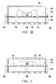
- FIG. 1is a cross-sectional view of a chip package according to a preferred embodiment of the present invention.
- the chip package 100 of the present embodimentincludes a substrate 102 , at least a chip 104 , a plurality of contacts 106 , a first shielding layer 110 , a plurality of wires 120 , a molding compound 130 and a second shielding layer 140 .
- the substrate 102can be a laminated substrate, for example, a two-layered laminated PCB substrate.
- the chip 104can be a semiconductor chip, for example, a radio-frequency (RF) chip.
- the material of the contacts 106may be copper, aluminum, or alloys thereof.
- the material of the first/second shielding layermay be a solder material, and the material of the first or second shielding layer may be different or the same.
- the contacts 106are disposed on the top surface of the substrate 102 and around the die pad 108 .
- the first shielding layer 110is disposed over the top surface of the substrate 102 , exposing the contacts 106 and the die pad 108 .
- the chip 104 disposed on the die pad 108is electrically connected to the contacts 106 of the substrate 102 through the wires 120 .
- the molding compound 130encapsulates the chip 104 , the contacts 106 , the wires 120 , a portion of the substrate 102 and a portion of the first shielding layer 110 .
- the second shielding layer 140is disposed over the molding compound 130 , covering the top surface and four side walls of the molding compound 130 .
- the second shielding layer 140covers the ground vias 105 of the substrate 102 , and the second shielding layer 140 is electrically connected to the ground via 105 and grounded. It should be noted that if the molding compound 130 completely encapsulates the chip 104 and the substrate 102 , the first shielding layer 110 covers the ground vias 105 and is grounded.
- the first shielding layer disposed on the substratefunctions as an EMI shield, particularly protecting the package from the EMI radiation from the underneath radiation sources.
- the chip package 100 of the present embodimentthere is no need for the chip package 100 of the present embodiment to include an extra metal plate and a thinner package structure can be provided.
- the first and second shielding layerscan help improve the EMI shielding of the chip package.
- the first shielding layer covering the top surface of the substratecan help shield the EMI radiation from the bottom of the chip package.
- the second shielding layer of the chip packagecovers the upper part of the chip package (exposed surfaces of the molding compound) and the first shielding layer protects the chip package from underneath underside EMI radiation, the effectiveness of the EMI shielding for the chip package is reinforced.
- the edge of the molding compoundmay be aligned with the edges of the contacts or the ground vias.
- the chip package of the present embodimentmay further include bumps on the back surface of the substrate for further connection.
- the chip packagemay be a top package in stacked package structures or package in package structures or a part of a system-in-package (SiP) structure.
- the chip package of the present inventionmay further include passive components, including resistors, capacitors, and inductors.
- FIGS. 2A through 2Eare schematic views showing a manufacturing method of the chip package according to the embodiment of the present invention.
- FIGS. 2A to 2Bare shown in top views and
- FIGS. 2C-2Eare shown in exemplary cross-sectional views.
- a substrate 102 having at least a die pad 108 and a plurality of contacts 106is provided.
- the contacts 106are arranged around the die pad 108 .
- a first shielding layer 110is formed over the top surface 102 a of the substrate 102 .
- the material of the first shielding layer 110is a solder material, for example.
- the first shielding layer 110is formed by screen printing method, for example.
- the underlying contacts 106are exposed by the corresponding first openings 112 of the first shielding layer 110 , while the die pad 108 is exposed by the second opening 114 of the first shielding layer 110 .
- the sizes of the openingsare larger than those of the correspondingly exposed components, so as to prevent possible shorts.
- the first shielding layer 110should be completely separated from the contacts 106 to prevent a short circuit from occurring.
- the size of the second opening 114may be almost equivalent to that of the die pad 108 .
- At least a chip 104is disposed on the die pad 108 and a plurality of wires 120 are formed for electrically connecting the chip 104 and the contacts 106 of the substrate 102 .
- a molding processis carried out to form a molding compound 130 on the substrate 102 to encapsulate, the chip 106 , the contacts 106 and at least a portion of the first shielding layer 110 .
- a second shielding layer 140is formed over the exposed surface of the molding compound 130 .
- the material of the second shielding layer 140is a solder material, for example.
- the second shielding layer 140is formed by screen printing method or a plating method, for example.
- a half cutting processmay be performed after forming the molding compound 130 and before forming the second shielding layer 140 .
- the chip package of the present inventionmay include a chip electrically connected to the substrate through flip chip bonding technology, rather than wire bonding technology described in the previous embodiment.
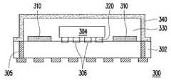
- a chip package 300further includes a chip 304 electrically connected to the contacts 306 of the substrate 302 through bumps 320 sandwiched there-between.
- the first shielding layer 310is disposed over the top surface of the substrate 302 but exposing the flip-chip area. That is, the first shielding layer 310 is completely separated from the perimeter of the flip-chip area, to prevent a short circuit between the first shielding layer and the contacts 306 /the bumps 320 from occurring.
- the molding compound 330encapsulates the chip 304 , the contacts 306 , the bumps 320 , a portion of the substrate 302 and the first shielding layer 310 .
- the second shielding layer 340is disposed over the molding compound 330 , covering the top surface and four side walls of the molding compound 330 .
- the second shielding layer 340covers the ground vias 305 of the substrate 302 , and the second shielding layer 340 is electrically connected to the ground via 305 and grounded. It should be noted that if the molding compound 330 completely encapsulates the chip 304 and the substrate 302 , the first shielding layer 310 covers the ground vias 3 05 and is grounded.
- the first and second shielding layerscan efficiently shelter the chip package of the present invention from the outside EMI radiation, thus enhancing the EMI shielding.
- the manufacturing processes disclosed in the present inventionit is possible to adapt a thinner laminate substrate without an extra ground plane and the thickness or volume of the chip package structure can be more compact. Accordingly, such design is compatible with the packaging of high frequency devices, particularly, radio frequency devices.
Landscapes
- Engineering & Computer Science (AREA)
- Microelectronics & Electronic Packaging (AREA)
- Physics & Mathematics (AREA)
- Condensed Matter Physics & Semiconductors (AREA)
- General Physics & Mathematics (AREA)
- Computer Hardware Design (AREA)
- Power Engineering (AREA)
- Health & Medical Sciences (AREA)
- Electromagnetism (AREA)
- Toxicology (AREA)
- Shielding Devices Or Components To Electric Or Magnetic Fields (AREA)
- Structures Or Materials For Encapsulating Or Coating Semiconductor Devices Or Solid State Devices (AREA)
Abstract
Description
- 1. Field of the Invention
- The present invention relates to a semiconductor device, and more particularly to a chip package.
- 2. Description of Related Art
- For most electronic devices or packages, electromagnetic interference (EMI) is a common but undesirable disturbance that may interrupt, obstruct, degrade or limit the effective performance of the devices or the whole circuit.
- Accordingly, with the increased demand in packaging of high frequency devices, weights for better EMI shielding are raised. Conventionally, extra shielding plate or ground plate may be utilized according to the related art, which results in an excessive thickness of the device and higher manufacturing costs.
- In view of the foregoing, the present invention is directed to a manufacturing method of a chip package to simplify the manufacturing process.
- The present invention is further directed to a chip package with enhanced effectiveness of EMI shielding.
- The present invention provides a chip package including a laminate substrate having a plurality of contacts thereon, at least a chip disposed on the laminate substrate, a first shielding layer, a molding compound and a second shielding layer. The first shielding layer is disposed over the laminate substrate, exposing the contacts and the chip. The molding compound encapsulates the chip, the contacts, a portion of the first shielding layer and a portion of the laminate substrate. The second shielding layer is disposed over the molding compound and covering the whole surface of the molding compound.
- According to embodiments of the present invention, the first or the second shielding layer can be made of solder materials, either the same or different materials.
- According to embodiments of the present invention, the chip is electrically connected to the substrate of the chip package through a plurality of wires or bumps.
- The invention further provides a manufacturing method of a chip package. The manufacturing method includes the following steps. First, a substrate having a plurality of contacts and a die attaching region thereon is provided. A first shielding layer is formed over a top surface of the substrate, exposing the contacts and the die attaching region. After fixing at least a chip on the die attaching region of the substrate and bonding the chip, a molding compound is formed over the substrate to encapsulate the chip, the contacts and at least a portion of the first shielding layer. Later, a second shielding layer is formed over the molding compound.
- According to one embodiment of the present invention, the first shielding layer is formed by a printing process, while the second shielding layer is formed by a printing process or a plating process.
- Based on the above, the first shielding layer disposed on the substrate functions as an EMI shield of the chip package for the underneath EMI radiation. According to the present invention, no extra metal plate is required and a complete EMI shielding is achieved through the first and second shielding layers. Therefore, the chip package of the present invention has better EMI shielding effectiveness and improved performances.
- In order to make the aforementioned and other objects, features and advantages of the present invention comprehensible, several embodiments accompanied with figures are described in detail below.
FIG. 1 is a cross-sectional view of a chip package according to an embodiment of the present invention.FIGS. 2A through 2E are schematic views showing a manufacturing method of the chip package according to the preferred embodiment of the present invention.FIG. 3 is a cross-sectional view of a chip package according to another embodiment of the present invention.FIG. 1 is a cross-sectional view of a chip package according to a preferred embodiment of the present invention. Referring toFIG. 1 , thechip package 100 of the present embodiment includes asubstrate 102, at least achip 104, a plurality ofcontacts 106, afirst shielding layer 110, a plurality ofwires 120, amolding compound 130 and a second shielding layer140. Thesubstrate 102 can be a laminated substrate, for example, a two-layered laminated PCB substrate. Thechip 104 can be a semiconductor chip, for example, a radio-frequency (RF) chip. For example, the material of thecontacts 106 may be copper, aluminum, or alloys thereof. For example, the material of the first/second shielding layer may be a solder material, and the material of the first or second shielding layer may be different or the same. Thecontacts 106 are disposed on the top surface of thesubstrate 102 and around thedie pad 108. Thefirst shielding layer 110 is disposed over the top surface of thesubstrate 102, exposing thecontacts 106 and thedie pad 108. Thechip 104 disposed on thedie pad 108 is electrically connected to thecontacts 106 of thesubstrate 102 through thewires 120. Themolding compound 130 encapsulates thechip 104, thecontacts 106, thewires 120, a portion of thesubstrate 102 and a portion of thefirst shielding layer 110. Besides, the second shielding layer140 is disposed over themolding compound 130, covering the top surface and four side walls of themolding compound 130. In addition, the second shielding layer140 covers theground vias 105 of thesubstrate 102, and the second shielding layer140 is electrically connected to the ground via105 and grounded. It should be noted that if themolding compound 130 completely encapsulates thechip 104 and thesubstrate 102, thefirst shielding layer 110 covers theground vias 105 and is grounded.- In the
chip package 100 of the present embodiment, the first shielding layer disposed on the substrate functions as an EMI shield, particularly protecting the package from the EMI radiation from the underneath radiation sources. Thus, in comparison with the chip package provided by the related art, there is no need for thechip package 100 of the present embodiment to include an extra metal plate and a thinner package structure can be provided. - The first and second shielding layers can help improve the EMI shielding of the chip package. Especially, the first shielding layer covering the top surface of the substrate can help shield the EMI radiation from the bottom of the chip package. As the second shielding layer of the chip package covers the upper part of the chip package (exposed surfaces of the molding compound) and the first shielding layer protects the chip package from underneath underside EMI radiation, the effectiveness of the EMI shielding for the chip package is reinforced.
- In the present embodiment, the edge of the molding compound may be aligned with the edges of the contacts or the ground vias. Besides, the chip package of the present embodiment may further include bumps on the back surface of the substrate for further connection. In principle, the chip package may be a top package in stacked package structures or package in package structures or a part of a system-in-package (SiP) structure. Moreover, in addition to the active component, the chip package of the present invention may further include passive components, including resistors, capacitors, and inductors.
FIGS. 2A through 2E are schematic views showing a manufacturing method of the chip package according to the embodiment of the present invention.FIGS. 2A to 2B are shown in top views andFIGS. 2C-2E are shown in exemplary cross-sectional views.- Referring to
FIG. 2A , asubstrate 102 having at least a diepad 108 and a plurality ofcontacts 106 is provided. Thecontacts 106 are arranged around thedie pad 108. - Referring to
FIG. 2B , afirst shielding layer 110 is formed over thetop surface 102a of thesubstrate 102. The material of thefirst shielding layer 110 is a solder material, for example. Thefirst shielding layer 110 is formed by screen printing method, for example. Theunderlying contacts 106 are exposed by the correspondingfirst openings 112 of thefirst shielding layer 110, while thedie pad 108 is exposed by thesecond opening 114 of thefirst shielding layer 110. In general, the sizes of the openings are larger than those of the correspondingly exposed components, so as to prevent possible shorts. In other words, thefirst shielding layer 110 should be completely separated from thecontacts 106 to prevent a short circuit from occurring. However, under certain circumstances, the size of thesecond opening 114 may be almost equivalent to that of thedie pad 108. - Referring to
FIG. 2C , at least achip 104 is disposed on thedie pad 108 and a plurality ofwires 120 are formed for electrically connecting thechip 104 and thecontacts 106 of thesubstrate 102. - Referring to
FIG. 2D , a molding process is carried out to form amolding compound 130 on thesubstrate 102 to encapsulate, thechip 106, thecontacts 106 and at least a portion of thefirst shielding layer 110. - Referring to
FIG. 2E , a second shielding layer140 is formed over the exposed surface of themolding compound 130. The material of the second shielding layer140 is a solder material, for example. The second shielding layer140 is formed by screen printing method or a plating method, for example. Optionally a half cutting process may be performed after forming themolding compound 130 and before forming the second shielding layer140. - Finally, a singulation process is performed to obtain the
chip package 100. - Alternatively, the chip package of the present invention may include a chip electrically connected to the substrate through flip chip bonding technology, rather than wire bonding technology described in the previous embodiment. As shown in
FIG. 3 , the major differences lie in that achip package 300 further includes achip 304 electrically connected to thecontacts 306 of thesubstrate 302 throughbumps 320 sandwiched there-between. Thefirst shielding layer 310 is disposed over the top surface of thesubstrate 302 but exposing the flip-chip area. That is, thefirst shielding layer 310 is completely separated from the perimeter of the flip-chip area, to prevent a short circuit between the first shielding layer and thecontacts 306/thebumps 320 from occurring. - The molding compound330 encapsulates the
chip 304, thecontacts 306, thebumps 320, a portion of thesubstrate 302 and thefirst shielding layer 310. Besides, the second shielding layer340 is disposed over the molding compound330, covering the top surface and four side walls of the molding compound330. In addition, the second shielding layer340 covers the ground vias305 of thesubstrate 302, and the second shielding layer340 is electrically connected to the ground via305 and grounded. It should be noted that if the molding compound330 completely encapsulates thechip 304 and thesubstrate 302, thefirst shielding layer 310 covers the ground vias305 and is grounded. - In summary, the first and second shielding layers can efficiently shelter the chip package of the present invention from the outside EMI radiation, thus enhancing the EMI shielding. Following the manufacturing processes disclosed in the present invention, it is possible to adapt a thinner laminate substrate without an extra ground plane and the thickness or volume of the chip package structure can be more compact. Accordingly, such design is compatible with the packaging of high frequency devices, particularly, radio frequency devices.
- Although the present invention has been disclosed above by the embodiments, they are not intended to limit the present invention. Anybody skilled in the art can make some modifications and alteration without departing from the spirit and scope of the present invention. Therefore, the protecting range of the present invention falls in the appended claims.
Claims (16)
Priority Applications (3)
| Application Number | Priority Date | Filing Date | Title |
|---|---|---|---|
| US12/388,761US8110902B2 (en) | 2009-02-19 | 2009-02-19 | Chip package and manufacturing method thereof |
| TW98127894ATWI471985B (en) | 2009-02-19 | 2009-08-19 | Chip package and manufacturing method thereof |
| CN2009101713429ACN101814484B (en) | 2009-02-19 | 2009-08-27 | Chip package and manufacturing method thereof |
Applications Claiming Priority (1)
| Application Number | Priority Date | Filing Date | Title |
|---|---|---|---|
| US12/388,761US8110902B2 (en) | 2009-02-19 | 2009-02-19 | Chip package and manufacturing method thereof |
Publications (2)
| Publication Number | Publication Date |
|---|---|
| US20100207258A1true US20100207258A1 (en) | 2010-08-19 |
| US8110902B2 US8110902B2 (en) | 2012-02-07 |
Family
ID=42559180
Family Applications (1)
| Application Number | Title | Priority Date | Filing Date |
|---|---|---|---|
| US12/388,761Expired - Fee RelatedUS8110902B2 (en) | 2009-02-19 | 2009-02-19 | Chip package and manufacturing method thereof |
Country Status (3)
| Country | Link |
|---|---|
| US (1) | US8110902B2 (en) |
| CN (1) | CN101814484B (en) |
| TW (1) | TWI471985B (en) |
Cited By (61)
| Publication number | Priority date | Publication date | Assignee | Title |
|---|---|---|---|---|
| US20100109132A1 (en)* | 2008-10-31 | 2010-05-06 | Advanced Semiconductor Engineering, Inc. | Chip package and manufacturing method thereof |
| US20100207257A1 (en)* | 2009-02-17 | 2010-08-19 | Advanced Semiconductor Engineering, Inc. | Semiconductor package and manufacturing method thereof |
| US20100207259A1 (en)* | 2008-02-05 | 2010-08-19 | Advanced Semiconductor Engineering, Inc. | Semiconductor device packages with electromagnetic interference shielding |
| US20110090659A1 (en)* | 2009-10-16 | 2011-04-21 | Kuo-Hsien Liao | Package Having An Inner Shield And Method For Making The Same |
| US7989928B2 (en) | 2008-02-05 | 2011-08-02 | Advanced Semiconductor Engineering Inc. | Semiconductor device packages with electromagnetic interference shielding |
| US8022511B2 (en) | 2008-02-05 | 2011-09-20 | Advanced Semiconductor Engineering, Inc. | Semiconductor device packages with electromagnetic interference shielding |
| US8030750B2 (en) | 2009-11-19 | 2011-10-04 | Advanced Semiconductor Engineering, Inc. | Semiconductor device packages with electromagnetic interference shielding |
| US20120104571A1 (en)* | 2010-10-27 | 2012-05-03 | Samsung Electro-Mechanics Co., Ltd. | Semiconductor package and manufacturing method thereof |
| US20120133032A1 (en)* | 2010-11-26 | 2012-05-31 | Siliconware Precision Industries Co., Ltd. | Package having esd and emi preventing functions and fabrication method thereof |
| US8212340B2 (en) | 2009-07-13 | 2012-07-03 | Advanced Semiconductor Engineering, Inc. | Chip package and manufacturing method thereof |
| US20120170162A1 (en)* | 2011-01-05 | 2012-07-05 | Siliconware Precision Industries Co., Ltd. | Semiconductor package and fabrication method thereof |
| US20120211876A1 (en)* | 2011-02-23 | 2012-08-23 | Azurewave Technologies, Inc. | Module ic package structure |
| JP2012164913A (en)* | 2011-02-09 | 2012-08-30 | Murata Mfg Co Ltd | Method of manufacturing high frequency module, and high frequency module |
| US8350367B2 (en) | 2008-02-05 | 2013-01-08 | Advanced Semiconductor Engineering, Inc. | Semiconductor device packages with electromagnetic interference shielding |
| US8368185B2 (en) | 2009-11-19 | 2013-02-05 | Advanced Semiconductor Engineering, Inc. | Semiconductor device packages with electromagnetic interference shielding |
| US8378466B2 (en) | 2009-11-19 | 2013-02-19 | Advanced Semiconductor Engineering, Inc. | Wafer-level semiconductor device packages with electromagnetic interference shielding |
| US8410584B2 (en) | 2008-08-08 | 2013-04-02 | Advanced Semiconductor Engineering, Inc. | Semiconductor device packages with electromagnetic interference shielding |
| US20130223041A1 (en)* | 2012-02-23 | 2013-08-29 | Apple Inc. | Low profile, space efficient circuit shields |
| US8541883B2 (en) | 2011-11-29 | 2013-09-24 | Advanced Semiconductor Engineering, Inc. | Semiconductor device having shielded conductive vias |
| US20130320513A1 (en)* | 2012-06-04 | 2013-12-05 | Siliconware Precision Industries Co., Ltd. | Semiconductor package and fabrication method thereof |
| US8653634B2 (en) | 2012-06-11 | 2014-02-18 | Advanced Semiconductor Engineering, Inc. | EMI-shielded semiconductor devices and methods of making |
| US8704341B2 (en) | 2012-05-15 | 2014-04-22 | Advanced Semiconductor Engineering, Inc. | Semiconductor packages with thermal dissipation structures and EMI shielding |
| US8786060B2 (en) | 2012-05-04 | 2014-07-22 | Advanced Semiconductor Engineering, Inc. | Semiconductor package integrated with conformal shield and antenna |
| US20140308907A1 (en)* | 2013-04-16 | 2014-10-16 | Skyworks Solutions, Inc. | Apparatus and methods related to ground paths implemented with surface mount devices |
| US8884424B2 (en) | 2010-01-13 | 2014-11-11 | Advanced Semiconductor Engineering, Inc. | Semiconductor package with single sided substrate design and manufacturing methods thereof |
| US8937376B2 (en) | 2012-04-16 | 2015-01-20 | Advanced Semiconductor Engineering, Inc. | Semiconductor packages with heat dissipation structures and related methods |
| US20150076701A1 (en)* | 2013-09-13 | 2015-03-19 | Kabushiki Kaisha Toshiba | Semiconductor device |
| US9007273B2 (en) | 2010-09-09 | 2015-04-14 | Advances Semiconductor Engineering, Inc. | Semiconductor package integrated with conformal shield and antenna |
| US20150124421A1 (en)* | 2005-08-08 | 2015-05-07 | Rf Micro Devices, Inc. | Electronic modules having grounded electromagnetic shields |
| US20150171022A1 (en)* | 2013-12-16 | 2015-06-18 | Utac Thai Limited | Conductive shield for semiconductor package |
| US9070793B2 (en) | 2010-08-02 | 2015-06-30 | Advanced Semiconductor Engineering, Inc. | Semiconductor device packages having electromagnetic interference shielding and related methods |
| US9153542B2 (en) | 2012-08-01 | 2015-10-06 | Advanced Semiconductor Engineering, Inc. | Semiconductor package having an antenna and manufacturing method thereof |
| US9236356B2 (en) | 2013-07-31 | 2016-01-12 | Advanced Semiconductor Engineering, Inc. | Semiconductor package with grounding and shielding layers |
| US20160035678A1 (en)* | 2014-07-30 | 2016-02-04 | Samsung Electro-Mechanics Co., Ltd. | Semiconductor package and method of manufacturing the same |
| US9349611B2 (en) | 2010-03-22 | 2016-05-24 | Advanced Semiconductor Engineering, Inc. | Stackable semiconductor package and manufacturing method thereof |
| US9406658B2 (en) | 2010-12-17 | 2016-08-02 | Advanced Semiconductor Engineering, Inc. | Embedded component device and manufacturing methods thereof |
| US9420704B2 (en) | 2011-02-25 | 2016-08-16 | Qorvo Us, Inc. | Connection using conductive vias |
| US20160254236A1 (en)* | 2015-02-27 | 2016-09-01 | Qualcomm Incorporated | Compartment shielding in flip-chip (fc) module |
| US9490219B2 (en)* | 2014-05-16 | 2016-11-08 | Siliconware Precision Industries Co., Ltd. | Semiconductor package with shielding member and method of manufacturing the same |
| US9627230B2 (en) | 2011-02-28 | 2017-04-18 | Qorvo Us, Inc. | Methods of forming a microshield on standard QFN package |
| US9673150B2 (en) | 2014-12-16 | 2017-06-06 | Nxp Usa, Inc. | EMI/RFI shielding for semiconductor device packages |
| WO2017112252A1 (en)* | 2015-12-22 | 2017-06-29 | Intel Corporation | Semiconductor package with trenched molding-based electromagnetic interference shielding |
| US20170263470A1 (en)* | 2013-03-08 | 2017-09-14 | STATS ChipPAC Pte. Ltd. | Semiconductor Device and Method of Forming Embedded Conductive Layer for Power/Ground Planes in FO-EWLB |
| US9807890B2 (en) | 2013-05-31 | 2017-10-31 | Qorvo Us, Inc. | Electronic modules having grounded electromagnetic shields |
| CN107305883A (en)* | 2016-04-22 | 2017-10-31 | 矽品精密工业股份有限公司 | Electronic package and manufacturing method thereof |
| US9826630B2 (en) | 2014-09-04 | 2017-11-21 | Nxp Usa, Inc. | Fan-out wafer level packages having preformed embedded ground plane connections and methods for the fabrication thereof |
| US9978688B2 (en) | 2013-02-28 | 2018-05-22 | Advanced Semiconductor Engineering, Inc. | Semiconductor package having a waveguide antenna and manufacturing method thereof |
| US20180294545A1 (en)* | 2017-04-10 | 2018-10-11 | City University Of Hong Kong | Chip-and-package distributed antenna |
| US10157858B2 (en) | 2017-02-24 | 2018-12-18 | SK Hynix Inc. | Semiconductor package having an electro-magnetic interference shielding or electro-magnetic wave scattering structure |
| EP3428965A1 (en)* | 2017-07-13 | 2019-01-16 | MediaTek Inc. | Semiconductor package including emi shielding structure and method for forming the same |
| US10242953B1 (en) | 2015-05-27 | 2019-03-26 | Utac Headquarters PTE. Ltd | Semiconductor package with plated metal shielding and a method thereof |
| US10242934B1 (en) | 2014-05-07 | 2019-03-26 | Utac Headquarters Pte Ltd. | Semiconductor package with full plating on contact side surfaces and methods thereof |
| US10352969B2 (en)* | 2016-11-29 | 2019-07-16 | Allegro Microsystems, Llc | Systems and methods for integrated shielding in a current sensor |
| US10971455B2 (en)* | 2019-05-01 | 2021-04-06 | Qualcomm Incorporated | Ground shield plane for ball grid array (BGA) package |
| US11058038B2 (en) | 2018-06-28 | 2021-07-06 | Qorvo Us, Inc. | Electromagnetic shields for sub-modules |
| US11114363B2 (en) | 2018-12-20 | 2021-09-07 | Qorvo Us, Inc. | Electronic package arrangements and related methods |
| US11127689B2 (en) | 2018-06-01 | 2021-09-21 | Qorvo Us, Inc. | Segmented shielding using wirebonds |
| US11183466B2 (en)* | 2019-05-28 | 2021-11-23 | Samsung Electronics Co., Ltd. | Semiconductor package including an electromagnetic shield and method of fabricating the same |
| US20220028704A1 (en)* | 2018-12-18 | 2022-01-27 | Octavo Systems Llc | Molded packages in a molded device |
| CN114725069A (en)* | 2022-04-08 | 2022-07-08 | 宁波芯健半导体有限公司 | A packaged device and a method for making the same |
| US11515282B2 (en) | 2019-05-21 | 2022-11-29 | Qorvo Us, Inc. | Electromagnetic shields with bonding wires for sub-modules |
Families Citing this family (27)
| Publication number | Priority date | Publication date | Assignee | Title |
|---|---|---|---|---|
| JPWO2009144960A1 (en)* | 2008-05-30 | 2011-10-06 | 三洋電機株式会社 | Semiconductor module, semiconductor module manufacturing method, and portable device |
| TWI497679B (en)* | 2009-11-27 | 2015-08-21 | Advanced Semiconductor Eng | Semiconductor package and manufacturing method thereof |
| TWI489610B (en)* | 2010-01-18 | 2015-06-21 | 矽品精密工業股份有限公司 | Method for making emi shielding package structure |
| US8227903B2 (en)* | 2010-09-15 | 2012-07-24 | Stats Chippac Ltd | Integrated circuit packaging system with encapsulant containment and method of manufacture thereof |
| US8654537B2 (en)* | 2010-12-01 | 2014-02-18 | Apple Inc. | Printed circuit board with integral radio-frequency shields |
| KR101711045B1 (en) | 2010-12-02 | 2017-03-02 | 삼성전자 주식회사 | Stacked Package Structure |
| US8279625B2 (en) | 2010-12-14 | 2012-10-02 | Apple Inc. | Printed circuit board radio-frequency shielding structures |
| US9179538B2 (en) | 2011-06-09 | 2015-11-03 | Apple Inc. | Electromagnetic shielding structures for selectively shielding components on a substrate |
| CN103137595A (en)* | 2011-11-25 | 2013-06-05 | 亚旭电子科技(江苏)有限公司 | System-level encapsulation module part and manufacturing method thereof |
| TWI474462B (en)* | 2011-12-16 | 2015-02-21 | 矽品精密工業股份有限公司 | Semiconductor package and method of forming same |
| US9947606B2 (en) | 2012-04-26 | 2018-04-17 | Sandisk Information Technology (Shanghai) Co., Ltd. | Semiconductor device including electromagnetic absorption and shielding |
| CN102969303A (en)* | 2012-10-26 | 2013-03-13 | 日月光半导体制造股份有限公司 | Semiconductor package structure and manufacturing method thereof |
| US9837701B2 (en) | 2013-03-04 | 2017-12-05 | Advanced Semiconductor Engineering, Inc. | Semiconductor package including antenna substrate and manufacturing method thereof |
| US9129954B2 (en) | 2013-03-07 | 2015-09-08 | Advanced Semiconductor Engineering, Inc. | Semiconductor package including antenna layer and manufacturing method thereof |
| US9172131B2 (en) | 2013-03-15 | 2015-10-27 | Advanced Semiconductor Engineering, Inc. | Semiconductor structure having aperture antenna |
| TW201513275A (en)* | 2013-09-17 | 2015-04-01 | Chipmos Technologies Inc | Chip package structure and manufacturing method thereof |
| CN103589631B (en)* | 2013-11-19 | 2015-04-22 | 苏州晶方半导体科技股份有限公司 | Biological chip packaging structure and packaging method |
| KR102354370B1 (en)* | 2015-04-29 | 2022-01-21 | 삼성전자주식회사 | Magneto-resistive chip package including a shielding structure |
| US10141268B2 (en) | 2015-10-30 | 2018-11-27 | Avago Technologies International Sales Pte. Limited | Circuit package with internal and external shielding |
| US9685413B1 (en)* | 2016-04-01 | 2017-06-20 | Intel Corporation | Semiconductor package having an EMI shielding layer |
| CN106340506A (en)* | 2016-10-20 | 2017-01-18 | 江苏长电科技股份有限公司 | Semiconductor packaging structure and manufacturing method thereof |
| CN106816432A (en)* | 2016-12-22 | 2017-06-09 | 创智能科技股份有限公司 | Packaging structure with antistatic structure |
| CN107481997A (en)* | 2017-09-05 | 2017-12-15 | 中国电子科技集团公司第二十九研究所 | A double-layer stacked hermetic packaging structure and method |
| US11038267B2 (en)* | 2018-07-31 | 2021-06-15 | Skyworks Solutions, Inc. | Apparatus and methods for electromagnetic shielding using an outer cobalt layer |
| CN109755185A (en)* | 2019-01-03 | 2019-05-14 | 长江存储科技有限责任公司 | Package structure and packaging method of semiconductor device |
| CN110010507A (en)* | 2019-04-04 | 2019-07-12 | 中电海康无锡科技有限公司 | SIP module subregion is electromagnetically shielded packaging method |
| CN111987003B (en)* | 2020-08-26 | 2022-04-01 | 中国电子科技集团公司第十三研究所 | Method for realizing electromagnetic shielding function of GaAs chip and GaAs chip |
Citations (91)
| Publication number | Priority date | Publication date | Assignee | Title |
|---|---|---|---|---|
| US3390226A (en)* | 1964-10-19 | 1968-06-25 | Siemens Ag | Encapsulated semiconductor element |
| US4569786A (en)* | 1983-04-12 | 1986-02-11 | Ube Industries, Ltd. | Electrically conductive thermoplastic resin composition containing metal and carbon fibers |
| US4717948A (en)* | 1983-03-18 | 1988-01-05 | Mitsubishi Denki Kabushiki Kaisha | Semiconductor device |
| US4821007A (en)* | 1987-02-06 | 1989-04-11 | Tektronix, Inc. | Strip line circuit component and method of manufacture |
| US5104745A (en)* | 1989-07-06 | 1992-04-14 | Gec Alsthom Sa | Multifilament superconductor strand having an anti-diffusion barrier layer |
| US5166772A (en)* | 1991-02-22 | 1992-11-24 | Motorola, Inc. | Transfer molded semiconductor device package with integral shield |
| US5172077A (en)* | 1991-04-27 | 1992-12-15 | Murata Manufacturing Co., Ltd. | Oscillator and method of manufacturing the same |
| US5355016A (en)* | 1993-05-03 | 1994-10-11 | Motorola, Inc. | Shielded EPROM package |
| US5353498A (en)* | 1993-02-08 | 1994-10-11 | General Electric Company | Method for fabricating an integrated circuit module |
| US5557142A (en)* | 1991-02-04 | 1996-09-17 | Motorola, Inc. | Shielded semiconductor device package |
| US5600181A (en)* | 1995-05-24 | 1997-02-04 | Lockheed Martin Corporation | Hermetically sealed high density multi-chip package |
| US5639989A (en)* | 1994-04-19 | 1997-06-17 | Motorola Inc. | Shielded electronic component assembly and method for making the same |
| US5677511A (en)* | 1995-03-20 | 1997-10-14 | National Semiconductor Corporation | Overmolded PC board with ESD protection and EMI suppression |
| US5694300A (en)* | 1996-04-01 | 1997-12-02 | Northrop Grumman Corporation | Electromagnetically channelized microwave integrated circuit |
| US5703761A (en)* | 1995-09-07 | 1997-12-30 | Siemens Aktiengesellschaft | Shielding for flat modules |
| US5726612A (en)* | 1992-12-01 | 1998-03-10 | Murata Manufacturing Co., Ltd. | Chip-type electronic component |
| US5729437A (en)* | 1994-06-22 | 1998-03-17 | Seiko Epson Corporation | Electronic part including a thin body of molding resin |
| US5776798A (en)* | 1996-09-04 | 1998-07-07 | Motorola, Inc. | Semiconductor package and method thereof |
| US5847930A (en)* | 1995-10-13 | 1998-12-08 | Hei, Inc. | Edge terminals for electronic circuit modules |
| US5864088A (en)* | 1994-01-20 | 1999-01-26 | Tokin Corporation | Electronic device having the electromagnetic interference suppressing body |
| US5886876A (en)* | 1995-12-13 | 1999-03-23 | Oki Electric Industry Co., Ltd. | Surface-mounted semiconductor package and its manufacturing method |
| US5895229A (en)* | 1997-05-19 | 1999-04-20 | Motorola, Inc. | Microelectronic package including a polymer encapsulated die, and method for forming same |
| US5898344A (en)* | 1996-03-14 | 1999-04-27 | Tdk Corporation | High-frequency module |
| US5966052A (en)* | 1997-04-09 | 1999-10-12 | Murata Manufacturing Co., Ltd. | Voltage-controlled oscillator with input and output on opposite corners of substrate |
| US5977626A (en)* | 1998-08-12 | 1999-11-02 | Industrial Technology Research Institute | Thermally and electrically enhanced PBGA package |
| US5998867A (en)* | 1996-02-23 | 1999-12-07 | Honeywell Inc. | Radiation enhanced chip encapsulant |
| US6079099A (en)* | 1996-06-24 | 2000-06-27 | Sumitomo Metal Industries Limited | Electronic component manufacturing method |
| US6150193A (en)* | 1996-10-31 | 2000-11-21 | Amkor Technology, Inc. | RF shielded device |
| US6194250B1 (en)* | 1998-09-14 | 2001-02-27 | Motorola, Inc. | Low-profile microelectronic package |
| US6225694B1 (en)* | 1997-09-02 | 2001-05-01 | Oki Electric Industry Co, Ltd. | Semiconductor device |
| US6255143B1 (en)* | 1999-08-04 | 2001-07-03 | St. Assembly Test Services Pte Ltd. | Flip chip thermally enhanced ball grid array |
| US6261680B1 (en)* | 1999-12-07 | 2001-07-17 | Hughes Electronics Corporation | Electronic assembly with charge-dissipating transparent conformal coating |
| US6369335B1 (en)* | 1999-04-02 | 2002-04-09 | Murata Manufacturing Co., Ltd | Mother substrate, substrate element and method for manufacturing the same |
| US6376769B1 (en)* | 1999-05-18 | 2002-04-23 | Amerasia International Technology, Inc. | High-density electronic package, and method for making same |
| US20020053724A1 (en)* | 2000-09-13 | 2002-05-09 | Siliconware Precision Industries Co., Ltd. | Semiconductor package |
| US20020093108A1 (en)* | 2001-01-15 | 2002-07-18 | Grigorov Ilya L. | Flip chip packaged semiconductor device having double stud bumps and method of forming same |
| US6448632B1 (en)* | 2000-08-28 | 2002-09-10 | National Semiconductor Corporation | Metal coated markings on integrated circuit devices |
| US6455864B1 (en)* | 1994-04-01 | 2002-09-24 | Maxwell Electronic Components Group, Inc. | Methods and compositions for ionizing radiation shielding |
| US6472743B2 (en)* | 2001-02-22 | 2002-10-29 | Siliconware Precision Industries, Co., Ltd. | Semiconductor package with heat dissipating structure |
| US6472598B1 (en)* | 1998-08-28 | 2002-10-29 | Amkor Technology, Inc. | Electromagnetic interference shield device with conductive encapsulant and dam |
| US6492194B1 (en)* | 1999-10-15 | 2002-12-10 | Thomson-Csf | Method for the packaging of electronic components |
| US6521978B2 (en)* | 2000-01-24 | 2003-02-18 | Infineon Technologies Ag | Shielding device and electrical structural part having a shielding device |
| US6566596B1 (en)* | 1997-12-29 | 2003-05-20 | Intel Corporation | Magnetic and electric shielding of on-board devices |
| US6586822B1 (en)* | 2000-09-08 | 2003-07-01 | Intel Corporation | Integrated core microelectronic package |
| US6602737B2 (en)* | 2001-04-18 | 2003-08-05 | Siliconware Precision Industries Co., Ltd. | Semiconductor package with heat-dissipating structure and method of making the same |
| US6635953B2 (en)* | 2001-01-09 | 2003-10-21 | Taiwan Electronic Packaging Co., Ltd. | IC chip package |
| US6695985B2 (en)* | 2001-06-12 | 2004-02-24 | Nitto Denko Corporation | Electromagnetic wave suppressor sheet |
| US20040063242A1 (en)* | 2002-09-17 | 2004-04-01 | Chippac, Inc. | Semiconductor multi-package module having package stacked over ball grid array package and having wire bond interconnect between stacked packages |
| US6800804B2 (en)* | 2001-06-12 | 2004-10-05 | Nitto Denko Corporation | Epoxy resin composition used for encapsulating semiconductor and semiconductor device using the composition |
| US6838776B2 (en)* | 2003-04-18 | 2005-01-04 | Freescale Semiconductor, Inc. | Circuit device with at least partial packaging and method for forming |
| US6856007B2 (en)* | 2001-08-28 | 2005-02-15 | Tessera, Inc. | High-frequency chip packages |
| US6867480B2 (en)* | 2003-06-10 | 2005-03-15 | Lsi Logic Corporation | Electromagnetic interference package protection |
| US6900383B2 (en)* | 2001-03-19 | 2005-05-31 | Hewlett-Packard Development Company, L.P. | Board-level EMI shield that adheres to and conforms with printed circuit board component and board surfaces |
| US6928719B2 (en)* | 2001-12-07 | 2005-08-16 | Samsung Electro-Mechanics Co., Ltd. | Method for fabricating surface acoustic wave filter package |
| US6967403B2 (en)* | 2003-06-18 | 2005-11-22 | Advanced Semiconductor Engineering, Inc. | Package structure with a heat spreader and manufacturing method thereof |
| US6975516B2 (en)* | 2001-10-18 | 2005-12-13 | Matsushita Electric Industrial Co., Ltd. | Component built-in module and method for producing the same |
| US6992400B2 (en)* | 2004-01-30 | 2006-01-31 | Nokia Corporation | Encapsulated electronics device with improved heat dissipation |
| US7049682B1 (en)* | 2001-05-14 | 2006-05-23 | Amkor Technology, Inc. | Multi-chip semiconductor package with integral shield and antenna |
| US20060148317A1 (en)* | 2005-01-05 | 2006-07-06 | Sadakazu Akaike | Semiconductor device |
| US20060160261A1 (en)* | 2005-01-20 | 2006-07-20 | Nanosolar, Inc. | Series interconnected optoelectronic device module assembly |
| US7126218B1 (en)* | 2001-08-07 | 2006-10-24 | Amkor Technology, Inc. | Embedded heat spreader ball grid array |
| US7125744B2 (en)* | 2001-03-16 | 2006-10-24 | Matsushita Electric Industrial Co., Ltd. | High-frequency module and method for manufacturing the same |
| US20070030661A1 (en)* | 2005-08-08 | 2007-02-08 | Rf Micro Devices, Inc. | Conformal electromagnetic interference shield |
| US7180012B2 (en)* | 2002-08-29 | 2007-02-20 | Mitsushita Electric Industrial Co., Ltd. | Module part |
| US7183498B2 (en)* | 2004-10-05 | 2007-02-27 | Matsushita Electric Industrial Co., Ltd. | High-frequency module and electronic device using the module |
| US20070241437A1 (en)* | 2006-04-17 | 2007-10-18 | Elpida Memory, Inc. | Stacked semiconductor device and fabrication method for same |
| US7372151B1 (en)* | 2003-09-12 | 2008-05-13 | Asat Ltd. | Ball grid array package and process for manufacturing same |
| US20080128890A1 (en)* | 2006-11-30 | 2008-06-05 | Advanced Semiconductor Engineering, Inc. | Chip package and fabricating process thereof |
| US7446265B2 (en)* | 2005-04-15 | 2008-11-04 | Parker Hannifin Corporation | Board level shielding module |
| US7445968B2 (en)* | 2005-12-16 | 2008-11-04 | Sige Semiconductor (U.S.), Corp. | Methods for integrated circuit module packaging and integrated circuit module packages |
| US20090027863A1 (en)* | 2003-04-04 | 2009-01-29 | Marcos Karnezos | Method for making a semiconductor multipackage module including a processor and memory package assemblies |
| US7488903B2 (en)* | 2005-11-28 | 2009-02-10 | Murata Manufacturing Co., Ltd. | Method for manufacturing circuit modules and circuit module |
| US20090075428A1 (en)* | 2007-09-13 | 2009-03-19 | Freescale Semiconductor, Inc. | Electromagnetic shield formation for integrated circuit die package |
| US20090102033A1 (en)* | 2007-10-18 | 2009-04-23 | Elmos Advanced Packaging B.V. | Integrated circuit package |
| US20090152688A1 (en)* | 2007-12-13 | 2009-06-18 | Byung Tai Do | Integrated circuit package system for shielding electromagnetic interference |
| US20090230487A1 (en)* | 2005-03-16 | 2009-09-17 | Yamaha Corporation | Semiconductor device, semiconductor device manufacturing method and lid frame |
| US20090294928A1 (en)* | 2008-05-28 | 2009-12-03 | Stats Chippac, Ltd. | Semiconductor Device and Method of Forming Holes In Substrate to Interconnect Top Shield and Ground Shield |
| US20090302446A1 (en)* | 2007-12-28 | 2009-12-10 | Kuo-Yuan Lee | Semiconductor package fabricated by cutting and molding in small windows |
| US7643311B2 (en)* | 2005-04-21 | 2010-01-05 | Stmicroelectronics Sa | Electronic circuit protection device |
| US20100006330A1 (en)* | 2008-07-11 | 2010-01-14 | Advanced Semiconductor Engineering, Inc. | Structure and process of embedded chip package |
| US7741151B2 (en)* | 2008-11-06 | 2010-06-22 | Freescale Semiconductor, Inc. | Integrated circuit package formation |
| US7745910B1 (en)* | 2007-07-10 | 2010-06-29 | Amkor Technology, Inc. | Semiconductor device having RF shielding and method therefor |
| US7772046B2 (en)* | 2008-06-04 | 2010-08-10 | Stats Chippac, Ltd. | Semiconductor device having electrical devices mounted to IPD structure and method for shielding electromagnetic interference |
| US7799602B2 (en)* | 2008-12-10 | 2010-09-21 | Stats Chippac, Ltd. | Semiconductor device and method of forming a shielding layer over a semiconductor die after forming a build-up interconnect structure |
| US20110006408A1 (en)* | 2009-07-13 | 2011-01-13 | Advanced Semiconductor Engineering, Inc. | Chip package and manufacturing method thereof |
| US20110115059A1 (en)* | 2009-11-19 | 2011-05-19 | Yuyong Lee | Semiconductor Device Packages with Electromagnetic Interference Shielding |
| US20110115060A1 (en)* | 2009-11-19 | 2011-05-19 | Advanced Semiconductor Engineering, Inc. | Wafer-Level Semiconductor Device Packages with Electromagnetic Interference Shielding |
| US20110115066A1 (en)* | 2009-11-19 | 2011-05-19 | Seokbong Kim | Semiconductor device packages with electromagnetic interference shielding |
| US20110127654A1 (en)* | 2009-11-27 | 2011-06-02 | Advanced Semiconductor Engineering, Inc.., | Semiconductor Package and Manufacturing Methods Thereof |
| US7989928B2 (en)* | 2008-02-05 | 2011-08-02 | Advanced Semiconductor Engineering Inc. | Semiconductor device packages with electromagnetic interference shielding |
| US8022511B2 (en)* | 2008-02-05 | 2011-09-20 | Advanced Semiconductor Engineering, Inc. | Semiconductor device packages with electromagnetic interference shielding |
Family Cites Families (46)
| Publication number | Priority date | Publication date | Assignee | Title |
|---|---|---|---|---|
| US4814205A (en) | 1983-12-02 | 1989-03-21 | Omi International Corporation | Process for rejuvenation electroless nickel solution |
| JPH0332045A (en)* | 1989-06-29 | 1991-02-12 | Mitsubishi Electric Corp | integrated circuit package |
| US5140745A (en) | 1990-07-23 | 1992-08-25 | Mckenzie Jr Joseph A | Method for forming traces on side edges of printed circuit boards and devices formed thereby |
| JPH06326218A (en)* | 1993-05-10 | 1994-11-25 | Olympus Optical Co Ltd | Semiconductor device |
| US20010033478A1 (en) | 2000-04-21 | 2001-10-25 | Shielding For Electronics, Inc. | EMI and RFI shielding for printed circuit boards |
| US6757181B1 (en) | 2000-08-22 | 2004-06-29 | Skyworks Solutions, Inc. | Molded shield structures and method for their fabrication |
| JP2002208651A (en)* | 2001-01-10 | 2002-07-26 | Sumitomo Electric Ind Ltd | Metal cap for electronic component storage package and method of manufacturing the same |
| JP3878430B2 (en) | 2001-04-06 | 2007-02-07 | 株式会社ルネサステクノロジ | Semiconductor device |
| US6614102B1 (en) | 2001-05-04 | 2003-09-02 | Amkor Technology, Inc. | Shielded semiconductor leadframe package |
| US6740959B2 (en) | 2001-08-01 | 2004-05-25 | International Business Machines Corporation | EMI shielding for semiconductor chip carriers |
| JP2003273571A (en) | 2002-03-18 | 2003-09-26 | Fujitsu Ltd | Inter-element interference radio wave shield type high frequency module |
| US7633765B1 (en) | 2004-03-23 | 2009-12-15 | Amkor Technology, Inc. | Semiconductor package including a top-surface metal layer for implementing circuit features |
| CN1323435C (en) | 2002-07-19 | 2007-06-27 | 松下电器产业株式会社 | module parts |
| JP3738755B2 (en) | 2002-08-01 | 2006-01-25 | 日本電気株式会社 | Electronic device with chip parts |
| US6740546B2 (en) | 2002-08-21 | 2004-05-25 | Micron Technology, Inc. | Packaged microelectronic devices and methods for assembling microelectronic devices |
| US6781231B2 (en) | 2002-09-10 | 2004-08-24 | Knowles Electronics Llc | Microelectromechanical system package with environmental and interference shield |
| US6962869B1 (en) | 2002-10-15 | 2005-11-08 | Taiwan Semiconductor Manufacturing Company, Ltd. | SiOCH low k surface protection layer formation by CxHy gas plasma treatment |
| US6998532B2 (en) | 2002-12-24 | 2006-02-14 | Matsushita Electric Industrial Co., Ltd. | Electronic component-built-in module |
| US20040150097A1 (en) | 2003-01-30 | 2004-08-05 | International Business Machines Corporation | Optimized conductive lid mounting for integrated circuit chip carriers |
| TWI235469B (en) | 2003-02-07 | 2005-07-01 | Siliconware Precision Industries Co Ltd | Thermally enhanced semiconductor package with EMI shielding |
| US7187060B2 (en) | 2003-03-13 | 2007-03-06 | Sanyo Electric Co., Ltd. | Semiconductor device with shield |
| WO2004093505A2 (en)* | 2003-04-15 | 2004-10-28 | Wavezero, Inc. | Emi shielding for electronic component packaging |
| JP4377157B2 (en) | 2003-05-20 | 2009-12-02 | Necエレクトロニクス株式会社 | Package for semiconductor devices |
| US7129422B2 (en) | 2003-06-19 | 2006-10-31 | Wavezero, Inc. | EMI absorbing shielding for a printed circuit board |
| KR100541084B1 (en) | 2003-08-20 | 2006-01-11 | 삼성전기주식회사 | Method for manufacturing surface acoustic wave filter package and package sheet used therein |
| JP2005072095A (en) | 2003-08-20 | 2005-03-17 | Alps Electric Co Ltd | Electronic circuit unit and manufacturing method therefor |
| US7030469B2 (en) | 2003-09-25 | 2006-04-18 | Freescale Semiconductor, Inc. | Method of forming a semiconductor package and structure thereof |
| US6943423B2 (en) | 2003-10-01 | 2005-09-13 | Optopac, Inc. | Electronic package of photo-image sensors in cellular phone camera modules, and the fabrication and assembly thereof |
| US7327015B2 (en) | 2004-09-20 | 2008-02-05 | Advanced Semiconductor Engineering, Inc. | Semiconductor device package |
| US7629674B1 (en) | 2004-11-17 | 2009-12-08 | Amkor Technology, Inc. | Shielded package having shield fence |
| US7633170B2 (en) | 2005-01-05 | 2009-12-15 | Advanced Semiconductor Engineering, Inc. | Semiconductor device package and manufacturing method thereof |
| US7656047B2 (en) | 2005-01-05 | 2010-02-02 | Advanced Semiconductor Engineering, Inc. | Semiconductor device package and manufacturing method |
| JP4614278B2 (en) | 2005-05-25 | 2011-01-19 | アルプス電気株式会社 | Electronic circuit unit and manufacturing method thereof |
| US20090002969A1 (en) | 2007-06-27 | 2009-01-01 | Rf Micro Devices, Inc. | Field barrier structures within a conformal shield |
| US7342303B1 (en) | 2006-02-28 | 2008-03-11 | Amkor Technology, Inc. | Semiconductor device having RF shielding and method therefor |
| DE102006019080B3 (en) | 2006-04-25 | 2007-08-30 | Fraunhofer-Gesellschaft zur Förderung der angewandten Forschung e.V. | Housing manufacturing method for e.g. infrared sensor, involves enclosing electrical circuit along metal frame, where circuit is isolated along isolating contour that does not cut surface of substrate |
| CN101617400A (en) | 2007-01-31 | 2009-12-30 | 富士通微电子株式会社 | Semiconductor device and manufacture method thereof |
| US7576415B2 (en) | 2007-06-15 | 2009-08-18 | Advanced Semiconductor Engineering, Inc. | EMI shielded semiconductor package |
| US20090035895A1 (en) | 2007-07-30 | 2009-02-05 | Advanced Semiconductor Engineering, Inc. | Chip package and chip packaging process thereof |
| US8350367B2 (en) | 2008-02-05 | 2013-01-08 | Advanced Semiconductor Engineering, Inc. | Semiconductor device packages with electromagnetic interference shielding |
| US8212339B2 (en) | 2008-02-05 | 2012-07-03 | Advanced Semiconductor Engineering, Inc. | Semiconductor device packages with electromagnetic interference shielding |
| US8115285B2 (en) | 2008-03-14 | 2012-02-14 | Advanced Semiconductor Engineering, Inc. | Advanced quad flat no lead chip package having a protective layer to enhance surface mounting and manufacturing methods thereof |
| US7829981B2 (en) | 2008-07-21 | 2010-11-09 | Advanced Semiconductor Engineering, Inc. | Semiconductor device packages with electromagnetic interference shielding |
| US8410584B2 (en) | 2008-08-08 | 2013-04-02 | Advanced Semiconductor Engineering, Inc. | Semiconductor device packages with electromagnetic interference shielding |
| US20100110656A1 (en) | 2008-10-31 | 2010-05-06 | Advanced Semiconductor Engineering, Inc. | Chip package and manufacturing method thereof |
| US20100207257A1 (en) | 2009-02-17 | 2010-08-19 | Advanced Semiconductor Engineering, Inc. | Semiconductor package and manufacturing method thereof |
- 2009
- 2009-02-19USUS12/388,761patent/US8110902B2/ennot_activeExpired - Fee Related
- 2009-08-19TWTW98127894Apatent/TWI471985B/enactive
- 2009-08-27CNCN2009101713429Apatent/CN101814484B/enactiveActive
Patent Citations (99)
| Publication number | Priority date | Publication date | Assignee | Title |
|---|---|---|---|---|
| US3390226A (en)* | 1964-10-19 | 1968-06-25 | Siemens Ag | Encapsulated semiconductor element |
| US4717948A (en)* | 1983-03-18 | 1988-01-05 | Mitsubishi Denki Kabushiki Kaisha | Semiconductor device |
| US4569786A (en)* | 1983-04-12 | 1986-02-11 | Ube Industries, Ltd. | Electrically conductive thermoplastic resin composition containing metal and carbon fibers |
| US4821007A (en)* | 1987-02-06 | 1989-04-11 | Tektronix, Inc. | Strip line circuit component and method of manufacture |
| US5104745A (en)* | 1989-07-06 | 1992-04-14 | Gec Alsthom Sa | Multifilament superconductor strand having an anti-diffusion barrier layer |
| US5557142A (en)* | 1991-02-04 | 1996-09-17 | Motorola, Inc. | Shielded semiconductor device package |
| US5166772A (en)* | 1991-02-22 | 1992-11-24 | Motorola, Inc. | Transfer molded semiconductor device package with integral shield |
| US5172077A (en)* | 1991-04-27 | 1992-12-15 | Murata Manufacturing Co., Ltd. | Oscillator and method of manufacturing the same |
| US5726612A (en)* | 1992-12-01 | 1998-03-10 | Murata Manufacturing Co., Ltd. | Chip-type electronic component |
| US5353498A (en)* | 1993-02-08 | 1994-10-11 | General Electric Company | Method for fabricating an integrated circuit module |
| US5497033A (en)* | 1993-02-08 | 1996-03-05 | Martin Marietta Corporation | Embedded substrate for integrated circuit modules |
| US5355016A (en)* | 1993-05-03 | 1994-10-11 | Motorola, Inc. | Shielded EPROM package |
| US5864088A (en)* | 1994-01-20 | 1999-01-26 | Tokin Corporation | Electronic device having the electromagnetic interference suppressing body |
| US6455864B1 (en)* | 1994-04-01 | 2002-09-24 | Maxwell Electronic Components Group, Inc. | Methods and compositions for ionizing radiation shielding |
| US5639989A (en)* | 1994-04-19 | 1997-06-17 | Motorola Inc. | Shielded electronic component assembly and method for making the same |
| US5729437A (en)* | 1994-06-22 | 1998-03-17 | Seiko Epson Corporation | Electronic part including a thin body of molding resin |
| US5677511A (en)* | 1995-03-20 | 1997-10-14 | National Semiconductor Corporation | Overmolded PC board with ESD protection and EMI suppression |
| US5600181A (en)* | 1995-05-24 | 1997-02-04 | Lockheed Martin Corporation | Hermetically sealed high density multi-chip package |
| US5703761A (en)* | 1995-09-07 | 1997-12-30 | Siemens Aktiengesellschaft | Shielding for flat modules |
| US5847930A (en)* | 1995-10-13 | 1998-12-08 | Hei, Inc. | Edge terminals for electronic circuit modules |
| US5886876A (en)* | 1995-12-13 | 1999-03-23 | Oki Electric Industry Co., Ltd. | Surface-mounted semiconductor package and its manufacturing method |
| US5998867A (en)* | 1996-02-23 | 1999-12-07 | Honeywell Inc. | Radiation enhanced chip encapsulant |
| US5898344A (en)* | 1996-03-14 | 1999-04-27 | Tdk Corporation | High-frequency module |
| US5694300A (en)* | 1996-04-01 | 1997-12-02 | Northrop Grumman Corporation | Electromagnetically channelized microwave integrated circuit |
| US6079099A (en)* | 1996-06-24 | 2000-06-27 | Sumitomo Metal Industries Limited | Electronic component manufacturing method |
| US5776798A (en)* | 1996-09-04 | 1998-07-07 | Motorola, Inc. | Semiconductor package and method thereof |
| US6150193A (en)* | 1996-10-31 | 2000-11-21 | Amkor Technology, Inc. | RF shielded device |
| US5966052A (en)* | 1997-04-09 | 1999-10-12 | Murata Manufacturing Co., Ltd. | Voltage-controlled oscillator with input and output on opposite corners of substrate |
| US6093972A (en)* | 1997-05-19 | 2000-07-25 | Motorola, Inc. | Microelectronic package including a polymer encapsulated die |
| US5895229A (en)* | 1997-05-19 | 1999-04-20 | Motorola, Inc. | Microelectronic package including a polymer encapsulated die, and method for forming same |
| US6225694B1 (en)* | 1997-09-02 | 2001-05-01 | Oki Electric Industry Co, Ltd. | Semiconductor device |
| US6566596B1 (en)* | 1997-12-29 | 2003-05-20 | Intel Corporation | Magnetic and electric shielding of on-board devices |
| US5977626A (en)* | 1998-08-12 | 1999-11-02 | Industrial Technology Research Institute | Thermally and electrically enhanced PBGA package |
| US6472598B1 (en)* | 1998-08-28 | 2002-10-29 | Amkor Technology, Inc. | Electromagnetic interference shield device with conductive encapsulant and dam |
| US6194250B1 (en)* | 1998-09-14 | 2001-02-27 | Motorola, Inc. | Low-profile microelectronic package |
| US6369335B1 (en)* | 1999-04-02 | 2002-04-09 | Murata Manufacturing Co., Ltd | Mother substrate, substrate element and method for manufacturing the same |
| US6376769B1 (en)* | 1999-05-18 | 2002-04-23 | Amerasia International Technology, Inc. | High-density electronic package, and method for making same |
| US6255143B1 (en)* | 1999-08-04 | 2001-07-03 | St. Assembly Test Services Pte Ltd. | Flip chip thermally enhanced ball grid array |
| US6479903B2 (en)* | 1999-08-04 | 2002-11-12 | St Assembly Test Services Ltd. | Flip chip thermally enhanced ball grid array |
| US6492194B1 (en)* | 1999-10-15 | 2002-12-10 | Thomson-Csf | Method for the packaging of electronic components |
| US6261680B1 (en)* | 1999-12-07 | 2001-07-17 | Hughes Electronics Corporation | Electronic assembly with charge-dissipating transparent conformal coating |
| US6521978B2 (en)* | 2000-01-24 | 2003-02-18 | Infineon Technologies Ag | Shielding device and electrical structural part having a shielding device |
| US6448632B1 (en)* | 2000-08-28 | 2002-09-10 | National Semiconductor Corporation | Metal coated markings on integrated circuit devices |
| US6586822B1 (en)* | 2000-09-08 | 2003-07-01 | Intel Corporation | Integrated core microelectronic package |
| US20020053724A1 (en)* | 2000-09-13 | 2002-05-09 | Siliconware Precision Industries Co., Ltd. | Semiconductor package |
| US6635953B2 (en)* | 2001-01-09 | 2003-10-21 | Taiwan Electronic Packaging Co., Ltd. | IC chip package |
| US20020093108A1 (en)* | 2001-01-15 | 2002-07-18 | Grigorov Ilya L. | Flip chip packaged semiconductor device having double stud bumps and method of forming same |
| US6472743B2 (en)* | 2001-02-22 | 2002-10-29 | Siliconware Precision Industries, Co., Ltd. | Semiconductor package with heat dissipating structure |
| US7125744B2 (en)* | 2001-03-16 | 2006-10-24 | Matsushita Electric Industrial Co., Ltd. | High-frequency module and method for manufacturing the same |
| US6900383B2 (en)* | 2001-03-19 | 2005-05-31 | Hewlett-Packard Development Company, L.P. | Board-level EMI shield that adheres to and conforms with printed circuit board component and board surfaces |
| US6602737B2 (en)* | 2001-04-18 | 2003-08-05 | Siliconware Precision Industries Co., Ltd. | Semiconductor package with heat-dissipating structure and method of making the same |
| US7049682B1 (en)* | 2001-05-14 | 2006-05-23 | Amkor Technology, Inc. | Multi-chip semiconductor package with integral shield and antenna |
| US6695985B2 (en)* | 2001-06-12 | 2004-02-24 | Nitto Denko Corporation | Electromagnetic wave suppressor sheet |
| US6800804B2 (en)* | 2001-06-12 | 2004-10-05 | Nitto Denko Corporation | Epoxy resin composition used for encapsulating semiconductor and semiconductor device using the composition |
| US7126218B1 (en)* | 2001-08-07 | 2006-10-24 | Amkor Technology, Inc. | Embedded heat spreader ball grid array |
| US20050046001A1 (en)* | 2001-08-28 | 2005-03-03 | Tessera, Inc | High-frequency chip packages |
| US6856007B2 (en)* | 2001-08-28 | 2005-02-15 | Tessera, Inc. | High-frequency chip packages |
| US7012323B2 (en)* | 2001-08-28 | 2006-03-14 | Tessera, Inc. | Microelectronic assemblies incorporating inductors |
| US7566955B2 (en)* | 2001-08-28 | 2009-07-28 | Tessera, Inc. | High-frequency chip packages |
| US6975516B2 (en)* | 2001-10-18 | 2005-12-13 | Matsushita Electric Industrial Co., Ltd. | Component built-in module and method for producing the same |
| US7294587B2 (en)* | 2001-10-18 | 2007-11-13 | Matsushita Electric Industrial Co., Ltd. | Component built-in module and method for producing the same |
| US6928719B2 (en)* | 2001-12-07 | 2005-08-16 | Samsung Electro-Mechanics Co., Ltd. | Method for fabricating surface acoustic wave filter package |
| US7180012B2 (en)* | 2002-08-29 | 2007-02-20 | Mitsushita Electric Industrial Co., Ltd. | Module part |
| US20040063242A1 (en)* | 2002-09-17 | 2004-04-01 | Chippac, Inc. | Semiconductor multi-package module having package stacked over ball grid array package and having wire bond interconnect between stacked packages |
| US20090027863A1 (en)* | 2003-04-04 | 2009-01-29 | Marcos Karnezos | Method for making a semiconductor multipackage module including a processor and memory package assemblies |
| US6838776B2 (en)* | 2003-04-18 | 2005-01-04 | Freescale Semiconductor, Inc. | Circuit device with at least partial packaging and method for forming |
| US6867480B2 (en)* | 2003-06-10 | 2005-03-15 | Lsi Logic Corporation | Electromagnetic interference package protection |
| US6967403B2 (en)* | 2003-06-18 | 2005-11-22 | Advanced Semiconductor Engineering, Inc. | Package structure with a heat spreader and manufacturing method thereof |
| US7372151B1 (en)* | 2003-09-12 | 2008-05-13 | Asat Ltd. | Ball grid array package and process for manufacturing same |
| US6992400B2 (en)* | 2004-01-30 | 2006-01-31 | Nokia Corporation | Encapsulated electronics device with improved heat dissipation |
| US7183498B2 (en)* | 2004-10-05 | 2007-02-27 | Matsushita Electric Industrial Co., Ltd. | High-frequency module and electronic device using the module |
| US20060148317A1 (en)* | 2005-01-05 | 2006-07-06 | Sadakazu Akaike | Semiconductor device |
| US20060160261A1 (en)* | 2005-01-20 | 2006-07-20 | Nanosolar, Inc. | Series interconnected optoelectronic device module assembly |
| US20090230487A1 (en)* | 2005-03-16 | 2009-09-17 | Yamaha Corporation | Semiconductor device, semiconductor device manufacturing method and lid frame |
| US7446265B2 (en)* | 2005-04-15 | 2008-11-04 | Parker Hannifin Corporation | Board level shielding module |
| US7643311B2 (en)* | 2005-04-21 | 2010-01-05 | Stmicroelectronics Sa | Electronic circuit protection device |
| US20070030661A1 (en)* | 2005-08-08 | 2007-02-08 | Rf Micro Devices, Inc. | Conformal electromagnetic interference shield |
| US7488903B2 (en)* | 2005-11-28 | 2009-02-10 | Murata Manufacturing Co., Ltd. | Method for manufacturing circuit modules and circuit module |
| US7445968B2 (en)* | 2005-12-16 | 2008-11-04 | Sige Semiconductor (U.S.), Corp. | Methods for integrated circuit module packaging and integrated circuit module packages |
| US20070241437A1 (en)* | 2006-04-17 | 2007-10-18 | Elpida Memory, Inc. | Stacked semiconductor device and fabrication method for same |
| US20080128890A1 (en)* | 2006-11-30 | 2008-06-05 | Advanced Semiconductor Engineering, Inc. | Chip package and fabricating process thereof |
| US20090261470A1 (en)* | 2006-11-30 | 2009-10-22 | Advanced Semiconductor Engineering, Inc. | Chip package |
| US7745910B1 (en)* | 2007-07-10 | 2010-06-29 | Amkor Technology, Inc. | Semiconductor device having RF shielding and method therefor |
| US20090075428A1 (en)* | 2007-09-13 | 2009-03-19 | Freescale Semiconductor, Inc. | Electromagnetic shield formation for integrated circuit die package |
| US20090102033A1 (en)* | 2007-10-18 | 2009-04-23 | Elmos Advanced Packaging B.V. | Integrated circuit package |
| US20090152688A1 (en)* | 2007-12-13 | 2009-06-18 | Byung Tai Do | Integrated circuit package system for shielding electromagnetic interference |
| US20090302446A1 (en)* | 2007-12-28 | 2009-12-10 | Kuo-Yuan Lee | Semiconductor package fabricated by cutting and molding in small windows |
| US8022511B2 (en)* | 2008-02-05 | 2011-09-20 | Advanced Semiconductor Engineering, Inc. | Semiconductor device packages with electromagnetic interference shielding |
| US7989928B2 (en)* | 2008-02-05 | 2011-08-02 | Advanced Semiconductor Engineering Inc. | Semiconductor device packages with electromagnetic interference shielding |
| US20090294928A1 (en)* | 2008-05-28 | 2009-12-03 | Stats Chippac, Ltd. | Semiconductor Device and Method of Forming Holes In Substrate to Interconnect Top Shield and Ground Shield |
| US7772046B2 (en)* | 2008-06-04 | 2010-08-10 | Stats Chippac, Ltd. | Semiconductor device having electrical devices mounted to IPD structure and method for shielding electromagnetic interference |
| US20100006330A1 (en)* | 2008-07-11 | 2010-01-14 | Advanced Semiconductor Engineering, Inc. | Structure and process of embedded chip package |
| US7741151B2 (en)* | 2008-11-06 | 2010-06-22 | Freescale Semiconductor, Inc. | Integrated circuit package formation |
| US7799602B2 (en)* | 2008-12-10 | 2010-09-21 | Stats Chippac, Ltd. | Semiconductor device and method of forming a shielding layer over a semiconductor die after forming a build-up interconnect structure |
| US20110006408A1 (en)* | 2009-07-13 | 2011-01-13 | Advanced Semiconductor Engineering, Inc. | Chip package and manufacturing method thereof |
| US20110115059A1 (en)* | 2009-11-19 | 2011-05-19 | Yuyong Lee | Semiconductor Device Packages with Electromagnetic Interference Shielding |
| US20110115060A1 (en)* | 2009-11-19 | 2011-05-19 | Advanced Semiconductor Engineering, Inc. | Wafer-Level Semiconductor Device Packages with Electromagnetic Interference Shielding |
| US20110115066A1 (en)* | 2009-11-19 | 2011-05-19 | Seokbong Kim | Semiconductor device packages with electromagnetic interference shielding |
| US20110127654A1 (en)* | 2009-11-27 | 2011-06-02 | Advanced Semiconductor Engineering, Inc.., | Semiconductor Package and Manufacturing Methods Thereof |
Cited By (96)
| Publication number | Priority date | Publication date | Assignee | Title |
|---|---|---|---|---|
| US20150124421A1 (en)* | 2005-08-08 | 2015-05-07 | Rf Micro Devices, Inc. | Electronic modules having grounded electromagnetic shields |
| US9661739B2 (en)* | 2005-08-08 | 2017-05-23 | Qorvo Us, Inc. | Electronic modules having grounded electromagnetic shields |
| US7989928B2 (en) | 2008-02-05 | 2011-08-02 | Advanced Semiconductor Engineering Inc. | Semiconductor device packages with electromagnetic interference shielding |
| US20100207259A1 (en)* | 2008-02-05 | 2010-08-19 | Advanced Semiconductor Engineering, Inc. | Semiconductor device packages with electromagnetic interference shielding |
| US8350367B2 (en) | 2008-02-05 | 2013-01-08 | Advanced Semiconductor Engineering, Inc. | Semiconductor device packages with electromagnetic interference shielding |
| US8022511B2 (en) | 2008-02-05 | 2011-09-20 | Advanced Semiconductor Engineering, Inc. | Semiconductor device packages with electromagnetic interference shielding |
| US8653633B2 (en) | 2008-02-05 | 2014-02-18 | Advanced Semiconductor Engineering, Inc. | Semiconductor device packages with electromagnetic interference shielding |
| US8212339B2 (en) | 2008-02-05 | 2012-07-03 | Advanced Semiconductor Engineering, Inc. | Semiconductor device packages with electromagnetic interference shielding |
| US8410584B2 (en) | 2008-08-08 | 2013-04-02 | Advanced Semiconductor Engineering, Inc. | Semiconductor device packages with electromagnetic interference shielding |
| US8592958B2 (en) | 2008-10-31 | 2013-11-26 | Advanced Semiconductor Engineering, Inc. | Chip package and manufacturing method thereof |
| US20100109132A1 (en)* | 2008-10-31 | 2010-05-06 | Advanced Semiconductor Engineering, Inc. | Chip package and manufacturing method thereof |
| US8093690B2 (en) | 2008-10-31 | 2012-01-10 | Advanced Semiconductor Engineering, Inc. | Chip package and manufacturing method thereof |
| US20100207257A1 (en)* | 2009-02-17 | 2010-08-19 | Advanced Semiconductor Engineering, Inc. | Semiconductor package and manufacturing method thereof |
| US8212340B2 (en) | 2009-07-13 | 2012-07-03 | Advanced Semiconductor Engineering, Inc. | Chip package and manufacturing method thereof |
| US20110090659A1 (en)* | 2009-10-16 | 2011-04-21 | Kuo-Hsien Liao | Package Having An Inner Shield And Method For Making The Same |
| US8247889B2 (en)* | 2009-10-16 | 2012-08-21 | Advanced Semiconductor Engineering, Inc. | Package having an inner shield and method for making the same |
| US8030750B2 (en) | 2009-11-19 | 2011-10-04 | Advanced Semiconductor Engineering, Inc. | Semiconductor device packages with electromagnetic interference shielding |
| US8368185B2 (en) | 2009-11-19 | 2013-02-05 | Advanced Semiconductor Engineering, Inc. | Semiconductor device packages with electromagnetic interference shielding |
| US8378466B2 (en) | 2009-11-19 | 2013-02-19 | Advanced Semiconductor Engineering, Inc. | Wafer-level semiconductor device packages with electromagnetic interference shielding |
| US8884424B2 (en) | 2010-01-13 | 2014-11-11 | Advanced Semiconductor Engineering, Inc. | Semiconductor package with single sided substrate design and manufacturing methods thereof |
| US9196597B2 (en) | 2010-01-13 | 2015-11-24 | Advanced Semiconductor Engineering, Inc. | Semiconductor package with single sided substrate design and manufacturing methods thereof |
| US9349611B2 (en) | 2010-03-22 | 2016-05-24 | Advanced Semiconductor Engineering, Inc. | Stackable semiconductor package and manufacturing method thereof |
| US9070793B2 (en) | 2010-08-02 | 2015-06-30 | Advanced Semiconductor Engineering, Inc. | Semiconductor device packages having electromagnetic interference shielding and related methods |
| US9007273B2 (en) | 2010-09-09 | 2015-04-14 | Advances Semiconductor Engineering, Inc. | Semiconductor package integrated with conformal shield and antenna |
| US20120104571A1 (en)* | 2010-10-27 | 2012-05-03 | Samsung Electro-Mechanics Co., Ltd. | Semiconductor package and manufacturing method thereof |
| US10062582B2 (en) | 2010-11-26 | 2018-08-28 | Siliconware Precision Industries Co., Ltd. | Fabrication method of package having ESD and EMI preventing functions |
| US9111945B2 (en)* | 2010-11-26 | 2015-08-18 | Siliconware Precision Industries Co., Ltd. | Package having ESD and EMI preventing functions and fabrication method thereof |
| US20120133032A1 (en)* | 2010-11-26 | 2012-05-31 | Siliconware Precision Industries Co., Ltd. | Package having esd and emi preventing functions and fabrication method thereof |
| US9406658B2 (en) | 2010-12-17 | 2016-08-02 | Advanced Semiconductor Engineering, Inc. | Embedded component device and manufacturing methods thereof |
| US20120170162A1 (en)* | 2011-01-05 | 2012-07-05 | Siliconware Precision Industries Co., Ltd. | Semiconductor package and fabrication method thereof |
| JP2012164913A (en)* | 2011-02-09 | 2012-08-30 | Murata Mfg Co Ltd | Method of manufacturing high frequency module, and high frequency module |
| US20120211876A1 (en)* | 2011-02-23 | 2012-08-23 | Azurewave Technologies, Inc. | Module ic package structure |
| US9942994B2 (en) | 2011-02-25 | 2018-04-10 | Qorvo Us, Inc. | Connection using conductive vias |
| US9420704B2 (en) | 2011-02-25 | 2016-08-16 | Qorvo Us, Inc. | Connection using conductive vias |
| US9627230B2 (en) | 2011-02-28 | 2017-04-18 | Qorvo Us, Inc. | Methods of forming a microshield on standard QFN package |
| US8541883B2 (en) | 2011-11-29 | 2013-09-24 | Advanced Semiconductor Engineering, Inc. | Semiconductor device having shielded conductive vias |
| US9030841B2 (en)* | 2012-02-23 | 2015-05-12 | Apple Inc. | Low profile, space efficient circuit shields |
| US20130223041A1 (en)* | 2012-02-23 | 2013-08-29 | Apple Inc. | Low profile, space efficient circuit shields |
| US8937376B2 (en) | 2012-04-16 | 2015-01-20 | Advanced Semiconductor Engineering, Inc. | Semiconductor packages with heat dissipation structures and related methods |
| US8786060B2 (en) | 2012-05-04 | 2014-07-22 | Advanced Semiconductor Engineering, Inc. | Semiconductor package integrated with conformal shield and antenna |
| US8704341B2 (en) | 2012-05-15 | 2014-04-22 | Advanced Semiconductor Engineering, Inc. | Semiconductor packages with thermal dissipation structures and EMI shielding |
| US20130320513A1 (en)* | 2012-06-04 | 2013-12-05 | Siliconware Precision Industries Co., Ltd. | Semiconductor package and fabrication method thereof |
| US8963299B2 (en)* | 2012-06-04 | 2015-02-24 | Siliconware Precision Industries Co., Ltd. | Semiconductor package and fabrication method thereof |
| US8653634B2 (en) | 2012-06-11 | 2014-02-18 | Advanced Semiconductor Engineering, Inc. | EMI-shielded semiconductor devices and methods of making |
| US9153542B2 (en) | 2012-08-01 | 2015-10-06 | Advanced Semiconductor Engineering, Inc. | Semiconductor package having an antenna and manufacturing method thereof |
| US9978688B2 (en) | 2013-02-28 | 2018-05-22 | Advanced Semiconductor Engineering, Inc. | Semiconductor package having a waveguide antenna and manufacturing method thereof |
| US10741416B2 (en)* | 2013-03-08 | 2020-08-11 | STATS ChipPAC Pte. Ltd. | Semiconductor device and method of forming embedded conductive layer for power/ground planes in Fo-eWLB |
| US11488838B2 (en) | 2013-03-08 | 2022-11-01 | STATS ChipPAC Pte. Ltd. | Semiconductor device having an embedded conductive layer for power/ground planes in Fo-eWLB |
| US20170263470A1 (en)* | 2013-03-08 | 2017-09-14 | STATS ChipPAC Pte. Ltd. | Semiconductor Device and Method of Forming Embedded Conductive Layer for Power/Ground Planes in FO-EWLB |
| US9788466B2 (en)* | 2013-04-16 | 2017-10-10 | Skyworks Solutions, Inc. | Apparatus and methods related to ground paths implemented with surface mount devices |
| US20140308907A1 (en)* | 2013-04-16 | 2014-10-16 | Skyworks Solutions, Inc. | Apparatus and methods related to ground paths implemented with surface mount devices |
| US10561012B2 (en) | 2013-04-16 | 2020-02-11 | Skyworks Solutions, Inc. | Methods related to implementing surface mount devices with ground paths |
| US10980106B2 (en) | 2013-04-16 | 2021-04-13 | Skyworks Solutions, Inc. | Apparatus related to conformal coating implemented with surface mount devices |
| US10524350B2 (en) | 2013-04-16 | 2019-12-31 | Skyworks Solutions, Inc. | Apparatus and methods related to conformal coating implemented with surface mount devices |
| US9807890B2 (en) | 2013-05-31 | 2017-10-31 | Qorvo Us, Inc. | Electronic modules having grounded electromagnetic shields |
| US9236356B2 (en) | 2013-07-31 | 2016-01-12 | Advanced Semiconductor Engineering, Inc. | Semiconductor package with grounding and shielding layers |
| US9324649B2 (en)* | 2013-09-13 | 2016-04-26 | Kabushiki Kaisha Toshiba | Semiconductor device including a cap substrate on a side wall that is disposed on a semiconductor substrate |
| EP2869336A1 (en)* | 2013-09-13 | 2015-05-06 | Kabushiki Kaisha Toshiba | Semiconductor device |
| US20150076701A1 (en)* | 2013-09-13 | 2015-03-19 | Kabushiki Kaisha Toshiba | Semiconductor device |
| US20150171022A1 (en)* | 2013-12-16 | 2015-06-18 | Utac Thai Limited | Conductive shield for semiconductor package |
| US10586771B2 (en)* | 2013-12-16 | 2020-03-10 | Utac Headquarters Pte, Ltd | Conductive shield for semiconductor package |
| US10242934B1 (en) | 2014-05-07 | 2019-03-26 | Utac Headquarters Pte Ltd. | Semiconductor package with full plating on contact side surfaces and methods thereof |
| US9490219B2 (en)* | 2014-05-16 | 2016-11-08 | Siliconware Precision Industries Co., Ltd. | Semiconductor package with shielding member and method of manufacturing the same |
| US9748179B2 (en)* | 2014-07-30 | 2017-08-29 | Samsung Electro-Mechanics Co., Ltd. | Package and method of manufacturing the same |
| US20160035678A1 (en)* | 2014-07-30 | 2016-02-04 | Samsung Electro-Mechanics Co., Ltd. | Semiconductor package and method of manufacturing the same |
| US9826630B2 (en) | 2014-09-04 | 2017-11-21 | Nxp Usa, Inc. | Fan-out wafer level packages having preformed embedded ground plane connections and methods for the fabrication thereof |
| US20180063948A1 (en)* | 2014-09-04 | 2018-03-01 | Nxp Usa, Inc. | Fan-out wafer level packages having preformed embedded ground plane connections |
| US10440819B2 (en)* | 2014-09-04 | 2019-10-08 | Nxp Usa, Inc. | Fan-out wafer level packages having preformed embedded ground plane connections |
| US9673150B2 (en) | 2014-12-16 | 2017-06-06 | Nxp Usa, Inc. | EMI/RFI shielding for semiconductor device packages |
| US10242957B2 (en)* | 2015-02-27 | 2019-03-26 | Qualcomm Incorporated | Compartment shielding in flip-chip (FC) module |
| US20160254236A1 (en)* | 2015-02-27 | 2016-09-01 | Qualcomm Incorporated | Compartment shielding in flip-chip (fc) module |
| US10242953B1 (en) | 2015-05-27 | 2019-03-26 | Utac Headquarters PTE. Ltd | Semiconductor package with plated metal shielding and a method thereof |
| US10269686B1 (en) | 2015-05-27 | 2019-04-23 | UTAC Headquarters PTE, LTD. | Method of improving adhesion between molding compounds and an apparatus thereof |
| WO2017112252A1 (en)* | 2015-12-22 | 2017-06-29 | Intel Corporation | Semiconductor package with trenched molding-based electromagnetic interference shielding |
| CN107305883A (en)* | 2016-04-22 | 2017-10-31 | 矽品精密工业股份有限公司 | Electronic package and manufacturing method thereof |
| US10352969B2 (en)* | 2016-11-29 | 2019-07-16 | Allegro Microsystems, Llc | Systems and methods for integrated shielding in a current sensor |
| US12210040B2 (en) | 2016-11-29 | 2025-01-28 | Allegro Microsystems, Llc | Systems and methods for integrated shielding in a current sensor |
| US11262385B2 (en) | 2016-11-29 | 2022-03-01 | Allegro Microsystems, Llc | Systems and methods for integrated shielding in a current sensor |
| US10615129B2 (en) | 2017-02-24 | 2020-04-07 | SK Hynix Inc. | Semiconductor package having an electro-magnetic interference shielding or electro-magnetic wave scattering structure |
| US10157858B2 (en) | 2017-02-24 | 2018-12-18 | SK Hynix Inc. | Semiconductor package having an electro-magnetic interference shielding or electro-magnetic wave scattering structure |
| US10431870B2 (en)* | 2017-04-10 | 2019-10-01 | City University Of Hong Kong | Chip-and-package distributed antenna |
| US20180294545A1 (en)* | 2017-04-10 | 2018-10-11 | City University Of Hong Kong | Chip-and-package distributed antenna |
| EP3428965A1 (en)* | 2017-07-13 | 2019-01-16 | MediaTek Inc. | Semiconductor package including emi shielding structure and method for forming the same |
| US10978406B2 (en) | 2017-07-13 | 2021-04-13 | Mediatek Inc. | Semiconductor package including EMI shielding structure and method for forming the same |
| US11127689B2 (en) | 2018-06-01 | 2021-09-21 | Qorvo Us, Inc. | Segmented shielding using wirebonds |
| US11058038B2 (en) | 2018-06-28 | 2021-07-06 | Qorvo Us, Inc. | Electromagnetic shields for sub-modules |
| US11219144B2 (en) | 2018-06-28 | 2022-01-04 | Qorvo Us, Inc. | Electromagnetic shields for sub-modules |
| US20220028704A1 (en)* | 2018-12-18 | 2022-01-27 | Octavo Systems Llc | Molded packages in a molded device |
| US11114363B2 (en) | 2018-12-20 | 2021-09-07 | Qorvo Us, Inc. | Electronic package arrangements and related methods |
| US10971455B2 (en)* | 2019-05-01 | 2021-04-06 | Qualcomm Incorporated | Ground shield plane for ball grid array (BGA) package |
| US11515282B2 (en) | 2019-05-21 | 2022-11-29 | Qorvo Us, Inc. | Electromagnetic shields with bonding wires for sub-modules |
| US12431457B2 (en) | 2019-05-21 | 2025-09-30 | Qorvo Us, Inc. | Electromagnetic shields with bonding wires for sub-modules |
| US11183466B2 (en)* | 2019-05-28 | 2021-11-23 | Samsung Electronics Co., Ltd. | Semiconductor package including an electromagnetic shield and method of fabricating the same |
| US11621233B2 (en) | 2019-05-28 | 2023-04-04 | Samsung Electronics Co., Ltd. | Semiconductor package including an electromagnetic shield and method of fabricating the same |
| US11942437B2 (en) | 2019-05-28 | 2024-03-26 | Samsung Electronics Co., Ltd. | Semiconductor package including an electromagnetic shield and method of fabricating the same |
| CN114725069A (en)* | 2022-04-08 | 2022-07-08 | 宁波芯健半导体有限公司 | A packaged device and a method for making the same |
Also Published As
| Publication number | Publication date |
|---|---|
| CN101814484B (en) | 2012-06-27 |
| US8110902B2 (en) | 2012-02-07 |
| CN101814484A (en) | 2010-08-25 |
| TWI471985B (en) | 2015-02-01 |
| TW201032298A (en) | 2010-09-01 |
Similar Documents
| Publication | Publication Date | Title |
|---|---|---|
| US8110902B2 (en) | Chip package and manufacturing method thereof | |
| US8093690B2 (en) | Chip package and manufacturing method thereof | |
| US9536841B2 (en) | Semiconductor package with conformal EM shielding structure and manufacturing method of same | |
| US20100207257A1 (en) | Semiconductor package and manufacturing method thereof | |
| US20180096967A1 (en) | Electronic package structure and method for fabricating the same | |
| TWI475660B (en) | Methods and apparatus for emi shielding in multi-chip modules | |
| US7629674B1 (en) | Shielded package having shield fence | |
| US8288844B2 (en) | Integrated circuit packaging system with package stacking and method of manufacture thereof | |
| KR20170113743A (en) | Semiconductor package | |
| US7745911B2 (en) | Semiconductor chip package | |
| US10950554B2 (en) | Semiconductor packages with electromagnetic interference shielding layer and methods of forming the same | |
| US20120235259A1 (en) | Semiconductor package and method of fabricating the same | |
| US20130320513A1 (en) | Semiconductor package and fabrication method thereof | |
| US10396040B2 (en) | Method for fabricating electronic package having a protruding barrier frame | |
| US10886235B2 (en) | Integrated shield package and method | |
| US12033868B2 (en) | Electronic package and method for fabricating the same | |
| US20080237821A1 (en) | Package structure and manufacturing method thereof | |
| US10008454B1 (en) | Wafer level package with EMI shielding | |
| TWI663663B (en) | Electronic package and fabrication method thereof | |
| US8779566B2 (en) | Flexible routing for high current module application | |
| TWI843373B (en) | Electronic package and manufacturing method thereof | |
| TWI647803B (en) | Electronic package structure and method for fabricating the same |
Legal Events
| Date | Code | Title | Description |
|---|---|---|---|
| AS | Assignment | Owner name:ADVANCED SEMICONDUCTOR ENGINEERING, INC., TAIWAN Free format text:ASSIGNMENT OF ASSIGNORS INTEREST;ASSIGNORS:EUN, YOUNGHYO;KIM, DUKMAN;REEL/FRAME:022289/0641 Effective date:20090217 | |
| ZAAA | Notice of allowance and fees due | Free format text:ORIGINAL CODE: NOA | |
| ZAAB | Notice of allowance mailed | Free format text:ORIGINAL CODE: MN/=. | |
| STCF | Information on status: patent grant | Free format text:PATENTED CASE | |
| FPAY | Fee payment | Year of fee payment:4 | |
| MAFP | Maintenance fee payment | Free format text:PAYMENT OF MAINTENANCE FEE, 8TH YEAR, LARGE ENTITY (ORIGINAL EVENT CODE: M1552); ENTITY STATUS OF PATENT OWNER: LARGE ENTITY Year of fee payment:8 | |
| FEPP | Fee payment procedure | Free format text:MAINTENANCE FEE REMINDER MAILED (ORIGINAL EVENT CODE: REM.); ENTITY STATUS OF PATENT OWNER: LARGE ENTITY | |
| LAPS | Lapse for failure to pay maintenance fees | Free format text:PATENT EXPIRED FOR FAILURE TO PAY MAINTENANCE FEES (ORIGINAL EVENT CODE: EXP.); ENTITY STATUS OF PATENT OWNER: LARGE ENTITY | |
| STCH | Information on status: patent discontinuation | Free format text:PATENT EXPIRED DUE TO NONPAYMENT OF MAINTENANCE FEES UNDER 37 CFR 1.362 | |
| FP | Lapsed due to failure to pay maintenance fee | Effective date:20240207 |