US20100193501A1 - Electrostatic chuck system and process for radially tuning the temperature profile across the surface of a substrate - Google Patents
Electrostatic chuck system and process for radially tuning the temperature profile across the surface of a substrateDownload PDFInfo
- Publication number
- US20100193501A1 US20100193501A1US12/696,119US69611910AUS2010193501A1US 20100193501 A1US20100193501 A1US 20100193501A1US 69611910 AUS69611910 AUS 69611910AUS 2010193501 A1US2010193501 A1US 2010193501A1
- Authority
- US
- United States
- Prior art keywords
- electrode
- peripheral
- heating zone
- electrostatic chuck
- heating electrode
- Prior art date
- Legal status (The legal status is an assumption and is not a legal conclusion. Google has not performed a legal analysis and makes no representation as to the accuracy of the status listed.)
- Granted
Links
Images


Classifications
- H—ELECTRICITY
- H01—ELECTRIC ELEMENTS
- H01L—SEMICONDUCTOR DEVICES NOT COVERED BY CLASS H10
- H01L21/00—Processes or apparatus adapted for the manufacture or treatment of semiconductor or solid state devices or of parts thereof
- H01L21/67—Apparatus specially adapted for handling semiconductor or electric solid state devices during manufacture or treatment thereof; Apparatus specially adapted for handling wafers during manufacture or treatment of semiconductor or electric solid state devices or components ; Apparatus not specifically provided for elsewhere
- H01L21/67005—Apparatus not specifically provided for elsewhere
- H01L21/67242—Apparatus for monitoring, sorting or marking
- H01L21/67248—Temperature monitoring
- H—ELECTRICITY
- H01—ELECTRIC ELEMENTS
- H01L—SEMICONDUCTOR DEVICES NOT COVERED BY CLASS H10
- H01L21/00—Processes or apparatus adapted for the manufacture or treatment of semiconductor or solid state devices or of parts thereof
- H01L21/67—Apparatus specially adapted for handling semiconductor or electric solid state devices during manufacture or treatment thereof; Apparatus specially adapted for handling wafers during manufacture or treatment of semiconductor or electric solid state devices or components ; Apparatus not specifically provided for elsewhere
- H01L21/683—Apparatus specially adapted for handling semiconductor or electric solid state devices during manufacture or treatment thereof; Apparatus specially adapted for handling wafers during manufacture or treatment of semiconductor or electric solid state devices or components ; Apparatus not specifically provided for elsewhere for supporting or gripping
- H01L21/6831—Apparatus specially adapted for handling semiconductor or electric solid state devices during manufacture or treatment thereof; Apparatus specially adapted for handling wafers during manufacture or treatment of semiconductor or electric solid state devices or components ; Apparatus not specifically provided for elsewhere for supporting or gripping using electrostatic chucks
- B—PERFORMING OPERATIONS; TRANSPORTING
- B23—MACHINE TOOLS; METAL-WORKING NOT OTHERWISE PROVIDED FOR
- B23Q—DETAILS, COMPONENTS, OR ACCESSORIES FOR MACHINE TOOLS, e.g. ARRANGEMENTS FOR COPYING OR CONTROLLING; MACHINE TOOLS IN GENERAL CHARACTERISED BY THE CONSTRUCTION OF PARTICULAR DETAILS OR COMPONENTS; COMBINATIONS OR ASSOCIATIONS OF METAL-WORKING MACHINES, NOT DIRECTED TO A PARTICULAR RESULT
- B23Q3/00—Devices holding, supporting, or positioning work or tools, of a kind normally removable from the machine
- B23Q3/15—Devices for holding work using magnetic or electric force acting directly on the work
- H—ELECTRICITY
- H01—ELECTRIC ELEMENTS
- H01L—SEMICONDUCTOR DEVICES NOT COVERED BY CLASS H10
- H01L21/00—Processes or apparatus adapted for the manufacture or treatment of semiconductor or solid state devices or of parts thereof
- H01L21/67—Apparatus specially adapted for handling semiconductor or electric solid state devices during manufacture or treatment thereof; Apparatus specially adapted for handling wafers during manufacture or treatment of semiconductor or electric solid state devices or components ; Apparatus not specifically provided for elsewhere
- H01L21/67005—Apparatus not specifically provided for elsewhere
- H01L21/67011—Apparatus for manufacture or treatment
- H01L21/67098—Apparatus for thermal treatment
- H01L21/67103—Apparatus for thermal treatment mainly by conduction
- H—ELECTRICITY
- H01—ELECTRIC ELEMENTS
- H01L—SEMICONDUCTOR DEVICES NOT COVERED BY CLASS H10
- H01L21/00—Processes or apparatus adapted for the manufacture or treatment of semiconductor or solid state devices or of parts thereof
- H01L21/67—Apparatus specially adapted for handling semiconductor or electric solid state devices during manufacture or treatment thereof; Apparatus specially adapted for handling wafers during manufacture or treatment of semiconductor or electric solid state devices or components ; Apparatus not specifically provided for elsewhere
- H01L21/683—Apparatus specially adapted for handling semiconductor or electric solid state devices during manufacture or treatment thereof; Apparatus specially adapted for handling wafers during manufacture or treatment of semiconductor or electric solid state devices or components ; Apparatus not specifically provided for elsewhere for supporting or gripping
- H01L21/6831—Apparatus specially adapted for handling semiconductor or electric solid state devices during manufacture or treatment thereof; Apparatus specially adapted for handling wafers during manufacture or treatment of semiconductor or electric solid state devices or components ; Apparatus not specifically provided for elsewhere for supporting or gripping using electrostatic chucks
- H01L21/6833—Details of electrostatic chucks
- H—ELECTRICITY
- H01—ELECTRIC ELEMENTS
- H01L—SEMICONDUCTOR DEVICES NOT COVERED BY CLASS H10
- H01L21/00—Processes or apparatus adapted for the manufacture or treatment of semiconductor or solid state devices or of parts thereof
- H01L21/67—Apparatus specially adapted for handling semiconductor or electric solid state devices during manufacture or treatment thereof; Apparatus specially adapted for handling wafers during manufacture or treatment of semiconductor or electric solid state devices or components ; Apparatus not specifically provided for elsewhere
- H01L21/683—Apparatus specially adapted for handling semiconductor or electric solid state devices during manufacture or treatment thereof; Apparatus specially adapted for handling wafers during manufacture or treatment of semiconductor or electric solid state devices or components ; Apparatus not specifically provided for elsewhere for supporting or gripping
- H01L21/687—Apparatus specially adapted for handling semiconductor or electric solid state devices during manufacture or treatment thereof; Apparatus specially adapted for handling wafers during manufacture or treatment of semiconductor or electric solid state devices or components ; Apparatus not specifically provided for elsewhere for supporting or gripping using mechanical means, e.g. chucks, clamps or pinches
- H—ELECTRICITY
- H02—GENERATION; CONVERSION OR DISTRIBUTION OF ELECTRIC POWER
- H02N—ELECTRIC MACHINES NOT OTHERWISE PROVIDED FOR
- H02N1/00—Electrostatic generators or motors using a solid moving electrostatic charge carrier
- H02N1/06—Influence generators
- H02N1/08—Influence generators with conductive charge carrier, i.e. capacitor machines
- H—ELECTRICITY
- H02—GENERATION; CONVERSION OR DISTRIBUTION OF ELECTRIC POWER
- H02N—ELECTRIC MACHINES NOT OTHERWISE PROVIDED FOR
- H02N13/00—Clutches or holding devices using electrostatic attraction, e.g. using Johnson-Rahbek effect
Definitions
- processing chambersare available for processing different types of workpieces and substrates.
- the substratescan comprise, for instance, glass plates, films, ribbons, solar panels, mirrors, liquid crystal displays, semiconductor wafers, and the like.
- Many different types of processing chambersare available, for instance, for processing semiconductor wafers during the manufacture of integrated circuit chips.
- the processing chamberscan be used to anneal the wafers, carry out chemical vapor deposition, plasma enhanced chemical vapor deposition, etching processes, and other deposition processes.
- the chambertypically includes a substrate holder, such as an electrostatic chuck assembly, to hold a substrate during processing.
- a typical electrostatic chuckincludes one or more clamping electrodes covered by a dielectric layer. The clamping electrodes are used to generate an electrostatic clamping force for holding the substrate onto the top surface of the electrostatic chuck.
- a process gasis introduced into a chamber and a plasma is formed to process the substrate.
- the substratecan be processed by a CVD, PVD, etch, implant, oxidation, nitridation or other process.
- a substratecan include an inner heating zone and a peripheral heating zone with the peripheral heating zone being maintained at a higher temperature than the inner heating zone to compensate for additional heat loss occurring at the periphery of the substrate.
- adjacent heating zonesit can be preferable to have an abrupt or steep temperature gradient between adjacent heating zones to more adequately compensate for the varying heating effects during processing.
- the present disclosureprovides an system for maintaining a temperature profile across the surface of the substrate.
- the systemincludes a pedestal support having a pedestal thermal control system adapted to provide a pedestal thermal zone having thermal characteristics based on the output of the pedestal thermal control system.
- the pedestal thermal zonedefines a substantially uniform temperature profile across the surface of the pedestal support.
- the electrostatic chuck assemblyfurther includes an electrostatic chuck supported by the pedestal support.
- the electrostatic chuckhas a clamping electrode and a plurality of heating electrodes.
- the heating electrodesinclude an inner heating electrode and a peripheral heating electrode separated by a gap distance.
- the inner heating electrodedefines an inner heating zone having thermal characteristics based on the output of the inner heating electrode.
- the peripheral heating electrodedefines a peripheral heating zone having thermal characteristics based on the output of the peripheral heating electrode.
- the electrostatic chuck assemblyincludes a control system for adjusting the temperature profile across the surface of the substrate by varying at least one of the output of the pedestal thermal control system, the inner heating electrode, or the peripheral heating electrode.
- control systemcan be adapted to adjust the temperature gradient between the inner heating zone and the peripheral heating zone by varying the output of at least one of the pedestal thermal control system, inner heating electrode, or peripheral heating electrode.
- the clamping electrodecan be a monopolar electrode or a bipolar electrode.
- the electrostatic chuck assemblycan also be comprised primarily of a ceramic material having a low thermal conductivity such as aluminum oxide.
- the top surface of the electrostatic chuckcan include a raised peripheral seal ring and a plurality of mesas having a height approximately equal to the height of the raised peripheral seal ring.
- the pedestal thermal control systemcan include a fluid flow channel for circulating a thermal exchange fluid.
- the thermal control systemcan include an inner fluid flow channel and a peripheral fluid flow channel being controlled to provide a substantially uniform temperature profile across the surface of the pedestal support. Thermal characteristics of the pedestal thermal zone can be varied by adjusting the output of the pedestal thermal control system, for instance, by regulating the temperature or flow of the fluid through the fluid flow channels.
- the electrostatic chuckincludes an additional heating electrode between the inner heating electrode and peripheral heating electrode.
- the gap distance between the inner heating electrode and the peripheral heating electrodecan be adjusted by energizing the additional heating electrode.
- the control systemcan be adapted to adjust the temperature gradient between the inner heating zone and peripheral heating zone by adjusting the size of the gap distance.
- the systemincludes a pedestal defining a substantially uniform temperature profile across the surface of the pedestal and an electrostatic chuck having a clamping electrode and a plurality of heating electrodes.
- the heating electrodesinclude an inner heating electrode defining an inner heating zone and a peripheral heating electrode defining a peripheral heating zone.
- the inner heating electrode and the peripheral heating electrodeare separated by a gap distance sufficient to create a temperature gradient between the peripheral heating zone and the inner heating zone.
- the temperature gradientis at least 6° C./cm when the temperature of the peripheral heating zone is maintained approximately 28.5° C. higher than the temperature of the inner heating zone.
- the temperature gradientcan be at least 10° C./cm.
- the gap distancecan be approximately 15 mm to 35 mm, such as approximately 18 mm to 30 mm, such as approximately 20 mm, or any other gap distance or range of gap distances therebetween.
- a further exemplary embodiment of the present disclosureprovides a process for adjusting the temperature profile across the surface of a substrate.
- the processincludes placing a substrate on an electrostatic chuck assembly that includes an electrostatic chuck supported by a pedestal.
- the electrostatic chuckincludes a clamping electrode and an inner heating electrode defining an inner heating zone and a peripheral heating electrode defining a peripheral heating zone.
- the inner heating electrode and the peripheral heating electrodeare separated by a gap distance.
- the processfurther includes clamping the substrate on the electrostatic chuck assembly by energizing the clamping electrode and tuning the temperature gradient between the inner heating zone and peripheral heating zone by varying the size of the gap distance between the inner heating electrode and the peripheral heating electrode.
- the size of the gap distance between the inner heating electrode and the peripheral heating electrodecan be varied by energizing an additional heating electrode disposed between the inner heating electrode and the outer heating electrode.
- the temperature gradient between the inner heating zone and the peripheral heating zonecan be adjusted by adjusting the power supplied to the inner heating electrode or the peripheral heating electrode, or by regulating the flow and temperature of heat transfer fluid through the pedestal.
- FIG. 1depicts a side view of an electrostatic chuck assembly according to an exemplary embodiment of the present disclosure
- FIG. 2depicts a plan view of an exemplary pedestal support according to an exemplary embodiment of the present disclosure
- FIG. 3depicts a side view of an electrostatic chuck assembly according to an exemplary embodiment of the present disclosure
- FIG. 4depicts an electrostatic chuck clamping surface according to an exemplary embodiment of the present disclosure
- FIG. 5depicts a layered electrostatic chuck according to an exemplary embodiment of the present disclosure
- FIG. 6depicts a plan view of an exemplary pattern of clamping electrodes according to an exemplary of the present disclosure
- FIG. 7depicts a plan view of an exemplary pattern of heating electrodes according to an exemplary of the present disclosure
- FIG. 8depicts a graphical representation of a temperature profile across the surface of a substrate according to an exemplary embodiment of the present disclosure
- FIG. 9depicts a heating electrode configuration providing a movable interface between the inner heating electrode and outer heating electrode according to an exemplary embodiment of the present disclosure
- FIG. 10depicts a graphical representation of the temperature difference of a substrate plotted as a function of distance from the center of the substrate for various gap distances
- FIG. 11depicts another graphical representation of the temperature difference of a substrate plotted as a function of distance from the center of the substrate for varying gap distances.
- FIG. 12depicts a graphical representation of the temperature difference of a substrate plotted as a function of distance from the center of the substrate for varying amounts of power applied to the inner electrode.
- the present disclosureis directed to an electrostatic chuck system and process for supporting a substrate and for maintaining a desired temperature profile across the surface of the substrate during processing.
- An example temperature profileis graphically represented in FIG. 8 as a function of distance from the peripheral edge of the substrate.
- a temperature profilecan also be graphically depicted as a function of distance from the center of the substrate.
- the electrostatic chuck assembly of this exemplary embodimentcan include a pedestal support having a pedestal thermal control system adapted to provide a pedestal thermal zone.
- the pedestal thermal zonedefines a substantially uniform temperature profile across the surface of the pedestal support.
- the pedestal thermal zonehas thermal characteristics based on the output of the pedestal thermal control system.
- the electrostatic chuck assemblycan further include an electrostatic chuck supported by the pedestal support.
- the electrostatic chuckcan have a clamping electrode and a plurality of independently controlled heating electrodes.
- the independently controlled heating electrodesinclude an inner heating electrode and a peripheral heating electrode.
- the inner heating electrodedefines an inner heating zone having thermal characteristics based on the output of the inner heating electrode.
- the peripheral heating electrodedefines a peripheral heating zone having thermal characteristics based on the output of the peripheral heating electrode.
- the inner heating electrode and the peripheral heating electrodecan be separated by a gap distance.
- the term gap distancerefers to a space or gap between energized heating electrodes that has a distance.
- the gap distancepreferably comprises a dielectric material of low thermal conductivity such as aluminum oxide.
- the gap distancecan also comprise additional heating electrodes that have not been energized such as in the embodiment of the electrostatic chuck assembly having a moveable interface between heating electrodes.
- the size of the gap distancerefers to the distance of separation between the energized heating electrodes.
- the electrostatic chuck assemblyincludes a control system adapted to radially tune or adjust the temperature profile across the surface of the substrate by varying the output of the pedestal thermal control system, the inner heating electrode, or the peripheral heating electrode.
- the control systemcan also be adapted to radially tune or adjust the temperature profile across the surface of the substrate by varying the size of the gap distance between the heating electrodes.
- the control systemcan include a single controller or multiple controllers for varying the output of the pedestal thermal control system, the inner heating electrode, or the peripheral heating electrode.
- the various heating zones of the electrostatic chuckcan be maintained at different temperatures.
- the temperature of the peripheral heating zonecan be maintained at a higher temperature than the temperature of the inner heating zone.
- a temperature gradientexists between the inner heating zone and the peripheral heating zone.
- the temperature gradientrefers to the amount the temperature of a substrate differs over a unit of length of the substrate. For instance, a temperature gradient of 6° C./cm indicates that the temperature varies by 6° C. over 1 cm length.
- the electrostatic chuck assembly according to embodiments of the present disclosureallows a user to adjust the temperature gradient between two heating zones by varying the thermal characteristics of at least one of the pedestal thermal zone, inner heating zone and/or peripheral heating zone or by adjusting the size of the gap distance between the inner heating zone and the peripheral heating zone. In this manner, the electrostatic chuck assembly according to embodiments of the present disclosure enhances the ability to obtain an desired temperature gradient on a substrate during processing.
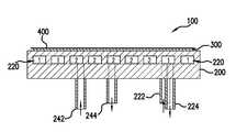
- an exemplary electrostatic chuck assembly 100includes metal pedestal support 200 and electrostatic chuck 300 .
- Pedestal support 200has a top surface for supporting electrostatic chuck 300 .
- the top surface or clamping surface 310 of electrostatic chuck 300supports substrate 400 during processing.
- Substrate 400can be a semiconductor wafer subjected to a plasma etch process, thermal process, or other process.
- the electrostatic chuck 300can be attached to the pedestal support 200 using an elastomeric adhesive.
- This adhesiveshould be thin to minimize stress generated from differential thermal expansion between the pedestal support 200 and the electrostatic chuck 300 .
- the adhesiveshould also ensure good thermal contact between the electrostatic chuck 300 and the pedestal support 200 .
- the adhesive layercan have a thermal conductivity of approximately 1.1 W/mK and a thickness of approximately 0.28 mm.
- the pedestal support 200can be made from a metal (e.g. aluminum) and includes a thermal control system for maintaining a substantially uniform temperature profile across the entire top surface of the pedestal support 200 .
- the thermal control systemprovides a pedestal thermal zone having thermal characteristics based on the output of the thermal control system. For instance, the thermal characteristics of the pedestal thermal zone can be varied by regulating the flow of a thermal exchange fluid through the pedestal or by regulating the temperature of a thermal exchange fluid flowing through the pedestal.
- the thermal control systemincludes two separate channels 220 , 240 for circulating a thermal exchange fluid through the pedestal.
- the two separate channels 220 , 240are operated at the same temperature to provide a uniform pedestal thermal zone.
- a variety of temperature control devicescan be used to maintain the temperature of the channels 220 , 240 at the same temperature.
- the two channels 220 , 240can be connected to either a single or dual heat exchange recirculation system that will control both channels to the same temperature.
- the use of two channels 220 , 240is preferred because, in certain embodiments, a single channel cannot extract enough heat. For instance, a single channel can be too long, causing the thermal properties of the liquid traveling through the single channel to change substantially before the liquid exits the channel.
- two channels maintained at a flow of, for example 3 GPMare easier to implement than one channel maintained at a flow of, for instance 6 GPM (i.e. smaller lines & connections).
- the pedestal support 200has two inputs 222 , 242 and two outputs 224 , 244 for circulating two streams of a thermal control liquid through the two separate channels 220 , 240 contained inside the pedestal body.
- the thermal control liquidcan be a water glycol mixture or other suitable thermal exchange liquid.
- electrostatic chuck 300includes clamping electrodes 320 and a plurality of independently controlled heating electrodes 330 .
- the clamping electrodes 320are used to generate an electrostatic clamping force for clamping a substrate 400 to the clamping surface 310 of the electrostatic chuck 300 .
- the heating electrodes 330are used to define a plurality of heating zones. Thermal characteristics of the heating zones are adjusted by controlling the output if the independently controlled heating electrodes 330 .
- the electrostatic chuck 300can be formed from a variety of materials, including a ceramic material.
- the electrostatic chuck materialhas a low thermal conductivity to maintain steep temperature gradients between adjacent thermal zones.
- the electrostatic chuckcan be formed from a ceramic material having a composition of approximately 94% Al 2 O 3 and 6% SiO 2 .
- the electrostatic chuck 300can be formed from multiple layers of green or partially fired ceramic with three or four layers of thin-film metal electrodes disposed between layers of ceramic.
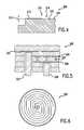
- FIG. 5depicts a multilayered ceramic electrostatic chuck 300 .
- the electrostatic chuck 300includes clamping electrode 320 disposed between two ceramic layers and heating electrodes 330 disposed between two different ceramic layers. All layers of ceramic and electrodes will undergo a final firing to form a finished electrostatic chuck 300 .
- final fabrication of the electrostatic chuck 300can involve forming a raised clamping surface 310 that comprises a raised peripheral ring 312 that will form an approximate seal with the bottom surface of a substrate 400 clamped to the clamping surface 310 of the electrostatic chuck 300 .
- the raised peripheral ring 312can have a height 313 of, for instance, 5 ⁇ m.
- the remaining clamping surface 310 of the electrostatic chuckcan contain a multitude of mesas 315 having a height equal to that of the peripheral ring 312 .
- the grooves 318allow for the flow of a heat transfer gas, for instance helium or other heat transfer gas, between the clamping surface 310 of the electrostatic chuck 300 and a substrate 400 mounted to the electrostatic chuck 300 .
- the electrostatic chuck 300can be a Johnsen-Rahbek electrostatic chuck or a Coulombic type electrostatic chuck 300 .
- a Johnsen-Rahbek electrostatic chuckcreates an electrostatic clamping force between the clamping surface 310 of the electrostatic chuck 300 and a substrate 400 .
- a Coulombic type electrostatic chuckcreates an electrostatic clamping force between the clamping electrodes 320 and a substrate 400 .
- the clamping electrodes 320can be fabricated of metal such as tungsten or other metal having a suitable coefficient of thermal expansion and electrical resistance properties and can be formed on the surface of a single layer of ceramic or on adjacent ceramic layers.
- the clamping electrodes 320can be formed using a deposition process such as screen printing, PVD, CVD, ALD, or plasma or arc spray.
- the electrostatic chuck 300includes a single post connection 325 for connecting the clamping electrodes to a power source.
- An exemplary pattern of clamping electrodes 320is depicted in FIG. 6 .
- the electrostatic chuck 300can be operated in either a bipolar or a monopolar configuration. For instance, in the case of a monopolar configuration, a single disc-shaped clamping electrode 320 is located between two ceramic layers. In the case of a bipolar configuration, two or more clamping electrodes 320 are located between two ceramic layers. If the two clamping electrodes are connected to voltage sources having opposite polarities, the electrostatic chuck 300 can be operated as a bipolar electrostatic chuck. If the two electrodes are connected to a common voltage source, the electrostatic chuck 300 operates can be operated as a monopolar device.
- the electrostatic chuck 300 shown in FIG. 3includes a plurality of independently controlled thin-film resistive heating electrodes 330 embedded within electrostatic chuck 300 .
- the heating electrodes 330can be fabricated of metal such as tungsten or other suitable metal and formed using a conventional deposition process such as screen printing, PVD, CVD, ALD, or plasma or arc spraying.
- Each heating electrode 330defines a heating zone having thermal characteristics based on the output of the heating electrodes 330 .
- the plurality of independently controlled heating electrodes 330includes an inner heating electrode 334 defining an inner heating zone and a peripheral heating electrode 332 defining a peripheral heating zone.
- the inner heating electrode 334defines a disc shaped heating zone located in the center of the electrostatic chuck 300 .
- the peripheral heating electrode 332defines a ring shaped heating zone surrounding the inner heating zone.
- the inner heating zone and the peripheral heating zoneare separated by a gap distance 335 .
- FIG. 7depicts an exemplary pattern of heating electrodes 330 according to one embodiment of the present disclosure.
- the thermal characteristics of the inner heating zone and the peripheral heating zonecan be adjusted by varying the output of the inner heating electrode and peripheral heating electrode respectively. For instance, the thermal characteristics of the inner heating zone can be varied by adjusting the amount of power supplied to the inner heating electrode 334 . Similarly, the thermal characteristics of the peripheral heating zone can be varied by adjusting the amount of power supplied to the peripheral heating electrode 332 .
- the capability of adjusting the thermal characteristics of the inner and peripheral heating zonesallows radial tuning of the temperature profile across the surface of the substrate. As shown in FIG. 5 , a heating electrode 330 can be connected to a power source through vias 337 , heating bus 336 and single post connection 338 .
- the temperature profile of the substratecan be measured using a variety of temperature measuring techniques. For instance, the temperature profile of the substrate can approximated by measuring the temperature profile of the electrostatic chuck at a location close to the top surface of the electrostatic chuck.
- reference to the temperature of a heating zonerefers to the temperature of the electrostatic chuck at a location in the heating zone close to the top surface of the electrostatic chuck.
- a fiber-optic temperature sensorcan be used to monitor temperature.
- a small disc containing a phosphoremits light having a predictable decay rate proportional to temperature.
- the phosphor coated discis located near the clamping surface 310 of the electrostatic chuck 300 so that the measurement serves as a good predictor of the temperature of the substrate 400 clamped to the clamping surface 310 of the electrostatic chuck 300 .
- a fiber-opticis located at a fixed distance from the phosphor coated disc to reliably capture light emitted by the phosphor.
- FIG. 8depicts a graphical representation of an exemplary desired temperature profile across the surface of a substrate.
- the peripheral edge of the substrate corresponding to the peripheral heating zonehas been tuned to achieve a higher temperature (T 2 ) than the temperature (T 1 ) of the central portion of the substrate corresponding to the inner heating zone.
- T 2the peripheral edge of the substrate corresponding to the peripheral heating zone
- T 1the temperature of the central portion of the substrate corresponding to the inner heating zone.
- An abrupt temperature gradientexists between the inner heating zone and the peripheral heating zone.
- the electrostatic chuck assembly of the present disclosurecan be used to tune the temperature gradient between the inner heating zone and the peripheral heating zone so that temperature gradient is steeper than gradients achieved by substrate holders known in the prior art.
- the temperature gradient between the inner heating zone and peripheral heating zonecan be tuned by varying the output of the pedestal thermal control system, the inner heating electrode, or the peripheral heating electrode.
- the applicantshave also discovered that the temperature gradient can be tuned by varying the size of the gap distance between the inner heating electrode and the peripheral heating electrode.
- a movable interface for varying the size of the gap distance between the inner heating electrode and peripheral heating electrodeis disclosed in FIG. 9 .
- the movable interfaceincludes additional heating electrodes 336 disposed between the inner heating electrode 334 and the peripheral heating electrode 332 .
- the size of the gap distance 335equals the distance between the inner heating electrode 334 and peripheral heating electrode 332 .
- the gap distanceadjusts from gap distance 335 to gap distance 335 ′.
- the size of gap distance 335 ′is the distance between the additional heating electrode and the peripheral or inner heating electrode and is smaller than the size of original gap distance 335 .
- the temperature gradient between the inner heating zone and the peripheral heating zonecan be tuned by adjusting the size of the gap distance between the inner heating electrode and the peripheral heating electrode. In this manner, an abrupt or steep temperature gradient between the inner heating zone and peripheral heating zone can be maintained.
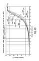
- FIGS. 10 and 11provide simulation results demonstrating the effect of changing the size of the gap distance between the inner heating zone and the peripheral heating zone on the temperature gradient between the inner heating zone and the peripheral heating zone.
- the peripheral heating zonewas maintained at a temperature approximately 28.5° C. higher than the temperature of the inner heating zone.
- FIGS. 10 and 11provide graphical representations of the temperature differences plotted as a function of distance from the center of the electrostatic chuck for electrostatic chuck assemblies having varying gap distances between the inner heating electrode and the peripheral heating electrode.
- the abruptness or steepness of the temperature gradientis dependent on the size of the gap distance between the inner heating electrode and peripheral heating electrode. More particularly, the temperature gradient varied from approximately 6° C./cm at a 2 mm gap to approximately 10° C./cm at a 35 mm gap.
- the temperature gradientwas measured by calculating the slope of the temperature difference curve plotted as a function of distance from the center of the substrate.
- the slopeis equal to the change in temperature difference divided by the change in distance for the middle 50% of the temperature difference curve according to the following formula:
- the results depicted in FIGS. 10 and 11indicate that the temperature gradient between the inner heating zone and peripheral heating zone is tunable based at least in part on the size of the gap distance between inner heating electrode and peripheral heating electrode.
- the temperature gradientcan also be tuned by varying the power supplied to the inner or peripheral heating electrodes.
- FIG. 12provides a graphical representation of the temperature difference at the substrate surface as a function of distance from the center of the substrate for electrostatic chuck assemblies having a gap distance of 20 mm at varying amounts of energy applied to the inner heating electrode.
- FIG. 12illustrates that by holding the gap fixed between adjacent electrodes and only changing the energy supplied to the inner electrode, the temperature gradient increases from approximately 8° C./cm at 1 W/cm 2 to approximately 13.5° C./cm at 3 W/cm 2 .
Landscapes
- Engineering & Computer Science (AREA)
- Power Engineering (AREA)
- Microelectronics & Electronic Packaging (AREA)
- General Physics & Mathematics (AREA)
- Manufacturing & Machinery (AREA)
- Computer Hardware Design (AREA)
- Physics & Mathematics (AREA)
- Condensed Matter Physics & Semiconductors (AREA)
- Mechanical Engineering (AREA)
- Container, Conveyance, Adherence, Positioning, Of Wafer (AREA)
- Drying Of Semiconductors (AREA)
- Physical Vapour Deposition (AREA)
- Chemical Vapour Deposition (AREA)
Abstract
Description
- This application claims the benefit of priority of U.S. Provisional Patent Application No. 61/149,876 filed on Feb. 4, 2009, which is incorporated by reference herein for all purposes.
- Various different types of processing chambers are available for processing different types of workpieces and substrates. The substrates can comprise, for instance, glass plates, films, ribbons, solar panels, mirrors, liquid crystal displays, semiconductor wafers, and the like. Many different types of processing chambers are available, for instance, for processing semiconductor wafers during the manufacture of integrated circuit chips. The processing chambers can be used to anneal the wafers, carry out chemical vapor deposition, plasma enhanced chemical vapor deposition, etching processes, and other deposition processes.
- The chamber typically includes a substrate holder, such as an electrostatic chuck assembly, to hold a substrate during processing. A typical electrostatic chuck includes one or more clamping electrodes covered by a dielectric layer. The clamping electrodes are used to generate an electrostatic clamping force for holding the substrate onto the top surface of the electrostatic chuck. Once a substrate is securely held onto a chuck, a process gas is introduced into a chamber and a plasma is formed to process the substrate. The substrate can be processed by a CVD, PVD, etch, implant, oxidation, nitridation or other process.
- In many processes, it is desirable to control the temperature of the substrate during processing. Processes can be optimized, for instance, if the temperature of the substrate is uniform and is increased and decreased at desired rates and to desired maximums and minimums. In some embodiments, it can be desired to divide the substrate into a plurality of heating zones with each heating zone being maintained at different temperatures to compensate for different heating effects across the surface of the substrate during processing of the substrate. For instance, a substrate can include an inner heating zone and a peripheral heating zone with the peripheral heating zone being maintained at a higher temperature than the inner heating zone to compensate for additional heat loss occurring at the periphery of the substrate. In circumstances when adjacent heating zones are maintained at different temperatures, it can be preferable to have an abrupt or steep temperature gradient between adjacent heating zones to more adequately compensate for the varying heating effects during processing.
- Thus, a need exists for an electrostatic chuck assembly that allows for the radial tuning or control of the temperature profile across the surface of the substrate and that provides an abrupt temperature gradient between adjacent heating zones.
- Aspects and advantages of the invention will be set forth in part in the following description, or may be obvious from the description, or may be learned through practice of the invention.
- One exemplary embodiment of the present disclosure provides an system for maintaining a temperature profile across the surface of the substrate. The system includes a pedestal support having a pedestal thermal control system adapted to provide a pedestal thermal zone having thermal characteristics based on the output of the pedestal thermal control system. The pedestal thermal zone defines a substantially uniform temperature profile across the surface of the pedestal support. The electrostatic chuck assembly further includes an electrostatic chuck supported by the pedestal support. The electrostatic chuck has a clamping electrode and a plurality of heating electrodes. The heating electrodes include an inner heating electrode and a peripheral heating electrode separated by a gap distance. The inner heating electrode defines an inner heating zone having thermal characteristics based on the output of the inner heating electrode. The peripheral heating electrode defines a peripheral heating zone having thermal characteristics based on the output of the peripheral heating electrode. The electrostatic chuck assembly includes a control system for adjusting the temperature profile across the surface of the substrate by varying at least one of the output of the pedestal thermal control system, the inner heating electrode, or the peripheral heating electrode.
- In a variation of this particular embodiment, the control system can be adapted to adjust the temperature gradient between the inner heating zone and the peripheral heating zone by varying the output of at least one of the pedestal thermal control system, inner heating electrode, or peripheral heating electrode.
- In other variations of this exemplary embodiment, the clamping electrode can be a monopolar electrode or a bipolar electrode. The electrostatic chuck assembly can also be comprised primarily of a ceramic material having a low thermal conductivity such as aluminum oxide. The top surface of the electrostatic chuck can include a raised peripheral seal ring and a plurality of mesas having a height approximately equal to the height of the raised peripheral seal ring.
- In yet another variation of this exemplary embodiment, the pedestal thermal control system can include a fluid flow channel for circulating a thermal exchange fluid. For instance, the thermal control system can include an inner fluid flow channel and a peripheral fluid flow channel being controlled to provide a substantially uniform temperature profile across the surface of the pedestal support. Thermal characteristics of the pedestal thermal zone can be varied by adjusting the output of the pedestal thermal control system, for instance, by regulating the temperature or flow of the fluid through the fluid flow channels.
- In still another variation of this exemplary embodiment, the electrostatic chuck includes an additional heating electrode between the inner heating electrode and peripheral heating electrode. The gap distance between the inner heating electrode and the peripheral heating electrode can be adjusted by energizing the additional heating electrode. The control system can be adapted to adjust the temperature gradient between the inner heating zone and peripheral heating zone by adjusting the size of the gap distance.
- Another exemplary embodiment of the present disclosure provides a system for maintaining a temperature profile across the surface of a substrate during processing. The system includes a pedestal defining a substantially uniform temperature profile across the surface of the pedestal and an electrostatic chuck having a clamping electrode and a plurality of heating electrodes. The heating electrodes include an inner heating electrode defining an inner heating zone and a peripheral heating electrode defining a peripheral heating zone. The inner heating electrode and the peripheral heating electrode are separated by a gap distance sufficient to create a temperature gradient between the peripheral heating zone and the inner heating zone. The temperature gradient is at least 6° C./cm when the temperature of the peripheral heating zone is maintained approximately 28.5° C. higher than the temperature of the inner heating zone. For instance, the temperature gradient can be at least 10° C./cm. In variations of this exemplary embodiment, the gap distance can be approximately 15 mm to 35 mm, such as approximately 18 mm to 30 mm, such as approximately 20 mm, or any other gap distance or range of gap distances therebetween.
- A further exemplary embodiment of the present disclosure provides a process for adjusting the temperature profile across the surface of a substrate. The process includes placing a substrate on an electrostatic chuck assembly that includes an electrostatic chuck supported by a pedestal. The electrostatic chuck includes a clamping electrode and an inner heating electrode defining an inner heating zone and a peripheral heating electrode defining a peripheral heating zone. The inner heating electrode and the peripheral heating electrode are separated by a gap distance. The process further includes clamping the substrate on the electrostatic chuck assembly by energizing the clamping electrode and tuning the temperature gradient between the inner heating zone and peripheral heating zone by varying the size of the gap distance between the inner heating electrode and the peripheral heating electrode.
- In a variation of this exemplary embodiment, the size of the gap distance between the inner heating electrode and the peripheral heating electrode can be varied by energizing an additional heating electrode disposed between the inner heating electrode and the outer heating electrode. In other variations of this exemplary embodiment, the temperature gradient between the inner heating zone and the peripheral heating zone can be adjusted by adjusting the power supplied to the inner heating electrode or the peripheral heating electrode, or by regulating the flow and temperature of heat transfer fluid through the pedestal.
- These and other features, aspects and advantages of the present invention will become better understood with reference to the following description and appended claims. The accompanying drawings, which are incorporated in and constitute a part of this specification, illustrate embodiments of the invention and, together with the description, serve to explain the principles of the invention.
- A full and enabling disclosure of the present invention, including the best mode thereof, directed to one of ordinary skill in the art, is set forth in the specification, which makes reference to the appended figures, in which:
FIG. 1 depicts a side view of an electrostatic chuck assembly according to an exemplary embodiment of the present disclosure;FIG. 2 depicts a plan view of an exemplary pedestal support according to an exemplary embodiment of the present disclosure;FIG. 3 depicts a side view of an electrostatic chuck assembly according to an exemplary embodiment of the present disclosure;FIG. 4 depicts an electrostatic chuck clamping surface according to an exemplary embodiment of the present disclosure;FIG. 5 depicts a layered electrostatic chuck according to an exemplary embodiment of the present disclosure;FIG. 6 depicts a plan view of an exemplary pattern of clamping electrodes according to an exemplary of the present disclosure;FIG. 7 depicts a plan view of an exemplary pattern of heating electrodes according to an exemplary of the present disclosure;FIG. 8 depicts a graphical representation of a temperature profile across the surface of a substrate according to an exemplary embodiment of the present disclosure;FIG. 9 depicts a heating electrode configuration providing a movable interface between the inner heating electrode and outer heating electrode according to an exemplary embodiment of the present disclosure;FIG. 10 depicts a graphical representation of the temperature difference of a substrate plotted as a function of distance from the center of the substrate for various gap distances;FIG. 11 depicts another graphical representation of the temperature difference of a substrate plotted as a function of distance from the center of the substrate for varying gap distances; andFIG. 12 depicts a graphical representation of the temperature difference of a substrate plotted as a function of distance from the center of the substrate for varying amounts of power applied to the inner electrode.- Reference now will be made in detail to embodiments of the invention, one or more examples of which are illustrated in the drawings. Each example is provided by way of explanation of the invention, not limitation of the invention. In fact, it will be apparent to those skilled in the art that various modifications and variations can be made in the present invention without departing from the scope or spirit of the invention. For instance, features illustrated or described as part of one embodiment, can be used with another embodiment to yield a still further embodiment. Thus, it is intended that the present invention covers such modifications and variations as come within the scope of the appended claims and their equivalents.
- Generally, the present disclosure is directed to an electrostatic chuck system and process for supporting a substrate and for maintaining a desired temperature profile across the surface of the substrate during processing. An example temperature profile is graphically represented in
FIG. 8 as a function of distance from the peripheral edge of the substrate. A temperature profile can also be graphically depicted as a function of distance from the center of the substrate. - The electrostatic chuck assembly of this exemplary embodiment can include a pedestal support having a pedestal thermal control system adapted to provide a pedestal thermal zone. The pedestal thermal zone defines a substantially uniform temperature profile across the surface of the pedestal support. The pedestal thermal zone has thermal characteristics based on the output of the pedestal thermal control system.
- The electrostatic chuck assembly can further include an electrostatic chuck supported by the pedestal support. The electrostatic chuck can have a clamping electrode and a plurality of independently controlled heating electrodes. The independently controlled heating electrodes include an inner heating electrode and a peripheral heating electrode. The inner heating electrode defines an inner heating zone having thermal characteristics based on the output of the inner heating electrode. The peripheral heating electrode defines a peripheral heating zone having thermal characteristics based on the output of the peripheral heating electrode.
- The inner heating electrode and the peripheral heating electrode can be separated by a gap distance. As used herein, the term gap distance refers to a space or gap between energized heating electrodes that has a distance. The gap distance preferably comprises a dielectric material of low thermal conductivity such as aluminum oxide. The gap distance can also comprise additional heating electrodes that have not been energized such as in the embodiment of the electrostatic chuck assembly having a moveable interface between heating electrodes. The size of the gap distance refers to the distance of separation between the energized heating electrodes.
- In certain embodiments, the electrostatic chuck assembly includes a control system adapted to radially tune or adjust the temperature profile across the surface of the substrate by varying the output of the pedestal thermal control system, the inner heating electrode, or the peripheral heating electrode. The control system can also be adapted to radially tune or adjust the temperature profile across the surface of the substrate by varying the size of the gap distance between the heating electrodes. The control system can include a single controller or multiple controllers for varying the output of the pedestal thermal control system, the inner heating electrode, or the peripheral heating electrode.
- The various heating zones of the electrostatic chuck can be maintained at different temperatures. For instance, the temperature of the peripheral heating zone can be maintained at a higher temperature than the temperature of the inner heating zone. In these circumstances, a temperature gradient exists between the inner heating zone and the peripheral heating zone. The temperature gradient refers to the amount the temperature of a substrate differs over a unit of length of the substrate. For instance, a temperature gradient of 6° C./cm indicates that the temperature varies by 6° C. over 1 cm length.
- The electrostatic chuck assembly according to embodiments of the present disclosure allows a user to adjust the temperature gradient between two heating zones by varying the thermal characteristics of at least one of the pedestal thermal zone, inner heating zone and/or peripheral heating zone or by adjusting the size of the gap distance between the inner heating zone and the peripheral heating zone. In this manner, the electrostatic chuck assembly according to embodiments of the present disclosure enhances the ability to obtain an desired temperature gradient on a substrate during processing.
- Referring now to
FIG. 1 , an exemplaryelectrostatic chuck assembly 100 includesmetal pedestal support 200 andelectrostatic chuck 300.Pedestal support 200 has a top surface for supportingelectrostatic chuck 300. The top surface or clampingsurface 310 ofelectrostatic chuck 300 supportssubstrate 400 during processing.Substrate 400 can be a semiconductor wafer subjected to a plasma etch process, thermal process, or other process. - The
electrostatic chuck 300 can be attached to thepedestal support 200 using an elastomeric adhesive. This adhesive should be thin to minimize stress generated from differential thermal expansion between thepedestal support 200 and theelectrostatic chuck 300. The adhesive should also ensure good thermal contact between theelectrostatic chuck 300 and thepedestal support 200. For instance, the adhesive layer can have a thermal conductivity of approximately 1.1 W/mK and a thickness of approximately 0.28 mm. - The
pedestal support 200 can be made from a metal (e.g. aluminum) and includes a thermal control system for maintaining a substantially uniform temperature profile across the entire top surface of thepedestal support 200. The thermal control system provides a pedestal thermal zone having thermal characteristics based on the output of the thermal control system. For instance, the thermal characteristics of the pedestal thermal zone can be varied by regulating the flow of a thermal exchange fluid through the pedestal or by regulating the temperature of a thermal exchange fluid flowing through the pedestal. - In
FIGS. 1 and 2 , the thermal control system includes twoseparate channels separate channels channels channels - The use of two
channels instance 6 GPM (i.e. smaller lines & connections). Thepedestal support 200 has twoinputs outputs separate channels - As shown in
FIG. 3 ,electrostatic chuck 300 includes clampingelectrodes 320 and a plurality of independently controlledheating electrodes 330. The clampingelectrodes 320 are used to generate an electrostatic clamping force for clamping asubstrate 400 to theclamping surface 310 of theelectrostatic chuck 300. Theheating electrodes 330 are used to define a plurality of heating zones. Thermal characteristics of the heating zones are adjusted by controlling the output if the independently controlledheating electrodes 330. - The
electrostatic chuck 300 can be formed from a variety of materials, including a ceramic material. Preferably, the electrostatic chuck material has a low thermal conductivity to maintain steep temperature gradients between adjacent thermal zones. For instance, the electrostatic chuck can be formed from a ceramic material having a composition of approximately 94% Al2O3and 6% SiO2. - The
electrostatic chuck 300 can be formed from multiple layers of green or partially fired ceramic with three or four layers of thin-film metal electrodes disposed between layers of ceramic. For instance,FIG. 5 depicts a multilayered ceramicelectrostatic chuck 300. Theelectrostatic chuck 300 includes clampingelectrode 320 disposed between two ceramic layers andheating electrodes 330 disposed between two different ceramic layers. All layers of ceramic and electrodes will undergo a final firing to form a finishedelectrostatic chuck 300. - As shown in
FIG. 4 , final fabrication of theelectrostatic chuck 300 can involve forming a raisedclamping surface 310 that comprises a raisedperipheral ring 312 that will form an approximate seal with the bottom surface of asubstrate 400 clamped to theclamping surface 310 of theelectrostatic chuck 300. The raisedperipheral ring 312 can have aheight 313 of, for instance, 5 μm. The remainingclamping surface 310 of the electrostatic chuck can contain a multitude ofmesas 315 having a height equal to that of theperipheral ring 312. Thegrooves 318 allow for the flow of a heat transfer gas, for instance helium or other heat transfer gas, between the clampingsurface 310 of theelectrostatic chuck 300 and asubstrate 400 mounted to theelectrostatic chuck 300. - The
electrostatic chuck 300 can be a Johnsen-Rahbek electrostatic chuck or a Coulombic typeelectrostatic chuck 300. A Johnsen-Rahbek electrostatic chuck creates an electrostatic clamping force between the clampingsurface 310 of theelectrostatic chuck 300 and asubstrate 400. A Coulombic type electrostatic chuck creates an electrostatic clamping force between the clampingelectrodes 320 and asubstrate 400. - The clamping
electrodes 320 can be fabricated of metal such as tungsten or other metal having a suitable coefficient of thermal expansion and electrical resistance properties and can be formed on the surface of a single layer of ceramic or on adjacent ceramic layers. The clampingelectrodes 320 can be formed using a deposition process such as screen printing, PVD, CVD, ALD, or plasma or arc spray. As shown inFIG. 5 , theelectrostatic chuck 300 includes asingle post connection 325 for connecting the clamping electrodes to a power source. An exemplary pattern of clampingelectrodes 320 is depicted inFIG. 6 . - The
electrostatic chuck 300 can be operated in either a bipolar or a monopolar configuration. For instance, in the case of a monopolar configuration, a single disc-shapedclamping electrode 320 is located between two ceramic layers. In the case of a bipolar configuration, two ormore clamping electrodes 320 are located between two ceramic layers. If the two clamping electrodes are connected to voltage sources having opposite polarities, theelectrostatic chuck 300 can be operated as a bipolar electrostatic chuck. If the two electrodes are connected to a common voltage source, theelectrostatic chuck 300 operates can be operated as a monopolar device. - The
electrostatic chuck 300 shown inFIG. 3 includes a plurality of independently controlled thin-filmresistive heating electrodes 330 embedded withinelectrostatic chuck 300. Theheating electrodes 330 can be fabricated of metal such as tungsten or other suitable metal and formed using a conventional deposition process such as screen printing, PVD, CVD, ALD, or plasma or arc spraying. Eachheating electrode 330 defines a heating zone having thermal characteristics based on the output of theheating electrodes 330. For instance, the plurality of independently controlledheating electrodes 330 includes aninner heating electrode 334 defining an inner heating zone and aperipheral heating electrode 332 defining a peripheral heating zone. Theinner heating electrode 334 defines a disc shaped heating zone located in the center of theelectrostatic chuck 300. Theperipheral heating electrode 332 defines a ring shaped heating zone surrounding the inner heating zone. The inner heating zone and the peripheral heating zone are separated by agap distance 335.FIG. 7 depicts an exemplary pattern ofheating electrodes 330 according to one embodiment of the present disclosure. - The thermal characteristics of the inner heating zone and the peripheral heating zone can be adjusted by varying the output of the inner heating electrode and peripheral heating electrode respectively. For instance, the thermal characteristics of the inner heating zone can be varied by adjusting the amount of power supplied to the
inner heating electrode 334. Similarly, the thermal characteristics of the peripheral heating zone can be varied by adjusting the amount of power supplied to theperipheral heating electrode 332. The capability of adjusting the thermal characteristics of the inner and peripheral heating zones allows radial tuning of the temperature profile across the surface of the substrate. As shown inFIG. 5 , aheating electrode 330 can be connected to a power source throughvias 337,heating bus 336 and single post connection338. - The temperature profile of the substrate can be measured using a variety of temperature measuring techniques. For instance, the temperature profile of the substrate can approximated by measuring the temperature profile of the electrostatic chuck at a location close to the top surface of the electrostatic chuck. Throughout the present disclosure, reference to the temperature of a heating zone refers to the temperature of the electrostatic chuck at a location in the heating zone close to the top surface of the electrostatic chuck.
- In one exemplary embodiment, a fiber-optic temperature sensor can be used to monitor temperature. In this embodiment, a small disc containing a phosphor emits light having a predictable decay rate proportional to temperature. The phosphor coated disc is located near the clamping
surface 310 of theelectrostatic chuck 300 so that the measurement serves as a good predictor of the temperature of thesubstrate 400 clamped to theclamping surface 310 of theelectrostatic chuck 300. A fiber-optic is located at a fixed distance from the phosphor coated disc to reliably capture light emitted by the phosphor. FIG. 8 depicts a graphical representation of an exemplary desired temperature profile across the surface of a substrate. As illustrated, the peripheral edge of the substrate corresponding to the peripheral heating zone has been tuned to achieve a higher temperature (T2) than the temperature (T1) of the central portion of the substrate corresponding to the inner heating zone. An abrupt temperature gradient exists between the inner heating zone and the peripheral heating zone.- The electrostatic chuck assembly of the present disclosure can be used to tune the temperature gradient between the inner heating zone and the peripheral heating zone so that temperature gradient is steeper than gradients achieved by substrate holders known in the prior art. For instance, the temperature gradient between the inner heating zone and peripheral heating zone can be tuned by varying the output of the pedestal thermal control system, the inner heating electrode, or the peripheral heating electrode. The applicants have also discovered that the temperature gradient can be tuned by varying the size of the gap distance between the inner heating electrode and the peripheral heating electrode.
- A movable interface for varying the size of the gap distance between the inner heating electrode and peripheral heating electrode is disclosed in
FIG. 9 . The movable interface includesadditional heating electrodes 336 disposed between theinner heating electrode 334 and theperipheral heating electrode 332. When none of theadditional heating electrodes 336 are energized, the size of thegap distance 335 equals the distance between theinner heating electrode 334 andperipheral heating electrode 332. However, if anadditional heating electrode 336 is energized, the gap distance adjusts fromgap distance 335 togap distance 335′. The size ofgap distance 335′ is the distance between the additional heating electrode and the peripheral or inner heating electrode and is smaller than the size oforiginal gap distance 335. Using this movable interface, the temperature gradient between the inner heating zone and the peripheral heating zone can be tuned by adjusting the size of the gap distance between the inner heating electrode and the peripheral heating electrode. In this manner, an abrupt or steep temperature gradient between the inner heating zone and peripheral heating zone can be maintained. - For example,
FIGS. 10 and 11 provide simulation results demonstrating the effect of changing the size of the gap distance between the inner heating zone and the peripheral heating zone on the temperature gradient between the inner heating zone and the peripheral heating zone. In performing the simulations, the peripheral heating zone was maintained at a temperature approximately 28.5° C. higher than the temperature of the inner heating zone.FIGS. 10 and 11 provide graphical representations of the temperature differences plotted as a function of distance from the center of the electrostatic chuck for electrostatic chuck assemblies having varying gap distances between the inner heating electrode and the peripheral heating electrode. As illustrated, the abruptness or steepness of the temperature gradient is dependent on the size of the gap distance between the inner heating electrode and peripheral heating electrode. More particularly, the temperature gradient varied from approximately 6° C./cm at a 2 mm gap to approximately 10° C./cm at a 35 mm gap. - In these examples, the temperature gradient was measured by calculating the slope of the temperature difference curve plotted as a function of distance from the center of the substrate. The slope is equal to the change in temperature difference divided by the change in distance for the middle 50% of the temperature difference curve according to the following formula:
- where T2=0.75Tmax; T1=0.25Tmax; d2=the distance from center at T2; d1=the distance from center at T1; and Tmaxis equal to the maximum temperature difference. The results depicted in
FIGS. 10 and 11 indicate that the temperature gradient between the inner heating zone and peripheral heating zone is tunable based at least in part on the size of the gap distance between inner heating electrode and peripheral heating electrode. - The temperature gradient can also be tuned by varying the power supplied to the inner or peripheral heating electrodes.
FIG. 12 provides a graphical representation of the temperature difference at the substrate surface as a function of distance from the center of the substrate for electrostatic chuck assemblies having a gap distance of 20 mm at varying amounts of energy applied to the inner heating electrode.FIG. 12 illustrates that by holding the gap fixed between adjacent electrodes and only changing the energy supplied to the inner electrode, the temperature gradient increases from approximately 8° C./cm at 1 W/cm2to approximately 13.5° C./cm at 3 W/cm2. - While the present subject matter has been described in detail with respect to specific exemplary embodiments and methods thereof, it will be appreciated that those skilled in the art, upon attaining an understanding of the foregoing can readily produce alterations to, variations of, and equivalents to such embodiments. Accordingly, the scope of the present disclosure is by way of example rather than by way of limitation, and the subject disclosure does not preclude inclusion of such modifications, variations and/or additions to the present subject matter as would be readily apparent to one of ordinary skill in the art.
Claims (20)
Priority Applications (1)
| Application Number | Priority Date | Filing Date | Title |
|---|---|---|---|
| US12/696,119US8405005B2 (en) | 2009-02-04 | 2010-01-29 | Electrostatic chuck system and process for radially tuning the temperature profile across the surface of a substrate |
Applications Claiming Priority (2)
| Application Number | Priority Date | Filing Date | Title |
|---|---|---|---|
| US14987609P | 2009-02-04 | 2009-02-04 | |
| US12/696,119US8405005B2 (en) | 2009-02-04 | 2010-01-29 | Electrostatic chuck system and process for radially tuning the temperature profile across the surface of a substrate |
Publications (2)
| Publication Number | Publication Date |
|---|---|
| US20100193501A1true US20100193501A1 (en) | 2010-08-05 |
| US8405005B2 US8405005B2 (en) | 2013-03-26 |
Family
ID=41718915
Family Applications (1)
| Application Number | Title | Priority Date | Filing Date |
|---|---|---|---|
| US12/696,119Active2031-03-18US8405005B2 (en) | 2009-02-04 | 2010-01-29 | Electrostatic chuck system and process for radially tuning the temperature profile across the surface of a substrate |
Country Status (6)
| Country | Link |
|---|---|
| US (1) | US8405005B2 (en) |
| JP (2) | JP5705133B2 (en) |
| KR (1) | KR101691044B1 (en) |
| CN (1) | CN102308380B (en) |
| TW (1) | TWI576951B (en) |
| WO (1) | WO2010090948A1 (en) |
Cited By (428)
| Publication number | Priority date | Publication date | Assignee | Title |
|---|---|---|---|---|
| US20120147353A1 (en)* | 2010-12-14 | 2012-06-14 | Asml Netherlands B.V. | Substrate holder, lithographic apparatus, device manufacturing method, and method of manufacturing a substrate holder |
| US20130230814A1 (en)* | 2012-03-02 | 2013-09-05 | Asm Ip Holding B.V. | Susceptor heater shim |
| WO2013162938A1 (en)* | 2012-04-25 | 2013-10-31 | Applied Materials, Inc. | Esc cooling base for large diameter substrates |
| WO2014116392A1 (en)* | 2013-01-25 | 2014-07-31 | Applied Materials, Inc. | Electrostatic chuck with concentric cooling base |
| US8877655B2 (en) | 2010-05-07 | 2014-11-04 | Asm America, Inc. | Systems and methods for thin-film deposition of metal oxides using excited nitrogen-oxygen species |
| US8883270B2 (en) | 2009-08-14 | 2014-11-11 | Asm America, Inc. | Systems and methods for thin-film deposition of metal oxides using excited nitrogen—oxygen species |
| US8894870B2 (en) | 2013-02-01 | 2014-11-25 | Asm Ip Holding B.V. | Multi-step method and apparatus for etching compounds containing a metal |
| US8933375B2 (en) | 2012-06-27 | 2015-01-13 | Asm Ip Holding B.V. | Susceptor heater and method of heating a substrate |
| US8946830B2 (en) | 2012-04-04 | 2015-02-03 | Asm Ip Holdings B.V. | Metal oxide protective layer for a semiconductor device |
| US8986456B2 (en) | 2006-10-10 | 2015-03-24 | Asm America, Inc. | Precursor delivery system |
| JPWO2013047555A1 (en)* | 2011-09-28 | 2015-03-26 | 住友大阪セメント株式会社 | Electrostatic chuck device |
| US8993054B2 (en) | 2013-07-12 | 2015-03-31 | Asm Ip Holding B.V. | Method and system to reduce outgassing in a reaction chamber |
| US9005539B2 (en) | 2011-11-23 | 2015-04-14 | Asm Ip Holding B.V. | Chamber sealing member |
| US9018111B2 (en) | 2013-07-22 | 2015-04-28 | Asm Ip Holding B.V. | Semiconductor reaction chamber with plasma capabilities |
| US9017481B1 (en) | 2011-10-28 | 2015-04-28 | Asm America, Inc. | Process feed management for semiconductor substrate processing |
| US9021985B2 (en) | 2012-09-12 | 2015-05-05 | Asm Ip Holdings B.V. | Process gas management for an inductively-coupled plasma deposition reactor |
| US9029253B2 (en) | 2012-05-02 | 2015-05-12 | Asm Ip Holding B.V. | Phase-stabilized thin films, structures and devices including the thin films, and methods of forming same |
| US9096931B2 (en) | 2011-10-27 | 2015-08-04 | Asm America, Inc | Deposition valve assembly and method of heating the same |
| US9117866B2 (en) | 2012-07-31 | 2015-08-25 | Asm Ip Holding B.V. | Apparatus and method for calculating a wafer position in a processing chamber under process conditions |
| US9167625B2 (en) | 2011-11-23 | 2015-10-20 | Asm Ip Holding B.V. | Radiation shielding for a substrate holder |
| US9169975B2 (en) | 2012-08-28 | 2015-10-27 | Asm Ip Holding B.V. | Systems and methods for mass flow controller verification |
| US9177784B2 (en) | 2012-05-07 | 2015-11-03 | Asm Ip Holdings B.V. | Semiconductor device dielectric interface layer |
| US9240412B2 (en) | 2013-09-27 | 2016-01-19 | Asm Ip Holding B.V. | Semiconductor structure and device and methods of forming same using selective epitaxial process |
| US9256139B2 (en) | 2011-02-18 | 2016-02-09 | Asml Netherlands B.V. | Substrate holder, lithographic apparatus, device manufacturing method, and method of manufacturing a substrate holder |
| US20160083840A1 (en)* | 2014-09-24 | 2016-03-24 | Applied Materials, Inc. | Graphite susceptor |
| US9324811B2 (en) | 2012-09-26 | 2016-04-26 | Asm Ip Holding B.V. | Structures and devices including a tensile-stressed silicon arsenic layer and methods of forming same |
| US9341296B2 (en) | 2011-10-27 | 2016-05-17 | Asm America, Inc. | Heater jacket for a fluid line |
| US9354528B2 (en) | 2011-04-27 | 2016-05-31 | Asml Netherlands B.V. | Substrate holder, lithographic apparatus, device manufacturing method, and method of manufacturing a substrate holder |
| WO2016085826A1 (en)* | 2014-11-26 | 2016-06-02 | Applied Materials, Inc. | Substrate carrier using a proportional thermal fluid delivery system |
| US9396934B2 (en) | 2013-08-14 | 2016-07-19 | Asm Ip Holding B.V. | Methods of forming films including germanium tin and structures and devices including the films |
| US9394608B2 (en) | 2009-04-06 | 2016-07-19 | Asm America, Inc. | Semiconductor processing reactor and components thereof |
| US9404587B2 (en) | 2014-04-24 | 2016-08-02 | ASM IP Holding B.V | Lockout tagout for semiconductor vacuum valve |
| US9442395B2 (en) | 2012-02-03 | 2016-09-13 | Asml Netherlands B.V. | Substrate holder, lithographic apparatus, device manufacturing method, and method of manufacturing a substrate holder |
| US9447498B2 (en) | 2014-03-18 | 2016-09-20 | Asm Ip Holding B.V. | Method for performing uniform processing in gas system-sharing multiple reaction chambers |
| US9455138B1 (en) | 2015-11-10 | 2016-09-27 | Asm Ip Holding B.V. | Method for forming dielectric film in trenches by PEALD using H-containing gas |
| US9478415B2 (en) | 2015-02-13 | 2016-10-25 | Asm Ip Holding B.V. | Method for forming film having low resistance and shallow junction depth |
| US9484191B2 (en) | 2013-03-08 | 2016-11-01 | Asm Ip Holding B.V. | Pulsed remote plasma method and system |
| WO2016190905A1 (en)* | 2015-05-22 | 2016-12-01 | Applied Materials, Inc. | Azimuthally tunable multi-zone electrostatic chuck |
| US9543180B2 (en) | 2014-08-01 | 2017-01-10 | Asm Ip Holding B.V. | Apparatus and method for transporting wafers between wafer carrier and process tool under vacuum |
| US9556516B2 (en) | 2013-10-09 | 2017-01-31 | ASM IP Holding B.V | Method for forming Ti-containing film by PEALD using TDMAT or TDEAT |
| US9558931B2 (en) | 2012-07-27 | 2017-01-31 | Asm Ip Holding B.V. | System and method for gas-phase sulfur passivation of a semiconductor surface |
| US9589770B2 (en) | 2013-03-08 | 2017-03-07 | Asm Ip Holding B.V. | Method and systems for in-situ formation of intermediate reactive species |
| US9605343B2 (en) | 2013-11-13 | 2017-03-28 | Asm Ip Holding B.V. | Method for forming conformal carbon films, structures conformal carbon film, and system of forming same |
| US9607837B1 (en) | 2015-12-21 | 2017-03-28 | Asm Ip Holding B.V. | Method for forming silicon oxide cap layer for solid state diffusion process |
| US9627221B1 (en) | 2015-12-28 | 2017-04-18 | Asm Ip Holding B.V. | Continuous process incorporating atomic layer etching |
| US9640416B2 (en) | 2012-12-26 | 2017-05-02 | Asm Ip Holding B.V. | Single-and dual-chamber module-attachable wafer-handling chamber |
| US9647114B2 (en) | 2015-08-14 | 2017-05-09 | Asm Ip Holding B.V. | Methods of forming highly p-type doped germanium tin films and structures and devices including the films |
| US20170133244A1 (en)* | 2015-11-11 | 2017-05-11 | Applied Materials, Inc. | Cooling base with spiral channels for esc |
| US9659799B2 (en) | 2012-08-28 | 2017-05-23 | Asm Ip Holding B.V. | Systems and methods for dynamic semiconductor process scheduling |
| US9657845B2 (en) | 2014-10-07 | 2017-05-23 | Asm Ip Holding B.V. | Variable conductance gas distribution apparatus and method |
| US9711345B2 (en) | 2015-08-25 | 2017-07-18 | Asm Ip Holding B.V. | Method for forming aluminum nitride-based film by PEALD |
| US9735024B2 (en) | 2015-12-28 | 2017-08-15 | Asm Ip Holding B.V. | Method of atomic layer etching using functional group-containing fluorocarbon |
| US9754779B1 (en) | 2016-02-19 | 2017-09-05 | Asm Ip Holding B.V. | Method for forming silicon nitride film selectively on sidewalls or flat surfaces of trenches |
| US9793135B1 (en) | 2016-07-14 | 2017-10-17 | ASM IP Holding B.V | Method of cyclic dry etching using etchant film |
| US9793148B2 (en) | 2011-06-22 | 2017-10-17 | Asm Japan K.K. | Method for positioning wafers in multiple wafer transport |
| US9793115B2 (en) | 2013-08-14 | 2017-10-17 | Asm Ip Holding B.V. | Structures and devices including germanium-tin films and methods of forming same |
| US9812320B1 (en) | 2016-07-28 | 2017-11-07 | Asm Ip Holding B.V. | Method and apparatus for filling a gap |
| US9859151B1 (en) | 2016-07-08 | 2018-01-02 | Asm Ip Holding B.V. | Selective film deposition method to form air gaps |
| US9887082B1 (en) | 2016-07-28 | 2018-02-06 | Asm Ip Holding B.V. | Method and apparatus for filling a gap |
| US9890456B2 (en) | 2014-08-21 | 2018-02-13 | Asm Ip Holding B.V. | Method and system for in situ formation of gas-phase compounds |
| US9891521B2 (en) | 2014-11-19 | 2018-02-13 | Asm Ip Holding B.V. | Method for depositing thin film |
| US9899291B2 (en) | 2015-07-13 | 2018-02-20 | Asm Ip Holding B.V. | Method for protecting layer by forming hydrocarbon-based extremely thin film |
| US9899405B2 (en) | 2014-12-22 | 2018-02-20 | Asm Ip Holding B.V. | Semiconductor device and manufacturing method thereof |
| US9905420B2 (en) | 2015-12-01 | 2018-02-27 | Asm Ip Holding B.V. | Methods of forming silicon germanium tin films and structures and devices including the films |
| US9909214B2 (en) | 2015-10-15 | 2018-03-06 | Asm Ip Holding B.V. | Method for depositing dielectric film in trenches by PEALD |
| US9916980B1 (en) | 2016-12-15 | 2018-03-13 | Asm Ip Holding B.V. | Method of forming a structure on a substrate |
| US9960072B2 (en) | 2015-09-29 | 2018-05-01 | Asm Ip Holding B.V. | Variable adjustment for precise matching of multiple chamber cavity housings |
| US10032628B2 (en) | 2016-05-02 | 2018-07-24 | Asm Ip Holding B.V. | Source/drain performance through conformal solid state doping |
| US10043661B2 (en) | 2015-07-13 | 2018-08-07 | Asm Ip Holding B.V. | Method for protecting layer by forming hydrocarbon-based extremely thin film |
| CN108550544A (en)* | 2013-05-07 | 2018-09-18 | 应用材料公司 | Electrostatic chuck with the thermal isolation area containing minimum crosstalk |
| US10083836B2 (en) | 2015-07-24 | 2018-09-25 | Asm Ip Holding B.V. | Formation of boron-doped titanium metal films with high work function |
| US10087525B2 (en) | 2015-08-04 | 2018-10-02 | Asm Ip Holding B.V. | Variable gap hard stop design |
| US10087522B2 (en) | 2016-04-21 | 2018-10-02 | Asm Ip Holding B.V. | Deposition of metal borides |
| US10090316B2 (en) | 2016-09-01 | 2018-10-02 | Asm Ip Holding B.V. | 3D stacked multilayer semiconductor memory using doped select transistor channel |
| USD830981S1 (en) | 2017-04-07 | 2018-10-16 | Asm Ip Holding B.V. | Susceptor for semiconductor substrate processing apparatus |
| US10103040B1 (en) | 2017-03-31 | 2018-10-16 | Asm Ip Holding B.V. | Apparatus and method for manufacturing a semiconductor device |
| US10134757B2 (en) | 2016-11-07 | 2018-11-20 | Asm Ip Holding B.V. | Method of processing a substrate and a device manufactured by using the method |
| US10167557B2 (en) | 2014-03-18 | 2019-01-01 | Asm Ip Holding B.V. | Gas distribution system, reactor including the system, and methods of using the same |
| US10177025B2 (en) | 2016-07-28 | 2019-01-08 | Asm Ip Holding B.V. | Method and apparatus for filling a gap |
| US10179947B2 (en) | 2013-11-26 | 2019-01-15 | Asm Ip Holding B.V. | Method for forming conformal nitrided, oxidized, or carbonized dielectric film by atomic layer deposition |
| US10190213B2 (en) | 2016-04-21 | 2019-01-29 | Asm Ip Holding B.V. | Deposition of metal borides |
| US10211308B2 (en) | 2015-10-21 | 2019-02-19 | Asm Ip Holding B.V. | NbMC layers |
| US10229833B2 (en) | 2016-11-01 | 2019-03-12 | Asm Ip Holding B.V. | Methods for forming a transition metal nitride film on a substrate by atomic layer deposition and related semiconductor device structures |
| US10236177B1 (en) | 2017-08-22 | 2019-03-19 | ASM IP Holding B.V.. | Methods for depositing a doped germanium tin semiconductor and related semiconductor device structures |
| US10249524B2 (en) | 2017-08-09 | 2019-04-02 | Asm Ip Holding B.V. | Cassette holder assembly for a substrate cassette and holding member for use in such assembly |
| US10249577B2 (en) | 2016-05-17 | 2019-04-02 | Asm Ip Holding B.V. | Method of forming metal interconnection and method of fabricating semiconductor apparatus using the method |
| US10262859B2 (en) | 2016-03-24 | 2019-04-16 | Asm Ip Holding B.V. | Process for forming a film on a substrate using multi-port injection assemblies |
| US10269558B2 (en) | 2016-12-22 | 2019-04-23 | Asm Ip Holding B.V. | Method of forming a structure on a substrate |
| US10276355B2 (en) | 2015-03-12 | 2019-04-30 | Asm Ip Holding B.V. | Multi-zone reactor, system including the reactor, and method of using the same |
| US10283353B2 (en) | 2017-03-29 | 2019-05-07 | Asm Ip Holding B.V. | Method of reforming insulating film deposited on substrate with recess pattern |
| US10290508B1 (en) | 2017-12-05 | 2019-05-14 | Asm Ip Holding B.V. | Method for forming vertical spacers for spacer-defined patterning |
| US10312055B2 (en) | 2017-07-26 | 2019-06-04 | Asm Ip Holding B.V. | Method of depositing film by PEALD using negative bias |
| US10319588B2 (en) | 2017-10-10 | 2019-06-11 | Asm Ip Holding B.V. | Method for depositing a metal chalcogenide on a substrate by cyclical deposition |
| US10322384B2 (en) | 2015-11-09 | 2019-06-18 | Asm Ip Holding B.V. | Counter flow mixer for process chamber |
| US10340135B2 (en) | 2016-11-28 | 2019-07-02 | Asm Ip Holding B.V. | Method of topologically restricted plasma-enhanced cyclic deposition of silicon or metal nitride |
| US10343920B2 (en) | 2016-03-18 | 2019-07-09 | Asm Ip Holding B.V. | Aligned carbon nanotubes |
| US10367080B2 (en) | 2016-05-02 | 2019-07-30 | Asm Ip Holding B.V. | Method of forming a germanium oxynitride film |
| US10364496B2 (en) | 2011-06-27 | 2019-07-30 | Asm Ip Holding B.V. | Dual section module having shared and unshared mass flow controllers |
| US10381226B2 (en) | 2016-07-27 | 2019-08-13 | Asm Ip Holding B.V. | Method of processing substrate |
| US10378106B2 (en) | 2008-11-14 | 2019-08-13 | Asm Ip Holding B.V. | Method of forming insulation film by modified PEALD |
| US10381219B1 (en) | 2018-10-25 | 2019-08-13 | Asm Ip Holding B.V. | Methods for forming a silicon nitride film |
| US10388513B1 (en) | 2018-07-03 | 2019-08-20 | Asm Ip Holding B.V. | Method for depositing silicon-free carbon-containing film as gap-fill layer by pulse plasma-assisted deposition |
| US10388509B2 (en) | 2016-06-28 | 2019-08-20 | Asm Ip Holding B.V. | Formation of epitaxial layers via dislocation filtering |
| US10395919B2 (en) | 2016-07-28 | 2019-08-27 | Asm Ip Holding B.V. | Method and apparatus for filling a gap |
| US10403504B2 (en) | 2017-10-05 | 2019-09-03 | Asm Ip Holding B.V. | Method for selectively depositing a metallic film on a substrate |
| US10410943B2 (en) | 2016-10-13 | 2019-09-10 | Asm Ip Holding B.V. | Method for passivating a surface of a semiconductor and related systems |
| US10435790B2 (en) | 2016-11-01 | 2019-10-08 | Asm Ip Holding B.V. | Method of subatmospheric plasma-enhanced ALD using capacitively coupled electrodes with narrow gap |
| US10446393B2 (en) | 2017-05-08 | 2019-10-15 | Asm Ip Holding B.V. | Methods for forming silicon-containing epitaxial layers and related semiconductor device structures |
| US10458018B2 (en) | 2015-06-26 | 2019-10-29 | Asm Ip Holding B.V. | Structures including metal carbide material, devices including the structures, and methods of forming same |
| US10468262B2 (en) | 2017-02-15 | 2019-11-05 | Asm Ip Holding B.V. | Methods for forming a metallic film on a substrate by a cyclical deposition and related semiconductor device structures |
| US10468251B2 (en) | 2016-02-19 | 2019-11-05 | Asm Ip Holding B.V. | Method for forming spacers using silicon nitride film for spacer-defined multiple patterning |
| US10483099B1 (en) | 2018-07-26 | 2019-11-19 | Asm Ip Holding B.V. | Method for forming thermally stable organosilicon polymer film |
| US10501866B2 (en) | 2016-03-09 | 2019-12-10 | Asm Ip Holding B.V. | Gas distribution apparatus for improved film uniformity in an epitaxial system |
| US10504742B2 (en) | 2017-05-31 | 2019-12-10 | Asm Ip Holding B.V. | Method of atomic layer etching using hydrogen plasma |
| US10510536B2 (en) | 2018-03-29 | 2019-12-17 | Asm Ip Holding B.V. | Method of depositing a co-doped polysilicon film on a surface of a substrate within a reaction chamber |
| US10529554B2 (en) | 2016-02-19 | 2020-01-07 | Asm Ip Holding B.V. | Method for forming silicon nitride film selectively on sidewalls or flat surfaces of trenches |
| US10529542B2 (en) | 2015-03-11 | 2020-01-07 | Asm Ip Holdings B.V. | Cross-flow reactor and method |
| US10529563B2 (en) | 2017-03-29 | 2020-01-07 | Asm Ip Holdings B.V. | Method for forming doped metal oxide films on a substrate by cyclical deposition and related semiconductor device structures |
| US10535516B2 (en) | 2018-02-01 | 2020-01-14 | Asm Ip Holdings B.V. | Method for depositing a semiconductor structure on a surface of a substrate and related semiconductor structures |
| US10541333B2 (en) | 2017-07-19 | 2020-01-21 | Asm Ip Holding B.V. | Method for depositing a group IV semiconductor and related semiconductor device structures |
| US10559458B1 (en) | 2018-11-26 | 2020-02-11 | Asm Ip Holding B.V. | Method of forming oxynitride film |
| US10590535B2 (en) | 2017-07-26 | 2020-03-17 | Asm Ip Holdings B.V. | Chemical treatment, deposition and/or infiltration apparatus and method for using the same |
| US10600673B2 (en) | 2015-07-07 | 2020-03-24 | Asm Ip Holding B.V. | Magnetic susceptor to baseplate seal |
| US10607895B2 (en) | 2017-09-18 | 2020-03-31 | Asm Ip Holdings B.V. | Method for forming a semiconductor device structure comprising a gate fill metal |
| US10605530B2 (en) | 2017-07-26 | 2020-03-31 | Asm Ip Holding B.V. | Assembly of a liner and a flange for a vertical furnace as well as the liner and the vertical furnace |
| US10612136B2 (en) | 2018-06-29 | 2020-04-07 | ASM IP Holding, B.V. | Temperature-controlled flange and reactor system including same |
| US10612137B2 (en) | 2016-07-08 | 2020-04-07 | Asm Ip Holdings B.V. | Organic reactants for atomic layer deposition |
| USD880437S1 (en) | 2018-02-01 | 2020-04-07 | Asm Ip Holding B.V. | Gas supply plate for semiconductor manufacturing apparatus |
| US10643904B2 (en) | 2016-11-01 | 2020-05-05 | Asm Ip Holdings B.V. | Methods for forming a semiconductor device and related semiconductor device structures |
| US10643826B2 (en) | 2016-10-26 | 2020-05-05 | Asm Ip Holdings B.V. | Methods for thermally calibrating reaction chambers |
| US10655221B2 (en) | 2017-02-09 | 2020-05-19 | Asm Ip Holding B.V. | Method for depositing oxide film by thermal ALD and PEALD |
| US10658181B2 (en) | 2018-02-20 | 2020-05-19 | Asm Ip Holding B.V. | Method of spacer-defined direct patterning in semiconductor fabrication |
| US10658205B2 (en) | 2017-09-28 | 2020-05-19 | Asm Ip Holdings B.V. | Chemical dispensing apparatus and methods for dispensing a chemical to a reaction chamber |
| US10685834B2 (en) | 2017-07-05 | 2020-06-16 | Asm Ip Holdings B.V. | Methods for forming a silicon germanium tin layer and related semiconductor device structures |
| US10683571B2 (en) | 2014-02-25 | 2020-06-16 | Asm Ip Holding B.V. | Gas supply manifold and method of supplying gases to chamber using same |
| US10692741B2 (en) | 2017-08-08 | 2020-06-23 | Asm Ip Holdings B.V. | Radiation shield |
| US10707106B2 (en) | 2011-06-06 | 2020-07-07 | Asm Ip Holding B.V. | High-throughput semiconductor-processing apparatus equipped with multiple dual-chamber modules |
| US10714315B2 (en) | 2012-10-12 | 2020-07-14 | Asm Ip Holdings B.V. | Semiconductor reaction chamber showerhead |
| US10714350B2 (en) | 2016-11-01 | 2020-07-14 | ASM IP Holdings, B.V. | Methods for forming a transition metal niobium nitride film on a substrate by atomic layer deposition and related semiconductor device structures |
| US10714385B2 (en) | 2016-07-19 | 2020-07-14 | Asm Ip Holding B.V. | Selective deposition of tungsten |
| US10714335B2 (en) | 2017-04-25 | 2020-07-14 | Asm Ip Holding B.V. | Method of depositing thin film and method of manufacturing semiconductor device |
| US10731249B2 (en) | 2018-02-15 | 2020-08-04 | Asm Ip Holding B.V. | Method of forming a transition metal containing film on a substrate by a cyclical deposition process, a method for supplying a transition metal halide compound to a reaction chamber, and related vapor deposition apparatus |
| US10734497B2 (en) | 2017-07-18 | 2020-08-04 | Asm Ip Holding B.V. | Methods for forming a semiconductor device structure and related semiconductor device structures |
| US10734244B2 (en) | 2017-11-16 | 2020-08-04 | Asm Ip Holding B.V. | Method of processing a substrate and a device manufactured by the same |
| US10755922B2 (en) | 2018-07-03 | 2020-08-25 | Asm Ip Holding B.V. | Method for depositing silicon-free carbon-containing film as gap-fill layer by pulse plasma-assisted deposition |
| US10767789B2 (en) | 2018-07-16 | 2020-09-08 | Asm Ip Holding B.V. | Diaphragm valves, valve components, and methods for forming valve components |
| US10770286B2 (en) | 2017-05-08 | 2020-09-08 | Asm Ip Holdings B.V. | Methods for selectively forming a silicon nitride film on a substrate and related semiconductor device structures |
| US10770336B2 (en) | 2017-08-08 | 2020-09-08 | Asm Ip Holding B.V. | Substrate lift mechanism and reactor including same |
| US10797133B2 (en) | 2018-06-21 | 2020-10-06 | Asm Ip Holding B.V. | Method for depositing a phosphorus doped silicon arsenide film and related semiconductor device structures |
| CN111755375A (en)* | 2019-03-26 | 2020-10-09 | 日本碍子株式会社 | Wafer carrying device |
| US10804098B2 (en) | 2009-08-14 | 2020-10-13 | Asm Ip Holding B.V. | Systems and methods for thin-film deposition of metal oxides using excited nitrogen-oxygen species |
| US10811256B2 (en) | 2018-10-16 | 2020-10-20 | Asm Ip Holding B.V. | Method for etching a carbon-containing feature |
| US10811301B2 (en)* | 2015-02-09 | 2020-10-20 | Applied Materials, Inc. | Dual-zone heater for plasma processing |
| US10818758B2 (en) | 2018-11-16 | 2020-10-27 | Asm Ip Holding B.V. | Methods for forming a metal silicate film on a substrate in a reaction chamber and related semiconductor device structures |
| USD900036S1 (en) | 2017-08-24 | 2020-10-27 | Asm Ip Holding B.V. | Heater electrical connector and adapter |
| US10829852B2 (en) | 2018-08-16 | 2020-11-10 | Asm Ip Holding B.V. | Gas distribution device for a wafer processing apparatus |
| US10844484B2 (en) | 2017-09-22 | 2020-11-24 | Asm Ip Holding B.V. | Apparatus for dispensing a vapor phase reactant to a reaction chamber and related methods |
| US10847371B2 (en) | 2018-03-27 | 2020-11-24 | Asm Ip Holding B.V. | Method of forming an electrode on a substrate and a semiconductor device structure including an electrode |
| US10847366B2 (en) | 2018-11-16 | 2020-11-24 | Asm Ip Holding B.V. | Methods for depositing a transition metal chalcogenide film on a substrate by a cyclical deposition process |
| US10847365B2 (en) | 2018-10-11 | 2020-11-24 | Asm Ip Holding B.V. | Method of forming conformal silicon carbide film by cyclic CVD |
| US10854498B2 (en) | 2011-07-15 | 2020-12-01 | Asm Ip Holding B.V. | Wafer-supporting device and method for producing same |
| USD903477S1 (en) | 2018-01-24 | 2020-12-01 | Asm Ip Holdings B.V. | Metal clamp |
| US10858737B2 (en) | 2014-07-28 | 2020-12-08 | Asm Ip Holding B.V. | Showerhead assembly and components thereof |
| US10867788B2 (en) | 2016-12-28 | 2020-12-15 | Asm Ip Holding B.V. | Method of forming a structure on a substrate |
| US10865475B2 (en) | 2016-04-21 | 2020-12-15 | Asm Ip Holding B.V. | Deposition of metal borides and silicides |
| US10867786B2 (en) | 2018-03-30 | 2020-12-15 | Asm Ip Holding B.V. | Substrate processing method |
| US10872771B2 (en) | 2018-01-16 | 2020-12-22 | Asm Ip Holding B. V. | Method for depositing a material film on a substrate within a reaction chamber by a cyclical deposition process and related device structures |
| US10886123B2 (en) | 2017-06-02 | 2021-01-05 | Asm Ip Holding B.V. | Methods for forming low temperature semiconductor layers and related semiconductor device structures |
| US10883175B2 (en) | 2018-08-09 | 2021-01-05 | Asm Ip Holding B.V. | Vertical furnace for processing substrates and a liner for use therein |
| US10892156B2 (en) | 2017-05-08 | 2021-01-12 | Asm Ip Holding B.V. | Methods for forming a silicon nitride film on a substrate and related semiconductor device structures |
| US10896820B2 (en) | 2018-02-14 | 2021-01-19 | Asm Ip Holding B.V. | Method for depositing a ruthenium-containing film on a substrate by a cyclical deposition process |
| WO2021013819A1 (en)* | 2019-07-22 | 2021-01-28 | Att Advanced Temperature Test Systems Gmbh | Method for open-loop or closed-loop control of the temperature of a chuck for a wafer, temperature adjustment device, and wafer testing system |
| US10910262B2 (en) | 2017-11-16 | 2021-02-02 | Asm Ip Holding B.V. | Method of selectively depositing a capping layer structure on a semiconductor device structure |
| US10914004B2 (en) | 2018-06-29 | 2021-02-09 | Asm Ip Holding B.V. | Thin-film deposition method and manufacturing method of semiconductor device |
| US10923344B2 (en) | 2017-10-30 | 2021-02-16 | Asm Ip Holding B.V. | Methods for forming a semiconductor structure and related semiconductor structures |
| US10928731B2 (en) | 2017-09-21 | 2021-02-23 | Asm Ip Holding B.V. | Method of sequential infiltration synthesis treatment of infiltrateable material and structures and devices formed using same |
| US10934619B2 (en) | 2016-11-15 | 2021-03-02 | Asm Ip Holding B.V. | Gas supply unit and substrate processing apparatus including the gas supply unit |
| US10941490B2 (en) | 2014-10-07 | 2021-03-09 | Asm Ip Holding B.V. | Multiple temperature range susceptor, assembly, reactor and system including the susceptor, and methods of using the same |
| US10975470B2 (en) | 2018-02-23 | 2021-04-13 | Asm Ip Holding B.V. | Apparatus for detecting or monitoring for a chemical precursor in a high temperature environment |
| US11001925B2 (en) | 2016-12-19 | 2021-05-11 | Asm Ip Holding B.V. | Substrate processing apparatus |
| US11015245B2 (en) | 2014-03-19 | 2021-05-25 | Asm Ip Holding B.V. | Gas-phase reactor and system having exhaust plenum and components thereof |
| US11018047B2 (en) | 2018-01-25 | 2021-05-25 | Asm Ip Holding B.V. | Hybrid lift pin |
| US11018002B2 (en) | 2017-07-19 | 2021-05-25 | Asm Ip Holding B.V. | Method for selectively depositing a Group IV semiconductor and related semiconductor device structures |
| US11024523B2 (en) | 2018-09-11 | 2021-06-01 | Asm Ip Holding B.V. | Substrate processing apparatus and method |
| US11022879B2 (en) | 2017-11-24 | 2021-06-01 | Asm Ip Holding B.V. | Method of forming an enhanced unexposed photoresist layer |
| US11031242B2 (en) | 2018-11-07 | 2021-06-08 | Asm Ip Holding B.V. | Methods for depositing a boron doped silicon germanium film |
| USD922229S1 (en) | 2019-06-05 | 2021-06-15 | Asm Ip Holding B.V. | Device for controlling a temperature of a gas supply unit |
| US11049751B2 (en) | 2018-09-14 | 2021-06-29 | Asm Ip Holding B.V. | Cassette supply system to store and handle cassettes and processing apparatus equipped therewith |
| US11056344B2 (en) | 2017-08-30 | 2021-07-06 | Asm Ip Holding B.V. | Layer forming method |
| US11053591B2 (en) | 2018-08-06 | 2021-07-06 | Asm Ip Holding B.V. | Multi-port gas injection system and reactor system including same |
| US11056567B2 (en) | 2018-05-11 | 2021-07-06 | Asm Ip Holding B.V. | Method of forming a doped metal carbide film on a substrate and related semiconductor device structures |
| US11069510B2 (en) | 2017-08-30 | 2021-07-20 | Asm Ip Holding B.V. | Substrate processing apparatus |
| US11081345B2 (en) | 2018-02-06 | 2021-08-03 | Asm Ip Holding B.V. | Method of post-deposition treatment for silicon oxide film |
| US11088002B2 (en) | 2018-03-29 | 2021-08-10 | Asm Ip Holding B.V. | Substrate rack and a substrate processing system and method |
| US11087997B2 (en) | 2018-10-31 | 2021-08-10 | Asm Ip Holding B.V. | Substrate processing apparatus for processing substrates |
| US11114283B2 (en) | 2018-03-16 | 2021-09-07 | Asm Ip Holding B.V. | Reactor, system including the reactor, and methods of manufacturing and using same |
| US11114294B2 (en) | 2019-03-08 | 2021-09-07 | Asm Ip Holding B.V. | Structure including SiOC layer and method of forming same |
| USD930782S1 (en) | 2019-08-22 | 2021-09-14 | Asm Ip Holding B.V. | Gas distributor |
| US11127617B2 (en) | 2017-11-27 | 2021-09-21 | Asm Ip Holding B.V. | Storage device for storing wafer cassettes for use with a batch furnace |
| US11127589B2 (en) | 2019-02-01 | 2021-09-21 | Asm Ip Holding B.V. | Method of topology-selective film formation of silicon oxide |
| USD931978S1 (en) | 2019-06-27 | 2021-09-28 | Asm Ip Holding B.V. | Showerhead vacuum transport |
| US11139308B2 (en) | 2015-12-29 | 2021-10-05 | Asm Ip Holding B.V. | Atomic layer deposition of III-V compounds to form V-NAND devices |
| US11139191B2 (en) | 2017-08-09 | 2021-10-05 | Asm Ip Holding B.V. | Storage apparatus for storing cassettes for substrates and processing apparatus equipped therewith |
| US11158513B2 (en) | 2018-12-13 | 2021-10-26 | Asm Ip Holding B.V. | Methods for forming a rhenium-containing film on a substrate by a cyclical deposition process and related semiconductor device structures |
| US11171025B2 (en) | 2019-01-22 | 2021-11-09 | Asm Ip Holding B.V. | Substrate processing device |
| USD935572S1 (en) | 2019-05-24 | 2021-11-09 | Asm Ip Holding B.V. | Gas channel plate |
| US11205585B2 (en) | 2016-07-28 | 2021-12-21 | Asm Ip Holding B.V. | Substrate processing apparatus and method of operating the same |
| US11217444B2 (en) | 2018-11-30 | 2022-01-04 | Asm Ip Holding B.V. | Method for forming an ultraviolet radiation responsive metal oxide-containing film |
| US11222772B2 (en) | 2016-12-14 | 2022-01-11 | Asm Ip Holding B.V. | Substrate processing apparatus |
| USD940837S1 (en) | 2019-08-22 | 2022-01-11 | Asm Ip Holding B.V. | Electrode |
| US11227782B2 (en) | 2019-07-31 | 2022-01-18 | Asm Ip Holding B.V. | Vertical batch furnace assembly |
| US11227789B2 (en) | 2019-02-20 | 2022-01-18 | Asm Ip Holding B.V. | Method and apparatus for filling a recess formed within a substrate surface |
| US11230766B2 (en) | 2018-03-29 | 2022-01-25 | Asm Ip Holding B.V. | Substrate processing apparatus and method |
| US11232963B2 (en) | 2018-10-03 | 2022-01-25 | Asm Ip Holding B.V. | Substrate processing apparatus and method |
| US11236422B2 (en)* | 2017-11-17 | 2022-02-01 | Lam Research Corporation | Multi zone substrate support for ALD film property correction and tunability |
| US11251068B2 (en) | 2018-10-19 | 2022-02-15 | Asm Ip Holding B.V. | Substrate processing apparatus and substrate processing method |
| US11251040B2 (en) | 2019-02-20 | 2022-02-15 | Asm Ip Holding B.V. | Cyclical deposition method including treatment step and apparatus for same |
| USD944946S1 (en) | 2019-06-14 | 2022-03-01 | Asm Ip Holding B.V. | Shower plate |
| US11270899B2 (en) | 2018-06-04 | 2022-03-08 | Asm Ip Holding B.V. | Wafer handling chamber with moisture reduction |
| US11274369B2 (en) | 2018-09-11 | 2022-03-15 | Asm Ip Holding B.V. | Thin film deposition method |
| US11282698B2 (en) | 2019-07-19 | 2022-03-22 | Asm Ip Holding B.V. | Method of forming topology-controlled amorphous carbon polymer film |
| US11286558B2 (en) | 2019-08-23 | 2022-03-29 | Asm Ip Holding B.V. | Methods for depositing a molybdenum nitride film on a surface of a substrate by a cyclical deposition process and related semiconductor device structures including a molybdenum nitride film |
| US11289326B2 (en) | 2019-05-07 | 2022-03-29 | Asm Ip Holding B.V. | Method for reforming amorphous carbon polymer film |
| US11286562B2 (en) | 2018-06-08 | 2022-03-29 | Asm Ip Holding B.V. | Gas-phase chemical reactor and method of using same |
| USD947913S1 (en) | 2019-05-17 | 2022-04-05 | Asm Ip Holding B.V. | Susceptor shaft |
| US11295980B2 (en) | 2017-08-30 | 2022-04-05 | Asm Ip Holding B.V. | Methods for depositing a molybdenum metal film over a dielectric surface of a substrate by a cyclical deposition process and related semiconductor device structures |
| USD948463S1 (en) | 2018-10-24 | 2022-04-12 | Asm Ip Holding B.V. | Susceptor for semiconductor substrate supporting apparatus |
| US11306395B2 (en) | 2017-06-28 | 2022-04-19 | Asm Ip Holding B.V. | Methods for depositing a transition metal nitride film on a substrate by atomic layer deposition and related deposition apparatus |
| USD949319S1 (en) | 2019-08-22 | 2022-04-19 | Asm Ip Holding B.V. | Exhaust duct |
| US11315794B2 (en) | 2019-10-21 | 2022-04-26 | Asm Ip Holding B.V. | Apparatus and methods for selectively etching films |
| US11342216B2 (en) | 2019-02-20 | 2022-05-24 | Asm Ip Holding B.V. | Cyclical deposition method and apparatus for filling a recess formed within a substrate surface |
| US11339476B2 (en) | 2019-10-08 | 2022-05-24 | Asm Ip Holding B.V. | Substrate processing device having connection plates, substrate processing method |
| US11345999B2 (en) | 2019-06-06 | 2022-05-31 | Asm Ip Holding B.V. | Method of using a gas-phase reactor system including analyzing exhausted gas |
| US11355338B2 (en) | 2019-05-10 | 2022-06-07 | Asm Ip Holding B.V. | Method of depositing material onto a surface and structure formed according to the method |
| US11361990B2 (en) | 2018-05-28 | 2022-06-14 | Asm Ip Holding B.V. | Substrate processing method and device manufactured by using the same |
| US11367645B2 (en) | 2019-03-13 | 2022-06-21 | Applied Materials, Inc. | Temperature tunable multi-zone electrostatic chuck |
| WO2022129527A1 (en)* | 2020-12-18 | 2022-06-23 | Att Advanced Temperature Test Systems Gmbh | Modular wafer-chuck system |
| US11374112B2 (en) | 2017-07-19 | 2022-06-28 | Asm Ip Holding B.V. | Method for depositing a group IV semiconductor and related semiconductor device structures |
| US11378337B2 (en) | 2019-03-28 | 2022-07-05 | Asm Ip Holding B.V. | Door opener and substrate processing apparatus provided therewith |
| US11382180B2 (en) | 2017-11-21 | 2022-07-05 | Watlow Electric Manufacturing Company | Multi-zone pedestal heater having a routing layer |
| WO2022146667A1 (en)* | 2020-12-29 | 2022-07-07 | Mattson Technology, Inc. | Electrostatic chuck assembly for plasma processing apparatus |
| US11393690B2 (en) | 2018-01-19 | 2022-07-19 | Asm Ip Holding B.V. | Deposition method |
| US11390945B2 (en) | 2019-07-03 | 2022-07-19 | Asm Ip Holding B.V. | Temperature control assembly for substrate processing apparatus and method of using same |
| US11390950B2 (en) | 2017-01-10 | 2022-07-19 | Asm Ip Holding B.V. | Reactor system and method to reduce residue buildup during a film deposition process |
| US11390946B2 (en) | 2019-01-17 | 2022-07-19 | Asm Ip Holding B.V. | Methods of forming a transition metal containing film on a substrate by a cyclical deposition process |
| US11401605B2 (en) | 2019-11-26 | 2022-08-02 | Asm Ip Holding B.V. | Substrate processing apparatus |
| US11414760B2 (en) | 2018-10-08 | 2022-08-16 | Asm Ip Holding B.V. | Substrate support unit, thin film deposition apparatus including the same, and substrate processing apparatus including the same |
| US11424119B2 (en) | 2019-03-08 | 2022-08-23 | Asm Ip Holding B.V. | Method for selective deposition of silicon nitride layer and structure including selectively-deposited silicon nitride layer |
| US11430640B2 (en) | 2019-07-30 | 2022-08-30 | Asm Ip Holding B.V. | Substrate processing apparatus |
| US11430674B2 (en) | 2018-08-22 | 2022-08-30 | Asm Ip Holding B.V. | Sensor array, apparatus for dispensing a vapor phase reactant to a reaction chamber and related methods |
| US11437241B2 (en) | 2020-04-08 | 2022-09-06 | Asm Ip Holding B.V. | Apparatus and methods for selectively etching silicon oxide films |
| US11443926B2 (en) | 2019-07-30 | 2022-09-13 | Asm Ip Holding B.V. | Substrate processing apparatus |
| US11447864B2 (en) | 2019-04-19 | 2022-09-20 | Asm Ip Holding B.V. | Layer forming method and apparatus |
| US11447861B2 (en) | 2016-12-15 | 2022-09-20 | Asm Ip Holding B.V. | Sequential infiltration synthesis apparatus and a method of forming a patterned structure |
| USD965044S1 (en) | 2019-08-19 | 2022-09-27 | Asm Ip Holding B.V. | Susceptor shaft |
| US11453943B2 (en) | 2016-05-25 | 2022-09-27 | Asm Ip Holding B.V. | Method for forming carbon-containing silicon/metal oxide or nitride film by ALD using silicon precursor and hydrocarbon precursor |
| USD965524S1 (en) | 2019-08-19 | 2022-10-04 | Asm Ip Holding B.V. | Susceptor support |
| US11469098B2 (en) | 2018-05-08 | 2022-10-11 | Asm Ip Holding B.V. | Methods for depositing an oxide film on a substrate by a cyclical deposition process and related device structures |
| US11476109B2 (en) | 2019-06-11 | 2022-10-18 | Asm Ip Holding B.V. | Method of forming an electronic structure using reforming gas, system for performing the method, and structure formed using the method |
| US11473195B2 (en) | 2018-03-01 | 2022-10-18 | Asm Ip Holding B.V. | Semiconductor processing apparatus and a method for processing a substrate |
| US20220336237A1 (en)* | 2021-04-20 | 2022-10-20 | Nissin Ion Equipment Co., Ltd. | Wafer supporting device |
| US11482533B2 (en) | 2019-02-20 | 2022-10-25 | Asm Ip Holding B.V. | Apparatus and methods for plug fill deposition in 3-D NAND applications |
| US11482412B2 (en) | 2018-01-19 | 2022-10-25 | Asm Ip Holding B.V. | Method for depositing a gap-fill layer by plasma-assisted deposition |
| US11482418B2 (en) | 2018-02-20 | 2022-10-25 | Asm Ip Holding B.V. | Substrate processing method and apparatus |
| US11488819B2 (en) | 2018-12-04 | 2022-11-01 | Asm Ip Holding B.V. | Method of cleaning substrate processing apparatus |
| US11488854B2 (en) | 2020-03-11 | 2022-11-01 | Asm Ip Holding B.V. | Substrate handling device with adjustable joints |
| US11495459B2 (en) | 2019-09-04 | 2022-11-08 | Asm Ip Holding B.V. | Methods for selective deposition using a sacrificial capping layer |
| US11492703B2 (en) | 2018-06-27 | 2022-11-08 | Asm Ip Holding B.V. | Cyclic deposition methods for forming metal-containing material and films and structures including the metal-containing material |
| US11499222B2 (en) | 2018-06-27 | 2022-11-15 | Asm Ip Holding B.V. | Cyclic deposition methods for forming metal-containing material and films and structures including the metal-containing material |
| US11499226B2 (en) | 2018-11-02 | 2022-11-15 | Asm Ip Holding B.V. | Substrate supporting unit and a substrate processing device including the same |
| US11501968B2 (en) | 2019-11-15 | 2022-11-15 | Asm Ip Holding B.V. | Method for providing a semiconductor device with silicon filled gaps |
| US11515187B2 (en) | 2020-05-01 | 2022-11-29 | Asm Ip Holding B.V. | Fast FOUP swapping with a FOUP handler |
| US11515188B2 (en) | 2019-05-16 | 2022-11-29 | Asm Ip Holding B.V. | Wafer boat handling device, vertical batch furnace and method |
| US20220384144A1 (en)* | 2021-05-25 | 2022-12-01 | Beijing E-Town Semiconductor Technology Co., Ltd | Hybrid Plasma Source Array |
| US11521851B2 (en) | 2020-02-03 | 2022-12-06 | Asm Ip Holding B.V. | Method of forming structures including a vanadium or indium layer |
| US11527400B2 (en) | 2019-08-23 | 2022-12-13 | Asm Ip Holding B.V. | Method for depositing silicon oxide film having improved quality by peald using bis(diethylamino)silane |
| US11527403B2 (en) | 2019-12-19 | 2022-12-13 | Asm Ip Holding B.V. | Methods for filling a gap feature on a substrate surface and related semiconductor structures |
| US11532757B2 (en) | 2016-10-27 | 2022-12-20 | Asm Ip Holding B.V. | Deposition of charge trapping layers |
| US11530876B2 (en) | 2020-04-24 | 2022-12-20 | Asm Ip Holding B.V. | Vertical batch furnace assembly comprising a cooling gas supply |
| US11530483B2 (en) | 2018-06-21 | 2022-12-20 | Asm Ip Holding B.V. | Substrate processing system |
| US11551912B2 (en) | 2020-01-20 | 2023-01-10 | Asm Ip Holding B.V. | Method of forming thin film and method of modifying surface of thin film |
| US11551925B2 (en) | 2019-04-01 | 2023-01-10 | Asm Ip Holding B.V. | Method for manufacturing a semiconductor device |
| US11557474B2 (en) | 2019-07-29 | 2023-01-17 | Asm Ip Holding B.V. | Methods for selective deposition utilizing n-type dopants and/or alternative dopants to achieve high dopant incorporation |
| USD975665S1 (en) | 2019-05-17 | 2023-01-17 | Asm Ip Holding B.V. | Susceptor shaft |
| US11562901B2 (en) | 2019-09-25 | 2023-01-24 | Asm Ip Holding B.V. | Substrate processing method |
| US11572620B2 (en) | 2018-11-06 | 2023-02-07 | Asm Ip Holding B.V. | Methods for selectively depositing an amorphous silicon film on a substrate |
| US11581186B2 (en) | 2016-12-15 | 2023-02-14 | Asm Ip Holding B.V. | Sequential infiltration synthesis apparatus |
| US11587815B2 (en) | 2019-07-31 | 2023-02-21 | Asm Ip Holding B.V. | Vertical batch furnace assembly |
| US11587814B2 (en) | 2019-07-31 | 2023-02-21 | Asm Ip Holding B.V. | Vertical batch furnace assembly |
| USD979506S1 (en) | 2019-08-22 | 2023-02-28 | Asm Ip Holding B.V. | Insulator |
| US11594450B2 (en) | 2019-08-22 | 2023-02-28 | Asm Ip Holding B.V. | Method for forming a structure with a hole |
| US11594600B2 (en) | 2019-11-05 | 2023-02-28 | Asm Ip Holding B.V. | Structures with doped semiconductor layers and methods and systems for forming same |
| USD980813S1 (en) | 2021-05-11 | 2023-03-14 | Asm Ip Holding B.V. | Gas flow control plate for substrate processing apparatus |
| USD980814S1 (en) | 2021-05-11 | 2023-03-14 | Asm Ip Holding B.V. | Gas distributor for substrate processing apparatus |
| US11605528B2 (en) | 2019-07-09 | 2023-03-14 | Asm Ip Holding B.V. | Plasma device using coaxial waveguide, and substrate treatment method |
| US11610774B2 (en) | 2019-10-02 | 2023-03-21 | Asm Ip Holding B.V. | Methods for forming a topographically selective silicon oxide film by a cyclical plasma-enhanced deposition process |
| USD981973S1 (en) | 2021-05-11 | 2023-03-28 | Asm Ip Holding B.V. | Reactor wall for substrate processing apparatus |
| US11615970B2 (en) | 2019-07-17 | 2023-03-28 | Asm Ip Holding B.V. | Radical assist ignition plasma system and method |
| US11626316B2 (en) | 2019-11-20 | 2023-04-11 | Asm Ip Holding B.V. | Method of depositing carbon-containing material on a surface of a substrate, structure formed using the method, and system for forming the structure |
| US11626308B2 (en) | 2020-05-13 | 2023-04-11 | Asm Ip Holding B.V. | Laser alignment fixture for a reactor system |
| US11629407B2 (en) | 2019-02-22 | 2023-04-18 | Asm Ip Holding B.V. | Substrate processing apparatus and method for processing substrates |
| US11629406B2 (en) | 2018-03-09 | 2023-04-18 | Asm Ip Holding B.V. | Semiconductor processing apparatus comprising one or more pyrometers for measuring a temperature of a substrate during transfer of the substrate |
| US11637014B2 (en) | 2019-10-17 | 2023-04-25 | Asm Ip Holding B.V. | Methods for selective deposition of doped semiconductor material |
| US11637011B2 (en) | 2019-10-16 | 2023-04-25 | Asm Ip Holding B.V. | Method of topology-selective film formation of silicon oxide |
| US11639811B2 (en) | 2017-11-27 | 2023-05-02 | Asm Ip Holding B.V. | Apparatus including a clean mini environment |
| US11639548B2 (en) | 2019-08-21 | 2023-05-02 | Asm Ip Holding B.V. | Film-forming material mixed-gas forming device and film forming device |
| US11646204B2 (en) | 2020-06-24 | 2023-05-09 | Asm Ip Holding B.V. | Method for forming a layer provided with silicon |
| US11643724B2 (en) | 2019-07-18 | 2023-05-09 | Asm Ip Holding B.V. | Method of forming structures using a neutral beam |
| US11644758B2 (en) | 2020-07-17 | 2023-05-09 | Asm Ip Holding B.V. | Structures and methods for use in photolithography |
| US11646205B2 (en) | 2019-10-29 | 2023-05-09 | Asm Ip Holding B.V. | Methods of selectively forming n-type doped material on a surface, systems for selectively forming n-type doped material, and structures formed using same |
| US11646184B2 (en) | 2019-11-29 | 2023-05-09 | Asm Ip Holding B.V. | Substrate processing apparatus |
| US11658029B2 (en) | 2018-12-14 | 2023-05-23 | Asm Ip Holding B.V. | Method of forming a device structure using selective deposition of gallium nitride and system for same |
| US11658035B2 (en) | 2020-06-30 | 2023-05-23 | Asm Ip Holding B.V. | Substrate processing method |
| US11664199B2 (en) | 2018-10-19 | 2023-05-30 | Asm Ip Holding B.V. | Substrate processing apparatus and substrate processing method |
| US11664245B2 (en) | 2019-07-16 | 2023-05-30 | Asm Ip Holding B.V. | Substrate processing device |
| US11664267B2 (en) | 2019-07-10 | 2023-05-30 | Asm Ip Holding B.V. | Substrate support assembly and substrate processing device including the same |
| US11674220B2 (en) | 2020-07-20 | 2023-06-13 | Asm Ip Holding B.V. | Method for depositing molybdenum layers using an underlayer |
| US11680839B2 (en) | 2019-08-05 | 2023-06-20 | Asm Ip Holding B.V. | Liquid level sensor for a chemical source vessel |
| US20230195060A1 (en)* | 2021-12-21 | 2023-06-22 | Applied Materials, Inc. | Substrate support characterization to build a digital twin |
| US11685991B2 (en) | 2018-02-14 | 2023-06-27 | Asm Ip Holding B.V. | Method for depositing a ruthenium-containing film on a substrate by a cyclical deposition process |
| USD990441S1 (en) | 2021-09-07 | 2023-06-27 | Asm Ip Holding B.V. | Gas flow control plate |
| USD990534S1 (en) | 2020-09-11 | 2023-06-27 | Asm Ip Holding B.V. | Weighted lift pin |
| US11688603B2 (en) | 2019-07-17 | 2023-06-27 | Asm Ip Holding B.V. | Methods of forming silicon germanium structures |
| US11705333B2 (en) | 2020-05-21 | 2023-07-18 | Asm Ip Holding B.V. | Structures including multiple carbon layers and methods of forming and using same |
| US11718913B2 (en) | 2018-06-04 | 2023-08-08 | Asm Ip Holding B.V. | Gas distribution system and reactor system including same |
| US11725277B2 (en) | 2011-07-20 | 2023-08-15 | Asm Ip Holding B.V. | Pressure transmitter for a semiconductor processing environment |
| US11725280B2 (en) | 2020-08-26 | 2023-08-15 | Asm Ip Holding B.V. | Method for forming metal silicon oxide and metal silicon oxynitride layers |
| US11735422B2 (en) | 2019-10-10 | 2023-08-22 | Asm Ip Holding B.V. | Method of forming a photoresist underlayer and structure including same |
| US11742198B2 (en) | 2019-03-08 | 2023-08-29 | Asm Ip Holding B.V. | Structure including SiOCN layer and method of forming same |
| US11769682B2 (en) | 2017-08-09 | 2023-09-26 | Asm Ip Holding B.V. | Storage apparatus for storing cassettes for substrates and processing apparatus equipped therewith |
| US11767589B2 (en) | 2020-05-29 | 2023-09-26 | Asm Ip Holding B.V. | Substrate processing device |
| US11776846B2 (en) | 2020-02-07 | 2023-10-03 | Asm Ip Holding B.V. | Methods for depositing gap filling fluids and related systems and devices |
| US11781221B2 (en) | 2019-05-07 | 2023-10-10 | Asm Ip Holding B.V. | Chemical source vessel with dip tube |
| US11781243B2 (en) | 2020-02-17 | 2023-10-10 | Asm Ip Holding B.V. | Method for depositing low temperature phosphorous-doped silicon |
| US11804364B2 (en) | 2020-05-19 | 2023-10-31 | Asm Ip Holding B.V. | Substrate processing apparatus |
| US11814747B2 (en) | 2019-04-24 | 2023-11-14 | Asm Ip Holding B.V. | Gas-phase reactor system-with a reaction chamber, a solid precursor source vessel, a gas distribution system, and a flange assembly |
| US11823876B2 (en) | 2019-09-05 | 2023-11-21 | Asm Ip Holding B.V. | Substrate processing apparatus |
| US11823866B2 (en) | 2020-04-02 | 2023-11-21 | Asm Ip Holding B.V. | Thin film forming method |
| US11821078B2 (en) | 2020-04-15 | 2023-11-21 | Asm Ip Holding B.V. | Method for forming precoat film and method for forming silicon-containing film |
| US11830738B2 (en) | 2020-04-03 | 2023-11-28 | Asm Ip Holding B.V. | Method for forming barrier layer and method for manufacturing semiconductor device |
| US11827981B2 (en) | 2020-10-14 | 2023-11-28 | Asm Ip Holding B.V. | Method of depositing material on stepped structure |
| US11828707B2 (en) | 2020-02-04 | 2023-11-28 | Asm Ip Holding B.V. | Method and apparatus for transmittance measurements of large articles |
| US11830730B2 (en) | 2017-08-29 | 2023-11-28 | Asm Ip Holding B.V. | Layer forming method and apparatus |
| US11840761B2 (en) | 2019-12-04 | 2023-12-12 | Asm Ip Holding B.V. | Substrate processing apparatus |
| US11876356B2 (en) | 2020-03-11 | 2024-01-16 | Asm Ip Holding B.V. | Lockout tagout assembly and system and method of using same |
| US11873557B2 (en) | 2020-10-22 | 2024-01-16 | Asm Ip Holding B.V. | Method of depositing vanadium metal |
| USD1012873S1 (en) | 2020-09-24 | 2024-01-30 | Asm Ip Holding B.V. | Electrode for semiconductor processing apparatus |
| US11885020B2 (en) | 2020-12-22 | 2024-01-30 | Asm Ip Holding B.V. | Transition metal deposition method |
| US11885023B2 (en) | 2018-10-01 | 2024-01-30 | Asm Ip Holding B.V. | Substrate retaining apparatus, system including the apparatus, and method of using same |
| US11887857B2 (en) | 2020-04-24 | 2024-01-30 | Asm Ip Holding B.V. | Methods and systems for depositing a layer comprising vanadium, nitrogen, and a further element |
| US11885013B2 (en) | 2019-12-17 | 2024-01-30 | Asm Ip Holding B.V. | Method of forming vanadium nitride layer and structure including the vanadium nitride layer |
| US11891696B2 (en) | 2020-11-30 | 2024-02-06 | Asm Ip Holding B.V. | Injector configured for arrangement within a reaction chamber of a substrate processing apparatus |
| US11898243B2 (en) | 2020-04-24 | 2024-02-13 | Asm Ip Holding B.V. | Method of forming vanadium nitride-containing layer |
| US11901179B2 (en) | 2020-10-28 | 2024-02-13 | Asm Ip Holding B.V. | Method and device for depositing silicon onto substrates |
| US11908715B2 (en) | 2018-07-05 | 2024-02-20 | Lam Research Corporation | Dynamic temperature control of substrate support in substrate processing system |
| US11915929B2 (en) | 2019-11-26 | 2024-02-27 | Asm Ip Holding B.V. | Methods for selectively forming a target film on a substrate comprising a first dielectric surface and a second metallic surface |
| US11923181B2 (en) | 2019-11-29 | 2024-03-05 | Asm Ip Holding B.V. | Substrate processing apparatus for minimizing the effect of a filling gas during substrate processing |
| US11929251B2 (en) | 2019-12-02 | 2024-03-12 | Asm Ip Holding B.V. | Substrate processing apparatus having electrostatic chuck and substrate processing method |
| US11946137B2 (en) | 2020-12-16 | 2024-04-02 | Asm Ip Holding B.V. | Runout and wobble measurement fixtures |
| US11959168B2 (en) | 2020-04-29 | 2024-04-16 | Asm Ip Holding B.V. | Solid source precursor vessel |
| US11961741B2 (en) | 2020-03-12 | 2024-04-16 | Asm Ip Holding B.V. | Method for fabricating layer structure having target topological profile |
| US11967488B2 (en) | 2013-02-01 | 2024-04-23 | Asm Ip Holding B.V. | Method for treatment of deposition reactor |
| USD1023959S1 (en) | 2021-05-11 | 2024-04-23 | Asm Ip Holding B.V. | Electrode for substrate processing apparatus |
| US11976359B2 (en) | 2020-01-06 | 2024-05-07 | Asm Ip Holding B.V. | Gas supply assembly, components thereof, and reactor system including same |
| US11987881B2 (en) | 2020-05-22 | 2024-05-21 | Asm Ip Holding B.V. | Apparatus for depositing thin films using hydrogen peroxide |
| US11986868B2 (en) | 2020-02-28 | 2024-05-21 | Asm Ip Holding B.V. | System dedicated for parts cleaning |
| US11993847B2 (en) | 2020-01-08 | 2024-05-28 | Asm Ip Holding B.V. | Injector |
| US11996292B2 (en) | 2019-10-25 | 2024-05-28 | Asm Ip Holding B.V. | Methods for filling a gap feature on a substrate surface and related semiconductor structures |
| US11996289B2 (en) | 2020-04-16 | 2024-05-28 | Asm Ip Holding B.V. | Methods of forming structures including silicon germanium and silicon layers, devices formed using the methods, and systems for performing the methods |
| US11996309B2 (en) | 2019-05-16 | 2024-05-28 | Asm Ip Holding B.V. | Wafer boat handling device, vertical batch furnace and method |
| US11993843B2 (en) | 2017-08-31 | 2024-05-28 | Asm Ip Holding B.V. | Substrate processing apparatus |
| US12009224B2 (en) | 2020-09-29 | 2024-06-11 | Asm Ip Holding B.V. | Apparatus and method for etching metal nitrides |
| US12009241B2 (en) | 2019-10-14 | 2024-06-11 | Asm Ip Holding B.V. | Vertical batch furnace assembly with detector to detect cassette |
| US12006572B2 (en) | 2019-10-08 | 2024-06-11 | Asm Ip Holding B.V. | Reactor system including a gas distribution assembly for use with activated species and method of using same |
| US12020934B2 (en) | 2020-07-08 | 2024-06-25 | Asm Ip Holding B.V. | Substrate processing method |
| US12025484B2 (en) | 2018-05-08 | 2024-07-02 | Asm Ip Holding B.V. | Thin film forming method |
| US12027365B2 (en) | 2020-11-24 | 2024-07-02 | Asm Ip Holding B.V. | Methods for filling a gap and related systems and devices |
| US12033885B2 (en) | 2020-01-06 | 2024-07-09 | Asm Ip Holding B.V. | Channeled lift pin |
| US12040199B2 (en) | 2018-11-28 | 2024-07-16 | Asm Ip Holding B.V. | Substrate processing apparatus for processing substrates |
| US12040200B2 (en) | 2017-06-20 | 2024-07-16 | Asm Ip Holding B.V. | Semiconductor processing apparatus and methods for calibrating a semiconductor processing apparatus |
| US12040177B2 (en) | 2020-08-18 | 2024-07-16 | Asm Ip Holding B.V. | Methods for forming a laminate film by cyclical plasma-enhanced deposition processes |
| US12051602B2 (en) | 2020-05-04 | 2024-07-30 | Asm Ip Holding B.V. | Substrate processing system for processing substrates with an electronics module located behind a door in a front wall of the substrate processing system |
| US12051567B2 (en) | 2020-10-07 | 2024-07-30 | Asm Ip Holding B.V. | Gas supply unit and substrate processing apparatus including gas supply unit |
| US12057314B2 (en) | 2020-05-15 | 2024-08-06 | Asm Ip Holding B.V. | Methods for silicon germanium uniformity control using multiple precursors |
| US12062554B2 (en) | 2018-08-08 | 2024-08-13 | Lam Research Corporation | Progressive heating of components of substrate processing systems using TCR element-based heaters |
| US12074022B2 (en) | 2020-08-27 | 2024-08-27 | Asm Ip Holding B.V. | Method and system for forming patterned structures using multiple patterning process |
| US12087586B2 (en) | 2020-04-15 | 2024-09-10 | Asm Ip Holding B.V. | Method of forming chromium nitride layer and structure including the chromium nitride layer |
| US12106944B2 (en) | 2020-06-02 | 2024-10-01 | Asm Ip Holding B.V. | Rotating substrate support |
| US12107005B2 (en) | 2020-10-06 | 2024-10-01 | Asm Ip Holding B.V. | Deposition method and an apparatus for depositing a silicon-containing material |
| US12112940B2 (en) | 2019-07-19 | 2024-10-08 | Asm Ip Holding B.V. | Method of forming topology-controlled amorphous carbon polymer film |
| US12125700B2 (en) | 2020-01-16 | 2024-10-22 | Asm Ip Holding B.V. | Method of forming high aspect ratio features |
| US12129545B2 (en) | 2020-12-22 | 2024-10-29 | Asm Ip Holding B.V. | Precursor capsule, a vessel and a method |
| US12131885B2 (en) | 2020-12-22 | 2024-10-29 | Asm Ip Holding B.V. | Plasma treatment device having matching box |
| US12148609B2 (en) | 2020-09-16 | 2024-11-19 | Asm Ip Holding B.V. | Silicon oxide deposition method |
| US12154824B2 (en) | 2020-08-14 | 2024-11-26 | Asm Ip Holding B.V. | Substrate processing method |
| US12159788B2 (en) | 2020-12-14 | 2024-12-03 | Asm Ip Holding B.V. | Method of forming structures for threshold voltage control |
| US12169361B2 (en) | 2019-07-30 | 2024-12-17 | Asm Ip Holding B.V. | Substrate processing apparatus and method |
| US12173404B2 (en) | 2020-03-17 | 2024-12-24 | Asm Ip Holding B.V. | Method of depositing epitaxial material, structure formed using the method, and system for performing the method |
| US12195852B2 (en) | 2020-11-23 | 2025-01-14 | Asm Ip Holding B.V. | Substrate processing apparatus with an injector |
| US12209308B2 (en) | 2020-11-12 | 2025-01-28 | Asm Ip Holding B.V. | Reactor and related methods |
| US12211742B2 (en) | 2020-09-10 | 2025-01-28 | Asm Ip Holding B.V. | Methods for depositing gap filling fluid |
| US12217954B2 (en) | 2020-08-25 | 2025-02-04 | Asm Ip Holding B.V. | Method of cleaning a surface |
| US12217946B2 (en) | 2020-10-15 | 2025-02-04 | Asm Ip Holding B.V. | Method of manufacturing semiconductor device, and substrate treatment apparatus using ether-CAT |
| USD1060598S1 (en) | 2021-12-03 | 2025-02-04 | Asm Ip Holding B.V. | Split showerhead cover |
| US12218000B2 (en) | 2020-09-25 | 2025-02-04 | Asm Ip Holding B.V. | Semiconductor processing method |
| US12218269B2 (en) | 2020-02-13 | 2025-02-04 | Asm Ip Holding B.V. | Substrate processing apparatus including light receiving device and calibration method of light receiving device |
| US12221357B2 (en) | 2020-04-24 | 2025-02-11 | Asm Ip Holding B.V. | Methods and apparatus for stabilizing vanadium compounds |
| US12230531B2 (en) | 2018-04-09 | 2025-02-18 | Asm Ip Holding B.V. | Substrate supporting apparatus, substrate processing apparatus including the same, and substrate processing method |
| US12243757B2 (en) | 2020-05-21 | 2025-03-04 | Asm Ip Holding B.V. | Flange and apparatus for processing substrates |
| US12243747B2 (en) | 2020-04-24 | 2025-03-04 | Asm Ip Holding B.V. | Methods of forming structures including vanadium boride and vanadium phosphide layers |
| US12243742B2 (en) | 2020-04-21 | 2025-03-04 | Asm Ip Holding B.V. | Method for processing a substrate |
| US12241158B2 (en) | 2020-07-20 | 2025-03-04 | Asm Ip Holding B.V. | Method for forming structures including transition metal layers |
| US12247286B2 (en) | 2019-08-09 | 2025-03-11 | Asm Ip Holding B.V. | Heater assembly including cooling apparatus and method of using same |
| US12252785B2 (en) | 2019-06-10 | 2025-03-18 | Asm Ip Holding B.V. | Method for cleaning quartz epitaxial chambers |
| US12255053B2 (en) | 2020-12-10 | 2025-03-18 | Asm Ip Holding B.V. | Methods and systems for depositing a layer |
| US12266524B2 (en) | 2020-06-16 | 2025-04-01 | Asm Ip Holding B.V. | Method for depositing boron containing silicon germanium layers |
| US12272527B2 (en) | 2018-05-09 | 2025-04-08 | Asm Ip Holding B.V. | Apparatus for use with hydrogen radicals and method of using same |
| US12278129B2 (en) | 2020-03-04 | 2025-04-15 | Asm Ip Holding B.V. | Alignment fixture for a reactor system |
| US12276023B2 (en) | 2017-08-04 | 2025-04-15 | Asm Ip Holding B.V. | Showerhead assembly for distributing a gas within a reaction chamber |
| US12288710B2 (en) | 2020-12-18 | 2025-04-29 | Asm Ip Holding B.V. | Wafer processing apparatus with a rotatable table |
| US12322591B2 (en) | 2020-07-27 | 2025-06-03 | Asm Ip Holding B.V. | Thin film deposition process |
| US12378665B2 (en) | 2018-10-26 | 2025-08-05 | Asm Ip Holding B.V. | High temperature coatings for a preclean and etch apparatus and related methods |
| US12406846B2 (en) | 2020-05-26 | 2025-09-02 | Asm Ip Holding B.V. | Method for depositing boron and gallium containing silicon germanium layers |
| US12410515B2 (en) | 2020-01-29 | 2025-09-09 | Asm Ip Holding B.V. | Contaminant trap system for a reactor system |
| US12428726B2 (en) | 2019-10-08 | 2025-09-30 | Asm Ip Holding B.V. | Gas injection system and reactor system including same |
| US12431354B2 (en) | 2020-07-01 | 2025-09-30 | Asm Ip Holding B.V. | Silicon nitride and silicon oxide deposition methods using fluorine inhibitor |
| US12431334B2 (en) | 2020-02-13 | 2025-09-30 | Asm Ip Holding B.V. | Gas distribution assembly |
| US12444599B2 (en) | 2021-12-08 | 2025-10-14 | Asm Ip Holding B.V. | Method for forming an ultraviolet radiation responsive metal oxide-containing film |
Families Citing this family (26)
| Publication number | Priority date | Publication date | Assignee | Title |
|---|---|---|---|---|
| US8226769B2 (en)* | 2006-04-27 | 2012-07-24 | Applied Materials, Inc. | Substrate support with electrostatic chuck having dual temperature zones |
| US8404572B2 (en)* | 2009-02-13 | 2013-03-26 | Taiwan Semiconductor Manufacturing Co., Ltd | Multi-zone temperature control for semiconductor wafer |
| TWI456688B (en)* | 2011-08-05 | 2014-10-11 | Advanced Micro Fab Equip Inc | Electrostatic chuck structure and method for easily releasing wafer |
| JP5717614B2 (en)* | 2011-12-08 | 2015-05-13 | 東京エレクトロン株式会社 | Peeling apparatus, peeling system, peeling method, program, and computer storage medium |
| JP5973731B2 (en) | 2012-01-13 | 2016-08-23 | 東京エレクトロン株式会社 | Plasma processing apparatus and heater temperature control method |
| JP2014049667A (en)* | 2012-09-03 | 2014-03-17 | Tokyo Electron Ltd | Plasma processing apparatus, and substrate processing apparatus provided with the same |
| KR101574336B1 (en)* | 2013-10-21 | 2015-12-07 | 에이피시스템 주식회사 | supporter and substrate processing apparatus having the same and treatment method thereof |
| US10006717B2 (en)* | 2014-03-07 | 2018-06-26 | Taiwan Semiconductor Manufacturing Company, Ltd. | Adaptive baking system and method of using the same |
| JP6530220B2 (en)* | 2015-03-30 | 2019-06-12 | 日本特殊陶業株式会社 | Ceramic heater and control method thereof, and electrostatic chuck and control method thereof |
| JP6124156B2 (en)* | 2015-04-21 | 2017-05-10 | Toto株式会社 | Electrostatic chuck and wafer processing equipment |
| KR20180093966A (en)* | 2015-12-10 | 2018-08-22 | 아이오니어 엘엘씨 | Apparatus and method for determining parameters of a process operation |
| KR101878268B1 (en)* | 2016-09-23 | 2018-08-07 | 주식회사 테스 | Thin film deposition apparatus and control method thereof |
| JP6767833B2 (en)* | 2016-09-29 | 2020-10-14 | 日本特殊陶業株式会社 | Heating device |
| CN108010838B (en)* | 2016-10-27 | 2020-09-04 | 中微半导体设备(上海)股份有限公司 | Plasma processing apparatus and method for measuring temperature of silicon wafer |
| JP7065875B2 (en) | 2017-03-31 | 2022-05-12 | マトソン テクノロジー インコーポレイテッド | Pedestal assembly for plasma processing equipment |
| CN110546733B (en) | 2017-03-31 | 2022-10-11 | 玛特森技术公司 | Preventing material deposition on a workpiece in a processing chamber |
| CN111357089B (en)* | 2017-08-25 | 2024-01-23 | 沃特洛电气制造公司 | Semiconductor substrate support having multiple electrodes and method of manufacturing the same |
| KR102519544B1 (en) | 2017-12-07 | 2023-04-07 | 삼성전자주식회사 | Wafer loading apparatus and film forming apparatus |
| CN108682635B (en)* | 2018-05-03 | 2021-08-06 | 拓荆科技股份有限公司 | Wafer seat with heating mechanism and reaction chamber including the wafer seat |
| JP6773917B2 (en)* | 2018-07-04 | 2020-10-21 | 日本碍子株式会社 | Wafer support |
| CN110819961B (en)* | 2020-01-09 | 2020-04-17 | 上海陛通半导体能源科技股份有限公司 | Physical vapor deposition equipment for improving film uniformity |
| US20210249284A1 (en)* | 2020-02-12 | 2021-08-12 | Applied Materials, Inc. | Fast response dual-zone pedestal assembly for selective preclean |
| CN111430236B (en)* | 2020-05-06 | 2021-05-14 | 合肥晶合集成电路股份有限公司 | Wafer annealing method |
| CN115274539A (en)* | 2022-07-19 | 2022-11-01 | 北京北方华创微电子装备有限公司 | Carrier device and semiconductor process chamber |
| KR102842454B1 (en)* | 2022-09-21 | 2025-08-04 | 한화세미텍 주식회사 | Apparatus for processing substrate |
| JP7639953B1 (en) | 2024-01-25 | 2025-03-05 | Toto株式会社 | Electrostatic Chuck |
Citations (77)
| Publication number | Priority date | Publication date | Assignee | Title |
|---|---|---|---|---|
| US4645218A (en)* | 1984-07-31 | 1987-02-24 | Kabushiki Kaisha Tokuda Seisakusho | Electrostatic chuck |
| US5059770A (en)* | 1989-09-19 | 1991-10-22 | Watkins-Johnson Company | Multi-zone planar heater assembly and method of operation |
| US5155652A (en)* | 1991-05-02 | 1992-10-13 | International Business Machines Corporation | Temperature cycling ceramic electrostatic chuck |
| US5280156A (en)* | 1990-12-25 | 1994-01-18 | Ngk Insulators, Ltd. | Wafer heating apparatus and with ceramic substrate and dielectric layer having electrostatic chucking means |
| US5290381A (en)* | 1990-11-28 | 1994-03-01 | Tokyo Electron Limited | Plasma etching apparatus |
| US5294778A (en)* | 1991-09-11 | 1994-03-15 | Lam Research Corporation | CVD platen heater system utilizing concentric electric heating elements |
| US5331134A (en)* | 1992-05-21 | 1994-07-19 | Shin-Etsu Chemical Co., Ltd. | Double-layered ceramic heater |
| US5539179A (en)* | 1990-11-17 | 1996-07-23 | Tokyo Electron Limited | Electrostatic chuck having a multilayer structure for attracting an object |
| US5566043A (en)* | 1993-12-27 | 1996-10-15 | Shin-Etsu Chemical Co., Ltd. | Ceramic electrostatic chuck with built-in heater |
| US5595241A (en)* | 1994-10-07 | 1997-01-21 | Sony Corporation | Wafer heating chuck with dual zone backplane heating and segmented clamping member |
| US5606484A (en)* | 1993-06-23 | 1997-02-25 | Shin-Etsu Chemical Co., Ltd. | Ceramic electrostatic chuck with built-in heater |
| US5663865A (en)* | 1995-02-20 | 1997-09-02 | Shin-Etsu Chemical Co., Ltd. | Ceramic electrostatic chuck with built-in heater |
| US5665260A (en)* | 1993-12-27 | 1997-09-09 | Shin-Etsu Chemical Co., Ltd. | Ceramic electrostatic chuck with built-in heater |
| US5671116A (en)* | 1995-03-10 | 1997-09-23 | Lam Research Corporation | Multilayered electrostatic chuck and method of manufacture thereof |
| US5720818A (en)* | 1996-04-26 | 1998-02-24 | Applied Materials, Inc. | Conduits for flow of heat transfer fluid to the surface of an electrostatic chuck |
| US5730803A (en)* | 1996-02-23 | 1998-03-24 | Applied Materials, Inc. | Apparatus and method for transferring heat from a hot electrostatic chuck to an underlying cold body |
| US5846375A (en)* | 1996-09-26 | 1998-12-08 | Micron Technology, Inc. | Area specific temperature control for electrode plates and chucks used in semiconductor processing equipment |
| US5981913A (en)* | 1996-03-22 | 1999-11-09 | Sony Corporation | Static electricity chuck and wafer stage |
| US6022418A (en)* | 1997-02-05 | 2000-02-08 | Tokyo Electron Limited | Vacuum processing method |
| US6080970A (en)* | 1997-12-26 | 2000-06-27 | Kyocera Corporation | Wafer heating apparatus |
| US6108189A (en)* | 1996-04-26 | 2000-08-22 | Applied Materials, Inc. | Electrostatic chuck having improved gas conduits |
| US6310755B1 (en)* | 1999-05-07 | 2001-10-30 | Applied Materials, Inc. | Electrostatic chuck having gas cavity and method |
| US6365879B1 (en)* | 2000-01-20 | 2002-04-02 | Sumitomo Electric Industries, Ltd. | Wafer holder for semiconductor manufacturing apparatus |
| US20020113056A1 (en)* | 1997-04-02 | 2002-08-22 | Hitachi, Ltd. | Substrate temperature control system and method for controlling temperature of substrate |
| US6452137B1 (en)* | 1999-09-07 | 2002-09-17 | Ibiden Co., Ltd. | Ceramic heater |
| US6465763B1 (en)* | 1999-08-09 | 2002-10-15 | Ibiden Co., Ltd. | Ceramic heater |
| US6483690B1 (en)* | 2001-06-28 | 2002-11-19 | Lam Research Corporation | Ceramic electrostatic chuck assembly and method of making |
| US6490146B2 (en)* | 1999-05-07 | 2002-12-03 | Applied Materials Inc. | Electrostatic chuck bonded to base with a bond layer and method |
| US6490145B1 (en)* | 2001-07-18 | 2002-12-03 | Applied Materials, Inc. | Substrate support pedestal |
| US6508884B2 (en)* | 2000-01-20 | 2003-01-21 | Sumitomo Electric Industries, Ltd. | Wafer holder for semiconductor manufacturing apparatus, method of manufacturing wafer holder, and semiconductor manufacturing apparatus |
| US6535372B2 (en)* | 2001-06-20 | 2003-03-18 | Applied Materials, Inc. | Controlled resistivity boron nitride electrostatic chuck apparatus for retaining a semiconductor wafer and method of fabricating the same |
| US6538872B1 (en)* | 2001-11-05 | 2003-03-25 | Applied Materials, Inc. | Electrostatic chuck having heater and method |
| US6566632B1 (en)* | 1999-02-16 | 2003-05-20 | Kabushiki Kaisha Toshiba | Hot plate and semiconductor device manufacturing method using the same |
| US6581275B2 (en)* | 2001-01-22 | 2003-06-24 | Applied Materials Inc. | Fabricating an electrostatic chuck having plasma resistant gas conduits |
| US6632512B1 (en)* | 1999-11-10 | 2003-10-14 | Ibiden Co., Ltd. | Ceramic substrate |
| US6664738B2 (en)* | 2002-02-27 | 2003-12-16 | Hitachi, Ltd. | Plasma processing apparatus |
| US6677557B2 (en)* | 2000-05-02 | 2004-01-13 | Ibiden Co., Ltd. | Ceramic heater |
| US6717116B1 (en)* | 1999-08-10 | 2004-04-06 | Ibiden Co., Ltd. | Semiconductor production device ceramic plate |
| US6753601B2 (en)* | 2000-04-24 | 2004-06-22 | Ibiden Co., Ltd. | Ceramic substrate for semiconductor fabricating device |
| US20040178177A1 (en)* | 2003-02-26 | 2004-09-16 | Masanori Kadotani | Plasma processing apparatus |
| US20040187787A1 (en)* | 2003-03-31 | 2004-09-30 | Dawson Keith E. | Substrate support having temperature controlled substrate support surface |
| US6815646B2 (en)* | 2000-07-25 | 2004-11-09 | Ibiden Co., Ltd. | Ceramic substrate for semiconductor manufacture/inspection apparatus, ceramic heater, electrostatic clampless holder, and substrate for wafer prober |
| US6835916B2 (en)* | 1999-08-09 | 2004-12-28 | Ibiden, Co., Ltd | Ceramic heater |
| US6847014B1 (en)* | 2001-04-30 | 2005-01-25 | Lam Research Corporation | Method and apparatus for controlling the spatial temperature distribution across the surface of a workpiece support |
| US6849938B2 (en)* | 2000-08-31 | 2005-02-01 | Ibiden Co., Ltd. | Ceramic substrate for semiconductor production and inspection |
| US6861165B2 (en)* | 2000-02-24 | 2005-03-01 | Ibiden Co., Ltd. | Aluminum nitride sintered compact, ceramic substrate, ceramic heater and electrostatic chuck |
| US6878906B2 (en)* | 2000-08-30 | 2005-04-12 | Ibiden Co., Ltd. | Ceramic heater for semiconductor manufacturing and inspecting equipment |
| US6878907B2 (en)* | 2000-02-25 | 2005-04-12 | Ibiden Co., Ltd. | Ceramic substrate and process for producing the same |
| US6887316B2 (en)* | 2000-04-14 | 2005-05-03 | Ibiden Co., Ltd. | Ceramic heater |
| US6888106B2 (en)* | 2000-04-07 | 2005-05-03 | Ibiden Co., Ltd. | Ceramic heater |
| US6891263B2 (en)* | 2000-02-07 | 2005-05-10 | Ibiden Co., Ltd. | Ceramic substrate for a semiconductor production/inspection device |
| US6897414B2 (en)* | 2000-07-03 | 2005-05-24 | Ibiden Co., Ltd. | Ceramic heater for semiconductor manufacturing/testing apparatus |
| US6897403B2 (en)* | 2003-03-05 | 2005-05-24 | Hitachi High-Technologies Corporation | Plasma processing method and plasma processing apparatus |
| US6917020B2 (en)* | 1999-11-30 | 2005-07-12 | Ibiden Co., Ltd. | Ceramic heater |
| US6921724B2 (en)* | 2002-04-02 | 2005-07-26 | Lam Research Corporation | Variable temperature processes for tunable electrostatic chuck |
| US6924464B2 (en)* | 2000-11-24 | 2005-08-02 | Ibiden Co., Ltd. | Ceramic heater and manufacturing method of ceramic heater |
| US20050173404A1 (en)* | 2001-04-30 | 2005-08-11 | Lam Research Corporation, A Delaware Corporation | Method and apparatus for controlling the spatial temperature distribution across the surface of a workpiece support |
| US6949722B2 (en)* | 2001-03-02 | 2005-09-27 | Tokyo Electron Limited | Method and apparatus for active temperature control of susceptors |
| US20050211385A1 (en)* | 2001-04-30 | 2005-09-29 | Lam Research Corporation, A Delaware Corporation | Method and apparatus for controlling spatial temperature distribution |
| US6960743B2 (en)* | 2000-12-05 | 2005-11-01 | Ibiden Co., Ltd. | Ceramic substrate for semiconductor manufacturing, and method of manufacturing the ceramic substrate |
| US7011874B2 (en)* | 2000-02-08 | 2006-03-14 | Ibiden Co., Ltd. | Ceramic substrate for semiconductor production and inspection devices |
| US20060076108A1 (en)* | 2004-10-07 | 2006-04-13 | John Holland | Method and apparatus for controlling temperature of a substrate |
| US20060207725A1 (en)* | 2005-03-18 | 2006-09-21 | Tokyo Electronic Limited | Substrate mounting table, substrate processing apparatus and substrate processing method |
| US20060221539A1 (en)* | 2005-03-31 | 2006-10-05 | Ngk Spark Plug Co., Ltd. | Electrostatic chuck |
| US7126091B1 (en)* | 2005-03-23 | 2006-10-24 | Eclipse Energy Systems, Inc. | Workpiece holder for vacuum processing |
| US20060238954A1 (en)* | 2005-04-21 | 2006-10-26 | Applied Materials, Inc., A Delaware Corporation | Electrostatic chuck for track thermal plates |
| US7161121B1 (en)* | 2001-04-30 | 2007-01-09 | Lam Research Corporation | Electrostatic chuck having radial temperature control capability |
| US20070039942A1 (en)* | 2005-08-16 | 2007-02-22 | Applied Materials, Inc. | Active cooling substrate support |
| US7230204B2 (en)* | 2003-03-28 | 2007-06-12 | Tokyo Electron Limited | Method and system for temperature control of a substrate |
| US20070139856A1 (en)* | 2004-10-07 | 2007-06-21 | Applied Materials, Inc. | Method and apparatus for controlling temperature of a substrate |
| US7279661B2 (en)* | 2001-10-24 | 2007-10-09 | Ngk Insulators, Ltd. | Heating apparatus |
| US20070258186A1 (en)* | 2006-04-27 | 2007-11-08 | Applied Materials, Inc | Substrate support with electrostatic chuck having dual temperature zones |
| US7297894B1 (en)* | 2006-09-25 | 2007-11-20 | Tokyo Electron Limited | Method for multi-step temperature control of a substrate |
| US20080017104A1 (en)* | 2006-07-20 | 2008-01-24 | Applied Materials, Inc. | Substrate processing with rapid temperature gradient control |
| US7327948B1 (en)* | 2005-04-26 | 2008-02-05 | Novellus Systems, Inc. | Cast pedestal with heating element and coaxial heat exchanger |
| USRE40052E1 (en)* | 1998-01-12 | 2008-02-12 | Tokyo Electron Limited | Heat treatment apparatus |
| US7347901B2 (en)* | 2002-11-29 | 2008-03-25 | Tokyo Electron Limited | Thermally zoned substrate holder assembly |
Family Cites Families (20)
| Publication number | Priority date | Publication date | Assignee | Title |
|---|---|---|---|---|
| GB1443215A (en) | 1973-11-07 | 1976-07-21 | Mullard Ltd | Electrostatically clamping a semiconductor wafer during device manufacture |
| US5556204A (en) | 1990-07-02 | 1996-09-17 | Hitachi, Ltd. | Method and apparatus for detecting the temperature of a sample |
| US5166856A (en) | 1991-01-31 | 1992-11-24 | International Business Machines Corporation | Electrostatic chuck with diamond coating |
| EP0506537A1 (en) | 1991-03-28 | 1992-09-30 | Shin-Etsu Chemical Co., Ltd. | Electrostatic chuck |
| JP3457477B2 (en)* | 1995-09-06 | 2003-10-20 | 日本碍子株式会社 | Electrostatic chuck |
| US5754391A (en)* | 1996-05-17 | 1998-05-19 | Saphikon Inc. | Electrostatic chuck |
| JP3817414B2 (en)* | 2000-08-23 | 2006-09-06 | 株式会社日立製作所 | Sample stage unit and plasma processing apparatus |
| JP3742349B2 (en)* | 2002-02-15 | 2006-02-01 | 株式会社日立製作所 | Plasma processing equipment |
| JP3881908B2 (en)* | 2002-02-26 | 2007-02-14 | 株式会社日立ハイテクノロジーズ | Plasma processing equipment |
| JP2006049357A (en)* | 2004-07-30 | 2006-02-16 | Toto Ltd | Electrostatic chuck and equipment mounting it |
| US20060027169A1 (en)* | 2004-08-06 | 2006-02-09 | Tokyo Electron Limited | Method and system for substrate temperature profile control |
| US8038796B2 (en)* | 2004-12-30 | 2011-10-18 | Lam Research Corporation | Apparatus for spatial and temporal control of temperature on a substrate |
| JP4942364B2 (en)* | 2005-02-24 | 2012-05-30 | 京セラ株式会社 | Electrostatic chuck, wafer holding member, and wafer processing method |
| JP2007224375A (en)* | 2006-02-24 | 2007-09-06 | Nuflare Technology Inc | Vapor growth equipment |
| JP4495687B2 (en)* | 2006-03-24 | 2010-07-07 | 日本碍子株式会社 | Electrostatic chuck |
| JP2007317772A (en)* | 2006-05-24 | 2007-12-06 | Shinko Electric Ind Co Ltd | Electrostatic chuck device |
| JP5245268B2 (en)* | 2006-06-16 | 2013-07-24 | 東京エレクトロン株式会社 | Mounting table structure and heat treatment apparatus |
| JP5183058B2 (en)* | 2006-07-20 | 2013-04-17 | アプライド マテリアルズ インコーポレイテッド | Substrate processing with rapid temperature gradient control |
| US7838800B2 (en)* | 2006-09-25 | 2010-11-23 | Tokyo Electron Limited | Temperature controlled substrate holder having erosion resistant insulating layer for a substrate processing system |
| JP2008251681A (en)* | 2007-03-29 | 2008-10-16 | Hitachi High-Technologies Corp | Wafer stage |
- 2010
- 2010-01-29WOPCT/US2010/022465patent/WO2010090948A1/enactiveApplication Filing
- 2010-01-29CNCN201080006670.4Apatent/CN102308380B/enactiveActive
- 2010-01-29USUS12/696,119patent/US8405005B2/enactiveActive
- 2010-01-29KRKR1020117020287Apatent/KR101691044B1/enactiveActive
- 2010-01-29JPJP2011549199Apatent/JP5705133B2/enactiveActive
- 2010-02-01TWTW099102763Apatent/TWI576951B/enactive
- 2014
- 2014-11-11JPJP2014229058Apatent/JP6109135B2/enactiveActive
Patent Citations (88)
| Publication number | Priority date | Publication date | Assignee | Title |
|---|---|---|---|---|
| US4645218A (en)* | 1984-07-31 | 1987-02-24 | Kabushiki Kaisha Tokuda Seisakusho | Electrostatic chuck |
| US5059770A (en)* | 1989-09-19 | 1991-10-22 | Watkins-Johnson Company | Multi-zone planar heater assembly and method of operation |
| US5539179A (en)* | 1990-11-17 | 1996-07-23 | Tokyo Electron Limited | Electrostatic chuck having a multilayer structure for attracting an object |
| US5290381A (en)* | 1990-11-28 | 1994-03-01 | Tokyo Electron Limited | Plasma etching apparatus |
| US5280156A (en)* | 1990-12-25 | 1994-01-18 | Ngk Insulators, Ltd. | Wafer heating apparatus and with ceramic substrate and dielectric layer having electrostatic chucking means |
| US5155652A (en)* | 1991-05-02 | 1992-10-13 | International Business Machines Corporation | Temperature cycling ceramic electrostatic chuck |
| US5294778A (en)* | 1991-09-11 | 1994-03-15 | Lam Research Corporation | CVD platen heater system utilizing concentric electric heating elements |
| US5331134A (en)* | 1992-05-21 | 1994-07-19 | Shin-Etsu Chemical Co., Ltd. | Double-layered ceramic heater |
| US5606484A (en)* | 1993-06-23 | 1997-02-25 | Shin-Etsu Chemical Co., Ltd. | Ceramic electrostatic chuck with built-in heater |
| US5665260A (en)* | 1993-12-27 | 1997-09-09 | Shin-Etsu Chemical Co., Ltd. | Ceramic electrostatic chuck with built-in heater |
| US5566043A (en)* | 1993-12-27 | 1996-10-15 | Shin-Etsu Chemical Co., Ltd. | Ceramic electrostatic chuck with built-in heater |
| US5595241A (en)* | 1994-10-07 | 1997-01-21 | Sony Corporation | Wafer heating chuck with dual zone backplane heating and segmented clamping member |
| US5663865A (en)* | 1995-02-20 | 1997-09-02 | Shin-Etsu Chemical Co., Ltd. | Ceramic electrostatic chuck with built-in heater |
| US5880922A (en)* | 1995-03-10 | 1999-03-09 | Lam Research Corporation | Multilayered electrostatic chuck and method of manufacture thereof |
| US5671116A (en)* | 1995-03-10 | 1997-09-23 | Lam Research Corporation | Multilayered electrostatic chuck and method of manufacture thereof |
| US5730803A (en)* | 1996-02-23 | 1998-03-24 | Applied Materials, Inc. | Apparatus and method for transferring heat from a hot electrostatic chuck to an underlying cold body |
| US5981913A (en)* | 1996-03-22 | 1999-11-09 | Sony Corporation | Static electricity chuck and wafer stage |
| US5904776A (en)* | 1996-04-26 | 1999-05-18 | Applied Materials, Inc. | Conduits for flow of heat transfer fluid to the surface of an electrostatic chuck |
| US5720818A (en)* | 1996-04-26 | 1998-02-24 | Applied Materials, Inc. | Conduits for flow of heat transfer fluid to the surface of an electrostatic chuck |
| US6721162B2 (en)* | 1996-04-26 | 2004-04-13 | Applied Materials Inc. | Electrostatic chuck having composite dielectric layer and method of manufacture |
| US6108189A (en)* | 1996-04-26 | 2000-08-22 | Applied Materials, Inc. | Electrostatic chuck having improved gas conduits |
| US6414834B1 (en)* | 1996-04-26 | 2002-07-02 | Applied Materials, Inc. | Dielectric covered electrostatic chuck |
| US5846375A (en)* | 1996-09-26 | 1998-12-08 | Micron Technology, Inc. | Area specific temperature control for electrode plates and chucks used in semiconductor processing equipment |
| US6022418A (en)* | 1997-02-05 | 2000-02-08 | Tokyo Electron Limited | Vacuum processing method |
| US20020113056A1 (en)* | 1997-04-02 | 2002-08-22 | Hitachi, Ltd. | Substrate temperature control system and method for controlling temperature of substrate |
| US6080970A (en)* | 1997-12-26 | 2000-06-27 | Kyocera Corporation | Wafer heating apparatus |
| USRE40052E1 (en)* | 1998-01-12 | 2008-02-12 | Tokyo Electron Limited | Heat treatment apparatus |
| US6566632B1 (en)* | 1999-02-16 | 2003-05-20 | Kabushiki Kaisha Toshiba | Hot plate and semiconductor device manufacturing method using the same |
| US6490146B2 (en)* | 1999-05-07 | 2002-12-03 | Applied Materials Inc. | Electrostatic chuck bonded to base with a bond layer and method |
| US6310755B1 (en)* | 1999-05-07 | 2001-10-30 | Applied Materials, Inc. | Electrostatic chuck having gas cavity and method |
| US6835916B2 (en)* | 1999-08-09 | 2004-12-28 | Ibiden, Co., Ltd | Ceramic heater |
| US6465763B1 (en)* | 1999-08-09 | 2002-10-15 | Ibiden Co., Ltd. | Ceramic heater |
| US6710307B2 (en)* | 1999-08-09 | 2004-03-23 | Ibiden Co., Ltd. | Ceramic heater |
| US6717116B1 (en)* | 1999-08-10 | 2004-04-06 | Ibiden Co., Ltd. | Semiconductor production device ceramic plate |
| US6452137B1 (en)* | 1999-09-07 | 2002-09-17 | Ibiden Co., Ltd. | Ceramic heater |
| US6919124B2 (en)* | 1999-11-10 | 2005-07-19 | Ibiden Co., Ltd. | Ceramic substrate |
| US6632512B1 (en)* | 1999-11-10 | 2003-10-14 | Ibiden Co., Ltd. | Ceramic substrate |
| US6917020B2 (en)* | 1999-11-30 | 2005-07-12 | Ibiden Co., Ltd. | Ceramic heater |
| US6508884B2 (en)* | 2000-01-20 | 2003-01-21 | Sumitomo Electric Industries, Ltd. | Wafer holder for semiconductor manufacturing apparatus, method of manufacturing wafer holder, and semiconductor manufacturing apparatus |
| US6365879B1 (en)* | 2000-01-20 | 2002-04-02 | Sumitomo Electric Industries, Ltd. | Wafer holder for semiconductor manufacturing apparatus |
| US6891263B2 (en)* | 2000-02-07 | 2005-05-10 | Ibiden Co., Ltd. | Ceramic substrate for a semiconductor production/inspection device |
| US7011874B2 (en)* | 2000-02-08 | 2006-03-14 | Ibiden Co., Ltd. | Ceramic substrate for semiconductor production and inspection devices |
| US6861165B2 (en)* | 2000-02-24 | 2005-03-01 | Ibiden Co., Ltd. | Aluminum nitride sintered compact, ceramic substrate, ceramic heater and electrostatic chuck |
| US6878907B2 (en)* | 2000-02-25 | 2005-04-12 | Ibiden Co., Ltd. | Ceramic substrate and process for producing the same |
| US6888106B2 (en)* | 2000-04-07 | 2005-05-03 | Ibiden Co., Ltd. | Ceramic heater |
| US6887316B2 (en)* | 2000-04-14 | 2005-05-03 | Ibiden Co., Ltd. | Ceramic heater |
| US6753601B2 (en)* | 2000-04-24 | 2004-06-22 | Ibiden Co., Ltd. | Ceramic substrate for semiconductor fabricating device |
| US6677557B2 (en)* | 2000-05-02 | 2004-01-13 | Ibiden Co., Ltd. | Ceramic heater |
| US6897414B2 (en)* | 2000-07-03 | 2005-05-24 | Ibiden Co., Ltd. | Ceramic heater for semiconductor manufacturing/testing apparatus |
| US6815646B2 (en)* | 2000-07-25 | 2004-11-09 | Ibiden Co., Ltd. | Ceramic substrate for semiconductor manufacture/inspection apparatus, ceramic heater, electrostatic clampless holder, and substrate for wafer prober |
| US6878906B2 (en)* | 2000-08-30 | 2005-04-12 | Ibiden Co., Ltd. | Ceramic heater for semiconductor manufacturing and inspecting equipment |
| US6849938B2 (en)* | 2000-08-31 | 2005-02-01 | Ibiden Co., Ltd. | Ceramic substrate for semiconductor production and inspection |
| US6924464B2 (en)* | 2000-11-24 | 2005-08-02 | Ibiden Co., Ltd. | Ceramic heater and manufacturing method of ceramic heater |
| US6960743B2 (en)* | 2000-12-05 | 2005-11-01 | Ibiden Co., Ltd. | Ceramic substrate for semiconductor manufacturing, and method of manufacturing the ceramic substrate |
| US6581275B2 (en)* | 2001-01-22 | 2003-06-24 | Applied Materials Inc. | Fabricating an electrostatic chuck having plasma resistant gas conduits |
| US6949722B2 (en)* | 2001-03-02 | 2005-09-27 | Tokyo Electron Limited | Method and apparatus for active temperature control of susceptors |
| US6847014B1 (en)* | 2001-04-30 | 2005-01-25 | Lam Research Corporation | Method and apparatus for controlling the spatial temperature distribution across the surface of a workpiece support |
| US7274004B2 (en)* | 2001-04-30 | 2007-09-25 | Lam Research Corporation | Method and apparatus for controlling the spatial temperature distribution across the surface of a workpiece support |
| US7161121B1 (en)* | 2001-04-30 | 2007-01-09 | Lam Research Corporation | Electrostatic chuck having radial temperature control capability |
| US20050173404A1 (en)* | 2001-04-30 | 2005-08-11 | Lam Research Corporation, A Delaware Corporation | Method and apparatus for controlling the spatial temperature distribution across the surface of a workpiece support |
| US20070007276A1 (en)* | 2001-04-30 | 2007-01-11 | Steger Robert J | Electrostatic chuck having radial temperature control capability |
| US20050211385A1 (en)* | 2001-04-30 | 2005-09-29 | Lam Research Corporation, A Delaware Corporation | Method and apparatus for controlling spatial temperature distribution |
| US6535372B2 (en)* | 2001-06-20 | 2003-03-18 | Applied Materials, Inc. | Controlled resistivity boron nitride electrostatic chuck apparatus for retaining a semiconductor wafer and method of fabricating the same |
| US6483690B1 (en)* | 2001-06-28 | 2002-11-19 | Lam Research Corporation | Ceramic electrostatic chuck assembly and method of making |
| US6490145B1 (en)* | 2001-07-18 | 2002-12-03 | Applied Materials, Inc. | Substrate support pedestal |
| US7279661B2 (en)* | 2001-10-24 | 2007-10-09 | Ngk Insulators, Ltd. | Heating apparatus |
| US6538872B1 (en)* | 2001-11-05 | 2003-03-25 | Applied Materials, Inc. | Electrostatic chuck having heater and method |
| US6664738B2 (en)* | 2002-02-27 | 2003-12-16 | Hitachi, Ltd. | Plasma processing apparatus |
| US6838833B2 (en)* | 2002-02-27 | 2005-01-04 | Hitachi, Ltd. | Plasma processing apparatus |
| US6921724B2 (en)* | 2002-04-02 | 2005-07-26 | Lam Research Corporation | Variable temperature processes for tunable electrostatic chuck |
| US7347901B2 (en)* | 2002-11-29 | 2008-03-25 | Tokyo Electron Limited | Thermally zoned substrate holder assembly |
| US20080053958A1 (en)* | 2003-02-26 | 2008-03-06 | Masanori Kadotani | Plasma processing apparatus |
| US20040178177A1 (en)* | 2003-02-26 | 2004-09-16 | Masanori Kadotani | Plasma processing apparatus |
| US6897403B2 (en)* | 2003-03-05 | 2005-05-24 | Hitachi High-Technologies Corporation | Plasma processing method and plasma processing apparatus |
| US7230204B2 (en)* | 2003-03-28 | 2007-06-12 | Tokyo Electron Limited | Method and system for temperature control of a substrate |
| US20040187787A1 (en)* | 2003-03-31 | 2004-09-30 | Dawson Keith E. | Substrate support having temperature controlled substrate support surface |
| US20070139856A1 (en)* | 2004-10-07 | 2007-06-21 | Applied Materials, Inc. | Method and apparatus for controlling temperature of a substrate |
| US20060076109A1 (en)* | 2004-10-07 | 2006-04-13 | John Holland | Method and apparatus for controlling temperature of a substrate |
| US20060076108A1 (en)* | 2004-10-07 | 2006-04-13 | John Holland | Method and apparatus for controlling temperature of a substrate |
| US20060207725A1 (en)* | 2005-03-18 | 2006-09-21 | Tokyo Electronic Limited | Substrate mounting table, substrate processing apparatus and substrate processing method |
| US7126091B1 (en)* | 2005-03-23 | 2006-10-24 | Eclipse Energy Systems, Inc. | Workpiece holder for vacuum processing |
| US20060221539A1 (en)* | 2005-03-31 | 2006-10-05 | Ngk Spark Plug Co., Ltd. | Electrostatic chuck |
| US20060238954A1 (en)* | 2005-04-21 | 2006-10-26 | Applied Materials, Inc., A Delaware Corporation | Electrostatic chuck for track thermal plates |
| US7327948B1 (en)* | 2005-04-26 | 2008-02-05 | Novellus Systems, Inc. | Cast pedestal with heating element and coaxial heat exchanger |
| US20070039942A1 (en)* | 2005-08-16 | 2007-02-22 | Applied Materials, Inc. | Active cooling substrate support |
| US20070258186A1 (en)* | 2006-04-27 | 2007-11-08 | Applied Materials, Inc | Substrate support with electrostatic chuck having dual temperature zones |
| US20080017104A1 (en)* | 2006-07-20 | 2008-01-24 | Applied Materials, Inc. | Substrate processing with rapid temperature gradient control |
| US7297894B1 (en)* | 2006-09-25 | 2007-11-20 | Tokyo Electron Limited | Method for multi-step temperature control of a substrate |
Cited By (595)
| Publication number | Priority date | Publication date | Assignee | Title |
|---|---|---|---|---|
| US8986456B2 (en) | 2006-10-10 | 2015-03-24 | Asm America, Inc. | Precursor delivery system |
| US10378106B2 (en) | 2008-11-14 | 2019-08-13 | Asm Ip Holding B.V. | Method of forming insulation film by modified PEALD |
| US10844486B2 (en) | 2009-04-06 | 2020-11-24 | Asm Ip Holding B.V. | Semiconductor processing reactor and components thereof |
| US10480072B2 (en) | 2009-04-06 | 2019-11-19 | Asm Ip Holding B.V. | Semiconductor processing reactor and components thereof |
| US9394608B2 (en) | 2009-04-06 | 2016-07-19 | Asm America, Inc. | Semiconductor processing reactor and components thereof |
| US10804098B2 (en) | 2009-08-14 | 2020-10-13 | Asm Ip Holding B.V. | Systems and methods for thin-film deposition of metal oxides using excited nitrogen-oxygen species |
| US8883270B2 (en) | 2009-08-14 | 2014-11-11 | Asm America, Inc. | Systems and methods for thin-film deposition of metal oxides using excited nitrogen—oxygen species |
| US8877655B2 (en) | 2010-05-07 | 2014-11-04 | Asm America, Inc. | Systems and methods for thin-film deposition of metal oxides using excited nitrogen-oxygen species |
| US9423699B2 (en)* | 2010-12-14 | 2016-08-23 | Asml Netherlands B.V. | Substrate holder, lithographic apparatus, device manufacturing method, and method of manufacturing a substrate holder |
| US9989867B2 (en) | 2010-12-14 | 2018-06-05 | Asml Netherlands B.V. | Substrate holder, lithographic apparatus, device manufacturing method, and method of manufacturing a substrate holder |
| US11003094B2 (en) | 2010-12-14 | 2021-05-11 | Asml Netherlands B.V. | Substrate holder, lithographic apparatus, device manufacturing method, and method of manufacturing a substrate holder |
| US11454895B2 (en) | 2010-12-14 | 2022-09-27 | Asml Netherlands B.V. | Substrate holder, lithographic apparatus, device manufacturing method, and method of manufacturing a substrate holder |
| US12055862B2 (en) | 2010-12-14 | 2024-08-06 | Asml Netherlands B.V. | Substrate holder, lithographic apparatus, device manufacturing method, and method of manufacturing a substrate holder |
| US10254660B2 (en) | 2010-12-14 | 2019-04-09 | Asml Netherlands B.V. | Substrate holder, lithographic apparatus, device manufacturing method, and method of manufacturing a substrate holder |
| US20120147353A1 (en)* | 2010-12-14 | 2012-06-14 | Asml Netherlands B.V. | Substrate holder, lithographic apparatus, device manufacturing method, and method of manufacturing a substrate holder |
| US9678445B2 (en) | 2010-12-14 | 2017-06-13 | Asml Netherlands B.V. | Substrate holder, lithographic apparatus, device manufacturing method, and method of manufacturing a substrate holder |
| US10018924B2 (en) | 2011-02-18 | 2018-07-10 | Asml Netherlands B.V. | Substrate holder, lithographic apparatus, device manufacturing method, and method of manufacturing a substrate holder |
| US9256139B2 (en) | 2011-02-18 | 2016-02-09 | Asml Netherlands B.V. | Substrate holder, lithographic apparatus, device manufacturing method, and method of manufacturing a substrate holder |
| US9354528B2 (en) | 2011-04-27 | 2016-05-31 | Asml Netherlands B.V. | Substrate holder, lithographic apparatus, device manufacturing method, and method of manufacturing a substrate holder |
| US10707106B2 (en) | 2011-06-06 | 2020-07-07 | Asm Ip Holding B.V. | High-throughput semiconductor-processing apparatus equipped with multiple dual-chamber modules |
| US9793148B2 (en) | 2011-06-22 | 2017-10-17 | Asm Japan K.K. | Method for positioning wafers in multiple wafer transport |
| US10364496B2 (en) | 2011-06-27 | 2019-07-30 | Asm Ip Holding B.V. | Dual section module having shared and unshared mass flow controllers |
| US10854498B2 (en) | 2011-07-15 | 2020-12-01 | Asm Ip Holding B.V. | Wafer-supporting device and method for producing same |
| US11725277B2 (en) | 2011-07-20 | 2023-08-15 | Asm Ip Holding B.V. | Pressure transmitter for a semiconductor processing environment |
| JPWO2013047555A1 (en)* | 2011-09-28 | 2015-03-26 | 住友大阪セメント株式会社 | Electrostatic chuck device |
| US9096931B2 (en) | 2011-10-27 | 2015-08-04 | Asm America, Inc | Deposition valve assembly and method of heating the same |
| US9341296B2 (en) | 2011-10-27 | 2016-05-17 | Asm America, Inc. | Heater jacket for a fluid line |
| US10832903B2 (en) | 2011-10-28 | 2020-11-10 | Asm Ip Holding B.V. | Process feed management for semiconductor substrate processing |
| US9017481B1 (en) | 2011-10-28 | 2015-04-28 | Asm America, Inc. | Process feed management for semiconductor substrate processing |
| US9892908B2 (en) | 2011-10-28 | 2018-02-13 | Asm America, Inc. | Process feed management for semiconductor substrate processing |
| US9005539B2 (en) | 2011-11-23 | 2015-04-14 | Asm Ip Holding B.V. | Chamber sealing member |
| US9340874B2 (en) | 2011-11-23 | 2016-05-17 | Asm Ip Holding B.V. | Chamber sealing member |
| US9167625B2 (en) | 2011-11-23 | 2015-10-20 | Asm Ip Holding B.V. | Radiation shielding for a substrate holder |
| US9737934B2 (en) | 2012-02-03 | 2017-08-22 | Asml Netherlands B.V. | Substrate holder and method of manufacturing a substrate holder |
| US10875096B2 (en) | 2012-02-03 | 2020-12-29 | Asml Netherlands B.V. | Substrate holder and method of manufacturing a substrate holder |
| US10898955B2 (en) | 2012-02-03 | 2021-01-26 | Asme Netherlands B.V. | Substrate holder, lithographic apparatus, device manufacturing method, and method of manufacturing a substrate holder |
| US11628498B2 (en) | 2012-02-03 | 2023-04-18 | Asml Netherlands B.V. | Substrate holder, lithographic apparatus, device manufacturing method, and method of manufacturing a substrate holder |
| US11376663B2 (en) | 2012-02-03 | 2022-07-05 | Asml Netherlands B.V. | Substrate holder and method of manufacturing a substrate holder |
| US11960213B2 (en) | 2012-02-03 | 2024-04-16 | Asml Netherlands B.V. | Substrate holder, lithographic apparatus, device manufacturing method, and method of manufacturing a substrate holder |
| US12366808B2 (en) | 2012-02-03 | 2025-07-22 | Asml Netherlands B.V. | Substrate holder, lithographic apparatus, device manufacturing method, and method of manufacturing a substrate holder |
| US9442395B2 (en) | 2012-02-03 | 2016-09-13 | Asml Netherlands B.V. | Substrate holder, lithographic apparatus, device manufacturing method, and method of manufacturing a substrate holder |
| US10245641B2 (en) | 2012-02-03 | 2019-04-02 | Asml Netherlands B.V. | Substrate holder, lithographic apparatus, device manufacturing method, and method of manufacturing a substrate holder |
| US11235388B2 (en) | 2012-02-03 | 2022-02-01 | Asml Netherlands B.V. | Substrate holder, lithographic apparatus, device manufacturing method, and method of manufacturing a substrate holder |
| US12353139B2 (en) | 2012-02-03 | 2025-07-08 | Asml Netherlands B.V. | Substrate holder and method of manufacturing a substrate holder |
| US11754929B2 (en) | 2012-02-03 | 2023-09-12 | Asml Netherlands B.V. | Substrate holder and method of manufacturing a substrate holder |
| US9507274B2 (en) | 2012-02-03 | 2016-11-29 | Asml Netherlands B.V. | Substrate holder and method of manufacturing a substrate holder |
| US9202727B2 (en)* | 2012-03-02 | 2015-12-01 | ASM IP Holding | Susceptor heater shim |
| US20130230814A1 (en)* | 2012-03-02 | 2013-09-05 | Asm Ip Holding B.V. | Susceptor heater shim |
| US8946830B2 (en) | 2012-04-04 | 2015-02-03 | Asm Ip Holdings B.V. | Metal oxide protective layer for a semiconductor device |
| US9384987B2 (en) | 2012-04-04 | 2016-07-05 | Asm Ip Holding B.V. | Metal oxide protective layer for a semiconductor device |
| US20130284372A1 (en)* | 2012-04-25 | 2013-10-31 | Hamid Tavassoli | Esc cooling base for large diameter subsrates |
| WO2013162938A1 (en)* | 2012-04-25 | 2013-10-31 | Applied Materials, Inc. | Esc cooling base for large diameter substrates |
| US9029253B2 (en) | 2012-05-02 | 2015-05-12 | Asm Ip Holding B.V. | Phase-stabilized thin films, structures and devices including the thin films, and methods of forming same |
| US9177784B2 (en) | 2012-05-07 | 2015-11-03 | Asm Ip Holdings B.V. | Semiconductor device dielectric interface layer |
| US9299595B2 (en) | 2012-06-27 | 2016-03-29 | Asm Ip Holding B.V. | Susceptor heater and method of heating a substrate |
| US8933375B2 (en) | 2012-06-27 | 2015-01-13 | Asm Ip Holding B.V. | Susceptor heater and method of heating a substrate |
| US9558931B2 (en) | 2012-07-27 | 2017-01-31 | Asm Ip Holding B.V. | System and method for gas-phase sulfur passivation of a semiconductor surface |
| US9117866B2 (en) | 2012-07-31 | 2015-08-25 | Asm Ip Holding B.V. | Apparatus and method for calculating a wafer position in a processing chamber under process conditions |
| US9169975B2 (en) | 2012-08-28 | 2015-10-27 | Asm Ip Holding B.V. | Systems and methods for mass flow controller verification |
| US9659799B2 (en) | 2012-08-28 | 2017-05-23 | Asm Ip Holding B.V. | Systems and methods for dynamic semiconductor process scheduling |
| US10566223B2 (en) | 2012-08-28 | 2020-02-18 | Asm Ip Holdings B.V. | Systems and methods for dynamic semiconductor process scheduling |
| US10023960B2 (en) | 2012-09-12 | 2018-07-17 | Asm Ip Holdings B.V. | Process gas management for an inductively-coupled plasma deposition reactor |
| US9605342B2 (en) | 2012-09-12 | 2017-03-28 | Asm Ip Holding B.V. | Process gas management for an inductively-coupled plasma deposition reactor |
| US9021985B2 (en) | 2012-09-12 | 2015-05-05 | Asm Ip Holdings B.V. | Process gas management for an inductively-coupled plasma deposition reactor |
| US9324811B2 (en) | 2012-09-26 | 2016-04-26 | Asm Ip Holding B.V. | Structures and devices including a tensile-stressed silicon arsenic layer and methods of forming same |
| US11501956B2 (en) | 2012-10-12 | 2022-11-15 | Asm Ip Holding B.V. | Semiconductor reaction chamber showerhead |
| US10714315B2 (en) | 2012-10-12 | 2020-07-14 | Asm Ip Holdings B.V. | Semiconductor reaction chamber showerhead |
| US9640416B2 (en) | 2012-12-26 | 2017-05-02 | Asm Ip Holding B.V. | Single-and dual-chamber module-attachable wafer-handling chamber |
| WO2014116392A1 (en)* | 2013-01-25 | 2014-07-31 | Applied Materials, Inc. | Electrostatic chuck with concentric cooling base |
| US9659803B2 (en) | 2013-01-25 | 2017-05-23 | Applied Materials, Inc. | Electrostatic chuck with concentric cooling base |
| US11967488B2 (en) | 2013-02-01 | 2024-04-23 | Asm Ip Holding B.V. | Method for treatment of deposition reactor |
| US8894870B2 (en) | 2013-02-01 | 2014-11-25 | Asm Ip Holding B.V. | Multi-step method and apparatus for etching compounds containing a metal |
| US9228259B2 (en) | 2013-02-01 | 2016-01-05 | Asm Ip Holding B.V. | Method for treatment of deposition reactor |
| US10340125B2 (en) | 2013-03-08 | 2019-07-02 | Asm Ip Holding B.V. | Pulsed remote plasma method and system |
| US10366864B2 (en) | 2013-03-08 | 2019-07-30 | Asm Ip Holding B.V. | Method and system for in-situ formation of intermediate reactive species |
| US9484191B2 (en) | 2013-03-08 | 2016-11-01 | Asm Ip Holding B.V. | Pulsed remote plasma method and system |
| US9589770B2 (en) | 2013-03-08 | 2017-03-07 | Asm Ip Holding B.V. | Method and systems for in-situ formation of intermediate reactive species |
| CN108550544A (en)* | 2013-05-07 | 2018-09-18 | 应用材料公司 | Electrostatic chuck with the thermal isolation area containing minimum crosstalk |
| US9790595B2 (en) | 2013-07-12 | 2017-10-17 | Asm Ip Holding B.V. | Method and system to reduce outgassing in a reaction chamber |
| US8993054B2 (en) | 2013-07-12 | 2015-03-31 | Asm Ip Holding B.V. | Method and system to reduce outgassing in a reaction chamber |
| US9412564B2 (en) | 2013-07-22 | 2016-08-09 | Asm Ip Holding B.V. | Semiconductor reaction chamber with plasma capabilities |
| US9018111B2 (en) | 2013-07-22 | 2015-04-28 | Asm Ip Holding B.V. | Semiconductor reaction chamber with plasma capabilities |
| US9793115B2 (en) | 2013-08-14 | 2017-10-17 | Asm Ip Holding B.V. | Structures and devices including germanium-tin films and methods of forming same |
| US9396934B2 (en) | 2013-08-14 | 2016-07-19 | Asm Ip Holding B.V. | Methods of forming films including germanium tin and structures and devices including the films |
| US9240412B2 (en) | 2013-09-27 | 2016-01-19 | Asm Ip Holding B.V. | Semiconductor structure and device and methods of forming same using selective epitaxial process |
| US10361201B2 (en) | 2013-09-27 | 2019-07-23 | Asm Ip Holding B.V. | Semiconductor structure and device formed using selective epitaxial process |
| US9556516B2 (en) | 2013-10-09 | 2017-01-31 | ASM IP Holding B.V | Method for forming Ti-containing film by PEALD using TDMAT or TDEAT |
| US9605343B2 (en) | 2013-11-13 | 2017-03-28 | Asm Ip Holding B.V. | Method for forming conformal carbon films, structures conformal carbon film, and system of forming same |
| US10179947B2 (en) | 2013-11-26 | 2019-01-15 | Asm Ip Holding B.V. | Method for forming conformal nitrided, oxidized, or carbonized dielectric film by atomic layer deposition |
| US10683571B2 (en) | 2014-02-25 | 2020-06-16 | Asm Ip Holding B.V. | Gas supply manifold and method of supplying gases to chamber using same |
| US10604847B2 (en) | 2014-03-18 | 2020-03-31 | Asm Ip Holding B.V. | Gas distribution system, reactor including the system, and methods of using the same |
| US9447498B2 (en) | 2014-03-18 | 2016-09-20 | Asm Ip Holding B.V. | Method for performing uniform processing in gas system-sharing multiple reaction chambers |
| US10167557B2 (en) | 2014-03-18 | 2019-01-01 | Asm Ip Holding B.V. | Gas distribution system, reactor including the system, and methods of using the same |
| US11015245B2 (en) | 2014-03-19 | 2021-05-25 | Asm Ip Holding B.V. | Gas-phase reactor and system having exhaust plenum and components thereof |
| US9404587B2 (en) | 2014-04-24 | 2016-08-02 | ASM IP Holding B.V | Lockout tagout for semiconductor vacuum valve |
| US10858737B2 (en) | 2014-07-28 | 2020-12-08 | Asm Ip Holding B.V. | Showerhead assembly and components thereof |
| US9543180B2 (en) | 2014-08-01 | 2017-01-10 | Asm Ip Holding B.V. | Apparatus and method for transporting wafers between wafer carrier and process tool under vacuum |
| US9890456B2 (en) | 2014-08-21 | 2018-02-13 | Asm Ip Holding B.V. | Method and system for in situ formation of gas-phase compounds |
| US10787741B2 (en) | 2014-08-21 | 2020-09-29 | Asm Ip Holding B.V. | Method and system for in situ formation of gas-phase compounds |
| US20180298494A1 (en)* | 2014-09-24 | 2018-10-18 | Applied Materials, Inc. | Graphite susceptor |
| US20160083840A1 (en)* | 2014-09-24 | 2016-03-24 | Applied Materials, Inc. | Graphite susceptor |
| US10000847B2 (en)* | 2014-09-24 | 2018-06-19 | Applied Materials, Inc. | Graphite susceptor |
| US11021794B2 (en) | 2014-09-24 | 2021-06-01 | Applied Materials, Inc. | Graphite susceptor |
| US9657845B2 (en) | 2014-10-07 | 2017-05-23 | Asm Ip Holding B.V. | Variable conductance gas distribution apparatus and method |
| US11795545B2 (en) | 2014-10-07 | 2023-10-24 | Asm Ip Holding B.V. | Multiple temperature range susceptor, assembly, reactor and system including the susceptor, and methods of using the same |
| US10561975B2 (en) | 2014-10-07 | 2020-02-18 | Asm Ip Holdings B.V. | Variable conductance gas distribution apparatus and method |
| US10941490B2 (en) | 2014-10-07 | 2021-03-09 | Asm Ip Holding B.V. | Multiple temperature range susceptor, assembly, reactor and system including the susceptor, and methods of using the same |
| US9891521B2 (en) | 2014-11-19 | 2018-02-13 | Asm Ip Holding B.V. | Method for depositing thin film |
| WO2016085826A1 (en)* | 2014-11-26 | 2016-06-02 | Applied Materials, Inc. | Substrate carrier using a proportional thermal fluid delivery system |
| US10490429B2 (en) | 2014-11-26 | 2019-11-26 | Applied Materials, Inc. | Substrate carrier using a proportional thermal fluid delivery system |
| US11615973B2 (en) | 2014-11-26 | 2023-03-28 | Applied Materials, Inc. | Substrate carrier using a proportional thermal fluid delivery system |
| US10438965B2 (en) | 2014-12-22 | 2019-10-08 | Asm Ip Holding B.V. | Semiconductor device and manufacturing method thereof |
| US9899405B2 (en) | 2014-12-22 | 2018-02-20 | Asm Ip Holding B.V. | Semiconductor device and manufacturing method thereof |
| US11622419B2 (en) | 2015-01-18 | 2023-04-04 | Applied Materials, Inc. | Azimuthally tunable multi-zone electrostatic chuck |
| US10811301B2 (en)* | 2015-02-09 | 2020-10-20 | Applied Materials, Inc. | Dual-zone heater for plasma processing |
| US9478415B2 (en) | 2015-02-13 | 2016-10-25 | Asm Ip Holding B.V. | Method for forming film having low resistance and shallow junction depth |
| US10529542B2 (en) | 2015-03-11 | 2020-01-07 | Asm Ip Holdings B.V. | Cross-flow reactor and method |
| US11742189B2 (en) | 2015-03-12 | 2023-08-29 | Asm Ip Holding B.V. | Multi-zone reactor, system including the reactor, and method of using the same |
| US10276355B2 (en) | 2015-03-12 | 2019-04-30 | Asm Ip Holding B.V. | Multi-zone reactor, system including the reactor, and method of using the same |
| WO2016190905A1 (en)* | 2015-05-22 | 2016-12-01 | Applied Materials, Inc. | Azimuthally tunable multi-zone electrostatic chuck |
| TWI677049B (en)* | 2015-05-22 | 2019-11-11 | 美商應用材料股份有限公司 | Azimuthally tunable multi-zone electrostatic chuck |
| US10440777B2 (en) | 2015-05-22 | 2019-10-08 | Applied Materials, Inc. | Azimuthally tunable multi-zone electrostatic chuck |
| US11242598B2 (en) | 2015-06-26 | 2022-02-08 | Asm Ip Holding B.V. | Structures including metal carbide material, devices including the structures, and methods of forming same |
| US10458018B2 (en) | 2015-06-26 | 2019-10-29 | Asm Ip Holding B.V. | Structures including metal carbide material, devices including the structures, and methods of forming same |
| US10600673B2 (en) | 2015-07-07 | 2020-03-24 | Asm Ip Holding B.V. | Magnetic susceptor to baseplate seal |
| US10043661B2 (en) | 2015-07-13 | 2018-08-07 | Asm Ip Holding B.V. | Method for protecting layer by forming hydrocarbon-based extremely thin film |
| US9899291B2 (en) | 2015-07-13 | 2018-02-20 | Asm Ip Holding B.V. | Method for protecting layer by forming hydrocarbon-based extremely thin film |
| US10083836B2 (en) | 2015-07-24 | 2018-09-25 | Asm Ip Holding B.V. | Formation of boron-doped titanium metal films with high work function |
| US10087525B2 (en) | 2015-08-04 | 2018-10-02 | Asm Ip Holding B.V. | Variable gap hard stop design |
| US9647114B2 (en) | 2015-08-14 | 2017-05-09 | Asm Ip Holding B.V. | Methods of forming highly p-type doped germanium tin films and structures and devices including the films |
| US9711345B2 (en) | 2015-08-25 | 2017-07-18 | Asm Ip Holding B.V. | Method for forming aluminum nitride-based film by PEALD |
| US9960072B2 (en) | 2015-09-29 | 2018-05-01 | Asm Ip Holding B.V. | Variable adjustment for precise matching of multiple chamber cavity housings |
| US10312129B2 (en) | 2015-09-29 | 2019-06-04 | Asm Ip Holding B.V. | Variable adjustment for precise matching of multiple chamber cavity housings |
| US9909214B2 (en) | 2015-10-15 | 2018-03-06 | Asm Ip Holding B.V. | Method for depositing dielectric film in trenches by PEALD |
| US10211308B2 (en) | 2015-10-21 | 2019-02-19 | Asm Ip Holding B.V. | NbMC layers |
| US11233133B2 (en) | 2015-10-21 | 2022-01-25 | Asm Ip Holding B.V. | NbMC layers |
| US10322384B2 (en) | 2015-11-09 | 2019-06-18 | Asm Ip Holding B.V. | Counter flow mixer for process chamber |
| US9455138B1 (en) | 2015-11-10 | 2016-09-27 | Asm Ip Holding B.V. | Method for forming dielectric film in trenches by PEALD using H-containing gas |
| US10586718B2 (en)* | 2015-11-11 | 2020-03-10 | Applied Materials, Inc. | Cooling base with spiral channels for ESC |
| US20170133244A1 (en)* | 2015-11-11 | 2017-05-11 | Applied Materials, Inc. | Cooling base with spiral channels for esc |
| US9905420B2 (en) | 2015-12-01 | 2018-02-27 | Asm Ip Holding B.V. | Methods of forming silicon germanium tin films and structures and devices including the films |
| US9607837B1 (en) | 2015-12-21 | 2017-03-28 | Asm Ip Holding B.V. | Method for forming silicon oxide cap layer for solid state diffusion process |
| US9735024B2 (en) | 2015-12-28 | 2017-08-15 | Asm Ip Holding B.V. | Method of atomic layer etching using functional group-containing fluorocarbon |
| US9627221B1 (en) | 2015-12-28 | 2017-04-18 | Asm Ip Holding B.V. | Continuous process incorporating atomic layer etching |
| US11139308B2 (en) | 2015-12-29 | 2021-10-05 | Asm Ip Holding B.V. | Atomic layer deposition of III-V compounds to form V-NAND devices |
| US11956977B2 (en) | 2015-12-29 | 2024-04-09 | Asm Ip Holding B.V. | Atomic layer deposition of III-V compounds to form V-NAND devices |
| US9754779B1 (en) | 2016-02-19 | 2017-09-05 | Asm Ip Holding B.V. | Method for forming silicon nitride film selectively on sidewalls or flat surfaces of trenches |
| US10468251B2 (en) | 2016-02-19 | 2019-11-05 | Asm Ip Holding B.V. | Method for forming spacers using silicon nitride film for spacer-defined multiple patterning |
| US10720322B2 (en) | 2016-02-19 | 2020-07-21 | Asm Ip Holding B.V. | Method for forming silicon nitride film selectively on top surface |
| US11676812B2 (en) | 2016-02-19 | 2023-06-13 | Asm Ip Holding B.V. | Method for forming silicon nitride film selectively on top/bottom portions |
| US10529554B2 (en) | 2016-02-19 | 2020-01-07 | Asm Ip Holding B.V. | Method for forming silicon nitride film selectively on sidewalls or flat surfaces of trenches |
| US10501866B2 (en) | 2016-03-09 | 2019-12-10 | Asm Ip Holding B.V. | Gas distribution apparatus for improved film uniformity in an epitaxial system |
| US12240760B2 (en) | 2016-03-18 | 2025-03-04 | Asm Ip Holding B.V. | Aligned carbon nanotubes |
| US10343920B2 (en) | 2016-03-18 | 2019-07-09 | Asm Ip Holding B.V. | Aligned carbon nanotubes |
| US10262859B2 (en) | 2016-03-24 | 2019-04-16 | Asm Ip Holding B.V. | Process for forming a film on a substrate using multi-port injection assemblies |
| US10190213B2 (en) | 2016-04-21 | 2019-01-29 | Asm Ip Holding B.V. | Deposition of metal borides |
| US10851456B2 (en) | 2016-04-21 | 2020-12-01 | Asm Ip Holding B.V. | Deposition of metal borides |
| US10865475B2 (en) | 2016-04-21 | 2020-12-15 | Asm Ip Holding B.V. | Deposition of metal borides and silicides |
| US10087522B2 (en) | 2016-04-21 | 2018-10-02 | Asm Ip Holding B.V. | Deposition of metal borides |
| US10032628B2 (en) | 2016-05-02 | 2018-07-24 | Asm Ip Holding B.V. | Source/drain performance through conformal solid state doping |
| US11101370B2 (en) | 2016-05-02 | 2021-08-24 | Asm Ip Holding B.V. | Method of forming a germanium oxynitride film |
| US10367080B2 (en) | 2016-05-02 | 2019-07-30 | Asm Ip Holding B.V. | Method of forming a germanium oxynitride film |
| US10665452B2 (en) | 2016-05-02 | 2020-05-26 | Asm Ip Holdings B.V. | Source/drain performance through conformal solid state doping |
| US10249577B2 (en) | 2016-05-17 | 2019-04-02 | Asm Ip Holding B.V. | Method of forming metal interconnection and method of fabricating semiconductor apparatus using the method |
| US11453943B2 (en) | 2016-05-25 | 2022-09-27 | Asm Ip Holding B.V. | Method for forming carbon-containing silicon/metal oxide or nitride film by ALD using silicon precursor and hydrocarbon precursor |
| US10388509B2 (en) | 2016-06-28 | 2019-08-20 | Asm Ip Holding B.V. | Formation of epitaxial layers via dislocation filtering |
| US11649546B2 (en) | 2016-07-08 | 2023-05-16 | Asm Ip Holding B.V. | Organic reactants for atomic layer deposition |
| US11094582B2 (en) | 2016-07-08 | 2021-08-17 | Asm Ip Holding B.V. | Selective deposition method to form air gaps |
| US9859151B1 (en) | 2016-07-08 | 2018-01-02 | Asm Ip Holding B.V. | Selective film deposition method to form air gaps |
| US10541173B2 (en) | 2016-07-08 | 2020-01-21 | Asm Ip Holding B.V. | Selective deposition method to form air gaps |
| US11749562B2 (en) | 2016-07-08 | 2023-09-05 | Asm Ip Holding B.V. | Selective deposition method to form air gaps |
| US10612137B2 (en) | 2016-07-08 | 2020-04-07 | Asm Ip Holdings B.V. | Organic reactants for atomic layer deposition |
| US9793135B1 (en) | 2016-07-14 | 2017-10-17 | ASM IP Holding B.V | Method of cyclic dry etching using etchant film |
| US10714385B2 (en) | 2016-07-19 | 2020-07-14 | Asm Ip Holding B.V. | Selective deposition of tungsten |
| US10381226B2 (en) | 2016-07-27 | 2019-08-13 | Asm Ip Holding B.V. | Method of processing substrate |
| US11694892B2 (en) | 2016-07-28 | 2023-07-04 | Asm Ip Holding B.V. | Method and apparatus for filling a gap |
| US9887082B1 (en) | 2016-07-28 | 2018-02-06 | Asm Ip Holding B.V. | Method and apparatus for filling a gap |
| US11205585B2 (en) | 2016-07-28 | 2021-12-21 | Asm Ip Holding B.V. | Substrate processing apparatus and method of operating the same |
| US10177025B2 (en) | 2016-07-28 | 2019-01-08 | Asm Ip Holding B.V. | Method and apparatus for filling a gap |
| US10395919B2 (en) | 2016-07-28 | 2019-08-27 | Asm Ip Holding B.V. | Method and apparatus for filling a gap |
| US9812320B1 (en) | 2016-07-28 | 2017-11-07 | Asm Ip Holding B.V. | Method and apparatus for filling a gap |
| US10741385B2 (en) | 2016-07-28 | 2020-08-11 | Asm Ip Holding B.V. | Method and apparatus for filling a gap |
| US11107676B2 (en) | 2016-07-28 | 2021-08-31 | Asm Ip Holding B.V. | Method and apparatus for filling a gap |
| US11610775B2 (en) | 2016-07-28 | 2023-03-21 | Asm Ip Holding B.V. | Method and apparatus for filling a gap |
| US10090316B2 (en) | 2016-09-01 | 2018-10-02 | Asm Ip Holding B.V. | 3D stacked multilayer semiconductor memory using doped select transistor channel |
| US10410943B2 (en) | 2016-10-13 | 2019-09-10 | Asm Ip Holding B.V. | Method for passivating a surface of a semiconductor and related systems |
| US10643826B2 (en) | 2016-10-26 | 2020-05-05 | Asm Ip Holdings B.V. | Methods for thermally calibrating reaction chambers |
| US10943771B2 (en) | 2016-10-26 | 2021-03-09 | Asm Ip Holding B.V. | Methods for thermally calibrating reaction chambers |
| US11532757B2 (en) | 2016-10-27 | 2022-12-20 | Asm Ip Holding B.V. | Deposition of charge trapping layers |
| US11810788B2 (en) | 2016-11-01 | 2023-11-07 | Asm Ip Holding B.V. | Methods for forming a transition metal niobium nitride film on a substrate by atomic layer deposition and related semiconductor device structures |
| US10435790B2 (en) | 2016-11-01 | 2019-10-08 | Asm Ip Holding B.V. | Method of subatmospheric plasma-enhanced ALD using capacitively coupled electrodes with narrow gap |
| US10720331B2 (en) | 2016-11-01 | 2020-07-21 | ASM IP Holdings, B.V. | Methods for forming a transition metal nitride film on a substrate by atomic layer deposition and related semiconductor device structures |
| US10714350B2 (en) | 2016-11-01 | 2020-07-14 | ASM IP Holdings, B.V. | Methods for forming a transition metal niobium nitride film on a substrate by atomic layer deposition and related semiconductor device structures |
| US10643904B2 (en) | 2016-11-01 | 2020-05-05 | Asm Ip Holdings B.V. | Methods for forming a semiconductor device and related semiconductor device structures |
| US10229833B2 (en) | 2016-11-01 | 2019-03-12 | Asm Ip Holding B.V. | Methods for forming a transition metal nitride film on a substrate by atomic layer deposition and related semiconductor device structures |
| US10622375B2 (en) | 2016-11-07 | 2020-04-14 | Asm Ip Holding B.V. | Method of processing a substrate and a device manufactured by using the method |
| US10134757B2 (en) | 2016-11-07 | 2018-11-20 | Asm Ip Holding B.V. | Method of processing a substrate and a device manufactured by using the method |
| US10644025B2 (en) | 2016-11-07 | 2020-05-05 | Asm Ip Holding B.V. | Method of processing a substrate and a device manufactured by using the method |
| US10934619B2 (en) | 2016-11-15 | 2021-03-02 | Asm Ip Holding B.V. | Gas supply unit and substrate processing apparatus including the gas supply unit |
| US11396702B2 (en) | 2016-11-15 | 2022-07-26 | Asm Ip Holding B.V. | Gas supply unit and substrate processing apparatus including the gas supply unit |
| US10340135B2 (en) | 2016-11-28 | 2019-07-02 | Asm Ip Holding B.V. | Method of topologically restricted plasma-enhanced cyclic deposition of silicon or metal nitride |
| US11222772B2 (en) | 2016-12-14 | 2022-01-11 | Asm Ip Holding B.V. | Substrate processing apparatus |
| US11447861B2 (en) | 2016-12-15 | 2022-09-20 | Asm Ip Holding B.V. | Sequential infiltration synthesis apparatus and a method of forming a patterned structure |
| US11970766B2 (en) | 2016-12-15 | 2024-04-30 | Asm Ip Holding B.V. | Sequential infiltration synthesis apparatus |
| US11851755B2 (en) | 2016-12-15 | 2023-12-26 | Asm Ip Holding B.V. | Sequential infiltration synthesis apparatus and a method of forming a patterned structure |
| US9916980B1 (en) | 2016-12-15 | 2018-03-13 | Asm Ip Holding B.V. | Method of forming a structure on a substrate |
| US12000042B2 (en) | 2016-12-15 | 2024-06-04 | Asm Ip Holding B.V. | Sequential infiltration synthesis apparatus and a method of forming a patterned structure |
| US11581186B2 (en) | 2016-12-15 | 2023-02-14 | Asm Ip Holding B.V. | Sequential infiltration synthesis apparatus |
| US11001925B2 (en) | 2016-12-19 | 2021-05-11 | Asm Ip Holding B.V. | Substrate processing apparatus |
| US10269558B2 (en) | 2016-12-22 | 2019-04-23 | Asm Ip Holding B.V. | Method of forming a structure on a substrate |
| US10784102B2 (en) | 2016-12-22 | 2020-09-22 | Asm Ip Holding B.V. | Method of forming a structure on a substrate |
| US11251035B2 (en) | 2016-12-22 | 2022-02-15 | Asm Ip Holding B.V. | Method of forming a structure on a substrate |
| US10867788B2 (en) | 2016-12-28 | 2020-12-15 | Asm Ip Holding B.V. | Method of forming a structure on a substrate |
| US12043899B2 (en) | 2017-01-10 | 2024-07-23 | Asm Ip Holding B.V. | Reactor system and method to reduce residue buildup during a film deposition process |
| US11390950B2 (en) | 2017-01-10 | 2022-07-19 | Asm Ip Holding B.V. | Reactor system and method to reduce residue buildup during a film deposition process |
| US10655221B2 (en) | 2017-02-09 | 2020-05-19 | Asm Ip Holding B.V. | Method for depositing oxide film by thermal ALD and PEALD |
| US12106965B2 (en) | 2017-02-15 | 2024-10-01 | Asm Ip Holding B.V. | Methods for forming a metallic film on a substrate by cyclical deposition and related semiconductor device structures |
| US11410851B2 (en) | 2017-02-15 | 2022-08-09 | Asm Ip Holding B.V. | Methods for forming a metallic film on a substrate by cyclical deposition and related semiconductor device structures |
| US10468261B2 (en) | 2017-02-15 | 2019-11-05 | Asm Ip Holding B.V. | Methods for forming a metallic film on a substrate by cyclical deposition and related semiconductor device structures |
| US10468262B2 (en) | 2017-02-15 | 2019-11-05 | Asm Ip Holding B.V. | Methods for forming a metallic film on a substrate by a cyclical deposition and related semiconductor device structures |
| US10529563B2 (en) | 2017-03-29 | 2020-01-07 | Asm Ip Holdings B.V. | Method for forming doped metal oxide films on a substrate by cyclical deposition and related semiconductor device structures |
| US10283353B2 (en) | 2017-03-29 | 2019-05-07 | Asm Ip Holding B.V. | Method of reforming insulating film deposited on substrate with recess pattern |
| US11658030B2 (en) | 2017-03-29 | 2023-05-23 | Asm Ip Holding B.V. | Method for forming doped metal oxide films on a substrate by cyclical deposition and related semiconductor device structures |
| US10103040B1 (en) | 2017-03-31 | 2018-10-16 | Asm Ip Holding B.V. | Apparatus and method for manufacturing a semiconductor device |
| USD830981S1 (en) | 2017-04-07 | 2018-10-16 | Asm Ip Holding B.V. | Susceptor for semiconductor substrate processing apparatus |
| US10714335B2 (en) | 2017-04-25 | 2020-07-14 | Asm Ip Holding B.V. | Method of depositing thin film and method of manufacturing semiconductor device |
| US10950432B2 (en) | 2017-04-25 | 2021-03-16 | Asm Ip Holding B.V. | Method of depositing thin film and method of manufacturing semiconductor device |
| US10892156B2 (en) | 2017-05-08 | 2021-01-12 | Asm Ip Holding B.V. | Methods for forming a silicon nitride film on a substrate and related semiconductor device structures |
| US10446393B2 (en) | 2017-05-08 | 2019-10-15 | Asm Ip Holding B.V. | Methods for forming silicon-containing epitaxial layers and related semiconductor device structures |
| US10770286B2 (en) | 2017-05-08 | 2020-09-08 | Asm Ip Holdings B.V. | Methods for selectively forming a silicon nitride film on a substrate and related semiconductor device structures |
| US11848200B2 (en) | 2017-05-08 | 2023-12-19 | Asm Ip Holding B.V. | Methods for selectively forming a silicon nitride film on a substrate and related semiconductor device structures |
| US10504742B2 (en) | 2017-05-31 | 2019-12-10 | Asm Ip Holding B.V. | Method of atomic layer etching using hydrogen plasma |
| US10886123B2 (en) | 2017-06-02 | 2021-01-05 | Asm Ip Holding B.V. | Methods for forming low temperature semiconductor layers and related semiconductor device structures |
| US12040200B2 (en) | 2017-06-20 | 2024-07-16 | Asm Ip Holding B.V. | Semiconductor processing apparatus and methods for calibrating a semiconductor processing apparatus |
| US11976361B2 (en) | 2017-06-28 | 2024-05-07 | Asm Ip Holding B.V. | Methods for depositing a transition metal nitride film on a substrate by atomic layer deposition and related deposition apparatus |
| US11306395B2 (en) | 2017-06-28 | 2022-04-19 | Asm Ip Holding B.V. | Methods for depositing a transition metal nitride film on a substrate by atomic layer deposition and related deposition apparatus |
| US10685834B2 (en) | 2017-07-05 | 2020-06-16 | Asm Ip Holdings B.V. | Methods for forming a silicon germanium tin layer and related semiconductor device structures |
| US11164955B2 (en) | 2017-07-18 | 2021-11-02 | Asm Ip Holding B.V. | Methods for forming a semiconductor device structure and related semiconductor device structures |
| US10734497B2 (en) | 2017-07-18 | 2020-08-04 | Asm Ip Holding B.V. | Methods for forming a semiconductor device structure and related semiconductor device structures |
| US11695054B2 (en) | 2017-07-18 | 2023-07-04 | Asm Ip Holding B.V. | Methods for forming a semiconductor device structure and related semiconductor device structures |
| US11374112B2 (en) | 2017-07-19 | 2022-06-28 | Asm Ip Holding B.V. | Method for depositing a group IV semiconductor and related semiconductor device structures |
| US10541333B2 (en) | 2017-07-19 | 2020-01-21 | Asm Ip Holding B.V. | Method for depositing a group IV semiconductor and related semiconductor device structures |
| US11018002B2 (en) | 2017-07-19 | 2021-05-25 | Asm Ip Holding B.V. | Method for selectively depositing a Group IV semiconductor and related semiconductor device structures |
| US11004977B2 (en) | 2017-07-19 | 2021-05-11 | Asm Ip Holding B.V. | Method for depositing a group IV semiconductor and related semiconductor device structures |
| US12363960B2 (en) | 2017-07-19 | 2025-07-15 | Asm Ip Holding B.V. | Method for depositing a Group IV semiconductor and related semiconductor device structures |
| US10312055B2 (en) | 2017-07-26 | 2019-06-04 | Asm Ip Holding B.V. | Method of depositing film by PEALD using negative bias |
| US11802338B2 (en) | 2017-07-26 | 2023-10-31 | Asm Ip Holding B.V. | Chemical treatment, deposition and/or infiltration apparatus and method for using the same |
| US10590535B2 (en) | 2017-07-26 | 2020-03-17 | Asm Ip Holdings B.V. | Chemical treatment, deposition and/or infiltration apparatus and method for using the same |
| US10605530B2 (en) | 2017-07-26 | 2020-03-31 | Asm Ip Holding B.V. | Assembly of a liner and a flange for a vertical furnace as well as the liner and the vertical furnace |
| US12276023B2 (en) | 2017-08-04 | 2025-04-15 | Asm Ip Holding B.V. | Showerhead assembly for distributing a gas within a reaction chamber |
| US11587821B2 (en) | 2017-08-08 | 2023-02-21 | Asm Ip Holding B.V. | Substrate lift mechanism and reactor including same |
| US11417545B2 (en) | 2017-08-08 | 2022-08-16 | Asm Ip Holding B.V. | Radiation shield |
| US10692741B2 (en) | 2017-08-08 | 2020-06-23 | Asm Ip Holdings B.V. | Radiation shield |
| US10770336B2 (en) | 2017-08-08 | 2020-09-08 | Asm Ip Holding B.V. | Substrate lift mechanism and reactor including same |
| US10672636B2 (en) | 2017-08-09 | 2020-06-02 | Asm Ip Holding B.V. | Cassette holder assembly for a substrate cassette and holding member for use in such assembly |
| US10249524B2 (en) | 2017-08-09 | 2019-04-02 | Asm Ip Holding B.V. | Cassette holder assembly for a substrate cassette and holding member for use in such assembly |
| US11769682B2 (en) | 2017-08-09 | 2023-09-26 | Asm Ip Holding B.V. | Storage apparatus for storing cassettes for substrates and processing apparatus equipped therewith |
| US11139191B2 (en) | 2017-08-09 | 2021-10-05 | Asm Ip Holding B.V. | Storage apparatus for storing cassettes for substrates and processing apparatus equipped therewith |
| US10236177B1 (en) | 2017-08-22 | 2019-03-19 | ASM IP Holding B.V.. | Methods for depositing a doped germanium tin semiconductor and related semiconductor device structures |
| USD900036S1 (en) | 2017-08-24 | 2020-10-27 | Asm Ip Holding B.V. | Heater electrical connector and adapter |
| US11830730B2 (en) | 2017-08-29 | 2023-11-28 | Asm Ip Holding B.V. | Layer forming method and apparatus |
| US11295980B2 (en) | 2017-08-30 | 2022-04-05 | Asm Ip Holding B.V. | Methods for depositing a molybdenum metal film over a dielectric surface of a substrate by a cyclical deposition process and related semiconductor device structures |
| US11056344B2 (en) | 2017-08-30 | 2021-07-06 | Asm Ip Holding B.V. | Layer forming method |
| US11581220B2 (en) | 2017-08-30 | 2023-02-14 | Asm Ip Holding B.V. | Methods for depositing a molybdenum metal film over a dielectric surface of a substrate by a cyclical deposition process and related semiconductor device structures |
| US11069510B2 (en) | 2017-08-30 | 2021-07-20 | Asm Ip Holding B.V. | Substrate processing apparatus |
| US11993843B2 (en) | 2017-08-31 | 2024-05-28 | Asm Ip Holding B.V. | Substrate processing apparatus |
| US10607895B2 (en) | 2017-09-18 | 2020-03-31 | Asm Ip Holdings B.V. | Method for forming a semiconductor device structure comprising a gate fill metal |
| US10928731B2 (en) | 2017-09-21 | 2021-02-23 | Asm Ip Holding B.V. | Method of sequential infiltration synthesis treatment of infiltrateable material and structures and devices formed using same |
| US10844484B2 (en) | 2017-09-22 | 2020-11-24 | Asm Ip Holding B.V. | Apparatus for dispensing a vapor phase reactant to a reaction chamber and related methods |
| US11387120B2 (en) | 2017-09-28 | 2022-07-12 | Asm Ip Holding B.V. | Chemical dispensing apparatus and methods for dispensing a chemical to a reaction chamber |
| US10658205B2 (en) | 2017-09-28 | 2020-05-19 | Asm Ip Holdings B.V. | Chemical dispensing apparatus and methods for dispensing a chemical to a reaction chamber |
| US12033861B2 (en) | 2017-10-05 | 2024-07-09 | Asm Ip Holding B.V. | Method for selectively depositing a metallic film on a substrate |
| US11094546B2 (en) | 2017-10-05 | 2021-08-17 | Asm Ip Holding B.V. | Method for selectively depositing a metallic film on a substrate |
| US10403504B2 (en) | 2017-10-05 | 2019-09-03 | Asm Ip Holding B.V. | Method for selectively depositing a metallic film on a substrate |
| US10319588B2 (en) | 2017-10-10 | 2019-06-11 | Asm Ip Holding B.V. | Method for depositing a metal chalcogenide on a substrate by cyclical deposition |
| US10734223B2 (en) | 2017-10-10 | 2020-08-04 | Asm Ip Holding B.V. | Method for depositing a metal chalcogenide on a substrate by cyclical deposition |
| US10923344B2 (en) | 2017-10-30 | 2021-02-16 | Asm Ip Holding B.V. | Methods for forming a semiconductor structure and related semiconductor structures |
| US12040184B2 (en) | 2017-10-30 | 2024-07-16 | Asm Ip Holding B.V. | Methods for forming a semiconductor structure and related semiconductor structures |
| US10734244B2 (en) | 2017-11-16 | 2020-08-04 | Asm Ip Holding B.V. | Method of processing a substrate and a device manufactured by the same |
| US10910262B2 (en) | 2017-11-16 | 2021-02-02 | Asm Ip Holding B.V. | Method of selectively depositing a capping layer structure on a semiconductor device structure |
| US11236422B2 (en)* | 2017-11-17 | 2022-02-01 | Lam Research Corporation | Multi zone substrate support for ALD film property correction and tunability |
| US11382180B2 (en) | 2017-11-21 | 2022-07-05 | Watlow Electric Manufacturing Company | Multi-zone pedestal heater having a routing layer |
| US11022879B2 (en) | 2017-11-24 | 2021-06-01 | Asm Ip Holding B.V. | Method of forming an enhanced unexposed photoresist layer |
| US11639811B2 (en) | 2017-11-27 | 2023-05-02 | Asm Ip Holding B.V. | Apparatus including a clean mini environment |
| US11127617B2 (en) | 2017-11-27 | 2021-09-21 | Asm Ip Holding B.V. | Storage device for storing wafer cassettes for use with a batch furnace |
| US11682572B2 (en) | 2017-11-27 | 2023-06-20 | Asm Ip Holdings B.V. | Storage device for storing wafer cassettes for use with a batch furnace |
| US10290508B1 (en) | 2017-12-05 | 2019-05-14 | Asm Ip Holding B.V. | Method for forming vertical spacers for spacer-defined patterning |
| US11501973B2 (en) | 2018-01-16 | 2022-11-15 | Asm Ip Holding B.V. | Method for depositing a material film on a substrate within a reaction chamber by a cyclical deposition process and related device structures |
| US10872771B2 (en) | 2018-01-16 | 2020-12-22 | Asm Ip Holding B. V. | Method for depositing a material film on a substrate within a reaction chamber by a cyclical deposition process and related device structures |
| US12119228B2 (en) | 2018-01-19 | 2024-10-15 | Asm Ip Holding B.V. | Deposition method |
| US11393690B2 (en) | 2018-01-19 | 2022-07-19 | Asm Ip Holding B.V. | Deposition method |
| US11482412B2 (en) | 2018-01-19 | 2022-10-25 | Asm Ip Holding B.V. | Method for depositing a gap-fill layer by plasma-assisted deposition |
| US11972944B2 (en) | 2018-01-19 | 2024-04-30 | Asm Ip Holding B.V. | Method for depositing a gap-fill layer by plasma-assisted deposition |
| USD903477S1 (en) | 2018-01-24 | 2020-12-01 | Asm Ip Holdings B.V. | Metal clamp |
| US11018047B2 (en) | 2018-01-25 | 2021-05-25 | Asm Ip Holding B.V. | Hybrid lift pin |
| USD913980S1 (en) | 2018-02-01 | 2021-03-23 | Asm Ip Holding B.V. | Gas supply plate for semiconductor manufacturing apparatus |
| USD880437S1 (en) | 2018-02-01 | 2020-04-07 | Asm Ip Holding B.V. | Gas supply plate for semiconductor manufacturing apparatus |
| US10535516B2 (en) | 2018-02-01 | 2020-01-14 | Asm Ip Holdings B.V. | Method for depositing a semiconductor structure on a surface of a substrate and related semiconductor structures |
| US11735414B2 (en) | 2018-02-06 | 2023-08-22 | Asm Ip Holding B.V. | Method of post-deposition treatment for silicon oxide film |
| US11081345B2 (en) | 2018-02-06 | 2021-08-03 | Asm Ip Holding B.V. | Method of post-deposition treatment for silicon oxide film |
| US11387106B2 (en) | 2018-02-14 | 2022-07-12 | Asm Ip Holding B.V. | Method for depositing a ruthenium-containing film on a substrate by a cyclical deposition process |
| US11685991B2 (en) | 2018-02-14 | 2023-06-27 | Asm Ip Holding B.V. | Method for depositing a ruthenium-containing film on a substrate by a cyclical deposition process |
| US10896820B2 (en) | 2018-02-14 | 2021-01-19 | Asm Ip Holding B.V. | Method for depositing a ruthenium-containing film on a substrate by a cyclical deposition process |
| US12173402B2 (en) | 2018-02-15 | 2024-12-24 | Asm Ip Holding B.V. | Method of forming a transition metal containing film on a substrate by a cyclical deposition process, a method for supplying a transition metal halide compound to a reaction chamber, and related vapor deposition apparatus |
| US10731249B2 (en) | 2018-02-15 | 2020-08-04 | Asm Ip Holding B.V. | Method of forming a transition metal containing film on a substrate by a cyclical deposition process, a method for supplying a transition metal halide compound to a reaction chamber, and related vapor deposition apparatus |
| US10658181B2 (en) | 2018-02-20 | 2020-05-19 | Asm Ip Holding B.V. | Method of spacer-defined direct patterning in semiconductor fabrication |
| US11482418B2 (en) | 2018-02-20 | 2022-10-25 | Asm Ip Holding B.V. | Substrate processing method and apparatus |
| US11939673B2 (en) | 2018-02-23 | 2024-03-26 | Asm Ip Holding B.V. | Apparatus for detecting or monitoring for a chemical precursor in a high temperature environment |
| US10975470B2 (en) | 2018-02-23 | 2021-04-13 | Asm Ip Holding B.V. | Apparatus for detecting or monitoring for a chemical precursor in a high temperature environment |
| US11473195B2 (en) | 2018-03-01 | 2022-10-18 | Asm Ip Holding B.V. | Semiconductor processing apparatus and a method for processing a substrate |
| US11629406B2 (en) | 2018-03-09 | 2023-04-18 | Asm Ip Holding B.V. | Semiconductor processing apparatus comprising one or more pyrometers for measuring a temperature of a substrate during transfer of the substrate |
| US11114283B2 (en) | 2018-03-16 | 2021-09-07 | Asm Ip Holding B.V. | Reactor, system including the reactor, and methods of manufacturing and using same |
| US12020938B2 (en) | 2018-03-27 | 2024-06-25 | Asm Ip Holding B.V. | Method of forming an electrode on a substrate and a semiconductor device structure including an electrode |
| US11398382B2 (en) | 2018-03-27 | 2022-07-26 | Asm Ip Holding B.V. | Method of forming an electrode on a substrate and a semiconductor device structure including an electrode |
| US10847371B2 (en) | 2018-03-27 | 2020-11-24 | Asm Ip Holding B.V. | Method of forming an electrode on a substrate and a semiconductor device structure including an electrode |
| US10510536B2 (en) | 2018-03-29 | 2019-12-17 | Asm Ip Holding B.V. | Method of depositing a co-doped polysilicon film on a surface of a substrate within a reaction chamber |
| US11230766B2 (en) | 2018-03-29 | 2022-01-25 | Asm Ip Holding B.V. | Substrate processing apparatus and method |
| US11088002B2 (en) | 2018-03-29 | 2021-08-10 | Asm Ip Holding B.V. | Substrate rack and a substrate processing system and method |
| US10867786B2 (en) | 2018-03-30 | 2020-12-15 | Asm Ip Holding B.V. | Substrate processing method |
| US12230531B2 (en) | 2018-04-09 | 2025-02-18 | Asm Ip Holding B.V. | Substrate supporting apparatus, substrate processing apparatus including the same, and substrate processing method |
| US12025484B2 (en) | 2018-05-08 | 2024-07-02 | Asm Ip Holding B.V. | Thin film forming method |
| US11469098B2 (en) | 2018-05-08 | 2022-10-11 | Asm Ip Holding B.V. | Methods for depositing an oxide film on a substrate by a cyclical deposition process and related device structures |
| US12272527B2 (en) | 2018-05-09 | 2025-04-08 | Asm Ip Holding B.V. | Apparatus for use with hydrogen radicals and method of using same |
| US11056567B2 (en) | 2018-05-11 | 2021-07-06 | Asm Ip Holding B.V. | Method of forming a doped metal carbide film on a substrate and related semiconductor device structures |
| US11908733B2 (en) | 2018-05-28 | 2024-02-20 | Asm Ip Holding B.V. | Substrate processing method and device manufactured by using the same |
| US11361990B2 (en) | 2018-05-28 | 2022-06-14 | Asm Ip Holding B.V. | Substrate processing method and device manufactured by using the same |
| US11718913B2 (en) | 2018-06-04 | 2023-08-08 | Asm Ip Holding B.V. | Gas distribution system and reactor system including same |
| US11270899B2 (en) | 2018-06-04 | 2022-03-08 | Asm Ip Holding B.V. | Wafer handling chamber with moisture reduction |
| US11837483B2 (en) | 2018-06-04 | 2023-12-05 | Asm Ip Holding B.V. | Wafer handling chamber with moisture reduction |
| US11286562B2 (en) | 2018-06-08 | 2022-03-29 | Asm Ip Holding B.V. | Gas-phase chemical reactor and method of using same |
| US11296189B2 (en) | 2018-06-21 | 2022-04-05 | Asm Ip Holding B.V. | Method for depositing a phosphorus doped silicon arsenide film and related semiconductor device structures |
| US10797133B2 (en) | 2018-06-21 | 2020-10-06 | Asm Ip Holding B.V. | Method for depositing a phosphorus doped silicon arsenide film and related semiconductor device structures |
| US11530483B2 (en) | 2018-06-21 | 2022-12-20 | Asm Ip Holding B.V. | Substrate processing system |
| US11952658B2 (en) | 2018-06-27 | 2024-04-09 | Asm Ip Holding B.V. | Cyclic deposition methods for forming metal-containing material and films and structures including the metal-containing material |
| US11814715B2 (en) | 2018-06-27 | 2023-11-14 | Asm Ip Holding B.V. | Cyclic deposition methods for forming metal-containing material and films and structures including the metal-containing material |
| US11492703B2 (en) | 2018-06-27 | 2022-11-08 | Asm Ip Holding B.V. | Cyclic deposition methods for forming metal-containing material and films and structures including the metal-containing material |
| US11499222B2 (en) | 2018-06-27 | 2022-11-15 | Asm Ip Holding B.V. | Cyclic deposition methods for forming metal-containing material and films and structures including the metal-containing material |
| US11168395B2 (en) | 2018-06-29 | 2021-11-09 | Asm Ip Holding B.V. | Temperature-controlled flange and reactor system including same |
| US10914004B2 (en) | 2018-06-29 | 2021-02-09 | Asm Ip Holding B.V. | Thin-film deposition method and manufacturing method of semiconductor device |
| US10612136B2 (en) | 2018-06-29 | 2020-04-07 | ASM IP Holding, B.V. | Temperature-controlled flange and reactor system including same |
| US11646197B2 (en) | 2018-07-03 | 2023-05-09 | Asm Ip Holding B.V. | Method for depositing silicon-free carbon-containing film as gap-fill layer by pulse plasma-assisted deposition |
| US10388513B1 (en) | 2018-07-03 | 2019-08-20 | Asm Ip Holding B.V. | Method for depositing silicon-free carbon-containing film as gap-fill layer by pulse plasma-assisted deposition |
| US10755923B2 (en) | 2018-07-03 | 2020-08-25 | Asm Ip Holding B.V. | Method for depositing silicon-free carbon-containing film as gap-fill layer by pulse plasma-assisted deposition |
| US11923190B2 (en) | 2018-07-03 | 2024-03-05 | Asm Ip Holding B.V. | Method for depositing silicon-free carbon-containing film as gap-fill layer by pulse plasma-assisted deposition |
| US10755922B2 (en) | 2018-07-03 | 2020-08-25 | Asm Ip Holding B.V. | Method for depositing silicon-free carbon-containing film as gap-fill layer by pulse plasma-assisted deposition |
| US12322617B2 (en) | 2018-07-05 | 2025-06-03 | Lam Research Corporation | Dual zone heaters for metallic pedestals |
| US11908715B2 (en) | 2018-07-05 | 2024-02-20 | Lam Research Corporation | Dynamic temperature control of substrate support in substrate processing system |
| US10767789B2 (en) | 2018-07-16 | 2020-09-08 | Asm Ip Holding B.V. | Diaphragm valves, valve components, and methods for forming valve components |
| US10483099B1 (en) | 2018-07-26 | 2019-11-19 | Asm Ip Holding B.V. | Method for forming thermally stable organosilicon polymer film |
| US11053591B2 (en) | 2018-08-06 | 2021-07-06 | Asm Ip Holding B.V. | Multi-port gas injection system and reactor system including same |
| US12062554B2 (en) | 2018-08-08 | 2024-08-13 | Lam Research Corporation | Progressive heating of components of substrate processing systems using TCR element-based heaters |
| US10883175B2 (en) | 2018-08-09 | 2021-01-05 | Asm Ip Holding B.V. | Vertical furnace for processing substrates and a liner for use therein |
| US10829852B2 (en) | 2018-08-16 | 2020-11-10 | Asm Ip Holding B.V. | Gas distribution device for a wafer processing apparatus |
| US11430674B2 (en) | 2018-08-22 | 2022-08-30 | Asm Ip Holding B.V. | Sensor array, apparatus for dispensing a vapor phase reactant to a reaction chamber and related methods |
| US11024523B2 (en) | 2018-09-11 | 2021-06-01 | Asm Ip Holding B.V. | Substrate processing apparatus and method |
| US11804388B2 (en) | 2018-09-11 | 2023-10-31 | Asm Ip Holding B.V. | Substrate processing apparatus and method |
| US11274369B2 (en) | 2018-09-11 | 2022-03-15 | Asm Ip Holding B.V. | Thin film deposition method |
| US11049751B2 (en) | 2018-09-14 | 2021-06-29 | Asm Ip Holding B.V. | Cassette supply system to store and handle cassettes and processing apparatus equipped therewith |
| US11885023B2 (en) | 2018-10-01 | 2024-01-30 | Asm Ip Holding B.V. | Substrate retaining apparatus, system including the apparatus, and method of using same |
| US11232963B2 (en) | 2018-10-03 | 2022-01-25 | Asm Ip Holding B.V. | Substrate processing apparatus and method |
| US11414760B2 (en) | 2018-10-08 | 2022-08-16 | Asm Ip Holding B.V. | Substrate support unit, thin film deposition apparatus including the same, and substrate processing apparatus including the same |
| US10847365B2 (en) | 2018-10-11 | 2020-11-24 | Asm Ip Holding B.V. | Method of forming conformal silicon carbide film by cyclic CVD |
| US10811256B2 (en) | 2018-10-16 | 2020-10-20 | Asm Ip Holding B.V. | Method for etching a carbon-containing feature |
| US11251068B2 (en) | 2018-10-19 | 2022-02-15 | Asm Ip Holding B.V. | Substrate processing apparatus and substrate processing method |
| US11664199B2 (en) | 2018-10-19 | 2023-05-30 | Asm Ip Holding B.V. | Substrate processing apparatus and substrate processing method |
| USD948463S1 (en) | 2018-10-24 | 2022-04-12 | Asm Ip Holding B.V. | Susceptor for semiconductor substrate supporting apparatus |
| US10381219B1 (en) | 2018-10-25 | 2019-08-13 | Asm Ip Holding B.V. | Methods for forming a silicon nitride film |
| US12378665B2 (en) | 2018-10-26 | 2025-08-05 | Asm Ip Holding B.V. | High temperature coatings for a preclean and etch apparatus and related methods |
| US11735445B2 (en) | 2018-10-31 | 2023-08-22 | Asm Ip Holding B.V. | Substrate processing apparatus for processing substrates |
| US11087997B2 (en) | 2018-10-31 | 2021-08-10 | Asm Ip Holding B.V. | Substrate processing apparatus for processing substrates |
| US11866823B2 (en) | 2018-11-02 | 2024-01-09 | Asm Ip Holding B.V. | Substrate supporting unit and a substrate processing device including the same |
| US11499226B2 (en) | 2018-11-02 | 2022-11-15 | Asm Ip Holding B.V. | Substrate supporting unit and a substrate processing device including the same |
| US11572620B2 (en) | 2018-11-06 | 2023-02-07 | Asm Ip Holding B.V. | Methods for selectively depositing an amorphous silicon film on a substrate |
| US11031242B2 (en) | 2018-11-07 | 2021-06-08 | Asm Ip Holding B.V. | Methods for depositing a boron doped silicon germanium film |
| US10847366B2 (en) | 2018-11-16 | 2020-11-24 | Asm Ip Holding B.V. | Methods for depositing a transition metal chalcogenide film on a substrate by a cyclical deposition process |
| US11411088B2 (en) | 2018-11-16 | 2022-08-09 | Asm Ip Holding B.V. | Methods for forming a metal silicate film on a substrate in a reaction chamber and related semiconductor device structures |
| US10818758B2 (en) | 2018-11-16 | 2020-10-27 | Asm Ip Holding B.V. | Methods for forming a metal silicate film on a substrate in a reaction chamber and related semiconductor device structures |
| US11798999B2 (en) | 2018-11-16 | 2023-10-24 | Asm Ip Holding B.V. | Methods for forming a metal silicate film on a substrate in a reaction chamber and related semiconductor device structures |
| US11244825B2 (en) | 2018-11-16 | 2022-02-08 | Asm Ip Holding B.V. | Methods for depositing a transition metal chalcogenide film on a substrate by a cyclical deposition process |
| US10559458B1 (en) | 2018-11-26 | 2020-02-11 | Asm Ip Holding B.V. | Method of forming oxynitride film |
| US12040199B2 (en) | 2018-11-28 | 2024-07-16 | Asm Ip Holding B.V. | Substrate processing apparatus for processing substrates |
| US11217444B2 (en) | 2018-11-30 | 2022-01-04 | Asm Ip Holding B.V. | Method for forming an ultraviolet radiation responsive metal oxide-containing film |
| US11488819B2 (en) | 2018-12-04 | 2022-11-01 | Asm Ip Holding B.V. | Method of cleaning substrate processing apparatus |
| US11158513B2 (en) | 2018-12-13 | 2021-10-26 | Asm Ip Holding B.V. | Methods for forming a rhenium-containing film on a substrate by a cyclical deposition process and related semiconductor device structures |
| US11769670B2 (en) | 2018-12-13 | 2023-09-26 | Asm Ip Holding B.V. | Methods for forming a rhenium-containing film on a substrate by a cyclical deposition process and related semiconductor device structures |
| US11658029B2 (en) | 2018-12-14 | 2023-05-23 | Asm Ip Holding B.V. | Method of forming a device structure using selective deposition of gallium nitride and system for same |
| US11959171B2 (en) | 2019-01-17 | 2024-04-16 | Asm Ip Holding B.V. | Methods of forming a transition metal containing film on a substrate by a cyclical deposition process |
| US11390946B2 (en) | 2019-01-17 | 2022-07-19 | Asm Ip Holding B.V. | Methods of forming a transition metal containing film on a substrate by a cyclical deposition process |
| US11171025B2 (en) | 2019-01-22 | 2021-11-09 | Asm Ip Holding B.V. | Substrate processing device |
| US11127589B2 (en) | 2019-02-01 | 2021-09-21 | Asm Ip Holding B.V. | Method of topology-selective film formation of silicon oxide |
| US12176243B2 (en) | 2019-02-20 | 2024-12-24 | Asm Ip Holding B.V. | Method and apparatus for filling a recess formed within a substrate surface |
| US11342216B2 (en) | 2019-02-20 | 2022-05-24 | Asm Ip Holding B.V. | Cyclical deposition method and apparatus for filling a recess formed within a substrate surface |
| US11482533B2 (en) | 2019-02-20 | 2022-10-25 | Asm Ip Holding B.V. | Apparatus and methods for plug fill deposition in 3-D NAND applications |
| US11227789B2 (en) | 2019-02-20 | 2022-01-18 | Asm Ip Holding B.V. | Method and apparatus for filling a recess formed within a substrate surface |
| US11615980B2 (en) | 2019-02-20 | 2023-03-28 | Asm Ip Holding B.V. | Method and apparatus for filling a recess formed within a substrate surface |
| US11251040B2 (en) | 2019-02-20 | 2022-02-15 | Asm Ip Holding B.V. | Cyclical deposition method including treatment step and apparatus for same |
| US11798834B2 (en) | 2019-02-20 | 2023-10-24 | Asm Ip Holding B.V. | Cyclical deposition method and apparatus for filling a recess formed within a substrate surface |
| US11629407B2 (en) | 2019-02-22 | 2023-04-18 | Asm Ip Holding B.V. | Substrate processing apparatus and method for processing substrates |
| US12410522B2 (en) | 2019-02-22 | 2025-09-09 | Asm Ip Holding B.V. | Substrate processing apparatus and method for processing substrates |
| US11901175B2 (en) | 2019-03-08 | 2024-02-13 | Asm Ip Holding B.V. | Method for selective deposition of silicon nitride layer and structure including selectively-deposited silicon nitride layer |
| US11114294B2 (en) | 2019-03-08 | 2021-09-07 | Asm Ip Holding B.V. | Structure including SiOC layer and method of forming same |
| US11424119B2 (en) | 2019-03-08 | 2022-08-23 | Asm Ip Holding B.V. | Method for selective deposition of silicon nitride layer and structure including selectively-deposited silicon nitride layer |
| US11742198B2 (en) | 2019-03-08 | 2023-08-29 | Asm Ip Holding B.V. | Structure including SiOCN layer and method of forming same |
| US11367645B2 (en) | 2019-03-13 | 2022-06-21 | Applied Materials, Inc. | Temperature tunable multi-zone electrostatic chuck |
| CN111755375A (en)* | 2019-03-26 | 2020-10-09 | 日本碍子株式会社 | Wafer carrying device |
| US11887873B2 (en)* | 2019-03-26 | 2024-01-30 | Ngk Insulators, Ltd. | Wafer placement apparatus |
| US11378337B2 (en) | 2019-03-28 | 2022-07-05 | Asm Ip Holding B.V. | Door opener and substrate processing apparatus provided therewith |
| US11551925B2 (en) | 2019-04-01 | 2023-01-10 | Asm Ip Holding B.V. | Method for manufacturing a semiconductor device |
| US11447864B2 (en) | 2019-04-19 | 2022-09-20 | Asm Ip Holding B.V. | Layer forming method and apparatus |
| US11814747B2 (en) | 2019-04-24 | 2023-11-14 | Asm Ip Holding B.V. | Gas-phase reactor system-with a reaction chamber, a solid precursor source vessel, a gas distribution system, and a flange assembly |
| US11289326B2 (en) | 2019-05-07 | 2022-03-29 | Asm Ip Holding B.V. | Method for reforming amorphous carbon polymer film |
| US11781221B2 (en) | 2019-05-07 | 2023-10-10 | Asm Ip Holding B.V. | Chemical source vessel with dip tube |
| US11355338B2 (en) | 2019-05-10 | 2022-06-07 | Asm Ip Holding B.V. | Method of depositing material onto a surface and structure formed according to the method |
| US11515188B2 (en) | 2019-05-16 | 2022-11-29 | Asm Ip Holding B.V. | Wafer boat handling device, vertical batch furnace and method |
| US11996309B2 (en) | 2019-05-16 | 2024-05-28 | Asm Ip Holding B.V. | Wafer boat handling device, vertical batch furnace and method |
| USD947913S1 (en) | 2019-05-17 | 2022-04-05 | Asm Ip Holding B.V. | Susceptor shaft |
| USD975665S1 (en) | 2019-05-17 | 2023-01-17 | Asm Ip Holding B.V. | Susceptor shaft |
| USD935572S1 (en) | 2019-05-24 | 2021-11-09 | Asm Ip Holding B.V. | Gas channel plate |
| USD922229S1 (en) | 2019-06-05 | 2021-06-15 | Asm Ip Holding B.V. | Device for controlling a temperature of a gas supply unit |
| US12195855B2 (en) | 2019-06-06 | 2025-01-14 | Asm Ip Holding B.V. | Gas-phase reactor system including a gas detector |
| US11453946B2 (en) | 2019-06-06 | 2022-09-27 | Asm Ip Holding B.V. | Gas-phase reactor system including a gas detector |
| US11345999B2 (en) | 2019-06-06 | 2022-05-31 | Asm Ip Holding B.V. | Method of using a gas-phase reactor system including analyzing exhausted gas |
| US12252785B2 (en) | 2019-06-10 | 2025-03-18 | Asm Ip Holding B.V. | Method for cleaning quartz epitaxial chambers |
| US11908684B2 (en) | 2019-06-11 | 2024-02-20 | Asm Ip Holding B.V. | Method of forming an electronic structure using reforming gas, system for performing the method, and structure formed using the method |
| US11476109B2 (en) | 2019-06-11 | 2022-10-18 | Asm Ip Holding B.V. | Method of forming an electronic structure using reforming gas, system for performing the method, and structure formed using the method |
| USD944946S1 (en) | 2019-06-14 | 2022-03-01 | Asm Ip Holding B.V. | Shower plate |
| USD931978S1 (en) | 2019-06-27 | 2021-09-28 | Asm Ip Holding B.V. | Showerhead vacuum transport |
| US11746414B2 (en) | 2019-07-03 | 2023-09-05 | Asm Ip Holding B.V. | Temperature control assembly for substrate processing apparatus and method of using same |
| US11390945B2 (en) | 2019-07-03 | 2022-07-19 | Asm Ip Holding B.V. | Temperature control assembly for substrate processing apparatus and method of using same |
| US11605528B2 (en) | 2019-07-09 | 2023-03-14 | Asm Ip Holding B.V. | Plasma device using coaxial waveguide, and substrate treatment method |
| US12107000B2 (en) | 2019-07-10 | 2024-10-01 | Asm Ip Holding B.V. | Substrate support assembly and substrate processing device including the same |
| US11664267B2 (en) | 2019-07-10 | 2023-05-30 | Asm Ip Holding B.V. | Substrate support assembly and substrate processing device including the same |
| US11996304B2 (en) | 2019-07-16 | 2024-05-28 | Asm Ip Holding B.V. | Substrate processing device |
| US11664245B2 (en) | 2019-07-16 | 2023-05-30 | Asm Ip Holding B.V. | Substrate processing device |
| US11615970B2 (en) | 2019-07-17 | 2023-03-28 | Asm Ip Holding B.V. | Radical assist ignition plasma system and method |
| US11688603B2 (en) | 2019-07-17 | 2023-06-27 | Asm Ip Holding B.V. | Methods of forming silicon germanium structures |
| US11643724B2 (en) | 2019-07-18 | 2023-05-09 | Asm Ip Holding B.V. | Method of forming structures using a neutral beam |
| US12129548B2 (en) | 2019-07-18 | 2024-10-29 | Asm Ip Holding B.V. | Method of forming structures using a neutral beam |
| US12112940B2 (en) | 2019-07-19 | 2024-10-08 | Asm Ip Holding B.V. | Method of forming topology-controlled amorphous carbon polymer film |
| US11282698B2 (en) | 2019-07-19 | 2022-03-22 | Asm Ip Holding B.V. | Method of forming topology-controlled amorphous carbon polymer film |
| TWI878325B (en)* | 2019-07-22 | 2025-04-01 | 德商先進溫度測試系統有限公司 | Method of controlling a temperature of a chuck for a wafer, temperature setting device for setting a temperature of a chuck, and wafer test system for testing a wafer |
| WO2021013819A1 (en)* | 2019-07-22 | 2021-01-28 | Att Advanced Temperature Test Systems Gmbh | Method for open-loop or closed-loop control of the temperature of a chuck for a wafer, temperature adjustment device, and wafer testing system |
| US11821941B2 (en) | 2019-07-22 | 2023-11-21 | Att Advanced Temperature Test System Gmbh | Method for open-loop or closed-loop control of the temperature of a chuck for a wafer, temperature adjustment device, and wafer testing system |
| US11557474B2 (en) | 2019-07-29 | 2023-01-17 | Asm Ip Holding B.V. | Methods for selective deposition utilizing n-type dopants and/or alternative dopants to achieve high dopant incorporation |
| US12169361B2 (en) | 2019-07-30 | 2024-12-17 | Asm Ip Holding B.V. | Substrate processing apparatus and method |
| US11430640B2 (en) | 2019-07-30 | 2022-08-30 | Asm Ip Holding B.V. | Substrate processing apparatus |
| US11443926B2 (en) | 2019-07-30 | 2022-09-13 | Asm Ip Holding B.V. | Substrate processing apparatus |
| US11876008B2 (en) | 2019-07-31 | 2024-01-16 | Asm Ip Holding B.V. | Vertical batch furnace assembly |
| US11227782B2 (en) | 2019-07-31 | 2022-01-18 | Asm Ip Holding B.V. | Vertical batch furnace assembly |
| US11587814B2 (en) | 2019-07-31 | 2023-02-21 | Asm Ip Holding B.V. | Vertical batch furnace assembly |
| US11587815B2 (en) | 2019-07-31 | 2023-02-21 | Asm Ip Holding B.V. | Vertical batch furnace assembly |
| US11680839B2 (en) | 2019-08-05 | 2023-06-20 | Asm Ip Holding B.V. | Liquid level sensor for a chemical source vessel |
| US12247286B2 (en) | 2019-08-09 | 2025-03-11 | Asm Ip Holding B.V. | Heater assembly including cooling apparatus and method of using same |
| USD965044S1 (en) | 2019-08-19 | 2022-09-27 | Asm Ip Holding B.V. | Susceptor shaft |
| USD965524S1 (en) | 2019-08-19 | 2022-10-04 | Asm Ip Holding B.V. | Susceptor support |
| US11639548B2 (en) | 2019-08-21 | 2023-05-02 | Asm Ip Holding B.V. | Film-forming material mixed-gas forming device and film forming device |
| USD930782S1 (en) | 2019-08-22 | 2021-09-14 | Asm Ip Holding B.V. | Gas distributor |
| US12040229B2 (en) | 2019-08-22 | 2024-07-16 | Asm Ip Holding B.V. | Method for forming a structure with a hole |
| USD940837S1 (en) | 2019-08-22 | 2022-01-11 | Asm Ip Holding B.V. | Electrode |
| USD949319S1 (en) | 2019-08-22 | 2022-04-19 | Asm Ip Holding B.V. | Exhaust duct |
| USD979506S1 (en) | 2019-08-22 | 2023-02-28 | Asm Ip Holding B.V. | Insulator |
| US11594450B2 (en) | 2019-08-22 | 2023-02-28 | Asm Ip Holding B.V. | Method for forming a structure with a hole |
| US11527400B2 (en) | 2019-08-23 | 2022-12-13 | Asm Ip Holding B.V. | Method for depositing silicon oxide film having improved quality by peald using bis(diethylamino)silane |
| US11898242B2 (en) | 2019-08-23 | 2024-02-13 | Asm Ip Holding B.V. | Methods for forming a polycrystalline molybdenum film over a surface of a substrate and related structures including a polycrystalline molybdenum film |
| US11286558B2 (en) | 2019-08-23 | 2022-03-29 | Asm Ip Holding B.V. | Methods for depositing a molybdenum nitride film on a surface of a substrate by a cyclical deposition process and related semiconductor device structures including a molybdenum nitride film |
| US11827978B2 (en) | 2019-08-23 | 2023-11-28 | Asm Ip Holding B.V. | Methods for depositing a molybdenum nitride film on a surface of a substrate by a cyclical deposition process and related semiconductor device structures including a molybdenum nitride film |
| US12033849B2 (en) | 2019-08-23 | 2024-07-09 | Asm Ip Holding B.V. | Method for depositing silicon oxide film having improved quality by PEALD using bis(diethylamino)silane |
| US11495459B2 (en) | 2019-09-04 | 2022-11-08 | Asm Ip Holding B.V. | Methods for selective deposition using a sacrificial capping layer |
| US11823876B2 (en) | 2019-09-05 | 2023-11-21 | Asm Ip Holding B.V. | Substrate processing apparatus |
| US11562901B2 (en) | 2019-09-25 | 2023-01-24 | Asm Ip Holding B.V. | Substrate processing method |
| US11610774B2 (en) | 2019-10-02 | 2023-03-21 | Asm Ip Holding B.V. | Methods for forming a topographically selective silicon oxide film by a cyclical plasma-enhanced deposition process |
| US12230497B2 (en) | 2019-10-02 | 2025-02-18 | Asm Ip Holding B.V. | Methods for forming a topographically selective silicon oxide film by a cyclical plasma-enhanced deposition process |
| US12428726B2 (en) | 2019-10-08 | 2025-09-30 | Asm Ip Holding B.V. | Gas injection system and reactor system including same |
| US11339476B2 (en) | 2019-10-08 | 2022-05-24 | Asm Ip Holding B.V. | Substrate processing device having connection plates, substrate processing method |
| US12006572B2 (en) | 2019-10-08 | 2024-06-11 | Asm Ip Holding B.V. | Reactor system including a gas distribution assembly for use with activated species and method of using same |
| US11735422B2 (en) | 2019-10-10 | 2023-08-22 | Asm Ip Holding B.V. | Method of forming a photoresist underlayer and structure including same |
| US12009241B2 (en) | 2019-10-14 | 2024-06-11 | Asm Ip Holding B.V. | Vertical batch furnace assembly with detector to detect cassette |
| US11637011B2 (en) | 2019-10-16 | 2023-04-25 | Asm Ip Holding B.V. | Method of topology-selective film formation of silicon oxide |
| US11637014B2 (en) | 2019-10-17 | 2023-04-25 | Asm Ip Holding B.V. | Methods for selective deposition of doped semiconductor material |
| US11315794B2 (en) | 2019-10-21 | 2022-04-26 | Asm Ip Holding B.V. | Apparatus and methods for selectively etching films |
| US11996292B2 (en) | 2019-10-25 | 2024-05-28 | Asm Ip Holding B.V. | Methods for filling a gap feature on a substrate surface and related semiconductor structures |
| US11646205B2 (en) | 2019-10-29 | 2023-05-09 | Asm Ip Holding B.V. | Methods of selectively forming n-type doped material on a surface, systems for selectively forming n-type doped material, and structures formed using same |
| US11594600B2 (en) | 2019-11-05 | 2023-02-28 | Asm Ip Holding B.V. | Structures with doped semiconductor layers and methods and systems for forming same |
| US12266695B2 (en) | 2019-11-05 | 2025-04-01 | Asm Ip Holding B.V. | Structures with doped semiconductor layers and methods and systems for forming same |
| US11501968B2 (en) | 2019-11-15 | 2022-11-15 | Asm Ip Holding B.V. | Method for providing a semiconductor device with silicon filled gaps |
| US11626316B2 (en) | 2019-11-20 | 2023-04-11 | Asm Ip Holding B.V. | Method of depositing carbon-containing material on a surface of a substrate, structure formed using the method, and system for forming the structure |
| US11915929B2 (en) | 2019-11-26 | 2024-02-27 | Asm Ip Holding B.V. | Methods for selectively forming a target film on a substrate comprising a first dielectric surface and a second metallic surface |
| US11401605B2 (en) | 2019-11-26 | 2022-08-02 | Asm Ip Holding B.V. | Substrate processing apparatus |
| US11923181B2 (en) | 2019-11-29 | 2024-03-05 | Asm Ip Holding B.V. | Substrate processing apparatus for minimizing the effect of a filling gas during substrate processing |
| US11646184B2 (en) | 2019-11-29 | 2023-05-09 | Asm Ip Holding B.V. | Substrate processing apparatus |
| US11929251B2 (en) | 2019-12-02 | 2024-03-12 | Asm Ip Holding B.V. | Substrate processing apparatus having electrostatic chuck and substrate processing method |
| US11840761B2 (en) | 2019-12-04 | 2023-12-12 | Asm Ip Holding B.V. | Substrate processing apparatus |
| US11885013B2 (en) | 2019-12-17 | 2024-01-30 | Asm Ip Holding B.V. | Method of forming vanadium nitride layer and structure including the vanadium nitride layer |
| US11527403B2 (en) | 2019-12-19 | 2022-12-13 | Asm Ip Holding B.V. | Methods for filling a gap feature on a substrate surface and related semiconductor structures |
| US12119220B2 (en) | 2019-12-19 | 2024-10-15 | Asm Ip Holding B.V. | Methods for filling a gap feature on a substrate surface and related semiconductor structures |
| US11976359B2 (en) | 2020-01-06 | 2024-05-07 | Asm Ip Holding B.V. | Gas supply assembly, components thereof, and reactor system including same |
| US12033885B2 (en) | 2020-01-06 | 2024-07-09 | Asm Ip Holding B.V. | Channeled lift pin |
| US11993847B2 (en) | 2020-01-08 | 2024-05-28 | Asm Ip Holding B.V. | Injector |
| US12125700B2 (en) | 2020-01-16 | 2024-10-22 | Asm Ip Holding B.V. | Method of forming high aspect ratio features |
| US11551912B2 (en) | 2020-01-20 | 2023-01-10 | Asm Ip Holding B.V. | Method of forming thin film and method of modifying surface of thin film |
| US12410515B2 (en) | 2020-01-29 | 2025-09-09 | Asm Ip Holding B.V. | Contaminant trap system for a reactor system |
| US11521851B2 (en) | 2020-02-03 | 2022-12-06 | Asm Ip Holding B.V. | Method of forming structures including a vanadium or indium layer |
| US11828707B2 (en) | 2020-02-04 | 2023-11-28 | Asm Ip Holding B.V. | Method and apparatus for transmittance measurements of large articles |
| US11776846B2 (en) | 2020-02-07 | 2023-10-03 | Asm Ip Holding B.V. | Methods for depositing gap filling fluids and related systems and devices |
| US12431334B2 (en) | 2020-02-13 | 2025-09-30 | Asm Ip Holding B.V. | Gas distribution assembly |
| US12218269B2 (en) | 2020-02-13 | 2025-02-04 | Asm Ip Holding B.V. | Substrate processing apparatus including light receiving device and calibration method of light receiving device |
| US11781243B2 (en) | 2020-02-17 | 2023-10-10 | Asm Ip Holding B.V. | Method for depositing low temperature phosphorous-doped silicon |
| US11986868B2 (en) | 2020-02-28 | 2024-05-21 | Asm Ip Holding B.V. | System dedicated for parts cleaning |
| US12278129B2 (en) | 2020-03-04 | 2025-04-15 | Asm Ip Holding B.V. | Alignment fixture for a reactor system |
| US11876356B2 (en) | 2020-03-11 | 2024-01-16 | Asm Ip Holding B.V. | Lockout tagout assembly and system and method of using same |
| US11488854B2 (en) | 2020-03-11 | 2022-11-01 | Asm Ip Holding B.V. | Substrate handling device with adjustable joints |
| US11837494B2 (en) | 2020-03-11 | 2023-12-05 | Asm Ip Holding B.V. | Substrate handling device with adjustable joints |
| US11961741B2 (en) | 2020-03-12 | 2024-04-16 | Asm Ip Holding B.V. | Method for fabricating layer structure having target topological profile |
| US12173404B2 (en) | 2020-03-17 | 2024-12-24 | Asm Ip Holding B.V. | Method of depositing epitaxial material, structure formed using the method, and system for performing the method |
| US11823866B2 (en) | 2020-04-02 | 2023-11-21 | Asm Ip Holding B.V. | Thin film forming method |
| US11830738B2 (en) | 2020-04-03 | 2023-11-28 | Asm Ip Holding B.V. | Method for forming barrier layer and method for manufacturing semiconductor device |
| US11437241B2 (en) | 2020-04-08 | 2022-09-06 | Asm Ip Holding B.V. | Apparatus and methods for selectively etching silicon oxide films |
| US12087586B2 (en) | 2020-04-15 | 2024-09-10 | Asm Ip Holding B.V. | Method of forming chromium nitride layer and structure including the chromium nitride layer |
| US11821078B2 (en) | 2020-04-15 | 2023-11-21 | Asm Ip Holding B.V. | Method for forming precoat film and method for forming silicon-containing film |
| US11996289B2 (en) | 2020-04-16 | 2024-05-28 | Asm Ip Holding B.V. | Methods of forming structures including silicon germanium and silicon layers, devices formed using the methods, and systems for performing the methods |
| US12243742B2 (en) | 2020-04-21 | 2025-03-04 | Asm Ip Holding B.V. | Method for processing a substrate |
| US12243747B2 (en) | 2020-04-24 | 2025-03-04 | Asm Ip Holding B.V. | Methods of forming structures including vanadium boride and vanadium phosphide layers |
| US11530876B2 (en) | 2020-04-24 | 2022-12-20 | Asm Ip Holding B.V. | Vertical batch furnace assembly comprising a cooling gas supply |
| US12130084B2 (en) | 2020-04-24 | 2024-10-29 | Asm Ip Holding B.V. | Vertical batch furnace assembly comprising a cooling gas supply |
| US11898243B2 (en) | 2020-04-24 | 2024-02-13 | Asm Ip Holding B.V. | Method of forming vanadium nitride-containing layer |
| US11887857B2 (en) | 2020-04-24 | 2024-01-30 | Asm Ip Holding B.V. | Methods and systems for depositing a layer comprising vanadium, nitrogen, and a further element |
| US12221357B2 (en) | 2020-04-24 | 2025-02-11 | Asm Ip Holding B.V. | Methods and apparatus for stabilizing vanadium compounds |
| US11959168B2 (en) | 2020-04-29 | 2024-04-16 | Asm Ip Holding B.V. | Solid source precursor vessel |
| US11515187B2 (en) | 2020-05-01 | 2022-11-29 | Asm Ip Holding B.V. | Fast FOUP swapping with a FOUP handler |
| US11798830B2 (en) | 2020-05-01 | 2023-10-24 | Asm Ip Holding B.V. | Fast FOUP swapping with a FOUP handler |
| US12051602B2 (en) | 2020-05-04 | 2024-07-30 | Asm Ip Holding B.V. | Substrate processing system for processing substrates with an electronics module located behind a door in a front wall of the substrate processing system |
| US11626308B2 (en) | 2020-05-13 | 2023-04-11 | Asm Ip Holding B.V. | Laser alignment fixture for a reactor system |
| US12057314B2 (en) | 2020-05-15 | 2024-08-06 | Asm Ip Holding B.V. | Methods for silicon germanium uniformity control using multiple precursors |
| US11804364B2 (en) | 2020-05-19 | 2023-10-31 | Asm Ip Holding B.V. | Substrate processing apparatus |
| US11705333B2 (en) | 2020-05-21 | 2023-07-18 | Asm Ip Holding B.V. | Structures including multiple carbon layers and methods of forming and using same |
| US12243757B2 (en) | 2020-05-21 | 2025-03-04 | Asm Ip Holding B.V. | Flange and apparatus for processing substrates |
| US11987881B2 (en) | 2020-05-22 | 2024-05-21 | Asm Ip Holding B.V. | Apparatus for depositing thin films using hydrogen peroxide |
| US12406846B2 (en) | 2020-05-26 | 2025-09-02 | Asm Ip Holding B.V. | Method for depositing boron and gallium containing silicon germanium layers |
| US11767589B2 (en) | 2020-05-29 | 2023-09-26 | Asm Ip Holding B.V. | Substrate processing device |
| US12106944B2 (en) | 2020-06-02 | 2024-10-01 | Asm Ip Holding B.V. | Rotating substrate support |
| US12266524B2 (en) | 2020-06-16 | 2025-04-01 | Asm Ip Holding B.V. | Method for depositing boron containing silicon germanium layers |
| US11646204B2 (en) | 2020-06-24 | 2023-05-09 | Asm Ip Holding B.V. | Method for forming a layer provided with silicon |
| US11658035B2 (en) | 2020-06-30 | 2023-05-23 | Asm Ip Holding B.V. | Substrate processing method |
| US12431354B2 (en) | 2020-07-01 | 2025-09-30 | Asm Ip Holding B.V. | Silicon nitride and silicon oxide deposition methods using fluorine inhibitor |
| US12020934B2 (en) | 2020-07-08 | 2024-06-25 | Asm Ip Holding B.V. | Substrate processing method |
| US12055863B2 (en) | 2020-07-17 | 2024-08-06 | Asm Ip Holding B.V. | Structures and methods for use in photolithography |
| US11644758B2 (en) | 2020-07-17 | 2023-05-09 | Asm Ip Holding B.V. | Structures and methods for use in photolithography |
| US12241158B2 (en) | 2020-07-20 | 2025-03-04 | Asm Ip Holding B.V. | Method for forming structures including transition metal layers |
| US11674220B2 (en) | 2020-07-20 | 2023-06-13 | Asm Ip Holding B.V. | Method for depositing molybdenum layers using an underlayer |
| US12322591B2 (en) | 2020-07-27 | 2025-06-03 | Asm Ip Holding B.V. | Thin film deposition process |
| US12154824B2 (en) | 2020-08-14 | 2024-11-26 | Asm Ip Holding B.V. | Substrate processing method |
| US12040177B2 (en) | 2020-08-18 | 2024-07-16 | Asm Ip Holding B.V. | Methods for forming a laminate film by cyclical plasma-enhanced deposition processes |
| US12217954B2 (en) | 2020-08-25 | 2025-02-04 | Asm Ip Holding B.V. | Method of cleaning a surface |
| US11725280B2 (en) | 2020-08-26 | 2023-08-15 | Asm Ip Holding B.V. | Method for forming metal silicon oxide and metal silicon oxynitride layers |
| US12074022B2 (en) | 2020-08-27 | 2024-08-27 | Asm Ip Holding B.V. | Method and system for forming patterned structures using multiple patterning process |
| US12211742B2 (en) | 2020-09-10 | 2025-01-28 | Asm Ip Holding B.V. | Methods for depositing gap filling fluid |
| USD990534S1 (en) | 2020-09-11 | 2023-06-27 | Asm Ip Holding B.V. | Weighted lift pin |
| US12148609B2 (en) | 2020-09-16 | 2024-11-19 | Asm Ip Holding B.V. | Silicon oxide deposition method |
| USD1012873S1 (en) | 2020-09-24 | 2024-01-30 | Asm Ip Holding B.V. | Electrode for semiconductor processing apparatus |
| US12218000B2 (en) | 2020-09-25 | 2025-02-04 | Asm Ip Holding B.V. | Semiconductor processing method |
| US12009224B2 (en) | 2020-09-29 | 2024-06-11 | Asm Ip Holding B.V. | Apparatus and method for etching metal nitrides |
| US12107005B2 (en) | 2020-10-06 | 2024-10-01 | Asm Ip Holding B.V. | Deposition method and an apparatus for depositing a silicon-containing material |
| US12051567B2 (en) | 2020-10-07 | 2024-07-30 | Asm Ip Holding B.V. | Gas supply unit and substrate processing apparatus including gas supply unit |
| US11827981B2 (en) | 2020-10-14 | 2023-11-28 | Asm Ip Holding B.V. | Method of depositing material on stepped structure |
| US12217946B2 (en) | 2020-10-15 | 2025-02-04 | Asm Ip Holding B.V. | Method of manufacturing semiconductor device, and substrate treatment apparatus using ether-CAT |
| US11873557B2 (en) | 2020-10-22 | 2024-01-16 | Asm Ip Holding B.V. | Method of depositing vanadium metal |
| US11901179B2 (en) | 2020-10-28 | 2024-02-13 | Asm Ip Holding B.V. | Method and device for depositing silicon onto substrates |
| US12209308B2 (en) | 2020-11-12 | 2025-01-28 | Asm Ip Holding B.V. | Reactor and related methods |
| US12195852B2 (en) | 2020-11-23 | 2025-01-14 | Asm Ip Holding B.V. | Substrate processing apparatus with an injector |
| US12027365B2 (en) | 2020-11-24 | 2024-07-02 | Asm Ip Holding B.V. | Methods for filling a gap and related systems and devices |
| US11891696B2 (en) | 2020-11-30 | 2024-02-06 | Asm Ip Holding B.V. | Injector configured for arrangement within a reaction chamber of a substrate processing apparatus |
| US12255053B2 (en) | 2020-12-10 | 2025-03-18 | Asm Ip Holding B.V. | Methods and systems for depositing a layer |
| US12159788B2 (en) | 2020-12-14 | 2024-12-03 | Asm Ip Holding B.V. | Method of forming structures for threshold voltage control |
| US11946137B2 (en) | 2020-12-16 | 2024-04-02 | Asm Ip Holding B.V. | Runout and wobble measurement fixtures |
| WO2022129527A1 (en)* | 2020-12-18 | 2022-06-23 | Att Advanced Temperature Test Systems Gmbh | Modular wafer-chuck system |
| US12288710B2 (en) | 2020-12-18 | 2025-04-29 | Asm Ip Holding B.V. | Wafer processing apparatus with a rotatable table |
| US12129545B2 (en) | 2020-12-22 | 2024-10-29 | Asm Ip Holding B.V. | Precursor capsule, a vessel and a method |
| US11885020B2 (en) | 2020-12-22 | 2024-01-30 | Asm Ip Holding B.V. | Transition metal deposition method |
| US12131885B2 (en) | 2020-12-22 | 2024-10-29 | Asm Ip Holding B.V. | Plasma treatment device having matching box |
| US12002701B2 (en) | 2020-12-29 | 2024-06-04 | Mattson Technology, Inc. | Electrostatic chuck assembly for plasma processing apparatus |
| WO2022146667A1 (en)* | 2020-12-29 | 2022-07-07 | Mattson Technology, Inc. | Electrostatic chuck assembly for plasma processing apparatus |
| US12261073B2 (en) | 2020-12-29 | 2025-03-25 | Beijing E-town Semiconductor Technology Co., Ltd. | Electrostatic chuck assembly for plasma processing apparatus |
| US11929266B2 (en)* | 2021-04-20 | 2024-03-12 | Nissin Ion Equipment Co., Ltd. | Wafer supporting device |
| US20220336237A1 (en)* | 2021-04-20 | 2022-10-20 | Nissin Ion Equipment Co., Ltd. | Wafer supporting device |
| US12442082B2 (en) | 2021-05-04 | 2025-10-14 | Asm Ip Holding B.V. | Reactor system comprising a tuning circuit |
| USD980814S1 (en) | 2021-05-11 | 2023-03-14 | Asm Ip Holding B.V. | Gas distributor for substrate processing apparatus |
| USD980813S1 (en) | 2021-05-11 | 2023-03-14 | Asm Ip Holding B.V. | Gas flow control plate for substrate processing apparatus |
| USD981973S1 (en) | 2021-05-11 | 2023-03-28 | Asm Ip Holding B.V. | Reactor wall for substrate processing apparatus |
| USD1023959S1 (en) | 2021-05-11 | 2024-04-23 | Asm Ip Holding B.V. | Electrode for substrate processing apparatus |
| US12266503B2 (en)* | 2021-05-25 | 2025-04-01 | Beijing E-Town Semiconductor Technology Co., Ltd | Hybrid plasma source array |
| US20220384144A1 (en)* | 2021-05-25 | 2022-12-01 | Beijing E-Town Semiconductor Technology Co., Ltd | Hybrid Plasma Source Array |
| USD990441S1 (en) | 2021-09-07 | 2023-06-27 | Asm Ip Holding B.V. | Gas flow control plate |
| USD1060598S1 (en) | 2021-12-03 | 2025-02-04 | Asm Ip Holding B.V. | Split showerhead cover |
| US12444599B2 (en) | 2021-12-08 | 2025-10-14 | Asm Ip Holding B.V. | Method for forming an ultraviolet radiation responsive metal oxide-containing film |
| US20230195060A1 (en)* | 2021-12-21 | 2023-06-22 | Applied Materials, Inc. | Substrate support characterization to build a digital twin |
Also Published As
| Publication number | Publication date |
|---|---|
| CN102308380B (en) | 2014-06-04 |
| CN102308380A (en) | 2012-01-04 |
| JP5705133B2 (en) | 2015-04-22 |
| US8405005B2 (en) | 2013-03-26 |
| JP2015046632A (en) | 2015-03-12 |
| KR20110117693A (en) | 2011-10-27 |
| TWI576951B (en) | 2017-04-01 |
| KR101691044B1 (en) | 2016-12-29 |
| JP2012517122A (en) | 2012-07-26 |
| TW201044491A (en) | 2010-12-16 |
| JP6109135B2 (en) | 2017-04-05 |
| WO2010090948A1 (en) | 2010-08-12 |
Similar Documents
| Publication | Publication Date | Title |
|---|---|---|
| US8405005B2 (en) | Electrostatic chuck system and process for radially tuning the temperature profile across the surface of a substrate | |
| KR102825074B1 (en) | Wafer heater with integrated bevel purge function and backside | |
| US8295026B2 (en) | Electrostatic chuck and substrate processing apparatus having same | |
| KR102471635B1 (en) | Ultra-uniform heated substrate support assembly | |
| TWI358785B (en) | ||
| TWI780597B (en) | Wafer carrier with independent isolated heater zones | |
| KR101919644B1 (en) | Electrostatic chuck with wafer backside plasma assisted dechuck | |
| TWI470691B (en) | Electrostatic chuck device | |
| TWI870476B (en) | Pedestal heater for spatial multi-wafer processing tool | |
| US9887101B2 (en) | Method for manufacturing semiconductor device | |
| CN102822380B (en) | Sputtering apparatus and sputtering method | |
| JP2007507104A (en) | Method and apparatus for efficient temperature control using communication space | |
| US20180016677A1 (en) | An improved substrate support | |
| CN111383885B (en) | Substrate mounting table capable of improving temperature control precision and plasma processing equipment | |
| JP2010010231A (en) | Plasma treatment device | |
| TW202226444A (en) | Electrostatic chuck assembly for plasma processing apparatus | |
| CN116745882A (en) | Electrostatic chuck assembly for plasma processing equipment |
Legal Events
| Date | Code | Title | Description |
|---|---|---|---|
| AS | Assignment | Owner name:MATTSON TECHNOLOGY, INC., CALIFORNIA Free format text:ASSIGNMENT OF ASSIGNORS INTEREST;ASSIGNORS:ZUCKER, MARTIN L.;DEVINE, DANIEL J.;LEE, YOUNG JAI;SIGNING DATES FROM 20100310 TO 20100312;REEL/FRAME:024254/0828 | |
| STCF | Information on status: patent grant | Free format text:PATENTED CASE | |
| FEPP | Fee payment procedure | Free format text:PAT HOLDER NO LONGER CLAIMS SMALL ENTITY STATUS, ENTITY STATUS SET TO UNDISCOUNTED (ORIGINAL EVENT CODE: STOL); ENTITY STATUS OF PATENT OWNER: LARGE ENTITY | |
| FPAY | Fee payment | Year of fee payment:4 | |
| AS | Assignment | Owner name:EAST WEST BANK, CALIFORNIA Free format text:SECURITY INTEREST;ASSIGNOR:MATTSON TECHNOLOGY, INC.;REEL/FRAME:046956/0348 Effective date:20180821 | |
| AS | Assignment | Owner name:BEIJING E-TOWN SEMICONDUCTOR TECHNOLOGY, CO., LTD, Free format text:ASSIGNMENT OF ASSIGNORS INTEREST;ASSIGNOR:MATTSON TECHNOLOGY, INC.;REEL/FRAME:050582/0796 Effective date:20190925 Owner name:MATTSON TECHNOLOGY, INC., CALIFORNIA Free format text:ASSIGNMENT OF ASSIGNORS INTEREST;ASSIGNOR:MATTSON TECHNOLOGY, INC.;REEL/FRAME:050582/0796 Effective date:20190925 Owner name:BEIJING E-TOWN SEMICONDUCTOR TECHNOLOGY, CO., LTD, CHINA Free format text:ASSIGNMENT OF ASSIGNORS INTEREST;ASSIGNOR:MATTSON TECHNOLOGY, INC.;REEL/FRAME:050582/0796 Effective date:20190925 | |
| MAFP | Maintenance fee payment | Free format text:PAYMENT OF MAINTENANCE FEE, 8TH YEAR, LARGE ENTITY (ORIGINAL EVENT CODE: M1552); ENTITY STATUS OF PATENT OWNER: LARGE ENTITY Year of fee payment:8 | |
| AS | Assignment | Owner name:MATTSON TECHNOLOGY, INC., CALIFORNIA Free format text:RELEASE BY SECURED PARTY;ASSIGNOR:EAST WEST BANK;REEL/FRAME:055950/0452 Effective date:20210415 | |
| MAFP | Maintenance fee payment | Free format text:PAYMENT OF MAINTENANCE FEE, 12TH YEAR, LARGE ENTITY (ORIGINAL EVENT CODE: M1553); ENTITY STATUS OF PATENT OWNER: LARGE ENTITY Year of fee payment:12 |