US20100186669A1 - Atomic layer deposition apparatus - Google Patents
Atomic layer deposition apparatusDownload PDFInfo
- Publication number
- US20100186669A1 US20100186669A1US12/649,234US64923409AUS2010186669A1US 20100186669 A1US20100186669 A1US 20100186669A1US 64923409 AUS64923409 AUS 64923409AUS 2010186669 A1US2010186669 A1US 2010186669A1
- Authority
- US
- United States
- Prior art keywords
- exhaust
- substrates
- unit
- gas
- atomic layer
- Prior art date
- Legal status (The legal status is an assumption and is not a legal conclusion. Google has not performed a legal analysis and makes no representation as to the accuracy of the status listed.)
- Granted
Links
- 238000000231atomic layer depositionMethods0.000titleclaimsdescription53
- 239000000758substrateSubstances0.000claimsabstractdescription262
- 238000000034methodMethods0.000claimsabstractdescription90
- 238000005507sprayingMethods0.000claimsabstractdescription90
- 238000005137deposition processMethods0.000claimsabstractdescription22
- 239000007789gasSubstances0.000claimsdescription176
- 239000000872bufferSubstances0.000claimsdescription46
- 238000010438heat treatmentMethods0.000claimsdescription42
- 238000010926purgeMethods0.000claimsdescription25
- 239000010409thin filmSubstances0.000claimsdescription15
- 230000008021depositionEffects0.000abstractdescription29
- 238000000151depositionMethods0.000description30
- 239000000463materialSubstances0.000description5
- 238000006243chemical reactionMethods0.000description4
- 238000005229chemical vapour depositionMethods0.000description4
- XUIMIQQOPSSXEZ-UHFFFAOYSA-NSiliconChemical compound[Si]XUIMIQQOPSSXEZ-UHFFFAOYSA-N0.000description3
- 230000003111delayed effectEffects0.000description3
- 230000003287optical effectEffects0.000description3
- 229910052710siliconInorganic materials0.000description3
- 239000010703siliconSubstances0.000description3
- XKRFYHLGVUSROY-UHFFFAOYSA-NArgonChemical compound[Ar]XKRFYHLGVUSROY-UHFFFAOYSA-N0.000description2
- 230000004888barrier functionEffects0.000description2
- 239000000919ceramicSubstances0.000description2
- 239000006185dispersionSubstances0.000description2
- 239000011521glassSubstances0.000description2
- 239000012535impuritySubstances0.000description2
- 238000005240physical vapour depositionMethods0.000description2
- 239000000047productSubstances0.000description2
- 239000004065semiconductorSubstances0.000description2
- 230000001502supplementing effectEffects0.000description2
- IJGRMHOSHXDMSA-UHFFFAOYSA-NAtomic nitrogenChemical compoundN#NIJGRMHOSHXDMSA-UHFFFAOYSA-N0.000description1
- OKTJSMMVPCPJKN-UHFFFAOYSA-NCarbonChemical compound[C]OKTJSMMVPCPJKN-UHFFFAOYSA-N0.000description1
- 229910052581Si3N4Inorganic materials0.000description1
- 229910004014SiF4Inorganic materials0.000description1
- BLRPTPMANUNPDV-UHFFFAOYSA-NSilaneChemical compound[SiH4]BLRPTPMANUNPDV-UHFFFAOYSA-N0.000description1
- 229910052786argonInorganic materials0.000description1
- 230000001174ascending effectEffects0.000description1
- 230000005540biological transmissionEffects0.000description1
- 229910052799carbonInorganic materials0.000description1
- 239000007795chemical reaction productSubstances0.000description1
- 150000001875compoundsChemical class0.000description1
- 230000002950deficientEffects0.000description1
- 238000001514detection methodMethods0.000description1
- PZPGRFITIJYNEJ-UHFFFAOYSA-NdisilaneChemical compound[SiH3][SiH3]PZPGRFITIJYNEJ-UHFFFAOYSA-N0.000description1
- 230000000694effectsEffects0.000description1
- 239000010408filmSubstances0.000description1
- 239000007770graphite materialSubstances0.000description1
- 239000001307heliumSubstances0.000description1
- 229910052734heliumInorganic materials0.000description1
- SWQJXJOGLNCZEY-UHFFFAOYSA-Nhelium atomChemical compound[He]SWQJXJOGLNCZEY-UHFFFAOYSA-N0.000description1
- 238000002347injectionMethods0.000description1
- 239000007924injectionSubstances0.000description1
- 230000001678irradiating effectEffects0.000description1
- 239000004973liquid crystal related substanceSubstances0.000description1
- 238000004519manufacturing processMethods0.000description1
- 239000002184metalSubstances0.000description1
- 239000000203mixtureSubstances0.000description1
- 238000007254oxidation reactionMethods0.000description1
- 239000002245particleSubstances0.000description1
- 238000001556precipitationMethods0.000description1
- 238000007789sealingMethods0.000description1
- 229910000077silaneInorganic materials0.000description1
- HQVNEWCFYHHQES-UHFFFAOYSA-Nsilicon nitrideChemical compoundN12[Si]34N5[Si]62N3[Si]51N64HQVNEWCFYHHQES-UHFFFAOYSA-N0.000description1
- ABTOQLMXBSRXSM-UHFFFAOYSA-Nsilicon tetrafluorideChemical compoundF[Si](F)(F)FABTOQLMXBSRXSM-UHFFFAOYSA-N0.000description1
- 239000007921spraySubstances0.000description1
- 238000004544sputter depositionMethods0.000description1
Images


Classifications
- H—ELECTRICITY
- H01—ELECTRIC ELEMENTS
- H01L—SEMICONDUCTOR DEVICES NOT COVERED BY CLASS H10
- H01L21/00—Processes or apparatus adapted for the manufacture or treatment of semiconductor or solid state devices or of parts thereof
- H01L21/67—Apparatus specially adapted for handling semiconductor or electric solid state devices during manufacture or treatment thereof; Apparatus specially adapted for handling wafers during manufacture or treatment of semiconductor or electric solid state devices or components ; Apparatus not specifically provided for elsewhere
- H01L21/683—Apparatus specially adapted for handling semiconductor or electric solid state devices during manufacture or treatment thereof; Apparatus specially adapted for handling wafers during manufacture or treatment of semiconductor or electric solid state devices or components ; Apparatus not specifically provided for elsewhere for supporting or gripping
- H01L21/687—Apparatus specially adapted for handling semiconductor or electric solid state devices during manufacture or treatment thereof; Apparatus specially adapted for handling wafers during manufacture or treatment of semiconductor or electric solid state devices or components ; Apparatus not specifically provided for elsewhere for supporting or gripping using mechanical means, e.g. chucks, clamps or pinches
- H01L21/68714—Apparatus specially adapted for handling semiconductor or electric solid state devices during manufacture or treatment thereof; Apparatus specially adapted for handling wafers during manufacture or treatment of semiconductor or electric solid state devices or components ; Apparatus not specifically provided for elsewhere for supporting or gripping using mechanical means, e.g. chucks, clamps or pinches the wafers being placed on a susceptor, stage or support
- H01L21/68764—Apparatus specially adapted for handling semiconductor or electric solid state devices during manufacture or treatment thereof; Apparatus specially adapted for handling wafers during manufacture or treatment of semiconductor or electric solid state devices or components ; Apparatus not specifically provided for elsewhere for supporting or gripping using mechanical means, e.g. chucks, clamps or pinches the wafers being placed on a susceptor, stage or support characterised by a movable susceptor, stage or support, others than those only rotating on their own vertical axis, e.g. susceptors on a rotating caroussel
- C—CHEMISTRY; METALLURGY
- C23—COATING METALLIC MATERIAL; COATING MATERIAL WITH METALLIC MATERIAL; CHEMICAL SURFACE TREATMENT; DIFFUSION TREATMENT OF METALLIC MATERIAL; COATING BY VACUUM EVAPORATION, BY SPUTTERING, BY ION IMPLANTATION OR BY CHEMICAL VAPOUR DEPOSITION, IN GENERAL; INHIBITING CORROSION OF METALLIC MATERIAL OR INCRUSTATION IN GENERAL
- C23C—COATING METALLIC MATERIAL; COATING MATERIAL WITH METALLIC MATERIAL; SURFACE TREATMENT OF METALLIC MATERIAL BY DIFFUSION INTO THE SURFACE, BY CHEMICAL CONVERSION OR SUBSTITUTION; COATING BY VACUUM EVAPORATION, BY SPUTTERING, BY ION IMPLANTATION OR BY CHEMICAL VAPOUR DEPOSITION, IN GENERAL
- C23C16/00—Chemical coating by decomposition of gaseous compounds, without leaving reaction products of surface material in the coating, i.e. chemical vapour deposition [CVD] processes
- C23C16/44—Chemical coating by decomposition of gaseous compounds, without leaving reaction products of surface material in the coating, i.e. chemical vapour deposition [CVD] processes characterised by the method of coating
- C23C16/455—Chemical coating by decomposition of gaseous compounds, without leaving reaction products of surface material in the coating, i.e. chemical vapour deposition [CVD] processes characterised by the method of coating characterised by the method used for introducing gases into reaction chamber or for modifying gas flows in reaction chamber
- C23C16/45523—Pulsed gas flow or change of composition over time
- C23C16/45525—Atomic layer deposition [ALD]
- C23C16/45544—Atomic layer deposition [ALD] characterized by the apparatus
- C23C16/45546—Atomic layer deposition [ALD] characterized by the apparatus specially adapted for a substrate stack in the ALD reactor
- H—ELECTRICITY
- H01—ELECTRIC ELEMENTS
- H01L—SEMICONDUCTOR DEVICES NOT COVERED BY CLASS H10
- H01L21/00—Processes or apparatus adapted for the manufacture or treatment of semiconductor or solid state devices or of parts thereof
- H01L21/67—Apparatus specially adapted for handling semiconductor or electric solid state devices during manufacture or treatment thereof; Apparatus specially adapted for handling wafers during manufacture or treatment of semiconductor or electric solid state devices or components ; Apparatus not specifically provided for elsewhere
- H01L21/677—Apparatus specially adapted for handling semiconductor or electric solid state devices during manufacture or treatment thereof; Apparatus specially adapted for handling wafers during manufacture or treatment of semiconductor or electric solid state devices or components ; Apparatus not specifically provided for elsewhere for conveying, e.g. between different workstations
- H01L21/67739—Apparatus specially adapted for handling semiconductor or electric solid state devices during manufacture or treatment thereof; Apparatus specially adapted for handling wafers during manufacture or treatment of semiconductor or electric solid state devices or components ; Apparatus not specifically provided for elsewhere for conveying, e.g. between different workstations into and out of processing chamber
- H01L21/67742—Mechanical parts of transfer devices
- H—ELECTRICITY
- H01—ELECTRIC ELEMENTS
- H01L—SEMICONDUCTOR DEVICES NOT COVERED BY CLASS H10
- H01L21/00—Processes or apparatus adapted for the manufacture or treatment of semiconductor or solid state devices or of parts thereof
- H01L21/67—Apparatus specially adapted for handling semiconductor or electric solid state devices during manufacture or treatment thereof; Apparatus specially adapted for handling wafers during manufacture or treatment of semiconductor or electric solid state devices or components ; Apparatus not specifically provided for elsewhere
- H01L21/677—Apparatus specially adapted for handling semiconductor or electric solid state devices during manufacture or treatment thereof; Apparatus specially adapted for handling wafers during manufacture or treatment of semiconductor or electric solid state devices or components ; Apparatus not specifically provided for elsewhere for conveying, e.g. between different workstations
- H01L21/67739—Apparatus specially adapted for handling semiconductor or electric solid state devices during manufacture or treatment thereof; Apparatus specially adapted for handling wafers during manufacture or treatment of semiconductor or electric solid state devices or components ; Apparatus not specifically provided for elsewhere for conveying, e.g. between different workstations into and out of processing chamber
- H01L21/67754—Apparatus specially adapted for handling semiconductor or electric solid state devices during manufacture or treatment thereof; Apparatus specially adapted for handling wafers during manufacture or treatment of semiconductor or electric solid state devices or components ; Apparatus not specifically provided for elsewhere for conveying, e.g. between different workstations into and out of processing chamber horizontal transfer of a batch of workpieces
- H—ELECTRICITY
- H01—ELECTRIC ELEMENTS
- H01L—SEMICONDUCTOR DEVICES NOT COVERED BY CLASS H10
- H01L21/00—Processes or apparatus adapted for the manufacture or treatment of semiconductor or solid state devices or of parts thereof
- H01L21/67—Apparatus specially adapted for handling semiconductor or electric solid state devices during manufacture or treatment thereof; Apparatus specially adapted for handling wafers during manufacture or treatment of semiconductor or electric solid state devices or components ; Apparatus not specifically provided for elsewhere
- H01L21/683—Apparatus specially adapted for handling semiconductor or electric solid state devices during manufacture or treatment thereof; Apparatus specially adapted for handling wafers during manufacture or treatment of semiconductor or electric solid state devices or components ; Apparatus not specifically provided for elsewhere for supporting or gripping
- H01L21/687—Apparatus specially adapted for handling semiconductor or electric solid state devices during manufacture or treatment thereof; Apparatus specially adapted for handling wafers during manufacture or treatment of semiconductor or electric solid state devices or components ; Apparatus not specifically provided for elsewhere for supporting or gripping using mechanical means, e.g. chucks, clamps or pinches
- H01L21/68714—Apparatus specially adapted for handling semiconductor or electric solid state devices during manufacture or treatment thereof; Apparatus specially adapted for handling wafers during manufacture or treatment of semiconductor or electric solid state devices or components ; Apparatus not specifically provided for elsewhere for supporting or gripping using mechanical means, e.g. chucks, clamps or pinches the wafers being placed on a susceptor, stage or support
- H01L21/68771—Apparatus specially adapted for handling semiconductor or electric solid state devices during manufacture or treatment thereof; Apparatus specially adapted for handling wafers during manufacture or treatment of semiconductor or electric solid state devices or components ; Apparatus not specifically provided for elsewhere for supporting or gripping using mechanical means, e.g. chucks, clamps or pinches the wafers being placed on a susceptor, stage or support characterised by supporting more than one semiconductor substrate
Definitions
- Exemplary embodimentsrelate to an atomic layer deposition apparatus, and more particularly, to an atomic layer deposition apparatus that may simultaneously load and unload a plurality of substrates to improve a throughput.
- a method of fabricating the thin filmutilizing a physical vapor deposition (PVD) using physical collision such as sputtering, a chemical vapor deposition (CVD) using chemical reaction, and the like.
- PVDphysical vapor deposition
- CVDchemical vapor deposition
- ALDatomic layer deposition
- the ALDmay be similar to a general CVD. However, unlike the general CVD that may simultaneously inject a plurality of gas molecules into a process chamber, and deposit, on a substrate, a reaction product generated from an upper portion of the substrate, the ALD may inject a single gas element into the process chamber to purge the injected gas element, allow only a physically deposited gas to remain on a surface of a heated substrate, and inject other gas elements into the process chamber to thereby deposit a product of chemical reaction generated on the surface of the substrate.
- a thin film realized through the ALDmay have an excellent step coverage property and a low impurity content and thus, is currently widely used.
- an ALD of a semi-batch typein which a deposition process is simultaneously performed on a plurality of substrates to improve a throughput.
- the ALD apparatus of the semi-batch typemay be performed such that different deposition gases are injected and a substrate sequentially passes through an area where the deposition gases are injected by means of a high-speed rotation of a gas injection unit or susceptor unit, and a product of a chemical reaction between the deposition gases is deposited on the surface of the substrate to thereby form a thin film.
- the ALD apparatusmay include a transfer robot that may transport a substrate from a buffer to the process chamber, and load and unload the substrate on the process chamber.
- a transfer robotmay load/unload and transport the substrate one by one, and one transfer robot may be generally provided due to spatial limitations of the ALD apparatus.
- Exemplary embodimentsprovide an atomic layer deposition apparatus that may prevent a time delay occurring when loading/unloading and transporting a substrate.
- Exemplary embodimentsalso provide an atomic layer deposition apparatus that may improve a throughput and productivity of a deposition process.
- an atomic layer deposition apparatuswhich enables to load/unload a plurality of substrates when moving the plurality of substrates to a process module
- the apparatusincluding: a loading/unloading module for loading/unloading a substrate; a process module including a plurality of process chambers for simultaneously receiving a plurality of substrates and performing a deposition process, each of the plurality of process chambers including a gas spraying unit having an exhaust portion by which an exhaust gas is drawn in from inside the process chamber and the drawn-in gas is exhausted above the process chamber; and a transfer module including a transfer robot provided between the loading/unloading module and the process module, the transfer robot being adopted for simultaneously holding the plurality of substrates while transporting the substrate.
- the loading/unloading modulemay include a load port where the plurality of substrates are stored and a buffer, and, when loading the substrate, the buffer provides the same number of substrates as a number of substrates that are lacking so that a number of substrates stored in the load port and a number of substrates received in the process chamber are in multiples of each other. That is, the buffer may provide the same number of substrates as a number of substrates that are lacking in the load port when loading the substrate, thereby preventing extra substrates from being generated in the load port.
- the buffermay be provided in a side of the transfer module, and an internal pressure of the buffer may be selectively decompressed/pressurized to prevent a vacuum state of the transfer module from being broken when transporting the substrate to the transfer module.
- the transfer robotmay include a plurality of handling arms, each for holding a single piece of the substrates, and the plurality of handling arms may be formed into a bar-shape or a ring-shape, each having a predetermined width and traversing a center portion of the substrate to correspond to a diameter of the substrate, so that the substrate is supported from a lower portion of the substrate.
- the handling armsmay prevent occurrence of interference between the handling arms with the lift pin or other structures when loading the substrate.
- the plurality of handling arms of the transfer robotare vertically overlapped when transporting the substrates, and laterally expanded in a ‘V-shape’ when loading/unloading the substrates on the process chamber.
- the transfer modulemay include a sensor for checking whether the substrate is securely seated on the transfer robot, and the sensor checks whether the substrate is securely seated on the transfer robot in a state where the handling arms are laterally expanded in the ‘V-shape’ to allow the substrates to be partially overlapped.
- the sensormay be provided in a lower portion of the transfer module, and may include an optical sensor of checking whether the substrate is securely seated by irradiating a light to the substrate seated on the handling arms.
- the process chambermay include a susceptor unit rotatably provided to allow the plurality of substrates to be laterally seated/supported and revolved, and being vertically movable in the process chamber; the gas spraying unit provided on an upper portion of the susceptor unit and including a plurality of spraying regions having at least one source region where a source gas is sprayed and at least one purge region where a purge gas is sprayed, the plurality of spraying regions being defined as a plurality of spraying hole groups by which a single gas of gases used to deposit a thin film on the substrate is provided; the exhaust portion provided on the gas spraying unit and adopted for drawing in the exhaust gas in the process chamber and exhausting the drawn-in gas; a heater unit provided on a lower portion of the susceptor unit and adopted for heating the substrate and the susceptor unit; and a lift pin provided on the susceptor unit to allow the substrate to be seated on the lift pin, and the lift pin being vertically movable to be protruded to the upper portion of
- the exhaust portionmay include an exhaust line provided along a boundary of the plurality of spraying regions in the gas spraying unit, and defined as a plurality of exhaust hole groups by which the exhaust gas in the process chamber is drawn in and exhausted; and a center exhaust block formed in a center portion of the gas spraying unit and connected with the exhaust line, the center exhaust block being adopted for drawing in and exhausting an exhaust gas in a center portion of the susceptor unit.
- the exhaust portionmay include at least two exhaust lines formed to exhaust an exhaust gas drawn in from each of the at least one source region through different exhaust buffers of the at least two exhaust lines.
- the exhaust linemay be formed such that the exhaust gas drawn in from one of the at least one source region and an exhaust gas drawn in from one of the at least one purge region are exhausted through an identical single exhaust buffer.
- the center exhaust blockmay include an exhaust path for exhausting an exhaust gas drawn in from the center exhaust block, and the exhaust path may be connected with or disconnected from an exhaust buffer.
- the center exhaust blockmay have a region having a size corresponding to that of the center portion of the susceptor unit.
- the center exhaust blockmay be formed such that an exhaust gas from each of the at least one source region is exhausted through different exhaust paths.
- the exhaust linemay further include an auxiliary exhaust block formed thereon to traverse the plurality of spraying regions, and the auxiliary exhaust block may include an exhaust path for exhausting an exhaust gas drawn in from the auxiliary exhaust block, the exhaust path being connected with the exhaust line and the center exhaust block, or being formed separately from the exhaust line and the center exhaust block.
- the lift pinmay be formed in such a manner as to pass through the susceptor unit and to be extended to the lower portion of the susceptor unit, and a lower end of the lift pin may be brought into contact with the heater unit when the susceptor unit descends, so that the lift pin is protruded to the upper portion of the susceptor unit, and the lift pin descends by its unladen weight when the susceptor unit ascends.
- the heater unitmay include a pin guide hole for receiving the lower end of the lift pin when the susceptor unit descends to prevent the lift pin from being protruded, and the pin guide hole may receive the lift pin of seated positions corresponding to remaining substrates excluding two pieces of loaded/unloaded substrates when the susceptor unit descends. That is, since the lift pin of the seated locations may not be protruded when loading/unloading the substrate, the substrate may be maintained in a state of being seated on the susceptor unit, and the lift pin of loaded positions may be protruded, and thereby the substrate may be seated on the lift pin.
- the handling armsmay be formed to transport the substrate in a state where the handling arms are vertically overlapped, a difference in heights of the substrate seated on the handling arms when loading/unloading the substrate may be generated. Also, the lift pin of loaded positions corresponding to two pieces of loaded/unloaded substrates may be protruded in heights different from one another to correspond to a difference in heights where the substrate is loaded/unloaded.
- the heater unitmay include a heating element of a wire type or a filament type embedded in the heater unit for generating a heat when a power is applied in a sealed interior of a housing of the heater unit.
- the heater unitmay include a single or a plurality of heating elements of the heater unit disposed in a curved line-shape, so that a plurality of heating regions is created in locations corresponding to the plurality of substrates.
- the housing of the heater unitmay prevent a heat generated in the heating element from being emitted to a lower portion of the heater unit.
- the housing of the heater unitmay include a shielding member formed in a lower portion of the housing, for preventing the heat generated in the heating element from being emitted to the lower portion of the heater unit.
- a transfer robot including a plurality of handling armsmay be provided to simultaneously transport and load/unload at least two substrates, thereby effectively reducing a time required for transporting and loading/unloading the substrate, and preventing a time delay occurring in the transfer robot.
- a buffermay be provided to prevent some substrates from remaining on a load port when loading/unloading the substrates due to a number of substrates accommodated in the load port and a number of substrates simultaneously accommodated in a process chamber, and to prevent a process from being delayed due to treatment of extra substrates.
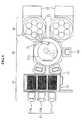
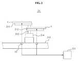
- FIG. 1is a plane view illustrating an entire system of an atomic layer deposition apparatus according to exemplary embodiments herein;
- FIG. 2is a front view illustrating a transfer robot according to exemplary embodiments herein;
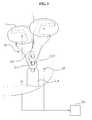
- FIG. 3is a perspective view illustrating a main part of the transfer robot of FIG. 2 ;
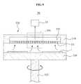
- FIG. 4is a cross-sectional view illustrating the atomic layer deposition apparatus of FIG. 1 ;
- FIG. 5is a perspective view of a main part of a process module of the atomic layer deposition apparatus of FIG. 4 ;
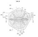
- FIG. 6is a plane view illustrating a gas spraying unit in the process module of FIG. 5 ;
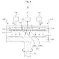
- FIG. 7is a cross-sectional view taken along line I-I in the gas spraying unit of FIG. 6 ;
- FIG. 8is a plane view illustrating the gas spraying unit of FIG. 6 according to other exemplary embodiments herein;
- FIG. 9is a cross-sectional view taken along line II-II in the gas spraying unit of FIG. 8 ;
- FIG. 10is a cross-sectional view taken along line III-III in the gas spraying unit of FIG. 8 ;
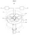
- FIG. 11is a perspective view of a main part for describing an operation in which a transfer robot loads a substrate on a susceptor unit in the atomic layer deposition apparatus of FIG. 1 ;
- FIG. 12is a perspective view illustrating a heater unit of the process module of FIG. 4 ;
- FIG. 13is a cross-sectional view illustrating the heater unit of FIG. 12 ;
- FIG. 14is a plane view for describing an example of a pattern of a heating device in the heater unit of FIG. 12 .
- FIG. 1is a plane view illustrating an entire system of an atomic layer deposition apparatus according to an exemplary embodiment.
- the atomic layer deposition apparatusincludes a loading/unloading module 10 for loading/unloading a substrate 1 on the atomic layer deposition apparatus, a process module 30 where a deposition process of an atomic layer is performed, and a transfer module 20 formed between the loading/unloading module 10 and the process module 30 , for transferring the substrate 1 .
- the substrate 1for example may be a silicon wafer. That is, the substrate 1 may be a transparent substrate including a glass used for a flat display apparatus such as a liquid crystal display (LCD) and a plasma display panel (PDP). Also, a shape and type of the substrate 1 may not be limited to embodiments as shown in the accompanying drawings and thus, the substrate 1 may practically have various shapes and sizes such as a circle, a rectangle, and the like.
- a shape and type of the substrate 1may not be limited to embodiments as shown in the accompanying drawings and thus, the substrate 1 may practically have various shapes and sizes such as a circle, a rectangle, and the like.
- the load port 11may be a device where the plurality of substrates are received and stored, and may be a cassette or a front opening unified pod (FOUP). Also, since the process module 10 simultaneously performs the deposition process with respect to the plurality of substrates 1 , the loading/unloading module 10 may include a plurality of load ports 11 a , 11 b , and 11 c.
- FOUPfront opening unified pod
- the load buffer unit 12may draw out the substrates 1 from the load port 11 , and transport the substrates 1 to the load-lock unit 13 .
- the load-lock unit 13may transport the substrates 1 to the load port 11 and the load port 11 may receive the substrates 1 .
- the load buffer unit 12may include a robot (not illustrated) for drawing out/receiving the substrates 1 from the load port 11 and the load-lock unit 13 and transporting the substrates 1 , and an aligner (not illustrated) for aligning the substrates 1 when drawing out/receiving the substrates 1 .
- a high-vacuum state of the transfer module 20 similar to that of the process module 30may be maintained to transport the substrates 1 to the process module 30 .
- the transfer module 20may be communicated with an atmosphere when the substrates 1 are loaded/unloaded in the loading/unloading unit 10 , and thereby a vacuum state of the transfer module 20 may be broken, and an internal environment of the transfer module 20 and the process module 30 may be rapidly changed.
- the interior of the transfer module 20 and the process module 30may be required to be in the high-vacuum state in order to perform the deposition process of the atomic layer after loading/unloading the substrates 1 , so that the deposition process may be delayed, causing occurrence of defectives.
- the load-lock unit 13may be formed to be selectively communicated with the loading/unloading module 10 and the transfer module 20 or to be sealed/blocked, and also to decompress/pressurize an internal pressure of the load-lock unit 13 to match with the loading/unloading module 10 and the transfer module 20 , so that the load-lock unit 13 may transport the substrates 1 between the loading/unloading module 10 and the transfer module 20 , while preventing a vacuum state of the transfer module 20 from being broken.
- a space communicated with the atmosphere when loading/unloading the substrates 1may be restricted by the load-lock unit 13 , and thereby may prevent occurrence of a time delay at the time of the decompressing/pressurizing.
- the transfer module 20may include a transfer module 21 for simultaneously transporting the plurality of substrates. A detailed technical configuration of the transfer robot 21 will be described later with reference to FIGS. 2 to 3 .
- the process module 30may include a process chamber 31 where the substrates 1 are received to perform the deposition process, and a deposition gas providing unit 33 for providing a deposition gas to the process chamber 31 .
- the process module 30may include two process chambers 31 where six pieces of substrates 1 are received, respectively, so that the deposition process may be simultaneously performed with respect to 12 pieces of the substrates 1 .
- embodiments described hereinare not limited thereto and thus, a number of substrates 1 enabled to be simultaneously processed in the process module 30 and a type of the process module 30 may be practically changed in a variety manner.
- a buffer 14may be provided in a side of the transfer module 20 .
- the buffer 14may enable the number of substrates 1 of the load port 11 and a number of substrates 1 of the process chamber 31 to be in multiples of each other when loading/unloading the substrates 1 , thereby preventing some substrates 1 from remaining or be lacking in the load port 11 .
- the buffer 14may be a device where the plurality of substrates 1 are received and stored, similar to the load port 11 , and may be provided in the side of the transfer module 20 , so that the transfer robot 21 draws out the substrates 1 from the buffer 14 . Also, the buffer 14 may selectively decompress/pressurize an internal pressure of the buffer 14 , similar to the load-lock unit 13 , and thereby may prevent a vacuum state of the transfer module 20 from being broken when transporting the substrates 1 . Also, the buffer 14 may selectively seal a connection portion with the transfer module 20 .
- the process module 30may simultaneously receive 12 pieces of substrates 1
- the load port 11may include three load ports 11 a , 11 b , and 11 c where 25 pieces of substrates 1 are respectively stored.
- the transfer robot 21may simultaneously transport two pieces of substrates 1 to load the substrates 1 on two process chambers 31 , respectively.
- the load buffer unit 12may draw out two substrates 1 from each of first to third ports 11 a , 11 b , and 11 c , and the load-lock unit 13 may load, one by one, the substrates drawn out from the load buffer unit 12 , on the transfer robot 21 .
- the loading/unloading module 10may include two load-lock units 13 to thereby load a single piece of the substrates 1 on each of two handling arms 211 and 212 of the transfer robot 21 , and the transfer robot 21 may simultaneously load two pieces of the substrates 1 on each of two process chambers 31 in a sequential manner.
- the substrates 1when the substrates 1 are drawn out from the load port 11 , two pieces of the substrates 1 are drawn out from each of the load ports 11 a , 11 b , and 11 c twelve times and thus, a single piece of the substrate 1 may remain in each of the load ports.
- the remaining substrates 1may be replenished in the process chamber 31 by drawing out the substrates 1 received in the buffer 14 .
- the buffer 14may function to prevent generation of extra substrates 1 in the load port 11 occurring when the number of substrates 1 received in the process module 30 and the number of substrates 1 stored in the loading/unloading module 10 are not in multiples of each other, and also prevent a delay of the process occurring when supplementing the substrates 1 to thereby improve a throughput.
- FIGS. 2 and 3are used for describing a detection operation concerning whether the substrate 1 is securely seated in the transfer module 20 of the atomic deposition apparatus of FIG. 1 .
- FIG. 2is a front view illustrating the transfer robot 21 according to exemplary embodiments
- FIG. 3is a perspective view illustrating a main part of the transfer robot 21 of FIG. 2 .
- the transfer robot 21 enabling simultaneous transport of two pieces of the substrates 1will be exemplarily described.
- the transfer robot 21 enabling simultaneous transporting of at least two pieces of substrates 1may be practically adopted, the embodiments herein are not limited thereto.
- the transfer robot 21may include handling arms 211 and 212 for simultaneously transporting two pieces of substrates 1 , driving arms 213 and 214 for driving the handling arms 211 and 212 to be moved linearly, rotatively, and vertically, and a driving portion 215 .
- the handling arms 211 and 212may hold the substrates 1 from a lower portion of the substrates 1 , and transport the substrates 1 .
- the handling arms 211 and 212may have a length corresponding to a diameter of the substrates 1 and a predetermined width and size, and thereby may securely hold the substrates.
- the handling arms 211 and 212may be formed into a shape by which interference with a lift pin 321 are not generated when loading/unloading the substrates 1 , while securely supporting the lower portion of the substrates 1 .
- the handling arms 211 and 212may be formed into a loop-shape such as ‘C-shape’ or ‘ -shape’.
- the respective shapes of the transfer robot 21 and the handling arms 211 and 212are not restricted as illustrated in the accompanying drawings and thus, various shapes of the handling arms 211 and 212 enabling to contact and support the lower portion and edges of the substrates 1 may be practically given.
- the driving arms 213 and 214 and the driving portion 215may be connected with the handling arms 211 and 212 to enable the handling arms 211 and 212 to be moved linearly, rotatively, and vertically, and may supply and transmit a driving power required for driving the handling arms 211 and 212 .
- the handling arms 211 and 212enabling to simultaneously transport two pieces of the substrates 1
- a size of each of the transfer module 20 and the transfer robot 21may increase, and a size of a space required for operations of the transfer robot 21 may also increase.
- the handling arms 211 and 212may be formed to be vertically spaced apart from each other by a predetermined interval.
- the handling arms 211 and 212are moved in parallel in a state of being vertically overlapped, and when loading/unloading the substrates 1 , the handling arms 211 and 212 are laterally rotated by a predetermined angle, to be expanded in a ‘V-shape’ as illustrated in FIG. 3 .
- the transfer module 20may include a sensor 22 for checking whether two pieces of the substrates 1 are securely seated on the transfer robot 21 .
- the handling arms 211 and 212may be required to be laterally rotated by a predetermined angle at the time of the checking of the sensor 22 , so that the two pieces of the substrates are partially overlapped.
- the sensor 22may include two optical sensors where a light is irradiated towards the substrates 1 seated on the handling arms 211 and 212 from a location where the substrates 1 are not overlapped and an interference does not occur by the handling arms 211 and 212 .
- a sensor controlling portion 221may generate a failure signal to stop the process, in a case where any one of the two pieces of the substrates 1 are not securely seated on the handling arms 211 and 212 .
- FIG. 4is a cross-sectional view illustrating a part of the process module 30 and the transfer module 20 in the atomic layer deposition apparatus of FIG. 1
- FIG. 5is a perspective view of a main part of the process module 30 of the atomic layer deposition apparatus of FIG. 4 .
- the process module 30includes two process chambers 31 where six pieces of the substrates 1 are received to perform the deposition process.
- the process chamber 31includes a susceptor unit 320 on which the substrate 1 is seated, a gas spraying unit 310 for providing a deposition gas to the substrates 1 , and a heater unit 330 for heating the substrates 1 and the susceptor unit 320 for the purpose of the deposition process.
- a detailed technical configuration of the process module 30is not an aspect of the present invention. Thus, descriptions and drawings describing technical configurations of respective components of the process module 30 will be omitted.
- a doorway 301 where the transfer robot 21 is moved outward or inward when loading/unloading the substrates 1 , and a door 302 for opening/closing the doorway 301are illustrated in FIG. 4 . That is, the doorway 301 may be opened by the door 302 when loading/unloading the substrates 1 , as illustrated in FIG. 4 , to thereby allow the transfer robot 21 to be moved inward or outward, and the doorway 31 may be closed by the door 302 while performing the deposition process, thereby sealing the process chamber 31 .
- the gas spraying unit 310may be provided on an upper portion of the process chamber 31 , and provide the deposition gas to the substrates 1 supported by the susceptor unit 320 .
- a method of depositing the atomic layermay be performed such that different deposition gases including a source material used for forming a thin film are reacted on a surface of the substrates 1 to form a thin film having a predetermined thickness.
- the gas spraying unit 310may be fixed, and the susceptor unit 320 may be rotatably provided in parallel with the gas spraying unit 310 .
- the gas spraying unit 310may include a plurality of spraying regions 400 (see FIG. 6 ) by which the deposition gases are sequentially sprayed on the substrates 1 while the susceptor unit 320 is rotated, and an exhaust portion 350 for drawing in an exhaust gas from inside the process chamber 31 and exhausting the drawn in gas above the process chamber 31 .
- the deposition gases of the present inventionmay designate gases used in a process of depositing the thin film, and include at least one source gas including a source material constituting the thin film intended to be deposited on the substrates 1 , and at least one purge gas for purging the source gas from the substrates 1 .
- the present exemplary embodimenttwo source gases that are mutually chemically reacted to form the thin film and one purge gas for purging the source gas may be used.
- first source gas (S 1 ) for depositing a silicon thin filmone of silane (SiH 4 ) or disilane (Si 2 H 6 ) each including silicon, SiF 4 and a metal organic chemical compound, and as a second source gas (S 2 ), a reactive gas decomposed by O 2 or O 3 and plasma may be used.
- the purge gas (PG)a stable gas that is not chemically reacted with the first and second source gases S 1 and S 2 and the thin film deposited on the substrates 1 may be used, and for example, gases such as argon (Ar), nitrogen (N 2 ), helium (He) may be used alone or in a mixture of two or more.
- gasessuch as argon (Ar), nitrogen (N 2 ), helium (He) may be used alone or in a mixture of two or more.
- the embodiments hereinare not limited thereto and thus, a number and type of the deposition gases may be practically and diversely changed.
- the gas spraying unit 310will be described in detail with reference to FIGS. 6 to 10 .
- FIG. 6is a plane view illustrating the gas spraying unit 310 in the process module 30 of FIG. 5
- FIG. 7is a cross-sectional view taken along line I-I in the gas spraying unit 310 of FIG. 6
- FIG. 8is a plane view illustrating the gas spraying unit of FIG. 6 according to other exemplary embodiments herein
- FIG. 9is a cross-sectional view taken along line II-II in the gas spraying unit 310 of FIG. 8
- FIG. 10is a cross-sectional view taken along line in the gas spraying unit 310 of FIG. 8 .
- each of the plurality of spraying regions 400 of the gas spraying unit 310may be formed into a fan-shape, and the plurality of spraying region 400 may be divided into a first source region 410 where a first source gas is sprayed, a first purge region 430 where a purge gas is sprayed, a second source region 420 where a second source gas is sprayed, and a second purge region 440 where the purge gas is sprayed, along a movement direction of the substrates 1 .
- four different types of gasesare respectively sprayed via the plurality of spraying regions 400 .
- the gas spraying unit 310may include a plurality of spraying holes 311 where the deposition gases are sprayed, and a spraying buffer 312 , that is, a flow path by which the deposition gases are supplied to the plurality of spraying holes 311 .
- a deposition gas supplying unit 33may be provided in a side of the spraying buffer 312 and adopted for supplying the deposition gas to the spraying buffer 312 .
- the deposition gas supplying unit 33includes a first supplying portion 33 a for supplying the first source gas (S 1 ), a second supplying portion 33 b for supplying the second source gas (S 2 ), and a third supplying portion 3 c for supplying the PG.
- the plurality of spraying holes 311may be formed in a predetermined pattern. Also, the plurality of spraying holes 311 may be formed such that a trace of the sprayed deposition gas is linearly brought into contact with the substrates 1 when the substrates 1 are moved by rotation of the susceptor unit 320 to cover the entire surface of the substrates 1 .
- the plurality of spraying holes 311may be arranged in a linear type that is approximately perpendicular to the movement direction of the substrates 1 , so that the substrates 1 and the deposition gas sprayed from the plurality of spraying holes 311 may be crossed with each other in the linear type, thereby uniformly maintaining a period during which the deposition gas is in contact with the surface of the substrates 1 .
- embodiments as illustrated in the accompanying drawingsare non-limiting and thus, a size and an arranged type of the plurality of spraying holes 311 may be practically and diversely changed.
- the gas spraying unit 310may include the plurality of spraying regions 400 , defined as the plurality of spraying holes 311 via which the deposition gases are sprayed to the substrates 1 , in accordance with a number of deposition gases.
- the plurality of spraying regions 400may be divided into the first and second source regions 410 and 420 via which the first and second source gases S 1 and S 2 are sprayed, respectively, and two purge regions 430 and 440 via which the PG is sprayed.
- the two purge regions 430 and 440may be provided between the first and second source regions 410 and 420 , respectively.
- the plurality of spraying regions 400may be formed into a fan-shape that may divide the gas spraying unit 301 into approximately four parts.
- the gas spraying unit 310may be connected with an exhaust unit 35 for drawing in/exhausting an exhaust gas inside the process chamber 31 , and include an exhaust portion 350 for drawing in the exhaust gas from above the substrates 1 in the process chamber 31 and exhausting the exhaust gas to the outside.
- the exhaust portion 350includes a plurality of exhaust lines 511 and 512 having a plurality of exhaust holes 351 for drawing in the exhaust gas inside the process chamber 31 , and an exhaust buffer 352 , that is, a flow path of the exhaust gas drawn in from the plurality of exhaust holes 351 .
- the plurality of exhaust lines 511 and 512may be defined as the plurality of exhaust holes 351 formed along a boundary of the plurality of spraying regions 400 , and may function to divide the plurality of spraying regions 400 as well as to draw in the exhaust gas via the plurality of exhaust holes 351 and to exhaust the exhaust gas.
- the exhaust portion 350may be formed along the boundary of each of the plurality of spraying regions 400 , so that two exhaust lines 511 and 512 are formed in a ‘U-shape’ or a ‘ -shape’ to divide the gas spraying unit 310 into approximately four regions.
- the exhaust portion 350may include two exhaust lines 511 and 512 formed into a ‘V-shape’, which are linear-symmetrical to each other.
- the two exhaust lines 511 and 512may serve as a physical barrier for preventing the source gases from being mixed between the source regions 410 and 420 while ensuring a maximal area of the source regions 410 and 420 .
- vertexes of the ‘V-shape’ facing each othermay be located in a center portion of the gas spraying unit 310 .
- a size, a number, and an arranged type of the plurality of spraying holes 311are not limited to embodiments as illustrated in the accompanying drawings and thus, the plurality of spraying holes 311 may be practically and diversely arranged to uniformly spray the deposition gases to the substrates 1 . Also, the plurality of spraying holes 311 may be formed into a circular-shape or a slit-shape. Similarly, a size, a number, and an arranged type of the plurality of exhaust holes 351 are not limited to embodiments as illustrated in the accompanying drawings and thus, the plurality of exhaust holes 351 may be practically and diversely arranged.
- the exhaust portion 350may include the plurality of exhaust lines 511 and 512 for preventing the source gases S 1 and S 2 from being mixed between the first and second source regions 410 and 420 , which are adjacent to each other in the center portion of the gas spraying unit 310 , in characteristics in the form of plurality of spraying regions 400 .
- the exhaust portion 350may include a center exhaust block 515 or 516 formed such that the exhaust lines 511 and 512 are adjacent to each other in the center portion of the gas spraying unit 310 , and the center exhaust block 515 or 516 is illustrated as a dotted line box in FIGS. 6 and 8 .
- the center exhaust block 515may be defined as a portion of the exhaust lines 511 and 512 formed in the center portion of the gas spraying unit 310 , and may be connected with the exhaust lines 511 and 512 .
- the center exhaust block 515may have the exhaust buffer 352 formed separately from the exhaust lines 511 and 512 .
- being connectively formed between the exhaust lines 511 and 512 with the center exhaust block 515may designate being communicatively formed between a buffer where an exhaust gas drawn in via the exhaust lines 511 and 512 is exhausted and a buffer where an exhaust gas drawn in via the center exhaust block 515 is exhausted.
- the exhaust lines 511 and 512 and the center exhaust blockmay be connectively formed.
- the exhaust gasincludes a non-reacted source material
- the exhaust gases drawn in from the first and second source regions 410 and 420 , respectivelyare mixed and reacted inside the exhaust buffer 352 to thereby generate particles.
- the first and second source regions 410 and 420may need to be formed to exhaust the exhaust gases via the exhaust lines 511 and 512 , each having a separate flow path.
- the purge regions 430 and 440may exhaust the exhaust gases using the same exhaust lines 511 and 512 as those in the first source region 410 or the second source region 420 .
- the first exhaust line 511 for drawing in exhaust gases from the first source region 410 and the purge regions 430 and 440 , and the second exhaust line 512 for drawing in exhaust gases from the second source region 420 and the purge regions 430 and 440may be provided.
- the exhaust buffers 352 a and 352 bmay be partitioned inside the center exhaust block 516 , so that the exhaust gases drawn in from the first source region 410 and the second source region 420 , respectively, are not mixed.
- the first source region 410 and the second source region 420may be adjacent to each other in the center portion of the gas spraying unit 310 .
- the center exhaust block 515is formed in the center portion of the gas spraying unit 310 , so that a physical barrier between the first and second source regions 410 and 420 is formed by means of the center exhaust block 515 in the center portion of the gas spraying unit 310 to thereby prevent inflow and mixing of the first and second source gases S 1 and S 2 .
- the center portion (CA) of the susceptor unit 320may be defined as a region where a vortex of gases is generated while the exhaust gases flow in, and may approximately designate a region where the substrates 1 are not seated on the susceptor unit 320 .
- the center exhaust block 515may increase an exhaust quantity of the exhaust gas from the center portion (CA) of the susceptor unit 320 where the vortex and stagnancy phenomenon of the exhaust gas are generated, thereby preventing the vortex and stagnancy phenomenon of the exhaust gas from being generated.
- the plurality of exhaust holes 351are formed in the center portion of the gas spraying unit 310 corresponding to the center portion (CA) of the susceptor unit 320 , thereby increasing the exhaust quantity of the exhaust gas from the center portion (CA) of the susceptor unit 320 .
- the two exhaust lines 511 and 512 formed along the boundary of the plurality of spraying regions 400may be adjacent to each other in the center portion of the gas spraying unit 310 , and the center exhaust block 515 may be formed such that the plurality of exhaust holes 351 are disposed over an entire region corresponding to the center portion (CA) of the susceptor unit 320 .
- the center exhaust block 515may be formed in the center portion of the gas spraying unit 310 , as illustrated in FIG. 6 and FIG. 8 , in a linear type having a predetermined length. Also, the center exhaust block 515 may have a more expanded type than the exhaust lines 511 and 512 to correspond to a size of the center portion (CA) of the susceptor unit 320 .
- an area of the exhaust lines 511 and 512 and a number of the plurality of exhaust holes 351may need to increase.
- the gas spraying unit 310 including the exhaust lines 511 and 512 of which an area increasesis exemplarily illustrated.
- the other exemplary embodimentswhich will be described in detail below, may be practically the same as the above described exemplary embodiments, except for a type of the exhaust lines 511 and 512 .
- like reference numeralsmay refer to the like elements throughout, and repeated descriptions will be omitted.
- the exhaust portion 350may include the exhaust lines 511 and 512 formed along the boundary of the plurality of spraying regions 400 , and the center exhaust block 516 formed in the center portion of the gas spraying unit 310 and adopted for drawing in/exhausting an exhaust gas in the center portion (CA) of the susceptor unit 320 .
- the exhaust portion 350may include two exhaust lines 511 and 512 formed into a ‘U-shape’ or ‘ -shape’ while the two exhaust lines 511 and 512 roughly divide the gas spraying unit 310 into four regions, and two auxiliary exhaust blocks 513 and 514 may also include traversing the gas spraying unit 310 along a diameter direction of the gas spraying unit 310 .
- the two exhaust lines 511 and 512are formed to thereby prevent exhaust gases drawn in from the first and second source regions 410 and 420 from being mixed, and the two auxiliary exhaust blocks 513 and 514 may be formed traversing the purge regions 430 and 440 .
- the first and second gases S 1 and S 2may be heavy in one direction, and thereby a thickness of a film deposited on the substrates 1 may be non-uniformly generated.
- the auxiliary exhaust blocks 513 and 514may be formed in the purge regions 430 and 440 , thereby adjusting the sprayed pressure of the purge gas (PG).
- regions 431 , 432 , 441 , and 442 not described in FIG. 8designate regions where the purge regions 430 and 440 are respectively partitioned by the auxiliary exhaust blocks 513 and 514 .
- the exhaust lines 511 and 512may be connected with the auxiliary exhaust blocks 513 and 514 , or may be formed separately from each other. However, the exhaust lines 511 and 512 and the auxiliary exhaust blocks 513 and 514 may be formed to prevent the exhaust gases drawn in from the first and second source regions 410 and 420 from being mixed.
- the gas spraying unit 310may include the plurality of exhaust holes 351 which is densely arranged in the center portion of the gas spraying unit 310 , and the center exhaust block 516 for drawing in the exhaust gas from the center portion (CA) of the susceptor unit 320 .
- the center exhaust block 516may be formed communicatively with or separately from the exhaust lines 511 and 512 and the auxiliary exhaust blocks 513 and 514 . However, at least two center exhaust block 516 may be formed to prevent the exhaust gases drawn in from the first and second source regions 410 and 420 from being mixed, and the two center exhaust blocks 516 may include exhaust buffers 352 a and 352 b , each having a separate flow path.
- the susceptor unit 320 and the heater unit 330will be described in detail with reference to FIGS. 11 to 14 .
- FIG. 11is a perspective view of a main part for describing an operation in which the transfer robot 21 loads substrates on the susceptor unit 320 in the atomic layer deposition apparatus of FIG. 1
- FIG. 12is a perspective view illustrating the heater unit 330 of the process module 30 of FIG. 4
- FIG. 13is a cross-sectional view illustrating the heater unit 330 of FIG. 12
- FIG. 14is a plane view for describing an example of a pattern of a heating device 333 in the heater unit 330 of FIG. 12 .
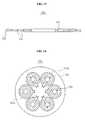
- the susceptor unit 320may be a semi-batch type having an excellent throughput, and the plurality of substrates 1 may be radially disposed along a circumferential direction of the susceptor unit 320 while being horizontally seated on an upper surface of the susceptor unit 320 .
- the susceptor unit 320may include a driving shaft 325 formed in a lower portion of the susceptor unit 320 .
- the driving shaft 325may be adopted for enabling the susceptor unit 320 to be rotated and also enabling vertical movement of the susceptor unit 320 when loading/unloading the substrates 1 .
- the susceptor unit 320may include a plurality of lift pins 321 on which the substrates are seated.
- a single piece of the substrate 1may be supported by three lift pins 321 , that is, by triangular three points, and three lift pins 321 may be provided in every location where the substrates 1 are seated.
- the substrates 1may not be seated on the upper surface of the susceptor unit 320 , and may be seated on the plurality of lift pins 321 , protruded from the upper surface of the susceptor unit 320 by a predetermined height, when loading the substrates 1 , as illustrated in FIG. 11 . Next, the substrates 1 may be seated on the upper surface of the susceptor unit 320 when the plurality of lift pins 321 descends.
- the plurality of lift pins 321may be formed passing through the susceptor unit 320 and may be vertically moved by vertical movement of the susceptor unit 320 .
- the susceptor unit 320may downwardly descend to a location where a lower surface of the susceptor unit 320 is relatively close to the heater unit 330 when loading/unloading the substrates 1 . Since the plurality of lift pins 321 pass through the susceptor unit 320 and are extended to a lower portion of the susceptor unit 320 by a predetermined length, a bottom of the lift pin 321 may be in close contact with an upper surface of the heater unit 330 when the susceptor unit 320 descends, and thereby and the lift pin 321 may be protruded above the susceptor unit 320 by a predetermined height due to restriction of movement of the lift pin 321 .
- the lift pin 321may be downwardly moved due to an unladen weight of the lift pin 321 and thus, the substrates 1 may be seated on the surface of the susceptor unit 320 .
- a part of an upper portion of the lift pin 321may be formed to have a diameter greater than that of a pin guide hole 331 of the heater unit 330 and thus, the upper portion of the lift pin 321 may be latched on the pin guide hole 331 .
- the substrate 1 having been already loadedmay be separated/erroneously dropped from its loaded/unloaded position due to the movement of the lift pin 321 and thus, the lift pin 321 may ascend only with respect to two substrates 1 corresponding to the loaded/unloaded position of the substrates 1 . That is, the vertical movement of the lift pin 321 may be carried out depending on whether the susceptor unit 320 is in close contact with the heater unit 330 when being vertically moved and thus, the heater unit 330 may include the pin guide hole 331 passing through the heater unit 330 to prevent the vertical movement of the lift pin 321 .
- a position corresponding to the two substrates 1 loaded/unloaded by the transfer robot 21 in the doorway 301may designate a loaded position 332 a
- a position corresponding to remaining four substrates 1may designate a seated position 332 b
- the pin guide hole 331 to allow the lift pin to the protruded therethroughmay not be formed in the loaded position 332 a of the heater unit 330 , however, the pin guide hole 331 may be formed in the remaining seated position 332 b , the lower portion of the lift pin 321 may be downwardly moved through the pin guide hole 331 when the susceptor unit 320 descends, and thereby the lift pin 321 may be prevented from being protruded.
- the transfer robot 21may load/unload two pieces of substrates 1 per each time, and six pieces of substrates 1 may be seated on the susceptor unit 320 and thus, the susceptor unit 320 may load/unload two pieces of substrates 1 per each time when being rotated at intervals of 120 degrees.
- the susceptor unit 320is rotated in a state where the lift pin 321 is received in the pin guide hole 331 of the heater unit 330 , the lift pin 321 , the susceptor unit 320 , and the heater unit 330 may be damaged.
- the susceptor unit 320is rotated in a state of ascending, the lift pin 321 of the loaded positions 332 a is protruded to enable the substrates 1 to be loaded/unloaded, and the lift pin 322 of the remaining seated positions 332 b is received in the pin guide hole 331 to maintain a seated state of the substrates 1 .
- the lift pin 321 of the loaded positions 332 amay be protruded in different heights to conform to the heights of the loaded substrates 1 .
- the transfer robot 21may simultaneously load two pieces of substrates 1 to the susceptor unit 320 , and the lift pin 321 may be disposed in a predetermined pattern to securely load/unload the substrates 1 .
- the handling arms 211 and 212may be disposed to be moved in a perpendicular manner to a base of a triangle formed by the lift pin 321 .
- the lift pin 321 provided on the two loaded locations 332 amay be disposed in a predetermined type.
- six lift pins 321 of the loaded locations 332 amay be provided in a regular triangle type or in an isosceles triangle type, and bases of two triangles formed by the six lift pins 321 may be formed to be disposed on a predetermined imaginary line (illustrated as a dashed dot line of FIG. 12 ).
- the heater unit 330may be mounted below the susceptor unit 320 , and may heat the susceptor unit 320 and the substrates 1 at a temperature required for the deposition process.
- the heater unit 330may include a heating element 333 for generating a heat when a power is applied, and the heating element 333 may be embedded in a housing 335 of the heater unit 330 .
- the heating element 333may be embedded in the housing 335 and thus, the heater unit 330 may be exposed to the deposition gas while the deposition process is carried out, and thereby may prevent a lifetime of the heater unit 330 from being reduced due to oxidization/damage of the heater unit 330 by the deposition gas, or prevent a temperature dispersion from being non-uniformly provided due to precipitation of impurities on the heater unit 330 .
- an interior of the housing 335may be maintained in a vacuum state or a high-vacuum state.
- the housing 335may be formed to block transmission of the heat to a lower portion of the heater unit 330 while effectively transmitting the heat emitted from the heating element 333 .
- the housing 335may be made of a chemically stable material while not causing a deformation of the housing 335 due to the heat generated in the heating element 333 .
- the housing 335may be made of a silicon nitride ceramic, a carbide ceramic, or a graphite material.
- a shielding membermay be provided in a lower portion of the housing 335 , that is, a portion of the housing 335 facing a lower portion of the heater unit 330 , to shield the heat generated in the heating element 333 from being transmitted to the lower portion of the heater unit 330 .
- the shielding membermay be provided in the lower portion of the housing 335 , or the lower portion of the housing 335 may be made of a material enabling heat shielding, and thereby prevent structures provided in the lower portion of the heater unit 330 from being thermally deformed by the heat generated in the heating element 333 , and the heat may be emitted only to the susceptor unit 320 to improve heat transfer efficiency of the heater unit 330 .
- the heating element 333may be a predetermined resistant heating element of heating a heat when a power is applied, and may have a wire type to be disposed in a predetermined type, thereby uniformly heating the substrates 1 inside the housing 335 .
- the element 333may include a filament, a coil, or a carbon wire.
- the heating element 333may be disposed in a curved line type so that a temperature of the substrates 1 may be uniformly heated and maintained. Also, the heating element 333 may be disposed over the heater unit 330 , however, may be provided in regions corresponding to each of the substrates 1 , as illustrated in 14 , to more accurately and uniformly heat the temperature of the substrates 1 , thereby forming a plurality of heating regions (for example, six heating regions).
- FIG. 14a pattern and a disposed type of the heating element 333 are illustrated.
- six heating elements 333may be separately provided in the regions corresponding to each of the substrates 1 to thereby form six heating regions.
- a temperature of each of the six regionsmay be uniformly heated to thereby uniformly maintain a temperature dispersion.
- the temperature of the heating element 333may be partially controlled.
- the heating element 333may have a wire type that enables the heating element 333 to be freely transformed, the heating element 333 may be formed into a shape that enables avoiding the structures and uniformly heating the substrates 1 , so that interferences with a structure inside the heater unit 330 and the pin guide hole 331 may be prevented from being generated.
- the heating element 333may include a terminal portion (not illustrated) used for connection with a power supplying portion (not illustrated), and the heating element 333 may be formed to minimize a number of the terminal portions.
- the heating element 333may have a predetermined curved-line type or an arbitrary adjustable curved-line type, and also have various shapes such as a spiral shape, a concentric circle, a linear shape, and the like.
Landscapes
- Engineering & Computer Science (AREA)
- Power Engineering (AREA)
- Physics & Mathematics (AREA)
- Condensed Matter Physics & Semiconductors (AREA)
- General Physics & Mathematics (AREA)
- Manufacturing & Machinery (AREA)
- Computer Hardware Design (AREA)
- Microelectronics & Electronic Packaging (AREA)
- Chemical & Material Sciences (AREA)
- General Chemical & Material Sciences (AREA)
- Chemical Kinetics & Catalysis (AREA)
- Robotics (AREA)
- Materials Engineering (AREA)
- Mechanical Engineering (AREA)
- Metallurgy (AREA)
- Organic Chemistry (AREA)
- Chemical Vapour Deposition (AREA)
- Container, Conveyance, Adherence, Positioning, Of Wafer (AREA)
Abstract
Description
- This application claims the benefit of Korean Patent Applications No. 10-2008-0135963, filed on Dec. 29, 2008, and No. 10-2009-0047519, filed on May 29, 2009 in the Korean Intellectual Property Office, the disclosures of which are incorporated herein by reference.
- 1. Field
- Exemplary embodiments relate to an atomic layer deposition apparatus, and more particularly, to an atomic layer deposition apparatus that may simultaneously load and unload a plurality of substrates to improve a throughput.
- 2. Description of the Related Art
- In general, to deposit a thin film with a predetermined thickness on a substrate such as a semiconductor substrate, a glass, and the like, there may be used a method of fabricating the thin film utilizing a physical vapor deposition (PVD) using physical collision such as sputtering, a chemical vapor deposition (CVD) using chemical reaction, and the like.
- As a design rule of a semiconductor device becomes rapidly minute, a thin film with a minute pattern is required, and a step, on which the thin film is formed, may become significantly great. Accordingly, an atomic layer deposition (ALD) that may significantly and uniformly form a minute pattern with an atomic layer thickness and have excellent step coverage has been increasingly used.
- In terms of using chemical reaction between gas molecules, the ALD may be similar to a general CVD. However, unlike the general CVD that may simultaneously inject a plurality of gas molecules into a process chamber, and deposit, on a substrate, a reaction product generated from an upper portion of the substrate, the ALD may inject a single gas element into the process chamber to purge the injected gas element, allow only a physically deposited gas to remain on a surface of a heated substrate, and inject other gas elements into the process chamber to thereby deposit a product of chemical reaction generated on the surface of the substrate. A thin film realized through the ALD may have an excellent step coverage property and a low impurity content and thus, is currently widely used.
- As for an existing ALD apparatus, there is disclosed an ALD of a semi-batch type in which a deposition process is simultaneously performed on a plurality of substrates to improve a throughput. In general, the ALD apparatus of the semi-batch type may be performed such that different deposition gases are injected and a substrate sequentially passes through an area where the deposition gases are injected by means of a high-speed rotation of a gas injection unit or susceptor unit, and a product of a chemical reaction between the deposition gases is deposited on the surface of the substrate to thereby form a thin film.
- Here, in the existing ALD apparatus, two process chambers of the semi-batch type are provided to perform a deposition process simultaneously with respect to 12 pieces of substrates. The ALD apparatus may include a transfer robot that may transport a substrate from a buffer to the process chamber, and load and unload the substrate on the process chamber. Here, an existing transfer robot may load/unload and transport the substrate one by one, and one transfer robot may be generally provided due to spatial limitations of the ALD apparatus.
- However, in the existing ALD apparatus, since one transfer robot serves to load/unload and transport the substrate, a time required for loading/unloading and transporting the 12 pieces of the substrate may be great. When a time is delayed in the transfer robot while loading/unloading and transporting the substrate, a time delay may occur during the deposition process to thereby reduce throughput and productivity. Also, in the buffer, 25 pieces or 50 pieces of substrates are generally stored, however a process module may perform the deposition process with respect to 12 pieces of the substrates, so that extra substrates may remain. As a result, a time required for replacing the buffer and supplementing the substrate may be needed due to treatment of the extra substrates.
- Exemplary embodiments provide an atomic layer deposition apparatus that may prevent a time delay occurring when loading/unloading and transporting a substrate.
- Exemplary embodiments also provide an atomic layer deposition apparatus that may improve a throughput and productivity of a deposition process.
- According to some exemplary embodiments, there is provided an atomic layer deposition apparatus, which enables to load/unload a plurality of substrates when moving the plurality of substrates to a process module, the apparatus including: a loading/unloading module for loading/unloading a substrate; a process module including a plurality of process chambers for simultaneously receiving a plurality of substrates and performing a deposition process, each of the plurality of process chambers including a gas spraying unit having an exhaust portion by which an exhaust gas is drawn in from inside the process chamber and the drawn-in gas is exhausted above the process chamber; and a transfer module including a transfer robot provided between the loading/unloading module and the process module, the transfer robot being adopted for simultaneously holding the plurality of substrates while transporting the substrate.
- The loading/unloading module may include a load port where the plurality of substrates are stored and a buffer, and, when loading the substrate, the buffer provides the same number of substrates as a number of substrates that are lacking so that a number of substrates stored in the load port and a number of substrates received in the process chamber are in multiples of each other. That is, the buffer may provide the same number of substrates as a number of substrates that are lacking in the load port when loading the substrate, thereby preventing extra substrates from being generated in the load port. For example, the buffer may be provided in a side of the transfer module, and an internal pressure of the buffer may be selectively decompressed/pressurized to prevent a vacuum state of the transfer module from being broken when transporting the substrate to the transfer module.
- Also, the transfer robot may include a plurality of handling arms, each for holding a single piece of the substrates, and the plurality of handling arms may be formed into a bar-shape or a ring-shape, each having a predetermined width and traversing a center portion of the substrate to correspond to a diameter of the substrate, so that the substrate is supported from a lower portion of the substrate. Here, the handling arms may prevent occurrence of interference between the handling arms with the lift pin or other structures when loading the substrate. Here, the plurality of handling arms of the transfer robot are vertically overlapped when transporting the substrates, and laterally expanded in a ‘V-shape’ when loading/unloading the substrates on the process chamber.
- Also, the transfer module may include a sensor for checking whether the substrate is securely seated on the transfer robot, and the sensor checks whether the substrate is securely seated on the transfer robot in a state where the handling arms are laterally expanded in the ‘V-shape’ to allow the substrates to be partially overlapped. For example, the sensor may be provided in a lower portion of the transfer module, and may include an optical sensor of checking whether the substrate is securely seated by irradiating a light to the substrate seated on the handling arms.
- Also, the process chamber may include a susceptor unit rotatably provided to allow the plurality of substrates to be laterally seated/supported and revolved, and being vertically movable in the process chamber; the gas spraying unit provided on an upper portion of the susceptor unit and including a plurality of spraying regions having at least one source region where a source gas is sprayed and at least one purge region where a purge gas is sprayed, the plurality of spraying regions being defined as a plurality of spraying hole groups by which a single gas of gases used to deposit a thin film on the substrate is provided; the exhaust portion provided on the gas spraying unit and adopted for drawing in the exhaust gas in the process chamber and exhausting the drawn-in gas; a heater unit provided on a lower portion of the susceptor unit and adopted for heating the substrate and the susceptor unit; and a lift pin provided on the susceptor unit to allow the substrate to be seated on the lift pin, and the lift pin being vertically movable to be protruded to the upper portion of the susceptor unit by means of a vertical movement of the susceptor unit.
- Here, the exhaust portion may include an exhaust line provided along a boundary of the plurality of spraying regions in the gas spraying unit, and defined as a plurality of exhaust hole groups by which the exhaust gas in the process chamber is drawn in and exhausted; and a center exhaust block formed in a center portion of the gas spraying unit and connected with the exhaust line, the center exhaust block being adopted for drawing in and exhausting an exhaust gas in a center portion of the susceptor unit.
- Also, the exhaust portion may include at least two exhaust lines formed to exhaust an exhaust gas drawn in from each of the at least one source region through different exhaust buffers of the at least two exhaust lines.
- Also, the exhaust line may be formed such that the exhaust gas drawn in from one of the at least one source region and an exhaust gas drawn in from one of the at least one purge region are exhausted through an identical single exhaust buffer.
- Also, the center exhaust block may include an exhaust path for exhausting an exhaust gas drawn in from the center exhaust block, and the exhaust path may be connected with or disconnected from an exhaust buffer.
- Also, the center exhaust block may have a region having a size corresponding to that of the center portion of the susceptor unit.
- Also, the center exhaust block may be formed such that an exhaust gas from each of the at least one source region is exhausted through different exhaust paths.
- Also, the exhaust line may further include an auxiliary exhaust block formed thereon to traverse the plurality of spraying regions, and the auxiliary exhaust block may include an exhaust path for exhausting an exhaust gas drawn in from the auxiliary exhaust block, the exhaust path being connected with the exhaust line and the center exhaust block, or being formed separately from the exhaust line and the center exhaust block.
- Also, the lift pin may be formed in such a manner as to pass through the susceptor unit and to be extended to the lower portion of the susceptor unit, and a lower end of the lift pin may be brought into contact with the heater unit when the susceptor unit descends, so that the lift pin is protruded to the upper portion of the susceptor unit, and the lift pin descends by its unladen weight when the susceptor unit ascends.
- Also, the heater unit may include a pin guide hole for receiving the lower end of the lift pin when the susceptor unit descends to prevent the lift pin from being protruded, and the pin guide hole may receive the lift pin of seated positions corresponding to remaining substrates excluding two pieces of loaded/unloaded substrates when the susceptor unit descends. That is, since the lift pin of the seated locations may not be protruded when loading/unloading the substrate, the substrate may be maintained in a state of being seated on the susceptor unit, and the lift pin of loaded positions may be protruded, and thereby the substrate may be seated on the lift pin.
- Also, since the handling arms may be formed to transport the substrate in a state where the handling arms are vertically overlapped, a difference in heights of the substrate seated on the handling arms when loading/unloading the substrate may be generated. Also, the lift pin of loaded positions corresponding to two pieces of loaded/unloaded substrates may be protruded in heights different from one another to correspond to a difference in heights where the substrate is loaded/unloaded.
- Also, the heater unit may include a heating element of a wire type or a filament type embedded in the heater unit for generating a heat when a power is applied in a sealed interior of a housing of the heater unit.
- Also, the heater unit may include a single or a plurality of heating elements of the heater unit disposed in a curved line-shape, so that a plurality of heating regions is created in locations corresponding to the plurality of substrates.
- Here, the housing of the heater unit may prevent a heat generated in the heating element from being emitted to a lower portion of the heater unit. Also, the housing of the heater unit may include a shielding member formed in a lower portion of the housing, for preventing the heat generated in the heating element from being emitted to the lower portion of the heater unit.
- As described above, according to exemplary embodiments, a transfer robot including a plurality of handling arms may be provided to simultaneously transport and load/unload at least two substrates, thereby effectively reducing a time required for transporting and loading/unloading the substrate, and preventing a time delay occurring in the transfer robot.
- Also, according to exemplary embodiments, a buffer may be provided to prevent some substrates from remaining on a load port when loading/unloading the substrates due to a number of substrates accommodated in the load port and a number of substrates simultaneously accommodated in a process chamber, and to prevent a process from being delayed due to treatment of extra substrates.
- These and/or other aspects will become apparent and more readily appreciated from the following description of exemplary embodiments, taken in conjunction with the accompanying drawings of which:
FIG. 1 is a plane view illustrating an entire system of an atomic layer deposition apparatus according to exemplary embodiments herein;FIG. 2 is a front view illustrating a transfer robot according to exemplary embodiments herein;FIG. 3 is a perspective view illustrating a main part of the transfer robot ofFIG. 2 ;FIG. 4 is a cross-sectional view illustrating the atomic layer deposition apparatus ofFIG. 1 ;FIG. 5 is a perspective view of a main part of a process module of the atomic layer deposition apparatus ofFIG. 4 ;FIG. 6 is a plane view illustrating a gas spraying unit in the process module ofFIG. 5 ;FIG. 7 is a cross-sectional view taken along line I-I in the gas spraying unit ofFIG. 6 ;FIG. 8 is a plane view illustrating the gas spraying unit ofFIG. 6 according to other exemplary embodiments herein;FIG. 9 is a cross-sectional view taken along line II-II in the gas spraying unit ofFIG. 8 ;FIG. 10 is a cross-sectional view taken along line III-III in the gas spraying unit ofFIG. 8 ;FIG. 11 is a perspective view of a main part for describing an operation in which a transfer robot loads a substrate on a susceptor unit in the atomic layer deposition apparatus ofFIG. 1 ;FIG. 12 is a perspective view illustrating a heater unit of the process module ofFIG. 4 ;FIG. 13 is a cross-sectional view illustrating the heater unit ofFIG. 12 ; andFIG. 14 is a plane view for describing an example of a pattern of a heating device in the heater unit ofFIG. 12 .- Reference will now be made in detail to exemplary embodiments, examples of which are illustrated in the accompanying drawings, wherein like reference numerals refer to the like elements throughout. Exemplary embodiments are described below to explain the present disclosure by referring to the figures.
- Hereinafter, an atomic layer deposition apparatus according to exemplary embodiments will be described in detail with reference to
FIGS. 1 to 14 . - An entire system of the atomic layer deposition apparatus will be described in detail with reference to
FIG. 1 .FIG. 1 is a plane view illustrating an entire system of an atomic layer deposition apparatus according to an exemplary embodiment. - Referring to
FIG. 1 , the atomic layer deposition apparatus includes a loading/unloading module 10 for loading/unloading asubstrate 1 on the atomic layer deposition apparatus, aprocess module 30 where a deposition process of an atomic layer is performed, and atransfer module 20 formed between the loading/unloading module 10 and theprocess module 30, for transferring thesubstrate 1. - Here, without limitation, the
substrate 1 for example may be a silicon wafer. That is, thesubstrate 1 may be a transparent substrate including a glass used for a flat display apparatus such as a liquid crystal display (LCD) and a plasma display panel (PDP). Also, a shape and type of thesubstrate 1 may not be limited to embodiments as shown in the accompanying drawings and thus, thesubstrate 1 may practically have various shapes and sizes such as a circle, a rectangle, and the like. - The loading/
unloading module 10 may include a component for loading/unloading thesubstrate 1 on the atomic layer deposition apparatus, and components for storing and receiving thesubstrate 1. For example, the loading/unloading module 10 may include a load port11 where a plurality ofsubstrates 1 are received and stored, aload buffer unit 12 for temporality receiving thesubstrates 1 before drawing out thesubstrates 1 from the load port11 and transporting thesubstrates 1 to thetransfer module 20, and a load-lock unit 13 provided between theload buffer unit 12 and thetransfer module 20 and adopted for decompressing/pressurizing an interior of the atomic layer deposition apparatus while preventing the interior of the atomic layer deposition apparatus from being rapidly changed due to inflow of outside air. - Here, detailed technical configurations of respective components of the loading/
unloading unit 10 are not central. Thus, descriptions and drawings describing technical configurations of respective components of the loading/unloading unit 10 are omitted. - For example, the load port11 may be a device where the plurality of substrates are received and stored, and may be a cassette or a front opening unified pod (FOUP). Also, since the
process module 10 simultaneously performs the deposition process with respect to the plurality ofsubstrates 1, the loading/unloading module 10 may include a plurality ofload ports 11a,11b, and11c. - The
load buffer unit 12 may draw out thesubstrates 1 from the load port11, and transport thesubstrates 1 to the load-lock unit 13. The load-lock unit 13 may transport thesubstrates 1 to the load port11 and the load port11 may receive thesubstrates 1. Here, theload buffer unit 12 may include a robot (not illustrated) for drawing out/receiving thesubstrates 1 from the load port11 and the load-lock unit 13 and transporting thesubstrates 1, and an aligner (not illustrated) for aligning thesubstrates 1 when drawing out/receiving thesubstrates 1. - In addition, since an interior of the
process module 30 is maintained in a state of a high-vacuum due to characteristics of the deposition process of the atomic layer, a high-vacuum state of thetransfer module 20 similar to that of theprocess module 30 may be maintained to transport thesubstrates 1 to theprocess module 30. Through a high-vacuum environment of thetransfer module 30, thetransfer module 20 may be communicated with an atmosphere when thesubstrates 1 are loaded/unloaded in the loading/unloading unit 10, and thereby a vacuum state of thetransfer module 20 may be broken, and an internal environment of thetransfer module 20 and theprocess module 30 may be rapidly changed. Also, the interior of thetransfer module 20 and theprocess module 30 may be required to be in the high-vacuum state in order to perform the deposition process of the atomic layer after loading/unloading thesubstrates 1, so that the deposition process may be delayed, causing occurrence of defectives. The load-lock unit 13 may be formed to be selectively communicated with the loading/unloading module 10 and thetransfer module 20 or to be sealed/blocked, and also to decompress/pressurize an internal pressure of the load-lock unit 13 to match with the loading/unloading module 10 and thetransfer module 20, so that the load-lock unit 13 may transport thesubstrates 1 between the loading/unloading module 10 and thetransfer module 20, while preventing a vacuum state of thetransfer module 20 from being broken. Also, a space communicated with the atmosphere when loading/unloading thesubstrates 1 may be restricted by the load-lock unit 13, and thereby may prevent occurrence of a time delay at the time of the decompressing/pressurizing. - The
transfer module 20 may include atransfer module 21 for simultaneously transporting the plurality of substrates. A detailed technical configuration of thetransfer robot 21 will be described later with reference toFIGS. 2 to 3 . - The
process module 30 may include aprocess chamber 31 where thesubstrates 1 are received to perform the deposition process, and a depositiongas providing unit 33 for providing a deposition gas to theprocess chamber 31. For example, theprocess module 30 may include twoprocess chambers 31 where six pieces ofsubstrates 1 are received, respectively, so that the deposition process may be simultaneously performed with respect to 12 pieces of thesubstrates 1. However, embodiments described herein are not limited thereto and thus, a number ofsubstrates 1 enabled to be simultaneously processed in theprocess module 30 and a type of theprocess module 30 may be practically changed in a variety manner. - In addition, when the number of
substrates 1 in which the deposition process is simultaneously performed in theprocess module 30 and a number ofsubstrates 1 provided in the load port11 are not in multiples of each other, somesubstrates 1 may remain or be lacking in the load port11. According to the present exemplary embodiment, abuffer 14 may be provided in a side of thetransfer module 20. In this instance, thebuffer 14 may enable the number ofsubstrates 1 of the load port11 and a number ofsubstrates 1 of theprocess chamber 31 to be in multiples of each other when loading/unloading thesubstrates 1, thereby preventing somesubstrates 1 from remaining or be lacking in the load port11. - The
buffer 14 may be a device where the plurality ofsubstrates 1 are received and stored, similar to the load port11, and may be provided in the side of thetransfer module 20, so that thetransfer robot 21 draws out thesubstrates 1 from thebuffer 14. Also, thebuffer 14 may selectively decompress/pressurize an internal pressure of thebuffer 14, similar to the load-lock unit 13, and thereby may prevent a vacuum state of thetransfer module 20 from being broken when transporting thesubstrates 1. Also, thebuffer 14 may selectively seal a connection portion with thetransfer module 20. - A method of loading the
substrates 1 in the atomic layer deposition apparatus will be herein described in detail. For example, as illustrated inFIG. 1 , theprocess module 30 may simultaneously receive 12 pieces ofsubstrates 1, and the load port11 may include threeload ports 11a,11b, and11cwhere 25 pieces ofsubstrates 1 are respectively stored. Thetransfer robot 21 may simultaneously transport two pieces ofsubstrates 1 to load thesubstrates 1 on twoprocess chambers 31, respectively. - In this case, the
load buffer unit 12 may draw out twosubstrates 1 from each of first tothird ports 11a,11b, and11c, and the load-lock unit 13 may load, one by one, the substrates drawn out from theload buffer unit 12, on thetransfer robot 21. Here, the loading/unloading module 10 may include two load-lock units 13 to thereby load a single piece of thesubstrates 1 on each of two handlingarms transfer robot 21, and thetransfer robot 21 may simultaneously load two pieces of thesubstrates 1 on each of twoprocess chambers 31 in a sequential manner. - In this manner, when the
substrates 1 are drawn out from the load port11, two pieces of thesubstrates 1 are drawn out from each of theload ports 11a,11b, and11ctwelve times and thus, a single piece of thesubstrate 1 may remain in each of the load ports. The remainingsubstrates 1 may be replenished in theprocess chamber 31 by drawing out thesubstrates 1 received in thebuffer 14. - According to the present exemplary embodiment, the
buffer 14 may function to prevent generation ofextra substrates 1 in the load port11 occurring when the number ofsubstrates 1 received in theprocess module 30 and the number ofsubstrates 1 stored in the loading/unloading module 10 are not in multiples of each other, and also prevent a delay of the process occurring when supplementing thesubstrates 1 to thereby improve a throughput. - However, embodiments as illustrated in the accompanying drawings are non-limiting and thus, the number of
substrates 1 received in theprocess chamber 31, a number of the load ports11, a number of thebuffers 14, and a number ofsubstrates 1 received in thebuffer 14 may be practically changed in a variety of manners. - Hereinafter, the
transfer module 20 and thetransfer robot 21 will be described in detail with reference toFIGS. 2 and 3 . For reference,FIGS. 2 and 3 are used for describing a detection operation concerning whether thesubstrate 1 is securely seated in thetransfer module 20 of the atomic deposition apparatus ofFIG. 1 . FIG. 2 is a front view illustrating thetransfer robot 21 according to exemplary embodiments, andFIG. 3 is a perspective view illustrating a main part of thetransfer robot 21 ofFIG. 2 .- Hereinafter, for convenience of descriptions, the
transfer robot 21 enabling simultaneous transport of two pieces of thesubstrates 1 will be exemplarily described. However, while thetransfer robot 21 enabling simultaneous transporting of at least two pieces ofsubstrates 1 may be practically adopted, the embodiments herein are not limited thereto. - Referring to
FIGS. 2 and 3 , thetransfer robot 21 may include handlingarms substrates 1, drivingarms arms portion 215. - The handling
arms substrates 1 from a lower portion of thesubstrates 1, and transport thesubstrates 1. In this instance, the handlingarms substrates 1 and a predetermined width and size, and thereby may securely hold the substrates. Also, the handlingarms lift pin 321 are not generated when loading/unloading thesubstrates 1, while securely supporting the lower portion of thesubstrates 1. For example, the handlingarms -shape’. However, the respective shapes of the
transfer robot 21 and the handlingarms arms substrates 1 may be practically given. - The driving
arms portion 215 may be connected with the handlingarms arms arms - In addition, as for the handling
arms substrates 1, as a size of thesubstrate 1 increases, a size of each of thetransfer module 20 and thetransfer robot 21 may increase, and a size of a space required for operations of thetransfer robot 21 may also increase. According to the present exemplary embodiment, to reduce the size of each of thetransfer robot 21 and thetransfer module 20, the handlingarms substrates 1, the handlingarms substrates 1, the handlingarms FIG. 3 . - Also, the
transfer module 20 may include asensor 22 for checking whether two pieces of thesubstrates 1 are securely seated on thetransfer robot 21. Here, since it is difficult to check whether the two pieces of thesubstrates 1 are securely seated on thetransfer robot 21 in a state where the handlingarms substrates 1, the handlingarms sensor 22, so that the two pieces of the substrates are partially overlapped. - For example, as illustrated in
FIGS. 2 and 3 , thesensor 22 may include two optical sensors where a light is irradiated towards thesubstrates 1 seated on the handlingarms substrates 1 are not overlapped and an interference does not occur by the handlingarms sensor 22, asensor controlling portion 221 may generate a failure signal to stop the process, in a case where any one of the two pieces of thesubstrates 1 are not securely seated on the handlingarms - However, embodiments as illustrated in the accompanying drawings are non-limiting and thus, a location and number of the
sensor 22 may be practically and diversely changed. Also, as thesensor 22, various means for checking whether thesubstrates 1 are securely seated on the handlingarms - Hereinafter, the
process module 30 will be described in detail with reference toFIGS. 4 to 14 . FIG. 4 is a cross-sectional view illustrating a part of theprocess module 30 and thetransfer module 20 in the atomic layer deposition apparatus ofFIG. 1 , andFIG. 5 is a perspective view of a main part of theprocess module 30 of the atomic layer deposition apparatus ofFIG. 4 .- The
process module 30 includes twoprocess chambers 31 where six pieces of thesubstrates 1 are received to perform the deposition process. Theprocess chamber 31 includes asusceptor unit 320 on which thesubstrate 1 is seated, agas spraying unit 310 for providing a deposition gas to thesubstrates 1, and aheater unit 330 for heating thesubstrates 1 and thesusceptor unit 320 for the purpose of the deposition process. Here, a detailed technical configuration of theprocess module 30 is not an aspect of the present invention. Thus, descriptions and drawings describing technical configurations of respective components of theprocess module 30 will be omitted. - In addition, a
doorway 301 where thetransfer robot 21 is moved outward or inward when loading/unloading thesubstrates 1, and adoor 302 for opening/closing thedoorway 301 are illustrated inFIG. 4 . That is, thedoorway 301 may be opened by thedoor 302 when loading/unloading thesubstrates 1, as illustrated inFIG. 4 , to thereby allow thetransfer robot 21 to be moved inward or outward, and thedoorway 31 may be closed by thedoor 302 while performing the deposition process, thereby sealing theprocess chamber 31. - The
gas spraying unit 310 may be provided on an upper portion of theprocess chamber 31, and provide the deposition gas to thesubstrates 1 supported by thesusceptor unit 320. - Here, a method of depositing the atomic layer may be performed such that different deposition gases including a source material used for forming a thin film are reacted on a surface of the
substrates 1 to form a thin film having a predetermined thickness. However, according to the present exemplary embodiment, thegas spraying unit 310 may be fixed, and thesusceptor unit 320 may be rotatably provided in parallel with thegas spraying unit 310. Thegas spraying unit 310 may include a plurality of spraying regions400 (seeFIG. 6 ) by which the deposition gases are sequentially sprayed on thesubstrates 1 while thesusceptor unit 320 is rotated, and anexhaust portion 350 for drawing in an exhaust gas from inside theprocess chamber 31 and exhausting the drawn in gas above theprocess chamber 31. - For reference, the deposition gases of the present invention may designate gases used in a process of depositing the thin film, and include at least one source gas including a source material constituting the thin film intended to be deposited on the
substrates 1, and at least one purge gas for purging the source gas from thesubstrates 1. According to the present exemplary embodiment, two source gases that are mutually chemically reacted to form the thin film and one purge gas for purging the source gas may be used. For example, as a first source gas (S1) for depositing a silicon thin film, one of silane (SiH4) or disilane (Si2H6) each including silicon, SiF4and a metal organic chemical compound, and as a second source gas (S2), a reactive gas decomposed by O2or O3and plasma may be used. As the purge gas (PG), a stable gas that is not chemically reacted with the first and second source gases S1 and S2 and the thin film deposited on thesubstrates 1 may be used, and for example, gases such as argon (Ar), nitrogen (N2), helium (He) may be used alone or in a mixture of two or more. However, the embodiments herein are not limited thereto and thus, a number and type of the deposition gases may be practically and diversely changed. - The
gas spraying unit 310 will be described in detail with reference toFIGS. 6 to 10 . FIG. 6 is a plane view illustrating thegas spraying unit 310 in theprocess module 30 ofFIG. 5 ,FIG. 7 is a cross-sectional view taken along line I-I in thegas spraying unit 310 ofFIG. 6 ,FIG. 8 is a plane view illustrating the gas spraying unit ofFIG. 6 according to other exemplary embodiments herein,FIG. 9 is a cross-sectional view taken along line II-II in thegas spraying unit 310 ofFIG. 8 , andFIG. 10 is a cross-sectional view taken along line in thegas spraying unit 310 ofFIG. 8 .- For example, as illustrated in
FIG. 6 , each of the plurality of sprayingregions 400 of thegas spraying unit 310 may be formed into a fan-shape, and the plurality of sprayingregion 400 may be divided into afirst source region 410 where a first source gas is sprayed, afirst purge region 430 where a purge gas is sprayed, asecond source region 420 where a second source gas is sprayed, and asecond purge region 440 where the purge gas is sprayed, along a movement direction of thesubstrates 1. In this instance, four different types of gases are respectively sprayed via the plurality of sprayingregions 400. - The
gas spraying unit 310 may include a plurality of sprayingholes 311 where the deposition gases are sprayed, and a sprayingbuffer 312, that is, a flow path by which the deposition gases are supplied to the plurality of sprayingholes 311. Also, a depositiongas supplying unit 33 may be provided in a side of the sprayingbuffer 312 and adopted for supplying the deposition gas to the sprayingbuffer 312. For example, the depositiongas supplying unit 33 includes a first supplyingportion 33afor supplying the first source gas (S1), a second supplyingportion 33bfor supplying the second source gas (S2), and a third supplying portion3cfor supplying the PG. - Here, so that the
gas spraying unit 310 uniformly provides the deposition gas to thesubstrates 1, the plurality of sprayingholes 311 may be formed in a predetermined pattern. Also, the plurality of sprayingholes 311 may be formed such that a trace of the sprayed deposition gas is linearly brought into contact with thesubstrates 1 when thesubstrates 1 are moved by rotation of thesusceptor unit 320 to cover the entire surface of thesubstrates 1. For example, the plurality of sprayingholes 311 may be arranged in a linear type that is approximately perpendicular to the movement direction of thesubstrates 1, so that thesubstrates 1 and the deposition gas sprayed from the plurality of sprayingholes 311 may be crossed with each other in the linear type, thereby uniformly maintaining a period during which the deposition gas is in contact with the surface of thesubstrates 1. However, embodiments as illustrated in the accompanying drawings are non-limiting and thus, a size and an arranged type of the plurality of sprayingholes 311 may be practically and diversely changed. - The
gas spraying unit 310 may include the plurality of sprayingregions 400, defined as the plurality of sprayingholes 311 via which the deposition gases are sprayed to thesubstrates 1, in accordance with a number of deposition gases. For example, the plurality of sprayingregions 400 may be divided into the first andsecond source regions purge regions purge regions second source regions FIG. 6 , the plurality of sprayingregions 400 may be formed into a fan-shape that may divide thegas spraying unit 301 into approximately four parts. - The
gas spraying unit 310 may be connected with anexhaust unit 35 for drawing in/exhausting an exhaust gas inside theprocess chamber 31, and include anexhaust portion 350 for drawing in the exhaust gas from above thesubstrates 1 in theprocess chamber 31 and exhausting the exhaust gas to the outside. Theexhaust portion 350 includes a plurality ofexhaust lines exhaust holes 351 for drawing in the exhaust gas inside theprocess chamber 31, and anexhaust buffer 352, that is, a flow path of the exhaust gas drawn in from the plurality of exhaust holes351. - Here, the plurality of
exhaust lines exhaust holes 351 formed along a boundary of the plurality of sprayingregions 400, and may function to divide the plurality of sprayingregions 400 as well as to draw in the exhaust gas via the plurality ofexhaust holes 351 and to exhaust the exhaust gas. For example, theexhaust portion 350 may be formed along the boundary of each of the plurality of sprayingregions 400, so that twoexhaust lines -shape’ to divide thegas spraying unit 310 into approximately four regions. Here, theexhaust portion 350 may include twoexhaust lines exhaust lines source regions source regions gas spraying unit 310. - In addition, a size, a number, and an arranged type of the plurality of spraying
holes 311 are not limited to embodiments as illustrated in the accompanying drawings and thus, the plurality of sprayingholes 311 may be practically and diversely arranged to uniformly spray the deposition gases to thesubstrates 1. Also, the plurality of sprayingholes 311 may be formed into a circular-shape or a slit-shape. Similarly, a size, a number, and an arranged type of the plurality ofexhaust holes 351 are not limited to embodiments as illustrated in the accompanying drawings and thus, the plurality ofexhaust holes 351 may be practically and diversely arranged. - In particular, the
exhaust portion 350 may include the plurality ofexhaust lines second source regions gas spraying unit 310, in characteristics in the form of plurality of sprayingregions 400. Hereinafter, theexhaust portion 350 may include acenter exhaust block exhaust lines gas spraying unit 310, and thecenter exhaust block FIGS. 6 and 8 . - Here, the
center exhaust block 515 may be defined as a portion of theexhaust lines gas spraying unit 310, and may be connected with theexhaust lines center exhaust block 515 may have theexhaust buffer 352 formed separately from theexhaust lines exhaust lines center exhaust block 515 may designate being communicatively formed between a buffer where an exhaust gas drawn in via theexhaust lines center exhaust block 515 is exhausted. In addition, as illustrated inFIG. 6 or8, theexhaust lines - In addition, since the exhaust gas includes a non-reacted source material, the exhaust gases drawn in from the first and
second source regions exhaust buffer 352 to thereby generate particles. Accordingly, the first andsecond source regions exhaust lines purge regions same exhaust lines first source region 410 or thesecond source region 420. According to the present exemplary embodiment, thefirst exhaust line 511 for drawing in exhaust gases from thefirst source region 410 and thepurge regions second exhaust line 512 for drawing in exhaust gases from thesecond source region 420 and thepurge regions FIG. 7 , as for thecenter exhaust block 515, the exhaust buffers352aand352bmay be partitioned inside thecenter exhaust block 516, so that the exhaust gases drawn in from thefirst source region 410 and thesecond source region 420, respectively, are not mixed. - Here, due to characteristics in the form of the plurality of spraying
regions 400 and thegas spraying unit 310, thefirst source region 410 and thesecond source region 420 may be adjacent to each other in the center portion of thegas spraying unit 310. However, according to the present exemplary embodiment, thecenter exhaust block 515 is formed in the center portion of thegas spraying unit 310, so that a physical barrier between the first andsecond source regions center exhaust block 515 in the center portion of thegas spraying unit 310 to thereby prevent inflow and mixing of the first and second source gases S1 and S2. - In addition, as illustrated in
FIG. 5 , in a process where an exhaust gas above thesuscepor unit 320 flows in towards a center portion (CA) of thesusceptor unit 320 when thesusceptor unit 320 is rotated in a high-speed, a vortex of the exhaust gases may be generated, causing a stagnancy phenomenon of the exhaust gases. Here, the center portion (CA) of thesusceptor unit 320 may be defined as a region where a vortex of gases is generated while the exhaust gases flow in, and may approximately designate a region where thesubstrates 1 are not seated on thesusceptor unit 320. - The
center exhaust block 515 may increase an exhaust quantity of the exhaust gas from the center portion (CA) of thesusceptor unit 320 where the vortex and stagnancy phenomenon of the exhaust gas are generated, thereby preventing the vortex and stagnancy phenomenon of the exhaust gas from being generated. - More specifically, as for the
center exhaust block 515, the plurality ofexhaust holes 351 are formed in the center portion of thegas spraying unit 310 corresponding to the center portion (CA) of thesusceptor unit 320, thereby increasing the exhaust quantity of the exhaust gas from the center portion (CA) of thesusceptor unit 320. Also, the twoexhaust lines regions 400 may be adjacent to each other in the center portion of thegas spraying unit 310, and thecenter exhaust block 515 may be formed such that the plurality ofexhaust holes 351 are disposed over an entire region corresponding to the center portion (CA) of thesusceptor unit 320. For example, thecenter exhaust block 515 may be formed in the center portion of thegas spraying unit 310, as illustrated inFIG. 6 andFIG. 8 , in a linear type having a predetermined length. Also, thecenter exhaust block 515 may have a more expanded type than theexhaust lines susceptor unit 320. - However, embodiments as illustrated in the accompanying drawings are non-limiting and thus, a type and location of the
exhaust lines center exhaust block 515 may be practically and diversely changed. - In addition, to increase the exhaust quantity in the
exhaust lines exhaust lines exhaust holes 351 may need to increase. - Referring to
FIGS. 8 to 10 , according to other exemplary embodiments of the present invention, thegas spraying unit 310 including theexhaust lines exhaust lines - As illustrated in
FIGS. 8 to 10 , theexhaust portion 350 may include theexhaust lines regions 400, and thecenter exhaust block 516 formed in the center portion of thegas spraying unit 310 and adopted for drawing in/exhausting an exhaust gas in the center portion (CA) of thesusceptor unit 320. - Also, the
exhaust portion 350 may include twoexhaust lines -shape’ while the twoexhaust lines gas spraying unit 310 into four regions, and two auxiliary exhaust blocks513 and514 may also include traversing thegas spraying unit 310 along a diameter direction of thegas spraying unit 310. The twoexhaust lines second source regions purge regions - Here, when a sprayed pressure of the PG is high, the first and second gases S1 and S2 may be heavy in one direction, and thereby a thickness of a film deposited on the
substrates 1 may be non-uniformly generated. The auxiliary exhaust blocks513 and514 may be formed in thepurge regions - In addition,
regions FIG. 8 designate regions where thepurge regions - The
exhaust lines exhaust lines second source regions - The
gas spraying unit 310 may include the plurality ofexhaust holes 351 which is densely arranged in the center portion of thegas spraying unit 310, and thecenter exhaust block 516 for drawing in the exhaust gas from the center portion (CA) of thesusceptor unit 320. Thecenter exhaust block 516 may be formed communicatively with or separately from theexhaust lines center exhaust block 516 may be formed to prevent the exhaust gases drawn in from the first andsecond source regions exhaust buffers - The
susceptor unit 320 and theheater unit 330 according to exemplary embodiments will be described in detail with reference toFIGS. 11 to 14 . FIG. 11 is a perspective view of a main part for describing an operation in which thetransfer robot 21 loads substrates on thesusceptor unit 320 in the atomic layer deposition apparatus ofFIG. 1 ,FIG. 12 is a perspective view illustrating theheater unit 330 of theprocess module 30 ofFIG. 4 ,FIG. 13 is a cross-sectional view illustrating theheater unit 330 ofFIG. 12 , andFIG. 14 is a plane view for describing an example of a pattern of aheating device 333 in theheater unit 330 ofFIG. 12 .- The
susceptor unit 320 may be a semi-batch type having an excellent throughput, and the plurality ofsubstrates 1 may be radially disposed along a circumferential direction of thesusceptor unit 320 while being horizontally seated on an upper surface of thesusceptor unit 320. For example, six pieces of thesubstrates 1 may be seated on the upper surface of thesusceptor unit 320 by predetermined intervals, and thesubstrates 1 may be resolved with respect to a center point of thesusceptor unit 320 when thesusceptor unit 320 is rotated. Thesusceptor unit 320 may include a drivingshaft 325 formed in a lower portion of thesusceptor unit 320. The drivingshaft 325 may be adopted for enabling thesusceptor unit 320 to be rotated and also enabling vertical movement of thesusceptor unit 320 when loading/unloading thesubstrates 1. - The
susceptor unit 320 may include a plurality of lift pins321 on which the substrates are seated. For example, a single piece of thesubstrate 1 may be supported by threelift pins 321, that is, by triangular three points, and threelift pins 321 may be provided in every location where thesubstrates 1 are seated. - The
substrates 1 may not be seated on the upper surface of thesusceptor unit 320, and may be seated on the plurality of lift pins321, protruded from the upper surface of thesusceptor unit 320 by a predetermined height, when loading thesubstrates 1, as illustrated inFIG. 11 . Next, thesubstrates 1 may be seated on the upper surface of thesusceptor unit 320 when the plurality of lift pins321 descends. - The plurality of lift pins321 may be formed passing through the
susceptor unit 320 and may be vertically moved by vertical movement of thesusceptor unit 320. - More specifically, as illustrated in
FIG. 4 , thesusceptor unit 320 may downwardly descend to a location where a lower surface of thesusceptor unit 320 is relatively close to theheater unit 330 when loading/unloading thesubstrates 1. Since the plurality of lift pins321 pass through thesusceptor unit 320 and are extended to a lower portion of thesusceptor unit 320 by a predetermined length, a bottom of thelift pin 321 may be in close contact with an upper surface of theheater unit 330 when thesusceptor unit 320 descends, and thereby and thelift pin 321 may be protruded above thesusceptor unit 320 by a predetermined height due to restriction of movement of thelift pin 321. Also, when thesusceptor unit 320 ascends for the deposition process, thelift pin 321 may be downwardly moved due to an unladen weight of thelift pin 321 and thus, thesubstrates 1 may be seated on the surface of thesusceptor unit 320. Here, to prevent thelift pin 321 from being erroneously dropped to the lower portion of thesusceptor unit 320, a part of an upper portion of thelift pin 321 may be formed to have a diameter greater than that of apin guide hole 331 of theheater unit 330 and thus, the upper portion of thelift pin 321 may be latched on thepin guide hole 331. - In addition, in a case where the plurality of lift pins321 are vertically moved when loading/unloading the
substrates 1 on thesusceptor unit 320, thesubstrate 1 having been already loaded may be separated/erroneously dropped from its loaded/unloaded position due to the movement of thelift pin 321 and thus, thelift pin 321 may ascend only with respect to twosubstrates 1 corresponding to the loaded/unloaded position of thesubstrates 1. That is, the vertical movement of thelift pin 321 may be carried out depending on whether thesusceptor unit 320 is in close contact with theheater unit 330 when being vertically moved and thus, theheater unit 330 may include thepin guide hole 331 passing through theheater unit 330 to prevent the vertical movement of thelift pin 321. - Here, for convenience of description, a position corresponding to the two
substrates 1 loaded/unloaded by thetransfer robot 21 in thedoorway 301 may designate aloaded position 332a, and a position corresponding to remaining foursubstrates 1 may designate aseated position 332b. As illustrated inFIG. 12 , thepin guide hole 331 to allow the lift pin to the protruded therethrough may not be formed in the loadedposition 332aof theheater unit 330, however, thepin guide hole 331 may be formed in the remaining seatedposition 332b, the lower portion of thelift pin 321 may be downwardly moved through thepin guide hole 331 when thesusceptor unit 320 descends, and thereby thelift pin 321 may be prevented from being protruded. - The
transfer robot 21 may load/unload two pieces ofsubstrates 1 per each time, and six pieces ofsubstrates 1 may be seated on thesusceptor unit 320 and thus, thesusceptor unit 320 may load/unload two pieces ofsubstrates 1 per each time when being rotated at intervals of 120 degrees. Here, when thesusceptor unit 320 is rotated in a state where thelift pin 321 is received in thepin guide hole 331 of theheater unit 330, thelift pin 321, thesusceptor unit 320, and theheater unit 330 may be damaged. Thus, so that thelift pin 321 is completely separated from thepin guide hole 331 when thesusceptor unit 330 is rotated, thesusceptor unit 320 is rotated in a state of ascending, thelift pin 321 of the loadedpositions 332ais protruded to enable thesubstrates 1 to be loaded/unloaded, and thelift pin 322 of the remaining seatedpositions 332bis received in thepin guide hole 331 to maintain a seated state of thesubstrates 1. - Also, since two pieces of the
substrates 1 are loaded/unloaded in different heights due to a difference of heights of the handlingarms transfer robot 21, thelift pin 321 of the loadedpositions 332amay be protruded in different heights to conform to the heights of the loadedsubstrates 1. - In addition, the
transfer robot 21 may simultaneously load two pieces ofsubstrates 1 to thesusceptor unit 320, and thelift pin 321 may be disposed in a predetermined pattern to securely load/unload thesubstrates 1. For example, the handlingarms lift pin 321. Also, to prevent thesubstrates 1 from colliding or interferences from being generated when the two pieces of the substrates are simultaneously loaded/unloaded, or when the handlingarms lift pin 321 provided on the two loadedlocations 332amay be disposed in a predetermined type. - For example, six
lift pins 321 of the loadedlocations 332amay be provided in a regular triangle type or in an isosceles triangle type, and bases of two triangles formed by the sixlift pins 321 may be formed to be disposed on a predetermined imaginary line (illustrated as a dashed dot line ofFIG. 12 ). - The
heater unit 330 may be mounted below thesusceptor unit 320, and may heat thesusceptor unit 320 and thesubstrates 1 at a temperature required for the deposition process. - The
heater unit 330 may include aheating element 333 for generating a heat when a power is applied, and theheating element 333 may be embedded in ahousing 335 of theheater unit 330. Theheating element 333 may be embedded in thehousing 335 and thus, theheater unit 330 may be exposed to the deposition gas while the deposition process is carried out, and thereby may prevent a lifetime of theheater unit 330 from being reduced due to oxidization/damage of theheater unit 330 by the deposition gas, or prevent a temperature dispersion from being non-uniformly provided due to precipitation of impurities on theheater unit 330. Here, to prevent inflow of the deposition gas to inside thehousing 335 from being blocked and to effectively transmit a heat generated by theheating element 333 to thesusceptor unit 320, an interior of thehousing 335 may be maintained in a vacuum state or a high-vacuum state. - The
housing 335 may be formed to block transmission of the heat to a lower portion of theheater unit 330 while effectively transmitting the heat emitted from theheating element 333. For example, thehousing 335 may be made of a chemically stable material while not causing a deformation of thehousing 335 due to the heat generated in theheating element 333. For example, thehousing 335 may be made of a silicon nitride ceramic, a carbide ceramic, or a graphite material. - Also, a shielding member (not illustrated) may be provided in a lower portion of the
housing 335, that is, a portion of thehousing 335 facing a lower portion of theheater unit 330, to shield the heat generated in theheating element 333 from being transmitted to the lower portion of theheater unit 330. Here, the shielding member may be provided in the lower portion of thehousing 335, or the lower portion of thehousing 335 may be made of a material enabling heat shielding, and thereby prevent structures provided in the lower portion of theheater unit 330 from being thermally deformed by the heat generated in theheating element 333, and the heat may be emitted only to thesusceptor unit 320 to improve heat transfer efficiency of theheater unit 330. - The
heating element 333 may be a predetermined resistant heating element of heating a heat when a power is applied, and may have a wire type to be disposed in a predetermined type, thereby uniformly heating thesubstrates 1 inside thehousing 335. - For example, the
element 333 may include a filament, a coil, or a carbon wire. - The
heating element 333 may be disposed in a curved line type so that a temperature of thesubstrates 1 may be uniformly heated and maintained. Also, theheating element 333 may be disposed over theheater unit 330, however, may be provided in regions corresponding to each of thesubstrates 1, as illustrated in14, to more accurately and uniformly heat the temperature of thesubstrates 1, thereby forming a plurality of heating regions (for example, six heating regions). - In
FIG. 14 , a pattern and a disposed type of theheating element 333 are illustrated. As illustrated inFIG. 14 , sixheating elements 333 may be separately provided in the regions corresponding to each of thesubstrates 1 to thereby form six heating regions. In this case, since the six regions are heated by each of theheating elements 333, a temperature of each of the six regions may be uniformly heated to thereby uniformly maintain a temperature dispersion. Also, by adjusting a power applied to each of theheating elements 333, the temperature of theheating element 333 may be partially controlled. - Here, since the
heating element 333 may have a wire type that enables theheating element 333 to be freely transformed, theheating element 333 may be formed into a shape that enables avoiding the structures and uniformly heating thesubstrates 1, so that interferences with a structure inside theheater unit 330 and thepin guide hole 331 may be prevented from being generated. - In addition, the
heating element 333 may include a terminal portion (not illustrated) used for connection with a power supplying portion (not illustrated), and theheating element 333 may be formed to minimize a number of the terminal portions. - However, the present invention is not limited thereto. Thus, the
heating element 333 may have a predetermined curved-line type or an arbitrary adjustable curved-line type, and also have various shapes such as a spiral shape, a concentric circle, a linear shape, and the like. - Although a few exemplary embodiments have been shown and described, it would be appreciated by those skilled in the art that changes may be made in these exemplary embodiments without departing from the principles and spirit of the disclosure, the scope of which is defined in the claims and their equivalents.

Claims (19)
Applications Claiming Priority (4)
| Application Number | Priority Date | Filing Date | Title |
|---|---|---|---|
| KR1020080135963AKR101046612B1 (en) | 2008-12-29 | 2008-12-29 | Atomic layer deposition apparatus |
| KR10-2008-0135963 | 2008-12-29 | ||
| KR1020090047519AKR101135853B1 (en) | 2009-05-29 | 2009-05-29 | Atomic layer deposition apparatus |
| KR10-2009-0047519 | 2009-05-29 |
Publications (2)
| Publication Number | Publication Date |
|---|---|
| US20100186669A1true US20100186669A1 (en) | 2010-07-29 |
| US8968476B2 US8968476B2 (en) | 2015-03-03 |
Family
ID=42353116
Family Applications (1)
| Application Number | Title | Priority Date | Filing Date |
|---|---|---|---|
| US12/649,234Active2032-05-31US8968476B2 (en) | 2008-12-29 | 2009-12-29 | Atomic layer deposition apparatus |
Country Status (4)
| Country | Link |
|---|---|
| US (1) | US8968476B2 (en) |
| JP (1) | JP5295095B2 (en) |
| CN (1) | CN101768731B (en) |
| TW (1) | TWI465599B (en) |
Cited By (391)
| Publication number | Priority date | Publication date | Assignee | Title |
|---|---|---|---|---|
| WO2012068357A3 (en)* | 2010-11-19 | 2012-08-02 | The Procter & Gamble Company | Cosmetic compositions and methods for inhibiting or reducing trypsin activity based on cyclohexane- 1, 2, 3, 4, 5, 6 -hexol and a n-acyl amino acid compound |
| US20120266819A1 (en)* | 2011-04-25 | 2012-10-25 | Applied Materials, Inc. | Semiconductor substrate processing system |
| WO2012118955A3 (en)* | 2011-03-01 | 2012-11-15 | Applied Materials, Inc. | Apparatus and process for atomic layer deposition |
| US20120325148A1 (en)* | 2011-06-22 | 2012-12-27 | Asm Japan K.K. | Method for Positioning Wafers in Multiple Wafer Transport |
| US20130121851A1 (en)* | 2011-11-11 | 2013-05-16 | Bong-Ho Kim | Apparatus for purge to prevent airborne molecular contaminant(amc) & natural oxide |
| WO2013116478A1 (en)* | 2012-01-31 | 2013-08-08 | Applied Materials, Inc. | Multi-chamber substrate processing systems |
| JP2014067939A (en)* | 2012-09-27 | 2014-04-17 | Hitachi Kokusai Electric Inc | Substrate processing device, inert gas supply unit, and method for manufacturing semiconductor device |
| CN104054158A (en)* | 2012-01-31 | 2014-09-17 | 应用材料公司 | Rotary Substrate Handling System |
| US20140339512A1 (en)* | 2013-05-16 | 2014-11-20 | Samsung Display Co., Ltd. | Deposition apparatus, method for manufacturing organic light emitting display apparatus, and organic light emitting display apparatus |
| US20150050421A1 (en)* | 2013-08-14 | 2015-02-19 | Samsung Display Co., Ltd. | Method of depositing an atomic layer and atomic layer deposition apparatus |
| US8968712B2 (en) | 2010-11-18 | 2015-03-03 | The Procter & Gamble Company | Cosmetic compositions |
| KR20160026494A (en)* | 2014-09-01 | 2016-03-09 | 삼성전자주식회사 | Gas injection apparatus and thin film deposition equipment including the same |
| US20160122873A1 (en)* | 2014-10-29 | 2016-05-05 | Tokyo Electron Limited | Film forming apparatus and shower head |
| WO2016083508A1 (en)* | 2014-11-26 | 2016-06-02 | Von Ardenne Gmbh | Substrate holding device, substrate transport device, processing arrangement and method for processing a substrate |
| US20160273105A1 (en)* | 2015-03-17 | 2016-09-22 | Asm Ip Holding B.V. | Atomic layer deposition apparatus |
| US9511144B2 (en) | 2013-03-14 | 2016-12-06 | The Proctor & Gamble Company | Cosmetic compositions and methods providing enhanced penetration of skin care actives |
| US9698009B2 (en) | 2015-01-22 | 2017-07-04 | Applied Materials, Inc. | Atomic layer deposition of films using spatially separated injector chamber |
| US9793135B1 (en) | 2016-07-14 | 2017-10-17 | ASM IP Holding B.V | Method of cyclic dry etching using etchant film |
| US9812320B1 (en) | 2016-07-28 | 2017-11-07 | Asm Ip Holding B.V. | Method and apparatus for filling a gap |
| US9859151B1 (en) | 2016-07-08 | 2018-01-02 | Asm Ip Holding B.V. | Selective film deposition method to form air gaps |
| US9887082B1 (en) | 2016-07-28 | 2018-02-06 | Asm Ip Holding B.V. | Method and apparatus for filling a gap |
| US9891521B2 (en) | 2014-11-19 | 2018-02-13 | Asm Ip Holding B.V. | Method for depositing thin film |
| US9899405B2 (en) | 2014-12-22 | 2018-02-20 | Asm Ip Holding B.V. | Semiconductor device and manufacturing method thereof |
| US9916980B1 (en) | 2016-12-15 | 2018-03-13 | Asm Ip Holding B.V. | Method of forming a structure on a substrate |
| US10023960B2 (en) | 2012-09-12 | 2018-07-17 | Asm Ip Holdings B.V. | Process gas management for an inductively-coupled plasma deposition reactor |
| US10043661B2 (en) | 2015-07-13 | 2018-08-07 | Asm Ip Holding B.V. | Method for protecting layer by forming hydrocarbon-based extremely thin film |
| US10083836B2 (en) | 2015-07-24 | 2018-09-25 | Asm Ip Holding B.V. | Formation of boron-doped titanium metal films with high work function |
| US20180277400A1 (en)* | 2017-03-23 | 2018-09-27 | Toshiba Memory Corporation | Semiconductor manufacturing apparatus |
| US10087522B2 (en) | 2016-04-21 | 2018-10-02 | Asm Ip Holding B.V. | Deposition of metal borides |
| US10090316B2 (en) | 2016-09-01 | 2018-10-02 | Asm Ip Holding B.V. | 3D stacked multilayer semiconductor memory using doped select transistor channel |
| US10103040B1 (en) | 2017-03-31 | 2018-10-16 | Asm Ip Holding B.V. | Apparatus and method for manufacturing a semiconductor device |
| USD830981S1 (en) | 2017-04-07 | 2018-10-16 | Asm Ip Holding B.V. | Susceptor for semiconductor substrate processing apparatus |
| US10134757B2 (en) | 2016-11-07 | 2018-11-20 | Asm Ip Holding B.V. | Method of processing a substrate and a device manufactured by using the method |
| US10177025B2 (en) | 2016-07-28 | 2019-01-08 | Asm Ip Holding B.V. | Method and apparatus for filling a gap |
| US10229833B2 (en) | 2016-11-01 | 2019-03-12 | Asm Ip Holding B.V. | Methods for forming a transition metal nitride film on a substrate by atomic layer deposition and related semiconductor device structures |
| US10236177B1 (en) | 2017-08-22 | 2019-03-19 | ASM IP Holding B.V.. | Methods for depositing a doped germanium tin semiconductor and related semiconductor device structures |
| US10249524B2 (en) | 2017-08-09 | 2019-04-02 | Asm Ip Holding B.V. | Cassette holder assembly for a substrate cassette and holding member for use in such assembly |
| US10249577B2 (en) | 2016-05-17 | 2019-04-02 | Asm Ip Holding B.V. | Method of forming metal interconnection and method of fabricating semiconductor apparatus using the method |
| US10262888B2 (en) | 2016-04-02 | 2019-04-16 | Applied Materials, Inc. | Apparatus and methods for wafer rotation in carousel susceptor |
| US10262859B2 (en) | 2016-03-24 | 2019-04-16 | Asm Ip Holding B.V. | Process for forming a film on a substrate using multi-port injection assemblies |
| US10269558B2 (en) | 2016-12-22 | 2019-04-23 | Asm Ip Holding B.V. | Method of forming a structure on a substrate |
| US10276355B2 (en) | 2015-03-12 | 2019-04-30 | Asm Ip Holding B.V. | Multi-zone reactor, system including the reactor, and method of using the same |
| US10283353B2 (en) | 2017-03-29 | 2019-05-07 | Asm Ip Holding B.V. | Method of reforming insulating film deposited on substrate with recess pattern |
| US10290508B1 (en) | 2017-12-05 | 2019-05-14 | Asm Ip Holding B.V. | Method for forming vertical spacers for spacer-defined patterning |
| US10312129B2 (en) | 2015-09-29 | 2019-06-04 | Asm Ip Holding B.V. | Variable adjustment for precise matching of multiple chamber cavity housings |
| US10312055B2 (en) | 2017-07-26 | 2019-06-04 | Asm Ip Holding B.V. | Method of depositing film by PEALD using negative bias |
| US10319588B2 (en) | 2017-10-10 | 2019-06-11 | Asm Ip Holding B.V. | Method for depositing a metal chalcogenide on a substrate by cyclical deposition |
| US10322384B2 (en) | 2015-11-09 | 2019-06-18 | Asm Ip Holding B.V. | Counter flow mixer for process chamber |
| US10340125B2 (en) | 2013-03-08 | 2019-07-02 | Asm Ip Holding B.V. | Pulsed remote plasma method and system |
| US10340135B2 (en) | 2016-11-28 | 2019-07-02 | Asm Ip Holding B.V. | Method of topologically restricted plasma-enhanced cyclic deposition of silicon or metal nitride |
| US10343920B2 (en) | 2016-03-18 | 2019-07-09 | Asm Ip Holding B.V. | Aligned carbon nanotubes |
| US10361201B2 (en) | 2013-09-27 | 2019-07-23 | Asm Ip Holding B.V. | Semiconductor structure and device formed using selective epitaxial process |
| US10366864B2 (en) | 2013-03-08 | 2019-07-30 | Asm Ip Holding B.V. | Method and system for in-situ formation of intermediate reactive species |
| US10364496B2 (en) | 2011-06-27 | 2019-07-30 | Asm Ip Holding B.V. | Dual section module having shared and unshared mass flow controllers |
| US10367080B2 (en) | 2016-05-02 | 2019-07-30 | Asm Ip Holding B.V. | Method of forming a germanium oxynitride film |
| US10378106B2 (en) | 2008-11-14 | 2019-08-13 | Asm Ip Holding B.V. | Method of forming insulation film by modified PEALD |
| US10381219B1 (en) | 2018-10-25 | 2019-08-13 | Asm Ip Holding B.V. | Methods for forming a silicon nitride film |
| US10381226B2 (en) | 2016-07-27 | 2019-08-13 | Asm Ip Holding B.V. | Method of processing substrate |
| US10388509B2 (en) | 2016-06-28 | 2019-08-20 | Asm Ip Holding B.V. | Formation of epitaxial layers via dislocation filtering |
| US10388513B1 (en) | 2018-07-03 | 2019-08-20 | Asm Ip Holding B.V. | Method for depositing silicon-free carbon-containing film as gap-fill layer by pulse plasma-assisted deposition |
| US10395919B2 (en) | 2016-07-28 | 2019-08-27 | Asm Ip Holding B.V. | Method and apparatus for filling a gap |
| US10403504B2 (en) | 2017-10-05 | 2019-09-03 | Asm Ip Holding B.V. | Method for selectively depositing a metallic film on a substrate |
| US10410943B2 (en) | 2016-10-13 | 2019-09-10 | Asm Ip Holding B.V. | Method for passivating a surface of a semiconductor and related systems |
| US10435790B2 (en) | 2016-11-01 | 2019-10-08 | Asm Ip Holding B.V. | Method of subatmospheric plasma-enhanced ALD using capacitively coupled electrodes with narrow gap |
| US10446393B2 (en) | 2017-05-08 | 2019-10-15 | Asm Ip Holding B.V. | Methods for forming silicon-containing epitaxial layers and related semiconductor device structures |
| US10458018B2 (en) | 2015-06-26 | 2019-10-29 | Asm Ip Holding B.V. | Structures including metal carbide material, devices including the structures, and methods of forming same |
| US10468262B2 (en) | 2017-02-15 | 2019-11-05 | Asm Ip Holding B.V. | Methods for forming a metallic film on a substrate by a cyclical deposition and related semiconductor device structures |
| US10468251B2 (en) | 2016-02-19 | 2019-11-05 | Asm Ip Holding B.V. | Method for forming spacers using silicon nitride film for spacer-defined multiple patterning |
| US10480072B2 (en) | 2009-04-06 | 2019-11-19 | Asm Ip Holding B.V. | Semiconductor processing reactor and components thereof |
| US10483099B1 (en) | 2018-07-26 | 2019-11-19 | Asm Ip Holding B.V. | Method for forming thermally stable organosilicon polymer film |
| US10480073B2 (en)* | 2013-04-07 | 2019-11-19 | Shigemi Murakawa | Rotating semi-batch ALD device |
| US20190360094A1 (en)* | 2018-05-23 | 2019-11-28 | Shin-Etsu Chemical Co., Ltd. | Chemical vapor deposition apparatus and method of forming film |
| US10504742B2 (en) | 2017-05-31 | 2019-12-10 | Asm Ip Holding B.V. | Method of atomic layer etching using hydrogen plasma |
| US10501866B2 (en) | 2016-03-09 | 2019-12-10 | Asm Ip Holding B.V. | Gas distribution apparatus for improved film uniformity in an epitaxial system |
| US10510536B2 (en) | 2018-03-29 | 2019-12-17 | Asm Ip Holding B.V. | Method of depositing a co-doped polysilicon film on a surface of a substrate within a reaction chamber |
| US10529542B2 (en) | 2015-03-11 | 2020-01-07 | Asm Ip Holdings B.V. | Cross-flow reactor and method |
| US10529563B2 (en) | 2017-03-29 | 2020-01-07 | Asm Ip Holdings B.V. | Method for forming doped metal oxide films on a substrate by cyclical deposition and related semiconductor device structures |
| US10529554B2 (en) | 2016-02-19 | 2020-01-07 | Asm Ip Holding B.V. | Method for forming silicon nitride film selectively on sidewalls or flat surfaces of trenches |
| US10535516B2 (en) | 2018-02-01 | 2020-01-14 | Asm Ip Holdings B.V. | Method for depositing a semiconductor structure on a surface of a substrate and related semiconductor structures |
| US10541333B2 (en) | 2017-07-19 | 2020-01-21 | Asm Ip Holding B.V. | Method for depositing a group IV semiconductor and related semiconductor device structures |
| US10559458B1 (en) | 2018-11-26 | 2020-02-11 | Asm Ip Holding B.V. | Method of forming oxynitride film |
| US10566223B2 (en) | 2012-08-28 | 2020-02-18 | Asm Ip Holdings B.V. | Systems and methods for dynamic semiconductor process scheduling |
| US10561975B2 (en) | 2014-10-07 | 2020-02-18 | Asm Ip Holdings B.V. | Variable conductance gas distribution apparatus and method |
| US10590535B2 (en) | 2017-07-26 | 2020-03-17 | Asm Ip Holdings B.V. | Chemical treatment, deposition and/or infiltration apparatus and method for using the same |
| US10600673B2 (en) | 2015-07-07 | 2020-03-24 | Asm Ip Holding B.V. | Magnetic susceptor to baseplate seal |
| US10604847B2 (en) | 2014-03-18 | 2020-03-31 | Asm Ip Holding B.V. | Gas distribution system, reactor including the system, and methods of using the same |
| US10605530B2 (en) | 2017-07-26 | 2020-03-31 | Asm Ip Holding B.V. | Assembly of a liner and a flange for a vertical furnace as well as the liner and the vertical furnace |
| US10607895B2 (en) | 2017-09-18 | 2020-03-31 | Asm Ip Holdings B.V. | Method for forming a semiconductor device structure comprising a gate fill metal |
| US10612137B2 (en) | 2016-07-08 | 2020-04-07 | Asm Ip Holdings B.V. | Organic reactants for atomic layer deposition |
| US10612136B2 (en) | 2018-06-29 | 2020-04-07 | ASM IP Holding, B.V. | Temperature-controlled flange and reactor system including same |
| USD880437S1 (en) | 2018-02-01 | 2020-04-07 | Asm Ip Holding B.V. | Gas supply plate for semiconductor manufacturing apparatus |
| US10643904B2 (en) | 2016-11-01 | 2020-05-05 | Asm Ip Holdings B.V. | Methods for forming a semiconductor device and related semiconductor device structures |
| US10643826B2 (en) | 2016-10-26 | 2020-05-05 | Asm Ip Holdings B.V. | Methods for thermally calibrating reaction chambers |
| US10658181B2 (en) | 2018-02-20 | 2020-05-19 | Asm Ip Holding B.V. | Method of spacer-defined direct patterning in semiconductor fabrication |
| US10658223B2 (en) | 2016-04-24 | 2020-05-19 | Applied Materials, Inc. | Apparatus for prevention of backside deposition in a spatial ALD process chamber |
| US10658205B2 (en) | 2017-09-28 | 2020-05-19 | Asm Ip Holdings B.V. | Chemical dispensing apparatus and methods for dispensing a chemical to a reaction chamber |
| US10655221B2 (en) | 2017-02-09 | 2020-05-19 | Asm Ip Holding B.V. | Method for depositing oxide film by thermal ALD and PEALD |
| US10665452B2 (en) | 2016-05-02 | 2020-05-26 | Asm Ip Holdings B.V. | Source/drain performance through conformal solid state doping |
| US10685834B2 (en) | 2017-07-05 | 2020-06-16 | Asm Ip Holdings B.V. | Methods for forming a silicon germanium tin layer and related semiconductor device structures |
| US10683571B2 (en) | 2014-02-25 | 2020-06-16 | Asm Ip Holding B.V. | Gas supply manifold and method of supplying gases to chamber using same |
| US10692741B2 (en) | 2017-08-08 | 2020-06-23 | Asm Ip Holdings B.V. | Radiation shield |
| US10707106B2 (en) | 2011-06-06 | 2020-07-07 | Asm Ip Holding B.V. | High-throughput semiconductor-processing apparatus equipped with multiple dual-chamber modules |
| US10714385B2 (en) | 2016-07-19 | 2020-07-14 | Asm Ip Holding B.V. | Selective deposition of tungsten |
| US10714315B2 (en) | 2012-10-12 | 2020-07-14 | Asm Ip Holdings B.V. | Semiconductor reaction chamber showerhead |
| US10714350B2 (en) | 2016-11-01 | 2020-07-14 | ASM IP Holdings, B.V. | Methods for forming a transition metal niobium nitride film on a substrate by atomic layer deposition and related semiconductor device structures |
| US10714335B2 (en) | 2017-04-25 | 2020-07-14 | Asm Ip Holding B.V. | Method of depositing thin film and method of manufacturing semiconductor device |
| US10731249B2 (en) | 2018-02-15 | 2020-08-04 | Asm Ip Holding B.V. | Method of forming a transition metal containing film on a substrate by a cyclical deposition process, a method for supplying a transition metal halide compound to a reaction chamber, and related vapor deposition apparatus |
| US10734244B2 (en) | 2017-11-16 | 2020-08-04 | Asm Ip Holding B.V. | Method of processing a substrate and a device manufactured by the same |
| US10734497B2 (en) | 2017-07-18 | 2020-08-04 | Asm Ip Holding B.V. | Methods for forming a semiconductor device structure and related semiconductor device structures |
| US10755922B2 (en) | 2018-07-03 | 2020-08-25 | Asm Ip Holding B.V. | Method for depositing silicon-free carbon-containing film as gap-fill layer by pulse plasma-assisted deposition |
| US10770286B2 (en) | 2017-05-08 | 2020-09-08 | Asm Ip Holdings B.V. | Methods for selectively forming a silicon nitride film on a substrate and related semiconductor device structures |
| US10767789B2 (en) | 2018-07-16 | 2020-09-08 | Asm Ip Holding B.V. | Diaphragm valves, valve components, and methods for forming valve components |
| US10770336B2 (en) | 2017-08-08 | 2020-09-08 | Asm Ip Holding B.V. | Substrate lift mechanism and reactor including same |
| US10787741B2 (en) | 2014-08-21 | 2020-09-29 | Asm Ip Holding B.V. | Method and system for in situ formation of gas-phase compounds |
| US10797133B2 (en) | 2018-06-21 | 2020-10-06 | Asm Ip Holding B.V. | Method for depositing a phosphorus doped silicon arsenide film and related semiconductor device structures |
| US10804098B2 (en) | 2009-08-14 | 2020-10-13 | Asm Ip Holding B.V. | Systems and methods for thin-film deposition of metal oxides using excited nitrogen-oxygen species |
| US10811256B2 (en) | 2018-10-16 | 2020-10-20 | Asm Ip Holding B.V. | Method for etching a carbon-containing feature |
| USD900036S1 (en) | 2017-08-24 | 2020-10-27 | Asm Ip Holding B.V. | Heater electrical connector and adapter |
| US10818758B2 (en) | 2018-11-16 | 2020-10-27 | Asm Ip Holding B.V. | Methods for forming a metal silicate film on a substrate in a reaction chamber and related semiconductor device structures |
| US10829852B2 (en) | 2018-08-16 | 2020-11-10 | Asm Ip Holding B.V. | Gas distribution device for a wafer processing apparatus |
| US10832903B2 (en) | 2011-10-28 | 2020-11-10 | Asm Ip Holding B.V. | Process feed management for semiconductor substrate processing |
| US10847371B2 (en) | 2018-03-27 | 2020-11-24 | Asm Ip Holding B.V. | Method of forming an electrode on a substrate and a semiconductor device structure including an electrode |
| US10847366B2 (en) | 2018-11-16 | 2020-11-24 | Asm Ip Holding B.V. | Methods for depositing a transition metal chalcogenide film on a substrate by a cyclical deposition process |
| US10847365B2 (en) | 2018-10-11 | 2020-11-24 | Asm Ip Holding B.V. | Method of forming conformal silicon carbide film by cyclic CVD |
| US10844484B2 (en) | 2017-09-22 | 2020-11-24 | Asm Ip Holding B.V. | Apparatus for dispensing a vapor phase reactant to a reaction chamber and related methods |
| US10854498B2 (en) | 2011-07-15 | 2020-12-01 | Asm Ip Holding B.V. | Wafer-supporting device and method for producing same |
| USD903477S1 (en) | 2018-01-24 | 2020-12-01 | Asm Ip Holdings B.V. | Metal clamp |
| US10851456B2 (en) | 2016-04-21 | 2020-12-01 | Asm Ip Holding B.V. | Deposition of metal borides |
| US10858737B2 (en) | 2014-07-28 | 2020-12-08 | Asm Ip Holding B.V. | Showerhead assembly and components thereof |
| US10867786B2 (en) | 2018-03-30 | 2020-12-15 | Asm Ip Holding B.V. | Substrate processing method |
| US10867788B2 (en) | 2016-12-28 | 2020-12-15 | Asm Ip Holding B.V. | Method of forming a structure on a substrate |
| US10865475B2 (en) | 2016-04-21 | 2020-12-15 | Asm Ip Holding B.V. | Deposition of metal borides and silicides |
| US10872771B2 (en) | 2018-01-16 | 2020-12-22 | Asm Ip Holding B. V. | Method for depositing a material film on a substrate within a reaction chamber by a cyclical deposition process and related device structures |
| US10883175B2 (en) | 2018-08-09 | 2021-01-05 | Asm Ip Holding B.V. | Vertical furnace for processing substrates and a liner for use therein |
| US10886123B2 (en) | 2017-06-02 | 2021-01-05 | Asm Ip Holding B.V. | Methods for forming low temperature semiconductor layers and related semiconductor device structures |
| US10892156B2 (en) | 2017-05-08 | 2021-01-12 | Asm Ip Holding B.V. | Methods for forming a silicon nitride film on a substrate and related semiconductor device structures |
| US10896820B2 (en) | 2018-02-14 | 2021-01-19 | Asm Ip Holding B.V. | Method for depositing a ruthenium-containing film on a substrate by a cyclical deposition process |
| US10910262B2 (en) | 2017-11-16 | 2021-02-02 | Asm Ip Holding B.V. | Method of selectively depositing a capping layer structure on a semiconductor device structure |
| US10914004B2 (en) | 2018-06-29 | 2021-02-09 | Asm Ip Holding B.V. | Thin-film deposition method and manufacturing method of semiconductor device |
| US10923344B2 (en) | 2017-10-30 | 2021-02-16 | Asm Ip Holding B.V. | Methods for forming a semiconductor structure and related semiconductor structures |
| US10928731B2 (en) | 2017-09-21 | 2021-02-23 | Asm Ip Holding B.V. | Method of sequential infiltration synthesis treatment of infiltrateable material and structures and devices formed using same |
| US10934619B2 (en) | 2016-11-15 | 2021-03-02 | Asm Ip Holding B.V. | Gas supply unit and substrate processing apparatus including the gas supply unit |
| US10941490B2 (en) | 2014-10-07 | 2021-03-09 | Asm Ip Holding B.V. | Multiple temperature range susceptor, assembly, reactor and system including the susceptor, and methods of using the same |
| US10975470B2 (en) | 2018-02-23 | 2021-04-13 | Asm Ip Holding B.V. | Apparatus for detecting or monitoring for a chemical precursor in a high temperature environment |
| US11001925B2 (en) | 2016-12-19 | 2021-05-11 | Asm Ip Holding B.V. | Substrate processing apparatus |
| US11018002B2 (en) | 2017-07-19 | 2021-05-25 | Asm Ip Holding B.V. | Method for selectively depositing a Group IV semiconductor and related semiconductor device structures |
| US11015246B2 (en) | 2016-04-24 | 2021-05-25 | Applied Materials, Inc. | Apparatus and methods for depositing ALD films with enhanced chemical exchange |
| US11015245B2 (en) | 2014-03-19 | 2021-05-25 | Asm Ip Holding B.V. | Gas-phase reactor and system having exhaust plenum and components thereof |
| US11018047B2 (en) | 2018-01-25 | 2021-05-25 | Asm Ip Holding B.V. | Hybrid lift pin |
| US11022879B2 (en) | 2017-11-24 | 2021-06-01 | Asm Ip Holding B.V. | Method of forming an enhanced unexposed photoresist layer |
| US11024523B2 (en) | 2018-09-11 | 2021-06-01 | Asm Ip Holding B.V. | Substrate processing apparatus and method |
| US11031242B2 (en) | 2018-11-07 | 2021-06-08 | Asm Ip Holding B.V. | Methods for depositing a boron doped silicon germanium film |
| USD922229S1 (en) | 2019-06-05 | 2021-06-15 | Asm Ip Holding B.V. | Device for controlling a temperature of a gas supply unit |
| US11049751B2 (en) | 2018-09-14 | 2021-06-29 | Asm Ip Holding B.V. | Cassette supply system to store and handle cassettes and processing apparatus equipped therewith |
| US11056344B2 (en) | 2017-08-30 | 2021-07-06 | Asm Ip Holding B.V. | Layer forming method |
| US11053591B2 (en) | 2018-08-06 | 2021-07-06 | Asm Ip Holding B.V. | Multi-port gas injection system and reactor system including same |
| US11056567B2 (en) | 2018-05-11 | 2021-07-06 | Asm Ip Holding B.V. | Method of forming a doped metal carbide film on a substrate and related semiconductor device structures |
| US11069510B2 (en) | 2017-08-30 | 2021-07-20 | Asm Ip Holding B.V. | Substrate processing apparatus |
| US11081345B2 (en) | 2018-02-06 | 2021-08-03 | Asm Ip Holding B.V. | Method of post-deposition treatment for silicon oxide film |
| US11088002B2 (en) | 2018-03-29 | 2021-08-10 | Asm Ip Holding B.V. | Substrate rack and a substrate processing system and method |
| US11087997B2 (en)* | 2018-10-31 | 2021-08-10 | Asm Ip Holding B.V. | Substrate processing apparatus for processing substrates |
| US11114294B2 (en) | 2019-03-08 | 2021-09-07 | Asm Ip Holding B.V. | Structure including SiOC layer and method of forming same |
| US11114283B2 (en) | 2018-03-16 | 2021-09-07 | Asm Ip Holding B.V. | Reactor, system including the reactor, and methods of manufacturing and using same |
| USD930782S1 (en) | 2019-08-22 | 2021-09-14 | Asm Ip Holding B.V. | Gas distributor |
| US11127589B2 (en) | 2019-02-01 | 2021-09-21 | Asm Ip Holding B.V. | Method of topology-selective film formation of silicon oxide |
| US11127617B2 (en) | 2017-11-27 | 2021-09-21 | Asm Ip Holding B.V. | Storage device for storing wafer cassettes for use with a batch furnace |
| USD931978S1 (en) | 2019-06-27 | 2021-09-28 | Asm Ip Holding B.V. | Showerhead vacuum transport |
| US11139191B2 (en) | 2017-08-09 | 2021-10-05 | Asm Ip Holding B.V. | Storage apparatus for storing cassettes for substrates and processing apparatus equipped therewith |
| US11139308B2 (en) | 2015-12-29 | 2021-10-05 | Asm Ip Holding B.V. | Atomic layer deposition of III-V compounds to form V-NAND devices |
| US11158513B2 (en) | 2018-12-13 | 2021-10-26 | Asm Ip Holding B.V. | Methods for forming a rhenium-containing film on a substrate by a cyclical deposition process and related semiconductor device structures |
| USD935572S1 (en) | 2019-05-24 | 2021-11-09 | Asm Ip Holding B.V. | Gas channel plate |
| US11171025B2 (en) | 2019-01-22 | 2021-11-09 | Asm Ip Holding B.V. | Substrate processing device |
| US20210358719A1 (en)* | 2018-11-14 | 2021-11-18 | Jusung Engineering Co., Ltd. | Substrate processing device and substrate processing method |
| US11205585B2 (en) | 2016-07-28 | 2021-12-21 | Asm Ip Holding B.V. | Substrate processing apparatus and method of operating the same |
| US11217444B2 (en) | 2018-11-30 | 2022-01-04 | Asm Ip Holding B.V. | Method for forming an ultraviolet radiation responsive metal oxide-containing film |
| US11222772B2 (en) | 2016-12-14 | 2022-01-11 | Asm Ip Holding B.V. | Substrate processing apparatus |
| USD940837S1 (en) | 2019-08-22 | 2022-01-11 | Asm Ip Holding B.V. | Electrode |
| US11227789B2 (en) | 2019-02-20 | 2022-01-18 | Asm Ip Holding B.V. | Method and apparatus for filling a recess formed within a substrate surface |
| US11227782B2 (en) | 2019-07-31 | 2022-01-18 | Asm Ip Holding B.V. | Vertical batch furnace assembly |
| US11232963B2 (en) | 2018-10-03 | 2022-01-25 | Asm Ip Holding B.V. | Substrate processing apparatus and method |
| US11233133B2 (en) | 2015-10-21 | 2022-01-25 | Asm Ip Holding B.V. | NbMC layers |
| US11230766B2 (en) | 2018-03-29 | 2022-01-25 | Asm Ip Holding B.V. | Substrate processing apparatus and method |
| US11251068B2 (en) | 2018-10-19 | 2022-02-15 | Asm Ip Holding B.V. | Substrate processing apparatus and substrate processing method |
| US11251040B2 (en) | 2019-02-20 | 2022-02-15 | Asm Ip Holding B.V. | Cyclical deposition method including treatment step and apparatus for same |
| USD944946S1 (en) | 2019-06-14 | 2022-03-01 | Asm Ip Holding B.V. | Shower plate |
| US11261525B2 (en) | 2015-06-19 | 2022-03-01 | Applied Materials, Inc. | Injector for batch processing and methods of use |
| US11270899B2 (en) | 2018-06-04 | 2022-03-08 | Asm Ip Holding B.V. | Wafer handling chamber with moisture reduction |
| US11274369B2 (en) | 2018-09-11 | 2022-03-15 | Asm Ip Holding B.V. | Thin film deposition method |
| US11282698B2 (en) | 2019-07-19 | 2022-03-22 | Asm Ip Holding B.V. | Method of forming topology-controlled amorphous carbon polymer film |
| US11282676B2 (en)* | 2018-06-18 | 2022-03-22 | Applied Materials, Inc. | Paired dynamic parallel plate capacitively coupled plasmas |
| US11286562B2 (en) | 2018-06-08 | 2022-03-29 | Asm Ip Holding B.V. | Gas-phase chemical reactor and method of using same |
| US11286558B2 (en) | 2019-08-23 | 2022-03-29 | Asm Ip Holding B.V. | Methods for depositing a molybdenum nitride film on a surface of a substrate by a cyclical deposition process and related semiconductor device structures including a molybdenum nitride film |
| US11289326B2 (en) | 2019-05-07 | 2022-03-29 | Asm Ip Holding B.V. | Method for reforming amorphous carbon polymer film |
| USD947913S1 (en) | 2019-05-17 | 2022-04-05 | Asm Ip Holding B.V. | Susceptor shaft |
| US11295980B2 (en) | 2017-08-30 | 2022-04-05 | Asm Ip Holding B.V. | Methods for depositing a molybdenum metal film over a dielectric surface of a substrate by a cyclical deposition process and related semiconductor device structures |
| USD948463S1 (en) | 2018-10-24 | 2022-04-12 | Asm Ip Holding B.V. | Susceptor for semiconductor substrate supporting apparatus |
| US11306395B2 (en) | 2017-06-28 | 2022-04-19 | Asm Ip Holding B.V. | Methods for depositing a transition metal nitride film on a substrate by atomic layer deposition and related deposition apparatus |
| USD949319S1 (en) | 2019-08-22 | 2022-04-19 | Asm Ip Holding B.V. | Exhaust duct |
| US11315794B2 (en) | 2019-10-21 | 2022-04-26 | Asm Ip Holding B.V. | Apparatus and methods for selectively etching films |
| US11339476B2 (en) | 2019-10-08 | 2022-05-24 | Asm Ip Holding B.V. | Substrate processing device having connection plates, substrate processing method |
| US11342216B2 (en) | 2019-02-20 | 2022-05-24 | Asm Ip Holding B.V. | Cyclical deposition method and apparatus for filling a recess formed within a substrate surface |
| US11345999B2 (en) | 2019-06-06 | 2022-05-31 | Asm Ip Holding B.V. | Method of using a gas-phase reactor system including analyzing exhausted gas |
| US11355338B2 (en) | 2019-05-10 | 2022-06-07 | Asm Ip Holding B.V. | Method of depositing material onto a surface and structure formed according to the method |
| US11361990B2 (en) | 2018-05-28 | 2022-06-14 | Asm Ip Holding B.V. | Substrate processing method and device manufactured by using the same |
| US11374112B2 (en) | 2017-07-19 | 2022-06-28 | Asm Ip Holding B.V. | Method for depositing a group IV semiconductor and related semiconductor device structures |
| US11378337B2 (en) | 2019-03-28 | 2022-07-05 | Asm Ip Holding B.V. | Door opener and substrate processing apparatus provided therewith |
| US11393690B2 (en) | 2018-01-19 | 2022-07-19 | Asm Ip Holding B.V. | Deposition method |
| US11390946B2 (en) | 2019-01-17 | 2022-07-19 | Asm Ip Holding B.V. | Methods of forming a transition metal containing film on a substrate by a cyclical deposition process |
| US11390945B2 (en) | 2019-07-03 | 2022-07-19 | Asm Ip Holding B.V. | Temperature control assembly for substrate processing apparatus and method of using same |
| US11401605B2 (en) | 2019-11-26 | 2022-08-02 | Asm Ip Holding B.V. | Substrate processing apparatus |
| CN114914183A (en)* | 2022-07-14 | 2022-08-16 | 前海晶方云(深圳)测试设备有限公司 | Feeding method, storage device, computer equipment and test equipment |
| US11414760B2 (en) | 2018-10-08 | 2022-08-16 | Asm Ip Holding B.V. | Substrate support unit, thin film deposition apparatus including the same, and substrate processing apparatus including the same |
| US11424119B2 (en) | 2019-03-08 | 2022-08-23 | Asm Ip Holding B.V. | Method for selective deposition of silicon nitride layer and structure including selectively-deposited silicon nitride layer |
| US11430640B2 (en) | 2019-07-30 | 2022-08-30 | Asm Ip Holding B.V. | Substrate processing apparatus |
| US11430674B2 (en) | 2018-08-22 | 2022-08-30 | Asm Ip Holding B.V. | Sensor array, apparatus for dispensing a vapor phase reactant to a reaction chamber and related methods |
| US11437241B2 (en) | 2020-04-08 | 2022-09-06 | Asm Ip Holding B.V. | Apparatus and methods for selectively etching silicon oxide films |
| US11443926B2 (en) | 2019-07-30 | 2022-09-13 | Asm Ip Holding B.V. | Substrate processing apparatus |
| US11447861B2 (en) | 2016-12-15 | 2022-09-20 | Asm Ip Holding B.V. | Sequential infiltration synthesis apparatus and a method of forming a patterned structure |
| US11447864B2 (en) | 2019-04-19 | 2022-09-20 | Asm Ip Holding B.V. | Layer forming method and apparatus |
| USD965044S1 (en) | 2019-08-19 | 2022-09-27 | Asm Ip Holding B.V. | Susceptor shaft |
| US11453943B2 (en) | 2016-05-25 | 2022-09-27 | Asm Ip Holding B.V. | Method for forming carbon-containing silicon/metal oxide or nitride film by ALD using silicon precursor and hydrocarbon precursor |
| USD965524S1 (en) | 2019-08-19 | 2022-10-04 | Asm Ip Holding B.V. | Susceptor support |
| US11469098B2 (en) | 2018-05-08 | 2022-10-11 | Asm Ip Holding B.V. | Methods for depositing an oxide film on a substrate by a cyclical deposition process and related device structures |
| US11473195B2 (en) | 2018-03-01 | 2022-10-18 | Asm Ip Holding B.V. | Semiconductor processing apparatus and a method for processing a substrate |
| US11476109B2 (en) | 2019-06-11 | 2022-10-18 | Asm Ip Holding B.V. | Method of forming an electronic structure using reforming gas, system for performing the method, and structure formed using the method |
| US11482418B2 (en) | 2018-02-20 | 2022-10-25 | Asm Ip Holding B.V. | Substrate processing method and apparatus |
| US11482533B2 (en) | 2019-02-20 | 2022-10-25 | Asm Ip Holding B.V. | Apparatus and methods for plug fill deposition in 3-D NAND applications |
| US11482412B2 (en) | 2018-01-19 | 2022-10-25 | Asm Ip Holding B.V. | Method for depositing a gap-fill layer by plasma-assisted deposition |
| US11488819B2 (en) | 2018-12-04 | 2022-11-01 | Asm Ip Holding B.V. | Method of cleaning substrate processing apparatus |
| US11488854B2 (en) | 2020-03-11 | 2022-11-01 | Asm Ip Holding B.V. | Substrate handling device with adjustable joints |
| US11495459B2 (en) | 2019-09-04 | 2022-11-08 | Asm Ip Holding B.V. | Methods for selective deposition using a sacrificial capping layer |
| US11492703B2 (en) | 2018-06-27 | 2022-11-08 | Asm Ip Holding B.V. | Cyclic deposition methods for forming metal-containing material and films and structures including the metal-containing material |
| US11501968B2 (en) | 2019-11-15 | 2022-11-15 | Asm Ip Holding B.V. | Method for providing a semiconductor device with silicon filled gaps |
| US11499226B2 (en) | 2018-11-02 | 2022-11-15 | Asm Ip Holding B.V. | Substrate supporting unit and a substrate processing device including the same |
| US11499222B2 (en) | 2018-06-27 | 2022-11-15 | Asm Ip Holding B.V. | Cyclic deposition methods for forming metal-containing material and films and structures including the metal-containing material |
| US11515187B2 (en) | 2020-05-01 | 2022-11-29 | Asm Ip Holding B.V. | Fast FOUP swapping with a FOUP handler |
| US11515188B2 (en) | 2019-05-16 | 2022-11-29 | Asm Ip Holding B.V. | Wafer boat handling device, vertical batch furnace and method |
| US11521851B2 (en) | 2020-02-03 | 2022-12-06 | Asm Ip Holding B.V. | Method of forming structures including a vanadium or indium layer |
| US11527400B2 (en) | 2019-08-23 | 2022-12-13 | Asm Ip Holding B.V. | Method for depositing silicon oxide film having improved quality by peald using bis(diethylamino)silane |
| US11527403B2 (en) | 2019-12-19 | 2022-12-13 | Asm Ip Holding B.V. | Methods for filling a gap feature on a substrate surface and related semiconductor structures |
| US11530483B2 (en) | 2018-06-21 | 2022-12-20 | Asm Ip Holding B.V. | Substrate processing system |
| US11532757B2 (en) | 2016-10-27 | 2022-12-20 | Asm Ip Holding B.V. | Deposition of charge trapping layers |
| US11530876B2 (en) | 2020-04-24 | 2022-12-20 | Asm Ip Holding B.V. | Vertical batch furnace assembly comprising a cooling gas supply |
| US11551912B2 (en) | 2020-01-20 | 2023-01-10 | Asm Ip Holding B.V. | Method of forming thin film and method of modifying surface of thin film |
| US11551925B2 (en) | 2019-04-01 | 2023-01-10 | Asm Ip Holding B.V. | Method for manufacturing a semiconductor device |
| US11557474B2 (en) | 2019-07-29 | 2023-01-17 | Asm Ip Holding B.V. | Methods for selective deposition utilizing n-type dopants and/or alternative dopants to achieve high dopant incorporation |
| USD975665S1 (en) | 2019-05-17 | 2023-01-17 | Asm Ip Holding B.V. | Susceptor shaft |
| US11562901B2 (en) | 2019-09-25 | 2023-01-24 | Asm Ip Holding B.V. | Substrate processing method |
| US11572620B2 (en) | 2018-11-06 | 2023-02-07 | Asm Ip Holding B.V. | Methods for selectively depositing an amorphous silicon film on a substrate |
| US11581186B2 (en) | 2016-12-15 | 2023-02-14 | Asm Ip Holding B.V. | Sequential infiltration synthesis apparatus |
| US11587814B2 (en) | 2019-07-31 | 2023-02-21 | Asm Ip Holding B.V. | Vertical batch furnace assembly |
| US11587815B2 (en) | 2019-07-31 | 2023-02-21 | Asm Ip Holding B.V. | Vertical batch furnace assembly |
| USD979506S1 (en) | 2019-08-22 | 2023-02-28 | Asm Ip Holding B.V. | Insulator |
| US11594450B2 (en) | 2019-08-22 | 2023-02-28 | Asm Ip Holding B.V. | Method for forming a structure with a hole |
| US11594600B2 (en) | 2019-11-05 | 2023-02-28 | Asm Ip Holding B.V. | Structures with doped semiconductor layers and methods and systems for forming same |
| USD980813S1 (en) | 2021-05-11 | 2023-03-14 | Asm Ip Holding B.V. | Gas flow control plate for substrate processing apparatus |
| US11605528B2 (en) | 2019-07-09 | 2023-03-14 | Asm Ip Holding B.V. | Plasma device using coaxial waveguide, and substrate treatment method |
| USD980814S1 (en) | 2021-05-11 | 2023-03-14 | Asm Ip Holding B.V. | Gas distributor for substrate processing apparatus |
| US11610774B2 (en) | 2019-10-02 | 2023-03-21 | Asm Ip Holding B.V. | Methods for forming a topographically selective silicon oxide film by a cyclical plasma-enhanced deposition process |
| USD981973S1 (en) | 2021-05-11 | 2023-03-28 | Asm Ip Holding B.V. | Reactor wall for substrate processing apparatus |
| US11615970B2 (en) | 2019-07-17 | 2023-03-28 | Asm Ip Holding B.V. | Radical assist ignition plasma system and method |
| US11626316B2 (en) | 2019-11-20 | 2023-04-11 | Asm Ip Holding B.V. | Method of depositing carbon-containing material on a surface of a substrate, structure formed using the method, and system for forming the structure |
| US11626308B2 (en) | 2020-05-13 | 2023-04-11 | Asm Ip Holding B.V. | Laser alignment fixture for a reactor system |
| US11629407B2 (en) | 2019-02-22 | 2023-04-18 | Asm Ip Holding B.V. | Substrate processing apparatus and method for processing substrates |
| US11629406B2 (en) | 2018-03-09 | 2023-04-18 | Asm Ip Holding B.V. | Semiconductor processing apparatus comprising one or more pyrometers for measuring a temperature of a substrate during transfer of the substrate |
| US11637014B2 (en) | 2019-10-17 | 2023-04-25 | Asm Ip Holding B.V. | Methods for selective deposition of doped semiconductor material |
| US11637011B2 (en) | 2019-10-16 | 2023-04-25 | Asm Ip Holding B.V. | Method of topology-selective film formation of silicon oxide |
| US11639811B2 (en) | 2017-11-27 | 2023-05-02 | Asm Ip Holding B.V. | Apparatus including a clean mini environment |
| US11639548B2 (en) | 2019-08-21 | 2023-05-02 | Asm Ip Holding B.V. | Film-forming material mixed-gas forming device and film forming device |
| US11646184B2 (en) | 2019-11-29 | 2023-05-09 | Asm Ip Holding B.V. | Substrate processing apparatus |
| US11643724B2 (en) | 2019-07-18 | 2023-05-09 | Asm Ip Holding B.V. | Method of forming structures using a neutral beam |
| US11644758B2 (en) | 2020-07-17 | 2023-05-09 | Asm Ip Holding B.V. | Structures and methods for use in photolithography |
| US11646204B2 (en) | 2020-06-24 | 2023-05-09 | Asm Ip Holding B.V. | Method for forming a layer provided with silicon |
| US11646205B2 (en) | 2019-10-29 | 2023-05-09 | Asm Ip Holding B.V. | Methods of selectively forming n-type doped material on a surface, systems for selectively forming n-type doped material, and structures formed using same |
| US11658029B2 (en) | 2018-12-14 | 2023-05-23 | Asm Ip Holding B.V. | Method of forming a device structure using selective deposition of gallium nitride and system for same |
| US11658035B2 (en) | 2020-06-30 | 2023-05-23 | Asm Ip Holding B.V. | Substrate processing method |
| US11664245B2 (en) | 2019-07-16 | 2023-05-30 | Asm Ip Holding B.V. | Substrate processing device |
| US11664267B2 (en) | 2019-07-10 | 2023-05-30 | Asm Ip Holding B.V. | Substrate support assembly and substrate processing device including the same |
| US11664199B2 (en) | 2018-10-19 | 2023-05-30 | Asm Ip Holding B.V. | Substrate processing apparatus and substrate processing method |
| US11674220B2 (en) | 2020-07-20 | 2023-06-13 | Asm Ip Holding B.V. | Method for depositing molybdenum layers using an underlayer |
| US11680839B2 (en) | 2019-08-05 | 2023-06-20 | Asm Ip Holding B.V. | Liquid level sensor for a chemical source vessel |
| US11685991B2 (en) | 2018-02-14 | 2023-06-27 | Asm Ip Holding B.V. | Method for depositing a ruthenium-containing film on a substrate by a cyclical deposition process |
| USD990441S1 (en) | 2021-09-07 | 2023-06-27 | Asm Ip Holding B.V. | Gas flow control plate |
| USD990534S1 (en) | 2020-09-11 | 2023-06-27 | Asm Ip Holding B.V. | Weighted lift pin |
| US11688603B2 (en) | 2019-07-17 | 2023-06-27 | Asm Ip Holding B.V. | Methods of forming silicon germanium structures |
| US11705333B2 (en) | 2020-05-21 | 2023-07-18 | Asm Ip Holding B.V. | Structures including multiple carbon layers and methods of forming and using same |
| US11718913B2 (en) | 2018-06-04 | 2023-08-08 | Asm Ip Holding B.V. | Gas distribution system and reactor system including same |
| US11725277B2 (en) | 2011-07-20 | 2023-08-15 | Asm Ip Holding B.V. | Pressure transmitter for a semiconductor processing environment |
| US11725280B2 (en) | 2020-08-26 | 2023-08-15 | Asm Ip Holding B.V. | Method for forming metal silicon oxide and metal silicon oxynitride layers |
| US11735422B2 (en) | 2019-10-10 | 2023-08-22 | Asm Ip Holding B.V. | Method of forming a photoresist underlayer and structure including same |
| US11742198B2 (en) | 2019-03-08 | 2023-08-29 | Asm Ip Holding B.V. | Structure including SiOCN layer and method of forming same |
| US11769682B2 (en) | 2017-08-09 | 2023-09-26 | Asm Ip Holding B.V. | Storage apparatus for storing cassettes for substrates and processing apparatus equipped therewith |
| US11767589B2 (en) | 2020-05-29 | 2023-09-26 | Asm Ip Holding B.V. | Substrate processing device |
| US11776846B2 (en) | 2020-02-07 | 2023-10-03 | Asm Ip Holding B.V. | Methods for depositing gap filling fluids and related systems and devices |
| US11781243B2 (en) | 2020-02-17 | 2023-10-10 | Asm Ip Holding B.V. | Method for depositing low temperature phosphorous-doped silicon |
| US11781221B2 (en) | 2019-05-07 | 2023-10-10 | Asm Ip Holding B.V. | Chemical source vessel with dip tube |
| US11804364B2 (en) | 2020-05-19 | 2023-10-31 | Asm Ip Holding B.V. | Substrate processing apparatus |
| US11814747B2 (en) | 2019-04-24 | 2023-11-14 | Asm Ip Holding B.V. | Gas-phase reactor system-with a reaction chamber, a solid precursor source vessel, a gas distribution system, and a flange assembly |
| US11823876B2 (en) | 2019-09-05 | 2023-11-21 | Asm Ip Holding B.V. | Substrate processing apparatus |
| US11823866B2 (en) | 2020-04-02 | 2023-11-21 | Asm Ip Holding B.V. | Thin film forming method |
| US11821078B2 (en) | 2020-04-15 | 2023-11-21 | Asm Ip Holding B.V. | Method for forming precoat film and method for forming silicon-containing film |
| US11827981B2 (en) | 2020-10-14 | 2023-11-28 | Asm Ip Holding B.V. | Method of depositing material on stepped structure |
| US11830730B2 (en) | 2017-08-29 | 2023-11-28 | Asm Ip Holding B.V. | Layer forming method and apparatus |
| US11830738B2 (en) | 2020-04-03 | 2023-11-28 | Asm Ip Holding B.V. | Method for forming barrier layer and method for manufacturing semiconductor device |
| US11828707B2 (en) | 2020-02-04 | 2023-11-28 | Asm Ip Holding B.V. | Method and apparatus for transmittance measurements of large articles |
| US11840761B2 (en) | 2019-12-04 | 2023-12-12 | Asm Ip Holding B.V. | Substrate processing apparatus |
| US11873557B2 (en) | 2020-10-22 | 2024-01-16 | Asm Ip Holding B.V. | Method of depositing vanadium metal |
| US11876356B2 (en) | 2020-03-11 | 2024-01-16 | Asm Ip Holding B.V. | Lockout tagout assembly and system and method of using same |
| USD1012873S1 (en) | 2020-09-24 | 2024-01-30 | Asm Ip Holding B.V. | Electrode for semiconductor processing apparatus |
| US11887857B2 (en) | 2020-04-24 | 2024-01-30 | Asm Ip Holding B.V. | Methods and systems for depositing a layer comprising vanadium, nitrogen, and a further element |
| US11885020B2 (en) | 2020-12-22 | 2024-01-30 | Asm Ip Holding B.V. | Transition metal deposition method |
| US11885013B2 (en) | 2019-12-17 | 2024-01-30 | Asm Ip Holding B.V. | Method of forming vanadium nitride layer and structure including the vanadium nitride layer |
| US11885023B2 (en) | 2018-10-01 | 2024-01-30 | Asm Ip Holding B.V. | Substrate retaining apparatus, system including the apparatus, and method of using same |
| US11891696B2 (en) | 2020-11-30 | 2024-02-06 | Asm Ip Holding B.V. | Injector configured for arrangement within a reaction chamber of a substrate processing apparatus |
| US11901179B2 (en) | 2020-10-28 | 2024-02-13 | Asm Ip Holding B.V. | Method and device for depositing silicon onto substrates |
| US11898243B2 (en) | 2020-04-24 | 2024-02-13 | Asm Ip Holding B.V. | Method of forming vanadium nitride-containing layer |
| US20240063042A1 (en)* | 2022-08-19 | 2024-02-22 | Semes Co., Ltd. | Substrate transfer device |
| US11915929B2 (en) | 2019-11-26 | 2024-02-27 | Asm Ip Holding B.V. | Methods for selectively forming a target film on a substrate comprising a first dielectric surface and a second metallic surface |
| US11923181B2 (en) | 2019-11-29 | 2024-03-05 | Asm Ip Holding B.V. | Substrate processing apparatus for minimizing the effect of a filling gas during substrate processing |
| US11929251B2 (en) | 2019-12-02 | 2024-03-12 | Asm Ip Holding B.V. | Substrate processing apparatus having electrostatic chuck and substrate processing method |
| US11946137B2 (en) | 2020-12-16 | 2024-04-02 | Asm Ip Holding B.V. | Runout and wobble measurement fixtures |
| US11961741B2 (en) | 2020-03-12 | 2024-04-16 | Asm Ip Holding B.V. | Method for fabricating layer structure having target topological profile |
| US11959168B2 (en) | 2020-04-29 | 2024-04-16 | Asm Ip Holding B.V. | Solid source precursor vessel |
| US11967488B2 (en) | 2013-02-01 | 2024-04-23 | Asm Ip Holding B.V. | Method for treatment of deposition reactor |
| USD1023959S1 (en) | 2021-05-11 | 2024-04-23 | Asm Ip Holding B.V. | Electrode for substrate processing apparatus |
| US11976359B2 (en) | 2020-01-06 | 2024-05-07 | Asm Ip Holding B.V. | Gas supply assembly, components thereof, and reactor system including same |
| US11986868B2 (en) | 2020-02-28 | 2024-05-21 | Asm Ip Holding B.V. | System dedicated for parts cleaning |
| US11987881B2 (en) | 2020-05-22 | 2024-05-21 | Asm Ip Holding B.V. | Apparatus for depositing thin films using hydrogen peroxide |
| US11996289B2 (en) | 2020-04-16 | 2024-05-28 | Asm Ip Holding B.V. | Methods of forming structures including silicon germanium and silicon layers, devices formed using the methods, and systems for performing the methods |
| US11996309B2 (en) | 2019-05-16 | 2024-05-28 | Asm Ip Holding B.V. | Wafer boat handling device, vertical batch furnace and method |
| US11996292B2 (en) | 2019-10-25 | 2024-05-28 | Asm Ip Holding B.V. | Methods for filling a gap feature on a substrate surface and related semiconductor structures |
| US11993847B2 (en) | 2020-01-08 | 2024-05-28 | Asm Ip Holding B.V. | Injector |
| US11993843B2 (en) | 2017-08-31 | 2024-05-28 | Asm Ip Holding B.V. | Substrate processing apparatus |
| US12009224B2 (en) | 2020-09-29 | 2024-06-11 | Asm Ip Holding B.V. | Apparatus and method for etching metal nitrides |
| US12009241B2 (en) | 2019-10-14 | 2024-06-11 | Asm Ip Holding B.V. | Vertical batch furnace assembly with detector to detect cassette |
| US12006572B2 (en) | 2019-10-08 | 2024-06-11 | Asm Ip Holding B.V. | Reactor system including a gas distribution assembly for use with activated species and method of using same |
| US12020934B2 (en) | 2020-07-08 | 2024-06-25 | Asm Ip Holding B.V. | Substrate processing method |
| US12025484B2 (en) | 2018-05-08 | 2024-07-02 | Asm Ip Holding B.V. | Thin film forming method |
| US12027365B2 (en) | 2020-11-24 | 2024-07-02 | Asm Ip Holding B.V. | Methods for filling a gap and related systems and devices |
| US12033885B2 (en) | 2020-01-06 | 2024-07-09 | Asm Ip Holding B.V. | Channeled lift pin |
| US12040177B2 (en) | 2020-08-18 | 2024-07-16 | Asm Ip Holding B.V. | Methods for forming a laminate film by cyclical plasma-enhanced deposition processes |
| US12040199B2 (en) | 2018-11-28 | 2024-07-16 | Asm Ip Holding B.V. | Substrate processing apparatus for processing substrates |
| US12040200B2 (en) | 2017-06-20 | 2024-07-16 | Asm Ip Holding B.V. | Semiconductor processing apparatus and methods for calibrating a semiconductor processing apparatus |
| US12043899B2 (en) | 2017-01-10 | 2024-07-23 | Asm Ip Holding B.V. | Reactor system and method to reduce residue buildup during a film deposition process |
| US12051602B2 (en) | 2020-05-04 | 2024-07-30 | Asm Ip Holding B.V. | Substrate processing system for processing substrates with an electronics module located behind a door in a front wall of the substrate processing system |
| US12051567B2 (en) | 2020-10-07 | 2024-07-30 | Asm Ip Holding B.V. | Gas supply unit and substrate processing apparatus including gas supply unit |
| US12057314B2 (en) | 2020-05-15 | 2024-08-06 | Asm Ip Holding B.V. | Methods for silicon germanium uniformity control using multiple precursors |
| US12074022B2 (en) | 2020-08-27 | 2024-08-27 | Asm Ip Holding B.V. | Method and system for forming patterned structures using multiple patterning process |
| US12087586B2 (en) | 2020-04-15 | 2024-09-10 | Asm Ip Holding B.V. | Method of forming chromium nitride layer and structure including the chromium nitride layer |
| US12107005B2 (en) | 2020-10-06 | 2024-10-01 | Asm Ip Holding B.V. | Deposition method and an apparatus for depositing a silicon-containing material |
| US12106944B2 (en) | 2020-06-02 | 2024-10-01 | Asm Ip Holding B.V. | Rotating substrate support |
| US12112940B2 (en) | 2019-07-19 | 2024-10-08 | Asm Ip Holding B.V. | Method of forming topology-controlled amorphous carbon polymer film |
| US12125700B2 (en) | 2020-01-16 | 2024-10-22 | Asm Ip Holding B.V. | Method of forming high aspect ratio features |
| US12129545B2 (en) | 2020-12-22 | 2024-10-29 | Asm Ip Holding B.V. | Precursor capsule, a vessel and a method |
| US12131885B2 (en) | 2020-12-22 | 2024-10-29 | Asm Ip Holding B.V. | Plasma treatment device having matching box |
| US12148609B2 (en) | 2020-09-16 | 2024-11-19 | Asm Ip Holding B.V. | Silicon oxide deposition method |
| US12154824B2 (en) | 2020-08-14 | 2024-11-26 | Asm Ip Holding B.V. | Substrate processing method |
| US12159788B2 (en) | 2020-12-14 | 2024-12-03 | Asm Ip Holding B.V. | Method of forming structures for threshold voltage control |
| US12169361B2 (en) | 2019-07-30 | 2024-12-17 | Asm Ip Holding B.V. | Substrate processing apparatus and method |
| US12173404B2 (en) | 2020-03-17 | 2024-12-24 | Asm Ip Holding B.V. | Method of depositing epitaxial material, structure formed using the method, and system for performing the method |
| US12195852B2 (en) | 2020-11-23 | 2025-01-14 | Asm Ip Holding B.V. | Substrate processing apparatus with an injector |
| US12211742B2 (en) | 2020-09-10 | 2025-01-28 | Asm Ip Holding B.V. | Methods for depositing gap filling fluid |
| US12209308B2 (en) | 2020-11-12 | 2025-01-28 | Asm Ip Holding B.V. | Reactor and related methods |
| US12218000B2 (en) | 2020-09-25 | 2025-02-04 | Asm Ip Holding B.V. | Semiconductor processing method |
| US12217946B2 (en) | 2020-10-15 | 2025-02-04 | Asm Ip Holding B.V. | Method of manufacturing semiconductor device, and substrate treatment apparatus using ether-CAT |
| US12217954B2 (en) | 2020-08-25 | 2025-02-04 | Asm Ip Holding B.V. | Method of cleaning a surface |
| US12218269B2 (en) | 2020-02-13 | 2025-02-04 | Asm Ip Holding B.V. | Substrate processing apparatus including light receiving device and calibration method of light receiving device |
| USD1060598S1 (en) | 2021-12-03 | 2025-02-04 | Asm Ip Holding B.V. | Split showerhead cover |
| US12221357B2 (en) | 2020-04-24 | 2025-02-11 | Asm Ip Holding B.V. | Methods and apparatus for stabilizing vanadium compounds |
| US12230531B2 (en) | 2018-04-09 | 2025-02-18 | Asm Ip Holding B.V. | Substrate supporting apparatus, substrate processing apparatus including the same, and substrate processing method |
| US12243757B2 (en) | 2020-05-21 | 2025-03-04 | Asm Ip Holding B.V. | Flange and apparatus for processing substrates |
| US12243742B2 (en) | 2020-04-21 | 2025-03-04 | Asm Ip Holding B.V. | Method for processing a substrate |
| US12243747B2 (en) | 2020-04-24 | 2025-03-04 | Asm Ip Holding B.V. | Methods of forming structures including vanadium boride and vanadium phosphide layers |
| US12241158B2 (en) | 2020-07-20 | 2025-03-04 | Asm Ip Holding B.V. | Method for forming structures including transition metal layers |
| US12247286B2 (en) | 2019-08-09 | 2025-03-11 | Asm Ip Holding B.V. | Heater assembly including cooling apparatus and method of using same |
| US12252785B2 (en) | 2019-06-10 | 2025-03-18 | Asm Ip Holding B.V. | Method for cleaning quartz epitaxial chambers |
| US12255053B2 (en) | 2020-12-10 | 2025-03-18 | Asm Ip Holding B.V. | Methods and systems for depositing a layer |
| US12266524B2 (en) | 2020-06-16 | 2025-04-01 | Asm Ip Holding B.V. | Method for depositing boron containing silicon germanium layers |
| US12272527B2 (en) | 2018-05-09 | 2025-04-08 | Asm Ip Holding B.V. | Apparatus for use with hydrogen radicals and method of using same |
| US12276023B2 (en) | 2017-08-04 | 2025-04-15 | Asm Ip Holding B.V. | Showerhead assembly for distributing a gas within a reaction chamber |
| US12278129B2 (en) | 2020-03-04 | 2025-04-15 | Asm Ip Holding B.V. | Alignment fixture for a reactor system |
| US12288710B2 (en) | 2020-12-18 | 2025-04-29 | Asm Ip Holding B.V. | Wafer processing apparatus with a rotatable table |
| CN119956330A (en)* | 2025-04-11 | 2025-05-09 | 浙江晟霖益嘉科技有限公司 | A spatial atomic layer deposition device |
| US12322591B2 (en) | 2020-07-27 | 2025-06-03 | Asm Ip Holding B.V. | Thin film deposition process |
| US12378665B2 (en) | 2018-10-26 | 2025-08-05 | Asm Ip Holding B.V. | High temperature coatings for a preclean and etch apparatus and related methods |
| US12406846B2 (en) | 2020-05-26 | 2025-09-02 | Asm Ip Holding B.V. | Method for depositing boron and gallium containing silicon germanium layers |
| US12410515B2 (en) | 2020-01-29 | 2025-09-09 | Asm Ip Holding B.V. | Contaminant trap system for a reactor system |
| US12431354B2 (en) | 2020-07-01 | 2025-09-30 | Asm Ip Holding B.V. | Silicon nitride and silicon oxide deposition methods using fluorine inhibitor |
| US12428726B2 (en) | 2019-10-08 | 2025-09-30 | Asm Ip Holding B.V. | Gas injection system and reactor system including same |
| US12431334B2 (en) | 2020-02-13 | 2025-09-30 | Asm Ip Holding B.V. | Gas distribution assembly |
| US12444599B2 (en) | 2021-12-08 | 2025-10-14 | Asm Ip Holding B.V. | Method for forming an ultraviolet radiation responsive metal oxide-containing film |
Families Citing this family (30)
| Publication number | Priority date | Publication date | Assignee | Title |
|---|---|---|---|---|
| KR101205433B1 (en) | 2010-07-28 | 2012-11-28 | 국제엘렉트릭코리아 주식회사 | Substrate susceptor and depositon apparatus using sysceptor |
| US8840726B2 (en)* | 2011-06-08 | 2014-09-23 | Asm Technology Singapore Pte Ltd | Apparatus for thin-film deposition |
| KR101363265B1 (en)* | 2011-06-30 | 2014-02-13 | 세메스 주식회사 | Apparatus for treating substrate and method for supercritical fluid ventilation |
| CN102560424A (en)* | 2012-01-16 | 2012-07-11 | 姜谦 | Vacuum multi-cavity atomic layer deposition equipment |
| JP5882777B2 (en) | 2012-02-14 | 2016-03-09 | 東京エレクトロン株式会社 | Deposition equipment |
| GB201206096D0 (en)* | 2012-04-05 | 2012-05-16 | Dyson Technology Ltd | Atomic layer deposition |
| CN102644063A (en)* | 2012-04-20 | 2012-08-22 | 北京七星华创电子股份有限公司 | Equipment for realizing atomic layer deposition process |
| JP5947138B2 (en) | 2012-07-25 | 2016-07-06 | 東京エレクトロン株式会社 | Deposition equipment |
| JP5876398B2 (en)* | 2012-10-18 | 2016-03-02 | 東京エレクトロン株式会社 | Film forming method and film forming apparatus |
| CN104746047A (en)* | 2013-12-31 | 2015-07-01 | 丽佳达普株式会社 | Atomic layer deposition device |
| CN104746048A (en)* | 2013-12-31 | 2015-07-01 | 丽佳达普株式会社 | Atomic layer deposition device |
| JP2017157577A (en)* | 2014-06-17 | 2017-09-07 | 古河機械金属株式会社 | Vapor growth device and deposition method |
| CN105463406A (en)* | 2014-09-04 | 2016-04-06 | 沈阳拓荆科技有限公司 | Atomic Layer Deposition Equipment |
| CN107835868B (en)* | 2015-06-17 | 2020-04-10 | 应用材料公司 | Gas control in a processing chamber |
| JP6447393B2 (en)* | 2015-07-06 | 2019-01-09 | 東京エレクトロン株式会社 | Film forming apparatus, film forming method, and storage medium |
| JP6744155B2 (en)* | 2016-06-30 | 2020-08-19 | 日本電産サンキョー株式会社 | Transport system |
| US10246775B2 (en)* | 2016-08-03 | 2019-04-02 | Tokyo Electron Limited | Film forming apparatus, method of forming film, and storage medium |
| CA3026002C (en)* | 2016-09-06 | 2021-04-20 | Advanced Intelligent Systems Inc. | Mobile work station for transporting a plurality of articles |
| JP6670713B2 (en)* | 2016-09-20 | 2020-03-25 | 東京エレクトロン株式会社 | Substrate processing apparatus and substrate transfer method |
| KR102444878B1 (en)* | 2017-07-04 | 2022-09-20 | 세메스 주식회사 | substrate processing equipment |
| JP7183635B2 (en) | 2018-08-31 | 2022-12-06 | 東京エレクトロン株式会社 | SUBSTRATE TRANSFER MECHANISM, SUBSTRATE PROCESSING APPARATUS AND SUBSTRATE TRANSFER METHOD |
| CN110174370A (en)* | 2019-06-19 | 2019-08-27 | 宁波市环境监测中心 | A kind of multi-functional carbon monoxide detection system |
| KR102640172B1 (en) | 2019-07-03 | 2024-02-23 | 삼성전자주식회사 | Processing apparatus for a substrate and method of driving the same |
| US20210202244A1 (en)* | 2019-12-30 | 2021-07-01 | Tokyo Electron Limited | High-throughput multi-stage manufacturing platform and method for processing a plurality of substrates |
| CN111304637B (en)* | 2020-03-17 | 2024-04-12 | 常州捷佳创精密机械有限公司 | Coating production equipment |
| CN111364025A (en)* | 2020-05-09 | 2020-07-03 | 南京原磊纳米材料有限公司 | An improved ALD coating machine |
| US20220189742A1 (en)* | 2020-12-16 | 2022-06-16 | Semes Co., Ltd. | Drying unit and apparatus for processing a substrate including a drying unit |
| KR102761054B1 (en)* | 2021-12-29 | 2025-02-04 | 주식회사 넥서스비 | Atmoic layer depositing apparatus and atmoic layer depositing method using the same |
| KR102840388B1 (en)* | 2022-09-01 | 2025-07-31 | 주식회사 넥서스비 | Atomic layer depositing apparatus |
| FI20235717A1 (en)* | 2023-06-21 | 2024-12-22 | Picosun Oy | A thin-film deposition apparatus cluster |
Citations (21)
| Publication number | Priority date | Publication date | Assignee | Title |
|---|---|---|---|---|
| US5444217A (en)* | 1993-01-21 | 1995-08-22 | Moore Epitaxial Inc. | Rapid thermal processing apparatus for processing semiconductor wafers |
| US6183564B1 (en)* | 1998-11-12 | 2001-02-06 | Tokyo Electron Limited | Buffer chamber for integrating physical and chemical vapor deposition chambers together in a processing system |
| US6235634B1 (en)* | 1997-10-08 | 2001-05-22 | Applied Komatsu Technology, Inc. | Modular substrate processing system |
| US20010009255A1 (en)* | 1996-09-06 | 2001-07-26 | Savas Stephen E. | System and method for rapid thermal processing |
| US6306216B1 (en)* | 1999-07-15 | 2001-10-23 | Moohan Co., Ltd. | Apparatus for deposition of thin films on wafers through atomic layer epitaxial process |
| US6319553B1 (en)* | 1998-10-08 | 2001-11-20 | Novellus Systems, Inc. | Isolation of incompatible processes in a multi-station processing chamber |
| US6342691B1 (en)* | 1999-11-12 | 2002-01-29 | Mattson Technology, Inc. | Apparatus and method for thermal processing of semiconductor substrates |
| US20020046705A1 (en)* | 2000-08-31 | 2002-04-25 | Gurtej Sandhu | Atomic layer doping apparatus and method |
| US6395094B1 (en)* | 1999-04-15 | 2002-05-28 | Tokyo Electron Limited | Process system with transfer unit for object to be processed |
| US20030035709A1 (en)* | 2000-04-14 | 2003-02-20 | Damon Cox | Robot for handling semiconductor wafers |
| US6530733B2 (en)* | 2000-07-27 | 2003-03-11 | Nexx Systems Packaging, Llc | Substrate processing pallet and related substrate processing method and machine |
| US20030209324A1 (en)* | 2000-10-16 | 2003-11-13 | Fink Steven T. | Plasma reactor with reduced reaction chamber |
| US20040013497A1 (en)* | 1998-12-01 | 2004-01-22 | Hidenobu Shirai | Semiconductor transfer and manufacturing apparatus |
| US20040058293A1 (en)* | 2002-08-06 | 2004-03-25 | Tue Nguyen | Assembly line processing system |
| US20040108308A1 (en)* | 2002-09-13 | 2004-06-10 | Ngk Insulators, Ltd. | Ceramic heater having a resistant heater element |
| US6821563B2 (en)* | 2002-10-02 | 2004-11-23 | Applied Materials, Inc. | Gas distribution system for cyclical layer deposition |
| US20060039781A1 (en)* | 2004-08-17 | 2006-02-23 | Leszek Niewmierzycki | Advanced low cost high throughput processing platform |
| US20060237433A1 (en)* | 2004-12-22 | 2006-10-26 | Applied Materials, Inc., | Integrated thermal unit having a shuttle with a temperature controlled surface |
| US20070051312A1 (en)* | 2003-08-07 | 2007-03-08 | Ofer Sneh | Perimeter partition-valve with protected seals and associated small size process chambers and multiple chamber systems |
| US20070281089A1 (en)* | 2006-06-05 | 2007-12-06 | General Electric Company | Systems and methods for roll-to-roll atomic layer deposition on continuously fed objects |
| US20080026162A1 (en)* | 2006-07-29 | 2008-01-31 | Dickey Eric R | Radical-enhanced atomic layer deposition system and method |
Family Cites Families (11)
| Publication number | Priority date | Publication date | Assignee | Title |
|---|---|---|---|---|
| US6299404B1 (en) | 1995-10-27 | 2001-10-09 | Brooks Automation Inc. | Substrate transport apparatus with double substrate holders |
| US5882413A (en)* | 1997-07-11 | 1999-03-16 | Brooks Automation, Inc. | Substrate processing apparatus having a substrate transport with a front end extension and an internal substrate buffer |
| US6485248B1 (en) | 2000-10-10 | 2002-11-26 | Applied Materials, Inc. | Multiple wafer lift apparatus and associated method |
| US20060137609A1 (en)* | 2004-09-13 | 2006-06-29 | Puchacz Jerzy P | Multi-single wafer processing apparatus |
| JP2008521261A (en) | 2004-11-22 | 2008-06-19 | アプライド マテリアルズ インコーポレイテッド | Substrate processing apparatus using batch processing chamber |
| JP2006165173A (en)* | 2004-12-06 | 2006-06-22 | Toshiba Corp | Semiconductor device manufacturing apparatus and manufacturing method |
| KR20080004118A (en)* | 2006-07-04 | 2008-01-09 | 피에스케이 주식회사 | Substrate processing equipment |
| JP2008135630A (en)* | 2006-11-29 | 2008-06-12 | Jel:Kk | Substrate conveying device |
| KR100803559B1 (en)* | 2007-05-02 | 2008-02-15 | 피에스케이 주식회사 | Substrate conveying unit and method, and substrate processing apparatus having the unit and substrate processing method using the unit |
| US8043432B2 (en)* | 2007-02-12 | 2011-10-25 | Tokyo Electron Limited | Atomic layer deposition systems and methods |
| JP2009252050A (en) | 2008-04-08 | 2009-10-29 | Nec Corp | System, method and program for server load management |
- 2009
- 2009-12-28JPJP2009298157Apatent/JP5295095B2/enactiveActive
- 2009-12-28TWTW098145330Apatent/TWI465599B/enactive
- 2009-12-28CNCN 200910265830patent/CN101768731B/enactiveActive
- 2009-12-29USUS12/649,234patent/US8968476B2/enactiveActive
Patent Citations (21)
| Publication number | Priority date | Publication date | Assignee | Title |
|---|---|---|---|---|
| US5444217A (en)* | 1993-01-21 | 1995-08-22 | Moore Epitaxial Inc. | Rapid thermal processing apparatus for processing semiconductor wafers |
| US20010009255A1 (en)* | 1996-09-06 | 2001-07-26 | Savas Stephen E. | System and method for rapid thermal processing |
| US6235634B1 (en)* | 1997-10-08 | 2001-05-22 | Applied Komatsu Technology, Inc. | Modular substrate processing system |
| US6319553B1 (en)* | 1998-10-08 | 2001-11-20 | Novellus Systems, Inc. | Isolation of incompatible processes in a multi-station processing chamber |
| US6183564B1 (en)* | 1998-11-12 | 2001-02-06 | Tokyo Electron Limited | Buffer chamber for integrating physical and chemical vapor deposition chambers together in a processing system |
| US20040013497A1 (en)* | 1998-12-01 | 2004-01-22 | Hidenobu Shirai | Semiconductor transfer and manufacturing apparatus |
| US6395094B1 (en)* | 1999-04-15 | 2002-05-28 | Tokyo Electron Limited | Process system with transfer unit for object to be processed |
| US6306216B1 (en)* | 1999-07-15 | 2001-10-23 | Moohan Co., Ltd. | Apparatus for deposition of thin films on wafers through atomic layer epitaxial process |
| US6342691B1 (en)* | 1999-11-12 | 2002-01-29 | Mattson Technology, Inc. | Apparatus and method for thermal processing of semiconductor substrates |
| US20030035709A1 (en)* | 2000-04-14 | 2003-02-20 | Damon Cox | Robot for handling semiconductor wafers |
| US6530733B2 (en)* | 2000-07-27 | 2003-03-11 | Nexx Systems Packaging, Llc | Substrate processing pallet and related substrate processing method and machine |
| US20020046705A1 (en)* | 2000-08-31 | 2002-04-25 | Gurtej Sandhu | Atomic layer doping apparatus and method |
| US20030209324A1 (en)* | 2000-10-16 | 2003-11-13 | Fink Steven T. | Plasma reactor with reduced reaction chamber |
| US20040058293A1 (en)* | 2002-08-06 | 2004-03-25 | Tue Nguyen | Assembly line processing system |
| US20040108308A1 (en)* | 2002-09-13 | 2004-06-10 | Ngk Insulators, Ltd. | Ceramic heater having a resistant heater element |
| US6821563B2 (en)* | 2002-10-02 | 2004-11-23 | Applied Materials, Inc. | Gas distribution system for cyclical layer deposition |
| US20070051312A1 (en)* | 2003-08-07 | 2007-03-08 | Ofer Sneh | Perimeter partition-valve with protected seals and associated small size process chambers and multiple chamber systems |
| US20060039781A1 (en)* | 2004-08-17 | 2006-02-23 | Leszek Niewmierzycki | Advanced low cost high throughput processing platform |
| US20060237433A1 (en)* | 2004-12-22 | 2006-10-26 | Applied Materials, Inc., | Integrated thermal unit having a shuttle with a temperature controlled surface |
| US20070281089A1 (en)* | 2006-06-05 | 2007-12-06 | General Electric Company | Systems and methods for roll-to-roll atomic layer deposition on continuously fed objects |
| US20080026162A1 (en)* | 2006-07-29 | 2008-01-31 | Dickey Eric R | Radical-enhanced atomic layer deposition system and method |
Non-Patent Citations (1)
| Title |
|---|
| English translation JP 2008-016815, Seol, 01-2008* |
Cited By (518)
| Publication number | Priority date | Publication date | Assignee | Title |
|---|---|---|---|---|
| US10378106B2 (en) | 2008-11-14 | 2019-08-13 | Asm Ip Holding B.V. | Method of forming insulation film by modified PEALD |
| US10844486B2 (en) | 2009-04-06 | 2020-11-24 | Asm Ip Holding B.V. | Semiconductor processing reactor and components thereof |
| US10480072B2 (en) | 2009-04-06 | 2019-11-19 | Asm Ip Holding B.V. | Semiconductor processing reactor and components thereof |
| US10804098B2 (en) | 2009-08-14 | 2020-10-13 | Asm Ip Holding B.V. | Systems and methods for thin-film deposition of metal oxides using excited nitrogen-oxygen species |
| US9216146B2 (en) | 2010-11-18 | 2015-12-22 | The Procter & Gamble Company | Cosmetic composition |
| US8968712B2 (en) | 2010-11-18 | 2015-03-03 | The Procter & Gamble Company | Cosmetic compositions |
| US8715628B1 (en) | 2010-11-19 | 2014-05-06 | The Procter & Gamble Company | Cosmetic compositions and methods for inhibiting or reducing trypsin activity |
| US8524204B2 (en) | 2010-11-19 | 2013-09-03 | The Procter & Gamble Company | Cosmetic compositions and methods for inhibiting or reducing trypsin activity |
| WO2012068357A3 (en)* | 2010-11-19 | 2012-08-02 | The Procter & Gamble Company | Cosmetic compositions and methods for inhibiting or reducing trypsin activity based on cyclohexane- 1, 2, 3, 4, 5, 6 -hexol and a n-acyl amino acid compound |
| WO2012118955A3 (en)* | 2011-03-01 | 2012-11-15 | Applied Materials, Inc. | Apparatus and process for atomic layer deposition |
| US9512520B2 (en)* | 2011-04-25 | 2016-12-06 | Applied Materials, Inc. | Semiconductor substrate processing system |
| US20120266819A1 (en)* | 2011-04-25 | 2012-10-25 | Applied Materials, Inc. | Semiconductor substrate processing system |
| US10707106B2 (en) | 2011-06-06 | 2020-07-07 | Asm Ip Holding B.V. | High-throughput semiconductor-processing apparatus equipped with multiple dual-chamber modules |
| US9793148B2 (en)* | 2011-06-22 | 2017-10-17 | Asm Japan K.K. | Method for positioning wafers in multiple wafer transport |
| US20120325148A1 (en)* | 2011-06-22 | 2012-12-27 | Asm Japan K.K. | Method for Positioning Wafers in Multiple Wafer Transport |
| US10364496B2 (en) | 2011-06-27 | 2019-07-30 | Asm Ip Holding B.V. | Dual section module having shared and unshared mass flow controllers |
| US10854498B2 (en) | 2011-07-15 | 2020-12-01 | Asm Ip Holding B.V. | Wafer-supporting device and method for producing same |
| US11725277B2 (en) | 2011-07-20 | 2023-08-15 | Asm Ip Holding B.V. | Pressure transmitter for a semiconductor processing environment |
| US10832903B2 (en) | 2011-10-28 | 2020-11-10 | Asm Ip Holding B.V. | Process feed management for semiconductor substrate processing |
| US8832960B2 (en)* | 2011-11-11 | 2014-09-16 | Ls Tec Co., Ltd. | Apparatus for purge to prevent airborne molecular contaminant (AMC) and natural oxide |
| US20130121851A1 (en)* | 2011-11-11 | 2013-05-16 | Bong-Ho Kim | Apparatus for purge to prevent airborne molecular contaminant(amc) & natural oxide |
| WO2013116478A1 (en)* | 2012-01-31 | 2013-08-08 | Applied Materials, Inc. | Multi-chamber substrate processing systems |
| CN104054158A (en)* | 2012-01-31 | 2014-09-17 | 应用材料公司 | Rotary Substrate Handling System |
| US10566223B2 (en) | 2012-08-28 | 2020-02-18 | Asm Ip Holdings B.V. | Systems and methods for dynamic semiconductor process scheduling |
| US10023960B2 (en) | 2012-09-12 | 2018-07-17 | Asm Ip Holdings B.V. | Process gas management for an inductively-coupled plasma deposition reactor |
| JP2014067939A (en)* | 2012-09-27 | 2014-04-17 | Hitachi Kokusai Electric Inc | Substrate processing device, inert gas supply unit, and method for manufacturing semiconductor device |
| US11501956B2 (en) | 2012-10-12 | 2022-11-15 | Asm Ip Holding B.V. | Semiconductor reaction chamber showerhead |
| US10714315B2 (en) | 2012-10-12 | 2020-07-14 | Asm Ip Holdings B.V. | Semiconductor reaction chamber showerhead |
| US11967488B2 (en) | 2013-02-01 | 2024-04-23 | Asm Ip Holding B.V. | Method for treatment of deposition reactor |
| US10340125B2 (en) | 2013-03-08 | 2019-07-02 | Asm Ip Holding B.V. | Pulsed remote plasma method and system |
| US10366864B2 (en) | 2013-03-08 | 2019-07-30 | Asm Ip Holding B.V. | Method and system for in-situ formation of intermediate reactive species |
| US9511144B2 (en) | 2013-03-14 | 2016-12-06 | The Proctor & Gamble Company | Cosmetic compositions and methods providing enhanced penetration of skin care actives |
| US10480073B2 (en)* | 2013-04-07 | 2019-11-19 | Shigemi Murakawa | Rotating semi-batch ALD device |
| US8945682B2 (en)* | 2013-05-16 | 2015-02-03 | Samsung Display Co., Ltd. | Deposition apparatus, method for manufacturing organic light emitting display apparatus, and organic light emitting display apparatus |
| US20140339512A1 (en)* | 2013-05-16 | 2014-11-20 | Samsung Display Co., Ltd. | Deposition apparatus, method for manufacturing organic light emitting display apparatus, and organic light emitting display apparatus |
| US9556520B2 (en)* | 2013-08-14 | 2017-01-31 | Samsung Display Co., Ltd. | Method of depositing an atomic layer |
| US20150050421A1 (en)* | 2013-08-14 | 2015-02-19 | Samsung Display Co., Ltd. | Method of depositing an atomic layer and atomic layer deposition apparatus |
| US10361201B2 (en) | 2013-09-27 | 2019-07-23 | Asm Ip Holding B.V. | Semiconductor structure and device formed using selective epitaxial process |
| US10683571B2 (en) | 2014-02-25 | 2020-06-16 | Asm Ip Holding B.V. | Gas supply manifold and method of supplying gases to chamber using same |
| US10604847B2 (en) | 2014-03-18 | 2020-03-31 | Asm Ip Holding B.V. | Gas distribution system, reactor including the system, and methods of using the same |
| US11015245B2 (en) | 2014-03-19 | 2021-05-25 | Asm Ip Holding B.V. | Gas-phase reactor and system having exhaust plenum and components thereof |
| US10858737B2 (en) | 2014-07-28 | 2020-12-08 | Asm Ip Holding B.V. | Showerhead assembly and components thereof |
| US10787741B2 (en) | 2014-08-21 | 2020-09-29 | Asm Ip Holding B.V. | Method and system for in situ formation of gas-phase compounds |
| KR102297567B1 (en) | 2014-09-01 | 2021-09-02 | 삼성전자주식회사 | Gas injection apparatus and thin film deposition equipment including the same |
| US10669631B2 (en)* | 2014-09-01 | 2020-06-02 | Samsung Electronics Co., Ltd. | Gas injection apparatus and thin film deposition equipment including the same |
| KR20160026494A (en)* | 2014-09-01 | 2016-03-09 | 삼성전자주식회사 | Gas injection apparatus and thin film deposition equipment including the same |
| US10561975B2 (en) | 2014-10-07 | 2020-02-18 | Asm Ip Holdings B.V. | Variable conductance gas distribution apparatus and method |
| US11795545B2 (en) | 2014-10-07 | 2023-10-24 | Asm Ip Holding B.V. | Multiple temperature range susceptor, assembly, reactor and system including the susceptor, and methods of using the same |
| US10941490B2 (en) | 2014-10-07 | 2021-03-09 | Asm Ip Holding B.V. | Multiple temperature range susceptor, assembly, reactor and system including the susceptor, and methods of using the same |
| US20160122873A1 (en)* | 2014-10-29 | 2016-05-05 | Tokyo Electron Limited | Film forming apparatus and shower head |
| US10844489B2 (en)* | 2014-10-29 | 2020-11-24 | Tokyo Electron Limited | Film forming apparatus and shower head |
| US9891521B2 (en) | 2014-11-19 | 2018-02-13 | Asm Ip Holding B.V. | Method for depositing thin film |
| US10770324B2 (en) | 2014-11-26 | 2020-09-08 | VON ARDENNE Asset GmbH & Co. KG | Substrate holding device, substrate transport device, processing arrangement and method for processing a substrate |
| DE112015004190B4 (en)* | 2014-11-26 | 2024-05-29 | VON ARDENNE Asset GmbH & Co. KG | Substrate holding device, substrate transport device, processing arrangement and method for processing a substrate |
| WO2016083508A1 (en)* | 2014-11-26 | 2016-06-02 | Von Ardenne Gmbh | Substrate holding device, substrate transport device, processing arrangement and method for processing a substrate |
| US9899405B2 (en) | 2014-12-22 | 2018-02-20 | Asm Ip Holding B.V. | Semiconductor device and manufacturing method thereof |
| US10438965B2 (en) | 2014-12-22 | 2019-10-08 | Asm Ip Holding B.V. | Semiconductor device and manufacturing method thereof |
| US9698009B2 (en) | 2015-01-22 | 2017-07-04 | Applied Materials, Inc. | Atomic layer deposition of films using spatially separated injector chamber |
| US10529542B2 (en) | 2015-03-11 | 2020-01-07 | Asm Ip Holdings B.V. | Cross-flow reactor and method |
| US10276355B2 (en) | 2015-03-12 | 2019-04-30 | Asm Ip Holding B.V. | Multi-zone reactor, system including the reactor, and method of using the same |
| US11742189B2 (en) | 2015-03-12 | 2023-08-29 | Asm Ip Holding B.V. | Multi-zone reactor, system including the reactor, and method of using the same |
| US10954597B2 (en)* | 2015-03-17 | 2021-03-23 | Asm Ip Holding B.V. | Atomic layer deposition apparatus |
| US20160273105A1 (en)* | 2015-03-17 | 2016-09-22 | Asm Ip Holding B.V. | Atomic layer deposition apparatus |
| US11530480B2 (en) | 2015-06-19 | 2022-12-20 | Applied Materials, Inc. | Injector for batch processing and methods of use |
| US11261525B2 (en) | 2015-06-19 | 2022-03-01 | Applied Materials, Inc. | Injector for batch processing and methods of use |
| US10458018B2 (en) | 2015-06-26 | 2019-10-29 | Asm Ip Holding B.V. | Structures including metal carbide material, devices including the structures, and methods of forming same |
| US11242598B2 (en) | 2015-06-26 | 2022-02-08 | Asm Ip Holding B.V. | Structures including metal carbide material, devices including the structures, and methods of forming same |
| US10600673B2 (en) | 2015-07-07 | 2020-03-24 | Asm Ip Holding B.V. | Magnetic susceptor to baseplate seal |
| US10043661B2 (en) | 2015-07-13 | 2018-08-07 | Asm Ip Holding B.V. | Method for protecting layer by forming hydrocarbon-based extremely thin film |
| US10083836B2 (en) | 2015-07-24 | 2018-09-25 | Asm Ip Holding B.V. | Formation of boron-doped titanium metal films with high work function |
| US10312129B2 (en) | 2015-09-29 | 2019-06-04 | Asm Ip Holding B.V. | Variable adjustment for precise matching of multiple chamber cavity housings |
| US11233133B2 (en) | 2015-10-21 | 2022-01-25 | Asm Ip Holding B.V. | NbMC layers |
| US10322384B2 (en) | 2015-11-09 | 2019-06-18 | Asm Ip Holding B.V. | Counter flow mixer for process chamber |
| US11956977B2 (en) | 2015-12-29 | 2024-04-09 | Asm Ip Holding B.V. | Atomic layer deposition of III-V compounds to form V-NAND devices |
| US11139308B2 (en) | 2015-12-29 | 2021-10-05 | Asm Ip Holding B.V. | Atomic layer deposition of III-V compounds to form V-NAND devices |
| US10529554B2 (en) | 2016-02-19 | 2020-01-07 | Asm Ip Holding B.V. | Method for forming silicon nitride film selectively on sidewalls or flat surfaces of trenches |
| US10468251B2 (en) | 2016-02-19 | 2019-11-05 | Asm Ip Holding B.V. | Method for forming spacers using silicon nitride film for spacer-defined multiple patterning |
| US11676812B2 (en) | 2016-02-19 | 2023-06-13 | Asm Ip Holding B.V. | Method for forming silicon nitride film selectively on top/bottom portions |
| US10720322B2 (en) | 2016-02-19 | 2020-07-21 | Asm Ip Holding B.V. | Method for forming silicon nitride film selectively on top surface |
| US10501866B2 (en) | 2016-03-09 | 2019-12-10 | Asm Ip Holding B.V. | Gas distribution apparatus for improved film uniformity in an epitaxial system |
| US10343920B2 (en) | 2016-03-18 | 2019-07-09 | Asm Ip Holding B.V. | Aligned carbon nanotubes |
| US12240760B2 (en) | 2016-03-18 | 2025-03-04 | Asm Ip Holding B.V. | Aligned carbon nanotubes |
| US10262859B2 (en) | 2016-03-24 | 2019-04-16 | Asm Ip Holding B.V. | Process for forming a film on a substrate using multi-port injection assemblies |
| US10861736B2 (en) | 2016-04-02 | 2020-12-08 | Applied Materials, Inc. | Apparatus and methods for wafer rotation in carousel susceptor |
| US10262888B2 (en) | 2016-04-02 | 2019-04-16 | Applied Materials, Inc. | Apparatus and methods for wafer rotation in carousel susceptor |
| US10865475B2 (en) | 2016-04-21 | 2020-12-15 | Asm Ip Holding B.V. | Deposition of metal borides and silicides |
| US10087522B2 (en) | 2016-04-21 | 2018-10-02 | Asm Ip Holding B.V. | Deposition of metal borides |
| US10851456B2 (en) | 2016-04-21 | 2020-12-01 | Asm Ip Holding B.V. | Deposition of metal borides |
| US10658223B2 (en) | 2016-04-24 | 2020-05-19 | Applied Materials, Inc. | Apparatus for prevention of backside deposition in a spatial ALD process chamber |
| US11015246B2 (en) | 2016-04-24 | 2021-05-25 | Applied Materials, Inc. | Apparatus and methods for depositing ALD films with enhanced chemical exchange |
| US11101370B2 (en) | 2016-05-02 | 2021-08-24 | Asm Ip Holding B.V. | Method of forming a germanium oxynitride film |
| US10665452B2 (en) | 2016-05-02 | 2020-05-26 | Asm Ip Holdings B.V. | Source/drain performance through conformal solid state doping |
| US10367080B2 (en) | 2016-05-02 | 2019-07-30 | Asm Ip Holding B.V. | Method of forming a germanium oxynitride film |
| US10249577B2 (en) | 2016-05-17 | 2019-04-02 | Asm Ip Holding B.V. | Method of forming metal interconnection and method of fabricating semiconductor apparatus using the method |
| US11453943B2 (en) | 2016-05-25 | 2022-09-27 | Asm Ip Holding B.V. | Method for forming carbon-containing silicon/metal oxide or nitride film by ALD using silicon precursor and hydrocarbon precursor |
| US10388509B2 (en) | 2016-06-28 | 2019-08-20 | Asm Ip Holding B.V. | Formation of epitaxial layers via dislocation filtering |
| US10541173B2 (en) | 2016-07-08 | 2020-01-21 | Asm Ip Holding B.V. | Selective deposition method to form air gaps |
| US11649546B2 (en) | 2016-07-08 | 2023-05-16 | Asm Ip Holding B.V. | Organic reactants for atomic layer deposition |
| US10612137B2 (en) | 2016-07-08 | 2020-04-07 | Asm Ip Holdings B.V. | Organic reactants for atomic layer deposition |
| US9859151B1 (en) | 2016-07-08 | 2018-01-02 | Asm Ip Holding B.V. | Selective film deposition method to form air gaps |
| US11749562B2 (en) | 2016-07-08 | 2023-09-05 | Asm Ip Holding B.V. | Selective deposition method to form air gaps |
| US11094582B2 (en) | 2016-07-08 | 2021-08-17 | Asm Ip Holding B.V. | Selective deposition method to form air gaps |
| US9793135B1 (en) | 2016-07-14 | 2017-10-17 | ASM IP Holding B.V | Method of cyclic dry etching using etchant film |
| US10714385B2 (en) | 2016-07-19 | 2020-07-14 | Asm Ip Holding B.V. | Selective deposition of tungsten |
| US10381226B2 (en) | 2016-07-27 | 2019-08-13 | Asm Ip Holding B.V. | Method of processing substrate |
| US9812320B1 (en) | 2016-07-28 | 2017-11-07 | Asm Ip Holding B.V. | Method and apparatus for filling a gap |
| US10395919B2 (en) | 2016-07-28 | 2019-08-27 | Asm Ip Holding B.V. | Method and apparatus for filling a gap |
| US11610775B2 (en) | 2016-07-28 | 2023-03-21 | Asm Ip Holding B.V. | Method and apparatus for filling a gap |
| US11205585B2 (en) | 2016-07-28 | 2021-12-21 | Asm Ip Holding B.V. | Substrate processing apparatus and method of operating the same |
| US10741385B2 (en) | 2016-07-28 | 2020-08-11 | Asm Ip Holding B.V. | Method and apparatus for filling a gap |
| US11694892B2 (en) | 2016-07-28 | 2023-07-04 | Asm Ip Holding B.V. | Method and apparatus for filling a gap |
| US9887082B1 (en) | 2016-07-28 | 2018-02-06 | Asm Ip Holding B.V. | Method and apparatus for filling a gap |
| US10177025B2 (en) | 2016-07-28 | 2019-01-08 | Asm Ip Holding B.V. | Method and apparatus for filling a gap |
| US11107676B2 (en) | 2016-07-28 | 2021-08-31 | Asm Ip Holding B.V. | Method and apparatus for filling a gap |
| US10090316B2 (en) | 2016-09-01 | 2018-10-02 | Asm Ip Holding B.V. | 3D stacked multilayer semiconductor memory using doped select transistor channel |
| US10410943B2 (en) | 2016-10-13 | 2019-09-10 | Asm Ip Holding B.V. | Method for passivating a surface of a semiconductor and related systems |
| US10943771B2 (en) | 2016-10-26 | 2021-03-09 | Asm Ip Holding B.V. | Methods for thermally calibrating reaction chambers |
| US10643826B2 (en) | 2016-10-26 | 2020-05-05 | Asm Ip Holdings B.V. | Methods for thermally calibrating reaction chambers |
| US11532757B2 (en) | 2016-10-27 | 2022-12-20 | Asm Ip Holding B.V. | Deposition of charge trapping layers |
| US10714350B2 (en) | 2016-11-01 | 2020-07-14 | ASM IP Holdings, B.V. | Methods for forming a transition metal niobium nitride film on a substrate by atomic layer deposition and related semiconductor device structures |
| US11810788B2 (en) | 2016-11-01 | 2023-11-07 | Asm Ip Holding B.V. | Methods for forming a transition metal niobium nitride film on a substrate by atomic layer deposition and related semiconductor device structures |
| US10435790B2 (en) | 2016-11-01 | 2019-10-08 | Asm Ip Holding B.V. | Method of subatmospheric plasma-enhanced ALD using capacitively coupled electrodes with narrow gap |
| US10720331B2 (en) | 2016-11-01 | 2020-07-21 | ASM IP Holdings, B.V. | Methods for forming a transition metal nitride film on a substrate by atomic layer deposition and related semiconductor device structures |
| US10643904B2 (en) | 2016-11-01 | 2020-05-05 | Asm Ip Holdings B.V. | Methods for forming a semiconductor device and related semiconductor device structures |
| US10229833B2 (en) | 2016-11-01 | 2019-03-12 | Asm Ip Holding B.V. | Methods for forming a transition metal nitride film on a substrate by atomic layer deposition and related semiconductor device structures |
| US10134757B2 (en) | 2016-11-07 | 2018-11-20 | Asm Ip Holding B.V. | Method of processing a substrate and a device manufactured by using the method |
| US10644025B2 (en) | 2016-11-07 | 2020-05-05 | Asm Ip Holding B.V. | Method of processing a substrate and a device manufactured by using the method |
| US10622375B2 (en) | 2016-11-07 | 2020-04-14 | Asm Ip Holding B.V. | Method of processing a substrate and a device manufactured by using the method |
| US10934619B2 (en) | 2016-11-15 | 2021-03-02 | Asm Ip Holding B.V. | Gas supply unit and substrate processing apparatus including the gas supply unit |
| US11396702B2 (en) | 2016-11-15 | 2022-07-26 | Asm Ip Holding B.V. | Gas supply unit and substrate processing apparatus including the gas supply unit |
| US10340135B2 (en) | 2016-11-28 | 2019-07-02 | Asm Ip Holding B.V. | Method of topologically restricted plasma-enhanced cyclic deposition of silicon or metal nitride |
| US11222772B2 (en) | 2016-12-14 | 2022-01-11 | Asm Ip Holding B.V. | Substrate processing apparatus |
| US11970766B2 (en) | 2016-12-15 | 2024-04-30 | Asm Ip Holding B.V. | Sequential infiltration synthesis apparatus |
| US11851755B2 (en) | 2016-12-15 | 2023-12-26 | Asm Ip Holding B.V. | Sequential infiltration synthesis apparatus and a method of forming a patterned structure |
| US12000042B2 (en) | 2016-12-15 | 2024-06-04 | Asm Ip Holding B.V. | Sequential infiltration synthesis apparatus and a method of forming a patterned structure |
| US11581186B2 (en) | 2016-12-15 | 2023-02-14 | Asm Ip Holding B.V. | Sequential infiltration synthesis apparatus |
| US11447861B2 (en) | 2016-12-15 | 2022-09-20 | Asm Ip Holding B.V. | Sequential infiltration synthesis apparatus and a method of forming a patterned structure |
| US9916980B1 (en) | 2016-12-15 | 2018-03-13 | Asm Ip Holding B.V. | Method of forming a structure on a substrate |
| US11001925B2 (en) | 2016-12-19 | 2021-05-11 | Asm Ip Holding B.V. | Substrate processing apparatus |
| US10784102B2 (en) | 2016-12-22 | 2020-09-22 | Asm Ip Holding B.V. | Method of forming a structure on a substrate |
| US11251035B2 (en) | 2016-12-22 | 2022-02-15 | Asm Ip Holding B.V. | Method of forming a structure on a substrate |
| US10269558B2 (en) | 2016-12-22 | 2019-04-23 | Asm Ip Holding B.V. | Method of forming a structure on a substrate |
| US10867788B2 (en) | 2016-12-28 | 2020-12-15 | Asm Ip Holding B.V. | Method of forming a structure on a substrate |
| US12043899B2 (en) | 2017-01-10 | 2024-07-23 | Asm Ip Holding B.V. | Reactor system and method to reduce residue buildup during a film deposition process |
| US10655221B2 (en) | 2017-02-09 | 2020-05-19 | Asm Ip Holding B.V. | Method for depositing oxide film by thermal ALD and PEALD |
| US12106965B2 (en) | 2017-02-15 | 2024-10-01 | Asm Ip Holding B.V. | Methods for forming a metallic film on a substrate by cyclical deposition and related semiconductor device structures |
| US11410851B2 (en) | 2017-02-15 | 2022-08-09 | Asm Ip Holding B.V. | Methods for forming a metallic film on a substrate by cyclical deposition and related semiconductor device structures |
| US10468261B2 (en) | 2017-02-15 | 2019-11-05 | Asm Ip Holding B.V. | Methods for forming a metallic film on a substrate by cyclical deposition and related semiconductor device structures |
| US10468262B2 (en) | 2017-02-15 | 2019-11-05 | Asm Ip Holding B.V. | Methods for forming a metallic film on a substrate by a cyclical deposition and related semiconductor device structures |
| US20180277400A1 (en)* | 2017-03-23 | 2018-09-27 | Toshiba Memory Corporation | Semiconductor manufacturing apparatus |
| US10283353B2 (en) | 2017-03-29 | 2019-05-07 | Asm Ip Holding B.V. | Method of reforming insulating film deposited on substrate with recess pattern |
| US11658030B2 (en) | 2017-03-29 | 2023-05-23 | Asm Ip Holding B.V. | Method for forming doped metal oxide films on a substrate by cyclical deposition and related semiconductor device structures |
| US10529563B2 (en) | 2017-03-29 | 2020-01-07 | Asm Ip Holdings B.V. | Method for forming doped metal oxide films on a substrate by cyclical deposition and related semiconductor device structures |
| US10103040B1 (en) | 2017-03-31 | 2018-10-16 | Asm Ip Holding B.V. | Apparatus and method for manufacturing a semiconductor device |
| USD830981S1 (en) | 2017-04-07 | 2018-10-16 | Asm Ip Holding B.V. | Susceptor for semiconductor substrate processing apparatus |
| US10950432B2 (en) | 2017-04-25 | 2021-03-16 | Asm Ip Holding B.V. | Method of depositing thin film and method of manufacturing semiconductor device |
| US10714335B2 (en) | 2017-04-25 | 2020-07-14 | Asm Ip Holding B.V. | Method of depositing thin film and method of manufacturing semiconductor device |
| US10446393B2 (en) | 2017-05-08 | 2019-10-15 | Asm Ip Holding B.V. | Methods for forming silicon-containing epitaxial layers and related semiconductor device structures |
| US10892156B2 (en) | 2017-05-08 | 2021-01-12 | Asm Ip Holding B.V. | Methods for forming a silicon nitride film on a substrate and related semiconductor device structures |
| US10770286B2 (en) | 2017-05-08 | 2020-09-08 | Asm Ip Holdings B.V. | Methods for selectively forming a silicon nitride film on a substrate and related semiconductor device structures |
| US11848200B2 (en) | 2017-05-08 | 2023-12-19 | Asm Ip Holding B.V. | Methods for selectively forming a silicon nitride film on a substrate and related semiconductor device structures |
| US10504742B2 (en) | 2017-05-31 | 2019-12-10 | Asm Ip Holding B.V. | Method of atomic layer etching using hydrogen plasma |
| US10886123B2 (en) | 2017-06-02 | 2021-01-05 | Asm Ip Holding B.V. | Methods for forming low temperature semiconductor layers and related semiconductor device structures |
| US12040200B2 (en) | 2017-06-20 | 2024-07-16 | Asm Ip Holding B.V. | Semiconductor processing apparatus and methods for calibrating a semiconductor processing apparatus |
| US11976361B2 (en) | 2017-06-28 | 2024-05-07 | Asm Ip Holding B.V. | Methods for depositing a transition metal nitride film on a substrate by atomic layer deposition and related deposition apparatus |
| US11306395B2 (en) | 2017-06-28 | 2022-04-19 | Asm Ip Holding B.V. | Methods for depositing a transition metal nitride film on a substrate by atomic layer deposition and related deposition apparatus |
| US10685834B2 (en) | 2017-07-05 | 2020-06-16 | Asm Ip Holdings B.V. | Methods for forming a silicon germanium tin layer and related semiconductor device structures |
| US11695054B2 (en) | 2017-07-18 | 2023-07-04 | Asm Ip Holding B.V. | Methods for forming a semiconductor device structure and related semiconductor device structures |
| US10734497B2 (en) | 2017-07-18 | 2020-08-04 | Asm Ip Holding B.V. | Methods for forming a semiconductor device structure and related semiconductor device structures |
| US11164955B2 (en) | 2017-07-18 | 2021-11-02 | Asm Ip Holding B.V. | Methods for forming a semiconductor device structure and related semiconductor device structures |
| US12363960B2 (en) | 2017-07-19 | 2025-07-15 | Asm Ip Holding B.V. | Method for depositing a Group IV semiconductor and related semiconductor device structures |
| US11018002B2 (en) | 2017-07-19 | 2021-05-25 | Asm Ip Holding B.V. | Method for selectively depositing a Group IV semiconductor and related semiconductor device structures |
| US11374112B2 (en) | 2017-07-19 | 2022-06-28 | Asm Ip Holding B.V. | Method for depositing a group IV semiconductor and related semiconductor device structures |
| US11004977B2 (en) | 2017-07-19 | 2021-05-11 | Asm Ip Holding B.V. | Method for depositing a group IV semiconductor and related semiconductor device structures |
| US10541333B2 (en) | 2017-07-19 | 2020-01-21 | Asm Ip Holding B.V. | Method for depositing a group IV semiconductor and related semiconductor device structures |
| US10590535B2 (en) | 2017-07-26 | 2020-03-17 | Asm Ip Holdings B.V. | Chemical treatment, deposition and/or infiltration apparatus and method for using the same |
| US10605530B2 (en) | 2017-07-26 | 2020-03-31 | Asm Ip Holding B.V. | Assembly of a liner and a flange for a vertical furnace as well as the liner and the vertical furnace |
| US11802338B2 (en) | 2017-07-26 | 2023-10-31 | Asm Ip Holding B.V. | Chemical treatment, deposition and/or infiltration apparatus and method for using the same |
| US10312055B2 (en) | 2017-07-26 | 2019-06-04 | Asm Ip Holding B.V. | Method of depositing film by PEALD using negative bias |
| US12276023B2 (en) | 2017-08-04 | 2025-04-15 | Asm Ip Holding B.V. | Showerhead assembly for distributing a gas within a reaction chamber |
| US11417545B2 (en) | 2017-08-08 | 2022-08-16 | Asm Ip Holding B.V. | Radiation shield |
| US10770336B2 (en) | 2017-08-08 | 2020-09-08 | Asm Ip Holding B.V. | Substrate lift mechanism and reactor including same |
| US11587821B2 (en) | 2017-08-08 | 2023-02-21 | Asm Ip Holding B.V. | Substrate lift mechanism and reactor including same |
| US10692741B2 (en) | 2017-08-08 | 2020-06-23 | Asm Ip Holdings B.V. | Radiation shield |
| US11139191B2 (en) | 2017-08-09 | 2021-10-05 | Asm Ip Holding B.V. | Storage apparatus for storing cassettes for substrates and processing apparatus equipped therewith |
| US10249524B2 (en) | 2017-08-09 | 2019-04-02 | Asm Ip Holding B.V. | Cassette holder assembly for a substrate cassette and holding member for use in such assembly |
| US11769682B2 (en) | 2017-08-09 | 2023-09-26 | Asm Ip Holding B.V. | Storage apparatus for storing cassettes for substrates and processing apparatus equipped therewith |
| US10672636B2 (en) | 2017-08-09 | 2020-06-02 | Asm Ip Holding B.V. | Cassette holder assembly for a substrate cassette and holding member for use in such assembly |
| US10236177B1 (en) | 2017-08-22 | 2019-03-19 | ASM IP Holding B.V.. | Methods for depositing a doped germanium tin semiconductor and related semiconductor device structures |
| USD900036S1 (en) | 2017-08-24 | 2020-10-27 | Asm Ip Holding B.V. | Heater electrical connector and adapter |
| US11830730B2 (en) | 2017-08-29 | 2023-11-28 | Asm Ip Holding B.V. | Layer forming method and apparatus |
| US11056344B2 (en) | 2017-08-30 | 2021-07-06 | Asm Ip Holding B.V. | Layer forming method |
| US11069510B2 (en) | 2017-08-30 | 2021-07-20 | Asm Ip Holding B.V. | Substrate processing apparatus |
| US11295980B2 (en) | 2017-08-30 | 2022-04-05 | Asm Ip Holding B.V. | Methods for depositing a molybdenum metal film over a dielectric surface of a substrate by a cyclical deposition process and related semiconductor device structures |
| US11581220B2 (en) | 2017-08-30 | 2023-02-14 | Asm Ip Holding B.V. | Methods for depositing a molybdenum metal film over a dielectric surface of a substrate by a cyclical deposition process and related semiconductor device structures |
| US11993843B2 (en) | 2017-08-31 | 2024-05-28 | Asm Ip Holding B.V. | Substrate processing apparatus |
| US10607895B2 (en) | 2017-09-18 | 2020-03-31 | Asm Ip Holdings B.V. | Method for forming a semiconductor device structure comprising a gate fill metal |
| US10928731B2 (en) | 2017-09-21 | 2021-02-23 | Asm Ip Holding B.V. | Method of sequential infiltration synthesis treatment of infiltrateable material and structures and devices formed using same |
| US10844484B2 (en) | 2017-09-22 | 2020-11-24 | Asm Ip Holding B.V. | Apparatus for dispensing a vapor phase reactant to a reaction chamber and related methods |
| US10658205B2 (en) | 2017-09-28 | 2020-05-19 | Asm Ip Holdings B.V. | Chemical dispensing apparatus and methods for dispensing a chemical to a reaction chamber |
| US11387120B2 (en) | 2017-09-28 | 2022-07-12 | Asm Ip Holding B.V. | Chemical dispensing apparatus and methods for dispensing a chemical to a reaction chamber |
| US11094546B2 (en) | 2017-10-05 | 2021-08-17 | Asm Ip Holding B.V. | Method for selectively depositing a metallic film on a substrate |
| US12033861B2 (en) | 2017-10-05 | 2024-07-09 | Asm Ip Holding B.V. | Method for selectively depositing a metallic film on a substrate |
| US10403504B2 (en) | 2017-10-05 | 2019-09-03 | Asm Ip Holding B.V. | Method for selectively depositing a metallic film on a substrate |
| US10319588B2 (en) | 2017-10-10 | 2019-06-11 | Asm Ip Holding B.V. | Method for depositing a metal chalcogenide on a substrate by cyclical deposition |
| US10734223B2 (en) | 2017-10-10 | 2020-08-04 | Asm Ip Holding B.V. | Method for depositing a metal chalcogenide on a substrate by cyclical deposition |
| US10923344B2 (en) | 2017-10-30 | 2021-02-16 | Asm Ip Holding B.V. | Methods for forming a semiconductor structure and related semiconductor structures |
| US12040184B2 (en) | 2017-10-30 | 2024-07-16 | Asm Ip Holding B.V. | Methods for forming a semiconductor structure and related semiconductor structures |
| US10910262B2 (en) | 2017-11-16 | 2021-02-02 | Asm Ip Holding B.V. | Method of selectively depositing a capping layer structure on a semiconductor device structure |
| US10734244B2 (en) | 2017-11-16 | 2020-08-04 | Asm Ip Holding B.V. | Method of processing a substrate and a device manufactured by the same |
| US11022879B2 (en) | 2017-11-24 | 2021-06-01 | Asm Ip Holding B.V. | Method of forming an enhanced unexposed photoresist layer |
| US11127617B2 (en) | 2017-11-27 | 2021-09-21 | Asm Ip Holding B.V. | Storage device for storing wafer cassettes for use with a batch furnace |
| US11639811B2 (en) | 2017-11-27 | 2023-05-02 | Asm Ip Holding B.V. | Apparatus including a clean mini environment |
| US11682572B2 (en) | 2017-11-27 | 2023-06-20 | Asm Ip Holdings B.V. | Storage device for storing wafer cassettes for use with a batch furnace |
| US10290508B1 (en) | 2017-12-05 | 2019-05-14 | Asm Ip Holding B.V. | Method for forming vertical spacers for spacer-defined patterning |
| US11501973B2 (en) | 2018-01-16 | 2022-11-15 | Asm Ip Holding B.V. | Method for depositing a material film on a substrate within a reaction chamber by a cyclical deposition process and related device structures |
| US10872771B2 (en) | 2018-01-16 | 2020-12-22 | Asm Ip Holding B. V. | Method for depositing a material film on a substrate within a reaction chamber by a cyclical deposition process and related device structures |
| US11972944B2 (en) | 2018-01-19 | 2024-04-30 | Asm Ip Holding B.V. | Method for depositing a gap-fill layer by plasma-assisted deposition |
| US11393690B2 (en) | 2018-01-19 | 2022-07-19 | Asm Ip Holding B.V. | Deposition method |
| US12119228B2 (en) | 2018-01-19 | 2024-10-15 | Asm Ip Holding B.V. | Deposition method |
| US11482412B2 (en) | 2018-01-19 | 2022-10-25 | Asm Ip Holding B.V. | Method for depositing a gap-fill layer by plasma-assisted deposition |
| USD903477S1 (en) | 2018-01-24 | 2020-12-01 | Asm Ip Holdings B.V. | Metal clamp |
| US11018047B2 (en) | 2018-01-25 | 2021-05-25 | Asm Ip Holding B.V. | Hybrid lift pin |
| USD880437S1 (en) | 2018-02-01 | 2020-04-07 | Asm Ip Holding B.V. | Gas supply plate for semiconductor manufacturing apparatus |
| US10535516B2 (en) | 2018-02-01 | 2020-01-14 | Asm Ip Holdings B.V. | Method for depositing a semiconductor structure on a surface of a substrate and related semiconductor structures |
| USD913980S1 (en) | 2018-02-01 | 2021-03-23 | Asm Ip Holding B.V. | Gas supply plate for semiconductor manufacturing apparatus |
| US11735414B2 (en) | 2018-02-06 | 2023-08-22 | Asm Ip Holding B.V. | Method of post-deposition treatment for silicon oxide film |
| US11081345B2 (en) | 2018-02-06 | 2021-08-03 | Asm Ip Holding B.V. | Method of post-deposition treatment for silicon oxide film |
| US11685991B2 (en) | 2018-02-14 | 2023-06-27 | Asm Ip Holding B.V. | Method for depositing a ruthenium-containing film on a substrate by a cyclical deposition process |
| US11387106B2 (en) | 2018-02-14 | 2022-07-12 | Asm Ip Holding B.V. | Method for depositing a ruthenium-containing film on a substrate by a cyclical deposition process |
| US10896820B2 (en) | 2018-02-14 | 2021-01-19 | Asm Ip Holding B.V. | Method for depositing a ruthenium-containing film on a substrate by a cyclical deposition process |
| US10731249B2 (en) | 2018-02-15 | 2020-08-04 | Asm Ip Holding B.V. | Method of forming a transition metal containing film on a substrate by a cyclical deposition process, a method for supplying a transition metal halide compound to a reaction chamber, and related vapor deposition apparatus |
| US12173402B2 (en) | 2018-02-15 | 2024-12-24 | Asm Ip Holding B.V. | Method of forming a transition metal containing film on a substrate by a cyclical deposition process, a method for supplying a transition metal halide compound to a reaction chamber, and related vapor deposition apparatus |
| US11482418B2 (en) | 2018-02-20 | 2022-10-25 | Asm Ip Holding B.V. | Substrate processing method and apparatus |
| US10658181B2 (en) | 2018-02-20 | 2020-05-19 | Asm Ip Holding B.V. | Method of spacer-defined direct patterning in semiconductor fabrication |
| US11939673B2 (en) | 2018-02-23 | 2024-03-26 | Asm Ip Holding B.V. | Apparatus for detecting or monitoring for a chemical precursor in a high temperature environment |
| US10975470B2 (en) | 2018-02-23 | 2021-04-13 | Asm Ip Holding B.V. | Apparatus for detecting or monitoring for a chemical precursor in a high temperature environment |
| US11473195B2 (en) | 2018-03-01 | 2022-10-18 | Asm Ip Holding B.V. | Semiconductor processing apparatus and a method for processing a substrate |
| US11629406B2 (en) | 2018-03-09 | 2023-04-18 | Asm Ip Holding B.V. | Semiconductor processing apparatus comprising one or more pyrometers for measuring a temperature of a substrate during transfer of the substrate |
| US11114283B2 (en) | 2018-03-16 | 2021-09-07 | Asm Ip Holding B.V. | Reactor, system including the reactor, and methods of manufacturing and using same |
| US10847371B2 (en) | 2018-03-27 | 2020-11-24 | Asm Ip Holding B.V. | Method of forming an electrode on a substrate and a semiconductor device structure including an electrode |
| US12020938B2 (en) | 2018-03-27 | 2024-06-25 | Asm Ip Holding B.V. | Method of forming an electrode on a substrate and a semiconductor device structure including an electrode |
| US11398382B2 (en) | 2018-03-27 | 2022-07-26 | Asm Ip Holding B.V. | Method of forming an electrode on a substrate and a semiconductor device structure including an electrode |
| US11230766B2 (en) | 2018-03-29 | 2022-01-25 | Asm Ip Holding B.V. | Substrate processing apparatus and method |
| US10510536B2 (en) | 2018-03-29 | 2019-12-17 | Asm Ip Holding B.V. | Method of depositing a co-doped polysilicon film on a surface of a substrate within a reaction chamber |
| US11088002B2 (en) | 2018-03-29 | 2021-08-10 | Asm Ip Holding B.V. | Substrate rack and a substrate processing system and method |
| US10867786B2 (en) | 2018-03-30 | 2020-12-15 | Asm Ip Holding B.V. | Substrate processing method |
| US12230531B2 (en) | 2018-04-09 | 2025-02-18 | Asm Ip Holding B.V. | Substrate supporting apparatus, substrate processing apparatus including the same, and substrate processing method |
| US11469098B2 (en) | 2018-05-08 | 2022-10-11 | Asm Ip Holding B.V. | Methods for depositing an oxide film on a substrate by a cyclical deposition process and related device structures |
| US12025484B2 (en) | 2018-05-08 | 2024-07-02 | Asm Ip Holding B.V. | Thin film forming method |
| US12272527B2 (en) | 2018-05-09 | 2025-04-08 | Asm Ip Holding B.V. | Apparatus for use with hydrogen radicals and method of using same |
| US11056567B2 (en) | 2018-05-11 | 2021-07-06 | Asm Ip Holding B.V. | Method of forming a doped metal carbide film on a substrate and related semiconductor device structures |
| US20190360094A1 (en)* | 2018-05-23 | 2019-11-28 | Shin-Etsu Chemical Co., Ltd. | Chemical vapor deposition apparatus and method of forming film |
| US11885022B2 (en) | 2018-05-23 | 2024-01-30 | Shin-Etsu Chemical Co., Ltd. | Method of forming a film on a substrate by chemical vapor deposition |
| US11361990B2 (en) | 2018-05-28 | 2022-06-14 | Asm Ip Holding B.V. | Substrate processing method and device manufactured by using the same |
| US11908733B2 (en) | 2018-05-28 | 2024-02-20 | Asm Ip Holding B.V. | Substrate processing method and device manufactured by using the same |
| US11837483B2 (en) | 2018-06-04 | 2023-12-05 | Asm Ip Holding B.V. | Wafer handling chamber with moisture reduction |
| US11270899B2 (en) | 2018-06-04 | 2022-03-08 | Asm Ip Holding B.V. | Wafer handling chamber with moisture reduction |
| US11718913B2 (en) | 2018-06-04 | 2023-08-08 | Asm Ip Holding B.V. | Gas distribution system and reactor system including same |
| US11286562B2 (en) | 2018-06-08 | 2022-03-29 | Asm Ip Holding B.V. | Gas-phase chemical reactor and method of using same |
| US11282676B2 (en)* | 2018-06-18 | 2022-03-22 | Applied Materials, Inc. | Paired dynamic parallel plate capacitively coupled plasmas |
| US11923172B2 (en)* | 2018-06-18 | 2024-03-05 | Applied Materials, Inc. | Paired dynamic parallel plate capacitively coupled plasmas |
| US20220165540A1 (en)* | 2018-06-18 | 2022-05-26 | Applied Materials, Inc. | Paired dynamic parallel plate capacitively coupled plasmas |
| US11530483B2 (en) | 2018-06-21 | 2022-12-20 | Asm Ip Holding B.V. | Substrate processing system |
| US11296189B2 (en) | 2018-06-21 | 2022-04-05 | Asm Ip Holding B.V. | Method for depositing a phosphorus doped silicon arsenide film and related semiconductor device structures |
| US10797133B2 (en) | 2018-06-21 | 2020-10-06 | Asm Ip Holding B.V. | Method for depositing a phosphorus doped silicon arsenide film and related semiconductor device structures |
| US11952658B2 (en) | 2018-06-27 | 2024-04-09 | Asm Ip Holding B.V. | Cyclic deposition methods for forming metal-containing material and films and structures including the metal-containing material |
| US11814715B2 (en) | 2018-06-27 | 2023-11-14 | Asm Ip Holding B.V. | Cyclic deposition methods for forming metal-containing material and films and structures including the metal-containing material |
| US11492703B2 (en) | 2018-06-27 | 2022-11-08 | Asm Ip Holding B.V. | Cyclic deposition methods for forming metal-containing material and films and structures including the metal-containing material |
| US11499222B2 (en) | 2018-06-27 | 2022-11-15 | Asm Ip Holding B.V. | Cyclic deposition methods for forming metal-containing material and films and structures including the metal-containing material |
| US10914004B2 (en) | 2018-06-29 | 2021-02-09 | Asm Ip Holding B.V. | Thin-film deposition method and manufacturing method of semiconductor device |
| US10612136B2 (en) | 2018-06-29 | 2020-04-07 | ASM IP Holding, B.V. | Temperature-controlled flange and reactor system including same |
| US11168395B2 (en) | 2018-06-29 | 2021-11-09 | Asm Ip Holding B.V. | Temperature-controlled flange and reactor system including same |
| US11646197B2 (en) | 2018-07-03 | 2023-05-09 | Asm Ip Holding B.V. | Method for depositing silicon-free carbon-containing film as gap-fill layer by pulse plasma-assisted deposition |
| US10755922B2 (en) | 2018-07-03 | 2020-08-25 | Asm Ip Holding B.V. | Method for depositing silicon-free carbon-containing film as gap-fill layer by pulse plasma-assisted deposition |
| US10755923B2 (en) | 2018-07-03 | 2020-08-25 | Asm Ip Holding B.V. | Method for depositing silicon-free carbon-containing film as gap-fill layer by pulse plasma-assisted deposition |
| US10388513B1 (en) | 2018-07-03 | 2019-08-20 | Asm Ip Holding B.V. | Method for depositing silicon-free carbon-containing film as gap-fill layer by pulse plasma-assisted deposition |
| US11923190B2 (en) | 2018-07-03 | 2024-03-05 | Asm Ip Holding B.V. | Method for depositing silicon-free carbon-containing film as gap-fill layer by pulse plasma-assisted deposition |
| US10767789B2 (en) | 2018-07-16 | 2020-09-08 | Asm Ip Holding B.V. | Diaphragm valves, valve components, and methods for forming valve components |
| US10483099B1 (en) | 2018-07-26 | 2019-11-19 | Asm Ip Holding B.V. | Method for forming thermally stable organosilicon polymer film |
| US11053591B2 (en) | 2018-08-06 | 2021-07-06 | Asm Ip Holding B.V. | Multi-port gas injection system and reactor system including same |
| US10883175B2 (en) | 2018-08-09 | 2021-01-05 | Asm Ip Holding B.V. | Vertical furnace for processing substrates and a liner for use therein |
| US10829852B2 (en) | 2018-08-16 | 2020-11-10 | Asm Ip Holding B.V. | Gas distribution device for a wafer processing apparatus |
| US11430674B2 (en) | 2018-08-22 | 2022-08-30 | Asm Ip Holding B.V. | Sensor array, apparatus for dispensing a vapor phase reactant to a reaction chamber and related methods |
| US11024523B2 (en) | 2018-09-11 | 2021-06-01 | Asm Ip Holding B.V. | Substrate processing apparatus and method |
| US11274369B2 (en) | 2018-09-11 | 2022-03-15 | Asm Ip Holding B.V. | Thin film deposition method |
| US11804388B2 (en) | 2018-09-11 | 2023-10-31 | Asm Ip Holding B.V. | Substrate processing apparatus and method |
| US11049751B2 (en) | 2018-09-14 | 2021-06-29 | Asm Ip Holding B.V. | Cassette supply system to store and handle cassettes and processing apparatus equipped therewith |
| US11885023B2 (en) | 2018-10-01 | 2024-01-30 | Asm Ip Holding B.V. | Substrate retaining apparatus, system including the apparatus, and method of using same |
| US11232963B2 (en) | 2018-10-03 | 2022-01-25 | Asm Ip Holding B.V. | Substrate processing apparatus and method |
| US11414760B2 (en) | 2018-10-08 | 2022-08-16 | Asm Ip Holding B.V. | Substrate support unit, thin film deposition apparatus including the same, and substrate processing apparatus including the same |
| US10847365B2 (en) | 2018-10-11 | 2020-11-24 | Asm Ip Holding B.V. | Method of forming conformal silicon carbide film by cyclic CVD |
| US10811256B2 (en) | 2018-10-16 | 2020-10-20 | Asm Ip Holding B.V. | Method for etching a carbon-containing feature |
| US11664199B2 (en) | 2018-10-19 | 2023-05-30 | Asm Ip Holding B.V. | Substrate processing apparatus and substrate processing method |
| US11251068B2 (en) | 2018-10-19 | 2022-02-15 | Asm Ip Holding B.V. | Substrate processing apparatus and substrate processing method |
| USD948463S1 (en) | 2018-10-24 | 2022-04-12 | Asm Ip Holding B.V. | Susceptor for semiconductor substrate supporting apparatus |
| US10381219B1 (en) | 2018-10-25 | 2019-08-13 | Asm Ip Holding B.V. | Methods for forming a silicon nitride film |
| US12378665B2 (en) | 2018-10-26 | 2025-08-05 | Asm Ip Holding B.V. | High temperature coatings for a preclean and etch apparatus and related methods |
| US12183602B2 (en) | 2018-10-31 | 2024-12-31 | Asm Ip Holding B.V. | Substrate processing apparatus for processing substrates |
| US11735445B2 (en) | 2018-10-31 | 2023-08-22 | Asm Ip Holding B.V. | Substrate processing apparatus for processing substrates |
| US11087997B2 (en)* | 2018-10-31 | 2021-08-10 | Asm Ip Holding B.V. | Substrate processing apparatus for processing substrates |
| TWI839398B (en)* | 2018-10-31 | 2024-04-21 | 荷蘭商Asm Ip私人控股有限公司 | Substrate processing apparatus for processing substrates |
| US11499226B2 (en) | 2018-11-02 | 2022-11-15 | Asm Ip Holding B.V. | Substrate supporting unit and a substrate processing device including the same |
| US11866823B2 (en) | 2018-11-02 | 2024-01-09 | Asm Ip Holding B.V. | Substrate supporting unit and a substrate processing device including the same |
| US11572620B2 (en) | 2018-11-06 | 2023-02-07 | Asm Ip Holding B.V. | Methods for selectively depositing an amorphous silicon film on a substrate |
| US11031242B2 (en) | 2018-11-07 | 2021-06-08 | Asm Ip Holding B.V. | Methods for depositing a boron doped silicon germanium film |
| US11837445B2 (en)* | 2018-11-14 | 2023-12-05 | Jusung Engineering Co., Ltd. | Substrate processing device and substrate processing method |
| US20210358719A1 (en)* | 2018-11-14 | 2021-11-18 | Jusung Engineering Co., Ltd. | Substrate processing device and substrate processing method |
| US12106941B2 (en)* | 2018-11-14 | 2024-10-01 | Jusung Engineering Co., Ltd. | Substrate processing device and substrate processing method |
| US10847366B2 (en) | 2018-11-16 | 2020-11-24 | Asm Ip Holding B.V. | Methods for depositing a transition metal chalcogenide film on a substrate by a cyclical deposition process |
| US10818758B2 (en) | 2018-11-16 | 2020-10-27 | Asm Ip Holding B.V. | Methods for forming a metal silicate film on a substrate in a reaction chamber and related semiconductor device structures |
| US11244825B2 (en) | 2018-11-16 | 2022-02-08 | Asm Ip Holding B.V. | Methods for depositing a transition metal chalcogenide film on a substrate by a cyclical deposition process |
| US11411088B2 (en) | 2018-11-16 | 2022-08-09 | Asm Ip Holding B.V. | Methods for forming a metal silicate film on a substrate in a reaction chamber and related semiconductor device structures |
| US11798999B2 (en) | 2018-11-16 | 2023-10-24 | Asm Ip Holding B.V. | Methods for forming a metal silicate film on a substrate in a reaction chamber and related semiconductor device structures |
| US10559458B1 (en) | 2018-11-26 | 2020-02-11 | Asm Ip Holding B.V. | Method of forming oxynitride film |
| US12040199B2 (en) | 2018-11-28 | 2024-07-16 | Asm Ip Holding B.V. | Substrate processing apparatus for processing substrates |
| US11217444B2 (en) | 2018-11-30 | 2022-01-04 | Asm Ip Holding B.V. | Method for forming an ultraviolet radiation responsive metal oxide-containing film |
| US11488819B2 (en) | 2018-12-04 | 2022-11-01 | Asm Ip Holding B.V. | Method of cleaning substrate processing apparatus |
| US11769670B2 (en) | 2018-12-13 | 2023-09-26 | Asm Ip Holding B.V. | Methods for forming a rhenium-containing film on a substrate by a cyclical deposition process and related semiconductor device structures |
| US11158513B2 (en) | 2018-12-13 | 2021-10-26 | Asm Ip Holding B.V. | Methods for forming a rhenium-containing film on a substrate by a cyclical deposition process and related semiconductor device structures |
| US11658029B2 (en) | 2018-12-14 | 2023-05-23 | Asm Ip Holding B.V. | Method of forming a device structure using selective deposition of gallium nitride and system for same |
| US11390946B2 (en) | 2019-01-17 | 2022-07-19 | Asm Ip Holding B.V. | Methods of forming a transition metal containing film on a substrate by a cyclical deposition process |
| US11959171B2 (en) | 2019-01-17 | 2024-04-16 | Asm Ip Holding B.V. | Methods of forming a transition metal containing film on a substrate by a cyclical deposition process |
| US11171025B2 (en) | 2019-01-22 | 2021-11-09 | Asm Ip Holding B.V. | Substrate processing device |
| US11127589B2 (en) | 2019-02-01 | 2021-09-21 | Asm Ip Holding B.V. | Method of topology-selective film formation of silicon oxide |
| US11251040B2 (en) | 2019-02-20 | 2022-02-15 | Asm Ip Holding B.V. | Cyclical deposition method including treatment step and apparatus for same |
| US11227789B2 (en) | 2019-02-20 | 2022-01-18 | Asm Ip Holding B.V. | Method and apparatus for filling a recess formed within a substrate surface |
| US11482533B2 (en) | 2019-02-20 | 2022-10-25 | Asm Ip Holding B.V. | Apparatus and methods for plug fill deposition in 3-D NAND applications |
| US11342216B2 (en) | 2019-02-20 | 2022-05-24 | Asm Ip Holding B.V. | Cyclical deposition method and apparatus for filling a recess formed within a substrate surface |
| US11615980B2 (en) | 2019-02-20 | 2023-03-28 | Asm Ip Holding B.V. | Method and apparatus for filling a recess formed within a substrate surface |
| US12176243B2 (en) | 2019-02-20 | 2024-12-24 | Asm Ip Holding B.V. | Method and apparatus for filling a recess formed within a substrate surface |
| US11798834B2 (en) | 2019-02-20 | 2023-10-24 | Asm Ip Holding B.V. | Cyclical deposition method and apparatus for filling a recess formed within a substrate surface |
| US11629407B2 (en) | 2019-02-22 | 2023-04-18 | Asm Ip Holding B.V. | Substrate processing apparatus and method for processing substrates |
| US12410522B2 (en) | 2019-02-22 | 2025-09-09 | Asm Ip Holding B.V. | Substrate processing apparatus and method for processing substrates |
| US11114294B2 (en) | 2019-03-08 | 2021-09-07 | Asm Ip Holding B.V. | Structure including SiOC layer and method of forming same |
| US11424119B2 (en) | 2019-03-08 | 2022-08-23 | Asm Ip Holding B.V. | Method for selective deposition of silicon nitride layer and structure including selectively-deposited silicon nitride layer |
| US11742198B2 (en) | 2019-03-08 | 2023-08-29 | Asm Ip Holding B.V. | Structure including SiOCN layer and method of forming same |
| US11901175B2 (en) | 2019-03-08 | 2024-02-13 | Asm Ip Holding B.V. | Method for selective deposition of silicon nitride layer and structure including selectively-deposited silicon nitride layer |
| US11378337B2 (en) | 2019-03-28 | 2022-07-05 | Asm Ip Holding B.V. | Door opener and substrate processing apparatus provided therewith |
| US11551925B2 (en) | 2019-04-01 | 2023-01-10 | Asm Ip Holding B.V. | Method for manufacturing a semiconductor device |
| US11447864B2 (en) | 2019-04-19 | 2022-09-20 | Asm Ip Holding B.V. | Layer forming method and apparatus |
| US11814747B2 (en) | 2019-04-24 | 2023-11-14 | Asm Ip Holding B.V. | Gas-phase reactor system-with a reaction chamber, a solid precursor source vessel, a gas distribution system, and a flange assembly |
| US11781221B2 (en) | 2019-05-07 | 2023-10-10 | Asm Ip Holding B.V. | Chemical source vessel with dip tube |
| US11289326B2 (en) | 2019-05-07 | 2022-03-29 | Asm Ip Holding B.V. | Method for reforming amorphous carbon polymer film |
| US11355338B2 (en) | 2019-05-10 | 2022-06-07 | Asm Ip Holding B.V. | Method of depositing material onto a surface and structure formed according to the method |
| US11515188B2 (en) | 2019-05-16 | 2022-11-29 | Asm Ip Holding B.V. | Wafer boat handling device, vertical batch furnace and method |
| US11996309B2 (en) | 2019-05-16 | 2024-05-28 | Asm Ip Holding B.V. | Wafer boat handling device, vertical batch furnace and method |
| USD975665S1 (en) | 2019-05-17 | 2023-01-17 | Asm Ip Holding B.V. | Susceptor shaft |
| USD947913S1 (en) | 2019-05-17 | 2022-04-05 | Asm Ip Holding B.V. | Susceptor shaft |
| USD935572S1 (en) | 2019-05-24 | 2021-11-09 | Asm Ip Holding B.V. | Gas channel plate |
| USD922229S1 (en) | 2019-06-05 | 2021-06-15 | Asm Ip Holding B.V. | Device for controlling a temperature of a gas supply unit |
| US12195855B2 (en) | 2019-06-06 | 2025-01-14 | Asm Ip Holding B.V. | Gas-phase reactor system including a gas detector |
| US11345999B2 (en) | 2019-06-06 | 2022-05-31 | Asm Ip Holding B.V. | Method of using a gas-phase reactor system including analyzing exhausted gas |
| US11453946B2 (en) | 2019-06-06 | 2022-09-27 | Asm Ip Holding B.V. | Gas-phase reactor system including a gas detector |
| US12252785B2 (en) | 2019-06-10 | 2025-03-18 | Asm Ip Holding B.V. | Method for cleaning quartz epitaxial chambers |
| US11476109B2 (en) | 2019-06-11 | 2022-10-18 | Asm Ip Holding B.V. | Method of forming an electronic structure using reforming gas, system for performing the method, and structure formed using the method |
| US11908684B2 (en) | 2019-06-11 | 2024-02-20 | Asm Ip Holding B.V. | Method of forming an electronic structure using reforming gas, system for performing the method, and structure formed using the method |
| USD944946S1 (en) | 2019-06-14 | 2022-03-01 | Asm Ip Holding B.V. | Shower plate |
| USD931978S1 (en) | 2019-06-27 | 2021-09-28 | Asm Ip Holding B.V. | Showerhead vacuum transport |
| US11390945B2 (en) | 2019-07-03 | 2022-07-19 | Asm Ip Holding B.V. | Temperature control assembly for substrate processing apparatus and method of using same |
| US11746414B2 (en) | 2019-07-03 | 2023-09-05 | Asm Ip Holding B.V. | Temperature control assembly for substrate processing apparatus and method of using same |
| US11605528B2 (en) | 2019-07-09 | 2023-03-14 | Asm Ip Holding B.V. | Plasma device using coaxial waveguide, and substrate treatment method |
| US12107000B2 (en) | 2019-07-10 | 2024-10-01 | Asm Ip Holding B.V. | Substrate support assembly and substrate processing device including the same |
| US11664267B2 (en) | 2019-07-10 | 2023-05-30 | Asm Ip Holding B.V. | Substrate support assembly and substrate processing device including the same |
| US11664245B2 (en) | 2019-07-16 | 2023-05-30 | Asm Ip Holding B.V. | Substrate processing device |
| US11996304B2 (en) | 2019-07-16 | 2024-05-28 | Asm Ip Holding B.V. | Substrate processing device |
| US11615970B2 (en) | 2019-07-17 | 2023-03-28 | Asm Ip Holding B.V. | Radical assist ignition plasma system and method |
| US11688603B2 (en) | 2019-07-17 | 2023-06-27 | Asm Ip Holding B.V. | Methods of forming silicon germanium structures |
| US12129548B2 (en) | 2019-07-18 | 2024-10-29 | Asm Ip Holding B.V. | Method of forming structures using a neutral beam |
| US11643724B2 (en) | 2019-07-18 | 2023-05-09 | Asm Ip Holding B.V. | Method of forming structures using a neutral beam |
| US11282698B2 (en) | 2019-07-19 | 2022-03-22 | Asm Ip Holding B.V. | Method of forming topology-controlled amorphous carbon polymer film |
| US12112940B2 (en) | 2019-07-19 | 2024-10-08 | Asm Ip Holding B.V. | Method of forming topology-controlled amorphous carbon polymer film |
| US11557474B2 (en) | 2019-07-29 | 2023-01-17 | Asm Ip Holding B.V. | Methods for selective deposition utilizing n-type dopants and/or alternative dopants to achieve high dopant incorporation |
| US12169361B2 (en) | 2019-07-30 | 2024-12-17 | Asm Ip Holding B.V. | Substrate processing apparatus and method |
| US11443926B2 (en) | 2019-07-30 | 2022-09-13 | Asm Ip Holding B.V. | Substrate processing apparatus |
| US11430640B2 (en) | 2019-07-30 | 2022-08-30 | Asm Ip Holding B.V. | Substrate processing apparatus |
| US11227782B2 (en) | 2019-07-31 | 2022-01-18 | Asm Ip Holding B.V. | Vertical batch furnace assembly |
| US11587815B2 (en) | 2019-07-31 | 2023-02-21 | Asm Ip Holding B.V. | Vertical batch furnace assembly |
| US11587814B2 (en) | 2019-07-31 | 2023-02-21 | Asm Ip Holding B.V. | Vertical batch furnace assembly |
| US11876008B2 (en) | 2019-07-31 | 2024-01-16 | Asm Ip Holding B.V. | Vertical batch furnace assembly |
| US11680839B2 (en) | 2019-08-05 | 2023-06-20 | Asm Ip Holding B.V. | Liquid level sensor for a chemical source vessel |
| US12247286B2 (en) | 2019-08-09 | 2025-03-11 | Asm Ip Holding B.V. | Heater assembly including cooling apparatus and method of using same |
| USD965044S1 (en) | 2019-08-19 | 2022-09-27 | Asm Ip Holding B.V. | Susceptor shaft |
| USD965524S1 (en) | 2019-08-19 | 2022-10-04 | Asm Ip Holding B.V. | Susceptor support |
| US11639548B2 (en) | 2019-08-21 | 2023-05-02 | Asm Ip Holding B.V. | Film-forming material mixed-gas forming device and film forming device |
| US12040229B2 (en) | 2019-08-22 | 2024-07-16 | Asm Ip Holding B.V. | Method for forming a structure with a hole |
| USD940837S1 (en) | 2019-08-22 | 2022-01-11 | Asm Ip Holding B.V. | Electrode |
| US11594450B2 (en) | 2019-08-22 | 2023-02-28 | Asm Ip Holding B.V. | Method for forming a structure with a hole |
| USD949319S1 (en) | 2019-08-22 | 2022-04-19 | Asm Ip Holding B.V. | Exhaust duct |
| USD979506S1 (en) | 2019-08-22 | 2023-02-28 | Asm Ip Holding B.V. | Insulator |
| USD930782S1 (en) | 2019-08-22 | 2021-09-14 | Asm Ip Holding B.V. | Gas distributor |
| US11898242B2 (en) | 2019-08-23 | 2024-02-13 | Asm Ip Holding B.V. | Methods for forming a polycrystalline molybdenum film over a surface of a substrate and related structures including a polycrystalline molybdenum film |
| US11527400B2 (en) | 2019-08-23 | 2022-12-13 | Asm Ip Holding B.V. | Method for depositing silicon oxide film having improved quality by peald using bis(diethylamino)silane |
| US11827978B2 (en) | 2019-08-23 | 2023-11-28 | Asm Ip Holding B.V. | Methods for depositing a molybdenum nitride film on a surface of a substrate by a cyclical deposition process and related semiconductor device structures including a molybdenum nitride film |
| US11286558B2 (en) | 2019-08-23 | 2022-03-29 | Asm Ip Holding B.V. | Methods for depositing a molybdenum nitride film on a surface of a substrate by a cyclical deposition process and related semiconductor device structures including a molybdenum nitride film |
| US12033849B2 (en) | 2019-08-23 | 2024-07-09 | Asm Ip Holding B.V. | Method for depositing silicon oxide film having improved quality by PEALD using bis(diethylamino)silane |
| US11495459B2 (en) | 2019-09-04 | 2022-11-08 | Asm Ip Holding B.V. | Methods for selective deposition using a sacrificial capping layer |
| US11823876B2 (en) | 2019-09-05 | 2023-11-21 | Asm Ip Holding B.V. | Substrate processing apparatus |
| US11562901B2 (en) | 2019-09-25 | 2023-01-24 | Asm Ip Holding B.V. | Substrate processing method |
| US11610774B2 (en) | 2019-10-02 | 2023-03-21 | Asm Ip Holding B.V. | Methods for forming a topographically selective silicon oxide film by a cyclical plasma-enhanced deposition process |
| US12230497B2 (en) | 2019-10-02 | 2025-02-18 | Asm Ip Holding B.V. | Methods for forming a topographically selective silicon oxide film by a cyclical plasma-enhanced deposition process |
| US12006572B2 (en) | 2019-10-08 | 2024-06-11 | Asm Ip Holding B.V. | Reactor system including a gas distribution assembly for use with activated species and method of using same |
| US11339476B2 (en) | 2019-10-08 | 2022-05-24 | Asm Ip Holding B.V. | Substrate processing device having connection plates, substrate processing method |
| US12428726B2 (en) | 2019-10-08 | 2025-09-30 | Asm Ip Holding B.V. | Gas injection system and reactor system including same |
| US11735422B2 (en) | 2019-10-10 | 2023-08-22 | Asm Ip Holding B.V. | Method of forming a photoresist underlayer and structure including same |
| US12009241B2 (en) | 2019-10-14 | 2024-06-11 | Asm Ip Holding B.V. | Vertical batch furnace assembly with detector to detect cassette |
| US11637011B2 (en) | 2019-10-16 | 2023-04-25 | Asm Ip Holding B.V. | Method of topology-selective film formation of silicon oxide |
| US11637014B2 (en) | 2019-10-17 | 2023-04-25 | Asm Ip Holding B.V. | Methods for selective deposition of doped semiconductor material |
| US11315794B2 (en) | 2019-10-21 | 2022-04-26 | Asm Ip Holding B.V. | Apparatus and methods for selectively etching films |
| US11996292B2 (en) | 2019-10-25 | 2024-05-28 | Asm Ip Holding B.V. | Methods for filling a gap feature on a substrate surface and related semiconductor structures |
| US11646205B2 (en) | 2019-10-29 | 2023-05-09 | Asm Ip Holding B.V. | Methods of selectively forming n-type doped material on a surface, systems for selectively forming n-type doped material, and structures formed using same |
| US11594600B2 (en) | 2019-11-05 | 2023-02-28 | Asm Ip Holding B.V. | Structures with doped semiconductor layers and methods and systems for forming same |
| US12266695B2 (en) | 2019-11-05 | 2025-04-01 | Asm Ip Holding B.V. | Structures with doped semiconductor layers and methods and systems for forming same |
| US11501968B2 (en) | 2019-11-15 | 2022-11-15 | Asm Ip Holding B.V. | Method for providing a semiconductor device with silicon filled gaps |
| US11626316B2 (en) | 2019-11-20 | 2023-04-11 | Asm Ip Holding B.V. | Method of depositing carbon-containing material on a surface of a substrate, structure formed using the method, and system for forming the structure |
| US11915929B2 (en) | 2019-11-26 | 2024-02-27 | Asm Ip Holding B.V. | Methods for selectively forming a target film on a substrate comprising a first dielectric surface and a second metallic surface |
| US11401605B2 (en) | 2019-11-26 | 2022-08-02 | Asm Ip Holding B.V. | Substrate processing apparatus |
| US11923181B2 (en) | 2019-11-29 | 2024-03-05 | Asm Ip Holding B.V. | Substrate processing apparatus for minimizing the effect of a filling gas during substrate processing |
| US11646184B2 (en) | 2019-11-29 | 2023-05-09 | Asm Ip Holding B.V. | Substrate processing apparatus |
| US11929251B2 (en) | 2019-12-02 | 2024-03-12 | Asm Ip Holding B.V. | Substrate processing apparatus having electrostatic chuck and substrate processing method |
| US11840761B2 (en) | 2019-12-04 | 2023-12-12 | Asm Ip Holding B.V. | Substrate processing apparatus |
| US11885013B2 (en) | 2019-12-17 | 2024-01-30 | Asm Ip Holding B.V. | Method of forming vanadium nitride layer and structure including the vanadium nitride layer |
| US12119220B2 (en) | 2019-12-19 | 2024-10-15 | Asm Ip Holding B.V. | Methods for filling a gap feature on a substrate surface and related semiconductor structures |
| US11527403B2 (en) | 2019-12-19 | 2022-12-13 | Asm Ip Holding B.V. | Methods for filling a gap feature on a substrate surface and related semiconductor structures |
| US12033885B2 (en) | 2020-01-06 | 2024-07-09 | Asm Ip Holding B.V. | Channeled lift pin |
| US11976359B2 (en) | 2020-01-06 | 2024-05-07 | Asm Ip Holding B.V. | Gas supply assembly, components thereof, and reactor system including same |
| US11993847B2 (en) | 2020-01-08 | 2024-05-28 | Asm Ip Holding B.V. | Injector |
| US12125700B2 (en) | 2020-01-16 | 2024-10-22 | Asm Ip Holding B.V. | Method of forming high aspect ratio features |
| US11551912B2 (en) | 2020-01-20 | 2023-01-10 | Asm Ip Holding B.V. | Method of forming thin film and method of modifying surface of thin film |
| US12410515B2 (en) | 2020-01-29 | 2025-09-09 | Asm Ip Holding B.V. | Contaminant trap system for a reactor system |
| US11521851B2 (en) | 2020-02-03 | 2022-12-06 | Asm Ip Holding B.V. | Method of forming structures including a vanadium or indium layer |
| US11828707B2 (en) | 2020-02-04 | 2023-11-28 | Asm Ip Holding B.V. | Method and apparatus for transmittance measurements of large articles |
| US11776846B2 (en) | 2020-02-07 | 2023-10-03 | Asm Ip Holding B.V. | Methods for depositing gap filling fluids and related systems and devices |
| US12218269B2 (en) | 2020-02-13 | 2025-02-04 | Asm Ip Holding B.V. | Substrate processing apparatus including light receiving device and calibration method of light receiving device |
| US12431334B2 (en) | 2020-02-13 | 2025-09-30 | Asm Ip Holding B.V. | Gas distribution assembly |
| US11781243B2 (en) | 2020-02-17 | 2023-10-10 | Asm Ip Holding B.V. | Method for depositing low temperature phosphorous-doped silicon |
| US11986868B2 (en) | 2020-02-28 | 2024-05-21 | Asm Ip Holding B.V. | System dedicated for parts cleaning |
| US12278129B2 (en) | 2020-03-04 | 2025-04-15 | Asm Ip Holding B.V. | Alignment fixture for a reactor system |
| US11837494B2 (en) | 2020-03-11 | 2023-12-05 | Asm Ip Holding B.V. | Substrate handling device with adjustable joints |
| US11488854B2 (en) | 2020-03-11 | 2022-11-01 | Asm Ip Holding B.V. | Substrate handling device with adjustable joints |
| US11876356B2 (en) | 2020-03-11 | 2024-01-16 | Asm Ip Holding B.V. | Lockout tagout assembly and system and method of using same |
| US11961741B2 (en) | 2020-03-12 | 2024-04-16 | Asm Ip Holding B.V. | Method for fabricating layer structure having target topological profile |
| US12173404B2 (en) | 2020-03-17 | 2024-12-24 | Asm Ip Holding B.V. | Method of depositing epitaxial material, structure formed using the method, and system for performing the method |
| US11823866B2 (en) | 2020-04-02 | 2023-11-21 | Asm Ip Holding B.V. | Thin film forming method |
| US11830738B2 (en) | 2020-04-03 | 2023-11-28 | Asm Ip Holding B.V. | Method for forming barrier layer and method for manufacturing semiconductor device |
| US11437241B2 (en) | 2020-04-08 | 2022-09-06 | Asm Ip Holding B.V. | Apparatus and methods for selectively etching silicon oxide films |
| US12087586B2 (en) | 2020-04-15 | 2024-09-10 | Asm Ip Holding B.V. | Method of forming chromium nitride layer and structure including the chromium nitride layer |
| US11821078B2 (en) | 2020-04-15 | 2023-11-21 | Asm Ip Holding B.V. | Method for forming precoat film and method for forming silicon-containing film |
| US11996289B2 (en) | 2020-04-16 | 2024-05-28 | Asm Ip Holding B.V. | Methods of forming structures including silicon germanium and silicon layers, devices formed using the methods, and systems for performing the methods |
| US12243742B2 (en) | 2020-04-21 | 2025-03-04 | Asm Ip Holding B.V. | Method for processing a substrate |
| US11898243B2 (en) | 2020-04-24 | 2024-02-13 | Asm Ip Holding B.V. | Method of forming vanadium nitride-containing layer |
| US12130084B2 (en) | 2020-04-24 | 2024-10-29 | Asm Ip Holding B.V. | Vertical batch furnace assembly comprising a cooling gas supply |
| US12221357B2 (en) | 2020-04-24 | 2025-02-11 | Asm Ip Holding B.V. | Methods and apparatus for stabilizing vanadium compounds |
| US11530876B2 (en) | 2020-04-24 | 2022-12-20 | Asm Ip Holding B.V. | Vertical batch furnace assembly comprising a cooling gas supply |
| US11887857B2 (en) | 2020-04-24 | 2024-01-30 | Asm Ip Holding B.V. | Methods and systems for depositing a layer comprising vanadium, nitrogen, and a further element |
| US12243747B2 (en) | 2020-04-24 | 2025-03-04 | Asm Ip Holding B.V. | Methods of forming structures including vanadium boride and vanadium phosphide layers |
| US11959168B2 (en) | 2020-04-29 | 2024-04-16 | Asm Ip Holding B.V. | Solid source precursor vessel |
| US11798830B2 (en) | 2020-05-01 | 2023-10-24 | Asm Ip Holding B.V. | Fast FOUP swapping with a FOUP handler |
| US11515187B2 (en) | 2020-05-01 | 2022-11-29 | Asm Ip Holding B.V. | Fast FOUP swapping with a FOUP handler |
| US12051602B2 (en) | 2020-05-04 | 2024-07-30 | Asm Ip Holding B.V. | Substrate processing system for processing substrates with an electronics module located behind a door in a front wall of the substrate processing system |
| US11626308B2 (en) | 2020-05-13 | 2023-04-11 | Asm Ip Holding B.V. | Laser alignment fixture for a reactor system |
| US12057314B2 (en) | 2020-05-15 | 2024-08-06 | Asm Ip Holding B.V. | Methods for silicon germanium uniformity control using multiple precursors |
| US11804364B2 (en) | 2020-05-19 | 2023-10-31 | Asm Ip Holding B.V. | Substrate processing apparatus |
| US12243757B2 (en) | 2020-05-21 | 2025-03-04 | Asm Ip Holding B.V. | Flange and apparatus for processing substrates |
| US11705333B2 (en) | 2020-05-21 | 2023-07-18 | Asm Ip Holding B.V. | Structures including multiple carbon layers and methods of forming and using same |
| US11987881B2 (en) | 2020-05-22 | 2024-05-21 | Asm Ip Holding B.V. | Apparatus for depositing thin films using hydrogen peroxide |
| US12406846B2 (en) | 2020-05-26 | 2025-09-02 | Asm Ip Holding B.V. | Method for depositing boron and gallium containing silicon germanium layers |
| US11767589B2 (en) | 2020-05-29 | 2023-09-26 | Asm Ip Holding B.V. | Substrate processing device |
| US12106944B2 (en) | 2020-06-02 | 2024-10-01 | Asm Ip Holding B.V. | Rotating substrate support |
| US12266524B2 (en) | 2020-06-16 | 2025-04-01 | Asm Ip Holding B.V. | Method for depositing boron containing silicon germanium layers |
| US11646204B2 (en) | 2020-06-24 | 2023-05-09 | Asm Ip Holding B.V. | Method for forming a layer provided with silicon |
| US11658035B2 (en) | 2020-06-30 | 2023-05-23 | Asm Ip Holding B.V. | Substrate processing method |
| US12431354B2 (en) | 2020-07-01 | 2025-09-30 | Asm Ip Holding B.V. | Silicon nitride and silicon oxide deposition methods using fluorine inhibitor |
| US12020934B2 (en) | 2020-07-08 | 2024-06-25 | Asm Ip Holding B.V. | Substrate processing method |
| US12055863B2 (en) | 2020-07-17 | 2024-08-06 | Asm Ip Holding B.V. | Structures and methods for use in photolithography |
| US11644758B2 (en) | 2020-07-17 | 2023-05-09 | Asm Ip Holding B.V. | Structures and methods for use in photolithography |
| US12241158B2 (en) | 2020-07-20 | 2025-03-04 | Asm Ip Holding B.V. | Method for forming structures including transition metal layers |
| US11674220B2 (en) | 2020-07-20 | 2023-06-13 | Asm Ip Holding B.V. | Method for depositing molybdenum layers using an underlayer |
| US12322591B2 (en) | 2020-07-27 | 2025-06-03 | Asm Ip Holding B.V. | Thin film deposition process |
| US12154824B2 (en) | 2020-08-14 | 2024-11-26 | Asm Ip Holding B.V. | Substrate processing method |
| US12040177B2 (en) | 2020-08-18 | 2024-07-16 | Asm Ip Holding B.V. | Methods for forming a laminate film by cyclical plasma-enhanced deposition processes |
| US12217954B2 (en) | 2020-08-25 | 2025-02-04 | Asm Ip Holding B.V. | Method of cleaning a surface |
| US11725280B2 (en) | 2020-08-26 | 2023-08-15 | Asm Ip Holding B.V. | Method for forming metal silicon oxide and metal silicon oxynitride layers |
| US12074022B2 (en) | 2020-08-27 | 2024-08-27 | Asm Ip Holding B.V. | Method and system for forming patterned structures using multiple patterning process |
| US12211742B2 (en) | 2020-09-10 | 2025-01-28 | Asm Ip Holding B.V. | Methods for depositing gap filling fluid |
| USD990534S1 (en) | 2020-09-11 | 2023-06-27 | Asm Ip Holding B.V. | Weighted lift pin |
| US12148609B2 (en) | 2020-09-16 | 2024-11-19 | Asm Ip Holding B.V. | Silicon oxide deposition method |
| USD1012873S1 (en) | 2020-09-24 | 2024-01-30 | Asm Ip Holding B.V. | Electrode for semiconductor processing apparatus |
| US12218000B2 (en) | 2020-09-25 | 2025-02-04 | Asm Ip Holding B.V. | Semiconductor processing method |
| US12009224B2 (en) | 2020-09-29 | 2024-06-11 | Asm Ip Holding B.V. | Apparatus and method for etching metal nitrides |
| US12107005B2 (en) | 2020-10-06 | 2024-10-01 | Asm Ip Holding B.V. | Deposition method and an apparatus for depositing a silicon-containing material |
| US12051567B2 (en) | 2020-10-07 | 2024-07-30 | Asm Ip Holding B.V. | Gas supply unit and substrate processing apparatus including gas supply unit |
| US11827981B2 (en) | 2020-10-14 | 2023-11-28 | Asm Ip Holding B.V. | Method of depositing material on stepped structure |
| US12217946B2 (en) | 2020-10-15 | 2025-02-04 | Asm Ip Holding B.V. | Method of manufacturing semiconductor device, and substrate treatment apparatus using ether-CAT |
| US11873557B2 (en) | 2020-10-22 | 2024-01-16 | Asm Ip Holding B.V. | Method of depositing vanadium metal |
| US11901179B2 (en) | 2020-10-28 | 2024-02-13 | Asm Ip Holding B.V. | Method and device for depositing silicon onto substrates |
| US12209308B2 (en) | 2020-11-12 | 2025-01-28 | Asm Ip Holding B.V. | Reactor and related methods |
| US12195852B2 (en) | 2020-11-23 | 2025-01-14 | Asm Ip Holding B.V. | Substrate processing apparatus with an injector |
| US12027365B2 (en) | 2020-11-24 | 2024-07-02 | Asm Ip Holding B.V. | Methods for filling a gap and related systems and devices |
| US11891696B2 (en) | 2020-11-30 | 2024-02-06 | Asm Ip Holding B.V. | Injector configured for arrangement within a reaction chamber of a substrate processing apparatus |
| US12255053B2 (en) | 2020-12-10 | 2025-03-18 | Asm Ip Holding B.V. | Methods and systems for depositing a layer |
| US12159788B2 (en) | 2020-12-14 | 2024-12-03 | Asm Ip Holding B.V. | Method of forming structures for threshold voltage control |
| US11946137B2 (en) | 2020-12-16 | 2024-04-02 | Asm Ip Holding B.V. | Runout and wobble measurement fixtures |
| US12288710B2 (en) | 2020-12-18 | 2025-04-29 | Asm Ip Holding B.V. | Wafer processing apparatus with a rotatable table |
| US12131885B2 (en) | 2020-12-22 | 2024-10-29 | Asm Ip Holding B.V. | Plasma treatment device having matching box |
| US12129545B2 (en) | 2020-12-22 | 2024-10-29 | Asm Ip Holding B.V. | Precursor capsule, a vessel and a method |
| US11885020B2 (en) | 2020-12-22 | 2024-01-30 | Asm Ip Holding B.V. | Transition metal deposition method |
| US12442082B2 (en) | 2021-05-04 | 2025-10-14 | Asm Ip Holding B.V. | Reactor system comprising a tuning circuit |
| USD980813S1 (en) | 2021-05-11 | 2023-03-14 | Asm Ip Holding B.V. | Gas flow control plate for substrate processing apparatus |
| USD981973S1 (en) | 2021-05-11 | 2023-03-28 | Asm Ip Holding B.V. | Reactor wall for substrate processing apparatus |
| USD1023959S1 (en) | 2021-05-11 | 2024-04-23 | Asm Ip Holding B.V. | Electrode for substrate processing apparatus |
| USD980814S1 (en) | 2021-05-11 | 2023-03-14 | Asm Ip Holding B.V. | Gas distributor for substrate processing apparatus |
| USD990441S1 (en) | 2021-09-07 | 2023-06-27 | Asm Ip Holding B.V. | Gas flow control plate |
| USD1060598S1 (en) | 2021-12-03 | 2025-02-04 | Asm Ip Holding B.V. | Split showerhead cover |
| US12444599B2 (en) | 2021-12-08 | 2025-10-14 | Asm Ip Holding B.V. | Method for forming an ultraviolet radiation responsive metal oxide-containing film |
| CN114914183A (en)* | 2022-07-14 | 2022-08-16 | 前海晶方云(深圳)测试设备有限公司 | Feeding method, storage device, computer equipment and test equipment |
| US20240063042A1 (en)* | 2022-08-19 | 2024-02-22 | Semes Co., Ltd. | Substrate transfer device |
| CN119956330A (en)* | 2025-04-11 | 2025-05-09 | 浙江晟霖益嘉科技有限公司 | A spatial atomic layer deposition device |
Also Published As
| Publication number | Publication date |
|---|---|
| US8968476B2 (en) | 2015-03-03 |
| JP5295095B2 (en) | 2013-09-18 |
| TW201031769A (en) | 2010-09-01 |
| CN101768731A (en) | 2010-07-07 |
| CN101768731B (en) | 2012-10-17 |
| JP2010157736A (en) | 2010-07-15 |
| TWI465599B (en) | 2014-12-21 |
Similar Documents
| Publication | Publication Date | Title |
|---|---|---|
| US8968476B2 (en) | Atomic layer deposition apparatus | |
| US10790138B2 (en) | Method and system for selectively forming film | |
| US8282334B2 (en) | Atomic layer deposition apparatus and loading methods | |
| KR20020019414A (en) | Substrate processing apparatus and method for manufacturing a semiconductor device by using the substrate processing apparatus | |
| WO2010035773A1 (en) | Film formation device and substrate processing apparatus | |
| KR102125512B1 (en) | Substrate processing device and method | |
| CN112689891B (en) | Vacuum processing apparatus and substrate conveying method | |
| KR101135853B1 (en) | Atomic layer deposition apparatus | |
| CN104246977A (en) | Selective epitaxial growth device and cluster equipment | |
| CN102543689A (en) | Substrate processing apparatus, method of manufacturing substrate, and method of manufacturing semiconductor device | |
| JP2010087467A (en) | Film deposition apparatus, substrate processing apparatus, film deposition method, and recording medium with recorded program for implementing the film deposition method | |
| TWI629713B (en) | Substrate processing apparatus and substrate processing method using the same | |
| US11430679B2 (en) | Semiconductor manufacturing apparatus | |
| US20140341682A1 (en) | Substrate processing module and substrate processing apparatus including the same | |
| EP2465972B1 (en) | Method and system for thin film deposition | |
| CN114695218A (en) | Conveying device | |
| US8052887B2 (en) | Substrate processing apparatus | |
| KR101947876B1 (en) | Apparatus and method for spatial atomic layer deposition | |
| KR101028409B1 (en) | Semi-batch type process module and atomic layer deposition apparatus having the same | |
| KR101175126B1 (en) | Gas distribution unit having oval path and upright type deposition apparatus having the gas distribution unit | |
| KR101939222B1 (en) | Substrate treating apparatus of furnace type, cluster equipment for treating substrate | |
| KR101512140B1 (en) | Atomic layer deposition apparatus and method thereof | |
| KR101677133B1 (en) | Boat and cluster equipment, substrate treating apparatus of furnace type including the same | |
| KR20150028574A (en) | Stack-type atomic layer deposition apparatus and method thereof | |
| KR20100077696A (en) | Process module and atomic layer deposition apparatus having the same |
Legal Events
| Date | Code | Title | Description |
|---|---|---|---|
| AS | Assignment | Owner name:K. C. TECH CO., LTD., KOREA, DEMOCRATIC PEOPLE'S R Free format text:ASSIGNMENT OF ASSIGNORS INTEREST;ASSIGNORS:SHIN, IN CHUL;KIM, KYUNG JOON;REEL/FRAME:027072/0600 Effective date:20100107 | |
| STCF | Information on status: patent grant | Free format text:PATENTED CASE | |
| FEPP | Fee payment procedure | Free format text:PAYOR NUMBER ASSIGNED (ORIGINAL EVENT CODE: ASPN); ENTITY STATUS OF PATENT OWNER: LARGE ENTITY | |
| AS | Assignment | Owner name:KC CO., LTD., KOREA, REPUBLIC OF Free format text:CHANGE OF NAME;ASSIGNOR:K.C. TECH CO., LTD.;REEL/FRAME:045390/0019 Effective date:20171101 | |
| AS | Assignment | Owner name:KCTECH CO., LTD., KOREA, REPUBLIC OF Free format text:ASSIGNMENT OF ASSIGNORS INTEREST;ASSIGNOR:KC CO., LTD.;REEL/FRAME:045427/0421 Effective date:20180321 | |
| FEPP | Fee payment procedure | Free format text:ENTITY STATUS SET TO UNDISCOUNTED (ORIGINAL EVENT CODE: BIG.) | |
| MAFP | Maintenance fee payment | Free format text:PAYMENT OF MAINTENANCE FEE, 4TH YEAR, LARGE ENTITY (ORIGINAL EVENT CODE: M1551) Year of fee payment:4 | |
| MAFP | Maintenance fee payment | Free format text:PAYMENT OF MAINTENANCE FEE, 8TH YEAR, LARGE ENTITY (ORIGINAL EVENT CODE: M1552); ENTITY STATUS OF PATENT OWNER: LARGE ENTITY Year of fee payment:8 |