US20100183961A1 - Integrated circuit layout design - Google Patents
Integrated circuit layout designDownload PDFInfo
- Publication number
- US20100183961A1 US20100183961A1US12/356,405US35640509AUS2010183961A1US 20100183961 A1US20100183961 A1US 20100183961A1US 35640509 AUS35640509 AUS 35640509AUS 2010183961 A1US2010183961 A1US 2010183961A1
- Authority
- US
- United States
- Prior art keywords
- pattern
- dummy line
- layout
- dummy
- feature
- Prior art date
- Legal status (The legal status is an assumption and is not a legal conclusion. Google has not performed a legal analysis and makes no representation as to the accuracy of the status listed.)
- Granted
Links
Images


Classifications
- H—ELECTRICITY
- H10—SEMICONDUCTOR DEVICES; ELECTRIC SOLID-STATE DEVICES NOT OTHERWISE PROVIDED FOR
- H10D—INORGANIC ELECTRIC SEMICONDUCTOR DEVICES
- H10D89/00—Aspects of integrated devices not covered by groups H10D84/00 - H10D88/00
- G—PHYSICS
- G03—PHOTOGRAPHY; CINEMATOGRAPHY; ANALOGOUS TECHNIQUES USING WAVES OTHER THAN OPTICAL WAVES; ELECTROGRAPHY; HOLOGRAPHY
- G03F—PHOTOMECHANICAL PRODUCTION OF TEXTURED OR PATTERNED SURFACES, e.g. FOR PRINTING, FOR PROCESSING OF SEMICONDUCTOR DEVICES; MATERIALS THEREFOR; ORIGINALS THEREFOR; APPARATUS SPECIALLY ADAPTED THEREFOR
- G03F1/00—Originals for photomechanical production of textured or patterned surfaces, e.g., masks, photo-masks, reticles; Mask blanks or pellicles therefor; Containers specially adapted therefor; Preparation thereof
- G03F1/36—Masks having proximity correction features; Preparation thereof, e.g. optical proximity correction [OPC] design processes
- H—ELECTRICITY
- H01—ELECTRIC ELEMENTS
- H01L—SEMICONDUCTOR DEVICES NOT COVERED BY CLASS H10
- H01L21/00—Processes or apparatus adapted for the manufacture or treatment of semiconductor or solid state devices or of parts thereof
- H01L21/02—Manufacture or treatment of semiconductor devices or of parts thereof
- H01L21/04—Manufacture or treatment of semiconductor devices or of parts thereof the devices having potential barriers, e.g. a PN junction, depletion layer or carrier concentration layer
- H01L21/18—Manufacture or treatment of semiconductor devices or of parts thereof the devices having potential barriers, e.g. a PN junction, depletion layer or carrier concentration layer the devices having semiconductor bodies comprising elements of Group IV of the Periodic Table or AIIIBV compounds with or without impurities, e.g. doping materials
- H01L21/30—Treatment of semiconductor bodies using processes or apparatus not provided for in groups H01L21/20 - H01L21/26
- H01L21/302—Treatment of semiconductor bodies using processes or apparatus not provided for in groups H01L21/20 - H01L21/26 to change their surface-physical characteristics or shape, e.g. etching, polishing, cutting
- H01L21/306—Chemical or electrical treatment, e.g. electrolytic etching
- H01L21/308—Chemical or electrical treatment, e.g. electrolytic etching using masks
- H01L21/3083—Chemical or electrical treatment, e.g. electrolytic etching using masks characterised by their size, orientation, disposition, behaviour, shape, in horizontal or vertical plane
- H01L21/3086—Chemical or electrical treatment, e.g. electrolytic etching using masks characterised by their size, orientation, disposition, behaviour, shape, in horizontal or vertical plane characterised by the process involved to create the mask, e.g. lift-off masks, sidewalls, or to modify the mask, e.g. pre-treatment, post-treatment
- H—ELECTRICITY
- H10—SEMICONDUCTOR DEVICES; ELECTRIC SOLID-STATE DEVICES NOT OTHERWISE PROVIDED FOR
- H10D—INORGANIC ELECTRIC SEMICONDUCTOR DEVICES
- H10D30/00—Field-effect transistors [FET]
- H10D30/01—Manufacture or treatment
- H10D30/021—Manufacture or treatment of FETs having insulated gates [IGFET]
- H10D30/024—Manufacture or treatment of FETs having insulated gates [IGFET] of fin field-effect transistors [FinFET]
- H—ELECTRICITY
- H10—SEMICONDUCTOR DEVICES; ELECTRIC SOLID-STATE DEVICES NOT OTHERWISE PROVIDED FOR
- H10D—INORGANIC ELECTRIC SEMICONDUCTOR DEVICES
- H10D84/00—Integrated devices formed in or on semiconductor substrates that comprise only semiconducting layers, e.g. on Si wafers or on GaAs-on-Si wafers
- H10D84/01—Manufacture or treatment
- H10D84/0123—Integrating together multiple components covered by H10D12/00 or H10D30/00, e.g. integrating multiple IGBTs
- H10D84/0126—Integrating together multiple components covered by H10D12/00 or H10D30/00, e.g. integrating multiple IGBTs the components including insulated gates, e.g. IGFETs
- H10D84/0158—Integrating together multiple components covered by H10D12/00 or H10D30/00, e.g. integrating multiple IGBTs the components including insulated gates, e.g. IGFETs the components including FinFETs
- H—ELECTRICITY
- H10—SEMICONDUCTOR DEVICES; ELECTRIC SOLID-STATE DEVICES NOT OTHERWISE PROVIDED FOR
- H10D—INORGANIC ELECTRIC SEMICONDUCTOR DEVICES
- H10D84/00—Integrated devices formed in or on semiconductor substrates that comprise only semiconducting layers, e.g. on Si wafers or on GaAs-on-Si wafers
- H10D84/01—Manufacture or treatment
- H10D84/02—Manufacture or treatment characterised by using material-based technologies
- H10D84/03—Manufacture or treatment characterised by using material-based technologies using Group IV technology, e.g. silicon technology or silicon-carbide [SiC] technology
- H10D84/038—Manufacture or treatment characterised by using material-based technologies using Group IV technology, e.g. silicon technology or silicon-carbide [SiC] technology using silicon technology, e.g. SiGe
Definitions
- the present disclosurerelates generally to integrated circuits and more particularly to a method of layout design associated with an integrated circuit device.
- the process of manufacturing integrated circuitsinclude several stages, of which, the definition of a pattern associated with the circuit is of critical importance.
- the patternmay be generated during the design process, and in particular in a layout design.
- the patternmay then be fabricated on a substrate using photolithography processes.
- Several approacheshave been taken to decrease the linewidths of an IC even beyond the critical dimension provided by present lithography equipment (e.g., stepper or scanners).
- One such approachincludes a method of fabricating integrated circuits by forming a masking element that provides a pattern at half critical dimension of the photolithography tool used.
- insufficient process marginsmay provide for errors in the linewidths of features fabricated on a substrate. Examples of errors that may occur include overlay errors between photomasks including patterns used to form the devices.
- FIG. 1is a flow chart illustrating an embodiment of a method of defining a pitch of features of a semiconductor device.
- FIG. 2 ais a top view of a first pattern associated with the method of FIG. 1 .
- FIGS. 2 b and 2 care a top view and a cross-sectional view respectively of an embodiment of a substrate corresponding to the pattern of FIG. 2 a.
- FIG. 3 ais a top view of a second pattern associated with the method of FIG. 1 .
- FIGS. 3 b and 3 care a top view and a cross-sectional view respectively of an embodiment of a substrate corresponding to the pattern of FIG. 3 a.
- FIG. 4 ais a top view of a third pattern associated with the method of FIG. 1 .
- FIGS. 4 b and 4 care a top view and a cross-sectional view respectively of an embodiment of a substrate corresponding to the pattern of FIG. 4 a.
- FIGS. 5 a , 6 a , 5 b , and 6 bare top views and cross-sectional views, respectively, of embodiments of a substrate corresponding to the method of FIG. 1 .
- FIG. 7is a top view illustrating an overlay offset margin of a plurality of patterns.
- FIG. 8is a flow chart illustrating an embodiment of a method of layout design for a semiconductor device.
- FIGS. 9-14are top views of patterns associated with the layout design method of FIG. 8 .
- FIG. 15is a schematic view of an embodiment of a computer system.
- the present disclosurerelates generally integrated circuit devices, and more particularly a method of layout design for features of an integrated circuit design. It is understood, however, that the following disclosure provides many different embodiments, or examples, for implementing different features. Specific examples of components and arrangements are described below to simplify the present disclosure. These are, of course, merely examples and are not intended to be limiting. In addition, the present disclosure may repeat reference numerals and/or letters in the various examples. This repetition is for the purpose of simplicity and clarity and does not in itself dictate a relationship between the various embodiments and/or configurations discussed. Furthermore, descriptions of a first layer “on,” “overlying,” (and like descriptions) a second layer includes embodiments where the first and second layer are in direct contact and those where one or more layers are interposing the first and second layer.
- first and seconde.g., a first layer of a layout file and a second layer of a layout file
- layout designto define a pitch for features including fins of a FinFET device, however one of ordinary skill in the art will recognize other applicable technologies and/or features of a device that may benefit from the disclosure.
- the semiconductor deviceis a transistor such as a field effect transistor (FET) such as a FinFET (multi-gate transistor) device, or portion thereof.
- FETfield effect transistor
- the methodbegins at step 102 where a first pattern is provided.
- the first patterndefines a configuration of dummy line structures (or features).
- the first patternmay provide features to be formed in a dummy layer of a substrate.
- the first patternmay define a critical dimension (e.g., linewidth or pitch of elements) to be formed.
- the first patterndefines a pitch of fins of a FinFET device.
- the first patternmay define a dummy line structure which is used to form spacer elements (e.g., abutting the line structure).
- the width and pitch of the spacer elementsmay define the width and the pitch of fins of finFET devices.
- the width and pitch of the finsmay be provided at less than the minimum critical dimension of the photolithography process utilized (e.g., a half critical dimension process).
- a “pattern”, as described throughout the disclosure,may be provided in a layout design file (e.g, GDSII file), a photomask, formed on a substrate, and/or in other suitable forms.
- the first pattern 200includes a plurality of line elements.
- the first pattern 200is exemplary only and not intended to be limiting, any configuration and quantity of elements providing a pattern is possible.
- the first pattern 200may be determined from a layout design file and formed on a photomask 202 .
- the photomask 202may be a attenuating phase shift mask (att-PSM), an alternating PSM (alt-PSM), a chromeless phase shift mask (CPL), and/or other suitable mask types.
- the photomask 202includes a substrate.
- the substratemay be a transparent substrate such as fused silica (SiO 2 ), or quartz, relatively free of defects, calcium fluoride, or other suitable material.
- the photomask 202may include attenuating material defining the pattern; the attenuating material may include chrome or other materials such as, for example, Au, MoSi, CrN, Mo, Nb 2 O 5 , Ti, Ta, MoO 3 , MoN, Cr 2 O 3 , TiN, ZrN, TiO 2 , TaN, Ta 2 O 5 , NbN, Si 3 N 4 , ZrN, Al 2 O 3 N, Al 2 O 3 R, or a combination thereof.
- FIGS. 2 b and 2 cillustrate a semiconductor substrate 204 including a pattern 220 formed thereon.
- the substrate 204is silicon in a crystalline structure.
- the substrate 204may include other elementary semiconductors such as germanium, or includes a compound semiconductor such as, silicon carbide, gallium arsenide, indium arsenide, and indium phosphide.
- the pattern 220is defined by the pattern 200 of the photomask 202 —the pattern 220 is formed using photolithography processing that exposure the substrate 204 to the pattern 200 .
- a dummy layer 212is disposed on the substrate 204 .
- the dummy layer 212may include amorphous carbon, polysilicon, and/or other suitable material.
- the dummy layer 212is the target layer in which the pattern (e.g., half critical dimension features) provided by the method 100 is to be formed. Numerous other embodiments and layers may be possible.
- a plurality of hard mask layers 210 a and 210 bare disposed on the substrate 204 .
- the dummy layer 208has been patterned to form a plurality of dummy features having the pattern 220 .
- the dummy layer 208may include amorphous carbon, polysilicon, and/or other suitable materials.
- a spacer layer 206is formed on the dummy layer 208 .
- the spacer layer 206may include silicon oxide, silicon nitride, silicon oxynitride, and/or other suitable materials.
- the spacer layer 206may define a critical dimension of an element to be formed on the substrate 204 .
- the spacer layer 206will define a width and a pitch for elements formed in the dummy layer 212 , as described in greater detail below.
- the elements in the dummy layer 212may be used as masking elements in further processing of the substrate 204 .
- the dummy layer 212may be used as a masking element in an etching process of the substrate 204 , which forms a plurality of fins for a FinFET device.
- the first patternprovides dummy line features which allow for adjacent spacers to be formed.
- the dummy features, along with the abutting spacers,may define a critical dimension for a feature, such as a fin, to be formed on the substrate.
- the method 100then proceeds to step 104 where a second pattern is provided.
- the second patternmay remove a portion of a spacer layer overlying dummy line features defined by the pattern of step 102 .
- the second patternmay remove a dummy line feature.
- FIGS. 3 a , 3 b , and 3 cillustrate an example.
- a pattern 300is formed on a photomask 302 .
- the photomask 302may be substantially similar to the photomask 202 , described above with reference to FIG. 2 a .
- FIGS. 3 b and 3 cillustrate a top view and a cross-sectional view of a pattern 320 provided on the substrate 204 .
- the pattern 320is formed by photolithography processes using the pattern 300 of the photomask 302 .
- the pattern 300defines portions of a spacer element to be removed and a plurality of dummy line features to be removed from the substrate 204 .
- a plurality of spacer elements 206 bare formed.
- the spacer elements 206 bmay define a pitch/width for an element of a semiconductor device (e.g., a fin of FinFET).
- the method 100then proceeds to step 106 where a third pattern is provided.
- the third patternmay be known as a cut pattern or an OD pattern (e.g., defining the active area).
- the third patternmay remove unwanted spacer elements and/or ends of spacer elements previous formed using the patterns of steps 102 and 104 .
- FIGS. 4 a , 4 b , and 4 cillustrate an example.
- a pattern 400is illustrated on a photomask 402 .
- the photomask 402may be substantially similar to the photomask 202 , described above with reference to FIG. 2 .
- FIGS. 4 b and 4 cillustrate a top view and a cross-sectional view of a pattern 420 provided on the substrate 402 .
- the pattern 420is formed on the substrate 402 by photolithography processes exposing the substrate 402 to the pattern 400 .
- the pattern 420includes spacer elements having portions at end of the dummy line features removed.
- One or more spacer elementshave also been removed from the substrate 204 (e.g., those falling outside the defined active area). Therefore, the pattern 420 includes a grid of spacer elements 206 c formed on the substrate 202 in a selected area (e.g., active area).
- the method 100then proceeds to step 108 where the resultant pattern (e.g., the pattern formed from the overlay of the first, second and third patterns described above) is used to process (e.g., etch) the substrate.
- the resultant patternforms a masking element.
- the masking elementmay be formed by etching a hard mask layer. Referring to the example of FIGS. 5 a and 5 b , illustrated are a top view and side view of the substrate 204 corresponding to step 108 .
- the hard mask layer 210 ahas been patterned using the dummy layer 208 and/or the spacer layer 206 c , described above.
- the hard mask layer 210 amay include silicon nitride, silicon oxynitride, silicon carbide, and/or other suitable dielectric materials.
- the dummy layer 208 and the spacer layer 206 chave been removed from the substrate 204 .
- the method 100may continue to pattern a target dummy layer.
- the target dummy layermay be patterned to form a grid of masking elements.
- FIGS. 6 a and 6 billustrated are a top view and cross-sectional view of the substrate 204 .
- the pattern(e.g., the resultant pattern of the combination of the first, second and third patterns described above) has been formed in the dummy layer 212 .
- the hard mask 210 ais used as a masking element to form the pattern in the dummy layer 212 .
- the hard mask layer 210 ais subsequently removed from the substrate 204 .
- the hard mask layer 210 bmay also be patterned simultaneously to and/or prior to the patterning of the dummy layer 212 .
- one or more layers depictedmay be omitted such as, the hard mask layer 210 a or 210 b.
- a patterned dummy layer 212is formed.
- the patterned dummy layer 212as illustrated in FIGS. 6 a and 6 b , maybe formed using, successively, first, second, and third patterns each provided in a photomask.
- the patterned dummy layer 212(and/or the hard mask layer 210 b ) may be used as a masking element to form devices on the substrate 204 .
- the patterned dummy layer 212is used as a masking element for forming fins in the substrate 204 .
- the finsmaybe formed by etching the substrate 204 .
- the pattern 700may be provided in a layout design file, a photomask, and/or other suitable means.
- the pattern 700includes a first pattern 702 and a second pattern 708 .
- the first pattern 702includes a grid dummy features 706 and corresponding spacer elements 704 .
- the first pattern 702may be substantially similar to the pattern 200 , described above with reference to FIG. 2 a .
- the first pattern 702may be formed on a first photomask and/or defined on a first layer of a layout design file.
- the spacer elements 704may be formed abutting the dummy elements 706 .
- the second pattern 708may define an active area of a device associated with the pattern 700 .
- the pattern 708may be substantially similar to the pattern 400 , described above with reference to FIG. 4 a .
- the pattern 708may define an area outside of which the elements 704 and 702 are removed/not formed on a substrate.
- the accurate overlay of the first pattern 702 and the second pattern 708is to be considered in forming the resultant pattern 700 .
- the overlay process margin(overlay error budget) is represented by W.
- the overlay margin Wmay represent the overlay process margin between the first pattern 702 and the second pattern 708 .
- the dummy feature 706defines a spacing between fins.
- the spacer element 704may define the width of a fin.
- the fin spacingis approximately 27 nanometers.
- the fin widthis approximately 18 nm.
- a pitch of 45 nmmay be provided. These dimensions are exemplary only and not intended to be limiting.
- a patterning pitch of 45 nmmay create a small overlay process margin (W) that provides difficulties during fabrication of devices associated with the pattern 700 .
- the method 800may be executed by a computer system such as the computer system 1500 , described below with reference to FIG. 15 .
- the method 800may increase an overlay process margin, described above with reference to FIG. 7 .
- the method 800begins at step 802 where a first pattern is provided.
- the first patterngenerates a global-on-grid pattern of a dummy layer.
- the first patternmay be substantially similar to the pattern described above with reference to step 102 of the method 100 .
- the first patternmay include a plurality of dummy features in a grid array. The dummy features may allow for spacer elements to be formed abutting the dummy feature.
- the spacer elementsdefine a pattern having a reduced critical dimension, for example, a critical dimension less (e.g., half) of that provided by the photolithography tool in exposing a photomask.
- the spacers pitchmay define a pitch and/or width of fins to be fabricated on a substrate.
- FIG. 9illustrates a pattern 900 that includes a global-on-grid pattern of dummy elements 904 .
- Spacer elements 902are formed abutting the dummy elements 904 .
- the method 800proceeds to step 804 where a second pattern is provided.
- the second patternmay be intended to overlay the first pattern.
- the second patternmay be substantially similar to the pattern described above with reference to step 104 of the method 100 .
- the second patternmay remove a portion of a spacer element provided by the first pattern.
- the second patternmay remove a portion of a spacer element overlying a dummy element of the global-on-grid pattern.
- the method 800then proceeds to step 806 where a third pattern is provided.
- the third patternmay define an active area of the associated device.
- the third patternmay overlie (e.g., be intended to be provided subsequently to and aligned with) the first and/or second pattern.
- the third patternmay remove unwanted ends of the spacer elements formed using the pattern described above in step 802 .
- the third patternmay remove undesired spacer elements and/or line features formed using the pattern described above in step 802 .
- the undesired spacer elements/line featuresmay include those elements lying outside an active area of the associated device.
- the third patternmay be substantially similar to the pattern described above with reference to step 106 of the method 100 .
- the pattern 906is an exemplary embodiment of the third pattern described above with reference to step 806 .
- the pattern 906defines the active area of the device, for example, defining the areas in which fins (e.g., of a finFet device) are to be formed on the device.
- a logic operation procedureis performed on the resultant layout (e.g., the combination/overlay patterns).
- the logic operation procedureis performed on the overlay and alignment of the first and third patterns.
- the logic operation proceduremay find one or more locations on the resultant pattern having a critical overlay margin, for example, between the first and third patterns.
- the critical overlay margin locationsmay include those locations on the resultant pattern where the margin in error between the overlay of the first and third patterns are insufficient. This margin may be determined by process limitations, design tolerances, etc.
- the logic operation proceduremay be performed using a design rule check (DRC) and/or other suitable methods.
- DRCdesign rule check
- the critical overlay margin location 908may include an edge feature 1002 (e.g., a spacer that is to be used to form an edge fin to an active (OD) area).
- the critical overlay margin locations 908illustrate regions where a bias may be added to the adjacent feature(s) as described in further detail below.
- the method 800then proceeds to step 810 where the first pattern, described above with reference to step 802 , is modified.
- the patternis modified to add bias to dummy line features at locations associated with the identified critical overlay margin areas.
- Adding biasincludes modifying the dimensions of the line.
- biasing a featuree.g., a line feature
- the biasingmay provide to protect features of the first pattern in the critical overlay margin areas.
- the biasingmay also provide for increased overlay margin in the determined critical overlay margin areas.
- the biasingprotects edge lines of the pattern (e.g., edge dummy features, spacer elements formed on the edge dummy features, and/or edge fins).
- a bias portion 1104added to dummy line features 904 in the critical overlay margin areas.
- the reference line 1106illustrates lithography effects (e.g., difference between feature as drawn and as fabricated) typical in forming a pattern on a wafer.
- the bias portion 1104provides an increased overlay margin which may provide for reduced impact of lithography effects and/or more accurate formation of the edge spacer elements 1102 .
- the bias portion 1104may be provided by increasing the width of the associated dummy element 904 .
- the bias portion 1104is less than approximately 50 nanometers.
- the bias portion 1104is between approximately 3 and 30 nanometers.
- FIG. 12illustrates the incorporation of a bias region 1204 into selected areas of a line feature 1202 .
- the bias 1204provides an increased overlay margin 1206 between the line feature 1202 pattern and a pattern 1208 .
- the line features 1202may be substantially similar to the dummy line features 904 , described above with reference to FIGS. 9 , 10 , and 11 .
- the pattern 1208may be substantially similar to the pattern 906 , described above with reference to FIGS. 9 , 10 , and 11 .
- FIG. 12illustrates the distortion form a global-on-grid pattern (such as illustrated in pattern 900 of FIG. 9 ) by the addition of a bias. However, a local-on-grid pattern remains, for example, in the regions defined by the pattern 1208 .
- FIG. 13illustrates a resultant pattern 1300 .
- the resultant pattern 1300includes a first pattern 1304 and a second pattern 1302 overlying the first pattern 1304 .
- the first pattern 1304includes a global-on-grid pattern of line elements.
- the first pattern 1304may be substantially similar to dummy line features 904 , described above with reference to FIGS. 9 and 10 .
- the first pattern 1304includes a global-on-grid pattern of line elements that may define dummy line features used in a half critical dimension process (such as described above with reference to FIG. 1 ).
- Spacer elements 1306may be provided adjacent the line elements of the first pattern 1304 .
- the second pattern 1302may define an active area of a device.
- the spacer elements 1306are provided only within the area defined by the second pattern 1302 .
- the second pattern 1302may be substantially similar to the pattern 906 of FIGS. 9 and 10 .
- the resultant pattern 1300may be substantially similar to the resultant pattern described above with reference to step 808 of FIG. 8 .
- FIG. 14illustrates an embodiment of the resultant pattern 1300 after a bias has been applied, for example, after the step 810 of the method 800 has been applied to the layout design.
- the biased pattern 1400includes a first pattern 1402 .
- the first pattern 1402includes a local-on-grid pattern of line elements within an area defined by a second pattern 1404 . These local-on-grid line elements provide spacer elements 1406 that allow for on-grid pitch with a localized area.
- the spacer elements 1406may be used to form fin elements of a device.
- the first pattern 1402also includes lines having bias regions as illustrated by line section 1408 .
- the resultant pattern 1400 including its local-on-grid patternmay be used in the formation of a semiconductor device.
- the first pattern 1402 and the second pattern 1404may be used in steps 102 and 106 of the method 100 , respectively.
- FIG. 15Illustrated is an embodiment of a computer system 1500 for implementing embodiments of the present disclosure including the systems and methods described herein.
- the computer system 1500includes functionality providing for one or more steps of designing a circuit or chip including performing simulations, verification analysis (e.g., DRC, LVS), extraction of parameters, layout, place and route, DFM, and/or other suitable tools and/or procedures.
- verification analysise.g., DRC, LVS
- extraction of parameterslayout, place and route, DFM, and/or other suitable tools and/or procedures.
- the computer system 1500includes a microprocessor 1504 , an input device 1510 , a storage device 1506 , a system memory 1508 , a display 1514 , and a communication device 1512 all interconnected by one or more buses 1502 .
- the storage device 1506may be a floppy drive, hard drive, CD-ROM, optical device or any other storage device.
- the storage device 1506may be capable of receiving a floppy disk, CD-ROM, DVD-ROM, or any other form of computer-readable medium that may contain computer-executable instructions.
- the communications device 1512may be a modem, a network card, or any other device to enable the computer system to communicate with other nodes. It is understood that any computer system 1500 could represent a plurality of interconnected computer systems such as, personal computers, mainframes, PDAs, and telephonic devices.
- the computer system 1500includes hardware capable of executing machine-readable instructions as well as the software for executing acts (typically machine-readable instructions) that produce a desired result.
- Softwareincludes any machine code stored in any memory medium, such as RAM or ROM, and machine code stored on other storage devices (such as floppy disks, flash memory, or a CD ROM, for example).
- Softwaremay include source or object code, for example.
- In additional softwareencompasses any set of instructions capable of being executed in a client machine or server. Any combination of hardware and software may comprise a computer system.
- the system memory 1508may be configured to store a design database, library, technology files, design rules, PDKs, models, decks, and/or other information used in the design of a semiconductor device.
- Computer readable mediumsinclude passive data storage, such as RAM as well as semi-permanent data storage such as a compact disk read only memory (CD-ROM).
- RAMpassive data storage
- CD-ROMcompact disk read only memory
- Data structuresare defined organizations of data that may enable an embodiment of the present disclosure.
- a data structuremay provide an organization of data, or an organization of executable code.
- Data signalscould be carried across transmission mediums and store and transport various data structures, and thus, may be used to transport an embodiment of the present disclosure.
- the computer system 1500may be used to implement one or more of the methods and/or devices described herein.
- the computer system 1500may be operable to generate, store, manipulate, and/or perform other actions on a layout pattern (e.g., GDSII file) associated with an integrated circuit.
- a layout patterne.g., GDSII file
- one or more of the patterns described abovemay be generated, manipulated, and/or stored using the computer system 1500 .
- the patterns provided by the computer system 1500may be in a typical layout design file format which are communicated to one or more other computer systems for use in fabricating photomasks including the defined patterns.
Landscapes
- Physics & Mathematics (AREA)
- General Physics & Mathematics (AREA)
- Engineering & Computer Science (AREA)
- Condensed Matter Physics & Semiconductors (AREA)
- Manufacturing & Machinery (AREA)
- Computer Hardware Design (AREA)
- Microelectronics & Electronic Packaging (AREA)
- Power Engineering (AREA)
- Preparing Plates And Mask In Photomechanical Process (AREA)
- Exposure And Positioning Against Photoresist Photosensitive Materials (AREA)
Abstract
Description
- This application is related to U.S. patent application Ser. No. ______, filed ______ for “Method Of Pitch Halving In Logic Patterns” (attorney reference TSMC2008-0515/24061.1150), the entire disclosure of which is incorporated herein by reference.
- The present disclosure relates generally to integrated circuits and more particularly to a method of layout design associated with an integrated circuit device.
- The process of manufacturing integrated circuits (ICs) include several stages, of which, the definition of a pattern associated with the circuit is of critical importance. The pattern may be generated during the design process, and in particular in a layout design. The pattern may then be fabricated on a substrate using photolithography processes. There is significant pressure on the semiconductor industry to enable smaller and smaller critical dimensions of integrated circuits. Several approaches have been taken to decrease the linewidths of an IC even beyond the critical dimension provided by present lithography equipment (e.g., stepper or scanners). One such approach includes a method of fabricating integrated circuits by forming a masking element that provides a pattern at half critical dimension of the photolithography tool used. However, as critical dimensions further decrease, such approaches face issues such as insufficient process margins. The insufficient process margins may provide for errors in the linewidths of features fabricated on a substrate. Examples of errors that may occur include overlay errors between photomasks including patterns used to form the devices.
- Therefore, what is needed is an improved method of layout design for a semiconductor device.
FIG. 1 is a flow chart illustrating an embodiment of a method of defining a pitch of features of a semiconductor device.FIG. 2 ais a top view of a first pattern associated with the method ofFIG. 1 .FIGS. 2 band2care a top view and a cross-sectional view respectively of an embodiment of a substrate corresponding to the pattern ofFIG. 2 a.FIG. 3 ais a top view of a second pattern associated with the method ofFIG. 1 .FIGS. 3 band3care a top view and a cross-sectional view respectively of an embodiment of a substrate corresponding to the pattern ofFIG. 3 a.FIG. 4 ais a top view of a third pattern associated with the method ofFIG. 1 .FIGS. 4 band4care a top view and a cross-sectional view respectively of an embodiment of a substrate corresponding to the pattern ofFIG. 4 a.FIGS. 5 a,6a,5b, and6bare top views and cross-sectional views, respectively, of embodiments of a substrate corresponding to the method ofFIG. 1 .FIG. 7 is a top view illustrating an overlay offset margin of a plurality of patterns.FIG. 8 is a flow chart illustrating an embodiment of a method of layout design for a semiconductor device.FIGS. 9-14 are top views of patterns associated with the layout design method ofFIG. 8 .FIG. 15 is a schematic view of an embodiment of a computer system.- The present disclosure relates generally integrated circuit devices, and more particularly a method of layout design for features of an integrated circuit design. It is understood, however, that the following disclosure provides many different embodiments, or examples, for implementing different features. Specific examples of components and arrangements are described below to simplify the present disclosure. These are, of course, merely examples and are not intended to be limiting. In addition, the present disclosure may repeat reference numerals and/or letters in the various examples. This repetition is for the purpose of simplicity and clarity and does not in itself dictate a relationship between the various embodiments and/or configurations discussed. Furthermore, descriptions of a first layer “on,” “overlying,” (and like descriptions) a second layer includes embodiments where the first and second layer are in direct contact and those where one or more layers are interposing the first and second layer. Moreover, descriptions of a first and second (e.g., a first layer of a layout file and a second layer of a layout file) provide no absolute order to the elements but are used to generally describe relationships between elements. The present disclosure refers to layout design to define a pitch for features including fins of a FinFET device, however one of ordinary skill in the art will recognize other applicable technologies and/or features of a device that may benefit from the disclosure.
- Referring to
FIG. 1 , a flow chart illustrating amethod 100 for fabricating a semiconductor device is provided. In an embodiment, the semiconductor device is a transistor such as a field effect transistor (FET) such as a FinFET (multi-gate transistor) device, or portion thereof. The method begins atstep 102 where a first pattern is provided. The first pattern defines a configuration of dummy line structures (or features). In other words, the first pattern may provide features to be formed in a dummy layer of a substrate. The first pattern may define a critical dimension (e.g., linewidth or pitch of elements) to be formed. In an embodiment, the first pattern defines a pitch of fins of a FinFET device. For example, the first pattern may define a dummy line structure which is used to form spacer elements (e.g., abutting the line structure). The width and pitch of the spacer elements may define the width and the pitch of fins of finFET devices. The width and pitch of the fins may be provided at less than the minimum critical dimension of the photolithography process utilized (e.g., a half critical dimension process). A “pattern”, as described throughout the disclosure, may be provided in a layout design file (e.g, GDSII file), a photomask, formed on a substrate, and/or in other suitable forms. - Referring to the example of
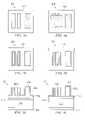
FIGS. 2 a,2b, and2c, afirst pattern 200 is illustrated. Thefirst pattern 200 includes a plurality of line elements. Thefirst pattern 200 is exemplary only and not intended to be limiting, any configuration and quantity of elements providing a pattern is possible. Thefirst pattern 200 may be determined from a layout design file and formed on aphotomask 202. Thephotomask 202 may be a attenuating phase shift mask (att-PSM), an alternating PSM (alt-PSM), a chromeless phase shift mask (CPL), and/or other suitable mask types. Thephotomask 202 includes a substrate. The substrate may be a transparent substrate such as fused silica (SiO2), or quartz, relatively free of defects, calcium fluoride, or other suitable material. Thephotomask 202 may include attenuating material defining the pattern; the attenuating material may include chrome or other materials such as, for example, Au, MoSi, CrN, Mo, Nb2O5, Ti, Ta, MoO3, MoN, Cr2O3, TiN, ZrN, TiO2, TaN, Ta2O5, NbN, Si3N4, ZrN, Al2O3N, Al2O3R, or a combination thereof. FIGS. 2 band2cillustrate asemiconductor substrate 204 including apattern 220 formed thereon. In an embodiment, thesubstrate 204 is silicon in a crystalline structure. In alternative embodiments, thesubstrate 204 may include other elementary semiconductors such as germanium, or includes a compound semiconductor such as, silicon carbide, gallium arsenide, indium arsenide, and indium phosphide. Thepattern 220 is defined by thepattern 200 of thephotomask 202—thepattern 220 is formed using photolithography processing that exposure thesubstrate 204 to thepattern 200.- A
dummy layer 212 is disposed on thesubstrate 204. Thedummy layer 212 may include amorphous carbon, polysilicon, and/or other suitable material. In illustrated embodiments, thedummy layer 212 is the target layer in which the pattern (e.g., half critical dimension features) provided by themethod 100 is to be formed. Numerous other embodiments and layers may be possible. A plurality of hard mask layers210aand210bare disposed on thesubstrate 204. Thedummy layer 208 has been patterned to form a plurality of dummy features having thepattern 220. Thedummy layer 208 may include amorphous carbon, polysilicon, and/or other suitable materials. Aspacer layer 206 is formed on thedummy layer 208. Thespacer layer 206 may include silicon oxide, silicon nitride, silicon oxynitride, and/or other suitable materials. Thespacer layer 206 may define a critical dimension of an element to be formed on thesubstrate 204. For example, in an embodiment thespacer layer 206 will define a width and a pitch for elements formed in thedummy layer 212, as described in greater detail below. The elements in thedummy layer 212 may be used as masking elements in further processing of thesubstrate 204. For example, thedummy layer 212 may be used as a masking element in an etching process of thesubstrate 204, which forms a plurality of fins for a FinFET device. - Thus, the first pattern provides dummy line features which allow for adjacent spacers to be formed. The dummy features, along with the abutting spacers, may define a critical dimension for a feature, such as a fin, to be formed on the substrate.
- The
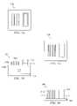
method 100 then proceeds to step104 where a second pattern is provided. The second pattern may remove a portion of a spacer layer overlying dummy line features defined by the pattern ofstep 102. The second pattern may remove a dummy line feature.FIGS. 3 a,3b, and3cillustrate an example. InFIG. 3 a, apattern 300 is formed on aphotomask 302. Thephotomask 302 may be substantially similar to thephotomask 202, described above with reference toFIG. 2 a.FIGS. 3 band3cillustrate a top view and a cross-sectional view of apattern 320 provided on thesubstrate 204. Thepattern 320 is formed by photolithography processes using thepattern 300 of thephotomask 302. Thepattern 300 defines portions of a spacer element to be removed and a plurality of dummy line features to be removed from thesubstrate 204. A plurality ofspacer elements 206bare formed. Thespacer elements 206bmay define a pitch/width for an element of a semiconductor device (e.g., a fin of FinFET). - The
method 100 then proceeds to step106 where a third pattern is provided. The third pattern may be known as a cut pattern or an OD pattern (e.g., defining the active area). The third pattern may remove unwanted spacer elements and/or ends of spacer elements previous formed using the patterns ofsteps FIGS. 4 a,4b, and4cillustrate an example. InFIG. 4 a, apattern 400 is illustrated on aphotomask 402. Thephotomask 402 may be substantially similar to thephotomask 202, described above with reference toFIG. 2 .FIGS. 4 band4cillustrate a top view and a cross-sectional view of apattern 420 provided on thesubstrate 402. Thepattern 420 is formed on thesubstrate 402 by photolithography processes exposing thesubstrate 402 to thepattern 400. Thus, thepattern 420 includes spacer elements having portions at end of the dummy line features removed. One or more spacer elements have also been removed from the substrate204 (e.g., those falling outside the defined active area). Therefore, thepattern 420 includes a grid ofspacer elements 206cformed on thesubstrate 202 in a selected area (e.g., active area). - The
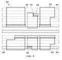
method 100 then proceeds to step108 where the resultant pattern (e.g., the pattern formed from the overlay of the first, second and third patterns described above) is used to process (e.g., etch) the substrate. The resultant pattern forms a masking element. The masking element may be formed by etching a hard mask layer. Referring to the example ofFIGS. 5 aand5b, illustrated are a top view and side view of thesubstrate 204 corresponding to step108. Thehard mask layer 210ahas been patterned using thedummy layer 208 and/or thespacer layer 206c, described above. Thehard mask layer 210amay include silicon nitride, silicon oxynitride, silicon carbide, and/or other suitable dielectric materials. Thedummy layer 208 and thespacer layer 206chave been removed from thesubstrate 204. - The
method 100 may continue to pattern a target dummy layer. The target dummy layer may be patterned to form a grid of masking elements. Referring to the example ofFIGS. 6 aand6b, illustrated are a top view and cross-sectional view of thesubstrate 204. The pattern (e.g., the resultant pattern of the combination of the first, second and third patterns described above) has been formed in thedummy layer 212. In an embodiment, thehard mask 210ais used as a masking element to form the pattern in thedummy layer 212. Thehard mask layer 210ais subsequently removed from thesubstrate 204. Thehard mask layer 210bmay also be patterned simultaneously to and/or prior to the patterning of thedummy layer 212. In alternative embodiments, one or more layers depicted may be omitted such as, thehard mask layer - Therefore, a
patterned dummy layer 212 is formed. As illustrated above, the patterneddummy layer 212, as illustrated inFIGS. 6 aand6b, maybe formed using, successively, first, second, and third patterns each provided in a photomask. The patterned dummy layer212 (and/or thehard mask layer 210b) may be used as a masking element to form devices on thesubstrate 204. In an embodiment, the patterneddummy layer 212 is used as a masking element for forming fins in thesubstrate 204. The fins maybe formed by etching thesubstrate 204. - Referring now to
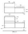
FIG. 7 , illustrated is apattern 700. Thepattern 700 may be provided in a layout design file, a photomask, and/or other suitable means. Thepattern 700 includes afirst pattern 702 and asecond pattern 708. Thefirst pattern 702 includes a grid dummy features706 andcorresponding spacer elements 704. Thefirst pattern 702 may be substantially similar to thepattern 200, described above with reference toFIG. 2 a. Thefirst pattern 702 may be formed on a first photomask and/or defined on a first layer of a layout design file. Thespacer elements 704 may be formed abutting thedummy elements 706. Thesecond pattern 708 may define an active area of a device associated with thepattern 700. Thepattern 708 may be substantially similar to thepattern 400, described above with reference toFIG. 4 a. Thepattern 708 may define an area outside of which theelements - The accurate overlay of the
first pattern 702 and thesecond pattern 708 is to be considered in forming theresultant pattern 700. The overlay process margin (overlay error budget) is represented by W. The overlay margin W may represent the overlay process margin between thefirst pattern 702 and thesecond pattern 708. - In an embodiment, the
dummy feature 706 defines a spacing between fins. Thespacer element 704 may define the width of a fin. In an embodiment, the fin spacing is approximately 27 nanometers. In an embodiment, the fin width is approximately 18 nm. Thus, a pitch of 45 nm may be provided. These dimensions are exemplary only and not intended to be limiting. A patterning pitch of 45 nm may create a small overlay process margin (W) that provides difficulties during fabrication of devices associated with thepattern 700. - Referring now to
FIG. 8 , illustrated is amethod 800 for a determining a layout design of a semiconductor device. Themethod 800, or portions thereof, may be executed by a computer system such as thecomputer system 1500, described below with reference toFIG. 15 . Themethod 800 may increase an overlay process margin, described above with reference toFIG. 7 . Themethod 800 begins atstep 802 where a first pattern is provided. The first pattern generates a global-on-grid pattern of a dummy layer. The first pattern may be substantially similar to the pattern described above with reference to step102 of themethod 100. The first pattern may include a plurality of dummy features in a grid array. The dummy features may allow for spacer elements to be formed abutting the dummy feature. The spacer elements define a pattern having a reduced critical dimension, for example, a critical dimension less (e.g., half) of that provided by the photolithography tool in exposing a photomask. The spacers pitch may define a pitch and/or width of fins to be fabricated on a substrate. FIG. 9 illustrates apattern 900 that includes a global-on-grid pattern ofdummy elements 904.Spacer elements 902 are formed abutting thedummy elements 904.- Referring again to
FIG. 8 , themethod 800 proceeds to step804 where a second pattern is provided. The second pattern may be intended to overlay the first pattern. The second pattern may be substantially similar to the pattern described above with reference to step104 of themethod 100. The second pattern may remove a portion of a spacer element provided by the first pattern. In particular, the second pattern may remove a portion of a spacer element overlying a dummy element of the global-on-grid pattern. - The
method 800 then proceeds to step806 where a third pattern is provided. The third pattern may define an active area of the associated device. The third pattern may overlie (e.g., be intended to be provided subsequently to and aligned with) the first and/or second pattern. The third pattern may remove unwanted ends of the spacer elements formed using the pattern described above instep 802. The third pattern may remove undesired spacer elements and/or line features formed using the pattern described above instep 802. The undesired spacer elements/line features may include those elements lying outside an active area of the associated device. The third pattern may be substantially similar to the pattern described above with reference to step106 of themethod 100. - Referring to the example of
FIG. 9 , apattern 906 is provided. Thepattern 906 is an exemplary embodiment of the third pattern described above with reference to step806. Thepattern 906 defines the active area of the device, for example, defining the areas in which fins (e.g., of a finFet device) are to be formed on the device. - Referring again to
FIG. 8 , themethod 800 then proceeds to step808 where a logic operation procedure is performed on the resultant layout (e.g., the combination/overlay patterns). In an embodiment, the logic operation procedure is performed on the overlay and alignment of the first and third patterns. The logic operation procedure may find one or more locations on the resultant pattern having a critical overlay margin, for example, between the first and third patterns. The critical overlay margin locations may include those locations on the resultant pattern where the margin in error between the overlay of the first and third patterns are insufficient. This margin may be determined by process limitations, design tolerances, etc. The logic operation procedure may be performed using a design rule check (DRC) and/or other suitable methods. - Referring to the example of
FIGS. 9 and 10 , illustrated arelocations 908 having a critical overlay margin. The criticaloverlay margin location 908 may include an edge feature1002 (e.g., a spacer that is to be used to form an edge fin to an active (OD) area). The criticaloverlay margin locations 908 illustrate regions where a bias may be added to the adjacent feature(s) as described in further detail below. - The
method 800 then proceeds to step810 where the first pattern, described above with reference to step802, is modified. The pattern is modified to add bias to dummy line features at locations associated with the identified critical overlay margin areas. Adding bias includes modifying the dimensions of the line. In an embodiment, biasing a feature (e.g., a line feature) includes increasing the width of the feature. The biasing may provide to protect features of the first pattern in the critical overlay margin areas. The biasing may also provide for increased overlay margin in the determined critical overlay margin areas. Thus, in embodiments, the biasing protects edge lines of the pattern (e.g., edge dummy features, spacer elements formed on the edge dummy features, and/or edge fins). - Referring to the example of
FIG. 11 , illustrated is abias portion 1104 added to dummy line features904 in the critical overlay margin areas. Thereference line 1106 illustrates lithography effects (e.g., difference between feature as drawn and as fabricated) typical in forming a pattern on a wafer. Thebias portion 1104 provides an increased overlay margin which may provide for reduced impact of lithography effects and/or more accurate formation of theedge spacer elements 1102. Thebias portion 1104 may be provided by increasing the width of the associateddummy element 904. In an embodiment, thebias portion 1104 is less than approximately 50 nanometers. In an embodiment, thebias portion 1104 is between approximately 3 and 30 nanometers. FIG. 12 illustrates the incorporation of abias region 1204 into selected areas of aline feature 1202. Thebias 1204 provides an increasedoverlay margin 1206 between theline feature 1202 pattern and apattern 1208. The line features1202 may be substantially similar to the dummy line features904, described above with reference toFIGS. 9 ,10, and11. Thepattern 1208 may be substantially similar to thepattern 906, described above with reference toFIGS. 9 ,10, and11. Thus,FIG. 12 illustrates the distortion form a global-on-grid pattern (such as illustrated inpattern 900 ofFIG. 9 ) by the addition of a bias. However, a local-on-grid pattern remains, for example, in the regions defined by thepattern 1208.FIG. 13 illustrates aresultant pattern 1300. Theresultant pattern 1300 includes afirst pattern 1304 and asecond pattern 1302 overlying thefirst pattern 1304. Thefirst pattern 1304 includes a global-on-grid pattern of line elements. Thefirst pattern 1304 may be substantially similar to dummy line features904, described above with reference toFIGS. 9 and 10 . Thefirst pattern 1304 includes a global-on-grid pattern of line elements that may define dummy line features used in a half critical dimension process (such as described above with reference toFIG. 1 ).Spacer elements 1306 may be provided adjacent the line elements of thefirst pattern 1304. Thesecond pattern 1302 may define an active area of a device. In an embodiment, thespacer elements 1306 are provided only within the area defined by thesecond pattern 1302. Thesecond pattern 1302 may be substantially similar to thepattern 906 ofFIGS. 9 and 10 . Theresultant pattern 1300 may be substantially similar to the resultant pattern described above with reference to step808 ofFIG. 8 .FIG. 14 illustrates an embodiment of theresultant pattern 1300 after a bias has been applied, for example, after thestep 810 of themethod 800 has been applied to the layout design. Thebiased pattern 1400 includes afirst pattern 1402. Thefirst pattern 1402 includes a local-on-grid pattern of line elements within an area defined by asecond pattern 1404. These local-on-grid line elements providespacer elements 1406 that allow for on-grid pitch with a localized area. Thespacer elements 1406 may be used to form fin elements of a device. Thefirst pattern 1402 also includes lines having bias regions as illustrated byline section 1408. Theresultant pattern 1400 including its local-on-grid pattern may be used in the formation of a semiconductor device. In an embodiment, thefirst pattern 1402 and thesecond pattern 1404 may be used insteps method 100, respectively.- One system for providing the disclosed embodiments is illustrated in
FIG. 15 . Illustrated is an embodiment of acomputer system 1500 for implementing embodiments of the present disclosure including the systems and methods described herein. In an embodiment, thecomputer system 1500 includes functionality providing for one or more steps of designing a circuit or chip including performing simulations, verification analysis (e.g., DRC, LVS), extraction of parameters, layout, place and route, DFM, and/or other suitable tools and/or procedures. - The
computer system 1500 includes amicroprocessor 1504, aninput device 1510, astorage device 1506, asystem memory 1508, adisplay 1514, and acommunication device 1512 all interconnected by one ormore buses 1502. Thestorage device 1506 may be a floppy drive, hard drive, CD-ROM, optical device or any other storage device. In addition, thestorage device 1506 may be capable of receiving a floppy disk, CD-ROM, DVD-ROM, or any other form of computer-readable medium that may contain computer-executable instructions. Thecommunications device 1512 may be a modem, a network card, or any other device to enable the computer system to communicate with other nodes. It is understood that anycomputer system 1500 could represent a plurality of interconnected computer systems such as, personal computers, mainframes, PDAs, and telephonic devices. - The
computer system 1500 includes hardware capable of executing machine-readable instructions as well as the software for executing acts (typically machine-readable instructions) that produce a desired result. Software includes any machine code stored in any memory medium, such as RAM or ROM, and machine code stored on other storage devices (such as floppy disks, flash memory, or a CD ROM, for example). Software may include source or object code, for example. In additional software encompasses any set of instructions capable of being executed in a client machine or server. Any combination of hardware and software may comprise a computer system. Thesystem memory 1508 may be configured to store a design database, library, technology files, design rules, PDKs, models, decks, and/or other information used in the design of a semiconductor device. - Computer readable mediums include passive data storage, such as RAM as well as semi-permanent data storage such as a compact disk read only memory (CD-ROM). In an embodiment of the present disclosure may be embodied in the RAM of a computer to transform a standard computer into a new specific computing machine. Data structures are defined organizations of data that may enable an embodiment of the present disclosure. For example, a data structure may provide an organization of data, or an organization of executable code. Data signals could be carried across transmission mediums and store and transport various data structures, and thus, may be used to transport an embodiment of the present disclosure.
- The
computer system 1500 may be used to implement one or more of the methods and/or devices described herein. In particular, thecomputer system 1500 may be operable to generate, store, manipulate, and/or perform other actions on a layout pattern (e.g., GDSII file) associated with an integrated circuit. For example, in an embodiment, one or more of the patterns described above may be generated, manipulated, and/or stored using thecomputer system 1500. The patterns provided by thecomputer system 1500 may be in a typical layout design file format which are communicated to one or more other computer systems for use in fabricating photomasks including the defined patterns.
Claims (20)
1. A method, comprising:
providing a first pattern, wherein the first pattern comprises an array of dummy line features and a plurality of spacer elements abutting the dummy line features;
providing a second pattern, wherein the second pattern defines an active region of an integrated circuit device;
determining an edge spacer element of the plurality of spacer elements of the first pattern, wherein the edge spacer element is a spacer element nearest an edge of the active region; and
biasing a first dummy line feature of the array of dummy line features, wherein the first dummy line feature is adjacent an edge spacer element and outside the active region.
2. The method ofclaim 1 , wherein the biasing the first dummy line feature comprises increasing the width of the first dummy line feature.
3. The method ofclaim 1 , wherein the integrated circuit device includes a plurality of FinFET devices and wherein the array of dummy line features defines a pitch of the fins of the plurality of FinFet devices.
4. The method ofclaim 1 , wherein the integrated circuit device includes a plurality of FinFET devices and wherein the spacer elements define a width of the fins of the plurality of FinFet devices.
5. The method ofclaim 1 , wherein the array of dummy line features of the first pattern is a global-on-grid array of dummy line features, and wherein the biasing the first dummy line produces a modified first pattern, wherein the modified first pattern includes a plurality of localized-on-grid arrays of dummy line features.
6. The method ofclaim 1 , wherein the determining the edge spacer element of the active region includes performing a logic operation procedure.
7. The method ofclaim 1 , wherein the determining the edge spacer element of the active region includes identifying a location on the integrated circuit layout wherein an overlay offset margin between the first pattern and the second pattern is below a selected value.
8. A method, comprising:
generating a first layout pattern and a second layout pattern for an integrated circuit, wherein the first pattern includes a global-on-grid array of dummy line features, and wherein the dummy line features define a pitch for fins of a plurality of finFet devices;
performing a logic operation procedure on the first layout pattern and the second layout pattern, wherein the logic operation procedure identifies a location having a critical overlay margin between the first layout pattern and the second layout pattern; and
generating a third pattern, wherein the generating the third pattern includes modifying the first layout pattern in response to the location having the critical overlay margin, wherein the modifying comprises biasing a first dummy line feature, wherein the first dummy line feature is outside an area defined by the second layout pattern.
9. The method ofclaim 8 , further comprising:
using the third pattern to generate a first photomask associated with the integrated circuit device; and
using the second pattern to generate a second photomask associated with the integrated circuit device.
10. The method ofclaim 8 , further comprising:
exposing a semiconductor substrate to the third pattern; and
exposing the semiconductor substrate to the second pattern, after the substrate has been exposed to the third pattern.
11. The method ofclaim 8 , further comprising:
using the third pattern to generate an array of dummy features on a semiconductor substrate; and
using the second pattern to remove at least one dummy feature generated by the third pattern from the semiconductor substrate.
12. The method ofclaim 8 , wherein the third pattern and the second pattern have a greater overlay margin than the first pattern and the second pattern.
13. The method ofclaim 8 , further comprising:
providing a semiconductor substrate;
forming a dummy layer on the semiconductor substrate;
exposing the semiconductor substrate to the third pattern to form a plurality of dummy line features in the dummy layer;
depositing a spacer material on the plurality of dummy line features;
etching the spacer material to form spacer elements adjacent the dummy line features; and
exposing the substrate including the spacer elements to the second pattern to define an active area.
14. The method ofclaim 8 , further comprising:
forming a final layout for the integrated circuit device, wherein the final layout includes the third pattern and the second pattern, and wherein the final layout includes a grid array of dummy line features in an area defined by the second pattern.
15. An apparatus comprising a computer-readable medium encoded with a computer program that, when executed:
provides a first layout pattern and a second layout pattern for an integrated circuit, wherein the first pattern includes a global-on-grid array of dummy line features, and wherein the dummy line features define a pitch for fins of a plurality of finFet devices;
performs a logic operation procedure on the first layout pattern and the second layout pattern, wherein the logic operation procedure identifies a location having a critical overlay margin between the first layout pattern and the second layout pattern; and
modifies the first layout pattern in response to the location having the critical overlay margin, wherein the modifying comprises biasing a first dummy line feature, wherein the first dummy line feature is outside an area defined by the second layout pattern.
16. The apparatus ofclaim 15 , wherein the modified first layout pattern includes local-on-grid arrays of dummy line features inside an area defined by the second layout pattern.
17. The apparatus ofclaim 15 , wherein the first feature is a dummy line adjacent an edge feature of the first layout pattern, wherein the edge feature includes a spacer element at an edge of an active area defined by the second pattern.
18. The apparatus ofclaim 15 , wherein the biasing includes increasing the width of the dummy line feature.
19. The apparatus ofclaim 15 , further comprising a computer program that when executed:
sends the modified first pattern and the second pattern to a tool associated with photomask fabrication.
20. The apparatus ofclaim 15 , wherein the biasing includes increasing the width of the dummy line feature by between approximately 3 and 30 nanometers.
Priority Applications (3)
| Application Number | Priority Date | Filing Date | Title |
|---|---|---|---|
| US12/356,405US7862962B2 (en) | 2009-01-20 | 2009-01-20 | Integrated circuit layout design |
| US12/980,764US8039179B2 (en) | 2009-01-20 | 2010-12-29 | Integrated circuit layout design |
| US13/248,932US8241823B2 (en) | 2009-01-20 | 2011-09-29 | Method of fabrication of a semiconductor device having reduced pitch |
Applications Claiming Priority (1)
| Application Number | Priority Date | Filing Date | Title |
|---|---|---|---|
| US12/356,405US7862962B2 (en) | 2009-01-20 | 2009-01-20 | Integrated circuit layout design |
Related Child Applications (1)
| Application Number | Title | Priority Date | Filing Date |
|---|---|---|---|
| US12/980,764ContinuationUS8039179B2 (en) | 2009-01-20 | 2010-12-29 | Integrated circuit layout design |
Publications (2)
| Publication Number | Publication Date |
|---|---|
| US20100183961A1true US20100183961A1 (en) | 2010-07-22 |
| US7862962B2 US7862962B2 (en) | 2011-01-04 |
Family
ID=42337222
Family Applications (3)
| Application Number | Title | Priority Date | Filing Date |
|---|---|---|---|
| US12/356,405Expired - Fee RelatedUS7862962B2 (en) | 2009-01-20 | 2009-01-20 | Integrated circuit layout design |
| US12/980,764ActiveUS8039179B2 (en) | 2009-01-20 | 2010-12-29 | Integrated circuit layout design |
| US13/248,932ActiveUS8241823B2 (en) | 2009-01-20 | 2011-09-29 | Method of fabrication of a semiconductor device having reduced pitch |
Family Applications After (2)
| Application Number | Title | Priority Date | Filing Date |
|---|---|---|---|
| US12/980,764ActiveUS8039179B2 (en) | 2009-01-20 | 2010-12-29 | Integrated circuit layout design |
| US13/248,932ActiveUS8241823B2 (en) | 2009-01-20 | 2011-09-29 | Method of fabrication of a semiconductor device having reduced pitch |
Country Status (1)
| Country | Link |
|---|---|
| US (3) | US7862962B2 (en) |
Cited By (58)
| Publication number | Priority date | Publication date | Assignee | Title |
|---|---|---|---|---|
| US20070228372A1 (en)* | 2004-10-19 | 2007-10-04 | Taiwan Semiconductor Manufacturing Company, Ltd. | Method for Fabricating a Body Contact in a Finfet Structure and a Device Including the Same |
| US20090035909A1 (en)* | 2007-07-31 | 2009-02-05 | Taiwan Semiconductor Manufacturing Company, Ltd. | Method of fabrication of a finfet element |
| US20100006945A1 (en)* | 2008-06-11 | 2010-01-14 | Taiwan Semiconductor Manufacturing Company, Ltd. | Finfet drive strength modification |
| US20100052059A1 (en)* | 2008-08-28 | 2010-03-04 | Taiwan Semiconductor Manufacturing Company, Ltd. | Finfet process compatible native transistor |
| US20100203734A1 (en)* | 2009-02-12 | 2010-08-12 | Taiwan Semiconductor Manufacturing Company, Ltd. | Method of pitch halving |
| US20100264468A1 (en)* | 2009-04-17 | 2010-10-21 | Taiwan Semiconductor Manufacturing Company, Ltd. | Method Of Fabrication Of A FinFET Element |
| US20100292963A1 (en)* | 2009-04-15 | 2010-11-18 | James Schroeder | Personal fit medical implants and orthopedic surgical instruments and methods for making |
| US20100296213A1 (en)* | 2009-02-19 | 2010-11-25 | Jam-Wem Lee | ESD Protection for FinFETs |
| US20110101421A1 (en)* | 2009-10-30 | 2011-05-05 | Taiwan Semiconductor Manufacturing Company, Ltd. | Method of forming epi film in substrate trench |
| US20110117679A1 (en)* | 2009-11-19 | 2011-05-19 | Taiwan Semiconductor Manufacturing Company, Ltd. | Sacrificial offset protection film for a finfet device |
| US20110151359A1 (en)* | 2009-01-20 | 2011-06-23 | Taiwan Semiconductor Manufacturing Company, Ltd. | Integrated circuit layout design |
| US20110147846A1 (en)* | 2009-12-22 | 2011-06-23 | Taiwan Semiconductor Manufacturing Company, Ltd | Method for incorporating impurity element in epi silicon process |
| US20110156148A1 (en)* | 2009-12-30 | 2011-06-30 | Taiwan Semiconductor Manufacturing Co., Ltd. | Semiconductor device and method for making the same using semiconductor fin density design rules |
| US20110193141A1 (en)* | 2010-02-11 | 2011-08-11 | Taiwan Semiconductor Manufacturing Company, Ltd. | Method of fabricating a finfet device |
| US8062963B1 (en) | 2010-10-08 | 2011-11-22 | Taiwan Semiconductor Manufacturing Company, Ltd. | Method of fabricating a semiconductor device having an epitaxy region |
| US20120094492A1 (en)* | 2010-10-13 | 2012-04-19 | Dong-Woon Park | Method of forming pattern, reticle, and computer readable medium for storing program for forming pattern |
| US20120124528A1 (en)* | 2010-11-12 | 2012-05-17 | Taiwan Semiconductor Manufacturing Company, Ltd. | Method and device for increasing fin device density for unaligned fins |
| US8212295B2 (en) | 2010-06-30 | 2012-07-03 | Taiwan Semiconductor Manufacturing Company, Ltd. | ROM cell circuit for FinFET devices |
| US8278173B2 (en) | 2010-06-30 | 2012-10-02 | Taiwan Semiconductor Manufacturing Company, Ltd. | Method of fabricating gate structures |
| US8278196B2 (en) | 2010-07-21 | 2012-10-02 | Taiwan Semiconductor Manufacturing Company, Ltd. | High surface dopant concentration semiconductor device and method of fabricating |
| US8286114B2 (en) | 2007-04-18 | 2012-10-09 | Taiwan Semiconductor Manufacturing Company, Ltd. | 3-dimensional device design layout |
| US8338305B2 (en) | 2010-10-19 | 2012-12-25 | Taiwan Semiconductor Manufacturing Company, Ltd. | Multi-fin device by self-aligned castle fin formation |
| US8357569B2 (en) | 2009-09-29 | 2013-01-22 | Taiwan Semiconductor Manufacturing Company, Ltd. | Method of fabricating finfet device |
| US8367498B2 (en) | 2010-10-18 | 2013-02-05 | Taiwan Semiconductor Manufacturing Company, Ltd. | Fin-like field effect transistor (FinFET) device and method of manufacturing same |
| US8373229B2 (en) | 2010-08-30 | 2013-02-12 | Taiwan Semiconductor Manufacturing Company, Ltd. | Gate controlled bipolar junction transistor on fin-like field effect transistor (FinFET) structure |
| US20130052793A1 (en)* | 2011-08-25 | 2013-02-28 | Taiwan Semiconductor Manufacturing Company, Ltd. | Layer Alignment in FinFET Fabrication |
| US8399931B2 (en) | 2010-06-30 | 2013-03-19 | Taiwan Semiconductor Manufacturing Company, Ltd. | Layout for multiple-fin SRAM cell |
| US8431453B2 (en) | 2011-03-31 | 2013-04-30 | Taiwan Semiconductor Manufacturing Company, Ltd. | Plasma doping to reduce dielectric loss during removal of dummy layers in a gate structure |
| US8482073B2 (en) | 2010-03-25 | 2013-07-09 | Taiwan Semiconductor Manufacturing Company, Ltd. | Integrated circuit including FINFETs and methods for forming the same |
| US8486769B2 (en) | 2010-11-19 | 2013-07-16 | Taiwan Semiconductor Manufacturing Company, Ltd. | Method for forming metrology structures from fins in integrated circuitry |
| US20130217233A1 (en)* | 2012-02-22 | 2013-08-22 | Taiwan Semiconductor Manufacturing Company, Ltd. | Methods for Controlling Line Dimensions in Spacer Alignment Double Patterning Semiconductor Processing |
| US8525267B2 (en) | 2010-11-23 | 2013-09-03 | Taiwan Semiconductor Manufacturing Company, Ltd. | Device and method for forming Fins in integrated circuitry |
| US20130239077A1 (en)* | 2012-03-08 | 2013-09-12 | Taiwan Semiconductor Manufacturing Company, Ltd. | LVS Implementation for FinFET Design |
| US20130273711A1 (en)* | 2012-04-17 | 2013-10-17 | Taiwan Semiconductor Manufacturing Company, Ltd. | Method of forming a finfet device |
| US8609495B2 (en) | 2010-04-08 | 2013-12-17 | Taiwan Semiconductor Manufacturing Company, Ltd. | Hybrid gate process for fabricating finfet device |
| US8621398B2 (en) | 2010-05-14 | 2013-12-31 | Taiwan Semiconductor Manufacturing Company, Ltd. | Automatic layout conversion for FinFET device |
| US8629478B2 (en) | 2009-07-31 | 2014-01-14 | Taiwan Semiconductor Manufacturing Company, Ltd. | Fin structure for high mobility multiple-gate transistor |
| US8633076B2 (en) | 2010-11-23 | 2014-01-21 | Taiwan Semiconductor Manufacturing Company, Ltd. | Method for adjusting fin width in integrated circuitry |
| US8675397B2 (en) | 2010-06-25 | 2014-03-18 | Taiwan Semiconductor Manufacturing Company, Ltd. | Cell structure for dual-port SRAM |
| US8729627B2 (en) | 2010-05-14 | 2014-05-20 | Taiwan Semiconductor Manufacturing Company, Ltd. | Strained channel integrated circuit devices |
| US8796124B2 (en) | 2011-10-25 | 2014-08-05 | Taiwan Semiconductor Manufacturing Company, Ltd. | Doping method in 3D semiconductor device |
| US8796156B2 (en) | 2009-10-27 | 2014-08-05 | Taiwan Semiconductor Manufacturing Company, Ltd. | Cross OD FinFET patterning |
| US8796759B2 (en) | 2010-07-15 | 2014-08-05 | Taiwan Semiconductor Manufacturing Company, Ltd. | Fin-like field effect transistor (FinFET) device and method of manufacturing same |
| US8809940B2 (en) | 2010-10-13 | 2014-08-19 | Taiwan Semiconductor Manufacturing Company, Ltd. | Fin held effect transistor |
| US8881084B2 (en) | 2010-05-14 | 2014-11-04 | Taiwan Semiconductor Manufacturing Company, Ltd. | FinFET boundary optimization |
| US8942030B2 (en) | 2010-06-25 | 2015-01-27 | Taiwan Semiconductor Manufacturing Company, Ltd. | Structure and method for SRAM cell circuit |
| US8980719B2 (en) | 2010-04-28 | 2015-03-17 | Taiwan Semiconductor Manufacturing Company, Ltd. | Methods for doping fin field-effect transistors |
| US9130058B2 (en) | 2010-07-26 | 2015-09-08 | Taiwan Semiconductor Manufacturing Company, Ltd. | Forming crown active regions for FinFETs |
| US9166022B2 (en) | 2010-10-18 | 2015-10-20 | Taiwan Semiconductor Manufacturing Company, Ltd. | Fin-like field effect transistor (FinFET) device and method of manufacturing same |
| TWI506792B (en)* | 2012-06-13 | 2015-11-01 | Synopsys Inc | N-channel and P-channel end-to-end fin field effect transistor (FinFET) cell architecture with loose gate spacing |
| US20160027776A1 (en)* | 2014-03-05 | 2016-01-28 | International Business Machines Corporation | Densely spaced fins for semiconductor fin field effect transistors |
| US20160211262A1 (en)* | 2013-09-25 | 2016-07-21 | Walid M. Hafez | Isolation well doping with solid-state diffusion sources for finfet architectures |
| US9472550B2 (en) | 2010-11-23 | 2016-10-18 | Taiwan Semiconductor Manufacturing Company, Ltd. | Adjusted fin width in integrated circuitry |
| KR20180032505A (en)* | 2016-09-22 | 2018-03-30 | 삼성전자주식회사 | Method for high performance standard cell design techniques in finfet based library using local layout effects (lle) |
| DE102015104473B4 (en)* | 2014-05-15 | 2021-05-27 | Taiwan Semiconductor Manufacturing Co., Ltd. | RETICLE AND METHOD OF ITS MANUFACTURING |
| CN113658937A (en)* | 2021-08-11 | 2021-11-16 | 福建省晋华集成电路有限公司 | Semiconductor structure, method of making the same, and method of making a semiconductor layout |
| US11222947B2 (en) | 2015-09-25 | 2022-01-11 | Intel Corporation | Methods of doping fin structures of non-planar transistor devices |
| US20220197129A1 (en)* | 2020-12-22 | 2022-06-23 | Taiwan Semiconductor Manufacturing Company Ltd | Methods for making semiconductor-based integrated circuits |
Families Citing this family (74)
| Publication number | Priority date | Publication date | Assignee | Title |
|---|---|---|---|---|
| US10192859B2 (en) | 2011-05-11 | 2019-01-29 | Texas Instruments Incorporated | Integrated circuits and processes for protection of standard cell performance from context effects |
| US8561003B2 (en) | 2011-07-29 | 2013-10-15 | Synopsys, Inc. | N-channel and P-channel finFET cell architecture with inter-block insulator |
| US8595661B2 (en) | 2011-07-29 | 2013-11-26 | Synopsys, Inc. | N-channel and p-channel finFET cell architecture |
| US9059001B2 (en) | 2011-12-16 | 2015-06-16 | Taiwan Semiconductor Manufacturing Company, Ltd. | Semiconductor device with biased feature |
| US8741776B2 (en)* | 2012-02-07 | 2014-06-03 | Taiwan Semiconductor Manufacturing Company, Ltd. | Patterning process for fin-like field effect transistor (finFET) device |
| US9252021B2 (en) | 2012-02-09 | 2016-02-02 | Taiwan Semiconductor Manufacturing Company, Ltd. | Method for patterning a plurality of features for Fin-like field-effect transistor (FinFET) devices |
| US9236267B2 (en) | 2012-02-09 | 2016-01-12 | Taiwan Semiconductor Manufacturing Company, Ltd. | Cut-mask patterning process for fin-like field effect transistor (FinFET) device |
| US8901615B2 (en) | 2012-06-13 | 2014-12-02 | Synopsys, Inc. | N-channel and P-channel end-to-end finfet cell architecture |
| US9147694B2 (en)* | 2012-11-30 | 2015-09-29 | Taiwan Semiconductor Manufacturing Company Limited | Density gradient cell array |
| US8910094B2 (en)* | 2013-02-06 | 2014-12-09 | Globalfoundries Inc. | Retargeting semiconductor device shapes for multiple patterning processes |
| US8869090B2 (en)* | 2013-03-11 | 2014-10-21 | Taiwan Semiconductor Manufacturing Company, Ltd. | Stretch dummy cell insertion in FinFET process |
| US9184101B2 (en) | 2013-03-11 | 2015-11-10 | Taiwan Semiconductor Manufacturing Co., Ltd. | Method for removing semiconductor fins using alternating masks |
| US9147029B2 (en)* | 2013-03-11 | 2015-09-29 | Taiwan Semiconductor Manufacturing Company, Ltd. | Stretch dummy cell insertion in FinFET process |
| US8846490B1 (en) | 2013-03-12 | 2014-09-30 | Taiwan Semiconductor Manufacturing Company, Ltd. | Method of fabricating a FinFET device |
| US8932957B2 (en) | 2013-03-12 | 2015-01-13 | Taiwan Semiconductor Manufacturing Company, Ltd. | Method of fabricating a FinFET device |
| US9054159B2 (en) | 2013-03-14 | 2015-06-09 | Taiwan Semiconductor Manufacturing Company, Ltd. | Method of patterning a feature of a semiconductor device |
| US9076736B2 (en) | 2013-03-14 | 2015-07-07 | Taiwan Semiconductor Manufacturing Company, Ltd. | Patterning method for semiconductor device fabrication |
| US8835323B1 (en) | 2013-03-14 | 2014-09-16 | Taiwan Semiconductor Manufacturing Company, Ltd. | Method for integrated circuit patterning |
| US9153478B2 (en) | 2013-03-15 | 2015-10-06 | Taiwan Semiconductor Manufacturing Company, Ltd. | Spacer etching process for integrated circuit design |
| US9009633B2 (en)* | 2013-05-06 | 2015-04-14 | United Microelectronics Corp. | Method of correcting assist feature |
| US9764950B2 (en) | 2013-08-16 | 2017-09-19 | Taiwan Semiconductor Manufacturing Company Limited | Semiconductor arrangement with one or more semiconductor columns |
| US8987008B2 (en) | 2013-08-20 | 2015-03-24 | Taiwan Semiconductor Manufacturing Company, Ltd. | Integrated circuit layout and method with double patterning |
| US9929153B2 (en) | 2013-10-18 | 2018-03-27 | Taiwan Semiconductor Manufacturing Company, Ltd. | Method of making a FinFET device |
| US9034723B1 (en) | 2013-11-25 | 2015-05-19 | Taiwan Semiconductor Manufacturing Company, Ltd. | Method of making a FinFET device |
| US9761436B2 (en) | 2014-06-30 | 2017-09-12 | Taiwan Semiconductor Manufacturing Company, Ltd. | Mechanisms for forming patterns using multiple lithography processes |
| US10163652B2 (en) | 2014-03-13 | 2018-12-25 | Taiwan Semiconductor Manufacturing Company, Ltd. | Mechanisms for forming patterns using multiple lithography processes |
| US9293341B2 (en) | 2014-03-13 | 2016-03-22 | Taiwan Semiconductor Manufacturing Company, Ltd. | Mechanisms for forming patterns using multiple lithography processes |
| US9245763B2 (en)* | 2014-03-13 | 2016-01-26 | Taiwan Semiconductor Manufacturing Company, Ltd. | Mechanisms for forming patterns using multiple lithography processes |
| US9740092B2 (en)* | 2014-08-25 | 2017-08-22 | Globalfoundries Inc. | Model-based generation of dummy features |
| US9941139B2 (en) | 2014-09-10 | 2018-04-10 | Taiwan Semiconductor Manufacturing Company, Ltd. | Method of semiconductor integrated circuit fabrication |
| CN105719688B (en)* | 2014-12-04 | 2019-03-29 | 中芯国际集成电路制造(上海)有限公司 | SRAM memory and the method for forming SRAM memory |
| US9472414B2 (en) | 2015-02-13 | 2016-10-18 | Taiwan Semiconductor Manufacturing Company, Ltd. | Self-aligned multiple spacer patterning process |
| US9449880B1 (en)* | 2015-02-26 | 2016-09-20 | Taiwan Semiconductor Manufacturing Company, Ltd. | Fin patterning methods for increased process margin |
| US9418868B1 (en) | 2015-03-13 | 2016-08-16 | Taiwan Semiconductor Manufacturing Company, Ltd. | Method of fabricating semiconductor device with reduced trench distortions |
| US9711369B2 (en) | 2015-03-16 | 2017-07-18 | Taiwan Semiconductor Manufacturing Company, Ltd. | Method for forming patterns with sharp jogs |
| US9703918B2 (en) | 2015-03-16 | 2017-07-11 | Taiwan Semiconductor Manufacturing Company, Ltd. | Two-dimensional process window improvement |
| US9991132B2 (en) | 2015-04-17 | 2018-06-05 | Taiwan Semiconductor Manufacturing Company, Ltd. | Lithographic technique incorporating varied pattern materials |
| US9530660B2 (en) | 2015-05-15 | 2016-12-27 | Taiwan Semiconductor Manufacturing Company, Ltd. | Multiple directed self-assembly patterning process |
| US9946827B2 (en) | 2015-07-16 | 2018-04-17 | Taiwan Semiconductor Manufacturing Company, Ltd. | Method and structure for mandrel and spacer patterning |
| US9589890B2 (en) | 2015-07-20 | 2017-03-07 | Taiwan Semiconductor Manufacturing Company, Ltd. | Method for interconnect scheme |
| US10008382B2 (en) | 2015-07-30 | 2018-06-26 | Taiwan Semiconductor Manufacturing Company, Ltd. | Semiconductor device having a porous low-k structure |
| US9627215B1 (en) | 2015-09-25 | 2017-04-18 | Taiwan Semiconductor Manufacturing Company, Ltd. | Structure and method for interconnection |
| US9728407B2 (en) | 2015-12-30 | 2017-08-08 | Taiwan Semiconductor Manufacturing Company, Ltd. | Method of forming features with various dimensions |
| US10084040B2 (en) | 2015-12-30 | 2018-09-25 | Taiwan Semiconductor Manufacturing Co., Ltd. | Seamless gap fill |
| US9711604B1 (en) | 2015-12-31 | 2017-07-18 | Taiwan Semiconductor Manufacturing Co., Ltd. | Loading effect reduction through multiple coat-etch processes |
| US10157742B2 (en) | 2015-12-31 | 2018-12-18 | Taiwan Semiconductor Manufacturing Co., Ltd. | Method for mandrel and spacer patterning |
| US9935199B2 (en) | 2016-01-15 | 2018-04-03 | Taiwan Semiconductor Manufacturing Company, Ltd. | FinFET with source/drain structure |
| US9570302B1 (en) | 2016-02-10 | 2017-02-14 | Taiwan Semiconductor Manufacturing Co., Ltd. | Method of patterning a material layer |
| US9684236B1 (en) | 2016-03-17 | 2017-06-20 | Taiwan Semiconductor Manufacturing Co., Ltd. | Method of patterning a film layer |
| US9911611B2 (en) | 2016-03-17 | 2018-03-06 | Taiwan Semiconductor Manufacturing Company, Ltd. | Method of forming openings in a material layer |
| US9799529B2 (en) | 2016-03-17 | 2017-10-24 | Taiwan Semiconductor Manufacturing Co., Ltd. | Method of planarizing a film layer |
| US10056265B2 (en) | 2016-03-18 | 2018-08-21 | Taiwan Semiconductor Manufacturing Co., Ltd. | Directed self-assembly process with size-restricted guiding patterns |
| US9911606B2 (en) | 2016-04-28 | 2018-03-06 | Taiwan Semiconductor Manufacturing Co., Ltd. | Mandrel spacer patterning in multi-pitch integrated circuit manufacturing |
| US10147649B2 (en) | 2016-05-27 | 2018-12-04 | Taiwan Semiconductor Manufacturing Co., Ltd. | Semiconductor device structure with gate stack and method for forming the same |
| US9768061B1 (en) | 2016-05-31 | 2017-09-19 | Taiwan Semiconductor Manufacturing Co., Ltd. | Low-k dielectric interconnect systems |
| US10032639B2 (en) | 2016-05-31 | 2018-07-24 | Taiwan Semiconductor Manufacturing Company, Ltd. | Methods for improved critical dimension uniformity in a semiconductor device fabrication process |
| US10361286B2 (en) | 2016-06-24 | 2019-07-23 | Taiwan Semiconductor Manufacturing Co., Ltd. | Method and structure for mandrel and spacer patterning |
| US9972526B2 (en) | 2016-07-29 | 2018-05-15 | Taiwan Semiconductor Manufacturing Co., Ltd. | Method for forming conductive structure in semiconductor structure |
| US10229832B2 (en)* | 2016-09-22 | 2019-03-12 | Varian Semiconductor Equipment Associates, Inc. | Techniques for forming patterned features using directional ions |
| US10282504B2 (en) | 2016-09-30 | 2019-05-07 | Taiwan Semiconductor Manufacturing Co., Ltd. | Method for improving circuit layout for manufacturability |
| US10446662B2 (en) | 2016-10-07 | 2019-10-15 | Taiwan Semiconductor Manufacturing Co., Ltd. | Reducing metal gate overhang by forming a top-wide bottom-narrow dummy gate electrode |
| US10020261B2 (en) | 2016-10-14 | 2018-07-10 | Taiwan Semiconductor Manufacturing Co., Ltd. | Split rail structures located in adjacent metal layers |
| US10020379B2 (en) | 2016-11-18 | 2018-07-10 | Taiwan Semiconuctor Manufacturing Co., Ltd. | Method for forming semiconductor device structure using double patterning |
| US10957529B2 (en) | 2016-11-28 | 2021-03-23 | Taiwan Semiconductor Manufacturing Co., Ltd. | Method for drying wafer with gaseous fluid |
| US9881794B1 (en) | 2016-11-29 | 2018-01-30 | Taiwan Semiconductor Manufacturing Company, Ltd. | Semiconductor methods and devices |
| US11901190B2 (en)* | 2017-11-30 | 2024-02-13 | Taiwan Semiconductor Manufacturing Company, Ltd. | Method of patterning |
| US11054742B2 (en) | 2018-06-15 | 2021-07-06 | Taiwan Semiconductor Manufacturing Co., Ltd. | EUV metallic resist performance enhancement via additives |
| US11069526B2 (en) | 2018-06-27 | 2021-07-20 | Taiwan Semiconductor Manufacturing Co., Ltd. | Using a self-assembly layer to facilitate selective formation of an etching stop layer |
| US10867805B2 (en) | 2018-06-29 | 2020-12-15 | Taiwan Semiconductor Manufacturing Co., Ltd. | Selective removal of an etching stop layer for improving overlay shift tolerance |
| US11069793B2 (en) | 2018-09-28 | 2021-07-20 | Taiwan Semiconductor Manufacturing Co., Ltd. | Reducing parasitic capacitance for gate-all-around device by forming extra inner spacers |
| DE102019117786B4 (en) | 2018-09-28 | 2022-05-12 | Taiwan Semiconductor Manufacturing Co., Ltd. | REDUCING PARASITIC CAPACITY FOR GATE ALL AROUND DEVICE BY FORMING ADDITIONAL INTERNAL SPACERS |
| US11527444B2 (en) | 2019-09-25 | 2022-12-13 | Taiwan Semiconductor Manufacturing Co., Ltd. | Air spacer formation for semiconductor devices |
| US11502182B2 (en) | 2020-05-11 | 2022-11-15 | Taiwan Semiconductor Manufacturing Co., Ltd. | Selective gate air spacer formation |
| US12132105B2 (en) | 2021-04-02 | 2024-10-29 | Samsung Electronics Co., Ltd. | Semiconductor device and method for fabricating the same |
Citations (6)
| Publication number | Priority date | Publication date | Assignee | Title |
|---|---|---|---|---|
| US6706571B1 (en)* | 2002-10-22 | 2004-03-16 | Advanced Micro Devices, Inc. | Method for forming multiple structures in a semiconductor device |
| US6858478B2 (en)* | 2002-08-23 | 2005-02-22 | Intel Corporation | Tri-gate devices and methods of fabrication |
| US20050153490A1 (en)* | 2003-12-16 | 2005-07-14 | Jae-Man Yoon | Method of forming fin field effect transistor |
| US7190050B2 (en)* | 2005-07-01 | 2007-03-13 | Synopsys, Inc. | Integrated circuit on corrugated substrate |
| US20080179705A1 (en)* | 2007-01-31 | 2008-07-31 | Christoph Noelscher | Semiconductor device, method for manufacturing a semiconductor device and mask for manufacturing a semiconductor device |
| US20100183958A1 (en)* | 2009-01-21 | 2010-07-22 | Kabushiki Kaisha Toshiba | Method of fabricating semiconductor device, and photomask |
Family Cites Families (22)
| Publication number | Priority date | Publication date | Assignee | Title |
|---|---|---|---|---|
| CN1193355C (en)* | 2000-05-17 | 2005-03-16 | 日本胜利株式会社 | Information recording medium and recording method thereof |
| US6734107B2 (en)* | 2002-06-12 | 2004-05-11 | Macronix International Co., Ltd. | Pitch reduction in semiconductor fabrication |
| US7989855B2 (en)* | 2004-06-10 | 2011-08-02 | Nec Corporation | Semiconductor device including a deflected part |
| US7115525B2 (en)* | 2004-09-02 | 2006-10-03 | Micron Technology, Inc. | Method for integrated circuit fabrication using pitch multiplication |
| US7244640B2 (en)* | 2004-10-19 | 2007-07-17 | Taiwan Semiconductor Manufacturing Company, Ltd. | Method for fabricating a body contact in a Finfet structure and a device including the same |
| US7253118B2 (en)* | 2005-03-15 | 2007-08-07 | Micron Technology, Inc. | Pitch reduced patterns relative to photolithography features |
| US7508031B2 (en)* | 2005-07-01 | 2009-03-24 | Synopsys, Inc. | Enhanced segmented channel MOS transistor with narrowed base regions |
| US7807523B2 (en)* | 2005-07-01 | 2010-10-05 | Synopsys, Inc. | Sequential selective epitaxial growth |
| US7605449B2 (en)* | 2005-07-01 | 2009-10-20 | Synopsys, Inc. | Enhanced segmented channel MOS transistor with high-permittivity dielectric isolation material |
| US8466490B2 (en)* | 2005-07-01 | 2013-06-18 | Synopsys, Inc. | Enhanced segmented channel MOS transistor with multi layer regions |
| US7247887B2 (en)* | 2005-07-01 | 2007-07-24 | Synopsys, Inc. | Segmented channel MOS transistor |
| US7265008B2 (en)* | 2005-07-01 | 2007-09-04 | Synopsys, Inc. | Method of IC production using corrugated substrate |
| US7291560B2 (en)* | 2005-08-01 | 2007-11-06 | Infineon Technologies Ag | Method of production pitch fractionizations in semiconductor technology |
| US7898037B2 (en)* | 2007-04-18 | 2011-03-01 | Taiwan Semiconductor Manufacturing Company, Ltd. | Contact scheme for MOSFETs |
| US7939862B2 (en)* | 2007-05-30 | 2011-05-10 | Synopsys, Inc. | Stress-enhanced performance of a FinFet using surface/channel orientations and strained capping layers |
| US8883597B2 (en)* | 2007-07-31 | 2014-11-11 | Taiwan Semiconductor Manufacturing Company, Ltd. | Method of fabrication of a FinFET element |
| US8283231B2 (en)* | 2008-06-11 | 2012-10-09 | Taiwan Semiconductor Manufacturing Company, Ltd. | finFET drive strength modification |
| US7910453B2 (en)* | 2008-07-14 | 2011-03-22 | Taiwan Semiconductor Manufacturing Company, Ltd. | Storage nitride encapsulation for non-planar sonos NAND flash charge retention |
| US8153493B2 (en)* | 2008-08-28 | 2012-04-10 | Taiwan Semiconductor Manufacturing Company, Ltd. | FinFET process compatible native transistor |
| US7989355B2 (en) | 2009-02-12 | 2011-08-02 | Taiwan Semiconductor Manufacturing Company, Ltd. | Method of pitch halving |
| US7862962B2 (en)* | 2009-01-20 | 2011-01-04 | Taiwan Semiconductor Manufacturing Company, Ltd. | Integrated circuit layout design |
| US8053299B2 (en)* | 2009-04-17 | 2011-11-08 | Taiwan Semiconductor Manufacturing Company, Ltd. | Method of fabrication of a FinFET element |
- 2009
- 2009-01-20USUS12/356,405patent/US7862962B2/ennot_activeExpired - Fee Related
- 2010
- 2010-12-29USUS12/980,764patent/US8039179B2/enactiveActive
- 2011
- 2011-09-29USUS13/248,932patent/US8241823B2/enactiveActive
Patent Citations (6)
| Publication number | Priority date | Publication date | Assignee | Title |
|---|---|---|---|---|
| US6858478B2 (en)* | 2002-08-23 | 2005-02-22 | Intel Corporation | Tri-gate devices and methods of fabrication |
| US6706571B1 (en)* | 2002-10-22 | 2004-03-16 | Advanced Micro Devices, Inc. | Method for forming multiple structures in a semiconductor device |
| US20050153490A1 (en)* | 2003-12-16 | 2005-07-14 | Jae-Man Yoon | Method of forming fin field effect transistor |
| US7190050B2 (en)* | 2005-07-01 | 2007-03-13 | Synopsys, Inc. | Integrated circuit on corrugated substrate |
| US20080179705A1 (en)* | 2007-01-31 | 2008-07-31 | Christoph Noelscher | Semiconductor device, method for manufacturing a semiconductor device and mask for manufacturing a semiconductor device |
| US20100183958A1 (en)* | 2009-01-21 | 2010-07-22 | Kabushiki Kaisha Toshiba | Method of fabricating semiconductor device, and photomask |
Cited By (124)
| Publication number | Priority date | Publication date | Assignee | Title |
|---|---|---|---|---|
| US20070228372A1 (en)* | 2004-10-19 | 2007-10-04 | Taiwan Semiconductor Manufacturing Company, Ltd. | Method for Fabricating a Body Contact in a Finfet Structure and a Device Including the Same |
| US7943986B2 (en) | 2004-10-19 | 2011-05-17 | Taiwan Semiconductor Manufacturing Company, Ltd. | Method for fabricating a body contact in a finfet structure and a device including the same |
| US8286114B2 (en) | 2007-04-18 | 2012-10-09 | Taiwan Semiconductor Manufacturing Company, Ltd. | 3-dimensional device design layout |
| US20090035909A1 (en)* | 2007-07-31 | 2009-02-05 | Taiwan Semiconductor Manufacturing Company, Ltd. | Method of fabrication of a finfet element |
| US8883597B2 (en) | 2007-07-31 | 2014-11-11 | Taiwan Semiconductor Manufacturing Company, Ltd. | Method of fabrication of a FinFET element |
| US8283231B2 (en) | 2008-06-11 | 2012-10-09 | Taiwan Semiconductor Manufacturing Company, Ltd. | finFET drive strength modification |
| US20100006945A1 (en)* | 2008-06-11 | 2010-01-14 | Taiwan Semiconductor Manufacturing Company, Ltd. | Finfet drive strength modification |
| US8779527B2 (en) | 2008-06-11 | 2014-07-15 | Taiwan Semiconductor Manufacturing Company, Ltd. | FinFET drive strength modification |
| US9048122B2 (en) | 2008-06-11 | 2015-06-02 | Taiwan Semiconductor Manufacturing Company, Ltd. | FinFET drive strength modification |
| US8742491B2 (en) | 2008-08-28 | 2014-06-03 | Taiwan Semiconductor Manufacturing Company, Ltd. | FinFET process compatible native transistor |
| US20100052059A1 (en)* | 2008-08-28 | 2010-03-04 | Taiwan Semiconductor Manufacturing Company, Ltd. | Finfet process compatible native transistor |
| US8153493B2 (en) | 2008-08-28 | 2012-04-10 | Taiwan Semiconductor Manufacturing Company, Ltd. | FinFET process compatible native transistor |
| US20110151359A1 (en)* | 2009-01-20 | 2011-06-23 | Taiwan Semiconductor Manufacturing Company, Ltd. | Integrated circuit layout design |
| US8039179B2 (en) | 2009-01-20 | 2011-10-18 | Taiwan Semiconductor Manufacturing Company, Ltd. | Integrated circuit layout design |
| US8241823B2 (en) | 2009-01-20 | 2012-08-14 | Taiwan Semiconductor Manufacturing Company, Ltd. | Method of fabrication of a semiconductor device having reduced pitch |
| US20100203734A1 (en)* | 2009-02-12 | 2010-08-12 | Taiwan Semiconductor Manufacturing Company, Ltd. | Method of pitch halving |
| US7989355B2 (en) | 2009-02-12 | 2011-08-02 | Taiwan Semiconductor Manufacturing Company, Ltd. | Method of pitch halving |
| US20100296213A1 (en)* | 2009-02-19 | 2010-11-25 | Jam-Wem Lee | ESD Protection for FinFETs |
| US8570698B2 (en) | 2009-02-19 | 2013-10-29 | Taiwan Semiconductor Manufacturing Company, Ltd. | ESD protection for FinFETs |
| US8331068B2 (en) | 2009-02-19 | 2012-12-11 | Taiwan Semiconductor Manufacturing Company, Ltd. | ESD protection for FinFETs |
| US20100292963A1 (en)* | 2009-04-15 | 2010-11-18 | James Schroeder | Personal fit medical implants and orthopedic surgical instruments and methods for making |
| US8648400B2 (en) | 2009-04-17 | 2014-02-11 | Taiwan Semiconductor Manufacturing Company, Ltd. | FinFET semiconductor device with germanium (GE) fins |
| US8053299B2 (en) | 2009-04-17 | 2011-11-08 | Taiwan Semiconductor Manufacturing Company, Ltd. | Method of fabrication of a FinFET element |
| US20100264468A1 (en)* | 2009-04-17 | 2010-10-21 | Taiwan Semiconductor Manufacturing Company, Ltd. | Method Of Fabrication Of A FinFET Element |
| US8629478B2 (en) | 2009-07-31 | 2014-01-14 | Taiwan Semiconductor Manufacturing Company, Ltd. | Fin structure for high mobility multiple-gate transistor |
| US8357569B2 (en) | 2009-09-29 | 2013-01-22 | Taiwan Semiconductor Manufacturing Company, Ltd. | Method of fabricating finfet device |
| US8796156B2 (en) | 2009-10-27 | 2014-08-05 | Taiwan Semiconductor Manufacturing Company, Ltd. | Cross OD FinFET patterning |
| US20110101421A1 (en)* | 2009-10-30 | 2011-05-05 | Taiwan Semiconductor Manufacturing Company, Ltd. | Method of forming epi film in substrate trench |
| US8415718B2 (en) | 2009-10-30 | 2013-04-09 | Taiwan Semiconductor Manufacturing Company, Ltd. | Method of forming epi film in substrate trench |
| US20110117679A1 (en)* | 2009-11-19 | 2011-05-19 | Taiwan Semiconductor Manufacturing Company, Ltd. | Sacrificial offset protection film for a finfet device |
| US8445340B2 (en) | 2009-11-19 | 2013-05-21 | Taiwan Semiconductor Manufacturing Company, Ltd. | Sacrificial offset protection film for a FinFET device |
| US9117905B2 (en) | 2009-12-22 | 2015-08-25 | Taiwan Semiconductor Manufacturing Company, Ltd. | Method for incorporating impurity element in EPI silicon process |
| US20110147846A1 (en)* | 2009-12-22 | 2011-06-23 | Taiwan Semiconductor Manufacturing Company, Ltd | Method for incorporating impurity element in epi silicon process |
| US9356150B2 (en) | 2009-12-22 | 2016-05-31 | Taiwan Semiconductor Manufacturing Company, Ltd. | Method for incorporating impurity element in EPI silicon process |
| US20110156148A1 (en)* | 2009-12-30 | 2011-06-30 | Taiwan Semiconductor Manufacturing Co., Ltd. | Semiconductor device and method for making the same using semiconductor fin density design rules |
| US8813014B2 (en)* | 2009-12-30 | 2014-08-19 | Taiwan Semiconductor Manufacturing Co., Ltd. | Semiconductor device and method for making the same using semiconductor fin density design rules |
| US9245080B2 (en) | 2009-12-30 | 2016-01-26 | Taiwan Semiconductor Manufacturing Co., Ltd. | Semiconductor device and method for making the same using semiconductor fin density design rules |
| US20110193141A1 (en)* | 2010-02-11 | 2011-08-11 | Taiwan Semiconductor Manufacturing Company, Ltd. | Method of fabricating a finfet device |
| US8310013B2 (en) | 2010-02-11 | 2012-11-13 | Taiwan Semiconductor Manufacturing Company, Ltd. | Method of fabricating a FinFET device |
| US9691774B2 (en) | 2010-03-10 | 2017-06-27 | Taiwan Semiconductor Manufacturing Company, Ltd. | Structure and method for SRAM cell circuit |
| US8482073B2 (en) | 2010-03-25 | 2013-07-09 | Taiwan Semiconductor Manufacturing Company, Ltd. | Integrated circuit including FINFETs and methods for forming the same |
| US8994116B2 (en) | 2010-04-08 | 2015-03-31 | Taiwan Semiconductor Manufacturing Company, Ltd. | Hybrid gate process for fabricating FinFET device |
| US8609495B2 (en) | 2010-04-08 | 2013-12-17 | Taiwan Semiconductor Manufacturing Company, Ltd. | Hybrid gate process for fabricating finfet device |
| US9209280B2 (en) | 2010-04-28 | 2015-12-08 | Taiwan Semiconductor Manufacturing Company, Ltd. | Methods for doping fin field-effect transistors |
| US9450097B2 (en) | 2010-04-28 | 2016-09-20 | Taiwan Semiconductor Manufacturing Company, Ltd. | Methods for doping Fin field-effect transistors and Fin field-effect transistor |
| US8980719B2 (en) | 2010-04-28 | 2015-03-17 | Taiwan Semiconductor Manufacturing Company, Ltd. | Methods for doping fin field-effect transistors |
| US9105664B2 (en) | 2010-05-14 | 2015-08-11 | Taiwan Semiconductor Manufacturing Company, Ltd. | Method for enhancing channel strain |
| US8881084B2 (en) | 2010-05-14 | 2014-11-04 | Taiwan Semiconductor Manufacturing Company, Ltd. | FinFET boundary optimization |
| US9768277B2 (en) | 2010-05-14 | 2017-09-19 | Taiwan Semiconductor Manufacturing Co., Ltd. | Method and apparatus of forming an integrated circuit with a strained channel region |
| US8729627B2 (en) | 2010-05-14 | 2014-05-20 | Taiwan Semiconductor Manufacturing Company, Ltd. | Strained channel integrated circuit devices |
| US8621398B2 (en) | 2010-05-14 | 2013-12-31 | Taiwan Semiconductor Manufacturing Company, Ltd. | Automatic layout conversion for FinFET device |
| US8675397B2 (en) | 2010-06-25 | 2014-03-18 | Taiwan Semiconductor Manufacturing Company, Ltd. | Cell structure for dual-port SRAM |
| USRE47207E1 (en) | 2010-06-25 | 2019-01-15 | Taiwan Semiconductor Manufacturing Company, Ltd. | Cell structure for dual-port SRAM |
| US8942030B2 (en) | 2010-06-25 | 2015-01-27 | Taiwan Semiconductor Manufacturing Company, Ltd. | Structure and method for SRAM cell circuit |
| US8399931B2 (en) | 2010-06-30 | 2013-03-19 | Taiwan Semiconductor Manufacturing Company, Ltd. | Layout for multiple-fin SRAM cell |
| US8278173B2 (en) | 2010-06-30 | 2012-10-02 | Taiwan Semiconductor Manufacturing Company, Ltd. | Method of fabricating gate structures |
| US8653630B2 (en) | 2010-06-30 | 2014-02-18 | Taiwan Semiconductor Manufacturing Company, Ltd. | Layout for multiple-Fin SRAM cell |
| US8212295B2 (en) | 2010-06-30 | 2012-07-03 | Taiwan Semiconductor Manufacturing Company, Ltd. | ROM cell circuit for FinFET devices |
| US8441107B2 (en) | 2010-06-30 | 2013-05-14 | Taiwan Semiconductor Manufacturing Company, Ltd. | Gate structures |
| US8575727B2 (en) | 2010-06-30 | 2013-11-05 | Taiwan Semiconductor Manufacturing Company, Ltd. | Gate structures |
| USRE49203E1 (en) | 2010-06-30 | 2022-09-06 | Taiwan Semiconductor Manufacturing Company, Ltd. | Layout for multiple-fin SRAM cell |
| USRE47409E1 (en) | 2010-06-30 | 2019-05-28 | Taiwan Semiconductor Manufacturing Company, Ltd. | Layout for multiple-fin SRAM cell |
| US8796759B2 (en) | 2010-07-15 | 2014-08-05 | Taiwan Semiconductor Manufacturing Company, Ltd. | Fin-like field effect transistor (FinFET) device and method of manufacturing same |
| US9601598B2 (en) | 2010-07-15 | 2017-03-21 | Taiwan Semiconductor Manufacturing Company, Ltd. | Method of manufacturing a fin-like field effect transistor (FinFET) device |
| US8278196B2 (en) | 2010-07-21 | 2012-10-02 | Taiwan Semiconductor Manufacturing Company, Ltd. | High surface dopant concentration semiconductor device and method of fabricating |
| US9130058B2 (en) | 2010-07-26 | 2015-09-08 | Taiwan Semiconductor Manufacturing Company, Ltd. | Forming crown active regions for FinFETs |
| US9543210B2 (en) | 2010-07-26 | 2017-01-10 | Taiwan Semiconductor Manufacturing Company, Ltd. | Forming crown active regions for FinFETs |
| US8373229B2 (en) | 2010-08-30 | 2013-02-12 | Taiwan Semiconductor Manufacturing Company, Ltd. | Gate controlled bipolar junction transistor on fin-like field effect transistor (FinFET) structure |
| US8722520B2 (en) | 2010-10-08 | 2014-05-13 | Taiwan Semiconductor Manufacturing Company, Ltd. | Method of fabricating a semiconductor device having an epitaxy region |
| US8062963B1 (en) | 2010-10-08 | 2011-11-22 | Taiwan Semiconductor Manufacturing Company, Ltd. | Method of fabricating a semiconductor device having an epitaxy region |
| US20120094492A1 (en)* | 2010-10-13 | 2012-04-19 | Dong-Woon Park | Method of forming pattern, reticle, and computer readable medium for storing program for forming pattern |
| KR101828492B1 (en)* | 2010-10-13 | 2018-03-29 | 삼성전자 주식회사 | Method of forming pattern, reticle, recording medium where program for forming pattern is recorded |
| US9209300B2 (en) | 2010-10-13 | 2015-12-08 | Taiwan Semiconductor Manufacturing Company, Ltd. | Fin field effect transistor |
| US8809940B2 (en) | 2010-10-13 | 2014-08-19 | Taiwan Semiconductor Manufacturing Company, Ltd. | Fin held effect transistor |
| US8871104B2 (en)* | 2010-10-13 | 2014-10-28 | Samsung Electronics Co., Ltd. | Method of forming pattern, reticle, and computer readable medium for storing program for forming pattern |
| US9716091B2 (en) | 2010-10-13 | 2017-07-25 | Taiwan Semiconductor Manufacturing Company, Ltd. | Fin field effect transistor |
| US10818661B2 (en) | 2010-10-18 | 2020-10-27 | Taiwan Semiconductor Manufacturing Company, Ltd. | Fin-like field effect transistor (FinFET) device and method of manufacturing same |
| US8367498B2 (en) | 2010-10-18 | 2013-02-05 | Taiwan Semiconductor Manufacturing Company, Ltd. | Fin-like field effect transistor (FinFET) device and method of manufacturing same |
| US9911735B2 (en) | 2010-10-18 | 2018-03-06 | Taiwan Semiconductor Manufacturing Company, Ltd. | Fin-like field effect transistor (FinFET) device and method of manufacturing same |
| US10468408B2 (en) | 2010-10-18 | 2019-11-05 | Taiwan Semiconductor Manufacturing Company, Ltd. | Fin-like field effect transistor (FinFET) device and method of manufacturing same |
| US9166022B2 (en) | 2010-10-18 | 2015-10-20 | Taiwan Semiconductor Manufacturing Company, Ltd. | Fin-like field effect transistor (FinFET) device and method of manufacturing same |
| US9190417B2 (en) | 2010-10-18 | 2015-11-17 | Taiwan Semiconductor Manufacturing Company, Ltd. | Fin-like field effect transistor (FinFET) device and method of manufacturing same |
| US8338305B2 (en) | 2010-10-19 | 2012-12-25 | Taiwan Semiconductor Manufacturing Company, Ltd. | Multi-fin device by self-aligned castle fin formation |
| US10090300B2 (en) | 2010-11-02 | 2018-10-02 | Taiwan Semiconductor Manufacturing Company, Ltd. | Fin-like field effect transistor (FinFET) device and method of manufacturing same |
| US20120124528A1 (en)* | 2010-11-12 | 2012-05-17 | Taiwan Semiconductor Manufacturing Company, Ltd. | Method and device for increasing fin device density for unaligned fins |
| US9026959B2 (en) | 2010-11-12 | 2015-05-05 | Taiwan Semiconductor Manufacturing Company, Ltd. | Method and device for increasing fin device density for unaligned fins |
| CN102468182A (en)* | 2010-11-12 | 2012-05-23 | 台湾积体电路制造股份有限公司 | Method and device for increasing fin device density for unaligned fins |
| US8806397B2 (en) | 2010-11-12 | 2014-08-12 | Taiwan Semiconductor Manufacturing Company, Ltd. | Method and device for increasing fin device density for unaligned fins |
| US8769446B2 (en)* | 2010-11-12 | 2014-07-01 | Taiwan Semiconductor Manufacturing Company, Ltd. | Method and device for increasing fin device density for unaligned fins |
| US8486769B2 (en) | 2010-11-19 | 2013-07-16 | Taiwan Semiconductor Manufacturing Company, Ltd. | Method for forming metrology structures from fins in integrated circuitry |
| US9472550B2 (en) | 2010-11-23 | 2016-10-18 | Taiwan Semiconductor Manufacturing Company, Ltd. | Adjusted fin width in integrated circuitry |
| US8525267B2 (en) | 2010-11-23 | 2013-09-03 | Taiwan Semiconductor Manufacturing Company, Ltd. | Device and method for forming Fins in integrated circuitry |
| US8633076B2 (en) | 2010-11-23 | 2014-01-21 | Taiwan Semiconductor Manufacturing Company, Ltd. | Method for adjusting fin width in integrated circuitry |
| US8431453B2 (en) | 2011-03-31 | 2013-04-30 | Taiwan Semiconductor Manufacturing Company, Ltd. | Plasma doping to reduce dielectric loss during removal of dummy layers in a gate structure |
| US9190261B2 (en)* | 2011-08-25 | 2015-11-17 | Taiwan Semiconductor Manufacturing Company, Ltd. | Layer alignment in FinFET fabrication |
| US9437415B2 (en) | 2011-08-25 | 2016-09-06 | Taiwan Semiconductor Manufacturing Company, Ltd. | Layer alignment in FinFET fabrication |
| US20130052793A1 (en)* | 2011-08-25 | 2013-02-28 | Taiwan Semiconductor Manufacturing Company, Ltd. | Layer Alignment in FinFET Fabrication |
| US8796124B2 (en) | 2011-10-25 | 2014-08-05 | Taiwan Semiconductor Manufacturing Company, Ltd. | Doping method in 3D semiconductor device |
| US20130217233A1 (en)* | 2012-02-22 | 2013-08-22 | Taiwan Semiconductor Manufacturing Company, Ltd. | Methods for Controlling Line Dimensions in Spacer Alignment Double Patterning Semiconductor Processing |
| US8802510B2 (en)* | 2012-02-22 | 2014-08-12 | Taiwan Semiconductor Manufacturing Company, Ltd. | Methods for controlling line dimensions in spacer alignment double patterning semiconductor processing |
| US8631382B2 (en)* | 2012-03-08 | 2014-01-14 | Taiwan Semiconductor Manufacturing Company, Ltd. | LVS implementation for FinFET design |
| US20130239077A1 (en)* | 2012-03-08 | 2013-09-12 | Taiwan Semiconductor Manufacturing Company, Ltd. | LVS Implementation for FinFET Design |
| US8932936B2 (en)* | 2012-04-17 | 2015-01-13 | Taiwan Semiconductor Manufacturing Company, Ltd. | Method of forming a FinFET device |
| US20130273711A1 (en)* | 2012-04-17 | 2013-10-17 | Taiwan Semiconductor Manufacturing Company, Ltd. | Method of forming a finfet device |
| US9257429B2 (en) | 2012-06-13 | 2016-02-09 | Synopsys, Inc. | N-channel and P-channel end-to-end finFET cell architecture with relaxed gate pitch |
| TWI506792B (en)* | 2012-06-13 | 2015-11-01 | Synopsys Inc | N-channel and P-channel end-to-end fin field effect transistor (FinFET) cell architecture with loose gate spacing |
| US10854607B2 (en) | 2013-09-25 | 2020-12-01 | Intel Corporation | Isolation well doping with solid-state diffusion sources for finFET architectures |
| US10340273B2 (en) | 2013-09-25 | 2019-07-02 | Intel Corporation | Doping with solid-state diffusion sources for finFET architectures |
| US10643999B2 (en) | 2013-09-25 | 2020-05-05 | Intel Corporation | Doping with solid-state diffusion sources for finFET architectures |
| US20160211262A1 (en)* | 2013-09-25 | 2016-07-21 | Walid M. Hafez | Isolation well doping with solid-state diffusion sources for finfet architectures |
| US10090304B2 (en)* | 2013-09-25 | 2018-10-02 | Intel Corporation | Isolation well doping with solid-state diffusion sources for FinFET architectures |
| US20160027776A1 (en)* | 2014-03-05 | 2016-01-28 | International Business Machines Corporation | Densely spaced fins for semiconductor fin field effect transistors |
| US9728534B2 (en)* | 2014-03-05 | 2017-08-08 | International Business Machines Corporation | Densely spaced fins for semiconductor fin field effect transistors |
| DE102015104473B4 (en)* | 2014-05-15 | 2021-05-27 | Taiwan Semiconductor Manufacturing Co., Ltd. | RETICLE AND METHOD OF ITS MANUFACTURING |
| US11222947B2 (en) | 2015-09-25 | 2022-01-11 | Intel Corporation | Methods of doping fin structures of non-planar transistor devices |
| US11264453B2 (en) | 2015-09-25 | 2022-03-01 | Intel Corporation | Methods of doping fin structures of non-planar transistor devices |
| KR102341179B1 (en) | 2016-09-22 | 2021-12-20 | 삼성전자주식회사 | Method for high performance standard cell design techniques in finfet based library using local layout effects (lle) |
| US11271011B2 (en) | 2016-09-22 | 2022-03-08 | Samsung Electronics Co., Ltd. | Method for high performance standard cell design techniques in FinFET based library using local layout effects (LLE) |
| KR20180032505A (en)* | 2016-09-22 | 2018-03-30 | 삼성전자주식회사 | Method for high performance standard cell design techniques in finfet based library using local layout effects (lle) |
| US20220197129A1 (en)* | 2020-12-22 | 2022-06-23 | Taiwan Semiconductor Manufacturing Company Ltd | Methods for making semiconductor-based integrated circuits |
| US11852967B2 (en)* | 2020-12-22 | 2023-12-26 | Taiwan Semiconductor Manufacturing Company Ltd. | Methods for making semiconductor-based integrated circuits |
| US12197123B2 (en) | 2020-12-22 | 2025-01-14 | Taiwan Semiconductor Manufacturing Company Ltd. | Methods for making semiconductor-based integrated circuits |
| TWI873357B (en)* | 2020-12-22 | 2025-02-21 | 台灣積體電路製造股份有限公司 | Methods and systems for making semiconductor-based integrated circuits |
| CN113658937A (en)* | 2021-08-11 | 2021-11-16 | 福建省晋华集成电路有限公司 | Semiconductor structure, method of making the same, and method of making a semiconductor layout |
Also Published As
| Publication number | Publication date |
|---|---|
| US20110151359A1 (en) | 2011-06-23 |
| US7862962B2 (en) | 2011-01-04 |
| US8241823B2 (en) | 2012-08-14 |
| US20120021589A1 (en) | 2012-01-26 |
| US8039179B2 (en) | 2011-10-18 |
Similar Documents
| Publication | Publication Date | Title |
|---|---|---|
| US7862962B2 (en) | Integrated circuit layout design | |
| US11010526B2 (en) | Method and structure for mandrel and spacer patterning | |
| US11126774B2 (en) | Layout optimization of a main pattern and a cut pattern | |
| CN103311236B (en) | The cutting with optical proximity correction for reducing turning sphering splits | |
| CN105205201A (en) | Method of Fabricating an Integrated Circuit with Non-Printable Dummy Features | |
| US7807343B2 (en) | EDA methodology for extending ghost feature beyond notched active to improve adjacent gate CD control using a two-print-two-etch approach | |
| KR102442273B1 (en) | Tie off device | |
| US8431291B2 (en) | Intensity selective exposure photomask | |
| US7818711B2 (en) | System and method for making photomasks | |
| CN107342262B (en) | Method for manufacturing integrated circuit | |
| US20090004573A1 (en) | System and method for making photomasks | |
| US8562843B2 (en) | Integrated circuit method with triple patterning | |
| US20250322133A1 (en) | Method and structure for mandrel and spacer patterning | |
| US12423496B2 (en) | Methods for forming pattern layout, mask, and semiconductor structure | |
| US11989496B2 (en) | Method and structure for mandrel patterning | |
| US20070082276A1 (en) | Notched trim mask for phase shifting mask |
Legal Events
| Date | Code | Title | Description |
|---|---|---|---|
| AS | Assignment | Owner name:TAIWAN SEMICONDUCTOR MANUFACTURING COMPANY, LTD., Free format text:ASSIGNMENT OF ASSIGNORS INTEREST;ASSIGNORS:SHIEH, MING-FENG;YU, SHINN-SHENG;YEN, ANTHONY;AND OTHERS;REEL/FRAME:022129/0762 Effective date:20090114 | |
| FPAY | Fee payment | Year of fee payment:4 | |
| FEPP | Fee payment procedure | Free format text:MAINTENANCE FEE REMINDER MAILED (ORIGINAL EVENT CODE: REM.); ENTITY STATUS OF PATENT OWNER: LARGE ENTITY | |
| LAPS | Lapse for failure to pay maintenance fees | Free format text:PATENT EXPIRED FOR FAILURE TO PAY MAINTENANCE FEES (ORIGINAL EVENT CODE: EXP.); ENTITY STATUS OF PATENT OWNER: LARGE ENTITY | |
| STCH | Information on status: patent discontinuation | Free format text:PATENT EXPIRED DUE TO NONPAYMENT OF MAINTENANCE FEES UNDER 37 CFR 1.362 | |
| FP | Lapsed due to failure to pay maintenance fee | Effective date:20190104 |