US20100177571A1 - Memory bank signal coupling buffer and method - Google Patents
Memory bank signal coupling buffer and methodDownload PDFInfo
- Publication number
- US20100177571A1 US20100177571A1US12/353,661US35366109AUS2010177571A1US 20100177571 A1US20100177571 A1US 20100177571A1US 35366109 AUS35366109 AUS 35366109AUS 2010177571 A1US2010177571 A1US 2010177571A1
- Authority
- US
- United States
- Prior art keywords
- data
- transistor
- coupled
- lines
- array
- Prior art date
- Legal status (The legal status is an assumption and is not a legal conclusion. Google has not performed a legal analysis and makes no representation as to the accuracy of the status listed.)
- Granted
Links
- 239000000872bufferSubstances0.000titleclaimsabstractdescription61
- 230000008878couplingEffects0.000titleclaimsdescription23
- 238000010168coupling processMethods0.000titleclaimsdescription23
- 238000005859coupling reactionMethods0.000titleclaimsdescription23
- 238000000034methodMethods0.000titleclaimsdescription8
- 230000002457bidirectional effectEffects0.000claimsabstractdescription50
- 239000000758substrateSubstances0.000claimsdescription3
- 239000004065semiconductorSubstances0.000claims1
- 238000010586diagramMethods0.000description6
- 238000003491arrayMethods0.000description4
- 230000006870functionEffects0.000description2
- 238000012986modificationMethods0.000description2
- 230000004048modificationEffects0.000description2
- XUIMIQQOPSSXEZ-UHFFFAOYSA-NSiliconChemical compound[Si]XUIMIQQOPSSXEZ-UHFFFAOYSA-N0.000description1
- 230000000694effectsEffects0.000description1
- 230000000630rising effectEffects0.000description1
- 229910052710siliconInorganic materials0.000description1
- 239000010703siliconSubstances0.000description1
- 230000003068static effectEffects0.000description1
Images


Classifications
- G—PHYSICS
- G11—INFORMATION STORAGE
- G11C—STATIC STORES
- G11C7/00—Arrangements for writing information into, or reading information out from, a digital store
- G11C7/12—Bit line control circuits, e.g. drivers, boosters, pull-up circuits, pull-down circuits, precharging circuits, equalising circuits, for bit lines
- G—PHYSICS
- G11—INFORMATION STORAGE
- G11C—STATIC STORES
- G11C8/00—Arrangements for selecting an address in a digital store
- G11C8/06—Address interface arrangements, e.g. address buffers
- G—PHYSICS
- G11—INFORMATION STORAGE
- G11C—STATIC STORES
- G11C11/00—Digital stores characterised by the use of particular electric or magnetic storage elements; Storage elements therefor
- G11C11/21—Digital stores characterised by the use of particular electric or magnetic storage elements; Storage elements therefor using electric elements
- G11C11/34—Digital stores characterised by the use of particular electric or magnetic storage elements; Storage elements therefor using electric elements using semiconductor devices
- G11C11/40—Digital stores characterised by the use of particular electric or magnetic storage elements; Storage elements therefor using electric elements using semiconductor devices using transistors
- G11C11/401—Digital stores characterised by the use of particular electric or magnetic storage elements; Storage elements therefor using electric elements using semiconductor devices using transistors forming cells needing refreshing or charge regeneration, i.e. dynamic cells
- G11C11/4063—Auxiliary circuits, e.g. for addressing, decoding, driving, writing, sensing or timing
- G11C11/407—Auxiliary circuits, e.g. for addressing, decoding, driving, writing, sensing or timing for memory cells of the field-effect type
- G11C11/409—Read-write [R-W] circuits
- G11C11/4094—Bit-line management or control circuits
- G—PHYSICS
- G11—INFORMATION STORAGE
- G11C—STATIC STORES
- G11C11/00—Digital stores characterised by the use of particular electric or magnetic storage elements; Storage elements therefor
- G11C11/21—Digital stores characterised by the use of particular electric or magnetic storage elements; Storage elements therefor using electric elements
- G11C11/34—Digital stores characterised by the use of particular electric or magnetic storage elements; Storage elements therefor using electric elements using semiconductor devices
- G11C11/40—Digital stores characterised by the use of particular electric or magnetic storage elements; Storage elements therefor using electric elements using semiconductor devices using transistors
- G11C11/401—Digital stores characterised by the use of particular electric or magnetic storage elements; Storage elements therefor using electric elements using semiconductor devices using transistors forming cells needing refreshing or charge regeneration, i.e. dynamic cells
- G11C11/4063—Auxiliary circuits, e.g. for addressing, decoding, driving, writing, sensing or timing
- G11C11/407—Auxiliary circuits, e.g. for addressing, decoding, driving, writing, sensing or timing for memory cells of the field-effect type
- G11C11/409—Read-write [R-W] circuits
- G11C11/4096—Input/output [I/O] data management or control circuits, e.g. reading or writing circuits, I/O drivers or bit-line switches
- G—PHYSICS
- G11—INFORMATION STORAGE
- G11C—STATIC STORES
- G11C11/00—Digital stores characterised by the use of particular electric or magnetic storage elements; Storage elements therefor
- G11C11/21—Digital stores characterised by the use of particular electric or magnetic storage elements; Storage elements therefor using electric elements
- G11C11/34—Digital stores characterised by the use of particular electric or magnetic storage elements; Storage elements therefor using electric elements using semiconductor devices
- G11C11/40—Digital stores characterised by the use of particular electric or magnetic storage elements; Storage elements therefor using electric elements using semiconductor devices using transistors
- G11C11/401—Digital stores characterised by the use of particular electric or magnetic storage elements; Storage elements therefor using electric elements using semiconductor devices using transistors forming cells needing refreshing or charge regeneration, i.e. dynamic cells
- G11C11/4063—Auxiliary circuits, e.g. for addressing, decoding, driving, writing, sensing or timing
- G11C11/407—Auxiliary circuits, e.g. for addressing, decoding, driving, writing, sensing or timing for memory cells of the field-effect type
- G11C11/409—Read-write [R-W] circuits
- G11C11/4097—Bit-line organisation, e.g. bit-line layout, folded bit lines
- G—PHYSICS
- G11—INFORMATION STORAGE
- G11C—STATIC STORES
- G11C7/00—Arrangements for writing information into, or reading information out from, a digital store
- G11C7/10—Input/output [I/O] data interface arrangements, e.g. I/O data control circuits, I/O data buffers
- G—PHYSICS
- G11—INFORMATION STORAGE
- G11C—STATIC STORES
- G11C7/00—Arrangements for writing information into, or reading information out from, a digital store
- G11C7/10—Input/output [I/O] data interface arrangements, e.g. I/O data control circuits, I/O data buffers
- G11C7/1048—Data bus control circuits, e.g. precharging, presetting, equalising
- G—PHYSICS
- G11—INFORMATION STORAGE
- G11C—STATIC STORES
- G11C7/00—Arrangements for writing information into, or reading information out from, a digital store
- G11C7/22—Read-write [R-W] timing or clocking circuits; Read-write [R-W] control signal generators or management
- G—PHYSICS
- G11—INFORMATION STORAGE
- G11C—STATIC STORES
- G11C8/00—Arrangements for selecting an address in a digital store
- G11C8/08—Word line control circuits, e.g. drivers, boosters, pull-up circuits, pull-down circuits, precharging circuits, for word lines
- G—PHYSICS
- G11—INFORMATION STORAGE
- G11C—STATIC STORES
- G11C8/00—Arrangements for selecting an address in a digital store
- G11C8/10—Decoders
Definitions
- This inventionrelates to memory devices, and, more particularly, to a signal coupling buffer and method for coupling signals through a memory array.
- DRAMdynamic random access memory
- SRAMstatic random access memory
- PROMprogrammable read only memory
- All of these memory deviceshave certain properties in common. For example, the capacity and operating speed of such memory devices have continuously increased with time. Also, these memory devices utilize a large number of memory cells that are arranged in arrays or banks containing rows and columns.
- an architecture for a memory device 10includes a plurality of data terminals 12 a - z for coupling write data to and read data from the memory device 10 .
- the data terminals 12typically number in powers of 2, with 8, 16 and 32 data terminals currently being common.
- Each data terminals 12is selectively coupled to memory cells in the memory device 10 .
- the memory device 10contains 8 banks 20-34 of memory cells fabricated in an array area of a silicon substrate, with each bank being divided into two sections a,b by a respective midgap region 40 .
- the memory cells in the low-order banks 20 - 26are selectively coupled through a first plurality of common local data read/write (“LDRW”) lines 50 to a first set of respective data terminals 12 on the left side of the memory device 10 as shown in FIG. 1 .
- LDRWlocal data read/write
- FIG. 1only a single LDRW line 50 connected to a single data terminal 12 on the left side is shown in FIG. 1 for purposes of clarity, it being understood that each data terminal 12 is connected to a respective LDRW line 50 .
- the memory cells in the high-order banks 28 - 34are selectively coupled through a second plurality of LDRW lines 54 to a second set of respective data terminals 12 on the right-hand side of the memory device 10 , although only one such line 54 is shown for purposes of clarity.
- the LDRW lines 50 , 54are connected to the respective data terminals 12 through respective terminal data drivers 60 , 64 , which may be of conventional or subsequently developed design.
- the terminal data drivers 60 , 64couple write data from the data terminals 12 to the respective LDRW lines 50 , 54 , and couple read data from the LDRW lines 50 , 54 to the respective data terminals 12 .
- Each bank 20 - 34 of memory cellsalso includes a respective array data driver (“ADD”) circuit 70 that is fabricated in the midgap region 40 of the respective bank.
- the ADDs 70may be conventional or subsequently developed circuitry.
- each of the ADDs 70couple write data from the respective LDRW line 50 , 54 to a respective input/output (“I/O”) line (not shown), and couple read data from a differential sense amplifier (not shown) to the respective LDRW line 50 , 54 .
- the differential sense amplifierreceives the read data from the respective I/O line.
- the capacity of memory devicescan be increased simply by including a larger number of banks of memory cells.
- the lengths of the LDRW lines 50 , 54must be correspondingly increased as well.
- the capacitance and resistance of the LDRW lines 50 , 54also increases with length, thus increasing the time required to couple data to and from memory cells in the banks, particularly those banks 26 , 34 that are farther from the data terminals 12 .
- the operating speed of memory deviceshas also increased with time.
- the trend of increasing capacityis, to some extent, inconsistent with the trend toward higher operating speeds. For this reason, unless the problem of increased LDRW line capacitance and resistance can be solved, it may be necessary to trade off memory capacity for operating speed.
- LDRW line capacitance and resistance potentially limiting memory device operating speedis also encountered in coupling data signals through data lines other than LDRW lines or other signal lines in memory arrays.
- data lines known as bit lines or digit linesto extend through a memory array for coupling individual memory cells in the respective column of the array to a respective sense amplifier.
- the digit linesare, in turn, selectively coupled to the I/O lines.
- the lengths of these digit linesare also increased, thus increasing their capacitance and resistance, which also tends to slow the operating speed of memory devices. Similar problems are encountered in coupling signals through other signal lines in an array, such as word lines.
- FIG. 1is a block diagram of an architecture for a conventional memory device.
- FIG. 2is a block diagram of an architecture for a memory device architecture according to an embodiment of the invention.
- FIG. 3is a schematic diagram of an embodiment of a bidirectional buffer that may be used in the memory device of FIG. 2 .
- FIG. 4is a schematic diagram of the bidirectional buffer of FIG. 3 as it is effectively configured when pre-charging a respective LDRW line instead of coupling read data or write data through the LDRW line.
- FIG. 5is a schematic diagram of the bidirectional buffer of FIG. 3 as it is effectively configured when coupling read data or write data through a respective LDRW line.
- FIG. 6is a block diagram of an embodiment of a memory device according to an embodiment of the invention.
- FIG. 2An architecture for a memory device 100 according to an embodiment of the invention is shown FIG. 2 .
- the memory device 100includes the components of the memory device 10 shown in FIG. 1 . Therefore, in the interests of clarity and brevity, these components have been provided with the same reference numerals, and an explanation of their structure and function will not be repeated.
- the memory device 100differs from the memory device 10 shown in FIG. 1 by dividing each of the LDRW lines 50 , 54 into two LDRW line segments 50 a,b and 54 a,b, respectively.
- a respective bidirectional buffer 110 , 114is connected between the two segments 50 a,b and 54 a,b, respectively.
- the bidirectional buffers 110 , 114function to couple signals through the respective LDRW lines 50 in either direction.
- write datacan be coupled from the data terminal 12 m through the bidirectional buffer 110 to the ADD 70 of bank 24 or bank 26 .
- read datacan be coupled from the ADD 70 of bank 26 or bank 24 through the bidirectional buffer 110 to the data terminal 12 m .
- the bidirectional buffers 110can couple data in either direction between the LDRW line segments 50 a and 54 a and the respective LDRW line segments 50 b and 54 b without the need for decoding circuitry to selectively enable the buffer 110 and select the direction of signal transfer.
- the bidirectional drivers 110 , 114do not utilize two unidirectional buffers that are alternately enabled depending upon whether write data or read data are applied to the LDRW line 50 .
- a relatively small amount of circuitry and fewer routesare required to implement the bidirectional buffers 110 , 114 .
- the memory device 100uses only one bidirectional buffer 110 , 114 in each LDRW line 50 , 54 , it will be understood that other embodiments use a greater number of bidirectional buffers in each LDRW line 50 , 54 .
- a memory device that uses a larger number of banksmay intersperse a bidirectional buffer after every two banks.
- the bidirectional buffers 110 , 114are shown being used to couple signals between different LDRW line segments, it will be understood that they may also be used to couple signals to segments of other types of data lines within an array; such as digit lines, or to couple other signals through other lines within an array, such as to couple row signals through respective word lines.
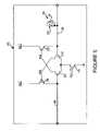
- the bidirectional buffer 200operates in either of two modes, namely a pre-charge mode in which a Pc signal is high and a PcF signal is low, and a read/write mode in which the Pc signal is low and the PcF signal is high.
- the buffer 200includes a pair of NMOS transistors 202 , 204 that have their gates coupled to respective segments 206 , 208 of a respective LDRW line.
- the sources of the transistors 202 , 204are selectively coupled to ground through another NMOS transistor 210 that is turned ON in the read/write mode by a high PcF signal applied to the gate of the transistor 210 .
- the drain of the transistor 202is connected to both the gate of a PMOS transistor 220 and the drain of a second PMOS transistor 222 .
- the drain of the transistor 204is connected to both the gate of a PMOS transistor 226 and the drain of a second PMOS transistor 228 .
- the gates of the PMOS transistors 222 , 228are coupled to each other and are driven with the PcF signal so that they are turned OFF in the read/write mode when the PcF signal is high.
- Each LDRW line segment 206 , 208is connected to the drain of a respective NMOS transistor 230 , 232 , which implement a precharge circuit 234 .
- a latch 240 formed by two back-to-back inverters 242 , 244is connected to the LDRW line segment 208 .
- FIG. 4shows the buffer 200 without the transistors that are turned OFF by the low PcF signal and the high Pc signal in the precharge mode.
- the low PcF signalturns on the PMOS transistors 222 , 228 thereby driving the gates of the PMOS transistors 220 , 226 high to turn OFF the PMOS transistors 220 , 226 .
- the transistors 220 , 226are not shown in FIG. 4 .
- the high Pc enable signalturns ON the NMOS transistors 230 , 232 in the precharge circuit 234 thereby driving the LDRW line segments 206 , 208 to ground.
- the ground applied to the LDRW line segments 206 , 208turns OFF the NMOS transistors 202 , 204 .
- the low PcF signalturns OFF the transistor 210 . It is again for that reason the transistors 202 , 204 , 210 are not shown in FIG. 4 .
- the LDRW line segments 206 , 208are driven to ground.
- the effective configuration of the bidirectional buffer 200 in the read/write modeis shown in FIG. 5 and with continued reference to FIG. 3 .
- the high PcF signalturns OFF the PMOS transistors 222 , 228
- the low Pc signalturns OFF the transistors 230 , 232 .
- these transistors 222 , 228 , 230 , 232are not shown in FIG. 5 .
- the LDRW line segments 206 , 208will have been precharged low, as explained above. Therefore, if a low data signal is applied to, for example, the line segment 206 , the transistor 202 will remain in an OFF condition.
- latch 240will keep the buffer 200 in its precharged state so that the other LDRW line segment 208 will remain low.
- the NMOS transistor 202will be turned ON, thereby pulling the gate of the PMOS transistor 220 low.
- the transistor 220will then be turned ON thereby driving the LDRW line segment 208 high.
- the high data signal applied to the segment 206is coupled to the segment 208 .
- the LDRW line segment 208is driven high, it turns ON the NMOS transistor 204 , which, in turn, turns ON the transistor 226 to maintain the line segment 206 high.
- This feedback effectalso improves the speed of the rising edge of the line segment 206 .
- the bidirectional buffer 200essentially latches the LDRW line segments 206 , 208 high.
- the latch 240is not needed to maintain the line segments 206 , 208 high in the read/write mode, although it does serve to maintain the LDRW line segments 206 , 208 low in the read/write mode after they have been precharged but before data signals have been applied to the bidirectional buffer 200 .
- the bidirectional buffer 200operates in essentially the same manner when a data signal is applied to the line segment 208 since
- bidirectional buffer shown in FIG. 3is used when the LDRW lines 206 , 208 are precharged low and driven high.
- bidirectional buffersaccording to other embodiments of the invention can be used when the LDRW lines 206 , 208 are precharged high and driven low.
- such bidirectional bufferscan be implemented by substituting transistors of a first conductivity type for transistors of a second conductivity type, and vice-versa, where the second conductivity type is different from the first conductivity type.
- NMOS transistorsare substituted for the PMOS transistors used in the bidirectional buffer 200
- PMOS transistorsare substituted for the NMOS transistors used in the bidirectional buffer 200 .
- FIG. 6illustrates a portion of a memory device 300 according to an embodiment of the invention.
- the memory device 300includes an array 302 of memory cells, which may be, for example, DRAM memory cells, SRAM memory cells, flash memory cells, or some other types of memory cells.
- the memory device 300includes a command decoder 306 that receives memory commands through a command bus 308 and generates corresponding control signals within the memory device 300 to carry out various memory operations.
- Row and column address signalsare applied to the memory device 300 through an address bus 320 and provided to an address latch 310 .
- the address latchthen outputs a separate column address and a separate row address.
- the row and column addressesare provided by the address latch 310 to a row address decoder 322 and a column address decoder 328 , respectively.
- the column address decoder 328selects digit lines extending through the array 302 corresponding to driver 324 that activates respective rows of memory cells in the array 302 corresponding to received row addresses.
- the selected data linee.g., a digit line
- the selected data linecorresponding to a received column address are coupled to a read/write circuitry 330 to provide read data to a data output buffer 334 via an input-output data bus 340 .
- Write dataare applied to the memory array 302 through a data input buffer 344 and the memory array read/write circuitry 330 .
- the command decoder 306responds to memory commands applied to the command bus 308 to perform various operations on the memory array 302 . In particular, the command decoder 306 is used to generate internal control signals to read data from and write data to the memory array 302 .
- Bidirectional buffers 346are included in the memory array 302 .
- each of the LDRW linesare divided into at least two segments, and the bidirectional buffers 346 are interposed between adjacent segments of each LDRW line.
- data lines in the array 302 other than LDRW lines, such as digit linesare divided into at least two segments, and the bidirectional buffers 346 are interposed between adjacent segments of respective data lines.
- other signal lines in the memory array 302such as, for example, word lines, are divided into at least two segments, and the bidirectional buffers 346 are interposed between adjacent segments of each word line.
Landscapes
- Engineering & Computer Science (AREA)
- Microelectronics & Electronic Packaging (AREA)
- Computer Hardware Design (AREA)
- Databases & Information Systems (AREA)
- Static Random-Access Memory (AREA)
- Dram (AREA)
Abstract
Description
- This invention relates to memory devices, and, more particularly, to a signal coupling buffer and method for coupling signals through a memory array.
- A wide variety of memory devices are in common use. Commonly used memory devices include dynamic random access memory (“DRAM”) devices, static random access memory (“SRAM”) devices, flash memory devices, and programmable read only memory (“PROM”) devices, to name a few. All of these memory devices have certain properties in common. For example, the capacity and operating speed of such memory devices have continuously increased with time. Also, these memory devices utilize a large number of memory cells that are arranged in arrays or banks containing rows and columns.
- Each bank of memory cells can be thought of as a memory device “building block” so that the capacity of a memory device can be increased simply by increasing the number of banks in the memory device. For example, as illustrated in
FIG. 1 , an architecture for amemory device 10 includes a plurality of data terminals12a-zfor coupling write data to and read data from thememory device 10. The data terminals12 typically number in powers of 2, with 8, 16 and 32 data terminals currently being common. Each data terminals12 is selectively coupled to memory cells in thememory device 10. Thememory device 10 contains 8 banks 20-34 of memory cells fabricated in an array area of a silicon substrate, with each bank being divided into two sections a,b by arespective midgap region 40. The memory cells in the low-order banks20-26 are selectively coupled through a first plurality of common local data read/write (“LDRW”)lines 50 to a first set of respective data terminals12 on the left side of thememory device 10 as shown inFIG. 1 . However, only asingle LDRW line 50 connected to a single data terminal12 on the left side is shown inFIG. 1 for purposes of clarity, it being understood that each data terminal12 is connected to arespective LDRW line 50. Similarly, the memory cells in the high-order banks28-34 are selectively coupled through a second plurality ofLDRW lines 54 to a second set of respective data terminals12 on the right-hand side of thememory device 10, although only onesuch line 54 is shown for purposes of clarity. - As shown in
FIG. 1 , the LDRWlines terminal data drivers terminal data drivers respective LDRW lines LDRW lines circuit 70 that is fabricated in themidgap region 40 of the respective bank. The ADDs70 may be conventional or subsequently developed circuitry. As is well known in the art, each of theADDs 70 couple write data from therespective LDRW line respective LDRW line - As mentioned above, the capacity of memory devices can be increased simply by including a larger number of banks of memory cells. However, as the number of banks is increased, the lengths of the
LDRW lines LDRW lines - The problem of increased LDRW line capacitance and resistance potentially limiting memory device operating speed is also encountered in coupling data signals through data lines other than LDRW lines or other signal lines in memory arrays. For examples it is common for data lines known as bit lines or digit lines to extend through a memory array for coupling individual memory cells in the respective column of the array to a respective sense amplifier. The digit lines are, in turn, selectively coupled to the I/O lines. As the size of arrays continues to increase to provide increased memory capacity, the lengths of these digit lines are also increased, thus increasing their capacitance and resistance, which also tends to slow the operating speed of memory devices. Similar problems are encountered in coupling signals through other signal lines in an array, such as word lines.
- There is therefore a need for devices and methods for more quickly coupling data signals through data lines such as LDRW lines and through other signal lines in memory arrays so that the capacity of memory devices can be increased without limiting operating speed.
FIG. 1 is a block diagram of an architecture for a conventional memory device.FIG. 2 is a block diagram of an architecture for a memory device architecture according to an embodiment of the invention.FIG. 3 is a schematic diagram of an embodiment of a bidirectional buffer that may be used in the memory device ofFIG. 2 .FIG. 4 is a schematic diagram of the bidirectional buffer ofFIG. 3 as it is effectively configured when pre-charging a respective LDRW line instead of coupling read data or write data through the LDRW line.FIG. 5 is a schematic diagram of the bidirectional buffer ofFIG. 3 as it is effectively configured when coupling read data or write data through a respective LDRW line.FIG. 6 is a block diagram of an embodiment of a memory device according to an embodiment of the invention.- An architecture for a
memory device 100 according to an embodiment of the invention is shownFIG. 2 . Thememory device 100 includes the components of thememory device 10 shown inFIG. 1 . Therefore, in the interests of clarity and brevity, these components have been provided with the same reference numerals, and an explanation of their structure and function will not be repeated. Thememory device 100 differs from thememory device 10 shown inFIG. 1 by dividing each of theLDRW lines LDRW line segments 50a,band54a,b,respectively. A respectivebidirectional buffer segments 50a,band54a,b,respectively. Thebidirectional buffers respective LDRW lines 50 in either direction. As a result, for example, write data can be coupled from thedata terminal 12mthrough thebidirectional buffer 110 to theADD 70 of bank24 or bank26. Similarly, read data can be coupled from theADD 70 of bank26 or bank24 through thebidirectional buffer 110 to thedata terminal 12m. Moreover, thebidirectional buffers 110 can couple data in either direction between theLDRW line segments LDRW line segments buffer 110 and select the direction of signal transfer. In other words, thebidirectional drivers LDRW line 50. As a result, a relatively small amount of circuitry and fewer routes are required to implement thebidirectional buffers - Although the
memory device 100 uses only onebidirectional buffer LDRW line LDRW line bidirectional buffers - One embodiment of a
bidirectional buffer 200 that may be used for thebidirectional buffers FIG. 3 . Thebidirectional buffer 200 operates in either of two modes, namely a pre-charge mode in which a Pc signal is high and a PcF signal is low, and a read/write mode in which the Pc signal is low and the PcF signal is high. Thebuffer 200 includes a pair ofNMOS transistors respective segments transistors NMOS transistor 210 that is turned ON in the read/write mode by a high PcF signal applied to the gate of thetransistor 210. The drain of thetransistor 202 is connected to both the gate of aPMOS transistor 220 and the drain of asecond PMOS transistor 222. Similarly, the drain of thetransistor 204 is connected to both the gate of aPMOS transistor 226 and the drain of asecond PMOS transistor 228. The gates of thePMOS transistors line segment respective NMOS transistor precharge circuit 234. The gates of thetransistors latch 240 formed by two back-to-back inverters LDRW line segment 208. - The operation of the
bidirectional buffer 200 will now be explained in each of its modes. In the precharge mode, thebuffer 200 effectively assumes the configuration shown inFIG. 4 .FIG. 4 shows thebuffer 200 without the transistors that are turned OFF by the low PcF signal and the high Pc signal in the precharge mode. With reference, also, toFIG. 3 , in the precharge mode the low PcF signal turns on thePMOS transistors PMOS transistors PMOS transistors transistors FIG. 4 . At the same time, the high Pc enable signal turns ON theNMOS transistors precharge circuit 234 thereby driving theLDRW line segments LDRW line segments NMOS transistors transistor 210. It is again for that reason thetransistors FIG. 4 . Thus, in the precharge mode, theLDRW line segments - The effective configuration of the
bidirectional buffer 200 in the read/write mode is shown inFIG. 5 and with continued reference toFIG. 3 . In the read/write mode, the high PcF signal turns OFF thePMOS transistors transistors transistors FIG. 5 . When entering read/write mode, theLDRW line segments line segment 206, thetransistor 202 will remain in an OFF condition. As a result,latch 240 will keep thebuffer 200 in its precharged state so that the otherLDRW line segment 208 will remain low. - If, on the other hand, a high data signal is applied to the
LDRW line segment 206, theNMOS transistor 202 will be turned ON, thereby pulling the gate of thePMOS transistor 220 low. Thetransistor 220 will then be turned ON thereby driving theLDRW line segment 208 high. Thus, the high data signal applied to thesegment 206 is coupled to thesegment 208. When theLDRW line segment 208 is driven high, it turns ON theNMOS transistor 204, which, in turn, turns ON thetransistor 226 to maintain theline segment 206 high. This feedback effect also improves the speed of the rising edge of theline segment 206. Thus, thebidirectional buffer 200 essentially latches theLDRW line segments latch 240 is not needed to maintain theline segments LDRW line segments bidirectional buffer 200. Thebidirectional buffer 200 operates in essentially the same manner when a data signal is applied to theline segment 208 since - The bidirectional buffer shown in
FIG. 3 is used when the LDRW lines206,208 are precharged low and driven high. However, it will be understood that bidirectional buffers according to other embodiments of the invention can be used when the LDRW lines206,208 are precharged high and driven low. For example, such bidirectional buffers can be implemented by substituting transistors of a first conductivity type for transistors of a second conductivity type, and vice-versa, where the second conductivity type is different from the first conductivity type. Specifically, NMOS transistors are substituted for the PMOS transistors used in thebidirectional buffer 200, and PMOS transistors are substituted for the NMOS transistors used in thebidirectional buffer 200. Instead of coupling the NMOS transistors to ground, equivalent PMOS transistors would be coupled to Vcc, and instead of coupling the PMOS transistors to Vcc, equivalent NMOS transistors would be coupled to ground. Other embodiments may be used to precharge the LDRW lines206,208 or other data or signal lines in an array to a different voltage, and the LDRW lines206,208 or other data or signal lines can be driven to different voltage levels as desired. FIG. 6 illustrates a portion of amemory device 300 according to an embodiment of the invention. Thememory device 300 includes anarray 302 of memory cells, which may be, for example, DRAM memory cells, SRAM memory cells, flash memory cells, or some other types of memory cells. Thememory device 300 includes acommand decoder 306 that receives memory commands through acommand bus 308 and generates corresponding control signals within thememory device 300 to carry out various memory operations. Row and column address signals are applied to thememory device 300 through anaddress bus 320 and provided to anaddress latch 310. The address latch then outputs a separate column address and a separate row address.- The row and column addresses are provided by the
address latch 310 to arow address decoder 322 and acolumn address decoder 328, respectively. Thecolumn address decoder 328 selects digit lines extending through thearray 302 corresponding todriver 324 that activates respective rows of memory cells in thearray 302 corresponding to received row addresses. The selected data line (e.g., a digit line) corresponding to a received column address are coupled to a read/write circuitry 330 to provide read data to adata output buffer 334 via an input-output data bus 340. Write data are applied to thememory array 302 through adata input buffer 344 and the memory array read/write circuitry 330. Thecommand decoder 306 responds to memory commands applied to thecommand bus 308 to perform various operations on thememory array 302. In particular, thecommand decoder 306 is used to generate internal control signals to read data from and write data to thememory array 302. Bidirectional buffers 346 according to embodiments of the invention are included in thememory array 302. In some embodiments, each of the LDRW lines are divided into at least two segments, and thebidirectional buffers 346 are interposed between adjacent segments of each LDRW line. In other embodiments, data lines in thearray 302 other than LDRW lines, such as digit lines, are divided into at least two segments, and thebidirectional buffers 346 are interposed between adjacent segments of respective data lines. In still other embodiments, other signal lines in thememory array 302, such as, for example, word lines, are divided into at least two segments, and thebidirectional buffers 346 are interposed between adjacent segments of each word line. Other modifications will be apparent to one skilled in the art.- From the foregoing it will be appreciated that, although specific embodiments of the invention have been described herein for purposes of illustration, various modifications may be made without deviating from the spirit and scope of the invention. Accordingly, the invention is not limited except as by the appended claims.
Claims (25)
Priority Applications (5)
| Application Number | Priority Date | Filing Date | Title |
|---|---|---|---|
| US12/353,661US7929329B2 (en) | 2009-01-14 | 2009-01-14 | Memory bank signal coupling buffer and method |
| US13/071,303US8400809B2 (en) | 2009-01-14 | 2011-03-24 | Memory bank signal coupling buffer and method |
| US13/846,452US9601168B2 (en) | 2009-01-14 | 2013-03-18 | Memory bank signal coupling buffer and method |
| US15/405,839US10121523B2 (en) | 2009-01-14 | 2017-01-13 | Memory bank signal coupling buffer and method |
| US16/051,281US10789998B2 (en) | 2009-01-14 | 2018-07-31 | Memory bank signal coupling buffer and method |
Applications Claiming Priority (1)
| Application Number | Priority Date | Filing Date | Title |
|---|---|---|---|
| US12/353,661US7929329B2 (en) | 2009-01-14 | 2009-01-14 | Memory bank signal coupling buffer and method |
Related Child Applications (1)
| Application Number | Title | Priority Date | Filing Date |
|---|---|---|---|
| US13/071,303ContinuationUS8400809B2 (en) | 2009-01-14 | 2011-03-24 | Memory bank signal coupling buffer and method |
Publications (2)
| Publication Number | Publication Date |
|---|---|
| US20100177571A1true US20100177571A1 (en) | 2010-07-15 |
| US7929329B2 US7929329B2 (en) | 2011-04-19 |
Family
ID=42318992
Family Applications (5)
| Application Number | Title | Priority Date | Filing Date |
|---|---|---|---|
| US12/353,661Active2029-07-11US7929329B2 (en) | 2009-01-14 | 2009-01-14 | Memory bank signal coupling buffer and method |
| US13/071,303ActiveUS8400809B2 (en) | 2009-01-14 | 2011-03-24 | Memory bank signal coupling buffer and method |
| US13/846,452Active2029-08-22US9601168B2 (en) | 2009-01-14 | 2013-03-18 | Memory bank signal coupling buffer and method |
| US15/405,839ActiveUS10121523B2 (en) | 2009-01-14 | 2017-01-13 | Memory bank signal coupling buffer and method |
| US16/051,281Active - ReinstatedUS10789998B2 (en) | 2009-01-14 | 2018-07-31 | Memory bank signal coupling buffer and method |
Family Applications After (4)
| Application Number | Title | Priority Date | Filing Date |
|---|---|---|---|
| US13/071,303ActiveUS8400809B2 (en) | 2009-01-14 | 2011-03-24 | Memory bank signal coupling buffer and method |
| US13/846,452Active2029-08-22US9601168B2 (en) | 2009-01-14 | 2013-03-18 | Memory bank signal coupling buffer and method |
| US15/405,839ActiveUS10121523B2 (en) | 2009-01-14 | 2017-01-13 | Memory bank signal coupling buffer and method |
| US16/051,281Active - ReinstatedUS10789998B2 (en) | 2009-01-14 | 2018-07-31 | Memory bank signal coupling buffer and method |
Country Status (1)
| Country | Link |
|---|---|
| US (5) | US7929329B2 (en) |
Cited By (18)
| Publication number | Priority date | Publication date | Assignee | Title |
|---|---|---|---|---|
| US20110169534A1 (en)* | 2009-01-14 | 2011-07-14 | Micron Technology, Inc. | Memory bank signal coupling buffer and method |
| US8982649B2 (en)* | 2011-08-12 | 2015-03-17 | Gsi Technology, Inc. | Systems and methods involving multi-bank, dual- or multi-pipe SRAMs |
| US10521229B2 (en) | 2016-12-06 | 2019-12-31 | Gsi Technology, Inc. | Computational memory cell and processing array device using memory cells |
| US10770133B1 (en) | 2016-12-06 | 2020-09-08 | Gsi Technology, Inc. | Read and write data processing circuits and methods associated with computational memory cells that provides write inhibits and read bit line pre-charge inhibits |
| US10777262B1 (en) | 2016-12-06 | 2020-09-15 | Gsi Technology, Inc. | Read data processing circuits and methods associated memory cells |
| US10847212B1 (en) | 2016-12-06 | 2020-11-24 | Gsi Technology, Inc. | Read and write data processing circuits and methods associated with computational memory cells using two read multiplexers |
| US10847213B1 (en) | 2016-12-06 | 2020-11-24 | Gsi Technology, Inc. | Write data processing circuits and methods associated with computational memory cells |
| US10854284B1 (en) | 2016-12-06 | 2020-12-01 | Gsi Technology, Inc. | Computational memory cell and processing array device with ratioless write port |
| US10860320B1 (en) | 2016-12-06 | 2020-12-08 | Gsi Technology, Inc. | Orthogonal data transposition system and method during data transfers to/from a processing array |
| US10877731B1 (en) | 2019-06-18 | 2020-12-29 | Gsi Technology, Inc. | Processing array device that performs one cycle full adder operation and bit line read/write logic features |
| US10891076B1 (en) | 2016-12-06 | 2021-01-12 | Gsi Technology, Inc. | Results processing circuits and methods associated with computational memory cells |
| US10930341B1 (en) | 2019-06-18 | 2021-02-23 | Gsi Technology, Inc. | Processing array device that performs one cycle full adder operation and bit line read/write logic features |
| US10943648B1 (en) | 2016-12-06 | 2021-03-09 | Gsi Technology, Inc. | Ultra low VDD memory cell with ratioless write port |
| US10958272B2 (en) | 2019-06-18 | 2021-03-23 | Gsi Technology, Inc. | Computational memory cell and processing array device using complementary exclusive or memory cells |
| US10984874B1 (en)* | 2019-11-13 | 2021-04-20 | Sandisk Technologies Llc | Differential dbus scheme for low-latency random read for NAND memories |
| US10998040B2 (en) | 2016-12-06 | 2021-05-04 | Gsi Technology, Inc. | Computational memory cell and processing array device using the memory cells for XOR and XNOR computations |
| US20210280242A1 (en)* | 2012-10-12 | 2021-09-09 | Micron Technology, Inc. | Memory device architecture |
| US11227653B1 (en) | 2016-12-06 | 2022-01-18 | Gsi Technology, Inc. | Storage array circuits and methods for computational memory cells |
Families Citing this family (1)
| Publication number | Priority date | Publication date | Assignee | Title |
|---|---|---|---|---|
| US9472252B2 (en) | 2013-03-15 | 2016-10-18 | Micron Technology, Inc. | Apparatuses and methods for improving retention performance of hierarchical digit lines |
Citations (2)
| Publication number | Priority date | Publication date | Assignee | Title |
|---|---|---|---|---|
| US6882555B2 (en)* | 2003-06-18 | 2005-04-19 | Lattice Semiconductor Corporation | Bi-directional buffering for memory data lines |
| US7737727B2 (en)* | 2007-12-17 | 2010-06-15 | Intersil Americas Inc. | Bi-directional buffer for open-drain or open-collector bus |
Family Cites Families (14)
| Publication number | Priority date | Publication date | Assignee | Title |
|---|---|---|---|---|
| US4154978A (en)* | 1977-12-08 | 1979-05-15 | Operating Systems, Inc. | Self-contained bidirectional amplifying repeater |
| JPS6491221A (en)* | 1987-09-30 | 1989-04-10 | Sharp Kk | Connecting circuit for precharging bus |
| JPH047618A (en)* | 1990-04-24 | 1992-01-13 | Mitsubishi Electric Corp | Signal transmission circuit |
| US5745422A (en)* | 1996-11-12 | 1998-04-28 | International Business Machines Corporation | Cross-coupled bitline segments for generalized data propagation |
| FR2774836A1 (en)* | 1998-02-10 | 1999-08-13 | Sgs Thomson Microelectronics | BI-DIRECTIONAL TRANSMISSION DEVICE |
| US6313663B1 (en)* | 1998-03-09 | 2001-11-06 | Infineon Technologies Ag | Full swing voltage input/full swing output bi-directional repeaters for high resistance or high capacitance bi-directional signal lines and methods therefor |
| JP3425890B2 (en)* | 1999-04-08 | 2003-07-14 | Necエレクトロニクス株式会社 | Buffer circuit |
| JP2003196985A (en)* | 2001-12-25 | 2003-07-11 | Nec Electronics Corp | Semiconductor memory, bit-write method or byte-write method for semiconductor memory |
| US6664807B1 (en)* | 2002-01-22 | 2003-12-16 | Xilinx, Inc. | Repeater for buffering a signal on a long data line of a programmable logic device |
| US7142442B1 (en)* | 2004-03-08 | 2006-11-28 | Xilinx, Inc. | Segmented dataline scheme in a memory with enhanced full fault coverage memory cell testability |
| KR100663368B1 (en)* | 2005-12-07 | 2007-01-02 | 삼성전자주식회사 | Semiconductor memory device and data writing and reading method thereof |
| US7342839B2 (en)* | 2006-06-23 | 2008-03-11 | International Business Machines Corporation | Memory cell access circuit |
| JP2009059735A (en)* | 2007-08-29 | 2009-03-19 | Elpida Memory Inc | Semiconductor memory device |
| US7929329B2 (en) | 2009-01-14 | 2011-04-19 | Micron Technology, Inc. | Memory bank signal coupling buffer and method |
- 2009
- 2009-01-14USUS12/353,661patent/US7929329B2/enactiveActive
- 2011
- 2011-03-24USUS13/071,303patent/US8400809B2/enactiveActive
- 2013
- 2013-03-18USUS13/846,452patent/US9601168B2/enactiveActive
- 2017
- 2017-01-13USUS15/405,839patent/US10121523B2/enactiveActive
- 2018
- 2018-07-31USUS16/051,281patent/US10789998B2/enactiveActive - Reinstated
Patent Citations (2)
| Publication number | Priority date | Publication date | Assignee | Title |
|---|---|---|---|---|
| US6882555B2 (en)* | 2003-06-18 | 2005-04-19 | Lattice Semiconductor Corporation | Bi-directional buffering for memory data lines |
| US7737727B2 (en)* | 2007-12-17 | 2010-06-15 | Intersil Americas Inc. | Bi-directional buffer for open-drain or open-collector bus |
Cited By (35)
| Publication number | Priority date | Publication date | Assignee | Title |
|---|---|---|---|---|
| US10789998B2 (en) | 2009-01-14 | 2020-09-29 | Micron Technology, Inc. | Memory bank signal coupling buffer and method |
| US8400809B2 (en) | 2009-01-14 | 2013-03-19 | Micron Technology, Inc. | Memory bank signal coupling buffer and method |
| US9601168B2 (en) | 2009-01-14 | 2017-03-21 | Micron Technology, Inc. | Memory bank signal coupling buffer and method |
| US10121523B2 (en) | 2009-01-14 | 2018-11-06 | Micron Technology, Inc. | Memory bank signal coupling buffer and method |
| US20110169534A1 (en)* | 2009-01-14 | 2011-07-14 | Micron Technology, Inc. | Memory bank signal coupling buffer and method |
| US8982649B2 (en)* | 2011-08-12 | 2015-03-17 | Gsi Technology, Inc. | Systems and methods involving multi-bank, dual- or multi-pipe SRAMs |
| US9196324B2 (en) | 2011-08-12 | 2015-11-24 | Gsi Technology, Inc. | Systems and methods involving multi-bank, dual- or multi-pipe SRAMs |
| US9679631B2 (en) | 2011-08-12 | 2017-06-13 | Gsi Technology, Inc. | Systems and methods involving multi-bank, dual- or multi-pipe SRAMs |
| US12119055B2 (en)* | 2012-10-12 | 2024-10-15 | Micron Technology, Inc. | Memory device architecture |
| US20210280242A1 (en)* | 2012-10-12 | 2021-09-09 | Micron Technology, Inc. | Memory device architecture |
| US10860318B2 (en) | 2016-12-06 | 2020-12-08 | Gsi Technology, Inc. | Computational memory cell and processing array device using memory cells |
| US11205476B1 (en) | 2016-12-06 | 2021-12-21 | Gsi Technology, Inc. | Read data processing circuits and methods associated with computational memory cells |
| US10847212B1 (en) | 2016-12-06 | 2020-11-24 | Gsi Technology, Inc. | Read and write data processing circuits and methods associated with computational memory cells using two read multiplexers |
| US10847213B1 (en) | 2016-12-06 | 2020-11-24 | Gsi Technology, Inc. | Write data processing circuits and methods associated with computational memory cells |
| US10854284B1 (en) | 2016-12-06 | 2020-12-01 | Gsi Technology, Inc. | Computational memory cell and processing array device with ratioless write port |
| US10860320B1 (en) | 2016-12-06 | 2020-12-08 | Gsi Technology, Inc. | Orthogonal data transposition system and method during data transfers to/from a processing array |
| US10770133B1 (en) | 2016-12-06 | 2020-09-08 | Gsi Technology, Inc. | Read and write data processing circuits and methods associated with computational memory cells that provides write inhibits and read bit line pre-charge inhibits |
| US10521229B2 (en) | 2016-12-06 | 2019-12-31 | Gsi Technology, Inc. | Computational memory cell and processing array device using memory cells |
| US10891076B1 (en) | 2016-12-06 | 2021-01-12 | Gsi Technology, Inc. | Results processing circuits and methods associated with computational memory cells |
| US11763881B2 (en) | 2016-12-06 | 2023-09-19 | Gsi Technology, Inc. | Computational memory cell and processing array device using the memory cells for XOR and XNOR computations |
| US10943648B1 (en) | 2016-12-06 | 2021-03-09 | Gsi Technology, Inc. | Ultra low VDD memory cell with ratioless write port |
| US11409528B2 (en) | 2016-12-06 | 2022-08-09 | Gsi Technology, Inc. | Orthogonal data transposition system and method during data transfers to/from a processing array |
| US11257540B2 (en) | 2016-12-06 | 2022-02-22 | Gsi Technology, Inc. | Write data processing methods associated with computational memory cells |
| US10998040B2 (en) | 2016-12-06 | 2021-05-04 | Gsi Technology, Inc. | Computational memory cell and processing array device using the memory cells for XOR and XNOR computations |
| US11094374B1 (en) | 2016-12-06 | 2021-08-17 | Gsi Technology, Inc. | Write data processing circuits and methods associated with computational memory cells |
| US10725777B2 (en) | 2016-12-06 | 2020-07-28 | Gsi Technology, Inc. | Computational memory cell and processing array device using memory cells |
| US11150903B2 (en) | 2016-12-06 | 2021-10-19 | Gsi Technology, Inc. | Computational memory cell and processing array device using memory cells |
| US11194519B2 (en) | 2016-12-06 | 2021-12-07 | Gsi Technology, Inc. | Results processing circuits and methods associated with computational memory cells |
| US11227653B1 (en) | 2016-12-06 | 2022-01-18 | Gsi Technology, Inc. | Storage array circuits and methods for computational memory cells |
| US10777262B1 (en) | 2016-12-06 | 2020-09-15 | Gsi Technology, Inc. | Read data processing circuits and methods associated memory cells |
| US11194548B2 (en) | 2019-06-18 | 2021-12-07 | Gsi Technology, Inc. | Processing array device that performs one cycle full adder operation and bit line read/write logic features |
| US10958272B2 (en) | 2019-06-18 | 2021-03-23 | Gsi Technology, Inc. | Computational memory cell and processing array device using complementary exclusive or memory cells |
| US10930341B1 (en) | 2019-06-18 | 2021-02-23 | Gsi Technology, Inc. | Processing array device that performs one cycle full adder operation and bit line read/write logic features |
| US10877731B1 (en) | 2019-06-18 | 2020-12-29 | Gsi Technology, Inc. | Processing array device that performs one cycle full adder operation and bit line read/write logic features |
| US10984874B1 (en)* | 2019-11-13 | 2021-04-20 | Sandisk Technologies Llc | Differential dbus scheme for low-latency random read for NAND memories |
Also Published As
| Publication number | Publication date |
|---|---|
| US9601168B2 (en) | 2017-03-21 |
| US10121523B2 (en) | 2018-11-06 |
| US7929329B2 (en) | 2011-04-19 |
| US8400809B2 (en) | 2013-03-19 |
| US20130215699A1 (en) | 2013-08-22 |
| US10789998B2 (en) | 2020-09-29 |
| US20180336939A1 (en) | 2018-11-22 |
| US20110169534A1 (en) | 2011-07-14 |
| US20170125075A1 (en) | 2017-05-04 |
Similar Documents
| Publication | Publication Date | Title |
|---|---|---|
| US10789998B2 (en) | Memory bank signal coupling buffer and method | |
| US10867681B2 (en) | SRAM memory having subarrays with common IO block | |
| US10153007B2 (en) | Apparatuses including a memory array with separate global read and write lines and/or sense amplifier region column select line and related methods | |
| US7986547B2 (en) | Semiconductor memory device | |
| JPH0373080B2 (en) | ||
| US7692974B2 (en) | Memory cell, memory device, device and method of accessing a memory cell | |
| CN108352179B (en) | SRAM Architecture for Leak Reduction | |
| TWI509608B (en) | Column select multiplexer and method for static random-access memory and computer memory subsystem employing the same | |
| US6378008B1 (en) | Output data path scheme in a memory device | |
| KR20010038792A (en) | Semiconductor memory device uniformiting sensing efficiency of data line sense amplifier | |
| US5808482A (en) | Row decoder with level translator | |
| US8107278B2 (en) | Semiconductor storage device | |
| KR20010059017A (en) | IO structure of semiconductor memory device | |
| US9479167B2 (en) | Apparatuses and methods for line charge sharing | |
| US5392242A (en) | Semiconductor memory device with single data line pair shared between memory cell arrays | |
| US7289385B2 (en) | Bank selection signal control circuit for use in semiconductor memory device, and bank selection control method | |
| TWI750977B (en) | Array edge repeater in memory device | |
| US6597201B1 (en) | Dynamic predecoder circuitry for memory circuits | |
| JP2002352581A (en) | Semiconductor integrated circuit | |
| KR20000003989A (en) | Sram device having re-write circuit | |
| US7142465B2 (en) | Semiconductor memory | |
| KR100367159B1 (en) | Semiconductor memory device | |
| US8553483B2 (en) | Semiconductor memory device | |
| JP2008103055A (en) | Memory | |
| US6847579B2 (en) | Semiconductor memory device |
Legal Events
| Date | Code | Title | Description |
|---|---|---|---|
| AS | Assignment | Owner name:MICRON TECHNOLOGY, INC., IDAHO Free format text:ASSIGNMENT OF ASSIGNORS INTEREST;ASSIGNORS:SHORI, AIDAN;CHOPRA, SUMIT;REEL/FRAME:022107/0151 Effective date:20090106 | |
| FEPP | Fee payment procedure | Free format text:PAYOR NUMBER ASSIGNED (ORIGINAL EVENT CODE: ASPN); ENTITY STATUS OF PATENT OWNER: LARGE ENTITY | |
| STCF | Information on status: patent grant | Free format text:PATENTED CASE | |
| FPAY | Fee payment | Year of fee payment:4 | |
| AS | Assignment | Owner name:U.S. BANK NATIONAL ASSOCIATION, AS COLLATERAL AGENT, CALIFORNIA Free format text:SECURITY INTEREST;ASSIGNOR:MICRON TECHNOLOGY, INC.;REEL/FRAME:038669/0001 Effective date:20160426 Owner name:U.S. BANK NATIONAL ASSOCIATION, AS COLLATERAL AGEN Free format text:SECURITY INTEREST;ASSIGNOR:MICRON TECHNOLOGY, INC.;REEL/FRAME:038669/0001 Effective date:20160426 | |
| AS | Assignment | Owner name:MORGAN STANLEY SENIOR FUNDING, INC., AS COLLATERAL AGENT, MARYLAND Free format text:PATENT SECURITY AGREEMENT;ASSIGNOR:MICRON TECHNOLOGY, INC.;REEL/FRAME:038954/0001 Effective date:20160426 Owner name:MORGAN STANLEY SENIOR FUNDING, INC., AS COLLATERAL Free format text:PATENT SECURITY AGREEMENT;ASSIGNOR:MICRON TECHNOLOGY, INC.;REEL/FRAME:038954/0001 Effective date:20160426 | |
| AS | Assignment | Owner name:U.S. BANK NATIONAL ASSOCIATION, AS COLLATERAL AGENT, CALIFORNIA Free format text:CORRECTIVE ASSIGNMENT TO CORRECT THE REPLACE ERRONEOUSLY FILED PATENT #7358718 WITH THE CORRECT PATENT #7358178 PREVIOUSLY RECORDED ON REEL 038669 FRAME 0001. ASSIGNOR(S) HEREBY CONFIRMS THE SECURITY INTEREST;ASSIGNOR:MICRON TECHNOLOGY, INC.;REEL/FRAME:043079/0001 Effective date:20160426 Owner name:U.S. BANK NATIONAL ASSOCIATION, AS COLLATERAL AGEN Free format text:CORRECTIVE ASSIGNMENT TO CORRECT THE REPLACE ERRONEOUSLY FILED PATENT #7358718 WITH THE CORRECT PATENT #7358178 PREVIOUSLY RECORDED ON REEL 038669 FRAME 0001. ASSIGNOR(S) HEREBY CONFIRMS THE SECURITY INTEREST;ASSIGNOR:MICRON TECHNOLOGY, INC.;REEL/FRAME:043079/0001 Effective date:20160426 | |
| AS | Assignment | Owner name:JPMORGAN CHASE BANK, N.A., AS COLLATERAL AGENT, ILLINOIS Free format text:SECURITY INTEREST;ASSIGNORS:MICRON TECHNOLOGY, INC.;MICRON SEMICONDUCTOR PRODUCTS, INC.;REEL/FRAME:047540/0001 Effective date:20180703 Owner name:JPMORGAN CHASE BANK, N.A., AS COLLATERAL AGENT, IL Free format text:SECURITY INTEREST;ASSIGNORS:MICRON TECHNOLOGY, INC.;MICRON SEMICONDUCTOR PRODUCTS, INC.;REEL/FRAME:047540/0001 Effective date:20180703 | |
| AS | Assignment | Owner name:MICRON TECHNOLOGY, INC., IDAHO Free format text:RELEASE BY SECURED PARTY;ASSIGNOR:U.S. BANK NATIONAL ASSOCIATION, AS COLLATERAL AGENT;REEL/FRAME:047243/0001 Effective date:20180629 | |
| MAFP | Maintenance fee payment | Free format text:PAYMENT OF MAINTENANCE FEE, 8TH YEAR, LARGE ENTITY (ORIGINAL EVENT CODE: M1552); ENTITY STATUS OF PATENT OWNER: LARGE ENTITY Year of fee payment:8 | |
| AS | Assignment | Owner name:MICRON TECHNOLOGY, INC., IDAHO Free format text:RELEASE BY SECURED PARTY;ASSIGNOR:MORGAN STANLEY SENIOR FUNDING, INC., AS COLLATERAL AGENT;REEL/FRAME:050937/0001 Effective date:20190731 | |
| AS | Assignment | Owner name:MICRON SEMICONDUCTOR PRODUCTS, INC., IDAHO Free format text:RELEASE BY SECURED PARTY;ASSIGNOR:JPMORGAN CHASE BANK, N.A., AS COLLATERAL AGENT;REEL/FRAME:051028/0001 Effective date:20190731 Owner name:MICRON TECHNOLOGY, INC., IDAHO Free format text:RELEASE BY SECURED PARTY;ASSIGNOR:JPMORGAN CHASE BANK, N.A., AS COLLATERAL AGENT;REEL/FRAME:051028/0001 Effective date:20190731 | |
| MAFP | Maintenance fee payment | Free format text:PAYMENT OF MAINTENANCE FEE, 12TH YEAR, LARGE ENTITY (ORIGINAL EVENT CODE: M1553); ENTITY STATUS OF PATENT OWNER: LARGE ENTITY Year of fee payment:12 |